WO2023013649A1 - データキャッシュ装置およびプログラム - Google Patents
データキャッシュ装置およびプログラム Download PDFInfo
- Publication number
- WO2023013649A1 WO2023013649A1 PCT/JP2022/029689 JP2022029689W WO2023013649A1 WO 2023013649 A1 WO2023013649 A1 WO 2023013649A1 JP 2022029689 W JP2022029689 W JP 2022029689W WO 2023013649 A1 WO2023013649 A1 WO 2023013649A1
- Authority
- WO
- WIPO (PCT)
- Prior art keywords
- data
- unit
- read
- cache device
- prediction table
- Prior art date
- Legal status (The legal status is an assumption and is not a legal conclusion. Google has not performed a legal analysis and makes no representation as to the accuracy of the status listed.)
- Ceased
Links
Images



Classifications
-
- G—PHYSICS
- G06—COMPUTING OR CALCULATING; COUNTING
- G06F—ELECTRIC DIGITAL DATA PROCESSING
- G06F12/00—Accessing, addressing or allocating within memory systems or architectures
- G06F12/02—Addressing or allocation; Relocation
- G06F12/08—Addressing or allocation; Relocation in hierarchically structured memory systems, e.g. virtual memory systems
- G06F12/0802—Addressing of a memory level in which the access to the desired data or data block requires associative addressing means, e.g. caches
- G06F12/0866—Addressing of a memory level in which the access to the desired data or data block requires associative addressing means, e.g. caches for peripheral storage systems, e.g. disk cache
-
- G—PHYSICS
- G06—COMPUTING OR CALCULATING; COUNTING
- G06F—ELECTRIC DIGITAL DATA PROCESSING
- G06F12/00—Accessing, addressing or allocating within memory systems or architectures
- G06F12/02—Addressing or allocation; Relocation
- G06F12/08—Addressing or allocation; Relocation in hierarchically structured memory systems, e.g. virtual memory systems
- G06F12/0802—Addressing of a memory level in which the access to the desired data or data block requires associative addressing means, e.g. caches
- G06F12/0875—Addressing of a memory level in which the access to the desired data or data block requires associative addressing means, e.g. caches with dedicated cache, e.g. instruction or stack
-
- G—PHYSICS
- G06—COMPUTING OR CALCULATING; COUNTING
- G06F—ELECTRIC DIGITAL DATA PROCESSING
- G06F12/00—Accessing, addressing or allocating within memory systems or architectures
- G06F12/02—Addressing or allocation; Relocation
- G06F12/08—Addressing or allocation; Relocation in hierarchically structured memory systems, e.g. virtual memory systems
- G06F12/12—Replacement control
- G06F12/121—Replacement control using replacement algorithms
- G06F12/126—Replacement control using replacement algorithms with special data handling, e.g. priority of data or instructions, handling errors or pinning
-
- G—PHYSICS
- G06—COMPUTING OR CALCULATING; COUNTING
- G06F—ELECTRIC DIGITAL DATA PROCESSING
- G06F13/00—Interconnection of, or transfer of information or other signals between, memories, input/output devices or central processing units
- G06F13/14—Handling requests for interconnection or transfer
-
- Y—GENERAL TAGGING OF NEW TECHNOLOGICAL DEVELOPMENTS; GENERAL TAGGING OF CROSS-SECTIONAL TECHNOLOGIES SPANNING OVER SEVERAL SECTIONS OF THE IPC; TECHNICAL SUBJECTS COVERED BY FORMER USPC CROSS-REFERENCE ART COLLECTIONS [XRACs] AND DIGESTS
- Y02—TECHNOLOGIES OR APPLICATIONS FOR MITIGATION OR ADAPTATION AGAINST CLIMATE CHANGE
- Y02D—CLIMATE CHANGE MITIGATION TECHNOLOGIES IN INFORMATION AND COMMUNICATION TECHNOLOGIES [ICT], I.E. INFORMATION AND COMMUNICATION TECHNOLOGIES AIMING AT THE REDUCTION OF THEIR OWN ENERGY USE
- Y02D10/00—Energy efficient computing, e.g. low power processors, power management or thermal management
Definitions
- the present disclosure relates to a data cache device that temporarily holds digital data.
- inference is performed by continuously executing convolutional operations. That is, the convolution operation is performed on the original input data by a predetermined algorithm, and the convolution operation is further performed on the output data by the following algorithm.
- a layer the process of performing a convolution operation on one piece of input data and obtaining an output is called a layer.
- an algorithm for convolution operation is defined for each layer, and a network is constructed by combining these layers.
- the weight value is multiplied with the input data, and the sum of products operation is performed by adding the result.
- This weight value is defined by the kernel size by the convolution algorithm.
- Patent Document 1 is known as a semiconductor device capable of reducing power consumption.
- Japanese Patent Application Laid-Open No. 2002-200000 the power supply to a set with a low access frequency among the sets in the cache memory is cut off.
- a neural network processing device may be equipped with a cache device.
- a typical cache device stores data once read from the outside in an internal cache device based on temporal proximity or positional proximity. When the same data is read again, the data is read from the cache device without accessing to the outside.
- This cache device can be expected to have the effect of hiding the time delay caused by reading data from the outside. Also, it is possible to reduce the power consumption due to the difference in implementation between the external storage device and the cache device.
- input data may be cut out in processing units, and multiple layers of processing may be continuously performed on the cut out input data.
- the output data of a layer can be immediately reused as the next input data, and unnecessary memory accesses and delays can be reduced.
- an object of the present disclosure is to provide a data cache device that is effective in reducing power consumption.
- a data cache device of the present disclosure is a data cache device that temporarily holds digital data, and includes a data holding section that holds data and a data input interface section for inputting data from the outside of the data cache device.
- a data output interface unit for outputting data to the outside of said data cache device; a path for transferring data from said data input interface unit to said data holding unit; a selector section for simultaneously selecting one or more of a path for transferring data from the data holding section to the data output interface section; a selector control section for controlling the selector section; and a readout prediction table section for holding a scheduled number of readouts at which the data is read out during processing, and controls the selector section according to the number of readouts set in the readout prediction table section.
- a program of the present disclosure includes a data holding unit that holds data, a data input interface unit that inputs data from outside the data cache device, and a data output interface that outputs data to the outside of the data cache device. a path for transferring data from the data input interface section to the data holding section; a path for transferring data from the data input interface section to the data output interface section; and a path for transferring data from the data holding section.
- a program for controlling a data cache device comprising: a selector section for simultaneously selecting one or more of the paths for transferring to the data output interface section; The program functions as readout prediction table means for holding the number of readouts and selector control means for controlling the selector unit according to the number of readouts set in the readout prediction table means.
- a program according to another aspect of the present disclosure is a program that creates a table that sets whether to read data held in a data cache device or to read data from an external storage device as data necessary for executing an operation by an arithmetic device.
- a read count means for counting the number of times each data is read during execution of a calculation by performing an arithmetic simulation of the arithmetic unit by means of an arithmetic simulator;
- This is a program for functioning as table creation means for creating a table.
- FIG. 1 is a diagram showing the configuration of a data cache device according to the first embodiment
- FIG. 2 is a diagram showing the overall configuration of an arithmetic device including a data cache device according to the first embodiment
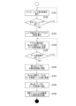
- FIG. 3 is a flowchart showing the operation of the data cache device of the first embodiment
- FIG. 4 is a diagram showing the configuration of a data cache device according to the second embodiment
- FIG. 5 is a diagram showing the configuration of a data cache device according to the third embodiment
- FIG. 6 is a flowchart showing the operation of the data cache device of the third embodiment
- FIG. 7 is a diagram showing the configuration of a data cache device according to the fourth embodiment.
- FIG. 1 shows the configuration of the data cache device 1 of the first embodiment
- FIG. 2 shows the overall configuration including the data cache device 1, the external storage device 2, the arithmetic device 3, and the arithmetic algorithm control unit 4.
- the data cache device 1 is connected to an external storage device 2 , an arithmetic device 3 and an arithmetic algorithm control section 4 .
- the data cache device 1 inputs data from the external storage device 2 , holds part of the data, and outputs the data to the arithmetic device 3 .
- the arithmetic algorithm control unit 4 manages layer parameters and algorithms of the neural network, and controls the data cache device 1 and the arithmetic device 3 in conjunction.
- 101 is a data holding unit.
- This data holding unit 101 is a cache memory that temporarily holds the Weight data of the neural network in this embodiment.
- the data holding unit 101 is implemented with an SRAM or flip-flop circuit. Note that the data holding unit 101 is also called a "local buffer”.
- Data input interface unit 102 is a data input interface unit 102 .
- Data input interface unit 102 is connected to external storage device 2 and receives data from external storage device 2 .
- a bus interface or the like may be provided in the middle, so long as the data can be logically acquired.
- the data input interface section 102 includes a function as a bus master, and acquires data from the external storage device 2 in response to a request transmitted from the arithmetic device 3 via the selector section 104 .
- the data output interface section 103 is a data output interface.
- the data output interface section 103 is connected to the arithmetic device 3 .
- the selector unit 104 is a selector unit.
- the selector unit 104 is a circuit that selects the destination of input data from the data input interface unit 102 and the source of request data from the data output interface unit 103 .
- Selector control unit 105 is a selector control unit.
- the selector control unit 105 is a part that controls the selector unit 104, and controls connection of the selector unit 104 in units of instruction execution cycles.
- Selector control section 105 includes a path for transferring data from data input interface section 102 to data holding section 101, a path for transferring data from data input interface section 102 to data output interface section 103, and a path for transferring data from data holding section 101 to data output interface section 103. , one or a plurality of paths are selected at the same time from the paths for transferring the data of .
- the read counter unit 106 is a read counter unit.
- the read counter unit 106 has a function of counting the number of times the data output interface unit 103 is accessed. It internally holds a plurality of counters, and independently counts readout for each address requested by the arithmetic unit 3 via the data output interface unit 103 .
- the reading prediction table unit 107 is a read prediction table section.
- the reading prediction table unit 107 is implemented by an SRAM or a flip-flop circuit, and stores the number of times the weight value in each layer is read. The predicted number of times may be written as an initial value when the system is started, and then updated at any timing. Also, depending on the implementation policy, only the magnitude relationship with the previously set read number threshold may be retained.
- the readout prediction table control unit 108 is a read prediction table control unit.
- the readout prediction table control unit 108 acquires the algorithm information specified by the arithmetic algorithm control unit 4, reads out the weight data readout prediction number for the corresponding layer from the readout prediction table unit 107, and sends a selector selection signal to the selector control unit 105. to be issued.
- the read prediction table control unit 108 has a function of acquiring read counter information from the read counter unit 106 and updating the values of the read prediction table unit 107 based on instructions from the arithmetic algorithm control unit 4 .
- FIG. 3 is a flowchart showing the operation of the data cache device 1.
- the computation device 3 will be described as an example of computation for moving image processing using a neural network.
- the computing device 3 performs image processing for each frame that constitutes a moving image. More specifically, a frame image or feature map to be processed is divided into a plurality of processing unit regions, and the regions are called tiles, and inference processing is performed by a neural network for each tile. The inference process performed for each frame is the same.
- the reading prediction table control unit 108 receives a list of algorithms to be processed from the arithmetic algorithm control unit 4 .
- the information includes the number of layers, the number of kernels in each layer, the number of input data channels, the number of output data channels, and the input activation size.
- the readout prediction table control unit 108 calculates the required weight retention amount and the number of tiles for which the calculation is to be repeated.
- the calculation algorithm control unit 4 itself may calculate the weight retention amount and receive the result.
- the read prediction table control unit 108 determines whether or not the required weight holding amount is equal to or less than the capacity of the data holding unit. If the amount of weight required for multi-layer processing is equal to or less than the capacity of the data holding unit 101 ("Yes" in S001), the reading prediction table control unit 108 continues the process of step S002.
- step S002 the reading prediction table control unit 108 receives information on the number of tiles when processing multiple layers from the arithmetic algorithm control unit 4, and determines whether the number of tiles is two or more.
- the read prediction table control unit 108 updates the read prediction table unit 107 so that the data is directly transferred from the external storage device 2 without going through the data holding unit 101 . If the number of tiles is 2 or more ("Yes" in S002), proceed to step S004, and update the readout prediction table unit 107 with a flag indicating that the entire region of the prediction table is to be transferred to the data holding unit 101. do. Note that the order of determination in steps S001 and S002 described above may be reversed.
- step S012 data is transferred from the external storage device 2 according to the reading prediction table section 107. Specifically, when the number of tiles to be processed is 1, the data is directly transferred without going through the data holding unit 101, and when the number of tiles to be processed is 2 or more, the data is transferred from the external storage device 2 to the data holding unit 101. .
- step S001 if the amount of Weight data is equal to or greater than the capacity of the data storage unit 101 in step S001 ("No" in S001), the process proceeds to step S005, and the data in the data storage unit 101 is stored in descending order of the number of tiles processed.
- the reading prediction table unit 107 is updated so that the weight data for the layers up to the capacity is transferred to the data holding unit 101 .
- Step S006 is a step of transferring the Weight data to be read from the data holding unit 101 from the external storage device 2 to the data holding unit 101.
- the readout prediction table control unit 108 sends a readout request to the data input interface unit 102 for weight data that needs to be read out from the data holding unit 101 .
- the request may be notified via the arithmetic algorithm control unit 4 .
- the data input interface unit 102 transfers Weight data to be newly read from the data holding unit 101 from the external storage device 2 to the data holding unit 101 .
- the data input interface unit 102 functions as a bus master, generates the address of the external storage device 2 from the weight position information held in the read prediction table, and issues a data transfer request.
- equivalent functions may be replaced.
- Step S007 and subsequent steps are steps after the start of the processing of the first tile.
- Step S007 is the timing at which the arithmetic algorithm control unit 4 sends a processing start signal to the arithmetic unit 3, and the arithmetic unit 3 sends a request to acquire the necessary weight data to the data output interface unit 103 together with the address. Occur.
- the data output interface unit 103 receives a weight data transfer request from the arithmetic unit 3 together with an address. At this time, data output interface section 103 transmits the requested address information to selector control section 105 .
- the selector control unit 105 refers to the read prediction table unit 107 to determine whether the requested data exists in the external storage device 2 or is held in the data holding unit 101, controls the selector unit 104, A path to the storage area is connected so that the data output interface unit 103 can access the data.
- the selector control unit 105 notifies the data output interface unit 103 of map information indicating whether the data exists in the external storage device 2 or in the data holding unit 101 as a path establishment signal.
- the data output interface unit 103 increments the requested transfer data amount of the read counter unit 106 for each information indicating which layer's weight data the data requested by itself belongs to and the map information returned from the selector control unit 105 . Based on the map information, the read counter unit 106 counts and holds the number of times the weight data is read from the data holding unit and the number of times the weight data is directly read from the data input interface unit.
- step S008 the arithmetic unit 3 continues to acquire Weight data via the data output interface unit 103 until all tiles are completed. During this time, data output interface section 103 continues step S007. If the processing of all tiles is completed in step S008 ("Yes" in S008), the process proceeds to step S009. In the processing up to this point, the read counter unit 106 counts the number of times the weight data is read in each layer when one frame is processed.
- step S ⁇ b>009 the readout prediction table control unit 108 reads count data from the readout counter unit 106 for each layer, and compares it with a threshold specified in advance by the arithmetic algorithm control unit 4 .
- the threshold is calculated from the amount of power consumed for reading and transferring data. That is, the amount of power required to transfer data from the external storage device 2 without going through the data holding unit 101 and the amount of power required to transfer data from the external storage device 2 to the data holding unit 101 and read data from the data holding unit 101 is determined based on the amount of power required for
- reading the weight data from the data holding unit 101 consumes less power than obtaining the data directly from the external storage device 2 .
- the reading prediction table control unit 108 compares the weight data reading count with the threshold value, and sets a flag for the weight data of the layer whose reading count is equal to or greater than the threshold value. In step S ⁇ b>010 , the flag information set in step S ⁇ b>009 is read out and written in the readout prediction table section 107 .
- a flag may be set in the read prediction table unit 107 to read from the data holding unit 101 in descending order of the read count, that is, in descending order of the read amount, without performing threshold evaluation in step S009.
- Step S011 is a step of transferring data to the data holding unit 101 based on the information in the reading prediction table unit 107.
- Readout prediction table control unit 108 sends a readout request to data input interface unit 102 for weight data that needs to be read out from data holding unit 101 anew. Alternatively, the request may be notified via the arithmetic algorithm control unit 4 .
- the data input interface unit 102 overwrites the weight data to be newly read from the data holding unit 101 in the area of the weight data newly read directly from the external storage device 2 .
- step S ⁇ b>006 may be executed again based on the newly updated contents of readout prediction table section 107 .
- step S013 the remaining frames are processed using the readout prediction table section 107 and the data holding section 101 prepared by the above process.
- the weight data is described as an example of the data held in the data holding unit 101, but the present disclosure is not applied only to the weight data, and other data such as activation data and other It goes without saying that it may also be applied to weighted data.
- the configuration of the data cache device 1 of this embodiment has been described above. is stored in the storage means, and the CPU executes the program, thereby realizing the data cache device 1 that performs the above-described control. Such programs are also included within the scope of this disclosure.
- the data cache device 1 of the present embodiment sets a flag in the weight data of the layer whose read count is equal to or greater than the threshold value and writes it to the read prediction table section 107 when performing the first frame processing. Since the weight data is transferred to the data holding unit 101 based on the reading prediction table unit 107, the weight data stored in the data holding unit 101 can be used when performing the remaining frame processing, thereby reducing power consumption. It is possible to improve the arithmetic performance while suppressing the In addition, when performing the remaining frame processing, power for evaluation may be reduced by stopping the counting and comparison processing of the present embodiment.
- FIG. 4 is a diagram showing the configuration of the data cache device 5 according to the second embodiment.
- the basic configuration of the data cache device 5 of the second embodiment is the same as that of the data cache device 1 of the first embodiment, but the data cache device 5 of the second embodiment is compressed. The difference is that weight data is handled.
- the data cache device 5 is connected to the external storage device 2, arithmetic device 3, and arithmetic algorithm control section 4 described in FIG.
- the data cache device 5 inputs data from the external storage device 2 , holds a part of the data, and outputs the data to the arithmetic device 3 .
- the arithmetic algorithm control unit 4 manages layer parameters and algorithms of the neural network, and controls the data cache device 5 and the arithmetic device 3 in conjunction.
- 501 is a data holding unit.
- This data holding unit 501 is a cache memory that temporarily holds Weight data.
- the data holding unit 501 is implemented with an SRAM or flip-flop circuit.
- Data input interface unit 502 is a data input interface unit.
- Data input interface unit 502 is connected to external storage device 2 and receives data from external storage device 2 .
- a bus interface or the like may be provided in the middle as long as the data can be logically acquired.
- the data input interface section 502 includes a function as a bus master, and acquires data from the external storage device 2 in response to a request transmitted from the arithmetic device 3 via the selector section 504 .
- the data output interface section 503 is a data output interface unit.
- the data output interface section 503 is connected to the arithmetic device 3 .
- a selector unit 504 is a selector part.
- a selector unit 504 is a circuit that selects the destination of input data from the data input interface unit 502 and the source of request data from the data output interface unit 503 .
- a selector control unit 505 is a selector control unit.
- a selector control unit 505 is a portion that controls the selector unit 504, and controls connection of the selector unit 504 in units of instruction execution cycles.
- a read counter unit 506 is a read counter unit.
- a read counter unit 506 has a function of counting the number of accesses to the data output interface unit 503 . It internally holds a plurality of counters, and independently counts readout for each address requested by the arithmetic unit 3 via the data output interface unit 503 .
- the reading prediction table section 507 is a read prediction table section.
- the reading prediction table section 507 is implemented by an SRAM or a flip-flop circuit, and stores the number of times weight data is read for each layer. The predicted number of times may be written as an initial value when the system is started, and then updated at any timing. Also, depending on the implementation policy, only the magnitude relationship with the previously set read number threshold may be retained.
- the readout prediction table control unit 508 is a read prediction table control unit.
- the readout prediction table control unit 508 acquires the algorithm information specified by the arithmetic algorithm control unit 4, reads out the weight data readout prediction number for the corresponding layer from the readout prediction table unit 507, and sends a selector selection signal to the selector control unit 505. to be issued.
- the read prediction table control unit 508 has a function of acquiring read counter information from the read counter unit 506 and updating the values of the read prediction table unit 507 based on instructions from the arithmetic algorithm control unit 4 .
- a data decompression unit 509 is a data decompression unit.
- a data decompression unit 509 decompresses the compressed weight data transferred based on the data request of the arithmetic unit 3 by a predetermined method.
- the method of compression is not limited to any particular method, and its algorithm does not affect the validity of this disclosure, but may be, for example, run-length encoding.
- the operation of the data cache device 5 of the second embodiment conforms to the flowchart of FIG. However, in creating the prediction table in steps S002, S003 to S005, it is necessary to calculate the compressed Weight data amount.
- weight data has been described as an example, but it goes without saying that the present disclosure is not applied only to weight, and may be applied to other data such as activation data and other weight data. stomach.
- the data cache device 5 of the second embodiment can improve the computational performance while suppressing power consumption.
- FIG. 5 is a diagram showing the configuration of the data cache device 6 according to the third embodiment.
- the data cache device 6 is connected to the external storage device 2 , arithmetic device 3 and arithmetic algorithm control section 4 .
- the data cache device 6 inputs data from the external storage device 2 , holds a part of the data, and outputs the data to the arithmetic device 3 .
- the arithmetic algorithm control unit 4 manages layer parameters and algorithms of the neural network and controls the arithmetic unit 3 .
- This weight placement program 7 is the Weight placement program. This weight placement program 7 is a program for determining whether to place the weight data in the external storage device 2 or in the data holding unit 601 .
- the arithmetic simulator 8 is a calculation simulator.
- the arithmetic simulator 8 is software that logically simulates the operations of the external storage device 2 , the arithmetic device 3 , the arithmetic algorithm control section 4 and the data cache device 6 .
- 601 is a data holding unit.
- This data holding unit 601 is a cache memory that temporarily holds Weight data.
- the data holding unit 601 is implemented with an SRAM or flip-flop circuit.
- the 602 is a data input interface unit.
- the data input interface unit 602 is connected to the external storage device 2 and receives data from the external storage device 2 .
- a bus interface or the like may be provided in the middle as long as the data can be logically acquired.
- the data input interface unit 602 includes a function as a bus master, and acquires data from the external storage device 2 in response to requests transmitted from the arithmetic unit 3 via the selector unit 604 .
- the 603 is a data output interface unit.
- the data output interface section 603 is connected to the arithmetic device 3 .
- the 604 is a selector unit.
- the selector unit 604 is a circuit that selects the destination of input data from the data input interface unit 602 and the source of request data from the data output interface unit 603 .
- the selector unit 604 connects data from the data holding unit 601 or to the data input interface unit 602 according to the request address issued by the data output interface unit 603 .
- a selector control unit 605 is a selector control unit.
- a selector control unit 605 is a portion that controls whether data is transferred from the data input interface unit 602 to the data holding unit 601 or data is sent according to a request from the data output interface unit 603 .
- the data arrangement table section 606 is a data arrangement table.
- the data arrangement table section 606 is implemented by an SRAM or a flip-flop circuit, and records which layer's Weight value is held in the data holding section 601 .
- Reference numeral 701 denotes weight arrangement table creation means.
- Weight arrangement table creation means 701 determines whether to arrange the weight data of each layer in the external storage device 2 or hold it in the data holding unit 601 based on the access frequency prediction.
- the 702 is read count means, which calculates the number of weight readouts for each layer. This read count calculation is performed by causing the calculation simulator 8 to execute layer processing, thereby acquiring the read count of each weight data from the calculation simulator 8 .
- the weight placement table creation means 701 and the read count means 702 are configured by program modules, and their functions are exhibited by executing the weight placement program 7 by a computer.
- FIG. 6 is a diagram showing the operation of the data cache device 6 of the third embodiment.
- S101 is a step in which the weight placement program 7 uses the calculation simulator 8 to perform calculation simulation.
- the weight allocation program 7 calculates the number of accesses to the weight data using the arithmetic simulator 8 based on information such as the algorithm, the number of kernels, the number of layers, the input data size, etc., which are input information to the arithmetic algorithm control unit 4. .
- the weight arrangement table creation means 701 executes this process for all tile layers, and lists the number of accesses for each layer in the read count means 702 . After step S102 is completed ("Yes" in step S102), the process proceeds to step S103.
- Step S103 is a step of counting the number of times of Weight access for each layer.
- the weight arrangement table creation means 701 sorts the read counts for each layer held in the read count means 702 in descending order.
- Steps S104 to S106 are steps for creating a weight arrangement table.
- the weight allocation table creation means 701 sets the address of the allocation table so as to arrange data in the data holding unit 601 in descending order of the number of weight accesses based on the capacity of the data holding unit 601 previously acquired. For example, when the address of the data holding unit 601 and the address of the external storage device 2 are designed independently, the address of the data holding unit 601 should be mapped to the weight area with the high access frequency.
- the processing in step S104 is performed in descending order of the number of accesses, and in step S105, it is determined whether the amount of data held in the data holding unit 601 is full. If the area of the data holding unit 601 is used up in step S105 ("Yes" in step S105), the process proceeds to step S106.
- Step S106 is a step of specifying an area to be allocated in the external storage device 2.
- the address of the external storage device 2 is specified for the weight data of the layer that could not be held in the data holding unit 601.
- Step S107 is a step of transferring the created weight arrangement table to the data arrangement table section 606 of the data cache device 6.
- the weight placement program 7 transfers the created weight placement table information to the data placement table section 606 for actual processing.
- the transfer means may read via the data input interface section 102, or the data arrangement table section 606 may be memory-mapped from an external area and transferred using an external master or the like (not shown).
- Step S108 is a step of transferring Weight data to be read from the data holding unit 601 to the data holding unit 601 according to the transferred data arrangement table unit 606.
- the data input interface unit 602 reads the data arrangement table, switches the selector unit 604 to the data holding unit 601 by the selector control unit 605 , and transfers the weight describing the address of the data holding unit 601 from the external storage device 2 .
- the transfer may be performed using the data input interface unit 102 or may be transferred by connecting an external master to the data holding unit 601 .
- Step S109 is a step of transferring data during arithmetic processing.
- the data requested by the arithmetic unit 3 reaches the selector unit 604 via the data output interface unit 603 and is acquired from the data holding unit 601 or the data input interface unit 602 .
- the data output interface unit 603 receives the necessary weight data from the arithmetic unit 3, refers to the data allocation table, and generates an address to the area where the weight is stored.
- step S109 is continued until the processing is completed.
- the data cache device 6 of the third embodiment includes a weight placement program 7 and a calculation simulator 8, and determines whether the weight data should be placed in the external storage device 2 or held in the data holding unit 601 based on the results of the calculation simulation.
- the data allocation table section 606 is updated based on the determination result. By arranging the weight data according to this data arrangement table section 606, it is possible to improve the calculation performance while suppressing the power consumption.
- FIG. 7 is a diagram showing the configuration of the data cache device 9 of the fourth embodiment.
- the basic configuration of the data cache device 9 of the fourth embodiment is the same as that of the data cache device 1 of the first embodiment. is provided with three arithmetic units 3.
- FIG. 7 illustrates a case where there are three output destinations, the number of computing devices 3 as output destinations is not limited to three, and may be two or four or more.
- the data cache device 9 is connected to the external storage device 2, arithmetic device 3, and arithmetic algorithm control section 4 described in FIG.
- the data cache device 9 inputs data from the external storage device 2 , holds a part of the data, and outputs the data to the arithmetic device 3 .
- the arithmetic algorithm control unit 4 manages layer parameters and algorithms of the neural network, and controls the data cache device 9 and the arithmetic device 3 in conjunction with each other.
- 901 is a data holding unit.
- This data holding unit 901 is a cache memory that temporarily holds Weight data.
- the data holding unit 901 is implemented with an SRAM or flip-flop circuit.
- the 902 is a data input interface unit.
- the data input interface section 902 is connected to the external storage device 2 and receives data from the external storage device 2 .
- a bus interface or the like may be provided in the middle, as long as the data can be logically acquired.
- the data input interface section 902 includes a function as a bus master, and acquires data from the external storage device 2 in response to a request transmitted from the arithmetic device 3 via the selector section 904 .
- the 903 is a data output interface unit.
- the data output interface section 903 is connected to three arithmetic units 3 .
- a selector unit 904 is a selector unit.
- a selector unit 904 is a circuit that selects the destination of input data from the data input interface unit 902 and the source of request data from the data output interface unit 903 .
- a selector control unit 905 is a selector control unit.
- a selector control unit 905 is a portion that controls the selector unit 904, and controls connection of the selector unit 904 in units of instruction execution cycles.
- a read counter unit 906 is a read counter unit.
- a read counter unit 906 has a function of counting the number of accesses to the data output interface unit 903 . It internally holds a plurality of counters, and independently counts readout for each address requested by each arithmetic unit 3 via the data output interface unit 903 .
- the reading prediction table section 907 is a read prediction table section.
- the reading prediction table section 907 is implemented by an SRAM or a flip-flop circuit, and stores the number of times the Weight value in each layer is read. In this embodiment, the number of times of reading is stored for each arithmetic unit 3 . The predicted number of times may be written as an initial value when the system is started, and then updated at any timing. Also, depending on the implementation policy, only the magnitude relationship with the previously set read number threshold may be retained.
- the readout prediction table control unit 908 is a read prediction table control unit.
- the readout prediction table control unit 908 acquires the algorithm information specified by the arithmetic algorithm control unit 4, reads out the weight data readout prediction number for the corresponding layer from the readout prediction table unit 907, and sends a selector selection signal to the selector control unit 905. to be issued.
- the read prediction table control unit 908 has a function of acquiring read counter information from the read counter unit 906 and updating the values of the read prediction table unit 907 based on instructions from the arithmetic algorithm control unit 4 .
- step S007 the data requested by the data output interface unit 103 is sent back from the selector control unit 105 together with information indicating from which arithmetic unit the data is requested and information indicating which layer Weight is.
- the requested transfer data amount of the read counter unit 106 is incremented for each piece of map information obtained.
- the number of times of reading data that is used when comparing the number of times of reading data with the threshold value is the number of times of reading that is linked to the arithmetic unit 3 used for processing.
- the reading prediction table section 907 stores the number of reading times of the weight data of each layer in association with each of the three arithmetic units A, B, and C.
- FIG. Assuming that arithmetic devices A and B are used and arithmetic device C is not used in the processing to be performed from now on, the total value of the number of times of reading linked to arithmetic devices A and B is compared with a threshold, and if the number of times of reading is equal to or greater than the threshold, Flag Weight data.
- weight data has been described as an example, but it goes without saying that the present disclosure is not applied only to weight, and may be applied to other data such as activation data and other weight data. stomach.
- the data cache device 9 of the fourth embodiment can improve the computational performance while suppressing power consumption.
- the data cache device 9 of the fourth embodiment counts the number of times of reading for each arithmetic unit 3 and stores the number of times of reading in the read prediction table unit 907, the arithmetic unit executing the processing to be performed from now on is stored. 3, Weight data to be stored in the data holding unit 901 can be determined.
- the present disclosure is not limited to the above-described embodiment.
- a flag is set for data whose number of data reads is equal to or greater than the threshold (S009), and the read prediction table is updated ( S010) and transferring data to the data holding unit based on the updated readout prediction table (S011) have been described.
- data that is effective in reducing power consumption when held in the data holding unit 101 is determined in units of frames, but this unit does not necessarily have to be in units of frames. It's okay. That is, when the processing of one tile is completed, a flag may be set for the data of the layer whose read count is equal to or greater than the threshold. In particular, this configuration is effective when the tile size is a neural network regardless of the layer.
Landscapes
- Engineering & Computer Science (AREA)
- Theoretical Computer Science (AREA)
- Physics & Mathematics (AREA)
- General Engineering & Computer Science (AREA)
- General Physics & Mathematics (AREA)
- Memory System Of A Hierarchy Structure (AREA)
Priority Applications (1)
| Application Number | Priority Date | Filing Date | Title |
|---|---|---|---|
| JP2023540369A JP7798105B2 (ja) | 2021-08-06 | 2022-08-02 | データキャッシュ装置およびプログラム |
Applications Claiming Priority (2)
| Application Number | Priority Date | Filing Date | Title |
|---|---|---|---|
| JP2021129531 | 2021-08-06 | ||
| JP2021-129531 | 2021-08-06 |
Publications (1)
| Publication Number | Publication Date |
|---|---|
| WO2023013649A1 true WO2023013649A1 (ja) | 2023-02-09 |
Family
ID=85155661
Family Applications (1)
| Application Number | Title | Priority Date | Filing Date |
|---|---|---|---|
| PCT/JP2022/029689 Ceased WO2023013649A1 (ja) | 2021-08-06 | 2022-08-02 | データキャッシュ装置およびプログラム |
Country Status (2)
| Country | Link |
|---|---|
| JP (1) | JP7798105B2 (https=) |
| WO (1) | WO2023013649A1 (https=) |
Cited By (1)
| Publication number | Priority date | Publication date | Assignee | Title |
|---|---|---|---|---|
| US20250278363A1 (en) * | 2024-03-04 | 2025-09-04 | Kioxia Corporation | Cache server and content delivery system |
Citations (6)
| Publication number | Priority date | Publication date | Assignee | Title |
|---|---|---|---|---|
| JPH0844625A (ja) * | 1994-07-28 | 1996-02-16 | Nec Software Ltd | バッファキャッシュ機構 |
| JP2004192403A (ja) * | 2002-12-12 | 2004-07-08 | Fuji Xerox Co Ltd | キャッシュメモリのデータ管理方法、及び情報処理装置 |
| JP2015525940A (ja) * | 2012-09-28 | 2015-09-07 | インテル コーポレイション | 不揮発性メモリにコードをキャッシュする方法、システムおよび装置 |
| JP2019114013A (ja) * | 2017-12-22 | 2019-07-11 | 株式会社富士通アドバンストエンジニアリング | 演算処理装置及び演算処理装置の制御方法 |
| JP2020140507A (ja) * | 2019-02-28 | 2020-09-03 | Necプラットフォームズ株式会社 | 畳み込み演算処理装置および畳み込み演算処理方法 |
| US20200327061A1 (en) * | 2017-12-29 | 2020-10-15 | Huawei Technologies Co., Ltd. | Data prefetching method and apparatus, and storage device |
-
2022
- 2022-08-02 WO PCT/JP2022/029689 patent/WO2023013649A1/ja not_active Ceased
- 2022-08-02 JP JP2023540369A patent/JP7798105B2/ja active Active
Patent Citations (6)
| Publication number | Priority date | Publication date | Assignee | Title |
|---|---|---|---|---|
| JPH0844625A (ja) * | 1994-07-28 | 1996-02-16 | Nec Software Ltd | バッファキャッシュ機構 |
| JP2004192403A (ja) * | 2002-12-12 | 2004-07-08 | Fuji Xerox Co Ltd | キャッシュメモリのデータ管理方法、及び情報処理装置 |
| JP2015525940A (ja) * | 2012-09-28 | 2015-09-07 | インテル コーポレイション | 不揮発性メモリにコードをキャッシュする方法、システムおよび装置 |
| JP2019114013A (ja) * | 2017-12-22 | 2019-07-11 | 株式会社富士通アドバンストエンジニアリング | 演算処理装置及び演算処理装置の制御方法 |
| US20200327061A1 (en) * | 2017-12-29 | 2020-10-15 | Huawei Technologies Co., Ltd. | Data prefetching method and apparatus, and storage device |
| JP2020140507A (ja) * | 2019-02-28 | 2020-09-03 | Necプラットフォームズ株式会社 | 畳み込み演算処理装置および畳み込み演算処理方法 |
Cited By (2)
| Publication number | Priority date | Publication date | Assignee | Title |
|---|---|---|---|---|
| US20250278363A1 (en) * | 2024-03-04 | 2025-09-04 | Kioxia Corporation | Cache server and content delivery system |
| US12530294B2 (en) * | 2024-03-04 | 2026-01-20 | Kioxia Corporation | Cache server and content delivery system |
Also Published As
| Publication number | Publication date |
|---|---|
| JP7798105B2 (ja) | 2026-01-14 |
| JPWO2023013649A1 (https=) | 2023-02-09 |
Similar Documents
| Publication | Publication Date | Title |
|---|---|---|
| KR102407106B1 (ko) | 프로그래밍 가능한 원자적 동작을 하는 메모리 컨트롤러 | |
| US11886365B2 (en) | DMA control circuit with quality of service indications | |
| JP5776688B2 (ja) | 情報処理装置及びタスク切り替え方法 | |
| JP5498505B2 (ja) | データバースト間の競合の解決 | |
| CN101149717A (zh) | 计算机系统及直接内存访问传输方法 | |
| JP5131188B2 (ja) | データ処理装置 | |
| JP5040050B2 (ja) | 複数チャネルdmaコントローラおよびプロセッサシステム | |
| WO2023013649A1 (ja) | データキャッシュ装置およびプログラム | |
| WO2023115529A1 (zh) | 芯片内的数据处理方法及芯片 | |
| JP2008152470A (ja) | データ処理システム及び半導体集積回路 | |
| CN116451754A (zh) | 一种支持多层神经网络层间并行处理的加速器 | |
| JP2009294990A (ja) | 画像処理システム | |
| US12190164B2 (en) | Kickslot manager circuitry for graphics processors | |
| JP2006338538A (ja) | ストリームプロセッサ | |
| KR102755426B1 (ko) | 메모리 컨트롤러 | |
| EP4384975B1 (en) | Logical slot to hardware slot mapping for graphics processors | |
| US20240095184A1 (en) | Address Translation Service Management | |
| US12175300B2 (en) | Software control techniques for graphics hardware that supports logical slots and reservation of graphics hardware based on a priority threshold | |
| WO2023038759A1 (en) | Quality of service techniques in distributed graphics processor | |
| KR102783145B1 (ko) | Dma를 이용한 데이터 처리 방법 및 전자 장치 | |
| KR102536943B1 (ko) | 데이터 절감 장치, 데이터 절감 방법 및 데이터 절감 장치를 포함하는 시스템 | |
| JP4170330B2 (ja) | 情報処理装置 | |
| US12265844B2 (en) | Quality of service techniques in distributed graphics processor | |
| JP6747680B1 (ja) | データ転送装置、データ転送方法及びコンピュータプログラム | |
| JP2006215621A (ja) | Dma制御装置 |
Legal Events
| Date | Code | Title | Description |
|---|---|---|---|
| 121 | Ep: the epo has been informed by wipo that ep was designated in this application |
Ref document number: 22853068 Country of ref document: EP Kind code of ref document: A1 |
|
| WWE | Wipo information: entry into national phase |
Ref document number: 2023540369 Country of ref document: JP |
|
| NENP | Non-entry into the national phase |
Ref country code: DE |
|
| 122 | Ep: pct application non-entry in european phase |
Ref document number: 22853068 Country of ref document: EP Kind code of ref document: A1 |