WO2023008228A1 - アンテナ、アンテナモジュール及び電子機器 - Google Patents
アンテナ、アンテナモジュール及び電子機器 Download PDFInfo
- Publication number
- WO2023008228A1 WO2023008228A1 PCT/JP2022/027832 JP2022027832W WO2023008228A1 WO 2023008228 A1 WO2023008228 A1 WO 2023008228A1 JP 2022027832 W JP2022027832 W JP 2022027832W WO 2023008228 A1 WO2023008228 A1 WO 2023008228A1
- Authority
- WO
- WIPO (PCT)
- Prior art keywords
- feeding
- antenna
- conductor
- feeding element
- feed
- Prior art date
- Legal status (The legal status is an assumption and is not a legal conclusion. Google has not performed a legal analysis and makes no representation as to the accuracy of the status listed.)
- Ceased
Links
Images


Classifications
-
- H—ELECTRICITY
- H01—ELECTRIC ELEMENTS
- H01Q—ANTENNAS, i.e. RADIO AERIALS
- H01Q13/00—Waveguide horns or mouths; Slot antennas; Leaky-waveguide antennas; Equivalent structures causing radiation along the transmission path of a guided wave
- H01Q13/08—Radiating ends of two-conductor microwave transmission lines, e.g. of coaxial lines, of microstrip lines
-
- H—ELECTRICITY
- H01—ELECTRIC ELEMENTS
- H01Q—ANTENNAS, i.e. RADIO AERIALS
- H01Q1/00—Details of, or arrangements associated with, antennas
- H01Q1/12—Supports; Mounting means
- H01Q1/22—Supports; Mounting means by structural association with other equipment or articles
- H01Q1/2283—Supports; Mounting means by structural association with other equipment or articles mounted in or on the surface of a semiconductor substrate as a chip-type antenna or integrated with other components into an IC package
-
- H—ELECTRICITY
- H01—ELECTRIC ELEMENTS
- H01Q—ANTENNAS, i.e. RADIO AERIALS
- H01Q1/00—Details of, or arrangements associated with, antennas
- H01Q1/12—Supports; Mounting means
- H01Q1/22—Supports; Mounting means by structural association with other equipment or articles
- H01Q1/24—Supports; Mounting means by structural association with other equipment or articles with receiving set
-
- H—ELECTRICITY
- H01—ELECTRIC ELEMENTS
- H01Q—ANTENNAS, i.e. RADIO AERIALS
- H01Q19/00—Combinations of primary active antenna elements and units with secondary devices, e.g. with quasi-optical devices, for giving the antenna a desired directional characteristic
- H01Q19/005—Patch antenna using one or more coplanar parasitic elements
-
- H—ELECTRICITY
- H01—ELECTRIC ELEMENTS
- H01Q—ANTENNAS, i.e. RADIO AERIALS
- H01Q21/00—Antenna arrays or systems
- H01Q21/06—Arrays of individually energised antenna units similarly polarised and spaced apart
- H01Q21/061—Two dimensional planar arrays
- H01Q21/065—Patch antenna array
-
- H—ELECTRICITY
- H01—ELECTRIC ELEMENTS
- H01Q—ANTENNAS, i.e. RADIO AERIALS
- H01Q23/00—Antennas with active circuits or circuit elements integrated within them or attached to them
-
- H—ELECTRICITY
- H01—ELECTRIC ELEMENTS
- H01Q—ANTENNAS, i.e. RADIO AERIALS
- H01Q9/00—Electrically-short antennas having dimensions not more than twice the operating wavelength and consisting of conductive active radiating elements
- H01Q9/04—Resonant antennas
- H01Q9/0407—Substantially flat resonant element parallel to ground plane, e.g. patch antenna
- H01Q9/0414—Substantially flat resonant element parallel to ground plane, e.g. patch antenna in a stacked or folded configuration
Definitions
- the present disclosure relates to an antenna, an antenna module including the antenna, and an electronic device including the antenna module.
- a patch antenna having a parasitic element is known (for example, Patent Document 1 below).
- the patch antenna described in Patent Document 1 has a reference potential layer, a feeding element, and a parasitic element.
- the feeding element is composed of a layered conductor (patch) facing the reference potential layer.
- the feed element is connected to the high frequency circuit at its feed point. That is, the feed element is fed.
- the parasitic element is composed of a layered conductor (patch) facing the feeding element from the side opposite to the reference potential layer. The parasitic element is not supplied with power and contributes to widening the band by causing multiple resonance with the feed element.
- Patent Document 1 proposes grounding the parasitic element in view of the fact that the parasitic element is charged due to the effects of radiation in outer space and then discharged, causing noise in communication. Specifically, the central portion of the parasitic element and the reference potential layer are connected by a metal rod. At this time, the central portion of the feeding element is also connected to the metal rod. Patent Document 1 states that since the electric field at the center of the antenna is zero, even if a metal rod is connected, the electromagnetic field will not be disturbed, and the radiation pattern and input impedance will not change.
- An antenna has a reference potential layer, a feeding element, a parasitic element, and at least one connecting conductor.
- the reference potential layer extends along a first direction and a second direction perpendicular to the first direction.
- the feeding element is composed of a layered conductor facing the reference potential layer. Further, the feeding element has a first feeding point on one side in the first direction of the center of the feeding element in the first direction.
- the parasitic element is composed of a layered conductor facing the feeding element from the side opposite to the reference potential layer.
- the at least one connection conductor is connected to the feed element and the parasitic element at a position closer to the center of the feed element than the first feed point in the first direction, and is connected to the reference potential layer. not electrically connected to
- An antenna includes a feed element, a parasitic element, and at least one connection conductor.
- the feeding element is composed of a layered conductor along a first direction and a second direction orthogonal to the first direction. Further, the feeding element has a first feeding point positioned on one side in the first direction from the center of the feeding element in the first direction.
- the parasitic element is composed of a layered conductor facing the feeding element.
- the at least one connection conductor is connected to the feed element and the parasitic element at a position closer to the center of the feed element than the first feed point in the first direction. Also, the at least one connection conductor includes a plurality of connection conductors whose positions in the second direction are different from each other.
- An antenna includes a feed element, a parasitic element, and at least one connection conductor.
- the feeding element is composed of a layered conductor along a first direction and a second direction orthogonal to the first direction. Further, the feeding element has a first feeding point positioned on one side in the first direction from the center of the feeding element in the first direction.
- the parasitic element is composed of a layered conductor facing the feeding element.
- the at least one connection conductor is connected to the feed element and the parasitic element at a position closer to the center of the feed element than the first feed point in the first direction. Further, the at least one connection conductor includes a connection conductor whose length in the first direction is 1/10 or more of the length of the feeding element in the first direction.
- An antenna module includes the antenna and an IC (Integrated Circuit) electrically connected to the first feeding point.
- An electronic device includes the antenna module and a housing that accommodates the antenna module.
- FIG. 1 is a perspective view of an antenna according to a first embodiment
- FIG. Sectional drawing in the II-II line of FIG. 2 is a plan perspective view of a portion of the antenna of FIG. 1
- FIG. FIG. 10 is a perspective plan view showing a modification of the connection conductor
- FIG. 11 is a perspective plan view showing another modification of the connection conductor
- FIG. 11 is a perspective plan view showing still another modification of the connection conductor
- FIG. 11 is a perspective plan view showing still another modification of the connection conductor
- FIG. 4 is a diagram showing characteristics of antennas according to an example and a comparative example
- FIG. 5 is another diagram showing the characteristics of the antennas according to the example and the comparative example; The figure which extracts and shows a part of FIG. FIG.
- FIG. 4 is a plan view schematically showing an electric field distribution in an antenna according to a comparative example;
- FIG. 4 is a plan view schematically showing electric field distribution in the antenna according to the example.
- FIG. 11 is a plan perspective view of a portion of the antenna of FIG. 10;
- the figure which shows the characteristic of the antenna which concerns on 2nd Embodiment. 8 is another diagram showing the characteristics of the antenna according to the second embodiment;
- FIG. 1 is a diagram schematically showing the configuration of an electronic device according to an embodiment;
- a rectangular coordinate system xyz fixed to the antenna may be attached to the drawing and referred to.
- An antenna may be oriented upward or downward in any direction, but for the sake of convenience, terms such as upper surface and lower surface may be used with the positive side in the z direction being oriented upward.
- Planar view means viewing in the z-direction unless otherwise specified.
- the wavelength in the description of the embodiments is the wavelength of the radio wave having the frequency targeted by the antenna (for example, the center frequency of a predetermined band).
- FIG. 1 is a perspective view showing the configuration of an antenna 1 according to the first embodiment.
- FIG. 2 is a cross-sectional view taken along line II--II of FIG.
- FIG. 3 is a plan perspective view of a part of the antenna 1 (more specifically, a range overlapping with the parasitic element 7 described later).
- the upper part of the antenna 1 is indicated by a dotted line and is seen through.
- the upper portion of the feeding conductor 9 (described later) is hidden by the feeding element 5 (described later) and is not visible, but is indicated by a solid line for convenience of illustration.
- members that are hidden behind members above and cannot be seen are also indicated by solid lines.
- the antenna 1 has laminated layered conductors (reference potential layer 3, feed element 5 and parasitic element 7).
- the feeding element 5 is connected (in other words, fed) to a high-frequency circuit via a feeding conductor 9 connected to a feeding point 17 of the feeding element 5 to transmit and/or receive radio waves.
- the parasitic element 7 is not fed with power and, for example, causes multiple resonance with the feed element 5, thereby contributing to widening the band.
- the antenna 1 has at least one (three in the illustrated example) connection conductors 11 that connect the feed element 5 and the parasitic element 7 .
- the connection conductor 11 further widens the band of the antenna 1 .
- the connection conductor 11 has various points of difference from a conductor (for example, the metal rod of JP-A-2003-100000) which is intended only for discharging the parasitic element 7 .
- connection conductor 11 is not connected to reference potential layer 3 .
- the configuration other than the connection conductor 11 may be in various forms, for example, it may be in a known form. A description of a configuration that may be a known aspect may be omitted as appropriate.
- the antenna 1 has, for example, a dielectric 13 on which the layered conductors (3, 5 and 7) described above are provided.
- the dielectric 13 contributes, for example, to supporting the layered conductor and to shortening the effective wavelength to reduce the size of the antenna 1 .
- Antenna 1 is configured to be capable of transmitting and/or receiving linearly polarized waves.
- the direction of oscillation of the linearly polarized electric field to be transmitted and/or received is the x-direction.
- the direction in which the antenna 1 has the highest gain is the +z direction. Any frequency band can be used for the antenna 1 .
- the antenna 1 may be used for transmission and/or reception of other polarized waves (for example, circularly polarized waves).
- the shape of the antenna 1 is generally a flat plate with a constant thickness. Further, the configuration of the antenna 1 is, for example, a line-symmetrical configuration with respect to a symmetrical axis (not shown) parallel to the x-direction when viewed from above. Although not particularly shown, the upper and/or lower surfaces of the antenna 1 may be overlaid with another member (for example, a dielectric layer). From another point of view, the illustrated flat plate shape may be part of a member including the antenna 1 (for example, a substrate whose thickness direction is the z direction).
- the planar shape of the antenna 1 (dielectric 13 from another point of view) shown in FIG. Not too much.
- the illustrated side of the antenna 1 is a cross section of the substrate and does not necessarily indicate the extent of the antenna 1 .
- the sides shown in FIGS. 1 and 2 may be sides of the actual antenna 1 .
- the illustrated side of the antenna 1 may be taken to indicate the range of the antenna 1 .
- the planar shape may be any shape.
- the planar shape of the antenna 1 may be a rectangular shape (illustrated example), another polygonal shape, a circular shape, or an elliptical shape.
- the size of the antenna 1 may be appropriately set according to the frequency band in which the antenna 1 is used.
- the following description may take as an example the aspect in which the antenna 1 is relatively small for use in relatively high frequency bands.
- the antenna 1 may be used in frequency bands above 300 MHz or 3 GHz, and may be used in frequency bands below 30 GHz or below 300 GHz.
- the above lower limit and upper limit may be combined appropriately.
- the lengths of the illustrated range (or the feeding element 5) in the x direction and the y direction may be 1 mm or more and 100 mm or less.
- the thickness of the antenna 1 may be, for example, 0.1 mm or more and 10 mm or less.
- Such a relatively small antenna 1 may be configured, for example, as an electronic component incorporated in an electronic device. However, the antenna 1 may have a size of several tens of centimeters or more or several meters or more in plan view.
- Each layered conductor (Matters common to various conductors)
- Each layered conductor (the reference potential layer 3, the feeding element 5 and the parasitic element 7), for example, basically spreads out without any gaps and forms a so-called solid pattern.
- Each layered conductor has a substantially constant thickness over its entire surface.
- the thickness of each layered conductor may be appropriately set in consideration of the characteristics of the antenna 1 and the like.
- the thickness may be less than the thickness of the dielectric layer.
- An example thickness of the layered conductor is 1 ⁇ m or more and 1 mm or less.
- the material of various conductor members is metal, for example.
- the metal may be any suitable such as Cu or Al.
- the materials of the various conductor members may be the same or different.
- each conductor member may be made of a single material, or may be made of a plurality of materials. The latter includes, for example, a layered conductor formed by stacking layers of different materials.
- the shaft-shaped conductor may penetrate the conductor layer, or such a distinction may not be possible.
- an aspect in which the shaft-like conductor is joined to the upper surface or the lower surface of the layered conductor may be taken as an example.
- the description of the planar shape and planar view dimensions of the antenna 1 may be used.
- the thickness of the dielectric 13 may be appropriately set so as to improve the characteristics of the antenna.
- the setting method may be, for example, the same as the setting method for a known patch antenna.
- the reference potential layer 3 overlaps the bottom surface of the dielectric 13 .
- the feeding element 5 is embedded in the dielectric 13 in a direction parallel to the upper and lower surfaces of the dielectric 13 .
- the parasitic element 7 overlaps the top surface of the dielectric 13 . Note that, unlike the illustrated example, the reference potential layer 3 and the feeding element 5 may be embedded in the dielectric 13 so as to be parallel to the upper and lower surfaces of the dielectric 13 .
- the dielectric 13 has a first dielectric layer 15A positioned between the reference potential layer 3 and the feeding element 5, and a second dielectric layer 15B positioned between the feeding element 5 and the parasitic element 7. It can be understood that The first dielectric layer 15A and the second dielectric layer 15B may be in a form in which the boundary can be specified from the viewpoint of material or the like, or they are integral with each other, and are conceptually separated simply by the presence of the feeding element 5. It may be a mode that is distinguished from.
- the dielectric 13 may be composed of a single material, or may be composed of a plurality of materials. When composed of a plurality of materials, for example, the dielectric 13 (or dielectric layer) may be configured by stacking dielectric layers made of different materials in the thickness direction, and/or glass cloth or the like.
- the base material may be impregnated with a dielectric material.
- the material of the dielectric 13 is ceramic and/or resin, for example.
- An example of the dielectric constant of the dielectric 13 is 2.0 or more and 4.0 or less.
- the reference potential layer 3 spreads without gaps and forms a so-called solid pattern. However, the reference potential layer 3 has an opening 3a at the position of the power supply conductor 9 so as not to short-circuit with the power supply conductor 9.
- FIG. The shape, diameter, etc. of the opening 3a may be appropriately set. It should be noted that the following description may be expressed ignoring the existence of the opening 3a.
- the reference potential layer 3 is arranged along a first direction and a second direction perpendicular to the first direction.
- the first direction and the second direction correspond to the x direction and the y direction in the above-described orthogonal coordinate system xyz.
- the first direction is, for example, the x direction in FIG.
- the second direction is, for example, the y direction in FIG.
- the reference potential layer 3 has, for example, a size that at least overlaps with the whole of the feed element 5 and/or the parasitic element 7 when seen through the plane.
- the outer edge of the reference potential layer 3 is, for example, entirely located outside the outer edges of the feed element 5 and/or the parasitic element 7 .
- the reference potential layer 3 may extend over the entire dielectric 13 , or part or all of the outer edge may be located inside the outer edge of the dielectric 13 .
- the reference potential layer 3 may be electrically connected to the signal ground and/or the frame ground via conductors of the circuit board on which the antenna 1 is mounted and/or conductors of the circuit board including the antenna 1 .
- the planar shape of the feeding element 5 may be, for example, various shapes that enable transmission and/or reception of linearly polarized waves in the x direction. Such shapes may include, for example, a rectangular shape (example shown) and a circular shape. The rectangular shape has two sides parallel to the x-direction and two sides parallel to the y-direction. The rectangular shape may be a square (the example shown) or a rectangle (other than a square). For the purpose of improving the characteristics, the feeding element 5 may have a modified outer edge shape based on the above-exemplified shape, or may be provided with a slit.
- the feeding element 5 may be configured as a half-wave patch, for example.
- the lengths in the x and y directions are based on 1/2 ⁇ g.
- ⁇ g is an effective wavelength at the position of the feeding element 5 considering the dielectric constant of the dielectric 13 and the like. Based on 1/2 ⁇ g, in simple theory, 1/2 ⁇ g may be used, but in practice, a length adjusted from 1/2 ⁇ g is used. because you can.
- planar shape of the feeding element 5 may basically be incorporated into the planar shape of the parasitic element 7 .
- the planar shape of the parasitic element 7 may be the same as the planar shape of the feeding element 5 (example shown in the drawing), or may be different.
- one of the feeding element 5 and the parasitic element 7 is circular and the other is rectangular, and both the feeding element 5 and the parasitic element 7 are rectangular (or circular). , in which both dimensions are different.
- the parasitic element 7 is arranged, for example, so that the center of the parasitic element 7 in the x direction coincides with the center of the feeder element 5 in the x direction when viewed through the plane.
- the feed element 5 and the parasitic element 7 have the same shape. Therefore, from another point of view, the edge portions 5a on both sides in the x direction of the feeding element 5 and the edge portions 7a on both sides in the x direction of the parasitic element 7 coincide with each other when viewed through the plane.
- the parasitic element 7 is arranged, for example, so that the y-direction center of the parasitic element 7 coincides with the y-direction center of the feed element 5 when seen from above.
- the feed element 5 and the parasitic element 7 have the same shape. Therefore, from another point of view, the edge portions 5b on both sides in the y direction of the feeding element 5 and the edge portions 7b on both sides in the y direction of the parasitic element 7 coincide with each other when viewed through the plane.
- the entire outer edge of the feeding element 5 and the entire outer edge of the parasitic element 7 match when viewed from above. Therefore, in FIG. 3 , the reference numerals for the feed element 5 are also attached in parentheses after the reference numerals for the parasitic element 7 .
- the centers and/or edges may be offset from each other for fine tuning of the properties.
- the center in the x direction or y direction may be specified rationally. For example, if a portion of the edge has a specific portion, the specific portion may be ignored. Further, for example, the position of the straight line that bisects the area of the element in the x direction may be specified as the center in the x direction.
- the feeding conductor 9 is composed of, for example, an axial conductor (via conductor) penetrating the first dielectric layer 15A. Its specific shape and dimensions may be set as appropriate. In the illustrated example, the power supply conductor 9 has a columnar shape and a straight columnar shape with the z direction as the axial direction. The upper end of the feeding conductor 9 is connected to the feeding element 5 . The lower end portion of the power supply conductor 9 is exposed to the outside through the opening 3a of the reference potential layer 3, and is connectable to an external device (for example, a high frequency circuit).
- an external device for example, a high frequency circuit
- a connection portion of the feeding element 5 with the feeding conductor 9 is a feeding point 17 .
- the term "point" is used according to convention, the feed point does not have to be point-like.
- the position of the center (for example, the geometric center) of the feeding point 17 may be referred to.
- the feed element 5 does not need to have a configuration different from that of the other regions in the feed element 5 at the position of the feed point 17, and the feed point 17 is not required to have a different structure from other regions in the feed element 5. 17 may be specified.
- the position of the feeding point 17 in the feeding element 5 in plan view is arbitrary.
- the position of the feed point 17 in the x direction may be set such that the impedance at the feed point 17 is a predetermined value (eg, 50 ⁇ ). Normally, such a position is shifted to one side in the x direction with respect to the center of the feeding element 5 in the x direction.
- the impedance adjustment may be realized by an external device connected to the power supply conductor 9 .
- the position of the feeding point 17 in the y direction may be, for example, the center of the feeding element 5 in the y direction.
- the feeding conductor may be configured by a strip (elongated layered conductor) extending parallel to the xy plane from one edge of the feeding element 5 in the x direction.
- the strip may be connected to, for example, the edge 5a (one side of the rectangle) of the feed element 5, or may be connected to the feed element 5 via a notch provided in the edge 5a.
- the notch is provided, for example, to adjust the impedance by adjusting the distance between the feeding point (connection position between the strip and the feeding element 5) and the edge 5a.
- the aspect in which the feeding element 5 has a rectangular or circular shape and/or the aspect in which the edge 5a of the feeding element 5 and the edge 7a of the parasitic element 7 are aligned are for the above-described power feeding. shall include a mode in which the notch is configured.
- connection conductor 11 is composed of, for example, an axial conductor (via conductor) penetrating the second dielectric layer 15B. Its specific shape and dimensions may be set as appropriate. In the illustrated example, the connection conductor 11 has a columnar shape and a straight columnar shape with the z direction as the axial direction. Further, for example, the diameter of the connection conductor 11 may be smaller than, equal to (the example shown in the figure), or larger than the diameter of the power supply conductor 9 .
- shapes other than the illustrated example of the connection conductor 11 include, for example, various shapes known as via conductors.
- the via conductor may be configured by connecting a plurality of small via conductors. In this case, steps and/or flanges may be formed between the small via conductors.
- the via conductor (including the above small via conductor; hereinafter the same) may have a tapered shape (frustum shape) in which the diameter decreases toward the top or bottom.
- the via conductor may be hollow. In this case, the inside of the via conductor may be in a vacuum state, filled with gas, or filled with an insulating material.
- connection region RC A region in which all (three in the illustrated example) connection conductors 11 are arranged in a plan perspective is referred to as a connection region RC (FIG. 3).
- the connection region RC may be regarded as a region of the feed element 5 or the parasitic element 7 to which the connection conductor 11 is connected.
- the connection region RC may be, for example, a minimum rectangular region that includes all of the connection conductors 11 (or their upper end surfaces or lower end surfaces) when viewed from above.
- connection region RC is positioned closer to the center of the feeding element 5 than the feeding point 17 in the x direction.
- the distance (length Lx parallel to the x direction) from the center (center line CL) of the feeding element 5 in the x direction to the connection region RC is It is shorter than the distance from the center line CL to the feeding point 17 (the length parallel to the x direction).
- the connection region RC is located within a central length range (not shown) when the length of the feeding element 5 in the x direction is divided into thirds or fifths. Furthermore, the connection region RC overlaps the centerline CL.
- connection region RC may be located at a position shifted to the -x side or +x side with respect to the center line CL in the x direction.
- the length of the non-rectangular feeding element 5 in the x direction is, for example, the maximum length (however, due to the unique portion of the edge 5a are excluded.). The same is true for the y direction.
- the length of the connection region RC in the x direction may be set appropriately.
- the length of the connection region RC in the x direction may be 1/5 or less or 1/10 or less of the length of the feeding element 5 in the x direction. /100 or more, 1/50 or more, or 1/20 or more.
- the above upper limit and lower limit may be combined appropriately.
- connection region RC may be located in a part of the feeder element 5 in the y-direction (example shown in the figure), or may extend over the entirety of the feeder element 5 .
- the connection region RC is a range centered on the center of the feeding element 5 in the y direction, and the length in the y direction is 9/10 or 8 times the length of the feeding element 5 in the y direction. /10, 7/10 or 6/10.
- the distance between the connection region RC and each of the edges 5b on both sides in the y direction may be 1/20 or more, 2/20 or more, 3/20 or more, or 4/20 or more.
- the center of the connection region RC in the y direction may be positioned at the center of the feeding element 5 in the y direction.
- the y-direction center of the connection region RC may be shifted from the y-direction center of the feeding element 5 to the ⁇ y side or the +y side.
- the length of the connection region RC in the y direction may be set appropriately.
- the length of the connection region RC in the y direction may be 9/10 or less, 8/10 or less, 7/10 or less, or 6/10 or less of the y direction length of the feed element 5. 1/100 or more, 1/50 or more, 1/20 or more, 1/10 or more, 1/5 or more, 1/3 or more, 1/2 or more, 6/10 or more, or 7 of the length of the element 5 in the y direction /10 or more.
- the above upper and lower limits may be combined as appropriate.
- connection region RC The relationship between the position and size of the connection region RC and the position and size of the feeding element 5 has been described above.
- the description may be used for the relationship between the position and size of the connection region RC and the position and size of the parasitic element 7 . That is, in the above description, the term “feeding element 5” may be replaced with the term “parasitic element 7”.
- the feed element 5 and the parasitic element 7 may have the same position, shape, and size (example shown) or may differ from each other in a plan view.
- connection region RC and the position and size of the feed element 5 are: They may be identical to each other (example shown) or may be different from each other.
- connection region RC may be replaced with the term "the plurality (all) of the connection conductors 11" as long as there is no contradiction.
- description of the length of the connection region RC in the x direction may be applied to the length of the connection conductor 11 in the x direction and/or the diameter of the connection conductor 11 (when the xy cross section is not circular, the circle equivalent diameter). .
- connection conductors 11 that realize the position and size of the connection region RC as described above are arbitrary.
- the number of connection conductors 11 may be one, a plurality (illustrated example), an odd number (illustrated example), or an even number.
- the plurality of connection conductors 11 may be arranged in a row (example shown), may be arranged in two or more rows, or may be distributed in a manner that makes it difficult to perceive them as being arranged.
- the intervals may be constant (the example shown in the figure) or may not be constant.
- the gap between adjacent connection conductors 11 may be smaller than, equal to, or larger than the diameter of the connection conductors 11 (example shown).
- connection conductors 11 are arranged in a row (linearly from another point of view) parallel to the y direction. The intervals are equidistant. Also, the row of connection conductors 11 is positioned on the center line CL. The center one of the three connection conductors 11 is located at the y-direction center of the feeding element 5 (parasitic element 7) in the y-direction. Other even-numbered connection conductors 11 are arranged symmetrically around this central connection conductor 11 .
- connection conductor 4A to 5B are plan perspective views showing modifications of the connection conductor 11 (connection region RC from another point of view), and correspond to FIG.
- connection conductors 11 may be one, as shown in FIG. 4A. More specifically, in the illustrated example, the two connecting conductors 11 on both sides of the three connecting conductors 11 in the example of FIG. 3 are eliminated.
- connection conductor 11 may be arranged in such a manner that it can be regarded as covering the entire y-direction of the feed element 5 (parasitic element 7). More specifically, in the illustrated example, in the example of FIG. 3, four connection conductors 11 (two on each side) are arranged at equal intervals (the same intervals as in the example of FIG. 3) on both sides of the three connection conductors 11. It was added in . At least one connection conductor 11 includes a plurality of connection conductors 11 whose positions in the second direction are different from each other. The plurality of connection conductors 11 are arranged at different positions in the second direction.
- connection conductor 11C may have a shape in which the length in the y direction is longer than the length in the x direction.
- the connecting conductor 11C may be plate-like (layered) crossing the xy plane instead of being axial.
- the length in the y direction may be set appropriately.
- the length in the y-direction may be two or more times or five or more times the length in the x-direction.
- a plurality of connection conductors 11C may be arranged in the y direction or the like.
- connection conductors 11 may be arranged in two or more rows.
- the number of connection conductors 11 included in two or more rows may be different from each other (example shown) or may be the same.
- the positions of the connection conductors 11 in the y direction of the two rows may be different from each other (example shown), or may be the same.
- connection conductor 11 For the antenna according to the embodiment, specific materials, dimensions, etc. were set, and characteristics were examined by simulation calculation. As a result, it has been confirmed that the connection conductor 11 achieves a wide band. Specifically, it is as follows.
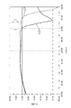
- FIG. 6 is a diagram showing characteristics of antennas according to the example and the comparative example.
- the horizontal axis indicates frequency f (GHz).
- the vertical axis indicates gain G (dBi).
- a line L0 indicates the characteristics of the comparative example.
- the comparative example does not have the connection conductor 11 .
- Lines L1, L3, L5 and L7 show the characteristics of four embodiments with different numbers of connection conductors 11.
- FIG. Specifically, the embodiments of lines L1, L3, L5 and L7 have one, three, five and seven connecting conductors 11, respectively. Conditions other than the number of connection conductors 11 are the same in the comparative example and the four examples.
- connection conductors 11 are arranged in the arrangements illustrated in FIGS. 3, 4A, and 4B.
- the number of connection conductors 11 is five, the two connection conductors 11 on both sides in the y direction are eliminated from the embodiment in which the number of connection conductors 11 is seven.
- connection conductor 11 expands the range of frequencies in which the gain is relatively high to the high frequency side. That is, widening of the band is realized.
- the greater the number of connection conductors 11 from another point of view, the longer the connection region RC in the y direction), the greater the effect of widening the band.
- connection conductors 11 when the number of connection conductors 11 is seven (from another point of view, when the connection region RC extends over substantially the entire length of the feeding element 5 in the y direction), a part of the band (28 GHz to 29 GHz ), the gain is slightly reduced.
- the distance from the connection conductors 11 on both sides to the edge 5b of the feeding element 5 in the y direction is the length of the feeding element 5 in the x direction (1/2 ⁇ g ) is about 1/20 (less than 1/10).
- the distance from the connecting conductors 11 on both sides to the edge 5b is about 1/5 (1/10 or more) of the length of the feeding element 5 in the x direction. Therefore, if all of the connection conductor 11 (in other words, the connection region RC) is separated from the edge portion 5b by a distance of 1/10 or more of the length of the feeding element 5 in the x direction, the above gain can be obtained. It can be said that the probability of occurrence of a decrease is reduced.
- FIG. 7 is a diagram showing characteristics of antennas according to the example and the comparative example.
- the horizontal axis indicates frequency f (GHz).
- the vertical axis indicates the reflection coefficient ⁇ (dB).
- 8 is a diagram showing a part of FIG. 7.
- lines L0, L1, L3, L5, and L7 show the characteristics of comparative examples or examples in which the number of connection conductors 11 is 0, 1, 3, 5, and 7, as in FIG. .
- a first resonance point RF1 and a second resonance point RF2 appear, as indicated by dotted lines in FIG. Then, as shown in FIG. 7, the first resonance points RF1 of the comparative example and the four examples appear at substantially the same frequency.
- the second resonance point RF2 is located on the high frequency side as the number of connection conductors 11 increases. From this, it can be seen that the connection conductor 11 shifts the second resonance point RF2 to the high frequency side to achieve a wide band.
- the third resonance point (reference numeral omitted) occurs in the range of 28 GHz to 29 GHz. It can be seen that the decrease in gain in the above frequency range in FIG. 6 is the effect of this third resonance point.
- 9A and 9B are plan views schematically showing the electric field distribution obtained in the above simulation calculation.
- FIG. 9A shows the electric field distribution according to the comparative example.
- FIG. 9B shows the electric field distribution according to an example in which the number of connection conductors 11 is three.
- the first electric field region EF1 indicates a region in which the electric field intensity fluctuates greatly at the frequency of the first resonance point RF1.
- a second electric field region EF2 indicates a region in which the electric field intensity fluctuates greatly at the frequency of the second resonance point RF2.
- the shape of a part of the actual electric field distribution is simplified and the shape of another part is exaggerated.
- the first electric field region EF1 was a region extending along both edges 5a of the feeding element 5 in the x direction (edges 7a of the parasitic element 7). Also, the position and range did not change significantly between the comparative example and the working example.
- the second electric field region EF2 was a region extending from the edge 5a of the feeding element 5 to the central side of the feeding element 5. Also, the position and range differed between the comparative example and the working example. Specifically, in the example, the width of the second electric field region EF2 was reduced on the central side in the x direction compared to the comparative example. In other words, the length of the second electric field region EF2 in the x direction is shortened.
- connection conductor 11 reduces the length of the second electric field region EF2 in the x direction, thereby shifting the second resonance point RF2 to the high frequency side.
- the antenna 1 has the reference potential layer 3 , the feeding element 5 , the parasitic element 7 , and at least one connecting conductor 11 .
- the reference potential layer 3 extends along a first direction (x direction) and a second direction (y direction) orthogonal to the x direction.
- the feeding element 5 is composed of a layered conductor facing the reference potential layer 3 .
- the feed element 5 has a first feed point (feed point 17 ) located on one side (+x side) in the x direction from the center of the feed element 5 in the x direction.
- the parasitic element 7 is composed of a layered conductor facing the feeding element 5 from the side opposite to the reference potential layer 3 .
- the connection conductor 11 is connected to the feeding element 5 and the parasitic element 7 at a position closer to the center of the feeding element 5 than the feeding point 17 in the x direction, and is electrically connected to the reference potential layer 3 .
- the second resonance point RF2 is shifted to the high frequency side, As a result, the frequency band with high gain can be extended to the high frequency side. That is, it is possible to achieve a wide band.
- the antenna 1 is not intended to discharge due to the grounding of the parasitic element 7, and does not require a conductor for connecting the parasitic element 7 to the reference potential layer 3. In comparison, the configuration is simple.
- the antenna 1 may have a first dielectric layer 15A and a second dielectric layer 15B.
- the first dielectric layer 15A may be interposed between the reference potential layer 3 and the feeding element 5 .
- the second dielectric layer 15B may be interposed between the feed element 5 and the parasitic element 7 .
- At least one connection conductor 11 may include a connection conductor 11 configured by a via conductor penetrating through the second dielectric layer 15B.
- connection conductor 11 can be configured by a known via conductor of a circuit board.
- manufacturing costs are reduced.
- the effective wavelength can be shortened by the dielectric 13 and the size of the antenna 1 can be reduced.
- connection conductors 11 may be positioned within the central length range when the length of the feeding element 5 in the x direction is equally divided into five.
- connection conductor 11 by matching the lengths of the feeding element 5 and the parasitic element 7 in the x direction, multiple resonance is preferably achieved.
- the connection conductor 11 since the position of the connection conductor 11 in the x direction is limited to within 1/5 of the length of the feeding element 5 and the parasitic element 7 in the x direction, the connection conductor 11 is excessively placed in the second electric field region. The probability of interfering with EF2 is reduced. As a result, for example, it is possible to widen the band while reducing the probability of characteristic deterioration caused by the connection conductor 11 .
- the at least one connection conductor 11 may include a plurality of connection conductors 11 whose positions in the y direction are different from each other.
- connection region RC in the y direction from the viewpoint of the manufacturing method.
- All of the plurality of connecting conductors 11 are separated from the edges 5b on both sides of the feeding element 5 in the y direction by a distance of 1/10 or more of the length (1/2 ⁇ g) of the feeding element 5 in the x direction. good.
- the plurality of connection conductors 11 may be arranged at regular intervals in the y direction.
- the contraction of the second electric field region EF2 in the x direction tends to be evenly distributed over the entire length of the connection region RC in the y direction.
- the probability of generating noise due to disturbance of the electric field is reduced.
- Each of the feed element 5 and the parasitic element 7 may have a rectangular shape having two sides parallel to the x direction and two sides parallel to the y direction in plan view.
- the plurality of connection conductors 11 may be arranged linearly in the y direction within the central length range when the length of the feeding element 5 in the x direction is equally divided into five.
- connection conductors 11 are arranged in parallel with the edges 5a on both sides of the feeding element 5 in the x direction (the edges 7a on both sides of the parasitic element 7 in the x direction).
- the probability that the shape of the second electric field region EF2 whose length in the x direction is reduced by the plurality of connection conductors 11 will be disturbed is reduced.
- the connecting conductor 11 in the x direction is limited to within the range of 1/5 of the length of the feeding element 5 and the parasitic element 7 in the x direction, the connecting conductor 11 is excessively placed in the second electric field region EF2.
- the probability of interference is reduced. As a result, for example, it is possible to widen the band while reducing the probability of deterioration of characteristics due to the provision of the connection conductor 11 .
- the at least one connection conductor 11 may include a connection conductor 11 whose length in the x direction is 1/10 or more of the length of the feeding element 5 in the x direction. From another point of view, the length of the connection region RC in the x direction may be 1/10 or more of the length of the feeding element 5 in the x direction.
- the effect of reducing the length of the second electric field region EF2 in the x direction is likely to be achieved.
- x The magnitude of the directions is minimized.
- the at least one connection conductor may include a connection conductor 11C whose length in the y direction is at least twice the length in the x direction (modification of FIG. 5A).
- FIG. 10 is a perspective view showing the configuration of an antenna 201 according to the second embodiment, and corresponds to FIG.
- FIG. 11 is a perspective plan view of part of the antenna 201 and corresponds to FIG.
- the antenna 201 is configured to be capable of transmitting and/or receiving two types of linearly polarized waves whose vibration directions cross each other (for example, orthogonally).
- One of the two linearly polarized waves has the electric field vibration direction in the x direction, as in the first embodiment.
- the other of the two linearly polarized waves uses the y direction as the electric field oscillation direction, unlike the first embodiment.
- the antenna 201 capable of transmitting and/or receiving two linearly polarized waves as described above can be used, for example, as an antenna capable of transmitting and/or receiving both vertically polarized waves and horizontally polarized waves. Also, for example, antenna 201 can be used to transmit and/or receive circularly polarized waves.
- the antenna 201 has a feeding conductor 9A (feeding point 17A and opening 3a associated therewith) and connection conductors 11A and/or 11B corresponding to linearly polarized waves in the x direction. These are similar to the feed conductor 9 and the connection conductor 11 of the antenna 1 . Further, the antenna 201 has a feeding conductor 9B (feeding point 17B and opening 3a associated therewith) and connection conductors 11B and/or 11A, corresponding to linearly polarized waves in the y direction. These are also the same as the feed conductor 9 and connection conductor 11 of the antenna 1, except that the x-direction and y-direction have opposite meanings. Note that A and B may be omitted below.
- the feed element 5 and the parasitic element 7 are squares that match each other when viewed through the plane.
- the feed conductor 9A and the connection conductor 11A, and the feed conductor 9B and the connection conductor 11B are in line symmetry with respect to the diagonal line LD of the feed element 5 (parasitic element 7).
- a straight line (not shown) connecting the power supply conductor 9A and the connection conductor 11A and a straight line (not shown) connecting the power supply conductor 9B and the connection conductor 11B are, for example, orthogonal, and their intersection is, for example, It is located at the center of the feeding element 5 .
- connection conductor 11A may contribute to either widening the band for the linearly polarized wave in the x direction or the band for the linearly polarized wave in the y direction, or may contribute to both.
- the connection conductor 11A is within the central range when the length of the feeding element 5 in the x direction is divided into three equal parts. However, the connection conductor 11A partially protrudes from the central range when the length of the feeding element 5 in the x direction is divided into five equal parts.
- the connection conductor 11A is positioned at the center of the feeding element 5 in the y direction.
- FIGS. 12 and 13 are diagrams showing characteristics of antennas according to the example and the comparative example, and are diagrams corresponding to FIGS. 6 and 7.
- FIG. 12 and 13 are diagrams showing characteristics of antennas according to the example and the comparative example, and are diagrams corresponding to FIGS. 6 and 7.
- FIG. 12 and 13 are diagrams showing characteristics of antennas according to the example and the comparative example, and are diagrams corresponding to FIGS. 6 and 7.
- a line L20 indicates the characteristics of the comparative example.
- the connection conductors 11A and 11B are removed from the antenna 201.
- FIG. A line L21 indicates the characteristics of the example (antenna 201).
- connection conductor 11A partially protrudes from the central region obtained by dividing the length of the feeding element 5 in the x direction into five equal parts. It has been confirmed that a broadband can be achieved while maintaining
- connection conductors 11 may be one.
- one connection conductor 11 may be arranged at the center of the feeding element 5 .
- three or more connection conductors 11 may be arranged, or connection conductors 11 that are not circular in plan view may be provided.
- Various aspects described in the first embodiment may be applied when the x direction of the first embodiment is equated with the x direction of the second embodiment.
- the x direction of the first embodiment is equated with the y direction of the second embodiment
- various aspects described in the first embodiment may be applied.
- the configuration when focusing on the x direction and the configuration when focusing on the y direction may be different (they may not be rotationally symmetrical or linearly symmetrical).
- the antenna 201 has the reference potential layer 3, the feeding element 5, the parasitic element 7, and at least one connecting conductor 11 (11A and 11B).
- the reference potential layer 3 extends along a first direction (x direction) and a second direction (y direction) orthogonal to the x direction.
- the feeding element 5 is composed of a layered conductor facing the reference potential layer 3 .
- the feeding element 5 has a first feeding point (feeding point 17A) located on one side (+x side) in the x direction of the center of the feeding element 5 in the x direction.
- the parasitic element 7 is composed of a layered conductor facing the feeding element 5 from the side opposite to the reference potential layer 3 .
- the connection conductor 11 is connected to the feeding element 5 and the parasitic element 7 at a position closer to the center of the feeding element 5 than the feeding point 17A in the x direction, and is electrically connected to the reference potential layer 3.
- the feeding element 5 may further have a second feeding point (feeding point 17B) located on one side (+y side) in the y direction.
- the feed element 5 and the parasitic element 7 may each be square.
- the feeding points 17A and 17B may be in a line-symmetrical positional relationship with respect to one diagonal line LD of the square of the feeding element 5 .
- At least one connection conductor 11 (11A and 11B) may be positioned closer to the center of the feeding element 5 than the feeding point 17B in the y direction, and may be arranged symmetrically with respect to the diagonal line LD.
- FIG. 14 is a diagram schematically showing the configuration of an electronic device 51 as an application example of the antenna according to the embodiment.
- the reference numerals of the antenna 1 of the first embodiment are used, but the antenna 201 of the second embodiment may be used in the electronic device 51.
- the electronic device 51 may be of various modes.
- electronic device 51 may be a communication device.
- Examples of communication equipment include mobile terminals, base stations, relay stations, wireless LAN (Local Area Network) base units, satellite positioning system receivers, antenna devices that can be attached to and detached from various electronic devices, radios, televisions, and A vehicle-mounted device of an electronic toll collection system (ETC) can be mentioned.
- Mobile terminals include, for example, mobile phones (including smart phones), tablet PCs (Personal Computers), and notebook PCs.
- examples of the electronic device 51 other than the communication device include a radar device and a microwave oven. In addition, below, the description may be made on the premise that the electronic device 51 is a communication device.
- the electronic device 51 has, for example, an antenna module 53 and a housing 55 that houses the antenna module 53 .
- the antenna module 53 has, for example, an antenna 1, a transmission circuit that transmits radio waves via the antenna 1, and/or a reception circuit that receives radio waves via the antenna 1.
- Such transmission circuitry and/or reception circuitry may be configured by one or more ICs 57, for example.
- the IC 57 is, for example, an RF (Radio Frequency)-IC and is electrically connected to the lower end of the feed conductor 9 .
- the transmission circuit may, for example, increase the frequency and modulate a baseband signal containing arbitrary information, and input a high-frequency signal to the antenna 1 (more specifically, the feed conductor 9).
- the transmission circuit selectively feeds power to, for example, two feed conductors 9 (from another point of view, two feed points 17). may selectively transmit two linearly polarized waves. More specifically, for example, the transmission circuit may alternately output two linearly polarized waves at a predetermined cycle. Alternatively, only one of the two linearly polarized waves may be transmitted at all times (until the setting is changed) according to user settings.
- the transmitter circuit may supply currents 90° out of phase to the two feed conductors 9 so that circularly polarized waves are transmitted.
- the receiving circuit may, for example, perform frequency reduction and demodulation on the high-frequency signal from the antenna 1 to obtain a baseband signal containing arbitrary information.
- the receiving circuit selectively utilizes currents from, for example, two feeding conductors 9 (from another point of view, two feeding points 17). you can More specifically, for example, the receiver circuit may always (until the setting is changed) perform the above processing (demodulation, etc.) on only one of the two currents according to the setting by the user. Alternatively, the receiving circuit may perform the above processing only for the larger of the currents from the two feed conductors 9 . Different from the above, the receiving circuit may perform processing similar to that of a receiving circuit that receives circularly polarized waves for the currents from the two feed conductors 9 .
- a specific connection mode between the IC 57 (transmitting circuit and/or receiving circuit) and the antenna 1 is arbitrary.
- the antenna 1 is configured as part of one main surface of the antenna substrate 59 .
- IC 57 is mounted on the other main surface of antenna substrate 59 .
- the feeding conductor 9 is electrically connected to the IC 57 via conductors (conductor layers and/or vias) in the antenna substrate 59 .
- the antenna module 53 has a mounting board 61 on which the antenna board 59 is mounted and electronic components 63 mounted on the mounting board 61 in addition to the antenna board 59 and the IC 57 .
- the IC 57 (transmitting circuit and/or receiving circuit) may be a component mounted on the mounting board 61 .
- the material, size and shape of the electronic device 51 are arbitrary.
- the relative sizes of the antenna 1 and the electronic device 51 are also arbitrary.
- connection conductor 11 may be electrically connected to the reference potential layer 3 .
- various new concepts can be extracted from the present disclosure without requiring that the connection conductor 11 is electrically connected to the reference potential layer 3 .
- the antenna 1 may include a plurality of connection conductors 11 whose positions in the y direction are different from each other, and the x length of the connection conductor 11 is the length of the feed element 5 in the x direction. and that it may be 1/10 or more. From this point of view, a new antenna concept may be extracted, and in this case, it does not matter whether the connection conductor 11 is grounded or not.
- the antenna may not have the dielectric 13 .
- a space from another point of view, air
- the conductor layers may be fixed to each other by, for example, insulating posts.
- the antenna may not have the reference potential layer 3 (ground plane).
- the ground may be used instead of the reference potential layer 3, or a member other than the antenna may be used.
- Other members include, for example, a housing to which the antenna is fixed and a ground layer of a circuit board on which the antenna is mounted. However, in this case, the whole including the housing or the circuit board may be regarded as the antenna.
- the antenna may have components not mentioned in the embodiments.
- a conductor layer having an opening of an appropriate shape may be arranged between the feed element 5 and the parasitic element 7 or above the parasitic element 7 .
- Such a conductor layer functions, for example, as a filter.
- the antenna may be used as an antenna that constitutes an array antenna.
- a plurality of antennas may be arranged along the top surface of the antenna substrate 59.
Landscapes
- Engineering & Computer Science (AREA)
- Microelectronics & Electronic Packaging (AREA)
- Details Of Aerials (AREA)
Priority Applications (2)
| Application Number | Priority Date | Filing Date | Title |
|---|---|---|---|
| JP2023538439A JPWO2023008228A1 (https=) | 2021-07-27 | 2022-07-15 | |
| US18/292,128 US20240339763A1 (en) | 2021-07-27 | 2022-07-15 | Antenna, antenna module, and electronic device |
Applications Claiming Priority (2)
| Application Number | Priority Date | Filing Date | Title |
|---|---|---|---|
| JP2021-122146 | 2021-07-27 | ||
| JP2021122146 | 2021-07-27 |
Publications (1)
| Publication Number | Publication Date |
|---|---|
| WO2023008228A1 true WO2023008228A1 (ja) | 2023-02-02 |
Family
ID=85087602
Family Applications (1)
| Application Number | Title | Priority Date | Filing Date |
|---|---|---|---|
| PCT/JP2022/027832 Ceased WO2023008228A1 (ja) | 2021-07-27 | 2022-07-15 | アンテナ、アンテナモジュール及び電子機器 |
Country Status (3)
| Country | Link |
|---|---|
| US (1) | US20240339763A1 (https=) |
| JP (1) | JPWO2023008228A1 (https=) |
| WO (1) | WO2023008228A1 (https=) |
Families Citing this family (1)
| Publication number | Priority date | Publication date | Assignee | Title |
|---|---|---|---|---|
| US12341256B2 (en) * | 2023-06-29 | 2025-06-24 | National Taiwan University | Dual-polarization cavity-backed antenna, package module, and array package module |
Citations (2)
| Publication number | Priority date | Publication date | Assignee | Title |
|---|---|---|---|---|
| JP2006197188A (ja) * | 2005-01-13 | 2006-07-27 | Anten Corp | アンテナ |
| JP2020025240A (ja) * | 2018-07-31 | 2020-02-13 | パナソニックIpマネジメント株式会社 | アンテナ装置 |
Family Cites Families (2)
| Publication number | Priority date | Publication date | Assignee | Title |
|---|---|---|---|---|
| JPH0998016A (ja) * | 1995-10-02 | 1997-04-08 | Mitsubishi Electric Corp | マイクロストリップアンテナ |
| US11303026B2 (en) * | 2015-12-09 | 2022-04-12 | Viasat, Inc. | Stacked self-diplexed dual-band patch antenna |
-
2022
- 2022-07-15 WO PCT/JP2022/027832 patent/WO2023008228A1/ja not_active Ceased
- 2022-07-15 US US18/292,128 patent/US20240339763A1/en active Pending
- 2022-07-15 JP JP2023538439A patent/JPWO2023008228A1/ja not_active Ceased
Patent Citations (2)
| Publication number | Priority date | Publication date | Assignee | Title |
|---|---|---|---|---|
| JP2006197188A (ja) * | 2005-01-13 | 2006-07-27 | Anten Corp | アンテナ |
| JP2020025240A (ja) * | 2018-07-31 | 2020-02-13 | パナソニックIpマネジメント株式会社 | アンテナ装置 |
Also Published As
| Publication number | Publication date |
|---|---|
| JPWO2023008228A1 (https=) | 2023-02-02 |
| US20240339763A1 (en) | 2024-10-10 |
Similar Documents
| Publication | Publication Date | Title |
|---|---|---|
| US11011843B2 (en) | Antenna element, antenna module, and communication apparatus | |
| KR102614892B1 (ko) | 안테나 유닛 및 단말 장비 | |
| US10044111B2 (en) | Wideband dual-polarized patch antenna | |
| CN110854529B (zh) | 一种基于平面结构的紧凑型低耦合三极化mimo天线 | |
| EP4053998A1 (en) | Antenna module and electronic device | |
| US20260031540A1 (en) | Antenna, antenna array, and electronic device | |
| CN111129704B (zh) | 一种天线单元和电子设备 | |
| CN111129712B (zh) | 5g毫米波双极化天线模组及手持设备 | |
| US20200203851A1 (en) | Multiaxial antenna, wireless communication module, and wireless communication device | |
| WO2020158810A1 (ja) | 平面アンテナ、平面アレイアンテナ、多軸アレイアンテナ、無線通信モジュールおよび無線通信装置 | |
| US8614649B2 (en) | Antenna and communication device including the same | |
| CN113036403B (zh) | 电子装置及其天线结构 | |
| CN112350051A (zh) | 多频段天线和多频段天线的设计方法 | |
| EP4290687B1 (en) | Wireless communication structure, display panel and wireless communication device | |
| WO2020014874A1 (zh) | 一种集成电路和终端设备 | |
| US20200373666A1 (en) | Multiband antenna, wireless communication module, and wireless communication device | |
| CN118281550A (zh) | 一种基于超表面的5g毫米波微基站天线及天线阵列 | |
| WO2023008228A1 (ja) | アンテナ、アンテナモジュール及び電子機器 | |
| WO2021083219A1 (zh) | 天线单元及电子设备 | |
| WO2022181471A1 (ja) | アンテナ、アンテナモジュール及び電子機器 | |
| CN110518340A (zh) | 一种天线单元及终端设备 | |
| US12537309B2 (en) | Antenna structure and antenna array | |
| CN110808454B (zh) | 一种天线单元及电子设备 | |
| WO2021083217A1 (zh) | 天线单元及电子设备 | |
| CN210576433U (zh) | 一种天线单元及电子设备 |
Legal Events
| Date | Code | Title | Description |
|---|---|---|---|
| 121 | Ep: the epo has been informed by wipo that ep was designated in this application |
Ref document number: 22849291 Country of ref document: EP Kind code of ref document: A1 |
|
| WWE | Wipo information: entry into national phase |
Ref document number: 2023538439 Country of ref document: JP |
|
| NENP | Non-entry into the national phase |
Ref country code: DE |
|
| 122 | Ep: pct application non-entry in european phase |
Ref document number: 22849291 Country of ref document: EP Kind code of ref document: A1 |