WO2023007642A1 - アンテナ装置 - Google Patents
アンテナ装置 Download PDFInfo
- Publication number
- WO2023007642A1 WO2023007642A1 PCT/JP2021/028017 JP2021028017W WO2023007642A1 WO 2023007642 A1 WO2023007642 A1 WO 2023007642A1 JP 2021028017 W JP2021028017 W JP 2021028017W WO 2023007642 A1 WO2023007642 A1 WO 2023007642A1
- Authority
- WO
- WIPO (PCT)
- Prior art keywords
- dipole antenna
- antenna elements
- dielectric substrate
- antenna device
- metal
- Prior art date
- Legal status (The legal status is an assumption and is not a legal conclusion. Google has not performed a legal analysis and makes no representation as to the accuracy of the status listed.)
- Ceased
Links
Images










Classifications
-
- H—ELECTRICITY
- H01—ELECTRIC ELEMENTS
- H01Q—ANTENNAS, i.e. RADIO AERIALS
- H01Q21/00—Antenna arrays or systems
- H01Q21/06—Arrays of individually energised antenna units similarly polarised and spaced apart
-
- H—ELECTRICITY
- H01—ELECTRIC ELEMENTS
- H01Q—ANTENNAS, i.e. RADIO AERIALS
- H01Q21/00—Antenna arrays or systems
- H01Q21/06—Arrays of individually energised antenna units similarly polarised and spaced apart
- H01Q21/08—Arrays of individually energised antenna units similarly polarised and spaced apart the units being spaced along or adjacent to a rectilinear path
-
- H—ELECTRICITY
- H01—ELECTRIC ELEMENTS
- H01Q—ANTENNAS, i.e. RADIO AERIALS
- H01Q9/00—Electrically-short antennas having dimensions not more than twice the operating wavelength and consisting of conductive active radiating elements
- H01Q9/04—Resonant antennas
- H01Q9/16—Resonant antennas with feed intermediate between the extremities of the antenna, e.g. centre-fed dipole
Definitions
- the present disclosure relates to an antenna device.
- the antenna device described in Patent Document 1 has a tightly coupled dipole antenna (Tightly Coupled Dipole Array).
- a tightly coupled dipole antenna has a plurality of dipole antenna elements arranged on a dielectric substrate. In order to ensure electromagnetic coupling between two adjacent dipole antenna elements, the comb-like tips of each dipole antenna element are meshed with each other.
- the tips between the two adjacent dipole antenna elements may be cut off. Therefore, when trying to mount, for example, two dielectric substrates in which the tips of the dipole antenna elements are cut off from each other, one dielectric substrate An electrical connection could not be re-established between the dipole antenna element on top and the dipole antenna element on the other dielectric substrate.
- An object of the present disclosure is to provide an antenna device capable of cutting a dielectric substrate without cutting a dipole antenna element.
- an antenna device includes a metal plate, a dielectric substrate extending in a direction perpendicular to the metal plate, and a plurality of dipole antenna elements provided on the dielectric substrate. , in the vicinity of mutually adjacent dipole antenna elements among the plurality of dipole antenna elements, and at a distance smaller than the wavelength handled by the plurality of dipole antenna elements from the tips of the adjacent dipole antenna elements. and a metal post.
- the antenna device According to the antenna device according to the present disclosure, it is possible to cut the dielectric substrate without cutting the dipole antenna element.
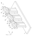
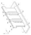
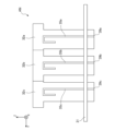
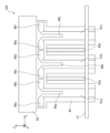
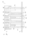
- FIG. 1 is a perspective view of an antenna device AN according to Embodiment 1;
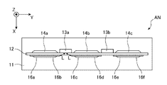
- FIG. 1 is a front view of an antenna device AN according to Embodiment 1;
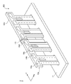
- FIG. 2 is a rear view of the antenna device AN of Embodiment 1.
- FIG. 2 is a top view of the antenna device AN of Embodiment 1.
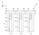
- FIG. 2 is a see-through front view of a dielectric substrate 12 of the antenna device AN of Embodiment 1.
- FIG. 4 is a schematic diagram of current distribution on dipole antenna elements 16a to 16f when metal posts 13a and 13b of Embodiment 1 are not provided.
- FIG. 4 is a schematic diagram of current distribution on dipole antenna elements 16a to 16f when metal posts 13a and 13b of Embodiment 1 are provided.
- FIG. 4 is a schematic diagram of current distribution on dipole antenna elements 16a to 16f when metal posts 13a and 13b of Embodiment 1 are provided.
- FIG. 4 is a perspective view of an antenna device AN according to Modification 1 of Embodiment 1; 3 is a front view of a dielectric substrate 12 of an antenna device AN of Modification 1 of Embodiment 1.
- FIG. FIG. 11 is a perspective view of an antenna device AN according to Modification 2 of Embodiment 1;
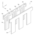
- FIG. 11 is a perspective view of an antenna device AN according to Embodiment 2;
- 8 is an exploded perspective view of a dielectric substrate 22 of the antenna device AN of Embodiment 2.
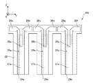
- FIG. 10 is a see-through front view of a dielectric substrate 22 of the antenna device AN of Embodiment 2.
- FIG. FIG. 11 is a perspective view of an antenna device AN according to Embodiment 3;
- FIG. 11 is a front view of an antenna device AN according to Embodiment 3; 11 is a rear view of the antenna device AN of Embodiment 3.
- FIG. FIG. 11 is a perspective view of an antenna device AN provided with a dielectric top plate 50 of Embodiment 4;
- FIG. 11 is a front view of an antenna device AN provided with a dielectric top plate 50 of Embodiment 4;
- FIG. 11 is a perspective view of an antenna device AN provided with a linear conductor 51 of Embodiment 4;
- FIG. 11 is a front view of an antenna device AN provided with a linear conductor 51 of Embodiment 4;
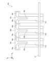
- FIG. 11 is a rear view of an antenna device AN provided with a linear conductor 51 of Embodiment 4; 1 shows a tightly coupled dipole antenna of a conventional antenna device;
- Embodiment 1 The antenna device AN of Embodiment 1 will be described.
- FIG. 1 is a perspective view of the antenna device AN of Embodiment 1.
- FIG. 1 is a perspective view of the antenna device AN of Embodiment 1.
- FIG. 2 is a front view of the antenna device AN of Embodiment 1.
- FIG. 2 is a front view of the antenna device AN of Embodiment 1.
- FIG. 3 is a rear view of the antenna device AN of Embodiment 1.
- FIG. 3 is a rear view of the antenna device AN of Embodiment 1.
- FIG. 4 is a top view of the antenna device AN of Embodiment 1.
- FIG. 4 is a top view of the antenna device AN of Embodiment 1.
- FIG. 5 is a see-through front view of the dielectric substrate 12 of the antenna device AN of Embodiment 1.
- FIG. 5 is a see-through front view of the dielectric substrate 12 of the antenna device AN of Embodiment 1.
- the antenna device AN of Embodiment 1 includes, for example, a metal plate 11, a dielectric substrate 12, and a plurality of metal columns 13a and 13b, as shown in FIG.
- the metal plate 11 corresponds to the "metal plate”
- the dielectric substrate 12 corresponds to the "dielectric substrate”
- the metal columns 13a and 13b correspond to the "metal columns”.
- the metal plate 11 is a rectangular flat plate and parallel to the XY plane.
- the metal plate 11 may have another shape, such as a columnar shape or a polygonal columnar shape, instead of the flat plate shape described above.
- the metal plate 11 is provided with a plurality of openings 14a to 14c penetrating in the Z-axis direction.
- the dielectric substrate 12 is, as shown in FIG. 2, essentially comb-shaped and a single plate.
- Dielectric substrate 12 is divided into a plurality of dielectric substrates 12a-12c as shown in FIG. .
- the dielectric substrates 12a to 12c are each T-shaped when viewed from the X-axis direction.
- the dielectric substrates 12a to 12c are inserted into one of the openings 14a to 14c of the metal plate 11, respectively, and are perpendicular to the metal plate 11, as shown in FIG. It extends in the Z-axis direction.
- a plurality of dipoles are provided at positions corresponding to T-shaped horizontal bars on each of the dielectric substrates 12a to 12c and at positions separated from the metal plate 11 by a predetermined distance H.
- Antenna elements 16a-16f are formed.
- feeder lines 15a-15c are formed at positions corresponding to T-shaped vertical bars on each of dielectric substrates 12a-12c.
- the dipole antenna elements 16a to 16f are connected to the ground conductor 17a of the feeding line 15a, as shown in FIG.
- the ground conductor 17a of the feeder line 15a is formed with a slot 18a that is concave along the Z-axis direction and toward the metal plate 11 (shown in FIG. 1 and the like). there is That is, the slot 18a is electrically connected to the ground conductor 17a.
- the other dipole antenna elements 16c to 16f are also configured in the same manner as the dipole antenna elements 16a and 16b described above.
- the feeder line 15a has an electrically open end as shown in FIG. As shown in FIG. 5, the feeder line 15a receives an input of a high frequency signal RF from a high frequency signal input section 19a.
- a high-frequency signal RF flows in the order of high-frequency signal input section 19a ⁇ feed line 15a ⁇ ground conductor 17a ⁇ dipole antenna elements 16a and 16b.
- the feed line 15a is electromagnetically coupled to the dipole antenna elements 16a and 16b, and excites the dipole antenna elements 16a and 16b.
- the other feeder lines 15b and 15c are also configured in the same manner as the feeder line 15a described above.
- the total length of both the dipole antenna elements 16a and 16b is two times the free space wavelength in the high frequency band in which the antenna device AN should operate in order to radiate radio waves. less than one-tenth of the length.
- the dipole antenna elements 16a, 16b are also balanced antennas. Therefore, the dipole antenna elements 16a and 16b require a balun when excited by the feeder line 15 of unbalanced type (for example, microstrip line).
- the balun is composed of a feed line 15 and a slot 18 .
- the other dipole antenna elements 16c to 16f are also configured in the same manner as the dipole antenna elements 16a and 16b described above.
- the metal columns 13a and 13b extend from the metal plate 11 along the Z-axis direction, as shown in FIG.
- the metal pole 13a is located near the adjacent dipole antenna elements 16b and 16c among the dipole antenna elements 16a to 16f as shown in FIG. As shown in , it is provided at a position facing the dipole antenna elements 16b and 16c with the dielectric substrate 12 interposed therebetween and at a position separated by a distance L from the tip of each of the dipole antenna elements 16b and 16c.
- the distance L is sufficiently smaller than the wavelength of radio waves handled by the dipole antenna elements 16a to 16f.
- a portion of the metal post 13a, a portion of the tip of the dipole antenna element 16b, and a portion of the tip of the dipole antenna element 16c are positioned along the X-axis as shown in FIG. When viewed from the direction, that is, on the YZ plane, they overlap.
- the metal column 13b is also configured in the same manner as the metal column 13a described above.
- the metal posts 13a and 13b are not electrically connected to the dipole antenna elements 16a to 16f in a DC manner. More specifically, as suggested in FIG. 1, the presence of the dielectric substrate 12 allows the metal column 13a to be electrically connected to even the dipole antenna elements 16b and 16c that are in the immediate vicinity of the metal column 13a. Similarly, due to the presence of the dielectric substrate 12, the metal column 13b is not electrically connected even to the dipole antenna elements 16d and 16e that are closest to the metal column 13b.
- FIG. 6 is a schematic diagram of current distribution on the dipole antenna elements 16a to 16f when the metal posts 13a and 13b are not provided.
- FIG. 7 is a schematic diagram of current distribution on dipole antenna elements 16a to 16f when metal posts 13a and 13b are provided.
- FIGS. 6 and 7 show the dielectric substrate 12 after being divided into dielectric substrates 12a, 12b and 12c.
- the current distribution 200 between the dipole antenna elements 16b, 16c is approximately zero near the tips of the dipole antenna elements 16b, 16c, as shown in FIG.
- the vicinity of the resonance frequency of the dipole antenna elements 16b and 16c immediately becomes the operating frequency of the dipole antenna elements 16b and 16c, and the dipole antenna elements 16b and 16c have narrowband characteristics.
- the relationship between the metal post 13b and the other dipole antenna elements 16d and 16e is the same as the relationship between the metal post 13a and the dipole antenna elements 16b and 16c described above.
- the current distribution 300 between the dipole antenna elements 16b, 16c is not zero near the tips of the dipole antenna elements 16b, 16c, as shown in FIG.
- the dipole antenna elements 16b and 16c have a wider band than the characteristics of the dipole antenna elements 16b and 16c when the metal post 13a is not provided. It has a characteristic of less power loss due to
- the relationship between the metal post 13b and the other dipole antenna elements 16d and 16e is the same as the relationship between the metal post 13a and the dipole antenna elements 16b and 16c described above.
- the metal post 13a is arranged between the dipole antenna elements 16b and 16c adjacent to each other with the dielectric substrate 12 interposed to form the dipole antenna element 16b. , 16c.
- the metal column 13a partially overlaps the tips of both the dipole antenna elements 16b and 16c when viewed from the X-axis direction.
- the metal column 13b also has the same configuration as the metal column 13a described above.
- the metal columns 13a and 13b Due to the arrangement of the metal columns 13a and 13b described above, the metal columns 13a are not electrically connected to the dipole antenna elements 16b and 16c in terms of direct current. Similarly, the metal post 13b is also not electrically connected to the dipole antenna elements 16d and 16e in terms of direct current.
- Embodiment 1 in contrast to the conventional art described above, in Embodiment 1, as shown in FIG. Due to the presence of 13a, the electromagnetic coupling between the dipole antenna elements 16b, 16c can be maintained, that is, the electrical connection between the dipole antenna elements 16b, 16c can be maintained. Moreover, the dipole antenna elements 16b, 16c can have the broadband characteristics described above, as described with reference to the current distribution 300 shown in FIG.
- the metal posts 13a and 13b mechanically support the dielectric substrate 12, thereby suppressing the dielectric substrate 12 from overturning toward the XY plane. can be done.
- FIG. 8 is a perspective view of the antenna device AN of Modification 1 of Embodiment 1.
- FIG. 8 is a perspective view of the antenna device AN of Modification 1 of Embodiment 1.
- FIG. 9 is a front view of the dielectric substrate 12 of the antenna device AN of Modification 1 of Embodiment 1.
- FIG. 9 is a front view of the dielectric substrate 12 of the antenna device AN of Modification 1 of Embodiment 1.
- the antenna device AN of Modification 1 uses a balanced feeder line 15a (for example, a microstrip line) as shown in FIGS.
- the feeder lines 15a(1) and 15a(2) of the type for example, coplanar strip lines, planar transmission lines such as parallel strip lines may be used.
- balanced feeding lines 15b(1) and 15b(2) may be used instead of the unbalanced feeding line 15b.
- Balanced feeder lines 15c(1) and 15c(2) may be used instead of the unbalanced feeder line 15c.
- FIG. 10 is a perspective view of the antenna device AN of Modification 2 of Embodiment 1.
- FIG. 10 is a perspective view of the antenna device AN of Modification 2 of Embodiment 1.
- the antenna device AN of Modification 2 is shown in FIG. 10 instead of the dielectric substrate 12a (shown in FIG. 1) provided with a pair of dipole antenna elements 16a and 16b in Embodiment 1, for example. As such, multiple pairs of dipole antenna elements 16a, 16b and another pair of dipole antenna elements 16c, 16d may be provided on the dielectric substrate 12p.
- the other dielectric substrate 12q is similar to the above dielectric substrate 12p.
- the antenna device AN of Modification 2 has the metal column 13, in addition to the same effects as those of the first embodiment, the number of dielectric substrates 12p and 12q is reduced, resulting in more can also be manufactured at low cost.
- Embodiment 2 An antenna device AN according to Embodiment 2 will be described.
- FIG. 11 is a perspective view of the antenna device AN of Embodiment 2.
- FIG. 11 is a perspective view of the antenna device AN of Embodiment 2.
- FIG. 12 is an exploded perspective view of the dielectric substrate 22 of the antenna device AN of Embodiment 2.
- FIG. 12 is an exploded perspective view of the dielectric substrate 22 of the antenna device AN of Embodiment 2.
- FIG. 13 is a see-through front view of the dielectric substrate 22 of the antenna device AN of Embodiment 2.
- the antenna device AN of Embodiment 2 includes a metal plate 21, a dielectric substrate 22, and a plurality of metal columns 23a-23d, as shown in FIGS.
- the antenna device AN of the second embodiment Comparing the antenna device AN of the first embodiment with the antenna device AN of the second embodiment, the antenna device AN of the second embodiment includes the metal plate 21, like the antenna device AN of the first embodiment.
- the antenna device AN of form 1 instead of the dielectric substrate 12, a multilayer dielectric substrate 22 is included, and instead of the two metal pillars 13a, 13b, four metal pillars 23a to 23d are provided. include.
- the dielectric substrate 22 is composed of a dielectric substrate 22a and a dielectric substrate 22b bonded together.
- Dipole antenna elements 26a to 26f are formed inside the dielectric substrate 22, in other words, between the dielectric substrates 22a and 22b, as shown in FIG.
- a plurality of feeder lines 25a to 25c are formed outside the dielectric substrate 22, as shown in FIG.
- Feed lines 25a-25c feed dipole antenna elements 26a-26f, and as shown in FIG. 13, for example, feed line 25a feeds dipole antenna elements 26a, 26b.
- the dielectric substrates 22a and 22b correspond to "first dielectric substrate” and "second dielectric substrate”.
- the metal plate 21 is provided with a plurality of openings 24a-24c, like the plurality of openings 14a-14c of the first embodiment.
- the dielectric substrate 22 is mounted in the openings 24a to 24c and extends in the Z-axis direction in the same manner as the dielectric substrate 12 of the first embodiment.
- the metal columns 23a to 23d extend in the Z-axis direction in the same manner as the metal columns 13a and 13b of the first embodiment.
- the metal posts 23a-23d also partially overlap the tips of the dipole antenna elements 26a-26f, like the metal posts 13a and 13b of the first embodiment.
- the metal posts 23a and 23b partially overlap the tips of the dipole antenna elements 26b and 26c. Part of the tip overlaps.
- metal posts 23a to 23d are arranged on the metal plate 21 at positions sandwiching the dielectric substrate 22, as shown in FIG.
- metal posts 23a and 23b sandwich dielectric substrate 22 between each other, and similarly metal posts 23c and 23d sandwich dielectric substrate 22 between each other.
- the metal pillars 23a and 23b are not electrically connected even to the dipole antenna elements 26b and 26c that are in the immediate vicinity of the metal pillars 23a and 23b. Due to the presence of the dielectric substrate 22, 23c and 23d are not electrically connected to even the dipole antenna elements 26d and 26e that are closest to the metal posts 23c and 23d.
- dipole antenna elements 26 a to 26 f are formed inside dielectric substrate 22 .
- the metal pillars 23a to 23d are DC-electrically connected to the dipole antenna elements 26a to 26f as in the first embodiment.
- two metal posts 23a and 23b instead of one metal post 13a ensure electromagnetic coupling between adjacent dipole antenna elements 26b and 26c
- two metal poles 23c and 23d instead of one metal pole 13b ensure electromagnetic coupling between the adjacent dipole antenna elements 26d and 26e, thereby strengthening the electromagnetic coupling as compared with the first embodiment. can do.
- the dielectric substrate 22 is tilted toward the XY plane in the same manner as the metal columns 13a and 13b of the first embodiment. can be suppressed.
- the feeder lines 25a to 25c may be of a balanced type in place of the unbalanced type as in Modification 1 of Embodiment 1 (shown in FIGS. 8 and 9).
- the dielectric substrate 22 is provided with a pair of dipole antenna elements 26a and 26b in the same manner as in Modification 2 of Embodiment 1 (shown in FIG. 10), instead of providing a plurality of pairs, that is, one pair of dipole antenna elements 26a and 26b. dipole antenna elements 26a, 26b and another pair of dipole antenna elements 26c, 26d may be provided.
- the second modification of the second embodiment can be manufactured at a lower cost than the antenna device AN of the second embodiment, similarly to the second modification of the first embodiment.
- a pair of metal posts 23a and 23b are provided near the pair of dipole antenna elements 26b and 26c, and a pair of metal posts 23c and 23d are provided near the pair of dipole antenna elements 26d and 26e.
- the metal post 23a is provided near the pair of dipole antenna elements 26b and 26c, and near the pair of dipole antenna elements 26d and 26e and diagonally opposite the metal post 23a. Only the metal post 23d may be provided at the position.
- Embodiment 3 An antenna device AN according to Embodiment 3 will be described.
- FIG. 14 is a perspective view of the antenna device AN of Embodiment 3.
- FIG. 14 is a perspective view of the antenna device AN of Embodiment 3.
- FIG. 15 is a front view of the antenna device AN of Embodiment 3.
- FIG. 15 is a front view of the antenna device AN of Embodiment 3.
- FIG. 16 is a rear view of the antenna device AN of Embodiment 3.
- FIG. 16 is a rear view of the antenna device AN of Embodiment 3.
- An antenna device AN of Embodiment 3 includes a metal plate 31 and a plurality of dielectric substrates 32a to 32c, as shown in FIGS.
- the antenna device AN of the third embodiment differs from the antenna device AN of the first embodiment in that it does not include metal poles corresponding to the metal poles 13a and 13b.
- the metal plate 31 is provided with a plurality of openings 34a-34c, similar to the plurality of openings 14a-14c of the first embodiment.
- the openings 34a to 34c are arranged along the Y-axis direction in the same manner as in Embodiment 1 (shown in FIG. 1). are placed in
- the dielectric substrates 32a-32c are inserted into the openings 34a-34c similarly to the dielectric substrates 12a-12c of the first embodiment. Since the openings 34a-34c are staggered or staggered as described above, the dielectric substrates 32a-32c are similarly staggered or staggered. .
- the tips of the adjacent dipole antenna elements 36b and 36c are not electrically connected in a DC manner due to the interposition of the dielectric substrate 32b, and are shown in FIG. As shown, the tips of the dipole antenna elements 36b and 36c partially overlap each other when viewed from the X-axis direction.
- the tips of adjacent dipole antenna elements 36d and 36e are not electrically connected in a DC manner due to the interposition of dielectric substrate 32b, and as shown in FIG. Parts of the tips of 36d and 36e overlap each other when viewed from the X-axis direction.
- the tips of the dipole antenna elements 36b and 36c are separated from each other by a sufficiently small distance compared to the wavelength of radio waves handled by the dipole antenna elements 36a to 36f.
- the tips of the dipole antenna elements 36d and 36e are separated from each other by a distance that is sufficiently smaller than the wavelength of the radio wave.
- Embodiment 3 Other configurations of Embodiment 3, specifically, configurations of feeder lines 35a to 35c, ground conductors 37a to 37c, slots 38a to 38c, high frequency signal input portions 39a to 39c, baluns, etc. shown in FIG. , the configuration of the feeder lines 15a to 15c, the ground conductors 17a to 17c, the slots 18a to 18c, the high frequency signal input portions 19a to 19c, the balun, etc. shown in FIG.
- the dielectric substrates 32a to 32c are alternately arranged along the Y-axis direction. , and the tips of the adjacent dipole antenna elements 36d and 36e are overlapped with each other when viewed from the X-axis direction. In addition, the tips of the dipole antenna elements 36b and 36c and the tips of the dipole antenna elements 36d and 36e are separated by a distance sufficiently smaller than the wavelength of the radio wave.
- the antenna device AN of the third embodiment as in the first and second embodiments, electromagnetic coupling between the adjacent dipole antenna elements 36b and 36c and electromagnetic coupling between the adjacent dipole antenna elements 36d and 36e are achieved. Coupling can be secured.
- the metal poles 13a and 13b of the first embodiment and the metal poles 23a to 23d of the second embodiment are not used. It can be manufactured at a lower cost than the second embodiment.
- the feeder lines 35a to 35c may be of a balanced type in place of the unbalanced type as in Modification 1 of Embodiment 1 (shown in FIGS. 8 and 9).
- ⁇ Modification 2> On each of the dielectric substrates 32a to 32c, for example, on the dielectric substrate 32a, a plurality of pairs, i.e., one pair of dipole antennas, similar to Variation 2 of Embodiment 1 (shown in FIG. 10) Elements 36a, 36b and another pair of dipole antenna elements 36c, 36d may be provided.
- Embodiment 4 An antenna device AN according to Embodiment 4 will be described.
- FIG. 17 is a perspective view of an antenna device AN provided with a dielectric top plate 50 of Embodiment 4.
- FIG. 17 is a perspective view of an antenna device AN provided with a dielectric top plate 50 of Embodiment 4.
- FIG. 18 is a front view of an antenna device AN provided with the dielectric top plate 50 of Embodiment 4.
- FIG. 18 is a front view of an antenna device AN provided with the dielectric top plate 50 of Embodiment 4.
- the antenna device AN of Embodiment 4 includes a metal plate 41, a dielectric substrate 42, and a plurality of metal columns 43a and 43b, similarly to the antenna device AN of Embodiment 1. ,including.
- the antenna device AN of Embodiment 4 differs from the antenna device AN of Embodiment 1 in that it further includes a dielectric top plate 50 .
- the dielectric top plate 50 is provided above the dipole antenna elements 46a to 46f in the dielectric substrate 42 and facing the metal plate 41, as shown in FIG.
- the input impedance of the dipole antenna elements 46a-46f has frequency characteristics.
- the characteristic impedance of free space is a fixed value, ie it has no frequency characteristic.
- the characteristic impedance of the dielectric top plate 50 is inversely proportional to ⁇ r, given that its dielectric constant is ⁇ r.
- the magnitude of the input impedance looking into the free space from the dielectric top plate 50 can be adjusted by changing the thickness and dielectric constant of the dielectric top plate 50 .
- the dipole antenna elements 46a to 46f are adjusted by adjusting the magnitude of the input impedance when the free space is seen from the dielectric top plate 50 so as to match the magnitude of the input impedance of the dipole antenna elements 46a to 46f. , it is possible to operate in a wider band than when the dielectric top plate 50 is not provided.
- the dielectric top plate 50 is provided in the antenna device AN of the fourth embodiment.
- the antenna device AN of Embodiment 3 has the same effects as those of the antenna devices AN of Embodiments 1 to 3.
- the antenna device AN has more It becomes possible to operate in a wide band.
- FIG. 19 is a perspective view of the antenna device AN provided with the linear conductor 51 of the fourth embodiment.
- FIG. 20 is a front view of an antenna device AN provided with a linear conductor 51 according to Embodiment 4.
- FIG. 20 is a front view of an antenna device AN provided with a linear conductor 51 according to Embodiment 4.
- FIG. 21 is a rear view of the antenna device AN provided with the linear conductor 51 of Embodiment 4.
- FIG. 21 is a rear view of the antenna device AN provided with the linear conductor 51 of Embodiment 4.
- another antenna device AN of Embodiment 4 includes a metal plate 41, a dielectric substrate 42, and a plurality of metal pillars, similarly to the antenna device AN of Embodiment 4 described above. 43a, 43b.
- the antenna device AN of Embodiment 4 differs from the antenna device AN of Embodiment 4 described above in that it further includes a plurality of linear conductors 51 .
- the plurality of linear conductors 51 extend in the Z-axis direction above the dipole antenna elements 46a to 46f and face the metal plate 41 in the dielectric substrate .
- the equivalent dielectric constant of the linear conductor 51 is the same as that of the dielectric substrate 42.
- the magnitude of the equivalent dielectric constant of the linear conductor 51 can be adjusted by changing the length and period of the linear conductor 51 .
- radio waves radiated from the dipole antenna elements 46 a to 46 f are concentrated between the plurality of linear conductors 51 . This increases the influence of the dielectric substrate 42 and increases the equivalent dielectric constant of the plurality of linear conductors 51 .
- the plurality of linear conductors 51 are provided integrally with the dielectric substrate 42, unlike the dielectric top plate 50 provided separately from the dielectric substrate 42 described above. Accordingly, in the other antenna device AN of Embodiment 4, unlike the antenna device AN of Embodiment 4 described above, the dielectric top plate 50 and the dielectric top plate 50 that are separate from the dielectric substrate 42 are provided. Since fasteners (not shown in FIGS. 17 and 18) for fixing the antenna device AN are unnecessary, the antenna device AN can be manufactured at a lower cost than the antenna device AN of the fourth embodiment described above.
- the linear conductor 51 is provided in another antenna device AN according to the fourth embodiment. Accordingly, in addition to having the same effect as the antenna device AN of Embodiments 1 to 3, it is different from the antenna device AN of Embodiments 1 to 3 and has the effect of Embodiment 4 described above. As with the antenna device AN, it becomes possible to operate in a wider band. Further, the other antenna device AN of Embodiment 4 can be manufactured at a lower cost than the antenna device AN of Embodiment 4 described above.
- the antenna device according to the present disclosure can be used to maintain electrical connection between cut dipole antenna elements.
Landscapes
- Variable-Direction Aerials And Aerial Arrays (AREA)
Abstract
アンテナ装置(AN)は、金属板(11)と、前記金属板(11)と垂直な方向に延在する誘電体基板(12)と、前記誘電体基板(12)に設けられた複数のダイポールアンテナ素子(16)と、前記複数のダイポールアンテナ素子(16)のうち相互に隣接するダイポールアンテナ素子(16)の近傍に、かつ、前記隣接するダイポールアンテナ素子(16)の先端から、前記複数のダイポールアンテナ素子(16)が取り扱う波長より小さい距離だけ離隔して設けられた金属柱(13)と、を含む。
Description
本開示は、アンテナ装置に関する。
特許文献1に記載されたアンテナ装置は、密結合ダイポールアンテナ(Tightly Coupled Dipole Array)を有する。密結合ダイポールアンテナでは、誘電体基板上に、複数のダイポールアンテナ素子が配置されている。隣接する2つのダイポールアンテナ素子の相互間で電磁結合を確保すべく、各ダイポールアンテナ素子が有する櫛状の先端部は、相互に噛み合っている。
例えば、定尺寸法である上記した誘電体基板をワークサイズに、即ち、製造ラインに合うサイズに裁断すると、上記した隣接する2つのダイポールアンテナ素子間の先端部同士を切断することがある。従って、大型のアンテナ装置(上記したワークサイズより大きいアンテナ装置)に、例えば、前記ダイポールアンテナ素子の先端部同士が切断された2枚の誘電体基板を実装しようとするとき、一方の誘電体基板上のダイポールアンテナ素子と、他方の誘電体基板上のダイポールアンテナ素子との間で、電気的な接続を再び確立することができなかった。
本開示の目的は、ダイポールアンテナ素子を切断することなく、誘電体基板を切断することが可能なアンテナ装置を提供することにある。
上記した課題を解決すべく、本開示に係るアンテナ装置は、金属板と、前記金属板と垂直な方向に延在する誘電体基板と、前記誘電体基板に設けられた複数のダイポールアンテナ素子と、前記複数のダイポールアンテナ素子のうち相互に隣接するダイポールアンテナ素子の近傍に、かつ、前記隣接するダイポールアンテナ素子の先端から、前記複数のダイポールアンテナ素子が取り扱う波長より小さい距離だけ離隔して設けられた金属柱と、を含む。
本開示に係るアンテナ装置によれば、ダイポールアンテナ素子を切断することなく、誘電体基板を切断することが可能となる。
本開示に係るアンテナ装置の実施形態について説明する。
実施形態1.
〈実施形態1〉
実施形態1のアンテナ装置ANについて説明する。
〈実施形態1〉
実施形態1のアンテナ装置ANについて説明する。
〈実施形態1の構成〉
図1は、実施形態1のアンテナ装置ANの斜視図である。
図1は、実施形態1のアンテナ装置ANの斜視図である。
図2は、実施形態1のアンテナ装置ANの正面図である。
図3は、実施形態1のアンテナ装置ANの背面図である。
図4は、実施形態1のアンテナ装置ANの上面図である。
図5は、実施形態1のアンテナ装置ANの誘電体基板12の透視正面図である。
実施形態1のアンテナ装置ANは、例えば、図1に示されるように、金属板11と、誘電体基板12と、複数の金属柱13a、13bと、を含む。
金属板11は、「金属板」に対応し、誘電体基板12は、「誘電体基板」に対応し、金属柱13a、13bは、「金属柱」に対応する。
〈金属板11の構成〉
金属板11は、図1に示されるように、平板状の矩形であり、かつ、XY平面に平行である。金属板11は、上記した平板状に代えて、他の形状、例えば、円柱状、多角柱状でもよい。金属板11には、図1に示されるように、Z軸方向に貫通する複数の開口部14a~14cが、設けられている。
金属板11は、図1に示されるように、平板状の矩形であり、かつ、XY平面に平行である。金属板11は、上記した平板状に代えて、他の形状、例えば、円柱状、多角柱状でもよい。金属板11には、図1に示されるように、Z軸方向に貫通する複数の開口部14a~14cが、設けられている。
〈誘電体基板12の構成〉
誘電体基板12は、図2に示されるように、本来的には、櫛状であり、かつ、一枚の板である。誘電体基板12は、他方で、図2に示されるように、例えば、切断面100a、100bで切断されると、図1に示されるように、複数の誘電体基板12a~12cに分割される。
誘電体基板12は、図2に示されるように、本来的には、櫛状であり、かつ、一枚の板である。誘電体基板12は、他方で、図2に示されるように、例えば、切断面100a、100bで切断されると、図1に示されるように、複数の誘電体基板12a~12cに分割される。
誘電体基板12a~12cは、図1に示されるように、X軸方向から見て、それぞれ、T字状である。誘電体基板12a~12cは、図1に示されるように、それぞれ、金属板11の開口部14a~14cのうちの一つに挿着されており、かつ、金属板11と垂直な方向であるZ軸方向に延在している。
図1に示されるように、誘電体基板12a~12cの各々におけるT字の横棒に相当する位置であり、かつ、金属板11から予め定められた距離Hだけ離れた位置に、複数のダイポールアンテナ素子16a~16fが、形成されている。他方で、図1に示されるように、誘電体基板12a~12cの各々におけるT字の縦棒に相当する位置に、給電線路15a~15cが、形成されている。
ダイポールアンテナ素子16a~16fのうち、例えば、ダイポールアンテナ素子16a、16bは、図5に示されるように、給電線路15aの地導体17aに接続されている。図5に示されるように、給電線路15aの地導体17aには、Z軸方向に沿って、かつ金属板11(図1等に図示。)に向けて凹状であるスロット18aが、形成されている。即ち、スロット18aは、地導体17aに電気的に接続されている。
他のダイポールアンテナ素子16c~16fも、上記したダイポールアンテナ素子16a、16bと同様に構成されている。
給電線路15a~15cのうち、例えば、給電線路15aは、図5に示されるように、先端が電気的に開放されている。給電線路15aは、図5に示されるように、高周波信号入力部19aから、高周波信号RFの入力を受ける。高周波信号RFは、高周波信号入力部19a→給電線路15a→地導体17a→ダイポールアンテナ素子16a、16bの順に流れる。給電線路15aは、ダイポールアンテナ素子16a、16bと電磁結合しており、ダイポールアンテナ素子16a、16bを励振する。
他の給電線路15b、15cも、上記した給電線路15aと同様に構成されている。
ダイポールアンテナ素子16a~16fのうち、例えば、ダイポールアンテナ素子16a、16bの両者を合わせた全長は、電波を放射すべく、アンテナ装置ANが動作すべき帯域である高域周波数における自由空間波長の2分の1以下の長さである。ダイポールアンテナ素子16a、16bは、また、平衡型のアンテナである。従って、ダイポールアンテナ素子16a、16bは、不平衡型(例えば、マイクロストリップ線路)である給電線路15で励振する場合、バランが必要となる。バランは、給電線路15及びスロット18により構成されている。
他のダイポールアンテナ素子16c~16fも、上記したダイポールアンテナ素子16a、16bと同様に構成されている。
〈金属柱13a、13bの構成〉
金属柱13a、13bは、図1に示されるように、金属板11からZ軸方向に沿って延在している。金属柱13a、13bのうち、例えば、金属柱13aは、図1に示されるように、ダイポールアンテナ素子16a~16fのうち、相互に隣接するダイポールアンテナ素子16b、16cの近傍に、かつ、図4に示されるように、誘電体基板12を介在させつつ、ダイポールアンテナ素子16b、16cと対向する位置であって、ダイポールアンテナ素子16b、16cの各々の先端から、距離Lだけ離隔した位置に設けられている。ここで、距離Lは、ダイポールアンテナ素子16a~16fが取り扱う電波の波長に比べて十分に小さい。
金属柱13a、13bは、図1に示されるように、金属板11からZ軸方向に沿って延在している。金属柱13a、13bのうち、例えば、金属柱13aは、図1に示されるように、ダイポールアンテナ素子16a~16fのうち、相互に隣接するダイポールアンテナ素子16b、16cの近傍に、かつ、図4に示されるように、誘電体基板12を介在させつつ、ダイポールアンテナ素子16b、16cと対向する位置であって、ダイポールアンテナ素子16b、16cの各々の先端から、距離Lだけ離隔した位置に設けられている。ここで、距離Lは、ダイポールアンテナ素子16a~16fが取り扱う電波の波長に比べて十分に小さい。
金属柱13aの上記した配置により、金属柱13aの一部と、ダイポールアンテナ素子16bの先端の一部、及びダイポールアンテナ素子16cの先端の一部とは、図1に示されるように、X軸方向から見たとき、即ち、YZ平面上で重なり合う。
金属柱13bも、上記した金属柱13aと同様に構成されている。
金属柱13a、13bは、誘電体基板12の存在により、ダイポールアンテナ素子16a~16fと直流的には電気的接続がされていない。より詳しくは、図1に示唆されるように、金属柱13aは、誘電体基板12の存在により、金属柱13aの直近であるダイポールアンテナ素子16b、16cとさえ直流的には電気的接続がされておらず、同様に、金属柱13bは、誘電体基板12の存在により、金属柱13bの直近であるダイポールアンテナ素子16d、16eとさえ直流的には電接的接続がされていない。
〈金属柱13a、13bの有無による電流分布〉
図6は、金属柱13a、13bが設けられていない場合のダイポールアンテナ素子16a~16f上での電流分布の模式図である。
図6は、金属柱13a、13bが設けられていない場合のダイポールアンテナ素子16a~16f上での電流分布の模式図である。
図7は、金属柱13a、13bが設けられている場合のダイポールアンテナ素子16a~16f上での電流分布の模式図である。
図6及び図7の両者は、誘電体基板12が誘電体基板12a、12b、12cに分割された後を示す。
〈金属柱13a、13bが無い場合〉
例えば、金属柱13aが設けられていない場合における、ダイポールアンテナ素子16b、16cの間の電磁結合は、金属柱13aが設けられている場合における、ダイポールアンテナ素子16b、16cの間の電磁結合と比較して弱い。これにより、ダイポールアンテナ素子16b、16cの先端の両者は、電気的に開放状態である。
例えば、金属柱13aが設けられていない場合における、ダイポールアンテナ素子16b、16cの間の電磁結合は、金属柱13aが設けられている場合における、ダイポールアンテナ素子16b、16cの間の電磁結合と比較して弱い。これにより、ダイポールアンテナ素子16b、16cの先端の両者は、電気的に開放状態である。
上記した開放状態に起因して、ダイポールアンテナ素子16b、16cの間での電流分布200は、図6に示されるように、ダイポールアンテナ素子16b、16cの先端の付近で、概ねゼロである。その結果、ダイポールアンテナ素子16b、16cの共振周波数の付近が、直ちに、ダイポールアンテナ素子16b、16cの動作周波数となり、ダイポールアンテナ素子16b、16cは、狭帯域な特性を有することになる。
金属柱13b及び他のダイポールアンテナ素子16d、16e間の関係は、上記した、金属柱13a及びダイポールアンテナ素子16b、16c間の関係と同様である。
〈金属柱13a、13bがある場合〉
上述とは対照的に、例えば、金属柱13aが設けられている場合における、ダイポールアンテナ素子16b、16cの間の電磁結合は、金属柱13aが設けられていない場合における、ダイポールアンテナ素子16bと、16cの間の電磁結合と比較して強い。これにより、ダイポールアンテナ素子16b、16cの先端の両者は、電磁結合がされている。
上述とは対照的に、例えば、金属柱13aが設けられている場合における、ダイポールアンテナ素子16b、16cの間の電磁結合は、金属柱13aが設けられていない場合における、ダイポールアンテナ素子16bと、16cの間の電磁結合と比較して強い。これにより、ダイポールアンテナ素子16b、16cの先端の両者は、電磁結合がされている。
上記した電磁結合に起因して、ダイポールアンテナ素子16b、16c間での電流分布300は、図7に示されるように、ダイポールアンテナ素子16b、16cの先端の付近で、ゼロではない。その結果、ダイポールアンテナ素子16b、16cは、上記した、金属柱13aが設けられていない場合のダイポールアンテナ素子16b、16cの特性と比して広帯域に亘って、ダイポールアンテナ素子16b、16cからの反射による電力損失が少ない特性を有することになる。
金属柱13b及び他のダイポールアンテナ素子16d、16e間の関係は、上記した、金属柱13a及びダイポールアンテナ素子16b、16c間の関係と同様である。
〈実施形態1の効果〉
上述したように、実施形態1のアンテナ装置ANでは、例えば、金属柱13aが、相互に隣接するダイポールアンテナ素子16b、16cの間に、かつ、誘電体基板12を介在させて、ダイポールアンテナ素子16b、16cと対向する位置に配置されている。
上述したように、実施形態1のアンテナ装置ANでは、例えば、金属柱13aが、相互に隣接するダイポールアンテナ素子16b、16cの間に、かつ、誘電体基板12を介在させて、ダイポールアンテナ素子16b、16cと対向する位置に配置されている。
金属柱13aの上記した配置により、金属柱13aは、X軸方向から見て、ダイポールアンテナ素子16b、16cの両者の先端の一部と重なり合う。
金属柱13bも、上記した金属柱13aと同様な構成を有する。
上記した、金属柱13a、13bの配置により、金属柱13aは、ダイポールアンテナ素子16b、16cと直流的には電気的接続がされていない。同様に、金属柱13bも、ダイポールアンテナ素子16d、16eと直流的には電気的接続がされていない。
ここで、大型のアンテナ装置ANTを製造する場合に、従来では、図22に示されるように、誘電体基板1000が、切断面2000で切断されることに伴い、ダイポールアンテナ素子1001a、1001b間の接続が切断され、ダイポールアンテナ素子1001a、1001b間で電気的な接続を再び確立することができない。
上記した従来とは対照的に、実施形態1では、図2に示されるように、誘電体基板12が、ダイポールアンテナ素子16b、16c間で、例えば、切断面100aで切断されても、金属柱13aの存在により、ダイポールアンテナ素子16b、16c間の電磁結合を維持することができ、即ち、ダイポールアンテナ素子16b、16c間での電気的な接続を維持することができる。しかも、ダイポールアンテナ素子16b、16cは、図7に図示の電流分布300を参照して説明したように、上記した広帯域特性を有することができる。
金属柱13a、13bが、上記した電磁結合を維持することに加えて、誘電体基板12を機構的に支持することから、誘電体基板12が、XY平面に向けて転倒することを抑制することができる。
〈変形例1〉
図8は、実施形態1の変形例1のアンテナ装置ANの斜視図である。
図8は、実施形態1の変形例1のアンテナ装置ANの斜視図である。
図9は、実施形態1の変形例1のアンテナ装置ANの誘電体基板12の正面図である。
変形例1のアンテナ装置ANは、実施形態1のアンテナ装置ANが不平衡型(例えば、マイクロストリップ線路)である給電線路15aを用いることに代えて、図8、9に示されるように、平衡型(例えば、コプレーナストリップ線路、パラレルストリップ線路である平面型伝送線路)である給電線路15a(1)、15a(2)を用いてもよい。
変形例1のアンテナ装置ANは、上記したと同様に、不平衡型である給電線路15bに代えて、平衡型である給電線路15b(1)、15b(2)を用いてもよく、また、不平衡型である給電線路15cに代えて、平衡型である給電線路15c(1)、15c(2)を用いてもよい。
〈変形例2〉
図10は、実施形態1の変形例2のアンテナ装置ANの斜視図である。
変形例2のアンテナ装置ANは、実施形態1における、例えば、誘電体基板12a(図1に図示。)に、一対のダイポールアンテナ素子16a、16bが設けられることに代えて、図10に示されるように、誘電体基板12pに、複数の対、即ち、一の一対のダイポールアンテナ素子16a、16b、及び、他の一対のダイポールアンテナ素子16c、16dが設けられてもよい。
他の誘電体基板12qも、上記の誘電体基板12pと同様である。
変形例2のアンテナ装置ANでは、金属柱13を有することから、実施形態1と同様な効果に加えて、誘電体基板12p、12qの枚数を削減することにより、実施形態1のアンテナ装置ANよりも安価に製造することができる。
実施形態2.
〈実施形態2〉
実施形態2のアンテナ装置ANについて説明する。
〈実施形態2の構成〉
図11は、実施形態2のアンテナ装置ANの斜視図である。
〈実施形態2〉
実施形態2のアンテナ装置ANについて説明する。
〈実施形態2の構成〉
図11は、実施形態2のアンテナ装置ANの斜視図である。
図12は、実施形態2のアンテナ装置ANの誘電体基板22の分解斜視図である。
図13は、実施形態2のアンテナ装置ANの誘電体基板22の透視正面図である。
実施形態2のアンテナ装置ANは、図11~図13に示されるように、金属板21と、誘電体基板22と、複数の金属柱23a~23dを含む。
実施形態1のアンテナ装置ANと実施形態2のアンテナ装置ANとを比較すると、実施形態2のアンテナ装置ANは、実施形態1のアンテナ装置ANと同様に、金属板21を含み、他方で、実施形態1のアンテナ装置ANと相違して、誘電体基板12に代えて、多層である誘電体基板22を含み、また、2つの金属柱13a、13bに代えて、4つの金属柱23a~23dを含む。
〈誘電体基板22の構成〉
誘電体基板22は、図11、12に示されるように、相互に貼り合さわれた誘電体基板22aと誘電体基板22bとから構成されている。誘電体基板22の内側には、換言すれば、誘電体基板22aと誘電体基板22bとの間には、図12に示されるように、ダイポールアンテナ素子26a~26fが、形成されている。他方で、誘電体基板22の外側には、図13に示されるように、複数の給電線路25a~25cが、形成されている。給電線路25a~25cは、ダイポールアンテナ素子26a~26fを給電し、図13に示されるように、例えば、給電線路25aは、ダイポールアンテナ素子26a、26bを給電する。
誘電体基板22は、図11、12に示されるように、相互に貼り合さわれた誘電体基板22aと誘電体基板22bとから構成されている。誘電体基板22の内側には、換言すれば、誘電体基板22aと誘電体基板22bとの間には、図12に示されるように、ダイポールアンテナ素子26a~26fが、形成されている。他方で、誘電体基板22の外側には、図13に示されるように、複数の給電線路25a~25cが、形成されている。給電線路25a~25cは、ダイポールアンテナ素子26a~26fを給電し、図13に示されるように、例えば、給電線路25aは、ダイポールアンテナ素子26a、26bを給電する。
誘電体基板22a、22bは、「第1の誘電体基板」、「第2の誘電体基板」に対応する。
〈金属板21の構成〉
金属板21には、実施形態1の複数の開口部14a~14cと同様に、複数の開口部24a~24cが、設けられている。開口部24a~24cには、図11~図13に示されるように、実施形態1の誘電体基板12と同様に、誘電体基板22が、装着され、かつ、Z軸方向に延在している。
金属板21には、実施形態1の複数の開口部14a~14cと同様に、複数の開口部24a~24cが、設けられている。開口部24a~24cには、図11~図13に示されるように、実施形態1の誘電体基板12と同様に、誘電体基板22が、装着され、かつ、Z軸方向に延在している。
〈金属柱23a~23dの構成〉 金属柱23a~23dは、図11に示されるように、実施形態1の金属柱13a、13bと同様に、Z軸方向に延在している。金属柱23a~23dは、また、図11及び図12から明らかであるように、実施形態1の金属柱13a、13bと同様に、ダイポールアンテナ素子26a~26fの先端の一部と重なり合っている。例えば、X軸方向から見たとき、金属柱23a、23bは、ダイポールアンテナ素子26b、26cの先端の一部と重なり合っており、同様に、金属柱23c、23dは、ダイポールアンテナ素子26d、2eの先端の一部と重なり合っている。
金属柱23a~23dは、図11に示されるように、金属板21上で、誘電体基板22を挟む位置に配置されている。例えば、金属柱23a、23bは、相互間で誘電体基板22を挟み、同様に、金属柱23c、23dは、相互間で誘電体基板22を挟む。
金属柱23a、23bは、誘電体基板22の存在により、金属柱23a、23bの直近であるダイポールアンテナ素子26b、26cとでさえ直流的に電気的接続がされておらず、同様に、金属柱23c、23dは、誘電体基板22の存在により、金属柱23c、23dの直近であるダイポールアンテナ素子26d、26eとでさえ直流的に電気的接続がされていない。
〈その他の構成〉
実施形態2のその他の構成、具体的には、図13に図示された、給電線路25a~25c、地導体27a~27c、スロット28a~28c、高周波信号入力部29a~29c、バラン等の構成は、実施形態1で図5等に図示された、給電線路15a~15c、地導体17a~17c、スロット18a~18c、高周波信号入力部19a~19c、バラン等の構成と同様である。
実施形態2のその他の構成、具体的には、図13に図示された、給電線路25a~25c、地導体27a~27c、スロット28a~28c、高周波信号入力部29a~29c、バラン等の構成は、実施形態1で図5等に図示された、給電線路15a~15c、地導体17a~17c、スロット18a~18c、高周波信号入力部19a~19c、バラン等の構成と同様である。
〈実施形態2の効果〉
実施形態2のアンテナ装置ANでは、ダイポールアンテナ素子26a~26fが、誘電体基板22の内部に形成されている。これにより、金属柱23a~23dが、誘電体基板22の表面と接触しても、実施形態1と同様に、金属柱23a~23dは、ダイポールアンテナ素子26a~26fとは直流的に電気的接続がされることなく、かつ、実施形態1と相違し、1つの金属柱13aに代えて2つの金属柱23a、23bにより、隣接するダイポールアンテナ素子26b、26c間での電磁結合を確保し、かつ、1つの金属柱13bに代えて2つの金属柱23c、23dにより、隣接するダイポールアンテナ素子26d、26e間での電磁結合を確保することによって、実施形態1に比して、電磁結合をより強化することができる。
実施形態2のアンテナ装置ANでは、ダイポールアンテナ素子26a~26fが、誘電体基板22の内部に形成されている。これにより、金属柱23a~23dが、誘電体基板22の表面と接触しても、実施形態1と同様に、金属柱23a~23dは、ダイポールアンテナ素子26a~26fとは直流的に電気的接続がされることなく、かつ、実施形態1と相違し、1つの金属柱13aに代えて2つの金属柱23a、23bにより、隣接するダイポールアンテナ素子26b、26c間での電磁結合を確保し、かつ、1つの金属柱13bに代えて2つの金属柱23c、23dにより、隣接するダイポールアンテナ素子26d、26e間での電磁結合を確保することによって、実施形態1に比して、電磁結合をより強化することができる。
金属柱23a~23dは、誘電体基板22を挟み込むことにより、上記した電磁結合に加えて、実施形態1の金属柱13a、13bと同様に、誘電体基板22が、XY平面に向けて転倒することを抑制することができる。
〈変形例1〉
給電線路25a~25cは、非平衡型に代えて、実施形態1の変形例1(図8、図9に図示。)と同様に、平衡型であってもよい。
給電線路25a~25cは、非平衡型に代えて、実施形態1の変形例1(図8、図9に図示。)と同様に、平衡型であってもよい。
〈変形例2〉
誘電体基板22には、実施形態1の変形例2(図10に図示。)と同様に、一対のダイポールアンテナ素子26a、26bが設けられることに代えて、複数の対、即ち、一の一対のダイポールアンテナ素子26a、26b、及び、他の一対のダイポールアンテナ素子26c、26dが設けられてもよい。実施形態2の変形例2では、実施形態1の変形例2と同様に、実施形態2のアンテナ装置ANよりも安価に製造することができる。
誘電体基板22には、実施形態1の変形例2(図10に図示。)と同様に、一対のダイポールアンテナ素子26a、26bが設けられることに代えて、複数の対、即ち、一の一対のダイポールアンテナ素子26a、26b、及び、他の一対のダイポールアンテナ素子26c、26dが設けられてもよい。実施形態2の変形例2では、実施形態1の変形例2と同様に、実施形態2のアンテナ装置ANよりも安価に製造することができる。
〈変形例3〉
実施形態2における、一対のダイポールアンテナ素子26b、26cの近傍に一対の金属柱23a、23bが設けられ、かつ、一対のダイポールアンテナ素子26d、26eの近傍に一対の金属柱23c、23dが設けられることに代えて、例えば、一対のダイポールアンテナ素子26b、26cの近傍に、金属柱23aのみが設けられ、かつ、一対のダイポールアンテナ素子26d、26eの近傍に、かつ、金属柱23aの斜向かいの位置に、金属柱23dのみが設けられてもよい。
実施形態2における、一対のダイポールアンテナ素子26b、26cの近傍に一対の金属柱23a、23bが設けられ、かつ、一対のダイポールアンテナ素子26d、26eの近傍に一対の金属柱23c、23dが設けられることに代えて、例えば、一対のダイポールアンテナ素子26b、26cの近傍に、金属柱23aのみが設けられ、かつ、一対のダイポールアンテナ素子26d、26eの近傍に、かつ、金属柱23aの斜向かいの位置に、金属柱23dのみが設けられてもよい。
実施形態3.
〈実施形態3〉
実施形態3のアンテナ装置ANについて説明する。
〈実施形態3〉
実施形態3のアンテナ装置ANについて説明する。
〈実施形態3の構成〉
図14は、実施形態3のアンテナ装置ANの斜視図である。
図14は、実施形態3のアンテナ装置ANの斜視図である。
図15は、実施形態3のアンテナ装置ANの正面図である。
図16は、実施形態3のアンテナ装置ANの背面図である。
実施形態3のアンテナ装置ANは、図14~図16に示されるように、金属板31と、複数の誘電体基板32a~32cと、を含む。実施形態3のアンテナ装置ANは、実施形態1のアンテナ装置ANと相違し、金属柱13a、13bに相当する金属柱を含まない。
〈金属板31の構成〉
金属板31には、図14に示されるように、実施形態1の複数の開口部14a~14cと同様に、複数の開口部34a~34cが、設けられている。開口部34a~34cは、実施形態1と同様に(図1に図示。)、Y軸方向に沿って配置されており、他方で、実施形態1と相違して、千鳥状に、即ち、互い違いに配置されている。
金属板31には、図14に示されるように、実施形態1の複数の開口部14a~14cと同様に、複数の開口部34a~34cが、設けられている。開口部34a~34cは、実施形態1と同様に(図1に図示。)、Y軸方向に沿って配置されており、他方で、実施形態1と相違して、千鳥状に、即ち、互い違いに配置されている。
〈誘電体基板32a~32cの構成〉
誘電体基板32a~32cは、図14に示されるように、実施形態1の誘電体基板12a~12cと同様に、開口部34a~34cに挿入されている。開口部34a~34cが、上述したように、千鳥状に、即ち、互い違いに配置されていることから、誘電体基板32a~32cも、同様に、千鳥状に、即ち、互い違いに配置されている。
誘電体基板32a~32cは、図14に示されるように、実施形態1の誘電体基板12a~12cと同様に、開口部34a~34cに挿入されている。開口部34a~34cが、上述したように、千鳥状に、即ち、互い違いに配置されていることから、誘電体基板32a~32cも、同様に、千鳥状に、即ち、互い違いに配置されている。
ダイポールアンテナ素子36a~36fのうち、例えば、隣接するダイポールアンテナ素子36b、36cの先端同士は、誘電体基板32bの介在により、直流的には電気的に接続されておらず、かつ、図14に示されるように、ダイポールアンテナ素子36b、36cの先端の一部同士は、X軸方向から見て、相互に重ね合っている。
同様に、隣接するダイポールアンテナ素子36d、36eの先端同士は、誘電体基板32bの介在により、直流的には電気的に接続されておらず、かつ、図14に示されるように、ダイポールアンテナ素子36d、36eの先端の一部は、X軸方向から見て、相互に重ね合っている。
上記に加えて、ダイポールアンテナ素子36b、36cの先端同士は、ダイポールアンテナ素子36a~36fが取り扱う電波の波長に比べて十分に小さい距離だけ離隔している。同様に、ダイポールアンテナ素子36d、36eの先端同士は、上記した電波の波長に比べて十分に小さい距離だけ離隔している。
〈その他の構成〉
実施形態3のその他の構成、具体的には、図15に図示された、給電線路35a~35c、地導体37a~37c、スロット38a~38c、高周波信号入力部39a~39c、バラン等の構成は、実施形態1で図5等に図示された、給電線路15a~15c、地導体17a~17c、スロット18a~18c、高周波信号入力部19a~19c、バラン等の構成と同様である。
実施形態3のその他の構成、具体的には、図15に図示された、給電線路35a~35c、地導体37a~37c、スロット38a~38c、高周波信号入力部39a~39c、バラン等の構成は、実施形態1で図5等に図示された、給電線路15a~15c、地導体17a~17c、スロット18a~18c、高周波信号入力部19a~19c、バラン等の構成と同様である。
〈実施形態3の効果〉
上述したように、実施形態3のアンテナ装置ANでは、誘電体基板32a~32cがY軸方向に沿って互い違いに配置されており、これにより、隣接するダイポールアンテナ素子36b、36cの先端同士、及び、隣接するダイポールアンテナ素子36d、36eの先端同士が、それぞれ、X軸方向から見て、重ね合わされる。加えて、ダイポールアンテナ素子36b、36cの先端同士は、及び、ダイポールアンテナ素子36d、36eの先端同士は、それぞれ、上記した電波の波長に比べて十分に小さい距離だけ離隔している。
上述したように、実施形態3のアンテナ装置ANでは、誘電体基板32a~32cがY軸方向に沿って互い違いに配置されており、これにより、隣接するダイポールアンテナ素子36b、36cの先端同士、及び、隣接するダイポールアンテナ素子36d、36eの先端同士が、それぞれ、X軸方向から見て、重ね合わされる。加えて、ダイポールアンテナ素子36b、36cの先端同士は、及び、ダイポールアンテナ素子36d、36eの先端同士は、それぞれ、上記した電波の波長に比べて十分に小さい距離だけ離隔している。
これにより、実施形態3のアンテナ装置ANでは、実施形態1及び実施形態2と同様に、隣接するダイポールアンテナ素子36b、36c間での電磁結合、及び隣接するダイポールアンテナ素子36d、36e間での電磁結合を確保することができる。実施形態3のアンテナ装置ANでは、前記した電磁結合を確保する効果に加えて、実施形態1の金属柱13a、13b及び実施形態2の金属柱23a~23dを用いないことから、実施形態1及び実施形態2に比して安価に製造することができる。
〈変形例1〉
給電線路35a~35cは、非平衡型に代えて、実施形態1の変形例1(図8、図9に図示。)と同様に、平衡型であってもよい。
〈変形例2〉
誘電体基板32a~32cの各々には、例えば、誘電体基板32aには、実施形態1の変形例2(図10に図示。)と同様に、複数の対、即ち、一の対のダイポールアンテナ素子36a、36b、及び他の対のダイポールアンテナ素子36c、36dが設けられてもよい。
給電線路35a~35cは、非平衡型に代えて、実施形態1の変形例1(図8、図9に図示。)と同様に、平衡型であってもよい。
〈変形例2〉
誘電体基板32a~32cの各々には、例えば、誘電体基板32aには、実施形態1の変形例2(図10に図示。)と同様に、複数の対、即ち、一の対のダイポールアンテナ素子36a、36b、及び他の対のダイポールアンテナ素子36c、36dが設けられてもよい。
実施形態4.
〈実施形態4〉
実施形態4のアンテナ装置ANについて説明する。
〈実施形態4〉
実施形態4のアンテナ装置ANについて説明する。
〈実施形態4の構成〉
図17は、実施形態4の誘電体天板50を設けたアンテナ装置ANの斜視図である。
図17は、実施形態4の誘電体天板50を設けたアンテナ装置ANの斜視図である。
図18は、実施形態4の誘電体天板50を設けたアンテナ装置ANの正面図である。
実施形態4のアンテナ装置ANは、図17、図18に示されるように、実施形態1のアンテナ装置ANと同様に、金属板41と、誘電体基板42と、複数の金属柱43a、43bと、を含む。実施形態4のアンテナ装置ANは、他方で、実施形態1のアンテナ装置ANと相違し、さらに、誘電体天板50を含む。
〈誘電体天板50の構成〉
誘電体天板50は、図17に示されるように、誘電体基板42中のダイポールアンテナ素子46a~46fの上方に、かつ、金属板41と対向して設けられている。
誘電体天板50は、図17に示されるように、誘電体基板42中のダイポールアンテナ素子46a~46fの上方に、かつ、金属板41と対向して設けられている。
ダイポールアンテナ素子46a~46fの入力インピーダンスは、周波数特性を有する。他方で、自由空間の特性インピーダンスは、固定値であり、即ち、周波数特性を有しない。ダイポールアンテナ素子46a~46fと自由空間との間に誘電体天板50を設けることにより、誘電体天板50から自由空間を見込んだ入力インピーダンスは、周波数特性を有することになる。
誘電体天板50の特性インピーダンスは、その比誘電率がεrであるとすると、√εrに反比例する。誘電体天板50から自由空間を見込んだ入力インピーダンスの大きさを、誘電体天板50の厚み及び誘電率を変えることにより、調整することができる。加えて、ダイポールアンテナ素子46a~46fの入力インピーダンスの大きさに適合するように、誘電体天板50から自由空間を見込んだ入力インピーダンスの大きさを調整することにより、ダイポールアンテナ素子46a~46fを、誘電体天板50が無い場合に比してより広帯域で動作させることが可能となる。
〈その他の構成〉
実施形態4のその他の構成は、実施形態1のその他の構成と同様である。
実施形態4のその他の構成は、実施形態1のその他の構成と同様である。
〈実施形態4の効果〉
上述したように、実施形態4のアンテナ装置ANでは、誘電体天板50が設けられている。実施形態3のアンテナ装置ANは、実施形態1~実施形態3のアンテナ装置ANの効果と同様の効果を有することに加えて、実施形態1~実施形態3のアンテナ装置ANと相違して、より広帯域で動作することが可能となる。
上述したように、実施形態4のアンテナ装置ANでは、誘電体天板50が設けられている。実施形態3のアンテナ装置ANは、実施形態1~実施形態3のアンテナ装置ANの効果と同様の効果を有することに加えて、実施形態1~実施形態3のアンテナ装置ANと相違して、より広帯域で動作することが可能となる。
〈実施形態4の他の構成〉
図19は、実施形態4の線状導体51を設けたアンテナ装置ANの斜視図である。
図19は、実施形態4の線状導体51を設けたアンテナ装置ANの斜視図である。
図20は、実施形態4の線状導体51を設けたアンテナ装置ANの正面図である。
図21は、実施形態4の線状導体51を設けたアンテナ装置ANの背面図である。
実施形態4の他のアンテナ装置ANは、上述した実施形態4のアンテナ装置ANと同様に、図19~図21に示されるように、金属板41と、誘電体基板42と、複数の金属柱43a、43bと、を含む。実施形態4のアンテナ装置ANは、他方で、上述した実施形態4のアンテナ装置ANと相違し、さらに、複数の線状導体51を含む。
〈線状導体51の構成〉
複数の線状導体51は、図19に示されるように、誘電体基板42中で、ダイポールアンテナ素子46a~46fの上方に、かつ、金属板41に対向し、Z軸方向に延在する。
複数の線状導体51は、図19に示されるように、誘電体基板42中で、ダイポールアンテナ素子46a~46fの上方に、かつ、金属板41に対向し、Z軸方向に延在する。
線状導体51に対する電波の通過係数が、誘電体基板42に対する電波の通過係数と概ね同一になると、線状導体51の等価的な比誘電率は、誘電体基板42の誘電率と同一となる。線状導体51の等価的な比誘電率の大きさを、線状導体51の長さ及び周期を変えることにより、調整することができる。
例えば、線状導体51の周期を短くすると、ダイポールアンテナ素子46a~46fから放射された電波は、複数の線状導体51の間に集中する。これにより、誘電体基板42の影響が大きくなり、複数の線状導体51の等価誘電率は、高くなる。
複数の線状導体51は、上述した、誘電体基板42とは別体に設けられた誘電体天板50と相違し、誘電体基板42と同体に設けられる。これにより、実施形態4の他のアンテナ装置ANでは、上述した実施形態4のアンテナ装置ANと相違して、誘電体基板42とは別個である誘電体天板50、及び、誘電体天板50を固定するための留め具(図17、図18に図示せず。)が不要となることから、上述した実施形態4のアンテナ装置ANに比してより安価に製造することができる。
〈その他の構成〉
その他の構成は、実施形態1のその他の構成と同様である。
その他の構成は、実施形態1のその他の構成と同様である。
〈実施形態4の他の効果〉
上述したように、実施形態4の他のアンテナ装置ANでは、線状導体51が設けられている。これにより、実施形態1~実施形態3のアンテナ装置ANの効果と同様の効果を有することに加えて、実施形態1~実施形態3のアンテナ装置ANと相違し、かつ、上述した実施形態4のアンテナ装置ANと同様にして、より広帯域で動作することが可能となる。実施形態4の他のアンテナ装置ANでは、さらに、上述した実施形態4のアンテナ装置ANに比して、安価に製造することができる。
上述したように、実施形態4の他のアンテナ装置ANでは、線状導体51が設けられている。これにより、実施形態1~実施形態3のアンテナ装置ANの効果と同様の効果を有することに加えて、実施形態1~実施形態3のアンテナ装置ANと相違し、かつ、上述した実施形態4のアンテナ装置ANと同様にして、より広帯域で動作することが可能となる。実施形態4の他のアンテナ装置ANでは、さらに、上述した実施形態4のアンテナ装置ANに比して、安価に製造することができる。
本開示の要旨を逸脱しない範囲で、上述した実施形態同士を組み合わせてもよく、また、各実施形態中の構成要素を適宜、削除し、変更し、または、他の構成要素を追加してもよい。
本開示に係るアンテナ装置は、切断されたダイポールアンテナ素子同士間で電気的な接続を維持することに利用することができる。
11 金属板、12 誘電体基板、13a、13b 金属柱、14a~14c 開口部、15a~15c 給電線路、16a~16f ダイポールアンテナ素子、17a~17c 地導体、18a~18c スロット、19a~19c 高周波信号入力部、21 金属板、22 誘電体基板、23a~23d 金属柱、24a~24c 開口部、25a~25c 給電線路、26a~26f ダイポールアンテナ素子、27a~27c 地導体、28a~28c スロット、29a~29c 高周波信号入力部、31 金属板、32a~32c 誘電体基板、34a~34c 開口部、35a~35c 給電線路、36a~36f ダイポールアンテナ素子、37a~37c 地導体、38a~38c スロット、39a~39c 高周波信号入力部、41 金属板、42 誘電体基板、43a、43b 金属柱、44a~44b 開口部、46a~46f ダイポールアンテナ素子、47a~47c 地導体、48a~48c スロット、49a~49c 高周波信号入力部、50 誘電体天板、51 線状導体、100a、100b 切断面、200 電流分布、300 電流分布、1000 誘電体基板、1001a、1001b ダイポールアンテナ素子、2000 切断面、AN アンテナ装置、ANT アンテナ装置、H 距離、L 距離、RF 高周波信号。
Claims (6)
- 金属板と、
前記金属板と垂直な方向に延在する誘電体基板と、
前記誘電体基板に設けられた複数のダイポールアンテナ素子と、
前記複数のダイポールアンテナ素子のうち相互に隣接するダイポールアンテナ素子の近傍に、かつ、前記隣接するダイポールアンテナ素子の先端から、前記複数のダイポールアンテナ素子が取り扱う波長より小さい距離だけ離隔して設けられた金属柱と、
を含むアンテナ装置。 - 金属板と、
前記金属板と垂直な方向に延在する誘電体基板と、
前記誘電体基板に設けられた複数のダイポールアンテナ素子と、を含み、
前記誘電体基板は、前記金属板と平行な方向に沿って配置された第1の誘電体基板及び第2の誘電体基板であって、前記複数のダイポールアンテナ素子のうち相互に隣接するダイポールアンテナ素子の先端同士が、前記複数のダイポールアンテナ素子が取り扱う波長より小さい距離だけ離隔するように設けられた前記第1の誘電体基板及び前記第2の誘電体基板から構成される、
アンテナ装置。 - 前記誘電体基板は、相互に貼り合わされた第1の誘電体基板及び第2の誘電体基板からなり、
前記複数のダイポールアンテナ素子は、前記第1の誘電体基板及び前記第2の誘電体基板の間に設けられている、
請求項1又は請求項2に記載のアンテナ装置。 - 前記複数のダイポールアンテナ素子の上方に、かつ、前記金属板と対向して設けられた誘電体天板をさらに含む、
請求項1又は請求項2に記載のアンテナ装置。 - 前記誘電体基板中において、前記複数のダイポールアンテナ素子の上方で、かつ、前記金属板と対向し前記金属板と垂直な方向へ延在する複数の線状導体をさらに含む、
請求項1又は請求項2に記載のアンテナ装置。 - 前記誘電体基板に形成され、かつ、前記垂直な方向に延在する複数の平衡型または非平衡型の給電線路であって、前記複数のダイポールアンテナ素子を励振するための給電線路をさらに含む、
請求項1又は請求項2に記載のアンテナ装置。
Priority Applications (2)
| Application Number | Priority Date | Filing Date | Title |
|---|---|---|---|
| PCT/JP2021/028017 WO2023007642A1 (ja) | 2021-07-29 | 2021-07-29 | アンテナ装置 |
| JP2022513384A JP7134377B1 (ja) | 2021-07-29 | 2021-07-29 | アンテナ装置 |
Applications Claiming Priority (1)
| Application Number | Priority Date | Filing Date | Title |
|---|---|---|---|
| PCT/JP2021/028017 WO2023007642A1 (ja) | 2021-07-29 | 2021-07-29 | アンテナ装置 |
Publications (1)
| Publication Number | Publication Date |
|---|---|
| WO2023007642A1 true WO2023007642A1 (ja) | 2023-02-02 |
Family
ID=83225915
Family Applications (1)
| Application Number | Title | Priority Date | Filing Date |
|---|---|---|---|
| PCT/JP2021/028017 Ceased WO2023007642A1 (ja) | 2021-07-29 | 2021-07-29 | アンテナ装置 |
Country Status (2)
| Country | Link |
|---|---|
| JP (1) | JP7134377B1 (ja) |
| WO (1) | WO2023007642A1 (ja) |
Cited By (1)
| Publication number | Priority date | Publication date | Assignee | Title |
|---|---|---|---|---|
| USD1105667S1 (en) | 2023-11-27 | 2025-12-09 | Beijing Roborock Technology Co., Ltd. | Floor brush for floor washing appliance |
Citations (3)
| Publication number | Priority date | Publication date | Assignee | Title |
|---|---|---|---|---|
| JP2007060082A (ja) * | 2005-08-23 | 2007-03-08 | Nippon Dengyo Kosaku Co Ltd | 多周波共用アンテナ |
| JP2016082247A (ja) * | 2014-10-09 | 2016-05-16 | 富士通株式会社 | アンテナ装置 |
| US10320088B1 (en) * | 2018-11-13 | 2019-06-11 | The Florida International University Board Of Trustees | Balanced wideband impedance transformer |
-
2021
- 2021-07-29 WO PCT/JP2021/028017 patent/WO2023007642A1/ja not_active Ceased
- 2021-07-29 JP JP2022513384A patent/JP7134377B1/ja active Active
Patent Citations (3)
| Publication number | Priority date | Publication date | Assignee | Title |
|---|---|---|---|---|
| JP2007060082A (ja) * | 2005-08-23 | 2007-03-08 | Nippon Dengyo Kosaku Co Ltd | 多周波共用アンテナ |
| JP2016082247A (ja) * | 2014-10-09 | 2016-05-16 | 富士通株式会社 | アンテナ装置 |
| US10320088B1 (en) * | 2018-11-13 | 2019-06-11 | The Florida International University Board Of Trustees | Balanced wideband impedance transformer |
Cited By (1)
| Publication number | Priority date | Publication date | Assignee | Title |
|---|---|---|---|---|
| USD1105667S1 (en) | 2023-11-27 | 2025-12-09 | Beijing Roborock Technology Co., Ltd. | Floor brush for floor washing appliance |
Also Published As
| Publication number | Publication date |
|---|---|
| JP7134377B1 (ja) | 2022-09-09 |
| JPWO2023007642A1 (ja) | 2023-02-02 |
Similar Documents
| Publication | Publication Date | Title |
|---|---|---|
| US10418708B2 (en) | Wideband antenna | |
| JP5983760B2 (ja) | アレーアンテナ | |
| KR101982028B1 (ko) | 편파 공용 안테나 | |
| EP1456907B1 (en) | Antenna element | |
| US6507321B2 (en) | V-slot antenna for circular polarization | |
| US7106255B2 (en) | Stacked patch antenna and method of operation therefore | |
| JP4135861B2 (ja) | 多素子平面アンテナ | |
| US7417587B2 (en) | Ferrite phase shifter and phase array radar system | |
| US9190732B2 (en) | Antenna device | |
| CN102224637A (zh) | 宽带辐射元件 | |
| JP3234393B2 (ja) | アンテナ装置 | |
| CN109428152A (zh) | 天线部件、车载雷达和汽车 | |
| KR20200035161A (ko) | 어레이 안테나 장치 | |
| JP2017098782A (ja) | アンテナ素子 | |
| JP7134377B1 (ja) | アンテナ装置 | |
| JP2002198707A (ja) | 非可逆回路素子および通信装置 | |
| WO2018180877A1 (ja) | 両偏波送受用アンテナ | |
| JP2002344238A (ja) | 偏波共用平面アンテナ | |
| JP2002252515A (ja) | アンテナ装置 | |
| JP5616167B2 (ja) | 進行波励振アンテナ | |
| CN102934284A (zh) | 具有平面导电元件,其中之一具有槽的天线 | |
| JP3064395B2 (ja) | マイクロストリップアンテナ | |
| JP4444994B2 (ja) | 多素子平面アンテナ | |
| JP2014135556A (ja) | アンテナ装置 | |
| JPH10209743A (ja) | スロット結合型マイクロストリップアンテナ |
Legal Events
| Date | Code | Title | Description |
|---|---|---|---|
| ENP | Entry into the national phase |
Ref document number: 2022513384 Country of ref document: JP Kind code of ref document: A |
|
| 121 | Ep: the epo has been informed by wipo that ep was designated in this application |
Ref document number: 21951844 Country of ref document: EP Kind code of ref document: A1 |
|
| NENP | Non-entry into the national phase |
Ref country code: DE |
|
| 122 | Ep: pct application non-entry in european phase |
Ref document number: 21951844 Country of ref document: EP Kind code of ref document: A1 |