WO2023002278A1 - Procédé de réglage de dispositif d'affichage et système de réglage de dispositif d'affichage - Google Patents
Procédé de réglage de dispositif d'affichage et système de réglage de dispositif d'affichage Download PDFInfo
- Publication number
- WO2023002278A1 WO2023002278A1 PCT/IB2022/056030 IB2022056030W WO2023002278A1 WO 2023002278 A1 WO2023002278 A1 WO 2023002278A1 IB 2022056030 W IB2022056030 W IB 2022056030W WO 2023002278 A1 WO2023002278 A1 WO 2023002278A1
- Authority
- WO
- WIPO (PCT)
- Prior art keywords
- display device
- layer
- light
- data
- correction
- Prior art date
Links
- 238000000034 method Methods 0.000 title claims abstract description 121
- 230000006870 function Effects 0.000 claims abstract description 159
- 238000003384 imaging method Methods 0.000 claims abstract description 119
- 238000012937 correction Methods 0.000 claims description 204
- 230000007547 defect Effects 0.000 claims description 30
- 238000012360 testing method Methods 0.000 claims description 7
- 239000010410 layer Substances 0.000 description 581
- 239000000463 material Substances 0.000 description 118
- 239000004065 semiconductor Substances 0.000 description 73
- 239000000758 substrate Substances 0.000 description 71
- 229920005989 resin Polymers 0.000 description 62
- 239000011347 resin Substances 0.000 description 62
- 238000012545 processing Methods 0.000 description 60
- 238000005401 electroluminescence Methods 0.000 description 49
- 239000000126 substance Substances 0.000 description 40
- 239000012044 organic layer Substances 0.000 description 37
- 238000010586 diagram Methods 0.000 description 25
- 229910052751 metal Inorganic materials 0.000 description 25
- 239000002184 metal Substances 0.000 description 25
- 230000008569 process Effects 0.000 description 25
- 238000002347 injection Methods 0.000 description 20
- 239000007924 injection Substances 0.000 description 20
- 238000004891 communication Methods 0.000 description 18
- 239000011241 protective layer Substances 0.000 description 18
- -1 polyglycerin Polymers 0.000 description 17
- 238000006243 chemical reaction Methods 0.000 description 16
- 150000002894 organic compounds Chemical class 0.000 description 16
- 230000003287 optical effect Effects 0.000 description 15
- 238000004519 manufacturing process Methods 0.000 description 14
- 239000003086 colorant Substances 0.000 description 12
- XLOMVQKBTHCTTD-UHFFFAOYSA-N Zinc monoxide Chemical compound [Zn]=O XLOMVQKBTHCTTD-UHFFFAOYSA-N 0.000 description 11
- 150000001875 compounds Chemical class 0.000 description 11
- 230000002950 deficient Effects 0.000 description 11
- 229910044991 metal oxide Inorganic materials 0.000 description 11
- 150000004706 metal oxides Chemical class 0.000 description 11
- 230000032258 transport Effects 0.000 description 11
- 229910052581 Si3N4 Inorganic materials 0.000 description 10
- VYPSYNLAJGMNEJ-UHFFFAOYSA-N Silicium dioxide Chemical compound O=[Si]=O VYPSYNLAJGMNEJ-UHFFFAOYSA-N 0.000 description 10
- XUIMIQQOPSSXEZ-UHFFFAOYSA-N Silicon Chemical compound [Si] XUIMIQQOPSSXEZ-UHFFFAOYSA-N 0.000 description 10
- QVGXLLKOCUKJST-UHFFFAOYSA-N atomic oxygen Chemical compound [O] QVGXLLKOCUKJST-UHFFFAOYSA-N 0.000 description 10
- 239000003990 capacitor Substances 0.000 description 10
- 239000010949 copper Substances 0.000 description 10
- 230000005525 hole transport Effects 0.000 description 10
- 239000001301 oxygen Substances 0.000 description 10
- 229910052760 oxygen Inorganic materials 0.000 description 10
- 229910052710 silicon Inorganic materials 0.000 description 10
- 239000010703 silicon Substances 0.000 description 10
- HQVNEWCFYHHQES-UHFFFAOYSA-N silicon nitride Chemical compound N12[Si]34N5[Si]62N3[Si]51N64 HQVNEWCFYHHQES-UHFFFAOYSA-N 0.000 description 10
- PXHVJJICTQNCMI-UHFFFAOYSA-N Nickel Chemical group [Ni] PXHVJJICTQNCMI-UHFFFAOYSA-N 0.000 description 9
- 239000012790 adhesive layer Substances 0.000 description 9
- 239000012535 impurity Substances 0.000 description 9
- 238000005259 measurement Methods 0.000 description 9
- 150000004767 nitrides Chemical class 0.000 description 9
- 239000004417 polycarbonate Substances 0.000 description 9
- 229920000515 polycarbonate Polymers 0.000 description 9
- 229910052814 silicon oxide Inorganic materials 0.000 description 9
- IJGRMHOSHXDMSA-UHFFFAOYSA-N Atomic nitrogen Chemical compound N#N IJGRMHOSHXDMSA-UHFFFAOYSA-N 0.000 description 8
- RYGMFSIKBFXOCR-UHFFFAOYSA-N Copper Chemical compound [Cu] RYGMFSIKBFXOCR-UHFFFAOYSA-N 0.000 description 8
- 239000000853 adhesive Substances 0.000 description 8
- 230000001070 adhesive effect Effects 0.000 description 8
- 230000015572 biosynthetic process Effects 0.000 description 8
- 229910052802 copper Inorganic materials 0.000 description 8
- TWNQGVIAIRXVLR-UHFFFAOYSA-N oxo(oxoalumanyloxy)alumane Chemical compound O=[Al]O[Al]=O TWNQGVIAIRXVLR-UHFFFAOYSA-N 0.000 description 8
- 238000003860 storage Methods 0.000 description 8
- 238000012546 transfer Methods 0.000 description 8
- XLYOFNOQVPJJNP-UHFFFAOYSA-N water Substances O XLYOFNOQVPJJNP-UHFFFAOYSA-N 0.000 description 8
- 238000001514 detection method Methods 0.000 description 7
- 229910052738 indium Inorganic materials 0.000 description 7
- APFVFJFRJDLVQX-UHFFFAOYSA-N indium atom Chemical compound [In] APFVFJFRJDLVQX-UHFFFAOYSA-N 0.000 description 7
- 239000004973 liquid crystal related substance Substances 0.000 description 7
- 230000007246 mechanism Effects 0.000 description 7
- UFHFLCQGNIYNRP-UHFFFAOYSA-N Hydrogen Chemical compound [H][H] UFHFLCQGNIYNRP-UHFFFAOYSA-N 0.000 description 6
- 229910052782 aluminium Inorganic materials 0.000 description 6
- 230000004888 barrier function Effects 0.000 description 6
- 230000000052 comparative effect Effects 0.000 description 6
- 239000004020 conductor Substances 0.000 description 6
- 230000007274 generation of a signal involved in cell-cell signaling Effects 0.000 description 6
- 239000001257 hydrogen Substances 0.000 description 6
- 229910052739 hydrogen Inorganic materials 0.000 description 6
- 229910010272 inorganic material Inorganic materials 0.000 description 6
- 239000011159 matrix material Substances 0.000 description 6
- 238000000206 photolithography Methods 0.000 description 6
- 229920000178 Acrylic resin Polymers 0.000 description 5
- 239000004925 Acrylic resin Substances 0.000 description 5
- XMWRBQBLMFGWIX-UHFFFAOYSA-N C60 fullerene Chemical class C12=C3C(C4=C56)=C7C8=C5C5=C9C%10=C6C6=C4C1=C1C4=C6C6=C%10C%10=C9C9=C%11C5=C8C5=C8C7=C3C3=C7C2=C1C1=C2C4=C6C4=C%10C6=C9C9=C%11C5=C5C8=C3C3=C7C1=C1C2=C4C6=C2C9=C5C3=C12 XMWRBQBLMFGWIX-UHFFFAOYSA-N 0.000 description 5
- XAGFODPZIPBFFR-UHFFFAOYSA-N aluminium Chemical compound [Al] XAGFODPZIPBFFR-UHFFFAOYSA-N 0.000 description 5
- 239000003822 epoxy resin Substances 0.000 description 5
- 238000011156 evaluation Methods 0.000 description 5
- 239000011521 glass Substances 0.000 description 5
- 229910000449 hafnium oxide Inorganic materials 0.000 description 5
- WIHZLLGSGQNAGK-UHFFFAOYSA-N hafnium(4+);oxygen(2-) Chemical compound [O-2].[O-2].[Hf+4] WIHZLLGSGQNAGK-UHFFFAOYSA-N 0.000 description 5
- 238000004770 highest occupied molecular orbital Methods 0.000 description 5
- 238000004768 lowest unoccupied molecular orbital Methods 0.000 description 5
- 229920000647 polyepoxide Polymers 0.000 description 5
- 239000002096 quantum dot Substances 0.000 description 5
- 229910052719 titanium Inorganic materials 0.000 description 5
- 239000010936 titanium Substances 0.000 description 5
- 229910052721 tungsten Inorganic materials 0.000 description 5
- 238000007740 vapor deposition Methods 0.000 description 5
- 239000011787 zinc oxide Substances 0.000 description 5
- GYHNNYVSQQEPJS-UHFFFAOYSA-N Gallium Chemical compound [Ga] GYHNNYVSQQEPJS-UHFFFAOYSA-N 0.000 description 4
- XEEYBQQBJWHFJM-UHFFFAOYSA-N Iron Chemical group [Fe] XEEYBQQBJWHFJM-UHFFFAOYSA-N 0.000 description 4
- KDLHZDBZIXYQEI-UHFFFAOYSA-N Palladium Chemical compound [Pd] KDLHZDBZIXYQEI-UHFFFAOYSA-N 0.000 description 4
- RTAQQCXQSZGOHL-UHFFFAOYSA-N Titanium Chemical compound [Ti] RTAQQCXQSZGOHL-UHFFFAOYSA-N 0.000 description 4
- HCHKCACWOHOZIP-UHFFFAOYSA-N Zinc Chemical compound [Zn] HCHKCACWOHOZIP-UHFFFAOYSA-N 0.000 description 4
- 239000000956 alloy Substances 0.000 description 4
- WZJYKHNJTSNBHV-UHFFFAOYSA-N benzo[h]quinoline Chemical class C1=CN=C2C3=CC=CC=C3C=CC2=C1 WZJYKHNJTSNBHV-UHFFFAOYSA-N 0.000 description 4
- XJHCXCQVJFPJIK-UHFFFAOYSA-M caesium fluoride Chemical compound [F-].[Cs+] XJHCXCQVJFPJIK-UHFFFAOYSA-M 0.000 description 4
- 230000000295 complement effect Effects 0.000 description 4
- 238000009792 diffusion process Methods 0.000 description 4
- 230000000694 effects Effects 0.000 description 4
- 229910052733 gallium Inorganic materials 0.000 description 4
- 210000003128 head Anatomy 0.000 description 4
- 238000003702 image correction Methods 0.000 description 4
- 150000002484 inorganic compounds Chemical class 0.000 description 4
- MRELNEQAGSRDBK-UHFFFAOYSA-N lanthanum(3+);oxygen(2-) Chemical compound [O-2].[O-2].[O-2].[La+3].[La+3] MRELNEQAGSRDBK-UHFFFAOYSA-N 0.000 description 4
- 239000007788 liquid Substances 0.000 description 4
- 239000007769 metal material Substances 0.000 description 4
- 239000000203 mixture Substances 0.000 description 4
- 229910052750 molybdenum Inorganic materials 0.000 description 4
- PLDDOISOJJCEMH-UHFFFAOYSA-N neodymium(3+);oxygen(2-) Chemical compound [O-2].[O-2].[O-2].[Nd+3].[Nd+3] PLDDOISOJJCEMH-UHFFFAOYSA-N 0.000 description 4
- 229910052759 nickel Inorganic materials 0.000 description 4
- 229910052757 nitrogen Inorganic materials 0.000 description 4
- 229920006122 polyamide resin Polymers 0.000 description 4
- 229920001721 polyimide Polymers 0.000 description 4
- 239000009719 polyimide resin Substances 0.000 description 4
- 230000001681 protective effect Effects 0.000 description 4
- 239000010937 tungsten Substances 0.000 description 4
- 229910052725 zinc Inorganic materials 0.000 description 4
- 239000011701 zinc Substances 0.000 description 4
- XESMNQMWRSEIET-UHFFFAOYSA-N 2,9-dinaphthalen-2-yl-4,7-diphenyl-1,10-phenanthroline Chemical compound C1=CC=CC=C1C1=CC(C=2C=C3C=CC=CC3=CC=2)=NC2=C1C=CC1=C(C=3C=CC=CC=3)C=C(C=3C=C4C=CC=CC4=CC=3)N=C21 XESMNQMWRSEIET-UHFFFAOYSA-N 0.000 description 3
- DHDHJYNTEFLIHY-UHFFFAOYSA-N 4,7-diphenyl-1,10-phenanthroline Chemical compound C1=CC=CC=C1C1=CC=NC2=C1C=CC1=C(C=3C=CC=CC=3)C=CN=C21 DHDHJYNTEFLIHY-UHFFFAOYSA-N 0.000 description 3
- 229910001111 Fine metal Inorganic materials 0.000 description 3
- ZOKXTWBITQBERF-UHFFFAOYSA-N Molybdenum Chemical group [Mo] ZOKXTWBITQBERF-UHFFFAOYSA-N 0.000 description 3
- BQCADISMDOOEFD-UHFFFAOYSA-N Silver Chemical compound [Ag] BQCADISMDOOEFD-UHFFFAOYSA-N 0.000 description 3
- ATJFFYVFTNAWJD-UHFFFAOYSA-N Tin Chemical group [Sn] ATJFFYVFTNAWJD-UHFFFAOYSA-N 0.000 description 3
- 230000001133 acceleration Effects 0.000 description 3
- 150000001454 anthracenes Chemical class 0.000 description 3
- 150000004982 aromatic amines Chemical class 0.000 description 3
- 150000001716 carbazoles Chemical class 0.000 description 3
- 229910052804 chromium Inorganic materials 0.000 description 3
- 239000011651 chromium Substances 0.000 description 3
- PMHQVHHXPFUNSP-UHFFFAOYSA-M copper(1+);methylsulfanylmethane;bromide Chemical compound Br[Cu].CSC PMHQVHHXPFUNSP-UHFFFAOYSA-M 0.000 description 3
- 238000013461 design Methods 0.000 description 3
- 230000006866 deterioration Effects 0.000 description 3
- AJNVQOSZGJRYEI-UHFFFAOYSA-N digallium;oxygen(2-) Chemical compound [O-2].[O-2].[O-2].[Ga+3].[Ga+3] AJNVQOSZGJRYEI-UHFFFAOYSA-N 0.000 description 3
- 239000000428 dust Substances 0.000 description 3
- 229910001195 gallium oxide Inorganic materials 0.000 description 3
- 239000010931 gold Substances 0.000 description 3
- LNEPOXFFQSENCJ-UHFFFAOYSA-N haloperidol Chemical compound C1CC(O)(C=2C=CC(Cl)=CC=2)CCN1CCCC(=O)C1=CC=C(F)C=C1 LNEPOXFFQSENCJ-UHFFFAOYSA-N 0.000 description 3
- AMGQUBHHOARCQH-UHFFFAOYSA-N indium;oxotin Chemical compound [In].[Sn]=O AMGQUBHHOARCQH-UHFFFAOYSA-N 0.000 description 3
- 238000007689 inspection Methods 0.000 description 3
- 239000002346 layers by function Substances 0.000 description 3
- PQXKHYXIUOZZFA-UHFFFAOYSA-M lithium fluoride Chemical compound [Li+].[F-] PQXKHYXIUOZZFA-UHFFFAOYSA-M 0.000 description 3
- 150000002739 metals Chemical class 0.000 description 3
- 239000011733 molybdenum Chemical group 0.000 description 3
- 229910021421 monocrystalline silicon Inorganic materials 0.000 description 3
- 150000002790 naphthalenes Chemical class 0.000 description 3
- 239000005011 phenolic resin Substances 0.000 description 3
- IEQIEDJGQAUEQZ-UHFFFAOYSA-N phthalocyanine Chemical compound N1C(N=C2C3=CC=CC=C3C(N=C3C4=CC=CC=C4C(=N4)N3)=N2)=C(C=CC=C2)C2=C1N=C1C2=CC=CC=C2C4=N1 IEQIEDJGQAUEQZ-UHFFFAOYSA-N 0.000 description 3
- 229920002037 poly(vinyl butyral) polymer Polymers 0.000 description 3
- 229920000642 polymer Polymers 0.000 description 3
- 239000004800 polyvinyl chloride Substances 0.000 description 3
- 229920000915 polyvinyl chloride Polymers 0.000 description 3
- 150000003222 pyridines Chemical class 0.000 description 3
- 229940083082 pyrimidine derivative acting on arteriolar smooth muscle Drugs 0.000 description 3
- 150000003230 pyrimidines Chemical class 0.000 description 3
- 150000003252 quinoxalines Chemical class 0.000 description 3
- 229910052709 silver Inorganic materials 0.000 description 3
- 239000004332 silver Substances 0.000 description 3
- 239000002356 single layer Substances 0.000 description 3
- 229910052715 tantalum Inorganic materials 0.000 description 3
- 229910052718 tin Inorganic materials 0.000 description 3
- WFKWXMTUELFFGS-UHFFFAOYSA-N tungsten Chemical compound [W] WFKWXMTUELFFGS-UHFFFAOYSA-N 0.000 description 3
- 229910052727 yttrium Inorganic materials 0.000 description 3
- ROFVEXUMMXZLPA-UHFFFAOYSA-N Bipyridyl Chemical class N1=CC=CC=C1C1=CC=CC=N1 ROFVEXUMMXZLPA-UHFFFAOYSA-N 0.000 description 2
- VYZAMTAEIAYCRO-UHFFFAOYSA-N Chromium Chemical compound [Cr] VYZAMTAEIAYCRO-UHFFFAOYSA-N 0.000 description 2
- WHXSMMKQMYFTQS-UHFFFAOYSA-N Lithium Chemical compound [Li] WHXSMMKQMYFTQS-UHFFFAOYSA-N 0.000 description 2
- FYYHWMGAXLPEAU-UHFFFAOYSA-N Magnesium Chemical compound [Mg] FYYHWMGAXLPEAU-UHFFFAOYSA-N 0.000 description 2
- 229920001609 Poly(3,4-ethylenedioxythiophene) Polymers 0.000 description 2
- 239000004372 Polyvinyl alcohol Substances 0.000 description 2
- JUJWROOIHBZHMG-UHFFFAOYSA-N Pyridine Chemical group C1=CC=NC=C1 JUJWROOIHBZHMG-UHFFFAOYSA-N 0.000 description 2
- NRCMAYZCPIVABH-UHFFFAOYSA-N Quinacridone Chemical compound N1C2=CC=CC=C2C(=O)C2=C1C=C1C(=O)C3=CC=CC=C3NC1=C2 NRCMAYZCPIVABH-UHFFFAOYSA-N 0.000 description 2
- SMWDFEZZVXVKRB-UHFFFAOYSA-N Quinoline Chemical compound N1=CC=CC2=CC=CC=C21 SMWDFEZZVXVKRB-UHFFFAOYSA-N 0.000 description 2
- FZWLAAWBMGSTSO-UHFFFAOYSA-N Thiazole Chemical group C1=CSC=N1 FZWLAAWBMGSTSO-UHFFFAOYSA-N 0.000 description 2
- NRTOMJZYCJJWKI-UHFFFAOYSA-N Titanium nitride Chemical compound [Ti]#N NRTOMJZYCJJWKI-UHFFFAOYSA-N 0.000 description 2
- 229910052769 Ytterbium Inorganic materials 0.000 description 2
- QCWXUUIWCKQGHC-UHFFFAOYSA-N Zirconium Chemical group [Zr] QCWXUUIWCKQGHC-UHFFFAOYSA-N 0.000 description 2
- 238000010521 absorption reaction Methods 0.000 description 2
- 229910052783 alkali metal Inorganic materials 0.000 description 2
- 150000001340 alkali metals Chemical class 0.000 description 2
- 229910052784 alkaline earth metal Inorganic materials 0.000 description 2
- 150000001342 alkaline earth metals Chemical class 0.000 description 2
- 229910045601 alloy Inorganic materials 0.000 description 2
- 229940027991 antiseptic and disinfectant quinoline derivative Drugs 0.000 description 2
- UMIVXZPTRXBADB-UHFFFAOYSA-N benzocyclobutene Chemical compound C1=CC=C2CCC2=C1 UMIVXZPTRXBADB-UHFFFAOYSA-N 0.000 description 2
- 229910052796 boron Inorganic materials 0.000 description 2
- DQXBYHZEEUGOBF-UHFFFAOYSA-N but-3-enoic acid;ethene Chemical compound C=C.OC(=O)CC=C DQXBYHZEEUGOBF-UHFFFAOYSA-N 0.000 description 2
- 229920002678 cellulose Polymers 0.000 description 2
- 239000001913 cellulose Substances 0.000 description 2
- 238000000576 coating method Methods 0.000 description 2
- 229910017052 cobalt Inorganic materials 0.000 description 2
- 239000010941 cobalt Substances 0.000 description 2
- GUTLYIVDDKVIGB-UHFFFAOYSA-N cobalt atom Chemical compound [Co] GUTLYIVDDKVIGB-UHFFFAOYSA-N 0.000 description 2
- 239000002131 composite material Substances 0.000 description 2
- XCJYREBRNVKWGJ-UHFFFAOYSA-N copper(II) phthalocyanine Chemical compound [Cu+2].C12=CC=CC=C2C(N=C2[N-]C(C3=CC=CC=C32)=N2)=NC1=NC([C]1C=CC=CC1=1)=NC=1N=C1[C]3C=CC=CC3=C2[N-]1 XCJYREBRNVKWGJ-UHFFFAOYSA-N 0.000 description 2
- 238000002484 cyclic voltammetry Methods 0.000 description 2
- 230000003111 delayed effect Effects 0.000 description 2
- 238000000151 deposition Methods 0.000 description 2
- 150000004826 dibenzofurans Chemical class 0.000 description 2
- IYYZUPMFVPLQIF-ALWQSETLSA-N dibenzothiophene Chemical class C1=CC=CC=2[34S]C3=C(C=21)C=CC=C3 IYYZUPMFVPLQIF-ALWQSETLSA-N 0.000 description 2
- KPUWHANPEXNPJT-UHFFFAOYSA-N disiloxane Chemical class [SiH3]O[SiH3] KPUWHANPEXNPJT-UHFFFAOYSA-N 0.000 description 2
- 238000006073 displacement reaction Methods 0.000 description 2
- 230000005684 electric field Effects 0.000 description 2
- 239000005038 ethylene vinyl acetate Substances 0.000 description 2
- 230000001747 exhibiting effect Effects 0.000 description 2
- 238000011049 filling Methods 0.000 description 2
- 150000002220 fluorenes Chemical class 0.000 description 2
- 229910003472 fullerene Inorganic materials 0.000 description 2
- 150000002240 furans Chemical class 0.000 description 2
- PCHJSUWPFVWCPO-UHFFFAOYSA-N gold Chemical compound [Au] PCHJSUWPFVWCPO-UHFFFAOYSA-N 0.000 description 2
- 229910052737 gold Inorganic materials 0.000 description 2
- 229910052735 hafnium Inorganic materials 0.000 description 2
- VBJZVLUMGGDVMO-UHFFFAOYSA-N hafnium atom Chemical compound [Hf] VBJZVLUMGGDVMO-UHFFFAOYSA-N 0.000 description 2
- 150000002390 heteroarenes Chemical class 0.000 description 2
- 150000002460 imidazoles Chemical class 0.000 description 2
- 150000003949 imides Chemical class 0.000 description 2
- 238000007654 immersion Methods 0.000 description 2
- 239000011810 insulating material Substances 0.000 description 2
- 229940079865 intestinal antiinfectives imidazole derivative Drugs 0.000 description 2
- 229910052741 iridium Inorganic materials 0.000 description 2
- GKOZUEZYRPOHIO-UHFFFAOYSA-N iridium atom Chemical class [Ir] GKOZUEZYRPOHIO-UHFFFAOYSA-N 0.000 description 2
- 229910052742 iron Inorganic materials 0.000 description 2
- 150000002605 large molecules Chemical class 0.000 description 2
- 239000003446 ligand Substances 0.000 description 2
- 229910052744 lithium Inorganic materials 0.000 description 2
- 229910052749 magnesium Inorganic materials 0.000 description 2
- 239000011777 magnesium Substances 0.000 description 2
- 239000000395 magnesium oxide Substances 0.000 description 2
- CPLXHLVBOLITMK-UHFFFAOYSA-N magnesium oxide Inorganic materials [Mg]=O CPLXHLVBOLITMK-UHFFFAOYSA-N 0.000 description 2
- AXZKOIWUVFPNLO-UHFFFAOYSA-N magnesium;oxygen(2-) Chemical compound [O-2].[Mg+2] AXZKOIWUVFPNLO-UHFFFAOYSA-N 0.000 description 2
- 230000005389 magnetism Effects 0.000 description 2
- 239000011368 organic material Substances 0.000 description 2
- 125000002524 organometallic group Chemical group 0.000 description 2
- 150000004866 oxadiazoles Chemical class 0.000 description 2
- 150000007978 oxazole derivatives Chemical class 0.000 description 2
- 125000002971 oxazolyl group Chemical class 0.000 description 2
- SIWVEOZUMHYXCS-UHFFFAOYSA-N oxo(oxoyttriooxy)yttrium Chemical compound O=[Y]O[Y]=O SIWVEOZUMHYXCS-UHFFFAOYSA-N 0.000 description 2
- BPUBBGLMJRNUCC-UHFFFAOYSA-N oxygen(2-);tantalum(5+) Chemical compound [O-2].[O-2].[O-2].[O-2].[O-2].[Ta+5].[Ta+5] BPUBBGLMJRNUCC-UHFFFAOYSA-N 0.000 description 2
- RVTZCBVAJQQJTK-UHFFFAOYSA-N oxygen(2-);zirconium(4+) Chemical compound [O-2].[O-2].[Zr+4] RVTZCBVAJQQJTK-UHFFFAOYSA-N 0.000 description 2
- 229910052763 palladium Inorganic materials 0.000 description 2
- 150000005041 phenanthrolines Chemical class 0.000 description 2
- 229920001568 phenolic resin Polymers 0.000 description 2
- 239000000049 pigment Substances 0.000 description 2
- BASFCYQUMIYNBI-UHFFFAOYSA-N platinum Chemical compound [Pt] BASFCYQUMIYNBI-UHFFFAOYSA-N 0.000 description 2
- 229920001200 poly(ethylene-vinyl acetate) Polymers 0.000 description 2
- 229920000139 polyethylene terephthalate Polymers 0.000 description 2
- 239000005020 polyethylene terephthalate Substances 0.000 description 2
- 229920001343 polytetrafluoroethylene Polymers 0.000 description 2
- 239000004810 polytetrafluoroethylene Substances 0.000 description 2
- 229920002451 polyvinyl alcohol Polymers 0.000 description 2
- 239000002243 precursor Substances 0.000 description 2
- 238000007639 printing Methods 0.000 description 2
- 125000003373 pyrazinyl group Chemical group 0.000 description 2
- 150000003220 pyrenes Chemical class 0.000 description 2
- 125000000714 pyrimidinyl group Chemical group 0.000 description 2
- 150000003248 quinolines Chemical class 0.000 description 2
- 125000002943 quinolinyl group Chemical class N1=C(C=CC2=CC=CC=C12)* 0.000 description 2
- 230000005855 radiation Effects 0.000 description 2
- YYMBJDOZVAITBP-UHFFFAOYSA-N rubrene Chemical compound C1=CC=CC=C1C(C1=C(C=2C=CC=CC=2)C2=CC=CC=C2C(C=2C=CC=CC=2)=C11)=C(C=CC=C2)C2=C1C1=CC=CC=C1 YYMBJDOZVAITBP-UHFFFAOYSA-N 0.000 description 2
- 229920002050 silicone resin Polymers 0.000 description 2
- 150000003384 small molecules Chemical class 0.000 description 2
- 229940042055 systemic antimycotics triazole derivative Drugs 0.000 description 2
- GUVRBAGPIYLISA-UHFFFAOYSA-N tantalum atom Chemical compound [Ta] GUVRBAGPIYLISA-UHFFFAOYSA-N 0.000 description 2
- 229910001936 tantalum oxide Inorganic materials 0.000 description 2
- 150000007979 thiazole derivatives Chemical class 0.000 description 2
- 150000003577 thiophenes Chemical class 0.000 description 2
- 125000005580 triphenylene group Chemical group 0.000 description 2
- NAWDYIZEMPQZHO-UHFFFAOYSA-N ytterbium Chemical compound [Yb] NAWDYIZEMPQZHO-UHFFFAOYSA-N 0.000 description 2
- VWQVUPCCIRVNHF-UHFFFAOYSA-N yttrium atom Chemical group [Y] VWQVUPCCIRVNHF-UHFFFAOYSA-N 0.000 description 2
- YVTHLONGBIQYBO-UHFFFAOYSA-N zinc indium(3+) oxygen(2-) Chemical compound [O--].[Zn++].[In+3] YVTHLONGBIQYBO-UHFFFAOYSA-N 0.000 description 2
- 229910052726 zirconium Inorganic materials 0.000 description 2
- 229910001928 zirconium oxide Inorganic materials 0.000 description 2
- JYEUMXHLPRZUAT-UHFFFAOYSA-N 1,2,3-triazine Chemical group C1=CN=NN=C1 JYEUMXHLPRZUAT-UHFFFAOYSA-N 0.000 description 1
- FCEHBMOGCRZNNI-UHFFFAOYSA-N 1-benzothiophene Chemical class C1=CC=C2SC=CC2=C1 FCEHBMOGCRZNNI-UHFFFAOYSA-N 0.000 description 1
- QWENRTYMTSOGBR-UHFFFAOYSA-N 1H-1,2,3-Triazole Chemical group C=1C=NNN=1 QWENRTYMTSOGBR-UHFFFAOYSA-N 0.000 description 1
- KXGFMDJXCMQABM-UHFFFAOYSA-N 2-methoxy-6-methylphenol Chemical compound [CH]OC1=CC=CC([CH])=C1O KXGFMDJXCMQABM-UHFFFAOYSA-N 0.000 description 1
- 125000004105 2-pyridyl group Chemical group N1=C([*])C([H])=C([H])C([H])=C1[H] 0.000 description 1
- AEJARLYXNFRVLK-UHFFFAOYSA-N 4H-1,2,3-triazole Chemical group C1C=NN=N1 AEJARLYXNFRVLK-UHFFFAOYSA-N 0.000 description 1
- JWBHNEZMQMERHA-UHFFFAOYSA-N 5,6,11,12,17,18-hexaazatrinaphthylene Chemical compound C1=CC=C2N=C3C4=NC5=CC=CC=C5N=C4C4=NC5=CC=CC=C5N=C4C3=NC2=C1 JWBHNEZMQMERHA-UHFFFAOYSA-N 0.000 description 1
- RSRXYYMFVWHYBW-UHFFFAOYSA-N 9,10-bis(methylcarbamoyl)perylene-3,4-dicarboxylic acid Chemical compound C=12C3=CC=C(C(O)=O)C2=C(C(O)=O)C=CC=1C1=CC=C(C(=O)NC)C2=C1C3=CC=C2C(=O)NC RSRXYYMFVWHYBW-UHFFFAOYSA-N 0.000 description 1
- 241001270131 Agaricus moelleri Species 0.000 description 1
- ZOXJGFHDIHLPTG-UHFFFAOYSA-N Boron Chemical group [B] ZOXJGFHDIHLPTG-UHFFFAOYSA-N 0.000 description 1
- AZSFNTBGCTUQFX-UHFFFAOYSA-N C12=C3C(C4=C5C=6C7=C8C9=C(C%10=6)C6=C%11C=%12C%13=C%14C%11=C9C9=C8C8=C%11C%15=C%16C=%17C(C=%18C%19=C4C7=C8C%15=%18)=C4C7=C8C%15=C%18C%20=C(C=%178)C%16=C8C%11=C9C%14=C8C%20=C%13C%18=C8C9=%12)=C%19C4=C2C7=C2C%15=C8C=4C2=C1C12C3=C5C%10=C3C6=C9C=4C32C1(CCCC(=O)OC)C1=CC=CC=C1 Chemical compound C12=C3C(C4=C5C=6C7=C8C9=C(C%10=6)C6=C%11C=%12C%13=C%14C%11=C9C9=C8C8=C%11C%15=C%16C=%17C(C=%18C%19=C4C7=C8C%15=%18)=C4C7=C8C%15=C%18C%20=C(C=%178)C%16=C8C%11=C9C%14=C8C%20=C%13C%18=C8C9=%12)=C%19C4=C2C7=C2C%15=C8C=4C2=C1C12C3=C5C%10=C3C6=C9C=4C32C1(CCCC(=O)OC)C1=CC=CC=C1 AZSFNTBGCTUQFX-UHFFFAOYSA-N 0.000 description 1
- OKTJSMMVPCPJKN-UHFFFAOYSA-N Carbon Chemical compound [C] OKTJSMMVPCPJKN-UHFFFAOYSA-N 0.000 description 1
- 229910052684 Cerium Inorganic materials 0.000 description 1
- 235000002673 Dioscorea communis Nutrition 0.000 description 1
- 241000544230 Dioscorea communis Species 0.000 description 1
- 241000255925 Diptera Species 0.000 description 1
- 229910012294 LiPP Inorganic materials 0.000 description 1
- 229910000861 Mg alloy Inorganic materials 0.000 description 1
- 229910052779 Neodymium Inorganic materials 0.000 description 1
- 239000004677 Nylon Substances 0.000 description 1
- 208000035753 Periorbital contusion Diseases 0.000 description 1
- 239000004962 Polyamide-imide Substances 0.000 description 1
- 239000002202 Polyethylene glycol Substances 0.000 description 1
- 229920002873 Polyethylenimine Polymers 0.000 description 1
- 229920000265 Polyparaphenylene Polymers 0.000 description 1
- 239000004721 Polyphenylene oxide Substances 0.000 description 1
- 239000004743 Polypropylene Substances 0.000 description 1
- 229920001328 Polyvinylidene chloride Polymers 0.000 description 1
- 239000004373 Pullulan Substances 0.000 description 1
- 229920001218 Pullulan Polymers 0.000 description 1
- 241000700605 Viruses Species 0.000 description 1
- 206010047571 Visual impairment Diseases 0.000 description 1
- MCEWYIDBDVPMES-UHFFFAOYSA-N [60]pcbm Chemical compound C123C(C4=C5C6=C7C8=C9C%10=C%11C%12=C%13C%14=C%15C%16=C%17C%18=C(C=%19C=%20C%18=C%18C%16=C%13C%13=C%11C9=C9C7=C(C=%20C9=C%13%18)C(C7=%19)=C96)C6=C%11C%17=C%15C%13=C%15C%14=C%12C%12=C%10C%10=C85)=C9C7=C6C2=C%11C%13=C2C%15=C%12C%10=C4C23C1(CCCC(=O)OC)C1=CC=CC=C1 MCEWYIDBDVPMES-UHFFFAOYSA-N 0.000 description 1
- 238000004847 absorption spectroscopy Methods 0.000 description 1
- NIXOWILDQLNWCW-UHFFFAOYSA-N acrylic acid group Chemical group C(C=C)(=O)O NIXOWILDQLNWCW-UHFFFAOYSA-N 0.000 description 1
- 229920000122 acrylonitrile butadiene styrene Polymers 0.000 description 1
- 229910021417 amorphous silicon Inorganic materials 0.000 description 1
- 229940054051 antipsychotic indole derivative Drugs 0.000 description 1
- 239000004760 aramid Substances 0.000 description 1
- 229920003235 aromatic polyamide Polymers 0.000 description 1
- 210000001367 artery Anatomy 0.000 description 1
- 230000003190 augmentative effect Effects 0.000 description 1
- GPBUGPUPKAGMDK-UHFFFAOYSA-N azanylidynemolybdenum Chemical compound [Mo]#N GPBUGPUPKAGMDK-UHFFFAOYSA-N 0.000 description 1
- 238000005452 bending Methods 0.000 description 1
- 125000005605 benzo group Chemical group 0.000 description 1
- 229910052790 beryllium Inorganic materials 0.000 description 1
- ATBAMAFKBVZNFJ-UHFFFAOYSA-N beryllium atom Chemical group [Be] ATBAMAFKBVZNFJ-UHFFFAOYSA-N 0.000 description 1
- 230000000903 blocking effect Effects 0.000 description 1
- 210000000988 bone and bone Anatomy 0.000 description 1
- QHIWVLPBUQWDMQ-UHFFFAOYSA-N butyl prop-2-enoate;methyl 2-methylprop-2-enoate;prop-2-enoic acid Chemical compound OC(=O)C=C.COC(=O)C(C)=C.CCCCOC(=O)C=C QHIWVLPBUQWDMQ-UHFFFAOYSA-N 0.000 description 1
- YVVVSJAMVJMZRF-UHFFFAOYSA-N c1cncc(c1)-c1cccc(c1)-c1cccc(c1)-c1nc(nc(n1)-c1cccc(c1)-c1cccc(c1)-c1cccnc1)-c1cccc(c1)-c1cccc(c1)-c1cccnc1 Chemical compound c1cncc(c1)-c1cccc(c1)-c1cccc(c1)-c1nc(nc(n1)-c1cccc(c1)-c1cccc(c1)-c1cccnc1)-c1cccc(c1)-c1cccc(c1)-c1cccnc1 YVVVSJAMVJMZRF-UHFFFAOYSA-N 0.000 description 1
- 229910052792 caesium Inorganic materials 0.000 description 1
- TVFDJXOCXUVLDH-UHFFFAOYSA-N caesium atom Chemical compound [Cs] TVFDJXOCXUVLDH-UHFFFAOYSA-N 0.000 description 1
- FJDQFPXHSGXQBY-UHFFFAOYSA-L caesium carbonate Chemical compound [Cs+].[Cs+].[O-]C([O-])=O FJDQFPXHSGXQBY-UHFFFAOYSA-L 0.000 description 1
- 229910000024 caesium carbonate Inorganic materials 0.000 description 1
- WUKWITHWXAAZEY-UHFFFAOYSA-L calcium difluoride Chemical compound [F-].[F-].[Ca+2] WUKWITHWXAAZEY-UHFFFAOYSA-L 0.000 description 1
- 239000006229 carbon black Substances 0.000 description 1
- 239000000969 carrier Substances 0.000 description 1
- 239000000919 ceramic Substances 0.000 description 1
- ZMIGMASIKSOYAM-UHFFFAOYSA-N cerium Chemical group [Ce][Ce][Ce][Ce][Ce][Ce][Ce][Ce][Ce][Ce][Ce][Ce][Ce][Ce][Ce][Ce][Ce][Ce][Ce][Ce][Ce][Ce][Ce][Ce][Ce][Ce][Ce][Ce][Ce][Ce][Ce][Ce][Ce][Ce][Ce][Ce][Ce][Ce] ZMIGMASIKSOYAM-UHFFFAOYSA-N 0.000 description 1
- 229910000420 cerium oxide Inorganic materials 0.000 description 1
- 230000008859 change Effects 0.000 description 1
- 238000005229 chemical vapour deposition Methods 0.000 description 1
- 238000004140 cleaning Methods 0.000 description 1
- 238000004040 coloring Methods 0.000 description 1
- 239000000470 constituent Substances 0.000 description 1
- 238000007796 conventional method Methods 0.000 description 1
- 150000001893 coumarin derivatives Chemical class 0.000 description 1
- 150000001907 coumarones Chemical class 0.000 description 1
- 239000013078 crystal Substances 0.000 description 1
- 229910021419 crystalline silicon Inorganic materials 0.000 description 1
- 150000001925 cycloalkenes Chemical class 0.000 description 1
- 230000008021 deposition Effects 0.000 description 1
- 229910003460 diamond Inorganic materials 0.000 description 1
- 239000010432 diamond Substances 0.000 description 1
- 125000005331 diazinyl group Chemical group N1=NC(=CC=C1)* 0.000 description 1
- ALKZAGKDWUSJED-UHFFFAOYSA-N dinuclear copper ion Chemical compound [Cu].[Cu] ALKZAGKDWUSJED-UHFFFAOYSA-N 0.000 description 1
- 230000005674 electromagnetic induction Effects 0.000 description 1
- 125000006575 electron-withdrawing group Chemical group 0.000 description 1
- 238000001962 electrophoresis Methods 0.000 description 1
- 238000005530 etching Methods 0.000 description 1
- 238000000605 extraction Methods 0.000 description 1
- 230000004424 eye movement Effects 0.000 description 1
- 210000000744 eyelid Anatomy 0.000 description 1
- 210000000887 face Anatomy 0.000 description 1
- 229910052732 germanium Inorganic materials 0.000 description 1
- GNPVGFCGXDBREM-UHFFFAOYSA-N germanium atom Chemical group [Ge] GNPVGFCGXDBREM-UHFFFAOYSA-N 0.000 description 1
- YBMRDBCBODYGJE-UHFFFAOYSA-N germanium oxide Inorganic materials O=[Ge]=O YBMRDBCBODYGJE-UHFFFAOYSA-N 0.000 description 1
- 230000009477 glass transition Effects 0.000 description 1
- 229910021389 graphene Inorganic materials 0.000 description 1
- 238000009499 grossing Methods 0.000 description 1
- 125000001072 heteroaryl group Chemical group 0.000 description 1
- 125000002883 imidazolyl group Chemical group 0.000 description 1
- 229910003437 indium oxide Inorganic materials 0.000 description 1
- PJXISJQVUVHSOJ-UHFFFAOYSA-N indium(iii) oxide Chemical compound [O-2].[O-2].[O-2].[In+3].[In+3] PJXISJQVUVHSOJ-UHFFFAOYSA-N 0.000 description 1
- 150000002475 indoles Chemical class 0.000 description 1
- VVVPGLRKXQSQSZ-UHFFFAOYSA-N indolo[3,2-c]carbazole Chemical class C1=CC=CC2=NC3=C4C5=CC=CC=C5N=C4C=CC3=C21 VVVPGLRKXQSQSZ-UHFFFAOYSA-N 0.000 description 1
- 239000011147 inorganic material Substances 0.000 description 1
- 239000011229 interlayer Substances 0.000 description 1
- 238000002361 inverse photoelectron spectroscopy Methods 0.000 description 1
- 210000000554 iris Anatomy 0.000 description 1
- 238000002955 isolation Methods 0.000 description 1
- 238000010030 laminating Methods 0.000 description 1
- 229910052746 lanthanum Inorganic materials 0.000 description 1
- FZLIPJUXYLNCLC-UHFFFAOYSA-N lanthanum atom Chemical group [La] FZLIPJUXYLNCLC-UHFFFAOYSA-N 0.000 description 1
- FUJCRWPEOMXPAD-UHFFFAOYSA-N lithium oxide Chemical compound [Li+].[Li+].[O-2] FUJCRWPEOMXPAD-UHFFFAOYSA-N 0.000 description 1
- 229910001947 lithium oxide Inorganic materials 0.000 description 1
- SJCKRGFTWFGHGZ-UHFFFAOYSA-N magnesium silver Chemical compound [Mg].[Ag] SJCKRGFTWFGHGZ-UHFFFAOYSA-N 0.000 description 1
- 239000003094 microcapsule Substances 0.000 description 1
- 230000004048 modification Effects 0.000 description 1
- 238000012986 modification Methods 0.000 description 1
- 238000004776 molecular orbital Methods 0.000 description 1
- 229910000476 molybdenum oxide Inorganic materials 0.000 description 1
- 239000002121 nanofiber Substances 0.000 description 1
- LKKPNUDVOYAOBB-UHFFFAOYSA-N naphthalocyanine Chemical class N1C(N=C2C3=CC4=CC=CC=C4C=C3C(N=C3C4=CC5=CC=CC=C5C=C4C(=N4)N3)=N2)=C(C=C2C(C=CC=C2)=C2)C2=C1N=C1C2=CC3=CC=CC=C3C=C2C4=N1 LKKPNUDVOYAOBB-UHFFFAOYSA-N 0.000 description 1
- QEFYFXOXNSNQGX-UHFFFAOYSA-N neodymium atom Chemical group [Nd] QEFYFXOXNSNQGX-UHFFFAOYSA-N 0.000 description 1
- 229920001778 nylon Polymers 0.000 description 1
- 239000003960 organic solvent Substances 0.000 description 1
- 230000001151 other effect Effects 0.000 description 1
- BMMGVYCKOGBVEV-UHFFFAOYSA-N oxo(oxoceriooxy)cerium Chemical compound [Ce]=O.O=[Ce]=O BMMGVYCKOGBVEV-UHFFFAOYSA-N 0.000 description 1
- PVADDRMAFCOOPC-UHFFFAOYSA-N oxogermanium Chemical compound [Ge]=O PVADDRMAFCOOPC-UHFFFAOYSA-N 0.000 description 1
- PQQKPALAQIIWST-UHFFFAOYSA-N oxomolybdenum Chemical compound [Mo]=O PQQKPALAQIIWST-UHFFFAOYSA-N 0.000 description 1
- 239000002245 particle Substances 0.000 description 1
- 230000000149 penetrating effect Effects 0.000 description 1
- 230000002093 peripheral effect Effects 0.000 description 1
- 230000035699 permeability Effects 0.000 description 1
- FVDOBFPYBSDRKH-UHFFFAOYSA-N perylene-3,4,9,10-tetracarboxylic acid Chemical class C=12C3=CC=C(C(O)=O)C2=C(C(O)=O)C=CC=1C1=CC=C(C(O)=O)C2=C1C3=CC=C2C(=O)O FVDOBFPYBSDRKH-UHFFFAOYSA-N 0.000 description 1
- 150000002987 phenanthrenes Chemical class 0.000 description 1
- 150000005359 phenylpyridines Chemical class 0.000 description 1
- 238000001420 photoelectron spectroscopy Methods 0.000 description 1
- 229920002120 photoresistant polymer Polymers 0.000 description 1
- 229910052697 platinum Inorganic materials 0.000 description 1
- 150000003057 platinum Chemical class 0.000 description 1
- 229920003227 poly(N-vinyl carbazole) Polymers 0.000 description 1
- 229920003229 poly(methyl methacrylate) Polymers 0.000 description 1
- 229920000553 poly(phenylenevinylene) Chemical class 0.000 description 1
- 229920000172 poly(styrenesulfonic acid) Polymers 0.000 description 1
- 229920006350 polyacrylonitrile resin Polymers 0.000 description 1
- 229920002312 polyamide-imide Polymers 0.000 description 1
- 229910021420 polycrystalline silicon Inorganic materials 0.000 description 1
- 229920001225 polyester resin Polymers 0.000 description 1
- 239000004645 polyester resin Substances 0.000 description 1
- 229920000570 polyether Polymers 0.000 description 1
- 229920001223 polyethylene glycol Polymers 0.000 description 1
- 239000011112 polyethylene naphthalate Substances 0.000 description 1
- 229920002098 polyfluorene Polymers 0.000 description 1
- 239000004926 polymethyl methacrylate Substances 0.000 description 1
- 229920001155 polypropylene Polymers 0.000 description 1
- 229920005591 polysilicon Polymers 0.000 description 1
- 229920001296 polysiloxane Polymers 0.000 description 1
- 229920005990 polystyrene resin Polymers 0.000 description 1
- 229920000123 polythiophene Polymers 0.000 description 1
- 229920005749 polyurethane resin Polymers 0.000 description 1
- 239000005033 polyvinylidene chloride Substances 0.000 description 1
- 229920000036 polyvinylpyrrolidone Polymers 0.000 description 1
- 239000001267 polyvinylpyrrolidone Substances 0.000 description 1
- 235000013855 polyvinylpyrrolidone Nutrition 0.000 description 1
- 150000004033 porphyrin derivatives Chemical class 0.000 description 1
- 239000000843 powder Substances 0.000 description 1
- 235000019423 pullulan Nutrition 0.000 description 1
- PBMFSQRYOILNGV-UHFFFAOYSA-N pyridazine Chemical group C1=CC=NN=C1 PBMFSQRYOILNGV-UHFFFAOYSA-N 0.000 description 1
- 150000003233 pyrroles Chemical class 0.000 description 1
- 238000003908 quality control method Methods 0.000 description 1
- 238000013139 quantization Methods 0.000 description 1
- 239000010453 quartz Substances 0.000 description 1
- 150000004053 quinones Chemical class 0.000 description 1
- 229910052761 rare earth metal Inorganic materials 0.000 description 1
- 150000002910 rare earth metals Chemical class 0.000 description 1
- 230000006798 recombination Effects 0.000 description 1
- 238000005215 recombination Methods 0.000 description 1
- 230000009467 reduction Effects 0.000 description 1
- 239000005871 repellent Substances 0.000 description 1
- 230000004044 response Effects 0.000 description 1
- 230000000717 retained effect Effects 0.000 description 1
- PYWVYCXTNDRMGF-UHFFFAOYSA-N rhodamine B Chemical class [Cl-].C=12C=CC(=[N+](CC)CC)C=C2OC2=CC(N(CC)CC)=CC=C2C=1C1=CC=CC=C1C(O)=O PYWVYCXTNDRMGF-UHFFFAOYSA-N 0.000 description 1
- 239000010980 sapphire Substances 0.000 description 1
- 229910052594 sapphire Inorganic materials 0.000 description 1
- 238000006748 scratching Methods 0.000 description 1
- 230000002393 scratching effect Effects 0.000 description 1
- 238000007789 sealing Methods 0.000 description 1
- 230000035939 shock Effects 0.000 description 1
- 238000004088 simulation Methods 0.000 description 1
- 229910000679 solder Inorganic materials 0.000 description 1
- 239000007787 solid Substances 0.000 description 1
- 238000004544 sputter deposition Methods 0.000 description 1
- 238000010186 staining Methods 0.000 description 1
- 150000003457 sulfones Chemical class 0.000 description 1
- 238000010897 surface acoustic wave method Methods 0.000 description 1
- 230000001360 synchronised effect Effects 0.000 description 1
- 150000003518 tetracenes Chemical class 0.000 description 1
- 229920001187 thermosetting polymer Polymers 0.000 description 1
- 230000001131 transforming effect Effects 0.000 description 1
- 238000002834 transmittance Methods 0.000 description 1
- 150000003918 triazines Chemical class 0.000 description 1
- 238000001771 vacuum deposition Methods 0.000 description 1
- 229910052720 vanadium Inorganic materials 0.000 description 1
- GPPXJZIENCGNKB-UHFFFAOYSA-N vanadium Chemical group [V]#[V] GPPXJZIENCGNKB-UHFFFAOYSA-N 0.000 description 1
- 210000003462 vein Anatomy 0.000 description 1
Images


Classifications
-
- G—PHYSICS
- G09—EDUCATION; CRYPTOGRAPHY; DISPLAY; ADVERTISING; SEALS
- G09G—ARRANGEMENTS OR CIRCUITS FOR CONTROL OF INDICATING DEVICES USING STATIC MEANS TO PRESENT VARIABLE INFORMATION
- G09G3/00—Control arrangements or circuits, of interest only in connection with visual indicators other than cathode-ray tubes
- G09G3/20—Control arrangements or circuits, of interest only in connection with visual indicators other than cathode-ray tubes for presentation of an assembly of a number of characters, e.g. a page, by composing the assembly by combination of individual elements arranged in a matrix no fixed position being assigned to or needed to be assigned to the individual characters or partial characters
-
- G—PHYSICS
- G09—EDUCATION; CRYPTOGRAPHY; DISPLAY; ADVERTISING; SEALS
- G09G—ARRANGEMENTS OR CIRCUITS FOR CONTROL OF INDICATING DEVICES USING STATIC MEANS TO PRESENT VARIABLE INFORMATION
- G09G5/00—Control arrangements or circuits for visual indicators common to cathode-ray tube indicators and other visual indicators
-
- H—ELECTRICITY
- H04—ELECTRIC COMMUNICATION TECHNIQUE
- H04N—PICTORIAL COMMUNICATION, e.g. TELEVISION
- H04N17/00—Diagnosis, testing or measuring for television systems or their details
- H04N17/04—Diagnosis, testing or measuring for television systems or their details for receivers
-
- H—ELECTRICITY
- H04—ELECTRIC COMMUNICATION TECHNIQUE
- H04N—PICTORIAL COMMUNICATION, e.g. TELEVISION
- H04N5/00—Details of television systems
- H04N5/66—Transforming electric information into light information
-
- G—PHYSICS
- G09—EDUCATION; CRYPTOGRAPHY; DISPLAY; ADVERTISING; SEALS
- G09G—ARRANGEMENTS OR CIRCUITS FOR CONTROL OF INDICATING DEVICES USING STATIC MEANS TO PRESENT VARIABLE INFORMATION
- G09G2320/00—Control of display operating conditions
- G09G2320/02—Improving the quality of display appearance
-
- G—PHYSICS
- G09—EDUCATION; CRYPTOGRAPHY; DISPLAY; ADVERTISING; SEALS
- G09G—ARRANGEMENTS OR CIRCUITS FOR CONTROL OF INDICATING DEVICES USING STATIC MEANS TO PRESENT VARIABLE INFORMATION
- G09G2320/00—Control of display operating conditions
- G09G2320/06—Adjustment of display parameters
- G09G2320/0693—Calibration of display systems
Definitions
- One aspect of the present invention relates to a correction method for a display device.
- One aspect of the present invention relates to a correction system for a display device.
- one aspect of the present invention is not limited to the above technical field.
- Technical fields of one embodiment of the present invention disclosed in this specification and the like include semiconductor devices, display devices, light-emitting devices, power storage devices, memory devices, electronic devices, lighting devices, input devices, input/output devices, and driving methods thereof. , or methods for producing them, can be mentioned as an example.
- a semiconductor device refers to all devices that can function by utilizing semiconductor characteristics.
- Devices that require high-definition display panels include, for example, smartphones, tablet terminals, and notebook computers.
- stationary display devices such as television devices and monitor devices are also required to have higher definition along with higher resolution.
- devices that require the highest definition include, for example, devices for virtual reality (VR) or augmented reality (AR).
- VR virtual reality
- AR augmented reality
- Display devices that can be applied to the display panel typically include liquid crystal display devices, organic EL (Electro Luminescence) elements, light emitting devices equipped with light emitting elements such as light emitting diodes (LEDs), and electrophoretic display devices. Examples include electronic paper that displays by a method or the like.
- organic EL Electro Luminescence
- LEDs light emitting diodes
- electrophoretic display devices Examples include electronic paper that displays by a method or the like.
- the basic structure of an organic EL device is to sandwich a layer containing a light-emitting organic compound between a pair of electrodes. By applying a voltage to this device, light can be obtained from the light-emitting organic compound.
- a display device to which such an organic EL element is applied does not require a backlight, which is required in a liquid crystal display device or the like.
- Patent Document 1 describes an example of a display device using an organic EL element.
- Factors that cause deterioration in display quality include, for example, defects such as unevenness, point defects, and line defects caused by variations in the characteristics of transistors in pixels or variations in the characteristics of display elements.
- Non-Patent Document 1 MTF (Modulation Transfer Function), which is used for camera performance evaluation, to evaluation of display panels.
- the higher the resolution of the display device the larger the number of pixels. Therefore, there is a problem that the display is easily affected by variations in the characteristics of the transistors that make up the pixels and in the characteristics of the display elements, resulting in significant display unevenness. .
- An object of one embodiment of the present invention is to improve display quality of a display device. Another object is to provide a correction method for a display device. Another object is to provide a method for evaluating the display quality of a display device. Alternatively, another object is to provide a method or system capable of correcting and evaluating a display device through a series of processes. Another object is to provide a novel image correction method or image correction system.
- One aspect of the present invention aims at at least alleviating at least one of the problems of the prior art.
- a display device has a display panel, a correction circuit, and a memory.
- second imaging data including all pixels of the display device is obtained while an image of the second gradation is displayed on the display device.
- correction data is generated based on the first imaging data and the second imaging data.
- the correction data is output to the memory of the display device.
- the correction circuit has a function of correcting the image data based on the correction data stored in the memory, generating corrected image data, and outputting the corrected image data to the display panel.
- a display device has a display panel, a correction circuit, and a memory.
- second imaging data including all pixels of the display device is obtained while an image of the second gradation is displayed on the display device.
- correction data is generated based on the first imaging data and the second imaging data.
- the correction data is output to the memory of the display device.
- the third imaging data is acquired while the test image is displayed on the display device.
- the MTF value is calculated based on the third imaging data.
- determination is made based on the MTF value.
- the correction circuit has a function of correcting the image data based on the correction data stored in the memory, generating corrected image data, and outputting the corrected image data to the display panel.
- the display device has N ⁇ M pixels (N and M are natural numbers), and the correction data is N ⁇ M pixels corresponding to each of the N ⁇ M pixels. It is preferable to have a correction value.
- the correction data preferably includes address information of pixels that are point defects among the pixels of the display panel.
- first imaging data and the second imaging data are acquired by respectively scanning and imaging the display panel.
- first imaging data and the second imaging data are preferably acquired by respectively imaging the entire display panel.
- a display device has a display panel, a correction circuit, and a memory.
- the correction system has a correction data generator, a drive signal generator, a timing controller, and an imaging device.
- the drive signal generator has a function of generating image data and outputting it to the timing controller.
- the timing controller has a function of generating a control signal based on image data, a function of outputting the image data to the display device, and a function of outputting the control signal to the imaging device.
- a display device has a function of displaying an image on a display panel based on image data.
- the imaging device has a function of acquiring imaging data including all pixels of the display panel while an image is being displayed on the display panel based on the control signal, and outputting the acquired imaging data to the correction data generation unit.
- the correction data generation unit has a function of generating correction data based on the imaging data and outputting it to the display device.
- the memory of the display device has the function of storing correction data.
- the correction circuit has a function of correcting the image data based on the correction data stored in the memory, generating corrected image data, and outputting the corrected image data to the display panel.
- the display device has N ⁇ M pixels (N and M are natural numbers).
- the correction data generation unit preferably has a function of generating correction data such that the correction data has N ⁇ M correction values corresponding to the N ⁇ M pixels.
- the correction data generation unit preferably has a function of generating correction data such that the correction data includes address information of pixels that are point defects among the pixels of the display panel.
- the imaging device preferably has a function of acquiring imaging data by scanning the display panel and capturing an image.
- the imaging device preferably has a function of acquiring imaging data by imaging the entire display panel. At this time, the imaging device preferably has a higher resolution than the display panel.
- the display quality of the display device can be improved.
- a correction method for a display device can be provided.
- a method for evaluating the display quality of a display device can be provided.
- a novel image correction method or image correction system can be provided.
- at least one of the problems of the prior art can be at least alleviated.
- FIG. 1 is a diagram showing a configuration example of a display device.
- FIG. 2 is a diagram showing a configuration example of a correction system.
- 3A to 3C are diagrams for explaining the imaging method.
- 4A to 4D are diagrams for explaining correction data.
- 5A to 5C are diagrams for explaining correction data.
- FIG. 6 is a flowchart for explaining correction processing.
- FIG. 7 is a flow chart for explaining the correction method.
- FIG. 8 is a diagram explaining an example of the MTF.
- FIG. 9 is a flowchart for explaining determination processing.
- 10A to 10C are diagrams illustrating configuration examples of display devices.
- 11A to 11F are diagrams showing configuration examples of pixels.
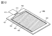
- FIG. 12 is a diagram illustrating a configuration example of a display device.
- FIG. 13A and 13B are diagrams illustrating configuration examples of a display device.
- 14A and 14B are diagrams showing configuration examples of a display device.
- FIG. 15 is a diagram illustrating a configuration example of a display device.
- FIG. 16 is a diagram illustrating a configuration example of a display device.
- FIG. 17 is a diagram illustrating a configuration example of a display device.
- FIG. 18 is a diagram illustrating a configuration example of a display device.
- FIG. 19 is a diagram illustrating a configuration example of a display device.
- FIG. 20 is a diagram illustrating a configuration example of a display device.
- 21A to 21F are diagrams showing configuration examples of light-emitting devices.
- 22A and 22B are diagrams showing configuration examples of light receiving devices.
- 22C to 22E are diagrams showing configuration examples of display devices.
- 23A to 23D are diagrams illustrating configuration examples of electronic devices.
- 24A to 24F are diagrams illustrating configuration examples of electronic devices.
- 25A to 25G are diagrams illustrating configuration examples of electronic devices.
- 26A and 26B are MTF measurement results.
- FIG. 1 shows a configuration example of the display device 10.
- the display device 10 has a display panel 20 and a signal generator 30 .
- the signal generator 30 has a function of generating a signal for displaying a predetermined image based on data received from the outside and outputting the signal to the display panel 20 .
- the display panel 20 has a function of displaying an image on the display section according to the signal input from the signal generation section 30 .
- the display panel 20 has a pixel portion 21 configured by a plurality of pixels 22, a driving circuit 23, and a driving circuit 24.
- FIG. 1 A pixel portion 21 configured by a plurality of pixels 22, a driving circuit 23, and a driving circuit 24.
- the pixels 22 each have a display element and have a function of displaying a predetermined gradation.
- the gradation of the pixels 22 is controlled by the signals output from the driving circuits 23 and 24 , and a predetermined image is displayed on the pixel portion 21 .
- Examples of display elements provided in the pixels 22 include liquid crystal elements and light emitting elements.
- a transmissive liquid crystal element, a reflective liquid crystal element, a transflective liquid crystal element, or the like can be used.
- a shutter type MEMS (Micro Electro Mechanical Systems) element, an optical interference type MEMS element, a microcapsule type, an electrophoresis type, an electrowetting type, an electronic liquid powder (registered trademark) type, etc. are applied.
- a display element or the like can also be used.
- light-emitting elements include self-luminous light-emitting elements such as OLEDs (Organic Light Emitting Diodes), LEDs (Light Emitting Diodes), QLEDs (Quantum-dot Light Emitting Diodes), and semiconductor lasers.
- OLEDs Organic Light Emitting Diodes
- LEDs Light Emitting Diodes
- QLEDs Quadantum-dot Light Emitting Diodes
- semiconductor lasers examples include self-luminous light-emitting elements such as OLEDs (Organic Light Emitting Diodes), LEDs (Light Emitting Diodes), QLEDs (Quantum-dot Light Emitting Diodes), and semiconductor lasers.
- M ⁇ N pixels 22 are provided in the pixel unit 21 .
- the number of pixels 22 provided in the pixel portion 21 can be freely set. For example, when displaying 4K2K video on the display panel 20, it is preferable to provide 3840 ⁇ 2160 or more pixels 22 or 4096 ⁇ 2160 or more pixels 22 in the pixel portion 21 . Further, when displaying 8K4K video, it is preferable to provide 7680 ⁇ 4320 or more pixels 22 in the pixel portion 21 . Also, more pixels 22 can be provided in the pixel portion 21 .
- the pixels 22 are connected to the wiring SL and the wiring GL, respectively. Further, the wirings GL are connected to the driving circuit 23 respectively, and the wirings SL are connected to the driving circuit 24 respectively.
- the drive circuit 23 has a function of supplying a signal for selecting the pixel 22 (hereinafter also referred to as a selection signal) to the pixel 22 .
- the driver circuit 23 has a function of supplying a selection signal to the wiring GL
- the wiring GL has a function of transmitting the selection signal output from the driver circuit 23 to the pixel 22 .
- the driving circuit 23 can be called a scanning line driving circuit, a gate driving circuit, a gate driver, or the like.
- the wiring GL can also be called a selection signal line, a gate line, or the like.
- the drive circuit 24 has a function of supplying video signals to the pixels 22 .
- the driver circuit 24 has a function of supplying a video signal to the wiring SL
- the wiring SL has a function of transmitting the video signal output from the driver circuit 24 to the pixel 22 .
- the driver circuit 24 can be called a signal line driver circuit, a source driver circuit, a source driver, or the like.
- the wiring SL can also be called a video signal line, a source line, or the like.
- a video signal is supplied to the pixel 22 to which the selection signal is supplied, so that the video signal is written in the pixel 22 and a predetermined gradation is displayed.
- the signal generator 30 has a function of generating a video signal based on data input from the outside.
- the signal generation section 30 includes a front end section FE, a decoder DEC, a processing circuit PC, a correction circuit CC, a reception section RCV, an interface IF, a storage section MEM, a control circuit CTRL, and the like.
- the front end unit FE has a function of receiving signals input from the outside and appropriately performing signal processing.
- the front-end unit FE receives, for example, a broadcast signal that has been coded and modulated by a predetermined method.
- the front-end unit FE can have a function of demodulating received video signals, analog-to-digital conversion, and the like.
- the front end section FE may have a function of performing error correction. Data received by the front-end unit FE and subjected to signal processing are output to the decoder DEC.
- the decoder DEC has the function of decoding the encoded signal.
- the decoder DEC may comprise functionality to perform inverse quantization, inverse orthogonal transforms such as inverse discrete cosine transform (IDCT) or inverse discrete sine transform (IDST), entropy decoding, intra-frame prediction, inter-frame prediction, etc. can.
- IDCT inverse discrete cosine transform
- IDST inverse discrete sine transform
- HEVC High Efficiency Video Coding
- Decoding processing by the decoder DEC generates image data SD and outputs it to the processing circuit PC.
- FIG. 1 shows an example in which a signal is input to the front end section FE via an antenna, it is not limited to this.
- the front end unit FE may function as an interface that receives various image signals as well as broadcast signals.
- the front-end part FE can also receive a digital image signal generated by an arithmetic processing unit such as a CPU (Central Processing Unit) or a GPU (Graphics Processing Unit). At this time, the image signal may be output to the processing circuit PC without going through the decoder DEC.
- an arithmetic processing unit such as a CPU (Central Processing Unit) or a GPU (Graphics Processing Unit).
- the front-end unit FE can also receive data TD, which is video data used when performing correction processing, from the correction system 40 .
- the processing circuit PC has a function of performing image processing on the image data SD input from the decoder DEC to generate data SD1 and outputting it to the correction circuit CC.
- image processing examples include noise removal processing, gradation conversion processing, color tone correction processing, and brightness correction processing.
- Color tone correction processing and luminance correction processing can be performed using gamma correction or the like.
- the processing circuit PC may have a function of executing inter-pixel interpolation processing associated with resolution up-conversion, inter-frame interpolation processing associated with frame frequency up-conversion, and the like.
- Noise reduction processing includes the removal of various types of noise, such as mosquito noise that occurs around the contours of characters, block noise that occurs in high-speed moving images, random noise that causes flickering, and dot noise that occurs when resolution is upconverted. .
- the gradation conversion process is a process of converting the gradation indicated by the data SD1 into a gradation corresponding to the output characteristics of the display panel 20. For example, when the number of gradations is increased, processing for smoothing the histogram can be performed by interpolating and assigning gradation values corresponding to each pixel to image data input with a small number of gradations. . Moreover, high dynamic range (HDR) processing for widening the dynamic range is also included in the gradation conversion processing.
- HDR high dynamic range
- Color tone correction processing is processing for correcting the color tone of the video.
- the brightness correction process is a process of correcting the brightness (brightness contrast) of the image.
- the brightness and color tone of the image displayed on the display panel 20 are corrected to be optimal according to the type, brightness, color purity, etc. of lighting installed in the space where the display panel 20 is provided.
- Inter-pixel interpolation processing is processing that interpolates data that originally does not exist when the resolution is up-converted. For example, as color data of a pixel to be newly interpolated (e.g., gradation values corresponding to red (R), green (G), and blue (B)), color data of pixels surrounding the pixel in question is referenced. Then, the data is interpolated so that it becomes the data of the intermediate color.
- color data of a pixel to be newly interpolated e.g., gradation values corresponding to red (R), green (G), and blue (B)
- RGB red
- G green
- B blue
- Inter-frame interpolation processing is processing that generates an image of a frame (interpolation frame) that originally does not exist when increasing the frame frequency of the video to be displayed.
- an interpolation frame image to be inserted between two images is generated from the difference between two images.
- a plurality of interpolated frame images can be generated between two images.
- the frame frequency of the image data is 60 Hz
- the frame frequency of the video signal output to the display panel 20 is doubled to 120 Hz, or quadrupled to 240 Hz, or It can be increased by eight times to 480 Hz, and so on.
- the above image processing can also be performed by an image processing circuit provided separately from the processing circuit PC.
- the correction circuit CC has a function of correcting the data SD1 input from the processing circuit PC based on the correction data W and generating corrected data SD2.
- Data SD2 corrected by the correction circuit CC is output to the drive circuit 24 of the display panel 20.
- FIG. The display panel 20 can display an image on the pixel portion 21 based on the data SD2.
- the receiving unit RCV has a function of receiving externally input data or control signals.
- Examples of the receiving unit RCV include an external connection terminal such as a data input terminal or video input terminal, or a wireless communication module.
- the correction data W and the like used in the correction circuit CC are transmitted from the correction system 40 and the like provided outside the signal generation section 30, and can be received by the reception section RCV.
- the interface IF has a function of appropriately performing signal processing on the data or control signal received by the receiving unit RCV and outputting it to the storage unit MEM or the control circuit CTRL.
- the control circuit CTRL has a function of controlling the operation of each circuit included in the signal generation section 30 .
- the control circuit CTRL has a function of supplying control signals to the decoder DEC, the processing circuit PC, the correction circuit CC, the memory unit MEM, and the like. Control by the control circuit CTRL may be performed based on a control signal or the like received by the receiver RCV.
- the storage unit MEM has a function of storing data. Correction data W is stored in the storage unit MEM.
- the memory unit MEM preferably has a non-volatile memory device so that the correction data W can be retained even when the power supply to the display device 10 is stopped.
- the correction circuit CC Under the control of the control circuit CTRL, the correction circuit CC reads the correction data W from the storage unit MEM, corrects the data SD1 using the correction data W, and generates data SD2.
- the correction data W may be read only when the display device 10 is started.
- the correction circuit CC is configured to have a memory in addition to the processor.
- the display device 10 can constitute part of an electronic device that includes a display unit.
- a display unit For example, ultra-large equipment such as for digital signage, large equipment such as television equipment or monitor equipment, medium-sized equipment such as tablet terminals or notebook terminals, small equipment such as smartphones or wristwatch terminals, and VR
- the display device 10 can be applied to electronic devices having display portions of various sizes, such as ultra-compact devices for AR.
- the correction system exemplified below has a function of generating correction data W to be supplied to the display device 10 exemplified above.
- the display device 10 can display an image based on the data SD2 corrected using the correction data W supplied from the correction system.
- the correction system has a function of determining whether the display quality of the corrected display of the display device 10 is acceptable or unacceptable. If the display quality does not exceed the specified level despite the correction, the display device 10 can be determined to be defective.
- FIG. 2 shows a configuration example of the correction system 40. As shown in FIG. In FIG. 2, the correction system 40 and the display device 10 are shown. For simplicity, FIG. 2 shows only part of the display panel 20 and part of the signal generator 30 as the display device 10 , but FIG. 1 can be referred to for the configuration of the display device 10 .
- the correction system 40 has a processing device 45 and an imaging device 44 .
- the correction system 40 outputs data TD to the display device 10 and causes the display panel 20 to display an image based on the data TD.
- Data W can be generated.
- the imaging device 44 can image all the pixels 22 included in the pixel section 21 of the display panel 20 .
- the captured image data is output to the processing device 45 as image data VD.
- the imaging device 44 for example, a camera or a two-dimensional luminance meter can be used.
- the processing device 45 has a correction data generation unit 41, a signal generation unit 42, a timing controller 43, and a determination unit 46.
- the signal generator 42 has a function of generating data TD.
- the signal generator 42 can generate data TD, which is image data to be output to the display device 10, based on test patterns stored in advance. Thereby, the test pattern can be displayed on the pixel portion 21 of the display device 10 .
- the timing controller 43 has a function of adjusting the timing of displaying the test pattern on the display device 10 and the timing of imaging by the imaging device 44 .
- the timing controller 43 has a function of generating the data CD, which is a control signal for controlling the imaging timing of the imaging device 44 .
- the timing controller 43 also outputs the data TD to the display device 10 and the data CD to the imaging device 44 so that they are synchronized with each other.
- the correction data generation unit 41 has a function of generating correction data W based on the imaging data VD and outputting it to the display device 10 .
- the judging unit 46 has a function of judging whether the display quality is acceptable or unacceptable based on the imaging data VD. Unlike the imaging data VD for correction, the imaging data VD used for determination need not include information of all pixels, and the imaging data VD can be optimized according to the determination method.
- the image capturing device 44 captures images of all pixels of the display panel 20 . Therefore, the imaging method can be varied according to the size of the display panel 20 or the resolution, focal length, angle of view, etc. of the imaging device 44 .
- FIG. 3A shows an example of an imaging method when the size of the pixel section 21 of the display device 10 is larger than the imaging range 48 of the imaging device 44 .
- FIG. 3A by scanning the imaging device 44 or the display device 10 to capture an image, luminance information of all pixels can be obtained.
- FIG. 3B shows an example of an imaging method when the size of the pixel section 21 of the display device 10 is within the imaging range 48 of the imaging device 44 .
- luminance information of all pixels can be acquired by one-time imaging.
- the resolution (the number of pixels) of the imaging device 44 larger than the resolution (the number of pixels) of the pixel section 21 of the display panel 20, the brightness of all the pixels of the display panel 20 can be obtained with high accuracy.
- FIG. 3C shows an example of an imaging method when imaging a plurality of display devices 10 at the same time.
- the display device 10 is moved by the carrier device 51 .
- a plurality of fixed imaging devices 44 are arranged above the conveying device 51 .
- the display device 10 is transported by the transport device 51 so as to pass through the imaging range 48 of one of the imaging devices 44 . This makes it possible to perform correction processing for a plurality of display devices 10 at the same time, which is suitable for mass production of display devices 10 .
- the brightness of each pixel is acquired while all pixels are displayed with a predetermined gradation value. At this time, it is preferable to display the image without performing the correction because more effective correction data can be generated.
- FIG. 4A is a diagram schematically showing luminance data L(40) when the gradation value is 40.
- the luminance data L(40) includes luminance value information corresponding to all the pixels 22 provided in the pixel portion 21 of the display panel 20.
- FIG. FIG. 4A shows luminance values corresponding to 4 ⁇ 4 pixels including pixels in i rows and j columns (where i is an integer of 1 to M and j is an integer of 1 to N). The luminance value of each pixel is shown when the predetermined luminance when displaying with a gradation value of 40 is 40.
- the luminance value of the i-th row and j-th column pixel is expressed as L i,j (40).
- a pixel with a luminance value exceeding 40 means that the pixel is lit brighter than predetermined, and a pixel with a luminance value of less than 40 means that it is lit darker than predetermined.
- FIG. 4B shows difference data D(40) indicating a difference value between each luminance value of luminance data L(40) and a predetermined luminance value of 40.
- the difference value of the i-th row and j-th pixel is expressed as D i,j (40).
- a pixel with a positive difference value is brighter than a predetermined value, and a pixel with a negative difference value is darker than a predetermined value.
- the difference data D shown here is for the sake of explanation, and the difference data D does not necessarily have to be calculated when the correction data W is generated.
- the difference data D(40) illustrated in FIG. 4B indicates the difference from the predetermined brightness
- the image data input to the display panel 20 is corrected in advance so as to cancel the difference
- the correction value of the pixel in the i-th row and j-th column of the correction data W(40) is expressed as W i,j (40).
- the correction data W(40) when the gradation value T is 40 is taken as an example, but for a plurality of gradation values T, the correction data W(T) can be generated in a similar manner.
- the correction data W is a data table from correction data W(0) when the gradation value T is 0 to correction data W(255) when the gradation value T is 255. can do.
- Each correction data W(T) contains M ⁇ N data from the correction value W 1,1 (T) of the pixel in the first row and the first column to the correction value W M,N (T) of the pixel in the M row and N column. correction values are included.
- the correction data W may be generated by generating (T) and interpolating the correction data W(T) therebetween.
- an interpolation method such as linear interpolation or nonlinear interpolation can be used as appropriate.
- a full-color display panel actually has three sub-pixels of red (R), green (G), and blue (B). Therefore, it is preferable to generate correction data W for each color. Also, in the case where there are yellow (Y) or white (W) sub-pixels in addition to R, G, and B, correction data W can be similarly generated for these colors.
- FIG. 5A shows an example of luminance data L(40) when the pixel in the i+1-th row and the j+2-th column is a dark spot defect. Since the pixel is not lit, the luminance value L i+1,j+2 (40) is 0.
- the correction data generation unit 41 can determine that a pixel having a luminance value of 0 or its vicinity is a point defect pixel.
- the difference value D i+1,j+2 (40) of the pixel is represented by X to indicate that it is the data of the dark spot defect pixel.
- the correction values for each of the eight pixels surrounding the dark spot defect pixel are set higher than the original correction values.
- the tone value T is 40
- the correction values are modified so that the luminance value is 47 for the four pixels positioned above, below, to the left, and to the right of the pixel with the dark spot defect, and the nearest pixel positioned diagonally with respect to the pixel with the dark spot defect. This is an example in which the correction values are corrected so that the luminance value becomes 43 for four pixels.
- the corrected value of the correction value for the pixels surrounding the pixel with the dark spot defect is appropriately determined according to the configuration of the display panel 20. can be set. Also, here, the method of compensating the luminance using eight pixels surrounding the pixel with the dark spot defect has been described, but the present invention is not limited to this, and the luminance is compensated using seven or less or nine or more pixels. You may Also in this case, it is preferable to set a higher correction value as the pixel is closer to the dark spot defect.
- a mark (here, X) indicating a dark spot defect pixel can be left in the correction data W(40). That is, it can be said that the correction data W(40) has the address information of the dark spot defect pixel.
- the correction data W(40) has the address information of the dark spot defect pixel.
- the correction value should be set so that the luminance value of the pixels surrounding the bright spot defect is lowered.
- FIG. 6 is a flowchart for the correction processing described below.
- the flowchart shown in FIG. 6 has steps S01 to S08.
- images are repeatedly captured A times (A is an integer equal to or greater than 1 and equal to or less than the maximum number of gradations of the display device 10) at different gradations, and correction data W is generated based on each imaged data. This is an example of generating.
- step S01 the correction process is started.
- step 03 all pixels of the display panel 20 are displayed in the n-th gradation, and an image is captured using the imaging method described above to obtain the n-th imaged data.
- the signal generator 42 generates data TD, which is image data of a predetermined gradation, and the timing controller 43 outputs the data TD to the display device 10 and the data CD to the imaging device 44, respectively. Since the imaging device 44 captures images of all pixels, the imaging device 44 performs multiple times of imaging as necessary, and outputs the imaging data VD to the correction data generation unit 41 .
- step S04 if n is less than A (no), proceed to step S05.
- correction data W is generated based on the acquired first to n-th imaging data (that is, first to A-th data).
- the above description can be referred to.
- step S07 the generated correction data W is output to the display device 10.
- the display device 10 stores the correction data W in the storage unit MEM via the reception unit RCV and the interface IF.
- FIG. 7 shows a flowchart of the correction method in that case.
- the determination processing illustrated below is performed by, for example, the determination unit 46 illustrated in FIG. 2, the imaging device 44, and the like.
- the determination process causes the display device 10 to display an image corrected based on the correction data W, and determines whether the display quality satisfies a predetermined standard.
- this correction method is used for pre-shipment inspection of products, it is possible to prevent products whose display quality does not meet the standards even after correction with the correction data W from entering the market.
- MTF modulation transfer function
- LSF line spread function
- Fig. 8 shows an example of MTF measurement results.
- Three MTF curves of display panel A, display panel B, and display panel C are shown in descending order of display quality.
- the vertical axis indicates the MTF value (%).
- the horizontal axis indicates the spatial frequency in cpp (cycles per pixel). Spatial frequencies range from greater than 0 to less than 0.5.
- a state in which the spatial frequency is 0.5 indicates, for example, a state in which white and black lines are displayed at a pitch of 1 pixel, and is equivalent to a state in which the finest pattern is displayed.
- a determination method for example, it is determined whether or not the MTF value when the spatial frequency is 0.5 exceeds a predetermined threshold value (Vth).
- Vth a predetermined threshold value
- the display panel A and the display panel B can be determined as non-defective products because the MTF value exceeds the threshold when the spatial frequency is 0.5.
- the MTF value of the display panel C since the MTF value of the display panel C has not reached the threshold value, it can be determined as a defective product.
- the flowchart shown in FIG. 9 has steps S11 to S18.
- step S11 the process is started.
- step S12 the display panel 20 is caused to display an MTF image, which is a test image, and the imaging device 44 acquires MTF imaging data.
- the MTF image (test image) an image of a white line with a width of 1 pixel or various chart images can be used.
- images of various patterns can be used as long as the MTF can be calculated.
- the MTF image measurement may be performed using not only a still image but also a moving image.
- the MTF value By measuring the MTF value using a moving image, for example, the degree of afterimage can be evaluated.
- step S13 the MTF value is calculated based on the MTF imaging data.
- the MTF values are calculated for each location, and the lowest value among them can be used as the MTF value.
- step S14 it is determined whether or not the MTF value is greater than or equal to the threshold value.
- step S14 If the MTF value is equal to or greater than the threshold value in step S14 (yes), the process proceeds to step S16, and the display device 10 is determined to be acceptable (non-defective product). After that, the process ends in step S18.
- step S14 If the MTF value is less than the threshold value in step S14 (no), the process proceeds to step S15, and the display device 10 is determined to be rejected (defective product). After that, the process ends in step S17.
- correction values for all grayscales can be set for all pixels included in the display device. Even if luminance unevenness occurs, the display quality can be greatly improved. In addition, by performing the determination process using the MTF after the correction process, it is possible to effectively prevent products that are determined to be defective even after the correction from entering the market by a simple method.
- This embodiment can be implemented by appropriately combining at least part of it with other embodiments described herein.
- Embodiment 2 In this embodiment, a configuration example of a display device to which the correction method or the correction system of one embodiment of the present invention can be applied will be described.
- the display device exemplified below can be applied to the display panel 20 and the like of the first embodiment.
- One embodiment of the present invention is a display device including a light-emitting element (also referred to as a light-emitting device).
- a display device has two or more light-emitting elements that emit light of different colors. Each light-emitting element has a pair of electrodes and an EL layer therebetween.
- the light-emitting element is preferably an organic EL element (organic electroluminescence element). Two or more light-emitting elements with different emission colors have EL layers containing different light-emitting materials.
- a full-color display device can be realized by using three types of light-emitting elements that emit red (R), green (G), and blue (B) light.
- the layer profile may be blurred and the edge thickness may be reduced.
- the thickness of the island-shaped light-emitting layer may vary depending on the location.
- countermeasures have been taken to artificially increase the definition (also called pixel density) by adopting a special pixel arrangement method such as a pentile arrangement.
- an island shape indicates a state in which two or more layers using the same material formed in the same process are physically separated.
- an island-shaped light-emitting layer means that the light-emitting layer is physically separated from an adjacent light-emitting layer.
- an EL layer is processed into a fine pattern by photolithography without using a shadow mask such as a fine metal mask (FMM).
- a shadow mask such as a fine metal mask (FMM).
- FMM fine metal mask
- the EL layers can be separately formed, a display device with extremely vivid, high contrast, and high display quality can be realized.
- the EL layer may be processed into a fine pattern using both a metal mask and photolithography.
- part or all of the EL layer can be physically separated. Accordingly, leakage current between light-emitting elements can be suppressed through a layer (also referred to as a common layer) used in common between adjacent light-emitting elements. Thereby, crosstalk due to unintended light emission can be prevented, and a display device with extremely high contrast can be realized. In particular, a display device with high current efficiency at low luminance can be realized.
- One embodiment of the present invention can also be a display device in which a light-emitting element that emits white light and a color filter are combined.
- light-emitting elements having the same structure can be applied to light-emitting elements provided in pixels (sub-pixels) that emit light of different colors, and all layers can be common layers. Further, part or all of each EL layer is divided by photolithography. As a result, leakage current through the common layer is suppressed, and a high-contrast display device can be realized.
- a device having a tandem structure in which a plurality of light-emitting layers are stacked via a highly conductive intermediate layer, it is possible to effectively prevent leakage current through the intermediate layer, resulting in high brightness and high definition. , and high contrast.
- an insulating layer covering at least the side surface of the island-shaped light emitting layer.
- the insulating layer may cover part of the top surface of the island-shaped EL layer.
- a material having barrier properties against water and oxygen is preferably used for the insulating layer.
- an inorganic insulating film that hardly diffuses water or oxygen can be used. Accordingly, deterioration of the EL layer can be suppressed, and a highly reliable display device can be realized.
- a phenomenon occurs in which the common electrode is divided by a step at the end of the EL layer (also referred to as step disconnection). may insulate. Therefore, it is preferable to adopt a structure in which a local step located between two adjacent light emitting elements is filled with a resin layer functioning as a planarization film (also called LFP: Local Filling Planarization).
- the resin layer has a function as a planarizing film.
- FIG. 10A shows a schematic top view of a display device 100 of one embodiment of the present invention.
- the display device 100 includes, on a substrate 101, a plurality of red light emitting elements 110R, green light emitting elements 110G, and blue light emitting elements 110B.
- the light emitting region of each light emitting element is labeled with R, G, and B.
- FIG. 10A in order to easily distinguish each light emitting element, the light emitting region of each light emitting element is labeled with R, G, and B.
- the light emitting elements 110R, 110G, and 110B are arranged in a matrix.
- FIG. 10A shows a so-called stripe arrangement in which light emitting elements of the same color are arranged in one direction.
- the arrangement method of the light emitting elements is not limited to this, and an arrangement method such as an S-stripe arrangement, a delta arrangement, a Bayer arrangement, or a zigzag arrangement may be applied, or a pentile arrangement, a diamond arrangement, or the like may be used.
- the light emitting element 110R, the light emitting element 110G, and the light emitting element 110B for example, an OLED (Organic Light Emitting Diode) or a QLED (Quantum-dot Light Emitting Diode) is preferably used.
- the light-emitting substance of the EL element include a substance that emits fluorescence (fluorescent material), a substance that emits phosphorescence (phosphorescence material), and a substance that exhibits thermally activated delayed fluorescence (thermally activated delayed fluorescence: TADF ) materials).
- a light-emitting substance included in an EL element not only an organic compound but also an inorganic compound (such as a quantum dot material) can be used.
- FIG. 10A also shows a connection electrode 111C electrically connected to the common electrode 113.
- FIG. 111 C of connection electrodes are given the electric potential (for example, anode electric potential or cathode electric potential) for supplying to the common electrode 113.
- FIG. The connection electrode 111C is provided outside the display area where the light emitting elements 110R and the like are arranged.
- connection electrodes 111C can be provided along the periphery of the display area. For example, it may be provided along one side of the periphery of the display area, or may be provided over two or more sides of the periphery of the display area. That is, when the top surface shape of the display area is rectangular, the top surface shape of the connection electrode 111C can be strip-shaped (rectangular), L-shaped, U-shaped (square bracket-shaped), square, or the like. .
- FIGS. 10B and 10C are schematic cross-sectional views corresponding to dashed-dotted lines A1-A2 and dashed-dotted lines A3-A4 in FIG. 10A, respectively.
- FIG. 10B shows a schematic cross-sectional view of the light-emitting elements 110R, 110G, and 110B
- FIG. 10C shows a schematic cross-sectional view of the connection portion 140 where the connection electrode 111C and the common electrode 113 are connected. ing.
- the light emitting element 110R has a pixel electrode 111R, an organic layer 112R, a common layer 114, and a common electrode 113.
- the light emitting element 110G has a pixel electrode 111G, an organic layer 112G, a common layer 114, and a common electrode 113.
- the light emitting element 110B has a pixel electrode 111B, an organic layer 112B, a common layer 114, and a common electrode 113.
- the common layer 114 and the common electrode 113 are commonly provided for the light emitting elements 110R, 110G, and 110B.
- the organic layer 112R of the light-emitting element 110R has at least a light-emitting organic compound that emits red light.
- the organic layer 112G included in the light-emitting element 110G contains at least a light-emitting organic compound that emits green light.
- the organic layer 112B included in the light-emitting element 110B contains at least a light-emitting organic compound that emits blue light.
- Each of the organic layer 112R, the organic layer 112G, and the organic layer 112B can also be called an EL layer and has at least a layer containing a light-emitting organic compound (light-emitting layer).
- the light-emitting element 110R, the light-emitting element 110G, and the light-emitting element 110B may be referred to as the light-emitting element 110 when describing matters common to them.
- the symbols omitting the letters may be used. be.
- the organic layer 112 and the common layer 114 may each independently have one or more of an electron injection layer, an electron transport layer, a hole injection layer, and a hole transport layer.
- the organic layer 112 may have a layered structure of a hole injection layer, a hole transport layer, a light emitting layer, and an electron transport layer from the pixel electrode 111 side, and the common layer 114 may have an electron injection layer. .
- a pixel electrode 111R, a pixel electrode 111G, and a pixel electrode 111B are provided for each light emitting element.
- the common electrode 113 and the common layer 114 are provided as a continuous layer common to each light emitting element.
- a conductive film having a property of transmitting visible light is used for one of the pixel electrodes and the common electrode 113, and a conductive film having a reflective property is used for the other.
- a protective layer 121 is provided on the common electrode 113 to cover the light emitting elements 110R, 110G, and 110B.
- the protective layer 121 has a function of preventing impurities such as water from diffusing into each light emitting element from above.
- the end of the pixel electrode 111 preferably has a tapered shape.
- the portion of the organic layer 112 provided along the side surface of the pixel electrode also has a tapered shape.
- the side surface of the pixel electrode is tapered because foreign matter (eg, dust or particles) in the manufacturing process can be easily removed by a treatment such as cleaning.
- the tapered shape refers to a shape in which at least a part of the side surface of the structure is inclined with respect to the substrate surface.
- the organic layer 112 is processed into an island shape by photolithography. Therefore, the organic layer 112 has a shape in which the angle formed by the top surface and the side surface is close to 90 degrees at the end.
- an organic film formed using FMM (Fine Metal Mask) or the like tends to gradually decrease in thickness closer to the end. Since it is formed in a slope shape, it is difficult to distinguish between the top surface and the side surface.
- An insulating layer 125, a resin layer 126, and a layer 128 are provided between two adjacent light emitting elements.
- the resin layer 126 is positioned between two adjacent light emitting elements and is provided so as to fill the end portions of the respective organic layers 112 and the area between the two organic layers 112 .
- the resin layer 126 has a smooth convex upper surface, and a common layer 114 and a common electrode 113 are provided to cover the upper surface of the resin layer 126 .
- the resin layer 126 functions as a flattening film that fills the steps located between the two adjacent light emitting elements. By providing the resin layer 126, a phenomenon in which the common electrode 113 is divided by a step at the end of the organic layer 112 (also referred to as step disconnection) occurs, and the common electrode on the organic layer 112 is prevented from being insulated. be able to.
- the resin layer 126 can also be called LFP (Local Filling Planarization).
- An insulating layer containing an organic material can be suitably used as the resin layer 126 .
- acrylic resin, polyimide resin, epoxy resin, imide resin, polyamide resin, polyimideamide resin, silicone resin, siloxane resin, benzocyclobutene-based resin, phenolic resin, and precursors of these resins are applied as the resin layer 126. can do.
- an organic material such as polyvinyl alcohol (PVA), polyvinyl butyral, polyvinylpyrrolidone, polyethylene glycol, polyglycerin, pullulan, water-soluble cellulose, or alcohol-soluble polyamide resin may be used.
- a photosensitive resin can be used as the resin layer 126 .
- a photoresist may be used as the photosensitive resin.
- a positive material or a negative material can be used for the photosensitive resin.
- the resin layer 126 may contain a material that absorbs visible light.
- the resin layer 126 itself may be made of a material that absorbs visible light, or the resin layer 126 may contain a pigment that absorbs visible light.
- a resin that transmits red, blue, or green light and can be used as a color filter that absorbs other light, or a resin that contains carbon black as a pigment and functions as a black matrix, or the like. can be used.
- the insulating layer 125 is provided in contact with the side surface of the organic layer 112 . Also, the insulating layer 125 is provided to cover the upper end portion of the organic layer 112 . A part of the insulating layer 125 is provided in contact with the upper surface of the substrate 101 .
- the insulating layer 125 is located between the resin layer 126 and the organic layer 112 and functions as a protective film to prevent the resin layer 126 from contacting the organic layer 112 .
- the organic layer 112 may be dissolved by an organic solvent or the like used when forming the resin layer 126 . Therefore, by providing the insulating layer 125 between the organic layer 112 and the resin layer 126 as shown in this embodiment mode, the side surface of the organic layer 112 can be protected.
- the insulating layer 125 can be an insulating layer containing an inorganic material.
- an inorganic insulating film such as an oxide insulating film, a nitride insulating film, an oxynitride insulating film, or a nitride oxide insulating film can be used, for example.
- the insulating layer 125 may have a single-layer structure or a laminated structure.
- the oxide insulating film includes a silicon oxide film, an aluminum oxide film, a magnesium oxide film, an indium gallium zinc oxide film, a gallium oxide film, a germanium oxide film, an yttrium oxide film, a zirconium oxide film, a lanthanum oxide film, a neodymium oxide film, and an oxide film.
- Examples include a hafnium film and a tantalum oxide film.
- Examples of the nitride insulating film include a silicon nitride film and an aluminum nitride film.
- As the oxynitride insulating film a silicon oxynitride film, an aluminum oxynitride film, or the like can be given.
- nitride oxide insulating film a silicon nitride oxide film, an aluminum nitride oxide film, or the like can be given.
- a metal oxide film such as a hafnium oxide film, or an inorganic insulating film such as a silicon oxide film to the insulating layer 125, pinholes are reduced and the EL layer can be protected.
- a superior insulating layer 125 can be formed.
- oxynitride refers to a material whose composition contains more oxygen than nitrogen
- nitride oxide refers to a material whose composition contains more nitrogen than oxygen. point to the material.
- silicon oxynitride refers to a material whose composition contains more oxygen than nitrogen
- silicon nitride oxide refers to a material whose composition contains more nitrogen than oxygen. indicates
- a sputtering method, a CVD method, a PLD method, an ALD method, or the like can be used to form the insulating layer 125 .
- the insulating layer 125 is preferably formed by an ALD method with good coverage.
- a reflective film for example, a metal film containing one or more selected from silver, palladium, copper, titanium, and aluminum
- a reflective film is provided between the insulating layer 125 and the resin layer 126 so that A configuration may be adopted in which emitted light is reflected by the reflecting film.
- the light extraction efficiency can be improved.
- the layer 128 is part of a protective layer (also referred to as a mask layer or a sacrificial layer) for protecting the organic layer 112 when the organic layer 112 is etched.
- a protective layer also referred to as a mask layer or a sacrificial layer
- any of the materials that can be used for the insulating layer 125 can be used.
- an aluminum oxide film, a metal oxide film such as a hafnium oxide film, or an inorganic insulating film such as a silicon oxide film formed by an ALD method has few pinholes. It can be suitably used for
- a protective layer 121 is provided to cover the common electrode 113 .
- the protective layer 121 can have, for example, a single layer structure or a laminated structure including at least an inorganic insulating film.
- the inorganic insulating film include oxide films such as a silicon oxide film, a silicon oxynitride film, a silicon nitride oxide film, a silicon nitride film, an aluminum oxide film, an aluminum oxynitride film, and a hafnium oxide film; An oxide film or a nitride film can be used.
- a semiconductor material or a conductive material such as indium gallium oxide, indium zinc oxide, indium tin oxide, or indium gallium zinc oxide may be used for the protective layer 121 .
- a laminated film of an inorganic insulating film and an organic insulating film can also be used as the protective layer 121 .
- a structure in which an organic insulating film is sandwiched between a pair of inorganic insulating films is preferable.
- the organic insulating film functions as a planarizing film.
- the upper surface of the organic insulating film can be flattened, so that the coverage of the inorganic insulating film thereon can be improved, and the barrier property can be enhanced.
- the upper surface of the protective layer 121 is flat, when a structure (for example, a color filter, an electrode of a touch sensor, or a lens array) is provided above the protective layer 121, an uneven shape due to the structure below may be formed. This is preferable because it can reduce the impact.
- a structure for example, a color filter, an electrode of a touch sensor, or a lens array
- FIG. 10C shows a connection portion 140 where the connection electrode 111C and the common electrode 113 are electrically connected.
- the connecting portion 140 an opening is provided in the insulating layer 125 and the resin layer 126 above the connecting electrode 111C.
- the connection electrode 111C and the common electrode 113 are electrically connected through the opening.
- FIG. 10C shows the connection portion 140 where the connection electrode 111C and the common electrode 113 are electrically connected. good.
- the common layer 114 is located at the connection portion 140 because the electrical resistivity of the material used for the common layer 114 is sufficiently low and the thickness can be made thin. Often times there are no problems. As a result, the common electrode 113 and the common layer 114 can be formed using the same shielding mask, so the manufacturing cost can be reduced.
- FIG. 10A A pixel layout different from that in FIG. 10A will be mainly described below.
- the arrangement of the light emitting elements (sub-pixels) is not particularly limited, and various methods can be applied.
- top surface shapes of sub-pixels include triangles, quadrilaterals (including rectangles and squares), polygons such as pentagons, shapes with rounded corners of these polygons, ellipses, and circles.
- the top surface shape of the sub-pixel corresponds to the top surface shape of the light emitting region of the light emitting element.
- a pixel 150 shown in FIG. 11A is composed of three sub-pixels of light emitting elements 110a, 110b, and 110c.
- the light emitting element 110a may be a blue light emitting element
- the light emitting element 110b may be a red light emitting element
- the light emitting element 110c may be a green light emitting element.
- the pixel 150 shown in FIG. 11B includes a light emitting element 110a having a substantially trapezoidal top surface shape with rounded corners, a light emitting element 110b having a substantially triangular top surface shape with rounded corners, and a substantially square or substantially hexagonal top surface shape with rounded corners. and a light emitting element 110c having Further, the light emitting element 110a has a larger light emitting area than the light emitting element 110b. Thus, the shape and size of each light emitting element can be determined independently. For example, a more reliable light-emitting element can be made smaller.
- the light emitting element 110a may be a green light emitting element
- the light emitting element 110b may be a red light emitting element
- the light emitting element 110c may be a blue light emitting element.
- FIG. 11C shows an example in which pixels 124a having light-emitting elements 110a and 110b and pixels 124b having light-emitting elements 110b and 110c are alternately arranged.
- the light emitting element 110a may be a red light emitting element
- the light emitting element 110b may be a green light emitting element
- the light emitting element 110c may be a blue light emitting element.
- the pixel 124a has two light emitting elements (light emitting elements 110a and 110b) in the upper row (first row) and one light emitting element (light emitting element 110c) in the lower row (second row).
- the pixel 124b has one light emitting element (light emitting element 110c) in the upper row (first row) and two light emitting elements (light emitting elements 110a and 110b) in the lower row (second row).
- the light emitting element 110a may be a red light emitting element
- the light emitting element 110b may be a green light emitting element
- the light emitting element 110c may be a blue light emitting element.
- FIG. 11D is an example in which each light emitting element has a substantially square top surface shape with rounded corners
- FIG. 11E is an example in which each light emitting element has a circular top surface shape.
- FIG. 11F is an example in which light emitting elements of each color are arranged in a zigzag pattern. Specifically, when viewed from above, the upper sides of two light emitting elements (for example, light emitting elements 110a and 110b, or light emitting elements 110b and 110c) aligned in the column direction are displaced.
- the light emitting element 110a may be a red light emitting element
- the light emitting element 110b may be a green light emitting element
- the light emitting element 110c may be a blue light emitting element.
- the top surface shape of the light emitting element may be a polygonal shape with rounded corners, an elliptical shape, a circular shape, or the like.
- the EL layer is processed into an island shape using a resist mask.
- the resist film formed on the EL layer needs to be cured at a temperature lower than the heat resistance temperature of the EL layer. Therefore, depending on the heat resistance temperature of the EL layer material and the curing temperature of the resist material, curing of the resist film may be insufficient.
- a resist film that is insufficiently hardened may take a shape away from the desired shape during processing.
- the top surface shape of the EL layer may be a polygon with rounded corners, an ellipse, or a circle. For example, when a resist mask having a square top surface is formed, a resist mask having a circular top surface is formed, and the EL layer may have a circular top surface.
- a technique for correcting the mask pattern in advance so that the design pattern and the transfer pattern match.
- OPC Optical Proximity Correction
- a pattern for correction is added to a corner portion of a figure on a mask pattern.
- This embodiment can be implemented by appropriately combining at least part of it with other embodiments described herein.
- the display device of the present embodiment is, for example, a television device, a desktop or notebook personal computer, a computer monitor, digital signage, a large game machine such as a pachinko machine, or other electronic device having a relatively large screen.
- a television device for example, a desktop or notebook personal computer, a computer monitor, digital signage, a large game machine such as a pachinko machine, or other electronic device having a relatively large screen.
- it can be used for display parts of digital cameras, digital video cameras, digital photo frames, mobile phones, mobile game machines, smart phones, wristwatch terminals, tablet terminals, personal digital assistants, and sound reproducing devices.
- FIG. 12 shows a perspective view of the display device 400
- FIG. 13A shows a cross-sectional view of the display device 400. As shown in FIG.
- the display device 400 has a configuration in which a substrate 452 and a substrate 451 are bonded together.
- the substrate 452 is clearly indicated by dashed lines.
- the display device 400 has a display section 462, a circuit 464, wiring 465, and the like.
- FIG. 12 shows an example in which an IC 473 and an FPC 472 are mounted on the display device 400 . Therefore, the configuration shown in FIG. 12 can also be said to be a display module including the display device 400, an IC (integrated circuit), and an FPC.
- a scanning line driving circuit for example, can be used as the circuit 464 .
- the wiring 465 has a function of supplying signals and power to the display section 462 and the circuit 464 .
- the signal and power are input to the wiring 465 from the outside through the FPC 472 or input to the wiring 465 from the IC 473 .
- FIG. 12 shows an example in which an IC 473 is provided on a substrate 451 by a COG (Chip On Glass) method, a COF (Chip on Film) method, or the like.
- IC 473 for example, an IC having a scanning line driver circuit, a signal line driver circuit, or the like can be applied.
- the display device 400 and the display module may be configured without an IC.
- the IC may be mounted on the FPC by the COF method or the like.
- FIG. 13A shows an example of a cross section of the display device 400 when part of the region including the FPC 472, part of the circuit 464, part of the display portion 462, and part of the region including the connection portion are cut. show.
- FIG. 13A shows an example of a cross section of the display portion 462, in particular, a region including the light emitting element 430b that emits green light and the light emitting element 430c that emits blue light.
- the display device 400 illustrated in FIG. 13A includes the transistor 202, the transistor 210, the light-emitting elements 430b, 430c, and the like between the substrate 453 and the substrate 454.
- the light-emitting elements exemplified in Embodiment 2 can be applied to the light-emitting elements 430b and 430c.
- the three sub-pixels are red (R), green (G), and blue (B).
- Color sub-pixels such as yellow (Y), cyan (C), and magenta (M) sub-pixels.
- the four sub-pixels include R, G, B, and white (W) sub-pixels, and R, G, B, and Y four-color sub-pixels. be done.
- the substrate 454 and the protective layer 416 are adhered via the adhesive layer 442 .
- the adhesive layer 442 is provided so as to overlap each of the light emitting elements 430b and 430c, and the display device 400 has a solid sealing structure.
- the light-emitting elements 430b and 430c have conductive layers 411a, 411b, and 411c as pixel electrodes.
- the conductive layer 411b reflects visible light and functions as a reflective electrode.
- the conductive layer 411c is transparent to visible light and functions as an optical adjustment layer.
- the conductive layer 411 a is connected to the conductive layer 222 b included in the transistor 210 through an opening provided in the insulating layer 214 .
- the transistor 210 has a function of controlling driving of the light emitting element.
- An EL layer 412G or an EL layer 412B is provided to cover the pixel electrodes.
- An insulating layer 421 is provided in contact with a side surface of the EL layer 412G and a side surface of the EL layer 412B, and a resin layer 422 is provided so as to fill recesses of the insulating layer 421.
- FIG. A layer 424 is provided between the EL layer 412G and the insulating layer 421 and between the EL layer 412B and the insulating layer 421, respectively.
- a common layer 414, a common electrode 413, and a protective layer 416 are provided to cover the EL layers 412G and 412B.
- the light emitted by the light emitting element is emitted to the substrate 454 side.
- a material having high visible light transmittance is preferably used for the substrate 454 .
- Both the transistor 202 and the transistor 210 are formed over the substrate 453 . These transistors can be made with the same material and the same process.
- the substrate 453 and the insulating layer 212 are bonded together by an adhesive layer 455 .
- the display device 400 As a method for manufacturing the display device 400 , first, a manufacturing substrate on which the insulating layer 212 , each transistor, each light emitting element, etc. are provided and the substrate 454 are bonded together with an adhesive layer 442 . Then, the formation substrate is peeled off and a substrate 453 is attached to the exposed surface, so that each component formed over the formation substrate is transferred to the substrate 453 .
- Each of the substrates 453 and 454 preferably has flexibility. Thereby, the flexibility of the display device 400 can be enhanced.
- an inorganic insulating film that can be used for the insulating layers 211 and 215 can be used.
- a connecting portion 204 is provided in a region of the substrate 453 where the substrate 454 does not overlap.
- the wiring 465 is electrically connected to the FPC 472 through the conductive layer 466 and the connection layer 242 .
- the conductive layer 466 can be obtained by processing the same conductive film as the pixel electrode. Thereby, the connecting portion 204 and the FPC 472 can be electrically connected via the connecting layer 242 .
- the transistor 202 and the transistor 210 each include a conductive layer 221 functioning as a gate, an insulating layer 211 functioning as a gate insulating layer, a semiconductor layer 231 having a channel formation region 231i and a pair of low-resistance regions 231n, and one of the pair of low-resistance regions 231n.
- a conductive layer 222a connected to a pair of low-resistance regions 231n, a conductive layer 222b connected to the other of a pair of low-resistance regions 231n, an insulating layer 225 functioning as a gate insulating layer, a conductive layer 223 functioning as a gate, and an insulating layer 215 covering the conductive layer 223 have
- the insulating layer 211 is located between the conductive layer 221 and the channel formation region 231i.
- the insulating layer 225 is located between the conductive layer 223 and the channel formation region 231i.
- the conductive layers 222a and 222b are each connected to the low resistance region 231n through openings provided in the insulating layer 215.
- One of the conductive layers 222a and 222b functions as a source and the other functions as a drain.
- FIG. 13A shows an example in which the insulating layer 225 covers the upper and side surfaces of the semiconductor layer.
- the conductive layers 222a and 222b are connected to the low-resistance region 231n through openings provided in the insulating layers 225 and 215, respectively.
- the insulating layer 225 overlaps the channel formation region 231i of the semiconductor layer 231 and does not overlap the low resistance region 231n.
- the insulating layer 225 is provided to cover the insulating layer 225 and the conductive layer 223, and the conductive layers 222a and 222b are connected to the low resistance regions 231n through openings in the insulating layer 215, respectively.
- an insulating layer 218 may be provided to cover the transistor.
- the structure of the transistor included in the display device of this embodiment there is no particular limitation on the structure of the transistor included in the display device of this embodiment.
- a planar transistor, a staggered transistor, an inverted staggered transistor, or the like can be used.
- the transistor structure may be either a top-gate type or a bottom-gate type.
- gates may be provided above and below a semiconductor layer in which a channel is formed.
- a structure in which a semiconductor layer in which a channel is formed is sandwiched between two gates is applied to the transistors 202 and 210 .
- a transistor may be driven by connecting two gates and applying the same signal to them.
- the threshold voltage of the transistor may be controlled by applying a potential for controlling the threshold voltage to one of the two gates and applying a potential for driving to the other.
- the crystallinity of the semiconductor material used for the semiconductor layer of the transistor is not particularly limited, either.
- a semiconductor having a crystalline region in the semiconductor) may be used.
- a single crystal semiconductor or a crystalline semiconductor is preferably used because deterioration in transistor characteristics can be suppressed.
- a semiconductor layer of a transistor preferably includes a metal oxide (also referred to as an oxide semiconductor).
- the display device of this embodiment preferably uses a transistor including a metal oxide for a channel formation region (hereinafter referred to as an OS transistor).
- the bandgap of the metal oxide used for the semiconductor layer of the transistor is preferably 2 eV or more, more preferably 2.5 eV or more.
- the metal oxide preferably contains at least indium or zinc, and more preferably contains indium and zinc.
- metal oxides include indium and M (where M is gallium, aluminum, yttrium, tin, silicon, boron, copper, vanadium, beryllium, titanium, iron, nickel, germanium, zirconium, molybdenum, lanthanum, cerium, neodymium). , hafnium, tantalum, tungsten, magnesium, and cobalt) and zinc.
- the semiconductor layer of the transistor may contain silicon.
- silicon examples include amorphous silicon and crystalline silicon (low-temperature polysilicon, monocrystalline silicon, etc.).
- the transistor included in the circuit 464 and the transistor included in the display portion 462 may have the same structure or different structures.
- the plurality of transistors included in the circuit 464 may all have the same structure, or may have two or more types.
- the plurality of transistors included in the display portion 462 may all have the same structure, or may have two or more types.
- the insulating layer can function as a barrier layer. With such a structure, diffusion of impurities from the outside into the transistor can be effectively suppressed, and the reliability of the display device can be improved.
- Inorganic insulating films are preferably used as the insulating layer 211, the insulating layer 212, the insulating layer 215, the insulating layer 218, and the insulating layer 225, respectively.
- As the inorganic insulating film for example, a silicon nitride film, a silicon oxynitride film, a silicon oxide film, a silicon oxynitride film, an aluminum oxide film, an aluminum nitride film, or the like can be used.
- a hafnium oxide film, an yttrium oxide film, a zirconium oxide film, a gallium oxide film, a tantalum oxide film, a magnesium oxide film, a lanthanum oxide film, a cerium oxide film, a neodymium oxide film, or the like may be used.
- two or more of the inorganic insulating films described above may be laminated and used.
- An organic insulating film is suitable for the insulating layer 214 that functions as a planarizing layer.
- materials that can be used for the organic insulating film include acrylic resins, polyimide resins, epoxy resins, polyamide resins, polyimideamide resins, siloxane resins, benzocyclobutene-based resins, phenolic resins, precursors of these resins, and the like.
- optical members can be arranged along the inner or outer surface of the substrate 454 .
- optical members include a light shielding layer, a polarizing plate, a retardation plate, a light diffusion layer (such as a diffusion film), an antireflection layer, a microlens array, and a light collecting film.
- an antistatic film that suppresses adhesion of dust, a water-repellent film that prevents adhesion of dirt, a hard coat film that suppresses the occurrence of scratches due to use, a shock absorption layer, etc. are arranged. may
- the protective layer 416 that covers the light-emitting element By providing the protective layer 416 that covers the light-emitting element, it is possible to prevent impurities such as water from entering the light-emitting element and improve the reliability of the light-emitting element.
- the connecting part 228 is shown in FIG. 13A. At the connecting portion 228, the common electrode 413 and the wiring are electrically connected.
- FIG. 13A shows an example in which the wiring has the same laminated structure as that of the pixel electrode.
- the substrates 453 and 454 glass, quartz, ceramics, sapphire, resins, metals, alloys, semiconductors, etc. can be used, respectively.
- a material that transmits the light is used for the substrate on the side from which the light from the light-emitting element is extracted.
- the flexibility of the display device can be increased.
- a polarizing plate may be used as the substrate 453 or the substrate 454 .
- polyester resins such as polyethylene terephthalate (PET) and polyethylene naphthalate (PEN), polyacrylonitrile resins, acrylic resins, polyimide resins, polymethyl methacrylate resins, polycarbonate (PC) resins, and polyether resins are used, respectively.
- PES resin Sulfone (PES) resin, polyamide resin (nylon, aramid, etc.), polysiloxane resin, cycloolefin resin, polystyrene resin, polyamideimide resin, polyurethane resin, polyvinyl chloride resin, polyvinylidene chloride resin, polypropylene resin, polytetrafluoroethylene (PTFE) resin, ABS resin, cellulose nanofiber, or the like can be used.
- PES polyamide resin
- aramid polysiloxane resin
- polystyrene resin polyamideimide resin
- polyurethane resin polyvinyl chloride resin
- polyvinylidene chloride resin polypropylene resin
- PTFE resin polytetrafluoroethylene
- ABS resin cellulose nanofiber, or the like
- One or both of the substrates 453 and 454 may be made of glass having a thickness sufficient to be flexible.
- various curable adhesives such as photocurable adhesives such as ultraviolet curable adhesives, reaction curable adhesives, thermosetting adhesives, and anaerobic adhesives can be used.
- These adhesives include epoxy resins, acrylic resins, silicone resins, phenol resins, polyimide resins, imide resins, PVC (polyvinyl chloride) resins, PVB (polyvinyl butyral) resins, EVA (ethylene vinyl acetate) resins, and the like.
- a material with low moisture permeability such as epoxy resin is preferable.
- a two-liquid mixed type resin may be used.
- an adhesive sheet or the like may be used.
- connection layer 242 an anisotropic conductive film (ACF: Anisotropic Conductive Film), an anisotropic conductive paste (ACP: Anisotropic Conductive Paste), or the like can be used.
- ACF Anisotropic Conductive Film
- ACP Anisotropic Conductive Paste
- materials that can be used for conductive layers such as various wirings and electrodes constituting display devices include aluminum, titanium, chromium, nickel, copper, yttrium, zirconium, molybdenum, silver, Examples include metals such as tantalum and tungsten, and alloys containing these metals as main components. A film containing these materials can be used as a single layer or as a laminated structure.
- conductive oxides such as indium oxide, indium tin oxide, indium zinc oxide, zinc oxide, zinc oxide containing gallium, or graphene can be used.
- metal materials such as gold, silver, platinum, magnesium, nickel, tungsten, chromium, molybdenum, iron, cobalt, copper, palladium, and titanium, or alloy materials containing such metal materials can be used.
- a nitride of the metal material eg, titanium nitride
- it is preferably thin enough to have translucency.
- a stacked film of any of the above materials can be used as the conductive layer.
- a laminated film of a silver-magnesium alloy and indium tin oxide because the conductivity can be increased.
- conductive layers such as various wirings and electrodes that constitute a display device, and conductive layers (conductive layers functioning as pixel electrodes or common electrodes) of light-emitting elements.
- Examples of insulating materials that can be used for each insulating layer include resins such as acrylic resins and epoxy resins, and inorganic insulating materials such as silicon oxide, silicon oxynitride, silicon nitride oxide, silicon nitride, and aluminum oxide.
- This embodiment can be implemented by appropriately combining at least part of it with other embodiments described herein.
- the display panel of this embodiment can be a high-definition display panel.
- the display device of one embodiment of the present invention is a display unit of an information terminal (wearable device) such as a wristwatch type and a bracelet type, a device for VR such as a head-mounted display, and a glasses type for AR. It can be used for a display unit of a wearable device that can be worn on the head of the device.
- Display module A perspective view of the display module 280 is shown in FIG. 14A.
- the display module 280 has a display device 200A and an FPC 290 .
- the display panel included in the display module 280 is not limited to the display device 200A, and may be any one of the display devices 200B to 200F described later.
- the display module 280 has substrates 291 and 292 .
- the display module 280 has a display section 281 .
- the display unit 281 is an area for displaying images.
- FIG. 14B shows a perspective view schematically showing the configuration on the substrate 291 side.
- a circuit section 282 , a pixel circuit section 283 on the circuit section 282 , and a pixel section 284 on the pixel circuit section 283 are stacked on the substrate 291 .
- a terminal portion 285 for connecting to the FPC 290 is provided on a portion of the substrate 291 that does not overlap with the pixel portion 284 .
- the terminal portion 285 and the circuit portion 282 are electrically connected by a wiring portion 286 composed of a plurality of wirings.
- the pixel section 284 has a plurality of periodically arranged pixels 284a. An enlarged view of one pixel 284a is shown on the right side of FIG. 14B.
- the pixel 284a has a light emitting element 110R that emits red light, a light emitting element 110G that emits green light, and a light emitting element 110B that emits blue light.
- the pixel circuit section 283 has a plurality of periodically arranged pixel circuits 283a.
- One pixel circuit 283a is a circuit that controls light emission of three light emitting devices included in one pixel 284a.
- One pixel circuit 283a may be provided with three circuits for controlling light emission of one light-emitting device.
- the pixel circuit 283a can have at least one selection transistor, one current control transistor (driving transistor), and a capacitive element for each light emitting device. At this time, a gate signal is inputted to the gate of the selection transistor, and a source signal is inputted to the source thereof. This realizes an active matrix display panel.
- the circuit section 282 has a circuit that drives each pixel circuit 283 a of the pixel circuit section 283 .
- a circuit that drives each pixel circuit 283 a of the pixel circuit section 283 For example, it is preferable to have one or both of a gate line driver circuit and a source line driver circuit.
- at least one of an arithmetic circuit, a memory circuit, a power supply circuit, and the like may be provided.
- the transistor provided in the circuit portion 282 may form part of the pixel circuit 283a. That is, the pixel circuit 283a may be configured with the transistor included in the pixel circuit portion 283 and the transistor included in the circuit portion 282.
- the FPC 290 functions as wiring for supplying a video signal, power supply potential, etc. to the circuit section 282 from the outside. Also, an IC may be mounted on the FPC 290 .
- the aperture ratio (effective display area ratio) of the display portion 281 is can be very high.
- the aperture ratio of the display section 281 can be 40% or more and less than 100%, preferably 50% or more and 95% or less, more preferably 60% or more and 95% or less.
- the pixels 284a can be arranged at an extremely high density, and the definition of the display portion 281 can be extremely high.
- pixels 284a may be arranged with a resolution of 2000 ppi or more, preferably 3000 ppi or more, more preferably 5000 ppi or more, and still more preferably 6000 ppi or more, and 20000 ppi or less, or 30000 ppi or less. preferable.
- a display module 280 Since such a display module 280 has extremely high definition, it can be suitably used for devices for VR such as head-mounted displays, or glasses-type devices for AR. For example, even in the case of a configuration in which the display portion of the display module 280 is viewed through a lens, the display module 280 has an extremely high-definition display portion 281, so pixels cannot be viewed even if the display portion is enlarged with the lens. , a highly immersive display can be performed. Moreover, the display module 280 is not limited to this, and can be suitably used for electronic equipment having a relatively small display unit. For example, it can be suitably used for a display part of a wearable electronic device such as a wristwatch.
- Display device 200A A display device 200A illustrated in FIG.
- the substrate 301 corresponds to the substrate 291 in FIGS. 14A and 14B.
- a transistor 310 is a transistor having a channel formation region in the substrate 301 .
- the substrate 301 for example, a semiconductor substrate such as a single crystal silicon substrate can be used.
- Transistor 310 includes a portion of substrate 301 , conductive layer 311 , low resistance region 312 , insulating layer 313 and insulating layer 314 .
- the conductive layer 311 functions as a gate electrode.
- An insulating layer 313 is located between the substrate 301 and the conductive layer 311 and functions as a gate insulating layer.
- the low-resistance region 312 is a region in which the substrate 301 is doped with impurities and functions as either a source or a drain.
- the insulating layer 314 is provided to cover the side surface of the conductive layer 311 .
- a device isolation layer 315 is provided between two adjacent transistors 310 so as to be embedded in the substrate 301 .
- An insulating layer 261 is provided to cover the transistor 310 , and a capacitor 240 is provided over the insulating layer 261 .
- the capacitor 240 has a conductive layer 241, a conductive layer 245, and an insulating layer 243 positioned therebetween.
- the conductive layer 241 functions as one electrode of the capacitor 240
- the conductive layer 245 functions as the other electrode of the capacitor 240
- the insulating layer 243 functions as the dielectric of the capacitor 240 .
- the conductive layer 241 is provided on the insulating layer 261 and embedded in the insulating layer 254 .
- Conductive layer 241 is electrically connected to one of the source or drain of transistor 310 by plug 271 embedded in insulating layer 261 .
- An insulating layer 243 is provided over the conductive layer 241 .
- the conductive layer 245 is provided in a region overlapping with the conductive layer 241 with the insulating layer 243 provided therebetween.
- An insulating layer 255a is provided to cover the capacitor 240, an insulating layer 255b is provided on the insulating layer 255a, and an insulating layer 255c is provided on the insulating layer 255b.
- An inorganic insulating film can be preferably used for each of the insulating layer 255a, the insulating layer 255b, and the insulating layer 255c.
- a silicon oxide film is preferably used for the insulating layers 255a and 255c
- a silicon nitride film is preferably used for the insulating layer 255b.
- the insulating layer 255b can function as an etching protection film.
- an example in which the insulating layer 255c is partly etched to form a recess is shown; however, the insulating layer 255c does not have to be provided with the recess.
- a light emitting element 110R, a light emitting element 110G, and a light emitting element 110B are provided on the insulating layer 255c.
- Embodiment 2 can be referred to for the structures of the light-emitting element 110R, the light-emitting element 110G, and the light-emitting element 110B.
- the light-emitting device is separately manufactured for each light-emitting color, so there is little change in chromaticity between low-luminance light emission and high-luminance light emission.
- the organic layers 112R, 112G, and 112B are separated from each other, crosstalk between adjacent sub-pixels can be suppressed even in a high-definition display panel. Therefore, a display panel with high definition and high display quality can be realized.
- An insulating layer 125, a resin layer 126, and a layer 128 are provided in a region between adjacent light emitting elements.
- the pixel electrode 111R, the pixel electrode 111G, and the pixel electrode 111B of the light emitting element are composed of the insulating layer 255a, the insulating layer 255b, and the plug 256 embedded in the insulating layer 255c, the conductive layer 241 embedded in the insulating layer 254, and the pixel electrode 111B. , is electrically connected to one of the source or drain of the transistor 310 by a plug 271 embedded in the insulating layer 261 .
- the height of the upper surface of the insulating layer 255c and the height of the upper surface of the plug 256 match or substantially match.
- Various conductive materials can be used for the plug.
- a protective layer 121 is provided on the light emitting elements 110R, 110G, and 110B.
- a substrate 170 is bonded onto the protective layer 121 with an adhesive layer 171 .
- a display device 200B shown in FIG. 16 has a structure in which a transistor 310A and a transistor 310B each having a channel formed in a semiconductor substrate are stacked.
- the description of the same parts as those of the previously described display panel may be omitted.
- the display device 200B has a configuration in which a substrate 301B provided with a transistor 310B, a capacitor 240, and a light emitting device and a substrate 301A provided with a transistor 310A are bonded together.
- an insulating layer 345 is provided on the lower surface of the substrate 301B, and an insulating layer 346 is provided on the insulating layer 261 provided on the substrate 301A.
- the insulating layers 345 and 346 are insulating layers that function as protective layers and can suppress diffusion of impurities into the substrates 301B and 301A.
- an inorganic insulating film that can be used for the protective layer 121 or the insulating layer 332 can be used.
- a plug 343 penetrating through the substrate 301B and the insulating layer 345 is provided on the substrate 301B.
- the substrate 301B is provided with a conductive layer 342 below the insulating layer 345 .
- the conductive layer 342 is embedded in the insulating layer 335, and the lower surfaces of the conductive layer 342 and the insulating layer 335 are planarized. Also, the conductive layer 342 is electrically connected to the plug 343 .
- the conductive layer 341 is provided on the insulating layer 346 on the substrate 301A.
- the conductive layer 341 is embedded in the insulating layer 336, and the top surfaces of the conductive layer 341 and the insulating layer 336 are planarized.
- the same conductive material is preferably used for the conductive layers 341 and 342 .
- a metal film containing an element selected from Al, Cr, Cu, Ta, Ti, Mo, and W, or a metal nitride film (titanium nitride film, molybdenum nitride film, tungsten nitride film) containing the above elements as components etc. can be used.
- copper is preferably used for the conductive layers 341 and 342 .
- a Cu—Cu (copper-copper) direct bonding technique (a technique for achieving electrical continuity by connecting Cu (copper) pads) can be applied.
- a display device 200 ⁇ /b>C shown in FIG. 17 has a configuration in which a conductive layer 341 and a conductive layer 342 are bonded via bumps 347 .
- the conductive layers 341 and 342 can be electrically connected.
- the bumps 347 can be formed using a conductive material containing, for example, gold (Au), nickel (Ni), indium (In), tin (Sn), or the like. Also, for example, solder may be used as the bumps 347 . Further, an adhesive layer 348 may be provided between the insulating layer 345 and the insulating layer 346 . Further, when the bump 347 is provided, the insulating layer 335 and the insulating layer 336 may not be provided.
- Display device 200D A display device 200D shown in FIG. 18 is mainly different from the display device 200A in that the configuration of transistors is different.
- the transistor 320 is a transistor (OS transistor) in which a metal oxide (also referred to as an oxide semiconductor) is applied to a semiconductor layer in which a channel is formed.
- OS transistor a transistor in which a metal oxide (also referred to as an oxide semiconductor) is applied to a semiconductor layer in which a channel is formed.
- the transistor 320 has a semiconductor layer 321 , an insulating layer 323 , a conductive layer 324 , a pair of conductive layers 325 , an insulating layer 326 , and a conductive layer 327 .
- the substrate 331 corresponds to the substrate 291 in FIGS. 14A and 14B.
- An insulating layer 332 is provided on the substrate 331 .
- the insulating layer 332 functions as a barrier layer that prevents impurities such as water or hydrogen from diffusing from the substrate 331 into the transistor 320 and oxygen from the semiconductor layer 321 toward the insulating layer 332 side.
- a film into which hydrogen or oxygen is less likely to diffuse than a silicon oxide film such as an aluminum oxide film, a hafnium oxide film, or a silicon nitride film, can be used.
- a conductive layer 327 is provided over the insulating layer 332 , and an insulating layer 326 is provided to cover the conductive layer 327 .
- the conductive layer 327 functions as a first gate electrode of the transistor 320, and part of the insulating layer 326 functions as a first gate insulating layer.
- An oxide insulating film such as a silicon oxide film is preferably used for at least a portion of the insulating layer 326 that is in contact with the semiconductor layer 321 .
- the upper surface of the insulating layer 326 is preferably planarized.
- the semiconductor layer 321 is provided on the insulating layer 326 .
- the semiconductor layer 321 preferably includes a metal oxide (also referred to as an oxide semiconductor) film exhibiting semiconductor characteristics.
- a pair of conductive layers 325 is provided on and in contact with the semiconductor layer 321 and functions as a source electrode and a drain electrode.
- An insulating layer 328 is provided covering the top and side surfaces of the pair of conductive layers 325 and the side surface of the semiconductor layer 321, and the insulating layer 264 is provided on the insulating layer 328.
- the insulating layer 328 functions as a barrier layer that prevents impurities such as water or hydrogen from diffusing into the semiconductor layer 321 from the insulating layer 264 or the like and oxygen from leaving the semiconductor layer 321 .
- an insulating film similar to the insulating layer 332 can be used as the insulating layer 328.
- An opening reaching the semiconductor layer 321 is provided in the insulating layer 328 and the insulating layer 264 .
- An insulating layer 323 in contact with the upper surface of the semiconductor layer 321 and a conductive layer 324 are embedded in the opening.
- the conductive layer 324 functions as a second gate electrode, and the insulating layer 323 functions as a second gate insulating layer.
- the top surface of the conductive layer 324, the top surface of the insulating layer 323, and the top surface of the insulating layer 264 are planarized so that their heights are the same or substantially the same, and the insulating layers 329 and 265 are provided to cover them. ing.
- the insulating layers 264 and 265 function as interlayer insulating layers.
- the insulating layer 329 functions as a barrier layer that prevents impurities such as water or hydrogen from diffusing into the transistor 320 from the insulating layer 265 or the like.
- an insulating film similar to the insulating layers 328 and 332 can be used.
- a plug 274 electrically connected to one of the pair of conductive layers 325 is provided so as to be embedded in the insulating layers 265 , 329 and 264 .
- the plug 274 includes a conductive layer 274a that covers the side surfaces of the openings of the insulating layers 265, the insulating layers 329, the insulating layers 264, and the insulating layer 328 and part of the top surface of the conductive layer 325, and the conductive layer 274a. It is preferable to have a conductive layer 274b in contact with the top surface. At this time, a conductive material into which hydrogen and oxygen are difficult to diffuse is preferably used for the conductive layer 274a.
- a display device 200E illustrated in FIG. 19 has a structure in which a transistor 320A and a transistor 320B each including an oxide semiconductor as a semiconductor in which a channel is formed are stacked.
- the description of the display device 200D can be referred to for the configuration of the transistor 320A, the transistor 320B, and their peripherals.
- transistors each including an oxide semiconductor are stacked here, the structure is not limited to this.
- a structure in which three or more transistors are stacked may be employed.
- a display device 200F illustrated in FIG. 20 has a structure in which a transistor 310 in which a channel is formed over a substrate 301 and a transistor 320 including a metal oxide in a semiconductor layer in which the channel is formed are stacked.
- An insulating layer 261 is provided to cover the transistor 310 , and a conductive layer 251 is provided over the insulating layer 261 .
- An insulating layer 262 is provided to cover the conductive layer 251 , and the conductive layer 252 is provided over the insulating layer 262 .
- the conductive layers 251 and 252 each function as wirings.
- An insulating layer 263 and an insulating layer 332 are provided to cover the conductive layer 252 , and the transistor 320 is provided over the insulating layer 332 .
- An insulating layer 265 is provided to cover the transistor 320 and a capacitor 240 is provided over the insulating layer 265 . Capacitor 240 and transistor 320 are electrically connected by plug 274 .
- the transistor 320 can be used as a transistor forming a pixel circuit. Further, the transistor 310 can be used as a transistor forming a pixel circuit or a transistor forming a driver circuit (a gate line driver circuit or a source line driver circuit) for driving the pixel circuit. Further, the transistors 310 and 320 can be used as transistors included in various circuits such as an arithmetic circuit and a memory circuit.
- This embodiment can be implemented by appropriately combining at least part of it with other embodiments described herein.
- a device manufactured using a metal mask or FMM may be referred to as a device with an MM (metal mask) structure.
- a device manufactured without using a metal mask or FMM may be referred to as a device with an MML (metal maskless) structure.
- a structure in which a light-emitting layer is separately formed or a light-emitting layer is separately painted in each color light-emitting device is referred to as SBS (Side By Side) structure.
- SBS Side By Side
- a light-emitting device capable of emitting white light is sometimes referred to as a white light-emitting device.
- the white light-emitting device can be combined with a colored layer (for example, a color filter) to form a full-color display device.
- Light-emitting devices can be broadly classified into single structures and tandem structures.
- a single structure device has one light emitting unit between a pair of electrodes.
- the light-emitting unit is configured to include one or more light-emitting layers.
- the light emitting layers should be selected so that the light emitted from each of the two or more light emitting layers can produce white light.
- the light-emitting device as a whole may emit white light by combining the light-emitting colors of the three or more light-emitting layers.
- a device with a tandem structure has a plurality of light-emitting units between a pair of electrodes.
- Each light-emitting unit is configured to include one or more light-emitting layers.
- luminance per predetermined current can be increased, and a light-emitting device with higher reliability than a single structure can be obtained.
- the light emitting device with the SBS structure can consume less power than the white light emitting device.
- the manufacturing process of the white light emitting device is simpler than that of the SBS structure light emitting device, so that the manufacturing cost can be lowered and the manufacturing yield can be increased.
- the light emitting device has an EL layer 790 between a pair of electrodes (lower electrode 791, upper electrode 792).
- EL layer 790 can be composed of multiple layers such as layer 720 , light-emitting layer 711 , and layer 730 .
- the layer 720 can have, for example, a layer containing a highly electron-injecting substance (electron-injecting layer) and a layer containing a highly electron-transporting substance (electron-transporting layer).
- the light-emitting layer 711 contains, for example, a light-emitting compound.
- Layer 730 can have, for example, a layer containing a highly hole-injecting substance (hole-injection layer) and a layer containing a highly hole-transporting substance (hole-transporting layer).
- a structure having a layer 720, a light-emitting layer 711 and a layer 730 provided between a pair of electrodes can function as a single light-emitting unit, and the structure of FIG. 21A is referred to herein as a single structure.
- the light emitting device shown in FIG. 21B has layers 730 - 1 , 730 - 2 , a light emitting layer 711 , layers 720 - 1 , 720 - 2 and an upper electrode 792 on the lower electrode 791 .
- the lower electrode 791 is the anode and the upper electrode 792 is the cathode.
- the layer 730-1 functions as a hole injection layer
- the layer 730-2 functions as a hole transport layer
- the layer 720-1 functions as an electron transport layer
- the layer 720-2 functions as an electron injection layer.
- the layer 730-1 is an electron injection layer
- the layer 730-2 is an electron transport layer
- the layer 720-1 is a hole transport layer
- the layer 720-2 is Each functions as a hole injection layer.
- a configuration in which a plurality of light-emitting layers (light-emitting layers 711, 712, and 713) are provided between layers 720 and 730 as shown in FIGS. 21C and 21D is also a variation of the single structure.
- tandem structure a structure in which a plurality of light-emitting units (EL layers 790a and 790b) are connected in series via an intermediate layer (charge-generating layer) 740 is herein referred to as a tandem structure.
- a tandem structure may be called a stack structure. Note that the tandem structure enables a light-emitting device capable of emitting light with high luminance.
- the light-emitting layer 711, the light-emitting layer 712, and the light-emitting layer 713 may be made of a light-emitting material that emits light of the same color, or even the same light-emitting material. By stacking light-emitting layers, luminance can be increased.
- FIG. 21D shows an example in which a colored layer 795 functioning as a color filter is provided. A desired color of light can be obtained by passing the white light through the color filter.
- light-emitting materials that emit light of the same color may be used for the light-emitting layer 711 and the light-emitting layer 712 .
- light-emitting materials that emit different light may be used for the light-emitting layer 711 and the light-emitting layer 712 .
- white light emission is obtained.
- FIG. 21F shows an example in which a colored layer 795 is further provided.
- the layer 720 and the layer 730 may have a laminated structure of two or more layers as shown in FIG. 21B.
- light-emitting materials that emit light of the same color may be used for the light-emitting layers 711, 712, and 713.
- light-emitting materials that emit light of the same color may be used for light-emitting layer 711 and light-emitting layer 712 .
- a color conversion layer instead of the coloring layer 795, light of a desired color different from that of the light-emitting material can be obtained.
- a blue light-emitting material for each light-emitting layer and allowing blue light to pass through the color conversion layer, it is possible to obtain light with a wavelength longer than that of blue (eg, red, green, etc.).
- a fluorescent material, a phosphorescent material, quantum dots, or the like can be used as the color conversion layer.
- the emission color of the light-emitting device can be red, green, blue, cyan, magenta, yellow, white, or the like, depending on the material forming the EL layer 790 . Further, the color purity can be further enhanced by providing the light-emitting device with a microcavity structure.
- a light-emitting device that emits white light may have a structure in which a light-emitting layer contains two or more kinds of light-emitting substances, or two or more light-emitting layers having different light-emitting substances may be laminated. At this time, light-emitting substances may be selected so that the light emitted from each of the light-emitting substances has a complementary color relationship.
- a light-emitting device has at least a light-emitting layer. Further, in the light-emitting device, layers other than the light-emitting layer include a substance with high hole-injection property, a substance with high hole-transport property, a hole-blocking material, a substance with high electron-transport property, an electron-blocking material, and a layer with high electron-injection property. A layer containing a substance, an electron-blocking material, a bipolar substance (a substance with high electron-transport properties and high hole-transport properties), or the like may be further included.
- Both low-molecular-weight compounds and high-molecular-weight compounds can be used in the light-emitting device, and inorganic compounds may be included.
- Each of the layers constituting the light-emitting device can be formed by a vapor deposition method (including a vacuum vapor deposition method), a transfer method, a printing method, an inkjet method, a coating method, or the like.
- the light-emitting device may have one or more layers selected from a hole-injection layer, a hole-transport layer, a hole-blocking layer, an electron-blocking layer, an electron-transporting layer, and an electron-injecting layer, in addition to the light-emitting layer. can.
- the hole-injecting layer is a layer that injects holes from the anode into the hole-transporting layer, and contains a material with high hole-injecting properties.
- highly hole-injecting materials include aromatic amine compounds and composite materials containing a hole-transporting material and an acceptor material (electron-accepting material).
- the hole-transporting layer is a layer that transports holes injected from the anode to the light-emitting layer by means of the hole-injecting layer.
- a hole-transporting layer is a layer containing a hole-transporting material.
- the hole-transporting material a substance having a hole mobility of 1 ⁇ 10 ⁇ 6 cm 2 /Vs or more is preferable. Note that substances other than these can be used as long as they have a higher hole-transport property than electron-transport property.
- hole-transporting materials include ⁇ -electron-rich heteroaromatic compounds (e.g., carbazole derivatives, thiophene derivatives, furan derivatives, etc.), aromatic amines (compounds having an aromatic amine skeleton), and other highly hole-transporting materials. is preferred.
- ⁇ -electron-rich heteroaromatic compounds e.g., carbazole derivatives, thiophene derivatives, furan derivatives, etc.
- aromatic amines compounds having an aromatic amine skeleton
- other highly hole-transporting materials is preferred.
- the electron-transporting layer is a layer that transports electrons injected from the cathode to the light-emitting layer by the electron-injecting layer.
- the electron-transporting layer is a layer containing an electron-transporting material.
- an electron-transporting material a substance having an electron mobility of 1 ⁇ 10 ⁇ 6 cm 2 /Vs or more is preferable. Note that substances other than these substances can be used as long as they have a higher electron-transport property than hole-transport property.
- electron-transporting materials include metal complexes having a quinoline skeleton, metal complexes having a benzoquinoline skeleton, metal complexes having an oxazole skeleton, metal complexes having a thiazole skeleton, oxadiazole derivatives, triazole derivatives, imidazole derivatives, ⁇ electron deficient including oxazole derivatives, thiazole derivatives, phenanthroline derivatives, quinoline derivatives with quinoline ligands, benzoquinoline derivatives, quinoxaline derivatives, dibenzoquinoxaline derivatives, pyridine derivatives, bipyridine derivatives, pyrimidine derivatives, and other nitrogen-containing heteroaromatic compounds
- a material having a high electron transport property such as a type heteroaromatic compound can be used.
- the electron injection layer is a layer that injects electrons from the cathode to the electron transport layer, and is a layer that contains a material with high electron injection properties.
- Alkali metals, alkaline earth metals, or compounds thereof can be used as materials with high electron injection properties.
- a composite material containing an electron-transporting material and a donor material (electron-donating material) can also be used as a material with high electron-injecting properties.
- the electron injection layer examples include lithium, cesium, ytterbium, lithium fluoride (LiF), cesium fluoride (CsF), calcium fluoride (CaF 2 ), 8-(quinolinolato)lithium (abbreviation: Liq), 2- (2-pyridyl)phenoratritium (abbreviation: LiPP), 2-(2-pyridyl)-3-pyridinolatritium (abbreviation: LiPPy), 4-phenyl-2-(2-pyridyl)phenoratritium (abbreviation: LiPPy) LiPPP), lithium oxide (LiO x ), alkali metals such as cesium carbonate, alkaline earth metals, or compounds thereof can be used.
- the electron injection layer may have a laminated structure of two or more layers. As the laminated structure, for example, lithium fluoride can be used for the first layer and ytterbium can be used for the second layer.
- a material having an electron transport property may be used as the electron injection layer described above.
- a compound having a lone pair of electrons and an electron-deficient heteroaromatic ring can be used as the electron-transporting material.
- a compound having at least one of a pyridine ring, diazine ring (pyrimidine ring, pyrazine ring, pyridazine ring), and triazine ring can be used.
- the lowest unoccupied molecular orbital (LUMO) level of the organic compound having an unshared electron pair is preferably -3.6 eV or more and -2.3 eV or less.
- CV cyclic voltammetry
- photoelectron spectroscopy optical absorption spectroscopy
- inverse photoelectron spectroscopy etc. are used to determine the highest occupied molecular orbital (HOMO: Highest Occupied Molecular Orbital) level and LUMO level of an organic compound. can be estimated.
- BPhen 4,7-diphenyl-1,10-phenanthroline
- NBPhen 2,9-di(naphthalen-2-yl)-4,7-diphenyl-1,10-phenanthroline
- HATNA diquinoxalino [2,3-a:2′,3′-c]phenazine
- TmPPPyTz 2,4,6-tris[3′-(pyridin-3-yl)biphenyl-3-yl]-1,3 , 5-triazine
- a light-emitting layer is a layer containing a light-emitting substance.
- the emissive layer can have one or more emissive materials.
- a substance exhibiting emission colors such as blue, purple, violet, green, yellow-green, yellow, orange, and red is used as appropriate.
- a substance that emits near-infrared light can be used as the light-emitting substance.
- Examples of light-emitting substances include fluorescent materials, phosphorescent materials, TADF materials, and quantum dot materials.
- fluorescent materials include pyrene derivatives, anthracene derivatives, triphenylene derivatives, fluorene derivatives, carbazole derivatives, dibenzothiophene derivatives, dibenzofuran derivatives, dibenzoquinoxaline derivatives, quinoxaline derivatives, pyridine derivatives, pyrimidine derivatives, phenanthrene derivatives, and naphthalene derivatives. be done.
- Examples of phosphorescent materials include organometallic complexes (especially iridium complexes) having a 4H-triazole skeleton, 1H-triazole skeleton, imidazole skeleton, pyrimidine skeleton, pyrazine skeleton, or pyridine skeleton, and phenylpyridine derivatives having an electron-withdrawing group.
- organometallic complexes especially iridium complexes
- platinum complexes, rare earth metal complexes, etc. which are used as ligands, can be mentioned.
- the light-emitting layer may contain one or more organic compounds (host material, assist material, etc.) in addition to the light-emitting substance (guest material).
- One or both of a hole-transporting material and an electron-transporting material can be used as the one or more organic compounds.
- Bipolar materials or TADF materials may also be used as one or more organic compounds.
- the light-emitting layer preferably includes, for example, a phosphorescent material and a combination of a hole-transporting material and an electron-transporting material that easily form an exciplex.
- ExTET Exciplex-Triplet Energy Transfer
- a combination that forms an exciplex that emits light that overlaps with the wavelength of the absorption band on the lowest energy side of the light-emitting substance energy transfer becomes smooth and light emission can be efficiently obtained. With this configuration, high efficiency, low-voltage driving, and long life of the light-emitting device can be realized at the same time.
- This embodiment can be implemented by appropriately combining at least part of it with other embodiments described herein.
- a pn-type or pin-type photodiode can be used as the light receiving device.
- a light-receiving device functions as a photoelectric conversion device (also referred to as a photoelectric conversion element) that detects light incident on the light-receiving device and generates an electric charge. The amount of charge generated from the light receiving device is determined based on the amount of light incident on the light receiving device.
- organic photodiode having a layer containing an organic compound as the light receiving device.
- Organic photodiodes can be easily made thinner, lighter, and larger, and have a high degree of freedom in shape and design, so that they can be applied to various display devices.
- the light receiving device has a layer 765 between a pair of electrodes (bottom electrode 761 and top electrode 762).
- Layer 765 has at least one active layer and may have other layers.
- FIG. 22B is a modification of the layer 765 included in the light receiving device shown in FIG. 22A. Specifically, the light-receiving device shown in FIG. have.
- the active layer 767 functions as a photoelectric conversion layer.
- the layer 766 has one or both of a hole transport layer and an electron blocking layer.
- Layer 768 also includes one or both of an electron-transporting layer and a hole-blocking layer.
- a layer shared by the light-receiving device and the light-emitting device (which can be said to be a continuous layer shared by the light-receiving device and the light-emitting device) may exist.
- Such layers may have different functions in light-emitting devices than in light-receiving devices.
- Components are sometimes referred to herein based on their function in the light emitting device.
- a hole-injecting layer functions as a hole-injecting layer in light-emitting devices and as a hole-transporting layer in light-receiving devices.
- an electron-injecting layer functions as an electron-injecting layer in light-emitting devices and as an electron-transporting layer in light-receiving devices.
- a layer shared by the light-receiving device and the light-emitting device may have the same function in the light-emitting device as in the light-receiving device.
- a hole-transporting layer functions as a hole-transporting layer in both a light-emitting device and a light-receiving device
- an electron-transporting layer functions as an electron-transporting layer in both a light-emitting device and a light-receiving device.
- Both low-molecular-weight compounds and high-molecular-weight compounds can be used in the light-receiving device, and inorganic compounds may be included.
- the layers constituting the light-receiving device can be formed by methods such as a vapor deposition method (including a vacuum vapor deposition method), a transfer method, a printing method, an inkjet method, and a coating method.
- the active layer of the light receiving device contains a semiconductor.
- the semiconductor include inorganic semiconductors such as silicon and organic semiconductors including organic compounds.
- an organic semiconductor is used as the semiconductor included in the active layer.
- the light-emitting layer and the active layer can be formed by the same method (for example, a vacuum deposition method), and a manufacturing apparatus can be shared, which is preferable.
- Electron-accepting organic semiconductor materials such as fullerenes (eg, C 60 , C 70 , etc.) and fullerene derivatives can be used as n-type semiconductor materials for the active layer.
- fullerene derivatives include [6,6] -Phenyl -C71-butyric acid methyl ester (abbreviation: PC70BM), [6,6] -Phenyl -C61-butyric acid methyl ester (abbreviation: PC60BM), 1 ',1'',4',4''-Tetrahydro-di[1,4]methanonaphthaleno[1,2:2',3',56,60:2'',3''][5,6] fullerene-C 60 (abbreviation: ICBA) and the like.
- PC70BM [6,6] -Phenyl -C71-butyric acid methyl ester
- PC60BM [6,6] -Phenyl -C
- n-type semiconductor materials include perylenetetracarboxylic acid derivatives such as N,N′-dimethyl-3,4,9,10-perylenetetracarboxylic acid diimide (abbreviation: Me-PTCDI), and 2 ,2′-(5,5′-(thieno[3,2-b]thiophene-2,5-diyl)bis(thiophene-5,2-diyl))bis(methan-1-yl-1-ylidene) Dimalononitrile (abbreviation: FT2TDMN) can be mentioned.
- Me-PTCDI N,N′-dimethyl-3,4,9,10-perylenetetracarboxylic acid diimide
- FT2TDMN 2 ,2′-(5,5′-(thieno[3,2-b]thiophene-2,5-diyl)bis(thiophene-5,2-diyl))bis(methan-1-yl-1-ylid
- Materials for the n-type semiconductor include metal complexes having a quinoline skeleton, metal complexes having a benzoquinoline skeleton, metal complexes having an oxazole skeleton, metal complexes having a thiazole skeleton, oxadiazole derivatives, triazole derivatives, imidazole derivatives, Oxazole derivatives, thiazole derivatives, phenanthroline derivatives, quinoline derivatives, benzoquinoline derivatives, quinoxaline derivatives, dibenzoquinoxaline derivatives, pyridine derivatives, bipyridine derivatives, pyrimidine derivatives, naphthalene derivatives, anthracene derivatives, coumarin derivatives, rhodamine derivatives, triazine derivatives, and quinones derivatives and the like.
- Materials for the p-type semiconductor of the active layer include copper (II) phthalocyanine (CuPc), tetraphenyldibenzoperiflanthene (DBP), zinc phthalocyanine (ZnPc), and tin phthalocyanine. (SnPc), quinacridone, and electron-donating organic semiconductor materials such as rubrene.
- Examples of p-type semiconductor materials include carbazole derivatives, thiophene derivatives, furan derivatives, and compounds having an aromatic amine skeleton.
- materials for p-type semiconductors include naphthalene derivatives, anthracene derivatives, pyrene derivatives, triphenylene derivatives, fluorene derivatives, pyrrole derivatives, benzofuran derivatives, benzothiophene derivatives, indole derivatives, dibenzofuran derivatives, dibenzothiophene derivatives, indolocarbazole derivatives, porphyrin derivatives, phthalocyanine derivatives, naphthalocyanine derivatives, quinacridone derivatives, rubrene derivatives, tetracene derivatives, polyphenylenevinylene derivatives, polyparaphenylene derivatives, polyfluorene derivatives, polyvinylcarbazole derivatives, and polythiophene derivatives.
- the HOMO level of the electron-donating organic semiconductor material is preferably shallower (higher) than the HOMO level of the electron-accepting organic semiconductor material.
- the LUMO level of the electron-donating organic semiconductor material is preferably shallower (higher) than the LUMO level of the electron-accepting organic semiconductor material.
- a spherical fullerene as the electron-accepting organic semiconductor material, and use an organic semiconductor material with a shape close to a plane as the electron-donating organic semiconductor material. Molecules with similar shapes tend to gather together, and when molecules of the same type aggregate, the energy levels of the molecular orbitals are close to each other, so the carrier transportability can be enhanced.
- 6-diyl]-2,5-thiophenediyl[5,7-bis(2-ethylhexyl)-4,8-dioxo-4H,8H-benzo[1,2-c:4,5-c′]dithiophene-1 ,3-diyl]]polymer (abbreviation: PBDB-T) or a polymer compound such as a PBDB-T derivative can be used.
- a method of dispersing an acceptor material in PBDB-T or a PBDB-T derivative can be used.
- the active layer is preferably formed by co-depositing an n-type semiconductor and a p-type semiconductor.
- the active layer may be formed by laminating an n-type semiconductor and a p-type semiconductor.
- three or more kinds of materials may be mixed in the active layer.
- a third material may be mixed in addition to the n-type semiconductor material and the p-type semiconductor material.
- the third material may be a low-molecular compound or a high-molecular compound.
- the light-receiving device further includes, as layers other than the active layer, a layer containing a highly hole-transporting substance, a highly electron-transporting substance, a bipolar substance (substances having high electron-transporting and hole-transporting properties), or the like. may have.
- the layer is not limited to the above, and may further include a layer containing a highly hole-injecting substance, a hole-blocking material, a highly electron-injecting material, an electron-blocking material, or the like.
- materials that can be used in the above-described light-emitting device can be used.
- polymer compounds such as poly(3,4-ethylenedioxythiophene)/poly(styrenesulfonic acid) (PEDOT/PSS), molybdenum oxide, and iodide Inorganic compounds such as copper (CuI) can be used.
- Inorganic compounds such as zinc oxide (ZnO) and organic compounds such as polyethyleneimine ethoxylate (PEIE) can be used as the electron-transporting material or the hole-blocking material.
- the light receiving device may have, for example, a mixed film of PEIE and ZnO.
- Display device having photodetection function In the display device of one embodiment of the present invention, light-emitting devices are arranged in matrix in the display portion, and an image can be displayed on the display portion. Further, light receiving devices are arranged in a matrix in the display section, and the display section has one or both of an imaging function and a sensing function in addition to an image display function.
- the display part can be used for an image sensor or a touch sensor. That is, by detecting light on the display portion, an image can be captured, or proximity or contact of an object (a finger, hand, pen, or the like) can be detected.
- the display device of one embodiment of the present invention can use a light-emitting device as a light source of a sensor.
- the light-receiving device can detect the reflected light (or scattered light).
- imaging or touch detection is possible.
- a display device of one embodiment of the present invention includes a light-emitting device and a light-receiving device in a pixel.
- a display device of one embodiment of the present invention uses an organic EL device as a light-emitting device and an organic photodiode as a light-receiving device.
- An organic EL device and an organic photodiode can be formed on the same substrate. Therefore, an organic photodiode can be incorporated in a display device using an organic EL device.
- a display device having a light-emitting device and a light-receiving device in a pixel, since the pixel has a light-receiving function, it is possible to detect contact or proximity of an object while displaying an image. For example, not only can an image be displayed by all the sub-pixels of the display device, but also some sub-pixels can emit light as a light source and the remaining sub-pixels can be used to display an image.
- the display device can capture an image using the light receiving device.
- the display device of this embodiment can be used as a scanner.
- an image sensor can be used to capture images for personal authentication using fingerprints, palm prints, irises, pulse shapes (including vein shapes and artery shapes), or faces.
- an image sensor can be used to capture an image around the eye, the surface of the eye, or the inside of the eye (such as the fundus) of the user of the wearable device. Therefore, the wearable device can have a function of detecting any one or more selected from the user's blink, black eye movement, and eyelid movement.
- the light receiving device can be used as a touch sensor (also referred to as a direct touch sensor) or a near touch sensor (also referred to as a hover sensor, hover touch sensor, non-contact sensor, or touchless sensor).
- a touch sensor also referred to as a direct touch sensor
- a near touch sensor also referred to as a hover sensor, hover touch sensor, non-contact sensor, or touchless sensor.
- the touch sensor or near-touch sensor can detect the proximity or contact of an object (finger, hand, pen, etc.).
- a touch sensor can detect an object by bringing the display device into direct contact with the object.
- the near-touch sensor can detect the object even if the object does not touch the display device.
- the display device can detect the object when the distance between the display device and the object is 0.1 mm or more and 300 mm or less, preferably 3 mm or more and 50 mm or less.
- the display device can be operated without direct contact with the object, in other words, the display device can be operated without contact.
- the risk of staining or scratching the display device can be reduced, or the object can be displayed without directly touching the stain (for example, dust or virus) attached to the display device. It becomes possible to operate the device.
- the display device of one embodiment of the present invention can have a variable refresh rate.
- the power consumption can be reduced by adjusting the refresh rate (for example, in the range of 1 Hz to 240 Hz) according to the content displayed on the display device.
- the drive frequency of the touch sensor or the near-touch sensor may be changed according to the refresh rate. For example, when the refresh rate of the display device is 120 Hz, the driving frequency of the touch sensor or the near-touch sensor can be higher than 120 Hz (typically 240 Hz). With this structure, low power consumption can be achieved and the response speed of the touch sensor or the near touch sensor can be increased.
- a display device 300 shown in FIGS. 22C to 22E has a layer 353 having a light receiving device, a functional layer 355, and a layer 357 having a light emitting device between a substrate 351 and a substrate 359.
- FIG. 22C to 22E has a layer 353 having a light receiving device, a functional layer 355, and a layer 357 having a light emitting device between a substrate 351 and a substrate 359.
- the functional layer 355 has a circuit for driving the light receiving device and a circuit for driving the light emitting device.
- One or more of switches, transistors, capacitors, resistors, wirings, terminals, and the like can be provided in the functional layer 355 . Note that in the case of driving the light-emitting device and the light-receiving device by a passive matrix method, a structure in which the switch and the transistor are not provided may be employed.
- a finger 352 touching the display device 300 reflects light emitted by a light-emitting device in a layer 357 having a light-emitting device, so that a light-receiving device in a layer 353 having a light-receiving device reflects the light. Detect light. Thereby, it is possible to detect that the finger 352 touches the display device 300 .
- FIGS. 22D and 22E it may have a function of detecting or imaging an object that is close to (not in contact with) the display device.
- This embodiment can be implemented by appropriately combining at least part of it with other embodiments described herein.
- An electronic device of this embodiment includes a display panel (display device) of one embodiment of the present invention in a display portion.
- a display panel of one embodiment of the present invention can easily achieve high definition and high resolution, and can achieve high display quality. Therefore, it can be used for display portions of various electronic devices.
- Examples of electronic devices include televisions, desktop or notebook personal computers, monitors for computers, digital signage, large game machines such as pachinko machines, and other electronic devices with relatively large screens. Examples include cameras, digital video cameras, digital photo frames, mobile phones, mobile game machines, mobile information terminals, and sound reproducing devices.
- the display panel of one embodiment of the present invention can have high definition, it can be suitably used for electronic devices having a relatively small display portion.
- electronic devices include wristwatch-type and bracelet-type information terminals (wearable devices), VR devices such as head-mounted displays, glasses-type AR devices, and MR devices.
- wearable devices include wristwatch-type and bracelet-type information terminals (wearable devices), VR devices such as head-mounted displays, glasses-type AR devices, and MR devices.
- a wearable device that can be attached to a part is exemplified.
- a display panel of one embodiment of the present invention includes HD (1280 ⁇ 720 pixels), FHD (1920 ⁇ 1080 pixels), WQHD (2560 ⁇ 1440 pixels), WQXGA (2560 ⁇ 1600 pixels), 4K (2560 ⁇ 1600 pixels), 3840 ⁇ 2160) and 8K (7680 ⁇ 4320 pixels).
- the resolution it is preferable to set the resolution to 4K, 8K, or higher.
- the pixel density (definition) of the display panel of one embodiment of the present invention is preferably 100 ppi or more, preferably 300 ppi or more, more preferably 500 ppi or more, more preferably 1000 ppi or more, more preferably 2000 ppi or more, and 3000 ppi or more.
- the display panel can accommodate various screen ratios such as 1:1 (square), 4:3, 16:9, and 16:10.
- the electronic device of this embodiment includes sensors (force, displacement, position, velocity, acceleration, angular velocity, number of revolutions, distance, light, liquid, magnetism, temperature, chemical substance, sound, time, hardness, electric field, current, voltage , power, radiation, flow, humidity, gradient, vibration, odor or infrared sensing, detection or measurement).
- the electronic device of this embodiment can have various functions. For example, functions to display various information (still images, moving images, text images, etc.) on the display, touch panel functions, functions to display calendars, dates or times, functions to execute various software (programs), wireless communication function, a function of reading a program or data recorded on a recording medium, and the like.
- FIGS. 23A to 23D An example of a wearable device that can be worn on the head will be described with reference to FIGS. 23A to 23D.
- These wearable devices have one or both of the function of displaying AR content and the function of displaying VR content. Note that these wearable devices may have a function of displaying SR or MR content in addition to AR and VR. If the electronic device has a function of displaying at least one of AR, VR, SR, and MR content, it is possible to enhance the user's sense of immersion.
- Electronic device 700A shown in FIG. 23A and electronic device 700B shown in FIG. It has a control section (not shown), an imaging section (not shown), a pair of optical members 753 , a frame 757 and a pair of nose pads 758 .
- the display panel of one embodiment of the present invention can be applied to the display panel 751 . Therefore, the electronic device can display images with extremely high definition.
- the electronic device 700A and the electronic device 700B can each project an image displayed on the display panel 751 onto the display area 756 of the optical member 753. Since the optical member 753 has translucency, the user can see the image displayed in the display area superimposed on the transmitted image visually recognized through the optical member 753 . Therefore, the electronic device 700A and the electronic device 700B are electronic devices capable of AR display.
- the electronic device 700A and the electronic device 700B may be provided with a camera capable of capturing an image in front as an imaging unit. Further, the electronic devices 700A and 700B each include an acceleration sensor such as a gyro sensor to detect the orientation of the user's head and display an image corresponding to the orientation in the display area 756. You can also
- the communication unit has a wireless communication device, and can supply video signals, etc. by the wireless communication device.
- a connector to which a cable to which a video signal and a power supply potential are supplied may be provided.
- the electronic device 700A and the electronic device 700B are provided with batteries, and can be charged wirelessly and/or wiredly.
- the housing 721 may be provided with a touch sensor module.
- the touch sensor module has a function of detecting that the outer surface of the housing 721 is touched.
- the touch sensor module can detect a user's tap operation or slide operation and execute various processes. For example, it is possible to perform processing such as pausing or resuming a moving image by a tap operation, and fast-forward or fast-reverse processing can be performed by a slide operation. Further, by providing a touch sensor module for each of the two housings 721, the range of operations can be expanded.
- Various touch sensors can be applied as the touch sensor module.
- various methods such as a capacitance method, a resistive film method, an infrared method, an electromagnetic induction method, a surface acoustic wave method, and an optical method can be adopted.
- a photoelectric conversion device (also referred to as a photoelectric conversion element) can be used as a light receiving device (also referred to as a light receiving element).
- a light receiving device also referred to as a light receiving element.
- an inorganic semiconductor and an organic semiconductor can be used for the active layer of the photoelectric conversion device.
- Electronic device 800A shown in FIG. 23C and electronic device 800B shown in FIG. It has a pair of imaging units 825 and a pair of lenses 832 .
- the display panel of one embodiment of the present invention can be applied to the display portion 820 . Therefore, the electronic device can display images with extremely high definition. This allows the user to feel a high sense of immersion.
- the display unit 820 is provided inside the housing 821 at a position where it can be viewed through the lens 832 . By displaying different images on the pair of display portions 820, three-dimensional display using parallax can be performed.
- Each of the electronic device 800A and the electronic device 800B can be said to be an electronic device for VR.
- a user wearing electronic device 800 ⁇ /b>A or electronic device 800 ⁇ /b>B can view an image displayed on display unit 820 through lens 832 .
- the electronic device 800A and the electronic device 800B each have a mechanism that can adjust the left and right positions of the lens 832 and the display unit 820 so that they are optimally positioned according to the position of the user's eyes. preferably. Further, it is preferable to have a mechanism for adjusting focus by changing the distance between the lens 832 and the display portion 820 .
- the wearing section 823 allows the user to wear the electronic device 800A or the electronic device 800B on the head.
- the shape is illustrated as a temple of spectacles (also referred to as a joint, a temple, etc.), but the shape is not limited to this.
- the mounting portion 823 may be worn by the user, and may be, for example, a helmet-type or band-type shape.
- the imaging unit 825 has a function of acquiring external information. Data acquired by the imaging unit 825 can be output to the display unit 820 . An image sensor can be used for the imaging unit 825 . Also, a plurality of cameras may be provided so as to be able to deal with a plurality of angles of view such as telephoto and wide angle.
- a distance measuring sensor capable of measuring the distance to an object
- the imaging unit 825 is one aspect of the detection unit.
- the detection unit for example, an image sensor or a distance image sensor such as LIDAR (Light Detection and Ranging) can be used.
- LIDAR Light Detection and Ranging
- the electronic device 800A may have a vibration mechanism that functions as a bone conduction earphone.
- a vibration mechanism that functions as a bone conduction earphone.
- one or more of the display portion 820, the housing 821, and the mounting portion 823 can be provided with the vibration mechanism.
- the electronic device 800A and the electronic device 800B may each have an input terminal.
- the input terminal can be connected to a cable that supplies a video signal from a video output device or the like, power for charging a battery provided in the electronic device, or the like.
- the electronic device of one embodiment of the present invention may have a function of wirelessly communicating with the earphone 750.
- Earphone 750 has a communication unit (not shown) and has a wireless communication function.
- the earphone 750 can receive information (eg, audio data) from the electronic device by wireless communication function.
- information eg, audio data
- electronic device 700A shown in FIG. 23A has a function of transmitting information to earphone 750 by a wireless communication function.
- electronic device 800A shown in FIG. 23C has a function of transmitting information to earphone 750 by a wireless communication function.
- the electronic device may have an earphone unit.
- Electronic device 700B shown in FIG. 23B has earphone section 727 .
- the earphone unit 727 and the control unit can be configured to be wired to each other.
- a part of the wiring connecting the earphone section 727 and the control section may be arranged inside the housing 721 or the mounting section 723 .
- the electronic device 800B shown in FIG. 23D has an earphone section 827.
- the earphone unit 827 and the control unit 824 can be configured to be wired to each other.
- a part of the wiring that connects the earphone section 827 and the control section 824 may be arranged inside the housing 821 or the mounting section 823 .
- the earphone part 827 and the mounting part 823 may have magnets.
- the earphone section 827 can be fixed to the mounting section 823 by magnetic force, which facilitates storage, which is preferable.
- the electronic device may have an audio output terminal to which earphones or headphones can be connected. Also, the electronic device may have one or both of an audio input terminal and an audio input mechanism.
- the voice input mechanism for example, a sound collecting device such as a microphone can be used. By providing the electronic device with a voice input mechanism, the electronic device may function as a so-called headset.
- the electronic device of one embodiment of the present invention includes both glasses type (electronic device 700A, electronic device 700B, etc.) and goggle type (electronic device 800A, electronic device 800B, etc.). preferred.
- An electronic device 6500 shown in FIG. 24A is a mobile information terminal that can be used as a smartphone.
- the electronic device 6500 has a housing 6501, a display unit 6502, a power button 6503, a button 6504, a speaker 6505, a microphone 6506, a camera 6507, a light source 6508, and the like.
- a display portion 6502 has a touch panel function.
- the display panel of one embodiment of the present invention can be applied to the display portion 6502 .
- FIG. 24B is a schematic cross-sectional view including the end of the housing 6501 on the microphone 6506 side.
- a light-transmitting protective member 6510 is provided on the display surface side of the housing 6501, and a display panel 6511, an optical member 6512, a touch sensor panel 6513, and a printer are placed in a space surrounded by the housing 6501 and the protective member 6510.
- a substrate 6517, a battery 6518, and the like are arranged.
- a display panel 6511, an optical member 6512, and a touch sensor panel 6513 are fixed to the protective member 6510 with an adhesive layer (not shown).
- a portion of the display panel 6511 is folded back in a region outside the display portion 6502, and the FPC 6515 is connected to the folded portion.
- An IC6516 is mounted on the FPC6515.
- the FPC 6515 is connected to terminals provided on the printed circuit board 6517 .
- the flexible display of one embodiment of the present invention can be applied to the display panel 6511 . Therefore, an extremely lightweight electronic device can be realized. In addition, since the display panel 6511 is extremely thin, the thickness of the electronic device can be reduced and the large-capacity battery 6518 can be mounted. In addition, by folding back part of the display panel 6511 and arranging a connection portion with the FPC 6515 on the back side of the pixel portion, an electronic device with a narrow frame can be realized.
- a television set 7100 has a display portion 7000 incorporated in a housing 7101 .
- a configuration in which a housing 7101 is supported by a stand 7103 is shown.
- the operation of the television apparatus 7100 shown in FIG. 24C can be performed using operation switches provided in the housing 7101 and a separate remote controller 7111 .
- the display portion 7000 may be provided with a touch sensor, and the television device 7100 may be operated by touching the display portion 7000 with a finger or the like.
- the remote controller 7111 may have a display section for displaying information output from the remote controller 7111 .
- a channel and a volume can be operated with operation keys or a touch panel provided in the remote controller 7111 , and an image displayed on the display portion 7000 can be operated.
- the television device 7100 is configured to include a receiver, a modem, and the like.
- the receiver can receive general television broadcasts. Also, by connecting to a wired or wireless communication network via a modem, one-way (from the sender to the receiver) or two-way (between the sender and the receiver, or between the receivers, etc.) information communication. is also possible.
- FIG. 24D shows an example of a notebook personal computer.
- a notebook personal computer 7200 has a housing 7211, a keyboard 7212, a pointing device 7213, an external connection port 7214, and the like.
- the display portion 7000 is incorporated in the housing 7211 .
- FIGS. 24E and 24F An example of digital signage is shown in FIGS. 24E and 24F.
- a digital signage 7300 shown in FIG. 24E includes a housing 7301, a display unit 7000, speakers 7303, and the like. Furthermore, it can have an LED lamp, an operation key (including a power switch or an operation switch), connection terminals, various sensors, a microphone, and the like.
- FIG. 24F is a digital signage 7400 attached to a cylindrical post 7401.
- a digital signage 7400 has a display section 7000 provided along the curved surface of a pillar 7401 .
- the wider the display unit 7000 the more information can be provided at once.
- the wider the display unit 7000 the more conspicuous it is, and the more effective the advertisement can be, for example.
- a touch panel By applying a touch panel to the display unit 7000, not only can images or moving images be displayed on the display unit 7000, but also the user can intuitively operate the display unit 7000, which is preferable. Further, when used for providing information such as route information or traffic information, usability can be enhanced by intuitive operation.
- the digital signage 7300 or 7400 can cooperate with the information terminal 7311 or information terminal 7411 such as a smartphone possessed by the user through wireless communication.
- advertisement information displayed on the display unit 7000 can be displayed on the screen of the information terminal 7311 or the information terminal 7411 .
- display on the display portion 7000 can be switched.
- the digital signage 7300 or the digital signage 7400 can execute a game using the screen of the information terminal 7311 or 7411 as an operation means (controller). This allows an unspecified number of users to simultaneously participate in and enjoy the game.
- the display panel of one embodiment of the present invention can be applied to the display portion 7000 in FIGS. 24C to 24F.
- the electronic device shown in FIGS. 25A to 25G includes a housing 9000, a display unit 9001, a speaker 9003, operation keys 9005 (including a power switch or an operation switch), connection terminals 9006, sensors 9007 (force, displacement, position, speed , acceleration, angular velocity, number of rotations, distance, light, liquid, magnetism, temperature, chemical substances, sound, time, hardness, electric field, current, voltage, power, radiation, flow rate, humidity, gradient, vibration, smell, or infrared rays , detection or measurement), a microphone 9008, and the like.
- the electronic devices shown in FIGS. 25A to 25G have various functions. For example, a function to display various information (still images, moving images, text images, etc.) on the display unit, a touch panel function, a calendar, a function to display the date or time, a function to control processing by various software (programs), It can have a wireless communication function, a function of reading and processing programs or data recorded on a recording medium, and the like. Note that the functions of the electronic device are not limited to these, and can have various functions.
- the electronic device may have a plurality of display units.
- the electronic device is equipped with a camera, etc., and has the function of capturing still images or moving images and storing them in a recording medium (external or built into the camera), or the function of displaying the captured image on the display unit, etc. good.
- FIGS. 25A to 25G Details of the electronic devices shown in FIGS. 25A to 25G will be described below.
- FIG. 25A is a perspective view showing a mobile information terminal 9101.
- the mobile information terminal 9101 can be used as a smart phone, for example.
- the portable information terminal 9101 may be provided with a speaker 9003, a connection terminal 9006, a sensor 9007, and the like.
- the mobile information terminal 9101 can display text and image information on its multiple surfaces.
- FIG. 25A shows an example in which three icons 9050 are displayed.
- Information 9051 indicated by a dashed rectangle can also be displayed on another surface of the display portion 9001 . Examples of the information 9051 include notification of incoming e-mail, SNS, telephone call, title of e-mail or SNS, sender name, date and time, remaining battery power, radio wave intensity, and the like.
- an icon 9050 or the like may be displayed at the position where the information 9051 is displayed.
- FIG. 25B is a perspective view showing the mobile information terminal 9102.
- the portable information terminal 9102 has a function of displaying information on three or more sides of the display portion 9001 .
- information 9052, information 9053, and information 9054 are displayed on different surfaces.
- the user can confirm the information 9053 displayed at a position where the mobile information terminal 9102 can be viewed from above the mobile information terminal 9102 while the mobile information terminal 9102 is stored in the chest pocket of the clothes.
- the user can check the display without taking out the portable information terminal 9102 from the pocket, and can determine, for example, whether to receive a call.
- 25C is a perspective view showing the tablet terminal 9103.
- the tablet terminal 9103 can execute various applications such as mobile phone, e-mail, reading and creating text, playing music, Internet communication, and computer games.
- the tablet terminal 9103 has a display portion 9001, a camera 9002, a microphone 9008, and a speaker 9003 on the front of the housing 9000, operation keys 9005 as operation buttons on the left side of the housing 9000, and connection terminals on the bottom. 9006.
- FIG. 25D is a perspective view showing a wristwatch-type mobile information terminal 9200.
- the mobile information terminal 9200 can be used as a smart watch (registered trademark), for example.
- the display portion 9001 has a curved display surface, and display can be performed along the curved display surface.
- the mobile information terminal 9200 can also make hands-free calls by mutual communication with a headset capable of wireless communication, for example.
- the portable information terminal 9200 can transmit data to and from another information terminal through the connection terminal 9006, and can be charged. Note that the charging operation may be performed by wireless power supply.
- FIGS. 25E and 25G are perspective views showing a foldable personal digital assistant 9201.
- FIG. 25E is a state in which the portable information terminal 9201 is unfolded
- FIG. 25G is a state in which it is folded
- FIG. 25F is a perspective view in the middle of changing from one of FIGS. 25E and 25G to the other.
- the portable information terminal 9201 has excellent portability in the folded state, and has excellent display visibility due to a seamless wide display area in the unfolded state.
- a display portion 9001 included in the portable information terminal 9201 is supported by three housings 9000 connected by hinges 9055 .
- the display portion 9001 can be bent with a curvature radius of 0.1 mm or more and 150 mm or less.
- This embodiment can be implemented by appropriately combining at least part of it with other embodiments described herein.
- Example 2 In this example, the results of measuring the MTF of the display device of one embodiment of the present invention will be described.
- the MTF was measured for three types of display panels.
- One is a display device (Sample) having an SBS structure using a photolithographic method, which is exemplified in the second embodiment.
- the display panel includes, on a single-crystal silicon substrate, a pixel circuit including a transistor having an oxide semiconductor, a wiring, and the like, a pixel electrode on the pixel circuit, a red EL layer processed into an island shape by photolithography, and a light-emitting element each having a green EL layer and a blue EL layer. Between the light-emitting elements, an insulating layer containing aluminum oxide is provided in contact with the side surface of the EL layer, and a resin layer containing acrylic is provided over the insulating layer. An electron injection layer and a common electrode are provided over the resin layer.
- the display panel used in this example is a top-emission OLED display, and has a display unit with a diagonal size of 1.50 inches and a resolution of 3207 ppi.
- Comparative Example 1 (Ref.1) and Comparative Example 2 (Ref.2)
- Comparative Example 1 and 2 is approximately the same as that of the display panel (denoted as Example) manufactured in this example.
- a display MTF measurement device (DT-8031-MV) manufactured by ASTRODESIGN Inc. was used to measure the MTF.
- FIG. 26A shows measurement results of MTF in Example (Sample), Comparative Example 1 (Ref.1), and Comparative Example 2 (Ref.2).
- the horizontal axis is spatial frequency [cpp] and the vertical axis is MTF [%].
- FIG. 26B shows the MTF value for each display panel when the spatial frequency is 0.5 cpp.
- the display panel of this example exhibits a high MTF for any spatial frequency as compared with the two comparative examples. In other words, it was confirmed that the display panel of this example can display a clear image with extremely little blurring with respect to the input image, demonstrating high display quality.
- 10 display device, 20: display panel, 21: pixel section, 22: pixel, 23: drive circuit, 24: drive circuit, 30: signal generator, 40: correction system, 41: correction data generator, 42: signal Generation unit, 43: timing controller, 44: imaging device, 45: processing device, 46: determination unit, 48: imaging range, 51: transport device, 100: display device, 101: substrate, 110: light emitting element, 110a: light emission Element 110b: Light emitting element 110B: Light emitting element 110c: Light emitting element 110G: Light emitting element 110R: Light emitting element 111: Pixel electrode 111B: Pixel electrode 111C: Connection electrode 111G: Pixel electrode 111R: Pixel Electrode, 112: organic layer, 112B: organic layer, 112G: organic layer, 112R: organic layer, 113: common electrode, 114: common layer, 121: protective layer, 124a: pixel, 124b: pixel, 125: insulating layer, 126: resin layer, 128: layer, 140: connection portion,
Landscapes
- Engineering & Computer Science (AREA)
- Physics & Mathematics (AREA)
- Computer Hardware Design (AREA)
- General Physics & Mathematics (AREA)
- Theoretical Computer Science (AREA)
- Multimedia (AREA)
- Signal Processing (AREA)
- Health & Medical Sciences (AREA)
- Biomedical Technology (AREA)
- General Health & Medical Sciences (AREA)
- Control Of Indicators Other Than Cathode Ray Tubes (AREA)
Abstract
Priority Applications (3)
| Application Number | Priority Date | Filing Date | Title |
|---|---|---|---|
| JP2023536211A JPWO2023002278A1 (fr) | 2021-07-20 | 2022-06-29 | |
| CN202280049795.8A CN117678218A (zh) | 2021-07-20 | 2022-06-29 | 显示装置的校正方法及显示装置的校正系统 |
| KR1020247004783A KR20240033257A (ko) | 2021-07-20 | 2022-06-29 | 표시 장치의 보정 방법 및 표시 장치의 보정 시스템 |
Applications Claiming Priority (2)
| Application Number | Priority Date | Filing Date | Title |
|---|---|---|---|
| JP2021119777 | 2021-07-20 | ||
| JP2021-119777 | 2021-07-20 |
Publications (1)
| Publication Number | Publication Date |
|---|---|
| WO2023002278A1 true WO2023002278A1 (fr) | 2023-01-26 |
Family
ID=84980162
Family Applications (1)
| Application Number | Title | Priority Date | Filing Date |
|---|---|---|---|
| PCT/IB2022/056030 WO2023002278A1 (fr) | 2021-07-20 | 2022-06-29 | Procédé de réglage de dispositif d'affichage et système de réglage de dispositif d'affichage |
Country Status (4)
| Country | Link |
|---|---|
| JP (1) | JPWO2023002278A1 (fr) |
| KR (1) | KR20240033257A (fr) |
| CN (1) | CN117678218A (fr) |
| WO (1) | WO2023002278A1 (fr) |
Citations (7)
| Publication number | Priority date | Publication date | Assignee | Title |
|---|---|---|---|---|
| JP2000278721A (ja) * | 1999-03-26 | 2000-10-06 | Fuji Photo Film Co Ltd | 表示装置の画質確認方法およびそのための装置 |
| JP2001222265A (ja) * | 1999-11-19 | 2001-08-17 | Semiconductor Energy Lab Co Ltd | 欠陥画素補正システムおよびそれを用いた表示装置 |
| JP2008008949A (ja) * | 2006-06-27 | 2008-01-17 | Canon Inc | 画像表示装置における画面補正データの作成方法 |
| JP2008191238A (ja) * | 2007-02-01 | 2008-08-21 | Victor Co Of Japan Ltd | ドットマトリクス型表示装置 |
| WO2012056708A1 (fr) * | 2010-10-29 | 2012-05-03 | パナソニック株式会社 | Procédé de détection de diaphonie, dispositif de génération de signal pour générer un signal servant à détecter la diaphonie, support lisible par ordinateur stockant un fichier d'image pour générer un signal servant à détecter la diaphonie, dispositif d'affichage pour afficher une image utilisant un signal servant à détecter la diaphonie, et procédé de fabrication de dispositif d'affichage |
| JP2016050982A (ja) * | 2014-08-29 | 2016-04-11 | サイバネットシステム株式会社 | 輝度補正装置及びこれを備えるシステム並びに輝度補正方法 |
| WO2018220757A1 (fr) * | 2017-05-31 | 2018-12-06 | 株式会社イクス | Dispositif de génération de données de correction d'irrégularité |
Family Cites Families (1)
| Publication number | Priority date | Publication date | Assignee | Title |
|---|---|---|---|---|
| SG118118A1 (en) | 2001-02-22 | 2006-01-27 | Semiconductor Energy Lab | Organic light emitting device and display using the same |
-
2022
- 2022-06-29 KR KR1020247004783A patent/KR20240033257A/ko unknown
- 2022-06-29 JP JP2023536211A patent/JPWO2023002278A1/ja active Pending
- 2022-06-29 CN CN202280049795.8A patent/CN117678218A/zh active Pending
- 2022-06-29 WO PCT/IB2022/056030 patent/WO2023002278A1/fr active Application Filing
Patent Citations (7)
| Publication number | Priority date | Publication date | Assignee | Title |
|---|---|---|---|---|
| JP2000278721A (ja) * | 1999-03-26 | 2000-10-06 | Fuji Photo Film Co Ltd | 表示装置の画質確認方法およびそのための装置 |
| JP2001222265A (ja) * | 1999-11-19 | 2001-08-17 | Semiconductor Energy Lab Co Ltd | 欠陥画素補正システムおよびそれを用いた表示装置 |
| JP2008008949A (ja) * | 2006-06-27 | 2008-01-17 | Canon Inc | 画像表示装置における画面補正データの作成方法 |
| JP2008191238A (ja) * | 2007-02-01 | 2008-08-21 | Victor Co Of Japan Ltd | ドットマトリクス型表示装置 |
| WO2012056708A1 (fr) * | 2010-10-29 | 2012-05-03 | パナソニック株式会社 | Procédé de détection de diaphonie, dispositif de génération de signal pour générer un signal servant à détecter la diaphonie, support lisible par ordinateur stockant un fichier d'image pour générer un signal servant à détecter la diaphonie, dispositif d'affichage pour afficher une image utilisant un signal servant à détecter la diaphonie, et procédé de fabrication de dispositif d'affichage |
| JP2016050982A (ja) * | 2014-08-29 | 2016-04-11 | サイバネットシステム株式会社 | 輝度補正装置及びこれを備えるシステム並びに輝度補正方法 |
| WO2018220757A1 (fr) * | 2017-05-31 | 2018-12-06 | 株式会社イクス | Dispositif de génération de données de correction d'irrégularité |
Also Published As
| Publication number | Publication date |
|---|---|
| KR20240033257A (ko) | 2024-03-12 |
| JPWO2023002278A1 (fr) | 2023-01-26 |
| CN117678218A (zh) | 2024-03-08 |
Similar Documents
| Publication | Publication Date | Title |
|---|---|---|
| WO2023026125A1 (fr) | Procédé de correction de dispositif d'affichage, et dispositif d'affichage | |
| WO2023002278A1 (fr) | Procédé de réglage de dispositif d'affichage et système de réglage de dispositif d'affichage | |
| WO2023031718A1 (fr) | Dispositif d'affichage et équipement électronique | |
| WO2023052892A1 (fr) | Appareil d'affichage et équipement électronique | |
| WO2022224080A1 (fr) | Dispositif d'affichage, module d'affichage, appareil électronique et procédé de production de dispositif d'affichage | |
| WO2023017349A1 (fr) | Dispositif d'affichage, module d'affichage et équipement électronique | |
| WO2023052907A1 (fr) | Dispositif d'affichage | |
| WO2023126742A1 (fr) | Appareil d'affichage et procédé de fabrication d'appareil d'affichage | |
| WO2023285907A1 (fr) | Dispositif d'affichage, module d'affichage, appareil électronique et procédé de fabrication de dispositif d'affichage | |
| WO2023021360A1 (fr) | Dispositif d'affichage, et appareil électronique | |
| WO2023012578A1 (fr) | Dispositif d'affichage, et appareil électronique | |
| WO2023047239A1 (fr) | Dispositif d'affichage | |
| WO2022238795A1 (fr) | Dispositif d'affichage et procédé de fabrication de dispositif d'affichage | |
| WO2022259069A1 (fr) | Dispositif d'affichage et système d'affichage | |
| WO2023094945A1 (fr) | Dispositif d'affichage | |
| WO2023002297A1 (fr) | Dispositif d'affichage et procédé de fabrication de dispositif d'affichage | |
| WO2023100022A1 (fr) | Dispositif d'affichage et procédé de production de dispositif d'affichage | |
| WO2023073489A1 (fr) | Dispositif d'affichage, module d'affichage et appareil électronique | |
| WO2022175789A1 (fr) | Dispositif d'affichage | |
| WO2023281347A1 (fr) | Dispositif d'affichage, module d'affichage et appareil électronique | |
| WO2023012577A1 (fr) | Dispositif d'affichage | |
| WO2023002279A1 (fr) | Dispositif d'affichage, module d'affichage, dispositif électronique et procédé de production de dispositif d'affichage | |
| WO2023052913A1 (fr) | Dispositif d'affichage | |
| US20240172488A1 (en) | Display apparatus, display module, electronic device, and method for manufacturing display apparatus | |
| WO2022238806A1 (fr) | Dispositif d'affichage, module d'affichage, appareil électronique et procédé de fabrication de dispositif d'affichage |
Legal Events
| Date | Code | Title | Description |
|---|---|---|---|
| 121 | Ep: the epo has been informed by wipo that ep was designated in this application |
Ref document number: 22845509 Country of ref document: EP Kind code of ref document: A1 |
|
| WWE | Wipo information: entry into national phase |
Ref document number: 2023536211 Country of ref document: JP |
|
| WWE | Wipo information: entry into national phase |
Ref document number: 202280049795.8 Country of ref document: CN |
|
| ENP | Entry into the national phase |
Ref document number: 20247004783 Country of ref document: KR Kind code of ref document: A |
|
| WWE | Wipo information: entry into national phase |
Ref document number: 1020247004783 Country of ref document: KR |
|
| NENP | Non-entry into the national phase |
Ref country code: DE |