WO2022270345A1 - 研磨方法および研磨装置 - Google Patents
研磨方法および研磨装置 Download PDFInfo
- Publication number
- WO2022270345A1 WO2022270345A1 PCT/JP2022/023734 JP2022023734W WO2022270345A1 WO 2022270345 A1 WO2022270345 A1 WO 2022270345A1 JP 2022023734 W JP2022023734 W JP 2022023734W WO 2022270345 A1 WO2022270345 A1 WO 2022270345A1
- Authority
- WO
- WIPO (PCT)
- Prior art keywords
- polishing
- substrate
- film thickness
- torque
- waveform
- Prior art date
- Legal status (The legal status is an assumption and is not a legal conclusion. Google has not performed a legal analysis and makes no representation as to the accuracy of the status listed.)
- Ceased
Links
Images


















Classifications
-
- B—PERFORMING OPERATIONS; TRANSPORTING
- B24—GRINDING; POLISHING
- B24B—MACHINES, DEVICES, OR PROCESSES FOR GRINDING OR POLISHING; DRESSING OR CONDITIONING OF ABRADING SURFACES; FEEDING OF GRINDING, POLISHING, OR LAPPING AGENTS
- B24B37/00—Lapping machines or devices; Accessories
- B24B37/005—Control means for lapping machines or devices
- B24B37/013—Devices or means for detecting lapping completion
-
- B—PERFORMING OPERATIONS; TRANSPORTING
- B24—GRINDING; POLISHING
- B24B—MACHINES, DEVICES, OR PROCESSES FOR GRINDING OR POLISHING; DRESSING OR CONDITIONING OF ABRADING SURFACES; FEEDING OF GRINDING, POLISHING, OR LAPPING AGENTS
- B24B37/00—Lapping machines or devices; Accessories
- B24B37/005—Control means for lapping machines or devices
-
- B—PERFORMING OPERATIONS; TRANSPORTING
- B24—GRINDING; POLISHING
- B24B—MACHINES, DEVICES, OR PROCESSES FOR GRINDING OR POLISHING; DRESSING OR CONDITIONING OF ABRADING SURFACES; FEEDING OF GRINDING, POLISHING, OR LAPPING AGENTS
- B24B37/00—Lapping machines or devices; Accessories
- B24B37/04—Lapping machines or devices; Accessories designed for working plane surfaces
- B24B37/042—Lapping machines or devices; Accessories designed for working plane surfaces operating processes therefor
-
- B—PERFORMING OPERATIONS; TRANSPORTING
- B24—GRINDING; POLISHING
- B24B—MACHINES, DEVICES, OR PROCESSES FOR GRINDING OR POLISHING; DRESSING OR CONDITIONING OF ABRADING SURFACES; FEEDING OF GRINDING, POLISHING, OR LAPPING AGENTS
- B24B37/00—Lapping machines or devices; Accessories
- B24B37/04—Lapping machines or devices; Accessories designed for working plane surfaces
- B24B37/07—Lapping machines or devices; Accessories designed for working plane surfaces characterised by the movement of the work or lapping tool
- B24B37/10—Lapping machines or devices; Accessories designed for working plane surfaces characterised by the movement of the work or lapping tool for single side lapping
-
- B—PERFORMING OPERATIONS; TRANSPORTING
- B24—GRINDING; POLISHING
- B24B—MACHINES, DEVICES, OR PROCESSES FOR GRINDING OR POLISHING; DRESSING OR CONDITIONING OF ABRADING SURFACES; FEEDING OF GRINDING, POLISHING, OR LAPPING AGENTS
- B24B49/00—Measuring or gauging equipment for controlling the feed movement of the grinding tool or work; Arrangements of indicating or measuring equipment, e.g. for indicating the start of the grinding operation
-
- B—PERFORMING OPERATIONS; TRANSPORTING
- B24—GRINDING; POLISHING
- B24B—MACHINES, DEVICES, OR PROCESSES FOR GRINDING OR POLISHING; DRESSING OR CONDITIONING OF ABRADING SURFACES; FEEDING OF GRINDING, POLISHING, OR LAPPING AGENTS
- B24B49/00—Measuring or gauging equipment for controlling the feed movement of the grinding tool or work; Arrangements of indicating or measuring equipment, e.g. for indicating the start of the grinding operation
- B24B49/10—Measuring or gauging equipment for controlling the feed movement of the grinding tool or work; Arrangements of indicating or measuring equipment, e.g. for indicating the start of the grinding operation involving electrical means
-
- B—PERFORMING OPERATIONS; TRANSPORTING
- B24—GRINDING; POLISHING
- B24B—MACHINES, DEVICES, OR PROCESSES FOR GRINDING OR POLISHING; DRESSING OR CONDITIONING OF ABRADING SURFACES; FEEDING OF GRINDING, POLISHING, OR LAPPING AGENTS
- B24B49/00—Measuring or gauging equipment for controlling the feed movement of the grinding tool or work; Arrangements of indicating or measuring equipment, e.g. for indicating the start of the grinding operation
- B24B49/16—Measuring or gauging equipment for controlling the feed movement of the grinding tool or work; Arrangements of indicating or measuring equipment, e.g. for indicating the start of the grinding operation taking regard of the load
-
- H—ELECTRICITY
- H10—SEMICONDUCTOR DEVICES; ELECTRIC SOLID-STATE DEVICES NOT OTHERWISE PROVIDED FOR
- H10P—GENERIC PROCESSES OR APPARATUS FOR THE MANUFACTURE OR TREATMENT OF DEVICES COVERED BY CLASS H10
- H10P52/00—Grinding, lapping or polishing of wafers, substrates or parts of devices
-
- H—ELECTRICITY
- H10—SEMICONDUCTOR DEVICES; ELECTRIC SOLID-STATE DEVICES NOT OTHERWISE PROVIDED FOR
- H10P—GENERIC PROCESSES OR APPARATUS FOR THE MANUFACTURE OR TREATMENT OF DEVICES COVERED BY CLASS H10
- H10P74/00—Testing or measuring during manufacture or treatment of wafers, substrates or devices
- H10P74/23—Testing or measuring during manufacture or treatment of wafers, substrates or devices characterised by multiple measurements, corrections, marking or sorting processes
- H10P74/238—Testing or measuring during manufacture or treatment of wafers, substrates or devices characterised by multiple measurements, corrections, marking or sorting processes comprising acting in response to an ongoing measurement without interruption of processing, e.g. endpoint detection or in-situ thickness measurement
Definitions
- the present invention relates to a polishing method and polishing apparatus for polishing substrates such as wafers.
- CMP chemical mechanical polishing
- a polishing apparatus for performing CMP includes a polishing table that supports a polishing pad having a polishing surface, and a polishing head that holds a substrate.
- the polishing table and the polishing head are moved relative to each other, and a polishing liquid such as slurry is supplied onto the polishing surface of the polishing pad while the polishing head presses the substrate against the polishing surface of the polishing pad.
- a polishing liquid such as slurry is supplied onto the polishing surface of the polishing pad while the polishing head presses the substrate against the polishing surface of the polishing pad.
- the surface of the substrate is brought into sliding contact with the polishing surface in the presence of the polishing liquid, and the chemical action of the polishing liquid and the mechanical action of the abrasive grains contained in the polishing liquid polish the surface of the substrate to a flat mirror surface.
- the film thickness is measured while the substrate is being polished, and the distribution of the remaining film thickness within the substrate surface is controlled based on the measured value of the film thickness. Detecting the polishing endpoint of the substrate based on the value has been performed.
- a film thickness sensor attached to the polishing table detects the film thickness signal of the substrate, and the film thickness is determined based on the detected film thickness signal and previously obtained reference data.
- Substrates such as wafers have a laminated structure made up of different materials such as semiconductors, conductors, and insulators. Therefore, the substrate to be polished may have unevenness on the surface due to the structure of the layer below the film to be polished. With such a substrate, the polishing rate is not always constant. Therefore, the film thickness cannot be accurately measured by the film thickness measurement method described above. As a result, film thickness uniformity and endpoint detection performance may deteriorate.
- an object of the present invention is to provide a polishing method and a polishing apparatus capable of improving the uniformity of the film thickness and the end point detection performance.
- the step of polishing the substrate includes a step polishing step, which is a step of polishing the substrate before the film thickness of the substrate reaches the step elimination film thickness, and a flat polishing step performed after the step polishing step,
- the step polishing step includes: determining a plurality of film thicknesses at a plurality of measurement points on the substrate based on the film thickness of the reference film data calculated based on the first
- the step of selecting one reference torque waveform from a plurality of reference torque waveforms accumulated prior to polishing of the substrate includes: It is a step of selecting one reference torque waveform from the reference torque waveforms.
- the step of determining whether or not to terminate the step polishing step includes performing the step polishing step if the current torque of the torque waveform reaches a step elimination point estimated from the selected reference torque waveform. is a step for determining that the should be terminated.
- the step of determining whether or not to end the stepped polishing step includes, after the lapse of a predetermined time, the shape of the torque waveform and the polishing time corresponding to the current polishing time of the selected reference torque waveform.
- the degree of matching between the shape of the torque waveform and the shape of the selected reference torque waveform; comparing the calculated degree of matching with a predetermined reference degree of matching; If the degree of coincidence is equal to or greater than the predetermined reference degree of coincidence, the difference between the polishing time at the level difference elimination point estimated from the selected reference torque waveform and the current polishing time is calculated, and the polishing time of the substrate is calculated. determines that the step polishing step should be terminated when the current polishing time plus the difference or a value obtained by multiplying the difference by a coefficient is reached.
- the shape of the torque waveform is compared with the shape of the selected reference torque waveform up to a polishing time corresponding to the current polishing time, and the shape of the torque waveform and the selected Comparing the calculated degree of matching with a predetermined reference degree of matching, and if the calculated degree of matching is equal to or less than the predetermined standard degree of matching, polishing It further includes the step of changing the conditions.
- a polishing table that supports a polishing pad, a table motor that rotates the polishing table, a polishing head that has a plurality of pressure chambers for pressing a substrate against the polishing surface of the polishing pad, and a film thickness of the substrate.
- a film thickness sensor for outputting a film thickness signal that changes according to a plurality of pressure regulators connected to the plurality of pressure chambers; a torque for rotating the polishing table; a torque for rotating the polishing head; or a torque measuring device for measuring torque for swinging the polishing head along the polishing surface; and an operation control section for controlling the operation of the polishing apparatus, wherein the operation control section rotates the polishing table.
- the operation control section is configured to select one reference torque waveform from a plurality of reference torque waveforms accumulated before polishing the substrate, and the operation control section is configured to select one reference torque waveform from a plurality of reference torque waveforms accumulated before polishing the substrate.
- the step polishing step which is a polishing step of the substrate before reaching the step elimination film thickness, and the flattening polishing step, which is performed after the step polishing step, are performed.
- a polishing apparatus is provided.
- the operation control section is configured to select one reference torque waveform from the plurality of reference torque waveforms based on a film thickness profile of the substrate before polishing and a type of the substrate. In one aspect, the operation control unit is configured to determine that the step polishing process should be terminated when the current torque of the torque waveform reaches the step difference elimination point estimated from the selected reference torque waveform.
- the operation control unit compares the shape of the torque waveform with the shape of the selected reference torque waveform up to the polishing time corresponding to the current polishing time, and and the shape of the selected reference torque waveform, the calculated matching degree is compared with a predetermined reference matching degree, and the calculated matching degree is equal to or greater than the predetermined reference matching degree. , calculating the difference between the polishing time at the level difference elimination point estimated from the selected reference torque waveform and the current polishing time, and calculating the difference between the polishing time of the substrate and the current polishing time, or It is configured to determine that the step polishing step should be finished when the time obtained by adding the value obtained by multiplying the difference by a coefficient is reached.
- the operation control unit compares the shape of the torque waveform with the shape of the selected reference torque waveform up to the polishing time corresponding to the current polishing time, and and the shape of the selected reference torque waveform, the calculated matching degree is compared with a predetermined reference matching degree, and the calculated matching degree is equal to or less than the predetermined reference matching degree.
- the film thickness sensor is an optical film thickness sensor or an eddy current sensor.
- the apparatus further includes a film thickness measuring device that measures the film thickness of the substrate, and the film thickness measuring device is attached to the polishing table.
- the substrate is polished by pressing the substrate against the polishing surface of the polishing pad with a polishing head while rotating a polishing table that supports the polishing pad, and the substrate is pressed against the polishing surface while polishing the substrate.
- generates a torque waveform indicating the drive current of the motor required for moving relative to the surface of the substrate inputs the torque waveform to a step-difference elimination prediction model, and uses the step-difference elimination prediction model to obtain a step-difference elimination index for the surface of the substrate.
- a polishing method is provided that outputs a
- the step elimination prediction model includes a motor required to move the training substrate relative to the polishing surface while polishing the training substrate until the step on the surface thereof is eliminated. is a trained model constructed by generating a plurality of training torque waveforms indicating the drive current of and executing machine learning using training data including the plurality of training torque waveforms.
- the training data further includes the number of substrates previously polished using the polishing pad, and in addition to the torque waveform, the number of substrates previously polished using the polishing pad. is input to the step elimination prediction model.
- the polishing method further includes inputting the torque waveform into a polishing endpoint prediction model and outputting a polishing endpoint index of the substrate from the polishing endpoint prediction model.
- the polishing method further includes virtually polishing the substrate in virtual space to generate a virtual film thickness profile of the substrate.
- the polishing apparatus of this embodiment changes the relational expression used when determining the film thickness of the substrate W being polished according to the surface shape of the substrate W. Further, the polishing apparatus compares the torque waveform generated during polishing with the reference torque waveform acquired before polishing, and determines the timing of changing the above relational expression. As a result, even when the substrate has an uneven surface, the film thickness of the substrate being polished can be measured with high accuracy. As a result, it is possible to improve the uniformity of the film thickness and the end point detection performance.
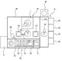
- FIG. 1 is a plan view showing a polishing apparatus according to one embodiment of the present invention
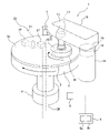
- FIG. 1 is a schematic diagram illustrating one embodiment of a polishing module
- FIG. It is a figure which shows an example of the spectrum produced
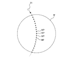
- FIG. 4 is a schematic diagram showing an example of a plurality of measurement points on the surface of a substrate
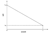
- 5 is a graph showing the relationship between the film thickness of a reference wafer and the polishing time when the polishing rate is constant
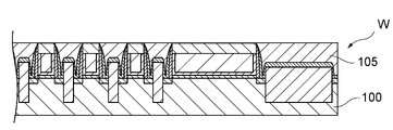
- FIG. 4 is a cross-sectional view showing an embodiment of a substrate having uneven steps
- FIG. 7A is a graph showing the relationship between the film thickness and the polishing time of a reference wafer whose polishing target film has uneven steps.
- FIG. 4 is a schematic diagram showing an example of a plurality of measurement points on the surface of a substrate
- 5 is a graph showing the relationship between the film thickness of a reference wafer and the polishing time when the polishing rate is constant
- FIG. 4 is
- FIG. 7B is a graph showing the relationship between the film thickness and the polishing time of a reference wafer whose polishing target film has uneven steps.
- 3 is a cross-sectional view of the polishing head shown in FIG. 2;
- FIG. FIG. 4 is a schematic diagram showing another embodiment of a polishing module;
- FIG. 11 is a schematic diagram showing still another embodiment of a polishing module;
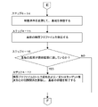
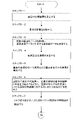
- 4 is a flow chart illustrating one embodiment of a method for polishing a reference substrate;
- 4 is a flow chart illustrating one embodiment of a method for polishing a reference substrate;
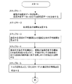
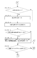
- 4 is a flow chart showing an embodiment of a method for polishing a substrate having unevenness on its surface.
- 4 is a flow chart showing an embodiment of a method for polishing a substrate having unevenness on its surface.
- FIG. 4 is a flow chart showing an embodiment of a method for polishing a substrate having unevenness on its surface.
- 4 is a flow chart showing an embodiment of a method for polishing a substrate having unevenness on its surface.
- 4 is a flow chart showing an embodiment of a method for polishing a substrate having unevenness on its surface.
- 4 is a flow chart showing an embodiment of a method for polishing a substrate having unevenness on its surface.
- FIG. 4 is a flow chart showing an embodiment of a method for polishing a substrate having unevenness on its surface.
- FIG. 4 is a diagram showing an example of a torque waveform when polishing a substrate having an uneven surface.
- FIG. 10 is a diagram showing another example of a torque waveform when polishing a substrate having uneven steps on its surface;
- FIG. 10 is a diagram showing another example of a torque waveform when polishing a substrate having uneven steps on its surface;
- FIG. 10 is a diagram showing another example of a torque waveform when polishing
- FIG. 4 is a flow chart illustrating one embodiment of a method for polishing a substrate having uneven surfaces after sufficient torque waveforms have been accumulated;
- FIG. 4 is a flow chart illustrating one embodiment of a method for polishing a substrate having uneven surfaces after sufficient torque waveforms have been accumulated;
- FIG. 4 is a flow chart illustrating one embodiment of a method for polishing a substrate having uneven surfaces after sufficient torque waveforms have been accumulated;
- FIG. 4 is a flow chart illustrating one embodiment of a method for polishing a substrate having uneven surfaces after sufficient torque waveforms have been accumulated;
- FIG. 4 is a flow chart illustrating one embodiment of a method for polishing a substrate having uneven surfaces after sufficient torque waveforms have been accumulated;
- FIG. FIG. 4 is a flow chart illustrating one embodiment of a method for polishing a substrate having uneven surfaces after sufficient torque waveforms have been accumulated;
- FIG. FIG. 4 is a flow chart illustrating one embodiment of a method for polishing a substrate
- FIG. 4 is a flow chart illustrating one embodiment of a method for polishing a substrate having uneven surfaces after sufficient torque waveforms have been accumulated;
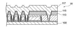
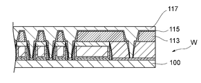
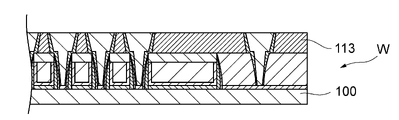
- FIG. FIG. 28A is a cross-sectional view showing another embodiment of a substrate having uneven steps on its surface.
- FIG. 28B is a cross-sectional view showing another embodiment of a substrate having uneven steps on its surface.
- FIG. 28C is a cross-sectional view showing another embodiment of a substrate having uneven steps on its surface.
- FIG. 29A is a cross-sectional view showing another embodiment of a substrate having uneven steps on its surface.
- FIG. 29B is a cross-sectional view showing another embodiment of a substrate having uneven steps on its surface.
- FIG. 29C is a cross-sectional view showing another embodiment of a substrate having uneven steps on its surface.
- FIG. 30A is a cross-sectional view showing another embodiment of a substrate having uneven steps on its surface.
- FIG. 30B is a cross-sectional view showing another embodiment of a substrate having uneven steps on its surface.
- FIG. 30C is a cross-sectional view showing another embodiment of a substrate having uneven steps on its surface.
- It is a schematic diagram which shows other embodiment of a polishing apparatus.
- FIG. 5 is a schematic diagram showing still another embodiment of a polishing apparatus;
- FIG. 5 is a schematic diagram showing still another embodiment of a polishing apparatus;
- FIG. 5 is a schematic diagram showing still another embodiment of a polishing apparatus;
- FIG. 4 is a diagram illustrating an embodiment of a method for polishing a substrate having unevenness on its surface;
- FIG. 10 is a diagram for explaining an embodiment of a polishing method for predicting elimination of steps on a substrate using a learned model
- FIG. 10 is a diagram for explaining another embodiment of a polishing method that predicts elimination of steps on a substrate using a learned model
- FIG. 10 is a diagram for explaining still another embodiment of a polishing method that predicts elimination of steps on a substrate using a learned model
- FIG. 1 is a plan view showing a polishing apparatus according to one embodiment of the invention.
- This polishing apparatus is a substrate processing apparatus capable of performing a series of steps of polishing, cleaning, and drying the surface of a substrate such as a wafer.
- the polishing apparatus has a substantially rectangular housing 60.
- the interior of the housing 60 is divided into a load/unload section 61, a polishing section 63, and a cleaning section 70 by partition walls 60a and 60b. partitioned.
- the polishing apparatus includes a film thickness measuring device 80 for measuring the film thickness of the substrate, and an operation controller 9 for controlling the operation of each component of the polishing apparatus.
- the polishing section 63 is arranged between the loading/unloading section 61 and the cleaning section 70 .
- the film thickness measuring device 80 is configured to measure the film thickness of the substrate using light interference, and can measure the film thickness profile of the substrate.
- the film thickness measuring device 80 of this embodiment is a stand-alone type film thickness measuring device.
- the film thickness measuring device 80 of this embodiment measures the film thickness of the substrate while the substrate is stationary.
- An example of such a film thickness measuring device is an ITM (In-line Thickness Monitor).
- the load/unload section 61 has a plurality of load ports 65 on which substrate cassettes containing a large number of substrates are placed.
- a loader (transport robot) 66 that can move along the row of load ports 65 is installed in the load/unload section 61 .
- the loader 66 is configured to access the substrates in the substrate cassette mounted on the load port 65 and transfer the substrates to the film thickness measuring device 80 . Furthermore, the loader 66 has the function of inverting the substrate.
- the polishing section 63 includes a polishing module 1 for polishing the surface of the substrate, a first temporary placement table 67 and a second temporary placement table 68 on which the substrate is temporarily placed, and a substrate placed in the polishing module 1 and the first temporary placement table.
- a transfer robot 69 is provided to transfer between the table 67 and the second temporary placement table 68 .
- a swing transporter 64 for transporting the substrate is arranged between the polishing section 63 and the cleaning section 70 . The substrate polished by the polishing section 63 is transported to the cleaning section 70 by the swing transporter 64 .
- the cleaning section 70 includes a first cleaning module 74, a second cleaning module 75, and a third cleaning module 76 for cleaning the substrate polished by the polishing section 63. These cleaning modules 74, 75 , 76 for drying the cleaned substrates.
- the cleaning section 70 has a linear transporter 78 that transports the substrate from the first cleaning module 74 to the second cleaning module 75, from the second cleaning module 75 to the third cleaning module 76, and from the third cleaning module 76 to the drying module 77. I have more.
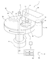
- FIG. 2 is a schematic diagram showing one embodiment of the polishing module 1.
- the polishing module 1 includes a polishing table 3 that supports a polishing pad 2, a polishing head 10 that presses a substrate (e.g., wafer) W against the polishing pad 2, and a table motor 6 that rotates the polishing table 3. , a polishing liquid supply nozzle 5 for supplying a polishing liquid such as slurry onto the polishing pad 2 , a film thickness sensor 20 , and a torque measuring device 8 .
- the upper surface of the polishing pad 2 constitutes a polishing surface 2a on which the substrate W is polished.
- the polishing module 1 includes a support shaft 14, a swing arm 16 connected to the upper end of the support shaft 14, a head shaft 11 attached to the free end of the swing arm 16, and a polishing head connected to the head shaft 11.
- a swing motor 18 connected to the motor 17 and the swing arm 16 and swinging the polishing head 10 along the polishing surface 2a is further provided.
- a polishing head 10 is connected to the lower end of a head shaft 11 .
- the polishing head motor 17 is positioned within the swing arm 16, but in one embodiment, the polishing head motor 17 may be positioned outside the swing arm 16.
- the head shaft 11 is rotatable by a polishing head motor 17.
- the polishing head 10 is connected to a swing arm 16 via a head shaft 11 .
- the rotation of the head shaft 11 causes the polishing head 10 to rotate around the head shaft 11 in the direction indicated by the arrow in the figure.
- the head shaft 11 is connected to a lifting device (not shown).
- the polishing head 10 is lifted and lowered via a head shaft 11 by an elevating device.
- the swing motor 18 is arranged within the support shaft 14 , and the swing arm 16 is configured to be able to turn (rotate) about the support shaft 14 .
- the polishing head 10 moves between a substrate W receiving position (not shown) and a position above the polishing table 2 by turning the swing arm 16 .
- the swing arm 16 may be fixed to the support shaft 14 and the swing motor 18 may be coupled to the support shaft 14 , the swing motor 18 rotating about the rotation axis of the support shaft 14 .
- 14 and swing arm 16 may be configured to rotate integrally.
- the polishing table 3 is connected to a table motor 6, and the table motor 6 is configured to rotate the polishing table 3 and the polishing pad 2 in the directions indicated by the arrows in FIG.
- the rotating directions of the polishing head 10 and the polishing table 3 are not limited to the present embodiment.
- the substrate W is polished as follows. While rotating the polishing table 3 and the polishing head 10 in the direction indicated by the arrow in FIG. The substrate W is pressed against the polishing surface 2 a of the polishing pad 2 by the polishing head 10 while being rotated by the polishing head 10 while the polishing liquid is present on the polishing pad 2 . The surface of the substrate W is polished by the chemical action of the polishing liquid and the mechanical action of the abrasive grains contained in the polishing liquid or the polishing pad 2 .
- the substrate W may be polished while the swing motor 18 swings the polishing head 10 along the polishing surface 2a within a predetermined angle range (that is, reciprocating rotational movement about the support shaft 14). good.
- An angle detector 19 is attached to the swing motor 18 to detect the rotation angle of the swing arm 16 (that is, the rotation angle of the polishing head 10 around the support shaft 14).
- the angle range of the swing motor 18 is controlled based on the angle signal from the device 19 .
- An example of the angle detector 19 is a rotary encoder.
- the operation control unit 9 includes a storage device 9a in which programs are stored, and a processing device 9b that executes operations according to instructions included in the programs.
- the processing device 9b includes a CPU (Central Processing Unit) or GPU (Graphic Processing Unit) that performs operations according to instructions included in programs stored in the storage device 9a.
- the storage device 9a comprises a main storage device (eg, random access memory) accessible by the processing unit 9b and a secondary storage device (eg, hard disk drive or solid state drive) for storing data and programs.
- the operation control section 9 is composed of at least one computer. However, the specific configuration of the operation control section 9 is not limited to this example.
- the film thickness measuring device 80, the table motor 6, the polishing liquid supply nozzle 5, the film thickness sensor 20, the torque measuring device 8, the polishing head motor 17, the swing motor 18, the angle detector 19, and the lifting device are , are electrically connected to the operation control unit 9 .
- the film thickness measuring device 80, the table motor 6, the polishing liquid supply nozzle 5, the film thickness sensor 20, the torque measuring device 8, the polishing head motor 17, the swing motor 18, the angle detector 19, and the lifting device are controlled by operation control. controlled by unit 9;
- the torque measuring device 8 is connected to the table motor 6.
- the torque measuring device 8 of this embodiment is configured to measure the torque for rotating the polishing table 3 .
- the polishing table 3 is driven by the table motor 6 so as to rotate at a constant speed. Therefore, when the torque required to rotate the polishing table 3 at a constant speed changes, the drive current of the table motor 6 changes.
- the torque for rotating the polishing table 3 is the moment of force that rotates the polishing table 3 around its axis CP.
- the torque for rotating the polishing table 3 corresponds to the driving current of the table motor 6 .
- the torque measuring device 8 is a current measuring device that measures the driving current of the table motor 6.
- torque measurement device 8 may comprise at least part of a motor driver that drives table motor 6 .
- the motor driver determines the current value required to rotate the polishing table 3 at a constant speed, and outputs the determined current value.
- the determined current value corresponds to the torque for rotating the polishing table 3 .
- a measured value of the torque (driving current of the table motor 6 ) for rotating the polishing table 3 is sent to the operation control section 9 .
- the film thickness sensor 20 is a sensor that outputs a film thickness signal that changes according to the film thickness of the substrate W.
- the film thickness signal is a numerical value or data that directly or indirectly indicates the film thickness.
- the film thickness sensor 20 of this embodiment is an optical film thickness sensor.
- the optical film thickness sensor is configured to illuminate the surface of the substrate W, measure the intensity of reflected light from the substrate W for each wavelength, and output reflected light intensity measurement data associated with the wavelength. be.
- the reflected light intensity measurement data associated with the wavelength is a film thickness signal that varies according to the film thickness of the substrate W.
- the film thickness sensor 20 includes a light source 24 that emits light, a spectroscope 27 , and an optical sensor head 21 connected to the light source 24 and the spectroscope 27 .
- the optical sensor head 21 , light source 24 and spectroscope 27 are attached to the polishing table 3 and rotate together with the polishing table 3 and polishing pad 2 .
- the position of the optical sensor head 21 is the position across the surface of the substrate W on the polishing pad 2 for each revolution of the polishing table 3 and polishing pad 2 .
- the light emitted from the light source 24 is transmitted to the optical sensor head 21 and guided from the optical sensor head 21 to the surface of the substrate W.
- the light reflects off the surface of the substrate W and the reflected light from the surface of the substrate W is received by the optical sensor head 21 and sent to the spectroscope 27 .
- a spectroscope 27 decomposes the reflected light according to wavelength and measures the intensity of the reflected light at each wavelength.
- the reflected light intensity measurement data is sent to the operation control section 9 .
- the operation control unit 9 generates a reflected light spectrum from the reflected light intensity measurement data, and determines the film thickness of the substrate W based on this spectrum.
- the spectrum of reflected light is represented as a line graph (that is, spectral waveform) showing the relationship between the wavelength and intensity of reflected light.
- the intensity of reflected light can also be expressed as a relative value such as reflectance or relative reflectance.
- FIG. 3 is a diagram showing an example of the spectrum generated by the operation control section 9.
- FIG. A spectrum is represented as a line graph (that is, a spectral waveform) showing the relationship between the wavelength and intensity of light.
- the horizontal axis represents the wavelength of light reflected from the substrate, and the vertical axis represents the relative reflectance derived from the intensity of the reflected light.
- the relative reflectance is an index value indicating the intensity of reflected light, and is the ratio of the intensity of light to a predetermined reference intensity.
- the reference intensity is the intensity of light measured in advance for each wavelength, and the relative reflectance is calculated for each wavelength. Specifically, the relative reflectance is obtained by dividing the light intensity (measured intensity) at each wavelength by the corresponding reference intensity.
- the reference intensity is obtained, for example, by directly measuring the intensity of light emitted from the optical sensor head 21, or by irradiating light onto a silicon substrate (bare substrate) on which no film is formed, and measuring the intensity of light reflected from the bare substrate. is obtained by measuring
- the dark level (background intensity obtained under the condition that light is blocked) is subtracted from the measured intensity to obtain the corrected measured intensity, and the dark level is further subtracted from the reference intensity to obtain the corrected reference intensity.
- the relative reflectance is obtained by dividing the corrected measured intensity by the corrected reference intensity.
- the relative reflectance R( ⁇ ) can be obtained using the following formula (1). where ⁇ is the wavelength of the light reflected from the substrate, E( ⁇ ) is the intensity at wavelength ⁇ , B( ⁇ ) is the reference intensity at wavelength ⁇ , and D( ⁇ ) blocks the light. is the background intensity (dark level) at wavelength ⁇ measured under the condition of
- the optical sensor head 21 guides light to the surface (surface to be polished) of the substrate W and receives reflected light from the substrate W each time the polishing table 3 rotates once.
- the reflected light is sent to spectroscope 27 .
- a spectroscope 27 decomposes the reflected light according to wavelength and measures the intensity of the reflected light at each wavelength.
- the intensity measurement data of the reflected light is sent to the operation control section 9, and the operation control section 9 generates a spectrum as shown in FIG. 3 from the intensity measurement data of the reflected light.
- the operation control unit 9 determines the film thickness of the substrate W from the spectrum of the reflected light.
- the spectrum of the reflected light changes according to the film thickness of the substrate W. FIG. Therefore, the operation control section 9 can determine the film thickness of the substrate W from the spectrum of the reflected light.
- the spectrum generated from the reflected light from the substrate W to be polished may be referred to as the measured spectrum.
- the film thickness sensor 20 of this embodiment is configured to output a plurality of intensity measurement data at a plurality of measurement points on the substrate W.
- the optical sensor head 21 while the optical sensor head 21 traverses the substrate W once, the optical sensor head 21 emits light to multiple measurement points on the substrate W and receives reflected light from these multiple measurement points.
- a plurality of optical sensor heads 21 may be provided in the polishing table 3 .
- FIG. 4 is a schematic diagram showing an example of a plurality of measurement points on the surface of the substrate W (surface to be polished).
- the optical sensor head 21 guides light to a plurality of measurement points MP each time it traverses the substrate W, and receives reflected light from these plurality of measurement points MP. Therefore, the motion control unit 9 generates a plurality of measurement spectra of reflected light from a plurality of measurement points MP each time the optical sensor head 21 crosses the substrate W (that is, each time the polishing table 3 rotates once). , determines (measures) the film thickness at each measurement point MP based on a plurality of measured spectra. The position of each measurement point MP is determined based on the light irradiation timing, the rotational speed of the polishing table 3, the position of the polishing head 10, the rotational speed of the polishing head 10, and the like.
- the operation control unit 9 is configured to determine (measure) the film thickness by comparing the measured spectrum (also referred to as film measurement data) and a plurality of reference spectra (also referred to as reference film data).
- the operation control unit 9 compares the measured spectrum generated during polishing of the substrate W with a plurality of reference spectra to determine the reference spectrum closest in shape to the measured spectrum, and associates the reference spectrum with the determined reference spectrum. Determine the film thickness obtained.
- the reference spectrum that is closest in shape to the measured spectrum is the spectrum with the smallest difference in relative reflectance between the reference spectrum and the measured spectrum.
- a plurality of reference spectra are obtained in advance while polishing a reference wafer (or reference substrate) having the same laminated structure as the substrate W to be polished (hereinafter sometimes referred to as a target wafer or target substrate).
- a reference wafer or reference substrate having the same laminated structure as the substrate W to be polished
- target wafer or target substrate
- Associated with each reference spectrum is the film thickness at which the reference spectrum was acquired. That is, each reference spectrum is acquired at different film thicknesses, and multiple reference spectra correspond to multiple different film thicknesses. Therefore, the current film thickness of the substrate W can be determined (measured) by identifying the reference spectrum that most closely resembles the measured spectrum.
- a reference wafer having the same laminated structure as the target substrate W is prepared.
- the reference wafer is transported to the film thickness measuring device 80 (see FIG. 1), and the initial film thickness of the reference wafer is measured by the film thickness measuring device 80 .
- the initial film thickness of the reference wafer is the film thickness of the reference wafer before polishing.
- the reference wafer is transferred to the polishing module 1 and is polished while slurry as a polishing liquid is supplied to the polishing pad 2 .
- the surface of the reference wafer is irradiated with light and the spectrum of reflected light from the reference wafer (ie, the reference spectrum) is obtained.
- a reference spectrum is acquired each time the polishing table 3 rotates once. Thus, multiple reference spectra are acquired during polishing of the reference wafer. After finishing the polishing of the reference wafer, the reference wafer is transported to the film thickness measuring device 80 again, and the film thickness (that is, the final film thickness) of the polished reference wafer is measured.
- the operation control unit 9 calculates the film thickness corresponding to each reference spectrum based on the relational expression showing the correlation between the film thickness of the reference wafer and the polishing time of the reference wafer. As described above, the reference spectrum is periodically acquired each time the polishing table 3 rotates once. can be calculated. That is, the operation control unit 9 can calculate the film thickness corresponding to each reference spectrum by applying the polishing time during which each reference spectrum was acquired to the above relational expression. In this way, multiple reference spectra corresponding to different film thicknesses are obtained.
- FIG. 5 is a graph showing the relationship between the thickness of the reference wafer and the polishing time when the polishing rate is constant. If the polishing rate of the reference wafer is constant, the film thickness decreases linearly with polishing time, as shown in FIG. That is, when the polishing rate of the reference wafer is constant, the above relational expression can be expressed using a linear function including the polishing rate. When the polishing rate is constant, the polishing rate can be calculated by dividing the difference between the initial film thickness Tini and the final film thickness Tfin by the polishing time t to reach the final film thickness Tfin. The operation control unit 9 determines the above relational expression based on the calculated polishing rate.
- FIG. 6 is a cross-sectional view showing an embodiment of a substrate having uneven steps.
- a stopper layer 101 made of silicon nitride (Si 3 N 4 ) is formed on the protrusions of a silicon (Si) layer 100 having uneven steps. is formed thereon.
- the polishing target film 102 of this embodiment is an insulating film made of silicon dioxide (SiO 2 ). Shallow trench isolation (STI) is an example of the stacked structure shown in FIG.
- the polishing rate differs between concave and convex portions, and it is predicted that the smaller the step, the smaller the difference in polishing rate.
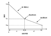
- the polishing rate of the film to be polished 102 before reaching the stepped film thickness Td is equal to the stepped film thickness Td. It becomes larger than the polishing rate after reaching. Therefore, the relational expression showing the correlation between the film thickness (thickness of the film to be polished) of the reference wafer whose film to be polished has uneven steps and the polishing time differs before and after the step elimination point.
- FIGS. 7A and 7B are graphs showing the relationship between the film thickness and the polishing time of a reference wafer whose polishing target film has uneven steps. As shown in FIGS. 7A and 7B, when the film to be polished has uneven steps, the relational expression showing the correlation between the film thickness of the reference wafer (the film thickness of the film to be polished) and the polishing time is obtained from the initial film thickness Tini.
- the film thickness corresponding to each reference spectrum is calculated based on the first relational expression and the second relational expression.
- the polishing rate from the step elimination film thickness Td to the final film thickness Tfin is constant.
- the second relational expression can be expressed using a linear function including the polishing rate.
- the polishing rate in the second relational expression is the difference between the step-removal film thickness Td and the final film thickness Tfin, which is the polishing time from the step-removal film thickness Td to the final film thickness Tfin. It can be calculated by dividing by t2.
- the operation control section 9 determines the second relational expression based on the calculated polishing rate.
- the step-removal film thickness Td is measured by the film thickness measuring device 80 when the step-removal point is reached.
- the step elimination film thickness Td is determined as follows. Until the film thickness of the reference wafer reaches the step elimination film thickness Td, the film thickness profile of the reference wafer is measured by the film thickness measuring device 80 at regular time intervals.
- the operation control unit 9 compares the film thickness of the convex portions of the measured film thickness profile (average film thickness of the convex portions) with a predetermined convex portion threshold, and determines the film thickness of the convex portions (average film thickness of the convex portions). The film thickness of the film to be polished when the average film thickness) reaches the projection threshold value is determined as the step elimination film thickness Td.
- the timing at which the film thickness of the reference wafer reaches the step elimination film thickness Td is determined by a torque current value (drive current of the table motor 6, drive current of the polishing head motor 17, or It may be detected by a change in the drive current of the swing motor 18 .
- the polishing rate is constant from the initial film thickness Tini to the step elimination film thickness Td. Therefore, the first relational expression shown in FIG. 7A can be expressed using a linear function including the polishing rate.
- the polishing rate of the first relational expression shown in FIG. 7A is obtained by dividing the difference between the initial film thickness Tini and the step-removing film thickness Td by the polishing time t1 from the initial film thickness Tini until reaching the step-removing film thickness Td. It can be calculated by The operation control section 9 determines the first relational expression based on the calculated polishing rate.
- the polishing rate gradually decreases until the step elimination film thickness Td is reached.
- An example of the determination method of the first relational expression in the example shown in FIG. 7B is shown below.
- a plurality of film thicknesses are measured by the film thickness measuring device 80 at polishing times different from each other until the stepped film thickness Td is reached.
- These multiple film thickness measurement data are plotted on a coordinate system having a vertical axis representing the film thickness and a horizontal axis representing the polishing time.
- a regression equation is determined by performing a regression analysis on these multiple data points. This regression equation is the first relational expression.
- the first relational expression in the example shown in FIG. 7B can be expressed using, for example, a quadratic function.
- the polishing rate from the step elimination film thickness Td to the final film thickness Tfin is constant, but the polishing rate from the step elimination film thickness Td to the final film thickness Tfin is , may not be constant. Therefore, in one embodiment, even if a plurality of film thicknesses are measured by the film thickness measuring device 80 at mutually different polishing times until the film thickness of the reference wafer reaches the final film thickness Tfin from the step elimination film thickness Td. good.
- These multiple film thickness measurement data are plotted on a coordinate system having a vertical axis representing film thickness and a horizontal axis representing polishing time, and regression analysis is performed on these multiple data points to determine a regression equation. , this regression equation may be used as the second relational expression.
- the second relational expression can be expressed using, for example, a quadratic function.
- the film thickness sensor 20 may be an eddy current sensor.
- the eddy current sensor detects the eddy current corresponding to the film thickness of the substrate W and outputs an eddy current signal by causing the sensor coil to pass the magnetic flux through the conductive film of the substrate W to generate an eddy current.
- the eddy current signal is a film thickness signal that varies according to the film thickness of the substrate W.
- FIG. The eddy current signal is sent to the motion controller 9 .
- the motion controller 9 determines the film thickness of the substrate W based on the eddy current signal.
- the film thickness sensor 20 detects eddy currents each time the polishing table 3 rotates once, and the film thickness sensor 20 detects eddy currents at a plurality of measurement points MP while the substrate W is traversed once, as in the embodiment described with reference to FIG. Eddy currents are detected and an eddy current signal at each measurement point MP is output.
- the motion controller 9 determines the film thickness at each measurement point MP based on the plurality of eddy current signals.
- the measured value (magnitude of the eddy current signal) of the eddy current signal detected from the target substrate is sometimes referred to as the measured eddy current value.
- the operation control unit 9 is configured to determine the film thickness from a comparison between the measured eddy current value and the reference eddy current value.
- the operation control unit 9 identifies the reference eddy current value closest to the measured eddy current value by comparing the measured eddy current value measured during polishing of the substrate W and a plurality of reference eddy current values, and performs this determination. Determine the film thickness associated with the reference eddy current value obtained.
- a reference eddy current value is a measurement of an eddy current signal detected from a reference wafer (reference substrate) having the same stack structure as the target substrate, and multiple reference eddy current values are obtained by polishing the reference wafer (reference substrate). is acquired in advance.
- the measured spectrum and the measured eddy current value may be collectively referred to as film measurement data
- the reference spectrum and reference eddy current value may be collectively referred to as reference film data.
- the film measurement data is data including the film thickness information of the target substrate acquired based on the film thickness signal from the film thickness sensor 20
- the reference film data is the film thickness signal from the film thickness sensor 20.
- This is data including film thickness information of the reference substrate acquired based on the above.
- the step of obtaining the reference eddy current values is the same as the step of obtaining the reference spectrum described above unless otherwise specified.
- the above-described reference spectrum acquisition step is also applied to the reference eddy current value acquisition step by replacing the reference spectrum with the reference eddy current value.
- Each reference eddy current value is associated with the film thickness when the reference eddy current value was obtained.
- the operation control unit 9 calculates the film thickness corresponding to each reference eddy current value based on the relational expression showing the correlation between the film thickness of the reference wafer and the polishing time of the reference wafer.
- the film thickness corresponding to each reference eddy current value is obtained by the first relational expression and the second relational expression, as in the embodiment described with reference to FIGS. calculated based on
- each reference wafer having a structure similar to that of each target substrate is polished. to obtain the reference membrane data of The operation control unit 9 determines the film thickness of each target substrate by comparing film measurement data acquired during polishing of each target substrate with a plurality of reference film data of each reference wafer corresponding to each target substrate. .
- FIG. 8 is a cross-sectional view of the polishing head 10 shown in FIG.
- the polishing head 10 includes an elastic film 45 for pressing the substrate W against the polishing surface 2a of the polishing pad 2, a head main body 13 holding the elastic film 45, and a It has an annular drive ring 42 disposed thereon and an annular retainer ring 40 fixed to the lower surface of the drive ring 42 .
- the elastic membrane 45 is attached to the lower portion of the head body 13 .
- the head body 13 is fixed to the end of the head shaft 11 , and the head body 13 , elastic membrane 45 , drive ring 42 , and retainer ring 40 are configured to rotate integrally with the rotation of the head shaft 11 .
- the retainer ring 40 and the drive ring 42 are configured to be vertically movable relative to the head body 13 .
- the head main body 13 is made of resin such as engineering plastic (for example, PEEK).
- the lower surface of the elastic film 45 constitutes a substrate pressing surface 45 a that presses the substrate W against the polishing surface 2 a of the polishing pad 2 .
- the retainer ring 40 is arranged to surround the substrate pressing surface 45 a , and the substrate W is surrounded by the retainer ring 40 .
- Four pressure chambers 46 , 47 , 48 and 49 are provided between the elastic membrane 45 and the head body 13 .
- the pressure chambers 46 , 47 , 48 and 49 are formed by the elastic membrane 45 and the head body 13 .
- the central pressure chamber 46 is circular and the other pressure chambers 47, 48, 49 are annular. These pressure chambers 46, 47, 48, 49 are arranged concentrically.
- Gas transfer lines F1, F2, F3 and F4 are connected to the pressure chambers 46, 47, 48 and 49, respectively.
- One end of the gas transfer lines F1, F2, F3, F4 is connected to a compressed gas supply (not shown) as a utility provided in the factory where the polishing apparatus is installed.
- Compressed gas such as compressed air is supplied to pressure chambers 46, 47, 48 and 49 through gas transfer lines F1, F2, F3 and F4, respectively.
- a gas transfer line F3 that communicates with the pressure chamber 48 is connected to a vacuum line (not shown) so that a vacuum can be formed in the pressure chamber 48.
- An opening is formed in a portion of the elastic film 45 that constitutes the pressure chamber 48 , and the substrate W is held by the polishing head 10 by suction by forming a vacuum in the pressure chamber 48 . Further, the substrate W is released from the polishing head 10 by supplying compressed gas to the pressure chamber 48 .
- the elastic membrane 45 is made of a rubber material having excellent strength and durability, such as ethylene propylene rubber (EPDM).
- the retainer ring 40 is an annular member that contacts the polishing surface 2a.
- the retainer ring 40 is arranged so as to surround the outer periphery of the substrate W, and prevents the substrate W from jumping out of the polishing head 10 during polishing of the substrate W. As shown in FIG.
- the upper portion of the drive ring 42 is connected to an annular retainer ring pressing device 52 .
- the retainer ring pressing device 52 applies a downward load to the entire upper surface of the retainer ring 40 via the drive ring 42, thereby pressing the lower surface of the retainer ring 40 against the polishing surface 2a.
- the retainer ring pressing device 52 includes an annular piston 53 fixed to the upper portion of the drive ring 42 and an annular rolling diaphragm 54 connected to the upper surface of the piston 53 .
- a retainer ring pressure chamber 50 is formed inside the rolling diaphragm 54 .
- the retainer ring pressure chamber 50 is connected to the compressed gas supply source via a gas transfer line F5. Compressed gas is supplied into the retainer ring pressure chamber 50 through the gas transfer line F5.
- the gas transfer lines F1, F2, F3, F4, F5 extend through a rotary joint 15 attached to the head shaft 11.
- the polishing module 1 further comprises pressure regulators R1, R2, R3, R4 and R5, which are provided in the gas transfer lines F1, F2, F3, F4 and F5 respectively. It is Compressed gas from a compressed gas supply is supplied independently into pressure chambers 46-49 and retainer ring pressure chamber 50 through pressure regulators R1-R5. Pressure regulators R 1 -R 5 are configured to regulate the pressure of compressed gas within pressure chambers 46 - 49 and retainer ring pressure chamber 50 .
- the pressure regulators R1-R5 are connected to the operation controller 9. FIG.
- the pressure regulators R1-R5 are capable of varying the internal pressures of the pressure chambers 46-49 and the retainer ring pressure chamber 50 independently of each other.
- the pressing force of the substrate W against the polishing surface 2a and the pressing force of the retainer ring 40 against the polishing pad 2 in the three regions, i.e., the central portion, the inner intermediate portion, the outer intermediate portion, and the edge portion, can be adjusted independently.
- the gas transfer lines F1, F2, F3, F4, and F5 are also connected to atmospheric release valves (not shown), so that the pressure chambers 46 to 49 and the retainer ring pressure chamber 50 can be opened to the atmosphere.
- elastic membrane 45 may form less than or more than four pressure chambers.
- FIG. 9 is a schematic diagram showing another embodiment of the polishing module 1.
- the torque measuring device 8 is connected to the polishing head motor 17 in this embodiment.
- the torque measuring device 8 of this embodiment is configured to measure the torque for rotating the polishing head 10 .
- the polishing head 10 is driven by a polishing head motor 17 through the head shaft 11 so as to rotate at a constant speed. Therefore, when the torque required to rotate the polishing head 10 at a constant speed changes, the driving current of the polishing head motor 17 changes.
- the torque measuring device 8 is located within the oscillating arm 16 , but in one embodiment the torque measuring device 8 may be located outside the oscillating arm 16 .
- the torque for rotating the polishing head 10 is the moment of force that rotates the polishing head 10 around the axis of the head shaft 11 .
- the torque for rotating the polishing head 10 corresponds to the driving current of the polishing head motor 17 .
- the torque measuring device 8 is a current measuring device that measures the driving current of the polishing head motor 17 .
- torque measurement device 8 may comprise at least part of a motor driver that drives polishing head motor 17 .
- the motor driver determines the current value required to rotate the polishing head motor 17 at a constant speed, and outputs this determined current value.
- the determined current value corresponds to the torque for rotating the polishing head 10 .
- a measured value of the torque (driving current of the polishing head motor 17 ) for rotating the polishing head 10 is sent to the operation control section 9 .
- FIG. 10 is a schematic diagram showing still another embodiment of the polishing module 1.
- the torque measuring device 8 is connected to the swing motor 18 in this embodiment.
- the torque measuring device 8 of this embodiment is configured to measure the torque for swinging the polishing head 10 along the polishing surface 2a, that is, the torque for rotating the polishing head 10 about the support shaft 14. ing.
- the swing motor 18 swings (supports) the polishing head 10 on the polishing surface 2a at a constant speed while the substrate W is being polished.
- the torque measuring device 8 is arranged inside the spindle 14, but in one embodiment, the torque measuring device 8 may be arranged outside the spindle 14.
- the torque for swinging the polishing head 10 along the polishing surface 2a is the moment of the force that causes the polishing head 10 to reciprocate around the axis of the support shaft 14.
- the torque for swinging the polishing head 10 corresponds to the driving current of the swing motor 18 .
- the torque measuring device 8 is a current measuring device that measures the driving current of the swing motor 18 .
- An alternating current is used to reciprocate the swing motor 18 at a constant speed. Therefore, in one embodiment, the torque measuring device 8 calculates the effective value of the drive current of the rocking motor 18 as an alternating current, and outputs the calculated effective value as the measured value of the driving current of the rocking motor 18.
- the torque measuring device 8 may consist of at least part of a motor driver that drives the swing motor 18 .
- the motor driver determines the current value required to reciprocate the swing motor 18 at a constant speed, and outputs the determined current value.
- the determined current value corresponds to the torque for swinging the polishing head 10 .
- the motor driver driving the oscillating motor 18 determines the rms value of the current required to reciprocate the oscillating motor 18 at a constant speed and uses this rms value to drive the oscillating motor 18. It may be output as a current value required for reciprocating rotation at a constant speed.
- a measured value of the torque (driving current of the swing motor 18) for swinging the polishing head 10 along the polishing surface 2a is sent to the operation control section 9.
- the substrate W is polished while estimating the step elimination point based on the torque waveform (the drive current waveform of the table motor 6, the drive current waveform of the polishing head motor 17, or the drive current waveform of the oscillating motor 18).
- the thickness of the substrate W is measured by the thickness gauge 80 until sufficient torque waveform data has been accumulated to estimate the thickness of the substrate W based on the current torque waveform. is polished while measuring
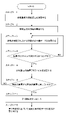
- FIGS. 11 and 12 are flowcharts showing an embodiment of a method for polishing a reference substrate
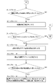
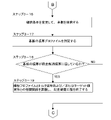
- FIGS. 13 to 18 show an embodiment of a method for polishing a substrate having uneven steps on its surface (surface to be polished). It is a flow chart.
- the flow charts shown in FIGS. 13 to 18 show the polishing method for the substrate W when sufficient torque waveform data is not accumulated.
- An example of the substrate W to be polished is the substrate shown in FIG. 6, but the substrate to be polished is not limited to the substrate shown in FIG.
- a reference substrate having the same laminated structure as the substrate W serving as the target substrate is polished.
- the polishing apparatus polishes the reference substrate while acquiring a plurality of reference film data.
- the polishing apparatus uses torque for rotating the polishing table 3 (driving current of the table motor 6) or torque for rotating the polishing head 10 around its axis (driving of the polishing head motor 17). current) or torque (driving current of the swing motor 18) for swinging the polishing head 10 along the polishing surface 2a, the substrates W as the reference substrate and the target substrate are polished.
- the motion controller 9 generates a torque waveform from the torque measurements. This torque waveform is a temporal waveform of the drive current of the motor required to move the substrate relative to the polishing surface 2a against the friction between the substrate and the polishing surface 2a of the polishing pad 2.
- this torque waveform is represented as a line graph showing the relationship between the torque for rotating the polishing table 3 (or the polishing head motor 17 or the swing motor 18) and the polishing time.
- the torque waveform of the torque for rotating the polishing table 3 the torque waveform of the torque for rotating the polishing head 10 around its axis, and the torque waveform of the torque for rotating the polishing head 10 along the polishing surface 2a.
- the torque waveform of the torque for causing the rotor to oscillate may be generically referred to simply as the torque waveform.
- step 1-1 the film thickness measuring device 80 measures the initial film thickness (film thickness before polishing) of the reference substrate.
- the film thickness measuring device 80 measures a plurality of film thicknesses (film thickness profile) at a plurality of measurement points on the reference substrate before polishing.
- step 1-2 the polishing apparatus starts polishing the reference substrate. That is, the table motor 6 rotates the polishing table 3 integrally with the polishing pad 2 at a constant rotation speed, and the polishing head 10 rotates the reference substrate at a constant rotation speed.
- the polishing head 10 further presses the reference substrate against the polishing surface 2a of the polishing pad 2 to start polishing the reference substrate.
- the reference substrate may be polished while swinging the polishing head 10 along the polishing surface 2a within a predetermined angular range by the swing motor 18 .
- step 1-3 a plurality of reference film data (reference spectra or reference eddy current values) are acquired at a plurality of measurement points on the reference substrate while polishing the reference substrate.
- the motion controller 9 periodically acquires a plurality of reference film data from a plurality of measurement points each time the film thickness sensor 20 crosses the reference substrate (that is, each time the polishing table 3 rotates once).
- a plurality of pieces of reference film data are stored in the storage device 9a of the operation control section 9.
- step 1-4 it is determined whether or not it is time to measure the film thickness profile of the reference substrate.
- the operation control unit 9 controls the current polishing time (after executing step 1-5 described later, the current polishing time and the polishing time when the film thickness profile of the reference substrate was last measured). difference) is compared with a predetermined film thickness measurement time, and when the current polishing time reaches the film thickness measurement time, polishing of the reference substrate is suspended. After that, the reference substrate is transferred to the film thickness measuring device 80, and the film thickness profile of the reference substrate is measured by the film thickness measuring device 80 (step 1-5). The film thickness profile measurement data is sent to the operation control unit 9 . If the current polishing time has not reached the film thickness measurement time, step 1-3 is executed again.
- step 1-6 the operation control unit 9 determines whether or not the film thickness of the reference substrate corresponding to the measured film thickness profile has reached the step elimination film thickness. Specifically, the operation control unit 9 compares the measured film thickness of the projections of the reference substrate (average film thickness of the projections) with a predetermined projection threshold, and determines the film thickness of the projections. When (the average film thickness of the convex portion) reaches the convex portion threshold value, it is determined that the film thickness of the reference substrate has reached the level difference elimination film thickness. When the operation control unit 9 determines that the film thickness of the substrate W has reached the level difference elimination film thickness, the polishing before the level difference elimination is finished, and step 1-7, which will be described later, is executed.
- steps 1-3 and subsequent steps are executed again.
- the film thickness profile of the reference substrate is measured a plurality of times at different polishing times until the film thickness of the reference substrate reaches the step elimination film thickness.
- the operation control unit 9 compares the thickness of the recesses (average thickness of the recesses) of the measured film thickness profile with a predetermined recess threshold, and determines the thickness of the recesses (the thickness of the recesses). average film thickness) reaches the recess threshold value, it may be determined that the film thickness of the reference substrate has reached the step elimination film thickness. Furthermore, in one embodiment, the operation control unit 9 controls the thickness of the measured film thickness profile at the convex portions (average film thickness at the convex portions) and the film thickness at the concave portions of the measured film thickness profile (average film thickness at the concave portions). thickness) is calculated, and the calculated difference is compared with a predetermined unevenness difference threshold value. can be determined to have reached
- the operation control unit 9 calculates a plurality of variations in film thickness at a plurality of measurement points on the reference substrate measured in step 1-5, are compared, and if the variation is greater than (or less than) the variation threshold value, it may be determined that the film thickness of the reference substrate has reached the level difference elimination film thickness.
- An example of the variation is the standard deviation of multiple film thicknesses at multiple measurement points.
- a torque waveform is generated during polishing of the reference substrate as described above.
- the operation control unit 9 controls the torque waveform (the torque waveform of the torque for rotating the polishing table 3, the torque waveform of the torque for rotating the polishing head 10 about its axis, or the polishing head 10 It may be determined whether or not the film thickness of the reference substrate has reached the level difference elimination film thickness based on the change in the torque waveform of the torque for oscillating along the polishing surface 2a.
- steps 1-4 and 1-5 may not be executed, and if the operation control unit 9 determines that it is not the timing to measure the film thickness profile of the reference substrate in step 1-4, step 1- 6 (that is, determination of whether or not the film thickness of the reference substrate has reached the level difference elimination film thickness based on the change in the torque waveform) may be performed.
- the operation control unit 9 calculates a differential value of the torque waveform, compares the differential value with a predetermined differential threshold value, and if the differential value is equal to or smaller than the differential threshold value, It is determined that the film thickness of the reference substrate has reached the level difference elimination film thickness.
- the differential value of the torque waveform is obtained by calculating the rate of change of torque with respect to polishing time (that is, the rate of change of torque).
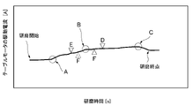
- FIG. 19 is a diagram showing an example of a torque waveform when polishing a substrate having uneven steps on its surface. Specifically, FIG. 19 shows the waveform of the driving current of the table motor 6 when polishing the substrate shown in FIG. As shown in FIG. 19, the drive current of the table motor 6 begins to rise after a certain period of time has passed since the start of polishing. This is because the contact area between the concave portion and the polishing pad 2 increases as the polishing of the convex portion of the uneven step progresses.
- a rise start point A is defined as the time point at which the drive current of the table motor 6 starts to rise.
- the slope (differential value) of the torque waveform begins to gradually decrease.
- the drive current of the table motor 6 stops increasing. Therefore, the step elimination point can be detected based on the differential value of the torque waveform.
- the driving current of the table motor 6 begins to decrease.
- An exposure start point C is defined as the point at which the underlying layer of the film to be polished begins to be exposed.
- the torque waveform has different shapes due to differences in the structure of the substrate to be polished and manufacturing variations.
- 20 and 21 are diagrams showing other examples of torque waveforms when polishing a substrate having an uneven surface. More specifically, FIG. 20 shows the waveform of the driving current of the table motor 6 when polishing a substrate having a larger proportion of the convex portion of the uneven step than the substrate in FIG. 6, and FIG. shows the waveform of the driving current of the table motor 6 when polishing a substrate deeper than the substrate in FIG.
- the operation control unit 9 determines whether the film thickness of the reference substrate has reached the level difference elimination film thickness based on the combination of the film thickness profile measured by the film thickness measuring device 80 and the differential value. It may be determined whether An example of criteria for determining whether or not the step-free film thickness is reached based on the combination of the film thickness profile and the differential value is shown below.
- the variations in the film thickness at the plural measurement points are dispersed. For example, it may be greater than (or less than) a threshold value.
- the differential value of the torque waveform is equal to or less than the differential threshold value, and based on the film thickness profile measured most recently when the differential value of the torque waveform becomes equal to or less than the differential threshold value, the film thickness of the reference substrate is eliminated.
- the film thickness profile measured immediately after the differential value of the torque waveform becomes equal to or less than the differential threshold value is determined.
- the correction value for the step elimination point may be calculated from the measurement result of the film thickness measuring device 80 .
- the differential value of the torque waveform is equal to or less than the differential threshold value, but it cannot be determined from the film thickness profile immediately after that that the film thickness of the reference substrate has reached the level difference elimination film thickness.
- the step difference elimination point is determined by adding the above difference to the polishing time at which the threshold value of the torque waveform becomes equal to or less than the differential threshold value. good too.
- the operation controller 9 generates a reference film waveform from reference film data (reference spectrum or reference eddy current value) during the polishing process of the reference substrate.
- This reference film waveform is represented as a line graph showing the relationship between the physical quantity indirectly representing the film thickness of the reference substrate included in the reference film data and the polishing time.
- the operation control unit 9 generates a reference film waveform by plotting a physical quantity that indirectly represents the film thickness of the reference substrate on a coordinate system having a vertical axis that represents the physical quantity and a horizontal axis that represents the polishing time.
- the number of peaks and bottoms decreases as polishing progresses, but the rate of decrease slows down as the point where the step is eliminated is approached.
- the physical quantity indirectly representing the film thickness of the reference substrate is the number of peaks and bottoms of the reference spectrum. Further, in one embodiment, the physical quantity is the reference eddy current value itself.
- step 1-4 and 1-5 may not be executed, and if the operation control unit 9 determines that it is not the timing to measure the film thickness profile of the reference substrate in step 1-4, step 1- 6 (that is, determination of whether or not the film thickness of the reference substrate has reached the step elimination film thickness based on the change in the reference film waveform) may be performed.
- the operation control unit 9 calculates the differential value of the reference membrane waveform, compares the differential value of the reference membrane waveform with a predetermined reference membrane threshold value, and determines the differential value of the reference membrane waveform as the reference membrane waveform. If it is less than (or more than) the film threshold value, it is determined that the film thickness of the reference substrate has reached the step elimination film thickness.
- the differential value of the reference film waveform is obtained by calculating the rate of change with respect to the polishing time of the physical quantity (that is, the rate of change of the physical quantity) that indirectly represents the film thickness of the reference substrate included in the reference film data.
- the details of the determination method based on the combination of the film thickness profile and the differential value of the reference film waveform, which are not particularly described, are that the film thickness of the reference substrate based on the combination of the above-described film thickness profile and the differential value of the torque waveform is the step elimination film thickness.
- the film The determination method based on the combination of the thickness profile and the differential value of the torque waveform can also be applied to the determination method based on the combination of the film thickness profile and the differential value of the reference film waveform.
- machine learning may be applied to the step elimination film thickness determination process based on the torque waveform and/or the reference film waveform described above. That is, the torque measuring device 9 may use a learned model constructed by performing machine learning to determine the step-removing film thickness.
- Machine learning is performed by a learning algorithm, which is an artificial intelligence (AI) algorithm, and a learned model that predicts the step-resolving film thickness is constructed by machine learning.
- a learning algorithm for constructing a trained model is not particularly limited.
- known learning algorithms such as "supervised learning”, “unsupervised learning”, “reinforcement learning”, and "neural network” can be adopted as learning algorithms.
- Deep learning is an example of neural networks. Deep learning is a machine learning method based on neural networks with multiple hidden layers (also called hidden layers).
- the operation control unit 9 generates a first relational expression indicating the correlation between the film thickness of the reference substrate up to the step elimination point and the polishing time of the reference substrate.
- the operation control unit 9 calculates the average value of the plurality of initial film thicknesses measured in step 1-1, and the plurality of film thicknesses (the plurality of steps The average value of the film thickness to be eliminated is calculated, and the difference between the average value of the initial film thickness and the average value of the uneven film thickness is calculated.
- the operation control unit 9 further divides the above difference by the polishing time from the initial film thickness to the stepped film thickness to calculate the polishing rate to the stepped point.
- the motion controller 9 generates the first relational expression based on this polishing rate. In this case, the first relational expression is generated assuming that the polishing rate up to the level difference elimination point is constant. In other words, the film thickness of the reference substrate can be obtained by multiplying the polishing time by a coefficient as the polishing rate.
- the operation control unit 9 may generate the first relational expression based on film thickness profiles measured at different polishing times. Specifically, the operation control unit 9 calculates the index value of the film thickness of the reference substrate at each polishing time from the film thickness profile measured at each polishing time. The index value is calculated, for example, by calculating the average value of a plurality of film thicknesses of the reference substrate at each polishing time. The operation control unit 9 plots the index value of each film thickness on a coordinate system having a vertical axis representing the film thickness and a horizontal axis representing the polishing time. The operation control unit 9 determines a regression formula by performing regression analysis on the plotted index values. A regression equation can be expressed using, for example, a quadratic function. The motion control unit 9 generates a first relational expression based on this regression equation. The first relational expression is stored in the storage device 9 a of the operation control section 9 .
- the operation control unit 9 assigns film thicknesses to a plurality of reference film data based on the first relational expression. That is, the operation control unit 9 calculates film thickness corresponding to a plurality of reference film data based on the first relational expression. Specifically, the operation control unit 9 calculates the film thickness corresponding to each reference film data by applying the polishing time during which each reference film data was acquired to the first relational expression.
- steps 2-1 to 2-5 a polishing process is performed after the level difference of the reference substrate is eliminated.
- the polishing apparatus starts polishing the reference substrate after eliminating the step by the method described above.
- step 2-2 a plurality of reference film data are acquired at a plurality of measurement points on the reference substrate while polishing the reference substrate by the same method as in step 1-3.
- a plurality of pieces of reference film data are stored in the storage device 9a of the operation control section 9. FIG.
- the operation control unit 9 compares the current polishing time (polishing time from step 2-1 to the present) with a predetermined end polishing time. When the operation control unit 9 determines that the current polishing time has reached the end polishing time, it ends the polishing of the reference substrate and executes step 2-4 described later. When the operation control section 9 determines that the current polishing time has not reached the final polishing time, the step 2-2 and subsequent steps are executed again.
- the final polishing time is the polishing time to reach the final film thickness, and is determined based on the step-removed film thickness, the final film thickness, and the polishing rate after step-removal.
- the polishing rate of the reference substrate after the steps are eliminated may be considered constant. In this case, since the polishing rate of the reference substrate after eliminating the unevenness is the same as the polishing rate of the reference substrate having no irregularities on the surface to be polished, it can be obtained by experiments.
- the rate is stored in advance in the storage device 9a.
- the operation control unit 9 generates a second relational expression indicating the correlation between the film thickness of the reference substrate after the step elimination point and the polishing time of the reference substrate.
- the operation control unit 9 generates a second relational expression based on the previously acquired polishing rate after step removal, the step removal film thickness, and the final film thickness.
- the second relational expression is stored in the storage device 9a of the operation control section 9.
- the operation control unit 9 assigns film thicknesses to a plurality of reference film data based on the second relational expression. That is, the operation control unit 9 calculates film thickness corresponding to a plurality of reference film data based on the second relational expression. Specifically, the operation control unit 9 calculates the film thickness corresponding to each reference film data by applying the polishing time during which each reference film data was acquired to the second relational expression.
- the polishing rate from the step elimination film thickness to the final film thickness may not be constant. Therefore, the polishing of the reference substrate may be temporarily stopped at predetermined time intervals from step 2-1 to step 2-4, and the film thickness profile of the reference substrate may be measured by the film thickness measuring device 80. FIG. Thereby, a plurality of film thickness profiles are measured at mutually different polishing times.
- the operation controller 9 may generate the second relational expression based on film thickness profiles measured at different polishing times. Specifically, the operation control unit 9 calculates the index value of the film thickness of the reference substrate at each polishing time from the film thickness profile measured at each polishing time. The index value is calculated, for example, by calculating the average value of a plurality of film thicknesses of the reference substrate at each polishing time.
- the operation control unit 9 plots the index value of each film thickness on a coordinate system having a vertical axis representing the film thickness and a horizontal axis representing the polishing time.
- the operation control unit 9 determines a regression formula by performing regression analysis on the plotted index values.
- a regression equation can be expressed using, for example, a quadratic function.
- the operation control section 9 may generate a second relational expression based on this regression expression.
- the final thickness of the reference substrate may be determined based on the thickness profile measured by the thickness gauge 80 .
- the operation control unit 9 controls the film thickness of the reference substrate measured by the film thickness measuring device 80 (for example, the average value of a plurality of film thicknesses at a plurality of measurement points on the reference substrate) and a predetermined When the thickness of the reference substrate has reached the target thickness, it may be determined that the thickness of the reference substrate has reached the final thickness.
- the polishing process of the substrate W as the target substrate is performed.
- An embodiment of a method for polishing a substrate W in a state in which sufficient torque waveform data is not accumulated will be described below with reference to FIGS. 13 to 18 .
- steps 3-1 to 3-19 see FIGS. 13 to 15
- polishing is stopped at fixed time intervals, and the film thickness of the reference substrate is measured by the film thickness measuring device 80.
- FIG. A step polishing process is performed in steps 3-1 to 3-19.
- the stepped polishing step is a step of polishing the substrate W before the film thickness of the substrate W reaches the stepped film thickness. determining a plurality of film thicknesses at a plurality of measurement points of the.
- a torque waveform is generated from the torque measurement values described above, and data of the torque waveform and/or the target film waveform, which will be described later, is stored in the storage device 9a.
- the film thickness measuring device 80 measures the initial film thickness (film thickness before polishing) of the substrate W.
- the film thickness measuring device 80 measures a plurality of film thicknesses (film thickness profile) at a plurality of measurement points on the substrate W before polishing.
- the polishing apparatus starts polishing the substrate W by the method described above. That is, the table motor 6 rotates the polishing table 3 together with the polishing pad 2 at a constant rotation speed, and the polishing head 10 rotates the substrate W at a constant rotation speed.
- the polishing head 10 further presses the substrate W against the polishing surface 2a of the polishing pad 2 to start polishing the substrate W.
- the substrate W may be polished while the swing motor 18 swings the polishing head 10 along the polishing surface 2a within a predetermined angular range.
- step 3-3 while polishing the substrate W, a plurality of film measurement data (measured spectra or measured eddy current values) are acquired at a plurality of measurement points on the substrate W, and a plurality of film measurement data and a plurality of reference film data are obtained. and reference film data (reference spectrum or reference eddy current value) corresponding to each film measurement data (that is, the reference spectrum closest to the measured spectrum (the error with the measured spectrum is Determine (select) the reference eddy current value that is closest to the measured eddy current value (the reference eddy current value that has the least error with the measured eddy current value)).
- reference film data reference spectrum or reference eddy current value
- the operation control unit 9 determines the film thickness at each measurement point. That is, the operation control unit 9 controls the film thickness of the reference film data determined in step 3-3 to be the film thickness of the reference film data calculated based on the first relational expression (the film thickness corresponding to the reference film data). thickness) is applied to the film thickness at each measurement point. That is, the operation control unit 9 causes the film thickness of the reference film data determined in step 3-3, which is calculated based on the first relational expression, to correspond to the reference film data. It is determined as the film thickness at the measurement point where the film measurement data was acquired.
- the operation control unit 9 issues instructions to the plurality of pressure regulators R1 to R4 based on the film thickness at the plurality of measurement points on the substrate W to adjust the polishing profile of the substrate W.
- step 3-5 the operation control unit 9 controls each of the plurality of regions of the substrate W (in this embodiment, four regions, namely, the central portion, the inner intermediate portion, the outer intermediate portion, and the edge portion).
- An average film thickness and an average film thickness of the entire substrate W are calculated.
- the average film thickness for each region is the average value of film thicknesses at a plurality of measurement points in each region, and the average film thickness of the entire substrate W is the average value of film thicknesses at all measurement points on the substrate W. be.
- the operation control unit 9 issues a command to the pressure regulators R1 to R4 to reduce the difference between the average film thickness of the entire substrate W and the average film thickness of each of the plurality of areas. , the pressing force against the polishing surface 2a of the substrate W in each corresponding region of the substrate W is adjusted independently.
- the operation control unit 9 compares the average film thickness of each region with the average film thickness of the entire substrate W, and when the film thickness of a certain region is larger than the average film thickness of the entire substrate W, the operation control unit 9 commands the pressure regulator associated with that region (eg, pressure regulator R1 for the central portion) to increase the internal pressure of the corresponding pressure chamber (eg, pressure chamber 46).
- step 3-7 feature points of the torque waveform and/or the target membrane waveform are detected.
- the feature point is, for example, a point where the slope of the waveform changes beyond a threshold value, which is point B in FIGS.
- the operation controller 9 generates a target film waveform from film measurement data (measured spectrum or measured eddy current value).
- This target film waveform is represented as a line graph showing the relationship between the physical quantity indirectly representing the film thickness of the substrate W contained in the film measurement data and the polishing time.
- the motion control unit 9 generates a target film waveform by plotting a physical quantity indirectly representing the film thickness of the substrate W on a coordinate system having a vertical axis representing the physical quantity and a horizontal axis representing the polishing time.
- the measured spectrum shows that the number of peaks and bottoms decreases as polishing progresses, but the rate of decrease slows down as it approaches the step elimination point.
- the physical quantity that indirectly represents the film thickness of the substrate W is the number of peaks and bottoms in the measured spectrum. Further, in one embodiment, the physical quantity is the reference eddy current value itself.
- step 3-8 the polishing of the substrate W is suspended, and the film thickness profile of the substrate W is measured by the film thickness measuring device 80.
- the film thickness profile of the substrate W is measured a plurality of times at different polishing times until the film thickness of the substrate W reaches the step elimination film thickness.
- step 3-9 the correlation between the film thickness profile of the substrate W and the torque waveform and/or the target film waveform is confirmed, and it is determined whether or not the film thickness of the substrate W has reached the step elimination film thickness.
- the step polishing process is terminated (step 3-10).
- the operation control unit 9 determines that the film thickness of the substrate W has not reached the level difference elimination film thickness, the operation control unit 9 sets the film thickness profile (remaining film profile) of the substrate W to a predetermined standard (specification). (step 3-11).
- step 3-12 if it is determined that the residual film profile satisfies the specification, polishing of the substrate W is continued under the current polishing conditions. At step 3-12, processes similar to steps 3-3 to 3-7 are executed.
- step 3-13 the polishing of the substrate W is suspended, and the film thickness profile of the substrate W is measured by the film thickness measuring device 80.
- step 3-14 it is determined whether or not the film thickness of the substrate W has reached the level difference elimination film thickness by the same method as in step 3-9.
- the motion control unit 9 determines that the film thickness of the substrate W has reached the level difference elimination film thickness
- the correlation between the film thickness profile and the torque waveform and/or the target film waveform is stored in the storage device 9a of the motion control unit 9. Then, the stepped polishing process is completed (step 3-15).
- step 3-11 if the operation control unit 9 determines that the residual film profile does not satisfy the specifications, the polishing conditions are changed so as to improve the residual film profile (to satisfy the above criteria), and the substrate W is removed.
- Polish step 3-16.
- An example of the polishing conditions is the internal pressure of each pressure chamber.
- the operation control unit 9 issues a command to at least one of the pressure regulators R1 to R4 to increase (or decrease) the internal pressure of the corresponding pressure chamber.
- step 3-17 the polishing of the substrate W is suspended, and the film thickness profile of the substrate W is measured by the film thickness measuring device 80.
- step 3-18 it is determined whether or not the film thickness of the substrate W has reached the level difference elimination film thickness by the same method as in step 3-9.
- the motion control unit 9 determines that the film thickness of the substrate W has reached the level difference elimination film thickness
- the correlation between the film thickness profile and the torque waveform and/or the target film waveform is stored in the storage device 9a of the motion control unit 9.
- the stepped polishing process is completed (step 3-19).
- step 3-18 when the operation control unit 9 determines that the film thickness of the substrate W has not reached the level difference elimination film thickness, the process returns to step 3-11.
- step 3-11 after changing the polishing conditions once, the step of determining whether the residual film profile satisfies the specification (step 3-11) may be omitted. That is, when the operation control unit 9 determines in step 3-18 that the film thickness of the substrate W has not reached the level difference elimination film thickness, the process may return to step 3-12.
- the planarization step includes determining a plurality of film thicknesses at a plurality of measurement points on the substrate W based on the film thickness of the reference film data calculated based on the second relational expression. Steps 4-1 to 4-17, which are not specifically described, are the same as steps 3-3 to 3-19.
- step 4-2 the operation control unit 9 controls the film thickness of the reference film data determined in step 4-1 and calculated based on the second relational expression (reference film data The film thickness corresponding to ) is applied to the film thickness at each measurement point. That is, the operation control unit 9 causes the film thickness of the reference film data determined in step 4-1, which is the film thickness of the reference film data calculated based on the second relational expression, to correspond to the reference film data. It is determined as the film thickness at the measurement point where the film measurement data was acquired.
- a more specific process of step 4-2 is the same as step 3-4 except that the film thickness corresponding to the reference film data is determined based on the second relational expression.
- the operation control unit 9 compares the film thickness of the substrate W with a predetermined final film thickness (target film thickness). When the film thickness of the substrate W reaches the final film thickness, the polishing end point is determined as the time point when the film thickness reaches the final film thickness, and the polishing of the substrate W is finished (step 4-8). Specifically, the operation control unit 9 compares the average film thickness of the entire substrate W with a predetermined final film thickness. When the average film thickness of the entire substrate W reaches the final film thickness, the polishing of the substrate W is terminated.
- target film thickness target film thickness
- step 4-7 the operation control unit 9 sets the current polishing time (polishing time from step 4-1 to the present time) to a predetermined end.
- the final polishing time is the polishing time to reach the final film thickness, and is determined based on the stepped film thickness, the final film thickness, and the polishing rate after the stepped film is removed.
- steps 4-12 and 4-16 the same process as step 4-7, that is, the process of comparing the film thickness of the substrate W with a predetermined final film thickness is performed.
- steps 4-13 and 4-17 the correlation between the film thickness profile and the torque waveform and/or the target film waveform is accumulated in the storage device 9a of the operation control unit 9, and polishing of the substrate W is completed.
- the operation control unit 9 associates the measured film thickness profile of the substrate W with the torque waveform and/or the target film waveform.
- the motion controller 9 may determine the step elimination point B based on the measured film thickness profile of the substrate W.
- the operation control section 9 may determine the step elimination point B of the torque waveform based on the polishing time when the film thickness of the substrate W reaches the step elimination film thickness.
- the operation control unit 9 converts the torque waveform and/or the target film waveform into the initial film thickness data of the substrate W measured by the film thickness measuring device 80, the film thickness profile of the substrate W before polishing, and the substrate during polishing. It is stored in the storage device 9a in association with the film thickness profile of W, the stepped film thickness, and the like.
- the polishing apparatus processes a plurality of substrates of the same type with variations in the initial film thickness and a plurality of substrates with different shapes of uneven structures while generating torque waveforms in steps 3-1 to 3-19 and steps 4-1 to 4-1. 4-17, and based on the film thickness profile measured during the polishing process of each substrate, the step elimination point of each torque waveform may be determined.
- the operation controller 9 may associate each torque waveform and/or target film waveform generated during polishing of each substrate with the film thickness data of the substrate to be polished. Examples of the film thickness data include the type of substrate to be polished, the initial film thickness data of the substrate to be polished, the film thickness profile of the substrate before polishing, the film thickness profile of the substrate during polishing, and the stepped film thickness data.
- a plurality of torque waveforms (drive current waveform of the table motor 6, drive current waveform of the polishing head motor 17, or drive current waveform of the oscillating motor 18) associated with these film thickness data and/or target film Waveform data is stored in the storage device 9a.
- the motion controller 9 associates the torque waveform and/or the reference film waveform generated during polishing of the reference substrate with the film thickness data of the reference substrate.
- the data of the torque waveform (the drive current waveform of the table motor 6, the drive current waveform of the polishing head motor 17, or the drive current waveform of the oscillating motor 18) associated with the film thickness data and/or the data of the reference film waveform are stored in a storage device. 9a.
- 22 to 27 are flow charts showing an embodiment of a method for polishing a substrate having unevenness on its surface after a sufficient torque waveform has been accumulated.
- the substrate is polished while estimating the step elimination point based on the torque waveform.
- An example of the substrate W to be polished is the substrate shown in FIG. 6, but the substrate W to be polished is not limited to the substrate shown in FIG.
- the polishing apparatus uses torque for rotating the polishing table 3 (driving current of the table motor 6) or torque for rotating the polishing head 10 around its axis (power of the polishing head motor 17).
- the substrate W as the reference substrate and the target substrate is polished while measuring the driving current) or the torque for swinging the polishing head 10 along the polishing surface 2a (the driving current of the swing motor 18).
- the operation control unit 9 generates a torque waveform from the measured torque.
- the torque waveform acquired before polishing in this embodiment and stored in the storage device 9a may be referred to as a reference torque waveform.
- the motion controller 9 may generate the target film waveform during the polishing process of the substrate W.
- the reference film waveform and the target film waveform acquired before polishing in this embodiment and stored in the storage device 9a may be referred to as accumulated film waveforms.
- a step polishing process is performed in steps 5-1 to 5-21 (see FIGS. 22 to 24). Steps 5-1 to 5-6, which are not specifically described, are the same as steps 3-1 to 3-6.
- the film thickness measuring device 80 measures the initial film thickness of the substrate W to be polished (film thickness profile of the substrate W before polishing). Based on the measurement data of the film thickness measuring device 80 (the film thickness profile of the substrate W before polishing) and the type of the substrate W, the operation control unit 9 selects one waveform from a plurality of reference torque waveforms (or a plurality of accumulated film waveforms). Select a reference torque waveform (or one accumulated film waveform). Specifically, the operation control unit 9 compares the measurement data of the film thickness measuring device 80 and the type of substrate W with the film thickness data and the type of substrate associated with each reference torque waveform (or each accumulated film waveform). do.
- the operation control unit 9 controls the measurement data of the film thickness measurement device 80 and the film thickness data (specifically, the pre-polishing data of the substrate used to generate the reference torque waveform or the accumulated film waveform) for the same type of substrate.
- the reference torque waveform with the closest film thickness profile is selected as the reference torque waveform.
- the operation control unit 9 controls the measurement data of the film thickness measuring device 80 and the film thickness data (specifically, the pre-polishing data of the substrate used to generate the accumulated film waveform) for the same type of substrate. ) may be selected as the reference film waveform.
- the torque waveform selected in step 5-1 will be referred to as a reference torque waveform
- the selected accumulated film waveform will be referred to as a reference film waveform.
- the operation control unit 9 determines the film thickness at each measurement point. That is, the operation control unit 9 controls the film thickness of the reference film data determined in step 5-3 to be the film thickness of the reference film data calculated based on the first relational expression (the film thickness corresponding to the reference film data). thickness) is applied to the film thickness at each measurement point. That is, the operation control unit 9 causes the film thickness of the reference film data determined in step 5-3, which is calculated based on the first relational expression, to correspond to the reference film data. It is determined as the film thickness at the measurement point where the film measurement data was acquired.
- step 5-7 feature points of the torque waveform and/or the target membrane waveform are detected.
- step 5-8 it is checked whether there is any abnormality in the torque waveform and/or the target film waveform.
- the torque waveform and/or the target film waveform are compared with the film thickness profile accumulated in steps 5-12, 5-17, and 5-21, which will be described later, and the correlation between the torque waveform and/or the target film waveform. Alternatively, it may be determined whether there is an abnormality in the target film waveform. If the operation control unit 9 determines that there is no abnormality in the waveform, the step polishing process is terminated (step 5-9). If the operation control section 9 determines that the waveform is abnormal, the steps 5-10 and after are executed.
- step 5-10 the polishing of the substrate W is suspended, and the film thickness profile of the substrate W is measured by the film thickness measuring device 80.
- steps 5-7 through 5-10 may not be performed, and step 5-11 may be performed after step 5-6. Further, in one embodiment, step 5-11 may be performed after step 5-7.
- the operation control unit 9 determines whether or not the film thickness of the substrate W has reached the step elimination film thickness, ie, whether or not the step polishing process should be terminated. Specifically, the operation control unit 9 compares the torque waveform (or target film waveform) generated during polishing with the reference torque waveform (or reference film waveform), and determines whether the film thickness of the substrate W has reached the step elimination film thickness. It is determined whether or not the stepped polishing process should be terminated. When the motion control unit 9 determines that the stepped polishing process should be terminated, the motion control unit 9 accumulates the correlation between the film thickness profile and the torque waveform and/or the target film waveform in the storage device 9a of the motion control unit 9, and starts the stepped polishing step. (step 5-12). In one embodiment, if the torque waveform or the target film waveform is abnormal, profile adjustment of the waveform may be performed after the step polishing step is completed.
- step 5-11 The details of step 5-11 are as follows. Specifically, the operation control unit 9 controls the current torque of the generated torque waveform (or target film waveform) (or the current physical quantity, that is, the physical quantity indirectly representing the film thickness of the substrate W included in the film measurement data). ) reaches the step elimination point estimated from the reference torque waveform (or the reference film waveform), it is determined that the step polishing process should be terminated.
- the step polishing process may be terminated even if the current torque (or current physical quantity) has not reached the step elimination point. For example, when the magnitude of the current torque (or the current physical quantity) becomes equal to or less than a predetermined percentage (for example, 130% or less) of the reference level of the reference torque waveform (or the reference membrane waveform), and/ Alternatively, it may be determined that the step polishing process should be terminated when the current polishing time reaches 90% or more of the polishing time at the step elimination point estimated from the reference torque waveform (or the reference film waveform).
- the reference level is a predetermined torque (or physical quantity) magnitude threshold.
- the operation control unit 9 controls that the magnitude of the current torque (or the current physical quantity) becomes equal to or less than a predetermined percentage of the reference level of the amount of change in the reference torque waveform differential value (or the reference film waveform differential value). and/or when the current polishing time reaches 90% or more of the polishing time at the step difference elimination point estimated from the amount of change in the reference torque waveform differential value (or the reference membrane waveform differential value), the step polishing process is started. You may decide to terminate.
- the reference level is a predetermined threshold value of the amount of change in the torque waveform differential value (differential value of physical quantity).
- the operation control unit 9 controls the shape of the generated torque waveform (or target film waveform) and the polishing time corresponding to the current polishing time of the reference torque waveform (or reference film waveform). may be compared and the degree of matching between these shapes may be calculated.
- the operation control unit 9 compares the calculated matching degree with a predetermined reference matching degree, and if the calculated matching degree is equal to or higher than the predetermined reference matching degree, the step estimated from the reference torque waveform (or the reference film waveform) The difference between the polishing time at the elimination point and the current polishing time is calculated, and when the polishing time of the substrate W reaches the current polishing time plus the above difference or a value obtained by multiplying the difference by a coefficient. , it may be determined that the step polishing process should be terminated.
- the degree of matching is represented by a numerical value from 0 to 1, and the closer to 1, the higher the degree of matching.
- the reference matching degree is, for example, 0.8.
- the operation control unit 9 determines that a polishing abnormality has occurred, and suspends the polishing of the substrate W. good too. After that, the substrate W may be transported to the film thickness measuring device 80 and the film thickness profile of the substrate W may be measured by the film thickness measuring device 80 .
- the operation control section 9 may issue a command to change the polishing conditions to the polishing apparatus.
- the operation control section 9 may issue a command to at least one of the pressure regulators R1 to R4 to increase (or decrease) the internal pressure of the corresponding pressure chamber.
- step polishing process may be terminated.
- the method described in step 3-9 ie, a method similar to step 1-6, may be used to determine whether the step polishing process should be terminated.
- step 5-11 when the motion control unit 9 determines that the film thickness of the substrate W has not reached the stepped film thickness, the motion control unit 9 sets the film thickness profile (remaining film profile) of the substrate W in advance. It is determined whether or not the specified criteria (specs) are satisfied (step 5-13).
- step 5-14 if it is determined that the residual film profile satisfies the specifications, the polishing of the substrate W is continued under the current polishing conditions. At step 5-14, processes similar to steps 5-3 to 5-7 are executed.
- step 5-15 the polishing of the substrate W is suspended, and the film thickness profile of the substrate W is measured by the film thickness measuring device 80.
- step 5-16 it is determined whether or not the film thickness of the substrate W has reached the level difference elimination film thickness by the same method as in step 5-11.
- the motion control unit 9 determines that the film thickness of the substrate W has reached the level difference elimination film thickness
- the correlation between the film thickness profile and the torque waveform and/or the target film waveform is stored in the storage device 9a of the motion control unit 9. Then, the stepped polishing process is completed (step 5-17).
- step 5-13 if the motion control unit 9 determines that the residual film profile does not satisfy the specifications, the polishing conditions are changed so as to improve the residual film profile (to satisfy the above criteria), and the substrate W is removed.
- Polish step 5-18.
- An example of the polishing conditions is the internal pressure of each pressure chamber.
- the operation control unit 9 issues a command to at least one of the pressure regulators R1 to R4 to increase (or decrease) the internal pressure of the corresponding pressure chamber.
- step 5-19 the polishing of the substrate W is suspended, and the film thickness profile of the substrate W is measured by the film thickness measuring device 80.
- step 5-20 it is determined whether or not the film thickness of the substrate W has reached the level difference elimination film thickness by the same method as in step 5-11.
- the motion control unit 9 determines that the film thickness of the substrate W has reached the level difference elimination film thickness
- the correlation between the film thickness profile and the torque waveform and/or the target film waveform is stored in the storage device 9a of the motion control unit 9.
- the stepped polishing process is completed (step 5-21).
- step 5-20 if the operation control section 9 determines that the film thickness of the substrate W has not reached the level difference elimination film thickness, the process returns to step 5-13.
- step 5-13 after changing the polishing conditions once, the step of determining whether the residual film profile satisfies the specification (step 5-13) may be omitted. That is, when the operation control unit 9 determines in step 5-20 that the film thickness of the substrate W has not reached the step elimination film thickness, step 5-14 and subsequent steps may be executed.
- steps 5-16 and 5-20 may be performed after steps 5-14 and 5-18 without performing steps 5-15 and 5-19. Further, in one embodiment, when step 5-10 is not executed and the operation control unit 9 determines in step 5-11 that the film thickness of the substrate W has not reached the step-removal film thickness, step 5 After -11, steps 5-14 to 5-17 may be executed. In this case, step 5-15 may be omitted.
- the planarization step includes determining a plurality of film thicknesses at a plurality of measurement points on the substrate W based on the film thickness of the reference film data calculated based on the second relational expression.
- step 6-2 the operation control unit 9 calculates the film thickness of the reference film data determined in step 6-1, which is calculated based on the second relational expression, at each measurement point. applied to the film thickness of That is, the operation control unit 9 associates the film thickness of the reference film data determined in step 6-1, which is the film thickness of the reference film data calculated based on the second relational expression, with the reference film data. It is determined as the film thickness at the measurement point where the film measurement data was acquired.
- a more specific process of step 6-2 is the same as step 5-4 except that the film thickness corresponding to the reference film data is determined based on the second relational expression.
- the operation control unit 9 compares the film thickness of the substrate W with a predetermined final film thickness (target film thickness). When the film thickness of the substrate W reaches the final film thickness, the polishing end point is determined as the time point when the film thickness reaches the final film thickness, and the polishing of the substrate W is finished. Specifically, the operation control unit 9 compares the average film thickness of the entire substrate W with a predetermined final film thickness. When the average film thickness of the entire substrate W reaches the final film thickness, the polishing of the substrate W is terminated.
- target film thickness target film thickness
- the operation control unit 9 determines the current polishing time (polishing from step 6-1 to the present time) is compared with a predetermined end polishing time, and if it is determined that the current polishing time has reached the end polishing time, the polishing of the substrate W may be ended.
- the final polishing time is the polishing time to reach the final film thickness, and is determined based on the stepped film thickness, the final film thickness, and the polishing rate after the stepped film is removed.
- steps 6-10, 6-15, and 6-19 the correlation between the film thickness profile and the torque waveform and/or the target film waveform is stored in the storage device 9a of the operation control unit 9, and polishing of the substrate W is finished. do.
- step 6-9 may be executed after step 6-4 without executing steps 6-5 to 6-8. Further, in one embodiment, step 6-9 may be performed after step 6-5. Further, in one embodiment, steps 6-13 and 6-17 may not be performed, and steps 6-12 and 6-16 may be followed by steps 6-14 and 6-18.
- the polishing apparatus of this embodiment changes the relational expression used when determining the film thickness of the substrate W being polished according to the surface shape of the substrate W. Further, the polishing apparatus compares the torque waveform generated during polishing with the reference torque waveform acquired before polishing, and determines the timing of changing the above relational expression. As a result, even when the substrate has an uneven surface, the film thickness of the substrate being polished can be measured with high accuracy. As a result, it is possible to improve the uniformity of the film thickness and the end point detection performance.
- the first The relational expression and/or the second relational expression may be corrected.
- the reference substrate may be polished using steps similar to those described with reference to FIGS. 11 and 12 to regenerate the first and/or second relations.
- FIGS. 28 to 30 are cross-sectional views showing another embodiment of a substrate W having uneven steps on its surface.
- 28A, 29A, and 30A show the state of each substrate before polishing
- FIGS. 28C, 29C, and 30C show the state when each substrate is polished to the polishing end point.
- FIG. 28 shows a cross section of the replacement gate.
- the substrate W shown in FIG. 28 is composed of a silicon (Si) layer 100 having uneven steps, an insulating film 105 formed above the silicon layer 100, and titanium nitride (TiN) formed on the insulating film 105. It has a liner film 107 and a tungsten (W) film 109 formed on the liner film 107 . Since the tungsten (W) film 109 is a metal film, an eddy current sensor is used as the film thickness sensor 20 when polishing the substrate W shown in FIG.
- FIG. 29 shows a cross-section of a SAC (Self Aligned Contact) nitride.
- SAC Self Aligned Contact
- FIG. 30 shows a cross section of the contact portion.
- the substrate W shown in FIG. 30 includes a silicon (Si) layer 100, an insulating film 113 formed above the silicon layer 100, and a liner film 115 made of titanium nitride (TiN) formed on the insulating film 113. , and a tungsten (W) film 117 formed on the liner film 115 .
- Si silicon
- TiN titanium nitride
- W tungsten
- FIG. 31 is a schematic diagram showing another embodiment of the polishing apparatus. Since the configuration and operation of this embodiment, which are not specifically described, are the same as those of the embodiment shown in FIGS. 1 to 27, redundant description thereof will be omitted. In FIG. 31, illustration of some components is omitted.
- the film thickness measuring device 80 is attached to the polishing table 3 .
- the film thickness measuring device 80 of this embodiment is made smaller than the film thickness measuring device 80 described with reference to FIG.
- the film thickness measuring instrument 80 of this embodiment includes a light projecting section 82 that irradiates the substrate W with light, and a light receiving section 85 that receives reflected light reflected by the surface of the substrate W (surface to be polished).
- the light projecting section 82 includes a light source (not shown) that emits light.
- the light projecting part 82 is arranged so as to irradiate the substrate W with light obliquely from below, and the light receiving part 85 is arranged obliquely with respect to the surface of the substrate W.
- the arrangement of the portion 82 and the light receiving portion 85 is not limited to this arrangement.
- the film thickness measurement device 80 may be an eddy current film thickness measurement device that includes an eddy current sensor instead of the light emitter 82 and the light receiver 85 .
- an ellipsometer is used as the film thickness measuring device 80 .
- the principle of the ellipsometer is a commonly known principle.
- the film thickness measuring device 80 supplies a gas such as CDA (clean dry air), nitrogen (N 2 ), argon (Ar), air, etc. to the surface of the substrate W to dry the measuring part. It further comprises a nozzle 87 and a waste liquid path 89 for discharging a liquid used for polishing such as a polishing liquid (for example, slurry).
- the substrate W Since the substrate W is supported by the polishing head 10, it can be rotated and moved in the X/Y directions, and the film thickness distribution can be obtained by measuring a plurality of arbitrary points on the substrate W while rotating the substrate W. becomes possible. In order to protect the surface condition of the substrate W, it is possible to immerse the substrate W except for the measuring portion.
- the light projecting part 82 , the light receiving part 85 , the gas supply nozzle 87 and the waste liquid passage 89 are attached to the polishing table 3 and rotate together with the polishing table 3 and the polishing pad 2 .
- the light projecting section 82 emits light to a plurality of measurement points on the rotating substrate W, and the light receiving section 85 measures these plurality of measurement points. Receive reflected light from a point.
- the film thickness measuring device 80 is an eddy current type film thickness measuring device, the eddy current sensor generates eddy currents at a plurality of measurement points on the substrate W and detects the eddy currents at these plurality of measurement points.
- the film thickness measuring device 80 may be arranged in the center of the polishing table 3 as shown in FIG.
- the film thickness and film thickness profile of the substrate W can be measured by the film thickness measuring device 80 without removing the substrate W from the polishing head 10 .
- time loss due to removal of the substrate W can be reduced (throughput is improved), positional and tilt deviations due to re-installation of the substrate W can be prevented, measurement coordinate errors can be reduced, rework after measurement is easy, and end point detection sensors can be used.
- Thiickness sensor 20 Advantages such as improvement in output calibration accuracy and reduction in adhesion of particles due to detachment/transfer of the substrate W can be obtained.
- the film thickness measuring device 80 can be combined with the detection of the step elimination point using the drive currents of the table motor 6, the polishing head motor 17, and the swing motor 18, and the detection of the end point using the film thickness sensor 20. can be done.
- the film thickness sensor 20 sensor it is necessary to calibrate the film thickness sensor 20 .
- calibration is required to determine the correlation between the substrate W whose film thickness has been measured and the output of the end point detection sensor. If the film thickness measurement device 80 is an ITM (ex-situ film thickness measurement device) installed away from the polishing module 1, the substrate W is removed from the polishing head 10 during this calibration, and transport robots 66, 69, etc. Transported to ITM.
- the film thickness measuring device 80 is an ITM installed away from the polishing module 1, it is necessary to measure the film thickness measurement position error, polish multiple times, measure the ITM film thickness, and acquire the output of the film thickness sensor 20 at multiple points. Although an error factor occurs when there is such an error factor, such an error factor can be reduced in the present embodiment. Therefore, it is possible to perform calibration with higher accuracy than in the past, and it is also possible to improve the end point detection accuracy.
- the present embodiment it is possible to determine the film thickness distribution and accuracy based on the film measurement results obtained by specifying the area of the high-density wiring portion of the substrate W. Since it is not necessary to remove the substrate W from the polishing head 10, after measuring the correlation between the coordinates of the substrate W and the film thickness, it is possible to compare the output signal of the film thickness sensor 20 with a small coordinate position error. It is possible to obtain the relationship between the change in the signal of the film thickness sensor 20, the coordinate position of the substrate W, and the film thickness with higher accuracy. In the case of a wafer with a complicated pattern structure, it can be used effectively. For example, the present embodiment may be used for film measurement or the like using only waveforms in the effective region.
- the present embodiment is also applicable to various process pattern films such as oxide films, nitride films, metal films, mixed pattern films thereof, STI and SAC process films, and the like.
- a film thickness measurement device 80 described with reference to FIGS. 31 and 32 a film thickness measurement device using a camera image processing method, a multispectral camera, or a hyperspectral camera may be used.
- a film thickness measuring device using image processing or an optical interference method may be used as the film thickness measuring device 80 .
- a film thickness measuring device 80 may be installed beside (near) the polishing table 3 .
- the measurement can be performed without liquid immersion.
- the measuring equipment and mechanism may be composed of MEMS (Micro Electro Mechanical Systems).
- the connection between the light projecting section 82 and the light receiving section 85 can be a direct connection type or a fiber connection type.
- the film thickness measuring device 80 As an advantage of installing the film thickness measuring device 80 in the polishing table 3 or in the vicinity of the polishing table 3 , it is not necessary to remove the substrate W from the polishing head 10 , and the film thickness can be measured while the substrate W is mounted on the polishing head 10 . measurement becomes possible.
- Other advantages include reduction in time loss (improvement in throughput) due to removal of the substrate W from the polishing head 10, reduction in positional and tilt deviation of the substrate W due to reinstallation of the substrate W on the polishing head 10, reduction in measurement coordinate error, measurement The substrate W can be easily reworked later, the calibration accuracy of the end-point detection sensor output can be improved, and the adhesion of particles during detachment/transport can be reduced.
- FIG. 34 is a cross-sectional view showing still another embodiment of the film thickness measuring device 80.
- the film thickness measuring device 80 supplies a liquid (for example, pure water, chemical solution, or slurry) to the film thickness measurement portion through the liquid supply nozzle 90, and the substrate is measured while the film thickness measurement portion is immersed in the liquid. The interference state of the reflected light from W is measured. While the liquid is being supplied through the liquid supply nozzle 90, the liquid is discharged through the waste liquid passage 89 to refresh the liquid and remove impurities. Since the substrate W is mounted on the polishing head 10, rotation and translation of the substrate W are possible.
- a liquid for example, pure water, chemical solution, or slurry
- the film thickness measuring device 80 shown in FIG. 34 may be installed beside (near) the polishing table 3 .
- FIG. 35 is a diagram illustrating an embodiment of a method for polishing a substrate having uneven steps on its surface.
- the substrate polishing conditions are changed.
- the conditions for polishing the substrate include, for example, the force with which the substrate is pressed against the polishing surface of the polishing pad.
- the embodiments described below provide a method of determining a change point in polishing conditions based on a step elimination point and film thickness measurement points before or after that point. Since the configuration and operation of this embodiment, which are not specifically described, are the same as those of the previously described embodiment, redundant description thereof will be omitted.
- the polishing apparatus starts polishing a reference substrate (or reference wafer) having the same laminated structure as the substrate W (target wafer or target substrate). Polishing of the reference substrate is temporarily interrupted at least twice between the start of polishing of the reference substrate and the end point of polishing, and the film thickness of the reference substrate is measured by the film thickness measuring device 80 . More specifically, the film thickness measuring device 80 measures the film thickness (that is, the film thickness profile) at a plurality of measurement points on the reference substrate. After the film thickness is measured by the film thickness measuring device 80, polishing of the reference substrate is restarted, and the reference substrate is polished until the final polishing end point is reached. In this manner, the film thickness (that is, the film thickness profile) of the reference substrate is measured multiple times by the film thickness measuring device 80 .
- the motion control section 9 generates a first torque waveform as shown in FIG.
- the first torque waveform represents the change in torque required of the polishing apparatus (eg, polishing table 3 and/or polishing head 10) over polishing time while polishing the reference substrate.
- the operation control unit 9 determines the step elimination point B from the characteristic points of the first torque waveform. This characteristic point is, for example, a point where the slope of the first torque waveform changes beyond a threshold value.
- the first torque waveform is stored in the storage device 9a of the motion control section 9. FIG.
- Symbols D and E in FIG. 35 indicate film thickness measurement points at which the film thickness was measured at a plurality of measurement points on the reference substrate by the film thickness measurement device 80 .
- the film thickness measurement point D is after the surface step of the reference substrate is eliminated, and the film thickness measurement point E is before the surface step of the reference substrate is eliminated. Whether or not the surface steps have been eliminated can be known from the film thickness profile of the reference substrate.
- the operation control unit 9 determines a polishing condition change point F between either one of the film thickness measurement point D and the film thickness measurement point E and the step elimination point B.
- the polishing condition change point F is determined based on a predetermined time from the step elimination point B or a change in the first torque waveform.
- the substrate W which is the target substrate, is polished by the polishing apparatus.
- the motion controller 9 generates the second torque waveform while the substrate W is being polished.
- the second torque waveform represents the change in torque required by the polishing apparatus (eg, polishing table 3 and/or polishing head 10) while polishing the substrate W, along polishing time. Since the substrate W and the reference substrate have the same laminated structure, the first torque waveform and the second torque waveform are similar.
- the operation control unit 9 determines a point on the second torque waveform that matches the polishing condition change point F, and changes the polishing conditions for the substrate W at the determined point. . According to the present embodiment, it is possible to determine the optimum change point of the polishing conditions from the level difference elimination point of the reference substrate and the film thickness measurement point.
- polishing condition change point F between the film thickness measurement point D and the step elimination point B that is, after the step elimination point B is determined is effective when the change in step elimination is gradual. In other words, it is effective when the level difference is eliminated or the film thickness distribution is at a satisfactory level at the film thickness measurement point D (the level difference is sufficiently eliminated or the film thickness uniformity is high).
- the embodiment in which the polishing condition change point F, which is between the film thickness measurement point E and the step elimination point B, that is, before the step elimination point B, is determined is effective when the step elimination changes abruptly. Furthermore, when the non-uniformity of the film thickness distribution is large at the film thickness measurement point D, or deterioration in the specifications is observed, the operation control unit 9 moves between the film thickness measurement point E and the step elimination point B, That is, the polishing condition change point F, which is before the step elimination point B, is determined.
- the motion control unit 9 has a step elimination prediction model M1 stored in its storage device 9a.
- the polishing apparatus polishes the substrate W by pressing the substrate W against the polishing surface 2 a of the polishing pad 2 with the polishing head 10 while rotating the polishing table 3 supporting the polishing pad 2 .
- a torque waveform (a drive current waveform for the table motor 6, a drive current waveform for the polishing head motor 17, or a swing current waveform) representing the motor drive current required to move the substrate W relative to the polishing surface 2a during polishing.
- drive current waveform of the driving motor 18) the torque waveform is input to the unevenness elimination prediction model M1, and the unevenness elimination index for the surface of the substrate W is output from the unevenness elimination prediction model M1.
- the bump elimination index is the degree of bump elimination (expressed as a percentage, level, time until the bump elimination point, etc.) calculated by the bump elimination prediction model M1 from the current torque waveform. Therefore, the operation control unit 9 can calculate the difference between the current surface unevenness of the substrate W and the unevenness elimination point based on the level difference elimination degree. The operation control unit 9 may change the polishing conditions for the substrate W when reaching the step elimination point.
- the bump elimination prediction model M1 may be configured to further output at least one of a plurality of indicators shown below. ⁇ Points in which the polishing conditions of the substrate W should be changed ⁇ Predicted torque waveform before and after the step-difference elimination point ⁇ An alarm indicating an abnormality in the torque waveform ⁇ Recommend dressing for polishing pad 2
- the bump elimination prediction model M1 may be configured to further output at least one of a plurality of indices of virtual metrology shown below. ⁇ Predicted film thickness profile when level difference is eliminated ⁇ Predicted film thickness profile before and after level difference is eliminated ⁇ Prediction of film thickness profile change at present and when level difference is eliminated
- the bump elimination prediction model M1 is a trained model constructed by machine learning such as deep learning, reinforcement learning, and quantum computing.
- a trained model is also called a trained model or trained neural network.
- the training data used for machine learning includes a plurality of training torque waveforms obtained when at least one training substrate was polished until the surface of the substrate was leveled. More specifically, while the training substrate is being polished until unevenness on the surface thereof is eliminated, the operation control unit 9 controls the motors required to move the training substrate relative to the polishing surface 2a. Generate a plurality of training torque waveforms indicative of drive currents for (table motor 6, polishing head motor 17, or oscillating motor 18). Furthermore, the motion control unit 9 constructs a bump elimination prediction model M1 by executing machine learning using a plurality of training torque waveforms and training data including a plurality of bump elimination degrees as correct labels.
- the torque waveform input to the step elimination prediction model M1, which is a learned model, and the training torque waveform used for machine learning may be processed torque waveforms.
- Examples of the processed torque waveform include a torque waveform obtained by applying a filter to the torque waveform and a torque waveform obtained by amplifying the torque waveform with an amplifier.
- the training data may further include the number of substrates that have been polished using the polishing pad 2 in the past.
- the motion control unit 9 may be configured to input the number of substrates that have been polished using the polishing pad 2 in the past, in addition to the torque waveform, to the step elimination prediction model M1.
- the number of substrates that have been polished in the past using the polishing pad 2 is related to wear of the polishing pad 2 and is expected to affect the polishing time required to reach the level difference elimination point. Therefore, this embodiment can output a more accurate step elimination index.
- the input data input to the bump elimination prediction model M1 may further include at least one of the following data in addition to the torque waveform. ⁇ Output signal of film thickness sensor 20 ⁇ Processed output signal of film thickness sensor 20 ⁇ Number of substrates polished in the past using polishing pad 2 after dressing
- the training data may further include at least one of the following input data. ⁇ The number of substrates polished in the past using the polishing pad 2 and the polishing rate of each substrate ⁇ The number of substrates polished in the past using the polishing pad 2 and the polishing rate profile of each substrate ⁇ After dressing number of substrates polished in the past using polishing pad 2 of
- the motion control unit 9 has a polishing end point prediction model M2 stored in the storage device 9a in addition to the step elimination prediction model M1.
- the motion control unit 9 is configured to input the torque waveform to the polishing end point prediction model M2 during polishing of the substrate W, and to output the polishing end point index of the substrate W from the polishing end point prediction model M2.
- the torque waveform input to the polishing end point predictive model M2 is the same as the torque waveform input to the step elimination predictive model M1.
- the polishing end point index is an index (expressed by %, level, time until polishing end point, etc.) that indicates the difference between the current point and the polishing end point.
- the polishing end point prediction model M2 is a trained model constructed by machine learning such as deep learning, reinforcement learning, and quantum computing.
- a trained model is also called a trained model or trained neural network.
- the training data used for machine learning is a plurality of training torque waveforms (drive current waveform of table motor 6, polishing head motor 17 or the drive current waveform of the swing motor 18). More specifically, while polishing the training substrate until it reaches its polishing end point, the motion control unit 9 controls the motor (table motor) necessary to move the training substrate relative to the polishing surface 2a. 6. Generate a plurality of training torque waveforms indicative of the drive current of the polishing head motor 17 or oscillating motor 18). Furthermore, the motion control unit 9 constructs a polishing end point prediction model M2 by executing machine learning using training data including a plurality of training torque waveforms and a plurality of polishing end point indices as correct labels.
- the polishing apparatus polishes the substrate W by pressing the substrate W against the polishing surface 2 a of the polishing pad 2 with the polishing head 10 while rotating the polishing table 3 supporting the polishing pad 2 .
- a torque waveform (a drive current waveform for the table motor 6, a drive current waveform for the polishing head motor 17, or a swing current waveform) representing the motor drive current required to move the substrate W relative to the polishing surface 2a during polishing.
- the torque waveform is input to the unevenness elimination prediction model M1 (learned model), the unevenness elimination index for the surface of the substrate W is output from the unevenness elimination prediction model M1, and the torque The waveform is input to the polishing end point prediction model M2 (learned model), and the polishing end point index of the substrate W is output from the polishing end point prediction model M2.
- the torque waveform input to the polishing end point prediction model M2, which is a learned model, and the training torque waveform used for machine learning may be processed torque waveforms.
- Examples of the processed torque waveform include a torque waveform obtained by applying a filter to the torque waveform and a torque waveform obtained by amplifying the torque waveform with an amplifier.
- the training data used for machine learning for constructing the polishing endpoint prediction model M2 may further include the number of substrates that have been polished using the polishing pad 2 in the past.
- the motion control unit 9 may be configured to input the number of substrates polished in the past using the polishing pad 2 in addition to the torque waveform to the polishing end point prediction model M2.
- the number of substrates that have been polished in the past using the polishing pad 2 is related to wear of the polishing pad 2 and is expected to affect the polishing time to reach the polishing end point. Therefore, this embodiment can output a more accurate polishing endpoint index.
- the input data input to the polishing end point prediction model M2 may further include the following data in addition to the torque waveform. ⁇ Output signal of film thickness sensor 20 ⁇ Processed output signal of film thickness sensor 20 ⁇ Number of substrates polished in the past using polishing pad 2 after dressing
- the training data used for machine learning for constructing the polishing endpoint prediction model M2 may further include the following input data. ⁇ The number of substrates polished in the past using the polishing pad 2 and the polishing rate of each substrate ⁇ The number of substrates polished in the past using the polishing pad 2 and the polishing rate profile of each substrate ⁇ After dressing number of substrates polished in the past using polishing pad 2 of
- the polishing apparatus shown in FIG. 38 further includes a virtual polishing apparatus 110 that virtually polishes the substrate W in virtual space.
- the virtual polishing apparatus 110 is connected to a film thickness sensor 20 and receives a film thickness signal indicating the film thickness of the substrate W from the film thickness sensor 20 while the substrate W is being polished.
- the virtual polishing apparatus 110 includes a storage device 110a in which programs are stored, and a processing device 110b that executes operations according to instructions included in the programs.
- the processing device 110b includes a CPU (Central Processing Unit) or GPU (Graphic Processing Unit) that performs operations according to instructions included in programs stored in the storage device 110a.
- Storage device 110a includes primary storage (eg, random access memory) accessible by processing unit 110b, and secondary storage (eg, hard disk drive or solid state drive) for storing data and programs.
- the virtual polisher 110 consists of at least one computer. However, the specific configuration of the virtual polishing apparatus 110 is not limited to this example.
- the virtual polishing device 110 is connected to the operation control section 9.
- the step elimination index output from the step elimination prediction model M1 of the motion control unit 9 is configured to be sent to the virtual polishing apparatus 110 .
- the polishing end point index output from the polishing end point prediction model M2 of the motion control unit 9 is configured to be sent to the virtual polishing apparatus 110 .
- the virtual polishing apparatus 110 has an initial film thickness profile model M3, a step elimination film thickness profile model M4, and a polishing end point film thickness profile model M5 stored in its storage device 110a.
- the virtual polishing apparatus 110 receives a film thickness signal indicating the film thickness of the substrate W from the film thickness sensor 20, inputs the film thickness signal to the initial film thickness profile model M3, and obtains a virtual initial film thickness profile of the substrate W as an initial film thickness. Output from the profile model M3.
- the virtual polishing apparatus 110 detects the film thickness received from the film thickness sensor 20. The signal is input to the step-removed film thickness profile model M4, and the virtual step-removed film thickness profile of the substrate W is output from the step-resolved film thickness profile model M4.
- the virtual polishing apparatus 110 receives the film thickness signal from the film thickness sensor 20. is inputted to the polishing end point film thickness profile model M5, and the virtual polishing end point film thickness profile of the substrate W is outputted from the polishing end point film thickness profile model M5.
- the initial film thickness profile model M3, the step elimination film thickness profile model M4, and the polishing end point film thickness profile model M5 are learned models constructed by machine learning such as deep learning, reinforcement learning, and quantum computing.
- the operation control unit 9 and the virtual polishing device 110 can execute processing in parallel. That is, the operation control unit 9 calculates the step elimination index and the polishing endpoint index using the step elimination prediction model M1 and the polishing end point prediction model M2, respectively. , the step elimination film thickness profile model M4, and the polishing end point film thickness profile model M5, a virtual initial film thickness profile, a virtual step elimination film thickness profile, and a virtual polishing end point film thickness profile can be generated.
- the virtual polishing apparatus 110 may have either the step elimination film thickness profile model M4 or the polishing end point film thickness profile model M5. Furthermore, in one embodiment, the virtual polishing apparatus 110 simulates a virtual initial film thickness profile, a virtual It may be configured to calculate a step-resolving film thickness profile and a virtual polishing endpoint film thickness profile.
- the present invention can be used for a polishing method and a polishing apparatus for polishing substrates such as wafers.
Landscapes
- Engineering & Computer Science (AREA)
- Mechanical Engineering (AREA)
- Mechanical Treatment Of Semiconductor (AREA)
- Finish Polishing, Edge Sharpening, And Grinding By Specific Grinding Devices (AREA)
- Constituent Portions Of Griding Lathes, Driving, Sensing And Control (AREA)
Abstract
Description
一態様では、前記段差研磨工程を終了すべきか否かを判断する工程は、前記トルク波形の現在のトルクが前記選択された参照トルク波形から推定される段差解消点に達した場合、段差研磨工程を終了すべきと判断する工程である。
一態様では、前記段差研磨工程を終了すべきか否かを判断する工程は、所定時間経過後、前記トルク波形の形状と、前記選択された参照トルク波形の現在の研磨時間に相当する研磨時間までの形状とを比較し、前記トルク波形の形状と、前記選択された参照トルク波形の形状の一致度を算出する工程と、前記算出された一致度を所定の基準一致度と比較し、前記算出された一致度が前記所定の基準一致度以上の場合、前記選択された参照トルク波形から推定される段差解消点における研磨時間と前記現在の研磨時間との差を算出し、前記基板の研磨時間が、前記現在の研磨時間に前記差、または前記差に係数を掛けた値を加えた時間に達したときに、前記段差研磨工程を終了すべきと判断する工程を含む。
一態様では、所定時間経過後、前記トルク波形の形状と、前記選択された参照トルク波形の現在の研磨時間に相当する研磨時間までの形状とを比較し、前記トルク波形の形状と、前記選択された参照トルク波形の形状の一致度を算出する工程と、前記算出された一致度を所定の基準一致度と比較し、前記算出された一致度が前記所定の基準一致度以下の場合、研磨条件を変更する工程をさらに含む。
一態様では、前記動作制御部は、前記トルク波形の現在のトルクが前記選択された参照トルク波形から推定される段差解消点に達した場合、段差研磨工程を終了すべきと判断するように構成されている。
一態様では、前記動作制御部は、所定時間経過後、前記トルク波形の形状と、前記選択された参照トルク波形の現在の研磨時間に相当する研磨時間までの形状とを比較し、前記トルク波形の形状と、前記選択された参照トルク波形の形状の一致度を算出し、前記算出された一致度を所定の基準一致度と比較し、前記算出された一致度が前記所定の基準一致度以上の場合、前記選択された参照トルク波形から推定される段差解消点における研磨時間と前記現在の研磨時間との差を算出し、前記基板の研磨時間が、前記現在の研磨時間に前記差、または前記差に係数を掛けた値を加えた時間に達したときに、前記段差研磨工程を終了すべきと判断するように構成されている。
一態様では、前記動作制御部は、所定時間経過後、前記トルク波形の形状と、前記選択された参照トルク波形の現在の研磨時間に相当する研磨時間までの形状とを比較し、前記トルク波形の形状と、前記選択された参照トルク波形の形状の一致度を算出し、前記算出された一致度を所定の基準一致度と比較し、前記算出された一致度が前記所定の基準一致度以下の場合、前記研磨装置に研磨条件を変更する指令を発するように構成されている。
一態様では、前記膜厚センサは、光学式膜厚センサまたは渦電流センサである。
一態様では、前記基板の膜厚を測定する膜厚測定器をさらに備え、前記膜厚測定器は、前記研磨テーブルに取り付けられている。
一態様では、前記訓練データは、前記研磨パッドを使用して過去に研磨された基板の枚数をさらに含み、前記トルク波形に加えて、前記研磨パッドを使用して過去に研磨された基板の枚数を前記段差解消予測モデルに入力する。
一態様では、前記研磨方法は、前記トルク波形を研磨終点予測モデルに入力し、前記研磨終点予測モデルから、前記基板の研磨終点指標を出力することをさらに含む。
一態様では、前記研磨方法は、前記基板を仮想空間内で仮想的に研磨し、前記基板の仮想膜厚プロファイルを生成することをさらに含む。
図1は、本発明の一実施形態に係る研磨装置を示す平面図である。この研磨装置は、ウェーハなどの基板の表面を研磨し、洗浄し、乾燥させる一連の工程を行うことができる基板処理装置である。図1に示すように、研磨装置は、略矩形状のハウジング60を備えており、ハウジング60の内部は隔壁60a,60bによってロード/アンロード部61と、研磨部63と、洗浄部70とに区画されている。研磨装置は、基板の膜厚を測定する膜厚測定器80と、研磨装置の各構成要素の動作を制御する動作制御部9を備えている。研磨部63は、ロード/アンロード部61と洗浄部70との間に配置されている。

・トルク波形の微分値が微分しきい値以下であり、かつトルク波形の微分値が微分しきい値以下となった時点の直近に測定した膜厚プロファイルに基づいて参照基板の膜厚が段差解消膜厚に達していると判断した場合
・トルク波形の微分値が微分しきい値以下であり、かつトルク波形の微分値が微分しきい値以下となった時点の直後に測定した膜厚プロファイルに基づいて参照基板の膜厚が段差解消膜厚に達していると判断した場合
・トルク波形の微分値が微分しきい値以下であり、かつトルク波形の微分値が微分しきい値以下となった時点の直近に測定した膜厚プロファイルに基づいて参照基板の膜厚が段差解消膜厚に達していると判断し、かつトルク波形の微分値が微分しきい値以下となった時点の直後に測定した膜厚プロファイルに基づいて参照基板の膜厚が段差解消膜厚に達していると判断した場合
・基板Wの研磨条件を変更すべき点
・段差解消点の前後の予測トルク波形
・トルク波形の異常を示す警報
・段差解消時点と現時点でのトルク波形との差(時間、波形)
・研磨パッド2のドレッシング推奨
・段差解消時の予測膜厚プロファイル
・段差解消前後の予測膜厚プロファイル
・現時点と段差解消時の膜厚プロファイル変化予測
・凹凸解消前後の膜厚プロファイル変化に基づく研磨条件の切り替え予測時点
・膜厚センサ20の出力信号
・膜厚センサ20の加工された出力信号
・ドレッシング後の研磨パッド2を使用して過去に研磨された基板の枚数
・研磨パッド2を使用して過去に研磨された基板の枚数と、各基板の研磨レート
・研磨パッド2を使用して過去に研磨された基板の枚数と、各基板の研磨レートプロファイル
・ドレッシング後の研磨パッド2を使用して過去に研磨された基板の枚数
・膜厚センサ20の出力信号
・膜厚センサ20の加工された出力信号
・ドレッシング後の研磨パッド2を使用して過去に研磨された基板の枚数
・研磨パッド2を使用して過去に研磨された基板の枚数と、各基板の研磨レート
・研磨パッド2を使用して過去に研磨された基板の枚数と、各基板の研磨レートプロファイル
・ドレッシング後の研磨パッド2を使用して過去に研磨された基板の枚数
2 研磨パッド
2a 研磨面
3 研磨テーブル
5 研磨液供給ノズル
6 テーブルモータ
8 トルク測定装置
9 動作制御部
10 研磨ヘッド
11 ヘッドシャフト
13 ヘッド本体
14 支軸
15 ロータリージョイント
16 揺動アーム
17 研磨ヘッドモータ
18 揺動モータ
19 角度検出器
20 膜厚センサ
21 光学センサヘッド
24 光源
27 分光器
40 リテーナリング
42 ドライブリング
45 弾性膜
46,47,48,49 圧力室
50 リテーナリング圧力室
52 リテーナリング押圧装置
53 ピストン
54 ローリングダイヤフラム
60 ハウジング
61 ロード/アンロード部
63 研磨部
64 スイングトランスポータ
65 ロードポート
66 ローダー(搬送ロボット)
67 第1仮置き台
68 第2仮置き台
69 搬送ロボット
70 洗浄部
74 第1洗浄モジュール
75 第2洗浄モジュール
76 第3洗浄モジュール
77 乾燥モジュール
78 リニアトランスポータ
80 膜厚測定器
82 投光部
85 受光部
87 ガス供給ノズル
89 廃液路
90 液体供給ノズル
100 シリコン層
101 ストッパ層
102 絶縁膜
110 仮想研磨装置
R1,R2,R3,R4,R5 圧力レギュレータ
Claims (17)
- 研磨パッドを支持する研磨テーブルを回転させ、研磨ヘッドによって基板を前記研磨パッドの研磨面に押し付けて前記基板を研磨する工程と、
前記基板を研磨しながら、トルク波形を生成する工程と、
前記基板の研磨前に蓄積した複数の参照トルク波形から1つの参照トルク波形を選択する工程を備え、
前記トルク波形を生成する工程は、前記研磨テーブルを回転させるためのトルクの測定値、前記研磨ヘッドをその軸心を中心に回転させるためのトルクの測定値、または前記研磨ヘッドを前記研磨面に沿って揺動させるためのトルクの測定値からトルク波形を生成する工程であり、
前記基板を研磨する工程は、前記基板の膜厚が段差解消膜厚に到達する前の前記基板の研磨工程である段差研磨工程と、前記段差研磨工程の後に実行される平坦研磨工程を含み、
前記段差研磨工程は、
第1関係式に基づいて算出された参照膜データの膜厚に基づいて前記基板上の複数の測定点における複数の膜厚を決定する工程と、
前記トルク波形と、前記選択された参照トルク波形とを比較し、前記段差研磨工程を終了すべきか否かを判断する工程を含み、
前記平坦研磨工程は、第2関係式に基づいて算出された参照膜データの膜厚に基づいて前記基板上の複数の測定点における複数の膜厚を決定する工程を含む、研磨方法。 - 前記基板の研磨前に蓄積した複数の参照トルク波形から1つの参照トルク波形を選択する工程は、研磨前の前記基板の膜厚プロファイルおよび前記基板の種類に基づいて、前記複数の参照トルク波形から1つの参照トルク波形を選択する工程である、請求項1に記載の研磨方法。
- 前記段差研磨工程を終了すべきか否かを判断する工程は、前記トルク波形の現在のトルクが前記選択された参照トルク波形から推定される段差解消点に達した場合、段差研磨工程を終了すべきと判断する工程である、請求項1または2に記載の研磨方法。
- 前記段差研磨工程を終了すべきか否かを判断する工程は、
所定時間経過後、前記トルク波形の形状と、前記選択された参照トルク波形の現在の研磨時間に相当する研磨時間までの形状とを比較し、前記トルク波形の形状と、前記選択された参照トルク波形の形状の一致度を算出する工程と、
前記算出された一致度を所定の基準一致度と比較し、前記算出された一致度が前記所定の基準一致度以上の場合、前記選択された参照トルク波形から推定される段差解消点における研磨時間と前記現在の研磨時間との差を算出し、前記基板の研磨時間が、前記現在の研磨時間に前記差、または前記差に係数を掛けた値を加えた時間に達したときに、前記段差研磨工程を終了すべきと判断する工程を含む、請求項1または2に記載の研磨方法。 - 所定時間経過後、前記トルク波形の形状と、前記選択された参照トルク波形の現在の研磨時間に相当する研磨時間までの形状とを比較し、前記トルク波形の形状と、前記選択された参照トルク波形の形状の一致度を算出する工程と、
前記算出された一致度を所定の基準一致度と比較し、前記算出された一致度が前記所定の基準一致度以下の場合、研磨条件を変更する工程をさらに含む、請求項1または2に記載の研磨方法。 - 研磨パッドを支持する研磨テーブルと、
前記研磨テーブルを回転させるテーブルモータと、
基板を前記研磨パッドの研磨面に押し付けるための複数の圧力室を有する研磨ヘッドと、
前記基板の膜厚に従って変化する膜厚信号を出力する膜厚センサと、
前記複数の圧力室に連結された複数の圧力レギュレータと、
前記研磨テーブルを回転させるためのトルク、前記研磨ヘッドを回転させるためのトルク、または前記研磨ヘッドを前記研磨面に沿って揺動させるためのトルクを測定するトルク測定装置と、
研磨装置の動作を制御する動作制御部とを備え、
前記動作制御部は、前記研磨テーブルを回転させるためのトルクの測定値、前記研磨ヘッドを回転させるためのトルクの測定値、または前記研磨ヘッドを前記研磨面に沿って揺動させるためのトルクの測定値からトルク波形を生成するように構成されており、
前記動作制御部は、前記基板の研磨前に蓄積した複数の参照トルク波形から1つの参照トルク波形を選択するように構成されており、
前記動作制御部は、前記基板の膜厚が段差解消膜厚に到達する前の前記基板の研磨工程である段差研磨工程と、前記段差研磨工程の後に実行される平坦研磨工程を実行するように構成されており、
前記動作制御部は、前記段差研磨工程中、第1関係式に基づいて算出された参照膜データの膜厚に基づいて前記基板上の複数の測定点における複数の膜厚を決定するように構成されており、
前記動作制御部は、前記段差研磨工程中、前記トルク波形と、前記選択された参照トルク波形とを比較し、前記段差研磨工程を終了すべきか否かを判断するように構成されており、
前記動作制御部は、前記平坦研磨工程中、第2関係式に基づいて算出された参照膜データの膜厚に基づいて前記基板上の複数の測定点における複数の膜厚を決定するように構成されている、研磨装置。 - 前記動作制御部は、研磨前の前記基板の膜厚プロファイルおよび前記基板の種類に基づいて、前記複数の参照トルク波形から1つの参照トルク波形を選択するように構成されている、請求項6に記載の研磨装置。
- 前記動作制御部は、前記トルク波形の現在のトルクが前記選択された参照トルク波形から推定される段差解消点に達した場合、段差研磨工程を終了すべきと判断するように構成されている、請求項6または7に記載の研磨装置。
- 前記動作制御部は、所定時間経過後、前記トルク波形の形状と、前記選択された参照トルク波形の現在の研磨時間に相当する研磨時間までの形状とを比較し、前記トルク波形の形状と、前記選択された参照トルク波形の形状の一致度を算出し、前記算出された一致度を所定の基準一致度と比較し、前記算出された一致度が前記所定の基準一致度以上の場合、前記選択された参照トルク波形から推定される段差解消点における研磨時間と前記現在の研磨時間との差を算出し、前記基板の研磨時間が、前記現在の研磨時間に前記差、または前記差に係数を掛けた値を加えた時間に達したときに、前記段差研磨工程を終了すべきと判断するように構成されている、請求項6または7に記載の研磨装置。
- 前記動作制御部は、所定時間経過後、前記トルク波形の形状と、前記選択された参照トルク波形の現在の研磨時間に相当する研磨時間までの形状とを比較し、前記トルク波形の形状と、前記選択された参照トルク波形の形状の一致度を算出し、前記算出された一致度を所定の基準一致度と比較し、前記算出された一致度が前記所定の基準一致度以下の場合、前記研磨装置に研磨条件を変更する指令を発するように構成されている、請求項6または7に記載の研磨装置。
- 前記膜厚センサは、光学式膜厚センサまたは渦電流センサである、請求項6に記載の研磨装置。
- 前記基板の膜厚を測定する膜厚測定器をさらに備え、
前記膜厚測定器は、前記研磨テーブルに取り付けられている、請求項6に記載の研磨装置。 - 研磨パッドを支持する研磨テーブルを回転させながら、研磨ヘッドによって基板を前記研磨パッドの研磨面に押し付けて前記基板を研磨し、
前記基板を研磨しながら、前記基板を前記研磨面に対して相対的に移動させるために必要なモータの駆動電流を示すトルク波形を生成し、
前記トルク波形を段差解消予測モデルに入力し、
前記段差解消予測モデルから、前記基板の表面の段差解消指標を出力する、研磨方法。 - 前記段差解消予測モデルは、
訓練用基板を、その表面の段差が解消されるまで研磨しながら、前記訓練用基板を前記研磨面に対して相対的に移動させるために必要なモータの駆動電流を示す複数の訓練用トルク波形を生成し、
前記複数の訓練用トルク波形を含む訓練データを用いて機械学習を実行することにより構築された学習済みモデルである、請求項13に記載の研磨方法。 - 前記訓練データは、前記研磨パッドを使用して過去に研磨された基板の枚数をさらに含み、
前記トルク波形に加えて、前記研磨パッドを使用して過去に研磨された基板の枚数を前記段差解消予測モデルに入力する、請求項14に記載の研磨方法。 - 前記トルク波形を研磨終点予測モデルに入力し、
前記研磨終点予測モデルから、前記基板の研磨終点指標を出力することをさらに含む、請求項13に記載の研磨方法。 - 前記基板を仮想空間内で仮想的に研磨し、
前記基板の仮想膜厚プロファイルを生成することをさらに含む、請求項13に記載の研磨方法。
Priority Applications (3)
| Application Number | Priority Date | Filing Date | Title |
|---|---|---|---|
| CN202280044190.XA CN117581336A (zh) | 2021-06-22 | 2022-06-14 | 研磨方法及研磨装置 |
| US18/571,054 US20240278380A1 (en) | 2021-06-22 | 2022-06-14 | Polishing method and polishing apparatus |
| KR1020247001679A KR20240024919A (ko) | 2021-06-22 | 2022-06-14 | 연마 방법 및 연마 장치 |
Applications Claiming Priority (4)
| Application Number | Priority Date | Filing Date | Title |
|---|---|---|---|
| JP2021-102959 | 2021-06-22 | ||
| JP2021102959 | 2021-06-22 | ||
| JP2022088291A JP2023002464A (ja) | 2021-06-22 | 2022-05-31 | 研磨方法および研磨装置 |
| JP2022-088291 | 2022-05-31 |
Publications (1)
| Publication Number | Publication Date |
|---|---|
| WO2022270345A1 true WO2022270345A1 (ja) | 2022-12-29 |
Family
ID=84544309
Family Applications (1)
| Application Number | Title | Priority Date | Filing Date |
|---|---|---|---|
| PCT/JP2022/023734 Ceased WO2022270345A1 (ja) | 2021-06-22 | 2022-06-14 | 研磨方法および研磨装置 |
Country Status (4)
| Country | Link |
|---|---|
| US (1) | US20240278380A1 (ja) |
| KR (1) | KR20240024919A (ja) |
| TW (1) | TW202315704A (ja) |
| WO (1) | WO2022270345A1 (ja) |
Families Citing this family (1)
| Publication number | Priority date | Publication date | Assignee | Title |
|---|---|---|---|---|
| WO2026054779A1 (en) * | 2024-09-09 | 2026-03-12 | Applied Materials, Inc. | Real-time in-situ substrate orientation detection |
Citations (4)
| Publication number | Priority date | Publication date | Assignee | Title |
|---|---|---|---|---|
| JP2020120004A (ja) * | 2019-01-24 | 2020-08-06 | 株式会社荏原製作所 | 情報処理システム、情報処理方法、プログラム及び基板処理装置 |
| JP2021028099A (ja) * | 2019-08-09 | 2021-02-25 | 株式会社荏原製作所 | 終点検知装置、終点検知方法 |
| JP2021065990A (ja) * | 2019-10-25 | 2021-04-30 | 株式会社荏原製作所 | 研磨方法および研磨装置 |
| JP2021091090A (ja) * | 2016-09-30 | 2021-06-17 | 株式会社荏原製作所 | 研磨装置、及び研磨方法 |
Family Cites Families (2)
| Publication number | Priority date | Publication date | Assignee | Title |
|---|---|---|---|---|
| JP2009194134A (ja) | 2008-02-14 | 2009-08-27 | Ebara Corp | 研磨方法及び研磨装置 |
| CN106457507B (zh) | 2014-04-22 | 2019-04-09 | 株式会社荏原制作所 | 研磨方法 |
-
2022
- 2022-06-14 WO PCT/JP2022/023734 patent/WO2022270345A1/ja not_active Ceased
- 2022-06-14 KR KR1020247001679A patent/KR20240024919A/ko active Pending
- 2022-06-14 US US18/571,054 patent/US20240278380A1/en active Pending
- 2022-06-20 TW TW111122773A patent/TW202315704A/zh unknown
Patent Citations (4)
| Publication number | Priority date | Publication date | Assignee | Title |
|---|---|---|---|---|
| JP2021091090A (ja) * | 2016-09-30 | 2021-06-17 | 株式会社荏原製作所 | 研磨装置、及び研磨方法 |
| JP2020120004A (ja) * | 2019-01-24 | 2020-08-06 | 株式会社荏原製作所 | 情報処理システム、情報処理方法、プログラム及び基板処理装置 |
| JP2021028099A (ja) * | 2019-08-09 | 2021-02-25 | 株式会社荏原製作所 | 終点検知装置、終点検知方法 |
| JP2021065990A (ja) * | 2019-10-25 | 2021-04-30 | 株式会社荏原製作所 | 研磨方法および研磨装置 |
Also Published As
| Publication number | Publication date |
|---|---|
| US20240278380A1 (en) | 2024-08-22 |
| TW202315704A (zh) | 2023-04-16 |
| KR20240024919A (ko) | 2024-02-26 |
Similar Documents
| Publication | Publication Date | Title |
|---|---|---|
| US8592313B2 (en) | Polishing method and polishing apparatus | |
| TWI657894B (zh) | 研磨方法及研磨裝置 | |
| US6764379B2 (en) | Method and system for endpoint detection | |
| KR101078007B1 (ko) | 폴리싱장치 및 폴리싱방법 | |
| CN100481340C (zh) | 衬底抛光装置和抛光方法 | |
| KR101767291B1 (ko) | 연마 방법 | |
| KR20210093167A (ko) | 연마 헤드 시스템 및 연마 장치 | |
| KR20110102376A (ko) | 피드 백 및 피드 포워드 프로세스 제어를 위한 광학적 측정 이용 | |
| TWI901646B (zh) | 研磨方法、研磨裝置、及記錄有程式之電腦可讀取記錄媒體 | |
| JP2004006692A (ja) | 化学機械的研磨装置およびその制御方法 | |
| CN1466676A (zh) | 在化学机械抛光中用于终点探测的现场方法和设备 | |
| JP2023002464A (ja) | 研磨方法および研磨装置 | |
| GB2347102A (en) | Wafer grinder and method of detecting grinding amount | |
| WO2022270345A1 (ja) | 研磨方法および研磨装置 | |
| CN109314050B (zh) | 化学机械研磨的自动配方的产生 | |
| US7988529B2 (en) | Methods and tools for controlling the removal of material from microfeature workpieces | |
| US20240198480A1 (en) | Method of creating responsive profile of polishing rate of workpiece, polishing method, and polishing apparatus | |
| CN117581336A (zh) | 研磨方法及研磨装置 | |
| JP7590913B2 (ja) | 研磨方法 | |
| CN119501806B (zh) | 晶圆抛光方法及设备、数据处理设备、程序、存储介质 | |
| JP7689937B2 (ja) | 研磨パッド寿命推定方法および研磨装置 |
Legal Events
| Date | Code | Title | Description |
|---|---|---|---|
| 121 | Ep: the epo has been informed by wipo that ep was designated in this application |
Ref document number: 22828262 Country of ref document: EP Kind code of ref document: A1 |
|
| WWE | Wipo information: entry into national phase |
Ref document number: 18571054 Country of ref document: US |
|
| WWE | Wipo information: entry into national phase |
Ref document number: 202280044190.X Country of ref document: CN |
|
| ENP | Entry into the national phase |
Ref document number: 20247001679 Country of ref document: KR Kind code of ref document: A |
|
| WWE | Wipo information: entry into national phase |
Ref document number: 1020247001679 Country of ref document: KR |
|
| NENP | Non-entry into the national phase |
Ref country code: DE |
|
| 122 | Ep: pct application non-entry in european phase |
Ref document number: 22828262 Country of ref document: EP Kind code of ref document: A1 |