WO2022264996A1 - スパークプラグ - Google Patents
スパークプラグ Download PDFInfo
- Publication number
- WO2022264996A1 WO2022264996A1 PCT/JP2022/023731 JP2022023731W WO2022264996A1 WO 2022264996 A1 WO2022264996 A1 WO 2022264996A1 JP 2022023731 W JP2022023731 W JP 2022023731W WO 2022264996 A1 WO2022264996 A1 WO 2022264996A1
- Authority
- WO
- WIPO (PCT)
- Prior art keywords
- insulator
- spark plug
- pores
- body portion
- end side
- Prior art date
- Legal status (The legal status is an assumption and is not a legal conclusion. Google has not performed a legal analysis and makes no representation as to the accuracy of the status listed.)
- Ceased
Links
Images
Classifications
-
- H—ELECTRICITY
- H01—ELECTRIC ELEMENTS
- H01T—SPARK GAPS; OVERVOLTAGE ARRESTERS USING SPARK GAPS; SPARKING PLUGS; CORONA DEVICES; GENERATING IONS TO BE INTRODUCED INTO NON-ENCLOSED GASES
- H01T13/00—Sparking plugs
- H01T13/20—Sparking plugs characterised by features of the electrodes or insulation
-
- H—ELECTRICITY
- H01—ELECTRIC ELEMENTS
- H01T—SPARK GAPS; OVERVOLTAGE ARRESTERS USING SPARK GAPS; SPARKING PLUGS; CORONA DEVICES; GENERATING IONS TO BE INTRODUCED INTO NON-ENCLOSED GASES
- H01T13/00—Sparking plugs
- H01T13/20—Sparking plugs characterised by features of the electrodes or insulation
- H01T13/38—Selection of materials for insulation
-
- H—ELECTRICITY
- H01—ELECTRIC ELEMENTS
- H01T—SPARK GAPS; OVERVOLTAGE ARRESTERS USING SPARK GAPS; SPARKING PLUGS; CORONA DEVICES; GENERATING IONS TO BE INTRODUCED INTO NON-ENCLOSED GASES
- H01T13/00—Sparking plugs
- H01T13/20—Sparking plugs characterised by features of the electrodes or insulation
- H01T13/22—Sparking plugs characterised by features of the electrodes or insulation having two or more electrodes embedded in insulation
-
- H—ELECTRICITY
- H01—ELECTRIC ELEMENTS
- H01T—SPARK GAPS; OVERVOLTAGE ARRESTERS USING SPARK GAPS; SPARKING PLUGS; CORONA DEVICES; GENERATING IONS TO BE INTRODUCED INTO NON-ENCLOSED GASES
- H01T21/00—Apparatus or processes specially adapted for the manufacture or maintenance of spark gaps or sparking plugs
- H01T21/02—Apparatus or processes specially adapted for the manufacture or maintenance of spark gaps or sparking plugs of sparking plugs
Definitions
- the present invention relates to spark plugs.
- Some spark plugs used in internal combustion engines have a cylindrical insulator made of an alumina-based sintered body containing alumina as a main component (for example, Patent Document 1).
- Patent Document 1 a cylindrical insulator made of an alumina-based sintered body containing alumina as a main component.
- the diameter of the insulator has been reduced due to the demand for a smaller diameter.
- the thickness of the wall portion of the cylindrical insulator is reduced, which may cause a problem in the withstand voltage performance of the insulator. Therefore, in recent years, there has been a demand for further improvement in withstand voltage performance of insulators.
- An object of the present invention is to provide a spark plug having an insulator with excellent withstand voltage performance.
- the inventors of the present invention have found that in a spark plug having an insulator made of an alumina-based sintered body, pores ( When the spark plug is in use, localized electric field concentration occurs in the uneven contours surrounding the pores, causing breakdown of the insulator.
- the inventors of the present invention have found that, in a spark plug provided with an insulator made of an alumina-based sintered body, the outline of the pores present in the middle body portion of the insulator is The inventors have found that the withstand voltage performance of the insulator can be ensured by controlling the shape, the size of the pores, the existence ratio of the pores, etc. so as to satisfy the predetermined conditions described later, and have completed the present invention.
- Means for solving the above problems are as follows. Namely ⁇ 1> A long leg portion which is cylindrical and extends along the axial direction and is disposed on the distal end side; A spark plug having an insulator made of an alumina-based sintered body, the spark plug having a collar portion disposed on the rear end side of a middle body portion and having a larger diameter than the middle body portion, wherein the middle body portion comprises: 20 observation areas of 185 ⁇ m ⁇ 250 ⁇ m were observed on the mirror-polished surface obtained by cutting at an arbitrary position in the axial direction in a direction perpendicular to the axial direction so as not to overlap each other.
- the square value P 2 [ ⁇ m 2 ] of the outer circumference P [ ⁇ m] of each of the plurality of pores included in the 20 observation regions is obtained, the square The average value of the square value P 2 [ ⁇ m 2 ] in the top 20 pores with the largest P 2 [ ⁇ m 2 ] is 2200 ⁇ m 2 or less, and the total area (100%) of the 20 observation regions , a spark plug in which the ratio T [%] of the total area of all pores included in the 20 observation areas is 5% or less.
- ⁇ 2> The spark plug according to ⁇ 1>, wherein a cumulative 50% area in the cumulative distribution of the pore areas for each of the 20 observation regions exceeds 3 ⁇ m 2 .
- ⁇ 4> The spark plug according to any one of ⁇ 1> to ⁇ 3>, wherein the middle body portion has a thickness of 2.0 mm or less
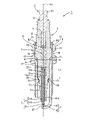
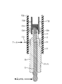
- FIG. 1 is a cross-sectional view of the spark plug 1 according to Embodiment 1 along the direction of the axis AX. 1 is the axis AX of the spark plug 1.
- the longitudinal direction of the spark plug 1 corresponds to the vertical direction in FIG.
- the lower side of FIG. 1 shows the front end side of the spark plug 1
- the upper side of FIG. 1 shows the rear end side of the spark plug 1.
- a spark plug 1 is attached to an automobile engine (an example of an internal combustion engine) and used to ignite an air-fuel mixture in a combustion chamber of the engine.
- a spark plug 1 mainly includes an insulator 2 , a center electrode 3 , a ground electrode 4 , a terminal fitting 5 , a metal shell 6 , a resistor 7 and sealing members 8 and 9 .
- the insulator 2 is a substantially cylindrical member extending in the direction of the axis AX and including a through hole 21 inside. Details of the insulator 2 will be described later.
- the metal shell 6 is a member used when the spark plug 1 is attached to an engine (specifically, an engine head). , low-carbon steel).
- a threaded portion 61 is formed on the outer peripheral surface of the metal shell 6 on the tip side.
- a ring-shaped gasket G is externally fitted to the rear end (so-called screw neck) of the threaded portion 61 .
- the gasket G is annular and formed by bending a metal plate. Such a gasket G is arranged between the rear end of the threaded portion 61 and the seat portion 62 arranged on the rear end side of the threaded portion 61, and when the spark plug 1 is attached to the engine, a spark is generated. It seals the gap formed between the plug 1 and the engine (engine head).
- a tool engaging portion 63 for engaging a tool such as a wrench when attaching the metal shell 6 to the engine is provided on the rear end side of the metal shell 6 .
- a thin crimped portion 64 bent radially inward is provided at the rear end portion of the metal shell 6 .
- the metal shell 6 also has a through hole 65 penetrating in the direction of the axis AX.
- the rear end of the insulator 2 protrudes greatly outward (upper side in FIG. 1) from the rear end of the metal shell 6 .
- the tip of the insulator 2 projects slightly outward (lower side in FIG. 1) from the tip of the metal shell 6 .
- An annular region is provided between the inner peripheral surface of the metal shell 6 from the tool engaging portion 63 to the crimping portion 64 and the outer peripheral surface of the insulator 2 (the outer peripheral surface of the rear cylindrical portion 25 described later). is formed, and the annular first ring member R1 and the annular second ring member R2 are arranged in the region in a state separated from each other in the direction of the axis AX.
- a powder of talc 10 is filled between the first ring member R1 and the second ring member R2.
- the rear end of the crimping portion 64 is bent radially inward and fixed to the outer peripheral surface of the insulator 2 (the outer peripheral surface of the rear cylindrical portion 25 described later).
- the metal shell 6 has a thin compression deformation portion 66 provided between the seat portion 62 and the tool engaging portion 63 .
- the compressively deformed portion 66 is compressively deformed when the caulking portion 64 fixed to the outer peripheral surface of the insulator 2 is pressed toward the distal end side during manufacture of the spark plug 1 .
- the insulator 2 is pressed forward within the metal shell 6 via the first ring member R1, the second ring member R2, and the talc 10 .
- the outer peripheral surface of the portion (the first expanded diameter portion 26 to be described later) that is a part of the insulator 2 and extends annularly is placed on the surface of the stepped portion 66 provided on the inner peripheral side of the metal shell 6.
- it is pressed while placing the packing P1 therebetween. Therefore, even if the gas in the combustion chamber of the engine enters the gap formed between the metal shell 6 and the insulator 2, the packing P1 provided in the gap prevents the gas from leaking to the outside. .
- the center electrode 3 is arranged inside the insulator 2 when the insulator 2 is mounted inside the metal shell 6 .
- the center electrode 3 includes a rod-shaped center electrode body 31 extending along the direction of the axis AX, and a substantially cylindrical (substantially disk-shaped) tip (center electrode tip) 32 attached to the tip of the center electrode body 31 .
- the center electrode main body 31 is a member whose length in the longitudinal direction is shorter than that of the insulator 2 and the metal shell 6, and is held in the through hole 21 of the insulator 2 so that the tip side thereof is exposed to the outside.
- the rear end of the center electrode main body 31 is accommodated inside the insulator 2 (through hole 21).
- the center electrode main body 31 includes an electrode base material 31A arranged outside and a core portion 31B embedded inside the electrode base material 31A.
- the electrode base material 31A is formed using, for example, nickel or an alloy containing nickel as a main component (eg, NCF600, NCF601).
- the core portion 31B is made of copper or a nickel-based alloy containing copper as a main component, which is superior in thermal conductivity to the alloy forming the electrode base material 31A.
- the center electrode body 31 includes an electrode collar portion 31a attached at a predetermined position in the direction of the axis AX, an electrode head portion 31b which is a portion on the rear end side of the electrode collar portion 31a, and and an electrode leg portion 31c, which is a portion on the tip side.
- the electrode collar portion 31 a is accommodated in the insulator 2 and supported by a stepped portion 23 a (described later) formed on the inner peripheral surface side of the insulator 2 .
- the tip of the electrode leg portion 31 c (that is, the tip of the center electrode main body 31 ) protrudes from the tip of the insulator 2 toward the tip side.
- the tip 32 has a substantially columnar shape (substantially disk shape) and is joined to the tip of the center electrode main body 31 (the tip of the electrode leg portion 31c) by resistance welding, laser welding, or the like.
- the tip 32 is made of a material whose main component is a noble metal with a high melting point (for example, an iridium-based alloy whose main component is iridium (Ir)).
- the terminal fitting 5 is a rod-shaped member extending in the direction of the axis AX, and is attached by being inserted into the rear end side of the through hole 21 of the insulator 2 .
- the terminal fitting 5 is arranged on the rear end side of the center electrode 3 in the insulator 2 (through hole 21 ).
- the terminal fitting 5 is made of a conductive metal material (for example, low carbon steel).
- the surface of the terminal fitting 5 may be plated with nickel or the like for the purpose of corrosion protection.
- the terminal fitting 5 includes a bar-shaped terminal leg portion 51 arranged on the front end side, a terminal flange portion 52 arranged on the rear end side of the terminal leg portion 51, and a terminal flange portion 52 arranged on the rear end side of the terminal flange portion 52.
- a cap mounting portion 53 is provided.
- the terminal leg portion 51 is inserted into the through hole 21 of the insulator 2 .
- the terminal collar portion 52 is a portion exposed from the rear end portion of the insulator 2 and engaged with the rear end portion.
- the cap attachment portion 53 is a portion to which a plug cap (not shown) to which a high-voltage cable is connected is attached, and a high voltage for generating spark discharge is applied from the outside via the cap attachment portion 53. .
- the resistor 7 is arranged in the through hole 21 of the insulator 2 between the front end of the terminal fitting 5 (the front end of the terminal leg portion 51) and the rear end of the center electrode 3 (the rear end of the center electrode main body 31). be.
- the resistor 7 has, for example, a resistance value of 1 k ⁇ or more (eg, 5 k ⁇ ), and has a function of reducing radio noise when sparks are generated.
- the resistor 7 is made of a composition containing glass particles as a main component, ceramic particles other than glass, and a conductive material.
- a gap is provided between the tip of the resistor 7 and the rear end of the center electrode 3 in the through hole 21, and the conductive sealing member 8 is arranged to fill the gap.
- a gap is also provided between the rear end of the resistor 7 and the tip of the terminal fitting 5 in the through hole 21, and the conductive sealing member 9 is arranged to fill the gap.
- Each of the sealing members 8 and 9 is made of a conductive composition containing, for example, B 2 O 3 —SiO 2 -based glass particles and metal particles (Cu, Fe, etc.).
- the ground electrode 4 comprises a ground electrode main body 41 joined to the tip of the metal shell 6 and a ground electrode tip 42 in the shape of a quadrangular prism.
- the ground electrode main body 41 is generally formed of a plate piece that is bent in a substantially L shape in the middle, and the rear end portion 41a thereof is joined to the front end of the metal shell 6 by resistance welding or the like. Thereby, the metal shell 6 and the ground electrode main body 41 are electrically connected.
- the ground electrode main body 41 is made of, for example, nickel or a nickel-based alloy containing nickel as a main component (for example, NCF600, NCF601), like the metal shell 6 .
- the ground electrode tip 42 is made of an iridium-based alloy containing iridium (Ir) as a main component.
- the ground electrode tip 42 is joined to the tip of the ground electrode main body 41 by laser welding.
- the ground electrode tip 42 at the tip of the ground electrode main body 41 and the tip 32 at the tip of the center electrode 3 are arranged to face each other while keeping a distance therebetween. That is, there is a gap SP between the tip 32 at the tip of the center electrode 3 and the ground electrode tip 42 at the tip of the ground electrode 4, and a high voltage is applied between the center electrode 3 and the ground electrode 4. is applied, a spark discharge is generated in the gap SP along the direction of the axis AX.
- the insulator 2 generally has a tubular shape (cylindrical shape) elongated along the direction of the axis AX, and as shown in FIG. contains.
- the insulator 2 is composed of a tubular (cylindrical) alumina-based sintered body containing alumina as a main component.
- the insulator 2 includes a long leg portion 22 disposed on the distal end side, a middle body portion 23 disposed on the rear end side of the long leg portion 22 and having a larger diameter than the long leg portion 22, and a middle body portion 23.
- a collar portion 24 which is arranged on the rear end side of the body and has a diameter larger than that of the middle body portion 23 .
- a first enlarged diameter portion 26 is provided between the long leg portion 22 and the middle body portion 23, and a second enlarged diameter portion 27 is provided between the middle body portion 23 and the collar portion 24. is provided.
- the long leg portion 22 has an overall elongated tube shape (cylindrical shape) whose outer diameter gradually increases from the front side to the rear side, and is larger than the middle body portion 23 and the first enlarged diameter portion 26 . It has a small outer diameter.
- the long leg portion 22 is exposed to the combustion chamber when the spark plug 1 is attached to the engine (engine head).
- the flange portion 24 is arranged substantially in the center of the insulator 2 in the direction of the axis AX and has an annular shape.
- a resistor 7 is arranged in the through hole 21 inside the collar portion 24 .
- the first enlarged diameter portion 26 is a portion that connects the long leg portion 22 and the middle body portion 23, and has a cylindrical shape (annular shape) whose outer diameter gradually increases from the front side to the rear side.
- the second enlarged diameter portion 27 is a portion that connects the middle body portion 23 and the collar portion 24, has an outer diameter larger than that of the first enlarged diameter portion 26, and gradually increases in diameter from the front side to the rear side. It has a cylindrical (annular) shape that grows larger.
- the middle body part 23 has a tubular shape (cylindrical shape) with an approximately uniform outer diameter in the direction of the axis AX.
- FIG. 1 shows a range L1 occupied by the middle body portion 23 in the direction of the axis AX.
- the electrode collar portion 31a of the center electrode main body 31 is supported by the surface of the stepped portion 23a.
- the thickness of the wall portion of the middle body portion 23 is greater than the thickness of the wall portion of the long leg portion 22 .
- the wall thickness of the portion of the middle body portion 23 where the stepped portion 23a is formed from the front end side is greater than the thickness of the wall portion of the portion behind the stepped portion 23a.
- the outer peripheral surface of the middle body part 23 is exposed to the atmosphere (air), and it can be said that it is in an environment where electricity can easily pass through compared to the long leg part 22 . Therefore, the middle body portion 23 is set to have a larger wall thickness than the long leg portion 22 .
- the “thickness of the middle body portion 23” means a portion of the middle body portion 23 where the thickness of the wall portion is substantially constant (that is, the rear end side of the stepped portion 23a). part) is the thickness of the wall.
- the thickness of the middle body portion 23 is not particularly limited as long as it does not impair the purpose of the present invention. The technical effects of the present invention are exhibited more remarkably when the thickness of the middle body portion 23 is 2.0 mm or less.
- the insulator 2 further includes a tubular (cylindrical) rear tubular portion 25 connected to the rear end side of the flange portion 24 and extending in the direction of the axis AX.
- the rear tubular portion 25 has an outer diameter smaller than the outer diameter of the collar portion 24 .
- a rod-shaped terminal leg portion 51 and the like of the terminal fitting 5 are arranged in the through hole 21 inside the rear cylindrical portion 25 .
- the middle body part 23 is the part of the insulator 2 that is most likely to be affected by the reduction in diameter, and dielectric breakdown is more likely to occur as the diameter is reduced. Therefore, if the middle body portion 23 has an internal structure containing pores that satisfies at least all of the following conditions 1 and 2, the insulator 2 (spark plug 1) having excellent withstand voltage performance can be obtained. can get.
- a cut surface obtained by cutting the middle trunk portion 23 in a direction perpendicular to the direction of the axis line AX at an arbitrary position in the direction of the axis line AX (that is, a cut surface obtained by cutting the middle trunk portion 23 into a ring shape)
- 20 observation areas of 185 ⁇ m ⁇ 250 ⁇ m (rectangular observation areas of 185 ⁇ m in length and 250 ⁇ m in width) were set so as not to overlap each other, and these 20 observation areas
- the square value P 2 [ ⁇ m 2 ] of the perimeter length P [ ⁇ m] of each pore is obtained for each of the included pores, the top 20 with the largest square value P 2 [ ⁇ m 2 ]
- the pores are included in the middle body portion 23 of the insulator 2 so that the average value of the square value P 2 [ ⁇ m 2 ] of the pores is 2200 ⁇ m 2 or less.
- the ratio T [%] of the total area of all pores included in the 20 observation regions to the total area (100%) of the 20 observation regions is 5% or less.
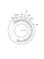
- FIG. 2 is an explanatory diagram schematically showing a cut surface 23b of the middle body portion 23.
- the middle body portion 23 is cut at an arbitrary position in the direction of the axis AX in a direction perpendicular to the direction of the axis AX, and after cutting, the mirror-polished surface is mirror-polished. Face 23b is shown.
- the mirror-polished surface of the cut surface 23b may be referred to as "mirror-polished surface 23b" using the same reference numeral as the cut surface 23b.
- the mirror-polishing treatment of the cut surface 23b is performed based on a known method using a diamond whetstone, diamond paste, or the like.
- the mirror polishing process is performed until the surface roughness (Ra) of the cut surface 23b reaches, for example, about 0.001 ⁇ m.
- the mirror-polished surface 23b of the middle body portion 23 is observed using a scanning electron microscope (SEM). Therefore, the mirror-polished surface 23b may be subjected to carbon vapor deposition for imparting conductivity, if necessary.
- the acceleration voltage of the SEM is set to 20 kV, for example, and the magnification of the SEM is set to 500 times, for example.
- the mirror-polished surface 23b has an annular shape, and on the annular mirror-polished surface 23b, observation areas X each having a size of 185 ⁇ m ⁇ 250 ⁇ m are arranged in a ring so as not to overlap each other. 20 are set so as to be lined up.
- Each observation region X is acquired as an SEM image of a predetermined location on the mirror-polished surface 23b using an SEM.
- a plurality of observation regions X are schematically shown in FIG.
- a subscript (a number from 1 to 20) is attached to each symbol X in order to distinguish the observation regions X from each other.
- the observation area X1 is the observation area X set first
- the observation area X20 is the observation area X set twentieth.
- a total of 20 SEM images corresponding to a total of 20 observation regions X set in this way are analyzed using known image analysis software (for example, WinROOF (registered trademark)) executed on a computer. Analysis processing (two-dimensional image analysis processing) is performed.
- image analysis software for example, WinROOF (registered trademark)
- Analysis processing two-dimensional image analysis processing
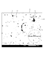
- FIG. 3 is an explanatory diagram showing a binarized image obtained by binarizing the SEM image corresponding to the observation region X.
- a binarized image can be obtained by converting the image into two gradations and eliminating intermediate gradations.
- the pores 11 are shown in black, and the other portion (ceramic portion) 12 is shown in white.
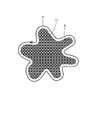
- FIG. 4 is an explanatory diagram schematically showing one arbitrarily selected pore 11 out of all the pores. Further, for each of the extracted pores, the square value P 2 [ ⁇ m 2 ] of the measured perimeter length P [ ⁇ m] of the pores is calculated. The square value P 2 [ ⁇ m 2 ] is obtained for all the pores 11 included in the 20 observation regions X, respectively.
- the top 20 pores 11 having the largest square value P 2 [ ⁇ m 2 ] are selected. is elected. Then, the average value of the square values P 2 [ ⁇ m 2 ] of the top 20 pores is calculated. In the case of this embodiment, the average value of the square value P 2 [ ⁇ m 2 ] is set to 2200 ⁇ m 2 or less.
- the contour shape of the pores included in the middle body portion 23 is more perfect circle on the cut surface (mirror-polished surface) 23b. It means that the smaller the size of the pores included in the middle body portion 23 is, the better.
- the technical significance of the pore squared value P 2 [ ⁇ m 2 ] will be further described.
- an arbitrary one pore extracted from the binarized image will be described as an example.
- the contour shape of the pores can be evaluated using the unevenness of the pores as an index.
- the unevenness of pores is expressed by (P 2 /A) ⁇ (1/4 ⁇ ).
- P represents the outer circumference of the pore P [ ⁇ m]
- A represents the area of the pore [ ⁇ m 2 ].
- the size of the pores can be evaluated by the area A [ ⁇ m 2 ] of the pores.
- the index V for collectively evaluating the “contour shape” and “size” of one pore, the unevenness of the pore ((P 2 /A) ⁇ (1/4 ⁇ )) and the area A of the pore It is empirically known that the product of [ ⁇ m 2 ] ((P 2 /A) ⁇ (1/4 ⁇ ) ⁇ A) can be used. In this case, it is clear that the index V is proportional to the square value P 2 [ ⁇ m 2 ]. As an index, the square value P 2 [ ⁇ m 2 ] of the length P [ ⁇ m] of the perimeter of the pore was used.
- the area A [ ⁇ m 2 ] is also measured.
- the measured area A [ ⁇ m 2 ] of each pore is used in the definition of condition 2 described later.
- the ratio of the total area of all pores included in all observation regions X to the area of all observation regions X (total area of 20 observation regions X) (100%)
- the pores 11 in the internal structure of the middle body portion 23 of the insulator 2 are adjusted so that the ratio T [%] is 5% or less.
- the total area of all pores under Condition 2 is the sum of the pore areas A [ ⁇ m 2 ] measured for all pores.
- the area A [ ⁇ m 2 ] of one pore is preferably adjusted to 5,000 ⁇ m 2 or less.
- a circle having an area of approximately 5,000 ⁇ m 2 is shown in the binarized image of FIG. 3 for comparison with the size of the pores 11 .
- the internal structure of the middle body portion 23 may be adjusted so as to satisfy the following conditions other than conditions 1 and 2 above. Specifically, for each of the 20 observation regions X, the pore area distribution is approximated by a logarithmic normal distribution, and when the cumulative 50% area of the cumulative distribution in the pore area is obtained, the cumulative 50% The area may be greater than 3 ⁇ m 2 . If the middle body portion 23 satisfies such conditions, the insulator 2 with excellent impact resistance can be obtained.
- the internal structure of the mid-torso 23 may be adjusted so as to satisfy the conditions shown below. Specifically, the ratio T [%] shown in Condition 2 above may be 3% or less.
- the insulator 2 is manufactured so as to satisfy the conditions 1 and 2 described above.
- the method for manufacturing the insulator 2 is not particularly limited as long as the finally obtained insulator 2 satisfies the conditions 1, 2 and the like.
- an example of a method for manufacturing the insulator 2 will be described.
- the method of manufacturing the insulator 2 mainly includes a slurry preparation process, a defoaming process, a granulation process, a sieving process, a molding process, a grinding process, and a firing process.
- a slurry preparation process is a process of mixing raw material powder, a binder, and a solvent to prepare a slurry.
- the raw material powder powder of a compound that is converted into alumina by firing (hereinafter referred to as Al compound powder) is used as a main component.
- Al compound powder powder of a compound that is converted into alumina by firing
- alumina powder is used as the Al compound powder.
- the particle size (median size) of the Al compound powder is not particularly limited as long as it does not impair the purpose of the present invention, but is, for example, 1.5 ⁇ m to 2.5 ⁇ m.
- the particle size is a volume-based median diameter (D50) measured by a laser diffraction method (manufactured by Nikkiso Co., Ltd., Microtrac particle size distribution analyzer, product name “MT-3000”).
- the Al compound powder is preferably prepared so that the mass of the alumina-based sintered body after sintering (calculated as oxide) is 100% by mass, and is 90% by mass or more in terms of oxide.
- the raw material powder may contain powder other than the Al compound powder as long as the object of the present invention is not impaired.
- the binder is added to the slurry for the purpose of improving the moldability of the raw material powder.
- binders include hydrophilic binders such as polyvinyl alcohol, aqueous acrylic resins, gum arabic and dextrin. You may use these individually or in combination of 2 or more types.
- the amount of the binder to be blended is not particularly limited as long as it does not impair the purpose of the present invention. It is blended at a ratio of 0.3 parts by mass to 0.9 parts by mass.
- the solvent is used for purposes such as dispersing the raw material powder.
- solvents include water and alcohols. You may use these individually or in combination of 2 or more types.
- the amount of the solvent to be blended is not particularly limited as long as it does not impair the object of the present invention. It is blended at a ratio of 42 parts by mass.
- the slurry may optionally contain other components than the raw material powder, binder and solvent.
- a known stirring/mixing device or the like can be used for mixing the slurry.
- the slurry after the slurry production process may be subjected to a defoaming process.
- the defoaming step for example, the container containing the slurry after mixing (kneading) is placed in a vacuum defoaming device and placed in a low-pressure environment to decompress the air bubbles contained in the slurry. removed.
- the amount of air bubbles in the slurry can be grasped.
- the granulation step is a step of producing spherical granulated powder from a slurry containing raw material powder and the like.
- the method for producing the granulated powder from the slurry is not particularly limited as long as it does not impair the object of the present invention, and examples thereof include spray drying.
- a granulated powder having a predetermined particle size is obtained by spray-drying the slurry using a predetermined spray dryer.
- the sieving step is a step of removing foreign matter and the like contained in the granulated powder by passing the granulated powder through a sieve having a predetermined mesh size.
- the mesh size of the sieve used in the sieving step is set to be, for example, 150% to 300% of the average particle size of the granulated powder. More specifically, the mesh size of the sieve is adjusted, for example, within the range of 150 ⁇ m or more and 350 ⁇ m or less.
- the molding step is a step of molding the granulated powder into a predetermined shape using a molding die to obtain a molded body.
- the molding process is performed by rubber press molding, die press molding, or the like.
- the pressure applied from the outer peripheral side to the mold (for example, the inner rubber mold and the outer rubber mold of a rubber press molding machine) (press pressure increase speed) is adjusted to increase stepwise.
- the pressure is less than half the maximum press pressure during the molding press, by providing a stop time of 0.2 seconds or more for increasing the pressure, the granules will not be crushed and the size and shape of the pores will be controlled. can be done.
- stopping the pressure increase refers to the case where the increase/decrease value of the press pressure is 1/20 or less of the maximum press pressure.
- the grinding step is a step of removing machining allowance from the molded body obtained after the molding step and polishing the surface of the molded body.
- machining allowance is removed and the surface of the compact is polished by grinding with a resinoid grindstone or the like. Through such a grinding process, the shape of the compact is adjusted.
- the sintering step is a step of sintering the compact shaped by the grinding step to obtain an insulator.
- firing step for example, firing is performed at 1450° C. or higher and 1650° C. or lower in an air atmosphere for 1 to 8 hours.
- the molded body is cooled to obtain the insulator 2 made of an alumina-based sintered body.
- the spark plug 1 of this embodiment is manufactured using the insulator 2 obtained as described above.
- the structure of the spark plug 1 other than the insulator 2 is the same as the known structure as described above.
- test samples Insulators (hereinafter referred to as test samples) having the same basic configuration as the spark plug insulators exemplified in Embodiment 1 were produced by the same manufacturing method as in Embodiment 1 (a total of 41 insulators). .
- the middle body of the test sample is cylindrical and its thickness is 2.0 mm.
- FIG. 5 is an explanatory diagram schematically showing a method of measuring the penetration voltage of the test sample T1 by an underwater withstand voltage test.
- a pre-test preparation for the test sample T1 spark plug insulator 2
- a first silicone tube T30 is attached to the tip portion 22a of the insulator 2, and in that state, the tip portion Silicone rubber T31 was injected into the through hole 21 in 22a for the purpose of insulation and solidified.
- the length of the center electrode 3 is previously adjusted by cutting or the like so as not to come into contact with the solidified silicone rubber T31.
- a second silicone tube T32 having an inner diameter larger than that of the first silicone tube T30 is prepared.
- a second silicone tube T32 was attached to the collar portion 24 of the insulator 2 .
- a gap T33 formed between the second silicone tube T32 and the first silicone tube T30 was soaked with a saline solution (concentration: 1% by mass) T34.
- the center electrode 3 and the terminal fitting 5 were inserted from the rear end side of the rear cylindrical portion 25 into the through hole 21 inside.
- test needle T35 is inserted into the second silicone tube T32 so that it is positioned substantially in the center of the middle body portion 23 in the axial direction of the test sample T1 (insulator 2) and the tip thereof is in contact with the saline solution T34. installed.
- the test needle T35 attached in this manner was used as the ground side, and a high voltage was applied to the terminal fitting 5 exposed from the rear end of the test sample T1 (insulator 2) under the conditions described later. Specifically, while watching the oscilloscope, the voltage was increased from the starting voltage (20 kV) to 30 kV at 1 kV/sec. The voltage was increased by 1 kV from the starting voltage, each voltage was held for 10 seconds, and the voltage that penetrated was recorded.
- test spark plugs (hereinafter referred to as test spark plugs) having the same configuration as that exemplified in the first embodiment were produced. With the axial direction of the test spark plug set in the vertical direction and the tip side directed downward, the threaded portion of the metal shell of the test spark plug was screwed into a screw hole provided in the test stand and fixed. Also, a hammer having a pivot point above the fixed test spark plug in the axial direction was rotatably provided.
- the middle body part of the obtained test sample was cut perpendicularly to the axial direction, and the obtained cut surface was mirror-polished, and then the structure of the cut surface (mirror-polished surface) was observed with an SEM. .
- the acceleration voltage of the SEM was set to 20 kV, and the magnification of the SEM was set to 500 times.
- 20 observation regions (185 ⁇ m ⁇ 250 ⁇ m) were set on the cut surface (mirror-polished surface) so as not to overlap each other, and a total of 20 SEM images corresponding to these 20 observation regions were acquired.
- the SEM images are subjected to image analysis processing using image analysis software (WinROOF (registered trademark)), and the length of the outer circumference of each of the pores included in the 20 observation regions is determined. P [ ⁇ m] and square value P 2 [ ⁇ m] were obtained. Then, 20 pores having the largest square value P 2 [ ⁇ m] were selected from the plurality of pores, and the average value of the square value P 2 [ ⁇ m] of the selected 20 pores was calculated. The results are shown in Table 1.
- WinROOF registered trademark
- Example 2 to 9 Test samples of Examples 2 to 9 were produced in the same manner as in Example 1, except that the pressing pressure during the pressure increase stop time was appropriately changed during the molding press in the molding process.
- Example 10 In the same manner as in Example 1, except that the thickness of the middle body portion was changed to 3.0 mm, and the press pressure during the pressure increase stop time was changed during the molding press in the molding process. A test sample was made.
- Comparative Examples 1 and 2 Test samples of Comparative Examples 1 and 2 were produced in the same manner as in Example 1, except that no pressure increase stop time was provided during the molding press in the molding process.
- Comparative Example 3 A test sample of Comparative Example 3 was prepared in the same manner as in Example 1, except that the thickness of the middle body portion was changed to 3.0 mm and the pressure increase stop time was not provided during the molding press in the molding process. made.
- Example 1 As in Example 1, the above “measurement of underwater withstand voltage”, “evaluation of impact resistance”, and “observation of cut surface” were performed on the obtained test sample. Those results are shown in Table 1. For Example 10 and Comparative Example 3, the impact resistance was not evaluated.
- the 20 pores with the largest square value P 2 [ ⁇ m 2 ] are The average values of the multiplied values P 2 [ ⁇ m 2 ] are all 2200 ⁇ m 2 or less, indicating excellent withstand voltage performance.
- the ratio T [%] of the total area of all pores included in the 20 observation regions to the total area (100%) of the 20 observation regions was 5.0. % or less.
- no pores having an area exceeding 5,000 ⁇ m were found.
- Example 10 in which the thickness of the middle body portion was 3 mm, was superior in withstand voltage performance compared to Comparative Example 3, in which the thickness of the middle body portion was also 3 mm.
- Examples 1 to 9 are cases where the cumulative 50% area in the cumulative distribution of the pore area exceeds 3 ⁇ m 2 , and each such implementation It was confirmed that the examples are superior in impact resistance as compared with Examples 5 to 7 in which the cumulative 50% area is 3 ⁇ m 2 or less.
- Example 1 in which the thickness of the mid-torso is 2 mm and the average value of the square value P 2 [ ⁇ m 2 ] is 1470 ⁇ m 2 , and the average value of the square value P 2 [ ⁇ m 2 ] is 7820 ⁇ m 2 When compared with Comparative Example 1, the difference in underwater withstand voltage was 8 kV/mm.
- Example 10 in which the thickness of the mid-torso is 3 mm and the average value of the squared values P 2 [ ⁇ m 2 ] is 1465 ⁇ m 2 and the average of the squared values P 2 [ ⁇ m 2 ] When compared with Comparative Example 3 with a value of 7820 ⁇ m 2 , the difference in underwater withstand voltage was 5 kV/mm. As described above, it was confirmed that even if the square value P 2 [ ⁇ m 2 ] is approximately the same, the withstand voltage performance is greatly improved as the thickness of the middle body portion is decreased.
Landscapes
- Engineering & Computer Science (AREA)
- Manufacturing & Machinery (AREA)
- Spark Plugs (AREA)
Abstract
Description
筒状をなした絶縁体の壁部内には、通常、細かな気孔(空隙)がある程度、存在している。この種の気孔は、絶縁体の製造過程において、不可避的に形成されるものであり、極端に大きな気孔(例えば、直径が5,000μmを超える気孔)が形成された場合以外は、通常、その存在が問題視されることは少ない。しかしながら、絶縁体の小径化に伴って、絶縁体の壁部の厚みが小さくなると、気孔の存在を無視できなくなり、気孔が絶縁体の耐電圧性能の低下に影響を及ぼす場合があった。
本発明者等は、アルミナ基焼結体からなる絶縁体を備えたスパークプラグにおいて、その絶縁体の中胴部の内部に、ある一定以上の大きさを備えつつ、表面が凹凸状の気孔(空隙)が存在していると、スパークプラグの使用時に、その気孔を取り囲む凹凸状の輪郭部分に、局所的な電界集中が発生して、絶縁体の破壊が引き起こされることをつきとめた。
<1> 軸線方向に沿って延びた筒状をなし、先端側に配される脚長部と、前記脚長部の後端側に配され前記脚長部よりも大径である中胴部と、前記中胴部の後端側に配され前記中胴部よりも大径である鍔部とを有し、アルミナ基焼結体からなる絶縁体を備えるスパークプラグであって、前記中胴部を、前記軸線方向における任意の位置で、前記軸線方向に対して垂直な方向に切断することで得られる切断面を、鏡面研磨した鏡面研磨面において、互いに重ならないように185μm×250μmの観察領域を20個設定すると共に、前記20個の観察領域に含まれる複数の気孔について、それぞれ、気孔の外周の長さP[μm]の2乗値P2[μm2]を求めた場合に、その2乗値P2[μm2]の大きい上位20個の気孔における2乗値P2[μm2]の平均値が2200μm2以下であり、かつ前記20個の観察領域の前記合計面積(100%)に対する、前記20個の観察領域に含まれる全ての気孔の合計面積の割合T[%]が5%以下であるスパークプラグ。
本発明によれば、耐電圧性能に優れる絶縁体を備えたスパークプラグを提供することができる。
本発明の実施形態1に係るスパークプラグ1を、図1~図4を参照しつつ説明する。図1は、実施形態1に係るスパークプラグ1の軸線AX方向に沿った断面図である。図1に示される上下方向に延びた一点鎖線は、スパークプラグ1の軸線AXであり、図1において、スパークプラグ1の長手方向(軸線AX方向)が、図1の上下方向に対応する。図1の下側に、スパークプラグ1の先端側が示され、図1の上側に、スパークプラグ1の後端側が示される。
中胴部23を、軸線AX方向における任意の位置で、軸線AX方向に対して垂直な方向に切断することで得られる切断面(つまり、中胴部23を輪切り状にして得られる切断面)23bを鏡面研磨した鏡面研磨面において、互いに重ならないように185μm×250μmの観察領域(縦:185μm、横:250μmの矩形状の観察領域)を20個設定すると共に、それら20個の観察領域に含まれる複数の気孔について、それぞれ、気孔の外周の長さP[μm]の2乗値P2[μm2]を求めた場合に、その2乗値P2[μm2]の大きい上位20個の気孔における2乗値P2[μm2]の平均値が2200μm2以下となるように、気孔が絶縁体2の中胴部23に含まれている。
全ての気孔において、前記20個の観察領域の合計面積(100%)に対する、前記20個の観察領域に含まれる全ての気孔の合計面積の割合T[%]は、5%以下である。
スラリー作製工程は、原料粉末、バインダー及び溶媒を混合してスラリーを作製する工程である。原料粉末は、主成分として、焼成によりアルミナに転化する化合物の粉末(以下、Al化合物粉末)が使用される。Al化合物粉末としては、例えば、アルミナ粉末が使用される。
スラリー作製工程後のスラリーに対して、必要に応じて、脱泡工程を行ってもよい。脱泡工程では、例えば、混合(混錬)後のスラリーの入った容器を、真空脱泡装置内に配置して、減圧して低気圧環境下に置くことで、スラリー内に含まれる気泡が取り除かれる。脱泡前後のスラリーの密度を比較することで、スラリー中の気泡量を把握することができる。
造粒工程は、原料粉末等を含むスラリーから、球状の造粒粉を作製する工程である。スラリーから造粒粉を作製する方法としては、本発明の目的を損なわない限り特に制限はないが、例えば、スプレードライ法が挙げられる。スプレードライ法では、所定のスプレードライヤー装置を利用して、スラリーを噴霧乾燥することにより、所定の粒径を備えた造粒粉が得られる。
通篩工程は、造粒粉を、所定の目開きを有する篩を通過させることで、造粒粉中に含まれる異物等を除去する工程である。通篩工程で使用される篩の目開きは、例えば、造粒粉の平均粒径に対して、150%~300%の大きさとなるように設定される。より具体的には、篩の目開きは、例えば150μm以上350μm以下の範囲に調整される。
成形工程は、造粒粉を、成形型を利用して所定形状に成形することで成形体を得る工程である。成形工程は、ラバープレス成形や金型プレス成形等によって行われる。本実施形態の場合、成形型(例えば、ラバープレス成形機の内ゴム型及び外ゴム型)を外周側から印加する圧力(プレス昇圧速度)は、段階的に上昇するように調整される。なお、成形プレスの際に、最高プレス圧の半分以下の圧力の時に0.2秒以上の増圧の停止時間を設けることで、顆粒のつぶれ残りがなくなり、気孔の大きさと形を制御することができる。最高プレス圧の半分より大きいプレス圧の時に増圧の停止時間を設けると、成形体に過剰な圧力がかかり、成形体にキレ(切れ目)等の欠陥が発生する。なお、「増圧の停止」とは、プレス圧の増加・減少の値が、最高プレス圧の1/20以下の場合をいう。
研削工程は、成形工程後に得られた成形体の加工取り代の除去や成形体の表面を研磨等する工程である。研削工程では、レジノイド砥石等を研削することにより、加工取り代の除去や成形体の表面の研磨等が行われる。このような研削工程により、成形体の形状が整えられる。
焼成工程は、研削工程により形状が整えられた成形体を焼成して、絶縁体を得る工程である。焼成工程では、例えば、大気雰囲気下で、1450℃以上1650℃以下で1~8時間焼成する。焼成後、成形体を冷却することにより、アルミナ基焼結体からなる絶縁体2が得られる。
(試験サンプルの作製)
上記実施形態1で例示したスパークプラグの絶縁体と、基本的な構成が同じである絶縁体(以下、試験サンプル)を、上記実施形態1と同様の製造方法で作製(合計41本作製)した。試験サンプルの中胴部は、円筒状であり、その厚みは、2.0mmである。
以下に示される水中耐電圧試験を行い、貫通電圧の測定を行った。具体的な内容は以下の通りである。図5は、水中耐電圧試験により試験サンプルT1の貫通電圧を測定する方法を模式的に表した説明図である。図5に示されるように、先ず、試験サンプルT1(スパークプラグの絶縁体2)に対する試験前準備として、絶縁体2の先端部22aに第1シリコーンチューブT30を装着し、その状態で、先端部22a内の貫通孔21に、絶縁を目的としてシリコーンゴムT31を注入して固化させた。なお、中心電極3は、固化したシリコーンゴムT31と接触しないように、予めその長さが、切断等によって調整されている。次いで、第1シリコーンチューブT30よりも、内径が大きい第2シリコーンチューブT32を用意し、その第2シリコーンチューブT32の内側に、第1シリコーンチューブT30を装着した先端部22aが配置されるように、第2シリコーンチューブT32を、絶縁体2の鍔部24に装着した。そして、第2シリコーンチューブT32と、第1シリコーンチューブT30との間に形成される隙間T33を、食塩水(濃度:1質量%)T34で浸した。また、後側筒部25の後端側から、内部の貫通孔21に対して、図5に示されるように、中心電極3及び端子金具5を挿し込む形で装着した。そして、試験サンプルT1(絶縁体2)の軸線方向において、中胴部23の略中央の位置おなり、かつ先端が食塩水T34に接触するように、第2シリコーンチューブT32に、試験針T35を取り付けた。このように取り付けた試験針T35をアース側とし、試験サンプルT1(絶縁体2)の後端から露出した端子金具5に、後述する条件で、高電圧を印加した。具体的には、オシリスコープを見ながら、開始電圧(20kV)から30kVまで、1kV/secで昇圧した。開始電圧から1kVずつ昇圧させ、各電圧で10秒間保持し、貫通した電圧を記録した。なお、水中耐電圧試験の際、高電圧側の配線は、なるべく空気中に配置し、絶縁物上には必要最小限の部分を載置した。また、中心電極3及び端子金具5は、すべての試験サンプルT1の試験について、同じものを使用した。このような作業を、20本の試験サンプル(絶縁体)に対して行った。試験結果は、20本の試験サンプルについての平均値とした。結果は、表1に示した。
各試験サンプルに対して、JIS B7733に規定されるシャルピー試験を行い、試験サンプル(絶縁体)が破断する破断エネルギーの測定を行った。具体的な内容は、以下の通りである。先ず、試験サンプルである絶縁体を使用して、上記実施形態1で例示したものと同様の構成のスパークプラグ(以下、試験用スパークプラグ)を作製した。その試験用スパークプラグの軸線方向を上下方向として、先端側を下方に向け、試験台に設けられたネジ孔に試験用スパークプラグの主体金具のネジ部を螺合させて固定した。また、固定した試験用スパークプラグの軸線方向の上方に軸支点を有するハンマーを旋回可能に設けた。そして、ハンマーの先端を持ち上げてリリースし、自由落下によりハンマーを旋回させ、ハンマーの先端を絶縁体の後端より略1mmの部位に衝突させた。このハンマーの持ち上げ角度(軸線方向に対する角度)を、所定角度ずつ大きくしながらハンマーの先端を試験用スパークプラグの絶縁体に衝突させた。このような操作を繰り返し、絶縁体に破断が生じた際の持ち上げ角度に基づいて絶縁体のシャルピー破断エネルギー[J]を求めた。このような作業を、20本の試験サンプル(絶縁体)に対して行った。試験結果は、20本の試験サンプルについての平均値とした。結果は、表1に示した。
得られた試験サンプルの中胴部を、軸線方向に対して垂直に切断し、得られた切断面を、鏡面状に研磨した後、その切断面(鏡面研磨面)の組織をSEMで観察した。SEMの加速電圧は、20kVに設定し、SEMの倍率は、500倍に設定した。そして、その切断面(鏡面研磨面)において、互いに重ならないように観察領域(185μm×250μm)を20個設定し、それら20個の観察領域に対応した合計20個のSEM画像を取得した。そして、それらのSEM画像に対して、画像解析ソフト(WinROOF(登録商標))による画像解析処理を実行して、20個の観察領域に含まれる複数の気孔について、それぞれ、気孔の外周の長さP[μm]、及び2乗値P2〔μm〕を求めた。そして、複数の気孔の中から、2乗値P2〔μm〕の大きい上位20個の気孔を選出し、選出した20個の気孔の2乗値P2〔μm〕の平均値を算出した。結果は、表1に示した。
成形工程における成形プレスの際に、増圧の停止時間におけるプレス圧を適宜、変更したこと以外は、実施例1と同様にして、実施例2~9の試験サンプルを作製した。
中胴部の厚みを3.0mmに変更すると共に、成形工程における成形プレスの際に、増圧の停止時間におけるプレス圧を変更したこと以外は、実施例1と同様にして、実施例10の試験サンプルを作製した。
成形工程における成形プレスの際に、増圧の停止時間を設けないこと以外は、実施例1と同様にして、比較例1,2の試験サンプルを作製した。
中胴部の厚みを3.0mmに変更すると共に、成形工程における成形プレスの際に、増圧の停止時間を設けないこと以外は、実施例1と同様にして、比較例3の試験サンプルを作製した。

Claims (4)
- 軸線方向に沿って延びた筒状をなし、先端側に配される脚長部と、前記脚長部の後端側に配され前記脚長部よりも大径である中胴部と、前記中胴部の後端側に配され前記中胴部よりも大径である鍔部とを有し、アルミナ基焼結体からなる絶縁体を備えるスパークプラグであって、
前記中胴部を、前記軸線方向における任意の位置で、前記軸線方向に対して垂直な方向に切断することで得られる切断面を、鏡面研磨した鏡面研磨面において、互いに重ならないように185μm×250μmの観察領域を20個設定すると共に、前記20個の観察領域に含まれる複数の気孔について、それぞれ、気孔の外周の長さP[μm]の2乗値P2[μm2]を求めた場合に、その2乗値P2[μm2]の大きい上位20個の気孔における2乗値P2[μm2]の平均値が2200μm2以下であり、かつ
前記20個の観察領域の前記合計面積(100%)に対する、前記20個の観察領域に含まれる全ての気孔の合計面積の割合T[%]が5%以下であるスパークプラグ。 - 前記20個の観察領域それぞれについての、前記気孔の面積の累積分布における累積50%の面積が、3μm2を超える値である請求項1に記載のスパークプラグ。
- 前記割合Tが3%以下である請求項1又は請求項2に記載のスパークプラグ。
- 前記中胴部の厚みが、2.0mm以下である請求項1から請求項3の何れか一項に記載のスパークプラグ。
Priority Applications (3)
| Application Number | Priority Date | Filing Date | Title |
|---|---|---|---|
| US18/567,550 US12095234B2 (en) | 2021-06-14 | 2022-06-14 | Spark plug |
| DE112022003101.8T DE112022003101T5 (de) | 2021-06-14 | 2022-06-14 | Zündkerze |
| CN202280041637.8A CN117461227A (zh) | 2021-06-14 | 2022-06-14 | 火花塞 |
Applications Claiming Priority (2)
| Application Number | Priority Date | Filing Date | Title |
|---|---|---|---|
| JP2021098895A JP7305707B2 (ja) | 2021-06-14 | 2021-06-14 | スパークプラグ |
| JP2021-098895 | 2021-06-14 |
Publications (1)
| Publication Number | Publication Date |
|---|---|
| WO2022264996A1 true WO2022264996A1 (ja) | 2022-12-22 |
Family
ID=84526476
Family Applications (1)
| Application Number | Title | Priority Date | Filing Date |
|---|---|---|---|
| PCT/JP2022/023731 Ceased WO2022264996A1 (ja) | 2021-06-14 | 2022-06-14 | スパークプラグ |
Country Status (5)
| Country | Link |
|---|---|
| US (1) | US12095234B2 (ja) |
| JP (1) | JP7305707B2 (ja) |
| CN (1) | CN117461227A (ja) |
| DE (1) | DE112022003101T5 (ja) |
| WO (1) | WO2022264996A1 (ja) |
Families Citing this family (1)
| Publication number | Priority date | Publication date | Assignee | Title |
|---|---|---|---|---|
| JP2024141053A (ja) * | 2023-03-29 | 2024-10-10 | 日本特殊陶業株式会社 | スパークプラグ |
Citations (2)
| Publication number | Priority date | Publication date | Assignee | Title |
|---|---|---|---|---|
| JP2007250379A (ja) * | 2006-03-16 | 2007-09-27 | Ngk Spark Plug Co Ltd | 内燃機関用スパークプラグ及びその製造方法 |
| JP2015069828A (ja) * | 2013-09-30 | 2015-04-13 | 日本特殊陶業株式会社 | 点火プラグ |
Family Cites Families (3)
| Publication number | Priority date | Publication date | Assignee | Title |
|---|---|---|---|---|
| DE102018101512B4 (de) * | 2018-01-24 | 2020-03-19 | Federal-Mogul Ignition Gmbh | Verfahren zum Herstellen einer Elektrodenanordnung, Elektrodenanordnung und Zündkerze |
| JP7077189B2 (ja) * | 2018-09-07 | 2022-05-30 | 田中貴金属工業株式会社 | スパークプラグ電極用材料及びその製造方法 |
| JP6843809B2 (ja) | 2018-10-03 | 2021-03-17 | 日本特殊陶業株式会社 | スパークプラグ |
-
2021
- 2021-06-14 JP JP2021098895A patent/JP7305707B2/ja active Active
-
2022
- 2022-06-14 US US18/567,550 patent/US12095234B2/en active Active
- 2022-06-14 CN CN202280041637.8A patent/CN117461227A/zh active Pending
- 2022-06-14 DE DE112022003101.8T patent/DE112022003101T5/de active Pending
- 2022-06-14 WO PCT/JP2022/023731 patent/WO2022264996A1/ja not_active Ceased
Patent Citations (2)
| Publication number | Priority date | Publication date | Assignee | Title |
|---|---|---|---|---|
| JP2007250379A (ja) * | 2006-03-16 | 2007-09-27 | Ngk Spark Plug Co Ltd | 内燃機関用スパークプラグ及びその製造方法 |
| JP2015069828A (ja) * | 2013-09-30 | 2015-04-13 | 日本特殊陶業株式会社 | 点火プラグ |
Also Published As
| Publication number | Publication date |
|---|---|
| US12095234B2 (en) | 2024-09-17 |
| US20240275137A1 (en) | 2024-08-15 |
| JP7305707B2 (ja) | 2023-07-10 |
| JP2022190528A (ja) | 2022-12-26 |
| DE112022003101T5 (de) | 2024-04-04 |
| CN117461227A (zh) | 2024-01-26 |
Similar Documents
| Publication | Publication Date | Title |
|---|---|---|
| EP0982820B1 (en) | Spark plug, alumina insulator for spark plug, and method of manufacturing the same | |
| US8148883B2 (en) | Spark plug used for an internal-combustion engine and a method for manufacturing the same | |
| JP2014187004A (ja) | 絶縁体およびスパークプラグ | |
| EP2381546A1 (en) | Spark plug for internal combustion engine | |
| US12095235B2 (en) | Spark plug | |
| JP7305707B2 (ja) | スパークプラグ | |
| JP2015053196A (ja) | 点火プラグ | |
| CN104521080B (zh) | 火花塞 | |
| US12095233B1 (en) | Spark plug | |
| JP5244137B2 (ja) | スパークプラグの製造方法 | |
| JP7203062B2 (ja) | スパークプラグ用絶縁体、及びスパークプラグ | |
| JP2017062879A (ja) | スパークプラグ | |
| US12368285B2 (en) | Spark plug | |
| JP7690508B2 (ja) | スパークプラグ用絶縁体およびスパークプラグ | |
| WO2021161845A1 (ja) | スパークプラグ用貴金属チップ、スパークプラグ用電極及びスパークプラグ |
Legal Events
| Date | Code | Title | Description |
|---|---|---|---|
| 121 | Ep: the epo has been informed by wipo that ep was designated in this application |
Ref document number: 22824984 Country of ref document: EP Kind code of ref document: A1 |
|
| WWE | Wipo information: entry into national phase |
Ref document number: 18567550 Country of ref document: US |
|
| WWE | Wipo information: entry into national phase |
Ref document number: 202280041637.8 Country of ref document: CN |
|
| WWE | Wipo information: entry into national phase |
Ref document number: 112022003101 Country of ref document: DE |
|
| 122 | Ep: pct application non-entry in european phase |
Ref document number: 22824984 Country of ref document: EP Kind code of ref document: A1 |