WO2022259891A1 - 液晶位相変調装置、移相器、フェーズドアレイアンテナ装置、及び電波反射板 - Google Patents
液晶位相変調装置、移相器、フェーズドアレイアンテナ装置、及び電波反射板 Download PDFInfo
- Publication number
- WO2022259891A1 WO2022259891A1 PCT/JP2022/021750 JP2022021750W WO2022259891A1 WO 2022259891 A1 WO2022259891 A1 WO 2022259891A1 JP 2022021750 W JP2022021750 W JP 2022021750W WO 2022259891 A1 WO2022259891 A1 WO 2022259891A1
- Authority
- WO
- WIPO (PCT)
- Prior art keywords
- electrode
- liquid crystal
- phase modulation
- modulation device
- crystal layer
- Prior art date
Links
- 239000004973 liquid crystal related substance Substances 0.000 title claims abstract description 123
- 239000000758 substrate Substances 0.000 claims description 65
- 239000004020 conductor Substances 0.000 claims description 2
- 239000010408 film Substances 0.000 description 33
- 238000005192 partition Methods 0.000 description 12
- 239000000463 material Substances 0.000 description 10
- 238000000034 method Methods 0.000 description 10
- 238000004519 manufacturing process Methods 0.000 description 5
- 230000005684 electric field Effects 0.000 description 4
- VYPSYNLAJGMNEJ-UHFFFAOYSA-N Silicium dioxide Chemical compound O=[Si]=O VYPSYNLAJGMNEJ-UHFFFAOYSA-N 0.000 description 3
- 230000005540 biological transmission Effects 0.000 description 3
- 238000002161 passivation Methods 0.000 description 3
- 239000004065 semiconductor Substances 0.000 description 3
- 229910052814 silicon oxide Inorganic materials 0.000 description 3
- ZOKXTWBITQBERF-UHFFFAOYSA-N Molybdenum Chemical compound [Mo] ZOKXTWBITQBERF-UHFFFAOYSA-N 0.000 description 2
- 229910052581 Si3N4 Inorganic materials 0.000 description 2
- 229910045601 alloy Inorganic materials 0.000 description 2
- 239000000956 alloy Substances 0.000 description 2
- 229910052751 metal Inorganic materials 0.000 description 2
- 239000002184 metal Substances 0.000 description 2
- 230000004048 modification Effects 0.000 description 2
- 238000012986 modification Methods 0.000 description 2
- 229910052750 molybdenum Inorganic materials 0.000 description 2
- 239000011733 molybdenum Substances 0.000 description 2
- 229920001721 polyimide Polymers 0.000 description 2
- 239000011347 resin Substances 0.000 description 2
- 229920005989 resin Polymers 0.000 description 2
- 230000035945 sensitivity Effects 0.000 description 2
- HQVNEWCFYHHQES-UHFFFAOYSA-N silicon nitride Chemical compound N12[Si]34N5[Si]62N3[Si]51N64 HQVNEWCFYHHQES-UHFFFAOYSA-N 0.000 description 2
- WFKWXMTUELFFGS-UHFFFAOYSA-N tungsten Chemical compound [W] WFKWXMTUELFFGS-UHFFFAOYSA-N 0.000 description 2
- 229910052721 tungsten Inorganic materials 0.000 description 2
- 239000010937 tungsten Substances 0.000 description 2
- 239000004925 Acrylic resin Substances 0.000 description 1
- 229920000178 Acrylic resin Polymers 0.000 description 1
- RYGMFSIKBFXOCR-UHFFFAOYSA-N Copper Chemical compound [Cu] RYGMFSIKBFXOCR-UHFFFAOYSA-N 0.000 description 1
- 239000004642 Polyimide Substances 0.000 description 1
- 229910052782 aluminium Inorganic materials 0.000 description 1
- XAGFODPZIPBFFR-UHFFFAOYSA-N aluminium Chemical compound [Al] XAGFODPZIPBFFR-UHFFFAOYSA-N 0.000 description 1
- 229910021417 amorphous silicon Inorganic materials 0.000 description 1
- 239000000919 ceramic Substances 0.000 description 1
- 238000001816 cooling Methods 0.000 description 1
- 229910052802 copper Inorganic materials 0.000 description 1
- 239000010949 copper Substances 0.000 description 1
- 238000010586 diagram Methods 0.000 description 1
- 238000009826 distribution Methods 0.000 description 1
- 230000000694 effects Effects 0.000 description 1
- 238000005516 engineering process Methods 0.000 description 1
- 238000005530 etching Methods 0.000 description 1
- 239000011888 foil Substances 0.000 description 1
- 239000011521 glass Substances 0.000 description 1
- 238000010438 heat treatment Methods 0.000 description 1
- 239000011810 insulating material Substances 0.000 description 1
- 238000010030 laminating Methods 0.000 description 1
- 238000000059 patterning Methods 0.000 description 1
- 230000000704 physical effect Effects 0.000 description 1
- 230000010287 polarization Effects 0.000 description 1
- 229910021420 polycrystalline silicon Inorganic materials 0.000 description 1
- 239000009719 polyimide resin Substances 0.000 description 1
- 229920005591 polysilicon Polymers 0.000 description 1
- 230000005855 radiation Effects 0.000 description 1
- 238000007789 sealing Methods 0.000 description 1
- LIVNPJMFVYWSIS-UHFFFAOYSA-N silicon monoxide Chemical compound [Si-]#[O+] LIVNPJMFVYWSIS-UHFFFAOYSA-N 0.000 description 1
- 238000004544 sputter deposition Methods 0.000 description 1
- 230000002194 synthesizing effect Effects 0.000 description 1
- 239000010409 thin film Substances 0.000 description 1
- 238000001771 vacuum deposition Methods 0.000 description 1
Images


Classifications
-
- H—ELECTRICITY
- H01—ELECTRIC ELEMENTS
- H01P—WAVEGUIDES; RESONATORS, LINES, OR OTHER DEVICES OF THE WAVEGUIDE TYPE
- H01P1/00—Auxiliary devices
- H01P1/18—Phase-shifters
- H01P1/184—Strip line phase-shifters
-
- G—PHYSICS
- G02—OPTICS
- G02F—OPTICAL DEVICES OR ARRANGEMENTS FOR THE CONTROL OF LIGHT BY MODIFICATION OF THE OPTICAL PROPERTIES OF THE MEDIA OF THE ELEMENTS INVOLVED THEREIN; NON-LINEAR OPTICS; FREQUENCY-CHANGING OF LIGHT; OPTICAL LOGIC ELEMENTS; OPTICAL ANALOGUE/DIGITAL CONVERTERS
- G02F1/00—Devices or arrangements for the control of the intensity, colour, phase, polarisation or direction of light arriving from an independent light source, e.g. switching, gating or modulating; Non-linear optics
- G02F1/01—Devices or arrangements for the control of the intensity, colour, phase, polarisation or direction of light arriving from an independent light source, e.g. switching, gating or modulating; Non-linear optics for the control of the intensity, phase, polarisation or colour
- G02F1/13—Devices or arrangements for the control of the intensity, colour, phase, polarisation or direction of light arriving from an independent light source, e.g. switching, gating or modulating; Non-linear optics for the control of the intensity, phase, polarisation or colour based on liquid crystals, e.g. single liquid crystal display cells
- G02F1/133—Constructional arrangements; Operation of liquid crystal cells; Circuit arrangements
- G02F1/1333—Constructional arrangements; Manufacturing methods
- G02F1/1343—Electrodes
- G02F1/134309—Electrodes characterised by their geometrical arrangement
-
- G—PHYSICS
- G02—OPTICS
- G02F—OPTICAL DEVICES OR ARRANGEMENTS FOR THE CONTROL OF LIGHT BY MODIFICATION OF THE OPTICAL PROPERTIES OF THE MEDIA OF THE ELEMENTS INVOLVED THEREIN; NON-LINEAR OPTICS; FREQUENCY-CHANGING OF LIGHT; OPTICAL LOGIC ELEMENTS; OPTICAL ANALOGUE/DIGITAL CONVERTERS
- G02F1/00—Devices or arrangements for the control of the intensity, colour, phase, polarisation or direction of light arriving from an independent light source, e.g. switching, gating or modulating; Non-linear optics
- G02F1/01—Devices or arrangements for the control of the intensity, colour, phase, polarisation or direction of light arriving from an independent light source, e.g. switching, gating or modulating; Non-linear optics for the control of the intensity, phase, polarisation or colour
- G02F1/13—Devices or arrangements for the control of the intensity, colour, phase, polarisation or direction of light arriving from an independent light source, e.g. switching, gating or modulating; Non-linear optics for the control of the intensity, phase, polarisation or colour based on liquid crystals, e.g. single liquid crystal display cells
- G02F1/133—Constructional arrangements; Operation of liquid crystal cells; Circuit arrangements
- G02F1/1333—Constructional arrangements; Manufacturing methods
- G02F1/1335—Structural association of cells with optical devices, e.g. polarisers or reflectors
- G02F1/133553—Reflecting elements
-
- H—ELECTRICITY
- H01—ELECTRIC ELEMENTS
- H01Q—ANTENNAS, i.e. RADIO AERIALS
- H01Q3/00—Arrangements for changing or varying the orientation or the shape of the directional pattern of the waves radiated from an antenna or antenna system
- H01Q3/26—Arrangements for changing or varying the orientation or the shape of the directional pattern of the waves radiated from an antenna or antenna system varying the relative phase or relative amplitude of energisation between two or more active radiating elements; varying the distribution of energy across a radiating aperture
- H01Q3/30—Arrangements for changing or varying the orientation or the shape of the directional pattern of the waves radiated from an antenna or antenna system varying the relative phase or relative amplitude of energisation between two or more active radiating elements; varying the distribution of energy across a radiating aperture varying the relative phase between the radiating elements of an array
- H01Q3/34—Arrangements for changing or varying the orientation or the shape of the directional pattern of the waves radiated from an antenna or antenna system varying the relative phase or relative amplitude of energisation between two or more active radiating elements; varying the distribution of energy across a radiating aperture varying the relative phase between the radiating elements of an array by electrical means
- H01Q3/36—Arrangements for changing or varying the orientation or the shape of the directional pattern of the waves radiated from an antenna or antenna system varying the relative phase or relative amplitude of energisation between two or more active radiating elements; varying the distribution of energy across a radiating aperture varying the relative phase between the radiating elements of an array by electrical means with variable phase-shifters
-
- H—ELECTRICITY
- H01—ELECTRIC ELEMENTS
- H01Q—ANTENNAS, i.e. RADIO AERIALS
- H01Q3/00—Arrangements for changing or varying the orientation or the shape of the directional pattern of the waves radiated from an antenna or antenna system
- H01Q3/44—Arrangements for changing or varying the orientation or the shape of the directional pattern of the waves radiated from an antenna or antenna system varying the electric or magnetic characteristics of reflecting, refracting, or diffracting devices associated with the radiating element
- H01Q3/46—Active lenses or reflecting arrays
Definitions
- An embodiment of the present invention relates to a phase modulation device using a liquid crystal material.
- one embodiment of the present invention relates to a phase shifter using a liquid crystal material or a phased array antenna apparatus having the phase shifter.
- one embodiment of the present invention relates to a metamaterial radio wave reflector using a liquid crystal material.
- Phased Array Antenna devices control the amplitude and phase of each high-frequency signal when applying high-frequency signals to some or all of the multiple antenna elements, so that the direction of the antenna can be adjusted in one direction. It has the characteristic that the radiation directivity of the antenna can be controlled while it is fixed to .
- a phased array antenna device uses a phase shifter to control the phase of a high frequency signal applied to an antenna element.
- Phase shifter methods include a method that physically changes the length of the transmission line to change the phase of the high-frequency signal, a method that changes the impedance in the middle of the transmission line to change the phase of the high-frequency signal by reflection, and a method that changes the phase of the high-frequency signal.
- Various methods are employed, such as a method of generating a signal having a desired phase by controlling the gain of an amplifier that amplifies two signals and synthesizing them.
- Patent Literature 1 discloses, as an example of a phase shifter, a system that utilizes a property unique to liquid crystal materials that the dielectric constant changes depending on the applied voltage.
- a metamaterial reflector that uses the dielectric anisotropy of liquid crystal to give a phase change to the reflected wave of the radio wave incident on the patch electrode.
- the metamaterial reflector can vary the amount of phase change in each, and can behave as if the reflection direction of the radio wave has changed.
- U.S. Pat. No. 6,200,000 discloses a metasurface whose reflection phase is electronically reconfigured and electronically tunable.
- Phase modulation devices such as phase shifters and metamaterial reflectors using liquid crystals require a liquid crystal layer thickness (cell gap) that is at least 10 times greater than that of liquid crystal displays in order to obtain a sufficient amount of phase change. Therefore, there is a problem that the response speed is slowed down to several seconds. There is a demand for a phase modulation device that can realize a higher response speed.
- a phase modulation device includes a first electrode, a second electrode, a plurality of liquid crystal molecules, and a liquid crystal layer disposed between the first electrode and the second electrode.
- the distance between the first electrode and the second electrode is 30 ⁇ m or more and 50 ⁇ m or less
- the first electrode, the liquid crystal layer, and the second electrode intersect the in-plane direction of the first electrode. It includes at least two liquid crystal molecules arranged adjacent to each other in a direction parallel to the in-plane direction of the first electrode in a plan view of the first surface including the electrode and having different orientations.
- FIG. 1 shows the configuration of a phase modulation device according to an embodiment of the present invention, showing a plan view of a state in which a first substrate and a second substrate are overlaid;
- FIG. 1 shows a plan view of a first substrate of a phase modulation device according to one embodiment of the present invention;
- FIG. 4 shows a plan view of the second substrate of the phase modulation device according to one embodiment of the present invention;
- FIG. 1B shows a structure corresponding to FIG. 1A of a phase modulation device according to an embodiment of the present invention, showing a cross-sectional end view corresponding to line A1-A2.
- FIG. 2B shows an enlarged view of a portion surrounded by a dashed line portion B in FIG. 2A.
- FIG. 1B shows the structure of the phase modulation device according to the present embodiment, showing a cross-sectional end view corresponding to line A1-A2 of FIG. 1A.
- FIG. FIG. 3B shows an enlarged view of a portion surrounded by a dashed line portion B in FIG. 3A.
- 1B shows the structure of the phase modulation device according to the present embodiment, showing a cross-sectional end view corresponding to line A1-A2 of FIG. 1A.
- FIG. FIG. 10 shows a diagram (cited from Non-Patent Document 1) of an amorphized liquid crystal layer observed from the first electrode.
- FIG. 1 shows the configuration of a phase modulation device according to an embodiment of the present invention, showing a plan view of a state in which a first substrate and a second substrate are overlaid;
- FIG. 1 shows a plan view of a first substrate of a phase modulation device according to one embodiment of the present invention;
- FIG. 4 shows a plan view of the second substrate of the phase modulation device according to one embodiment of the present invention;
- FIG. 5B shows a cross-sectional end view, corresponding to line A1-A2 of FIG. 5A, of a phase modulator according to one embodiment of the present invention.
- FIG. 1 shows the configuration of a phase modulation device according to an embodiment of the present invention, showing a plan view of a state in which a first substrate and a second substrate are overlaid;
- FIG. 1 shows a plan view of a first substrate of a phase modulation device according to one embodiment of the present invention;
- FIG. FIG. 4 shows a plan view of the second substrate of the phase modulation device according to one embodiment of the present invention;
- 7B shows a cross-sectional end view corresponding to line A1-A2 of FIG. 7A of a phase modulator according to one embodiment of the present invention.
- FIG. 1 shows a configuration example of a phased array antenna apparatus 1000 according to an embodiment of the present invention.
- FIG. 9 shows a cross-sectional structure corresponding to line B1-B2.
- a configuration example of a radio wave reflector using a phase modulation device corresponding to a patch electrode is shown.
- a configuration example of a radio wave reflector using a phase modulation device corresponding to a patch electrode is shown. It is the plane which expanded the broken line part E of FIG. 12A.
- positioned at a radio wave reflector is shown.
- Fig. 3 shows a plan view of the first electrode;
- Fig. 3 shows a plan view of the second electrode; 4 shows a modification of the arrangement of the first electrodes.
- FIG. 1A shows a plan view of a phase modulation device 100 according to one embodiment of the present invention.
- the phase modulation device 100 has a structure in which a first electrode 106 and a second electrode 108 are arranged to face each other. have substantially the same flat plate shape when viewed from the first electrode 106 to the second electrode 108 or when viewed from the second electrode 108 to the first electrode 106, but the first The electrode 106 and the second electrode 108 are not limited to this.
- the width of the first electrode 106 in the Y-axis direction may be shorter than that of the second electrode 108 .
- FIG. 1B A plan view of the first substrate 102 is shown in FIG. 1B.
- the first substrate 102 is a flat substrate and has an insulating surface.
- a first electrode 106 is provided on this insulating surface.
- FIG. 1B shows, as an example, a structure in which the first electrodes 106 that are substantially the same as the first substrate 102 are arranged. width may be shorter.
- the first electrode 106 can be produced by forming at least one layer of conductive film on the surface of the first substrate 102 .
- the first electrode 106 may be formed so that the width in the Y-axis direction is shorter than that of the first substrate 102 or the second electrode 108 by patterning the formed conductive film by etching. good.
- the first substrate 102 is made of an insulating material such as glass or ceramic, and may have an insulating surface due to its own physical properties, or may have an insulating surface formed by forming an insulating film on the surface.
- the conductive film is a metal film of aluminum, copper, or the like, and can be produced by vacuum deposition or sputtering. Also, a metal foil may be used as the first electrode 106 instead of the conductive film.
- FIG. 1C A plan view of the second substrate 104 is shown in FIG. 1C.
- the second substrate 104 is a flat substrate and has an insulating surface.
- a second electrode 108 is provided on substantially the entire surface of the second substrate 104 .
- the second electrode 108 is also made of a conductive film.
- FIG. 2A shows the cross-sectional structure of the portion A surrounded by the dashed line in the cross-sectional structure along the A1-A2 line shown in FIG. 1A.
- a liquid crystal layer 115 is arranged between the first electrode 106 and the second electrode 108 .
- the liquid crystal layer 115 is filled with liquid crystal, in other words, the liquid crystal layer 115 includes a plurality of liquid crystal molecules 114 .
- a height d of the liquid crystal layer 115 in the Z-axis direction from the first electrode 106 to the second electrode 108 is 30 ⁇ m or more and 50 ⁇ m or less. As shown in FIG.
- a cross section (hereinafter also referred to as a first plane) including the first electrode 106, the liquid crystal layer 115, and the second electrode 108 intersects the in-plane direction of the first electrode 106.
- a cross section (hereinafter also referred to as a first plane) including the first electrode 106, the liquid crystal layer 115, and the second electrode 108 intersects the in-plane direction of the first electrode 106.
- two liquid crystal molecules 114 arranged adjacent to each other in a direction parallel to the in-plane direction of the first electrode 106 have different orientations.
- the phase modulation device 100 is characterized by controlling the orientation of the liquid crystal molecules 114 such that at least two adjacent liquid crystal molecules 114 have different orientations.
- the liquid crystal molecules 114a are tilted with respect to the first electrode 106 (first tilt angle) and are arranged adjacent to each other in a direction parallel to the in-plane direction of the first electrode 106.
- the liquid crystal molecules 114b are tilted with respect to the first electrode 106 at a second tilt angle different from the first tilt angle.
- Such alignment control of the liquid crystal molecules 114 can be realized by arranging the convex structure 112 in the phase modulation device 100 in one embodiment.
- a plurality of first convex structures 112a are arranged on the first electrode 106 and protrude toward the second electrode 108 .
- a plurality of second convex structures 112b projecting toward the first electrode 106 are arranged on the second electrode 108 .
- FIG. 2B is an enlarged view showing the convex structure 112 surrounded by the dashed line portion B shown in FIG. 2A.
- the convex structure 112 shown in FIG. 2B is applied to the first convex structure 112a and the second convex structure 112b.
- the convex structure 112 has a triangular cross-section when viewed in cross-section on the first surface.
- the convex structure 112 extends in a first direction (X-axis direction) parallel to the in-plane direction of the first electrode 106 and is arranged in a second direction (Y-axis direction) orthogonal to the first direction. It has a structure of multiple triangular prisms.
- the triangular cross-section is an isosceles triangle having an inclination angle ⁇ of 3° to 5° with respect to the triangular base.
- the first protruding structure 112a and the second protruding structure 112b are arranged to face each other.
- the corner (first corner) of the first protruding structure 112a protruding toward the second electrode 108 is the corner (first corner) of the second protruding structure 112b protruding toward the first electrode 106 (
- the second corner) is arranged at a predetermined distance l with respect to the second direction (Y-axis direction).
- the perpendicular from the first corner to the second electrode 108 is parallel to the perpendicular from the second corner to the first electrode 106 and does not match.
- the width l defines a section in which a plurality of liquid crystal molecules 114 are arranged from the first electrode 106 toward the second electrode 108. be done.
- the width l of the partition is smaller than the height d of the liquid crystal layer 115 (l ⁇ d).
- the convex structure 112 when the height d of the liquid crystal layer 115 is 30 ⁇ m to 50 ⁇ m, the convex structure 112 has a triangular cross section with a base of 34 to 57 ⁇ m, an inclination angle of 3 to 5°, and a height of 3 ⁇ m. It may be a structure. Alternatively, the convex structure 112 may have a triangular cross section with a base of 5.7 ⁇ m, an inclination angle of 3 to 5°, and a height of 0.3 ⁇ m to 0.5 ⁇ m.
- Alignment control of the liquid crystal molecules 114 is a well-known technique in liquid crystal display devices, for example, but the liquid crystal display device is not designed for the height of the liquid crystal layer 115 of 30 ⁇ m to 50 ⁇ m like the phase modulation device 100 . Such a thickness of the liquid crystal layer 115 is a unique structure of the phase modulation device 100 . In addition, in a liquid crystal display device that requires visibility, the liquid crystal molecules 114 are not arranged in sections with a width l smaller than the height d of the liquid crystal layer 115 . Such alignment control of the liquid crystal molecules 114 using small partitions is a technology that has not been used conventionally. In the phase modulation device 100, since the orientation of the liquid crystal molecules 114 is controlled by such small divisions, unprecedented high-speed phase modulation control can be realized. In this embodiment, the amount of change in dielectric constant can be maximized.
- Such a convex structure 112 can be realized by laminating a photosensitive organic film and an alignment film.
- a material for the photosensitive organic film a known resin as a photosensitive organic film used for an organic planarizing film included in an array substrate of a liquid crystal display device, such as an acrylic resin or a polyimide resin, can be used.
- a resin such as polyimide is applied to the surfaces of the first electrode 106 and the second electrode 108, exposed to light, and developed to form a convex structure. can do.
- FIG. 3A shows a cross-sectional end view of the first surface of the phase modulation device 200 in which the convex structure 212, which is a modified example of the convex structure 112, is arranged.
- FIG. 3B is an enlarged view showing the convex structure 212 surrounded by the dashed line portion B shown in FIG. 3A.
- the convex structure 212 shown in FIG. 3B is applied to the first convex structure 212a and the second convex structure 212b.
- the protruding structure 212 has a triangular cross-section when viewed in cross section on the first surface, but has a smaller base than the protruding structure 112 and is a protrusion arranged on the first electrode 106 .
- the convex structure 212 extends in a first direction (X-axis direction) parallel to the in-plane direction of the first electrode 106 and is arranged in a second direction (Y-axis direction) orthogonal to the first direction. It has a structure of multiple triangular prisms.
- the length of the base and the angle of inclination are not particularly limited.
- the first protruding structure 212a and the second protruding structure 212b are arranged to face each other.
- the corner (first corner) of the first protruding structure 212a protruding toward the second electrode 108 is the corner (first corner) of the second protruding structure 212b protruding toward the first electrode 106 (
- the second corner) is arranged at a predetermined distance l with respect to the second direction (Y-axis direction).
- the perpendicular from the first corner to the second electrode 108 is parallel to the perpendicular from the second corner to the first electrode 106 and does not match.
- the width l defines a section in which a plurality of liquid crystal molecules 114 are arranged from the first electrode 106 toward the second electrode 108. be done.
- the width l of the partition is smaller than the height d of the liquid crystal layer 215 (l ⁇ d).
- Such a protruding structure 212 can be produced using the same material and manufacturing method as those of the protruding structure 112, so detailed description thereof will be omitted.
- the alignment control of the liquid crystal molecules 114 described above can also be realized by making the liquid crystal layer amorphous.
- FIG. 4A shows a cross-sectional end view of the first face of the phase modulator 300 with the liquid crystal layer 315 amorphized.
- FIG. 4B is a view of the amorphized liquid crystal layer 315 observed from the first electrode 106 (quoted from Non-Patent Document 1).
- the interference fringes observed in FIG. 4B indicate boundaries, or compartments, where liquid crystal molecules 114 with different orientations are adjacent.
- the liquid crystal layer 315 has a structure in which the liquid crystal molecules 114 are randomly aligned.
- the width l1 of a partition differs from the width l2 of an adjacent partition, and the liquid crystal layer 315 as a whole does not exhibit regularity.
- the height d of the liquid crystal layer 315 is 30 ⁇ m to 50 ⁇ m, and the width l1 and the width l2 of the partitions are smaller than the height d of the liquid crystal layer 315 (l ⁇ d) in this embodiment as well.
- the term “randomly aligned structure” means that the alignment of the liquid crystal molecules 114 contained in the liquid crystal layer 315 does not exhibit regularity as a whole, and has the same alignment when observed microscopically. It does not exclude that the liquid crystal molecules are arranged adjacently.
- Such a liquid crystal layer 315 is obtained by applying an alignment film so as to cover the surface of one or both of the first electrode 106 and the second electrode 108, and then performing alignment treatment such as rubbing. It can be realized by sealing the liquid crystal molecules 114 in the space between the first electrode 106 and the second electrode 108, heating to the isotropic phase, and then rapidly cooling to form a chiral nematic layer. Note that an alignment film is arranged at least over the first electrode 106 .
- the width l of the partitions is made smaller than the height d of the liquid crystal layer 315, so that high-speed alignment control of the liquid crystal molecules 114 can be realized.
- FIG. 5A shows a plan view of a phase modulation device 400 according to one embodiment of the invention.
- the first electrode 406 and the second electrode 408 are strip-like structures. Further, by shifting the arrangement of the first electrode 406 and the second electrode 408 in plan view in the direction from the first electrode 406 to the second electrode 408, The orientation of the liquid crystal molecules 114 is controlled by obliquely generating an electric field.
- FIG. 5B A plan view of the first substrate 402 is shown in FIG. 5B.
- the configuration of the first substrate 402 may be the same as the configuration of the first substrate 102, and detailed description thereof will be omitted.
- the first electrode 406 extends in a first direction (X-axis direction) parallel to the in-plane direction of the first electrode 406, and extends in a second direction (Y-axis direction) perpendicular to the first direction. It has a plurality of arranged filament portions (first filament portions) 416 .
- the first electrode 406 also includes slit portions (first slit portions) 406S1 arranged between the plurality of first filament portions 416, respectively.
- the first electrode 406 has a different shape from the above-described first electrode 106, but the material and manufacturing method thereof may be the same as those of the first electrode 106, and detailed description thereof is omitted. do.
- FIG. 5C A plan view of the second substrate 404 is shown in FIG. 5C.
- the configuration of the second substrate 404 may be the same configuration as the configuration of the second substrate 104, and detailed description thereof will be omitted.
- the second electrode 408 includes a plurality of second linear portions 418 extending in the first direction (X-axis direction) and arranged in the second direction (Y-axis direction).
- the second electrode 408 also includes second slit portions (408S1 and 408S2) arranged between the plurality of second filamentary portions 418, respectively.
- the second electrode 408 has a different shape from the above-described second electrode 108, but the material and manufacturing method thereof may have the same configuration as the second electrode 108, and detailed description thereof is omitted. do.
- FIG. 6 shows the cross-sectional structure of a portion A surrounded by a dashed line in the cross-sectional structure along line A1-A2 shown in FIG. 5A.
- a liquid crystal layer 415 is arranged between the first electrode 406 and the second electrode 408 .
- the liquid crystal layer 415 is filled with liquid crystal, in other words, the liquid crystal layer 415 includes a plurality of liquid crystal molecules 114 .
- a height d of the liquid crystal layer 415 in the Z-axis direction from the first electrode 406 to the second electrode 408 is 30 ⁇ m or more and 50 ⁇ m or less.
- the width of the first linear portion 416 in the second direction (Y-axis direction) and the width of the second linear portion 418 in the second direction are the same.
- the widths W1 in the second direction of the first slit portions 406S1 arranged between the first linear portions 416 are the same. Therefore, the first electrodes 406 are configured by arranging the first filamentary portions 416 at regular intervals in the second direction.
- the width W3 is different from each other.
- the second slit portions 408S1 and the third slit portions 408S2 are alternately arranged in the second direction.
- the phase modulation device 400 there is a relationship of w2>w1>w3. Therefore, as shown in FIG. 5A, in the phase modulation device 400, when viewed from above in the direction from the first electrode 406 to the second electrode 408, the plurality of first filament portions 416 are , in the second direction (Y-axis direction) so as to overlap only a portion of the plurality of second filament portions 418 . Note that the configuration of the first electrode 406 and the configuration of the second electrode 408 may be reversed.
- the section where the plurality of liquid crystal molecules 114 are arranged from the first electrode 406 toward the second electrode 408 due to the arrangement of the first electrode 406 and the second electrode 408 is Defined by width l.
- the width l of the partition is smaller than the height d of the liquid crystal layer 415 (l ⁇ d). Note that in a plan view in the direction from the first electrode to the second electrode, the position where the first slit portion 406S1 and the second slit portion 408S1 overlap, and the position where the first slit portion 406S1 and the third slit portion 406S1 overlap.
- the phase of the liquid crystal molecules 114 does not change at the position where the slit portion 408S2 overlaps, it is preferable to reduce w1, w2, and w3 within a range in which the partitions in the liquid crystal layer 415 can be formed.
- the arrangement of the first electrode 406 and the second electrode 408 described in the phase modulation device 400 is an arrangement that is not selected in a liquid crystal display device that requires visibility.
- the height of 415 is a structure unique to the phase modulation device 400 designed. In the phase modulation device 400, since the orientation of the liquid crystal molecules 114 is controlled by such small divisions, unprecedented high-speed phase modulation control can be realized.
- phase modulation device 400 when the width of the first slit portion 406S1 is constant, the alignment of the liquid crystal molecules 114 is controlled by adjusting the widths of the second slit portion 408S1 and the third slit portion 408S2. explained how to do it.
- the phase modulation device 500 when the widths of the first slit portion 506S1 and the second slit portion 508S1 are the same, the position where the first electrode 506 and the second electrode 508 overlap in plan view is adjusted. A method for controlling the orientation of the liquid crystal molecules 114 will be described.
- FIG. 7A shows a plan view of a phase modulation device 500 according to one embodiment of the present invention.
- the first electrode 506 and the second electrode 508 are strip-like structures. Further, by shifting the arrangement of the first electrode 506 and the second electrode 508 in plan view in the direction from the first electrode 506 to the second electrode 508, , to control the orientation of the liquid crystal molecules 114 by obliquely generating an electric field.
- FIGS. 7B and 7C A plan view of the first substrate 502 is shown in FIG. 7B.
- the configuration of the first substrate 502 may be the same as the configuration of the first substrate 102, and detailed description thereof will be omitted.
- the first electrode 506 extends in a first direction (X-axis direction) parallel to the in-plane direction of the first electrode 506, and extends in a second direction (Y-axis direction) orthogonal to the first direction. It has a plurality of arranged filamentary portions (first filamentary portions 516).
- the first electrode 506 also includes slit portions (first slit portions) 506S1 arranged between the plurality of first filamentary portions 516, respectively.
- the first electrode 506 has a different shape from the above-described first electrode 106, but the material and manufacturing method thereof may be the same as those of the first electrode 106, and detailed description thereof is omitted. do.
- FIG. 7C A plan view of the second substrate 504 is shown in FIG. 7C.
- the configuration of the second substrate 504 may be the same configuration as the configuration of the second substrate 104, and detailed description thereof will be omitted.
- the second electrode 508 includes a plurality of second linear portions 518 extending in the first direction (X-axis direction) and arranged in the second direction (Y-axis direction).
- the second electrode 508 includes second slit portions 508S1 arranged between the plurality of second filamentary portions 518, respectively.
- the second electrode 508 has a different shape from the above-described second electrode 108, but the material and manufacturing method thereof may be the same as those of the second electrode 108, and detailed description thereof is omitted. do.
- FIG. 8 shows the cross-sectional structure of a portion A surrounded by a broken line in the cross-sectional structure taken along line A1-A2 shown in FIG. 7A.
- a liquid crystal layer 515 is arranged between the first electrode 506 and the second electrode 508 .
- the liquid crystal layer 515 is filled with liquid crystal, in other words, the liquid crystal layer 515 includes a plurality of liquid crystal molecules 114 .
- a height d of the liquid crystal layer 515 in the Z-axis direction from the first electrode 506 to the second electrode 508 is 30 ⁇ m or more and 50 ⁇ m or less.
- the widths ws1 in the second direction of the first slit portions 506S1 arranged between the first linear portions 516 are the same.
- the second slit portions 508S1 arranged between the second filament portions 518 have the same width ws2 in the second direction.
- ws1 ws2.
- the first filament portion 516 has two second electrodes 508 . , and a portion thereof overlap with the filament portion 518 of the . Furthermore, the second filar portion 518 is arranged so as to partially overlap the two first filament portions 516 . Note that the configuration of the first electrode 506 and the configuration of the second electrode 508 may be reversed. Moreover, in order to equalize the in-plane response speed, it is preferable to arrange the layers so that their overlapping widths are constant.
- the section where the plurality of liquid crystal molecules 114 are arranged from the first electrode 506 to the second electrode 508 is arranged by such arrangement of the first electrode 506 and the second electrode 508. Defined by width l. In this embodiment, the width l of the partition is smaller than the height d of the liquid crystal layer 515 (l ⁇ d).
- the arrangement of the first electrode 506 and the second electrode 508 described in the phase modulation device 500 is an arrangement that is not selected in a liquid crystal display device that requires visibility.
- the height of 515 is a structure unique to the phase modulation device 500 designed. In the phase modulation device 500, since the orientation of the liquid crystal molecules 114 is controlled by such small divisions, unprecedented high-speed phase modulation control can be realized.
- FIG. 9 shows a configuration example of a phased array antenna apparatus 1000 using phase modulation apparatus 100 as a phase shifter.
- FIG. 9 shows a plan view of the phased array antenna apparatus 1000.
- FIG. 10 shows a cross-sectional structure corresponding to line B1-B2 in FIG. In the following, description will be made with reference to FIGS. 9 and 10.
- FIG. 9 shows a configuration example of a phased array antenna apparatus 1000 using phase modulation apparatus 100 as a phase shifter.
- FIG. 10 shows a cross-sectional structure corresponding to line B1-B2 in FIG.
- Phased array antenna device 1000 includes phase modulation device 100 and antenna element 1130 .
- a plurality of antenna elements 1130 are arranged linearly, arcuately, or planarly to form an antenna element array.
- a phase modulation device 100 is provided corresponding to each of the plurality of antenna elements 1130 .
- Phased array antenna apparatus 1000 also has a phase control circuit (not shown). The phase control circuit has a function of outputting a signal for controlling the phase of the phase modulation device 100 .
- FIGS. 9 and 10 show the case where the phased array antenna apparatus 1000 is for transmission.
- the phased array antenna device 1000 has a terminal section 1160 connected to each of the first electrodes 106, which are microstrip lines. Each terminal section 1160 is connected to a distributor 1180 .
- Distributor 1180 is connected to oscillator 1200 .
- a high-frequency signal output from oscillator 1200 is distributed to respective phase modulation devices 100 by distributor 1180 .
- the electromagnetic waves radiated from each of the plurality of antenna elements 1130 have coherence. Therefore, electromagnetic waves radiated from each of the plurality of antenna elements 1130 form wavefronts with the same phase.
- the phase of electromagnetic waves radiated from antenna element 1130 is adjusted by phase modulation device 100 .
- the phase modulation device 100 controls the phase of the high-frequency signal radiated as electromagnetic waves by a phase control circuit (not shown).
- a phase control circuit not shown.
- the line width of the phase modulation device 100 is widened in order to reduce loss at the first electrode 106, which is a microstrip line, a convex structure 112 is arranged between the second electrode 108, which is a ground conductor layer. By doing so, the response speed of the liquid crystal is increased. Similar effects can be obtained when phased array antenna apparatus 1000 is used for reception.
- phase modulation device 100 an example using the phase modulation device 100 is shown, but any phase modulation device among the phase modulation devices 200 to 500 described above may be used to configure the phased array antenna device.
- FIG. 11 shows a configuration example of a radio wave reflector 2000 using the phase modulation device 100 corresponding to patch electrodes.
- FIG. 11 shows a plan view of a radio wave reflector 2000 for uniaxial reflection control.
- the radio wave reflector 2000 is arranged such that the array substrate 2100 and the counter substrate 2130 face each other, and the liquid crystal layer 115 is arranged between the array substrate 2100 and the counter substrate 2130 .
- the liquid crystal layer 115 is sealed with a seal 2150 .
- a plurality of first electrodes 106 are arranged in a first direction (X-axis direction), and a plurality of first electrodes 106 are arranged in a second direction (Y-axis direction) orthogonal to the first direction. direction).
- a plurality of first electrodes 106 arranged in the first direction are electrically connected by fine line patterns 2410 .
- the driver circuit 2170 and the fine line pattern 2410 are electrically connected by a wiring 2195 .
- the radio wave reflector 2000 has a reflection axis 2300 parallel to the first direction.
- the second electrode 108 in the phase modulation device 100 is arranged on the counter substrate 2130 .
- the second electrode 108 may be placed over the area of the counter substrate 2130 corresponding to the area where the first electrode 106 is placed.
- the first electrode 106 is a square, circular, ring-shaped, rectangular frame-shaped (hollow rectangle), or cross-shaped patch electrode that is symmetrical with respect to the first direction and the second direction. , and electrically connecting the first electrodes 106 in a direction parallel to the reflection axis, so that the behavior of the vertically polarized waves and the horizontally polarized waves are adjusted to be the same, and the desired wavelength is obtained. It is possible to achieve high sensitivity to Further, by using the phase modulation device according to this embodiment as a patch electrode, a high response speed can be realized.
- FIG. 12A shows a configuration example of a radio wave reflector 3000 using the phase modulation device 100 corresponding to patch electrodes.
- FIG. 12A shows a plan view of a radio wave reflector 3000 for biaxial reflection control.
- the radio wave reflector 3000 is arranged such that the array substrate 3100 and the counter substrate 3130 face each other, and the liquid crystal layer 115 is arranged between the array substrate 3100 and the counter substrate 3130 .
- the liquid crystal layer 115 is sealed with a seal 3150 .
- a plurality of first electrodes 106 are arranged in a first direction (X-axis direction), and a plurality of first electrodes 106 are arranged in a second direction (Y-axis direction) orthogonal to the first direction. direction).
- a plurality of first electrodes 106 arranged in the first direction are electrically connected by fine line patterns 3410 .
- the signal line driver circuit 3170 and the thin line pattern 3410 are electrically connected by a wiring 3195 .
- the radio wave reflector 3000 has a reflection axis 3300 parallel to the first direction.
- the plurality of first electrodes 106 arranged in the second direction are electrically connected by fine line patterns 3430 .
- the fine line pattern 3430 is electrically connected to the scanning line driver circuit 3190 .
- the radio wave reflector 3000 has a reflection axis 3310 parallel to the second direction.
- FIG. 12B is an enlarged plan view of the dashed line portion E in FIG. 12A.
- the fine line pattern 3410 and the fine line pattern 3430 are connected to a thin film transistor (TFT) 3450 .
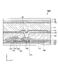
- FIG. 13 is a cross-sectional end view showing an example of the TFT 3450.
- the TFT 3450 includes, for example, a first substrate 102, an undercoat layer 1510, a gate electrode 1530, a bottom gate insulating film 1550, an oxide semiconductor layer 1570, a first connection wiring layer 1590, a top gate insulating film 1610, and a back gate electrode 1630.
- the TFT 3450 includes an overcoat layer 1730, an insulating film 1750, a first electrode 106, a first convex structure 112a, a liquid crystal layer 115, a second convex structure 112b, a second electrode 108, and a second substrate 104 in this order. Laminated.
- the undercoat layer 1510 may be composed of, for example, a silicon oxide film.
- the bottom gate insulating film 1550 may be composed of, for example, a stacked structure of SiN/SiO.
- Gate electrode 1530 may comprise, for example, molybdenum, tungsten, or alloys thereof.
- the top gate insulating film 1610 may be composed of, for example, a silicon oxide film.
- the first connection wiring layer 1590 and the second connection wiring layer 1670 may be configured with, for example, a Ti/Al/Ti laminated structure or a Mo/Al/Mo laminated structure.
- the passivation film 1650 may be composed of, for example, a silicon nitride film.
- the insulating film 1710 may be composed of, for example, a silicon oxide film or a silicon nitride film.
- the first electrode 106 may be composed of, for example, a Ti/Al/Ti laminated structure or a Mo/Al/Mo laminated structure.
- the second electrode 108 may be composed of molybdenum, tungsten, or alloys thereof, for example.
- FIG. 13 shows the TFT 3450 as a dual-gate TFT using an oxide semiconductor, amorphous silicon or low-temperature polysilicon (LTPS) may be used. Further, although an example of vertical electric field driving is shown in FIG. 13, horizontal electric field driving may be used.
- LTPS low-temperature polysilicon
- the radio wave reflector 3000 has a reflection axis 3300 parallel to the first direction and a reflection axis 3310 parallel to the second direction. Depending on the setting of the phase distribution combining the above directions, the reflection angle can be controlled in all directions forward of the radio wave reflector.
- the second electrode 108 in the phase modulation device 100 is arranged on the counter substrate 3130 .
- the second electrode 108 may be placed over the area of the counter substrate 3130 corresponding to the area where the first electrode 106 is placed.
- the radio wave reflector 3000 the plurality of first electrodes 106 are connected to the TFTs 3450 arranged in plurality.
- the radio wave reflector 3000 is configured to apply an individually independent drive voltage to the liquid crystal layer 115 from the corresponding first electrode 106 via each TFT 3450 .
- the first electrodes 106 are arranged in an array as square, circular, ring-shaped, rectangular frame-shaped, or cross-shaped patch electrodes that are symmetrical with respect to the first direction and the second direction. , By electrically connecting the first electrode 106 in the direction parallel to the reflection axis, the behavior for vertical and horizontal polarizations is adjusted to be equal, realizing high sensitivity to the target wavelength. can do. Further, by using the phase modulation device according to this embodiment as a patch electrode, a high response speed can be realized.
- phase modulation device 100 an example using the phase modulation device 100 is shown, but any of the phase modulation devices 200 to 500 described above may be used to configure the radio wave reflector.
- FIG. 14A shows a plan view of the first electrode 706.
- FIG. 14B also shows a plan view of the second electrode 708.
- FIG. 14A four first electrodes 706 may be arranged and one second electrode 708 may be arranged so as to face each other.
- FIG. 15 shows a modification of the arrangement of the first electrodes.
- the first electrodes 806x and the first electrodes 806y may be alternately arranged in a checkered pattern. Although not shown, in this case, the orientations of the second electrodes are alternately changed one by one so as to correspond to the first electrodes 806x and 806y.
- phase modulation device 102 first substrate, 104 second substrate, 106 first electrode, 108 second electrode, 112 convex structure, 112a first convex structure, 112b second convex structure, 114 liquid crystal molecules , 114 a liquid crystal molecule, 114 b liquid crystal molecule, 115 liquid crystal layer, 200 phase modulation device, 212 convex structure, 212 a first convex structure, 212 b second convex structure, 215 liquid crystal layer, 300 phase modulation device, 315 liquid crystal layer, 400 Phase modulation device 402 First substrate 404 Second substrate 406 First electrode 406S1 First slit portion 408 Second electrode 408S1 Second slit portion 408S2 Third slit portion 415 liquid crystal layer, 416 first filament portion, 416 first filament portion, 418 second filament portion, 500 phase modulation device, 502 first substrate, 504 second substrate, 506 first electrode, 506S1 first slit portion, 508 second electrode, 508S1 second slit portion, 515 liquid crystal
Landscapes
- Physics & Mathematics (AREA)
- Nonlinear Science (AREA)
- Chemical & Material Sciences (AREA)
- Crystallography & Structural Chemistry (AREA)
- General Physics & Mathematics (AREA)
- Optics & Photonics (AREA)
- Mathematical Physics (AREA)
- Geometry (AREA)
- Liquid Crystal (AREA)
Abstract
位相変調装置は、第1の電極と、第2の電極と、複数の液晶分子を含み、第1の電極と第2の電極との間に配置され液晶層と、を備え、前記第1の電極から前記第2の電極へ向かう前記液晶層の高さが30μm以上且つ50μm以下であり、第1の電極の面内方向に交差する、第1の電極、液晶層及び第2の電極を含む第1の面の平面視において、第1の電極の面内方向と平行な方向に隣接して配置され、互いに配向が異なる少なくとも2つの液晶分子を含む。
Description
本発明の一実施形態は、液晶材料が用いられた位相変調装置に関する。特に、本発明の一実施形態は、液晶材料が用いられた移相器、又はその移相器を有するフェーズドアレイアンテナ装置に関する。または、本発明の一実施形態は、液晶材料が用いられたメタマテリアル電波反射板に関する。
フェーズドアレイアンテナ(Phased Array Antenna)装置は、複数のアンテナ素子の一部又は全部にそれぞれ高周波信号を印加するときに、それぞれの高周波信号の振幅と位相を制御することで、アンテナの向きを一方向に固定したままで、アンテナの放射指向性を制御できるという特性を有する。フェーズドアレイアンテナ装置は、アンテナ素子に印加する高周波信号の位相を制御するために移相器が用いられている。
移相器の方式としては、伝送線路の長さを物理的に変化させて高周波信号の位相を変化させる方式、伝送線路の途中でインピーダンスを変化させ反射により高周波の位相をさせる方式、位相が異なる2つの信号を増幅する増幅器の利得を制御して合成することで所望の位相を有する信号を生成する方式など様々な方式が採用されている。また、これら以外にも、特許文献1には、移相器の一例として、印加する電圧によって誘電率が変化するという液晶材料特有の性質を利用する方式が開示されている。
一方、液晶の誘電率異方性を利用し、パッチ電極に入射した電波の反射波に位相変化を与えるメタマテリアル反射板が知られている。メタマテリアル反射板は、隣り合うパッチ電極にそれぞれ異なる電圧を印加することにより、各々での位相変化量を異ならせ、見かけ上、電波の反射方向が変わったように振る舞わせることが可能である。例えば、特許文献2には、反射位相が電子的に再構成され、電子的に調整可能なメタサーフェスが開示されている。
Y. Iimura, S. Kobayashi, T. Sugiyama, Y. Toko, T. Hashimoto, K. Kato," EO Characteristics of Amorphous and Super-Multidomain TN-LCDs Prepared by a Non-Rubbing Method" The institute of Image Information and Television Engineers Technical Report, Volume 18 (Issue 43), pp.31-36, 1994.
液晶を用いた移相器やメタマテリアル反射板等の位相変調装置において、十分な位相変化量を得るためには、液晶ディスプレイと比較すると、液晶層の厚み(セルギャップ)が10倍以上も必要となるため、応答速度が数秒程度まで遅くなるという課題があった。より高速な応答速度を実現し得る位相変調装置が求められている。
本発明の一実施形態に係る位相変調装置は、第1の電極と、第2の電極と、複数の液晶分子を含み、第1の電極と第2の電極との間に配置され液晶層と、を備え、第1の電極と第2の電極との間の距離が30μm以上且つ50μm以下であり、第1の電極の面内方向に交差する、第1の電極、液晶層及び第2の電極を含む第1の面の平面視において、第1の電極の面内方向と平行な方向に隣接して配置され、互いに配向が異なる少なくとも2つの液晶分子を含む。
以下、本発明の実施の形態を、図面等を参照しながら説明する。但し、本発明は多くの異なる態様で実施することが可能であり、以下に例示する実施の形態の記載内容に限定して解釈されるものではない。図面は説明をより明確にするため、実際の態様に比べ、各部の幅、厚さ、形状等について模式的に表される場合があるが、あくまで一例であって、本発明の解釈を限定するものではない。また、本明細書と各図において、既出の図に関して前述したものと同様の要素には、同一の符号(又は数字の後にa、bなどを付した符号)を付して、詳細な説明を適宜省略することがある。さらに各要素に対する「第1」、「第2」と付記された文字は、各要素を区別するために用いられる便宜的な標識であり、特段
の説明がない限りそれ以上の意味を有しない。
の説明がない限りそれ以上の意味を有しない。
本明細書において、ある部材又は領域が他の部材又は領域の「上に(又は下に)」あるとする場合、特段の限定がない限りこれは他の部材又は領域の直上(又は直下)にある場合のみでなく他の部材又は領域の上方(又は下方)にある場合を含み、すなわち、他の部材又は領域の上方(又は下方)において間に別の構成要素が含まれている場合も含む。なお、以下の説明では、特に断りのない限り、断面視において、図の正位置に対して上方を「上」又は「上方」といい、「上」又は「上方」から見た面を「上面」又は「上面側」というものとし、その逆を「下」、「下方」、「下面」又は「下面側」というものとする。
図1Aに、本発明の一実施形態に係る位相変調装置100の平面図を示す。位相変調装置100は、第1の電極106と、第2の電極108とが、対向するように配置された構造を有する。は、第1の電極106から第2の電極108を見た平面視、又は第2の電極108から第1の電極106を見た平面視において、略同一の平板形状を有するが、第1の電極106と第2の電極108とは、これに限定されない。例えば、第2の電極108がグランド電極である場合には、第2の電極108よりも、第1の電極106のY軸方向(後述する第2の方向)の幅が短くてもよい。
図1Bに、第1の基板102の平面図を示す。第1の基板102は平板状の基体であり、絶縁表面を有している。第1の電極106は、この絶縁表面上に設けられている。図1Bにおいては、一例として、第1の基板102と略同一の第1の電極106が配置された構造を示したが、第1の基板102に対して、第1の電極106のY軸方向の幅が短くてもよい。
第1の電極106は、第1の基板102の表面に少なくとも1層の導電膜を形成することにより、作製することができる。または、形成した導電膜をエッチングによりパターニングすることにより、第1の基板102又は第2の電極108に対して、Y軸方向の幅が短くなるように、第1の電極106を作製してもよい。第1の基板102は、ガラス、セラミック等の絶縁材料で形成され、それ自体の物性により絶縁表面が形成されていてもよいし、表面に絶縁膜が形成されることによって絶縁表面が形成されていてもよい。導電膜は、アルミニウム、銅等の金属膜であり、真空蒸着、スパッタリングによって作製することができる。また、導電膜に代えて金属箔が第1の電極106として用いられてもよい。
図1Cに、第2の基板104の平面図を示す。第2の基板104は平板状の基体であり、絶縁表面を有している。第2の基板104の一主面には、略全面に第2の電極108が設けられている。第2の電極108もまた、導電膜によって形成されている。
図2Aは、図1Aに示すA1-A2線に沿った断面構造について、破線で囲んだ部分Aの断面構造を示す。第1の電極106と第2の電極108との間には、液晶層115が配置される。液晶層115には、液晶が充填されており、換言すれば、液晶層115は、複数の液晶分子114を含む。第1の電極106から第2の電極108へ向かうZ軸方向の液晶層115の高さdは、30μm以上50μm以下である。図2Aに示したように、第1の電極106の面内方向に交差する、第1の電極106、液晶層115及び第2の電極108を含む断面(以下、第1の面とも称する)の平面視において、第1の電極106の面内方向と平行な方向に隣接して配置された2つの液晶分子114は、互いに配向が異なる。位相変調装置100は、このような隣接する少なくとも2つの液晶分子114の配向が異なるように液晶分子114の配向を制御することを特徴とする。
一実施形態において、液晶分子114aは、第1の電極106に対して傾斜しており(第1の傾斜角)、第1の電極106の面内方向と平行な方向に隣接して配置された液晶分子114bは、第1の傾斜角とは異なる第2の傾斜角で、第1の電極106に対して傾斜している。
このような液晶分子114の配向制御は、一実施形態において、位相変調装置100に凸構造112を配置することにより、実現することができる。第1の電極106には、第2の電極108に向かって突出した複数の第1の凸構造112aが配置される。また、第2の電極108には、第1の電極106に向かって突出した複数の第2の凸構造112bが配置される。なお、第1の電極106に複数の第1の凸構造112aが配置されることにより、液晶分子114の配向を制御することは可能である。したがって、第2の凸構造112bを配置しない構成であっても、液晶分子114の配向制御が可能である。
図2Bは、図2Aに示した破線部Bで囲まれた凸構造112を示す拡大図である。なお、図2Bに示した凸構造112は、第1の凸構造112aと第2の凸構造112bに適用される。凸構造112は、第1の面での断面視において三角形状の断面を有する。凸構造112は、第1の電極106の面内方向と平行な第1の方向(X軸方向)に延伸し、且つ第1の方向に直交する第2の方向(Y軸方向)に配置された複数の三角柱状の構造を有する。一実施形態において、三角形状の断面は、三角形状の底面に対して、3°~5°の傾斜角θを有する二等辺三角形である。三角形状の断面は、液晶層115の高さdに対して、1/20~1/10の高さhを有する(h=d/20~d/10)。
また、図2Aに示したように、第1の凸構造112aと第2の凸構造112bとは対向するように配置される。しかし、第2の電極108に向かって突出した第1の凸構造112aの角部(第1の角部)は、第1の電極106に向かって突出した第2の凸構造112bの角部(第2の角部)とは、第2の方向(Y軸方向)に対して所定の距離lだけ離隔して配置される。換言すると、第1の角部から第2の電極108に向う垂線は、第2の角部から第1の電極106に向う垂線とは、平行な位置関係となり、一致しない。このような第1の凸構造112aと第2の凸構造112bとの配置により、第1の電極106から第2の電極108に向う複数の液晶分子114が配置される区画が、幅lにより規定される。本実施形態おいて、区画の幅lは、液晶層115の高さdよりも小さい(l<d)。
一例として、液晶層115の高さdを30μm~50μmとしたときに、凸構造112は、底辺が34~57μm、傾斜角が3~5°、高さが3μmとなる三角形状の断面を有する構造であってもよい。または、凸構造112は、底辺が5.7μm、傾斜角が3~5°、高さが0.3μm~0.5μmとなる三角形状の断面を有する構造であってもよい。
液晶分子114の配向制御は、例えば、液晶表示装置においては公知の技術ではあるが、液晶表示装置は、位相変調装置100のような30μm~50μmの液晶層115の高さには設計されない。このような液晶層115の厚みは、位相変調装置100に特有の構造である。また、視認性を要求される液晶表示装置においては、液晶分子114は、液晶層115の高さdよりも小さい幅lの区画には配置されない。このような、小さな区画を用いた液晶分子114の配向制御は、従来用いられていない技術である。位相変調装置100においては、このような、小さな区画により液晶分子114を配向制御するため、従来にない高速な位相変調制御を実現することができる。本実施形態においては、誘電率の変化量を最大化することができる。
このような凸構造112は、感光性有機膜と配向膜とを積層して実現することができる。感光性有機膜の材料としては、液晶表示装置のアレイ基板に含まれる有機平坦化膜に用いる感光性有機膜としての公知の樹脂、例えば、アクリル系樹脂やポリイミド樹脂等を用いることができる。第1の電極106及び第2の電極108の表面にポリイミド等の樹脂を塗布し、感光、現像を経て凸構造を形成した上で、ラビング法を用いて、液晶が配向する凸構造112を形成することができる。
図3Aに、凸構造112の変形例である凸構造212を配置した位相変調装置200の第1の面における断面端図を示す。図3Bは、図3Aに示した破線部Bで囲まれた凸構造212を示す拡大図である。なお、図3Bに示した凸構造212は、第1の凸構造212aと第2の凸構造212bに適用される。凸構造212は、第1の面での断面視において三角形状の断面を有するが、凸構造112と比較すると、その底辺は小さく、第1の電極106に配置した突起である。
凸構造212は、第1の電極106の面内方向と平行な第1の方向(X軸方向)に延伸し、且つ第1の方向に直交する第2の方向(Y軸方向)に配置された複数の三角柱状の構造を有する。一実施形態において、三角形状の断面は、液晶層215の高さdに対して、1/20~1/10の高さh(h=d/20~d/10)を備えていればよく、底辺の長さや傾斜角は特には限定されない。
また、図3Aに示したように、第1の凸構造212aと第2の凸構造212bとは対向するように配置される。しかし、第2の電極108に向かって突出した第1の凸構造212aの角部(第1の角部)は、第1の電極106に向かって突出した第2の凸構造212bの角部(第2の角部)とは、第2の方向(Y軸方向)に対して所定の距離lだけ離隔して配置される。換言すると、第1の角部から第2の電極108に向う垂線は、第2の角部から第1の電極106に向う垂線とは、平行な位置関係となり、一致しない。このような第1の凸構造212aと第2の凸構造212bとの配置により、第1の電極106から第2の電極108に向う複数の液晶分子114が配置される区画が、幅lにより規定される。本実施形態おいて、区画の幅lは、液晶層215の高さdよりも小さい(l<d)。
このような凸構造212は、凸構造112と同様の材料及び製造方法により作成することができため、詳細な説明は省略する。
上述した液晶分子114の配向制御は、一実施形態において、液晶層をアモルファス化することにより、実現することもできる。図4Aは、液晶層315をアモルファス化した位相変調装置300の第1の面における断面端図を示す。図4Bは、アモルファス化した液晶層315を第1の電極106から観察した図である(非特許文献1より引用)。図4Bにおいて観察される干渉縞は、配向が異なる液晶分子114が隣接した境界、即ち区画を示す。液晶層315は、液晶分子114がランダムに配向した構造を備えている。また、区画の幅l1と、隣接する区画の幅l2とは異なることも液晶層315の特徴であり、液晶層315全体として規則性は示さない。また、液晶層315の高さdを30μm~50μmであり、本実施形態おいても、区画の幅l1や幅l2は、液晶層315の高さdよりも小さい(l<d)。
本明細書において、「ランダムに配向した構造」とは、液晶層315に含まれる液晶分子114の配向が、全体として規則性を示さないことを意味し、微視的な観察において同じ配向を有する液晶分子が隣接して配置されることを排除するものではない。
このような液晶層315は、第1の電極106と第2の電極108とのいずれか一方、あるいは双方の表面を覆うように配向膜を塗布した後、ラビング等の配向処理を行わず、第1の電極106と第2の電極108との間の空間に液晶分子114を封入し、等方相まで加熱した後に急冷してカイラルネマティック層を形成することにより実現することができる。なお、少なくとも第1の電極106上には、配向膜を配置する。
本実施形態においては、液晶層315をアモルファス化することにより、区画の幅lを液晶層315の高さdよりも小さくすることにより、液晶分子114の高速な配向制御を実現することができる。
液晶層における区画を形成する方法として、第1の電極406と第2の電極408の配置を用いる実施形態について説明する。図5Aに、本発明の一実施形態に係る位相変調装置400の平面図を示す。本実施形態においては、第1の電極406及び第2の電極408はストリップ状の構造である。また、第1の電極406から第2の電極408に向かった方向での平面視において、第1の電極406と第2の電極408の配置をずらすことにより、第1の電極406に対して、電界を斜めに生じさせることにより液晶分子114の配向を制御する。
図5B及び図5Cを参照して、より詳細に説明する。図5Bに、第1の基板402の平面図を示す。第1の基板402の構成は、第1の基板102の構成と同様の構成であってもよく、詳細な説明は省略する。第1の電極406は、第1の電極406の面内方向と平行な第1の方向(X軸方向)に延伸し、且つ第1の方向に直交する第2の方向(Y軸方向)に配置された複数の線条部(第1の線条部)416を備える。また、第1の電極406は、複数の第1の線条部416の間にそれぞれ配置されたスリット部(第1のスリット部)406S1を備える。第1の電極406は、上述した第1の電極106に対して形状が異なるが、その材料や製造方法については、第1の電極106と同様の構成であってもよく、詳細な説明は省略する。
図5Cに、第2の基板404の平面図を示す。第2の基板404の構成は、第2の基板104の構成と同様の構成であってもよく、詳細な説明は省略する。第2の電極408は、第1の方向(X軸方向)に延伸し、且つ第2の方向(Y軸方向)に配置された複数の第2の線条部418を備える。また、第2の電極408は、複数の第2の線条部418の間にそれぞれ配置された第2のスリット部(408S1及び408S2)を備える。第2の電極408は、上述した第2の電極108に対して形状が異なるが、その材料や製造方法については、第2の電極108と同様の構成であってもよく、詳細な説明は省略する。
図6を参照する。図6は、図5Aに示すA1-A2線に沿った断面構造について、破線で囲んだ部分Aの断面構造を示す。第1の電極406と第2の電極408との間には、液晶層415が配置される。液晶層415には、液晶が充填されており、換言すれば、液晶層415は、複数の液晶分子114を含む。第1の電極406から第2の電極408へ向かうZ軸方向の液晶層415の高さdは、30μm以上50μm以下である。
位相変調装置400において、第1の線条部416の第2の方向(Y軸方向)の幅と、第2の線条部418の第2の方向の幅は同じである。第1の電極406において、第1の線条部416の間に配置された第1のスリット部406S1の第2の方向の幅W1はそれぞれ同じである。したがって、第1の線条部416が第2の方向に等間隔に配置されることにより、第1の電極406が構成される。一方、第2の電極408において、第2の線条部418の間に配置された第2のスリット部408S1の第2の方向の幅W2と、第3のスリット部408S2の第2の方向の幅W3とは互いに異なる。第2の電極408においては、w2>w3の関係にある。また、第2のスリット部408S1と、前記第3のスリット部408S2とは、第2の方向に交互に配置される。
さらに、位相変調装置400においては、w2>w1>w3の関係にある。このため、図5Aにも示したように、位相変調装置400においては、第1の電極406から第2の電極408に向かった方向での平面視において、複数の第1の線条部416は、第2の方向(Y軸方向)において、複数の第2の線条部418の一部分のみとそれぞれ重畳するように配置される。なお、第1の電極406の構成と第2の電極408の構成を逆にしてもよい。
位相変調装置400においては、このような第1の電極406と第2の電極408との配置により第1の電極406から第2の電極408に向う複数の液晶分子114が配置される区画が、幅lにより規定される。本実施形態おいて、区画の幅lは、液晶層415の高さdよりも小さい(l<d)。なお、第1の電極から第2の電極に向かった方向での平面視において、第1のスリット部406S1と第2のスリット部408S1とが重畳する位置、及び第1のスリット部406S1と第3のスリット部408S2とが重畳する位置においては、液晶分子114の位相変化が生じないため、液晶層415における区画を形成可能な範囲で、w1、w2及びw3を小さくすることが好ましい。
位相変調装置400において説明した第1の電極406と第2の電極408との配置は、視認性を要求される液晶表示装置においては選択されることのない配置であり、30μm~50μmの液晶層415の高さには設計される位相変調装置400に特有の構造である。位相変調装置400においては、このような、小さな区画により液晶分子114を配向制御するため、従来にない高速な位相変調制御を実現することができる。
位相変調装置400においては、第1のスリット部406S1の幅が一定である場合に、第2のスリット部408S1と第3のスリット部408S2との幅を調整することにより、液晶分子114を配向制御する方法を説明した。位相変調装置500においては、第1のスリット部506S1と第2のスリット部508S1の幅が同じ場合に、第1の電極506と第2の電極508とが平面視で重畳する位置を調整することにより、液晶分子114を配向制御する方法を説明する。
図7Aに、本発明の一実施形態に係る位相変調装置500の平面図を示す。本実施形態においては、第1の電極506及び第2の電極508はストリップ状の構造である。また、第1の電極506から前記第2の電極508に向かった方向での平面視において、第1の電極506と第2の電極508の配置をずらすことにより、第1の電極506に対して、電界を斜めに生じさせることにより液晶分子114の配向を制御する。
図7B及び図7Cを参照して、より詳細に説明する。図7Bに、第1の基板502の平面図を示す。第1の基板502の構成は、第1の基板102の構成と同様の構成であってもよく、詳細な説明は省略する。第1の電極506は、第1の電極506の面内方向と平行な第1の方向(X軸方向)に延伸し、且つ第1の方向に直交する第2の方向(Y軸方向)に配置された複数の線条部(第1の線条部516)を備える。また、第1の電極506は、複数の第1の線条部516の間にそれぞれ配置されたスリット部(第1のスリット部)506S1を備える。第1の電極506は、上述した第1の電極106に対して形状が異なるが、その材料や製造方法については、第1の電極106と同様の構成であってもよく、詳細な説明は省略する。
図7Cに、第2の基板504の平面図を示す。第2の基板504の構成は、第2の基板104の構成と同様の構成であってもよく、詳細な説明は省略する。第2の電極508は、第1の方向(X軸方向)に延伸し、且つ第2の方向(Y軸方向)に配置された複数の第2の線条部518を備える。また、第2の電極508は、複数の第2の線条部518の間にそれぞれ配置された第2のスリット部508S1を備える。第2の電極508は、上述した第2の電極108に対して形状が異なるが、その材料や製造方法については、第2の電極108と同様の構成であってもよく、詳細な説明は省略する。
図8を参照する。図8は、図7Aに示すA1-A2線に沿った断面構造について、破線で囲んだ部分Aの断面構造を示す。第1の電極506と第2の電極508との間には、液晶層515が配置される。液晶層515には、液晶が充填されており、換言すれば、液晶層515は、複数の液晶分子114を含む。第1の電極506から第2の電極508へ向かうZ軸方向の液晶層515の高さdは、30μm以上50μm以下である。
第1の電極506において、第1の線条部516の間に配置された第1のスリット部506S1の第2の方向の幅ws1はそれぞれ同じである。また、第2の電極508において、第2の線条部518の間に配置された第2のスリット部508S1の第2の方向の幅ws2もそれぞれ同じである。さらに、ws1=ws2の関係にある。一方、位相変調装置500において、第1の電極506を構成する第1の線条部516の第2の方向(Y軸方向)の幅we1と、第2の電極508を構成する第2の線条部518の第2の方向(Y方向)の幅we2もそれぞれ同じであり、we1=we2の関係にある。
図7Aにも示したように、位相変調装置500においては、第1の電極506から第2の電極508に向かった方向での平面視において、第1の線条部516は、2つの第2の線条部518と、一部分が重畳する。さらに、第2の線条部518は、2つの第1の線条部516と、一部分が重畳するように配置される。なお、第1の電極506の構成と第2の電極508の構成を逆にしてもよい。また、面内の応答速度を均等化させるために、それぞれの重畳幅が一定となるように配置することが好ましい。
位相変調装置500においては、このような第1の電極506と第2の電極508との配置により第1の電極506から第2の電極508に向う複数の液晶分子114が配置される区画が、幅lにより規定される。本実施形態おいて、区画の幅lは、液晶層515の高さdよりも小さい(l<d)。なお、第1の電極506から第2の電極508に向かった方向での平面視において、第1のスリット部506S1と第2の線条部518が重畳する位置、及び第2のスリット部508S1と第1の線条部516が重畳する位置においては、液晶分子114の位相変化が生じないため、液晶層515における区画を形成可能な範囲で、ws1及びws2を小さくすることが好ましい。
位相変調装置500において説明した第1の電極506と第2の電極508との配置は、視認性を要求される液晶表示装置においては選択されることのない配置であり、30μm~50μmの液晶層515の高さには設計される位相変調装置500に特有の構造である。位相変調装置500においては、このような、小さな区画により液晶分子114を配向制御するため、従来にない高速な位相変調制御を実現することができる。
[フェーズドアレイアンテナ装置]
上述した各実施形態より説明した位相変調装置を、移相器として用いることができる。位相変調装置を移相器として用いることにより、高速な応答速度を実現するフェーズドアレイアンテナ装置を構成することができる。図9は、移相器として位相変調装置100が用いられたフェーズドアレイアンテナ装置1000の一構成例を示す。図9は、フェーズドアレイアンテナ装置1000の平面図を示す。また、図10は、図9においてB1-B2線に対応する断面構造を示す。以下においては、図9及び図10を参照して説明する。
上述した各実施形態より説明した位相変調装置を、移相器として用いることができる。位相変調装置を移相器として用いることにより、高速な応答速度を実現するフェーズドアレイアンテナ装置を構成することができる。図9は、移相器として位相変調装置100が用いられたフェーズドアレイアンテナ装置1000の一構成例を示す。図9は、フェーズドアレイアンテナ装置1000の平面図を示す。また、図10は、図9においてB1-B2線に対応する断面構造を示す。以下においては、図9及び図10を参照して説明する。
フェーズドアレイアンテナ装置1000は、位相変調装置100とアンテナ素子1130を含む。アンテナ素子1130は、直線状、円弧状、面状に複数個が配列されてアンテナ素子アレイを形成する。位相変調装置100は複数のアンテナ素子1130のそれぞれに対応して設けられる。また、フェーズドアレイアンテナ装置1000は、図示されない位相制御回路を有している。位相制御回路は位相変調装置100の位相を制御する信号を出力する機能を有している。
なお、図9及び図10は、フェーズドアレイアンテナ装置1000が送信用である場合を示す。フェーズドアレイアンテナ装置1000は、マイクロストリップ線路である第1の電極106のそれぞれと接続される端子部1160を有している。各端子部1160は、分配器1180と接続されている。分配器1180は発振器1200と接続されている。発振器1200から出力された高周波信号は、分配器1180によってそれぞれの位相変調装置100に分配される。
複数のアンテナ素子1130のそれぞれから放射される電磁波はコヒーレント性を有している。そのため、複数のアンテナ素子1130のそれぞれから放射される電磁波によって、位相が揃った波面が形成される。アンテナ素子1130から放射される電磁波の位相は位相変調装置100によって調整される。位相変調装置100は、図示されない位相制御回路によって、電磁波として放射される高周波信号の位相が制御される。位相変調装置100はマイクロストリップ線路である第1の電極106での損失を低減するため線幅が広げられているものの、接地導体層である第2の電極108との間に凸構造112を配置することにより、液晶の応答速度の高速化を実現している。なお、フェーズドアレイアンテナ装置1000を受信用に使用する場合も同様の効果を得ることができる。
上述したフェーズドアレイアンテナ装置においては、位相変調装置100を用いた例を示したが、上述した位相変調装置200~500の何れの位相変調装置を用いてフェーズドアレイアンテナ装置を構成してもよい。
[電波反射板]
上述した各実施形態より説明した位相変調装置を、パッチ電極として用いることにより、高速な応答速度を実現するメタマテリアル反射板を構成することができる。図11は、パッチ電極に対応させて位相変調装置100を用いた電波反射板2000の一構成例を示す。図11は、一軸反射制御の電波反射板2000の平面図を示す。電波反射板2000は、アレイ基板2100と対向基板2130が対向するように配置され、アレイ基板2100と対向基板2130との間には液晶層115が配置されている。液晶層115は、シール2150により封止されている。アレイ基板2100には、複数の第1の電極106が第1の方向(X軸方向)に配置され、且つ複数の第1の電極106が第1の方向に直交する第2の方向(Y軸方向)にも配置されている。第1の方向に配置された複数の第1の電極106は、細線パターン2410により電気的に接続される。駆動回路2170と、細線パターン2410とは、配線2195により電気的に接続される。また、電波反射板2000は、第1の方向に平行な反射軸2300を有する。
上述した各実施形態より説明した位相変調装置を、パッチ電極として用いることにより、高速な応答速度を実現するメタマテリアル反射板を構成することができる。図11は、パッチ電極に対応させて位相変調装置100を用いた電波反射板2000の一構成例を示す。図11は、一軸反射制御の電波反射板2000の平面図を示す。電波反射板2000は、アレイ基板2100と対向基板2130が対向するように配置され、アレイ基板2100と対向基板2130との間には液晶層115が配置されている。液晶層115は、シール2150により封止されている。アレイ基板2100には、複数の第1の電極106が第1の方向(X軸方向)に配置され、且つ複数の第1の電極106が第1の方向に直交する第2の方向(Y軸方向)にも配置されている。第1の方向に配置された複数の第1の電極106は、細線パターン2410により電気的に接続される。駆動回路2170と、細線パターン2410とは、配線2195により電気的に接続される。また、電波反射板2000は、第1の方向に平行な反射軸2300を有する。
位相変調装置100における第2の電極108は、対向基板2130に配置される。一実施形態において、第1の電極106が配置された領域に対応する対向基板2130の領域全体に第2の電極108が配置されてもよい。
電波反射板2000においては、細線パターン2410により電気的に接続された第1の電極106の方向(第1の方向)の一列に同一信号を入力するため、図11において破線で囲んだ、反射軸2300に平行な一列方向のパッチ電極は全て互いに電気的に接続される。
本実施形態においては、第1の電極106を第1の方向及び第2の方向に対して対称となる正方形、円形、円環形、矩形枠形(中空とした矩形)、又は十字形のパッチ電極としてアレイ状に配置し、反射軸に平行な方向に第1の電極106を電気的に接続することにより、垂直偏波と水平偏波とに対する振る舞いが等しくなるように調整し、目的の波長に対して高い感度を実現することができる。また、本実施形態に係る位相変調装置を、パッチ電極として用いることにより、高速な応答速度を実現することができる。
上述した電波反射板2000は、反射軸2300が1つのみであったため、反射軸2300を回転軸とした方向のみ、反射角を制御することができる。二軸反射制御の電波反射板3000について、以下に説明する。図12Aは、パッチ電極に対応させて位相変調装置100を用いた電波反射板3000の一構成例を示す。図12Aは、二軸反射制御の電波反射板3000の平面図を示す。電波反射板3000は、アレイ基板3100と対向基板3130が対向するように配置され、アレイ基板3100と対向基板3130との間には液晶層115が配置されている。液晶層115は、シール3150により封止されている。アレイ基板3100には、複数の第1の電極106が第1の方向(X軸方向)に配置され、且つ複数の第1の電極106が第1の方向に直交する第2の方向(Y軸方向)にも配置されている。第1の方向に配置された複数の第1の電極106は、細線パターン3410により電気的に接続される。信号線駆動回路3170と、細線パターン3410とは、配線3195により電気的に接続される。また、電波反射板3000は、第1の方向に平行な反射軸3300を有する。
また、第2の方向に配置された複数の第1の電極106は、細線パターン3430により電気的に接続される。細線パターン3430は、走査線駆動回路3190に電気的に接続される。また、電波反射板3000は、第2の方向に平行な反射軸3310を有する。
図12Bは、図12Aの破線部Eを拡大した平面である。細線パターン3410と細線パターン3430は、薄膜トランジスタ(TFT)3450に接続する。図13は、TFT3450の一例を示す断面端図である。TFT3450は、例えば、第1の基板102、アンダーコート層1510、ゲート電極1530、ボトムゲート絶縁膜1550、酸化物半導体層1570、第1の接続配線層1590、トップゲート絶縁膜1610、バックゲート電極1630、パッシベーション膜1650、第2の接続配線層1670、信号線1690、絶縁膜1710が順次積層した構造を有する。TFT3450には、オーバーコート層1730、絶縁膜1750、第1の電極106、第1の凸構造112a、液晶層115、第2の凸構造112b、第2の電極108、第2の基板104が順次積層される。
アンダーコート層1510は、例えば、シリコン酸化膜で構成されてもよい。ボトムゲート絶縁膜1550は、例えば、SiN/SiOの積層構造で構成されてもよい。ゲート電極1530は、例えば、モリブデン、タングステン又はこれらの合金で構成されてもよい。トップゲート絶縁膜1610は、例えば、シリコン酸化膜で構成されてもよい。また、第1の接続配線層1590及び第2の接続配線層1670は、例えば、Ti/Al/Tiの積層構造、又はMo/Al/Moの積層構造で構成されてもよい。パッシベーション膜1650は、例えば、窒化シリコン膜で構成されてもよい。絶縁膜1710は、例えば、シリコン酸化膜又は窒化シリコン膜で構成されてもよい。第1の電極106は、例えば、Ti/Al/Tiの積層構造、又はMo/Al/Moの積層構造で構成されてもよい。第2の電極108は、例えば、モリブデン、タングステン又はこれらの合金で構成されてもよい。
なお、図13においては、TFT3450を、酸化物半導体を用いたデュアルゲート型TFTとして示しているが、アモルファスシリコンを用いてもよく、低温ポリシリコン(LTPS)を用いてもよい。また、図13においては、縦電界駆動の例を示したが、横電界駆動を用いてもよい。
電波反射板3000は、第1の方向に平行な反射軸3300と、第2の方向に平行な反射軸3310を有するため、反射軸3300を回転軸とした方向、及び反射軸3310を回転軸とした方向を組み合わせた位相分布の設定次第で、当該電波反射板の前方全方位に対して、反射角を制御することができる。
位相変調装置100における第2の電極108は、対向基板3130に配置される。一実施形態において、第1の電極106が配置された領域に対応する対向基板3130の領域全体に第2の電極108が配置されてもよい。
電波反射板3000においては、複数の第1の電極106は、複数配置されたTFT3450にそれぞれ接続される。これにより、電波反射板3000は、各TFT3450を介して対応する第1の電極106から個々に独立した駆動電圧を液晶層115に印加するように構成される。
本実施形態においては、第1の電極106を第1の方向及び第2の方向に対して対称となる正方形、円形、円環形、矩形枠形、又は十字形のパッチ電極としてアレイ状に配置し、反射軸に平行な方向に第1の電極106を電気的に接続することにより、垂直偏波と水平偏波とに対する振る舞いが等しくなるように調整し、目的の波長に対して高い感度を実現することができる。また、本実施形態に係る位相変調装置を、パッチ電極として用いることにより、高速な応答速度を実現することができる。
上述した電波反射板においては、位相変調装置100を用いた例を示したが、上述した位相変調装置200~500の何れの位相変調装置を用いて電波反射板を構成してもよい。
上述した位相変調装置400を電波反射板2000又は電波反射板3000に適用する例について説明する。図14Aは、第1の電極706の平面図を示す。また、図14Bは、第2の電極708の平面図を示す。また、図14Aにおいて、4つの第1の電極706を配置し、1つの第2の電極708を対向するように配置する構成としてもよい。
図15に、第1の電極の配置の変形例を示す。第1の電極806xと第1の電極806yを交互に、市松模様のように配置してもよい。図示しないが、この場合には、第1の電極806xと第1の電極806yに対応するように、第2の電極も1つ1つ交互に向きを変えた配置である。
100 位相変調装置、102 第1の基板、104 第2の基板、106 第1の電極、108 第2の電極、112 凸構造、112a 第1の凸構造、112b 第2の凸構造、114 液晶分子、114a 液晶分子、114b 液晶分子、115 液晶層、200 位相変調装置、212 凸構造、212a 第1の凸構造、212b 第2の凸構造、215 液晶層、300 位相変調装置、315 液晶層、400 位相変調装置、402 第1の基板、404 第2の基板、406 第1の電極、406S1 第1のスリット部、408 第2の電極、408S1 第2のスリット部、408S2 第3のスリット部、415 液晶層、416 第1の線条部、416 第1の線条部、418 第2の線条部、500 位相変調装置、502 第1の基板、504 第2の基板、506 第1の電極、506S1 第1のスリット部、508 第2の電極、508S1 第2のスリット部、515 液晶層、516 第1の線条部、517 第3の線条部、518 第2の線条部、706 第1の電極、708 第2の電極、806x 第1の電極、806y 第1の電極、1000 フェーズドアレイアンテナ装置、1130 アンテナ素子、1160 端子部、1180 分配器、1200 発振器、1510 アンダーコート層、1530 ゲート電極、1550 ボトムゲート絶縁膜、1570 酸化物半導体層、1590 第1の接続配線層、1610 トップゲート絶縁膜、1630 バックゲート電極、1650 パッシベーション膜、1670 第2の接続配線層、1690 信号線、1710 絶縁膜、1730 オーバーコート層、1750 絶縁膜、2000 電波反射板、2019 特表、2100 アレイ基板、2130 対向基板、2150 シール、2170 駆動回路、2195 配線、2300 反射軸、2410 細線パターン、3000 電波反射板、3100 アレイ基板、3130 対向基板、3150 シール、3170 信号線駆動回路、3190 走査線駆動回路、3195 配線、3300 反射軸、3310 反射軸、3410 細線パターン、3430 細線パターン
Claims (14)
- 第1の電極と、第2の電極と、複数の液晶分子を含み、前記第1の電極と前記第2の電極との間に配置され液晶層と、を備え、
前記第1の電極から前記第2の電極へ向かう前記液晶層の高さが30μm以上且つ50μm以下であり、
前記第1の電極の面内方向に交差する、前記第1の電極、前記液晶層及び前記第2の電極を含む第1の面の平面視において、前記第1の電極の面内方向と平行な方向に隣接して配置され、互いに配向が異なる少なくとも2つの液晶分子を含む、位相変調装置。 - 前記第1の面において、前記第1の電極に対して、第1の傾斜角を有する液晶分子と、前記第1の電極の面内方向と平行な方向に隣接して配置され、前記第1の傾斜角とは異なる第2の傾斜角を有する液晶分子と、を含む請求項1に記載の位相変調装置。
- 前記第1の電極に配置され、前記第2の電極に向かって突出した複数の第1の凸構造をさらに備え、
前記複数の第1の凸構造は、前記第1の面での断面視において三角形状の断面を有し、前記第1の電極の面内方向と平行な第1の方向に延伸し、且つ前記第1の方向に直交する第2の方向に配置された複数の三角柱状の構造を有する、請求項1に記載の位相変調装置。 - 前記第2の電極に配置され、前記第1の電極に向かって突出した複数の第2の凸構造をさらに備え、
前記複数の第2の凸構造は、前記第1の面での断面視において三角形状の断面を有し、前記第1の電極の面内方向と平行な第1の方向に延伸し、且つ前記第1の方向に直交する第2の方向に配置された複数の三角柱状の構造を有し、
前記複数の第1の凸構造の前記第2の電極に向かって突出した第1の角部と、前記複数の第2の凸構造の前記第1の電極に向かって突出した第2の角部とは、前記第2の方向に対して所定の距離だけ離隔する、請求項3に記載の位相変調装置。 - 前記第1の面の平面視において、前記三角形状の断面は、前記液晶層の高さに対して、1/20~1/10の高さを有する、請求項3に記載の位相変調装置。
- 前記第1の面の平面視において、前記三角形状の断面は、前記三角形状の底面に対して、3°~5°の傾斜角を有する、請求項5に記載の位相変調装置。
- 前記第1の電極は、前記第1の電極の面内方向と平行な第1の方向に延伸し、且つ前記第1の方向に直交する第2の方向に配置された複数の第1の線条部と、前記複数の第1の線条部の間にそれぞれ配置された第1のスリット部と、を備え、
前記第2の電極は、前記第1の方向に延伸し、且つ前記第2の方向に配置された複数の第2の線条部と、前記複数の第2の線条部の間にそれぞれ配置された第2のスリット部と、を備え、
前記第1の電極から前記第2の電極に向かった方向での平面視において、前記複数の第1の線条部は、前記第2の方向において、前記複数の第2の線条部の一部分のみとそれぞれ重畳する、請求項1に記載の位相変調装置。 - 前記第2の電極は、第2のスリット部とは前記第2の方向に対する幅が異なる第3のスリット部を有し、
前記第2の電極において、前記第2のスリット部と、前記第3のスリット部とは、前記第2の方向に交互に配置される、請求項7に記載の位相変調装置。 - 前記第1の電極から前記第2の電極に向かった方向での平面視において、前記複数の第1の線条部の中の1つの第1の線条部は、前記複数の第2の線条部の中の2つの第2の線条部と、一部分が重畳する、請求項7に記載の位相変調装置。
- 請求項1乃至9のいずれか一項に記載の位相変調装置を含み、
前記第1の電極がマイクロストリップ線路であり、前記第2の電極が接地導体層である、移相器。 - 請求項10に記載の移相器を有するフェーズドアレイアンテナ装置。
- 請求項1乃至9のいずれか一項に記載の位相変調装置を含む電波反射板であって、
前記第1の面と交差する面の第1の方向と、前記第1の方向に直交する第2の方向とに、前記第1の電極がそれぞれ複数配置されたアレイ基板と、
前記第1の電極が複数配置された前記アレイ基板の領域と対向する位置に配置され、前記第2の電極が配置された対向基板と、を備える電波反射板。 - 前記第1の方向に配置された複数の前記第1の電極が電気的に接続される、請求項12に記載の電波反射板。
- 前記複数の第1の電極はそれぞれ、複数配置されたトランジスタに接続され、前記トランジスタを介して個々に独立した駆動電圧を印加するように構成される、請求項12に記載の電波反射板。
Priority Applications (2)
| Application Number | Priority Date | Filing Date | Title |
|---|---|---|---|
| JP2023527616A JPWO2022259891A1 (ja) | 2021-06-09 | 2022-05-27 | |
| US18/530,320 US20240103322A1 (en) | 2021-06-09 | 2023-12-06 | Phase modulating device and intelligent reflecting surface |
Applications Claiming Priority (2)
| Application Number | Priority Date | Filing Date | Title |
|---|---|---|---|
| JP2021096553 | 2021-06-09 | ||
| JP2021-096553 | 2021-06-09 |
Related Child Applications (1)
| Application Number | Title | Priority Date | Filing Date |
|---|---|---|---|
| US18/530,320 Continuation US20240103322A1 (en) | 2021-06-09 | 2023-12-06 | Phase modulating device and intelligent reflecting surface |
Publications (1)
| Publication Number | Publication Date |
|---|---|
| WO2022259891A1 true WO2022259891A1 (ja) | 2022-12-15 |
Family
ID=84424893
Family Applications (1)
| Application Number | Title | Priority Date | Filing Date |
|---|---|---|---|
| PCT/JP2022/021750 WO2022259891A1 (ja) | 2021-06-09 | 2022-05-27 | 液晶位相変調装置、移相器、フェーズドアレイアンテナ装置、及び電波反射板 |
Country Status (3)
| Country | Link |
|---|---|
| US (1) | US20240103322A1 (ja) |
| JP (1) | JPWO2022259891A1 (ja) |
| WO (1) | WO2022259891A1 (ja) |
Citations (3)
| Publication number | Priority date | Publication date | Assignee | Title |
|---|---|---|---|---|
| WO2017061526A1 (ja) * | 2015-10-09 | 2017-04-13 | シャープ株式会社 | 走査アンテナおよびその駆動方法 |
| JP2020150496A (ja) * | 2019-03-15 | 2020-09-17 | 株式会社ジャパンディスプレイ | アンテナ装置及びフェーズドアレイアンテナ装置 |
| JP2020532911A (ja) * | 2017-08-30 | 2020-11-12 | ウェハー エルエルシーWafer Llc | 液晶の多相制御 |
-
2022
- 2022-05-27 WO PCT/JP2022/021750 patent/WO2022259891A1/ja active Application Filing
- 2022-05-27 JP JP2023527616A patent/JPWO2022259891A1/ja active Pending
-
2023
- 2023-12-06 US US18/530,320 patent/US20240103322A1/en active Pending
Patent Citations (3)
| Publication number | Priority date | Publication date | Assignee | Title |
|---|---|---|---|---|
| WO2017061526A1 (ja) * | 2015-10-09 | 2017-04-13 | シャープ株式会社 | 走査アンテナおよびその駆動方法 |
| JP2020532911A (ja) * | 2017-08-30 | 2020-11-12 | ウェハー エルエルシーWafer Llc | 液晶の多相制御 |
| JP2020150496A (ja) * | 2019-03-15 | 2020-09-17 | 株式会社ジャパンディスプレイ | アンテナ装置及びフェーズドアレイアンテナ装置 |
Non-Patent Citations (1)
| Title |
|---|
| DOYLE, D. T.: "Development of liquid crystal reflectarrays utilizing a passive matrix control scheme", 2014 IEEE ANTENNAS AND PROPAGATION SOCIETY INTERNATIONAL SYMPOSIUM, 2014, pages 1031 - 1032, XP032644994, DOI: 10.1109/APS.2014.6904842 * |
Also Published As
| Publication number | Publication date |
|---|---|
| US20240103322A1 (en) | 2024-03-28 |
| JPWO2022259891A1 (ja) | 2022-12-15 |
Similar Documents
| Publication | Publication Date | Title |
|---|---|---|
| Bildik et al. | Reconfigurable folded reflectarray antenna based upon liquid crystal technology | |
| US11894618B2 (en) | Antenna device and phased array antenna device | |
| US20220037785A1 (en) | Method of driving phased array antenna and method of driving radio wave reflecting device | |
| US5093740A (en) | Optical beam steerer having subaperture addressing | |
| US20240085746A1 (en) | Intelligent reflecting surface and intelligent reflecting device | |
| JP2007116573A (ja) | アレーアンテナ | |
| CN104685716B (zh) | 反射阵列 | |
| TW200916924A (en) | Multi-domain liquid crystal display and array substrate thereof | |
| Li et al. | Development of beam steerable reflectarray with liquid crystal for both E-plane and H-plane | |
| WO2023140243A1 (ja) | リフレクトアレイ | |
| WO2022259891A1 (ja) | 液晶位相変調装置、移相器、フェーズドアレイアンテナ装置、及び電波反射板 | |
| US20230027067A1 (en) | Electrically-controlled dynamic optical component comprising a planar metasurface | |
| CN112909454A (zh) | 液晶对微波、毫米波的调制方法及其可重构阵列天线 | |
| WO2023181614A1 (ja) | リフレクトアレイ | |
| WO2024070207A1 (ja) | 電波反射装置 | |
| WO2024070939A1 (ja) | 電波反射装置 | |
| WO2024100974A1 (ja) | 電波反射装置 | |
| WO2023248584A1 (ja) | 電波反射装置 | |
| WO2024004595A1 (ja) | 電波反射装置 | |
| WO2023188735A1 (ja) | 液晶材料を用いた電波の反射素子 | |
| WO2023188734A1 (ja) | 液晶材料を用いた電波の反射素子 | |
| WO2024057737A1 (ja) | 電波反射装置 | |
| JP6798970B2 (ja) | 分割リング共振器およびメタマテリアル動的素子 | |
| WO2024009618A1 (ja) | 電波反射装置の駆動方法 | |
| JP2024068778A (ja) | 電波反射装置 |
Legal Events
| Date | Code | Title | Description |
|---|---|---|---|
| 121 | Ep: the epo has been informed by wipo that ep was designated in this application |
Ref document number: 22820073 Country of ref document: EP Kind code of ref document: A1 |
|
| WWE | Wipo information: entry into national phase |
Ref document number: 2023527616 Country of ref document: JP |
|
| NENP | Non-entry into the national phase |
Ref country code: DE |