WO2022250000A1 - 撮像素子および撮像装置 - Google Patents
撮像素子および撮像装置 Download PDFInfo
- Publication number
- WO2022250000A1 WO2022250000A1 PCT/JP2022/021043 JP2022021043W WO2022250000A1 WO 2022250000 A1 WO2022250000 A1 WO 2022250000A1 JP 2022021043 W JP2022021043 W JP 2022021043W WO 2022250000 A1 WO2022250000 A1 WO 2022250000A1
- Authority
- WO
- WIPO (PCT)
- Prior art keywords
- signal
- image
- imaging device
- pixels
- unit
- Prior art date
Links
- 238000003384 imaging method Methods 0.000 title claims abstract description 111
- 238000006243 chemical reaction Methods 0.000 claims abstract description 73
- 238000011156 evaluation Methods 0.000 claims abstract description 28
- 239000000758 substrate Substances 0.000 claims description 75
- 238000012545 processing Methods 0.000 claims description 49
- 230000003321 amplification Effects 0.000 claims description 27
- 238000003199 nucleic acid amplification method Methods 0.000 claims description 27
- 230000003287 optical effect Effects 0.000 claims description 21
- 238000001514 detection method Methods 0.000 description 38
- 238000009826 distribution Methods 0.000 description 23
- 238000010586 diagram Methods 0.000 description 16
- 238000012986 modification Methods 0.000 description 7
- 230000004048 modification Effects 0.000 description 7
- 230000008859 change Effects 0.000 description 5
- 238000003860 storage Methods 0.000 description 5
- 230000000295 complement effect Effects 0.000 description 4
- 238000009825 accumulation Methods 0.000 description 3
- 230000004907 flux Effects 0.000 description 3
- 238000000034 method Methods 0.000 description 3
- 238000002161 passivation Methods 0.000 description 3
- 230000008569 process Effects 0.000 description 3
- 230000035945 sensitivity Effects 0.000 description 3
- 238000003825 pressing Methods 0.000 description 2
- 230000002123 temporal effect Effects 0.000 description 2
- 238000012546 transfer Methods 0.000 description 2
- 238000013459 approach Methods 0.000 description 1
- 239000004020 conductor Substances 0.000 description 1
- 238000012790 confirmation Methods 0.000 description 1
- 230000007423 decrease Effects 0.000 description 1
- 230000000694 effects Effects 0.000 description 1
- 230000006870 function Effects 0.000 description 1
- 238000005286 illumination Methods 0.000 description 1
- 239000002184 metal Substances 0.000 description 1
- 150000004767 nitrides Chemical class 0.000 description 1
- 239000004065 semiconductor Substances 0.000 description 1
- 238000004904 shortening Methods 0.000 description 1
Images


Classifications
-
- H—ELECTRICITY
- H04—ELECTRIC COMMUNICATION TECHNIQUE
- H04N—PICTORIAL COMMUNICATION, e.g. TELEVISION
- H04N25/00—Circuitry of solid-state image sensors [SSIS]; Control thereof
- H04N25/40—Extracting pixel data from image sensors by controlling scanning circuits, e.g. by modifying the number of pixels sampled or to be sampled
-
- H—ELECTRICITY
- H04—ELECTRIC COMMUNICATION TECHNIQUE
- H04N—PICTORIAL COMMUNICATION, e.g. TELEVISION
- H04N25/00—Circuitry of solid-state image sensors [SSIS]; Control thereof
- H04N25/70—SSIS architectures; Circuits associated therewith
- H04N25/71—Charge-coupled device [CCD] sensors; Charge-transfer registers specially adapted for CCD sensors
- H04N25/75—Circuitry for providing, modifying or processing image signals from the pixel array
-
- H—ELECTRICITY
- H04—ELECTRIC COMMUNICATION TECHNIQUE
- H04N—PICTORIAL COMMUNICATION, e.g. TELEVISION
- H04N25/00—Circuitry of solid-state image sensors [SSIS]; Control thereof
- H04N25/70—SSIS architectures; Circuits associated therewith
- H04N25/76—Addressed sensors, e.g. MOS or CMOS sensors
Definitions
- the present invention relates to an imaging device and an imaging device.
- This application claims priority based on Japanese Patent Application No. 2021-087030 filed on May 24, 2021, the content of which is incorporated herein.
- the image data captured by the image sensor is read out to an external circuit called an image processing engine and used for signal processing.
- an image processing engine used for signal processing.
- the processing time for outputting the data from the image sensor increases.
- An imaging device includes a first substrate having a plurality of pixels that output signals based on photoelectrically converted charges; a second substrate having a conversion unit for converting a first signal and a second signal output from the first pixel after the first signal into a digital signal; calculating an evaluation value based on one signal; and generating an image signal based on the first signal converted into a digital signal by the conversion unit and the second signal converted into a digital signal by the conversion unit.
- a third substrate having a calculator.
- An imaging device comprises the imaging element according to the first aspect.
- FIG. 1 is a block diagram illustrating the configuration of an imaging device according to an embodiment
- FIG. It is a figure which illustrates the cross-sectional structure of an image pick-up element.
- 3 is a block diagram illustrating the configuration of each layer of first to fourth substrates in an imaging device;
- FIG. It is a figure explaining the imaging
- FIG. 4 is a schematic diagram illustrating transfer of data between an image sensor and an image processing engine according to the embodiment;
- FIG. 4 is a schematic diagram illustrating an example of predicting a change in brightness of an image based on a signal included in a region of interest;
- FIG. 4 is a diagram illustrating intensity distributions of a pair of subject images generated by a pair of light beams for focus detection;
- FIG. 8A is a diagram exemplifying an imaging range and a region of interest.
- FIG. 8B is a schematic diagram for explaining the photoelectric conversion time of a partial image shot in the region of interest and a
- FIG. 1 is a block diagram illustrating the configuration of an imaging device 1 equipped with an imaging element 3 according to an embodiment.
- the imaging apparatus 1 includes a photographic optical system 2 (21), an imaging device 3, a control section 4, a lens driving section 7, and an aperture driving section 8, and is configured such that a storage medium 5 such as a memory card is detachable.
- the imaging device 1 is, for example, a camera.
- the photographing optical system 2 has a plurality of lenses and a diaphragm 21 and forms a subject image on the image sensor 3 .
- the imaging device 3 captures a subject image formed by the imaging optical system 2 and generates an image signal.
- the imaging device 3 is, for example, a CMOS image sensor.
- the control unit 4 outputs a control signal for controlling the operation of the image sensor 3 to the image sensor 3 .
- the control unit 4 further functions as an image generating unit that performs various image processing on the image signal output from the imaging device 3 to generate image data.
- the control unit 4 also includes a focus detection unit 41 and an exposure control unit 42, which will be described later with reference to FIG. Based on a control signal from the control unit 4 (focus detection unit 41), the lens driving unit 7 moves the focusing lens constituting the photographic optical system 2 in the direction of the optical axis Ax in order to bring the main subject into focus.
- the diaphragm drive unit 8 adjusts the aperture diameter of the diaphragm 21 based on the control signal from the control unit 4 (exposure control unit 42), and adjusts the amount of light incident on the imaging device 3.
- FIG. The image data generated by the control unit 4 is recorded in the storage medium 5 in a predetermined file format.
- the imaging optical system 2 may be configured to be detachable from the imaging device 1 .
- FIG. 2 is a diagram illustrating the cross-sectional structure of the imaging device 3 of FIG.
- the imaging device 3 shown in FIG. 2 is a back-illuminated imaging device.
- the imaging device 3 includes a first substrate 111 , a second substrate 112 , a third substrate 113 and a fourth substrate 114 .
- the first substrate 111, the second substrate 112, the third substrate 113, and the fourth substrate 114 are each made of a semiconductor substrate or the like.
- the first substrate 111 is laminated on the second substrate 112 via the wiring layers 140 and 141 .
- the second substrate 112 is laminated on the third substrate 113 with the wiring layers 142 and 143 interposed therebetween.
- the third substrate 113 is stacked on the fourth substrate 114 with the wiring layers 144 and 145 interposed therebetween.
- the incident light L indicated by the white arrow enters in the positive direction of the Z axis. Also, as shown in the coordinate axes, the right direction on the paper surface perpendicular to the Z-axis is the positive X-axis direction, and the frontward direction on the paper surface perpendicular to the Z-axis and the X-axis is the positive Y-axis direction.
- the imaging device 3 has a first substrate 111, a second substrate 112, a third substrate 113, and a fourth substrate 114 stacked in the direction in which the incident light L is incident.
- the imaging device 3 further has a microlens layer 101 , a color filter layer 102 and a passivation layer 103 . These passivation layer 103 , color filter layer 102 and microlens layer 101 are sequentially laminated on the first substrate 111 .
- the microlens layer 101 has a plurality of microlenses ML.
- the microlens ML converges the incident light onto a photoelectric conversion section, which will be described later.
- the color filter layer 102 has a plurality of color filters F. As shown in FIG.
- the passivation layer 103 is composed of a nitride film or an oxide film.
- First substrate 111, second substrate 112, third substrate 113, and fourth substrate 114 have first surfaces 105a, 106a, 107a, and 108a on which gate electrodes and gate insulating films are provided, respectively. It has second surfaces 105b, 106b, 107b, and 108b. Various elements such as transistors are provided on the first surfaces 105a, 106a, 107a, and 108a, respectively.
- the first surface 105a of the first substrate 111, the first surface 106a of the second substrate 112, the first surface 107a of the third substrate 113, and the first surface 108a of the fourth substrate 114 are provided with wiring layers 140, 141, and 108a, respectively. 144 and 145 are laminated.
- Wiring layers (connection layers between substrates) 142 and 143 are laminated on the second surface 106b of the second substrate 112 and the second surface 107b of the third substrate 113, respectively.
- the wiring layers 140 to 145 are layers containing a conductor film (metal film) and an insulating film, and a plurality of wirings and vias are arranged in each layer.
- the elements on the first surface 105a of the first substrate 111 and the elements on the first surface 106a of the second substrate 112 are electrically connected via wiring layers 140 and 141 by connecting portions 109 such as bumps and electrodes.
- the elements on the first surface 107a of the third substrate 113 and the elements on the first surface 108a of the fourth substrate 114 are electrically connected through the wiring layers 144 and 145 by the connecting portions 109 such as bumps and electrodes.
- the second substrate 112 and the third substrate 113 have a plurality of through electrodes 110 .
- the through electrode 110 of the second substrate 112 connects the circuits provided on the first surface 106a and the second surface 106b of the second substrate 112 to each other, and the through electrode 110 of the third substrate 113
- the circuits provided on the first surface 107a and the second surface 107b are connected to each other.
- the circuit provided on the second surface 106b of the second substrate 112 and the circuit provided on the second surface 107b of the third substrate 113 are connected by connecting portions 109 such as bumps and electrodes via connecting layers 142 and 143 between substrates. electrically connected.
- the first substrate 111, the second substrate 112, the third substrate 113, and the fourth substrate 114 are laminated in the embodiment, the number of laminated substrates is larger than that in the embodiment. may be less.
- the first substrate 111, the second substrate 112, the third substrate 113, and the fourth substrate 114 may be called a first layer, a second layer, a third layer, and a fourth layer, respectively.
- FIG. 3 is a block diagram illustrating the configuration of each layer of the first substrate 111 to the fourth substrate 114 in the imaging device 3 according to the embodiment.
- the first substrate 111 has, for example, a plurality of pixels 10 arranged two-dimensionally and a signal readout section 20 .
- a plurality of arranged pixels 10 and readout units 20 may be referred to as a pixel array 210 .
- the pixels 10 are arranged side by side in the X-axis direction (row direction) and the Y-axis direction (column direction) shown in FIG.
- the pixel 10 has a photoelectric conversion unit such as a photodiode (PD) and converts incident light L into charges.
- PD photodiode
- the reading unit 20 is provided for each pixel 10 and reads out a signal (photoelectric conversion signal) based on charges photoelectrically converted by the corresponding pixel 10 .
- a readout control signal necessary for the readout unit 20 to read out signals from the pixels 10 is supplied from the in-sensor control unit 260 of the second substrate 112 to the readout unit 20 .
- a signal read by the readout unit 20 is sent to the second substrate 112 .
- the second substrate 112 has, for example, an A/D converter 230 and an in-sensor controller 260 .
- the A/D converter 230 converts the signal output from the corresponding pixel 10 into a digital signal.
- a signal converted by the A/D converter 230 is sent to the third substrate 113 .
- the in-sensor control unit 260 generates a readout control signal for the readout unit 20 based on the instruction signal input via the input unit 290 of the fourth substrate 114 .
- the instruction signal is sent from the image processing engine 30, which will be described later with reference to FIG.
- a readout control signal generated by the in-sensor controller 260 is sent to the first substrate 111 .
- the third substrate 113 has, for example, a memory 250 and a calculator 240 .
- Memory 250 stores the digital signal converted by A/D converter 230 .
- the calculator 240 performs a predetermined calculation using at least one of the digital signal stored in the memory 250 and the digital signal converted by the A/D converter 230 .
- the computation includes at least one of the computations exemplified below. (1) calculating information indicating the brightness of an image captured by the imaging device 3; (2) calculating information indicating the state of focus adjustment of the imaging optical system 2; What to do A live view image is an image for monitor display generated based on the digital signal converted by the A/D converter 230, and is also called a through image.
- the fourth substrate 114 has, for example, an output section 270 and an input section 290 .
- the output unit 270 outputs the digital signal stored in the memory 250, the digital signal converted by the A/D conversion unit 230, or information indicating the calculation result of the calculation unit 240 to the image processing engine 30 (see FIG. 5).
- An instruction signal from the image processing engine 30 is input to the input unit 290 .
- the instruction signal is sent to the second substrate 112 .
- FIG. 4 is a diagram for explaining an imaging range 50 imaged by the imaging element 3.
- a plurality of focus points P are provided in advance in the imaging range 50 .
- a focus point P indicates a position where the focus of the photographing optical system 2 can be adjusted in the photographing range 50, and is also called a focus detection area, a focus detection position, or a distance measuring point.
- FIG. 4 exemplifies a square mark indicating the focus point P superimposed on the live view image. It should be noted that the number of focus points P and their positions in the shooting range 50 shown in the figure are only examples, and are not limited to the mode of FIG.
- the control unit 4 detects an image shift between a pair of images caused by a pair of light beams passing through different regions of the imaging optical system 2 based on a photoelectric conversion signal from the pixel 10 having a photoelectric conversion unit for focus detection. Calculate the amount (phase difference).
- the image shift amount can be calculated for each focus point P.
- the amount of image shift between the pair of images is the basis for calculating the amount of defocus, which is the amount of shift between the position of the subject image formed by the light flux that has passed through the imaging optical system 2 and the position of the imaging surface of the imaging device 3.
- the defocus amount can be calculated by multiplying the image shift amount of the pair of images by a predetermined conversion coefficient.
- the control unit 4 further, for example, based on the image shift amount of the pair of images calculated at the focus point P corresponding to the subject closest to the imaging device 1 among the plurality of focus points P, A control signal for moving the focusing lens of the photographing optical system 2 is generated.
- the control unit 4 focus detection unit 41
- the user can select a focus point P by operating an operation member 6, which will be described later.
- FIG. 4 also illustrates frames indicating regions of interest T1 and T2.
- a region of interest T ⁇ b>1 surrounded by a dashed line is set by the control unit 4 .
- the control unit 4 exposure control unit 42 sets a region of interest T1 at a position including a main subject (for example, a person's face), and uses signals from the pixels 10 for image generation included in the region of interest T1. Brightness information (Bv value) is detected.
- the control unit 4 determines the aperture value (Av value), shutter speed (Tv value), and sensitivity (Sv value), for example, based on the information of the Bv value and the program chart.
- the control unit 4 captures the position of a person or the like detected by known image recognition processing performed based on live view image data, or the position input by the user operating an operation member 6 described later. It can be the location of the main subject in range 50 . It should be noted that the entire imaging range 50 may be set as the region of interest T1.
- a region of interest T2 surrounded by a solid line is also set by the control unit 4.
- the control unit 4 focus detection unit 41 sets, for example, a region of interest T2 in the row direction (the X-axis direction shown in FIG. 2) including the eyes of a person, and from the pixels 10 for focus detection included in the region of interest T2. can be used to calculate the image shift amount (phase difference) between the pair of images.
- the charge accumulation time can be controlled for each pixel 10 .
- each pixel 10 can output signals captured at different frame rates. Specifically, while one pixel 10 is caused to accumulate charge once, the other pixels 10 are caused to accumulate charges a plurality of times, thereby reading signals from the respective pixels 10 at different frame rates. It is configured so that it can be put out.
- the amplification gain for the signal output from the pixel 10 can be controlled for each pixel 10 .
- the amplification gain can be set so as to make the signal levels uniform. ing.
- FIG. 5 is a schematic diagram illustrating transfer of data and the like between the imaging device 3 and the image processing engine 30 according to the embodiment.
- the imaging device 3 picks up an image for recording, and sends data of the photographed image to the image processing engine 30 as image data for recording. do.
- the digital signal stored in the memory 250 can be sent as the data of the image for recording.
- the image sensor 3 captures a plurality of frames of images for monitor display, and converts the data of the captured images into live view image data. Send to processing engine 30 .
- the live-view image data is sent to the image processing engine 30, for example, the digital signal converted by the A/D converter 230 can be sent as the live-view image data.
- the imaging device 3 is configured to be able to send information indicating the calculation result of the calculation unit 240 to the image processing engine 30 in addition to image data.
- image processing engine 30 is included in control unit 4 .
- the image processing engine 30 has an image sensor control section 310 , an input section 320 , an image processing section 330 and a memory 340 .
- An operation member 6 including a release button, an operation switch, and the like is provided, for example, on the exterior surface of the imaging device 1 .
- the operation member 6 sends an operation signal according to the user's operation to the imaging element control section 310 .
- the user gives a photographing instruction to the imaging device 1 and a setting instruction of photographing conditions and the like.
- the imaging device control unit 310 sends information indicating the set imaging conditions to the imaging device 3 when an instruction to set imaging conditions and the like is given. Further, when a half-pressing operation signal indicating that the release button has been half-pressed with a stroke shorter than the full-pressing stroke is input from the operation member 6, the imaging device control unit 310 displays a display unit (not shown). Alternatively, in order to continuously display images for monitor display in the viewfinder, an instruction signal for instructing start of photographing for monitor display is sent to the image sensor 3 . Furthermore, when a full-press operation signal indicating that the release button has been fully-pressed with a stroke longer than that of the half-press operation is input from the operation member 6, the image sensor control unit 310 captures a still image for recording. An instruction signal for instructing start of photographing is sent to the imaging device 3 .
- the digital signal and the like output from the image sensor 3 are input to the input unit 320 .
- digital signals based on signals from the pixels 10 having photoelectric conversion units for image generation are sent to the image processing unit 330 .
- the image processing unit 330 performs predetermined image processing on the digital signal acquired from the image sensor 3 to generate image data.
- the generated image data for recording is recorded in the memory 340 or used for displaying a confirmation image after photographing.
- the image data recorded in the memory 340 can be recorded in the storage medium 5 described above.
- the generated image data for monitor display is used for display on a viewfinder or the like.
- live view image signals based on signals from the pixels 10 having photoelectric conversion units for image generation are also sent to the exposure control unit 42 and used for exposure calculation.
- the exposure calculation determines the aperture value, shutter speed, and sensitivity described above.
- digital signals based on signals from the pixels 10 having photoelectric conversion units for focus detection are sent to the focus detection unit 41 and used for focus detection calculation.
- the defocus amount described above is calculated by the focus detection calculation.
- Information indicating the focus adjustment state of the imaging optical system 2 input to the input unit 320 is used by the control unit 4 to determine the validity of the focus adjustment.
- ⁇ Image sensor> In addition to the pixel array 210, the A/D conversion unit 230, the calculation unit 240, the memory 250, the in-sensor control unit 260, the input unit 290 and the output unit 270 described with reference to FIG. 220.
- the amplifier 220 can be provided on the first substrate 111 of FIG.
- the amplification section 220 amplifies the signal output from the pixel 10 and sends the amplified signal to the A/D conversion section 220 .
- the in-sensor control unit 260 performs the following setting processing.
- the in-sensor control unit 260 sets the amplification gain for the amplification unit 220 based on information indicating the brightness of the image, which will be described later.
- the amplification gain can be set for each pixel 10.
- the amplification gain for the signals of all the pixels 10 included in the imaging range 50 can be made the same, or the amplification gain can be set for the signals of the pixels 10 included in the region of interest T1 or T2.
- the gain can be different from the amplification gain for signals of other pixels 10 .
- the in-sensor control unit 260 sets the photoelectric conversion time (in other words, accumulation time) for the pixels 10 in the imaging range 50 based on information indicating the brightness of the image, which will be described later.
- the photoelectric conversion time can be set for each pixel 10.
- the photoelectric conversion time of all the pixels 10 included in the imaging range 50 can be set to be the same, or the photoelectric conversion time of the pixels 10 included in the region of interest T1 or T2 can be set to the same value. can be made different from the photoelectric conversion time of other pixels 10 .
- the calculator 240 can perform the following processes. 1. Calculation of Information Indicating Brightness of Image
- the calculation unit 240 of the imaging device 3 outputs from the pixels 10 having a photoelectric conversion unit for image generation included in the region of interest T1, for example, and converts the information by the A/D conversion unit 230. Information indicating the brightness of the image is calculated based on the obtained digital signal.
- the information calculated by the calculation unit 240 is sent to the in-sensor control unit 260 and used for the setting process described above.
- Information indicating the region of interest T ⁇ b>1 set by the control unit 4 is transmitted to the imaging device 3 via the image processing engine 30 .
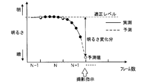
- FIG. 6 is a schematic diagram illustrating an example in which the calculation unit 240 predicts changes in brightness of an image based on signals from pixels 10 having photoelectric conversion units for image generation included in the region of interest T1.
- the horizontal axis indicates the number of frames of the live view image, and the vertical axis indicates the brightness of the image.
- the partial image in the region of interest T1 is read out at high speed equivalent to 150 fps, which is five times the live view image.
- An image in the region of interest T1 is called a partial image.
- the white circles in FIG. 6 indicate the readout timing of the live view image. It is assumed that the live view image includes the most recently read N frames and the previous N ⁇ 1 frames. Also, the black circles in FIG. 6 indicate the readout timing of the partial image in the region of interest T1. Five frames of partial images are read out while one frame of the live view image is read out.
- the calculation unit 240 calculates the average value of the digital signals forming the partial image, and uses the calculated average value as the brightness information of the partial image.
- the average value of the digital signals forming the partial image can be calculated five times while the live view image of one frame is being read.
- the brightness of the partial image gradually decreases during the shooting of the live view image of the N+1th frame.
- the calculation unit 240 extrapolates the brightness at the read timing of the live view image of the N+1th frame based on the amount of temporal change in the brightness of the partial image.
- the predicted value calculated by the calculator 240 is used by the in-sensor controller 260 as follows.
- the in-sensor control unit 260 calculates the amount of change in brightness at the readout timing of the N+1th frame live view image predicted by the calculation unit 240 (the brightness at the readout timing of the Nth frame and the predicted value at the readout timing of the N+1th frame ), the amplification gain for the signals of all the pixels 10 included in the imaging range 50 is increased, or the signal of all the pixels 10 included in the imaging range 50 is increased or Setting processing based on the information indicating the brightness of the image is performed by, for example, lengthening the photoelectric conversion time of 10 .
- the in-sensor control unit 260 detects the change in brightness at the readout timing of the N+1th frame live view image predicted by the calculation unit 240.
- the amplification gain for the signals of all the pixels 10 included in the shooting range 50 is lowered, or the photoelectric conversion of all the pixels 10 included in the shooting range 50 is reduced.
- Setting processing is performed based on the information indicating the brightness of the image, such as by shortening the conversion time.
- At least one of the amplification gain and the photoelectric conversion time at the time of photographing is set.
- the in-sensor control unit 260 performs at least one of setting the gain for the amplification unit 220 and setting the photoelectric conversion time for the pixels 10 based on the information indicating the brightness of the image calculated by the calculation unit 240 . Since it is configured in this way, feedback control can be performed within the imaging element 3 to bring the brightness of the image closer to an appropriate level, for example. Therefore, the amount of data and the like to be transmitted between the imaging element 3 and the external circuit or the like can be reduced.
- the calculation unit 240 of the image sensor 3 outputs, for example, from the pixel 10 having a photoelectric conversion unit for focus detection included in the region of interest T2, and outputs the A/D conversion unit Information indicating the intensity distribution of the signals from the focus detection pixels is calculated based on the digital signals converted in 230 .
- the information calculated by the calculation unit 240 is transmitted to the control unit 4 via the output unit 270 and used to determine the validity of focus adjustment.
- Information indicating the region of interest T ⁇ b>2 set by the control unit 4 is transmitted to the image sensor 3 via the image processing engine 30 .
- FIG. 7 is a diagram illustrating the intensity distribution of a pair of subject images generated by the above-described pair of light beams for focus detection.
- the horizontal axis indicates the position in the X-axis direction of the pixels 10 in which the photoelectric conversion units for focus detection are arranged, and the vertical axis indicates the signal value of the digital signal.
- the above-mentioned pair of light beams are A and B
- the image generated by the light beam A is represented by the curve 71
- the image generated by the light beam B is represented by the curve 72.
- the curve 72 is a curve based on the signal values read from the pixels 10 receiving the luminous flux B.
- the partial image in the region of interest T2 is read at high speed equivalent to 150 fps, which is five times the live view image.
- the calculation unit 240 calculates the difference between the average value of the digital signal values indicating the intensity distribution of the subject image indicated by the curve 71 and the average value of the digital signal values indicating the intensity distribution of the subject image indicated by the curve 72. Calculate That is, while one frame of the live view image for monitor display is being read out, the difference between the average values based on the signals of the partial images can be calculated five times.
- the difference between the average values calculated by the calculation unit 240 is sent to the image processing engine 30 (that is, the control unit 4) as information indicating the focus adjustment state of the imaging optical system 2.
- the difference between the average values calculated by the calculator 240 is used by the controller 4 as follows.
- the control unit 4 determines the validity of the focus adjustment based on the information calculated by the calculation unit 240 of the imaging device 3.
- the example of FIG. 7 is an example in which the signal value indicated by the curve 72 is lower than the signal value indicated by the curve 71 by an allowance or more due to the difference in the amount of light between the light beams A and B for focus detection. In this way, when the curve 71 and the curve 72 based on a pair of light beams A and B with a low degree of coincidence, in which there is a difference greater than the allowable difference between the curves 71 and 72, a pair of It becomes difficult to accurately calculate the image shift amount of the image of the subject.
- the control unit 4 determines whether the focus adjustment is appropriate. It is determined that the lens is missing, and the focus detection unit 41 is not caused to generate a control signal for moving the focusing lens of the photographing optical system 2 .
- the adequacy of focus adjustment can be judged in a short period of time while one frame of live view image is being photographed, and useless driving of the focusing lens can be avoided when the adequacy is lacking.
- the control unit 4 determines the validity of focus adjustment based on the intensity distribution of the images of the two subjects based on the light beams A and B.
- the validity of the focus adjustment may be determined based on whether or not the peak value of the intensity distribution of the image exceeds a predetermined determination threshold.
- the calculator 240 in this case calculates the peak value of the intensity distribution of the subject image indicated by the curve 71 or curve 72 .
- the peak value of the intensity distribution of the object image calculated by the calculation unit 240 is sent to the image processing engine 30 (that is, the control unit 4) as information indicating the focus adjustment state of the imaging optical system 2.
- control unit 4 determines that the focus adjustment lacks validity, and causes the focus detection unit 41 to move the focusing lens of the photographic optical system 2. Do not generate control signals for
- the control unit 4 determines that the peak coordinates of the intensity distribution of the image of the subject in row A or row B (in other words, the position in the X-axis direction of the pixels 10 in which the photoelectric conversion units for focus detection are arranged)
- the validity of the focus adjustment may be determined based on whether or not it is within a predetermined range from the center of the range 50 .
- the calculator 240 in this case calculates the peak coordinates of the intensity distribution of the subject image indicated by the curve 71 or curve 72 .
- the peak coordinates calculated by the calculation unit 240 are sent to the image processing engine 30 (that is, the control unit 4) via the output unit 270 as information indicating the state of focus adjustment of the imaging optical system 2.
- FIG. When the peak coordinate of the intensity distribution of the image of the subject is not included in the predetermined range from the center of the photographing range 50, the control unit 4 determines that the focus adjustment lacks validity. do not generate a control signal to move the focusing lens.
- control unit 4 determines the validity of the focus adjustment based on whether or not the variation width of the intensity distribution of the image of the subject in row A or row B is less than a predetermined value (in other words, the contrast of the image is insufficient). It may be configured to determine The calculation unit 240 in this case calculates the variation width based on the intensity distribution of the subject image indicated by the curve 71 or curve 72 . The variation width calculated by the calculation unit 240 is sent to the image processing engine 30 (that is, the control unit 4) via the output unit 270 as information indicating the focus adjustment state of the imaging optical system 2. FIG. The control unit 4 determines that the focus adjustment is not appropriate when the variation width of the intensity distribution of the image of the object is less than a predetermined value, and instructs the focus detection unit 41 to move the focusing lens of the photographing optical system 2. Do not generate control signals.
- the photoelectric conversion time of the partial image is the photoelectric conversion time of the live view image. (eg 1/5) compared to . Therefore, when the amplification gain for the signal is set to the same extent for the live-view image and the partial image, the signal level of the partial image per frame is smaller than the signal level of the live-view image (for example, 1 /5).
- the calculation unit 240 of the embodiment performs complementary processing so that the signal level of the partial image of the region of interest T1 approaches the signal level of the live view image. For example, with respect to the digital signal from the region of interest T1, digital signals of partial images of 5 frames read out at a higher frame rate (for example, 5 times) than the live view image are added for each pixel 10, and the gain is adjusted as necessary. After adjustment, it is embedded in the region of interest T1 in the live-view image and complemented as one live-view image.
- FIG. 8(a) is a diagram illustrating an imaging range 50 and a region of interest T1 imaged by the imaging device 3.
- FIG. 8B is a schematic diagram illustrating photoelectric conversion times for a partial image shot in the region of interest T1 and a live view image shot outside the region of interest T1.
- FIG. 8B illustrates a case where five frames of partial images are read from the region of interest T1 while one frame of the live view image is read.
- the memory 250 stores a digital signal based on the pixels 10 corresponding to the entire shooting range 50 captured by the image sensor 3 and a part of the shooting range 50 (region of interest T1 or T2) based on the pixel 10 can be stored.
- the memory 250 has a storage capacity capable of storing at least a plurality of frames (for example, 20 frames) of partial images and at least one frame of the entire image. Since the number of signals forming the partial image is smaller than the number of signals forming the entire image of the photographing range 50, the storage capacity of the memory 250 can be reduced compared to the case of storing a plurality of frames of the entire image.
- the calculation unit 240 adds partial images of a plurality of frames captured in the region of interest T1 at a frame rate higher than that of the live view image, and uses the signals of the partial images after the addition to obtain images of regions other than the region of interest T1. Complement the live view image taken in the area. Since it is configured in this way, it is possible to perform complementing processing of the live view image within the imaging device 3 .
- the image sensor 3 detects the brightness of an image based on signals output from a plurality of pixels 10 that output signals based on photoelectrically converted charges and a region of interest T1 that is a part of the plurality of pixels 10. and at least one of the information used to determine the appropriateness of focus adjustment as an evaluation value; and an in-sensor controller 260 that controls at least one of the photoelectric conversion time and the amplification gain for the signal in the pixels 10 of the region of interest T1.
- the image pickup device 3 compared to the case where the signal photoelectrically converted by the image pickup device 3 is output to the outside of the image pickup device 3 and the evaluation value is calculated by an external image processing engine 30 or the like, the image pickup device 3 The number of data output to the image processing engine 30 can be reduced. As a result, the processing time for the image sensor 3 to output data and the power consumption in the image sensor 3 can be reduced. In addition, feedback control of at least one of photoelectric conversion time and amplification gain for the pixels 10 of the image pickup device 3 can be performed inside the image pickup device 3 .
- the signal photoelectrically converted by the image sensor 3 is output to the outside of the image sensor 3, an evaluation value is calculated by an external image processing engine 30 or the like, and feedback control of the photoelectric conversion time or amplification gain is performed based on this evaluation value. is performed from the outside of the imaging device 3, at least the time required for transmitting and receiving data can be omitted, so feedback control can be performed in a short time.
- the calculation unit 240 of the imaging device 3 extrapolates the evaluation value based on the temporal change in the calculated evaluation value. With this configuration, it becomes possible to appropriately control the photoelectric conversion time or the amplification gain of the pixels 10 when capturing a live view image of the next frame, for example.
- the signals output from the pixels 10 of the image sensor 3 are a first signal as a live view image output from all of the plurality of pixels 10 for monitor display, and a plurality of pixels 10 for calculating evaluation values.
- the calculation unit 240 calculates an evaluation value based on the second signal. With this configuration, the calculation unit 240 can appropriately calculate the evaluation value using the second signal that is output separately from the first signal that is output for monitor display.
- the frame rate at which the second signal is output from the pixels 10 of the imaging element 3 is higher than the frame rate at which the first signal is output.
- the calculation unit 240 can calculate the evaluation value based on the second signal five times while the live view image (first signal) for monitor display of one frame is read. Therefore, it is possible to appropriately control the photoelectric conversion time or amplification gain for the live view image of the next frame based on the five calculated evaluation values.
- the calculation unit 240 of the image pickup device 3 adds, for example, five frames of the second signals forming the partial images output from the pixels 10 of the region of interest T1, and uses the added signals to calculate the pixels 10 of the region of interest T1. Complement the first signal corresponding to the position. Since it is configured in this way, the live view image complementing process can be appropriately performed within the imaging device 3 .
- the imaging device 1 determines the validity of the focus adjustment of the photographic optical system 2 based on the image sensor 3 and the information output from the image sensor 3 and used as an evaluation value for determining the validity of the focus adjustment.
- a control unit 4 is provided.
- the calculation unit 240 can calculate the information used to determine the validity of focus adjustment five times while one frame of the live view image for monitor display is being read. Therefore, compared to the case where the focus detection unit 41 of the control unit 4 performs the focus detection calculation using the signals of the focus detection pixels transmitted from the image sensor 3 at the same timing as the signals of the live view image, the speed is five times faster. It is possible to judge the adequacy of focus adjustment at a low level.
- the imaging element 3 is configured as a backside illumination type.
- the imaging element 3 may have a surface-illuminated configuration in which the wiring layer 140 is provided on the light incident surface side.
- Modification 2 In the embodiment described above, an example using a photodiode as a photoelectric conversion unit has been described. However, a photoelectric conversion film may be used as the photoelectric conversion portion.
- the imaging device 3 may be applied to a camera, a smartphone, a tablet, a camera built into a PC, an in-vehicle camera, and the like.
- the in-sensor control unit 260 controls at least one of the gain setting for the amplification unit 220 and the photoelectric conversion time setting for the pixels 10 based on the information indicating the brightness of the image calculated by the calculation unit 240.
- the information indicating the brightness of the image calculated by the calculation unit 240 is sent to the control unit 4, and the exposure control unit 42 of the control unit 4 performs exposure calculation based on the information indicating the brightness of the image, and controls the exposure.
- the section 4 may be configured to control the aperture driving section 8 based on the exposure calculation result.
- the information indicating the brightness of the image calculated by the calculator 240 is sent to the image processing engine 30 (that is, the controller 4) via the output unit 270.
- the exposure control unit 42 of the control unit 4 performs exposure calculations based on the information sent from the image sensor 3, and controls the aperture value, shutter speed, and sensitivity described above.
- the exposure control section 42 and the aperture driving section 8 may be collectively referred to as a light amount adjusting section 9 (FIG. 5) for adjusting the amount of light incident on the image pickup device 3 .
- the calculation unit 240 can calculate the information indicating the brightness of the image five times while one frame of the live view image for monitor display is being read. Therefore, when the exposure control unit 42 of the control unit 4 performs the exposure calculation using the information indicating the brightness of the image calculated by the calculation unit 240, the signal of the live view image sent from the image pickup device 3 is used for exposure. Exposure calculation can be performed at a speed five times faster than when calculation is performed, and followability to changes in image brightness can be enhanced. In Modified Example 4, the number of times the information indicating the brightness of the image calculated by the calculation unit 240 is sent to the image processing engine 30 (that is, the control unit 4) increases. Since the number of signals of the information indicating the brightness of is sufficiently small compared to the signals forming the live view image, the amount of data sent from the imaging device 3 to the control unit 4 does not increase significantly.
- the information indicating the intensity distribution of the pair of subject images generated by the pair of light beams for focus detection calculated by the calculator 240 is sent to the image processing engine 30 (that is, the control 4).
- a focus detection unit 41 of the control unit 4 performs focus detection calculation based on information sent from the image sensor 3 and sends a control signal for moving the focusing lens to the lens driving unit 7 .
- the calculation unit 240 can calculate the intensity distribution of the pair of subject images five times while one frame of the live view image for monitor display is read. Therefore, when the focus detection unit 41 of the control unit 4 performs focus detection calculation using the information indicating the intensity distribution of the images of the pair of subjects calculated by the calculation unit 240, the signal from the image sensor 3 is the same as the signal of the live view image. Computation can be performed at a speed five times faster than when focus detection computation is performed using the signals of the focus detection pixels transmitted at the timing, and tracking to changes in subject distance can be enhanced.
- the present invention is not limited to the contents of the embodiments and modifications.
- the scope of the present invention also includes a mode in which each configuration shown in the embodiment and modifications is used in combination.
- Other aspects conceivable within the scope of the technical idea of the present invention are also included in the scope of the present invention.
Landscapes
- Engineering & Computer Science (AREA)
- Multimedia (AREA)
- Signal Processing (AREA)
- Transforming Light Signals Into Electric Signals (AREA)
- Studio Devices (AREA)
Abstract
撮像素子は、光電変換された電荷に基づく信号を出力する複数の画素を有する第1基板と、前記複数の画素のうち、少なくとも第1画素から出力された第1信号と、前記第1画素から、前記第1信号の後に出力された第2信号とをデジタル信号に変換する変換部を有する第2基板と、前記変換部でデジタル信号に変換された前記第1信号に基づく評価値の算出と、前記変換部でデジタル信号に変換された前記第1信号と、前記変換部でデジタル信号に変換された前記第2信号とに基づく画像信号の生成とを行う算出部を有する第3基板と、を備える。
Description
本発明は、撮像素子および撮像装置に関する。
本願は、2021年5月24日に出願された日本国特願2021-087030号に基づき優先権を主張し、その内容をここに援用する。
本願は、2021年5月24日に出願された日本国特願2021-087030号に基づき優先権を主張し、その内容をここに援用する。
イメージセンサで撮像された画像のデータは、画像処理エンジンと呼ばれる外部の回路等へ読み出され、信号処理等に用いられる。イメージセンサから外部の回路等へ送出する画像のデータが多くなるほど、イメージセンサからデータを出力する処理の時間が長くなってしまう。
本発明に係る第1の態様による撮像素子は、光電変換された電荷に基づく信号を出力する複数の画素を有する第1基板と、前記複数の画素のうち、少なくとも第1画素から出力された第1信号と、前記第1画素から、前記第1信号の後に出力された第2信号とをデジタル信号に変換する変換部を有する第2基板と、前記変換部でデジタル信号に変換された前記第1信号に基づく評価値の算出と、前記変換部でデジタル信号に変換された前記第1信号と、前記変換部でデジタル信号に変換された前記第2信号とに基づく画像信号の生成とを行う算出部を有する第3基板と、を備える。
本発明に係る第2の態様による撮像装置は、第1の態様による撮像素子を備える。
本発明に係る第2の態様による撮像装置は、第1の態様による撮像素子を備える。
以下、図面を参照して発明を実施するための形態について説明する。
<撮像装置の構成>
図1は、実施の形態に係る撮像素子3を搭載する撮像装置1の構成を例示するブロック図である。撮像装置1は、撮影光学系2(21)、撮像素子3、制御部4、レンズ駆動部7および絞り駆動部8を備え、メモリカード等の記憶媒体5が装脱可能に構成される。撮像装置1は、例えばカメラである。撮影光学系2は、複数のレンズおよび絞り21を有し、撮像素子3上に被写体像を結像する。撮像素子3は、撮影光学系2により結像される被写体像を撮像して画像信号を生成する。撮像素子3は、例えばCMOSイメージセンサである。
<撮像装置の構成>
図1は、実施の形態に係る撮像素子3を搭載する撮像装置1の構成を例示するブロック図である。撮像装置1は、撮影光学系2(21)、撮像素子3、制御部4、レンズ駆動部7および絞り駆動部8を備え、メモリカード等の記憶媒体5が装脱可能に構成される。撮像装置1は、例えばカメラである。撮影光学系2は、複数のレンズおよび絞り21を有し、撮像素子3上に被写体像を結像する。撮像素子3は、撮影光学系2により結像される被写体像を撮像して画像信号を生成する。撮像素子3は、例えばCMOSイメージセンサである。
制御部4は、撮像素子3の動作を制御するための制御信号を撮像素子3に出力する。制御部4はさらに、撮像素子3から出力された画像信号に対して各種の画像処理を施し、画像データを生成する画像生成部として機能する。また、制御部4は、図5を参照して後述する焦点検出部41および露出制御部42を含む。レンズ駆動部7は、制御部4(焦点検出部41)からの制御信号に基づき、主要被写体にピントを合わせるために撮影光学系2を構成するフォーカシングレンズを光軸Axの方向に移動させる。絞り駆動部8は、制御部4(露出制御部42)からの制御信号に基づき、絞り21の開口径を調節し、撮像素子3に入射する光量を調節する。記憶媒体5には、制御部4で生成された画像データが所定のファイル形式で記録される。
なお、撮影光学系2は、撮像装置1から着脱可能に構成してもよい。
なお、撮影光学系2は、撮像装置1から着脱可能に構成してもよい。
<撮像素子の断面構造>
図2は、図1の撮像素子3の断面構造を例示する図である。図2に示す撮像素子3は、裏面照射型の撮像素子である。撮像素子3は、第1基板111と、第2基板112と、第3基板113と、第4基板114とを備える。第1基板111、第2基板112、第3基板113および第4基板114は、それぞれ半導体基板等により構成される。第1基板111は、配線層140と配線層141を介して第2基板112に積層される。第2基板112は、配線層142と配線層143を介して第3基板113に積層される。第3基板113は、配線層144と配線層145を介して第4基板114に積層される。
図2は、図1の撮像素子3の断面構造を例示する図である。図2に示す撮像素子3は、裏面照射型の撮像素子である。撮像素子3は、第1基板111と、第2基板112と、第3基板113と、第4基板114とを備える。第1基板111、第2基板112、第3基板113および第4基板114は、それぞれ半導体基板等により構成される。第1基板111は、配線層140と配線層141を介して第2基板112に積層される。第2基板112は、配線層142と配線層143を介して第3基板113に積層される。第3基板113は、配線層144と配線層145を介して第4基板114に積層される。
白抜き矢印で示す入射光Lは、Z軸プラス方向へ向かって入射する。また、座標軸に示すように、Z軸に直交する紙面右方向をX軸プラス方向、Z軸およびX軸に直交する紙面手前方向をY軸プラス方向とする。撮像素子3は、入射光Lが入射する方向に、第1基板111と第2基板112と第3基板113と第4基板114とが積層されている。
撮像素子3はさらに、マイクロレンズ層101、カラーフィルタ層102、パッシベーション層103を有する。これらのパッシベーション層103、カラーフィルタ層102およびマイクロレンズ層101は、第1基板111に順次積層されている。
マイクロレンズ層101は、複数のマイクロレンズMLを有する。マイクロレンズMLは、入射した光を後述する光電変換部に集光する。カラーフィルタ層102は、複数のカラーフィルタFを有する。パッシベーション層103は、窒化膜や酸化膜で構成される。
マイクロレンズ層101は、複数のマイクロレンズMLを有する。マイクロレンズMLは、入射した光を後述する光電変換部に集光する。カラーフィルタ層102は、複数のカラーフィルタFを有する。パッシベーション層103は、窒化膜や酸化膜で構成される。
第1基板111、第2基板112、第3基板113、および第4基板114は、それぞれゲート電極やゲート絶縁膜が設けられる第1面105a、106a、107a、108aと、第1面とは異なる第2面105b、106b、107b、108bとを有する。また、第1面105a、106a、107a、108aには、それぞれトランジスタ等の各種素子が設けられる。第1基板111の第1面105a、第2基板112の第1面106a、第3基板113の第1面107a、および第4基板114の第1面108aには、それぞれ配線層140、141、144、145が積層して設けられる。また、第2基板112の第2面106bおよび第3基板113の第2面107bには、それぞれ配線層(基板間接続層)142、143が積層して設けられる。配線層140~配線層145は、導体膜(金属膜)および絶縁膜を含む層であり、それぞれ複数の配線やビアなどが配置される。
第1基板111の第1面105aの素子および第2基板112の第1面106aの素子は、配線層140、141を介してバンプや電極等の接続部109により電気的に接続される。同様に第3基板113の第1面107aの素子および第4基板114の第1面108aの素子は、配線層144、145を介してバンプや電極等の接続部109により電気的に接続される。また、第2基板112および第3基板113は、複数の貫通電極110を有する。第2基板112の貫通電極110は、第2基板112の第1面106aおよび第2面106bに設けられた回路を互いに接続し、第3基板113の貫通電極110は、第3基板113の第1面107aおよび第2面107bに設けられた回路を互いに接続する。第2基板112の第2面106bに設けられた回路および第3基板113の第2面107bに設けられた回路は、基板間接続層142、143を介してバンプや電極等の接続部109により電気的に接続される。
なお、実施の形態では第1基板111、第2基板112、第3基板113、および第4基板114が積層される場合を例示するが、積層される基板の数は、実施の形態より多くても少なくてもよい。
また、第1基板111、第2基板112、第3基板113、および第4基板114を、それぞれ第1層、第2層、第3層および第4層と称してもよい。
なお、実施の形態では第1基板111、第2基板112、第3基板113、および第4基板114が積層される場合を例示するが、積層される基板の数は、実施の形態より多くても少なくてもよい。
また、第1基板111、第2基板112、第3基板113、および第4基板114を、それぞれ第1層、第2層、第3層および第4層と称してもよい。
<撮像素子の構成例>
図3は、実施の形態に係る撮像素子3における第1基板111~第4基板114の各層の構成を例示するブロック図である。第1基板111は、例えば、2次元状に配置される複数の画素10と、信号の読出部20とを有する。配列された複数の画素10および読出部20を、画素アレイ210と呼んでもよい。画素10は、図2に示すX軸方向(行方向)およびY軸方向(列方向)に並べて配置されている。画素10は、フォトダイオード(PD)等の光電変換部を有し、入射光Lを電荷に変換する。読出部20は、画素10ごとに設けられ、対応する画素10で光電変換された電荷に基づく信号(光電変換信号)を読み出す。読出部20が画素10から信号を読み出すために必要な読出制御信号は、第2基板112のセンサ内制御部260から読出部20へ供給される。読出部20により読み出された信号は、第2基板112へ送出される。
図3は、実施の形態に係る撮像素子3における第1基板111~第4基板114の各層の構成を例示するブロック図である。第1基板111は、例えば、2次元状に配置される複数の画素10と、信号の読出部20とを有する。配列された複数の画素10および読出部20を、画素アレイ210と呼んでもよい。画素10は、図2に示すX軸方向(行方向)およびY軸方向(列方向)に並べて配置されている。画素10は、フォトダイオード(PD)等の光電変換部を有し、入射光Lを電荷に変換する。読出部20は、画素10ごとに設けられ、対応する画素10で光電変換された電荷に基づく信号(光電変換信号)を読み出す。読出部20が画素10から信号を読み出すために必要な読出制御信号は、第2基板112のセンサ内制御部260から読出部20へ供給される。読出部20により読み出された信号は、第2基板112へ送出される。
第2基板112は、例えば、A/D変換部230と、センサ内制御部260とを有する。A/D変換部230は、対応する画素10から出力される信号をデジタル信号に変換する。A/D変換部230で変換された信号は、第3基板113へ送出される。
センサ内制御部260は、第4基板114の入力部290を介して入力される指示信号に基づき、読出部20に対する読出制御信号を生成する。指示信号は、図5を参照して後述する画像処理エンジン30から送出される。センサ内制御部260で生成された読出制御信号は、第1基板111へ送出される。
センサ内制御部260は、第4基板114の入力部290を介して入力される指示信号に基づき、読出部20に対する読出制御信号を生成する。指示信号は、図5を参照して後述する画像処理エンジン30から送出される。センサ内制御部260で生成された読出制御信号は、第1基板111へ送出される。
第3基板113は、例えば、メモリ250と、算出部240と、を有する。メモリ250は、A/D変換部230で変換されたデジタル信号を記憶する。算出部240は、メモリ250に記憶されているデジタル信号、および前記A/D変換部230で変換されたデジタル信号の少なくとも一方のデジタル信号を用いて所定の演算を行う。演算には、以下に例示する演算の少なくとも一つが含まれる。
(1)撮像素子3で撮像される画像の明るさを示す情報を算出すること
(2)撮影光学系2のフォーカス調節の状態を示す情報を算出すること
(3)ライブビュー画像における補完処理を行うこと
ライブビュー画像は、A/D変換部230で変換されたデジタル信号に基づいて生成されるモニタ表示用の画像であり、スルー画とも称される。
(1)撮像素子3で撮像される画像の明るさを示す情報を算出すること
(2)撮影光学系2のフォーカス調節の状態を示す情報を算出すること
(3)ライブビュー画像における補完処理を行うこと
ライブビュー画像は、A/D変換部230で変換されたデジタル信号に基づいて生成されるモニタ表示用の画像であり、スルー画とも称される。
第4基板114は、例えば、出力部270と、入力部290とを有する。出力部270は、メモリ250に記憶されているデジタル信号、上記A/D変換部230で変換されたデジタル信号、または、算出部240の演算結果を示す情報を、後述する画像処理エンジン30(図5)へ送出する。
入力部290には、画像処理エンジン30からの指示信号が入力される。指示信号は、第2基板112へ送られる。
入力部290には、画像処理エンジン30からの指示信号が入力される。指示信号は、第2基板112へ送られる。
<フォーカスポイント>
フォーカスポイントおよび着目領域について説明する。撮像素子3の画素アレイ210を構成する画素10は、画像生成用の光電変換部を有する。ただし、フォーカスポイントに対応する領域の一部または全部には、画像生成用の光電変換部の代わりに焦点検出用の光電変換部を有する画素10が配置される。図4は、撮像素子3によって撮像される撮影範囲50を説明する図である。撮影範囲50には、あらかじめ複数のフォーカスポイントPが設けられている。フォーカスポイントPは、撮影範囲50において撮影光学系2のフォーカス調節が可能な位置を示し、焦点検出エリア、焦点検出位置、測距点とも称される。図4では、フォーカスポイントPを示す四角形のマークを、ライブビュー画像に重ねて例示する。
なお、図示したフォーカスポイントPの数と撮影範囲50における位置は一例に過ぎず、図4の態様に限定されるものではない。
制御部4(焦点検出部41)は、焦点検出用の光電変換部を有する画素10からの光電変換信号に基づき、撮影光学系2の異なる領域を通過する一対の光束による一対の像の像ずれ量(位相差)を算出する。像ずれ量の算出は、フォーカスポイントPごとに算出することができる。
上記一対の像の像ずれ量は、撮影光学系2を通過した光束により形成される被写体の像の位置と、撮像素子3の撮像面の位置とのずれ量であるデフォーカス量の算出の元になる値であり、上記一対の像の像ずれ量に所定の変換係数をかけることによってデフォーカス量を算出することができる。
上記一対の像の像ずれ量は、撮影光学系2を通過した光束により形成される被写体の像の位置と、撮像素子3の撮像面の位置とのずれ量であるデフォーカス量の算出の元になる値であり、上記一対の像の像ずれ量に所定の変換係数をかけることによってデフォーカス量を算出することができる。
制御部4(焦点検出部41)はさらに、例えば、複数のフォーカスポイントPのうちの撮像装置1から最も近い被写体に対応するフォーカスポイントPで算出された上記一対の像の像ずれ量に基づき、撮影光学系2のフォーカシングレンズを移動させるための制御信号を生成する。
なお、制御部4(焦点検出部41)は、全てのフォーカスポイントPの中から上記一対の像の像ずれ量の算出(換言すると、デフォーカス量の算出)に用いるフォーカスポイントPを自動で選ぶことも、ユーザが後述する操作部材6を操作することによって指示するフォーカスポイントPを選ぶこともできる。
なお、制御部4(焦点検出部41)は、全てのフォーカスポイントPの中から上記一対の像の像ずれ量の算出(換言すると、デフォーカス量の算出)に用いるフォーカスポイントPを自動で選ぶことも、ユーザが後述する操作部材6を操作することによって指示するフォーカスポイントPを選ぶこともできる。
<着目領域>
図4には、着目領域T1およびT2を示す枠も例示する。破線で囲む着目領域T1は、制御部4によって設定される。制御部4(露出制御部42)は、主要被写体(例えば人物の顔)を含む位置に着目領域T1を設定し、着目領域T1に含まれる画像生成用の画素10からの信号を用いて被写体の明るさ情報(Bv値)を検出する。制御部4(露出制御部42)は、例えばBv値およびプログラム線図の情報に基づいて、絞り値(Av値)、シャッター速度(Tv値)、および感度(Sv値)を決定する。
制御部4は、ライブビュー画像のデータに基づいて行われる公知の画像認識処理で検出された人物等の位置、または、ユーザが後述する操作部材6を操作することによって入力された位置を、撮影範囲50における主要被写体の位置とすることができる。なお、撮影範囲50の全部を着目領域T1にしてもよい。
実線で囲む着目領域T2も、制御部4によって設定される。制御部4(焦点検出部41)は、例えば、人物の眼を含む行方向(図2に示すX軸方向)に着目領域T2を設定し、着目領域T2に含まれる焦点検出用の画素10からの信号を用いて上記一対の像の像ずれ量(位相差)を算出することができる。
実施の形態による画素アレイ210を構成する画素10では、画素10ごとに電荷蓄積時間を制御することができる。換言すると、各画素10は、異なったフレームレートで撮影した信号をそれぞれ出力させることができる。具体的には、ある画素10で1回の電荷蓄積を行わせている間に、他の画素10に複数回の電荷蓄積を行わせることにより、それぞれの画素10から異なるフレームレートで信号を読出すことが可能に構成されている。
また、実施の形態では、画素10から出力される信号に対する増幅利得を画素10ごとに制御することができる。例えば、各画素10で電荷蓄積時間を異ならせて撮影するなどして、各画素10から読出された信号レベルが異なる場合に、信号レベルを揃えるように増幅利得を設定することが可能に構成されている。
<撮像素子と画像処理エンジン>
図5は、実施の形態に係る撮像素子3と、画像処理エンジン30との間のデータ等の受け渡しを説明する模式図である。
撮像素子3は、画像処理エンジン30から記録用の撮影の指示信号が入力されると、記録用の画像の撮像を行い、撮像した画像のデータを記録用画像のデータとして画像処理エンジン30へ送出する。記録用画像のデータを画像処理エンジン30へ送出する場合、例えば、メモリ250に記憶されているデジタル信号を記録用画像のデータとして送出することができる。
図5は、実施の形態に係る撮像素子3と、画像処理エンジン30との間のデータ等の受け渡しを説明する模式図である。
撮像素子3は、画像処理エンジン30から記録用の撮影の指示信号が入力されると、記録用の画像の撮像を行い、撮像した画像のデータを記録用画像のデータとして画像処理エンジン30へ送出する。記録用画像のデータを画像処理エンジン30へ送出する場合、例えば、メモリ250に記憶されているデジタル信号を記録用画像のデータとして送出することができる。
撮像素子3は、画像処理エンジン30からモニタ表示用の撮影の指示信号が入力されると、複数フレームのモニタ表示用の画像の撮像を行い、撮像した画像のデータをライブビュー画像のデータとして画像処理エンジン30へ送出する。ライブビュー画像のデータを画像処理エンジン30へ送出する場合、例えば、A/D変換部230で変換されたデジタル信号をライブビュー画像のデータとして送出することができる。
撮像素子3は、画像のデータ以外にも算出部240の演算結果を示す情報を画像処理エンジン30へ送出することが可能に構成されている。
<画像処理エンジン>
実施の形態では、画像処理エンジン30は制御部4に含まれている。画像処理エンジン30は、撮像素子制御部310と、入力部320と、画像処理部330と、メモリ340とを有する。
レリーズボタンや操作スイッチ等を含む操作部材6は、例えば、撮像装置1の外装面に設けられている。操作部材6は、ユーザの操作に応じた操作信号を撮像素子制御部310へ送出する。ユーザは、操作部材6を操作することにより、撮像装置1に対する撮影指示や撮影条件等の設定指示を行う。
実施の形態では、画像処理エンジン30は制御部4に含まれている。画像処理エンジン30は、撮像素子制御部310と、入力部320と、画像処理部330と、メモリ340とを有する。
レリーズボタンや操作スイッチ等を含む操作部材6は、例えば、撮像装置1の外装面に設けられている。操作部材6は、ユーザの操作に応じた操作信号を撮像素子制御部310へ送出する。ユーザは、操作部材6を操作することにより、撮像装置1に対する撮影指示や撮影条件等の設定指示を行う。
撮像素子制御部310は、撮影条件等の設定指示が行われると、設定された撮影条件を示す情報を撮像素子3へ送出する。また、撮像素子制御部310は、レリーズボタンが全押し操作時のストロークよりも短いストロークで半押し操作されたことを示す半押し操作信号が操作部材6から入力されると、不図示の表示部またはビューファインダーで連続的にモニタ表示用の画像を表示させるため、モニタ表示用の撮影開始を指示する指示信号を、撮像素子3へ送出する。
さらにまた、撮像素子制御部310は、レリーズボタンが半押し操作時よりも長いストロークで全押し操作されたことを示す全押し操作信号が操作部材6から入力されると、記録用の静止画の撮影開始を指示する指示信号を、撮像素子3へ送出する。
さらにまた、撮像素子制御部310は、レリーズボタンが半押し操作時よりも長いストロークで全押し操作されたことを示す全押し操作信号が操作部材6から入力されると、記録用の静止画の撮影開始を指示する指示信号を、撮像素子3へ送出する。
入力部320には、撮像素子3から出力された上記デジタル信号等が入力される。入力部320に入力されたデジタル信号のうち、画像生成用の光電変換部を有する画素10からの信号に基づくデジタル信号は、画像処理部330へ送られる。画像処理部330は、撮像素子3から取得したデジタル信号に対して所定の画像処理を行って画像データを生成する。生成された記録用の画像データは、メモリ340に記録されたり、撮影後の確認画像の表示に用いられたりする。メモリ340に記録された画像データは、上記記憶媒体5に記録することができる。また、生成されたモニタ表示用の画像データは、ビューファインダー等での表示に用いられる。
入力部320に入力されたデジタル信号のうち、画像生成用の光電変換部を有する画素10からの信号に基づくライブビュー画像の信号は、露出制御部42にも送られて露出演算に用いられる。露出演算により、上述した絞り値、シャッター速度、および感度が決定される。
入力部320に入力されたデジタル信号のうち、画像生成用の光電変換部を有する画素10からの信号に基づくライブビュー画像の信号は、露出制御部42にも送られて露出演算に用いられる。露出演算により、上述した絞り値、シャッター速度、および感度が決定される。
入力部320に入力されたデジタル信号のうち、焦点検出用の光電変換部を有する画素10からの信号に基づくデジタル信号は、焦点検出部41へ送られて焦点検出演算に用いられる。焦点検出演算により、上述したデフォーカス量が算出される。
また、入力部320に入力された、撮影光学系2のフォーカス調節の状態を示す情報は、制御部4において焦点調節の妥当性判断に用いられる。
また、入力部320に入力された、撮影光学系2のフォーカス調節の状態を示す情報は、制御部4において焦点調節の妥当性判断に用いられる。
<撮像素子>
撮像素子3は、図3を参照して説明した画素アレイ210、A/D変換部230、算出部240、メモリ250、センサ内制御部260、入力部290および出力部270に加えて、増幅部220を有する。増幅部220は、図3の第1基板111に設けることができる。増幅部220は、画素10から出力される信号を増幅し、増幅後の信号をA/D変換部220へ送出する。
また、センサ内制御部260は、上述した読出部20に対する読出制御信号の生成に加えて、以下の設定処理を行う。
撮像素子3は、図3を参照して説明した画素アレイ210、A/D変換部230、算出部240、メモリ250、センサ内制御部260、入力部290および出力部270に加えて、増幅部220を有する。増幅部220は、図3の第1基板111に設けることができる。増幅部220は、画素10から出力される信号を増幅し、増幅後の信号をA/D変換部220へ送出する。
また、センサ内制御部260は、上述した読出部20に対する読出制御信号の生成に加えて、以下の設定処理を行う。
(1)センサ内制御部260は、後述する画像の明るさを示す情報に基づき、増幅部220に対して増幅利得を設定する。増幅利得の設定は画素10単位で可能であり、例えば、撮影範囲50に含まれる全ての画素10の信号に対する増幅利得を同じにしたり、上記着目領域T1またはT2に含まれる画素10の信号に対する増幅利得を他の画素10の信号に対する増幅利得と異ならせたりすることができる。
(2)センサ内制御部260は、後述する画像の明るさを示す情報に基づき、撮影範囲50の画素10に対して光電変換時間(換言すると蓄積時間)を設定する。光電変換時間の設定は画素10単位で可能であり、例えば、撮影範囲50に含まれる全ての画素10の光電変換時間を同じにしたり、上記着目領域T1またはT2に含まれる画素10の光電変換時間を他の画素10の光電変換時間と異ならせたりすることができる。
<算出部が行う処理>
算出部240は、以下の処理を行うことができる。
1.画像の明るさを示す情報の算出
撮像素子3の算出部240は、例えば、上記着目領域T1に含まれる画像生成用の光電変換部を有する画素10から出力され、A/D変換部230で変換されたデジタル信号に基づいて、画像の明るさを示す情報を算出する。算出部240で算出した情報はセンサ内制御部260へ送出され、上述した設定処理に用いられる。
なお、制御部4で設定された着目領域T1を示す情報は、画像処理エンジン30を介して撮像素子3へ伝えられる。
算出部240は、以下の処理を行うことができる。
1.画像の明るさを示す情報の算出
撮像素子3の算出部240は、例えば、上記着目領域T1に含まれる画像生成用の光電変換部を有する画素10から出力され、A/D変換部230で変換されたデジタル信号に基づいて、画像の明るさを示す情報を算出する。算出部240で算出した情報はセンサ内制御部260へ送出され、上述した設定処理に用いられる。
なお、制御部4で設定された着目領域T1を示す情報は、画像処理エンジン30を介して撮像素子3へ伝えられる。
図6は、着目領域T1に含まれる画像生成用の光電変換部を有する画素10からの信号に基づいて、算出部240が画像の明るさの変化を予測する例を説明する模式図である。横軸はライブビュー画像のフレーム数を示し、縦軸は画像の明るさを示す。実施の形態では、ライブビュー画像を毎秒30フレームのフレームレート(以後30fpsと呼ぶ)で読出しながら、着目領域T1における部分画像をライブビュー画像の5倍の150fps相当で高速読出しする。着目領域T1における画像を部分画像と呼ぶ。
図6の白丸はライブビュー画像の読出しタイミングを示す。ライブビュー画像は、直近に読出されたNフレームと、一つ前のN-1フレームとが読出されているものとする。また、図6の黒丸は着目領域T1における部分画像の読出しタイミングを示す。1フレームのライブビュー画像が読出される間に5フレームの部分画像が読出される。
算出部240は、例えば、部分画像を構成するデジタル信号の平均値を算出し、算出した平均値をその部分画像の明るさ情報とする。実施の形態では、1フレームのライブビュー画像が読出される間に、部分画像を構成するデジタル信号の平均値を5回算出することができる。図6の例では、N+1フレーム目のライブビュー画像の撮影中に部分画像の明るさが徐々に低下している。算出部240は、部分画像の明るさの時間的変化量に基づいて、N+1フレーム目のライブビュー画像の読出しタイミングにおける明るさを外挿法により予測する。
算出部240で算出された予測値は、センサ内制御部260で以下のように用いられる。
センサ内制御部260は、算出部240で予測されたN+1フレーム目のライブビュー画像の読出しタイミングにおける明るさの変化分(Nフレーム目の読出しタイミングにおける明るさと、N+1フレーム目の読出しタイミングにおける予測値との差)を補うために、N+1フレーム目のライブビュー画像の撮影中に、例えば撮影範囲50に含まれる全ての画素10の信号に対する増幅利得を高めたり、撮影範囲50に含まれる全ての画素10の光電変換時間を長くしたりするなどして、画像の明るさを示す情報に基づいた設定処理を行う。
センサ内制御部260は、算出部240で予測されたN+1フレーム目のライブビュー画像の読出しタイミングにおける明るさの変化分(Nフレーム目の読出しタイミングにおける明るさと、N+1フレーム目の読出しタイミングにおける予測値との差)を補うために、N+1フレーム目のライブビュー画像の撮影中に、例えば撮影範囲50に含まれる全ての画素10の信号に対する増幅利得を高めたり、撮影範囲50に含まれる全ての画素10の光電変換時間を長くしたりするなどして、画像の明るさを示す情報に基づいた設定処理を行う。
また、ライブビュー画像の撮影中に部分画像の明るさが上昇する場合には、センサ内制御部260は、算出部240で予測されたN+1フレーム目のライブビュー画像の読出しタイミングにおける明るさの変化分を補うために、N+1フレーム目のライブビュー画像の撮影中に、例えば撮影範囲50に含まれる全ての画素10の信号に対する増幅利得を下げたり、撮影範囲50に含まれる全ての画素10の光電変換時間を短くしたりするなどして、画像の明るさを示す情報に基づいた設定処理を行う。
図6において白抜き矢印で示すタイミングでユーザから撮影指示の操作が行われる場合も同様に、センサ内制御部260は、算出部240で予測された明るさの変化の影響を抑えるために記録用の撮影時の増幅利得および光電変換時間の少なくとも一方を設定する。
上述したように、センサ内制御部260は、算出部240で算出された画像の明るさを示す情報に基づき、増幅部220に対するゲイン設定および画素10に対する光電変換時間の設定の少なくとも一方を行う。このように構成したので、例えば画像の明るさを適正レベルに近づけるフィードバック制御を撮像素子3内で行うことができる。したがって、撮像素子3と外部の回路等との間で送信するデータ等を少なく抑えることができる。
2.焦点調節の妥当性判断に用いられる情報の算出
撮像素子3の算出部240は、例えば、上記着目領域T2に含まれる焦点検出用の光電変換部を有する画素10から出力され、A/D変換部230で変換されたデジタル信号に基づいて、焦点検出用画素からの信号の強度分布を示す情報を算出する。算出部240で算出した情報は出力部270を介して制御部4へ伝えられ、焦点調節の妥当性判断に用いられる。
なお、制御部4で設定された着目領域T2を示す情報は、画像処理エンジン30を介して撮像素子3へ伝えられる。
撮像素子3の算出部240は、例えば、上記着目領域T2に含まれる焦点検出用の光電変換部を有する画素10から出力され、A/D変換部230で変換されたデジタル信号に基づいて、焦点検出用画素からの信号の強度分布を示す情報を算出する。算出部240で算出した情報は出力部270を介して制御部4へ伝えられ、焦点調節の妥当性判断に用いられる。
なお、制御部4で設定された着目領域T2を示す情報は、画像処理エンジン30を介して撮像素子3へ伝えられる。
図7は、上述した焦点検出用の一対の光束により生成された一対の被写体の像の強度分布を例示する図である。横軸は焦点検出用の光電変換部が配列されている画素10のX軸方向の位置、縦軸はデジタル信号の信号値を示す。上述した一対の光束を光束Aおよび光束Bとし、光束Aにより生成される像を曲線71で表し、光束Bにより生成される像を曲線72で表わすものとする。つまり、曲線71は、光束Aを受光する画素10から読出された信号値に基づく曲線であり、曲線72は、光束Bを受光する画素10から読出された信号値に基づく曲線である。
実施の形態では、ライブビュー画像を30fpsで読出しながら、着目領域T2における部分画像をライブビュー画像の5倍の150fps相当で高速読出しする。算出部240は、例えば、曲線71で示される被写体の像の強度分布を示すデジタル信号値の平均値と、曲線72で示される被写体の像の強度分布を示すデジタル信号値の平均値との差を算出する。つまり、1フレームのモニタ表示用のライブビュー画像が読出される間に、部分画像の信号に基づく上記平均値の差を5回算出することができる。
算出部240で算出された平均値の差は、撮影光学系2のフォーカス調節の状態を示す情報として画像処理エンジン30(すなわち制御部4)へ送出される。算出部240で算出された平均値の差は、制御部4で以下のように用いられる。
制御部4は、撮像素子3の算出部240で算出された情報に基づいて焦点調節の妥当性を判断する。図7の例は、焦点検出用の光束Aおよび光束B間の光量差等によって、曲線72で示される信号値が曲線71で示される信号値よりも許容差以上に低くなった例である。このように曲線71および曲線72に許容差以上の差が存在する、換言すると一致度が低い一対の光束Aおよび光束Bに基づく曲線71および曲線72を用いて焦点検出演算処理を行うと、一対の被写体の像の像ずれ量を精度よく算出することが困難になる。
そのため、制御部4は、曲線71で示されるデジタル信号値の平均値と、曲線72で示されるデジタル信号値の平均値との差が所定の判定閾値を超えた場合に焦点調節の妥当性に欠けると判断し、焦点検出部41に撮影光学系2のフォーカシングレンズを移動させるための制御信号を生成させない。このように構成したので、1フレームのライブビュー画像が撮影されている間の短時間に焦点調節の妥当性を判断し、妥当性に欠ける場合はフォーカシングレンズの無駄な駆動を避けることができる。
なお、上記説明では、制御部4が、光束Aおよび光束Bに基づく2つの被写体の像の強度分布に基づいて焦点調節の妥当性を判断する例を説明したが、A列またはB列の被写体の像の強度分布のピーク値が所定の判定閾値を超えているか否かに基づいて焦点調節の妥当性を判断するように構成してもよい。
この場合の算出部240は、曲線71または曲線72で示される被写体の像の強度分布のピーク値を算出する。算出部240で算出された被写体の像の強度分布のピーク値は、撮影光学系2のフォーカス調節の状態を示す情報として画像処理エンジン30(すなわち制御部4)へ送出される。
制御部4は、被写体の像の強度分布のピーク値が所定の判定閾値よりも低い場合に焦点調節の妥当性に欠けると判断し、焦点検出部41に撮影光学系2のフォーカシングレンズを移動させるための制御信号を生成させない。
この場合の算出部240は、曲線71または曲線72で示される被写体の像の強度分布のピーク値を算出する。算出部240で算出された被写体の像の強度分布のピーク値は、撮影光学系2のフォーカス調節の状態を示す情報として画像処理エンジン30(すなわち制御部4)へ送出される。
制御部4は、被写体の像の強度分布のピーク値が所定の判定閾値よりも低い場合に焦点調節の妥当性に欠けると判断し、焦点検出部41に撮影光学系2のフォーカシングレンズを移動させるための制御信号を生成させない。
また、制御部4が、A列またはB列の被写体の像の強度分布のピーク座標(換言すると、焦点検出用の光電変換部が配列されている画素10のX軸方向の位置)が、撮影範囲50の中央から所定範囲内か否かに基づいて焦点調節の妥当性を判断するように構成してもよい。
この場合の算出部240は、曲線71または曲線72で示される被写体の像の強度分布のピーク座標を算出する。算出部240で算出されたピーク座標は、撮影光学系2のフォーカス調節の状態を示す情報として出力部270を介して画像処理エンジン30(すなわち制御部4)へ送出される。
制御部4は、被写体の像の強度分布のピーク座標が、撮影範囲50の中央から所定範囲に含まれない場合に焦点調節の妥当性に欠けると判断し、焦点検出部41に撮影光学系2のフォーカシングレンズを移動させるための制御信号を生成させない。
この場合の算出部240は、曲線71または曲線72で示される被写体の像の強度分布のピーク座標を算出する。算出部240で算出されたピーク座標は、撮影光学系2のフォーカス調節の状態を示す情報として出力部270を介して画像処理エンジン30(すなわち制御部4)へ送出される。
制御部4は、被写体の像の強度分布のピーク座標が、撮影範囲50の中央から所定範囲に含まれない場合に焦点調節の妥当性に欠けると判断し、焦点検出部41に撮影光学系2のフォーカシングレンズを移動させるための制御信号を生成させない。
さらにまた、制御部4が、A列またはB列の被写体の像の強度分布の変動幅が所定値未満(換言すると、像のコントラストが不足する)か否かに基づいて焦点調節の妥当性を判断するように構成してもよい。
この場合の算出部240は、曲線71または曲線72で示される被写体の像の強度分布に基づいて変動幅を算出する。算出部240で算出された変動幅は、撮影光学系2のフォーカス調節の状態を示す情報として出力部270を介して画像処理エンジン30(すなわち制御部4)へ送出される。
制御部4は、被写体の像の強度分布の変動幅が所定値未満である場合に焦点調節の妥当性に欠けると判断し、焦点検出部41に撮影光学系2のフォーカシングレンズを移動させるための制御信号を生成させない。
この場合の算出部240は、曲線71または曲線72で示される被写体の像の強度分布に基づいて変動幅を算出する。算出部240で算出された変動幅は、撮影光学系2のフォーカス調節の状態を示す情報として出力部270を介して画像処理エンジン30(すなわち制御部4)へ送出される。
制御部4は、被写体の像の強度分布の変動幅が所定値未満である場合に焦点調節の妥当性に欠けると判断し、焦点検出部41に撮影光学系2のフォーカシングレンズを移動させるための制御信号を生成させない。
3.補完処理
着目領域T1の部分画像は、着目領域T1以外の領域のライブビュー画像よりも高いフレームレート(例えば5倍)で読出されるため、部分画像の光電変換時間はライブビュー画像の光電変換時間に比べて短い(例えば1/5)。そのため、信号に対する増幅利得がライブビュー画像と部分画像とで同程度に設定されている場合には、1フレーム当たりの部分画像の信号レベルはライブビュー画像の信号レベルに比べて小さくなる(例えば1/5)。
着目領域T1の部分画像は、着目領域T1以外の領域のライブビュー画像よりも高いフレームレート(例えば5倍)で読出されるため、部分画像の光電変換時間はライブビュー画像の光電変換時間に比べて短い(例えば1/5)。そのため、信号に対する増幅利得がライブビュー画像と部分画像とで同程度に設定されている場合には、1フレーム当たりの部分画像の信号レベルはライブビュー画像の信号レベルに比べて小さくなる(例えば1/5)。
実施の形態の算出部240は、着目領域T1の部分画像の信号レベルを、ライブビュー画像の信号レベルに近づけるように補完処理を行う。例えば、着目領域T1からのデジタル信号について、ライブビュー画像よりも高いフレームレート(例えば5倍)で読出された5フレームの部分画像のデジタル信号を画素10ごとに加算し、必要に応じてゲインを調整してからライブビュー画像内の着目領域T1に埋め込み、1つのライブビュー画像として補完する。
図8(a)は、撮像素子3によって撮像される撮影範囲50および着目領域T1を例示する図である。図8(b)は、着目領域T1で撮影される部分画像と、着目領域T1以外で撮影されるライブビュー画像の光電変換時間を説明する模式図である。図8(b)では、1フレームのライブビュー画像が読出される間に、着目領域T1から5フレームの部分画像が読出される場合を例示する。
1フレームのライブビュー画像が読出される間に着目領域T1から5フレームの部分画像が読出される場合、5フレーム分の部分画像の光電変換時間を足し合わせると、1フレームのライブビュー画像の光電変換時間に相当する。
メモリ250は、算出部240による上記補完処理が行えるように、撮像素子3で撮像される撮影範囲50の全体に対応する画素10に基づくデジタル信号、および、撮影範囲50の一部(着目領域T1またはT2)に対応する画素10に基づくデジタル信号を記憶することが可能に構成されている。
また、メモリ250は、少なくとも複数フレーム分(例えば20フレーム)の部分画像、かつ、少なくとも1フレーム分の全体画像を記憶可能な記憶容量を有する。部分画像を構成する信号数は、撮影範囲50の全体画像を構成する信号数よりも少ないため、全体画像を複数フレーム分記憶する場合と比べてメモリ250の記憶容量を少なく抑えることができる。
上述したように、算出部240は、着目領域T1においてライブビュー画像よりも高いフレームレートで撮影した複数フレームの部分画像を加算し、加算後の部分画像の信号を用いて、着目領域T1以外の領域で撮影されたライブビュー画像を補完する。このように構成したので、ライブビュー画像の補完処理を撮像素子3内で行うことができる。
以上説明した実施の形態によれば、以下の作用効果が得られる。
(1)撮像素子3は、光電変換された電荷に基づく信号を出力する複数の画素10と、複数の画素10の一部である着目領域T1から出力された信号に基づいて、画像の明るさを示す情報および、焦点調節の妥当性判断に用いられる情報の少なくとも一つを、評価値として算出する算出部240と、算出部240で算出された評価値に基づいて、複数の画素10の一部である着目領域T1の画素10における光電変換の時間、または、信号に対する増幅利得の少なくとも一つを制御するセンサ内制御部260とを備える。
このように構成したので、撮像素子3で光電変換された信号が撮像素子3の外部へ出力され、外部の画像処理エンジン30等で評価値の算出が行われる場合と比べて、撮像素子3から画像処理エンジン30へ出力されるデータ等の数を減らすことができる。これにより、撮像素子3がデータ等を出力するための処理時間および撮像素子3における消費電力を低減することができる。
また、撮像素子3の画素10に対する光電変換の時間または増幅利得の少なくとも一つに対するフィードバック制御を、撮像素子3の内部で行うことが可能になる。そのため、撮像素子3で光電変換された信号が撮像素子3の外部へ出力され、外部の画像処理エンジン30等で評価値が算出され、この評価値に基づく光電変換の時間または増幅利得のフィードバック制御が撮像素子3の外部から行われる場合と比べて、少なくともデータ等の送受に要する時間を省略できることからフィードバック制御を短時間で行うことができる。
(2)撮像素子3の算出部240は、算出した評価値の時間的変化に基づいて評価値を外挿する。
このように構成したので、例えば次フレームのライブビュー画像の撮影時に画素10の光電変換の時間または増幅利得を適切に制御することが可能になる。
このように構成したので、例えば次フレームのライブビュー画像の撮影時に画素10の光電変換の時間または増幅利得を適切に制御することが可能になる。
(3)撮像素子3の画素10から出力される信号は、複数の画素10の全部からモニタ表示用に出力されるライブビュー画像としての第1信号と、評価値の算出用に複数の画素10の一部である着目領域T1から出力される部分画像としての第2信号とを含み、算出部240は、第2信号に基づいて評価値を算出する。
このように構成したので、算出部240は、モニタ表示用に出力される第1信号とは別に出力される第2信号を用いて、評価値を適切に算出することができる。
このように構成したので、算出部240は、モニタ表示用に出力される第1信号とは別に出力される第2信号を用いて、評価値を適切に算出することができる。
(4)撮像素子3の画素10から第2信号が出力されるフレームレートは、第1信号が出力されるフレームレートよりも高い。
このように構成したので、算出部240は、1フレームのモニタ表示用のライブビュー画像(第1信号)が読出される間に、第2信号に基づく評価値を5回算出することができる。そのため、次フレームのライブビュー画像に対する光電変換の時間または増幅利得を、算出した5つの評価値に基づいて適切に制御することが可能になる。
このように構成したので、算出部240は、1フレームのモニタ表示用のライブビュー画像(第1信号)が読出される間に、第2信号に基づく評価値を5回算出することができる。そのため、次フレームのライブビュー画像に対する光電変換の時間または増幅利得を、算出した5つの評価値に基づいて適切に制御することが可能になる。
(5)撮像素子3の算出部240は、着目領域T1の画素10から出力された部分画像を構成する第2信号を例えば5フレーム分加算し、加算した信号を用いて着目領域T1の画素10位置に対応する第1信号を補完する。
このように構成したので、ライブビュー画像の補完処理を撮像素子3内で適切に行うことができる。
このように構成したので、ライブビュー画像の補完処理を撮像素子3内で適切に行うことができる。
(6)撮像装置1は、撮像素子3と、撮像素子3から出力された、評価値としての焦点調節の妥当性判断に用いられる情報に基づいて撮影光学系2の焦点調節の妥当性を判断する制御部4を備える。
上述したように、算出部240は、1フレームのモニタ表示用のライブビュー画像が読出される間に、焦点調節の妥当性判断に用いられる情報を5回算出することができる。そのため、制御部4の焦点検出部41が、撮像素子3からライブビュー画像の信号と同じタイミングで送信される焦点検出画素の信号を用いて焦点検出演算を行う場合と比べて、5倍の速さで焦点調節の妥当性判断を行うことが可能になる。
上述したように、算出部240は、1フレームのモニタ表示用のライブビュー画像が読出される間に、焦点調節の妥当性判断に用いられる情報を5回算出することができる。そのため、制御部4の焦点検出部41が、撮像素子3からライブビュー画像の信号と同じタイミングで送信される焦点検出画素の信号を用いて焦点検出演算を行う場合と比べて、5倍の速さで焦点調節の妥当性判断を行うことが可能になる。
(変形例1)
上述した実施の形態では、撮像素子3は、裏面照射型の構成とする例について説明した。これに代えて、撮像素子3を、光が入射する入射面側に配線層140を設ける表面照射型の構成としてもよい。
上述した実施の形態では、撮像素子3は、裏面照射型の構成とする例について説明した。これに代えて、撮像素子3を、光が入射する入射面側に配線層140を設ける表面照射型の構成としてもよい。
(変形例2)
上述した実施の形態では、光電変換部としてフォトダイオードを用いる例について説明した。しかし、光電変換部として光電変換膜を用いるようにしてもよい。
上述した実施の形態では、光電変換部としてフォトダイオードを用いる例について説明した。しかし、光電変換部として光電変換膜を用いるようにしてもよい。
(変形例3)
撮像素子3は、カメラ、スマートフォン、タブレット、PCに内蔵のカメラ、車載カメラ等に適用されてもよい。
撮像素子3は、カメラ、スマートフォン、タブレット、PCに内蔵のカメラ、車載カメラ等に適用されてもよい。
(変形例4)
上述した実施の形態では、センサ内制御部260が、算出部240で算出された画像の明るさを示す情報に基づき、増幅部220に対するゲイン設定および画素10に対する光電変換時間の設定の少なくとも一方を行う例を説明した。
この代わりに、算出部240で算出された画像の明るさを示す情報を制御部4へ送り、制御部4の露出制御部42で画像の明るさを示す情報に基づいて露出演算を行い、制御部4が露出演算結果に基づいて絞り駆動部8を制御するように構成してもよい。
上述した実施の形態では、センサ内制御部260が、算出部240で算出された画像の明るさを示す情報に基づき、増幅部220に対するゲイン設定および画素10に対する光電変換時間の設定の少なくとも一方を行う例を説明した。
この代わりに、算出部240で算出された画像の明るさを示す情報を制御部4へ送り、制御部4の露出制御部42で画像の明るさを示す情報に基づいて露出演算を行い、制御部4が露出演算結果に基づいて絞り駆動部8を制御するように構成してもよい。
変形例4において、算出部240で算出された画像の明るさを示す情報は、出力部270を介して画像処理エンジン30(すなわち制御部4)へ送出される。制御部4の露出制御部42は、撮像素子3から送出された情報に基づいて露出演算を行い、上述した絞り値、シャッター速度、および感度を制御する。なお、露出制御部42および絞り駆動部8を総称して、撮像素子3に入射する光量を調節するための光量調節部9(図5)と呼んでもよい。
上述したように、算出部240は、1フレームのモニタ表示用のライブビュー画像が読出される間に、画像の明るさを示す情報を5回算出することができる。そのため、制御部4の露出制御部42が算出部240で算出された画像の明るさを示す情報を用いて露出演算を行う場合、撮像素子3から送出されたライブビュー画像の信号を用いて露出演算を行う場合と比べて5倍の速さで露出演算することが可能になり、画像の明るさの変化に対する追従性を高めることができる。
なお、変形例4では算出部240で算出された画像の明るさを示す情報を画像処理エンジン30(すなわち制御部4)へ送出する回数が増えることになるが、算出部240で算出された画像の明るさを示す情報は、ライブビュー画像を構成する信号に比べて信号数が十分に小さいため、撮像素子3から制御部4へ送出するデータ等が大きく増えることはない。
なお、変形例4では算出部240で算出された画像の明るさを示す情報を画像処理エンジン30(すなわち制御部4)へ送出する回数が増えることになるが、算出部240で算出された画像の明るさを示す情報は、ライブビュー画像を構成する信号に比べて信号数が十分に小さいため、撮像素子3から制御部4へ送出するデータ等が大きく増えることはない。
(変形例5)
上述した実施の形態では、制御部4が、算出部240で算出された情報に基づき、焦点調節の妥当性判断を行う例を説明した。
この代わりに、算出部240で算出された、焦点検出用の一対の光束により生成された一対の被写体の像の強度分布を示す情報を制御部4へ送り、制御部4の焦点検出部41で、一対の被写体の像の強度分布を示す情報に基づいて焦点検出演算を行い、デフォーカス量を算出するように構成してもよい。
上述した実施の形態では、制御部4が、算出部240で算出された情報に基づき、焦点調節の妥当性判断を行う例を説明した。
この代わりに、算出部240で算出された、焦点検出用の一対の光束により生成された一対の被写体の像の強度分布を示す情報を制御部4へ送り、制御部4の焦点検出部41で、一対の被写体の像の強度分布を示す情報に基づいて焦点検出演算を行い、デフォーカス量を算出するように構成してもよい。
変形例5において、算出部240で算出された、焦点検出用の一対の光束により生成された一対の被写体の像の強度分布を示す情報は、出力部270を介して画像処理エンジン30(すなわち制御部4)へ送出される。制御部4の焦点検出部41は、撮像素子3から送出された情報に基づいて焦点検出演算を行い、レンズ駆動部7に対してフォーカシングレンズを移動させるための制御信号を送出する。
上述したように、算出部240は、1フレームのモニタ表示用のライブビュー画像が読出される間に、一対の被写体の像の強度分布を5回算出することができる。そのため、制御部4の焦点検出部41が算出部240で算出された一対の被写体の像の強度分布を示す情報を用いて焦点検出演算を行う場合、撮像素子3からライブビュー画像の信号と同じタイミングで送信される焦点検出画素の信号を用いて焦点検出演算を行う場合と比べて5倍の速さで演算を行うことが可能になり、被写体距離の変化に対する追従性を高めることができる。
なお、変形例5では算出部240で算出された、一対の被写体の像の強度分布を示す情報を画像処理エンジン30(すなわち制御部4)へ送出する回数が増えることになるが、算出部240で算出された一対の被写体の像の強度分布を示す情報は、ライブビュー画像を構成する信号に比べて信号数が十分に小さいため、撮像素子3から制御部4へ送出するデータ等が大きく増えることはない。
なお、変形例5では算出部240で算出された、一対の被写体の像の強度分布を示す情報を画像処理エンジン30(すなわち制御部4)へ送出する回数が増えることになるが、算出部240で算出された一対の被写体の像の強度分布を示す情報は、ライブビュー画像を構成する信号に比べて信号数が十分に小さいため、撮像素子3から制御部4へ送出するデータ等が大きく増えることはない。
本発明は、実施の形態および変形例の内容に限定されるものではない。実施の形態および変形例で示された各構成を組み合わせて用いる態様も本発明の範囲内に含まれる。本発明の技術的思想の範囲内で考えられるその他の態様も本発明の範囲内に含まれる。
1…撮像装置、3…撮像素子、4…制御部、7…レンズ駆動部、8…絞り駆動部、9…光量調節部、10…画素、20…読出部、30…画像処理エンジン、41…焦点検出部、42…露出制御部、60…領域、210…画素アレイ、240…算出部、250…メモリ、260…センサ内制御部、270…出力部、T1、T2…着目領域
Claims (19)
- 光電変換された電荷に基づく信号を出力する複数の画素を有する第1基板と、
前記複数の画素のうち、少なくとも第1画素から出力された第1信号と、前記第1画素から、前記第1信号の後に出力された第2信号とをデジタル信号に変換する変換部を有する第2基板と、
前記変換部でデジタル信号に変換された前記第1信号に基づく評価値の算出と、前記変換部でデジタル信号に変換された前記第1信号と、前記変換部でデジタル信号に変換された前記第2信号とに基づく画像信号の生成とを行う算出部を有する第3基板と、
を備える撮像素子。 - 請求項1に記載の撮像素子において、
前記第2基板は、前記第1信号に基づく評価値を用いて、前記第1画素の光電変換時間を制御する制御部を有する撮像素子。 - 請求項2に記載の撮像素子において、
前記算出部は、前記変換部でデジタル信号に変換された前記第2信号に基づく評価値を算出し、
前記制御部は、前記第1信号に基づく評価値と、前記第2信号に基づく評価値とを用いて、前記第1画素の光電変換時間を制御する撮像素子。 - 請求項3に記載の撮像素子において、
前記算出部は、前記第1信号に基づく評価値と前記第2信号に基づく評価値とから、前記第1画素の光電変換時間を予測し、
前記制御部は、前記第1画素が前記算出部で予測された光電変換時間となるように制御する撮像素子。 - 請求項2から請求項4のいずれか一項に記載の撮像素子において、
前記制御部は、前記第1画素のフレームレートを、前記複数の画素のうち、ライブビュー画像を生成するための第2画素のフレームレートよりも高くなるように制御する撮像素子。 - 請求項2から請求項5のいずれか一項に記載の撮像素子において、
前記制御部は、前記第1画素の光電変換時間を、前記複数の画素のうち、ライブビュー画像を生成するための第2画素の光電変換時間よりも短くなるように制御する撮像素子。 - 請求項1に記載の撮像素子において、
前記第1画素から出力される信号を増幅する増幅部を備え、
前記第2基板は、前記第1信号に基づく評価値を用いて、前記増幅部の増幅利得を制御する制御部を有する撮像素子。 - 請求項7に記載の撮像素子において、
前記算出部は、前記変換部でデジタル信号に変換された前記第2信号に基づく評価値を算出し、
前記制御部は、前記第1信号に基づく評価値と、前記第2信号に基づく評価値とを用いて、前記増幅部の増幅利得を制御する撮像素子。 - 請求項8に記載の撮像素子において、
前記算出部は、前記第1信号に基づく評価値と前記第2信号に基づく評価値とから、前記増幅部の増幅利得を予測し、
前記制御部は、前記増幅部が前記算出部で予測された増幅利得となるように制御する撮像素子。 - 請求項7から請求項9のいずれか一項に記載の撮像素子において、
前記制御部は、前記第1画素のフレームレートを、前記複数の画素のうち、ライブビュー画像を生成するための第2画素のフレームレートよりも高くなるように制御する撮像素子。 - 請求項7から請求項10のいずれか一項に記載の撮像素子において、
前記制御部は、前記第1画素の光電変換時間を、前記複数の画素のうち、ライブビュー画像を生成するための第2画素の光電変換時間よりも短くなるように制御する撮像素子。 - 請求項1から請求項11のいずれか一項に記載の撮像素子において、
前記算出部は、前記変換部でデジタル信号に変換された前記第1信号に基づいて、前記複数の画素に光を入射させる光学系の焦点調節の妥当性を判断するための評価値を算出する撮像素子。 - 請求項1から請求項12のいずれか一項に記載の撮像素子において、
前記算出部は、前記変換部でデジタル信号に変換された前記第1信号と、前記変換部でデジタル信号に変換された前記第2信号と加算して前記画像信号を生成する撮像素子。 - 請求項1から請求項12のいずれか一項に記載の撮像素子において、
前記変換部は、前記第1画素から、前記第2信号の後に出力された第3信号をデジタル信号に変換し、
前記算出部は、前記変換部でデジタル信号に変換された前記第1信号と、前記変換部でデジタル信号に変換された前記第2信号と、前記変換部でデジタル信号に変換された前記第3信号とに基づいて前記画像信号を生成する撮像素子。 - 請求項14に記載の撮像素子において、
前記算出部は、前記変換部でデジタル信号に変換された前記第1信号と、前記変換部でデジタル信号に変換された前記第2信号と、前記変換部でデジタル信号に変換された前記第3信号とを加算して前記画像信号を生成する撮像素子。 - 請求項1から請求項15のいずれか一項に記載の撮像素子において、
前記算出部で生成された前記画像信号を外部に出力するための出力部を有する第4基板を備える撮像素子。 - 請求項1から請求項16のいずれか一項に記載の撮像素子を備える撮像装置。
- 請求項17に記載の撮像装置において、
前記画像信号に画像処理を行って画像データを生成する画像処理部を備える撮像装置。 - 請求項18に記載の撮像装置において、
前記画像データに基づく画像を表示する表示部を備える撮像装置。
Priority Applications (2)
| Application Number | Priority Date | Filing Date | Title |
|---|---|---|---|
| CN202280036743.7A CN117397253A (zh) | 2021-05-24 | 2022-05-23 | 摄像元件以及摄像装置 |
| JP2023523455A JPWO2022250000A1 (ja) | 2021-05-24 | 2022-05-23 |
Applications Claiming Priority (2)
| Application Number | Priority Date | Filing Date | Title |
|---|---|---|---|
| JP2021-087030 | 2021-05-24 | ||
| JP2021087030 | 2021-05-24 |
Publications (1)
| Publication Number | Publication Date |
|---|---|
| WO2022250000A1 true WO2022250000A1 (ja) | 2022-12-01 |
Family
ID=84229875
Family Applications (1)
| Application Number | Title | Priority Date | Filing Date |
|---|---|---|---|
| PCT/JP2022/021043 WO2022250000A1 (ja) | 2021-05-24 | 2022-05-23 | 撮像素子および撮像装置 |
Country Status (3)
| Country | Link |
|---|---|
| JP (1) | JPWO2022250000A1 (ja) |
| CN (1) | CN117397253A (ja) |
| WO (1) | WO2022250000A1 (ja) |
Citations (3)
| Publication number | Priority date | Publication date | Assignee | Title |
|---|---|---|---|---|
| JP2014143667A (ja) * | 2012-12-28 | 2014-08-07 | Canon Inc | 撮像素子、撮像装置、その制御方法、および制御プログラム |
| JP2015521390A (ja) * | 2012-06-04 | 2015-07-27 | ソニー株式会社 | 半導体装置及び検出システム |
| JP2018129789A (ja) * | 2017-02-10 | 2018-08-16 | キヤノン株式会社 | 撮像素子および撮像装置 |
-
2022
- 2022-05-23 JP JP2023523455A patent/JPWO2022250000A1/ja active Pending
- 2022-05-23 WO PCT/JP2022/021043 patent/WO2022250000A1/ja active Application Filing
- 2022-05-23 CN CN202280036743.7A patent/CN117397253A/zh active Pending
Patent Citations (3)
| Publication number | Priority date | Publication date | Assignee | Title |
|---|---|---|---|---|
| JP2015521390A (ja) * | 2012-06-04 | 2015-07-27 | ソニー株式会社 | 半導体装置及び検出システム |
| JP2014143667A (ja) * | 2012-12-28 | 2014-08-07 | Canon Inc | 撮像素子、撮像装置、その制御方法、および制御プログラム |
| JP2018129789A (ja) * | 2017-02-10 | 2018-08-16 | キヤノン株式会社 | 撮像素子および撮像装置 |
Also Published As
| Publication number | Publication date |
|---|---|
| CN117397253A (zh) | 2024-01-12 |
| JPWO2022250000A1 (ja) | 2022-12-01 |
Similar Documents
| Publication | Publication Date | Title |
|---|---|---|
| US8063978B2 (en) | Image pickup device, focus detection device, image pickup apparatus, method for manufacturing image pickup device, method for manufacturing focus detection device, and method for manufacturing image pickup apparatus | |
| JP2023089131A (ja) | 撮像素子、および撮像装置 | |
| CN104205808B (zh) | 摄像装置以及摄像元件 | |
| CN101753843B (zh) | 摄像设备及其控制方法 | |
| JP5396566B2 (ja) | 撮像装置及びそのオートフォーカス制御方法 | |
| JP2014178603A (ja) | 撮像装置 | |
| WO2017169479A1 (ja) | 撮像素子、及び、撮像装置 | |
| CN102227665A (zh) | 固态摄像元件和摄像设备 | |
| JP2015195235A (ja) | 固体撮像素子、電子機器、および撮像方法 | |
| JP7473041B2 (ja) | 撮像素子、及び撮像装置 | |
| CN101779154A (zh) | 摄像装置和照相机 | |
| JP2014179892A (ja) | 撮像装置 | |
| JP6413233B2 (ja) | 撮像装置および撮像素子 | |
| JP2016224278A (ja) | 撮像装置及び撮像素子の制御方法 | |
| JP6808420B2 (ja) | 撮像素子および撮像装置 | |
| WO2015080163A1 (ja) | 電子機器、撮像装置、および、撮像素子 | |
| JP2018163322A (ja) | 撮像装置及びその制御方法、プログラム、記憶媒体 | |
| WO2022250000A1 (ja) | 撮像素子および撮像装置 | |
| JP2019213216A (ja) | 制御装置、移動体および通信方法 | |
| CN110495165B (zh) | 摄像元件及摄像装置 | |
| JP5860251B2 (ja) | 撮像装置及びその制御方法、プログラム | |
| WO2022210660A1 (ja) | 撮像素子および撮像装置 | |
| JP2018033192A (ja) | 撮像装置 | |
| JP2018191223A (ja) | 撮像装置及び撮像素子の制御方法 | |
| JP6601465B2 (ja) | 撮像装置 |
Legal Events
| Date | Code | Title | Description |
|---|---|---|---|
| 121 | Ep: the epo has been informed by wipo that ep was designated in this application |
Ref document number: 22811270 Country of ref document: EP Kind code of ref document: A1 |
|
| WWE | Wipo information: entry into national phase |
Ref document number: 202280036743.7 Country of ref document: CN |
|
| WWE | Wipo information: entry into national phase |
Ref document number: 18563593 Country of ref document: US |
|
| WWE | Wipo information: entry into national phase |
Ref document number: 2023523455 Country of ref document: JP |
|
| NENP | Non-entry into the national phase |
Ref country code: DE |