WO2022250000A1 - 撮像素子および撮像装置 - Google Patents
撮像素子および撮像装置 Download PDFInfo
- Publication number
- WO2022250000A1 WO2022250000A1 PCT/JP2022/021043 JP2022021043W WO2022250000A1 WO 2022250000 A1 WO2022250000 A1 WO 2022250000A1 JP 2022021043 W JP2022021043 W JP 2022021043W WO 2022250000 A1 WO2022250000 A1 WO 2022250000A1
- Authority
- WO
- WIPO (PCT)
- Prior art keywords
- signal
- image
- imaging device
- pixels
- unit
- Prior art date
- Legal status (The legal status is an assumption and is not a legal conclusion. Google has not performed a legal analysis and makes no representation as to the accuracy of the status listed.)
- Ceased
Links
Images




Classifications
-
- H—ELECTRICITY
- H04—ELECTRIC COMMUNICATION TECHNIQUE
- H04N—PICTORIAL COMMUNICATION, e.g. TELEVISION
- H04N23/00—Cameras or camera modules comprising electronic image sensors; Control thereof
- H04N23/80—Camera processing pipelines; Components thereof
-
- H—ELECTRICITY
- H04—ELECTRIC COMMUNICATION TECHNIQUE
- H04L—TRANSMISSION OF DIGITAL INFORMATION, e.g. TELEGRAPHIC COMMUNICATION
- H04L27/00—Modulated-carrier systems
-
- H—ELECTRICITY
- H04—ELECTRIC COMMUNICATION TECHNIQUE
- H04N—PICTORIAL COMMUNICATION, e.g. TELEVISION
- H04N25/00—Circuitry of solid-state image sensors [SSIS]; Control thereof
- H04N25/70—SSIS architectures; Circuits associated therewith
- H04N25/71—Charge-coupled device [CCD] sensors; Charge-transfer registers specially adapted for CCD sensors
- H04N25/75—Circuitry for providing, modifying or processing image signals from the pixel array
-
- H—ELECTRICITY
- H04—ELECTRIC COMMUNICATION TECHNIQUE
- H04N—PICTORIAL COMMUNICATION, e.g. TELEVISION
- H04N25/00—Circuitry of solid-state image sensors [SSIS]; Control thereof
- H04N25/70—SSIS architectures; Circuits associated therewith
- H04N25/76—Addressed sensors, e.g. MOS or CMOS sensors
-
- H—ELECTRICITY
- H04—ELECTRIC COMMUNICATION TECHNIQUE
- H04N—PICTORIAL COMMUNICATION, e.g. TELEVISION
- H04N25/00—Circuitry of solid-state image sensors [SSIS]; Control thereof
- H04N25/70—SSIS architectures; Circuits associated therewith
- H04N25/76—Addressed sensors, e.g. MOS or CMOS sensors
- H04N25/78—Readout circuits for addressed sensors, e.g. output amplifiers or A/D converters
-
- H—ELECTRICITY
- H04—ELECTRIC COMMUNICATION TECHNIQUE
- H04N—PICTORIAL COMMUNICATION, e.g. TELEVISION
- H04N25/00—Circuitry of solid-state image sensors [SSIS]; Control thereof
- H04N25/70—SSIS architectures; Circuits associated therewith
- H04N25/79—Arrangements of circuitry being divided between different or multiple substrates, chips or circuit boards, e.g. stacked image sensors
Definitions
- the present invention relates to an imaging device and an imaging device.
- This application claims priority based on Japanese Patent Application No. 2021-087030 filed on May 24, 2021, the content of which is incorporated herein.
- the image data captured by the image sensor is read out to an external circuit called an image processing engine and used for signal processing.
- an image processing engine used for signal processing.
- the processing time for outputting the data from the image sensor increases.
- An imaging device includes a first substrate having a plurality of pixels that output signals based on photoelectrically converted charges; a second substrate having a conversion unit for converting a first signal and a second signal output from the first pixel after the first signal into a digital signal; calculating an evaluation value based on one signal; and generating an image signal based on the first signal converted into a digital signal by the conversion unit and the second signal converted into a digital signal by the conversion unit.
- a third substrate having a calculator.
- An imaging device comprises the imaging element according to the first aspect.
- FIG. 1 is a block diagram illustrating the configuration of an imaging device according to an embodiment
- FIG. It is a figure which illustrates the cross-sectional structure of an image pick-up element.
- 3 is a block diagram illustrating the configuration of each layer of first to fourth substrates in an imaging device;
- FIG. It is a figure explaining the imaging
- FIG. 4 is a schematic diagram illustrating transfer of data between an image sensor and an image processing engine according to the embodiment;
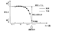
- FIG. 4 is a schematic diagram illustrating an example of predicting a change in brightness of an image based on a signal included in a region of interest;
- FIG. 4 is a diagram illustrating intensity distributions of a pair of subject images generated by a pair of light beams for focus detection;
- FIG. 8A is a diagram exemplifying an imaging range and a region of interest.
- FIG. 8B is a schematic diagram for explaining the photoelectric conversion time of a partial image shot in the region of interest and a
- FIG. 1 is a block diagram illustrating the configuration of an imaging device 1 equipped with an imaging element 3 according to an embodiment.
- the imaging apparatus 1 includes a photographic optical system 2 (21), an imaging device 3, a control section 4, a lens driving section 7, and an aperture driving section 8, and is configured such that a storage medium 5 such as a memory card is detachable.
- the imaging device 1 is, for example, a camera.
- the photographing optical system 2 has a plurality of lenses and a diaphragm 21 and forms a subject image on the image sensor 3 .
- the imaging device 3 captures a subject image formed by the imaging optical system 2 and generates an image signal.
- the imaging device 3 is, for example, a CMOS image sensor.
- the control unit 4 outputs a control signal for controlling the operation of the image sensor 3 to the image sensor 3 .
- the control unit 4 further functions as an image generating unit that performs various image processing on the image signal output from the imaging device 3 to generate image data.
- the control unit 4 also includes a focus detection unit 41 and an exposure control unit 42, which will be described later with reference to FIG. Based on a control signal from the control unit 4 (focus detection unit 41), the lens driving unit 7 moves the focusing lens constituting the photographic optical system 2 in the direction of the optical axis Ax in order to bring the main subject into focus.
- the diaphragm drive unit 8 adjusts the aperture diameter of the diaphragm 21 based on the control signal from the control unit 4 (exposure control unit 42), and adjusts the amount of light incident on the imaging device 3.
- FIG. The image data generated by the control unit 4 is recorded in the storage medium 5 in a predetermined file format.
- the imaging optical system 2 may be configured to be detachable from the imaging device 1 .
- FIG. 2 is a diagram illustrating the cross-sectional structure of the imaging device 3 of FIG.
- the imaging device 3 shown in FIG. 2 is a back-illuminated imaging device.
- the imaging device 3 includes a first substrate 111 , a second substrate 112 , a third substrate 113 and a fourth substrate 114 .
- the first substrate 111, the second substrate 112, the third substrate 113, and the fourth substrate 114 are each made of a semiconductor substrate or the like.
- the first substrate 111 is laminated on the second substrate 112 via the wiring layers 140 and 141 .
- the second substrate 112 is laminated on the third substrate 113 with the wiring layers 142 and 143 interposed therebetween.
- the third substrate 113 is stacked on the fourth substrate 114 with the wiring layers 144 and 145 interposed therebetween.
- the incident light L indicated by the white arrow enters in the positive direction of the Z axis. Also, as shown in the coordinate axes, the right direction on the paper surface perpendicular to the Z-axis is the positive X-axis direction, and the frontward direction on the paper surface perpendicular to the Z-axis and the X-axis is the positive Y-axis direction.
- the imaging device 3 has a first substrate 111, a second substrate 112, a third substrate 113, and a fourth substrate 114 stacked in the direction in which the incident light L is incident.
- the imaging device 3 further has a microlens layer 101 , a color filter layer 102 and a passivation layer 103 . These passivation layer 103 , color filter layer 102 and microlens layer 101 are sequentially laminated on the first substrate 111 .
- the microlens layer 101 has a plurality of microlenses ML.
- the microlens ML converges the incident light onto a photoelectric conversion section, which will be described later.
- the color filter layer 102 has a plurality of color filters F. As shown in FIG.
- the passivation layer 103 is composed of a nitride film or an oxide film.
- First substrate 111, second substrate 112, third substrate 113, and fourth substrate 114 have first surfaces 105a, 106a, 107a, and 108a on which gate electrodes and gate insulating films are provided, respectively. It has second surfaces 105b, 106b, 107b, and 108b. Various elements such as transistors are provided on the first surfaces 105a, 106a, 107a, and 108a, respectively.
- the first surface 105a of the first substrate 111, the first surface 106a of the second substrate 112, the first surface 107a of the third substrate 113, and the first surface 108a of the fourth substrate 114 are provided with wiring layers 140, 141, and 108a, respectively. 144 and 145 are laminated.
- Wiring layers (connection layers between substrates) 142 and 143 are laminated on the second surface 106b of the second substrate 112 and the second surface 107b of the third substrate 113, respectively.
- the wiring layers 140 to 145 are layers containing a conductor film (metal film) and an insulating film, and a plurality of wirings and vias are arranged in each layer.
- the elements on the first surface 105a of the first substrate 111 and the elements on the first surface 106a of the second substrate 112 are electrically connected via wiring layers 140 and 141 by connecting portions 109 such as bumps and electrodes.
- the elements on the first surface 107a of the third substrate 113 and the elements on the first surface 108a of the fourth substrate 114 are electrically connected through the wiring layers 144 and 145 by the connecting portions 109 such as bumps and electrodes.
- the second substrate 112 and the third substrate 113 have a plurality of through electrodes 110 .
- the through electrode 110 of the second substrate 112 connects the circuits provided on the first surface 106a and the second surface 106b of the second substrate 112 to each other, and the through electrode 110 of the third substrate 113
- the circuits provided on the first surface 107a and the second surface 107b are connected to each other.
- the circuit provided on the second surface 106b of the second substrate 112 and the circuit provided on the second surface 107b of the third substrate 113 are connected by connecting portions 109 such as bumps and electrodes via connecting layers 142 and 143 between substrates. electrically connected.
- the first substrate 111, the second substrate 112, the third substrate 113, and the fourth substrate 114 are laminated in the embodiment, the number of laminated substrates is larger than that in the embodiment. may be less.
- the first substrate 111, the second substrate 112, the third substrate 113, and the fourth substrate 114 may be called a first layer, a second layer, a third layer, and a fourth layer, respectively.
- FIG. 3 is a block diagram illustrating the configuration of each layer of the first substrate 111 to the fourth substrate 114 in the imaging device 3 according to the embodiment.
- the first substrate 111 has, for example, a plurality of pixels 10 arranged two-dimensionally and a signal readout section 20 .
- a plurality of arranged pixels 10 and readout units 20 may be referred to as a pixel array 210 .
- the pixels 10 are arranged side by side in the X-axis direction (row direction) and the Y-axis direction (column direction) shown in FIG.
- the pixel 10 has a photoelectric conversion unit such as a photodiode (PD) and converts incident light L into charges.
- PD photodiode
- the reading unit 20 is provided for each pixel 10 and reads out a signal (photoelectric conversion signal) based on charges photoelectrically converted by the corresponding pixel 10 .
- a readout control signal necessary for the readout unit 20 to read out signals from the pixels 10 is supplied from the in-sensor control unit 260 of the second substrate 112 to the readout unit 20 .
- a signal read by the readout unit 20 is sent to the second substrate 112 .
- the second substrate 112 has, for example, an A/D converter 230 and an in-sensor controller 260 .
- the A/D converter 230 converts the signal output from the corresponding pixel 10 into a digital signal.
- a signal converted by the A/D converter 230 is sent to the third substrate 113 .
- the in-sensor control unit 260 generates a readout control signal for the readout unit 20 based on the instruction signal input via the input unit 290 of the fourth substrate 114 .
- the instruction signal is sent from the image processing engine 30, which will be described later with reference to FIG.
- a readout control signal generated by the in-sensor controller 260 is sent to the first substrate 111 .
- the third substrate 113 has, for example, a memory 250 and a calculator 240 .
- Memory 250 stores the digital signal converted by A/D converter 230 .
- the calculator 240 performs a predetermined calculation using at least one of the digital signal stored in the memory 250 and the digital signal converted by the A/D converter 230 .
- the computation includes at least one of the computations exemplified below. (1) calculating information indicating the brightness of an image captured by the imaging device 3; (2) calculating information indicating the state of focus adjustment of the imaging optical system 2; What to do A live view image is an image for monitor display generated based on the digital signal converted by the A/D converter 230, and is also called a through image.
- the fourth substrate 114 has, for example, an output section 270 and an input section 290 .
- the output unit 270 outputs the digital signal stored in the memory 250, the digital signal converted by the A/D conversion unit 230, or information indicating the calculation result of the calculation unit 240 to the image processing engine 30 (see FIG. 5).
- An instruction signal from the image processing engine 30 is input to the input unit 290 .
- the instruction signal is sent to the second substrate 112 .
- FIG. 4 is a diagram for explaining an imaging range 50 imaged by the imaging element 3.
- a plurality of focus points P are provided in advance in the imaging range 50 .
- a focus point P indicates a position where the focus of the photographing optical system 2 can be adjusted in the photographing range 50, and is also called a focus detection area, a focus detection position, or a distance measuring point.
- FIG. 4 exemplifies a square mark indicating the focus point P superimposed on the live view image. It should be noted that the number of focus points P and their positions in the shooting range 50 shown in the figure are only examples, and are not limited to the mode of FIG.
- the control unit 4 detects an image shift between a pair of images caused by a pair of light beams passing through different regions of the imaging optical system 2 based on a photoelectric conversion signal from the pixel 10 having a photoelectric conversion unit for focus detection. Calculate the amount (phase difference).
- the image shift amount can be calculated for each focus point P.
- the amount of image shift between the pair of images is the basis for calculating the amount of defocus, which is the amount of shift between the position of the subject image formed by the light flux that has passed through the imaging optical system 2 and the position of the imaging surface of the imaging device 3.
- the defocus amount can be calculated by multiplying the image shift amount of the pair of images by a predetermined conversion coefficient.
- the control unit 4 further, for example, based on the image shift amount of the pair of images calculated at the focus point P corresponding to the subject closest to the imaging device 1 among the plurality of focus points P, A control signal for moving the focusing lens of the photographing optical system 2 is generated.
- the control unit 4 focus detection unit 41
- the user can select a focus point P by operating an operation member 6, which will be described later.
- FIG. 4 also illustrates frames indicating regions of interest T1 and T2.
- a region of interest T ⁇ b>1 surrounded by a dashed line is set by the control unit 4 .
- the control unit 4 exposure control unit 42 sets a region of interest T1 at a position including a main subject (for example, a person's face), and uses signals from the pixels 10 for image generation included in the region of interest T1. Brightness information (Bv value) is detected.
- the control unit 4 determines the aperture value (Av value), shutter speed (Tv value), and sensitivity (Sv value), for example, based on the information of the Bv value and the program chart.
- the control unit 4 captures the position of a person or the like detected by known image recognition processing performed based on live view image data, or the position input by the user operating an operation member 6 described later. It can be the location of the main subject in range 50 . It should be noted that the entire imaging range 50 may be set as the region of interest T1.
- a region of interest T2 surrounded by a solid line is also set by the control unit 4.
- the control unit 4 focus detection unit 41 sets, for example, a region of interest T2 in the row direction (the X-axis direction shown in FIG. 2) including the eyes of a person, and from the pixels 10 for focus detection included in the region of interest T2. can be used to calculate the image shift amount (phase difference) between the pair of images.
- the charge accumulation time can be controlled for each pixel 10 .
- each pixel 10 can output signals captured at different frame rates. Specifically, while one pixel 10 is caused to accumulate charge once, the other pixels 10 are caused to accumulate charges a plurality of times, thereby reading signals from the respective pixels 10 at different frame rates. It is configured so that it can be put out.
- the amplification gain for the signal output from the pixel 10 can be controlled for each pixel 10 .
- the amplification gain can be set so as to make the signal levels uniform. ing.
- FIG. 5 is a schematic diagram illustrating transfer of data and the like between the imaging device 3 and the image processing engine 30 according to the embodiment.
- the imaging device 3 picks up an image for recording, and sends data of the photographed image to the image processing engine 30 as image data for recording. do.
- the digital signal stored in the memory 250 can be sent as the data of the image for recording.
- the image sensor 3 captures a plurality of frames of images for monitor display, and converts the data of the captured images into live view image data. Send to processing engine 30 .
- the live-view image data is sent to the image processing engine 30, for example, the digital signal converted by the A/D converter 230 can be sent as the live-view image data.
- the imaging device 3 is configured to be able to send information indicating the calculation result of the calculation unit 240 to the image processing engine 30 in addition to image data.
- image processing engine 30 is included in control unit 4 .
- the image processing engine 30 has an image sensor control section 310 , an input section 320 , an image processing section 330 and a memory 340 .
- An operation member 6 including a release button, an operation switch, and the like is provided, for example, on the exterior surface of the imaging device 1 .
- the operation member 6 sends an operation signal according to the user's operation to the imaging element control section 310 .
- the user gives a photographing instruction to the imaging device 1 and a setting instruction of photographing conditions and the like.
- the imaging device control unit 310 sends information indicating the set imaging conditions to the imaging device 3 when an instruction to set imaging conditions and the like is given. Further, when a half-pressing operation signal indicating that the release button has been half-pressed with a stroke shorter than the full-pressing stroke is input from the operation member 6, the imaging device control unit 310 displays a display unit (not shown). Alternatively, in order to continuously display images for monitor display in the viewfinder, an instruction signal for instructing start of photographing for monitor display is sent to the image sensor 3 . Furthermore, when a full-press operation signal indicating that the release button has been fully-pressed with a stroke longer than that of the half-press operation is input from the operation member 6, the image sensor control unit 310 captures a still image for recording. An instruction signal for instructing start of photographing is sent to the imaging device 3 .
- the digital signal and the like output from the image sensor 3 are input to the input unit 320 .
- digital signals based on signals from the pixels 10 having photoelectric conversion units for image generation are sent to the image processing unit 330 .
- the image processing unit 330 performs predetermined image processing on the digital signal acquired from the image sensor 3 to generate image data.
- the generated image data for recording is recorded in the memory 340 or used for displaying a confirmation image after photographing.
- the image data recorded in the memory 340 can be recorded in the storage medium 5 described above.
- the generated image data for monitor display is used for display on a viewfinder or the like.
- live view image signals based on signals from the pixels 10 having photoelectric conversion units for image generation are also sent to the exposure control unit 42 and used for exposure calculation.
- the exposure calculation determines the aperture value, shutter speed, and sensitivity described above.
- digital signals based on signals from the pixels 10 having photoelectric conversion units for focus detection are sent to the focus detection unit 41 and used for focus detection calculation.
- the defocus amount described above is calculated by the focus detection calculation.
- Information indicating the focus adjustment state of the imaging optical system 2 input to the input unit 320 is used by the control unit 4 to determine the validity of the focus adjustment.
- ⁇ Image sensor> In addition to the pixel array 210, the A/D conversion unit 230, the calculation unit 240, the memory 250, the in-sensor control unit 260, the input unit 290 and the output unit 270 described with reference to FIG. 220.
- the amplifier 220 can be provided on the first substrate 111 of FIG.
- the amplification section 220 amplifies the signal output from the pixel 10 and sends the amplified signal to the A/D conversion section 220 .
- the in-sensor control unit 260 performs the following setting processing.
- the in-sensor control unit 260 sets the amplification gain for the amplification unit 220 based on information indicating the brightness of the image, which will be described later.
- the amplification gain can be set for each pixel 10.
- the amplification gain for the signals of all the pixels 10 included in the imaging range 50 can be made the same, or the amplification gain can be set for the signals of the pixels 10 included in the region of interest T1 or T2.
- the gain can be different from the amplification gain for signals of other pixels 10 .
- the in-sensor control unit 260 sets the photoelectric conversion time (in other words, accumulation time) for the pixels 10 in the imaging range 50 based on information indicating the brightness of the image, which will be described later.
- the photoelectric conversion time can be set for each pixel 10.
- the photoelectric conversion time of all the pixels 10 included in the imaging range 50 can be set to be the same, or the photoelectric conversion time of the pixels 10 included in the region of interest T1 or T2 can be set to the same value. can be made different from the photoelectric conversion time of other pixels 10 .
- the calculator 240 can perform the following processes. 1. Calculation of Information Indicating Brightness of Image
- the calculation unit 240 of the imaging device 3 outputs from the pixels 10 having a photoelectric conversion unit for image generation included in the region of interest T1, for example, and converts the information by the A/D conversion unit 230. Information indicating the brightness of the image is calculated based on the obtained digital signal.
- the information calculated by the calculation unit 240 is sent to the in-sensor control unit 260 and used for the setting process described above.
- Information indicating the region of interest T ⁇ b>1 set by the control unit 4 is transmitted to the imaging device 3 via the image processing engine 30 .
- FIG. 6 is a schematic diagram illustrating an example in which the calculation unit 240 predicts changes in brightness of an image based on signals from pixels 10 having photoelectric conversion units for image generation included in the region of interest T1.
- the horizontal axis indicates the number of frames of the live view image, and the vertical axis indicates the brightness of the image.
- the partial image in the region of interest T1 is read out at high speed equivalent to 150 fps, which is five times the live view image.
- An image in the region of interest T1 is called a partial image.
- the white circles in FIG. 6 indicate the readout timing of the live view image. It is assumed that the live view image includes the most recently read N frames and the previous N ⁇ 1 frames. Also, the black circles in FIG. 6 indicate the readout timing of the partial image in the region of interest T1. Five frames of partial images are read out while one frame of the live view image is read out.
- the calculation unit 240 calculates the average value of the digital signals forming the partial image, and uses the calculated average value as the brightness information of the partial image.
- the average value of the digital signals forming the partial image can be calculated five times while the live view image of one frame is being read.
- the brightness of the partial image gradually decreases during the shooting of the live view image of the N+1th frame.
- the calculation unit 240 extrapolates the brightness at the read timing of the live view image of the N+1th frame based on the amount of temporal change in the brightness of the partial image.
- the predicted value calculated by the calculator 240 is used by the in-sensor controller 260 as follows.
- the in-sensor control unit 260 calculates the amount of change in brightness at the readout timing of the N+1th frame live view image predicted by the calculation unit 240 (the brightness at the readout timing of the Nth frame and the predicted value at the readout timing of the N+1th frame ), the amplification gain for the signals of all the pixels 10 included in the imaging range 50 is increased, or the signal of all the pixels 10 included in the imaging range 50 is increased or Setting processing based on the information indicating the brightness of the image is performed by, for example, lengthening the photoelectric conversion time of 10 .
- the in-sensor control unit 260 detects the change in brightness at the readout timing of the N+1th frame live view image predicted by the calculation unit 240.
- the amplification gain for the signals of all the pixels 10 included in the shooting range 50 is lowered, or the photoelectric conversion of all the pixels 10 included in the shooting range 50 is reduced.
- Setting processing is performed based on the information indicating the brightness of the image, such as by shortening the conversion time.
- At least one of the amplification gain and the photoelectric conversion time at the time of photographing is set.
- the in-sensor control unit 260 performs at least one of setting the gain for the amplification unit 220 and setting the photoelectric conversion time for the pixels 10 based on the information indicating the brightness of the image calculated by the calculation unit 240 . Since it is configured in this way, feedback control can be performed within the imaging element 3 to bring the brightness of the image closer to an appropriate level, for example. Therefore, the amount of data and the like to be transmitted between the imaging element 3 and the external circuit or the like can be reduced.
- the calculation unit 240 of the image sensor 3 outputs, for example, from the pixel 10 having a photoelectric conversion unit for focus detection included in the region of interest T2, and outputs the A/D conversion unit Information indicating the intensity distribution of the signals from the focus detection pixels is calculated based on the digital signals converted in 230 .
- the information calculated by the calculation unit 240 is transmitted to the control unit 4 via the output unit 270 and used to determine the validity of focus adjustment.
- Information indicating the region of interest T ⁇ b>2 set by the control unit 4 is transmitted to the image sensor 3 via the image processing engine 30 .
- FIG. 7 is a diagram illustrating the intensity distribution of a pair of subject images generated by the above-described pair of light beams for focus detection.
- the horizontal axis indicates the position in the X-axis direction of the pixels 10 in which the photoelectric conversion units for focus detection are arranged, and the vertical axis indicates the signal value of the digital signal.
- the above-mentioned pair of light beams are A and B
- the image generated by the light beam A is represented by the curve 71
- the image generated by the light beam B is represented by the curve 72.
- the curve 72 is a curve based on the signal values read from the pixels 10 receiving the luminous flux B.
- the partial image in the region of interest T2 is read at high speed equivalent to 150 fps, which is five times the live view image.
- the calculation unit 240 calculates the difference between the average value of the digital signal values indicating the intensity distribution of the subject image indicated by the curve 71 and the average value of the digital signal values indicating the intensity distribution of the subject image indicated by the curve 72. Calculate That is, while one frame of the live view image for monitor display is being read out, the difference between the average values based on the signals of the partial images can be calculated five times.
- the difference between the average values calculated by the calculation unit 240 is sent to the image processing engine 30 (that is, the control unit 4) as information indicating the focus adjustment state of the imaging optical system 2.
- the difference between the average values calculated by the calculator 240 is used by the controller 4 as follows.
- the control unit 4 determines the validity of the focus adjustment based on the information calculated by the calculation unit 240 of the imaging device 3.
- the example of FIG. 7 is an example in which the signal value indicated by the curve 72 is lower than the signal value indicated by the curve 71 by an allowance or more due to the difference in the amount of light between the light beams A and B for focus detection. In this way, when the curve 71 and the curve 72 based on a pair of light beams A and B with a low degree of coincidence, in which there is a difference greater than the allowable difference between the curves 71 and 72, a pair of It becomes difficult to accurately calculate the image shift amount of the image of the subject.
- the control unit 4 determines whether the focus adjustment is appropriate. It is determined that the lens is missing, and the focus detection unit 41 is not caused to generate a control signal for moving the focusing lens of the photographing optical system 2 .
- the adequacy of focus adjustment can be judged in a short period of time while one frame of live view image is being photographed, and useless driving of the focusing lens can be avoided when the adequacy is lacking.
- the control unit 4 determines the validity of focus adjustment based on the intensity distribution of the images of the two subjects based on the light beams A and B.
- the validity of the focus adjustment may be determined based on whether or not the peak value of the intensity distribution of the image exceeds a predetermined determination threshold.
- the calculator 240 in this case calculates the peak value of the intensity distribution of the subject image indicated by the curve 71 or curve 72 .
- the peak value of the intensity distribution of the object image calculated by the calculation unit 240 is sent to the image processing engine 30 (that is, the control unit 4) as information indicating the focus adjustment state of the imaging optical system 2.
- control unit 4 determines that the focus adjustment lacks validity, and causes the focus detection unit 41 to move the focusing lens of the photographic optical system 2. Do not generate control signals for
- the control unit 4 determines that the peak coordinates of the intensity distribution of the image of the subject in row A or row B (in other words, the position in the X-axis direction of the pixels 10 in which the photoelectric conversion units for focus detection are arranged)
- the validity of the focus adjustment may be determined based on whether or not it is within a predetermined range from the center of the range 50 .
- the calculator 240 in this case calculates the peak coordinates of the intensity distribution of the subject image indicated by the curve 71 or curve 72 .
- the peak coordinates calculated by the calculation unit 240 are sent to the image processing engine 30 (that is, the control unit 4) via the output unit 270 as information indicating the state of focus adjustment of the imaging optical system 2.
- FIG. When the peak coordinate of the intensity distribution of the image of the subject is not included in the predetermined range from the center of the photographing range 50, the control unit 4 determines that the focus adjustment lacks validity. do not generate a control signal to move the focusing lens.
- control unit 4 determines the validity of the focus adjustment based on whether or not the variation width of the intensity distribution of the image of the subject in row A or row B is less than a predetermined value (in other words, the contrast of the image is insufficient). It may be configured to determine The calculation unit 240 in this case calculates the variation width based on the intensity distribution of the subject image indicated by the curve 71 or curve 72 . The variation width calculated by the calculation unit 240 is sent to the image processing engine 30 (that is, the control unit 4) via the output unit 270 as information indicating the focus adjustment state of the imaging optical system 2. FIG. The control unit 4 determines that the focus adjustment is not appropriate when the variation width of the intensity distribution of the image of the object is less than a predetermined value, and instructs the focus detection unit 41 to move the focusing lens of the photographing optical system 2. Do not generate control signals.
- the photoelectric conversion time of the partial image is the photoelectric conversion time of the live view image. (eg 1/5) compared to . Therefore, when the amplification gain for the signal is set to the same extent for the live-view image and the partial image, the signal level of the partial image per frame is smaller than the signal level of the live-view image (for example, 1 /5).
- the calculation unit 240 of the embodiment performs complementary processing so that the signal level of the partial image of the region of interest T1 approaches the signal level of the live view image. For example, with respect to the digital signal from the region of interest T1, digital signals of partial images of 5 frames read out at a higher frame rate (for example, 5 times) than the live view image are added for each pixel 10, and the gain is adjusted as necessary. After adjustment, it is embedded in the region of interest T1 in the live-view image and complemented as one live-view image.
- FIG. 8(a) is a diagram illustrating an imaging range 50 and a region of interest T1 imaged by the imaging device 3.
- FIG. 8B is a schematic diagram illustrating photoelectric conversion times for a partial image shot in the region of interest T1 and a live view image shot outside the region of interest T1.
- FIG. 8B illustrates a case where five frames of partial images are read from the region of interest T1 while one frame of the live view image is read.
- the memory 250 stores a digital signal based on the pixels 10 corresponding to the entire shooting range 50 captured by the image sensor 3 and a part of the shooting range 50 (region of interest T1 or T2) based on the pixel 10 can be stored.
- the memory 250 has a storage capacity capable of storing at least a plurality of frames (for example, 20 frames) of partial images and at least one frame of the entire image. Since the number of signals forming the partial image is smaller than the number of signals forming the entire image of the photographing range 50, the storage capacity of the memory 250 can be reduced compared to the case of storing a plurality of frames of the entire image.
- the calculation unit 240 adds partial images of a plurality of frames captured in the region of interest T1 at a frame rate higher than that of the live view image, and uses the signals of the partial images after the addition to obtain images of regions other than the region of interest T1. Complement the live view image taken in the area. Since it is configured in this way, it is possible to perform complementing processing of the live view image within the imaging device 3 .
- the image sensor 3 detects the brightness of an image based on signals output from a plurality of pixels 10 that output signals based on photoelectrically converted charges and a region of interest T1 that is a part of the plurality of pixels 10. and at least one of the information used to determine the appropriateness of focus adjustment as an evaluation value; and an in-sensor controller 260 that controls at least one of the photoelectric conversion time and the amplification gain for the signal in the pixels 10 of the region of interest T1.
- the image pickup device 3 compared to the case where the signal photoelectrically converted by the image pickup device 3 is output to the outside of the image pickup device 3 and the evaluation value is calculated by an external image processing engine 30 or the like, the image pickup device 3 The number of data output to the image processing engine 30 can be reduced. As a result, the processing time for the image sensor 3 to output data and the power consumption in the image sensor 3 can be reduced. In addition, feedback control of at least one of photoelectric conversion time and amplification gain for the pixels 10 of the image pickup device 3 can be performed inside the image pickup device 3 .
- the signal photoelectrically converted by the image sensor 3 is output to the outside of the image sensor 3, an evaluation value is calculated by an external image processing engine 30 or the like, and feedback control of the photoelectric conversion time or amplification gain is performed based on this evaluation value. is performed from the outside of the imaging device 3, at least the time required for transmitting and receiving data can be omitted, so feedback control can be performed in a short time.
- the calculation unit 240 of the imaging device 3 extrapolates the evaluation value based on the temporal change in the calculated evaluation value. With this configuration, it becomes possible to appropriately control the photoelectric conversion time or the amplification gain of the pixels 10 when capturing a live view image of the next frame, for example.
- the signals output from the pixels 10 of the image sensor 3 are a first signal as a live view image output from all of the plurality of pixels 10 for monitor display, and a plurality of pixels 10 for calculating evaluation values.
- the calculation unit 240 calculates an evaluation value based on the second signal. With this configuration, the calculation unit 240 can appropriately calculate the evaluation value using the second signal that is output separately from the first signal that is output for monitor display.
- the frame rate at which the second signal is output from the pixels 10 of the imaging element 3 is higher than the frame rate at which the first signal is output.
- the calculation unit 240 can calculate the evaluation value based on the second signal five times while the live view image (first signal) for monitor display of one frame is read. Therefore, it is possible to appropriately control the photoelectric conversion time or amplification gain for the live view image of the next frame based on the five calculated evaluation values.
- the calculation unit 240 of the image pickup device 3 adds, for example, five frames of the second signals forming the partial images output from the pixels 10 of the region of interest T1, and uses the added signals to calculate the pixels 10 of the region of interest T1. Complement the first signal corresponding to the position. Since it is configured in this way, the live view image complementing process can be appropriately performed within the imaging device 3 .
- the imaging device 1 determines the validity of the focus adjustment of the photographic optical system 2 based on the image sensor 3 and the information output from the image sensor 3 and used as an evaluation value for determining the validity of the focus adjustment.
- a control unit 4 is provided.
- the calculation unit 240 can calculate the information used to determine the validity of focus adjustment five times while one frame of the live view image for monitor display is being read. Therefore, compared to the case where the focus detection unit 41 of the control unit 4 performs the focus detection calculation using the signals of the focus detection pixels transmitted from the image sensor 3 at the same timing as the signals of the live view image, the speed is five times faster. It is possible to judge the adequacy of focus adjustment at a low level.
- the imaging element 3 is configured as a backside illumination type.
- the imaging element 3 may have a surface-illuminated configuration in which the wiring layer 140 is provided on the light incident surface side.
- Modification 2 In the embodiment described above, an example using a photodiode as a photoelectric conversion unit has been described. However, a photoelectric conversion film may be used as the photoelectric conversion portion.
- the imaging device 3 may be applied to a camera, a smartphone, a tablet, a camera built into a PC, an in-vehicle camera, and the like.
- the in-sensor control unit 260 controls at least one of the gain setting for the amplification unit 220 and the photoelectric conversion time setting for the pixels 10 based on the information indicating the brightness of the image calculated by the calculation unit 240.
- the information indicating the brightness of the image calculated by the calculation unit 240 is sent to the control unit 4, and the exposure control unit 42 of the control unit 4 performs exposure calculation based on the information indicating the brightness of the image, and controls the exposure.
- the section 4 may be configured to control the aperture driving section 8 based on the exposure calculation result.
- the information indicating the brightness of the image calculated by the calculator 240 is sent to the image processing engine 30 (that is, the controller 4) via the output unit 270.
- the exposure control unit 42 of the control unit 4 performs exposure calculations based on the information sent from the image sensor 3, and controls the aperture value, shutter speed, and sensitivity described above.
- the exposure control section 42 and the aperture driving section 8 may be collectively referred to as a light amount adjusting section 9 (FIG. 5) for adjusting the amount of light incident on the image pickup device 3 .
- the calculation unit 240 can calculate the information indicating the brightness of the image five times while one frame of the live view image for monitor display is being read. Therefore, when the exposure control unit 42 of the control unit 4 performs the exposure calculation using the information indicating the brightness of the image calculated by the calculation unit 240, the signal of the live view image sent from the image pickup device 3 is used for exposure. Exposure calculation can be performed at a speed five times faster than when calculation is performed, and followability to changes in image brightness can be enhanced. In Modified Example 4, the number of times the information indicating the brightness of the image calculated by the calculation unit 240 is sent to the image processing engine 30 (that is, the control unit 4) increases. Since the number of signals of the information indicating the brightness of is sufficiently small compared to the signals forming the live view image, the amount of data sent from the imaging device 3 to the control unit 4 does not increase significantly.
- the information indicating the intensity distribution of the pair of subject images generated by the pair of light beams for focus detection calculated by the calculator 240 is sent to the image processing engine 30 (that is, the control 4).
- a focus detection unit 41 of the control unit 4 performs focus detection calculation based on information sent from the image sensor 3 and sends a control signal for moving the focusing lens to the lens driving unit 7 .
- the calculation unit 240 can calculate the intensity distribution of the pair of subject images five times while one frame of the live view image for monitor display is read. Therefore, when the focus detection unit 41 of the control unit 4 performs focus detection calculation using the information indicating the intensity distribution of the images of the pair of subjects calculated by the calculation unit 240, the signal from the image sensor 3 is the same as the signal of the live view image. Computation can be performed at a speed five times faster than when focus detection computation is performed using the signals of the focus detection pixels transmitted at the timing, and tracking to changes in subject distance can be enhanced.
- the present invention is not limited to the contents of the embodiments and modifications.
- the scope of the present invention also includes a mode in which each configuration shown in the embodiment and modifications is used in combination.
- Other aspects conceivable within the scope of the technical idea of the present invention are also included in the scope of the present invention.
Landscapes
- Engineering & Computer Science (AREA)
- Signal Processing (AREA)
- Multimedia (AREA)
- Computer Networks & Wireless Communication (AREA)
- Studio Devices (AREA)
- Transforming Light Signals Into Electric Signals (AREA)
Priority Applications (3)
| Application Number | Priority Date | Filing Date | Title |
|---|---|---|---|
| US18/563,593 US20240276105A1 (en) | 2021-05-24 | 2022-05-23 | Imaging element and imaging device |
| JP2023523455A JPWO2022250000A1 (https=) | 2021-05-24 | 2022-05-23 | |
| CN202280036743.7A CN117397253A (zh) | 2021-05-24 | 2022-05-23 | 摄像元件以及摄像装置 |
Applications Claiming Priority (2)
| Application Number | Priority Date | Filing Date | Title |
|---|---|---|---|
| JP2021-087030 | 2021-05-24 | ||
| JP2021087030 | 2021-05-24 |
Publications (1)
| Publication Number | Publication Date |
|---|---|
| WO2022250000A1 true WO2022250000A1 (ja) | 2022-12-01 |
Family
ID=84229875
Family Applications (1)
| Application Number | Title | Priority Date | Filing Date |
|---|---|---|---|
| PCT/JP2022/021043 Ceased WO2022250000A1 (ja) | 2021-05-24 | 2022-05-23 | 撮像素子および撮像装置 |
Country Status (4)
| Country | Link |
|---|---|
| US (1) | US20240276105A1 (https=) |
| JP (1) | JPWO2022250000A1 (https=) |
| CN (1) | CN117397253A (https=) |
| WO (1) | WO2022250000A1 (https=) |
Citations (3)
| Publication number | Priority date | Publication date | Assignee | Title |
|---|---|---|---|---|
| JP2014143667A (ja) * | 2012-12-28 | 2014-08-07 | Canon Inc | 撮像素子、撮像装置、その制御方法、および制御プログラム |
| JP2015521390A (ja) * | 2012-06-04 | 2015-07-27 | ソニー株式会社 | 半導体装置及び検出システム |
| JP2018129789A (ja) * | 2017-02-10 | 2018-08-16 | キヤノン株式会社 | 撮像素子および撮像装置 |
Family Cites Families (5)
| Publication number | Priority date | Publication date | Assignee | Title |
|---|---|---|---|---|
| BR112014027066A2 (pt) * | 2012-05-02 | 2017-06-27 | Nikon Corp | dispositivo de formação de imagem |
| JP2016171455A (ja) * | 2015-03-12 | 2016-09-23 | 株式会社東芝 | 固体撮像装置 |
| JP2017184094A (ja) * | 2016-03-31 | 2017-10-05 | ソニー株式会社 | 撮像制御装置、撮像制御方法、コンピュータプログラム及び電子機器 |
| CN116995085A (zh) * | 2016-03-31 | 2023-11-03 | 株式会社尼康 | 摄像元件 |
| JP6638852B1 (ja) * | 2018-08-31 | 2020-01-29 | ソニー株式会社 | 撮像装置、撮像システム、撮像方法および撮像プログラム |
-
2022
- 2022-05-23 WO PCT/JP2022/021043 patent/WO2022250000A1/ja not_active Ceased
- 2022-05-23 US US18/563,593 patent/US20240276105A1/en active Pending
- 2022-05-23 CN CN202280036743.7A patent/CN117397253A/zh active Pending
- 2022-05-23 JP JP2023523455A patent/JPWO2022250000A1/ja active Pending
Patent Citations (3)
| Publication number | Priority date | Publication date | Assignee | Title |
|---|---|---|---|---|
| JP2015521390A (ja) * | 2012-06-04 | 2015-07-27 | ソニー株式会社 | 半導体装置及び検出システム |
| JP2014143667A (ja) * | 2012-12-28 | 2014-08-07 | Canon Inc | 撮像素子、撮像装置、その制御方法、および制御プログラム |
| JP2018129789A (ja) * | 2017-02-10 | 2018-08-16 | キヤノン株式会社 | 撮像素子および撮像装置 |
Also Published As
| Publication number | Publication date |
|---|---|
| US20240276105A1 (en) | 2024-08-15 |
| CN117397253A (zh) | 2024-01-12 |
| JPWO2022250000A1 (https=) | 2022-12-01 |
Similar Documents
| Publication | Publication Date | Title |
|---|---|---|
| US8063978B2 (en) | Image pickup device, focus detection device, image pickup apparatus, method for manufacturing image pickup device, method for manufacturing focus detection device, and method for manufacturing image pickup apparatus | |
| JP5396566B2 (ja) | 撮像装置及びそのオートフォーカス制御方法 | |
| JP7473041B2 (ja) | 撮像素子、及び撮像装置 | |
| JP6413233B2 (ja) | 撮像装置および撮像素子 | |
| JP2014178603A (ja) | 撮像装置 | |
| CN102227665A (zh) | 固态摄像元件和摄像设备 | |
| JP2015195235A (ja) | 固体撮像素子、電子機器、および撮像方法 | |
| JPWO2017169479A1 (ja) | 撮像素子、及び、撮像装置 | |
| JP2012191400A (ja) | 撮像素子および撮像装置 | |
| CN101779154A (zh) | 摄像装置和照相机 | |
| JP2014179892A (ja) | 撮像装置 | |
| CN104641276A (zh) | 摄像装置及信号处理方法 | |
| JP2016224278A (ja) | 撮像装置及び撮像素子の制御方法 | |
| CN110495165B (zh) | 摄像元件及摄像装置 | |
| WO2015080163A1 (ja) | 電子機器、撮像装置、および、撮像素子 | |
| JP6808420B2 (ja) | 撮像素子および撮像装置 | |
| JP2023133378A (ja) | 撮像装置 | |
| JP6488545B2 (ja) | 電子機器 | |
| JP5486284B2 (ja) | 撮像装置 | |
| WO2022250000A1 (ja) | 撮像素子および撮像装置 | |
| JP2018163322A (ja) | 撮像装置及びその制御方法、プログラム、記憶媒体 | |
| JP2012165070A (ja) | 固体撮像素子及びこれを用いた撮像装置 | |
| JP2019213216A (ja) | 制御装置、移動体および通信方法 | |
| JP2018033192A (ja) | 撮像装置 | |
| JP7632599B2 (ja) | 撮像素子および撮像装置 |
Legal Events
| Date | Code | Title | Description |
|---|---|---|---|
| 121 | Ep: the epo has been informed by wipo that ep was designated in this application |
Ref document number: 22811270 Country of ref document: EP Kind code of ref document: A1 |
|
| WWE | Wipo information: entry into national phase |
Ref document number: 202280036743.7 Country of ref document: CN |
|
| WWE | Wipo information: entry into national phase |
Ref document number: 18563593 Country of ref document: US |
|
| WWE | Wipo information: entry into national phase |
Ref document number: 2023523455 Country of ref document: JP |
|
| NENP | Non-entry into the national phase |
Ref country code: DE |
|
| 122 | Ep: pct application non-entry in european phase |
Ref document number: 22811270 Country of ref document: EP Kind code of ref document: A1 |