WO2022249689A1 - 端子金具 - Google Patents
端子金具 Download PDFInfo
- Publication number
- WO2022249689A1 WO2022249689A1 PCT/JP2022/013445 JP2022013445W WO2022249689A1 WO 2022249689 A1 WO2022249689 A1 WO 2022249689A1 JP 2022013445 W JP2022013445 W JP 2022013445W WO 2022249689 A1 WO2022249689 A1 WO 2022249689A1
- Authority
- WO
- WIPO (PCT)
- Prior art keywords
- wiring board
- plate
- flexible printed
- printed wiring
- terminal fitting
- Prior art date
- Legal status (The legal status is an assumption and is not a legal conclusion. Google has not performed a legal analysis and makes no representation as to the accuracy of the status listed.)
- Ceased
Links
Images



Classifications
-
- H—ELECTRICITY
- H01—ELECTRIC ELEMENTS
- H01R—ELECTRICALLY-CONDUCTIVE CONNECTIONS; STRUCTURAL ASSOCIATIONS OF A PLURALITY OF MUTUALLY-INSULATED ELECTRICAL CONNECTING ELEMENTS; COUPLING DEVICES; CURRENT COLLECTORS
- H01R12/00—Structural associations of a plurality of mutually-insulated electrical connecting elements, specially adapted for printed circuits, e.g. printed circuit boards [PCB], flat or ribbon cables, or like generally planar structures, e.g. terminal strips, terminal blocks; Coupling devices specially adapted for printed circuits, flat or ribbon cables, or like generally planar structures; Terminals specially adapted for contact with, or insertion into, printed circuits, flat or ribbon cables, or like generally planar structures
- H01R12/50—Fixed connections
- H01R12/59—Fixed connections for flexible printed circuits, flat or ribbon cables or like structures
- H01R12/592—Fixed connections for flexible printed circuits, flat or ribbon cables or like structures connections to contact elements
-
- H—ELECTRICITY
- H01—ELECTRIC ELEMENTS
- H01R—ELECTRICALLY-CONDUCTIVE CONNECTIONS; STRUCTURAL ASSOCIATIONS OF A PLURALITY OF MUTUALLY-INSULATED ELECTRICAL CONNECTING ELEMENTS; COUPLING DEVICES; CURRENT COLLECTORS
- H01R12/00—Structural associations of a plurality of mutually-insulated electrical connecting elements, specially adapted for printed circuits, e.g. printed circuit boards [PCB], flat or ribbon cables, or like generally planar structures, e.g. terminal strips, terminal blocks; Coupling devices specially adapted for printed circuits, flat or ribbon cables, or like generally planar structures; Terminals specially adapted for contact with, or insertion into, printed circuits, flat or ribbon cables, or like generally planar structures
- H01R12/50—Fixed connections
- H01R12/59—Fixed connections for flexible printed circuits, flat or ribbon cables or like structures
- H01R12/61—Fixed connections for flexible printed circuits, flat or ribbon cables or like structures connecting to flexible printed circuits, flat or ribbon cables or like structures
-
- H—ELECTRICITY
- H01—ELECTRIC ELEMENTS
- H01R—ELECTRICALLY-CONDUCTIVE CONNECTIONS; STRUCTURAL ASSOCIATIONS OF A PLURALITY OF MUTUALLY-INSULATED ELECTRICAL CONNECTING ELEMENTS; COUPLING DEVICES; CURRENT COLLECTORS
- H01R12/00—Structural associations of a plurality of mutually-insulated electrical connecting elements, specially adapted for printed circuits, e.g. printed circuit boards [PCB], flat or ribbon cables, or like generally planar structures, e.g. terminal strips, terminal blocks; Coupling devices specially adapted for printed circuits, flat or ribbon cables, or like generally planar structures; Terminals specially adapted for contact with, or insertion into, printed circuits, flat or ribbon cables, or like generally planar structures
- H01R12/50—Fixed connections
- H01R12/59—Fixed connections for flexible printed circuits, flat or ribbon cables or like structures
- H01R12/65—Fixed connections for flexible printed circuits, flat or ribbon cables or like structures characterised by the terminal
- H01R12/69—Fixed connections for flexible printed circuits, flat or ribbon cables or like structures characterised by the terminal deformable terminals, e.g. crimping terminals
-
- H—ELECTRICITY
- H01—ELECTRIC ELEMENTS
- H01R—ELECTRICALLY-CONDUCTIVE CONNECTIONS; STRUCTURAL ASSOCIATIONS OF A PLURALITY OF MUTUALLY-INSULATED ELECTRICAL CONNECTING ELEMENTS; COUPLING DEVICES; CURRENT COLLECTORS
- H01R13/00—Details of coupling devices of the kinds covered by groups H01R12/70 or H01R24/00 - H01R33/00
- H01R13/02—Contact members
- H01R13/10—Sockets for co-operation with pins or blades
- H01R13/11—Resilient sockets
- H01R13/114—Resilient sockets co-operating with pins or blades having a square transverse section
Definitions
- the present disclosure relates to terminal fittings.
- the terminal fitting disclosed in Patent Document 1 is configured to be connected to the wiring of a printed wiring circuit in which wiring is formed on a printed wiring board by ultrasonic welding or the like.
- the terminal fitting of the present disclosure has been perfected based on the circumstances described above, and can suppress the tensile force from reaching the connection portion with the flexible printed circuit board.
- the terminal fitting of the present disclosure is a connecting portion connected to the front end portion of the flexible printed wiring board; a fixing portion positioned rearward of the connection portion at the rear end portion and fixed to the flexible printed wiring board; Prepare.
- FIG. 1 is a front perspective view of a terminal fitting connected to a wiring board.
- FIG. 2 is a rear perspective view of the terminal fitting connected to the wiring board.
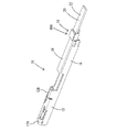
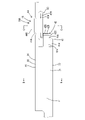
- FIG. 3 is a side view of part of the terminal fitting in FIG. 1 as seen from the right side. 4 is a plan view showing a part of the terminal fitting of FIG. 1.
- FIG. 5 is a bottom view showing part of the terminal fitting of FIG. 1.
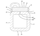
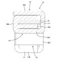
- FIG. 6 is a cross-sectional view taken along line AA of FIG.
- the terminal fitting of the present disclosure is (1) a connecting portion connected to the front end portion of the flexible printed wiring board; a fixing portion positioned rearward of the connection portion at the rear end portion and fixed to the flexible printed wiring board; Prepare.
- the tensile force acts on the entire terminal fitting via the fixing portion. Therefore, the tensile force can be suppressed from reaching the connecting portion between the connecting portion and the flexible printed wiring board. Therefore, it is possible to prevent the flexible printed wiring board from being detached from the connecting portion.
- the flexible printed wiring board is configured by extending a conductive path on one surface of a resin base material, and the fixing portion includes a long part in contact with the conductive path and a short part in contact with the other surface of the base material. , and the short portion preferably bites into the other surface of the substrate. According to this configuration, the short portion bites into the other surface of the resin base material, thereby improving the fixing force of the fixing portion to the flexible printed wiring board. Since the long portion cuts into the flexible printed wiring board more shallowly than the short portion, deformation of the conductive path is suppressed.
- the connecting portion has a pair of side plate portions, an upper plate portion connected to the upper edges of the side plate portions, and a single lower plate portion connecting the lower edges of the side plate portions.
- the upper plate portion protrudes from the pair of side plate portions through the arc-shaped portion, and is constituted by a pair of connection plate portions in which the projecting ends are butted against each other. It is preferable that the plates are connected and the pair of arcuate portions protrude outward from the left and right side edges of the flexible printed wiring board.
- the solder fillets are formed on both the left and right sides of the flexible printed wiring board at the connection portion between the flexible printed wiring board and the connecting portion. It becomes easy to contact the edge and the arcuate portion. Therefore, high connection strength can be obtained between the flexible printed wiring board and the connecting portion.
- the fixed portion extends from the single plate-like lower plate portion, the width dimension is easily ensured.
- the fixing portion has a rising portion that rises from the lower plate portion toward the flexible printed wiring board and a support portion that supports the rising portion from behind. According to this configuration, when a tensile force acts on the flexible printed wiring board, the rising portion tends to tilt backward, but the tilting of the rising portion is suppressed by the supporting portion.
- the fixing portion is made of a metal plate material and has a substrate portion in contact with one surface of the flexible printed wiring board and a crimped portion extending from the substrate portion and surrounding the flexible printed wiring board.
- a layered structure is preferred. According to this configuration, even if the metal plate material is thin in the fixing portion, the double-plate structure of the substrate portion can increase the rigidity and improve the fixing strength.
- FIG. 1 A first embodiment embodying the terminal fitting of the present disclosure will be described with reference to FIGS. 1 to 8.
- FIG. 1 the vertical directions shown in FIGS. 1 to 3 and 6 to 8 are defined as upward and downward.
- left and right appearing in FIGS. 2 to 6 are defined as forward and rearward, respectively.
- left and right directions the front and rear appearing in FIG. 1 are defined as left and right, respectively.
- a terminal metal fitting 10 of the first embodiment shown in FIGS. 1 and 2 is connected to a flexible printed wiring board (hereinafter also simply referred to as a wiring board) 20 .
- the wiring board 20 is configured by extending a conductive path (not shown) on one surface (lower surface) of a base material 22 made of resin.
- the base material 22 is composed of, for example, an insulating resin sheet.
- the conductive paths are made of copper foil, for example.
- the wiring board 20 is assembled in a connector housing (not shown), for example, to constitute a connector (not shown).
- the wiring board 20 is configured in a strip shape (strip shape).
- a terminal fitting 10 is connected to the front end side of the wiring board 20 .
- the terminal fitting 10 is, for example, a female terminal fitting, as shown in FIGS.
- the terminal fitting 10 is a single piece made of metal material.
- the terminal fitting 10 is formed by pressing or bending a conductive metal plate.
- the terminal fitting 10 has an elongated cylindrical shape as a whole.
- the terminal fitting 10 includes a body portion 12 , a connection portion 14 and a fixing portion 16 .
- the main body 12 has a square tubular shape penetrating in the front-rear direction.
- a male tab (not shown) of a male terminal fitting is inserted into the body portion 12 .
- the body portion 12 is provided with, for example, a first protrusion 12A, a second protrusion 12B, and the like.
- the first protrusion 12A and the second protrusion 12B are formed, for example, in a convex shape that is pressed outward and protrudes upward.
- the first projection 12A and the second projection 12B regulate the insertion of the terminal fitting 10 into the connector housing (not shown). abbreviated).
- the connecting portion 14 has a square tubular shape penetrating in the front-rear direction.
- the connecting portion 14 is positioned behind the body portion 12 and is spaced apart from the body portion 12 .
- the connecting portion 14 has a pair of side plate portions 31, an upper plate portion 32, and a lower plate portion 33, as shown in FIGS.
- the side plate portion 31 is in the shape of a single strip elongated in the front-rear direction.
- the upper plate portion 32 continues to the upper edges of the pair of side plate portions 31 respectively.
- the lower plate portion 33 is a single plate that connects the lower edges of the pair of side plate portions 31 .
- the upper plate portion 32 is composed of a pair of connection plate portions 34, as shown in FIG.
- the connecting plate portion 34 protrudes from the upper end edge of the side plate portion 31 via the arc-shaped portion 35 .
- the arcuate portions 35 protrude outward (laterally outward) from the left and right side edges of the wiring board 20 .
- the upper plate portion 32 is configured by abutting the protruding ends of a pair of connection plate portions 34 against each other.
- the connecting portion 14 is connected to the front end portion 24 of the wiring board 20, as shown in FIGS.
- the connecting portion 14 is connected to the front end portion 24 of the wiring board 20, for example by soldering.
- the upper plate portion 32 and the arcuate portion 35 of the connection portion 14 are connected to the front end portion 24 of the wiring board 20 .
- Almost the entire upper surface of upper plate portion 32 is connected to front end portion 24 of wiring board 20 .
- the left and right side edges 26 of the front end portion 24 are positioned to overlap the left and right arcuate portions 35 in the vertical direction.
- a solder fillet F is formed on the arcuate portion 35 .
- Fillet F is formed across the interface between the lower surface of front end portion 24 of wiring board 20 and the upper surface of upper plate portion 32 .
- the fillet F is formed across the left and right side edges 26 of the front end portion 24 of the wiring board 20 and the arcuate portion 35 . Since the arcuate portions 35 protrude outward from the left and right side edges 26 of the wiring board 20 , the fillet F at the connection portion between the wiring board 20 and the connection portion 14 is the side surface of the wiring board 20 (one surface of the base material 22 (lower surface)). ) and the arcuate portion 35 easily come into contact with each other. Therefore, high connection strength between wiring board 20 and connection portion 14 can be obtained.
- the fixing portion 16 is provided at the rear end portion 10A of the terminal fitting 10, as shown in FIGS.
- the fixed portion 16 extends rearward from the rear end of the connection portion 14 and is positioned rearward of the connection portion 14 .
- the fixing portion 16 extends rearward from the lower plate portion 33 of the connecting portion 14 as shown in FIG. Since the fixing portion 16 extends from the single plate-like lower plate portion 33, the width dimension is easily ensured.
- the fixing portion 16 has a clip structure and is fixed to the wiring board 20 . When the wiring board 20 is pulled backward, a tensile force acts on the entire terminal fitting 10 via the fixing portion 16 . Therefore, the tensile force can be suppressed from reaching the connection portion between connection portion 14 and wiring board 20 . That is, the external force applied to wiring board 20 can be absorbed by fixing portion 16 . Therefore, it is possible to prevent the wiring board 20 from being detached from the connecting portion 14 .
- the fixed portion 16 has a rising portion 41, a support portion 42, a substrate portion 43, and a crimped portion 44, as shown in FIGS.
- Rising portion 41 rises from the rear end of lower plate portion 33 of connecting portion 14 toward wiring board 20 .
- the rising portion 41 once extends rearward from the lower plate portion 33 and further rises upward.
- the rising portion 41 includes a base end plate 41A and a rising plate 41B.
- the base end plate 41A extends rearward from the lower plate portion 33 .
- the rising plate 41B rises upward (toward the wiring board 20) from the rear end of the base end plate 41A.
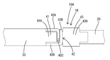
- the support portion 42 supports the rising portion 41 from behind, as shown in FIGS.
- the support portion 42 includes a first support plate 42A and a second support plate 42B.
- the first support plate 42A extends rearward from the right side plate portion 31 and is bent leftward.
- a rear side portion 42C (a portion bent to the left) of the first support plate 42A faces the rising plate 41B of the rising portion 41 from behind.
- the rear portion 42C of the first support plate 42A is in contact with the rising plate 41B of the rising portion 41 from behind.
- the second support plate 42B extends rearward from the left side plate portion 31 and further bends to the right.
- a rear side portion 42D (a portion bent to the right) of the second support plate 42B faces a rear side portion 42C of the first support plate 42A from behind. Specifically, the rear side portion 42D of the second support plate 42B contacts the rear side portion 42C of the first support plate 42A from behind.
- a tensile force (pulling force that pulls backward) acts on wiring board 20 , rising portion 41 tends to tilt backward, but support portion 42 suppresses the tilting of rising portion 41 .
- the substrate portion 43 corresponds to an example of the "long portion" of the present invention.
- the substrate portion 43 has a double plate structure as shown in FIGS. Therefore, even if the metal plate material of the fixing portion 16 is thin, the double plate structure of the substrate portion 43 can increase the rigidity and improve the fixing strength.
- the substrate portion 43 extends rearward from the upper end of the rising portion 41 (more specifically, the rising plate 41B), bends downward, and extends forward.
- the upper surface of the substrate portion 43 is at the same height as the upper surface of the upper plate portion 32 of the connecting portion 14 .
- the upper surface of the substrate portion 43 is parallel to the upper surface of the upper plate portion 32 . That is, the upper surface of the substrate portion 43 and the upper surface of the upper plate portion 32 are flush with each other.
- the substrate section 43 includes an upper substrate 43A and a lower substrate 43B.
- the upper substrate 43A extends rearward from the upper end of the rising plate 41B.
- the substrate portion 43 is in contact with conductive paths (not shown) of the wiring board 20 .
- the substrate portion 43 is in contact with one surface (lower surface) of the wiring board 20 (base material 22).
- the width of the substrate portion 43 in the left-right direction is smaller than the width of the wiring board 20 in the left-right direction, as shown in FIG.
- the lower substrate 43B is connected to the front end of the upper substrate 43A and extends forward so as to fold over the upper substrate 43A.
- the lower substrate 43B is in contact with the lower surface of the upper substrate 43A.
- the lateral width of the lower substrate 43B is approximately the same as the lateral width of the upper substrate 43A.
- the tip (front end) of the lower substrate 43B faces the rear surface of the rising plate 41B from behind.
- a tip (front end) of the lower substrate 43B is positioned above the support portion 42 .
- the crimped portion 44 corresponds to the "short portion" of the present invention.
- the crimped portion 44 extends from the lower substrate 43B of the substrate portion 43 and surrounds the wiring board 20, as shown in FIGS.
- the crimped portion 44 is in contact with the other surface (upper surface) of the base material 22 of the wiring board 20 .
- the crimped portion 44 bites into the other surface (upper surface) of the base material 22 . Since the crimped portion 44 bites into the other surface (upper surface) of the base material 22 made of resin, the fixing force of the fixing portion 16 to the wiring board 20 is improved. Since the board portion 43 bites into the wiring board 20 shallower than the crimped portion 44, the deformation of the conductive path of the wiring board 20 (the conductive path extending on one surface (lower surface) of the base material 22) is suppressed.
- the crimping portion 44 includes a first crimping plate 44A and a second crimping plate 44B.
- the first crimping plate 44A extends upward from a portion of the right end of the lower substrate 43B, bends leftward, and extends leftward.
- the first crimping plate 44A extends from the center of the right end of the lower substrate 43B in the front-rear direction.
- the left side surface of the base end (lower end) of the first crimping plate 44A is in contact with the right end surface of the base material 22 .
- the tip of the first crimping plate 44A (portion extending leftward) bites into the other surface (upper surface) of the base material 22, as shown in FIGS.
- the second crimping plate 44B extends upward from a part of the left end of the lower substrate 43B, bends to the right and extends to the right.
- the second crimping plate 44B extends from the center in the front-rear direction of the left end of the lower substrate 43B.
- the right side surface of the base end (lower end) of the second crimping plate 44B is in contact with the left end surface of the base material 22 .
- the tip (the portion extending to the right) of the second crimping plate 44B is in contact with the upper surface of the first crimping plate 44A.
- the fixing portion 16 can be fixed to the wiring board 20 while the wiring board 20 is not connected to the connecting portion 14 . That is, after the wiring board 20 is surrounded and fixed by the caulked portion 44, the connecting portion 14 can be connected to the front end portion 24 of the wiring board 20 by soldering, for example. Accordingly, the terminal fitting 10 can be positioned and temporarily held with respect to the wiring board 20 before the terminal fitting 10 is connected to the wiring board 20 . As described above, since the upper surface of the substrate portion 43 and the upper surface of the upper plate portion 32 are flush with each other, it is easy to connect the wiring board 20 to the connection portion 14 after the wiring board 20 is temporarily held by the fixing portion 16 . It's becoming
- the crimped portion 44 bites into the other surface (upper surface) of the base material 22 made of resin, thereby improving the fixing force of the fixing portion 16 to the wiring board 20 . Since the crimped portion 44 cuts into the wiring board 20 more shallowly than the substrate portion 43, deformation of the conductive path is suppressed.
- the solder fillet F is not formed on the wiring board 20 at the connection portion between the wiring board 20 and the connecting portion 14 . contact with the left and right side edges 26 and the arcuate portion 35. Therefore, high connection strength between wiring board 20 and connection portion 14 can be obtained.
- the fixing portion 16 extends from the single plate-like lower plate portion 33, the width dimension is easily ensured.
- the fixing portion 16 includes a support portion 42 that supports the rising portion 41 from behind. Therefore, when a tensile force acts on wiring board 20 , rising portion 41 tends to tilt backward, but support portion 42 suppresses the tilting of rising portion 41 .
- the substrate portion 43 has a double plate structure. Therefore, even if the metal plate material of the fixing portion 16 is thin, the double plate structure of the substrate portion 43 can increase the rigidity and improve the fixing strength.
- the connecting portion 14 is connected to the front end portion 24 of the wiring board 20 by soldering, but it may be connected by other methods (such as welding such as ultrasonic welding).
- the substrate portion 43 has a double-plate structure in the first embodiment, it may be configured as a single plate.
- the support portion 42 includes the first support plate 42A and the second support plate 42B, but only one of them may be provided. That is, one supporting plate may support the rising portion 41 from behind.
- the crimping portion 44 includes the first crimping plate 44A and the second crimping plate 44B, but only one of them may be provided. That is, one crimping plate may surround the wiring board 20 and bite into the other surface (upper surface) of the base material 22 .
Landscapes
- Coupling Device And Connection With Printed Circuit (AREA)
- Multi-Conductor Connections (AREA)
Abstract
Description
フレキシブルプリント配線板の前端部に接続される接続部と、
後端部において、前記接続部よりも後方に位置し、前記フレキシブルプリント配線板に固着された固着部と、
を備える。
最初に本開示の実施形態を列記して説明する。
本開示の端子金具は、
(1)フレキシブルプリント配線板の前端部に接続される接続部と、
後端部において、前記接続部よりも後方に位置し、前記フレキシブルプリント配線板に固着された固着部と、
を備える。
本開示の構成によれば、フレキシブルプリント配線板が後方へ引っ張られると、引張力は固着部を介して端子金具全体に作用する。そのため、引張力は、接続部とフレキシブルプリント配線板との接続部分に及ぶことを抑制することができる。よって、フレキシブルプリント配線板が接続部から離脱することを抑制することができる。
[実施例1]
本開示の端子金具を具体化した実施例1を、図1~図8を参照して説明する。本実施例1において、上下の方向については、図1~図3、図6~図8にあらわれる向きを、そのまま上方、下方と定義する。前後の方向については、図2~図6にあらわれる左方、右方を、それぞれ前方、後方と定義する。左右の方向は、図1にあらわれる前方、後方を、それぞれ左方、右方と定義する。
図1、図2に示す本実施例1の端子金具10は、フレキシブルプリント配線板(以下、単に配線板ともいう)20に接続されている。配線板20は、樹脂製の基材22の一面(下面)に導電路(図示略)を延設して構成されている。基材22は、例えば、絶縁樹脂製のシートによって構成されている。導電路は、例えば銅箔によって構成されている。配線板20は、例えば、コネクタハウジング(図示略)に組み付けられて、コネクタ(図示略)を構成する。
以上のように、本開示の端子金具10によれば、フレキシブルプリント配線板20が後方へ引っ張られると、引張力は固着部16を介して端子金具10全体に作用する。そのため、引張力は、接続部14と配線板20との接続部分に及ぶことを抑制することができる。よって、配線板20が接続部14から離脱することを抑制することができる。
本発明は、上記記述及び図面によって説明した実施例に限定されるものではなく、請求の範囲によって示される。本発明には、請求の範囲と均等の意味及び請求の範囲内でのすべての変更が含まれ、下記のような実施形態も含まれることが意図される。
上記実施例1において、接続部14は、はんだ付けによって配線板20の前端部24に接続される例を示したが、その他の方法(超音波溶接等の溶接等)によって接続されてもよい。
上記実施例1において、基板部43は、二重板構造であったが、一枚板として構成されていてもよい。
上記実施例1において、支持部42は、第1支持板42Aと、第2支持板42Bと、を具備していたが、一方のみが設けられていてもよい。すなわち、一方の支持板で立上り部41を後方から支える構成としてもよい。
上記実施例1において、カシメ部44は、第1カシメ板44Aと、第2カシメ板44Bと、を具備していたが、一方のみが設けられていてもよい。すなわち、一方のカシメ板が、配線板20を包囲して、基材22の他面(上面)に食い込む構成としてもよい。
10A…後端部
12…本体部
12A…第1突部
12B…第2突部
14…接続部
16…固着部
20…フレキシブルプリント配線板(配線板)
22…基材
24…前端部
26…左右両側縁
31…側板部
32…上板部
33…下板部
34…接続用板部
35…弧状部
41…立上り部
41A…基端板
41B…立上り板
42…支持部
42A…第1支持板
42B…第2支持板
42C…後側部
42D…後側部
43…基板部
43A…上基板
43B…下基板
44…カシメ部
44A…第1カシメ板
44B…第2カシメ板
F…フィレット
Claims (5)
- フレキシブルプリント配線板の前端部に接続される接続部と、
後端部において、前記接続部よりも後方に位置し、前記フレキシブルプリント配線板に固着された固着部と、
を備える端子金具。 - 前記フレキシブルプリント配線板は、樹脂製の基材の一面に導電路を延設して構成され、
前記固着部は、
前記導電路に接する長尺部と、
前記基材の他面に接する短尺部と、
を有し、
前記短尺部は、前記基材の他面に食い込む請求項1に記載の端子金具。 - 前記接続部は、一対の側板部と、前記側板部の上端縁に連なる上板部と、前記側板部の下端縁同士を繋ぐ一枚の下板部と、を有し、
前記固着部は、前記下板部から延出し、
前記上板部は、一対の前記側板部から弧状部を介して突出し、突出端同士を突き合わせた一対の接続用板部によって構成され、
一対の前記接続用板部には前記フレキシブルプリント配線板が接続され、
一対の前記弧状部が前記フレキシブルプリント配線板の左右両側縁から外方へ張り出している請求項1又は請求項2に記載の端子金具。 - 前記固着部は、
前記下板部から前記フレキシブルプリント配線板側へ立ち上がる立上り部と、
前記立上り部を後方から支える支持部と、
を有する請求項3に記載の端子金具。 - 前記固着部は、
金属板材からなり、
前記フレキシブルプリント配線板の一面に接する基板部と、
前記基板部から延出して前記フレキシブルプリント配線板を包囲するカシメ部と、
を有し、
前記基板部は、二重板構造である請求項1から請求項4のいずれか一項に記載の端子金具。
Priority Applications (2)
| Application Number | Priority Date | Filing Date | Title |
|---|---|---|---|
| CN202280035424.4A CN117337519A (zh) | 2021-05-26 | 2022-03-23 | 端子零件 |
| US18/290,435 US20240258724A1 (en) | 2021-05-26 | 2022-03-23 | Terminal fitting |
Applications Claiming Priority (2)
| Application Number | Priority Date | Filing Date | Title |
|---|---|---|---|
| JP2021088058A JP7549781B2 (ja) | 2021-05-26 | 2021-05-26 | 端子金具 |
| JP2021-088058 | 2021-05-26 |
Publications (1)
| Publication Number | Publication Date |
|---|---|
| WO2022249689A1 true WO2022249689A1 (ja) | 2022-12-01 |
Family
ID=84229804
Family Applications (1)
| Application Number | Title | Priority Date | Filing Date |
|---|---|---|---|
| PCT/JP2022/013445 Ceased WO2022249689A1 (ja) | 2021-05-26 | 2022-03-23 | 端子金具 |
Country Status (4)
| Country | Link |
|---|---|
| US (1) | US20240258724A1 (ja) |
| JP (1) | JP7549781B2 (ja) |
| CN (1) | CN117337519A (ja) |
| WO (1) | WO2022249689A1 (ja) |
Citations (4)
| Publication number | Priority date | Publication date | Assignee | Title |
|---|---|---|---|---|
| JPH10275642A (ja) * | 1997-03-28 | 1998-10-13 | Denso Corp | フレキシブルプリント基板のターミナル |
| JP2001217028A (ja) * | 2000-01-31 | 2001-08-10 | Yazaki Corp | フラット回路体の分岐接続構造 |
| JP2007103138A (ja) * | 2005-10-03 | 2007-04-19 | Yazaki Corp | 圧着装置 |
| JP2011238522A (ja) * | 2010-05-12 | 2011-11-24 | Sumitomo Wiring Syst Ltd | 圧着端子及びボルト締め端子 |
Family Cites Families (1)
| Publication number | Priority date | Publication date | Assignee | Title |
|---|---|---|---|---|
| JP5930089B1 (ja) * | 2015-02-24 | 2016-06-08 | 第一精工株式会社 | 導電端子 |
-
2021
- 2021-05-26 JP JP2021088058A patent/JP7549781B2/ja active Active
-
2022
- 2022-03-23 CN CN202280035424.4A patent/CN117337519A/zh active Pending
- 2022-03-23 US US18/290,435 patent/US20240258724A1/en active Pending
- 2022-03-23 WO PCT/JP2022/013445 patent/WO2022249689A1/ja not_active Ceased
Patent Citations (4)
| Publication number | Priority date | Publication date | Assignee | Title |
|---|---|---|---|---|
| JPH10275642A (ja) * | 1997-03-28 | 1998-10-13 | Denso Corp | フレキシブルプリント基板のターミナル |
| JP2001217028A (ja) * | 2000-01-31 | 2001-08-10 | Yazaki Corp | フラット回路体の分岐接続構造 |
| JP2007103138A (ja) * | 2005-10-03 | 2007-04-19 | Yazaki Corp | 圧着装置 |
| JP2011238522A (ja) * | 2010-05-12 | 2011-11-24 | Sumitomo Wiring Syst Ltd | 圧着端子及びボルト締め端子 |
Also Published As
| Publication number | Publication date |
|---|---|
| JP7549781B2 (ja) | 2024-09-12 |
| US20240258724A1 (en) | 2024-08-01 |
| JP2022181240A (ja) | 2022-12-08 |
| CN117337519A (zh) | 2024-01-02 |
Similar Documents
| Publication | Publication Date | Title |
|---|---|---|
| US8795007B2 (en) | Terminal fitting | |
| US20140206244A1 (en) | Female terminal | |
| TWM331795U (en) | Electrical contact and electrical connector using the same | |
| TW200805822A (en) | An electrical connector for connecting a flat conductive member | |
| JP4443017B2 (ja) | 接続端子 | |
| CN102972105A (zh) | 表面安装夹 | |
| JP7240616B2 (ja) | コネクタ | |
| US7458848B2 (en) | Connector | |
| WO2022249689A1 (ja) | 端子金具 | |
| CN112602237B (zh) | 连接器 | |
| WO2024053505A1 (ja) | 端子ユニット,雌端子,雄端子 | |
| JP7732791B2 (ja) | メス型端子、コネクタ、端子付き電線、コネクタ付き電線及びワイヤーハーネス | |
| JP4431259B2 (ja) | 接続端子 | |
| JP7530557B2 (ja) | フラットケーブルと端子金具の接続構造 | |
| JP4681350B2 (ja) | 電気接続箱 | |
| JP2013084505A (ja) | 端子金具 | |
| JP4723907B2 (ja) | 電気接続箱 | |
| JP2009224137A (ja) | 端子金具 | |
| JP2024148466A (ja) | コネクタ装置 | |
| JP2013025905A (ja) | 基板用コネクタ | |
| JP2015158991A (ja) | コネクタ | |
| JP7717330B2 (ja) | コネクタ | |
| JP4844131B2 (ja) | 回路構成体および電気接続箱 | |
| TWM335050U (en) | Electrical connector | |
| JP2025001807A (ja) | 雌端子金具 |
Legal Events
| Date | Code | Title | Description |
|---|---|---|---|
| 121 | Ep: the epo has been informed by wipo that ep was designated in this application |
Ref document number: 22810966 Country of ref document: EP Kind code of ref document: A1 |
|
| WWE | Wipo information: entry into national phase |
Ref document number: 18290435 Country of ref document: US |
|
| WWE | Wipo information: entry into national phase |
Ref document number: 202280035424.4 Country of ref document: CN |
|
| NENP | Non-entry into the national phase |
Ref country code: DE |
|
| 122 | Ep: pct application non-entry in european phase |
Ref document number: 22810966 Country of ref document: EP Kind code of ref document: A1 |