WO2022239386A1 - エアロゾル生成装置の電源ユニット - Google Patents
エアロゾル生成装置の電源ユニット Download PDFInfo
- Publication number
- WO2022239386A1 WO2022239386A1 PCT/JP2022/008374 JP2022008374W WO2022239386A1 WO 2022239386 A1 WO2022239386 A1 WO 2022239386A1 JP 2022008374 W JP2022008374 W JP 2022008374W WO 2022239386 A1 WO2022239386 A1 WO 2022239386A1
- Authority
- WO
- WIPO (PCT)
- Prior art keywords
- power supply
- thermistor
- circuit board
- connector
- heater
- Prior art date
Links
- 239000000443 aerosol Substances 0.000 title claims description 100
- 230000002093 peripheral effect Effects 0.000 claims description 8
- 238000002485 combustion reaction Methods 0.000 abstract description 13
- 238000001514 detection method Methods 0.000 description 88
- 238000010438 heat treatment Methods 0.000 description 60
- 101100236764 Caenorhabditis elegans mcu-1 gene Proteins 0.000 description 53
- 239000000758 substrate Substances 0.000 description 21
- 238000010586 diagram Methods 0.000 description 17
- 238000004891 communication Methods 0.000 description 15
- 239000000796 flavoring agent Substances 0.000 description 15
- 235000019634 flavors Nutrition 0.000 description 14
- 125000006850 spacer group Chemical group 0.000 description 8
- 239000003990 capacitor Substances 0.000 description 7
- 230000005540 biological transmission Effects 0.000 description 6
- 241000208125 Nicotiana Species 0.000 description 5
- 235000002637 Nicotiana tabacum Nutrition 0.000 description 5
- 238000007599 discharging Methods 0.000 description 5
- 239000000463 material Substances 0.000 description 5
- DNIAPMSPPWPWGF-UHFFFAOYSA-N Propylene glycol Chemical compound CC(O)CO DNIAPMSPPWPWGF-UHFFFAOYSA-N 0.000 description 3
- 238000003825 pressing Methods 0.000 description 3
- 238000012545 processing Methods 0.000 description 3
- PEDCQBHIVMGVHV-UHFFFAOYSA-N Glycerine Chemical compound OCC(O)CO PEDCQBHIVMGVHV-UHFFFAOYSA-N 0.000 description 2
- 230000005674 electromagnetic induction Effects 0.000 description 2
- 239000000284 extract Substances 0.000 description 2
- 230000006698 induction Effects 0.000 description 2
- 239000011810 insulating material Substances 0.000 description 2
- 238000000034 method Methods 0.000 description 2
- 238000012986 modification Methods 0.000 description 2
- 230000004048 modification Effects 0.000 description 2
- 238000004904 shortening Methods 0.000 description 2
- NOOLISFMXDJSKH-UTLUCORTSA-N (+)-Neomenthol Chemical compound CC(C)[C@@H]1CC[C@@H](C)C[C@@H]1O NOOLISFMXDJSKH-UTLUCORTSA-N 0.000 description 1
- NOOLISFMXDJSKH-UHFFFAOYSA-N DL-menthol Natural products CC(C)C1CCC(C)CC1O NOOLISFMXDJSKH-UHFFFAOYSA-N 0.000 description 1
- 241000196324 Embryophyta Species 0.000 description 1
- HBBGRARXTFLTSG-UHFFFAOYSA-N Lithium ion Chemical compound [Li+] HBBGRARXTFLTSG-UHFFFAOYSA-N 0.000 description 1
- 235000014435 Mentha Nutrition 0.000 description 1
- 241001072983 Mentha Species 0.000 description 1
- 230000002159 abnormal effect Effects 0.000 description 1
- 230000004308 accommodation Effects 0.000 description 1
- 239000000919 ceramic Substances 0.000 description 1
- 239000000470 constituent Substances 0.000 description 1
- 230000007423 decrease Effects 0.000 description 1
- 239000003792 electrolyte Substances 0.000 description 1
- 239000008151 electrolyte solution Substances 0.000 description 1
- 235000013355 food flavoring agent Nutrition 0.000 description 1
- 239000011245 gel electrolyte Substances 0.000 description 1
- 235000011187 glycerol Nutrition 0.000 description 1
- 241000411851 herbal medicine Species 0.000 description 1
- 235000008216 herbs Nutrition 0.000 description 1
- 239000002608 ionic liquid Substances 0.000 description 1
- WABPQHHGFIMREM-UHFFFAOYSA-N lead(0) Chemical compound [Pb] WABPQHHGFIMREM-UHFFFAOYSA-N 0.000 description 1
- 239000007788 liquid Substances 0.000 description 1
- 229910001416 lithium ion Inorganic materials 0.000 description 1
- 229940041616 menthol Drugs 0.000 description 1
- 235000014569 mints Nutrition 0.000 description 1
- 229930014626 natural product Natural products 0.000 description 1
- 239000002304 perfume Substances 0.000 description 1
- 230000001681 protective effect Effects 0.000 description 1
- 230000000391 smoking effect Effects 0.000 description 1
- 239000007787 solid Substances 0.000 description 1
- 239000007784 solid electrolyte Substances 0.000 description 1
- 150000005846 sugar alcohols Polymers 0.000 description 1
- 238000012546 transfer Methods 0.000 description 1
- XLYOFNOQVPJJNP-UHFFFAOYSA-N water Substances O XLYOFNOQVPJJNP-UHFFFAOYSA-N 0.000 description 1
Images


Classifications
-
- H—ELECTRICITY
- H05—ELECTRIC TECHNIQUES NOT OTHERWISE PROVIDED FOR
- H05B—ELECTRIC HEATING; ELECTRIC LIGHT SOURCES NOT OTHERWISE PROVIDED FOR; CIRCUIT ARRANGEMENTS FOR ELECTRIC LIGHT SOURCES, IN GENERAL
- H05B3/00—Ohmic-resistance heating
- H05B3/02—Details
- H05B3/04—Waterproof or air-tight seals for heaters
-
- A—HUMAN NECESSITIES
- A24—TOBACCO; CIGARS; CIGARETTES; SIMULATED SMOKING DEVICES; SMOKERS' REQUISITES
- A24F—SMOKERS' REQUISITES; MATCH BOXES; SIMULATED SMOKING DEVICES
- A24F40/00—Electrically operated smoking devices; Component parts thereof; Manufacture thereof; Maintenance or testing thereof; Charging means specially adapted therefor
- A24F40/40—Constructional details, e.g. connection of cartridges and battery parts
- A24F40/46—Shape or structure of electric heating means
-
- A—HUMAN NECESSITIES
- A24—TOBACCO; CIGARS; CIGARETTES; SIMULATED SMOKING DEVICES; SMOKERS' REQUISITES
- A24F—SMOKERS' REQUISITES; MATCH BOXES; SIMULATED SMOKING DEVICES
- A24F40/00—Electrically operated smoking devices; Component parts thereof; Manufacture thereof; Maintenance or testing thereof; Charging means specially adapted therefor
- A24F40/40—Constructional details, e.g. connection of cartridges and battery parts
-
- A—HUMAN NECESSITIES
- A24—TOBACCO; CIGARS; CIGARETTES; SIMULATED SMOKING DEVICES; SMOKERS' REQUISITES
- A24F—SMOKERS' REQUISITES; MATCH BOXES; SIMULATED SMOKING DEVICES
- A24F40/00—Electrically operated smoking devices; Component parts thereof; Manufacture thereof; Maintenance or testing thereof; Charging means specially adapted therefor
- A24F40/50—Control or monitoring
- A24F40/51—Arrangement of sensors
-
- H—ELECTRICITY
- H02—GENERATION; CONVERSION OR DISTRIBUTION OF ELECTRIC POWER
- H02J—CIRCUIT ARRANGEMENTS OR SYSTEMS FOR SUPPLYING OR DISTRIBUTING ELECTRIC POWER; SYSTEMS FOR STORING ELECTRIC ENERGY
- H02J7/00—Circuit arrangements for charging or depolarising batteries or for supplying loads from batteries
- H02J7/007—Regulation of charging or discharging current or voltage
- H02J7/007188—Regulation of charging or discharging current or voltage the charge cycle being controlled or terminated in response to non-electric parameters
- H02J7/007192—Regulation of charging or discharging current or voltage the charge cycle being controlled or terminated in response to non-electric parameters in response to temperature
-
- H—ELECTRICITY
- H05—ELECTRIC TECHNIQUES NOT OTHERWISE PROVIDED FOR
- H05B—ELECTRIC HEATING; ELECTRIC LIGHT SOURCES NOT OTHERWISE PROVIDED FOR; CIRCUIT ARRANGEMENTS FOR ELECTRIC LIGHT SOURCES, IN GENERAL
- H05B1/00—Details of electric heating devices
- H05B1/02—Automatic switching arrangements specially adapted to apparatus ; Control of heating devices
- H05B1/0202—Switches
-
- H—ELECTRICITY
- H05—ELECTRIC TECHNIQUES NOT OTHERWISE PROVIDED FOR
- H05B—ELECTRIC HEATING; ELECTRIC LIGHT SOURCES NOT OTHERWISE PROVIDED FOR; CIRCUIT ARRANGEMENTS FOR ELECTRIC LIGHT SOURCES, IN GENERAL
- H05B1/00—Details of electric heating devices
- H05B1/02—Automatic switching arrangements specially adapted to apparatus ; Control of heating devices
- H05B1/0227—Applications
- H05B1/023—Industrial applications
- H05B1/0244—Heating of fluids
-
- H—ELECTRICITY
- H05—ELECTRIC TECHNIQUES NOT OTHERWISE PROVIDED FOR
- H05B—ELECTRIC HEATING; ELECTRIC LIGHT SOURCES NOT OTHERWISE PROVIDED FOR; CIRCUIT ARRANGEMENTS FOR ELECTRIC LIGHT SOURCES, IN GENERAL
- H05B3/00—Ohmic-resistance heating
- H05B3/0019—Circuit arrangements
-
- H—ELECTRICITY
- H05—ELECTRIC TECHNIQUES NOT OTHERWISE PROVIDED FOR
- H05B—ELECTRIC HEATING; ELECTRIC LIGHT SOURCES NOT OTHERWISE PROVIDED FOR; CIRCUIT ARRANGEMENTS FOR ELECTRIC LIGHT SOURCES, IN GENERAL
- H05B6/00—Heating by electric, magnetic or electromagnetic fields
- H05B6/02—Induction heating
- H05B6/06—Control, e.g. of temperature, of power
-
- H—ELECTRICITY
- H05—ELECTRIC TECHNIQUES NOT OTHERWISE PROVIDED FOR
- H05B—ELECTRIC HEATING; ELECTRIC LIGHT SOURCES NOT OTHERWISE PROVIDED FOR; CIRCUIT ARRANGEMENTS FOR ELECTRIC LIGHT SOURCES, IN GENERAL
- H05B6/00—Heating by electric, magnetic or electromagnetic fields
- H05B6/02—Induction heating
- H05B6/10—Induction heating apparatus, other than furnaces, for specific applications
- H05B6/105—Induction heating apparatus, other than furnaces, for specific applications using a susceptor
- H05B6/108—Induction heating apparatus, other than furnaces, for specific applications using a susceptor for heating a fluid
-
- A—HUMAN NECESSITIES
- A24—TOBACCO; CIGARS; CIGARETTES; SIMULATED SMOKING DEVICES; SMOKERS' REQUISITES
- A24F—SMOKERS' REQUISITES; MATCH BOXES; SIMULATED SMOKING DEVICES
- A24F40/00—Electrically operated smoking devices; Component parts thereof; Manufacture thereof; Maintenance or testing thereof; Charging means specially adapted therefor
- A24F40/20—Devices using solid inhalable precursors
-
- H—ELECTRICITY
- H05—ELECTRIC TECHNIQUES NOT OTHERWISE PROVIDED FOR
- H05B—ELECTRIC HEATING; ELECTRIC LIGHT SOURCES NOT OTHERWISE PROVIDED FOR; CIRCUIT ARRANGEMENTS FOR ELECTRIC LIGHT SOURCES, IN GENERAL
- H05B2203/00—Aspects relating to Ohmic resistive heating covered by group H05B3/00
- H05B2203/02—Heaters using heating elements having a positive temperature coefficient
-
- H—ELECTRICITY
- H05—ELECTRIC TECHNIQUES NOT OTHERWISE PROVIDED FOR
- H05B—ELECTRIC HEATING; ELECTRIC LIGHT SOURCES NOT OTHERWISE PROVIDED FOR; CIRCUIT ARRANGEMENTS FOR ELECTRIC LIGHT SOURCES, IN GENERAL
- H05B2203/00—Aspects relating to Ohmic resistive heating covered by group H05B3/00
- H05B2203/021—Heaters specially adapted for heating liquids
-
- H—ELECTRICITY
- H05—ELECTRIC TECHNIQUES NOT OTHERWISE PROVIDED FOR
- H05B—ELECTRIC HEATING; ELECTRIC LIGHT SOURCES NOT OTHERWISE PROVIDED FOR; CIRCUIT ARRANGEMENTS FOR ELECTRIC LIGHT SOURCES, IN GENERAL
- H05B2203/00—Aspects relating to Ohmic resistive heating covered by group H05B3/00
- H05B2203/022—Heaters specially adapted for heating gaseous material
Definitions
- the present invention relates to a power supply unit for an aerosol generator.
- Patent Documents 1 and 2 describe a power supply unit for an aerosol generator configured so that the state of the device can be grasped from a thermistor provided in the housing. From the viewpoint of improving accuracy, the thermistor is preferably arranged as close as possible to the object to be measured. Therefore, the thermistor is connected to the circuit board via wiring and connectors. On the other hand, as the aerosol generating device becomes more sophisticated, there are cases where a plurality of circuit boards are provided in the device.
- the present invention provides a power supply unit for an aerosol generator in which thermistor connectors are appropriately arranged for a plurality of circuit boards.
- the power supply unit of the aerosol generator of the present invention comprises: a power supply; a heater connector connected to a heater that consumes power supplied from the power supply to heat the aerosol source; a thermistor; a thermistor connector to which the thermistor is connected; a first circuit board; A second circuit board separate from the first circuit board, The heater connector is arranged on the second circuit board out of the first circuit board and the second circuit board, The number of the thermistor connectors arranged on the first circuit board is greater than the number of the thermistor connectors arranged on the second circuit board.
- the present invention it is possible to appropriately arrange thermistor connectors on a plurality of circuit boards, and improve the thermistor detection accuracy.
- FIG. 1 is a perspective view of a non-combustion inhaler
- FIG. 1 is a perspective view of a non-combustion inhaler showing a state in which a rod is attached
- FIG. Fig. 10 is another perspective view of a non-combustion type inhaler
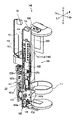
- 1 is an exploded perspective view of a non-combustion inhaler
- FIG. Fig. 3 is a perspective view of the internal unit of the non-combustion inhaler
- FIG. 6 is an exploded perspective view of the internal unit of FIG. 5
- FIG. 3 is a perspective view of the internal unit with the power supply and chassis removed
- FIG. 11 is another perspective view of the internal unit with the power supply and chassis removed
- It is a schematic diagram for demonstrating the operation mode of an aspirator.
- FIG. 4 is a diagram for explaining the operation of an electric circuit in sleep mode; It is a figure for demonstrating the operation
- FIG. 4 is a diagram for explaining the operation of the electric circuit in the heating initial setting mode; It is a figure for demonstrating the operation
- FIG. 5 is a diagram for explaining the operation of the electric circuit when detecting the temperature of the heater in the heating mode;
- FIG. 4 is a diagram for explaining the operation of the electric circuit in charging mode; It is a figure which shows the main surface of a receptacle mounting board.
- FIG. 3 is a cross-sectional view of the non-combustion aspirator taken in a horizontal plane through a thermistor located near the heater;
- FIG. 22 is a cross-sectional view of the non-combustion aspirator taken through a phantom plane indicated by AA in FIG. 21;
- suction system which is one embodiment of the aerosol generator of the present invention, will be described below with reference to the drawings.
- This suction system includes a non-combustion type suction device 100 (hereinafter also simply referred to as "suction device 100"), which is an embodiment of the power supply unit of the present invention, and a rod 500 heated by the suction device 100.
- suction device 100 a non-combustion type suction device 100
- the suction device 100 accommodates the heating unit in a non-detachable manner
- the heating unit may be detachably attached to the aspirator 100 .
- the rod 500 and the heating unit may be integrated and detachably attached to the aspirator 100 .
- the power supply unit of the aerosol generator may have a configuration that does not include the heating section as a component.
- “non-detachable” refers to a mode in which detachment is not possible as far as the intended use is concerned.
- an induction heating coil provided in the aspirator 100 and a susceptor built in the rod 500 may cooperate to form a heating unit.
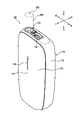
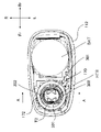
- FIG. 1 is a perspective view showing the overall configuration of the aspirator 100.
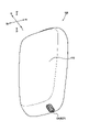
- FIG. FIG. 2 is a perspective view of the suction device 100 showing a state in which the rod 500 is attached.
- FIG. 3 is another perspective view of the suction device 100.
- FIG. FIG. 4 is an exploded perspective view of the aspirator 100.
- FIG. Also, in the following description, for the sake of convenience, the orthogonal coordinate system of a three-dimensional space is used, in which the three mutually orthogonal directions are the front-back direction, the left-right direction, and the up-down direction. In the figure, the front is indicated by Fr, the rear by Rr, the right by R, the left by L, the upper by U, and the lower by D.
- the inhaler 100 generates flavor-containing aerosol by heating an elongated, substantially cylindrical rod 500 (see FIG. 2) as an example of a flavor component-generating base having a filling containing an aerosol source and a flavor source. configured to
- Rod 500 includes a fill containing an aerosol source that is heated at a predetermined temperature to produce an aerosol.
- the type of aerosol source is not particularly limited, and extracts from various natural products and/or their constituent components can be selected according to the application.
- the aerosol source may be solid or liquid, for example polyhydric alcohols such as glycerin, propylene glycol, or water.
- the aerosol source may include a flavor source such as a tobacco material or an extract derived from the tobacco material that releases flavor components upon heating.
- the gas to which the flavor component is added is not limited to an aerosol, and for example an invisible vapor may be generated.
- the filling of rod 500 may contain tobacco shreds as a flavor source.
- Materials for shredded tobacco are not particularly limited, and known materials such as lamina and backbone can be used.
- the filling may contain one or more perfumes.
- the type of flavoring agent is not particularly limited, but menthol is preferable from the viewpoint of imparting a good smoking taste.
- Flavor sources may contain plants other than tobacco, such as mints, herbal medicines, or herbs. Depending on the application, rod 500 may not contain a flavor source.
- the suction device 100 includes a substantially rectangular parallelepiped case 110 having a front surface, a rear surface, a left surface, a right surface, an upper surface, and a lower surface.
- the case 110 comprises a bottomed cylindrical case body 112 in which front, rear, top, bottom, and right surfaces are integrally formed, and a left surface that seals an opening 114 (see FIG. 4) of the case body 112. It has an outer panel 115 , an inner panel 118 , and a slider 119 .
- the inner panel 118 is fixed to the case body 112 with bolts 120 .
- the outer panel 115 is fixed to the case body 112 so as to cover the outer surface of the inner panel 118 by a magnet 124 held by a chassis 150 (see FIG. 5) housed in the case body 112 and described later. Since the outer panel 115 is fixed by the magnet 124, the user can replace the outer panel 115 according to his or her preference.
- the inner panel 118 is provided with two through holes 126 through which the magnets 124 pass.
- the inner panel 118 is further provided with a longitudinally elongated hole 127 and a circular round hole 128 between the two vertically arranged through holes 126 .
- This long hole 127 is for transmitting light emitted from eight LEDs (Light Emitting Diodes) L1 to L8 built in the case body 112 .
- a button-type operation switch OPS built in the case body 112 passes through the round hole 128 . Thereby, the user can detect the light emitted from the eight LEDs L1 to L8 through the LED window 116 of the outer panel 115. FIG. Also, the user can press down the operation switch OPS via the pressing portion 117 of the outer panel 115 .
- the upper surface of the case body 112 is provided with an opening 132 into which the rod 500 can be inserted.
- the slider 119 is coupled to the case body 112 so as to be movable in the front-rear direction between a position for closing the opening 132 (see FIG. 1) and a position for opening the opening 132 (see FIG. 2). It should be noted that in FIG. 2, the slider 119 is transparent and only the outer shape of the slider 119 is indicated by a chain double-dashed line for easy understanding.
- the operation switch OPS is used to perform various operations of the aspirator 100.
- the user operates the operation switch OPS via the pressing portion 117 while inserting the rod 500 into the opening 132 as shown in FIG.
- the heating unit 170 (see FIG. 5) heats the rod 500 without burning it.
- an aerosol is generated from the aerosol source contained in the rod 500 and the flavor of the flavor source contained in the rod 500 is added to the aerosol.
- the user can inhale the flavor-containing aerosol by holding the mouthpiece 502 of the rod 500 projecting from the opening 132 and inhaling.
- a charging terminal 134 is provided for receiving power supply by being electrically connected to an external power source such as an outlet or a mobile battery.
- the charging terminal 134 is a USB (Universal Serial Bus) Type-C receptacle, but is not limited to this.
- Charging terminal 134 is hereinafter also referred to as receptacle RCP.
- the charging terminal 134 may include, for example, a power receiving coil and be configured to be capable of contactlessly receiving power transmitted from an external power supply.
- the wireless power transfer method in this case may be an electromagnetic induction type, a magnetic resonance type, or a combination of the electromagnetic induction type and the magnetic resonance type.
- the charging terminal 134 can be connected to various USB terminals or the like, and may have the power receiving coil described above.
- the configuration of the aspirator 100 shown in FIGS. 1-4 is merely an example.
- the inhaler 100 holds the rod 500 and applies an action such as heating to generate gas to which a flavor component is added from the rod 500, and the user can inhale the generated gas. It can be configured in various forms.
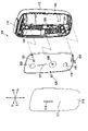
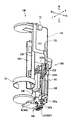
- FIG. 5 is a perspective view of the internal unit 140 of the suction device 100.
- FIG. 6 is an exploded perspective view of the internal unit 140 of FIG. 5.
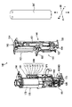
- FIG. 7 is a perspective view of internal unit 140 with power supply BAT and chassis 150 removed.
- FIG. 8 is another perspective view of the internal unit 140 with the power supply BAT and chassis 150 removed.
- the internal unit 140 housed in the internal space of the case 110 includes a chassis 150, a power supply BAT, a circuit section 160, a heating section 170, a notification section 180, and various sensors.
- the chassis 150 includes a plate-shaped chassis body 151 arranged substantially in the center of the interior space of the case 110 in the front-rear direction and extending in the vertical and front-rear directions, and a chassis body 151 disposed substantially in the center of the interior space of the case 110 in the front-rear direction.
- a plate-shaped front and rear dividing wall 152 extending in the vertical and horizontal directions
- a plate-shaped upper and lower dividing wall 153 extending forward from substantially the center of the front and rear dividing wall 152 in the vertical direction
- the front and rear dividing wall 152 and the upper edges of the chassis body 151 and a plate-shaped chassis lower wall 155 extending rearward from the front-rear dividing wall 152 and the lower edge of the chassis body 151 .
- the left surface of the chassis body 151 is covered with the inner panel 118 and the outer panel 115 of the case 110 described above.
- the internal space of the case 110 is defined by a chassis 150 such that a heating unit housing area 142 is defined in the upper front, a board housing area 144 is defined in the lower front, and a power supply housing space 146 is defined in the rear to extend vertically. ing.
- the heating part 170 housed in the heating part housing area 142 is composed of a plurality of tubular members, which are concentrically arranged to form a tubular body as a whole.
- the heating section 170 has a rod housing section 172 capable of housing a portion of the rod 500 therein, and a heater HTR (see FIGS. 10 to 16) that heats the rod 500 from its outer circumference or center.
- the surface of the rod housing portion 172 and the heater HTR are insulated by forming the rod housing portion 172 from a heat insulating material or providing a heat insulating material inside the rod housing portion 172 .
- the heater HTR may be any element that can heat the rod 500 .
- the heater HTR is, for example, a heating element.
- Heating elements include heating resistors, ceramic heaters, induction heaters, and the like.
- the heater HTR for example, one having a PTC (Positive Temperature Coefficient) characteristic in which the resistance value increases as the temperature increases is preferably used.
- a heater HTR having NTC (Negative Temperature Coefficient) characteristics in which the resistance value decreases as the temperature increases may be used.
- the heating part 170 has a function of defining a flow path of air to be supplied to the rod 500 and a function of heating the rod 500 .
- the case 110 is formed with a vent (not shown) for introducing air, and is configured to allow air to enter the heating unit 170 .
- the power supply BAT housed in the power supply housing space 146 is a rechargeable secondary battery, an electric double layer capacitor, or the like, preferably a lithium ion secondary battery.
- the electrolyte of the power supply BAT may be composed of one or a combination of a gel electrolyte, an electrolytic solution, a solid electrolyte, and an ionic liquid.
- the notification unit 180 notifies various information such as the SOC (State Of Charge) indicating the state of charge of the power supply BAT, the preheating time during suction, and the suction possible period.
- the notification unit 180 of this embodiment includes eight LEDs L1 to L8 and a vibration motor M.
- the notification unit 180 may be composed of light emitting elements such as LEDs L1 to L8, may be composed of vibrating elements such as the vibration motor M, or may be composed of sound output elements.
- the notification unit 180 may be a combination of two or more elements selected from the light emitting element, the vibration element, and the sound output element.
- Various sensors include an intake air sensor that detects the user's puff action (sucking action), a power supply temperature sensor that detects the temperature of the power supply BAT, a heater temperature sensor that detects the temperature of the heater HTR, and a case temperature sensor that detects the temperature of the case 110. , a cover position sensor that detects the position of the slider 119, a panel detection sensor that detects attachment/detachment of the outer panel 115, and the like.
- the intake sensor is mainly composed of a thermistor T2 arranged near the opening 132, for example.
- the power supply temperature sensor is mainly composed of, for example, a thermistor T1 arranged near the power supply BAT.
- the heater temperature sensor is mainly composed of, for example, a thermistor T3 arranged near the heater HTR.
- the rod housing portion 172 is preferably insulated from the heater HTR.
- the thermistor T3 is preferably in contact with or close to the heater HTR inside the rod housing portion 172 . If the heater HTR has PTC characteristics or NTC characteristics, the heater HTR itself may be used as the heater temperature sensor.
- the case temperature sensor is mainly composed of, for example, a thermistor T4 arranged near the left surface of the case 110 .
- the cover position sensor is mainly composed of a Hall IC 14 (see FIGS. 10 to 16) including a Hall element arranged near the slider 119 .
- the panel detection sensor mainly includes a Hall IC 13 (see FIGS. 10 to 16) including a Hall element arranged near the inner surface of the inner panel 118 .
- the circuit section 160 includes four circuit boards, multiple ICs (Integrate Circuits), and multiple elements.
- the four circuit boards are an MCU-mounted board 161 on which an MCU (Micro Controller Unit) 1 and a charging IC 2, which will be described later, are mainly arranged, a receptacle-mounted board 162 mainly on which charging terminals 134 are arranged, an operation switch OPS, and an LED An LED mounting substrate 163 on which L1 to L8 and a communication IC 15 described later are arranged, and a Hall IC mounting substrate 164 on which a Hall IC 14 including a Hall element constituting a cover position sensor is arranged.
- the MCU mounting board 161 and the receptacle mounting board 162 are arranged parallel to each other in the board accommodation area 144 . More specifically, the MCU mounting board 161 and the receptacle mounting board 162 are arranged such that their element mounting surfaces are arranged along the horizontal direction and the vertical direction, and the MCU mounting board 161 is arranged in front of the receptacle mounting board 162. .
- the MCU mounting board 161 and the receptacle mounting board 162 are provided with openings 175 and 176 (see FIGS. 17 to 20), respectively.
- the MCU mounting board 161 and the receptacle mounting board 162 are fixed to the chassis 150 with bolts 136 with a cylindrical spacer 173 having a through hole interposed between the peripheral edges 166 and 168 of the openings 175 and 176. be done.
- the bolt 136 is inserted through the opening 175 of the MCU mounting board 161, the through hole of the cylindrical spacer 173, and the opening 176 of the receptacle mounting board 162, so that the MCU mounting board 161, the receptacle mounting board 162 and the power source BAT are inserted in the front-rear direction.
- the spacer 173 is fixed to the substrate fixing portion 156 of the front-rear dividing wall 152 arranged between them. Thereby, the MCU mounting board 161 and the receptacle mounting board 162 are held in parallel by the spacers 173 .
- the spacer 173 has conductivity, and the grounds of the MCU mounting board 161 and the receptacle mounting board 162 are connected via the spacer 173 .
- the ground potentials of the MCU-mounted substrate 161 and the receptacle-mounted substrate 162 can be aligned, and the supply of charging power and operating power and communication between the MCU-mounted substrate 161 and the receptacle-mounted substrate 162 can be stabilized. can.
- the MCU mounting board 161 and the receptacle mounting board 162 have main surfaces 161a and 162a that face forward, and secondary surfaces 161b and 162b that are opposite to the main surfaces 161a and 162a. and the main surface 162a of the receptacle mounting board 162 face each other with a predetermined gap SP therebetween.
- a main surface 161 a of the MCU mounting board 161 faces the front surface of the case 110
- a secondary surface 162 b of the receptacle mounting board 162 faces the front and rear dividing walls 152 of the chassis 150 .
- the MCU mounting board 161 and the receptacle mounting board 162 are electrically connected via a flexible wiring board 165 .
- a flexible wiring board 165 that electrically connects the MCU mounting board 161 and the receptacle mounting board 162 connects the FPC connection portions 231 and 232 of the MCU mounting board 161 and the receptacle mounting board 162 (see FIGS. 17 to 20). Elements and ICs mounted on the MCU mounting board 161 and the receptacle mounting board 162 will be described later.
- the LED mounting board 163 is arranged on the left side of the chassis body 151 and between the two magnets 124 arranged vertically.
- the element mounting surface of the LED mounting substrate 163 is arranged along the vertical direction and the front-rear direction.
- the element mounting surfaces of the MCU mounting board 161 and the receptacle mounting board 162 are orthogonal to the element mounting surface of the LED mounting board 163 .
- the element mounting surfaces of the MCU mounting board 161 and the receptacle mounting board 162 and the element mounting surface of the LED mounting board 163 are not limited to being orthogonal, but preferably intersect (non-parallel).
- the vibration motor M which forms the notification unit 180 together with the LEDs L1 to L8, is fixed to the bottom surface of the chassis bottom wall 155 and electrically connected to the MCU mounting board 161.
- the Hall IC mounting board 164 is arranged on the upper surface of the chassis upper wall 154 .
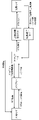
- FIG. 9 is a schematic diagram for explaining the operation modes of the aspirator 100.
- the operating modes of the suction device 100 include charging mode, sleep mode, active mode, heating initialization mode, heating mode, and heating termination mode.
- the sleep mode is a mode for saving power by stopping the power supply to the electrical parts mainly required for heating control of the heater HTR.
- the active mode is a mode in which most functions except heating control of the heater HTR are enabled.
- the operation mode is switched to the active mode.
- the slider 119 is closed or the non-operating time of the operation switch OPS reaches a predetermined time while the aspirator 100 is operating in the active mode, the operating mode is switched to the sleep mode.
- the heating initial setting mode is a mode for initializing control parameters and the like for starting heating control of the heater HTR.
- the aspirator 100 detects the operation of the operation switch OPS while operating in the active mode, it switches the operation mode to the heating initial setting mode, and when the initial setting is completed, switches the operation mode to the heating mode.
- the heating mode is a mode that executes heating control of the heater HTR (heating control for aerosol generation and heating control for temperature detection).
- the aspirator 100 starts heating control of the heater HTR when the operation mode is switched to the heating mode.
- the heating end mode is a mode for executing heating control end processing (heating history storage processing, etc.) of the heater HTR.
- the operation mode is switched to the heating end mode.
- the operation mode is switched to the active mode.
- the USB connection is established while the aspirator 100 is operating in the heating mode, the operating mode is switched to the heating end mode, and when the end processing is completed, the operating mode is switched to the charging mode. As shown in FIG.
- the operating mode may be switched to the active mode before switching the operating mode to the charging mode.
- the aspirator 100 may switch the operation mode in order of the heating end mode, the active mode, and the charging mode when the USB connection is made while operating in the heating mode.
- the charging mode is a mode in which the power supply BAT is charged with power supplied from an external power supply connected to the receptacle RCP.
- the aspirator 100 switches the operation mode to the charge mode when an external power source is connected (USB connection) to the receptacle RCP while operating in sleep mode or active mode.
- the aspirator 100 switches the operation mode to the sleep mode when the charging of the power supply BAT is completed or the connection between the receptacle RCP and the external power supply is released while operating in the charging mode.
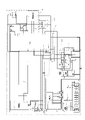
- FIG. 10 is a diagram showing a schematic configuration of an electric circuit of the internal unit 140. As shown in FIG. Note that FIG. 10 shows only main elements and an IC.
- the wiring indicated by the thick solid line in FIG. 10 is the wiring (the wiring connected to the ground provided in the internal unit 140) that has the same potential as the reference potential (ground potential) of the internal unit 140. It is described as a ground line below.
- an electric component in which a plurality of circuit elements are chipped is indicated by a rectangle, and the symbols of various terminals are indicated inside the rectangle.
- a power supply terminal VCC and a power supply terminal VDD mounted on the chip indicate power supply terminals on the high potential side, respectively.
- a power supply terminal VSS and a ground terminal GND mounted on the chip indicate power supply terminals on the low potential side (reference potential side).
- the power supply voltage is the difference between the potential of the power supply terminal on the high potential side and the potential of the power supply terminal on the low potential side. Chipped electrical components use this power supply voltage to perform various functions.
- the MCU-mounted board 161 is configured by combining, as main electrical components, an MCU 1 that controls the entire sucker 100, a charging IC 2 that controls charging of the power source BAT, a capacitor, a resistor, a transistor, and the like.
- a load switch (hereinafter referred to as LSW) 3 and a voltage dividing circuit Pc for USB connection detection are provided.
- a ground terminal GND of each of the charging IC2 and LSW3 is connected to a ground line.
- the LED mounting board 163 is provided with, as main electrical components, a Hall IC 13 including a Hall element that constitutes a panel detection sensor, LEDs L1 to L8, an operation switch OPS, and a communication IC 15.
- the communication IC 15 is a communication module for communicating with electronic devices such as smartphones.
- a power supply terminal VSS of the Hall IC 13 and a ground terminal GND of the communication IC 15 are each connected to a ground line.
- Communication IC 15 and MCU 1 are configured to be communicable via communication line LN.
- One end of the operation switch OPS is connected to the ground line, and the other end of the operation switch OPS is connected to the terminal P4 of the MCU1.
- the receptacle mounting board 162 includes, as main electrical components, a power connector electrically connected to the power source BAT (in the figure, the power source BAT connected to this power connector is shown), and a step-up DC/DC converter 9 ( ), a protection IC 10, an overvoltage protection IC 11, a receptacle RCP, switches S3 and S4 composed of MOSFETs, an operational amplifier OP1, and a pair electrically connected to a heater HTR ( A heater connector Cn on the positive electrode side and the negative electrode side) is provided.
- the two ground terminals GND of the receptacle RCP, the ground terminal GND of the step-up DC/DC converter 9, the power supply terminal VSS of the protection IC 10, the ground terminal GND of the overvoltage protection IC 11, and the negative power supply terminal of the operational amplifier OP1 are grounded. connected to the line.
- the Hall IC mounting board 164 is provided with a Hall IC 14 including a Hall element that constitutes a cover position sensor.
- a power terminal VSS of the Hall IC 14 is connected to the ground line.
- the output terminal OUT of the Hall IC 14 is connected to the terminal P8 of the MCU1.
- the MCU1 detects opening/closing of the slider 119 from a signal input to the terminal P8.
- the two power supply input terminals V BUS of the receptacle RCP are connected to the input terminal IN of the overvoltage protection IC 11 via protective elements such as fuses Fs.
- protective elements such as fuses Fs.
- An input terminal IN of the overvoltage protection IC 11 is connected to one end of a voltage dividing circuit Pa consisting of a series circuit of two resistors.
- the other end of the voltage dividing circuit Pa is connected to the ground line.
- a connection point between the two resistors forming the voltage dividing circuit Pa is connected to the voltage detection terminal OVLo of the overvoltage protection IC11.
- the overvoltage protection IC 11 outputs the voltage input to the input terminal IN from the output terminal OUT when the voltage input to the voltage detection terminal OVLo is less than the threshold.
- the overvoltage protection IC 11 stops voltage output from the output terminal OUT (cuts off the electrical connection between the LSW3 and the receptacle RCP) when the voltage input to the voltage detection terminal OVLo exceeds the threshold (overvoltage). By doing so, the protection of the electrical components downstream of the overvoltage protection IC 11 is achieved.
- the output terminal OUT of the overvoltage protection IC11 is connected to the input terminal VIN of the LSW3 and one end of the voltage dividing circuit Pc (series circuit of two resistors) connected to the MCU1. The other end of the voltage dividing circuit Pc is connected to the ground line. A connection point of the two resistors forming the voltage dividing circuit Pc is connected to the terminal P17 of the MCU1.
- a voltage dividing circuit Pf consisting of a series circuit of two resistors is connected to the input terminal VIN of LSW3.
- the other end of the voltage dividing circuit Pf is connected to the ground line.
- a connection point between the two resistors forming the voltage dividing circuit Pf is connected to the control terminal ON of the LSW3.
- the collector terminal of the bipolar transistor S2 is connected to the control terminal ON of LSW3.
- the emitter terminal of the bipolar transistor S2 is connected to the ground line.
- the base terminal of bipolar transistor S2 is connected to terminal P19 of MCU1.
- the MCU1 turns on the bipolar transistor S2 while the USB connection is not made.
- the control terminal ON of LSW3 is connected to the ground line via the bipolar transistor S2, so that a low level signal is input to the control terminal ON of LSW3.
- the bipolar transistor S2 connected to LSW3 is turned off by MCU1 when the USB connection is made.
- the USB voltage VUSB divided by the voltage dividing circuit Pf is input to the control terminal ON of the LSW3. Therefore, when the USB connection is made and the bipolar transistor S2 is turned off, a high level signal is input to the control terminal ON of the LSW3.
- the LSW 3 outputs the USB voltage VUSB supplied from the USB cable from the output terminal VOUT. Even if the USB connection is made while the bipolar transistor S2 is not turned off, the control terminal ON of the LSW3 is connected to the ground line via the bipolar transistor S2. , and LSW3 continue to receive low-level signals at the control terminals ON.
- the positive terminal of the power supply BAT is connected to the power supply terminal VDD of the protection IC 10, the input terminal VIN of the step-up DC/DC converter 9, and the charging terminal bat of the charging IC2. Therefore, the power supply voltage V BAT of the power supply BAT is supplied to the protection IC 10 , the charging IC 2 and the step-up DC/DC converter 9 .
- a resistor Ra, a switch Sa composed of a MOSFET, and a switch Sb composed of a MOSFET are connected in series in this order to the negative terminal of the power supply BAT.
- a current detection terminal CS of the protection IC 10 is connected to a connection point between the resistor Ra and the switch Sa. Control terminals of the switches Sa and Sb are connected to the protection IC 10 .
- the protection IC 10 acquires the value of the current flowing through the resistor Ra during charging and discharging of the power supply BAT from the voltage input to the current detection terminal CS, and when this current value becomes excessive (in the case of overcurrent),
- the power source BAT is protected by controlling the opening/closing of the switch Sa and the switch Sb to stop the charging or discharging of the power source BAT. More specifically, when the protection IC 10 acquires an excessive current value while charging the power supply BAT, it stops charging the power supply BAT by turning off the switch Sb. When the protection IC 10 acquires an excessive current value during discharging of the power supply BAT, the protection IC 10 stops discharging the power supply BAT by turning off the switch Sa.
- the protection IC 10 performs opening/closing control of the switch Sa and the switch Sb to The power supply BAT is protected by stopping the charging or discharging of BAT. More specifically, when the protection IC 10 detects that the power supply BAT is overcharged, the protection IC 10 stops charging the power supply BAT by turning off the switch Sb. When detecting overdischarge of the power supply BAT, the protection IC 10 turns off the switch Sa to stop the discharge of the power supply BAT.
- One end of the reactor Lc is connected to the switching terminal SW of the step-up DC/DC converter 9 .
- the other end of this reactor Lc is connected to the input terminal VIN of the step-up DC/DC converter 9 .
- the step-up DC/DC converter 9 performs on/off control of the built-in transistor connected to the switching terminal SW to step up the input voltage and output it from the output terminal VOUT.
- the input terminal VIN of the step-up DC/DC converter 9 constitutes a power supply terminal of the step-up DC/DC converter 9 on the high potential side.
- the boost DC/DC converter 9 performs a boost operation when the signal input to the enable terminal EN is at high level.
- the signal input to the enable terminal EN of the boost DC/DC converter 9 may be controlled to be low level by the MCU1.
- the MCU 1 does not control the signal input to the enable terminal EN of the boost DC/DC converter 9, so that the potential of the enable terminal EN may be made indefinite.
- the output terminal VOUT of the step-up DC/DC converter 9 is connected to the source terminal of the switch S4 composed of a P-channel MOSFET.
- the gate terminal of switch S4 is connected to terminal P15 of MCU1.
- One end of the resistor Rs is connected to the drain terminal of the switch S4.
- the other end of the resistor Rs is connected to a positive heater connector Cn connected to one end of the heater HTR.
- a voltage dividing circuit Pb consisting of two resistors is connected to the connection point between the switch S4 and the resistor Rs.
- a connection point of the two resistors forming the voltage dividing circuit Pb is connected to the terminal P18 of the MCU1.
- a connection point between the switch S4 and the resistor Rs is further connected to the positive power supply terminal of the operational amplifier OP1.
- a connection line between the output terminal VOUT of the step-up DC/DC converter 9 and the source terminal of the switch S4 is connected to the source terminal of the switch S3 composed of a P-channel MOSFET.
- the gate terminal of switch S3 is connected to terminal P16 of MCU1.
- a drain terminal of the switch S3 is connected to a connection line between the resistor Rs and the heater connector Cn on the positive electrode side.
- a circuit including the switch S3 and a circuit including the switch S4 and the resistor Rs are connected in parallel between the output terminal VOUT of the boost DC/DC converter 9 and the positive electrode side of the heater connector Cn. . Since the circuit including the switch S3 does not have a resistor, it has a lower resistance than the circuit including the switch S4 and the resistor Rs.
- the enable terminal EN of the step-up DC/DC converter 9 is connected to the terminal P14 of the MCU1.
- the non-inverting input terminal of the operational amplifier OP1 is connected to the connection line between the resistor Rs and the heater connector Cn on the positive electrode side.
- the inverting input terminal of the operational amplifier OP1 is connected to the negative heater connector Cn connected to the other end of the heater HTR and to the ground line.
- One end of a resistor R4 is connected to the output terminal of the operational amplifier OP1.
- the other end of resistor R4 is connected to terminal P9 of MCU1.
- the input terminal VBUS of charging IC2 is connected to the anode of each of LEDs L1-L8.
- the cathodes of the LEDs L1-L8 are connected to the control terminals PD1-PD8 of the MCU1 via current limiting resistors. That is, LEDs L1 to L8 are connected in parallel to the input terminal VBUS.
- the LEDs L1 to L8 are operable by the USB voltage V USB supplied from the USB cable connected to the receptacle RCP and the voltage supplied from the power supply BAT via the charging IC2.
- the MCU 1 incorporates transistors (switching elements) connected to each of the control terminals PD1 to PD8 and the ground terminal GND.
- the MCU1 turns on the transistor connected to the control terminal PD1 to energize the LED L1 to light it, and turns off the transistor connected to the control terminal PD1 to turn off the LED L1.
- the brightness and light emission pattern of the LED L1 can be dynamically controlled.
- LEDs L2 to L8 are similarly controlled by the MCU1.
- the charging IC2 has a charging function of charging the power supply BAT based on the USB voltage VUSB input to the input terminal VBUS.
- the charging IC 2 acquires the charging current and charging voltage of the power supply BAT from terminals and wiring (not shown), and based on these, performs charging control of the power supply BAT (power supply control from the charging terminal bat to the power supply BAT).
- the charging IC2 further comprises a V BAT power pass function and an OTG function.
- the V BAT power pass function is a function of outputting from the output terminal SYS a system power supply voltage Vcc0 substantially matching the power supply voltage V BAT input to the charging terminal bat.
- the OTG function is a function for outputting from the input terminal VBUS a system power supply voltage Vcc4 obtained by boosting the power supply voltage VBAT input to the charging terminal bat.
- ON/OFF of the OTG function of the charging IC 2 is controlled by the MCU 1 through serial communication using the communication line LN.
- the power supply voltage V BAT input to the charging terminal bat may be directly output from the input terminal VBUS.
- power supply voltage VBAT and system power supply voltage Vcc4 are substantially the same.
- a plurality of signal lines such as a data line for data transmission and a clock line for synchronization are required, but for simplification, only one signal line is shown in FIGS. Note that there are
- the output terminal SYS of the charging IC 2 is a series circuit (resistor (a series circuit of a capacitor and a capacitor).
- a charge enable terminal CE ( ⁇ ) of the charge IC2 is connected to a terminal P22 of the MCU1 via a resistor.
- a voltage regulator may be connected to the output terminal SYS of the charging IC 2 in order to stabilize the voltage supplied to these power supply terminals.
- the output terminal OUT of the Hall IC 13 is connected to the terminal P3 of the MCU1.
- a low level signal is output from the output terminal OUT of the Hall IC 13 .
- the MCU 1 determines whether or not the outer panel 115 is attached based on the signal input to the terminal P3.
- a series circuit (a series circuit of a resistor and a capacitor) connected to the operation switch OPS is provided on the LED mounting board 163 .
- This series circuit is connected to a power line that connects the output terminal SYS of the charging IC 2, the power terminal VDD of the MCU 1, the power terminal VDD of the Hall IC 13, the power terminal VDD of the Hall IC 14, and the power terminal VCC of the communication IC 15.
- a connection point between the resistor and the capacitor in this series circuit is connected to the terminal P4 of the MCU1 and the operation switch OPS.
- FIG. 11 is a diagram for explaining the operation of the electric circuit in sleep mode.
- FIG. 12 is a diagram for explaining the operation of the electric circuit in active mode.
- FIG. 13 is a diagram for explaining the operation of the electric circuit in the heating initial setting mode.
- FIG. 14 is a diagram for explaining the operation of the electric circuit during heating of the heater HTR in the heating mode.
- FIG. 15 is a diagram for explaining the operation of the electric circuit when the temperature of the heater HTR is detected in the heating mode.
- FIG. 16 is a diagram for explaining the operation of the electric circuit in charging mode. In each of FIGS.
- the terminals surrounded by dashed ellipses have inputs or outputs such as the power supply voltage V BAT , the USB voltage V USB , and the system power supply voltage. It shows the terminals that have been made.
- the power supply voltage V BAT is input to the power supply terminal VDD of the protection IC 10, the input terminal VIN of the step-up DC/DC converter 9, and the charging terminal bat of the charging IC 2.
- FIG. 1 the power supply voltage V BAT is input to the power supply terminal VDD of the protection IC 10, the input terminal VIN of the step-up DC/DC converter 9, and the charging terminal bat of the charging IC 2.
- MCU1 enables the V BAT power pass function of charging IC2 and disables the OTG function and charging function. Since the USB voltage VUSB is not input to the input terminal VBUS of the charging IC2, the VBAT power pass function of the charging IC2 is enabled. Since the signal for enabling the OTG function is not output from the MCU1 to the charging IC2 from the communication line LN, the OTG function is disabled. Therefore, the charging IC2 generates the system power supply voltage Vcc0 from the power supply voltage VBAT input to the charging terminal bat, and outputs it from the output terminal SYS.
- the system power supply voltage Vcc0 output from the output terminal SYS is input to the power supply terminal VDD of the MCU1, the power supply terminal VDD of the Hall IC 13, the power supply terminal VCC of the communication IC 15, and the power supply terminal VDD of the Hall IC 14.
- the system power supply voltage Vcc0 is set to be lower than the USB voltage VUSB input from the external power supply to the power supply input terminal VBUS during charging.
- the OTG function of the charging IC2 is stopped, so power supply to the LEDs L1 to L8 is stopped.
- ⁇ Active mode Fig. 12>
- the MCU1 detects that the signal input to the terminal P8 is at a high level from the sleep mode state of FIG. 11 and the slider 119 is opened, the MCU1 enables the OTG function of the charging IC2 via the communication line LN. .
- the charging IC2 outputs from the input terminal VBUS a system power supply voltage Vcc4 obtained by boosting the power supply voltage VBAT input from the charging terminal bat.
- a system power supply voltage Vcc4 output from the input terminal VBUS is supplied to the LEDs L1 to L8.
- Fig. 13> From the state of FIG. 12, when the signal input to the terminal P4 becomes low level (the operation switch OPS is pressed), the MCU1 performs various settings necessary for heating, and then boosts the voltage from the terminal P14. A high-level enable signal is input to the enable terminal EN of the DC/DC converter 9 . As a result, the step-up DC/DC converter 9 outputs the driving voltage V bst obtained by stepping up the power supply voltage V BAT from the output terminal VOUT. The drive voltage Vbst is supplied to switch S3 and switch S4. In this state, the switches S3 and S4 are off. After that, it shifts to the heating mode.
- Fig. 14> In the state of FIG. 13, the MCU1 starts switching control of the switch S3 connected to the terminal P16 and switching control of the switch S4 connected to the terminal P15. These switching controls may be automatically started when the heating initialization mode described above is completed, or may be started by further pressing the operation switch OPS. Specifically, as shown in FIG. 14, the MCU 1 turns on the switch S3, turns off the switch S4, supplies the driving voltage Vbst to the heater HTR, and heats the heater HTR for generating aerosol. and temperature detection control for detecting the temperature of the heater HTR by turning off the switch S3 and turning on the switch S4 as shown in FIG.
- Fig. 15> As shown in FIG. 15, during temperature detection control, the drive voltage Vbst is input to the positive power supply terminal of the operational amplifier OP1 and also to the voltage dividing circuit Pb. The voltage divided by the voltage dividing circuit Pb is input to the terminal P18 of the MCU1. The MCU1 obtains the voltage of the positive power supply terminal of the operational amplifier OP1 during temperature detection control based on the voltage input to the terminal P18.
- the driving voltage Vbst is supplied to the series circuit of the resistor Rs and the heater HTR.
- a voltage V heat obtained by dividing the driving voltage V bst by the resistor Rs and the heater HTR is input to the non-inverting input terminal of the operational amplifier OP1.
- the operational amplifier OP1 amplifies and outputs the difference between the voltage input to the inverting input terminal and the voltage V heat input to the non-inverting input terminal.
- the output signal of operational amplifier OP1 is input to terminal P9 of MCU1.
- the MCU1 controls the heater HTR based on the signal input to the terminal P9, the voltage of the positive power supply terminal of the operational amplifier OP1 obtained based on the input voltage of the terminal P18, and the known electrical resistance value of the resistor Rs. Get temperature.
- FIG. 16 exemplifies a case where a USB connection is made in sleep mode.
- the USB voltage VUSB is input to the input terminal VIN of LSW3 via the overvoltage protection IC11.
- the USB voltage V USB is also supplied to a voltage dividing circuit Pf connected to the input terminal VIN of LSW3. Since the bipolar transistor S2 is ON immediately after the USB connection is made, the signal input to the control terminal ON of the LSW3 remains at a low level.
- the USB voltage V USB is also supplied to the voltage dividing circuit Pc connected to the terminal P17 of the MCU1, and the voltage divided by this voltage dividing circuit Pc is input to the terminal P17.
- the MCU1 detects that the USB connection has been made based on the voltage input to the terminal P17.
- the voltage dividing circuit Pc is configured to make the voltage input to the terminal P17 equal to or lower than the system power supply voltage Vcc0 input to the power supply terminal VDD of the MCU1.
- the MCU1 When the MCU1 detects that the USB connection has been made, the MCU1 turns off the bipolar transistor S2 connected to the terminal P19.
- the USB voltage VUSB divided by the voltage dividing circuit Pf is input to the control terminal ON of the LSW3.
- a high-level signal is input to the control terminal ON of LSW3, and LSW3 outputs the USB voltage VUSB from the output terminal VOUT.
- the USB voltage VUSB output from LSW3 is input to the input terminal VBUS of charging IC2.
- the USB voltage V_USB output from LSW3 is directly supplied to LEDs L1 to L8 as system power supply voltage Vcc4.
- the MCU1 When the MCU1 detects that the USB connection has been established, the MCU1 further outputs a low-level enable signal from the terminal P22 to the charge enable terminal CE( ⁇ ) of the charge IC2. As a result, the charging IC 2 enables the charging function of the power supply BAT, and starts charging the power supply BAT with the USB voltage VUSB input to the input terminal VBUS. At this time, the MCU 1 does not heat the heater HTR for aerosol generation while keeping the switches S3 and S4 off. In other words, when the MCU 1 detects that the USB connection has been made based on the voltage input to the terminal P17, it prohibits the supply of power from the power supply BAT to the heater connector Cn. As a result, power consumption from the power supply BAT during charging can be avoided.
- FIG. 17 is a diagram showing the main surface 162a of the receptacle mounting substrate 162. As shown in FIG. Note that FIG. 17 shows only main electronic components (including ICs and elements), and other electronic components are omitted (the same applies to FIGS. 18 to 20).
- a heater connector Cn is arranged at an upper end 162c (hereinafter referred to as an upper end 162c) and a lower end 162d (hereinafter referred to as a lower end).
- a receptacle RCP is arranged in the portion 162d), and a reactor Lc of the boost DC/DC converter 9 is arranged between the heater connector Cn and the receptacle RCP.
- a heater wiring (not shown) extending from the heater HTR is connected to the heater connector Cn.
- the upper end portion 162c of the receptacle mounting board 162 is the upper region of the vertically long receptacle mounting board 162 divided into three, and the lower end portion 162d of the receptacle mounting board 162 is divided into the three regions. This is the lower area among the divided areas.
- a positive battery connector 222 (hereinafter referred to as positive battery connector 222) is arranged on the right side, and an opening 176 for fixing the spacer 173 is arranged on the left side.
- a battery connector 224 on the negative electrode side (hereinafter referred to as a negative battery connector 224) and a power supply temperature detection connector 234 are arranged on the left side of the reactor Lc.
- a positive power supply bus bar 236 (see FIGS. 7 and 8) extending from the positive terminal of the power supply BAT is connected to the positive battery connector 222, and a negative power supply bus bar extending from the negative terminal of the power supply BAT is connected to the negative battery connector 224. 238 (see FIGS. 7 and 8) are connected.
- the power supply temperature detection connector 234 is connected to a thermistor T1 (hereinafter also referred to as power supply thermistor T1) that constitutes a power supply temperature sensor.
- FIG. 18 is a diagram showing the secondary surface 162b of the receptacle mounting board 162.
- the overvoltage protection IC 11 is arranged below the opening 176, and above the opening 176, the protection IC 10, the operational amplifier OP1, and the step-up DC/DC converter 9 are arranged in order from the bottom. It is
- FIG. 19 is a diagram showing the main surface 161a of the MCU mounting board 161.
- a main surface 161a of the MCU-mounted substrate 161 extending in the vertical direction has a heater temperature detection connector 240 arranged at an upper end portion 161c (hereinafter referred to as an upper end portion 161c), and a charging IC 2 below the main surface 161a. placed.
- An opening 175 for fixing a spacer 173 is arranged at a position corresponding to the opening 176 of the receptacle mounting board 162 , and the MCU 1 is arranged near the opening 175 .
- the upper end portion 161c of the MCU mounting board 161 is the upper area of the vertically extending MCU mounting board 161 divided into three in the vertical direction.
- a thermistor T3 (hereinafter also referred to as a heater thermistor T3) constituting a heater temperature sensor is connected to the heater temperature detection connector 240 via a heater temperature wiring 193 (see FIGS. 7 and 8).
- FIG. 20 is a diagram showing the secondary surface 161b of the MCU mounting substrate 161.
- FIG. On the secondary surface 161b of the MCU mounting substrate 161, a case temperature detection connector 228 and an intake detection connector 230 are arranged at the upper end 161c, and a vibration motor M is connected to the upper side of the opening 175 via a lead wire.
- a connector 226 is provided.
- a thermistor T4 (hereinafter also referred to as a case thermistor T4) constituting a case temperature sensor is connected to the case temperature detection connector 228 via a case temperature wiring 194 (see FIG. 7).
- a thermistor T2 (hereinafter also referred to as a puff thermistor T2) constituting an intake sensor is connected via a puff wiring 192 (see FIGS. 7 and 8).
- the MCU mounting board 161 is provided with three thermistor connectors (the heater temperature detection connector 240, the case temperature detection connector 228, and the intake air detection connector 230).
- the receptacle mounting board 162 is provided with a heater connector Cn and one thermistor connector (power supply temperature detection connector 234).
- the number of thermistor connectors it should be noted that a pair of positive and negative electrodes constitutes one thermistor connector.
- the number of thermistor connectors arranged on the MCU mounting board 161 is greater than the number of thermistor connectors arranged on the receptacle mounting board 162 .
- the heater wiring, the heater temperature wiring 193, the case The temperature wiring 194 and the puff wiring 192 are less likely to be entangled with each other. As a result, stress is less likely to be applied to each wiring, thereby reducing the stray capacitance and stray resistance of the wiring, and improving the accuracy of the temperature detected using the thermistor.
- the step-up DC/DC converter 9 is arranged on the secondary surface 162b of the receptacle mounting substrate 162, as described above.
- the step-up DC/DC converter 9 performs ON/OFF control of the built-in transistor to step up the input voltage and outputs it from the output terminal VOUT, so noise is likely to occur. Therefore, by arranging many thermistor connectors on the MCU-mounted board 161 separated from the receptacle-mounted board 162 on which the step-up DC/DC converter 9 is arranged, noise is less likely to be mixed in the thermistor output value. The accuracy of the control performed by is improved.
- the heater temperature detection connector 240 is arranged on the main surface 161a of the MCU mounting board 161 so as to be far from the secondary surface 162b of the receptacle mounting board 162 on which the step-up DC/DC converter 9 is arranged.
- the distance between the secondary surface 162b of the receptacle mounting board 162 on which the step-up DC/DC converter 9 is arranged and the main surface 161a of the MCU mounting board 161 on which the heater temperature detecting connector 240 is arranged is the distance of the receptacle mounting board 162. 2 so that the distance between the subsurface 162b and the subsurface 161b of the MCU mounting board 161 is longer than the distance between the subsurface 162b and the subsurface 161b of the MCU mounting board 161, in other words, the subsurface 161b of the MCU mounting board 161 faces the main surface 162a of the receptacle mounting board 162. of circuit boards 161 and 162 are arranged.
- the battery connectors 222 and 224 are arranged on the receptacle mounting board 162 as described above. A larger current flows through the battery connectors 222 and 224 than through the thermistor connector. Therefore, by arranging many thermistor connectors on the MCU-mounted board 161 separated from the receptacle-mounted board 162 on which the battery connectors 222 and 224, which may become noise sources, are arranged, noise is mixed in the thermistor output values. and the accuracy of the control performed by the aspirator 100 is improved.
- the heater temperature detection connector 240 is arranged on the main surface 161a of the MCU mounting board 161 so as to be distant from the main surface 162a of the receptacle mounting board 162 on which the battery connectors 222 and 224 are arranged.
- the heater connector Cn, the heater temperature detection connector 240, the case temperature detection connector 228, and the intake air detection connector 230 are all arranged on the upper ends 161c, 162c of the circuit boards 161, 162, respectively. Therefore, by concentrating these connectors on the upper ends 161c and 162c of the circuit boards 161 and 162, the connection work to the connectors can be facilitated. It becomes difficult to physically interfere with other electronic components on the board. As a result, stress is less likely to be applied to the electronic components, and the durability of the suction device 100 is improved.
- the positions of the upper end 162c of the receptacle mounting board 162 and the upper end 161c of the MCU mounting board 161 are substantially the same, and the heater temperature detection connector 240, the case temperature detection connector 228, and the intake air detection connector 230 are connected to each other. are placed at approximately the same position. This makes it easier to connect to the connector.
- These connectors may be arranged at the lower ends of the circuit boards 161 and 162 in order to avoid interference with other electronic components.
- the puff thermistor T2 are arranged above the circuit boards 161 and 162, it is preferable to arrange these connectors on the upper ends 161c and 162c of the circuit boards 161 and 162, respectively.
- the heater wiring, the heater temperature wiring 193, the case temperature wiring 194, and the puff wiring 192 can be shortened, so that the transmission loss can be reduced, and the overall length of the aspirator 100 can be shortened while reducing wiring costs. can be reduced.
- the heater temperature detection connector 240 is arranged on the main surface 161a.
- the case temperature detection connector 228 and the intake air detection connector 230 are arranged on the secondary surface 161b.
- the board size is reduced compared to the case where they are arranged only on one surface. Since the area can be effectively used, the cost and size of the suction device 100 can be reduced.
- the heater temperature detection connector 240 and the other thermistor connectors are arranged on different surfaces of the same board, as described above, the heater temperature detection connector It is preferable to keep 240 away from the boost DC/DC converter 9 .
- the heater temperature detection connector 240 is located farther from the secondary surface 162b of the receptacle mounting board 162 on which the step-up DC/DC converter 9 is arranged than the other thermistor connectors. It is arranged on the surface 161a.
- the distance between the secondary surface 162b of the receptacle mounting board 162 on which the boost DC/DC converter 9 is arranged and the main surface 161a of the MCU mounting board 161 on which the heater temperature detecting connector 240 is arranged is the distance between the boost DC/DC converter 9 is arranged on the subsurface 162b of the receptacle mounting substrate 162 and the subsurface 161b of the MCU mounting substrate 161 on which other thermistor connectors (case temperature detection connector 228, intake air detection connector 230) are arranged.
- the two circuit boards 161 and 162 are arranged so that the secondary surface 161b of the MCU mounting board 161 faces the main surface 162a of the receptacle mounting board 162. As shown in FIG. This makes it more difficult for noise to mix in the output value of the heater thermistor T3.
- an electronic component V1 is arranged between the case temperature detection connector 228 and the intake air detection connector 230.
- the number of electronic components may be one or plural. Further, the electronic components do not necessarily need to be arranged between the case temperature detection connector 228 and the intake air detection connector 230, and the distance (shortest distance) between the case temperature detection connector 228 and the electronic components is Electronic component V2 may be arranged so as to be shorter than the distance (shortest distance) between connector 228 for detecting intake air and connector 230 for detecting intake air.
- the two thermistor connectors can be separated, and the wires connected to the thermistor connectors are less likely to become entangled with each other, and noise generated in one thermistor connector does not affect the other connector.
- the secondary surface 161b of the MCU mounting board 161 can be effectively utilized. Therefore, stress is less likely to be applied to the wiring, and the accuracy of the temperature obtained from the thermistor is also improved.
- the electronic components V1 and V2 are preferably passive elements such as resistors, capacitors, ESD suppressors, EMI removal filters, and varistors.
- FIG. 21 is a cross-sectional view of the suction device 100 taken along a horizontal plane passing through the heater thermistor T3
- FIG. 22 is a cross-sectional view of the suction device 100 taken along a virtual plane indicated by AA in FIG.
- main surface 161a of MCU mounting board 161 on which heater temperature detection connector 240 is arranged and heater thermistor T3 are positioned on a virtual plane indicated by AA in FIG. is doing. Even if the main surface 161a of the MCU mounting board 161 and the heater thermistor T3 are not on the same plane, the MCU mounting board 161 is preferably closer to the heater temperature detection connector 240 than the receptacle mounting board 162 is.
- the MCU mounting board 161 on which the heater temperature detecting connector 240 is arranged may be arranged closer to the heater temperature detecting connector 240 than the receptacle mounting board 162, or the MCU mounting board 161 on which the heater temperature detecting connector 240 is arranged may be arranged.
- the heater temperature wiring 193 can be shortened, and the transmission loss can be reduced.
- the accuracy of the heater temperature detected using the heater thermistor T3 can be improved.
- the cost of the suction device 100 can be reduced.
- the heater temperature wiring 193 be shorter than other wiring that connects the thermistor and the thermistor connector.
- the heater temperature wiring 193 is configured to be shorter than the case temperature wiring 194 and the puff wiring 192 .
- the heater temperature wiring 193 is configured to be shorter than the case temperature wiring 194 and the puff wiring 192 .
- the heater temperature wiring 193 is configured to be the shortest among the thermistor wirings connected to the MCU 1 via the conductive pattern of the MCU mounting board 161 .
- the heater temperature wiring 193 that connects the heater temperature detection connector 240 and the heater thermistor T3 for acquiring the heater temperature which is the most important parameter in the aspirator 100
- the stray capacitance and stray resistance of the wiring can be reduced. It can be made small. Therefore, the temperature of the heater HTR can be obtained with high accuracy while the aspirator 100 is highly functionalized using a plurality of thermistors.
- the outer peripheral portion of the heater HTR has an oval shape when viewed in cross section. More specifically, the outer peripheral portion of the heater HTR is composed of two flat portions 301 facing each other and two semicircular portions 302 connecting the two flat portions 301 to each other. The heater thermistor T3 is glued to one of the two flat portions 301. FIG. Therefore, the adhesion between the heater thermistor T3 and the heater HTR whose temperature is to be measured can be strengthened. As a result, the heater thermistor T3 is unlikely to fall off even if the suction device 100 is subjected to impact, and the durability of the suction device 100 can be improved.
- the inner peripheral portion of the heater HTR also has an oval shape, and the gap between the two flat portions is configured to be smaller than the diameter of the rod 500 .
- the inner peripheral portion of the heater HTR may be formed in an elliptical shape by changing the flat portion in the inner peripheral portion of the heater HTR into a shape having a small curvature.
- the power supply temperature detection connector 234 of the thermistor connectors was arranged on the receptacle mounting board 162 , but the power supply temperature detection connector 234 may be arranged on the MCU mounting board 161 .
- the MCU mounting board 161 In this case, four thermistor connectors (heater temperature detection connector 240, case temperature detection connector 228, intake air detection connector 230, and power supply temperature detection connector 234) are arranged on the MCU mounting board 161.
- FIG. not even one thermistor connector is arranged on the receptacle mounting board 162 .
- the heater connector Cn is arranged only on the receptacle mounting board 162 of the MCU mounting board 161 and the receptacle mounting board 162, and the thermistor connector is arranged only on the MCU mounting board 161, whereby heater wiring and heater temperature
- the wiring 193, the case temperature wiring 194, and the puff wiring 192 are less likely to be entangled with each other.
- stress is less likely to be applied to each wiring, thereby reducing the stray capacitance and stray resistance of the wiring, and improving the accuracy of the temperature detected using the thermistor.
- the stress applied to each wiring is reduced, the durability of the power supply unit of the aerosol generator is improved. Also, the connection work to the connector can be facilitated.
- a power supply (power supply BAT); a heater connector (heater connector Cn) to which a heater (heater HTR) that consumes power supplied from the power source and heats the aerosol source is connected; thermistors (power supply thermistor T1, puff thermistor T2, heater thermistor T3, case thermistor T4); a thermistor connector (power supply temperature detection connector 234, intake air detection connector 230, heater temperature detection connector 240, case temperature detection connector 228) to which the thermistor is connected; a first circuit board (MCU mounting board 161); A second circuit board (receptacle mounting board 162) separate from the first circuit board, The heater connector is arranged on the second circuit board out of the first circuit board and the second circuit board, the number of the thermistor connectors arranged on the first circuit board is greater than the number of the thermistor connectors arranged on the second circuit board; The power unit of the aerosol generator (non-combustion inhaler 100).
- the first circuit board and the second circuit board have a shape extending in a predetermined direction (vertical direction),
- the first thermistor connector (heater temperature detection connector 240) arranged on the first circuit board is arranged at one end (upper end 161c) of the first circuit board in the predetermined direction,
- the heater connector is arranged at the one-side end (upper end 162c) of the second circuit board in the predetermined direction.
- Power supply unit for the aerosol generator is provided for the aerosol generator.
- the connection work to the connectors can be facilitated, and furthermore, compared to the case where the wiring is connected to a place other than the end , the wiring is less likely to physically interfere with other electronic components on the board. As a result, stress is less likely to be applied to the electronic components, and the durability of the power supply unit of the aerosol generator is improved.
- a power supply unit of the aerosol generator according to (2) comprising the heater; A first thermistor (heater thermistor T3) connected to the first thermistor connector and the heater are provided on the one side (upper side) in the predetermined direction relative to the first circuit board and the second circuit board, Power supply unit for the aerosol generator.
- the wiring connecting the heater and the heater connector and the wiring connecting the thermistor and the thermistor connector can be shortened, so that the transmission loss can be reduced. This allows more power to be supplied to the heater and improves the accuracy of the temperature detected using the thermistor. At the same time, it is possible to reduce the cost of wiring while shortening the overall length of the aerosol generator.
- the wiring that connects the thermistor and the thermistor connector can be shortened, so transmission loss can be reduced. As a result, the accuracy of the temperature detected using the thermistor can be improved. At the same time, the cost of the power supply unit of the aerosol generator can be reduced.
- the first circuit board includes a main surface (main surface 161a) on which the first thermistor connector (heater temperature detection connector 240) is arranged, The first thermistor is positioned on a virtual plane containing the main surface, Power supply unit for the aerosol generator.
- the wiring that connects the thermistor and the thermistor connector can be shortened, so transmission loss can be reduced. As a result, the accuracy of the temperature detected using the thermistor can be improved. At the same time, the cost of the power supply unit of the aerosol generator can be reduced.
- the outer peripheral portion of the heater has an oval shape consisting of two flat portions (flat portion 301) and two semicircular portions (semicircular portion 302), A first thermistor (heater thermistor T3) connected to the first thermistor connector is adhered to one of the two flat portions.
- Power supply unit for the aerosol generator is adhered to one of the two flat portions.
- the adhesion between the thermistor and the heater whose temperature is to be measured can be strengthened. As a result, even if the power supply unit of the aerosol generation device is subjected to impact, the thermistor is unlikely to come off, and the durability of the power supply unit of the aerosol generation device can be improved.
- the contact area between the aerosol source and the heater can be improved compared to a perfect circle, so that heat can be easily conducted to the aerosol source, and the efficiency of aerosol generation is improved.
- a power supply unit for the aerosol generator according to any one of (1) to (7), A switching regulator (step-up DC/DC converter 9) including an input terminal (input terminal VIN) connected to the power supply and an output terminal (output terminal VOUT) connected to the heater connector, The switching regulator is configured to convert and output an input voltage from the output terminal, and disposed on the second circuit board; Power supply unit for the aerosol generator.
- a switching regulator step-up DC/DC converter 9 including an input terminal (input terminal VIN) connected to the power supply and an output terminal (output terminal VOUT) connected to the heater connector, The switching regulator is configured to convert and output an input voltage from the output terminal, and disposed on the second circuit board; Power supply unit for the aerosol generator.
- a power supply unit of the aerosol generator according to (8) comprising the heater; A first thermistor (heater thermistor T3) connected to a first thermistor connector (heater temperature detection connector 240) arranged on the first circuit board is adhered to or close to the heater,
- the first circuit board includes a first surface (main surface 161a) on which the first thermistor connector is arranged and a second surface (subsurface 161b) that is the rear surface of the first surface
- the second circuit board includes a first surface (secondary surface 162b) on which the switching regulator is arranged and a second surface (main surface 162a) that is the back surface of the first surface,
- the distance between the first surface (secondary surface 162b) of the second circuit board and the first surface (main surface 161a) of the first circuit board is equal to the second surface (main surface) of the second circuit board. 162a) and the second surface (subsurface 161b) of the first circuit board, Power supply unit for the aerosol generator.
- the first thermistor connector can be separated from the switching regulator, noise is less likely to be mixed in the output value of the thermistor. This improves the accuracy of the temperature detected using the thermistor, and improves the accuracy of the control performed by the power supply unit of the aerosol generator.
- the power supply unit of the aerosol generator according to (8) comprising the heater; A first thermistor (heater thermistor T3) connected to a first thermistor connector (heater temperature detection connector 240) arranged on the first circuit board is adhered to or close to the heater,
- the first circuit board includes a first surface (main surface 161a) on which the first thermistor connector is arranged and a second surface (subsurface 161b) that is the rear surface of the first surface
- the second circuit board includes a first surface (secondary surface 162b) on which the switching regulator is arranged and a second surface (main surface 162a) that is the back surface of the first surface,
- the second surface (secondary surface 161b) of the first circuit board faces the second surface (main surface 162a) of the second circuit board, Power supply unit for the aerosol generator.
- the first thermistor connector can be separated from the switching regulator, noise is less likely to be mixed in the output value of the thermistor. This improves the accuracy of the temperature detected using the thermistor, and improves the accuracy of the control performed by the power supply unit of the aerosol generator.
- a power supply unit for an aerosol generator according to any one of (1) to (10), Power supply connectors (battery connectors 222, 224) to which the power supply is connected, wherein the power connector is disposed on the second circuit board; Power supply unit for the aerosol generator.
- the connection work to the connectors can be facilitated, and furthermore, the wiring can be connected to a place other than the end.
- the wiring is less likely to physically interfere with other electronic components on the board. As a result, stress is less likely to be applied to the electronic components, and the durability of the power supply unit of the aerosol generator is improved.
- the first to third thermistor connectors are concentrated on one end of the first circuit board, the area of the board can be used more effectively than when arranged only on one surface. The cost and size of the power supply unit of the aerosol generator can be reduced.
- a power supply (power supply BAT); a heater connector (heater connector Cn) to which a heater (heater HTR) that consumes power supplied from the power source and heats the aerosol source is connected; thermistors (power supply thermistor T1, puff thermistor T2, heater thermistor T3, case thermistor T4); a thermistor connector (power supply temperature detection connector 234, intake air detection connector 230, heater temperature detection connector 240, case temperature detection connector 228) to which the thermistor is connected; a first circuit board (MCU mounting board 161); A second circuit board (receptacle mounting board 162) separate from the first circuit board, The thermistor connector is arranged only on the first circuit board out of the first circuit board and the second circuit board, The heater connector is arranged only on the second circuit board out of the first circuit board and the second circuit board, Power supply unit for the aerosol generator.
- power supply BAT power supply BAT
- a heater connector Cn to which a heater (heater H
- the wiring connecting the heater and the heater connector and the wiring connecting the thermistor and the thermistor connector are less likely to get tangled.
- stress is less likely to be applied to each wiring, thereby reducing the stray capacitance and stray resistance of the wiring, and improving the accuracy of the temperature detected using the thermistor.
- the stress applied to each wiring is reduced, the durability of the power supply unit of the aerosol generator is improved. Also, the connection work to the connector can be facilitated.
- step-up DC/DC converter 100 non-combustion aspirator (power unit for aerosol generator) 161 MCU mounting board (first circuit board) 161a main surface (first surface) 161b secondary surface (second surface) 161c upper end (one side end of the first circuit board) 162 receptacle mounting board (second circuit board) 162a main surface (second surface) 162b secondary surface (first surface) 162c upper end (one side end of the second circuit board) 222 positive battery connector (power connector) 224 negative battery connector (power connector) 228 Case temperature detection connector (third thermistor connector) 230 intake detection connector (second thermistor connector) 234 Power supply temperature detection connector 240 Heater temperature detection connector (first thermistor connector) 301 flat portion 302 semicircular portion BAT power source HTR heater Cn heater connector T1 power source thermistor (thermistor) T2 puff thermistor (thermistor) T3 heater thermistor (first thermistor) T4 case thermist
Abstract
Description
電源と、
前記電源から供給される電力を消費してエアロゾル源を加熱するヒータが接続されるヒータコネクタと、
サーミスタと、
前記サーミスタが接続されるサーミスタコネクタと、
第1回路基板と、
前記第1回路基板とは別体の第2回路基板と、を備え、
前記ヒータコネクタは、前記第1回路基板と前記第2回路基板のうち前記第2回路基板に配置され、
前記第1回路基板に配置される前記サーミスタコネクタの数は、前記第2回路基板に配置される前記サーミスタコネクタの数より多い。
ロッド500は、所定温度で加熱されてエアロゾルを生成するエアロゾル源を含有する充填物を含む。
続いて、吸引器100の全体構成について、図1~図4を参照しながら説明する。
吸引器100は、前面、後面、左面、右面、上面、及び下面を備える略直方体形状のケース110を備える。ケース110は、前面、後面、上面、下面、及び右面が一体に形成された有底筒状のケース本体112と、ケース本体112の開口部114(図4参照)を封止し左面を構成するアウターパネル115及びインナーパネル118と、スライダ119と、を備える。
吸引器100の内部ユニット140について図5~図8を参照しながら説明する。
図5は、吸引器100の内部ユニット140の斜視図である。図6は、図5の内部ユニット140の分解斜視図である。図7は、電源BAT及びシャーシ150を取り除いた内部ユニット140の斜視図である。図8は、電源BAT及びシャーシ150を取り除いた内部ユニット140の他の斜視図である。
図9は、吸引器100の動作モードを説明するための模式図である。図9に示すように、吸引器100の動作モードには、充電モード、スリープモード、アクティブモード、加熱初期設定モード、加熱モード、及び加熱終了モードが含まれる。
図10は、内部ユニット140の電気回路の概略構成を示す図である。なお、図10では、主要な素子及びICのみを記載する。
以下、図10を参照しながら各電気部品の接続関係等について説明する。
以下、図11~図16を参照して、図10に示す電気回路の動作を説明する。図11は、スリープモードにおける電気回路の動作を説明するための図である。図12は、アクティブモードにおける電気回路の動作を説明するための図である。図13は、加熱初期設定モードにおける電気回路の動作を説明するための図である。図14は、加熱モードにおけるヒータHTRの加熱時の電気回路の動作を説明するための図である。図15は、加熱モードにおけるヒータHTRの温度検出時の電気回路の動作を説明するための図である。図16は、充電モードにおける電気回路の動作を説明するための図である。図11~図16の各々において、チップ化された電気部品の端子のうち、破線の楕円で囲まれた端子は、電源電圧VBAT、USB電圧VUSB、及びシステム電源電圧等の入力又は出力がなされている端子を示している。
MCU1は、充電IC2のVBATパワーパス機能を有効とし、OTG機能と充電機能を無効とする。充電IC2の入力端子VBUSにUSB電圧VUSBが入力されないことで、充電IC2のVBATパワーパス機能は有効になる。通信線LNからOTG機能を有効にするための信号がMCU1から充電IC2へ出力されないため、OTG機能は無効になる。このため、充電IC2は、充電端子batに入力された電源電圧VBATからシステム電源電圧Vcc0を生成して、出力端子SYSから出力する。出力端子SYSから出力されたシステム電源電圧Vcc0は、MCU1の電源端子VDDと、ホールIC13の電源端子VDDと、通信IC15の電源端子VCCと、ホールIC14の電源端子VDDと、に入力される。システム電源電圧Vcc0は、充電時に電源入力端子VBUSに外部電源から入力されるUSB電圧VUSBよりも低くなるように設定される。
MCU1は、図11のスリープモードの状態から、端子P8に入力される信号がハイレベルとなり、スライダ119が開いたことを検出すると、通信線LNを介して、充電IC2のOTG機能を有効化する。これにより、充電IC2は、充電端子batから入力された電源電圧VBATを昇圧して得られるシステム電源電圧Vcc4を、入力端子VBUSから出力する。入力端子VBUSから出力されたシステム電源電圧Vcc4は、LED L1~L8に供給される。
図12の状態から、端子P4に入力される信号がローレベルになる(操作スイッチOPSの押下がなされる)と、MCU1は、加熱に必要な各種の設定を行った後、端子P14から、昇圧DC/DCコンバータ9のイネーブル端子ENにハイレベルのイネーブル信号を入力する。これにより、昇圧DC/DCコンバータ9は、電源電圧VBATを昇圧して得られる駆動電圧Vbstを出力端子VOUTから出力する。駆動電圧Vbstは、スイッチS3とスイッチS4に供給される。この状態では、スイッチS3とスイッチS4はオフとなっている。その後、加熱モードへ移行する。
図13の状態において、MCU1は、端子P16に接続されたスイッチS3のスイッチング制御と、端子P15に接続されたスイッチS4のスイッチング制御を開始する。これらスイッチング制御は、前述した加熱初期設定モードが完了すれば自動的に開始されてもよいし、さらなる操作スイッチOPSの押下によって開始されてもよい。具体的には、MCU1は、図14のように、スイッチS3をオンし、スイッチS4をオフして、駆動電圧VbstをヒータHTRに供給し、エアロゾル生成のためのヒータHTRの加熱を行う加熱制御と、図15のように、スイッチS3をオフし、スイッチS4をオンして、ヒータHTRの温度を検出する温度検出制御と、を行う。
図15に示すように、温度検出制御時には、駆動電圧VbstがオペアンプOP1の正電源端子に入力されると共に、分圧回路Pbに入力される。分圧回路Pbによって分圧された電圧は、MCU1の端子P18に入力される。MCU1は、端子P18に入力される電圧に基づいて、温度検出制御時におけるオペアンプOP1の正電源端子の電圧を取得する。
図16は、スリープモードの状態でUSB接続がなされた場合を例示している。USB接続がなされると、USB電圧VUSBが過電圧保護IC11を介してLSW3の入力端子VINに入力される。USB電圧VUSBは、LSW3の入力端子VINに接続された分圧回路Pfにも供給される。USB接続がなされた直後の時点では、バイポーラトランジスタS2がオンとなっているため、LSW3の制御端子ONに入力される信号はローレベルのままとなる。USB電圧VUSBは、MCU1の端子P17に接続された分圧回路Pcにも供給され、この分圧回路Pcで分圧された電圧が端子P17に入力される。MCU1は、端子P17に入力された電圧に基づいて、USB接続がなされたことを検出する。分圧回路Pcは、端子P17に入力される電圧を、MCU1の電源端子VDDに入力されるシステム電源電圧Vcc0以下にするように構成される。
図17は、レセプタクル搭載基板162の主面162aを示す図である。なお、図17には、主要な電子部品(IC及び素子を含む)のみを示し、他の電子部品については図示を省略している(図18~20においても同様。)。上下方向に延設されたレセプタクル搭載基板162の主面162aには、上側の端部162c(以下、上端部162cと称する)にヒータコネクタCnが配置され、下側の端部162d(以下、下端部162dと称する)にレセプタクルRCPが配置され、ヒータコネクタCnとレセプタクルRCPとの間に昇圧DC/DCコンバータ9のリアクトルLcが配置されている。ヒータコネクタCnには、ヒータHTRから延びる不図示のヒータ配線が接続される。なお、レセプタクル搭載基板162の上端部162cは、上下方向に長いレセプタクル搭載基板162を上下方向に3つに分割したうちの上側の領域であり、レセプタクル搭載基板162の下端部162dは、この3つの分割した領域のうち下側の領域である。
図19は、MCU搭載基板161の主面161aを示す図である。上下方向に延設されたMCU搭載基板161の主面161aには、上側の端部161c(以下、上端部161cと称する)にヒータ温度検出用コネクタ240が配置され、その下側に充電IC2が配置される。また、レセプタクル搭載基板162の開口部176に対応する位置には、スペーサ173を固定する開口部175が配置され、開口部175の近傍にMCU1が配置されている。なお、MCU搭載基板161の上端部161cは、上下方向に延設されたMCU搭載基板161を上下方向に3つに分割したうちの上側の領域である。
図21及び図22に示すように、図21のA-Aで示される仮想平面上に、ヒータ温度検出用コネクタ240が配置されるMCU搭載基板161の主面161aと、ヒータサーミスタT3とが位置している。なお、MCU搭載基板161の主面161aとヒータサーミスタT3が同一平面上になくても、MCU搭載基板161が、レセプタクル搭載基板162よりもヒータ温度検出用コネクタ240に近いことが好ましい。このように、ヒータ温度検出用コネクタ240が配置されるMCU搭載基板161をレセプタクル搭載基板162よりもヒータ温度検出用コネクタ240の近くに配置したり、ヒータ温度検出用コネクタ240が配置されるMCU搭載基板161の主面161aを、ヒータサーミスタT3と同一平面上に配置することで、ヒータ温度用配線193を短くでき、伝送損失を減らすことができる。これにより、ヒータサーミスタT3を用いて検出されるヒータ温度の精度を向上できる。併せて、吸引器100のコストを低減できる。
前記電源から供給される電力を消費してエアロゾル源を加熱するヒータ(ヒータHTR)が接続されるヒータコネクタ(ヒータコネクタCn)と、
サーミスタ(電源サーミスタT1、パフサーミスタT2、ヒータサーミスタT3、ケースサーミスタT4)と、
前記サーミスタが接続されるサーミスタコネクタ(電源温度検出用コネクタ234、吸気検出用コネクタ230、ヒータ温度検出用コネクタ240、ケース温度検出用コネクタ228)と、
第1回路基板(MCU搭載基板161)と、
前記第1回路基板とは別体の第2回路基板(レセプタクル搭載基板162)と、を備え、
前記ヒータコネクタは、前記第1回路基板と前記第2回路基板のうち前記第2回路基板に配置され、
前記第1回路基板に配置される前記サーミスタコネクタの数は、前記第2回路基板に配置される前記サーミスタコネクタの数より多い、
エアロゾル生成装置の電源ユニット(非燃焼式吸引器100)。
前記第1回路基板と前記第2回路基板は、所定方向(上下方向)に伸びた形状を有し、
前記第1回路基板に配置される第1サーミスタコネクタ(ヒータ温度検出用コネクタ240)は、前記第1回路基板の前記所定方向における一方側の端部(上端部161c)に配置され、
前記ヒータコネクタは、前記第2回路基板の前記所定方向における前記一方側の端部(上端部162c)に配置される、
エアロゾル生成装置の電源ユニット。
前記ヒータを備え、
前記第1サーミスタコネクタに接続する第1サーミスタ(ヒータサーミスタT3)と前記ヒータは、前記第1回路基板及び前記第2回路基板よりも前記所定方向における前記一方側(上側)に設けられる、
エアロゾル生成装置の電源ユニット。
前記第1回路基板は、前記第2回路基板より前記第1サーミスタに近い、
エアロゾル生成装置の電源ユニット。
前記第1回路基板は、前記第1サーミスタコネクタ(ヒータ温度検出用コネクタ240)が配置される主面(主面161a)を含み、
前記第1サーミスタは、前記主面を含む仮想的な平面上に位置する、
エアロゾル生成装置の電源ユニット。
前記ヒータを備え、
前記ヒータの外周部は、2つの平坦部(平坦部301)と、2つの半円部(半円部302)からなるオーバル形状であり、
前記第1サーミスタコネクタに接続する第1サーミスタ(ヒータサーミスタT3)は、前記2つの平坦部のうち一方へ接着される、
エアロゾル生成装置の電源ユニット。
前記ヒータの内部は、楕円形状である、
エアロゾル生成装置の電源ユニット。
前記電源へ接続される入力端子(入力端子VIN)と、前記ヒータコネクタへ接続される出力端子(出力端子VOUT)と、を含むスイッチングレギュレータ(昇圧DC/DCコンバータ9)を、備え、
前記スイッチングレギュレータは、
入力される電圧を、前記出力端子から変換して出力可能に構成され、且つ、
前記第2回路基板に配置される、
エアロゾル生成装置の電源ユニット。
前記ヒータを備え、
前記第1回路基板に配置される第1サーミスタコネクタ(ヒータ温度検出用コネクタ240)に接続する第1サーミスタ(ヒータサーミスタT3)は、前記ヒータへ接着又は近接し、
前記第1回路基板は、前記第1サーミスタコネクタが配置される第1面(主面161a)と、前記第1面の裏面である第2面(副面161b)と、を含み、
前記第2回路基板は、前記スイッチングレギュレータが配置される第1面(副面162b)と、前記第1面の裏面である第2面(主面162a)と、を含み、
前記第2回路基板の前記第1面(副面162b)と前記第1回路基板の前記第1面(主面161a)の間の距離は、前記第2回路基板の前記第2面(主面162a)と前記第1回路基板の前記第2面(副面161b)の間の距離より長い、
エアロゾル生成装置の電源ユニット。
前記ヒータを備え、
前記第1回路基板に配置される第1サーミスタコネクタ(ヒータ温度検出用コネクタ240)に接続する第1サーミスタ(ヒータサーミスタT3)は、前記ヒータへ接着又は近接し、
前記第1回路基板は、前記第1サーミスタコネクタが配置される第1面(主面161a)と、前記第1面の裏面である第2面(副面161b)と、を含み、
前記第2回路基板は、前記スイッチングレギュレータが配置される第1面(副面162b)と、前記第1面の裏面である第2面(主面162a)と、を含み、
前記第1回路基板の前記第2面(副面161b)は、前記第2回路基板の前記第2面(主面162a)と対向する、
エアロゾル生成装置の電源ユニット。
前記電源が接続される電源コネクタ(バッテリコネクタ222、224)を、備え、
前記電源コネクタは、前記第2回路基板に配置される、
エアロゾル生成装置の電源ユニット。
前記第1回路基板には、前記第1サーミスタコネクタとは異なる第2サーミスタコネクタ(吸気検出用コネクタ230)が配置され、
前記第2サーミスタコネクタは、前記第1回路基板の前記所定方向における前記一方側の端部(上端部161c)に配置される、
エアロゾル生成装置の電源ユニット。
前記第1回路基板には、前記第1サーミスタコネクタ及び前記第2サーミスタコネクタとは異なる第3サーミスタコネクタ(ケース温度検出用コネクタ228)が配置され、
前記第3サーミスタコネクタは、前記第1回路基板の前記所定方向における前記一方側の端部(上端部161c)に配置され、
前記第2サーミスタコネクタ及び前記第3サーミスタコネクタは、前記第1サーミスタコネクタが配置される前記第1回路基板の面(主面161a)とは異なる面(副面161b)に配置される、
エアロゾル生成装置の電源ユニット。
前記電源から供給される電力を消費してエアロゾル源を加熱するヒータ(ヒータHTR)が接続されるヒータコネクタ(ヒータコネクタCn)と、
サーミスタ(電源サーミスタT1、パフサーミスタT2、ヒータサーミスタT3、ケースサーミスタT4)と、
前記サーミスタが接続されるサーミスタコネクタ(電源温度検出用コネクタ234、吸気検出用コネクタ230、ヒータ温度検出用コネクタ240、ケース温度検出用コネクタ228)と、
第1回路基板(MCU搭載基板161)と、
前記第1回路基板とは別体の第2回路基板(レセプタクル搭載基板162)と、を備え、
前記サーミスタコネクタは、前記第1回路基板と前記第2回路基板のうち前記第1回路基板にのみ配置され、
前記ヒータコネクタは、前記第1回路基板と前記第2回路基板のうち前記第2回路基板にのみ配置される、
エアロゾル生成装置の電源ユニット。
100 非燃焼式吸引器(エアロゾル生成装置の電源ユニット)
161 MCU搭載基板(第1回路基板)
161a 主面(第1面)
161b 副面(第2面)
161c 上端部(第1回路基板の一方側の端部)
162 レセプタクル搭載基板(第2回路基板)
162a 主面(第2面)
162b 副面(第1面)
162c 上端部(第2回路基板の一方側の端部)
222 正極側バッテリコネクタ(電源コネクタ)
224 負極側バッテリコネクタ(電源コネクタ)
228 ケース温度検出用コネクタ(第3サーミスタコネクタ)
230 吸気検出用コネクタ(第2サーミスタコネクタ)
234 電源温度検出用コネクタ
240 ヒータ温度検出用コネクタ(第1サーミスタコネクタ)
301 平坦部
302 半円部
BAT 電源
HTR ヒータ
Cn ヒータコネクタ
T1 電源サーミスタ(サーミスタ)
T2 パフサーミスタ(サーミスタ)
T3 ヒータサーミスタ(第1サーミスタ)
T4 ケースサーミスタ(サーミスタ)
VIN 入力端子
VOUT 出力端子
Claims (14)
- 電源と、
前記電源から供給される電力を消費してエアロゾル源を加熱するヒータが接続されるヒータコネクタと、
サーミスタと、
前記サーミスタが接続されるサーミスタコネクタと、
第1回路基板と、
前記第1回路基板とは別体の第2回路基板と、を備え、
前記ヒータコネクタは、前記第1回路基板と前記第2回路基板のうち前記第2回路基板に配置され、
前記第1回路基板に配置される前記サーミスタコネクタの数は、前記第2回路基板に配置される前記サーミスタコネクタの数より多い、
エアロゾル生成装置の電源ユニット。 - 請求項1に記載のエアロゾル生成装置の電源ユニットであって、
前記第1回路基板と前記第2回路基板は、所定方向に伸びた形状を有し、
前記第1回路基板に配置される第1サーミスタコネクタは、前記第1回路基板の前記所定方向における一方側の端部に配置され、
前記ヒータコネクタは、前記第2回路基板の前記所定方向における前記一方側の端部に配置される、
エアロゾル生成装置の電源ユニット。 - 請求項2に記載のエアロゾル生成装置の電源ユニットであって、
前記ヒータを備え、
前記第1サーミスタコネクタに接続する第1サーミスタと前記ヒータは、前記第1回路基板及び前記第2回路基板よりも前記所定方向における前記一方側に設けられる、
エアロゾル生成装置の電源ユニット。 - 請求項3に記載のエアロゾル生成装置の電源ユニットであって、
前記第1回路基板は、前記第2回路基板より前記第1サーミスタに近い、
エアロゾル生成装置の電源ユニット。 - 請求項3又は4に記載のエアロゾル生成装置の電源ユニットであって、
前記第1回路基板は、前記第1サーミスタコネクタが配置される主面を含み、
前記第1サーミスタは、前記主面を含む仮想的な平面上に位置する、
エアロゾル生成装置の電源ユニット。 - 請求項2から5のいずれか一項に記載のエアロゾル生成装置の電源ユニットであって、
前記ヒータを備え、
前記ヒータの外周部は、2つの平坦部と、2つの半円部からなるオーバル形状であり、
前記第1サーミスタコネクタに接続する第1サーミスタは、前記2つの平坦部のうち一方へ接着される、
エアロゾル生成装置の電源ユニット。 - 請求項6に記載のエアロゾル生成装置の電源ユニットであって、
前記ヒータの内部は、楕円形状である、
エアロゾル生成装置の電源ユニット。 - 請求項1から7のいずれか一項に記載のエアロゾル生成装置の電源ユニットであって、
前記電源へ接続される入力端子と、前記ヒータコネクタへ接続される出力端子と、を含むスイッチングレギュレータを、備え、
前記スイッチングレギュレータは、
入力される電圧を、前記出力端子から変換して出力可能に構成され、且つ、
前記第2回路基板に配置される、
エアロゾル生成装置の電源ユニット。 - 請求項8に記載のエアロゾル生成装置の電源ユニットであって、
前記ヒータを備え、
前記第1回路基板に配置される第1サーミスタコネクタに接続する第1サーミスタは、前記ヒータへ接着又は近接し、
前記第1回路基板は、前記第1サーミスタコネクタが配置される第1面と、前記第1面の裏面である第2面と、を含み、
前記第2回路基板は、前記スイッチングレギュレータが配置される第1面と、前記第1面の裏面である第2面と、を含み、
前記第2回路基板の前記第1面と前記第1回路基板の前記第1面の間の距離は、前記第2回路基板の前記第1面と前記第1回路基板の前記第2面の間の距離より長い、
エアロゾル生成装置の電源ユニット。 - 請求項8に記載のエアロゾル生成装置の電源ユニットであって、
前記ヒータを備え、
前記第1回路基板に配置される第1サーミスタコネクタに接続する第1サーミスタは、前記ヒータへ接着又は近接し、
前記第1回路基板は、前記第1サーミスタコネクタが配置される第1面と、前記第1面の裏面である第2面と、を含み、
前記第2回路基板は、前記スイッチングレギュレータが配置される第1面と、前記第1面の裏面である第2面と、を含み、
前記第1回路基板の前記第2面は、前記第2回路基板の前記第2面と対向する、
エアロゾル生成装置の電源ユニット。 - 請求項1から10のいずれか一項に記載のエアロゾル生成装置の電源ユニットであって、
前記電源が接続される電源コネクタを、備え、
前記電源コネクタは、前記第2回路基板に配置される、
エアロゾル生成装置の電源ユニット。 - 請求項2から7のいずれか一項に記載のエアロゾル生成装置の電源ユニットであって、
前記第1回路基板には、前記第1サーミスタコネクタとは異なる第2サーミスタコネクタが配置され、
前記第2サーミスタコネクタは、前記第1回路基板の前記所定方向における前記一方側の端部に配置される、
エアロゾル生成装置の電源ユニット。 - 請求項12に記載のエアロゾル生成装置の電源ユニットであって、
前記第1回路基板には、前記第1サーミスタコネクタ及び前記第2サーミスタコネクタとは異なる第3サーミスタコネクタが配置され、
前記第3サーミスタコネクタは、前記第1回路基板の前記所定方向における前記一方側の端部に配置され、
前記第2サーミスタコネクタ及び前記第3サーミスタコネクタは、前記第1サーミスタコネクタが配置される前記第1回路基板の面とは異なる面に配置される、
エアロゾル生成装置の電源ユニット。 - 電源と、
前記電源から供給される電力を消費してエアロゾル源を加熱するヒータが接続されるヒータコネクタと、
サーミスタと、
前記サーミスタが接続されるサーミスタコネクタと、
第1回路基板と、
前記第1回路基板とは別体の第2回路基板と、を備え、
前記サーミスタコネクタは、前記第1回路基板と前記第2回路基板のうち前記第1回路基板にのみ配置され、
前記ヒータコネクタは、前記第1回路基板と前記第2回路基板のうち前記第2回路基板にのみ配置される、
エアロゾル生成装置の電源ユニット。
Priority Applications (5)
| Application Number | Priority Date | Filing Date | Title |
|---|---|---|---|
| CN202280031891.XA CN117295421A (zh) | 2021-05-10 | 2022-02-28 | 气溶胶生成装置的电源单元 |
| JP2023520818A JP7467770B2 (ja) | 2021-05-10 | 2022-02-28 | エアロゾル生成装置の電源ユニット |
| KR1020237036868A KR20230162053A (ko) | 2021-05-10 | 2022-02-28 | 에어로졸 생성 장치의 전원 유닛 |
| EP22807093.4A EP4338623A1 (en) | 2021-05-10 | 2022-02-28 | Power supply unit for aerosol generation device |
| US18/502,053 US20240057679A1 (en) | 2021-05-10 | 2023-11-05 | Power supply unit for aerosol generating device |
Applications Claiming Priority (2)
| Application Number | Priority Date | Filing Date | Title |
|---|---|---|---|
| JP2021-079896 | 2021-05-10 | ||
| JP2021079896 | 2021-05-10 |
Related Child Applications (1)
| Application Number | Title | Priority Date | Filing Date |
|---|---|---|---|
| US18/502,053 Continuation US20240057679A1 (en) | 2021-05-10 | 2023-11-05 | Power supply unit for aerosol generating device |
Publications (1)
| Publication Number | Publication Date |
|---|---|
| WO2022239386A1 true WO2022239386A1 (ja) | 2022-11-17 |
Family
ID=84029101
Family Applications (1)
| Application Number | Title | Priority Date | Filing Date |
|---|---|---|---|
| PCT/JP2022/008374 WO2022239386A1 (ja) | 2021-05-10 | 2022-02-28 | エアロゾル生成装置の電源ユニット |
Country Status (6)
| Country | Link |
|---|---|
| US (1) | US20240057679A1 (ja) |
| EP (1) | EP4338623A1 (ja) |
| JP (1) | JP7467770B2 (ja) |
| KR (1) | KR20230162053A (ja) |
| CN (1) | CN117295421A (ja) |
| WO (1) | WO2022239386A1 (ja) |
Citations (10)
| Publication number | Priority date | Publication date | Assignee | Title |
|---|---|---|---|---|
| JP2012506263A (ja) * | 2008-10-23 | 2012-03-15 | ブッフベルガー,ヘルムート | 吸入器 |
| US20150136124A1 (en) * | 2013-04-09 | 2015-05-21 | Alan Benet Aronie | Portable vaporizer with central pin heater having heat diffuser-mixer blades |
| JP2019071897A (ja) | 2013-06-19 | 2019-05-16 | フォンテン ホールディングス 4 ビーブイ | 質量空気流量を検知する装置および方法 |
| WO2019208536A1 (ja) * | 2018-04-26 | 2019-10-31 | 日本たばこ産業株式会社 | ヒータアッセンブリ及び容器 |
| JP2020520233A (ja) | 2017-05-02 | 2020-07-09 | フィリップ・モーリス・プロダクツ・ソシエテ・アノニム | エアロゾル発生装置のためのヒーター組立品 |
| JP2020114197A (ja) * | 2019-01-17 | 2020-07-30 | 日本たばこ産業株式会社 | エアロゾル吸引器用の電源ユニット |
| JP2020524486A (ja) * | 2017-06-22 | 2020-08-20 | ニコベンチャーズ ホールディングス リミテッド | 電子蒸気供給システム |
| CN212488461U (zh) * | 2020-01-15 | 2021-02-09 | 东莞市力铭电子科技有限公司 | 一种便于清洁的烘烤烟具 |
| JP6831031B1 (ja) * | 2020-07-09 | 2021-02-17 | 日本たばこ産業株式会社 | エアロゾル吸引器の電源ユニット |
| JP2021079896A (ja) | 2019-11-22 | 2021-05-27 | トヨタ自動車株式会社 | ハイブリッド自動車 |
-
2022
- 2022-02-28 KR KR1020237036868A patent/KR20230162053A/ko unknown
- 2022-02-28 EP EP22807093.4A patent/EP4338623A1/en active Pending
- 2022-02-28 JP JP2023520818A patent/JP7467770B2/ja active Active
- 2022-02-28 WO PCT/JP2022/008374 patent/WO2022239386A1/ja active Application Filing
- 2022-02-28 CN CN202280031891.XA patent/CN117295421A/zh active Pending
-
2023
- 2023-11-05 US US18/502,053 patent/US20240057679A1/en active Pending
Patent Citations (10)
| Publication number | Priority date | Publication date | Assignee | Title |
|---|---|---|---|---|
| JP2012506263A (ja) * | 2008-10-23 | 2012-03-15 | ブッフベルガー,ヘルムート | 吸入器 |
| US20150136124A1 (en) * | 2013-04-09 | 2015-05-21 | Alan Benet Aronie | Portable vaporizer with central pin heater having heat diffuser-mixer blades |
| JP2019071897A (ja) | 2013-06-19 | 2019-05-16 | フォンテン ホールディングス 4 ビーブイ | 質量空気流量を検知する装置および方法 |
| JP2020520233A (ja) | 2017-05-02 | 2020-07-09 | フィリップ・モーリス・プロダクツ・ソシエテ・アノニム | エアロゾル発生装置のためのヒーター組立品 |
| JP2020524486A (ja) * | 2017-06-22 | 2020-08-20 | ニコベンチャーズ ホールディングス リミテッド | 電子蒸気供給システム |
| WO2019208536A1 (ja) * | 2018-04-26 | 2019-10-31 | 日本たばこ産業株式会社 | ヒータアッセンブリ及び容器 |
| JP2020114197A (ja) * | 2019-01-17 | 2020-07-30 | 日本たばこ産業株式会社 | エアロゾル吸引器用の電源ユニット |
| JP2021079896A (ja) | 2019-11-22 | 2021-05-27 | トヨタ自動車株式会社 | ハイブリッド自動車 |
| CN212488461U (zh) * | 2020-01-15 | 2021-02-09 | 东莞市力铭电子科技有限公司 | 一种便于清洁的烘烤烟具 |
| JP6831031B1 (ja) * | 2020-07-09 | 2021-02-17 | 日本たばこ産業株式会社 | エアロゾル吸引器の電源ユニット |
Also Published As
| Publication number | Publication date |
|---|---|
| JP7467770B2 (ja) | 2024-04-15 |
| EP4338623A1 (en) | 2024-03-20 |
| KR20230162053A (ko) | 2023-11-28 |
| JPWO2022239386A1 (ja) | 2022-11-17 |
| US20240057679A1 (en) | 2024-02-22 |
| CN117295421A (zh) | 2023-12-26 |
Similar Documents
| Publication | Publication Date | Title |
|---|---|---|
| JP7066927B1 (ja) | エアロゾル生成装置の電源ユニット | |
| WO2022239390A1 (ja) | エアロゾル生成装置の電源ユニット | |
| JP7336624B2 (ja) | エアロゾル生成装置の電源ユニット | |
| WO2022239386A1 (ja) | エアロゾル生成装置の電源ユニット | |
| WO2022239387A1 (ja) | エアロゾル生成装置の電源ユニット | |
| JP7201862B2 (ja) | エアロゾル生成装置 | |
| JP7201861B2 (ja) | エアロゾル生成装置 | |
| WO2022239379A1 (ja) | エアロゾル生成装置の電源ユニット | |
| WO2022239381A1 (ja) | エアロゾル生成装置の電源ユニット | |
| WO2022239380A1 (ja) | エアロゾル生成装置の電源ユニット | |
| JP2022173879A (ja) | エアロゾル生成装置の電源ユニット | |
| WO2022239396A1 (ja) | エアロゾル生成装置の電源ユニット | |
| WO2022239395A1 (ja) | エアロゾル生成装置の電源ユニット | |
| WO2022239389A1 (ja) | エアロゾル生成装置の電源ユニット | |
| JP7137039B1 (ja) | エアロゾル生成装置 | |
| WO2022239384A1 (ja) | エアロゾル生成装置の電源ユニット | |
| WO2022239374A1 (ja) | エアロゾル生成装置の電源ユニット | |
| WO2022239382A1 (ja) | エアロゾル生成装置の電源ユニット | |
| WO2022239385A1 (ja) | エアロゾル生成装置の電源ユニット | |
| WO2022239405A1 (ja) | エアロゾル生成装置の電源ユニット | |
| WO2022239383A1 (ja) | エアロゾル生成装置の電源ユニット | |
| WO2022239408A1 (ja) | エアロゾル生成装置の電源ユニット | |
| WO2022239412A1 (ja) | エアロゾル生成装置の電源ユニット | |
| WO2022239407A1 (ja) | エアロゾル生成装置の電源ユニット |
Legal Events
| Date | Code | Title | Description |
|---|---|---|---|
| 121 | Ep: the epo has been informed by wipo that ep was designated in this application |
Ref document number: 22807093 Country of ref document: EP Kind code of ref document: A1 |
|
| ENP | Entry into the national phase |
Ref document number: 2023520818 Country of ref document: JP Kind code of ref document: A |
|
| ENP | Entry into the national phase |
Ref document number: 20237036868 Country of ref document: KR Kind code of ref document: A |
|
| WWE | Wipo information: entry into national phase |
Ref document number: 1020237036868 Country of ref document: KR |
|
| WWE | Wipo information: entry into national phase |
Ref document number: 2022807093 Country of ref document: EP |
|
| NENP | Non-entry into the national phase |
Ref country code: DE |
|
| ENP | Entry into the national phase |
Ref document number: 2022807093 Country of ref document: EP Effective date: 20231211 |