WO2022230751A1 - 光学積層体、及びその製造方法 - Google Patents
光学積層体、及びその製造方法 Download PDFInfo
- Publication number
- WO2022230751A1 WO2022230751A1 PCT/JP2022/018390 JP2022018390W WO2022230751A1 WO 2022230751 A1 WO2022230751 A1 WO 2022230751A1 JP 2022018390 W JP2022018390 W JP 2022018390W WO 2022230751 A1 WO2022230751 A1 WO 2022230751A1
- Authority
- WO
- WIPO (PCT)
- Prior art keywords
- layer
- protective film
- transparent protective
- film layer
- polarizing
- Prior art date
- Legal status (The legal status is an assumption and is not a legal conclusion. Google has not performed a legal analysis and makes no representation as to the accuracy of the status listed.)
- Ceased
Links
Images
Classifications
-
- B—PERFORMING OPERATIONS; TRANSPORTING
- B32—LAYERED PRODUCTS
- B32B—LAYERED PRODUCTS, i.e. PRODUCTS BUILT-UP OF STRATA OF FLAT OR NON-FLAT, e.g. CELLULAR OR HONEYCOMB, FORM
- B32B7/00—Layered products characterised by the relation between layers; Layered products characterised by the relative orientation of features between layers, or by the relative values of a measurable parameter between layers, i.e. products comprising layers having different physical, chemical or physicochemical properties; Layered products characterised by the interconnection of layers
- B32B7/02—Physical, chemical or physicochemical properties
- B32B7/023—Optical properties
-
- B—PERFORMING OPERATIONS; TRANSPORTING
- B32—LAYERED PRODUCTS
- B32B—LAYERED PRODUCTS, i.e. PRODUCTS BUILT-UP OF STRATA OF FLAT OR NON-FLAT, e.g. CELLULAR OR HONEYCOMB, FORM
- B32B7/00—Layered products characterised by the relation between layers; Layered products characterised by the relative orientation of features between layers, or by the relative values of a measurable parameter between layers, i.e. products comprising layers having different physical, chemical or physicochemical properties; Layered products characterised by the interconnection of layers
- B32B7/04—Interconnection of layers
- B32B7/06—Interconnection of layers permitting easy separation
-
- G—PHYSICS
- G02—OPTICS
- G02B—OPTICAL ELEMENTS, SYSTEMS OR APPARATUS
- G02B1/00—Optical elements characterised by the material of which they are made; Optical coatings for optical elements
- G02B1/10—Optical coatings produced by application to, or surface treatment of, optical elements
- G02B1/11—Anti-reflection coatings
-
- G—PHYSICS
- G02—OPTICS
- G02B—OPTICAL ELEMENTS, SYSTEMS OR APPARATUS
- G02B5/00—Optical elements other than lenses
- G02B5/30—Polarising elements
-
- B—PERFORMING OPERATIONS; TRANSPORTING
- B32—LAYERED PRODUCTS
- B32B—LAYERED PRODUCTS, i.e. PRODUCTS BUILT-UP OF STRATA OF FLAT OR NON-FLAT, e.g. CELLULAR OR HONEYCOMB, FORM
- B32B2250/00—Layers arrangement
- B32B2250/03—3 layers
-
- B—PERFORMING OPERATIONS; TRANSPORTING
- B32—LAYERED PRODUCTS
- B32B—LAYERED PRODUCTS, i.e. PRODUCTS BUILT-UP OF STRATA OF FLAT OR NON-FLAT, e.g. CELLULAR OR HONEYCOMB, FORM
- B32B2307/00—Properties of the layers or laminate
- B32B2307/40—Properties of the layers or laminate having particular optical properties
- B32B2307/412—Transparent
-
- B—PERFORMING OPERATIONS; TRANSPORTING
- B32—LAYERED PRODUCTS
- B32B—LAYERED PRODUCTS, i.e. PRODUCTS BUILT-UP OF STRATA OF FLAT OR NON-FLAT, e.g. CELLULAR OR HONEYCOMB, FORM
- B32B2307/00—Properties of the layers or laminate
- B32B2307/40—Properties of the layers or laminate having particular optical properties
- B32B2307/418—Refractive
-
- B—PERFORMING OPERATIONS; TRANSPORTING
- B32—LAYERED PRODUCTS
- B32B—LAYERED PRODUCTS, i.e. PRODUCTS BUILT-UP OF STRATA OF FLAT OR NON-FLAT, e.g. CELLULAR OR HONEYCOMB, FORM
- B32B2307/00—Properties of the layers or laminate
- B32B2307/40—Properties of the layers or laminate having particular optical properties
- B32B2307/42—Polarizing, birefringent, filtering
-
- B—PERFORMING OPERATIONS; TRANSPORTING
- B32—LAYERED PRODUCTS
- B32B—LAYERED PRODUCTS, i.e. PRODUCTS BUILT-UP OF STRATA OF FLAT OR NON-FLAT, e.g. CELLULAR OR HONEYCOMB, FORM
- B32B2307/00—Properties of the layers or laminate
- B32B2307/50—Properties of the layers or laminate having particular mechanical properties
- B32B2307/538—Roughness
-
- B—PERFORMING OPERATIONS; TRANSPORTING
- B32—LAYERED PRODUCTS
- B32B—LAYERED PRODUCTS, i.e. PRODUCTS BUILT-UP OF STRATA OF FLAT OR NON-FLAT, e.g. CELLULAR OR HONEYCOMB, FORM
- B32B2457/00—Electrical equipment
- B32B2457/20—Displays, e.g. liquid crystal displays, plasma displays
Definitions
- the present invention relates to an optical laminate and a method for manufacturing the same.
- a polarizing plate applied to a display device such as a liquid crystal display device or an organic electroluminescence display device (organic EL display device) usually has a transparent protective film (hereinafter sometimes referred to as “protective film”) on one or both sides of the polarizing film. ) are pasted together.
- a retardation film or an antireflection film is further attached depending on the application.
- the thinning of polarizing plates has progressed. For example, thin polarizing films having a thickness of about 3 ⁇ m to 5 ⁇ m have been developed (see Patent Document 1). .
- studies on thinning the protective film have been progressing (see Non-Patent Document 1).
- the antireflection film is provided on the outermost surface of the polarizing plate, and is intended to reduce the surface reflected light observed by the viewer when the external light source and the viewer are positioned on the same side of the polarizing plate. purpose.
- a polarizing plate comprising an antireflection layer, a protective film layer, and a polarizing layer in this order
- the thickness of the protective film layer is reduced to, for example, 30 ⁇ m or less
- the polarizing plate can be visually observed.
- Optical unevenness was observed.
- An object of the present invention is to provide an optical laminate capable of suppressing such optical unevenness. Moreover, it aims at providing the manufacturing method of the said optical laminated body.
- interface reflection occurs at the interface between the protective film layer and the polarizing layer due to the difference in refractive index between the two layers.
- the reflected light due to this interface reflection is observed by a viewer together with the reflected light from the surface of the polarizing plate. Since the reflected light due to interface reflection is originally weak, when the polarizing plate does not have an antireflection layer, the strong reflected light on the surface of the polarizing plate is mainly visible, and the reflected light due to interface reflection is hardly visible.
- the polarizing plate is provided with an antireflection layer having a reflectance of about 1% or less for visible light, light reflected on the surface of the polarizing plate is prevented, so the reflected light due to interface reflection becomes relatively strong.
- the reflected light due to interface reflection interferes with the reflected light from the surface of the polarizing plate and reaches the viewer.
- the reflected light due to interface reflection becomes more visible, and the above optical unevenness is caused by the thickness of the protective film layer. It is presumed that unevenness causes variation in the optical path length of interface reflection, and causes a difference in interference between the reflected light due to interface reflection and the reflected light from the surface of the polarizing plate according to the thickness unevenness.
- unevenness refers to a state in which a striped or patchy pattern composed of a plurality of colors is observed when observing the surface of the polarizing plate.
- the present invention provides a display device in which an antireflection layer having a reflectance of 1% or less, a transparent protective film layer and a polarizing layer are laminated in this order from the viewing side when used in a display device. wherein the transparent protective film layer and the polarizing layer are directly laminated to each other, and when the transparent protective film layer and the polarizing layer are separated by the following peeling method, the transparent protective film layer is peeled off.
- an optical layered body whose surface has an arithmetic mean roughness Ra of 0.01 ⁇ m or more, which is obtained by the following arithmetic mean roughness Ra measurement.
- ⁇ Peeling processing method> The polarizing layer side is attached to the glass plate.
- a cutter blade is inserted between the transparent protective film layer and the polarizing layer to lift the transparent protective film layer slightly from the polarizing layer.
- Measuring device White interferometer Objective lens: 5x (magnification) Scan range: -30 ⁇ m to 10 ⁇ m Field of view size: 640 ⁇ m ⁇ 480 ⁇ m
- Measurement mode Wave mode Surface correction: Quaternary processing
- the arithmetic mean roughness Ra after peeling reflects the surface roughness of the bonded surface when the transparent protective film layer is bonded to the polarizing layer. Since the relevant surface of the transparent protective film layer is moderately rough, the optical layered body has a high ratio of transmission and scattering of light incident from the antireflection layer side on the relevant surface. Since the interface reflection is weakened by the transmission and scattering of the incident light, the resulting optical unevenness is suppressed.
- the arithmetic mean roughness Ra may be 0.1 ⁇ m or less.
- the transparent protective film layer may contain acrylic resin or cellulose resin. Also, the thickness of the transparent protective film layer may be 5 ⁇ m to 30 ⁇ m.
- the thickness of the polarizing layer may be 5 ⁇ m to 20 ⁇ m.
- the present invention includes a surface roughening step of roughening one side surface of the transparent protective film so that the arithmetic mean roughness Ra is 0.01 ⁇ m or more, and the surface of the roughened transparent protective film layer facing the polarizing layer. and a lamination step of laminating a transparent protective film layer and a polarizing layer so as to laminate each other.
- the transparent protective film layer is made of resin, and in the surface roughening step, it is preferable to bring the surface of the transparent protective film layer into contact with a resin-soluble solvent.
- an optical laminate capable of suppressing optical unevenness. Also, a method for manufacturing the optical laminate can be provided.
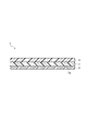
- FIG. 1 is a cross-sectional view of an optical laminate of this embodiment
- the optical laminate 1 of this embodiment is a polarizing plate in which a transparent protective film layer 3 and an antireflection layer 4 are laminated on a polarizing layer 2 .
- the optical layered body 1 is used by being attached to a display device, and the antireflection layer 4, the transparent protective film layer 3, and the polarizing layer 2 are arranged in this order from the viewing side of the display device.
- a transparent protective film may also be laminated on the surface of the polarizing layer 2 opposite to the viewing side.
- polarizing layer As the material constituting the polarizing layer 2, known materials that have been conventionally used in the manufacture of polarizing plates can be used, for example, polyvinyl alcohol resin, polyvinyl acetate resin, ethylene/vinyl acetate (EVA) resin. etc. Polyvinyl alcohol-based resins are particularly preferred. Alternatively, a uniaxially stretched film may be dyed with iodine or a dichroic dye and then treated with boric acid.
- the thickness of the polarizing layer 2 is preferably 5 ⁇ m to 20 ⁇ m, more preferably 3 ⁇ m to 15 ⁇ m, even more preferably 2 ⁇ m to 10 ⁇ m.
- the transparent protective film layer 3 functions as a protective film layer for protecting the polarizing layer 2 . Therefore, it is transparent to visible light (for example, visible light transmittance is 80% or more).
- the material constituting the transparent protective film layer 3 is preferably a resin.
- a resin for example, a cellulose-based resin, typically triacetyl cellulose, or a polyolefin-based resin, typically polypropylene-based resin (" In the category of "polyolefin resin", for example, there are alicyclic polyolefin resins typified by norbornene resins), acrylic resins typified by polymethyl methacrylate resins, and polyethylene terephthalate resins. polyester-based resins, etc. Among them, acrylic resins and cellulose resins are preferable.
- the thickness of the transparent protective film layer 3 may be 5 ⁇ m to 30 ⁇ m, 10 ⁇ m to 28 ⁇ m, or 15 ⁇ m to 25 ⁇ m. In this embodiment, even with a polarizing plate having a thin transparent protective film layer 3 and an antireflection layer on the surface, the occurrence of optical unevenness can be efficiently prevented.
- the "thickness of the transparent protective film layer 3" as used herein refers to the thickness before surface roughening, which will be described later.
- the polarizing layer 2 and the transparent protective film layer 3 are directly laminated to each other.
- the term "directly laminated” includes an embodiment in which the transparent protective film layer 3 is laminated on the polarizing layer due to the self-adhesiveness of the transparent protective film layer 3, and an embodiment in which the transparent protective film layer 3 is laminated via an adhesive or pressure-sensitive adhesive.
- an adhesive layer or pressure-sensitive adhesive layer may be interposed between the polarizing layer 2 and the transparent protective film layer 3 .
- the adhesive forming the adhesive layer various adhesives conventionally used in the manufacture of polarizing plates can be used.
- acrylic resins such as acrylamide, acrylate, urethane acrylate, and epoxy acrylate
- water-based adhesives such as polyvinyl alcohol resins
- an epoxy resin containing no aromatic ring in the molecule is preferable. It may also be cured by irradiation with active energy rays (ultraviolet rays or heat rays).
- the thickness of the adhesive layer is preferably 0.01 ⁇ m to 5 ⁇ m.
- Examples of adhesives that form the adhesive layer include acrylic resins, silicone resins, polyesters, polyurethanes, and polyethers.
- a method of laminating the pressure-sensitive adhesive layer on the polarizing layer 2 or the transparent protective film layer 3 for example, a method of applying a solution containing the resin or optional additive components to the polarizing layer 2 or the transparent protective film layer 3 may be used.
- a method of forming an adhesive layer with the solution on a prepared separator and then transferring it onto the polarizing layer 2 or the transparent protective film layer 3 may also be used.
- the thickness of the adhesive layer is preferably 2 ⁇ m to 500 ⁇ m, more preferably 5 ⁇ m to 200 ⁇ m, even more preferably 10 ⁇ m to 50 ⁇ m.
- the antireflection layer is a layer for weakening the external light reflection of the optical layered body 1 for an observer of the optical layered body 1, and usually has a reflectance of 1% or less for visible light.
- Antireflection layers of such reflectivity typically consist of a high refractive index layer with a high refractive index and a low refractive index layer with a low refractive index. By adjusting the refractive index and the thickness of each layer, the reflected light from each layer can be made to weaken each other, and an excellent antireflection function can be achieved.
- the antireflection layer consisting of a high refractive index layer and a low refractive index layer is manufactured using a coating composition capable of forming each of the high refractive index layer and the low refractive index layer, as described in detail later. Then, it is preferable because the operation is extremely simple.
- a coating type composition capable of forming each of the high refractive index layer and the low refractive index layer will be given.
- Such spreadable compositions are in liquid form and contain suitable curable resins and, if necessary, additives.
- a coating type composition capable of forming a high refractive index layer includes, for example, a curable resin such as urethane acrylate, an acetophenone-based, benzophenone-based, benzyldimethylketal-based, ⁇ -hydroxyalkyl
- a curable resin such as urethane acrylate
- An initiator for photopolymerization such as phenone, ⁇ -aminoalkylphenone or thioxanthone is dissolved in a solvent such as methyl ethyl ketone or methyl isobutyl ketone.
- a leveling agent preferably a fluorine-based leveling agent
- a leveling agent may be included in the high refractive index layer-forming coating solution.
- binders such as polyethylene glycol diacrylate and pentaerythritol (tri/tetra) acrylate are used as curable resins.
- 1-Methoxy- Silica particles are dispersed in a solution dissolved in a solvent such as 2-propyl acetate or methyl isobutyl.
- a fluorine-based leveling agent may be included in the coating liquid for forming the low refractive index layer.
- the coating type composition capable of forming each of the high refractive index layer and the low refractive index layer mentioned here is only an example, and depending on the characteristics of the antireflection layer to be formed, the composition for forming the high refractive index layer It is preferable to optimize each of the coating liquid and the coating liquid for forming the low refractive index layer.
- the outermost layer of the high refractive index layer and the low refractive index layer capable of forming the antireflection layer has an appropriate surface strength, that layer also functions as a hard coat layer.
- the above-exemplified high refractive index layer-forming coating solution containing a curable resin such as urethane acrylate is also useful as a coating composition for forming a hard coat layer.
- the reflectance is the so-called visibility reflectance
- the measuring means is as follows.
- a black polyethylene terephthalate (PET) film and a transparent film provided with an antireflection layer are attached using an appropriate adhesive in the order of antireflection layer, transparent film, adhesive, and black PET film.
- PET polyethylene terephthalate
- the side of the antireflection layer which is the object to be measured, is irradiated with light having an incident angle of 5 degrees, and the reflected light reflected by the antireflection layer in the specular direction is received, and the reflectance in the wavelength range of 380 nm to 780 nm is measured. to measure.
- the luminous reflectance can be calculated by multiplying the measured value by the relative luminous efficiency value.
- a commercially available ultraviolet-visible-near-infrared spectrophotometer for example, "UV-2450” manufactured by Shimadzu Corporation
- UV-2450 ultraviolet-visible-near-infrared spectrophotometer
- the transparent protective film layer 3 of this embodiment is characterized by the arithmetic mean roughness Ra of the surface 3a on the side to be bonded to the polarizing layer 2 .
- the arithmetic mean roughness Ra before bonding to the polarizing layer 2 may be 0.01 ⁇ m to 0.1 ⁇ m, or may be 0.02 ⁇ m to 0.08 ⁇ m.
- the arithmetic mean roughness Ra of the surface 3a of the transparent protective film layer 3 after peeling the laminated transparent protective film layer 3 and the polarizing layer 2 may be 0.01 ⁇ m to 0.1 ⁇ m. , 0.02 ⁇ m to 0.095 ⁇ m.
- the peeling processing method for peeling the transparent protective film layer 3 and the polarizing layer 2 from the optical laminate 1 is as follows. That is, the polarizing layer 2 side is attached to a glass plate using an adhesive. A cutter blade is inserted between the transparent protective film layer 3 and the polarizing layer 2 to slightly lift the transparent protective film layer 3 from the polarizing layer 2, and the lifted transparent protective film layer 3 is pinched with tweezers and peeled off little by little. .
- the equipment and conditions used for measuring the arithmetic mean roughness Ra are as follows.
- Measuring device White interferometer Objective lens: 5x (magnification) Scan range: -30 ⁇ m to 10 ⁇ m Field of view size: 640 ⁇ m ⁇ 480 ⁇ m
- Measurement mode Wave mode Surface correction: Quaternary processing
- the method for manufacturing the optical layered body 1 has at least a surface roughening step and a bonding step.
- the transparent protective film layer 3 made of resin is prepared, and a solvent in which the resin is soluble is brought into contact with one surface thereof.
- the solvent include methyl ethyl ketone
- the contact method includes application using a bar coater. Wash with water after a predetermined time has passed. This surface roughening is preferably carried out until the arithmetic mean roughness Ra of the treated surface reaches 0.01 ⁇ m or more.
- a transparent protective film layer used in the production of an optical film or the like has extremely small surface irregularities, and even if the transparent protective film layer and the polarizing layer are laminated together and then the antireflection layer is laminated, the surface roughness of the present embodiment can be reduced.
- the specific arithmetic mean roughness Ra of this embodiment cannot be achieved in the transparent protective film layer.
- the arithmetic surface roughness Ra of the transparent protective film layer is preferably set within the above range by bringing the solvent and the transparent protective film layer into contact with each other because the operation is simple. If the contact time is too long, the transparent protective film layer after treatment may lose its transparency to visible light. Therefore, it is preferable to determine the optimum treatment time based on the resin contained in the transparent protective film layer to be treated and the type of solvent capable of dissolving the resin. Appropriate preliminary experiments can also be performed to determine the optimum treatment time.
- the polarizing layer 2 is prepared, and the transparent protective film layer 3 and the polarizing layer 2 are bonded together with the roughened surface 3a of the transparent protective film layer 3 facing the polarizing layer 2 side.
- the optical laminate 1 is completed by forming the antireflection layer 4 on the other surface of the transparent protective film layer 3 with a curable coating composition.
- another transparent protective film or the like may be appropriately provided on the surface of the optical layered body 1 on the polarizing layer 2 side.
- the antireflection layer applied to this embodiment is formed by first forming a high refractive index layer on a suitable transparent resin film, and then forming a low refractive index layer on the formed high refractive index layer.
- Each of the high refractive index layer and the low refractive index layer may be one layer each, and if necessary, the high refractive index layer formation and the low refractive index layer formation are alternately performed to form a It is also possible to form an antireflection layer in which multiple layers of high refractive index layers and multiple layers of low refractive index layers are alternately laminated, and use the antireflection layer. If necessary, the antireflection layer formed on the transparent resin film can be used by peeling off the transparent resin film used as the base material, or can be used with the transparent resin film as the base material still attached. can.
- a high refractive index layer is formed from a coating solution for forming a high refractive index layer containing a curable resin such as urethane acrylate, and a low refractive index layer containing a binder resin such as polyethylene glycol diacrylate or pentaerythritol (tri/tetra) acrylate is used.
- a curable resin such as urethane acrylate
- a low refractive index layer containing a binder resin such as polyethylene glycol diacrylate or pentaerythritol (tri/tetra) acrylate.
- a coating solution for forming a high refractive index layer is applied onto a triacetyl cellulose film, which is a transparent resin film, and dried at 70° C. for 1 minute to volatilize the solvent. After that, ultraviolet rays are irradiated under the condition of 100 mJ/cm 2 to form a high refractive index layer. Subsequently, a coating solution for forming a low refractive index layer is applied onto the formed high refractive index layer, and then dried at 70° C. for 1 minute to volatilize the solvent. Subsequently, ultraviolet rays are irradiated under the condition of 200 mJ/cm 2 to form a low refractive index layer.
- an antireflection layer can be formed on the triacetylcellulose film.
- a high refractive index layer is formed on the outermost surface, for example, from a high refractive index layer-forming coating liquid containing a curable resin such as urethane acrylate, this high refractive index layer also functions as a hard coat layer.
- optical unevenness is suppressed when the optical layered body 1 is observed from the antireflection layer 4 side.
- interfacial reflection occurs at the interface between the transparent protective film layer and the polarizing layer due to the difference in refractive index between the two layers.
- the reflected light due to this interface reflection is observed by a viewer together with the reflected light on the surface of the optical layered body.
- Reflected light due to interface reflection is originally weak, so if the optical layered body does not have an antireflection layer (reflectance of 1% or less), the strong reflected light on the surface of the optical layered body is mainly visible, and the reflected light due to interface reflection is Hard to see.
- the optical layered body when the optical layered body is provided with an antireflection layer, the reflected light on the surface of the optical layered body is reduced, so the reflected light due to interface reflection becomes relatively strong and easily visible. In either case, the reflected light due to interface reflection interferes with the reflected light from the surface of the optical layered body and reaches the viewer.
- the optical laminate has an antireflection layer
- the reflected light due to interface reflection becomes more visible, and the above optical unevenness is caused by the thickness unevenness of the transparent protective film layer. It was presumed that this was caused by variations in the optical path length of the interface reflection, and a difference in the interference between the light reflected by the interface reflection and the light reflected on the surface of the optical layered body according to the thickness unevenness. . This is particularly noticeable when the thickness of the transparent protective film layer is thin.
- the peeled surface 3a on the side of the transparent protective film layer 3 has an arithmetic mean roughness Ra of 0.01 ⁇ m. That's it.
- the arithmetic mean roughness Ra after peeling reflects the surface roughness of the bonding surface 3 a when the transparent protective film layer 3 is bonded to the polarizing layer 2 . Since the surface 3a of the transparent protective film layer 3 is moderately rough, the optical laminate 1 has a high ratio of transmission and scattering of light incident from the antireflection layer 4 side on the surface 3a.
- the optical laminate 1 of the present embodiment can suppress the occurrence of optical unevenness.
- Example 2 An example of actual measurement is shown.
- three types of triacetyl cellulose films having a thickness of 25 ⁇ m were prepared as transparent protective film layers. That is, three types of surfaces to be bonded to the polyvinyl alcohol film were prepared: an untreated surface (Experimental Example 1) and a surface roughened by applying methyl ethyl ketone with a bar coater (Experimental Examples 2 and 3). did. The arithmetic average roughness Ra of these three types of surfaces was measured.
- a polyvinyl alcohol film having a thickness of 8 ⁇ m was laminated as a polarizing layer to each triacetyl cellulose film, and a high refractive index layer (thickness of 5 ⁇ m) and a low refractive index layer (thickness of 0.15 ⁇ m) were used as raw materials for the antireflection layer. ) was laminated to produce an optical laminate.
- the reflectance for visible light of the antireflection layer formed by stacking such a high refractive index layer (5 ⁇ m thick) and a low refractive index layer (0.15 ⁇ m thick) is about 1% or less.
- a water-based adhesive was used to bond the polyvinyl alcohol film and the triacetyl cellulose film.
- This water-based adhesive is composed of 3 parts of carboxy group-modified polyvinyl alcohol (Kuraray Poval KL318 manufactured by Kuraray Co., Ltd.) and 1.5 parts of water-soluble polyamide epoxy resin (Sumi (converted from 30% solid content concentration of Layz Resin 650 commercial product (aqueous solution) so as to obtain the above number of parts)).
- interference unevenness optical unevenness
- the evaluation index of interference unevenness is as follows. A: Almost no interference unevenness was observed. B: Interference unevenness was slightly observed. C: Interference unevenness was conspicuous.
- the present invention can be used in the field of polarizing plates.
Landscapes
- Physics & Mathematics (AREA)
- General Physics & Mathematics (AREA)
- Optics & Photonics (AREA)
- Polarising Elements (AREA)
- Laminated Bodies (AREA)
- Surface Treatment Of Optical Elements (AREA)
Abstract
本発明の課題は、光学的ムラを抑制できる光学積層体を提供することである。 光学積層体1は、表示装置に用いられたときの視認側からの積層順として、反射率が1%以下である反射防止層4、透明保護フィルム層3及び偏光層2がこの順に積層されてなる。透明保護フィルム層3と偏光層2とは互いに直接積層されており、下記剥離加工方法により、透明保護フィルム層3と偏光層2とを剥離したとき、透明保護フィルム層3の剥離面の算術平均粗さRaが、0.01μm以上である。 <剥離加工方法> 前記偏光層側をガラス板に貼合する。前記透明保護フィルム層と、前記偏光層との間にカッター刃を入れて前記透明保護フィルム層を前記偏光層からわずかに浮上がらせ、浮き上がった前記透明保護フィルム層をピンセットで摘まんで少しずつ剥離する。
Description
本発明は、光学積層体及びその製造方法に関する。
液晶表示装置や有機エレクトロルミネッセンス表示装置(有機EL表示装置)等の表示装置に適用される偏光板は、通常、偏光フィルムの片面又は両面に透明保護フィルム(以下、場合により「保護フィルム」という。)が貼り合わせられて成っている。また、用途に応じて位相差フィルムや反射防止フィルムが更に貼り合わせられる。近年、表示装置の薄型化、軽量化に伴って偏光板の薄型化等が進み、例えば、偏光フィルムでは厚さが3μm~5μm程度の薄型偏光フィルムが開発されてきている(特許文献1参照)。更に最近では、保護フィルムの薄膜化の検討も進んできている(非特許文献1参照)。
岩上直矢ら、「超薄膜TACフィルムの開発」、KONICA MINOLTA TECHNOLOGY REPORT、VOL.11、2014年、93~96頁
反射防止フィルムは偏光板の最表面に設けられるものであり、外部光源と視認者が偏光板に対して同じ側に位置しているときに視認者に観察される表面反射光を低減することを目的としている。本発明者らの検討では、反射防止層、保護フィルム層、偏光層をこの順に備える偏光板において、保護フィルム層の厚さを例えば30μm以下にまで薄膜化したときに、当該偏光板に目視で光学的ムラが認められた。本発明は、このような光学的ムラを抑制できる光学積層体を提供することを目的とする。また、当該光学積層体の製造方法を提供することを目的とする。
一般に、保護フィルム層と偏光層との界面では、両層の屈折率の相違に起因して界面反射が生じる。この界面反射による反射光は、偏光板表面での反射光と併せて視認者に観察される。界面反射による反射光は元々弱いので、偏光板が反射防止層を備えない場合は偏光板表面での強い反射光が主に視認され、界面反射による反射光は視認されにくい。他方、偏光板が、例えば可視光に対する反射率が1%以下程度である反射防止層を備える場合は偏光板表面での反射光が防止されるため、界面反射による反射光が相対的に強くなり、視認されやすくなる。いずれの場合でも、界面反射による反射光は偏光板表面での反射光と干渉し合って視認者に届く。本発明者の検討によれば、偏光板が上記反射率の反射防止層を備える場合に界面反射による反射光が視認されやすくなること、及び、上記の光学的ムラは、保護フィルム層の厚さムラによって界面反射の光路長にばらつきが生じ、界面反射による反射光と偏光板表面での反射光との干渉に当該厚さムラに応じた差異が生じることが原因となっていることが推定された。なお、ここで「光学的ムラ」とは、偏光板表面を観察したときに複数の色で構成される縞状又は斑状の模様が認められる状態をいう。
これを解決するため、本発明は、表示装置に用いられたときの視認側からの積層順として、反射率が1%以下である反射防止層、透明保護フィルム層及び偏光層がこの順に積層されてなる光学積層体であって、透明保護フィルム層と偏光層とは互いに直接積層されており、下記剥離加工方法により、透明保護フィルム層と偏光層とを剥離したとき、透明保護フィルム層の剥離面の下記算術平均粗さRa測定で求められる算術平均粗さRaが、0.01μm以上である光学積層体を提供する。
<剥離加工方法>
偏光層側をガラス板に貼合する。透明保護フィルム層と、偏光層との間にカッター刃を入れて透明保護フィルム層を偏光層からわずかに浮上がらせ、浮き上がった透明保護フィルム層をピンセットで摘まんで少しずつ剥離する。
<算術平均粗さRa測定>
測定装置 :白色干渉計
対物レンズ :5倍(倍率)
スキャンレンジ :-30μm~10μm
視野サイズ :640μm×480μm
測定モード :Waveモード
面補正 :4次処理
<剥離加工方法>
偏光層側をガラス板に貼合する。透明保護フィルム層と、偏光層との間にカッター刃を入れて透明保護フィルム層を偏光層からわずかに浮上がらせ、浮き上がった透明保護フィルム層をピンセットで摘まんで少しずつ剥離する。
<算術平均粗さRa測定>
測定装置 :白色干渉計
対物レンズ :5倍(倍率)
スキャンレンジ :-30μm~10μm
視野サイズ :640μm×480μm
測定モード :Waveモード
面補正 :4次処理
剥離後の算術平均粗さRaは、透明保護フィルム層が偏光層と貼合されている状態であったときの貼合面の表面粗さを反映したものとなっている。透明保護フィルム層の当該面が適度に粗いので、光学積層体は、その反射防止層側から入射した光が当該面で透過散乱する割合が高くなる。入射光が透過散乱した分だけ界面反射が弱くなるので、生じる光学的ムラが抑制される。
算術平均粗さRaが0.1μm以下であってもよい。
透明保護フィルム層が、アクリル系樹脂又はセルロース系樹脂を含むものであってもよい。また、透明保護フィルム層の厚さは5μm~30μmであってもよい。
偏光層の厚さは5μm~20μmであってもよい。
また、本発明は、透明保護フィルムの片側表面の算術平均粗さRaが0.01μm以上となるように粗化する表面粗化工程と、粗化した透明保護フィルム層の表面を偏光層に向けて、透明保護フィルム層と偏光層とを互いに積層するように貼合する貼合工程と、を有する光学積層体の製造方法を提供する。
この製造方法では、透明保護フィルム層が樹脂からなるものであり、表面粗化工程では、樹脂が可溶な溶剤に透明保護フィルム層の表面を接触させることが好ましい。
本発明によれば、光学的ムラを抑制できる光学積層体を提供することができる。また、当該光学積層体の製造方法を提供することができる。
以下、本発明の好適な実施形態について詳細に説明する。
図1に示されているとおり、本実施形態の光学積層体1は、偏光層2に透明保護フィルム層3と反射防止層4とが積層されてなる偏光板である。光学積層体1は表示装置に貼合されて使用されるものであり、表示装置の視認側から反射防止層4、透明保護フィルム層3、偏光層2の順の配置とされている。なお、図示はしていないが、偏光層2の視認側とは反対側の面にも透明保護フィルムが積層されていてもよい。
(偏光層)
偏光層2を構成する材料としては、従来から偏光板の製造に使用されている公知の材料を用いることができ、例えば、ポリビニルアルコール系樹脂、ポリ酢酸ビニル樹脂、エチレン/酢酸ビニル(EVA)樹脂等が挙げられる。なかでもポリビニルアルコール系樹脂が好ましい。また、一軸延伸したフィルムにヨウ素又は二色性染料による染色を施し、ついでホウ酸処理したものであってもよい。偏光層2の厚さは、5μm~20μmであることが好ましく、3μm~15μmであることがより好ましく、2μm~10μmであることが更に好ましい。
偏光層2を構成する材料としては、従来から偏光板の製造に使用されている公知の材料を用いることができ、例えば、ポリビニルアルコール系樹脂、ポリ酢酸ビニル樹脂、エチレン/酢酸ビニル(EVA)樹脂等が挙げられる。なかでもポリビニルアルコール系樹脂が好ましい。また、一軸延伸したフィルムにヨウ素又は二色性染料による染色を施し、ついでホウ酸処理したものであってもよい。偏光層2の厚さは、5μm~20μmであることが好ましく、3μm~15μmであることがより好ましく、2μm~10μmであることが更に好ましい。
(透明保護フィルム層)
透明保護フィルム層3は、偏光層2を保護するための保護フィルム層として機能するものである。したがって、可視光に対して透明(例えば可視光透過率が80%以上)である。透明保護フィルム層3を構成する材料としては樹脂であることが好ましく、更に、樹脂としては例えば、トリアセチルセルロースを代表例とするセルロース系樹脂、ポリプロピレン系樹脂を代表例とするポリオレフィン系樹脂(「ポリオレフィン系樹脂」の範疇には、例えばノルボルネン系樹脂を代表例とする脂環式ポリオレフィン系樹脂がある)、ポリメチルメタクリレート系樹脂を代表例とするアクリル系樹脂、ポリエチレンテレフタレート系樹脂を代表例とするポリエステル系樹脂等が挙げられる。なかでも、アクリル系樹脂又はセルロース系樹脂が好ましい。
透明保護フィルム層3は、偏光層2を保護するための保護フィルム層として機能するものである。したがって、可視光に対して透明(例えば可視光透過率が80%以上)である。透明保護フィルム層3を構成する材料としては樹脂であることが好ましく、更に、樹脂としては例えば、トリアセチルセルロースを代表例とするセルロース系樹脂、ポリプロピレン系樹脂を代表例とするポリオレフィン系樹脂(「ポリオレフィン系樹脂」の範疇には、例えばノルボルネン系樹脂を代表例とする脂環式ポリオレフィン系樹脂がある)、ポリメチルメタクリレート系樹脂を代表例とするアクリル系樹脂、ポリエチレンテレフタレート系樹脂を代表例とするポリエステル系樹脂等が挙げられる。なかでも、アクリル系樹脂又はセルロース系樹脂が好ましい。
透明保護フィルム層3の厚さは、5μm~30μmであってもよく、10μm~28μmであってもよく、15μm~25μmであってもよい。本実施形態では、このように透明保護フィルム層3の厚さを薄膜化し、表面に反射防止層を有するような偏光板であっても、光学的ムラの発生を効率的に防止できる。なお、ここでいう「透明保護フィルム層3の厚さ」とは、後述する表面粗化を行う前の厚さをいう。
偏光層2と透明保護フィルム層3とは互いに直接積層されている。ここで「直接積層されている」とは、透明保護フィルム層3の自己粘着性によって偏光層に積層されている態様、及び、接着剤又は粘着剤を介して積層されている態様を含む。
(接着剤層、粘着剤層)
図1には示されていないが、偏光層2と透明保護フィルム層3との間には、接着剤層又は粘着剤層が介在していてもよい。接着剤層をなす接着剤としては、従来から偏光板の製造に使用されている各種の接着剤を使用することができる。例えば、アクリルアミド、アクリレート、ウレタンアクリレート、エポキシアクリレート等のアクリル系樹脂や、ポリビニルアルコール系樹脂の水系接着剤を使用することもできる。また、耐候性や屈折率、カチオン重合性等の観点から、分子内に芳香環を含まないエポキシ樹脂が好ましい。また、活性エネルギー線(紫外線又は熱線)の照射によって硬化するものであってもよい。接着剤層の厚さは、0.01μm~5μmであることが好ましい。
図1には示されていないが、偏光層2と透明保護フィルム層3との間には、接着剤層又は粘着剤層が介在していてもよい。接着剤層をなす接着剤としては、従来から偏光板の製造に使用されている各種の接着剤を使用することができる。例えば、アクリルアミド、アクリレート、ウレタンアクリレート、エポキシアクリレート等のアクリル系樹脂や、ポリビニルアルコール系樹脂の水系接着剤を使用することもできる。また、耐候性や屈折率、カチオン重合性等の観点から、分子内に芳香環を含まないエポキシ樹脂が好ましい。また、活性エネルギー線(紫外線又は熱線)の照射によって硬化するものであってもよい。接着剤層の厚さは、0.01μm~5μmであることが好ましい。
粘着剤層をなす粘着剤としては、アクリル系樹脂や、シリコーン系樹脂、ポリエステル、ポリウレタン、ポリエーテル等が挙げられる。偏光層2又は透明保護フィルム層3に粘着剤層を積層する方法としては、例えば、偏光層2又は透明保護フィルム層3に上記樹脂や任意の添加成分を含む溶液を塗布する方法でもよく、別途用意したセパレータ上に当該溶液で粘着剤層を形成した後に、これを偏光層2又は透明保護フィルム層3上に転写する方法でもよい。粘着剤層の厚さは、2μm~500μmであることが好ましく、5μm~200μmであることがより好ましく、10μm~50μmであることが更に好ましい。
(反射防止層)
反射防止層は、光学積層体1を観察する者にとって、光学積層体1の外光反射を弱めるための層であり、通常は、可視光に対する反射率が1%以下となる。このような反射率の反射防止層は典型的には、高い屈折率を有する高屈折率層と、低い屈折率を有する低屈折率層とからなる。これらの屈折率と各層の厚さを調整することで各層からの反射光が互いに弱め合うようにすることができ、優れた反射防止機能が奏される。
反射防止層は、光学積層体1を観察する者にとって、光学積層体1の外光反射を弱めるための層であり、通常は、可視光に対する反射率が1%以下となる。このような反射率の反射防止層は典型的には、高い屈折率を有する高屈折率層と、低い屈折率を有する低屈折率層とからなる。これらの屈折率と各層の厚さを調整することで各層からの反射光が互いに弱め合うようにすることができ、優れた反射防止機能が奏される。
高屈折率層と低屈折率層とからなる反射防止層は、後に詳細を述べるとおり、高屈折率層及び低屈折率層のそれぞれを形成し得る塗布型組成物を用いて反射防止層を製造すると、操作が極めて簡便であるため好ましい。ここで、高屈折率層及び低屈折率層のそれぞれを形成し得る塗布型組成物の一例を挙げておく。かかる塗布型組成物は液状のものであり、適切な硬化性樹脂と、必要に応じて添加剤とを含む。高屈折率層を形成し得る塗布型組成物(高屈折率層形成用塗布液)は例えば、ウレタンアクリレートのような硬化性樹脂と、アセトフェノン系、ベンゾフェノン系、ベンジルジメチルケタール系、α-ヒドロキシアルキルフェノン系、α-アミノアルキルフェノン系やチオキサントン系といった光重合のための開始剤(光重合開始剤)とを、メチルエチルケトンやメチルイソブチルケトンといった溶剤に溶解してなる。塗布性をより良好とするために、レベリング剤、好ましくはフッ素系レベリング剤を高屈折率層形成用塗布液に含ませてもよい。また、低屈折率層を形成し得る塗布型組成物(低屈折率層形成用塗布液)としては、硬化性樹脂として、ポリエチレングリコールジアクリレートやペンタエリストール(トリ/テトラ)アクリレートのようなバインダー樹脂に、アセトフェノン系、ベンゾフェノン系、ベンジルジメチルケタール系、α-ヒドロキシアルキルフェノン系、α-アミノアルキルフェノン系やチオキサントン系といった光重合のための開始剤(光重合開始剤)を、1-メトキシ-2-プロピルアセテートやメチルイソブチルといった溶剤に溶解してなる溶液にシリカ粒子を分散させてなる。塗布性をより良好とするために、フッ素系レベリング剤を低屈折率層形成用塗布液に含ませてもよい。なお、ここで挙げた高屈折率層及び低屈折率層のそれぞれを形成し得る塗布型組成物はあくまで一例であり、形成しようとする反射防止層の特性に応じて、高屈折率層形成用塗布液及び低屈折率層形成用塗布液をそれぞれ最適化することが好ましい。
なお、反射防止層を形成し得る高屈折率層及び低屈折率層のうち、最表面に来るものが適度な表面強度を有するとき、その層はハードコート層としても機能する。上記に例示した、ウレタンアクリレートのような硬化性樹脂を含む高屈折率層形成用塗布液は、ハードコート層形成用の塗布型組成物としても有用である。
反射防止層の反射率に関し、反射率はいわゆる視感度反射率であり、その測定手段は、以下のとおりである。黒色のポリエチレンテレフタレート(PET)フィルムと、反射防止層を付与した透明フィルムとを、適当な粘着剤を用いて反射防止層、透明フィルム、粘着剤、黒色のPETフィルムの順となるように貼り付ける。続いて、被測定物である反射防止層側に入射角度5度の光を照射し、反射防止層で反射された正反射方向の反射光を受光して、380nm~780nmの波長範囲の反射率を測定する。最後に、測定値に比視感度値を乗じて視感度反射率を算出できる。測定のための装置は市販の紫外可視近赤外分光光度計(例えば、島津製作所製「UV-2450」)が使用できる。
(算術平均粗さRa)
本実施形態の透明保護フィルム層3は、偏光層2と貼合する側の面3aの算術平均粗さRaに特徴がある。偏光層2に貼合する前の算術平均粗さRaは、0.01μm~0.1μmであってもよく、0.02μm~0.08μmであってもよい。また、貼合された透明保護フィルム層3と偏光層2とを剥離した後の透明保護フィルム層3の当該面3aの算術平均粗さRaは、0.01μm~0.1μmであってもよく、0.02μm~0.095μmであってもよい。
本実施形態の透明保護フィルム層3は、偏光層2と貼合する側の面3aの算術平均粗さRaに特徴がある。偏光層2に貼合する前の算術平均粗さRaは、0.01μm~0.1μmであってもよく、0.02μm~0.08μmであってもよい。また、貼合された透明保護フィルム層3と偏光層2とを剥離した後の透明保護フィルム層3の当該面3aの算術平均粗さRaは、0.01μm~0.1μmであってもよく、0.02μm~0.095μmであってもよい。
剥離後の算術平均粗さRaを測定するに際し、光学積層体1から透明保護フィルム層3と偏光層2とを剥離するための剥離加工方法は以下のとおりとする。すなわち、偏光層2側をガラス板に粘着剤を用いて貼合する。透明保護フィルム層3と偏光層2との間にカッター刃を入れて透明保護フィルム層3を偏光層2からわずかに浮上がらせ、浮き上がった透明保護フィルム層3をピンセットで摘まんで少しずつ剥離する。
算術平均粗さRaの測定に用いる装置及び条件は、以下のとおりとする。
測定装置 :白色干渉計
対物レンズ :5倍(倍率)
スキャンレンジ :-30μm~10μm
視野サイズ :640μm×480μm
測定モード :Waveモード
面補正 :4次処理
測定装置 :白色干渉計
対物レンズ :5倍(倍率)
スキャンレンジ :-30μm~10μm
視野サイズ :640μm×480μm
測定モード :Waveモード
面補正 :4次処理
(光学積層体の製造方法)
光学積層体1の製造方法は、少なくとも表面粗化工程と貼合工程とを有する。表面粗化工程では、樹脂からなる透明保護フィルム層3を用意し、その片面表面に対して、当該樹脂が可溶な溶剤を接触させる。溶剤としては例えばメチルエチルケトンが挙げられ、接触方法としてはバーコーターによる塗布が挙げられる。所定時間経過後に水洗いする。この表面粗化は、処理面の算術平均粗さRaが0.01μm以上となるまで行うことが好ましい。
光学積層体1の製造方法は、少なくとも表面粗化工程と貼合工程とを有する。表面粗化工程では、樹脂からなる透明保護フィルム層3を用意し、その片面表面に対して、当該樹脂が可溶な溶剤を接触させる。溶剤としては例えばメチルエチルケトンが挙げられ、接触方法としてはバーコーターによる塗布が挙げられる。所定時間経過後に水洗いする。この表面粗化は、処理面の算術平均粗さRaが0.01μm以上となるまで行うことが好ましい。
例えば、光学フィルム等の製造で用いられる透明保護フィルム層は、その表面凹凸が極めて小さく、かかる透明保護フィルム層と偏光層とを貼り合わせてから反射防止層を貼り合わせても、本実施形態の透明保護フィルム層において、本実施形態の特定の算術平均粗さRaを達成することはできない。本実施形態の表面粗化工程によって透明保護フィルム層を処理し、偏光層と貼合する側の、透明保護フィルム層の表面3aの算術平均粗さRaを特定の範囲とすることで、光学的ムラの防止が実現された。かかる効果の発現は、市販の透明保護フィルム層をそのまま貼り合わせてなる偏光板の製造からは、当業者であっても導き出せるものではなく、本発明者の独自の知見に基づくものである。
表面粗化工程は、溶剤と透明保護フィルム層とを接触させて、当該透明保護フィルム層の算術表面粗さRaを上記の範囲とすることが、操作が簡便で好ましいが、溶剤と透明保護フィルムとの接触時間があまり長くなると、処理後の透明保護フィルム層の可視光に対する透明性が損なわれることがある。そのため、処理する透明保護フィルム層に含まれる樹脂と、当該樹脂を溶解し得る溶媒種とから、最適な処理時間を求めることが好ましい。最適な処理時間を求めるために、適当な予備実験を行うこともできる。
次に貼合工程として、偏光層2を用意し、粗化した透明保護フィルム層3の表面3aを偏光層2側に向けて、透明保護フィルム層3と偏光層2とを互いに貼合する。
最後に、透明保護フィルム層3の他方の面上に反射防止層4を硬化性塗布型組成物により形成することで、光学積層体1が完成する。なお、光学積層体1の偏光層2側の面には、他の透明保護フィルム等を適宜設けてもよい。
ここで、上記した高屈折率層形成用塗布液及び低屈折率層形成用塗布液のそれぞれを用いて、高屈折率層や低屈折率層を形成する、具体的な手段を記載しておく。本実施形態に適用する反射防止層は、適当な透明樹脂フィルムに上に、まずは、高屈折率層を形成し、この形成した高屈折率層上に、低屈折率層を形成する。高屈折率層及び低屈折率層のそれぞれは1層ずつであってもよく、必要に応じて、高屈折率層形成と、低屈折率層形成とを交互に行って、透明樹脂フィルム上に高屈折率層の複数層と低屈折率層の複数層とが交互に積層されている反射防止層を形成し、その反射防止層を用いることもできる。透明樹脂フィルム上に形成した反射防止層は、必要に応じて、基材として用いた透明樹脂フィルムを剥離して用いることもできるし、基材である透明樹脂フィルムが付いたまま、用いることもできる。
上記のウレタンアクリレートのような硬化性樹脂を含む高屈折率層形成用塗布液から高屈折率層形成と、ポリエチレングリコールジアクリレートやペンタエリストール(トリ/テトラ)アクリレートのようなバインダー樹脂を含む低屈折率層形成用塗布液から低屈折率層形成とを含む反射防止層の形成について、簡単に示すと以下のとおりである。
透明樹脂フィルムであるトリアセチルセルロースフィルム上に、高屈折率層形成用塗布液を塗布し、70℃条件下で1分間乾燥し溶剤を揮発させる。その後、紫外線を100mJ/cm2の条件で照射して、高屈折率層を形成する。続いて、この形成した高屈折率層の上に、低屈折率層形成用塗布液を塗布し、その後70℃条件下で1分間乾燥し溶剤を揮発させる。続いて、紫外線を200mJ/cm2の条件で照射して、低屈折率層を形成する。このような一連の操作で、トリアセチルセルロースフィルム上に反射防止層を形成できる。ここで、最表面に例えば、ウレタンアクリレートのような硬化性樹脂を含む高屈折率層形成用塗布液から高屈折率層を形成すれば、この高屈折率層はハードコート層としても機能する。
(効果)
本実施形態の光学積層体1によれば、反射防止層4側から光学積層体1を観察したときの光学的ムラが抑制される。一般に、透明保護フィルム層と偏光層との界面では、両層の屈折率の相違に起因して界面反射が生じる。この界面反射による反射光は、光学積層体表面での反射光と併せて視認者に観察される。界面反射による反射光は元々弱いので、光学積層体が反射防止層(反射率1%以下)を備えない場合は光学積層体表面での強い反射光が主に視認され、界面反射による反射光は視認されにくい。他方、光学積層体が反射防止層を備える場合は光学積層体表面での反射光が低減されるため、界面反射による反射光が相対的に強くなり、視認されやすくなる。いずれの場合でも、界面反射による反射光は光学積層体表面での反射光と干渉し合って視認者に届く。
本実施形態の光学積層体1によれば、反射防止層4側から光学積層体1を観察したときの光学的ムラが抑制される。一般に、透明保護フィルム層と偏光層との界面では、両層の屈折率の相違に起因して界面反射が生じる。この界面反射による反射光は、光学積層体表面での反射光と併せて視認者に観察される。界面反射による反射光は元々弱いので、光学積層体が反射防止層(反射率1%以下)を備えない場合は光学積層体表面での強い反射光が主に視認され、界面反射による反射光は視認されにくい。他方、光学積層体が反射防止層を備える場合は光学積層体表面での反射光が低減されるため、界面反射による反射光が相対的に強くなり、視認されやすくなる。いずれの場合でも、界面反射による反射光は光学積層体表面での反射光と干渉し合って視認者に届く。
本発明者の検討によれば、光学積層体が反射防止層を備える場合に界面反射による反射光が視認されやすくなること、及び、上記の光学的ムラは、透明保護フィルム層の厚さムラによって界面反射の光路長にばらつきが生じ、界面反射による反射光と光学積層体表面での反射光との干渉に当該厚さムラに応じた差異が生じることが原因となっていることが推定された。透明保護フィルム層の厚さが薄い場合には特にそのことが顕著である。
本実施形態の光学積層体1では、透明保護フィルム層3と偏光層2とを上記所定の条件で剥離したとき、透明保護フィルム層3側の剥離面3aの算術平均粗さRaが0.01μm以上である。この剥離後の算術平均粗さRaは、透明保護フィルム層3が偏光層2と貼合されている状態であったときの貼合面3aの表面粗さを反映したものとなっている。透明保護フィルム層3の当該面3aが適度に粗いので、光学積層体1は、その反射防止層4側から入射した光が当該面3aで透過散乱する割合が高くなる。入射光が透過散乱した分だけ界面反射が弱くなるので、生じる光学的ムラが抑制される。透明保護フィルム層3の厚さが例えば5μm~30μmのように薄い場合であっても、本実施形態の光学積層体1によれば光学的ムラの発生を抑制することができる。
(実験例)
実際の測定例を示す。はじめに、透明保護フィルム層としての厚さ25μmのトリアセチルセルロースフィルムを三種類用意した。すなわち、ポリビニルアルコールフィルムと貼り合わせる面について、未処理のもの(実験例1)と、メチルエチルケトンをバーコーターにより塗布して表面粗化したもの(実験例2、実験例3)との三種類を用意した。この三種類の当該面の算術平均粗さRaを測定した。
実際の測定例を示す。はじめに、透明保護フィルム層としての厚さ25μmのトリアセチルセルロースフィルムを三種類用意した。すなわち、ポリビニルアルコールフィルムと貼り合わせる面について、未処理のもの(実験例1)と、メチルエチルケトンをバーコーターにより塗布して表面粗化したもの(実験例2、実験例3)との三種類を用意した。この三種類の当該面の算術平均粗さRaを測定した。
各トリアセチルセルロースフィルムに対して、偏光層として厚さ8μmのポリビニルアルコールフィルムを貼合し、反射防止層の原料として高屈折率層(厚さ5μm)及び低屈折率層(厚さ0.15μm)が積層されているものを積層して光学積層体を製造した。なお、このような高屈折率層(厚さ5μm)及び低屈折率層(厚さ0.15μm)が積層されてなる反射防止層の可視光に対する反射率は1%以下程度となる。ポリビニルアルコールフィルムとトリアセチルセルロースフィルムとの貼合には水系接着剤を用いた。なお、この水系接着剤は、水100部に対して、カルボキシ基変性ポリビニルアルコール(株式会社クラレ製 クラレポバール KL318)3部と、水溶性ポリアミドエポキシ樹脂1.5部(田岡化学工業株式会社製 スミレーズレジン650市販品(水溶液)の固形分濃度30%から上記の部数となるように換算)とを添加して調製した。
その後、点灯させた蛍光灯を反射防止層側にかざして、光学積層体に映り込んだ蛍光灯の像に干渉ムラ(光学的ムラ)が生じる程度を肉眼で観察した。干渉ムラの評価指標は以下のとおりである。
A…干渉ムラがほとんど認められなかった。
B…干渉ムラが僅かに認められた。
C…干渉ムラが目立った。
A…干渉ムラがほとんど認められなかった。
B…干渉ムラが僅かに認められた。
C…干渉ムラが目立った。
その後、上述した方法でトリアセチルセルロースフィルムをポリビニルアルコールフィルムから剥離し、トリアセチルセルロースフィルムの当該面の算術平均粗さRaを測定した。各測定結果を表1に示す。これらの記載から、透明保護フィルムの表面を粗化することで光学積層体の干渉ムラを抑制できたことが分かる。

本発明は、偏光板分野で利用することができる。
1…光学積層体、2…偏光層、3…透明保護フィルム層、3a…透明保護フィルム層の表面、4…反射防止層。
Claims (7)
- 表示装置に用いられたときの視認側からの積層順として、反射率が1%以下である反射防止層、透明保護フィルム層及び偏光層がこの順に積層されてなる光学積層体であって、 前記透明保護フィルム層と前記偏光層とは互いに直接積層されており、
下記剥離加工方法により、前記透明保護フィルム層と前記偏光層とを剥離したとき、前記透明保護フィルム層の剥離面の下記算術平均粗さRa測定で求められる算術平均粗さRaが、0.01μm以上である、光学積層体。
<剥離加工方法>
前記偏光層側をガラス板に貼合する。前記透明保護フィルム層と、前記偏光層との間にカッター刃を入れて前記透明保護フィルム層を前記偏光層からわずかに浮上がらせ、浮き上がった前記透明保護フィルムをピンセットで摘まんで少しずつ剥離する。
<算術平均粗さRa測定>
測定装置 :白色干渉計
対物レンズ :5倍(倍率)
スキャンレンジ :-30μm~10μm
視野サイズ :640μm×480μm
測定モード :Waveモード
面補正 :4次処理 - 前記算術平均粗さRaが0.1μm以下である請求項1記載の光学積層体。
- 前記透明保護フィルム層が、アクリル系樹脂又はセルロース系樹脂を含むものである請求項1又は2記載の光学積層体。
- 前記透明保護フィルム層の厚さが5μm~30μmである請求項1~3のいずれか一項記載の光学積層体。
- 前記偏光層の厚さが5μm~20μmである請求項1~4のいずれか一項記載の光学積層体。
- 透明保護フィルム層の片側表面の算術平均粗さRaが0.01μm以上となるように粗化する表面粗化工程と、
粗化した前記透明保護フィルム層の表面を偏光層に向けて、前記透明保護フィルム層と前記偏光層とを互いに積層するように貼合する貼合工程と、を有する光学積層体の製造方法。 - 前記透明保護フィルム層が樹脂からなるものであり、
前記表面粗化工程では、前記樹脂が可溶な溶剤に前記透明保護フィルム層の表面を接触させる、請求項6記載の光学積層体の製造方法。
Priority Applications (2)
| Application Number | Priority Date | Filing Date | Title |
|---|---|---|---|
| KR1020237030324A KR20240000454A (ko) | 2021-04-26 | 2022-04-21 | 광학 적층체, 및 그 제조 방법 |
| CN202280029165.4A CN117177863A (zh) | 2021-04-26 | 2022-04-21 | 光学层叠体及其制造方法 |
Applications Claiming Priority (2)
| Application Number | Priority Date | Filing Date | Title |
|---|---|---|---|
| JP2021074124A JP7708578B2 (ja) | 2021-04-26 | 2021-04-26 | 光学積層体、及びその製造方法 |
| JP2021-074124 | 2021-04-26 |
Publications (1)
| Publication Number | Publication Date |
|---|---|
| WO2022230751A1 true WO2022230751A1 (ja) | 2022-11-03 |
Family
ID=83847133
Family Applications (1)
| Application Number | Title | Priority Date | Filing Date |
|---|---|---|---|
| PCT/JP2022/018390 Ceased WO2022230751A1 (ja) | 2021-04-26 | 2022-04-21 | 光学積層体、及びその製造方法 |
Country Status (4)
| Country | Link |
|---|---|
| JP (1) | JP7708578B2 (ja) |
| KR (1) | KR20240000454A (ja) |
| CN (1) | CN117177863A (ja) |
| WO (1) | WO2022230751A1 (ja) |
Citations (5)
| Publication number | Priority date | Publication date | Assignee | Title |
|---|---|---|---|---|
| JP2010286827A (ja) * | 2009-05-14 | 2010-12-24 | Jiroo Corporate Plan:Kk | 偏光子保護フィルム、偏光板及び液晶表示素子 |
| JP2015110757A (ja) * | 2013-10-31 | 2015-06-18 | 住友化学株式会社 | (メタ)アクリル系樹脂組成物及びそれを用いた(メタ)アクリル系樹脂フィルム |
| JP2017068223A (ja) * | 2015-10-02 | 2017-04-06 | 住友化学株式会社 | 偏光板用保護フィルム |
| WO2019139095A1 (ja) * | 2018-01-11 | 2019-07-18 | 東洋紡株式会社 | 積層フィルム及びそれを用いた偏光板並びに画像表示装置 |
| JP2021047359A (ja) * | 2019-09-20 | 2021-03-25 | 住友化学株式会社 | 偏光板及び画像表示装置 |
Family Cites Families (1)
| Publication number | Priority date | Publication date | Assignee | Title |
|---|---|---|---|---|
| JP2014115673A (ja) | 2010-09-03 | 2014-06-26 | Nitto Denko Corp | 積層体 |
-
2021
- 2021-04-26 JP JP2021074124A patent/JP7708578B2/ja active Active
-
2022
- 2022-04-21 CN CN202280029165.4A patent/CN117177863A/zh active Pending
- 2022-04-21 WO PCT/JP2022/018390 patent/WO2022230751A1/ja not_active Ceased
- 2022-04-21 KR KR1020237030324A patent/KR20240000454A/ko active Pending
Patent Citations (5)
| Publication number | Priority date | Publication date | Assignee | Title |
|---|---|---|---|---|
| JP2010286827A (ja) * | 2009-05-14 | 2010-12-24 | Jiroo Corporate Plan:Kk | 偏光子保護フィルム、偏光板及び液晶表示素子 |
| JP2015110757A (ja) * | 2013-10-31 | 2015-06-18 | 住友化学株式会社 | (メタ)アクリル系樹脂組成物及びそれを用いた(メタ)アクリル系樹脂フィルム |
| JP2017068223A (ja) * | 2015-10-02 | 2017-04-06 | 住友化学株式会社 | 偏光板用保護フィルム |
| WO2019139095A1 (ja) * | 2018-01-11 | 2019-07-18 | 東洋紡株式会社 | 積層フィルム及びそれを用いた偏光板並びに画像表示装置 |
| JP2021047359A (ja) * | 2019-09-20 | 2021-03-25 | 住友化学株式会社 | 偏光板及び画像表示装置 |
Also Published As
| Publication number | Publication date |
|---|---|
| TW202248686A (zh) | 2022-12-16 |
| JP2022168574A (ja) | 2022-11-08 |
| CN117177863A (zh) | 2023-12-05 |
| JP7708578B2 (ja) | 2025-07-15 |
| KR20240000454A (ko) | 2024-01-02 |
Similar Documents
| Publication | Publication Date | Title |
|---|---|---|
| JP7778080B2 (ja) | ヘッドマウントディスプレイ用光学系の製造方法 | |
| KR102242306B1 (ko) | 편광판의 제조 방법 | |
| JP5871408B1 (ja) | 偏光板および光学積層体 | |
| KR20170012322A (ko) | 광학 적층체 및 화상 표시 장치 | |
| WO2019088192A1 (ja) | 反射防止層付偏光板およびその製造方法 | |
| JP5871407B1 (ja) | 偏光板 | |
| KR102525401B1 (ko) | 편광판, 액정 패널 및 액정 표시 장치 | |
| JP2013200445A (ja) | 円偏光板 | |
| KR102535072B1 (ko) | 편광판 및 액정 표시 장치 | |
| JP2009175685A (ja) | 偏光板およびそれを用いた液晶表示装置 | |
| JP2008197310A (ja) | 薄型偏光板、複合偏光板、画像表示装置、及び複合偏光板の製造方法 | |
| WO2019116969A1 (ja) | 硬化性組成物、光学積層体及び画像表示装置 | |
| JP7564170B2 (ja) | 光学シート | |
| WO2023054595A1 (ja) | 光学積層体及び画像表示装置 | |
| TWI746623B (zh) | 偏光消除元件 | |
| JP2025120279A (ja) | ハードコート層付偏光板および該ハードコート層付偏光板を含む画像表示装置 | |
| JP7708578B2 (ja) | 光学積層体、及びその製造方法 | |
| JP6782676B2 (ja) | 偏光板、及び液晶表示装置 | |
| KR102601679B1 (ko) | 적층체, 이를 포함하는 편광판 및 이의 제조방법 | |
| TW201022739A (en) | Polarizing plate, liquid crystal cell and liquid crystal display | |
| WO2023054463A1 (ja) | 積層フィルム、光学積層体及び画像表示装置 | |
| KR102522332B1 (ko) | 접착제 조성물 및 편광판 | |
| JP7659482B2 (ja) | 偏光板の製造方法 | |
| CN111788502A (zh) | 偏振片及其制造方法 | |
| JP2023053913A (ja) | 光学積層体及び画像表示装置 |
Legal Events
| Date | Code | Title | Description |
|---|---|---|---|
| 121 | Ep: the epo has been informed by wipo that ep was designated in this application |
Ref document number: 22795664 Country of ref document: EP Kind code of ref document: A1 |
|
| NENP | Non-entry into the national phase |
Ref country code: DE |
|
| 122 | Ep: pct application non-entry in european phase |
Ref document number: 22795664 Country of ref document: EP Kind code of ref document: A1 |