WO2022225030A1 - 超音波受信器及び超音波観測装置 - Google Patents
超音波受信器及び超音波観測装置 Download PDFInfo
- Publication number
- WO2022225030A1 WO2022225030A1 PCT/JP2022/018488 JP2022018488W WO2022225030A1 WO 2022225030 A1 WO2022225030 A1 WO 2022225030A1 JP 2022018488 W JP2022018488 W JP 2022018488W WO 2022225030 A1 WO2022225030 A1 WO 2022225030A1
- Authority
- WO
- WIPO (PCT)
- Prior art keywords
- piezoelectric element
- stealth
- amplifier
- wave
- ultrasonic
- Prior art date
- Legal status (The legal status is an assumption and is not a legal conclusion. Google has not performed a legal analysis and makes no representation as to the accuracy of the status listed.)
- Ceased
Links
Images















Classifications
-
- H—ELECTRICITY
- H04—ELECTRIC COMMUNICATION TECHNIQUE
- H04R—LOUDSPEAKERS, MICROPHONES, GRAMOPHONE PICK-UPS OR LIKE ACOUSTIC ELECTROMECHANICAL TRANSDUCERS; ELECTRIC HEARING AIDS; PUBLIC ADDRESS SYSTEMS
- H04R17/00—Piezoelectric transducers; Electrostrictive transducers
-
- G—PHYSICS
- G01—MEASURING; TESTING
- G01V—GEOPHYSICS; GRAVITATIONAL MEASUREMENTS; DETECTING MASSES OR OBJECTS; TAGS
- G01V1/00—Seismology; Seismic or acoustic prospecting or detecting
- G01V1/16—Receiving elements for seismic signals; Arrangements or adaptations of receiving elements
- G01V1/18—Receiving elements, e.g. seismometer, geophone or torque detectors, for localised single point measurements
- G01V1/186—Hydrophones
-
- G—PHYSICS
- G01—MEASURING; TESTING
- G01S—RADIO DIRECTION-FINDING; RADIO NAVIGATION; DETERMINING DISTANCE OR VELOCITY BY USE OF RADIO WAVES; LOCATING OR PRESENCE-DETECTING BY USE OF THE REFLECTION OR RERADIATION OF RADIO WAVES; ANALOGOUS ARRANGEMENTS USING OTHER WAVES
- G01S7/00—Details of systems according to groups G01S13/00, G01S15/00, G01S17/00
- G01S7/52—Details of systems according to groups G01S13/00, G01S15/00, G01S17/00 of systems according to group G01S15/00
- G01S7/52017—Details of systems according to groups G01S13/00, G01S15/00, G01S17/00 of systems according to group G01S15/00 particularly adapted to short-range imaging
- G01S7/52079—Constructional features
-
- G—PHYSICS
- G01—MEASURING; TESTING
- G01S—RADIO DIRECTION-FINDING; RADIO NAVIGATION; DETERMINING DISTANCE OR VELOCITY BY USE OF RADIO WAVES; LOCATING OR PRESENCE-DETECTING BY USE OF THE REFLECTION OR RERADIATION OF RADIO WAVES; ANALOGOUS ARRANGEMENTS USING OTHER WAVES
- G01S7/00—Details of systems according to groups G01S13/00, G01S15/00, G01S17/00
- G01S7/52—Details of systems according to groups G01S13/00, G01S15/00, G01S17/00 of systems according to group G01S15/00
- G01S7/521—Constructional features
-
- A—HUMAN NECESSITIES
- A61—MEDICAL OR VETERINARY SCIENCE; HYGIENE
- A61B—DIAGNOSIS; SURGERY; IDENTIFICATION
- A61B8/00—Diagnosis using ultrasonic, sonic or infrasonic waves
- A61B8/44—Constructional features of the ultrasonic, sonic or infrasonic diagnostic device
- A61B8/4444—Constructional features of the ultrasonic, sonic or infrasonic diagnostic device related to the probe
-
- G—PHYSICS
- G10—MUSICAL INSTRUMENTS; ACOUSTICS
- G10K—SOUND-PRODUCING DEVICES; METHODS OR DEVICES FOR PROTECTING AGAINST, OR FOR DAMPING, NOISE OR OTHER ACOUSTIC WAVES IN GENERAL; ACOUSTICS NOT OTHERWISE PROVIDED FOR
- G10K11/00—Methods or devices for transmitting, conducting or directing sound in general; Methods or devices for protecting against, or for damping, noise or other acoustic waves in general
- G10K11/18—Methods or devices for transmitting, conducting or directing sound
Definitions
- the present invention relates to an ultrasonic receiver such as a hydrophone (underwater microphone) used for measuring a sound field, and in particular to an ultrasonic receiver with a built-in amplifier, which is applicable to medical ultrasonic diagnostic equipment and the like.
- the present invention relates to an ultrasonic observation device using a sound wave receiver.
- the signal source capacitance of the piezoelectric element is about 0.1 pF, whereas the wiring capacitance from the piezoelectric element to the amplifier is about 10 pF. extremely low.
- placing an integrated circuit chip as an amplifier in the vicinity of a piezoelectric element causes the tip of the ultrasonic probe to become large, which is not practical (Patent Reference 1).
- Non-Patent Document 1 In view of this point, due to the recent miniaturization of integrated circuit chips, attempts have been made to dispose the amplifier in the vicinity of the piezoelectric element (see Non-Patent Document 1). However, as a result of investigation by the present inventor, it was found that in such a case, a new problem of unwanted echo arises, in which the ultrasonic wave transmitted through the piezoelectric element is reflected by the integrated circuit chip and re-entered into the piezoelectric element.
- Non-Patent Document 1 in a hydrophone having a tip portion covered with a metal housing and a piezoelectric element having a curved surface, the influence of diffracted waves from the edge of the piezoelectric element is studied. No consideration has been given to the problem of unwanted echoes generated by the incoming reflected waves.
- the present invention has been devised in view of the problems described above, and an object of the present invention is to provide an ultrasonic receiver that has a compact structure, high sensitivity, and a high S/N ratio.
- the first aspect of the present invention includes (a) a resin horn portion having a sound field detection axis as a center axis and having a tapered tip, and (b) a tip end of the resin horn portion. and (c) the interior of the resin horn, which is located at the set shortest distance from the piezoelectric element in the area behind the projection of the outer shape of the piezoelectric element along the central axis.
- the piezoelectric element amplifies the electrical signal generated by electroacoustic conversion, and the ultrasonic wave parallel to the sound field detection axis changes the reflection characteristics of the transmitted wave transmitted through the piezoelectric element, and the reflected wave of the transmitted wave is reflected by the piezoelectric element.
- the gist of the invention is an ultrasonic receiver comprising an input connection means for connecting to the ultrasonic receiver. From the description of the background art, it may seem that the shorter the distance between the piezoelectric element and the stealth amplifier, the better. There is a theoretical optimum that should not be shorter than this. This theoretical optimum value is the minimum value (minimum value) of the curve showing the variation of the input connection parasitic capacitance of the input connection means, as illustrated in FIG. 2B.
- FIG. 1 minimum value of the curve showing the variation of the input connection parasitic capacitance of the input connection means
- the "set shortest distance” is a value determined by design as a possible value in terms of actual manufacturing technology based on the theoretical optimal value.
- a second aspect of the present invention comprises (g) a resin horn portion having a tapered tip having a sound field detection axis as a central axis, and (h) a portion of the resin horn portion exposed at the tip end and (i) the piezoelectric element is arranged at a set shortest distance from the piezoelectric element at a position deviated from a rear area in which the external shape of the piezoelectric element is projected along the central axis inside the resin horn portion, and the piezoelectric element amplifies the electrical signal generated by electroacoustic conversion, and the ultrasonic waves parallel to the sound field detection axis pass through the piezoelectric element.
- the set shortest distance between the piezoelectric element and the stealth amplifier is determined by design based on the minimum value (theoretical value) of the input connection parasitic capacitance parasitic on the input connection means. Distance.
- the input connection parasitic capacitance is given by the sum of a component that increases depending on the distance between the piezoelectric element and the stealth amplifier and a component that decreases in inverse proportion to the distance.
- the fact that the “set shortest distance” in the ultrasonic receiver according to the second aspect is also a value as close as possible to the theoretical minimum value of the curve illustrated in FIG. It is similar to the vessel.
- a third aspect of the present invention comprises (l) a main body having, on one end side, a resin horn portion with a tapered tip that has a sound field detection axis as a central axis, and (m) a portion of which is exposed at the tip.
- the piezoelectric element which is inside the resin horn part and is arranged at a set shortest distance from the piezoelectric element in the rear area where the outer shape of the piezoelectric element is projected along the central axis, and the piezoelectric element is Amplify the electric signal generated by electroacoustic conversion, and change the reflection characteristics of the transmitted wave transmitted through the piezoelectric element by the ultrasonic wave parallel to the sound field detection axis, so that the reflected wave of the transmitted wave does not enter the piezoelectric element, or (o) an input connection means for electrically connecting between the piezoelectric element and the stealth amplifier; and (p) the other side of the main body.
- the gist of the invention is an ultrasonic observation apparatus comprising: a transmission line having a connection parasitic capacitance and connected to an external terminal; and (s) an observation device connected to the transmission line.
- the set shortest distance used in the ultrasonic observation apparatus according to the third aspect is determined by design so that the input connection parasitic capacitance parasitic on the input connection means is smaller than 1/10 of the external connection parasitic capacitance. is the distance between the element and the stealth amplifier.
- the fourth aspect of the present invention includes (t) a main body having a tapered resin horn on one end side, and (u) a portion exposed at the tip. and (v) the piezoelectric element, which is inside the resin horn portion, at a position offset from the rear region where the outer shape of the piezoelectric element is projected along the central axis, at a set shortest distance from the piezoelectric element.
- the piezoelectric element amplifies the electric signal generated by electroacoustic conversion, and the reflected wave of the transmitted wave transmitted through the piezoelectric element by the ultrasonic wave parallel to the sound field detection axis is not input to the piezoelectric element, or the wavefront of the reflected wave is Electrical connection between the stealth amplifier set so that the input to the piezoelectric element is not uniform, (w) the external terminal connected to the other end of the main body, and (x) the stealth amplifier and the external terminal (y) a transmission line having an external connection parasitic capacitance that is at least 50 times greater than the signal source capacitance inherent in the piezoelectric element and connected to an external terminal; and (z) a transmission line connected to the The gist is that it is an ultrasonic observation device equipped with observation equipment.
- the set shortest distance used in the ultrasonic observation apparatus is determined by design so that the input connection parasitic capacitance parasitic on the input connection means is a value smaller than 1/10 of the external connection parasitic capacitance. is the distance between the element and the stealth amplifier.
- an ultrasonic receiver having a compact structure, high sensitivity and a high S/N ratio, and an ultrasonic observation apparatus using this ultrasonic receiver.
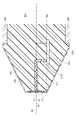
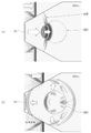
- FIG. 1 is a schematic cross-sectional view illustrating an overview of an ultrasonic receiver according to a first embodiment of the present invention
- FIG. 1B is a schematic cross-sectional view of the ultrasonic receiver according to the first embodiment viewed from a direction perpendicular to the cross-sectional view shown in FIG. 1A with respect to the sound field detection axis AX of FIG. 1A
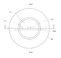
- FIG. 1 is a front view of an ultrasonic receiver according to a first embodiment
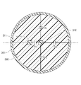
- FIG. 1B is a cross-sectional view of the ultrasonic receiver according to the first embodiment in a cross section perpendicular to the sound field detection axis AX of FIG. 1A
- FIG. 4 is a diagram for explaining the distance between the piezoelectric element and the integrated circuit chip and the input connection parasitic capacitance parasitic on the wiring connecting the piezoelectric element and the integrated circuit chip; 4 is a curve showing the variation of input connection parasitic capacitance between a piezoelectric element and an integrated circuit chip with respect to the distance between the piezoelectric element and the integrated circuit chip; 1 is a diagram showing an example of the overall structure of an ultrasonic receiver according to a first embodiment; FIG. FIG. 3B is a schematic diagram illustrating an example in which the ultrasonic receiver shown in FIG.
- 3A is connected to an external device (observation device) to configure the ultrasonic observation apparatus according to the first embodiment
- 3B is a bird's-eye view showing an enlarged tip portion X of the ultrasonic receiver according to the first embodiment shown in FIG. 3A
- FIG. Regarding the ultrasonic wave (transmitted wave) that reaches the ultrasonic receiver from the outside and has passed through the piezoelectric element, the peak of the transmitted wave at the timing when the transmitted wave reaches the integrated circuit chip 240 ns after reaching the piezoelectric element.
- 1 is a conceptual schematic diagram for explaining a wavefront of .
- FIG. 5 is a diagram for explaining that the position and shape of the wavefront used in explaining the propagation and reflection of ultrasonic waves inside the ultrasonic receiver in FIG. be.
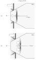
- FIG. 7(a) is before the ultrasonic wave from the outside reaches the ultrasonic receiver (-20 ns)
- Fig. 7(b) is the moment when the ultrasonic wave from the outside reaches the piezoelectric element of the ultrasonic receiver (0 ns)
- FIG. 7(c) is a diagram showing the wave front of the wave crest of the transmitted wave at the timing of 200 ns after the ultrasonic wave reaches the piezoelectric element
- FIG. 7(d) is the timing after 400 ns after the ultrasonic wave reaches the piezoelectric element, as the intensity of the sound pressure. is.
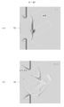
- FIG. 4 is a diagram showing the wave front of the wave crest of the reflected wave reflected by the chip as the intensity of the sound pressure.
- FIG. 10 is a diagram showing the wave front of the wave crest of the reflected wave reflected by the integrated circuit chip at the timing 400 ns after reaching , as the intensity of the pressure.
- FIG. 11(b) shows the ultrasonic wave.
- FIG. 10 is a diagram showing, as sound pressure intensity, the wave front of the wave crest of the reflected wave reflected by the integrated circuit chip at the timing 400 ns after reaching the piezoelectric element.
- FIG. 12(b) shows the ultrasonic wave.
- FIG. 10 is a diagram showing, as sound pressure intensity, the wave front of the wave crest of the reflected wave reflected by the integrated circuit chip at the timing 260 ns after reaching the piezoelectric element.
- FIG. 13(b) shows the ultrasonic wave.
- FIG. 10 is a diagram showing the wave front of the wave crest of the reflected wave reflected by the integrated circuit chip at the timing 300 ns after reaching the piezoelectric element, as the intensity of the sound pressure.
- FIG. 13(b) shows the ultrasonic wave.
- FIG. 10 is a diagram showing the wave front of the wave crest of
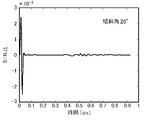
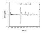
- FIG. 10 is a waveform diagram showing the influence of reflected waves on the S/N ratio when the chip main surface tilt angle
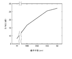
- FIG. 4 is a diagram showing the relationship between the minimum angle at which the wavefront of ultrasonic waves intersects with the main surface of the integrated circuit chip and the S/N ratio;
- FIG. 5 is a schematic cross-sectional view illustrating an outline of an ultrasonic receiver according to a second embodiment of the present invention
- 17B is a schematic cross-sectional view of the ultrasonic receiver according to the second embodiment viewed from a direction perpendicular to the cross-sectional view shown in FIG. 17A with respect to the sound field detection axis AX of FIG. 17A
- FIG. 18(b) is a diagram showing the wave front of the wave crest of the reflected wave reflected by the integrated circuit chip at the timing 300 ns after the ultrasonic wave reaches the piezoelectric element as the intensity of the sound pressure.
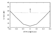
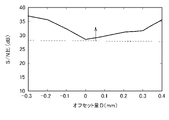
- FIG. 10 is a diagram showing the relationship between the offset amount D of the integrated circuit chip and the S/N ratio in the ultrasonic receiver according to the second embodiment;
- FIG. 10 is a diagram showing the relationship between the offset amount D of the integrated circuit chip and the S/N ratio in the ultrasonic receiver according to the second embodiment;
- FIG. 10 is a diagram showing the relationship between the offset amount D of the integrated circuit chip and the S/N ratio
- FIG. 11 is a schematic cross-sectional view illustrating an outline of an ultrasonic receiver according to a first modification of the second embodiment of the present invention
- FIG. 21B is a schematic cross-sectional view of the ultrasonic receiver according to the first modification of the second embodiment viewed from a direction orthogonal to the cross-sectional view shown in FIG. 21A with respect to the sound field detection axis AX of FIG. 21A;
- the chip main surface inclination angle ⁇ of the integrated circuit chip having a vertical end surface is 45°, the transmitted wave is transmitted before the edge of the integrated circuit chip.
- FIG. 10 is a diagram showing the wave front of the crest of the transmitted wave at the timing of the arrival moment (160 ns) as the intensity of the sound pressure.
- the chip main surface tilt angle ⁇ of the integrated circuit chip having the vertical end face is 45°, the transmitted wave proceeds from the end of the integrated circuit chip toward the center, following the state shown in FIG. 22A.
- FIG. 4 is a diagram showing, as sound pressure intensities, a wave front of a transmitted wave at a timing (220 ns) and a wave front of a reflected wave reflected at an edge of an integrated circuit chip.
- the chip main surface tilt angle ⁇ of the integrated circuit chip having vertical end faces is 45°, the transmitted wave travels from the central portion of the integrated circuit chip toward the opposite end portion following the state shown in FIG.
- each wave front such as the wave front of the wave front of the transmitted wave at the timing (280 ns), the reflected wave reflected by the main surface of the integrated circuit chip, and the transmitted wave transmitted through the integrated circuit chip is shown as the intensity of the sound pressure. be.
- FIG. 2 is a diagram showing wavefronts of wavefronts of a transmitted wave, a reflected wave reflected by the main surface of an integrated circuit chip, a transmitted wave transmitted through the integrated circuit chip, etc.
- FIG. 10 is a diagram showing the wavefronts of the wavefronts of the transmitted wave at the timing (400 ns), the reflected wave reflected by the main surface of the integrated circuit chip, the transmitted wave transmitted through the integrated circuit chip, etc. as the intensity of the sound pressure.
- FIG. 10 is a diagram showing the wavefronts of the wavefronts of the transmitted wave at the timing (400 ns), the reflected wave reflected by the main surface of the integrated circuit chip, the transmitted wave transmitted through the integrated circuit chip, etc. as the intensity of the sound pressure.
- 23(b) shows the wave front of the wave crest of the transmitted wave at the moment (200 ns) when the transmitted wave reaches the vicinity of the boundary between the main surface and the inclined end face of the integrated circuit chip. Following the state, the boundary between the main surface and the inclined end surface of the integrated circuit chip and the wave front of the wave crest of the reflected wave reflected at the main surface at the timing 380 ns after the ultrasonic wave reached the piezoelectric element are shown as the intensity of the sound pressure. It is a diagram.
- FIG. 17B is a schematic diagram illustrating the structure of an ultrasonic receiver according to a second modification of the second embodiment of the present invention, in which the chip main surface inclination angle ⁇ is increased from the chip main surface inclination angle ⁇ shown in FIG. 17B; It is a sectional view.
- FIG. 17B is a schematic diagram illustrating the structure of an ultrasonic receiver according to a second modification of the second embodiment of the present invention, in which the chip main surface inclination angle ⁇ is increased from the chip main surface inclination angle
- FIG. 27(a) shows an example using a normal integrated circuit chip having a vertical end surface.
- FIG. 27(b) shows the wave front of the wave crest of the transmitted wave at the moment (160 ns) when it reaches the back side edge of the integrated circuit chip at the timing of 240 ns after reaching the piezoelectric element, following the state shown in FIG.
- FIG. 27(c) shows the wavefront of the wavefront of the reflected wave reflected by the back surface of the chip, which is the same as that of FIG. 27(d) shows the wave front of the wave crest of the transmitted wave at the moment (180 ns) when the transmitted wave reaches the end of the main surface of the integrated circuit chip in the case of 0.4 mm.
- FIG. 2 is a diagram showing wavefronts as intensities of sound pressure, respectively;
- the offset amount is changed with respect to the time change of the intensity of the reflected wave. It is a waveform diagram showing.
- FIG. 11 is a schematic cross-sectional view illustrating an outline of an ultrasonic receiver according to a comparative example of the third embodiment of the present invention
- FIG. 30B is a schematic cross-sectional view of the ultrasonic receiver according to the comparative example of the third embodiment viewed from a direction perpendicular to the cross-sectional view shown in FIG. 30A with respect to the sound field detection axis AX of FIG. 30A
- FIG. 11 is a diagram for explaining reflection of ultrasonic waves from output lines existing in the main body of the ultrasonic receiver in the ultrasonic receiver according to the comparative example of the third embodiment
- FIG. 30B is a schematic cross-sectional view of the ultrasonic receiver according to the comparative example of the third embodiment viewed from a direction perpendicular to the cross-sectional view shown in FIG. 30A with respect to the sound field detection axis AX of FIG. 30A
- FIG. 11 is a diagram for explaining reflection of ultrasonic waves from output lines existing in the main body of the ultra
- FIG. 31B is a waveform diagram showing the intensity of unnecessary echo reflected by the output line, which is a problem in the structure of the comparative example of the third embodiment shown in FIG. 31A;
- FIG. 30B is a diagram for explaining the comparative example shown in FIG. 30B, and is a schematic cross-sectional view of the ultrasonic receiver according to the third embodiment viewed from a direction orthogonal to the cross-sectional view shown in FIG. 30A.
- the ultrasonic receiver according to the third embodiment even if there is an output line in the main body of the ultrasonic receiver, by arranging the screen member, it is possible to suppress the reflection of the ultrasonic wave from the output line. It is a figure explaining.
- FIG. 10 is a waveform diagram showing that the intensity of unnecessary echoes due to reflected waves reflected from the output line disappears in the ultrasonic receiver according to the third embodiment.
- FIG. 4 is a diagram showing a wave front of a wave crest
- FIG. 4 is a diagram showing a wave front of a wave crest
- FIG. 10 is a diagram showing the relationship between the thickness of an integrated circuit chip and the S/N ratio in the ultrasonic receiver according to the fourth embodiment
- 11 is a schematic cross-sectional view illustrating an outline of an ultrasonic receiver according to a fifth embodiment of the present invention
- FIG. 12 is a waveform diagram showing the influence of the reflected wave from the integrated circuit chip on the S/N ratio as the intensity of the reflected wave when the integrated circuit chip is a polyimide substrate in the ultrasonic receiver according to the fifth embodiment; .
- FIG. 5 is a schematic cross-sectional view illustrating an outline of an ultrasonic receiver according to another embodiment of the present invention;
- FIG. 10 is a diagram showing a wavefront of a transmitted wave directed toward a cylindrical tip and a wavefront of a reflected wave reflected by the cylindrical tip, in an ultrasonic receiver according to another embodiment;
- FIG. 10 is a waveform diagram showing the influence of the reflected wave from the cylindrical chip on the S/N ratio as the intensity of the reflected wave in an ultrasonic receiver according to another embodiment.
- FIG. 10 is a diagram showing the relationship between the radius of curvature of a spherical surface and the influence of reflected waves from the spherical surface on the S/N ratio in an ultrasonic receiver according to another embodiment having a spherical integrated circuit chip.
- first to fifth embodiments shown below exemplify a method for embodying the technical idea of the present invention, an apparatus used in the method, etc.
- the technical idea of the present invention is The material, shape, structure, arrangement, etc. of the components, the procedure of the method, etc. are not specified as follows.
- the technical idea of the present invention is not limited to the contents described in the first to fifth embodiments, and various modifications can be made within the technical scope defined by the claims described in the claims. can be done. Further, the definitions of directions such as up and down in the following description are merely definitions for convenience of description, and do not limit the technical idea of the present invention.
- the ultrasonic receiver according to the first embodiment of the present invention includes a tapered horn-shaped resin horn (300, 301) made of a polymer material, and the resin horn.
- a piezoelectric element (piezoelectric electroacoustic transducer) 10 provided at the tapered tip of the horn portion (300, 301), and the shortest distance set to the piezoelectric element 10 inside the resin horn portion (300, 301).
- the stealth amplifier 200a is arranged in the vicinity of the piezoelectric element 10 at a distance equivalent to dopt , and the input connecting means (resin signal wiring) 312 and the resin grounding wiring 311 for electrically connecting the piezoelectric element 10 and the stealth amplifier 200a.
- the set shortest distance d opt designed in consideration of process technology limitations is defined so as to approach the theoretical value defined by Equation (3).
- the stealth amplifier 200a defines the distance between the stealth amplifier 200a and the piezoelectric element 10 with this set shortest distance dopt , so that the input connection parasitic capacitance of the input connection means connecting the piezoelectric element 10 and the stealth amplifier 200a is reduced.
- C_stray can be made as small as possible.
- the resin horn portion (300, 301) consists of an insulating resin 300 forming a main portion and a thin conductive resin layer 301 serving as a skin portion surrounding the insulating resin 300. consists of
- the piezoelectric element 10 includes a first electrode plate 111 , a plate-like piezoelectric layer 101 in contact with the first electrode plate 111 , and a piezoelectric element 10 in contact with the piezoelectric layer 101 and parallel to the first electrode plate 111 via the piezoelectric layer 101 .
- a polymeric piezoelectric film such as a polyvinylidene fluoride (PVDF) film can be used.
- PVDF membranes have acoustic impedance close to the intrinsic impedance of water, exhibit excellent pulse response characteristics, and have high sensitivity, broadband, and low output impedance characteristics, making them suitable for applications as hydrophones.
- piezoelectric films other than PVDF films, such as copolymers of vinylidene fluoride and trifluoroethylene, polymetaphenylene isophthalamide, and pinylidene cyanide copolymers.
- ceramics or a crystalline piezoelectric film may be used.
- a composite film of a polymer piezoelectric film and ceramics may also be used.
- PZT Lead zirconate titanate
- the use of PVDF films in hydrophones is more common than the use of PZT due to the matching of acoustic impedance with water.
- the signal source capacitance C signal of the piezoelectric layer 101 is as large as about 10 pF, so it is necessary to reduce the parasitic wiring capacitance from the piezoelectric element to the stealth amplifier. This eliminates the need to place the stealth amplifier unnecessarily close to the piezoelectric element.
- the signal source capacitance C signal of the piezoelectric layer 101 is as small as about 0.01 pF. , the effect of placing the stealth amplifier as close to the piezoelectric element as possible can be exhibited.
- a plate-shaped (rectangular parallelepiped) semiconductor integrated circuit chip (hereinafter simply referred to as "integrated circuit chip ) is preferred.
- integrated circuit chip a plate-shaped (rectangular parallelepiped) semiconductor integrated circuit chip for a broadband operational amplifier has a protective circuit element or the like attached to the input terminal, and the stray capacitance of the protective circuit element or the like is about 0.1 to 1 pF.
- the voltage amplitude of the received signal is reduced to 1/10 or less due to the stray capacitance of the protection circuit element and the like. This would defeat the purpose of the present invention.
- the protection circuit element for the input terminal is omitted, or the stray capacitance of the protection circuit element and the like is reduced to 1/10 or less of the normal integrated circuit chip. must be used.
- a semiconductor material such as silicon (Si) forming the stealth amplifier 200a has an acoustic impedance several times higher than that of a PVDF film. Ultrasonic waves are reflected at the boundary between Bonding pads 211, 212, 221, 222, and 223 are arranged around the main surface of the integrated circuit chip, as shown in FIG. 1A.
- An input pad (ground side) 211 which is one of the bonding pads, is connected to a resin ground wiring 311 made of conductive epoxy resin or the like as input connection means (first internal wiring).
- the resin ground wiring 311 is connected to the first electrode plate 111 provided on the surface (outer side) side of the piezoelectric element 10 , and the input pad 211 is electrically connected to the first electrode plate 111 via the resin ground wiring 311 . It is connected to the.
- an input pad (signal side) 212 which is another one of the bonding pads, is connected to a signal wiring 312 made of resin such as conductive epoxy resin as another input connection means (second internal wiring). Since the resin signal wiring 312 is connected to the second electrode plate 112 located on the back surface (inner surface) of the piezoelectric element 10 , the input pad (signal side) 212 is connected to the second electrode via the resin signal wiring 312 . It is electrically connected to plate 112 .
- output pads 222 are bonding pads for outputting a signal amplified by the amplifier circuit integrated on the chip to the external terminal 500 shown in FIG. 3A. is established as As can be seen from FIG.
- the output pad 222 and the external terminal 500 are electrically connected to each other by an output connecting means (output lead wire) 437 .
- an output connecting means output lead wire 437 .
- a power supply pad 223 for receiving a power supply potential from an external terminal, and the like. are respectively provided as bonding pads.
- the "stealth amplifier 200a” means that the ultrasonic wave that has passed through the piezoelectric element 10 and is reflected by the integrated circuit chip does not enter the piezoelectric element 10, or the wavefront of the reflected wave has a certain angle or more. on the main surface of the piezoelectric layer 101, the wavefront is not uniformly input to the main surface of the piezoelectric layer 101. is.
- the electromotive force generated by the piezoelectric electroacoustic conversion cancels out in the portion of the piezoelectric layer 101 exposed to the positive sound pressure and the portion of the piezoelectric layer 101 exposed to the negative sound pressure.
- the ratio of conversion to electricity can be kept low, which contributes to the stealthiness of the stealth amplifier 200a.
- the present inventors studied the structure necessary for low detectability, such as the material, size, shape, and positional relationship of the integrated circuit chip used as the stealth amplifier 200a.
- the size of the integrated circuit chip required for low ultrasonic observability also includes thickness.
- the positional relationship of the integrated circuit chip required for low detectability against ultrasonic waves includes the relative positional relationship and placement location between the piezoelectric element 10 and the integrated circuit chip, and the first electrode plate 111 constituting the piezoelectric element 10. including the orientation or angle of the integrated circuit chip relative to the direction of the major surface of the chip.
- the relative tilt angle ⁇ of the integrated circuit chip with respect to the direction of the main surface of the first electrode plate 111 is examined to solve the problem of unwanted echo. resolved.
- the S/N ratio of the electrical signal generated by the piezoelectric element 10 through electroacoustic conversion can be significantly improved.
- the ultrasonic receiver according to the first embodiment has a sound field detection axis AX as a central axis and has an external shape that is rotationally symmetrical about the sound field detection axis AX.
- the “sound field detection axis AX” is a central axis passing through the center of the piezoelectric element 10 and penetrating the center of the ultrasonic receiver in parallel with the direction normal to the main surface of the first electrode plate 111 .
- the direction in which the sound field detection axis AX shown in FIGS. 3A and 3C extends is defined as the "axial direction", and the direction perpendicular to the sound field detection axis AX is called the "radial direction”.
- the direction in which the piezoelectric layer 101 is arranged is called the tip side of the ultrasonic receiver.
- the wavefront of the transmitted wave that passes through the piezoelectric element 10 and travels through the ultrasonic receiver may have a curved surface or be a mixture of multiple waves.
- the wavefront of the main part of the transmitted wave transmitted through the center of the piezoelectric layer 101 is a plane wave substantially parallel to the direction of the main surface of the first electrode plate 111, as illustrated in FIG.
- the wavefront of the main portion of the transmitted wave transmitted through the center of the piezoelectric layer 101 is also substantially parallel to the direction of the main surface of the second electrode plate 112. .
- one end (upper end) and the other end (lower end) in the radial direction of the piezoelectric element 10 are used as transmission sources, respectively, and the piezoelectric element 10 is shaped like a fan-like wavefront of a continuous wave.
- the representation of the wavefront in FIG. 4 is merely a schematic model diagram for showing the concept. Outside the horn-shaped insulating resin 300 in FIG. 4, an ultrasonic wave (detected ultrasonic wave) arriving from the outside is also shown traveling on the outer wall side of the horn.
- the wave front of the diffracted wave of the ultrasonic wave to be detected from the edge of the piezoelectric element 10 is also shown outside the horn-shaped insulating resin 300 .
- the ultrasonic waves input to the ultrasonic receiver are spike-excited wavelet-like ultrasonic waves close to a delta function.
- the propagation of ultrasonic waves is represented by a simplified diagram of two or three wavefronts, but this is not intended to limit the wavelet-like ultrasonic waves.
- the model waveforms expressed in the drawings after FIG. 4 are not meant to imitate wavelets.
- a sine wave of a representative frequency cut by one wavelength contains a broad spectrum centered at the representative frequency. That is, in the drawings after FIG. 4, a wave obtained by cutting a sine wave by one wavelength is used because it is suitable for evaluation of a hydrophone that requires broadband characteristics.
- the absolute value of the sound pressure intensity of the ultrasonic wave propagating in the resin horn portion (300, 301) of the ultrasonic receiver is multi-tone as shown in FIGS. Although it is basically represented by a monochromatic image (gray scale), the wavefront may be represented by a simplified solid line or dotted line as shown in FIG.
- FIG. 7(a) shows the state inside the resin horn parts (300, 301) at a timing of ⁇ 20 ns before the ultrasonic wave from the outside reaches the ultrasonic receiver. show.
- FIG. 7(a) shows the state inside the resin horn parts (300, 301) at a timing of ⁇ 20 ns before the ultrasonic wave from the outside reaches the ultrasonic receiver. show.
- FIG. 7B shows the state inside the resin horn parts (300, 301) at the moment (0 ns) when an ultrasonic wave from the outside reaches the piezoelectric element 10 of the ultrasonic receiver. There is no change in the state at the timing of 20 ns and the inside of the resin horn parts (300, 301).
- FIG. 7(c) shows the state 200 ns after the ultrasonic wave reaches the piezoelectric element 10. Above the transmitted wave, which is a plane wave that has passed through the center of the piezoelectric element 10, one end of the piezoelectric element 10 in the radial direction (upper end ) is combined with the diffracted wave from the edge of the piezoelectric element 10, which has a curved wavefront originating from the point ).
- a complex wavefront shape is obtained by synthesizing a lower part of the plane wave transmitted through the center of the piezoelectric element 10 with a diffracted wave having a curved wavefront originating from a point at the other end (lower end) of the piezoelectric element 10 in the radial direction. It has become.
- FIG. 7(d) shows the wave front of the wave crest of the transmitted wave at the timing 400 ns after the ultrasonic wave reaches the piezoelectric element 10 as the intensity of the sound pressure. is combined with a diffracted wave from the edge of the piezoelectric element 10, which has a curved wavefront originating from the radial upper end point of the piezoelectric element 10.
- the plane wave has a complicated wavefront shape in which the diffracted wave of the curved surface wave whose transmission source is the lower end point in the radial direction of the piezoelectric element 10 is combined with the lower part of the plane wave.
- the external ultrasonic wave at the timing after 400 ns has passed is on the outer wall side of the horn, further to the right than the state shown in FIG. 7(c). is shown.
- diffracted waves from the edge of the piezoelectric element 10 travel along the outer wall of the horn after 400 ns, as shown in FIG. 7(c). It is progressing further to the right than the original state.
- the angle formed by the main surface of the integrated circuit chip exposed to the transmitted wave with respect to the direction of the main surface of the first electrode plate 111 is , will be referred to as "chip main surface inclination angle ⁇ ".
- the “principal surface” means the surface that occupies the largest area in each three-dimensional shape that constitutes the first electrode plate 111 and the integrated circuit chip.
- a parallelepiped flat plate has two main surfaces parallel to each other.
- the integrated circuit that constitutes the stealth amplifier 200a The angle formed by the wavefront of the transmitted wave reaching the chip and the main surface of the integrated circuit chip with respect to the tangential plane of this wavefront is the chip main surface inclination angle ⁇ .
- the tangent plane of the wavefront and the sound field detection axis AX are orthogonal to each other.
- the direction of the main surface of the integrated circuit chip and the normal direction of the main surface are orthogonal to each other. Therefore, the chip main surface inclination angle ⁇ is equivalent to the angle formed between the normal direction of the main surface of the integrated circuit chip used as the stealth amplifier 200a and the sound field detection axis AX.
- the plate-shaped integrated circuit chip that constitutes the stealth amplifier 200a normally has six surfaces, one surface on which circuit elements necessary for constructing an amplifier circuit (preamplifier) are formed, and the other surface on the opposite side.
- the main surface of the integrated circuit chip is flat.
- the first electrode plate 111 connected to the outer surface of the plate-shaped piezoelectric layer 101 is, for example, a ground electrode, and is connected to the stealth amplifier 200a via a resinous ground wiring (input connection means) 311.
- the second electrode plate 112 connected to the inner surface of the piezoelectric layer 101 is, for example, a signal electrode, and the signal of the piezoelectric element 10 is transmitted to the stealth amplifier 200a through the resin signal wiring (input connection means) 312. be.
- the piezoelectric element 10 detects, for example, ultrasonic waves of 0.1 to 100 MHz and converts them into electric signals.
- the amplifier in the stealth amplifier 200a has a function of amplifying an electrical signal generated by electroacoustic conversion between the first electrode plate 111 and the second electrode plate 112.
- a resin columnar portion is continuous on the larger diameter side opposite to the tip of the resin horn portion (300, 301) containing the stealth amplifier 200a. ing.
- the right end portion of the resin columnar portion widens further to form a stepped structure.
- the resin columnar part having this stepped structure is accommodated inside a metal cylindrical housing 800 as shown on the right side of FIG. 1A. That is, as shown in FIGS. 1A, 1B, 3A and 3C, the ultrasonic receiver according to the first embodiment includes resin horn portions (300, 301) and the resin horn portions (300, 301).
- the cylindrical housing 800 is not arranged in the resin horn parts (300, 301) where the piezoelectric element 10 is arranged at the tip.
- the insulating resin 300 forming the main part of the resin horn parts (300, 301) determines and fixes the positional relationship between the piezoelectric layer 101 and the stealth amplifier 200a on the distal end side of the ultrasonic receiver.
- the piezoelectric element 10 is composed of a first electrode plate 111, a piezoelectric layer 101, and a second electrode plate 112, as shown in FIG. 2A.
- the first electrode plate 111 on the outside is grounded, and the second electrode plate 112 on the inside is used as a signal electrode.
- the second electrode plate 112 is electrically connected to the input of the stealth amplifier 200a through a resin signal wiring 312.
- most of the outer periphery of the stealth amplifier 200a is coated with a conductive resin layer 301 as shown in FIGS. .
- the input connection parasitic capacitance C stray other than the piezoelectric element 10 is considered.
- the input connection parasitic capacitance C stray other than the piezoelectric element 10 includes, in addition to the C line shown in Equation (1), between the first electrode plate 111 and the resin signal wiring 312 and between the first electrode plate 111 and the stealth amplifier. There is a parasitic capacitance C area between 200a.
- the parasitic capacitance C area is a component that is inversely proportional to d, and as d decreases, the contribution of the component that is inversely proportional to d increases.
- C line shown in equation (1) is not strictly proportional to d, but is regarded as a component approximately proportional to d.
- the input connection parasitic capacitance C stray is reduced to 0 by arranging the integrated circuit chip as the stealth amplifier 200a in the vicinity of the piezoelectric element 10 at the theoretical shortest distance d idl . 0.
- An amplifier-incorporated structure suppressed to about 1 pF can be realized.
- the reception voltage sensitivity can be improved more than before.
- the stealth amplifier 200a is placed at a position shorter than the theoretical shortest distance d idl , the input connection parasitic capacitance C stray between them increases to about 1 pF, as shown by the curve in FIG. decreases.
- the dielectric constant of the insulating resin 300 filling the space between the piezoelectric element 10 and the stealth amplifier 200a is about 3.4.
- the area of the first electrode plate 111 is about 0.1 mm 2 and the electric capacity of the resin signal wiring 312 connecting the second electrode plate 112 and the stealth amplifier 200a to the first electrode plate 111 is about 100 pF/m.
- the distance between the stealth amplifier 200a and the piezoelectric element 10 depends on the dielectric constant of the insulating resin 300 and the area of the first electrode plate 111.
- the theoretical shortest distance d idl is preferably about 150 to 250 ⁇ m, but in consideration of practical limitations in manufacturing technology, the set shortest distance d opt is preferably about 450 to 550 ⁇ m.
- the input connection parasitic capacitance C stray that causes a decrease in reception sensitivity can be kept relatively small.
- d idl ⁇ d opt ............(4) Although the case of was explained as an example, due to technological innovation in manufacturing technology, d idl ⁇ d opt ............(5) It goes without saying that it is possible to
- the main body (300, 301, 800) is a resin columnar part that is continuous with the resin horn part (300, 301) and the large diameter side of the resin horn part (300, 301) and has a stepped structure. It is configured. Since the diameter of the resin cylindrical portion having the stepped structure can be increased, the value of the output connection parasitic capacitance Cout parasitic on the output connection means 437 electrically connecting the stealth amplifier 200a and the external terminal 500 can be increased. is relatively easy to lower. Also, by shortening the distance between the stealth amplifier 200a and the external terminal 500, the value of the output connection parasitic capacitance Cout can be reduced. Furthermore, if the output voltage of the piezoelectric element 10 can be amplified to a sufficiently high voltage by the stealth amplifier 200a, the disadvantage of the output voltage reduction due to the contribution of the output connection parasitic capacitance Cout can be suppressed.
- the piezoelectric element 10 detects ultrasonic waves. , 301, 800).
- the time when the ultrasonic wave reaches the piezoelectric element 10 is defined as 0 ns. do.
- the transmitted wave transmitted through the piezoelectric element 10 reaches the integrated circuit chip 200 after 240 ns.
- the reflected wave (unwanted echo) from the integrated circuit chip 200 reaches the piezoelectric element 10 again.
- a reflected wave such as that shown in FIG.
- the chip main surface inclination angle ⁇ is 30° or more
- the angle of the main surface of the integrated circuit chip is set to 60° or less and used as the stealth amplifier 200a.
- a virtual line 901 extending axially from one radial end (upper end) of the piezoelectric element 10 and an axially extending line 901 extending axially from the other radial end (lower end) of the piezoelectric element 10 A virtual line 902 is defined.
- the first electrode plate 111 is defined as a “back region” of the piezoelectric element 10 . If the piezoelectric element 10 is circular, the rear region is the outer periphery of the piezoelectric element 10 with the sound field detection axis AX passing through the center of the piezoelectric element 10 and parallel to the normal direction of the first electrode plate 111 as the central axis. is a cylindrical area projected from In the ultrasonic receiver according to the first embodiment, when the stealth amplifier 200a exists in the rear area defined in FIG.
- the chip main surface inclination angle ⁇ which is the angle formed, is set to 30° or more and 60° or less.
- the stealth amplifier 200a is realized by an integrated circuit chip whose main surface is inclined by the chip main surface inclination angle ⁇ . A stealth effect of suppressing the generation of unnecessary echo is obtained. Due to the stealth effect in which unwanted echoes are not generated, the S/N ratio of the ultrasonic receiver according to the first embodiment can be improved as a result.
- the upper limit of 60° for the chip main surface inclination angle ⁇ is also the upper limit obtained from the analysis result shown in FIG. be.
- the other main surface (back surface) of the integrated circuit chip 200 other than the main surface (front surface) exposed to ultrasonic waves it is unnecessary to It suffices to consider the problem of echoes for the main surface exposed to transmitted waves.
- the upper limit is set to 60°.
- the tubular housing 800 of the ultrasonic receiver according to the first embodiment has an external terminal 500 on the end side opposite to the tip side in the axial direction.
- the external terminal 500 is a connector that connects to another device via a transmission line 510 such as a coaxial cable.
- the output pad 222 provided on the integrated circuit chip constituting the stealth amplifier 200a and the external terminal 500 are connected by the output connection means (output lead wire) 437, so that the stealth amplifier 200a is led to the external terminal 500 .
- output connection means output lead wire
- the ultrasonic observation apparatus has a main body (300, 301, 800) and a A transmission line 510 and an observation device 520 connected to the transmission line 510 are provided.
- a main body 300, 301, 800
- a transmission line 510 such as a coaxial cable
- connection with the observation device 520 such as an oscilloscope is facilitated.
- another device is directly connected to the external terminal 500 shown in FIG. 3A, the problem of the influence of the external connection parasitic capacitance C ext of the transmission line 510 can be resolved.
- the dimension of the hydrophone pressure-receiving surface required to accurately measure the spatial distribution of any ultrasonic wave must be less than 1/2 the wavelength of the ultrasonic wave.
- a 10 cm coaxial cable has a parasitic capacitance (external connection parasitic capacitance) C ext on the order of 10 pF.
- Compromising the fineness of the measurable spatial distribution is equivalent to setting the directivity of the hydrophone narrow.
- the piezoelectric element 10 is required to have excellent pulse response characteristics.
- a polymeric piezoelectric material typified by PVDF film has a dielectric constant lower than that of piezoelectric ceramic typified by PZT by nearly two orders of magnitude. The problem is that it is easy.
- the acoustic impedance of PVDF membranes is close to the intrinsic impedance of water.
- a PVDF film is more widely used than a PZT film as the piezoelectric layer 101 used in the piezoelectric element 10 for a hydrophone because it leads to pulse response characteristics with excellent acoustic impedance matching.
- the ultrasonic receiver according to the first embodiment as illustrated in FIG. 4 and the like, the case where the sound wave propagates from the left side to the right side in the front direction is expressed.
- the receiver is not limited to techniques for detecting ultrasound waves propagating in only one direction.
- medical ultrasonic devices are required to accurately measure the spatial distribution of arbitrary ultrasonic waves, which propagate in arbitrary directions.
- the main object to be measured is only the ultrasonic waves that arrive almost directly in front of the pressure-receiving surface of the ultrasonic receiver.
- the present invention is not limited to ultrasonic waves that arrive almost directly in front of the pressure-receiving surface of the ultrasonic receiver.
- the ultrasonic receiver according to the first embodiment in the structure in which the piezoelectric element 10 and the stealth amplifier 200a are compactly incorporated in the main body (300, 301, 800), the integrated circuit chip used as the stealth amplifier 200a By setting the chip main surface inclination angle ⁇ to be 30° or more and 60° or less, the problem of unwanted echoes from the stealth amplifier 200a can be resolved. Therefore, according to the ultrasonic receiver according to the first embodiment, it is possible to improve the reception voltage sensitivity and improve the S/N ratio.
- the transmitted wave reaches the main surface of the integrated circuit chip 200 at time 180 ns as shown in FIG. 8(b). .
- time 340 ns as shown in FIG. It is re-entered into element 10 .
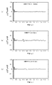
- FIG. 14A As a simulation result, as shown in FIG. 14A, it was confirmed that the received voltage waveform in the piezoelectric element 10 increased from the timing around 340 ns. As a result, it was found that the S/N ratio was smaller than the target value of 28 dB.
- the transmitted wave reaches the center of the main surface of the integrated circuit chip 200 at time 240 ns, as shown in FIG. 10(a). After that, at time 400 ns, as shown in FIG. Waves and the like that pass through and propagate are mixed.
- the wavefront of the reflected wave reflected by the main surface of the integrated circuit chip 200 does not reach the vicinity of the piezoelectric element 10 .
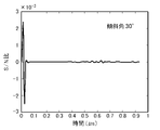
- the received voltage waveform of the piezoelectric element 10 when the chip main surface inclination angle ⁇ is 30° is also at the time when the reflected wave is assumed to re-input to the piezoelectric element 10 as shown in FIG. 14D. It was confirmed that there was almost no increase. As a result, it was found that the S/N ratio reached the target value of 28 dB or more.
- the transmitted wave reaches the center of the main surface of the integrated circuit chip 200 at time 260 ns, as shown in FIG. 11(a). After that, at time 400 ns, as shown in FIG. Waves and the like that pass through and propagate are mixed.
- the reflected wave reflected by the main surface of the integrated circuit chip 200 is directed upward of the integrated circuit chip 200 and the wave front of the reflected wave does not reach the vicinity of the piezoelectric element 10 .
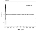
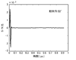
- the received voltage waveform of the piezoelectric element 10 when the chip main surface inclination angle ⁇ is 40° is also at the time when the reflected wave is assumed to re-input to the piezoelectric element 10 as shown in FIG. 14E. It was confirmed that there was almost no increase. As a result, it was found that the S/N ratio reached the target value of 28 dB or more. Although the change in the wavefront when the chip principal surface tilt angle ⁇ is 50° is not shown, the received voltage waveform of the piezoelectric element 10 when the chip principal surface tilt angle ⁇ is 50° is also shown in FIG. 14F. Furthermore, it was confirmed that there was almost no increase even at the time when the reflected wave is assumed to re-enter the piezoelectric element 10 . As a result, it was found that the S/N ratio reached the target value of 28 dB or more.
- the transmitted wave reaches the front end of the main surface of the integrated circuit chip 200 at time 160 ns, as shown in FIG. 12(a). After that, at time 260 ns, as shown in FIG. Propagating waves are mixed. On the other hand, the reflected wave reflected near the edge of the main surface of the integrated circuit chip 200 reaches the vicinity of the piezoelectric element 10 .
- the received voltage waveforms of the piezoelectric element 10 when the chip main surface inclination angle ⁇ is 30°, 40°, and 50° are shown in FIGS. Even at the time when it is supposed to be re-input to the element 10, there is almost no increase. As a result, it was found that the target value of the S/N ratio of 28 dB or more can be achieved by setting the chip main surface inclination angle ⁇ of the integrated circuit chip 200 used as the stealth amplifier 200a in the range of 30° or more and 60° or less. rice field. Furthermore, by performing simulations with different chip main surface inclination angles ⁇ , the relationship between the chip main surface inclination angles ⁇ and the S/N ratios can be obtained as shown in FIG. 15 . It should be noted that the horizontal axis of FIG. 15 expresses the chip main surface tilt angle ⁇ as "chip rotation angle ⁇ (tilt angle)".
- the wavefront of the ultrasonic waves propagating inside the resin horns (300, 301) of the ultrasonic receiver actually has a curved surface or a plurality of wavefronts. It may be a mixture of waves.
- the target ultrasonic wavefront is a curved surface, there are a plurality of tangent planes to the curved wavefront. Therefore, when the wavefront reaching the integrated circuit chip 200 is curved, there are a plurality of chip main surface inclination angles ⁇ with respect to the main surface of the integrated circuit chip 200 exposed to the ultrasonic waves.
- the tangential plane having the smallest angle among the plurality of tilt angles defined by the main surface of the integrated circuit chip 200 is selected, and the plane shown in FIG. Determines the minimum angle of the horizontal axis. That is, when the wavefront of the transmitted wave reaching the integrated circuit chip 200 is a curved surface, the minimum angle shown on the horizontal axis of FIG. In some cases, the target S/N ratio of 28 dB or better is obtained.
- the piezoelectric element 10 and the stealth amplifier 200a are integrated and fixed inside the resin horn parts (300, 301). It is possible to realize a structure and provide an ultrasonic receiver and an ultrasonic observation device with high sensitivity and high S/N ratio.
- a PVDF film having good acoustic impedance matching with water can be used for the piezoelectric element 10, and even when a PVDF film is used, the input connection parasitic capacitance C stray can be reduced.
- a high-sensitivity, high-S/N-ratio hydrophone and an ultrasonic observation device using this hydrophone, which have been long-awaited for measuring minute ultrasonic waves emitted by medical ultrasonic equipment by utilizing pulse response characteristics. can provide.
- the ultrasonic receiver according to the second embodiment of the present invention has a tapered resin tip having a sound field detection axis AX parallel to the traveling direction of ultrasonic waves as a central axis.
- horn parts (300, 301) the piezoelectric element 10 provided with a part exposed at the tip of the horn parts (300, 301), and the inside of the horn parts (300, 301).
- input connection means for electrically connecting between the stealth amplifier 200b arranged at a position shifted from the rear area where the outer shape of the piezoelectric element 10 is projected, and the piezoelectric element 10 and the stealth amplifier 200b.
- the stealth amplifier 200b is arranged in the vicinity of the piezoelectric element 10 at a distance corresponding to the set shortest distance d opt determined as a distance that can be set in terms of design based on equation (3).
- the stealth amplifier 200b amplifies the electrical signal generated by the piezoelectric element 10 through electroacoustic conversion, and prevents the reflected wave of the ultrasonic wave from entering the piezoelectric element 10. It is set so that the wavefront is not uniformly input to the main surface of the piezoelectric layer 101 because the wavefront has a certain angle or more with respect to the surface.
- the piezoelectric element 10 has a plate-like piezoelectric layer 101 such as a PVDF film, and a first electrode plate 111 and a second electrode plate 112 that sandwich the piezoelectric layer 101 .
- the first electrode plate 111 connected to the outer surface of the piezoelectric layer 101 is connected to the input pad (ground side) provided on the main surface (front surface) of the integrated circuit chip constituting the stealth amplifier 200b through the resin ground wiring 311. ) 211 .
- a second electrode plate 112 connected to the inner surface of the piezoelectric layer 101 is connected to an input pad (signal side) 212 provided on the main surface of the integrated circuit chip that constitutes the stealth amplifier 200b via a resin signal wiring 312. Connected.
- the stealth amplifier 200b monolithically integrates circuit elements forming an amplifier circuit (preamplifier).
- the main body (300, 301, 800) extends along the axial direction toward the distal end side in the same manner as shown in FIG. 3A. It has an external terminal 500 on the opposite end side.
- the external terminal 500 is a terminal connected to the observation device 520 via a transmission line 510 such as a coaxial cable, as shown in FIG. 3B.
- the space between the other radial end (lower end) of 10 and an imaginary line 902 extending in the axial direction is defined as a “back region”.
- the stealth amplifier 200b is arranged in the vicinity of the piezoelectric element 10 at a position away from the back region and at a set shortest distance d opt from the piezoelectric element 10.
- the set shortest distance d opt between the piezoelectric element 10 and the stealth amplifier 200b is determined by the input connection means ( It is set to an optimum value in consideration of the input connection parasitic capacitance C stray of the resin signal wiring) 312 .
- the stealth amplifier 200a since the stealth amplifier 200a is arranged in the rear region, the stealth amplifier 200a receives a transmitted wave that has passed through the piezoelectric element 10.
- the stealth amplifier 200b is arranged at a position not exposed to the transmitted wave, so the chip main surface inclination angle ⁇ of the stealth amplifier 200b does not need to be 30° or more and 60° or less.
- the stealth amplifier 200b has an offset amount that is a constant distance in the radial direction from the sound field detection axis AX serving as the central axis so as not to receive the transmitted wave from the piezoelectric element 10 as much as possible. It is located at a position shifted by D. For example, if there is a reference position of the stealth amplifier 200b on the sound field detection axis AX, the offset amount D should be at least half the radial size of the piezoelectric element 10 with respect to this reference position.
- the stealth amplifier 200b overlaps the piezoelectric element 10 when the ultrasonic receiver is viewed along the sound field detection axis AX from the tip end in the axial direction. It is placed in a position where it does not As a result, it is possible to suppress the occurrence of reflected waves that contribute as unwanted echoes.
- the stealth amplifier 200b is arranged at a position shifted by the offset amount D in the radial direction from the sound field detection axis AX, which is the central axis, even if a reflected wave is generated by the stealth amplifier 200b,
- the wavefront of the reflected wave is made to have a certain angle or more with respect to the main surface of the piezoelectric layer 101 constituting the piezoelectric element 10 so that the wavefront of the reflected wave cannot be uniformly incident on the main surface of the piezoelectric layer 101. can.
- the piezoelectric layer 101 is exposed to the positive sound pressure and the piezoelectric layer 101 is exposed to the negative sound pressure.
- the electromotive force generated by electroacoustic conversion is canceled, and the electromotive force can be reduced to a small value.
- An ultrasonic observation apparatus can be configured by including an external terminal provided on the side, a transmission line connected to the external terminal, and an observation device connected by the transmission line.
- the transmission line has an external connection parasitic capacitance C ext that is at least 50 times as large as the signal source capacitance C signal of the piezoelectric element 10, such as an external connection parasitic capacitance C ext , like a coaxial cable.
- the input connection parasitic capacitance C stray has a value smaller than 1/10 of the external connection parasitic capacitance C ext , such as C ext /20, C ext /50, or even C ext /.
- the shortest set distance d opt is 100 or less, the S/N ratio of the ultrasonic receiver and ultrasonic observation apparatus according to the second embodiment can be improved.
- the main body (300, 301, 800) is continuous with the resin horn portion (300, 301) and the thicker diameter side of the resin horn portion (300, 301), and has a two-step structure with the right side being thicker.
- the diameter of the resin columnar portion having a two-step structure can be increased, so that the stealth amplifier 200b and the external terminal 500 can be electrically connected. It is relatively easy to reduce the value of the output connection parasitic capacitance Cout that is parasitic on the output connection means 437. Also, by shortening the distance between the stealth amplifier 200b and the external terminal 500, the value of the output connection parasitic capacitance C out of the ultrasonic receiver according to the second embodiment can be reduced. Furthermore, if the output voltage of the piezoelectric element 10 can be amplified to a sufficiently high voltage by the stealth amplifier 200b, the disadvantage due to the contribution of the output connection parasitic capacitance Cout can be ignored.
- the metal cylindrical housing 800 is filled with an insulating epoxy resin 300 for fixing the positional relationship between the piezoelectric element 10 and the stealth amplifier 200b.
- the cylindrical housing 800 is not arranged at or near the tip of the ultrasonic receiver where the piezoelectric element 10 is arranged. According to the ultrasonic receiver and ultrasonic observation apparatus according to the second embodiment, even if the piezoelectric element 10 and the stealth amplifier 200b are compactly incorporated in the main body (300, 301, 800), the stealth amplifier Since the problem of reflected waves contributing as unwanted echoes from 200b can be resolved, it is possible to improve the reception voltage sensitivity and the S/N ratio.
- the edge of the top surface of the integrated circuit chip 200 is reached at the edge of the back area.
- the transmitted wave reaches the vicinity of the central portion of one main surface (upper surface) of the integrated circuit chip 200, as shown in FIG. 18(b).
- FIG. 20 the relationship shown in FIG. 20 was obtained as the relationship between the offset amount D and the S/N ratio of the stealth amplifier 200b. According to the results of FIG. 20, it can be seen that the S/N ratio target value of 28 dB or more can be obtained in the range where the offset amount D is 0.27 mm or more.
- the piezoelectric element 10 and the stealth amplifier 200b are integrated and fixed inside the resin horn parts (300, 301) to form a compact structure.
- the ultrasonic receiver according to the first modification of the second embodiment of the present invention has a sound field parallel to the traveling direction of ultrasonic waves, as shown in FIGS. 21A and 21B.
- a resin horn portion (300, 301) having a detection axis AX as a central axis and a tapered tip shape, and a piezoelectric element 10 provided with a part exposed at the tip of the resin horn portion (300, 301).
- the stealth amplifier 200c is arranged in the vicinity of the piezoelectric element 10 at a distance corresponding to the set shortest distance d opt determined as a distance that can be set in terms of design based on equation (3).
- the stealth amplifier 200c amplifies the electrical signal generated by the piezoelectric element 10 by electroacoustic conversion, and the reflected wave of the ultrasonic wave does not enter the piezoelectric element 10, or the wavefront of the piezoelectric layer 101 constituting the piezoelectric element 10 By having a certain angle or more with respect to the main surface, the wavefront is set so as not to uniformly enter the piezoelectric element 10 .
- the target S/N ratio value cannot be achieved.
- the reason why the target value of the S/N ratio cannot be achieved is the influence of any of the four side surfaces or the other main surface of the stealth amplifier 200b that forms a cube. This is because the In the ultrasonic receiver according to the first modification of the second embodiment, as shown in FIGS.
- the stealth amplifier 200c is offset, and the four integrated circuit chips constituting the stealth amplifier 200c
- the side surface hereinafter referred to as the "closest side surface 201c" which is located closest to the piezoelectric element 10 and whose longitudinal direction is the parallel direction of the first electrode plate 111 among the side surfaces, the chip main portion is cut off.
- the plane inclination angle ⁇ is 0° or 180°, the effect of improving the S/N ratio can be obtained at all angles.
- the closest side surface 201c of the integrated circuit chip forming the stealth amplifier 200c is chamfered at a predetermined chamfer angle ⁇ with respect to the main surface of the integrated circuit chip. For example, if the main surface of the integrated circuit chip is the (100) plane, the angle measured in the acute direction between the (100) plane and the (111) plane is 55°. The closest side surface 201c can be easily obtained as a cleaved surface.
- the stealth amplifier 200c is configured by defining the taper angle ⁇ of the closest side surface 201c with respect to the direction of the tangential plane of the wavefront of the ultrasonic wave reaching the stealth amplifier 200c, that is, the direction of the main surface of the first electrode plate 111.
- the taper angle ⁇ becomes a complementary angle of the chamfer angle ⁇ .
- the chip main surface inclination angle ⁇ of the integrated circuit chip constituting the stealth amplifier 200c is 90°, 30° ⁇ 60° is preferable. That is, in the ultrasonic receiver according to the first modification of the second embodiment defined by the chip main surface inclination angle ⁇ shown in FIGS.
- the tangential surface 201c is set to a taper angle ⁇ within a range of 30° or more and 60° or less with respect to the tangential plane of the wavefront of the ultrasonic wave reaching the stealth amplifier 200c.
- reflected waves from the main surface and waves propagating through the integrated circuit chip 200j are mixed. Furthermore, at time 220 ns, it is shown that the curved surface reflected wave reflected near the end where the nearest side surface of the integrated circuit chip 200j intersects the main surface starts propagating toward the vicinity of the piezoelectric element 10. .
- the reflected wave from the main surface in the direction orthogonal to the transmitted wave and the original transmitted wave are mixed, and the wave that propagates through the integrated circuit chip 200j is also mixed.
- the transmitted wave moves along the slope of the principal surface and reaches the position of the end on the opposite side of the principal surface.
- the reflected wave from the main surface in the direction orthogonal to the transmitted wave and the original transmitted wave are mixed, and the wave that propagates through the integrated circuit chip 200j is also mixed.
- the transmitted wave reaches a position beyond the end on the opposite side of the main surface, and circulates to the back side of the side surface opposite to the nearest side surface.
- the reflected wave from the main surface in the direction orthogonal to the transmitted wave and the original transmitted wave are mixed, and the wave that propagates through the integrated circuit chip 200j is also mixed.
- the wave reflected by the main surface 200j forming the slope sequentially forms reflected wavefronts as the transmitted wave transmitted through the piezoelectric element 10 advances.
- the inclination of the chip main surface is such that the reflected wavefront from the slope formed by the main surface of the integrated circuit chip 200j does not adversely affect the piezoelectric element 10. It is possible by controlling the angle ⁇ .
- the chamfer angle ⁇ of the integrated circuit chip used for the stealth amplifier 200c is set to 30° ⁇ 60°, and the stealth amplifier 200c is set to the offset position. Due to this arrangement, it is possible to avoid adversely affecting the piezoelectric element 10 by curved reflected waves from the corners where the nearest side surface of the integrated circuit chip 200j intersects the main surface.
- the main surface of the stealth amplifier 200c exposed to the transmitted wave that has passed through the piezoelectric element 10 is the first main surface (surface) of the stealth amplifier 200c or the first main surface (surface) of the stealth amplifier 200c. 2 main surface (back surface).
- the chip main surface inclination angle ⁇ defined with respect to the first or second main surface is set to 90°. Also, when viewed in the vertical cross section of FIG. are shifted by an offset amount D, which is more than half of .
- the stealth amplifier 200c of the ultrasonic receiver according to the first modification of the second embodiment is arranged at a position that does not overlap the piezoelectric element 10 when the ultrasonic receiver is viewed from the distal end side in the axial direction. It is
- the chamfer angle ⁇ of the integrated circuit chip used for the stealth amplifier 200c is set to 30° ⁇ 60°, and the stealth amplifier 200c is displaced from the sound field detection axis AX by an offset amount D, thereby eliminating the need for It is possible to suppress the occurrence of reflected waves that contribute as echoes.
- the chamfer angle ⁇ is set to 30° ⁇
- the wavefront has an angle with respect to the main surface of the piezoelectric layer 101 constituting the piezoelectric element 10, and the wavefront is The signals can be uniformly propagated in directions in which they are not input, and as a result, the S/N ratio can be improved.
- a profile of sound pressure intensity is shown indicating that the wave has reached the nearest side of the tapered shape.
- FIG. 25 shows the relationship with the S/N ratio.
- FIG. 25 shows that the greater the offset amount D, the greater the effect of improving the S/N ratio.
- the target S/N ratio of 28 dB or more is obtained by tapering the closest side surface 201c with a chamfering angle ⁇ of 45°.
- the effect on the S/N ratio is minimized by adding the offset amount D and tapering the closest side surface 201c. can be kept to a limit.
- the main body (300, 301, 800) of the ultrasonic receiver whose right side is thickened by, for example, a two-step structure or the like, and the other end of the main body (300, 301, 800)
- An ultrasonic observation apparatus is configured by including an external terminal provided on the side, a transmission line connected to the external terminal, and an observation device connected by the transmission line. can.
- the transmission line has an external connection parasitic capacitance C ext that is at least 50 times greater than the signal source capacitance C signal of the piezoelectric element 10 like a coaxial cable.
- connection parasitic capacitance C ext has a value of about 10 pF
- the set shortest distance d opt is set so that the input connection parasitic capacitance C stray is smaller than 1/10 of the external connection parasitic capacitance C ext , for example, C ext It can be set to a value of about /100.
- the main body (300, 301, 800) is continuous with the resin horn portion (300, 301) and the thicker diameter side of the resin horn portion (300, 301), and has a two-step structure, and the right end side is thicker.
- the ultrasonic receiver according to the second modification of the second embodiment of the present invention has, as a central axis, a sound field detection axis AX parallel to the traveling direction of ultrasonic waves, and has a tapered tip.
- the stealth amplifier 200d is arranged at a position shifted from the rear area where the outer shape of the piezoelectric element 10 is projected, and the input connection means (resin signal signal wiring) 312 .
- the stealth amplifier 200d is arranged in the vicinity of the piezoelectric element 10 at a distance corresponding to the set shortest distance d opt determined as a distance that can be set in terms of design based on equation (3).
- the stealth amplifier 200d amplifies the electrical signal generated by the piezoelectric element 10 through electroacoustic conversion, so that the reflected wave of the ultrasonic wave does not enter the piezoelectric element 10, or even if the reflected wave is generated, the wavefront of the piezoelectric element 10 is uniform. It is set not to enter.
- a normal integrated circuit chip having four vertical side walls is used as a stealth amplifier 200d.
- the stealth amplifier 200d of the ultrasonic receiver according to the second modification of the second embodiment has an offset amount D in the radial direction from the sound field detection axis AX serving as the central axis so as not to receive the transmitted wave from the piezoelectric element 10. It is placed in a position that has moved only Furthermore, as shown in FIG. 26, the chip main surface inclination angle ⁇ of the integrated circuit chip used as the stealth amplifier 200d is set to 120°, which is larger than 90°.
- FIG. 27(c) shows the case where the chip main surface tilt angle ⁇ of the stealth amplifier 200d is 120° and the offset amount D is 0.4 mm. It reaches the end where the main surface (surface) and the nearest side meet at 90°.
- a reflected wave from the first main surface, a wave that propagates through the stealth amplifier 200d, and the like are mixed.
- the downward direction which is the radial direction of the sound field detection axis AX as the central axis, is defined as the "plus direction”. Further, from FIG. 29, when the chip main surface inclination angle ⁇ is maintained at 120° and offset in the negative direction, the target value of the S/N ratio of 28 dB or more can be obtained in the range of the offset amount D ⁇ 0.05 mm. It is understood that In FIG. 26, moving upward perpendicular to the sound field detection axis AX is the "minus direction".
- the piezoelectric element 10 is arranged on the left side, the main body (300, 301, 800) of the ultrasonic receiver whose right side is thickened by a two-step structure or the like, and the main body (300, 301, 800) by providing an external terminal provided on the other (right) end side, a transmission line connected to the external terminal, and an observation device connected by the transmission line.
- An ultrasonic observation apparatus according to a second modification of the embodiment can be configured.
- the transmission line is 50 times or more the signal source capacitance C signal of the piezoelectric element 10, further, for example, 100 times or more, or 1000 times or more.
- the set shortest distance d opt may can be set to a value smaller than 1/10 of , for example, a value of about C ext /100.
- the stealth amplifier 200d and the external terminal 500 are separated.
- the value of the output connection parasitic capacitance C out that is parasitic on the output connection means that electrically connects between them can be reduced.
- the value of the output connection parasitic capacitance C out of the ultrasonic receiver according to the second modification of the second embodiment. 10 can be amplified to a sufficiently high voltage by the stealth amplifier 200d, the penalty due to the output connection parasitic capacitance C out is negligible.
- the input connection parasitic capacitance C stray can be reduced and excellent pulse response characteristics can be utilized. Therefore, according to the ultrasonic receiver according to the second modified example of the second embodiment, ultrasonic waves suitable for medical purposes with high sensitivity and a high S/N ratio that can measure minute ultrasonic waves A receiver and an ultrasound observation device can be provided.
- the piezoelectric element 10 of the ultrasonic receiver includes a piezoelectric layer 101, and a first electrode plate 111 and a first electrode plate 111 sandwiching the piezoelectric layer 101. and two electrode plates 112 .
- the stealth amplifier 200f has a virtual line 903 extending axially from one radial end (top end) of the piezoelectric element 10 and an axial line 903 extending axially from the other radial end (bottom end) of the piezoelectric element 10.
- the stealth amplifier 200f is arranged radially shifted by an offset distance D from the sound field detection axis AX located on the center axis so as not to receive the transmitted wave from the piezoelectric element 10 as much as possible.
- the offset distance D By moving by the offset distance D, it is possible to suppress the generation of reflected waves that may re-input to the piezoelectric element 10, and even if the reflected waves are generated, they are not input to the piezoelectric element 10 again, resulting in S/ It can be expected that the N ratio can be improved.
- the main surface of the integrated circuit chip constituting the stealth amplifier 200f exposed to the transmitted wave transmitted through the piezoelectric element 10 is the first main surface (surface) of the integrated circuit chip. be.
- a second electrode plate 112 connected to the inner side of the piezoelectric layer 101 is connected to an input pad (signal side) 212 of the stealth amplifier 200f via an L-shaped resin signal wiring 312f.
- the stealth amplifier 200f has an amplifier (stealth amplifier 200f).
- the stealth amplifier 200f also includes a chip-side ground pad 221 for receiving a ground potential from the external terminal 500, and a chip-side ground pad 221 for outputting a signal amplified by an amplifier circuit integrated in the integrated circuit chip at the external terminal 500.
- An output pad 222 and a chip-side power supply pad 223 for receiving a power supply potential from an external terminal 500 are provided.
- a stealth amplifier 200f that constitutes an ultrasonic receiver according to a comparative example of the third embodiment is mounted on a printed circuit board 400.
- the printed circuit board 400 includes a relay ground pad 411 and an external ground pad 421 corresponding to the chip-side ground pad 221 of the stealth amplifier 200f, and a relay output pad 412 and an external output pad 422 corresponding to the chip-side output pad 222 of the stealth amplifier 200f. , a relay power supply pad 413 and an external power supply pad 423 corresponding to the chip-side power supply pad 223 of the stealth amplifier 200f.
- the chip-side ground pad 221 and the relay ground pad 411 are connected to each other by a conductive wire (ground wire) 231 such as an Au (gold) wire, and the external ground pad 421 is connected by a conductive wire (ground lead wire) 431 such as an Au wire. It is connected to the external terminal of the ultrasonic receiver.
- the chip-side output pads 222 and relay output pads 412 are connected to each other by conductive wires (output wires) 232 such as Au wires, and the external output pads 422 are connected to output connection means (output lead wires) 432 such as Au wires. is connected to the external terminal 500 of the ultrasonic receiver (see FIG. 3A).
- the chip-side power pads 223 and relay power pads 413 are connected to each other by conductive wires (power wires) 233 such as Au wires, and the external power pads 423 are interconnected by conductive wires (power lead wires) 433 such as Au wires. It is connected to the external terminal of the sound wave receiver.
- the chip main surface inclination angle ⁇ of the stealth amplifier 200f is set to 90°.
- the closest side surface of the integrated circuit chip forming the stealth amplifier 200f is chamfered at a predetermined taper angle ⁇ . That is, the nearest side surface of the integrated circuit chip forming the stealth amplifier 200f is set to a taper angle ⁇ of 30° ⁇ 60°.
- the metal tubular housing 800 is filled with an insulating epoxy resin 300 for fixing the positional relationship between the piezoelectric element 10 and the stealth amplifier 200f.
- the cylindrical housing 800 is not arranged at or near the tip of the ultrasonic receiver where the piezoelectric element 10 is arranged.
- the ultrasonic receiver according to the comparative example of the third embodiment even if the piezoelectric element 10 and the stealth amplifier 200f are compactly incorporated in the main body (300, 301, 800), the Since the problem of reflected waves that may contribute as unnecessary echoes from the amplifier 200f can be resolved, it is expected that the reception voltage sensitivity will be improved and the S/N ratio will be improved. However, as shown in FIGS. 31A and 31B, reflected waves from the ground lead 431, the output lead (output connection means) 432, and the power lead 433 are generated, which affects the S/N ratio. be.
- FIG. 31A shows changes over time in the sound pressure intensity profile of ultrasonic waves in the structure of the ultrasonic receiver according to the comparative example of the third embodiment shown in FIGS. 30A and 30B.
- the transmitted wave reaches a position behind the output lead wire (output connection means) 432 .
- the reflected wave from the output lead wire (output connection means) 432 reaches the vicinity of the central portion of the first main surface (upper surface) of the integrated circuit chip constituting the stealth amplifier 200f.
- FIG. 31B shows the received voltage waveform observed by the piezoelectric element 10 of the ultrasonic receiver according to the comparative example of the third embodiment.
- the reflected wave (echo) from the Au wire appears from around 580 ns and continues until around 950 ns.
- the S/N ratio of the ultrasonic receiver according to the comparative example of the third embodiment was 29 dB.
- the S/N ratio of 29 dB which is equal to or higher than the target value of 28 dB, was obtained by setting the taper angle ⁇ to 30° ⁇ 60°.
- the output connection means (output lead wire) 432 connecting the stealth amplifier 200f and the external terminal 500 of the ultrasonic receiver a reflected wave from the output connection means 432 is generated, and the S/N ratio is reduced. have a bad influence.
- the external connection lead wire (ground lead wire) 431 and the external connection lead wire (power lead wire) line) 433 is generated and adversely affects the S/N ratio. Therefore, it is effective to dispose the screen member 320 as shown in FIG.
- the ultrasonic receiver according to the third embodiment includes a resin horn portion (300, 301) having a tapered tip, which has a sound field detection axis AX parallel to the traveling direction of ultrasonic waves as a central axis, and this Piezoelectric element 10 partially exposed at the tip of the resin horn part (300, 301), and inside the resin horn part (300, 301), behind the projection of the outer shape of the piezoelectric element 10
- a stealth amplifier 200f is arranged at a position shifted from the region.
- the stealth amplifier 200f is arranged in the vicinity of the piezoelectric element 10 at a distance corresponding to the set shortest distance d opt determined as a distance that can be set in terms of design based on equation (3).
- the stealth amplifier 200f amplifies the electrical signal generated by the piezoelectric element 10 through electroacoustic conversion, and the reflected wave of the ultrasonic wave does not enter the piezoelectric element 10, or the wavefront of the reflected wave forms the piezoelectric element 10. It is set so that the main surface of the body layer 101 is not uniformly input to the piezoelectric element 10 .
- the presence of the input connecting means (resin signal wiring) and the resin grounding wiring for electrically connecting the piezoelectric element 10 and the stealth amplifier 200f is the first reason.
- the ultrasonic receiver according to the third embodiment differs from the ultrasonic receiver according to the comparative example of the third embodiment in that a screen member 320 having a flat stealth surface as a main surface is mounted on a printed circuit board 400. has improved characteristics.
- Other structures of the ultrasonic receiver according to the third embodiment are the same as those of the ultrasonic receiver according to the comparative example of the third embodiment. Therefore, the screen member 320 will be described below, and other components will be described in detail by assigning the same reference numerals as those used in the description of the ultrasonic receiver according to the comparative example of the third embodiment. omitted.
- the direction of the stealth surface forming the main surface of the screen member 320 of the ultrasonic receiver according to the third embodiment is inclined by the “screen tilt angle ⁇ ” defined with respect to the direction of the main surface of the first electrode plate 111 .
- the screen inclination angle ⁇ is set within the range of 30° ⁇ 60°.
- the lower limit value of 30° for the screen inclination angle ⁇ is the same as the lower limit value for the chip main surface inclination angle ⁇ described above. The same is true for improvement.
- the upper limit of the screen inclination angle ⁇ of 60° eliminates the influence of the reflected wave, which may contribute as an unwanted echo generated by itself, on the S/N ratio, and is located behind the screen member 320 (external terminal 500 side), the ground lead wire (external connection lead wire) 431 such as Au wire, the output lead wire (output connection means) 432, and the power supply lead wire (external connection lead wire) 433 are prevented from being hit by ultrasonic waves.
- This angle is determined as a necessary condition.
- the stealth surface of the screen member 320 prevents the ground lead wire 431, the output lead wire (output connection means) 432, and the power lead wire 433 behind it. Since there is no reflected wave, even if the piezoelectric element 10 and the stealth amplifier 200f are compactly incorporated in the main body (300, 301, 800), the reception voltage sensitivity is improved and the S/N ratio is improved. be able to.
- the ground wire 231 such as an Au wire, the output wire 232, and the power wire 233 located in front of the screen member 320, that is, on the side of the piezoelectric element 10, are reflected from these wires.
- the resin ground wiring 311f and the resin signal wiring (input connecting means) 312f are also arranged at a position outside the area behind the piezoelectric element 10 when the ultrasonic receiver is viewed from the tip end in the axial direction.
- the ground lead wire 431, the output lead wire (output connection means) 432, and the power lead wire 433 also have It is preferably located away from the area behind the piezoelectric element 10 .
- FIG. 33A shows changes over time in the sound pressure intensity profile of ultrasonic waves in the structure of the ultrasonic receiver according to the third embodiment shown in FIG.
- time 520 ns is the timing at which the transmitted wave reaches a position behind the output lead wire (output connecting means) 432 when the screen member 320 is not present.
- a plurality of reflected waves including the reflected wave from the stealth surface of the partition member 320 are propagated toward a position above the piezoelectric element 10 and away from the piezoelectric element 10 .
- the wavefront of the reflected wave of the curved wave reflected at the boundary between the top surface of the integrated circuit chip constituting the stealth amplifier 200f and the nearest side surface chamfered at the taper angle ⁇ is also above the top surface of the integrated circuit chip. are present and mixed. Furthermore, a transmitted wave that has passed through the integrated circuit chip that constitutes the stealth amplifier 200f also exists on the second main surface (back surface) side of the integrated circuit chip.
- FIG. 33B shows the received voltage waveform observed by the piezoelectric element 10 of the ultrasonic receiver according to the third embodiment.
- the influence of the reflected wave from the Au wire appeared from around 580 ns and continued until around 950 ns.
- the ultrasonic receiver according to No. 2 although there was some influence of reflected waves from the stealth surface of the screen member 320, no reflected waves from the Au wire were observed.
- the S/N ratio of the ultrasonic receiver according to the third embodiment was 32 dB, which was found to be improved from 29 dB of the ultrasonic receiver according to the comparative example of the third embodiment.
- the third An ultrasonic observation apparatus can be configured.
- the transmission line is 50 times or more, for example, 100 times or more, or 1000 times or more as large as the signal source capacitance C signal of the piezoelectric element 10 like a coaxial cable.
- connection parasitic capacitance C ext has a value of, for example, the external connection parasitic capacitance C ext ⁇ 10 pF
- the set shortest distance d opt is set so that the input connection parasitic capacitance C stray is 1/10 of the external connection parasitic capacitance C ext . can be set to a value smaller than C ext /100, for example.
- the distance between the stealth amplifier 200f and the external terminal is increased.
- the distance between the stealth amplifier 200f and the external terminal is increased.
- the value of the output connection parasitic capacitance C out of the ultrasonic receiver according to the third embodiment can be reduced .
- Value considerations are optional.
- the piezoelectric element 10 and the stealth amplifier 200f are integrally fixed inside the resin horn parts (300, 301), and further Providing an ultrasonic receiver and an ultrasonic observation apparatus suitable for medical purposes, which realizes a compact structure by providing a screen member 320, has excellent pulse response characteristics, high sensitivity, and a high S/N ratio. can.
- the ultrasonic receiver according to the fourth embodiment of the present invention includes a resin horn portion (300, 301) having a tapered tip, which has a sound field detection axis AX as a central axis, and this Piezoelectric element 10 partially exposed at the tip of the resin horn part (300, 301), and inside the resin horn part (300, 301), behind the projection of the outer shape of the piezoelectric element 10 It has a stealth amplifier 200g located in the area. The stealth amplifier 200g is placed in the vicinity of the piezoelectric element 10 at a distance corresponding to the set shortest distance d opt determined as a designable distance based on the piezoelectric element 10 and equation (3).
- the stealth amplifier 200g amplifies the electrical signal generated by the piezoelectric element 10 through electroacoustic conversion, and changes the reflection characteristics of the ultrasonic wave transmitted through the piezoelectric element 10 so that the reflected ultrasonic wave does not enter the piezoelectric element 10.
- the wavefront of the reflected wave is set so as not to uniformly enter the main surface of the piezoelectric layer 101 forming the piezoelectric element 10 .
- the input connection means (resin signal wiring) and the resin ground wiring for electrically connecting the piezoelectric element 10 and the stealth amplifier 200g are omitted from the drawing.
- the thickness t of the semiconductor integrated circuit chip used in the stealth amplifier 200g is 100 ⁇ m or less.
- the changes over time in the sound pressure intensity profile of the ultrasonic waves are observed as shown in FIGS. 35 and 36.
- FIG. When the chip main surface tilt angle ⁇ is 0°, the transmitted wave reaches the main surface of the Si chip at time 240 ns as shown in FIG. 35(a). After that, at time 460 ns, as shown in FIG. be re-entered.
- the reflected wave reflected by the end surface of the Si chip is not observed near the piezoelectric element 10 in the sound pressure intensity profile shown in FIG. 36(b).
- FIG. 37 shows the relationship between the thickness t of the Si chip used for the stealth amplifier 200g and the S/N ratio.
- the thickness t of the Si chip used for the stealth amplifier 200g it is necessary to consider the ease of handling. That is, if the chip thickness t becomes too thin, there will be a problem of chip breakage during mounting, so the chip must be handled carefully, resulting in a reduction in ease of assembly of the ultrasonic receiver. You will lose.
- the S/N ratio can be improved by reducing the thickness t to a predetermined value or less according to the chip main surface inclination angle ⁇ .
- a remarkable effect of improvement can be obtained.
- the piezoelectric element 10 is arranged on the left side, the main body (300, 301, 800) of the ultrasonic receiver whose right side is thickened by a two-step structure or the like, and the main body (300, 301, 800) Ultrasonic observation according to the fourth embodiment by providing an external terminal provided on the other (right) end side, a transmission line connected to the external terminal, and an observation device connected by the transmission line You can configure the device.
- the transmission line is 50 times or more, for example, 100 times or more, or 1000 times or more as large as the signal source capacitance C signal of the piezoelectric element 10 like a coaxial cable.
- the parasitic capacitance C ext has a value of, for example, the external connection parasitic capacitance C ext ⁇ 10 pF
- the set shortest distance d opt is such that the input connection parasitic capacitance C stray is less than 1/10 of the external connection parasitic capacitance C ext . is also set to a small value, for example, a value of about C ext /100.
- the distance between the stealth amplifier 200g and the external terminal is increased.
- the ultrasonic receiver and the ultrasonic observation apparatus even when a PDVF film having good acoustic impedance matching with water is used, a stealth sensor composed of an integrated circuit chip with a thin plate thickness is used.
- a compact structure can be realized in which the amplifier 200g and the piezoelectric element 10 are integrally fixed inside the resin horn portion (300, 301) so as to reduce the input connection parasitic capacitance.
- the ultrasonic receiver according to the fifth embodiment of the present invention includes a resin horn portion (300, 301) having a tapered tip, which has a sound field detection axis AX as a central axis, and this Piezoelectric element 10 partially exposed at the tip of the resin horn part (300, 301), and inside the resin horn part (300, 301), behind the projection of the outer shape of the piezoelectric element 10 It has a stealth amplifier 200h located in the area. The stealth amplifier 200h is placed in the vicinity of the piezoelectric element 10 at a distance corresponding to the set shortest distance d opt determined as a designable distance based on the piezoelectric element 10 and equation (3).
- the stealth amplifier 200h amplifies the electrical signal generated by the piezoelectric element 10 through electroacoustic conversion, and changes the reflection characteristics of the ultrasonic wave transmitted through the piezoelectric element 10 so that the reflected ultrasonic wave does not enter the piezoelectric element 10.
- the stealth amplifier 200h made of a polymer material is provided so that the wavefront is not uniformly input to the main surface of the piezoelectric layer 101 forming the piezoelectric element 10 even if a reflected wave is generated.
- the stealth amplifier 200h is made of an ultrasonically transparent polymer material so that the acoustic impedance of the stealth amplifier 200h is equal to the acoustic impedance of the insulating resin 300, the inclination angle ⁇ of the chip main surface, the chip thickness t, etc.
- the problem of unnecessary echo generation due to reflected waves can be easily solved regardless of the For example, in recent years, chips made of polymer materials such as organic semiconductors such as polyimide substrates have been developed. Organic semiconductors have the property of transmitting ultrasonic waves more than general Si substrates. Therefore, there is no need to consider the inclination angle ⁇ of the chip main surface, the chip thickness t, etc., and the problem of unnecessary echo generation due to reflected waves can be eliminated. Solvable.
- the chip made of polymer material used in the ultrasonic receiver according to the fifth embodiment of the present invention means "polymer material" in a broad sense. If configured, the active area, in which active devices, etc. that function as amplifiers are formed, need not be organic.
- the active region may be, for example, a semiconductor layer surrounded by an element isolation region like a frame. Even in the case of a composite structure of a semiconductor layer and a polymeric material layer, if the thickness of the active region is less than 1 ⁇ m, acoustically, the ultrasonic waves pass through the active region and the thin film of the polymeric material, and most of the reflected waves are generated.
- the chip made of a polymer material can be set to not As the chip made of a polymer material, a polyimide substrate, a polyethylene naphthalate substrate, an epoxy substrate made by a varnish method, a substrate made of a material similar in acoustic characteristics to epoxy resin, and the like can be used.
- the stealth amplifier 200h of the ultrasonic receiver according to the fifth embodiment is made of a polymer material that transmits ultrasonic waves, unwanted echoes due to reflected waves can Problems that arise can be easily resolved.
- FIG. When the chip main surface tilt angle ⁇ is 0°, the transmitted wave reaches the first main surface of the organic semiconductor chip at time 240 ns, as shown in FIG. 39(a). After that, at time 340 ns, as shown in FIG.
- the transmitted wave passes through the first main surface of the organic semiconductor chip and reaches the second main surface.
- a weak reflected wave (unwanted echo) starts propagating toward the piezoelectric element 10 .
- time 240 ns as shown in FIG.
- There are mixed waves such as reflected waves from the main surface and waves that pass through the inside of the organic semiconductor chip and propagate rightward.
- the reflected wave reflected by the nearest side surface of the organic semiconductor chip also starts propagating toward the piezoelectric element 10 in the sound pressure intensity profile shown in FIG. 40(b).
- Changes in the received voltage waveform measured by the piezoelectric element 10 shown in FIG. 41(b) corresponds to the temporal change in the sound pressure intensity profile inside the resin horn parts (300, 301) shown in FIG.
- the S/N ratio can be improved to about 25 dB by using an organic semiconductor chip as the stealth amplifier 200h.
- the ultrasonic observation apparatus is 50 times or more, for example, 100 times or more, or 1000 times or more as large as the signal source capacitance C signal of the piezoelectric element 10 like a coaxial cable.
- the set shortest distance d opt is set so that the input connection parasitic capacitance C stray is 1/10 of the external connection parasitic capacitance C ext . is also set to a small value, for example, a value of about C ext /100.
- the distance between the stealth amplifier 200h and the external terminal is increased. can be designed to have a low value of the output connection parasitic capacitance C out parasitic on the output connection means electrically connecting the . Furthermore, by shortening the distance between the stealth amplifier 200h and the external terminal, the value of the output connection parasitic capacitance C out of the ultrasonic receiver according to the fifth embodiment can be reduced . Considerations regarding the value of are optional.
- the stealth amplifier 200h by forming the stealth amplifier 200h with a resin having a property of transmitting ultrasonic waves, compared to the case where the stealth amplifier is formed with a Si substrate, , the S/N ratio can be improved.
- a material with an acoustic impedance that allows the stealth amplifier 200h to transmit 100% of ultrasonic waves is developed, there is no need to consider the chip main surface inclination angle ⁇ , the chip thickness t, etc., and the generation of unwanted echoes due to reflected waves. can solve the problem.
- the ultrasonic receiver and the ultrasonic observation apparatus As described above, according to the ultrasonic receiver and the ultrasonic observation apparatus according to the fifth embodiment, even when a PDVF film having good acoustic impedance matching with water is used, the piezoelectric element 10 and the polymer material It is possible to realize a compact structure in which the stealth amplifier 200h composed of the resin is integrated and fixed inside the resin horn parts (300, 301) so as to reduce the input connection parasitic capacitance. Therefore, according to the ultrasonic receiver and the ultrasonic observation apparatus according to the fifth embodiment, an ultrasonic receiver that has excellent pulse response characteristics, high sensitivity, and a high S/N ratio, and is suitable for medical purposes. And an ultrasonic observation device can be provided.
- the present invention has been exemplified using the first to fifth embodiments, but it should be understood that the statements and drawings forming part of this disclosure limit the present invention. is not.
- the main surface of the integrated circuit chip employed as the stealth amplifier is a flat and uniform plane, and the reflection surface for reflecting the transmitted wave is flat.
- the description has been made on the assumption that the reflecting surface is a uniform plane, it is not necessary to limit the reflecting surface to a plane.
- “Plane” means the Euclidean plane with Gaussian curvature and mean curvature always zero.
- An ultrasonic receiver as shown in FIG. Piezoelectric element 10 partially exposed at the tip of the resin horn part (300, 301), and inside the resin horn part (300, 301), behind the projection of the outer shape of the piezoelectric element 10
- the stealth amplifier 200i is arranged in the vicinity of the piezoelectric element 10 at a distance corresponding to the set shortest distance d opt determined as a designable distance based on the piezoelectric element 10 and equation (3).
- the stealth amplifier 200i amplifies the electrical signal generated by the piezoelectric element 10 through electroacoustic conversion, and changes the reflection characteristics of the ultrasonic wave transmitted through the piezoelectric element 10 so that the reflected ultrasonic wave does not enter the piezoelectric element 10.
- it has a non-planar reflecting surface which is set so that even if a reflected wave is generated, the wavefront is not uniformly input to the main surface of the piezoelectric layer 101 constituting the piezoelectric element 10 .
- Input connection means (resin signal wiring) and resin ground wiring for electrically connecting the piezoelectric element 10 and the stealth amplifier 200i are not shown in the drawings, but the ultrasonic waves according to other embodiments are not shown.
- the main surface of the integrated circuit chip used as the stealth amplifier 200i is non-planar (curved) and the reflection surface for reflecting the transmitted wave is curved.
- Examples of three-dimensional structures in which the reflecting surface that reflects the transmitted wave is a curved surface are generally spheres with positive Gaussian curvature, rugby balls (spheroids), and egg-shaped shapes, and already spherical integrated circuits. The chip has been put to practical use.
- the stealth amplifier 200i is cylindrical, and a two-dimensional simulation is performed using a cross section perpendicular to the central axis of the cylinder as an analysis plane.
- the Gaussian curvature of a cylinder (cylinder) is zero, but the mean curvature is not. Even in the case of a cylindrical integrated circuit chip, a cylindrical integrated circuit chip can be easily realized because lithography technology for curved surfaces has been established. If the Gaussian curvature is negative, it becomes a hyperbolic plane.
- An ultrasonic receiver has a structure as shown in FIG. 42, and the stealth amplifier 200i is arranged on the sound field detection axis AX of the ultrasonic receiver without offset.
- the stealth amplifier 200i is a cylindrical chip with a diameter of approximately 1.0 mm.
- the central axis defining the rotationally symmetrical structure of the cylinder is perpendicular to the plane of the paper.
- the transmitted wave reaches the closest generatrix existing at the position closest to the piezoelectric element 10 on the side surface of the cylindrical chip at time 200 ns.
- a reflected wave propagating toward the piezoelectric element 10 and a transmitted wave passing through the interior of the cylindrical chip and heading toward the farthest generatrix facing the closest generatrix are generated.
- the wavefront of the reflected wave reflected at the position of the closest generatrix of the chip reaches the piezoelectric element 10 .
- the results shown in FIG. 44 were obtained. From FIG. 44, a result of 15 dB was obtained for the S/N ratio. This result is almost the same as the S/N ratio obtained when a square plate-shaped integrated circuit chip with a side of about 1.0 mm is tilted at an inclination angle .theta. of 0.degree. or 90.degree. However, by reducing the size of the cylindrical tip to, for example, about 0.1 mm or less, as in the case where the thickness t of the tip is reduced in the fourth embodiment, the target value of the S/N ratio is 28 dB. The above can be realized.
- the S/N ratio is improved.
- a target value of 28 dB or more can be achieved.
- the size of the cylindrical chip may be reduced and may be offset.
- the stealth amplifier 200i is cylindrical, and a two-dimensional simulation is performed using a cross section perpendicular to the central axis of the cylinder as an analysis plane.
- the stealth amplifier 200i has a spherical shape, the reflected wave propagates in a three-dimensional direction including the direction perpendicular to the page of FIG. Assuming that an ultrasonic wave is first incident on the north pole of a sphere forming a three-dimensional curved surface, the area of the reflected portion increases with the square of the distance from the north pole.
- the spherical surface is used as the reflecting surface, the energy of the ultrasonic waves reflected at the north pole is reduced, improving the S/N ratio.
- the smaller the radius of curvature of the sphere the greater the S/N ratio, and the smaller the radius of curvature, the better.
- the reflected wave propagates while dispersing in three-dimensional directions. Since the ultrasonic waves do not reach the receiver, the effects of the ultrasonic receivers according to the second to fifth embodiments can be exhibited more effectively.
- the shape of the stealth amplifier 200i used in the ultrasonic receiver is not limited to a cylinder or a sphere, and may be a torus (annulus) with a circular inner diameter or a donut shape. If the piezoelectric element 10 is circular, the rear area will be a cylindrical area where the piezoelectric element 10 is projected along the sound field detection axis AX. Therefore, if the stealth amplifier 200i is composed of a torus surrounding the cylindrical rear region, the stealth amplifier 200i can be arranged at a position outside the rear region. When the piezoelectric element 10 is circular, the rear area is a cylindrical projection area formed by translating the outer circumference of the piezoelectric element 10 along the sound field detection axis AX.
- the piezoelectric element 10 and the stealth amplifier 200i having a curved outer shape are combined with the resin horn part. (300, 301) realizes a compact structure that is integrated to reduce the input connection parasitic capacitance, and has excellent pulse response characteristics, high sensitivity, and a high S/N ratio, and can be used for medical purposes.
- a suitable ultrasonic receiver and ultrasonic observation device can be provided.
- the ultrasonic receiver has been mainly described on the premise that it is a hydrophone, but it can also be applied to other ultrasonic receivers having the piezoelectric element 10 .
- the integrated circuit chip may include an integrated circuit having functions other than the amplifier, or may have another function instead of the amplifier. It can be chips. Further, the effect of improving the S/N ratio can be obtained by simply arranging the partition member described in the third embodiment behind the piezoelectric element 10 instead of the integrated circuit chip.
- the S/N ratio derived from FIG. 41 was slightly lower than the target value of 28 dB.
- the technical idea of the ultrasonic receiver according to the fifth embodiment using the polymer material chip may be applied to the ultrasonic receiver according to the first to fourth embodiments or the ultrasonic receiver according to the other embodiments.
- the target value of 28 dB or more can be achieved by applying the concept and using a polymer material chip instead of a semiconductor chip.
- the input connection means for electrically connecting the piezoelectric element and the stealth amplifier is the resin signal wiring. It is not intended to be limited to wiring made of The "input connection means" may be anything as long as it has a function of electrically connecting between various piezoelectric elements such as metal wiring and the stealth amplifier.
- the present invention is not limited to the description of the above-described first to fifth embodiments, and various modifications are possible, which are also included within the scope of the present invention. Needless to say. Therefore, the technical scope of the present invention is defined only by the matters specifying the invention according to the scope of claims that are valid from the above description.
Landscapes
- Engineering & Computer Science (AREA)
- Physics & Mathematics (AREA)
- Remote Sensing (AREA)
- Life Sciences & Earth Sciences (AREA)
- General Physics & Mathematics (AREA)
- Acoustics & Sound (AREA)
- Geology (AREA)
- General Life Sciences & Earth Sciences (AREA)
- Environmental & Geological Engineering (AREA)
- Geophysics (AREA)
- Computer Networks & Wireless Communication (AREA)
- Radar, Positioning & Navigation (AREA)
- Signal Processing (AREA)
- Transducers For Ultrasonic Waves (AREA)
Priority Applications (4)
| Application Number | Priority Date | Filing Date | Title |
|---|---|---|---|
| EP22791801.8A EP4325891A4 (en) | 2021-04-22 | 2022-04-21 | ULTRASOUND RECEIVER AND ULTRASOUND OBSERVATION DEVICE |
| JP2023515524A JP7594249B2 (ja) | 2021-04-22 | 2022-04-21 | 超音波受信器及び超音波観測装置 |
| CN202280030448.0A CN117356109A (zh) | 2021-04-22 | 2022-04-21 | 超声波接收器及超声波观测装置 |
| US18/485,380 US20240036224A1 (en) | 2021-04-22 | 2023-10-12 | Ultrasonic receiver and ultrasonic observation device |
Applications Claiming Priority (2)
| Application Number | Priority Date | Filing Date | Title |
|---|---|---|---|
| JP2021-072856 | 2021-04-22 | ||
| JP2021072856 | 2021-04-22 |
Related Child Applications (1)
| Application Number | Title | Priority Date | Filing Date |
|---|---|---|---|
| US18/485,380 Continuation US20240036224A1 (en) | 2021-04-22 | 2023-10-12 | Ultrasonic receiver and ultrasonic observation device |
Publications (1)
| Publication Number | Publication Date |
|---|---|
| WO2022225030A1 true WO2022225030A1 (ja) | 2022-10-27 |
Family
ID=83722352
Family Applications (1)
| Application Number | Title | Priority Date | Filing Date |
|---|---|---|---|
| PCT/JP2022/018488 Ceased WO2022225030A1 (ja) | 2021-04-22 | 2022-04-21 | 超音波受信器及び超音波観測装置 |
Country Status (5)
| Country | Link |
|---|---|
| US (1) | US20240036224A1 (https=) |
| EP (1) | EP4325891A4 (https=) |
| JP (1) | JP7594249B2 (https=) |
| CN (1) | CN117356109A (https=) |
| WO (1) | WO2022225030A1 (https=) |
Families Citing this family (1)
| Publication number | Priority date | Publication date | Assignee | Title |
|---|---|---|---|---|
| DE102021118641A1 (de) * | 2021-07-20 | 2023-01-26 | Valeo Schalter Und Sensoren Gmbh | Entkopplungselement für einen ultraschallsensor |
Citations (3)
| Publication number | Priority date | Publication date | Assignee | Title |
|---|---|---|---|---|
| JPH01171200U (https=) * | 1988-05-10 | 1989-12-04 | ||
| JPH04132498A (ja) | 1990-09-25 | 1992-05-06 | Olympus Optical Co Ltd | 超音波センサ装置 |
| JPH04218765A (ja) * | 1990-03-26 | 1992-08-10 | Toshiba Corp | 超音波プローブ |
Family Cites Families (6)
| Publication number | Priority date | Publication date | Assignee | Title |
|---|---|---|---|---|
| JPS57171384U (https=) * | 1981-04-21 | 1982-10-28 | ||
| US6108274A (en) * | 1995-12-15 | 2000-08-22 | Innovative Transducers, Inc. | Acoustic sensor and array thereof |
| JP4171052B2 (ja) * | 2006-05-31 | 2008-10-22 | 株式会社東芝 | アレイ式超音波プローブおよび超音波診断装置 |
| JP4947115B2 (ja) * | 2009-09-30 | 2012-06-06 | 株式会社村田製作所 | 超音波トランスデューサ |
| WO2013170150A1 (en) * | 2012-05-11 | 2013-11-14 | Volcano Corporation | Circuit architectures and electrical interfaces for rotational intravascular ultrasound (ivus) devices |
| WO2015064216A1 (ja) * | 2013-10-28 | 2015-05-07 | 株式会社村田製作所 | 圧電センサ |
-
2022
- 2022-04-21 JP JP2023515524A patent/JP7594249B2/ja active Active
- 2022-04-21 WO PCT/JP2022/018488 patent/WO2022225030A1/ja not_active Ceased
- 2022-04-21 CN CN202280030448.0A patent/CN117356109A/zh active Pending
- 2022-04-21 EP EP22791801.8A patent/EP4325891A4/en active Pending
-
2023
- 2023-10-12 US US18/485,380 patent/US20240036224A1/en active Pending
Patent Citations (3)
| Publication number | Priority date | Publication date | Assignee | Title |
|---|---|---|---|---|
| JPH01171200U (https=) * | 1988-05-10 | 1989-12-04 | ||
| JPH04218765A (ja) * | 1990-03-26 | 1992-08-10 | Toshiba Corp | 超音波プローブ |
| JPH04132498A (ja) | 1990-09-25 | 1992-05-06 | Olympus Optical Co Ltd | 超音波センサ装置 |
Non-Patent Citations (2)
| Title |
|---|
| G. XING ET AL.: "Review of field characterization techniques for high intensity therapeutic ultrasound", METROLOGIA, vol. 58, 2021, pages 022001 |
| See also references of EP4325891A4 |
Also Published As
| Publication number | Publication date |
|---|---|
| JPWO2022225030A1 (https=) | 2022-10-27 |
| US20240036224A1 (en) | 2024-02-01 |
| JP7594249B2 (ja) | 2024-12-04 |
| EP4325891A1 (en) | 2024-02-21 |
| EP4325891A4 (en) | 2025-04-09 |
| CN117356109A (zh) | 2024-01-05 |
Similar Documents
| Publication | Publication Date | Title |
|---|---|---|
| US9064486B2 (en) | Ultrasonic sensor | |
| US4316115A (en) | Polymeric piezoelectric microprobe with damper | |
| CN102353951B (zh) | 超声波传感器 | |
| KR0152663B1 (ko) | 지향성 마이크로폰 | |
| CN111796291A (zh) | 超声传感器 | |
| WO2008038454A1 (en) | Ultrasonic probe and ultrasonic imaging device | |
| US20190257930A1 (en) | Multi frequency piston transducer | |
| WO2022225030A1 (ja) | 超音波受信器及び超音波観測装置 | |
| US11667247B2 (en) | Ultrasonic sensor | |
| CN104622512A (zh) | 椭圆膜单元结构电容式微超声传感器环形阵列及电路系统 | |
| US7388810B2 (en) | Ultrasonic distance measurement system | |
| JP7088099B2 (ja) | 超音波センサ | |
| CN1287738C (zh) | 由压电膜构成的圆柱超声波接收器和收发器 | |
| US9091636B2 (en) | Ultrasonic probe using rear-side acoustic matching layer | |
| US5724315A (en) | Omnidirectional ultrasonic microprobe hydrophone | |
| US20240307917A1 (en) | Wireless Ultrasonic Transducer Apparatus | |
| CN215932137U (zh) | 一种超声波传感器 | |
| Selfridge et al. | Ellipsoidal hydrophone with improved characteristics [diagnostic US application] | |
| JPH04132498A (ja) | 超音波センサ装置 | |
| CN209387875U (zh) | 基于微机电压电超声波换能器阵列的连续超声波测距装置 | |
| US6286371B1 (en) | Monitor head for ultrasound control by pulse echo process | |
| CN119758317B (zh) | 具备宽频段工作范围的平面接收阵及水声换能器 | |
| JP5263834B2 (ja) | 水中映像取得装置 | |
| CN206479193U (zh) | 纵波检测超声传感器 | |
| CN217654540U (zh) | 一种超声波传感器 |
Legal Events
| Date | Code | Title | Description |
|---|---|---|---|
| 121 | Ep: the epo has been informed by wipo that ep was designated in this application |
Ref document number: 22791801 Country of ref document: EP Kind code of ref document: A1 |
|
| WWE | Wipo information: entry into national phase |
Ref document number: 2023515524 Country of ref document: JP |
|
| WWE | Wipo information: entry into national phase |
Ref document number: 202280030448.0 Country of ref document: CN |
|
| WWE | Wipo information: entry into national phase |
Ref document number: 2022791801 Country of ref document: EP |
|
| NENP | Non-entry into the national phase |
Ref country code: DE |
|
| ENP | Entry into the national phase |
Ref document number: 2022791801 Country of ref document: EP Effective date: 20231115 |