WO2022220155A1 - 弾性波装置 - Google Patents
弾性波装置 Download PDFInfo
- Publication number
- WO2022220155A1 WO2022220155A1 PCT/JP2022/016543 JP2022016543W WO2022220155A1 WO 2022220155 A1 WO2022220155 A1 WO 2022220155A1 JP 2022016543 W JP2022016543 W JP 2022016543W WO 2022220155 A1 WO2022220155 A1 WO 2022220155A1
- Authority
- WO
- WIPO (PCT)
- Prior art keywords
- resonator
- dielectric film
- thickness
- elastic wave
- wave device
- Prior art date
- Legal status (The legal status is an assumption and is not a legal conclusion. Google has not performed a legal analysis and makes no representation as to the accuracy of the status listed.)
- Ceased
Links
Images











Classifications
-
- H—ELECTRICITY
- H03—ELECTRONIC CIRCUITRY
- H03H—IMPEDANCE NETWORKS, e.g. RESONANT CIRCUITS; RESONATORS
- H03H9/00—Networks comprising electromechanical or electro-acoustic elements; Electromechanical resonators
- H03H9/02—Details
- H03H9/02228—Guided bulk acoustic wave devices or Lamb wave devices having interdigital transducers situated in parallel planes on either side of a piezoelectric layer
-
- H—ELECTRICITY
- H03—ELECTRONIC CIRCUITRY
- H03H—IMPEDANCE NETWORKS, e.g. RESONANT CIRCUITS; RESONATORS
- H03H9/00—Networks comprising electromechanical or electro-acoustic elements; Electromechanical resonators
- H03H9/15—Constructional features of resonators consisting of piezoelectric or electrostrictive material
- H03H9/205—Constructional features of resonators consisting of piezoelectric or electrostrictive material having multiple resonators
-
- H—ELECTRICITY
- H03—ELECTRONIC CIRCUITRY
- H03H—IMPEDANCE NETWORKS, e.g. RESONANT CIRCUITS; RESONATORS
- H03H9/00—Networks comprising electromechanical or electro-acoustic elements; Electromechanical resonators
- H03H9/02—Details
- H03H9/02007—Details of bulk acoustic wave devices
- H03H9/02015—Characteristics of piezoelectric layers, e.g. cutting angles
-
- H—ELECTRICITY
- H03—ELECTRONIC CIRCUITRY
- H03H—IMPEDANCE NETWORKS, e.g. RESONANT CIRCUITS; RESONATORS
- H03H9/00—Networks comprising electromechanical or electro-acoustic elements; Electromechanical resonators
- H03H9/02—Details
- H03H9/02007—Details of bulk acoustic wave devices
- H03H9/02157—Dimensional parameters, e.g. ratio between two dimension parameters, length, width or thickness
-
- H—ELECTRICITY
- H03—ELECTRONIC CIRCUITRY
- H03H—IMPEDANCE NETWORKS, e.g. RESONANT CIRCUITS; RESONATORS
- H03H9/00—Networks comprising electromechanical or electro-acoustic elements; Electromechanical resonators
- H03H9/46—Filters
- H03H9/54—Filters comprising resonators of piezoelectric or electrostrictive material
- H03H9/56—Monolithic crystal filters
- H03H9/564—Monolithic crystal filters implemented with thin-film techniques
-
- H—ELECTRICITY
- H03—ELECTRONIC CIRCUITRY
- H03H—IMPEDANCE NETWORKS, e.g. RESONANT CIRCUITS; RESONATORS
- H03H9/00—Networks comprising electromechanical or electro-acoustic elements; Electromechanical resonators
- H03H9/46—Filters
- H03H9/54—Filters comprising resonators of piezoelectric or electrostrictive material
- H03H9/56—Monolithic crystal filters
- H03H9/566—Electric coupling means therefor
- H03H9/568—Electric coupling means therefor consisting of a ladder configuration
-
- H—ELECTRICITY
- H03—ELECTRONIC CIRCUITRY
- H03H—IMPEDANCE NETWORKS, e.g. RESONANT CIRCUITS; RESONATORS
- H03H9/00—Networks comprising electromechanical or electro-acoustic elements; Electromechanical resonators
- H03H9/02—Details
- H03H9/02007—Details of bulk acoustic wave devices
- H03H9/02047—Treatment of substrates
- H03H9/02055—Treatment of substrates of the surface including the back surface
-
- H—ELECTRICITY
- H03—ELECTRONIC CIRCUITRY
- H03H—IMPEDANCE NETWORKS, e.g. RESONANT CIRCUITS; RESONATORS
- H03H9/00—Networks comprising electromechanical or electro-acoustic elements; Electromechanical resonators
- H03H9/46—Filters
- H03H9/54—Filters comprising resonators of piezoelectric or electrostrictive material
- H03H9/58—Multiple crystal filters
- H03H9/582—Multiple crystal filters implemented with thin-film techniques
- H03H9/586—Means for mounting to a substrate, i.e. means constituting the material interface confining the waves to a volume
- H03H9/587—Air-gaps
-
- H—ELECTRICITY
- H03—ELECTRONIC CIRCUITRY
- H03H—IMPEDANCE NETWORKS, e.g. RESONANT CIRCUITS; RESONATORS
- H03H9/00—Networks comprising electromechanical or electro-acoustic elements; Electromechanical resonators
- H03H9/46—Filters
- H03H9/54—Filters comprising resonators of piezoelectric or electrostrictive material
- H03H9/58—Multiple crystal filters
- H03H9/582—Multiple crystal filters implemented with thin-film techniques
- H03H9/586—Means for mounting to a substrate, i.e. means constituting the material interface confining the waves to a volume
- H03H9/588—Membranes
Definitions
- the present invention relates to elastic wave devices.
- a frequency adjustment film may be provided on the piezoelectric layer so as to cover the electrodes.
- the frequency of the acoustic wave resonator can be adjusted by trimming the frequency adjustment film and adjusting the thickness of the frequency adjustment film. For example, if the thickness of the piezoelectric layer deviates from the target value due to manufacturing error, the desired frequency can be obtained by adjusting the amount of trimming of the frequency adjustment film.
- the desired frequencies of the respective acoustic wave resonators are often different from each other. Therefore, the thickness of the frequency adjustment film when formed may be different among the plurality of acoustic wave resonators.
- the dependence of the frequency deviation on the thickness of the frequency adjustment film and the dependence on the thickness of the piezoelectric layer may differ. Therefore, when the thickness of the frequency adjustment film when formed differs between the plurality of acoustic wave resonators, the amount of trimming of the frequency adjustment film when the thickness of the piezoelectric layer deviates from the target value also differs from each other. . Furthermore, the amount of adjustment of the trimming amount of the frequency adjustment film when the thickness of the piezoelectric layer deviates from the target value also differs among the plurality of acoustic wave resonators. That is, the trimming amount difference from the trimming amount when the thickness of the piezoelectric layer is the target value is also different among the plurality of acoustic wave resonators.
- An object of the present invention is to provide an elastic wave device capable of suppressing variations in the difference in the amount of trimming of the frequency adjustment film between elastic wave resonators, and suppressing variations in frequency.
- An elastic wave device comprises: a piezoelectric substrate including a piezoelectric layer having a first main surface and a second main surface facing each other; and one of the first main surface and the second main surface. and a first dielectric provided on one of the first main surface and the second main surface on which the first functional electrode is provided. and a second resonator sharing the piezoelectric layer with the first resonator and provided on one of the first principal surface and the second principal surface.
- a second resonator having a functional electrode of, a second dielectric film provided on the first main surface, and a third dielectric film provided on the second main surface; wherein the piezoelectric layer includes a first resonator portion in which the first resonator is configured and a second resonator portion in which the second resonator is configured; tp1 is the thickness of the first resonator portion, tp2 is the thickness of the second resonator portion, ts1 is the thickness of the first dielectric film, ts2 is the thickness of the second dielectric film, and ts2 is the thickness of the third dielectric film.
- the thickness of the dielectric film is ts3, ts1/tp1 ⁇ (ts2+ts3)/tp2.
- an elastic wave device capable of suppressing variation in trimming amount difference of the frequency adjustment film between elastic wave resonators and suppressing frequency variation.
- FIG. 1 is a front cross-sectional view of an elastic wave device according to a first embodiment of the invention.
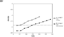
- FIG. 2 is a diagram showing the relationship between the ratio ts/tp and the ratio ⁇ ts/ ⁇ tp of the first resonator and the second resonator according to the first embodiment of the present invention.
- FIG. 3 shows an example of the relationship between the thickness deviation amount ⁇ tp of the piezoelectric layer and the trimming amount difference ⁇ ts between the first dielectric film and the second dielectric film in the first embodiment of the present invention. It is a diagram.
- FIG. 1 is a front cross-sectional view of an elastic wave device according to a first embodiment of the invention.
- FIG. 2 is a diagram showing the relationship between the ratio ts/tp and the ratio ⁇ ts/ ⁇ tp of the first resonator and the second resonator according to the first embodiment of the present invention.
- FIG. 3 shows an example of the relationship between the thickness deviation amount ⁇ tp of the pie
- FIG. 4 is a diagram showing the relationship between the thickness deviation amount ⁇ tp of the piezoelectric layer and the trimming amount difference ⁇ ts between the first dielectric film and the second dielectric film in the comparative example.
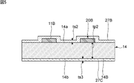
- FIG. 5 is a schematic front cross-sectional view showing the vicinity of a pair of electrode fingers of a second resonator according to a second embodiment of the present invention.
- FIG. 6 is a schematic front cross-sectional view showing the vicinity of a pair of electrode fingers of the first resonator according to the third embodiment of the present invention.
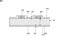
- FIG. 7 is a schematic front cross-sectional view showing the vicinity of a pair of electrode fingers of the second resonator according to the third embodiment of the present invention.
- FIG. 5 is a schematic front cross-sectional view showing the vicinity of a pair of electrode fingers of a second resonator according to a second embodiment of the present invention.
- FIG. 8 is a front cross-sectional view of an elastic wave device according to a fourth embodiment of the invention.
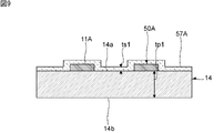
- FIG. 9 is a schematic front sectional view showing the vicinity of a pair of electrode fingers of the first resonator in the reference example.
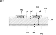
- FIG. 10 is a schematic front cross-sectional view showing the vicinity of a pair of electrode fingers of the second resonator in the reference example.
- FIG. 11 is a diagram showing the relationship between the ratio ts/tp and the ratio ⁇ ts/ ⁇ tp of the first resonator and the second resonator in the reference example.
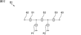
- FIG. 12 is a circuit diagram of an acoustic wave device according to the fifth embodiment.
- FIG. 12 is a circuit diagram of an acoustic wave device according to the fifth embodiment.
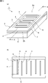
- FIG. 13(a) is a schematic perspective view showing the external appearance of an elastic wave device that utilizes thickness-shear mode bulk waves
- FIG. 13(b) is a plan view showing an electrode structure on a piezoelectric layer
- FIG. 14 is a cross-sectional view of a portion taken along line AA in FIG. 13(a).
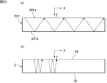
- FIG. 15(a) is a schematic front cross-sectional view for explaining a Lamb wave propagating through a piezoelectric film of an acoustic wave device
- FIG. 15(b) is a thickness shear propagating
- FIG. 2 is a schematic front cross-sectional view for explaining bulk waves in a mode;
- FIG. 16 is a diagram showing amplitude directions of bulk waves in the thickness shear mode.
- FIG. 17 is a diagram showing resonance characteristics of an elastic wave device that utilizes bulk waves in a thickness-shear mode.
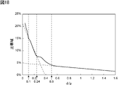
- FIG. 18 is a diagram showing the relationship between d/p and the fractional bandwidth of the resonator, where p is the center-to-center distance between adjacent electrodes and d is the thickness of the piezoelectric layer.
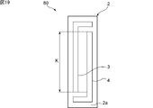
- FIG. 19 is a plan view of an elastic wave device that utilizes thickness shear mode bulk waves.
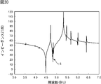
- FIG. 20 is a diagram showing the resonance characteristics of the elastic wave device of the reference example in which spurious appears.
- FIG. 21 is a diagram showing the relationship between the fractional bandwidth and the amount of phase rotation of the spurious impedance normalized by 180 degrees as the magnitude of the spurious.
- FIG. 22 is a diagram showing the relationship between d/2p and the metallization ratio MR.
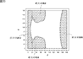
- FIG. 23 is a diagram showing a map of fractional bandwidth with respect to Euler angles (0°, ⁇ , ⁇ ) of LiNbO 3 when d/p is brought infinitely close to 0.
- FIG. 23 is a diagram showing a map of fractional bandwidth with respect to Euler angles (0°, ⁇ , ⁇ ) of LiNbO 3 when d/p is brought infinitely close to 0.
- FIG. 1 is a front cross-sectional view of an elastic wave device according to the first embodiment of the present invention.
- the elastic wave device 10 has a piezoelectric substrate 12 .
- a first resonator 10A and a second resonator 10B are formed on the piezoelectric substrate 12 .
- Both the first resonator 10A and the second resonator 10B are elastic wave resonators.
- both the first resonator 10A and the second resonator 10B are configured to be able to use bulk waves in a thickness-slip mode such as a first-order thickness-slip mode.
- the elastic wave device 10 can be used, for example, as part of a filter device.
- the resonance frequency of the first resonator 10A is higher than the resonance frequency of the second resonator 10B.
- the first resonator 10A is a series arm resonator.
- the second resonator 10B is a parallel arm resonator.
- the number of resonators in elastic wave device 10 is not limited to two, and may be three or more.
- the elastic wave device 10 itself may be a filter device.
- the piezoelectric substrate 12 has a support member 13 and a piezoelectric layer 14 .
- the support member 13 includes a support substrate 16 and an insulating layer 15 .
- An insulating layer 15 is provided on the support substrate 16 .
- a piezoelectric layer 14 is provided on the insulating layer 15 .
- the support member 13 may be composed of only the support substrate 16 .
- the piezoelectric layer 14 is a lithium niobate layer in this embodiment. More specifically, the piezoelectric layer 14 is a Z-cut LiNbO 3 layer. However, the piezoelectric layer 14 may also be, for example, a lithium tantalate layer, such as a LiTaO 3 layer.
- the supporting member 13 of the piezoelectric substrate 12 is provided with a hollow portion 13a and a hollow portion 13b. More specifically, the hollow portions 13 a and 13 b are formed by hollow portions provided in the insulating layer 15 portion of the piezoelectric substrate 12 .
- the cavity portion 13a and the cavity portion 13b may be provided in the insulating layer 15 and the support substrate 16, or may be provided in the support substrate 16 only.
- the hollow portion 13 a and the hollow portion 13 b may be configured by through holes provided in the support member 13 . It is sufficient that the support member 13 is provided with at least one cavity.
- the piezoelectric layer 14 has a first main surface 14a and a second main surface 14b.
- the first main surface 14a and the second main surface 14b face each other.
- the second principal surface 14b is located on the support member 13 side.
- a first IDT electrode 11A is provided on the first main surface 14a.
- a first resonator 10A is provided.
- a second IDT electrode 11B is provided on the first main surface 14a. This constitutes the second resonator 10B.
- the first resonator 10A and the second resonator 10B share the piezoelectric layer 14.
- the first IDT electrode 11A and the second IDT electrode 11B each have a plurality of electrode fingers.
- the first IDT electrode 11A is the first functional electrode of the invention.
- the second IDT electrode 11B is the second functional electrode in the present invention.
- the electrode finger is an electrode in the present invention.
- the piezoelectric layer 14 includes a first resonator portion 14A and a second resonator portion 14B.
- the first resonator portion 14A is a portion of the piezoelectric layer 14 where the first resonator 10A is formed. More specifically, as indicated by an arrow E1 in FIG. 1, the first resonator portion 14A is the portion of the piezoelectric layer 14 where the first IDT electrode 11A is provided.
- the second resonator portion 14B is the portion of the piezoelectric layer 14 where the second resonator 10B is formed. More specifically, the second resonator portion 14B is a portion of the piezoelectric layer 14 where the second IDT electrode 11B is provided, as indicated by arrow E2 in FIG.
- the direction in which adjacent electrode fingers face each other is defined as the electrode finger facing direction.
- the range in the electrode-finger facing direction of the first resonator portion 14A extends from the portion of the first IDT electrode 11A where the electrode finger at one end in the electrode-finger facing direction is provided to the electrode finger at the other end. range up to the part where Similarly, the range in the electrode finger facing direction of the second resonator portion 14B extends from the portion where the electrode finger at one end in the electrode finger facing direction of the second IDT electrode 11B is provided to the electrode finger at the other end in the electrode finger facing direction. is the range up to the part where is provided.
- first IDT electrode 11A overlaps the hollow portion 13a in plan view.
- second IDT electrode 11B overlaps the cavity 13b.
- first IDT electrode 11A and the second IDT electrode 11B may overlap the same cavity in plan view.
- planar view means viewing from a direction corresponding to the upper side in FIG. In FIG. 1, for example, between the support substrate 16 and the piezoelectric layer 14, the piezoelectric layer 14 side is the upper side.
- the first resonator 10A has a first dielectric film 17A.
- the first dielectric film 17A is provided on the first major surface 14a of the piezoelectric layer 14 so as to cover the first IDT electrode 11A.
- the second resonator 10B has a second dielectric film 17B and a third dielectric film 17C.
- the second dielectric film 17B is provided on the first main surface 14a of the piezoelectric layer 14 so as to cover the second IDT electrode 11B.
- the first dielectric film 17A and the second dielectric film 17B are integrally provided. More specifically, a dielectric film is provided to cover the first IDT electrode 11A and the second IDT electrode 11B. A portion of the dielectric film that overlaps the first resonator portion 14A of the piezoelectric layer 14 in plan view is the first dielectric film 17A. A portion of the dielectric film overlapping the second resonator portion 14B in plan view is the second dielectric film 17B.
- the first dielectric film 17A and the second dielectric film 17B may be provided separately from each other.
- the third dielectric film 17C is provided on the second main surface 14b of the piezoelectric layer 14 so as to overlap the second IDT electrode 11B in plan view. Therefore, the third dielectric film 17C is provided on a portion of the second principal surface 14b located at the second resonator portion 14B. More specifically, the third dielectric film 17C is located inside the cavity 13b. In this embodiment, the third dielectric film 17C is provided integrally with the insulating layer 15. As shown in FIG. However, the third dielectric film 17C may be provided separately from the insulating layer 15 .
- the first dielectric film 17A, the second dielectric film 17B and the third dielectric film 17C are frequency adjustment films. By trimming the first dielectric film 17A and adjusting the thickness of the first dielectric film 17A, the frequency of the first resonator 10A can be adjusted. Similarly, by trimming the second dielectric film 17B and adjusting the total thickness of the second dielectric film 17B and the third dielectric film 17C, the frequency of the second resonator 10B is adjusted. can do.
- the first dielectric film 17A, the second dielectric film 17B, and the third dielectric film 17C may be collectively referred to as frequency adjustment films.
- the first dielectric film 17A, the second dielectric film 17B and the third dielectric film 17C are made of silicon oxide. More specifically, each dielectric film is made of SiO2 .
- the materials for the first dielectric film 17A, the second dielectric film 17B, and the third dielectric film 17C are not limited to those described above, and silicon nitride, for example, can also be used.
- the term "a certain member is made of a certain material" includes the case where a minute amount of impurity is included to such an extent that the electrical characteristics of the acoustic wave device are not significantly degraded.
- the thickness of the first resonator portion 14A of the piezoelectric layer 14 is tp1
- the thickness of the second resonator portion 14B is tp2.
- the thickness tp1 and the thickness tp2 are collectively referred to as the thickness tp of the resonator portion.
- ts1 be the thickness of the first dielectric film 17A
- ts2 be the thickness of the second dielectric film 17B
- ts3 be the thickness of the third dielectric film 17C.
- the thickness ts1, the thickness ts2, and the thickness ts3 are collectively referred to as the thickness ts of the dielectric film.
- ⁇ tp be the amount of deviation in the thickness of the piezoelectric layer 14
- ⁇ ts be the difference in the amount of trimming of the first dielectric film 17A, the second dielectric film 17B, or the third dielectric film 17C.
- the first dielectric film 17A and the second dielectric film 17B are trimmed in adjusting the frequency.
- the deviation amount ⁇ tp is the deviation amount of the thickness of the piezoelectric layer 14 from the target value.
- the trimming amount difference ⁇ ts is the difference between the amount of trimming when the thickness of the piezoelectric layer 14 is the target value and the amount of trimming when the thickness of the piezoelectric layer 14 deviates from the target value.
- the ratio of the trimming amount difference ⁇ ts to the shift amount ⁇ tp is ⁇ ts/ ⁇ tp.
- the thickness ts1 of the first dielectric film 17A is the thickness of the first main surface 14a of the piezoelectric layer 14 and the thickness of the first dielectric film 17A in the portion where the first IDT electrode 11A is not provided. is the distance between the surface of The thickness ts2 of the second dielectric film 17B is between the first main surface 14a of the piezoelectric layer 14 and the surface of the second dielectric film 17B in the portion where the second IDT electrode 11B is not provided. distance.
- the thickness ts3 of the third dielectric film 17C is the distance between the second main surface 14b of the piezoelectric layer 14 and the surface of the third dielectric film 17C. Note that the thickness ts3 may be the above-mentioned distance in the portion overlapping with the second IDT electrode 11B in plan view.
- a feature of this embodiment is that the first resonator 10A has a first dielectric film 17A, and the second resonator 10B has both a second dielectric film 17B and a third dielectric film 17C. and ts1/tp1 ⁇ (ts2+ts3)/tp2.
- variations in the trimming amount difference ⁇ ts of the frequency adjustment film can be suppressed between the first resonator 10A and the second resonator 10B, and variations in frequency can be suppressed. Details of this are described below.
- the resonance frequencies of the first resonator 10A and the second resonator 10B are different from each other. Therefore, the thicknesses of the frequency adjustment films formed in the first resonator 10A and the second resonator 10B are also different from each other. Therefore, if the elastic wave device 10 has a conventional configuration, the difference in the amount of trimming required when the thickness of the piezoelectric layer 14 deviates from the target value is between the first resonator 10A and the second resonator 10B. ⁇ ts will be different from each other.
- the ratio ⁇ ts/ ⁇ tp of the trimming amount difference ⁇ ts to the deviation amount ⁇ tp of the thickness of the piezoelectric layer 14 from the target value differs between the acoustic wave resonators.
- the amount of trimming required for each acoustic wave resonator includes the trimming amount difference ⁇ ts that is different from each other, a frequency deviation accumulates for each acoustic wave resonator due to errors and the like. Become.
- the inventors of the present application have found that by setting ts1/tp1 ⁇ (ts2+ts3)/tp2, the ratios ⁇ ts/ ⁇ tp between the acoustic wave resonators can be made closer to each other, and the trimming amount difference ⁇ ts can be made closer to each other. I found that I could get closer.
- FIG. 2 is a diagram showing the relationship between the ratio ts/tp and the ratio ⁇ ts/ ⁇ tp of the first resonator and the second resonator in the first embodiment.
- the relationships between the ratio ts/tp and the ratio ⁇ ts/ ⁇ tp are different between the first resonator 10A and the second resonator 10B.
- the ratio ⁇ ts/ ⁇ tp in the first resonator 10A is the same as the ratio ⁇ ts/ ⁇ tp in the second resonator 10B.
- both ratios ⁇ ts/ ⁇ tp can be made the same.
- the frequency adjustment film of the first resonator 10A is the first dielectric film 17A.
- the thickness ts of the first resonator 10A is ts1, and the thickness tp is tp1.
- the frequency adjustment films of the second resonator 10B are the second dielectric film 17B and the third dielectric film 17C.
- the thickness ts of the second resonator 10B is ts2+ts3, and the thickness tp is tp2. Therefore, by setting ts1/tp1 ⁇ (ts2+ts3)/tp2, both ratios ⁇ ts/ ⁇ tp can be made the same.
- the reason why the first resonator 10A and the second resonator 10B have different relationships between the ratio ts/tp and the ratio ⁇ ts/ ⁇ tp is that the positions of the frequency adjustment films are different.
- the frequency adjustment film of the first resonator 10A is provided on one main surface of the piezoelectric layer 14 .
- the frequency adjustment films of the second resonator 10B are provided on both main surfaces of the piezoelectric layer 14.
- the first resonator 10A and the second resonator 10B share the piezoelectric layer 14.
- the amount of deviation ⁇ tp in the thickness of the piezoelectric layer 14 is also the same between the resonator portions. In this case, by setting ts1/tp1 ⁇ (ts2+ts3)/tp2 and making both ratios .DELTA.ts/.DELTA.tp the same, both trimming amount differences .DELTA.ts can be made the same.
- the frequency adjustment films in the first resonator 10A and the second resonator 10B at the same time.
- the accumulation of errors for each trimming can be suppressed, and the frequency shift for each elastic wave resonator can be effectively suppressed. Therefore, the elastic wave device 10 as a whole can effectively suppress variations in frequency.
- the second dielectric film 17B and the third dielectric film 17C are made of the same kind of dielectric.
- the relationships between the ratio ts/tp and the ratio .DELTA.ts/.DELTA.tp in the first resonator 10A and the second resonator 10B can be made different from each other more reliably, as shown in FIG. Therefore, ⁇ ts/ ⁇ tp can be more reliably made the same between the elastic wave resonators.
- the ratio ⁇ ts/ ⁇ tp can be the same between the first resonator 10A and the second resonator 10B.
- the ratio ⁇ ts/ ⁇ tp may not be completely the same between the elastic wave resonators.
- the thickness tp of the first resonator portion 14A and the second resonator portion 14B of the piezoelectric layer 14 in this example, and the first dielectric film 17A, the second dielectric film 17B and the third dielectric film 17C The thickness ts of is as follows.
- the piezoelectric layer 14 consists of Z-cut LiNbO 3 .
- the first dielectric film 17A, the second dielectric film 17B and the third dielectric film 17C are all made of SiO2 .
- Thickness tp1 of the first resonator portion 370 nm Thickness tp2 of the second resonator portion; 370 nm Thickness ts1 of the first dielectric film; 48 nm Thickness ts2 of the second dielectric film; 48 nm Thickness ts3 of the third dielectric film; 110 nm
- FIG. 3 is a diagram showing an example of the relationship between the thickness deviation amount ⁇ tp of the piezoelectric layer and the trimming amount difference ⁇ ts between the first dielectric film and the second dielectric film in the first embodiment. be.
- ⁇ ts/ ⁇ tp are not completely the same between the first resonator 10A and the second resonator 10B. Even in this case, for example, when ⁇ tp is within ⁇ 10 nm, the difference in trimming amount difference ⁇ ts between the first resonator 10A and the second resonator 10B is 1 nm or less. In this way, when the trimming amount differences ⁇ ts can be made close to each other, if the trimming amounts themselves are also close to each other, the trimming of the frequency adjustment films in the first resonator 10A and the second resonator 10B can be performed at the same time. preferably.
- the ratio ⁇ ts/ ⁇ tp differs greatly between elastic wave resonators.
- the comparative example differs from the first embodiment in that the frequency adjustment film of the second resonator is only the second dielectric film.
- the third dielectric film is not provided on the second main surface of the piezoelectric layer.
- Thickness tp1 of the first resonator portion 373 nm Thickness tp2 of the second resonator portion; 373 nm Thickness ts1 of the first dielectric film; 43 nm Thickness ts2 of the second dielectric film; 133 nm
- FIG. 4 is a diagram showing the relationship between the thickness deviation amount ⁇ tp of the piezoelectric layer and the trimming amount difference ⁇ ts between the first dielectric film and the second dielectric film in the comparative example.
- the ratio ⁇ ts/ ⁇ tp is significantly different between the first resonator and the second resonator. Specifically, the ratio ⁇ ts/ ⁇ tp in the first resonator is ⁇ 1.08, and the ratio ⁇ ts/ ⁇ tp in the second resonator is ⁇ 1.79.
- the desired frequencies are different from each other, so the thicknesses of the first dielectric film and the second dielectric film when formed are different from each other. Therefore, as described above, when the thickness of the piezoelectric layer 14 deviates from the target value, the trimming amount differences ⁇ ts differ greatly from each other. Therefore, in the comparative example, if the frequency adjustment films of the first resonator and the second resonator are trimmed at the same time, the first resonator or the second resonator deviates from the desired frequency. There is a risk. On the other hand, even if trimming is performed for each acoustic wave resonator, there is a possibility that trimming errors will accumulate.
- the trimming amount difference ⁇ ts in the first resonator 10A and the second resonator 10B can be made close to each other.
- the elastic wave device 10 as a whole can suppress variations in frequency.
- the dielectric film is not provided on the portion of the second main surface 14b of the piezoelectric layer 14 located at the first resonator portion 14A.
- a thin dielectric film may be provided to the extent that the electrical characteristics of the acoustic wave device 10 are not greatly affected.
- the elastic wave device 10 does not necessarily have to have the support member 13 . It is sufficient that the first resonator 10A and the second resonator 10B are configured to be able to use thickness-shear mode bulk waves or the like.
- the second dielectric film 17B and the third dielectric film 17C are made of the same kind of dielectric.
- the second dielectric film 17B and the third dielectric film 17C may be made of different kinds of dielectrics.
- FIG. 5 is a schematic front cross-sectional view showing the vicinity of a pair of electrode fingers of the second resonator according to the second embodiment.
- This embodiment differs from the first embodiment in that the second dielectric film 27B and the third dielectric film 27C in the second resonator 20B are made of different types of dielectrics. Except for the above points, the elastic wave device of this embodiment has the same configuration as the elastic wave device 10 of the first embodiment. In addition, in this embodiment, the reference numerals of the configuration in the first embodiment shown in FIG. 1 are used for the reference numerals other than the configuration of the second resonator 20B.
- the second dielectric film 27B and the third dielectric film 27C have the same thickness.
- a state is a preferred state. More specifically, the preferable state is a state in which the mass per unit area of the second dielectric film 27B and the mass per unit area of the third dielectric film 27C are the same.
- the thicknesses of the second dielectric film 27B and the third dielectric film 27C are adjusted according to the density. Thereby, the mass per unit area of the second dielectric film 27B and the mass per unit area of the third dielectric film 27C can be brought close to each other.
- the dielectric film with the higher density is preferably thinner than the dielectric film with the lower density.
- the mass per unit area of the second dielectric film 27B and the mass per unit area of the third dielectric film 27C can easily be made the same.
- the thickness of the second dielectric film 27B and the third dielectric film 27C may be adjusted according to the acoustic impedance.
- the first dielectric film 17A in the first resonator 10A and the second dielectric film 27B in the second resonator 20B are made of the same kind of dielectric.
- the first dielectric film 17A and the second dielectric film 27B may be made of different kinds of dielectrics.
- FIG. 6 is a schematic front sectional view showing the vicinity of a pair of electrode fingers of the first resonator according to the third embodiment.
- FIG. 7 is a schematic front cross-sectional view showing the vicinity of a pair of electrode fingers of the second resonator according to the third embodiment.
- this embodiment differs from the first embodiment in that tp1 ⁇ tp2. Except for the above points, the elastic wave device of this embodiment has the same configuration as the elastic wave device 10 of the first embodiment.
- the piezoelectric layer 34 is provided with a stepped portion so that the thickness tp1 of the first resonator portion 34A and the thickness tp2 of the second resonator portion 34B are different from each other.
- the stepped portion may be provided on at least one of the first main surface 34a side and the second main surface 34b side.
- FIG. 8 is a front cross-sectional view of an elastic wave device according to a fourth embodiment.
- This embodiment differs from the first embodiment in that the first IDT electrode 11A, the second IDT electrode 11B and the first dielectric film 17A are provided on the second main surface 14b of the piezoelectric layer 14. Different from the form.
- This embodiment is different from the first embodiment in that the third dielectric film 17C covers the second IDT electrode 11B and the second dielectric film 17B does not cover the second IDT electrode 11B. Different from the form.
- this embodiment differs from the first embodiment in the configuration of the support member 43 . Except for the above points, the elastic wave device of this embodiment has the same configuration as the elastic wave device 10 of the first embodiment.
- the support member 43 has a support substrate 46 and an insulating layer 45 .
- the support substrate 46 is provided with two through holes.
- An insulating layer 45 is provided on the support substrate 46 so as to close the two through holes. Thereby, a cavity portion 43a and a cavity portion 43b are formed.
- a piezoelectric layer 14 is provided on the insulating layer 45 .
- the first dielectric film 17A and the third dielectric film 17C are provided integrally with the insulating layer 45 .
- the thickness ts1 of the first dielectric film 17A is the thickness of the second main surface 14b of the piezoelectric layer 14 and the thickness of the first dielectric film 17A in the portion where the first IDT electrode 11A is not provided. is the distance between the surface of
- the thickness ts2 of the second dielectric film 17B is the distance between the first main surface 14a of the piezoelectric layer 14 and the surface of the second dielectric film 17B.
- the thickness ts3 of the third dielectric film 17C is between the second main surface 14b of the piezoelectric layer 14 and the surface of the third dielectric film 17C in the portion where the second IDT electrode 11B is not provided. distance.
- the first dielectric film 17A and the second dielectric film 17B are trimmed in adjusting the frequency.
- the first dielectric film 17A and the third dielectric film 17C are trimmed in adjusting the frequency.
- the cavity 43a and the cavity 43b are formed by through-holes, the first dielectric film 17A and the third dielectric film 17C can be suitably trimmed.
- the inventor of the present application can make ⁇ ts/ ⁇ tp closer to each other between the first resonator and the second resonator even when ts1/tp1 ⁇ (ts2+ts3)/tp2 is not satisfied. I found that there is a case. Specifically, even when the dielectric films to be trimmed are made of different types of dielectrics and ts1/tp1>(ts2+ts3)/tp2, ⁇ ts/ ⁇ tp between the elastic wave resonators is may be brought closer together. This example is shown below as a reference example.
- FIG. 9 is a schematic front sectional view showing the vicinity of a pair of electrode fingers of the first resonator in the reference example.
- FIG. 10 is a schematic front cross-sectional view showing the vicinity of a pair of electrode fingers of the second resonator in the reference example.
- the first dielectric film 57A in the first resonator 50A and the second dielectric film 17B in the second resonator 50B are of different types. It differs from the first embodiment in that it is made of a dielectric.
- the reference example also differs from the first embodiment in that ts1/tp1>(ts2+ts3)/tp2. Except for the above points, the elastic wave device of the reference example has the same configuration as the elastic wave device 10 of the first embodiment.
- the first dielectric film 57A in the reference example is made of SiN.
- the second dielectric film 17B and the third dielectric film 17C are made of SiO2 .
- FIG. 11 is a diagram showing the relationship between the ratio ts/tp and the ratio ⁇ ts/ ⁇ tp of the first resonator and the second resonator in the reference example.
- the magnitude relationship of the ratio ⁇ ts/ ⁇ tp between the first resonator 50A and the second resonator 50B is reversed with the value 0.045 of the ratio ts/tp as the boundary.
- the ratio ⁇ ts/ ⁇ tp in the first resonator 50A is the same as the ratio ⁇ ts/ ⁇ tp in the second resonator 50B.
- the acoustic impedance of the second dielectric film 17B is higher than the acoustic impedance of the first dielectric film 57A.
- the resonance frequency of the first resonator may be lower than the second resonance frequency.
- the elastic wave device according to the present invention may be a filter device.
- An example of an acoustic wave device as a filter device is shown below.
- FIG. 12 is a circuit diagram of an acoustic wave device according to the fifth embodiment.
- the elastic wave device 61 is a ladder filter.
- the elastic wave device 61 has a first signal terminal 62, a second signal terminal 63, a plurality of series arm resonators and a plurality of parallel arm resonators.
- the first signal terminal 62 and the second signal terminal 63 may be configured as electrode pads, or may be configured as wiring, for example.
- the first signal terminal 62 is an antenna terminal.
- An antenna terminal is connected to the antenna.
- the multiple series arm resonators of the elastic wave device 61 are specifically a series arm resonator S1, a series arm resonator S2, and a series arm resonator S3.
- the plurality of parallel arm resonators are specifically a parallel arm resonator P1 and a parallel arm resonator P2.
- the series arm resonator S1 is the first resonator in the present invention.
- the parallel arm resonator P1 is the second resonator in the present invention.
- the series arm resonator S1 is connected between the connection point between the series arm resonators S1 and S2 and the ground potential.
- a parallel arm resonator P2 is connected between the connection point between the series arm resonators S2 and S3 and the ground potential.
- the elastic wave device 61 may have a first resonator as a series arm resonator and a second resonator as a parallel arm resonator.
- the elastic wave device 61 has a first resonator and a second resonator in the present invention. Therefore, similarly to the first embodiment and the like, it is possible to suppress variation in difference in trimming amount of the frequency adjustment film between elastic wave resonators, and to suppress variation in frequency.
- the elastic wave device 61 may have a plurality of first resonators of the present invention or a plurality of second resonators of the present invention.
- at least one of the plurality of series arm resonators may be the first resonator
- at least one of the plurality of parallel arm resonators may be the second resonator.
- the elastic wave device of the present invention When the elastic wave device of the present invention is a filter device, the elastic wave device has a first resonator as a parallel arm resonator and a second resonator as a series arm resonator.
- the elastic wave device has a first resonator as a parallel arm resonator and a second resonator as a series arm resonator.
- at least one of the parallel arm resonators P1 and P2 as the plurality of parallel arm resonators should be the first resonator.
- At least one of the series arm resonator S1, the series arm resonator S2, and the series arm resonator S3 as the plurality of series arm resonators may be the second resonator.
- the details of the thickness slip mode will be explained below.
- the first IDT electrode 11A and the second IDT electrode 11B have the structure of an IDT electrode, which will be described later.
- the supporting member in the following examples corresponds to the supporting substrate in the present invention.
- FIG. 13(a) is a schematic perspective view showing the external appearance of an acoustic wave device that utilizes a thickness shear mode bulk wave
- FIG. 13(b) is a plan view showing an electrode structure on a piezoelectric layer
- FIG. 14 is a cross-sectional view of a portion taken along line AA in FIG. 13(a).
- the acoustic wave device 1 has a piezoelectric layer 2 made of LiNbO 3 .
- the piezoelectric layer 2 may consist of LiTaO 3 .
- the cut angle of LiNbO 3 and LiTaO 3 is Z-cut, but may be rotational Y-cut or X-cut.
- the thickness of the piezoelectric layer 2 is not particularly limited, it is preferably 40 nm or more and 1000 nm or less, more preferably 50 nm or more and 1000 nm or less, in order to effectively excite the thickness-shear mode.
- the piezoelectric layer 2 has first and second major surfaces 2a and 2b facing each other. Electrodes 3 and 4 are provided on the first main surface 2a.
- the electrode 3 is an example of the "first electrode” and the electrode 4 is an example of the "second electrode".
- 13(a) and 13(b) a plurality of electrodes 3 are connected to a first busbar 5.
- a plurality of electrodes 4 are connected to a second bus bar 6 .
- the plurality of electrodes 3 and the plurality of electrodes 4 are interleaved with each other.
- Electrodes 3 and 4 have a rectangular shape and a length direction.
- the electrode 3 and the adjacent electrode 4 face each other in a direction perpendicular to the length direction. Both the length direction of the electrodes 3 and 4 and the direction orthogonal to the length direction of the electrodes 3 and 4 are directions crossing the thickness direction of the piezoelectric layer 2 .
- the electrode 3 and the adjacent electrode 4 face each other in the direction crossing the thickness direction of the piezoelectric layer 2 .
- the length direction of the electrodes 3 and 4 may be interchanged with the direction orthogonal to the length direction of the electrodes 3 and 4 shown in FIGS. 13(a) and 13(b). That is, in FIGS. 13A and 13B, the electrodes 3 and 4 may extend in the direction in which the first busbar 5 and the second busbar 6 extend. In that case, the first busbar 5 and the second busbar 6 extend in the direction in which the electrodes 3 and 4 extend in FIGS. 13(a) and 13(b).
- a plurality of pairs of structures in which an electrode 3 connected to one potential and an electrode 4 connected to the other potential are adjacent to each other are provided in a direction perpendicular to the length direction of the electrodes 3 and 4.
- the electrodes 3 and 4 are adjacent to each other, it does not mean that the electrodes 3 and 4 are arranged so as to be in direct contact with each other, but that the electrodes 3 and 4 are arranged with a gap therebetween. point to When the electrodes 3 and 4 are adjacent to each other, no electrodes connected to the hot electrode or the ground electrode, including the other electrodes 3 and 4, are arranged between the electrodes 3 and 4.
- the logarithms need not be integer pairs, but may be 1.5 pairs, 2.5 pairs, or the like.
- the center-to-center distance or pitch between the electrodes 3 and 4 is preferably in the range of 1 ⁇ m or more and 10 ⁇ m or less.
- the width of the electrodes 3 and 4, that is, the dimension of the electrodes 3 and 4 in the facing direction is preferably in the range of 50 nm or more and 1000 nm or less, more preferably in the range of 150 nm or more and 1000 nm or less.
- the center-to-center distance between the electrodes 3 and 4 means the distance between the center of the dimension (width dimension) of the electrode 3 in the direction orthogonal to the length direction of the electrode 3 and the distance between the center of the electrode 4 in the direction orthogonal to the length direction of the electrode 4. It is the distance connecting the center of the dimension (width dimension) of
- the direction perpendicular to the length direction of the electrodes 3 and 4 is the direction perpendicular to the polarization direction of the piezoelectric layer 2 .
- “perpendicular” is not limited to being strictly perpendicular, but is substantially perpendicular (the angle formed by the direction perpendicular to the length direction of the electrodes 3 and 4 and the polarization direction is, for example, 90° ⁇ 10°). within the range).
- a supporting member 8 is laminated on the second main surface 2b side of the piezoelectric layer 2 with an insulating layer 7 interposed therebetween.
- the insulating layer 7 and the support member 8 have a frame-like shape and, as shown in FIG. 14, have through holes 7a and 8a.
- a cavity 9 is thereby formed.
- the cavity 9 is provided so as not to disturb the vibration of the excitation region C of the piezoelectric layer 2 . Therefore, the support member 8 is laminated on the second main surface 2b with the insulating layer 7 interposed therebetween at a position not overlapping the portion where at least one pair of electrodes 3 and 4 are provided. Note that the insulating layer 7 may not be provided. Therefore, the support member 8 can be directly or indirectly laminated to the second main surface 2b of the piezoelectric layer 2 .
- the insulating layer 7 is made of silicon oxide. However, in addition to silicon oxide, suitable insulating materials such as silicon oxynitride and alumina can be used.
- the support member 8 is made of Si. The plane orientation of the surface of Si on the piezoelectric layer 2 side may be (100), (110), or (111). It is desirable that the Si constituting the support member 8 has a high resistivity of 4 k ⁇ cm or more. However, the support member 8 can also be constructed using an appropriate insulating material or semiconductor material.
- Materials for the support member 8 include, for example, aluminum oxide, lithium tantalate, lithium niobate, piezoelectric materials such as crystal, alumina, magnesia, sapphire, silicon nitride, aluminum nitride, silicon carbide, zirconia, cordierite, mullite, and steer.
- Various ceramics such as tight and forsterite, dielectrics such as diamond and glass, and semiconductors such as gallium nitride can be used.
- the plurality of electrodes 3, 4 and the first and second bus bars 5, 6 are made of appropriate metals or alloys such as Al, AlCu alloys.
- the electrodes 3 and 4 and the first and second bus bars 5 and 6 have a structure in which an Al film is laminated on a Ti film. Note that an adhesion layer other than the Ti film may be used.
- d/p is 0.0, where d is the thickness of the piezoelectric layer 2 and p is the center-to-center distance between any one of the pairs of electrodes 3 and 4 adjacent to each other. 5 or less. Therefore, the thickness-shear mode bulk wave is effectively excited, and good resonance characteristics can be obtained. More preferably, d/p is 0.24 or less, in which case even better resonance characteristics can be obtained.
- the elastic wave device 1 Since the elastic wave device 1 has the above configuration, even if the logarithm of the electrodes 3 and 4 is reduced in an attempt to reduce the size, the Q value is unlikely to decrease. This is because the propagation loss is small even if the number of electrode fingers in the reflectors on both sides is reduced. Moreover, the fact that the number of electrode fingers can be reduced is due to the fact that bulk waves in the thickness-shear mode are used. The difference between the Lamb wave used in the elastic wave device and the bulk wave in the thickness shear mode will be described with reference to FIGS. 15(a) and 15(b).
- FIG. 15(a) is a schematic front cross-sectional view for explaining a Lamb wave propagating through a piezoelectric film of an acoustic wave device as described in Japanese Unexamined Patent Publication No. 2012-257019.
- waves propagate through the piezoelectric film 201 as indicated by arrows.
- the first main surface 201a and the second main surface 201b face each other, and the thickness direction connecting the first main surface 201a and the second main surface 201b is the Z direction. is.
- the X direction is the direction in which the electrode fingers of the IDT electrodes are arranged.
- the Lamb wave propagates in the X direction as shown.
- the wave is generated on the first principal surface 2a and the second principal surface of the piezoelectric layer 2. 2b, ie, the Z direction, and resonates. That is, the X-direction component of the wave is significantly smaller than the Z-direction component. Further, since resonance characteristics are obtained by propagating waves in the Z direction, propagation loss is unlikely to occur even if the number of electrode fingers of the reflector is reduced. Furthermore, even if the number of electrode pairs consisting of the electrodes 3 and 4 is reduced in an attempt to promote miniaturization, the Q value is unlikely to decrease.
- FIG. 16 schematically shows a bulk wave when a voltage is applied between the electrodes 3 and 4 so that the potential of the electrode 4 is higher than that of the electrode 3 .
- the first region 451 is a region of the excitation region C between the first main surface 2a and a virtual plane VP1 that is perpendicular to the thickness direction of the piezoelectric layer 2 and bisects the piezoelectric layer 2 .
- the second region 452 is a region of the excitation region C between the virtual plane VP1 and the second main surface 2b.
- the acoustic wave device 1 at least one pair of electrodes consisting of the electrodes 3 and 4 is arranged.
- the number of electrode pairs need not be plural. That is, it is sufficient that at least one pair of electrodes is provided.
- the electrode 3 is an electrode connected to a hot potential
- the electrode 4 is an electrode connected to a ground potential.
- electrode 3 may also be connected to ground potential and electrode 4 to hot potential.
- at least one pair of electrodes is an electrode connected to a hot potential or an electrode connected to a ground potential, as described above, and no floating electrodes are provided.
- FIG. 17 is a diagram showing resonance characteristics of the elastic wave device shown in FIG.
- the design parameters of the elastic wave device 1 with this resonance characteristic are as follows.
- Insulating layer 7 Silicon oxide film with a thickness of 1 ⁇ m.
- Support member 8 Si.
- the length of the excitation region C is the dimension along the length direction of the electrodes 3 and 4 of the excitation region C.
- the inter-electrode distances of the electrode pairs consisting of the electrodes 3 and 4 are all the same in a plurality of pairs. That is, the electrodes 3 and 4 were arranged at equal pitches.
- d/p is more preferably 0.5 or less, as described above. is less than or equal to 0.24. This will be described with reference to FIG.
- FIG. 18 is a diagram showing the relationship between this d/p and the fractional bandwidth of the acoustic wave device as a resonator.
- the specific bandwidth when d/p>0.5, even if d/p is adjusted, the specific bandwidth is less than 5%.
- the specific bandwidth when d/p ⁇ 0.5, the specific bandwidth can be increased to 5% or more by changing d/p within that range. can be configured. Further, when d/p is 0.24 or less, the specific bandwidth can be increased to 7% or more.
- d/p when adjusting d/p within this range, a resonator with a wider specific band can be obtained, and a resonator with a higher coupling coefficient can be realized. Therefore, by setting d/p to 0.5 or less, it is possible to construct a resonator having a high coupling coefficient using the thickness-shear mode bulk wave.
- FIG. 19 is a plan view of an elastic wave device that utilizes thickness-shear mode bulk waves.
- elastic wave device 80 a pair of electrodes having electrode 3 and electrode 4 is provided on first main surface 2 a of piezoelectric layer 2 .
- K in FIG. 19 is the crossing width.
- the number of pairs of electrodes may be one. Even in this case, if d/p is 0.5 or less, bulk waves in the thickness-shear mode can be effectively excited.
- the adjacent excitation region C is an overlapping region when viewed in the direction in which any of the adjacent electrodes 3 and 4 are facing each other. It is desirable that the metallization ratio MR of the mating electrodes 3, 4 satisfy MR ⁇ 1.75(d/p)+0.075. In that case, spurious can be effectively reduced. This will be described with reference to FIGS. 20 and 21.
- FIG. FIG. 20 is a reference diagram showing an example of resonance characteristics of the acoustic wave device 1.
- the metallization ratio MR will be explained with reference to FIG. 13(b).
- the excitation region C is the portion surrounded by the dashed-dotted line.
- the excitation region C is a region in which the electrode 3 and the electrode 4 overlap each other when the electrodes 3 and 4 are viewed in a direction perpendicular to the length direction of the electrodes 3 and 4, that is, in a facing direction. 3 and an overlapping area between the electrodes 3 and 4 in the area between the electrodes 3 and 4 .
- the area of the electrodes 3 and 4 in the excitation region C with respect to the area of the excitation region C is the metallization ratio MR. That is, the metallization ratio MR is the ratio of the area of the metallization portion to the area of the excitation region C.
- MR may be the ratio of the metallization portion included in the entire excitation region to the total area of the excitation region.
- FIG. 21 is a diagram showing the relationship between the fractional bandwidth and the amount of phase rotation of the spurious impedance normalized by 180 degrees as the magnitude of the spurious when a large number of acoustic wave resonators are configured according to this embodiment. be.
- the ratio band was adjusted by changing the film thickness of the piezoelectric layer and the dimensions of the electrodes.
- FIG. 21 shows the results in the case of using a Z-cut LiNbO 3 piezoelectric layer, but the same tendency is obtained in the case of using piezoelectric layers with other cut angles.
- the spurious is as large as 1.0.
- the fractional band exceeds 0.17, that is, when it exceeds 17%, even if a large spurious with a spurious level of 1 or more changes the parameters constituting the fractional band, the passband appear within. That is, like the resonance characteristic shown in FIG. 20, a large spurious component indicated by arrow B appears within the band. Therefore, the specific bandwidth is preferably 17% or less. In this case, by adjusting the film thickness of the piezoelectric layer 2 and the dimensions of the electrodes 3 and 4, the spurious response can be reduced.
- FIG. 22 is a diagram showing the relationship between d/2p, metallization ratio MR, and fractional bandwidth.
- various elastic wave devices having different d/2p and MR were constructed, and the fractional bandwidth was measured.
- the hatched portion on the right side of the dashed line D in FIG. 22 is the area where the fractional bandwidth is 17% or less.
- FIG. 23 is a diagram showing a map of fractional bandwidth with respect to Euler angles (0°, ⁇ , ⁇ ) of LiNbO 3 when d/p is brought infinitely close to 0.
- FIG. The hatched portion in FIG. 23 is a region where a fractional bandwidth of at least 5% or more is obtained, and the range of the region is approximated by the following formulas (1), (2) and (3) ).
- Equation (1) (0° ⁇ 10°, 20° to 80°, 0° to 60° (1-( ⁇ -50) 2 /900) 1/2 ) or (0° ⁇ 10°, 20° to 80°, [180 °-60° (1-( ⁇ -50) 2 /900) 1/2 ] ⁇ 180°) Equation (2) (0° ⁇ 10°, [180°-30°(1-( ⁇ -90) 2 /8100) 1/2 ] ⁇ 180°, arbitrary ⁇ ) Equation (3)
- the fractional band can be sufficiently widened, which is preferable.
- the piezoelectric layer 2 is a lithium tantalate layer.
- d/p is 0.00 in each of the first resonator and the second resonator, as described above. It is preferably 5 or less, more preferably 0.24 or less. Thereby, even better resonance characteristics can be obtained. Furthermore, in the elastic wave devices of the first to fifth embodiments that utilize thickness-shear mode bulk waves, in each of the first resonator and the second resonator, MR ⁇ 1. 75(d/p)+0.075 is preferably satisfied. In this case, spurious can be suppressed more reliably.
- the first functional electrode and the second functional electrode in the elastic wave devices of the first to fifth embodiments that utilize thickness shear mode bulk waves are functional electrodes having a pair of electrodes shown in FIG. good too.
- the piezoelectric layer in the elastic wave devices of the first to fifth embodiments that utilize thickness shear mode bulk waves is preferably a lithium niobate layer or a lithium tantalate layer.
- the Euler angles ( ⁇ , ⁇ , ⁇ ) of lithium niobate or lithium tantalate constituting the piezoelectric layer are within the range of the above formula (1), formula (2), or formula (3). is preferred. In this case, the fractional bandwidth can be widened sufficiently.
Landscapes
- Physics & Mathematics (AREA)
- Acoustics & Sound (AREA)
- Chemical & Material Sciences (AREA)
- Crystallography & Structural Chemistry (AREA)
- Surface Acoustic Wave Elements And Circuit Networks Thereof (AREA)
- Piezo-Electric Or Mechanical Vibrators, Or Delay Or Filter Circuits (AREA)
Abstract
弾性波共振子間における、周波数調整膜のトリミングの量差分のばらつきを抑制することができ、周波数のばらつきを抑制することができる、弾性波装置を提供する。 本発明に係る弾性波装置10は、対向し合う第1の主面14a及び第2の主面14bを有する圧電層14を含む圧電性基板12と、第1の主面14a及び第2の主面14bのうち一方に設けられている第1の機能電極と、第1の主面14a及び第2の主面14bのうち第1の機能電極が設けられている主面に設けられている第1の誘電体膜17Aとを有する第1の共振子10Aと、圧電層14を第1の共振子10Aと共有しており、第1の主面14a及び第2の主面14bのうち一方に設けられている第2の機能電極と、第1の主面14aに設けられている第2の誘電体膜17Bと、第2の主面14bに設けられている第3の誘電体膜17Cとを有する第2の共振子10Bとを備える。圧電層14は、第1の共振子10Aが構成されている第1の共振子部分14Aと、第2の共振子10Bが構成されている第2の共振子部分14Bとを含む。第1の共振子部分14Aの厚みをtp1、第2の共振子部分14Bの厚みをtp2、第1の誘電体膜17Aの厚みをts1、第2の誘電体膜17Bの厚みをts2、第3の誘電体膜17Cの厚みをts3としたときに、ts1/tp1<(ts2+ts3)/tp2である。
Description
本発明は、弾性波装置に関する。
従来、弾性波装置は、携帯電話器のフィルタなどに広く用いられている。近年においては、下記の特許文献1に記載のような、厚み滑りモードのバルク波を用いた弾性波装置が提案されている。この弾性波装置においては、圧電層上に、対となる電極が設けられている。対となる電極は圧電層上において互いに対向しており、かつ異なる電位に接続される。上記電極間に交流電圧を印加することにより、厚み滑りモードのバルク波を励振させている。
圧電層上には、電極を覆うように、周波数調整膜が設けられることがある。周波数調整膜をトリミングし、周波数調整膜の厚みを調整することにより、弾性波共振子の周波数を調整し得る。例えば、製造誤差により、圧電層の厚みが狙い値からずれた場合には、周波数調整膜のトリミングの量を調整することにより、所望の周波数に調整し得る。
圧電層において複数の弾性波共振子が構成されている場合、各弾性波共振子の所望の周波数は互いに異なることが多い。そのため、複数の弾性波共振子間において、周波数調整膜の形成時の厚みが互いに異ならされることがある。
ここで、弾性波共振子においては、周波数のずれの、周波数調整膜の厚みに対する依存性、及び圧電層の厚みに対する依存性が異なることがある。そのため、複数の弾性波共振子間において、周波数調整膜の形成時の厚みが互いに異なる場合、圧電層の厚みが狙い値からずれた際の、周波数調整膜のトリミングの量も互いに異なることとなる。さらに、複数の弾性波共振子間において、圧電層の厚みが狙い値からずれた際の、周波数調整膜のトリミングの量を調整すべき量も異なる。すなわち、複数の弾性波共振子間において、圧電層の厚みが狙い値通りである場合のトリミングの量からの、トリミングの量差分も異なる。
弾性波共振子毎において、周波数調整膜のトリミングの量差分が異なることを考慮しない場合には、複数の弾性波共振子において周波数のばらつきを抑制することは困難となる。一方で、トリミングの量差分を考慮したとしても、該量差分を含む分、トリミングの量の誤差は弾性波共振子毎に大きくなる。この結果として、弾性波共振子毎に周波数のずれが累積することとなり、複数の弾性波共振子において周波数のばらつきを抑制することは困難となる。
本発明の目的は、弾性波共振子間における、周波数調整膜のトリミングの量差分のばらつきを抑制することができ、周波数のばらつきを抑制することができる、弾性波装置を提供することにある。
本発明に係る弾性波装置は、対向し合う第1の主面及び第2の主面を有する圧電層を含む圧電性基板と、前記第1の主面及び前記第2の主面のうち一方に設けられている第1の機能電極と、前記第1の主面及び前記第2の主面のうち前記第1の機能電極が設けられている主面に設けられている第1の誘電体膜とを有する第1の共振子と、前記圧電層を前記第1の共振子と共有しており、前記第1の主面及び前記第2の主面のうち一方に設けられている第2の機能電極と、前記第1の主面に設けられている第2の誘電体膜と、前記第2の主面に設けられている第3の誘電体膜とを有する第2の共振子とを備え、前記圧電層が、前記第1の共振子が構成されている第1の共振子部分と、前記第2の共振子が構成されている第2の共振子部分とを含み、前記第1の共振子部分の厚みをtp1、前記第2の共振子部分の厚みをtp2、前記第1の誘電体膜の厚みをts1、前記第2の誘電体膜の厚みをts2、前記第3の誘電体膜の厚みをts3としたときに、ts1/tp1<(ts2+ts3)/tp2である。
本発明によれば、弾性波共振子間における、周波数調整膜のトリミングの量差分のばらつきを抑制することができ、周波数のばらつきを抑制することができる、弾性波装置を提供することができる。
以下、図面を参照しつつ、本発明の具体的な実施形態を説明することにより、本発明を明らかにする。
なお、本明細書に記載の各実施形態は、例示的なものであり、異なる実施形態間において、構成の部分的な置換または組み合わせが可能であることを指摘しておく。
図1は、本発明の第1の実施形態に係る弾性波装置の正面断面図である。
弾性波装置10は圧電性基板12を有する。圧電性基板12上において、第1の共振子10A及び第2の共振子10Bが構成されている。第1の共振子10A及び第2の共振子10Bはいずれも弾性波共振子である。本実施形態においては、第1の共振子10A及び第2の共振子10Bはいずれも、厚み滑り1次モードなどの厚み滑りモードのバルク波を利用可能に構成されている。
弾性波装置10は、例えば、フィルタ装置の一部として用いることができる。本実施形態においては、第1の共振子10Aの共振周波数は第2の共振子10Bの共振周波数よりも高い。そして、第1の共振子10Aは直列腕共振子である。第2の共振子10Bは並列腕共振子である。もっとも、弾性波装置10の共振子の個数は2個に限定されず、3個以上であってもよい。弾性波装置10自体がフィルタ装置であってもよい。
圧電性基板12は、支持部材13と、圧電層14とを有する。本実施形態では、支持部材13は、支持基板16と、絶縁層15とを含む。支持基板16上に絶縁層15が設けられている。絶縁層15上に圧電層14が設けられている。もっとも、支持部材13は支持基板16のみにより構成されていてもよい。
支持基板16の材料としては、例えば、シリコンなどの半導体や、酸化アルミニウムなどのセラミックスなどを用いることができる。絶縁層15の材料としては、酸化ケイ素または五酸化タンタルなどの、適宜の誘電体を用いることができる。圧電層14は、本実施形態では、ニオブ酸リチウム層である。より具体的には、圧電層14は、ZカットのLiNbO3層である。もっとも、圧電層14は、例えば、LiTaO3層などのタンタル酸リチウム層であってもよい。
圧電性基板12における支持部材13には、空洞部13a及び空洞部13bが設けられている。より具体的には、空洞部13a及び空洞部13bは、圧電性基板12における絶縁層15の部分に設けられた中空部により構成されている。なお、空洞部13a及び空洞部13bは、絶縁層15及び支持基板16に設けられていてもよく、あるいは、支持基板16のみに設けられていてもよい。空洞部13a及び空洞部13bは、支持部材13に設けられた貫通孔により構成されていてもよい。支持部材13には少なくとも1つの空洞部が設けられていればよい。
圧電層14は第1の主面14a及び第2の主面14bを有する。第1の主面14a及び第2の主面14bは互いに対向している。第1の主面14a及び第2の主面14bのうち、第2の主面14bが支持部材13側に位置している。第1の主面14aには、第1のIDT電極11Aが設けられている。これにより、第1の共振子10Aが設けられている。さらに、第1の主面14aには、第2のIDT電極11Bが設けられている。これにより、第2の共振子10Bが構成されている。このように、第1の共振子10A及び第2の共振子10Bは、圧電層14を共有している。
第1のIDT電極11A及び第2のIDT電極11Bはそれぞれ、複数の電極指を有する。本実施形態においては、第1のIDT電極11Aが本発明における第1の機能電極である。第2のIDT電極11Bが本発明における第2の機能電極である。なお、電極指は本発明における電極である。
圧電層14は第1の共振子部分14A及び第2の共振子部分14Bを含む。具体的には、第1の共振子部分14Aは、圧電層14における、第1の共振子10Aが構成されている部分である。より具体的には、図1中の矢印E1により示すように、第1の共振子部分14Aは、圧電層14における、第1のIDT電極11Aが設けられている部分である。一方で、第2の共振子部分14Bは、圧電層14における、第2の共振子10Bが構成されている部分である。より具体的には、第2の共振子部分14Bは、図1中の矢印E2により示すように、圧電層14における、第2のIDT電極11Bが設けられている部分である。
ここで、第1のIDT電極11A及び第2のIDT電極11Bのそれぞれにおいて、隣り合う電極指同士が互いに対向する方向を電極指対向方向とする。第1の共振子部分14Aの電極指対向方向における範囲は、第1のIDT電極11Aの、電極指対向方向における一方端の電極指が設けられている部分から、他方端の電極指が設けられている部分までの範囲である。同様に、第2の共振子部分14Bの電極指対向方向における範囲は、第2のIDT電極11Bの、電極指対向方向における一方端の電極指が設けられている部分から、他方端の電極指が設けられている部分までの範囲である。
平面視において、第1のIDT電極11Aの少なくとも一部が空洞部13aと重なっている。一方で、平面視において、第2のIDT電極11Bの少なくとも一部が空洞部13bと重なっている。もっとも、第1のIDT電極11A及び第2のIDT電極11Bは、平面視において、同じ空洞部と重なっていてもよい。本明細書において平面視とは、図1における上方に相当する方向から見ることをいう。なお、図1において、例えば、支持基板16及び圧電層14のうち、圧電層14側が上方である。
第1の共振子10Aは第1の誘電体膜17Aを有する。第1の誘電体膜17Aは、圧電層14の第1の主面14aに、第1のIDT電極11Aを覆うように設けられている。第2の共振子10Bは第2の誘電体膜17B及び第3の誘電体膜17Cを有する。第2の誘電体膜17Bは、圧電層14の第1の主面14aに、第2のIDT電極11Bを覆うように設けられている。
本実施形態では、第1の誘電体膜17A及び第2の誘電体膜17Bは一体として設けられている。より具体的には、第1のIDT電極11A及び第2のIDT電極11Bを覆うように、誘電体膜が設けられている。該誘電体膜における、平面視において、圧電層14の第1の共振子部分14Aと重なる部分が、第1の誘電体膜17Aである。該誘電体膜における、平面視において第2の共振子部分14Bと重なる部分が、第2の誘電体膜17Bである。もっとも、第1の誘電体膜17A及び第2の誘電体膜17Bは、互いに別体として設けられていてもよい。
一方で、第3の誘電体膜17Cは、圧電層14の第2の主面14bに、平面視において第2のIDT電極11Bと重なるように設けられている。よって、第3の誘電体膜17Cは、第2の主面14bにおける、第2の共振子部分14Bに位置する部分に設けられている。より具体的には、第3の誘電体膜17Cは空洞部13b内に位置している。本実施形態においては、第3の誘電体膜17Cは、絶縁層15と一体として設けられている。もっとも、第3の誘電体膜17Cは、絶縁層15と別体として設けられていてもよい。
第1の誘電体膜17A、第2の誘電体膜17B及び第3の誘電体17Cは周波数調整膜である。第1の誘電体膜17Aのトリミングを行い、第1の誘電体膜17Aの厚みを調整することにより、第1の共振子10Aの周波数を調整することができる。同様に、第2の誘電体膜17Bのトリミングを行い、第2の誘電体膜17B及び第3の誘電体膜17Cの厚みの合計を調整することにより、第2の共振子10Bの周波数を調整することができる。以下においては、第1の誘電体膜17A、第2の誘電体膜17B及び第3の誘電体膜17Cをまとめて、周波数調整膜と記載することがある。
本実施形態では、第1の誘電体膜17A、第2の誘電体膜17B及び第3の誘電体膜17Cは酸化ケイ素からなる。より具体的には、上記各誘電体膜はSiO2からなる。なお、第1の誘電体膜17A、第2の誘電体膜17B及び第3の誘電体膜17Cの材料は上記に限定されず、例えば、窒化ケイ素などを用いることもできる。本明細書において、ある部材がある材料からなるとは、弾性波装置の電気的特性が大きく劣化しない程度の微量な不純物が含まれる場合を含む。
以下においては、圧電層14の第1の共振子部分14Aの厚みをtp1、第2の共振子部分14Bの厚みをtp2とする。厚みtp1及び厚みtp2をまとめて、共振子部分の厚みtpとする。第1の誘電体膜17Aの厚みをts1、第2の誘電体膜17Bの厚みをts2、第3の誘電体膜17Cの厚みをts3とする。厚みts1、厚みts2及び厚みts3をまとめて、誘電体膜の厚みtsとする。圧電層14の厚みのずれの量をΔtpとし、第1の誘電体膜17A、第2の誘電体膜17Bまたは第3の誘電体膜17Cのトリミングの量差分をΔtsとする。
なお、本実施形態では、周波数の調整において、第1の誘電体膜17A及び第2の誘電体膜17Bがトリミングされる。ずれの量Δtpは、具体的には、圧電層14の厚みの狙い値からのずれの量である。トリミングの量差分Δtsは、具体的には、圧電層14の厚みが狙い値である場合のトリミングの量と、圧電層14の厚みが狙い値からずれた場合のトリミングの量との差分である。ずれの量Δtpに対するトリミングの量差分Δtsの比は、Δts/Δtpである。
本実施形態において、第1の誘電体膜17Aの厚みts1は、第1のIDT電極11Aが設けられていない部分における、圧電層14の第1の主面14aと、第1の誘電体膜17Aの表面との間の距離とする。第2の誘電体膜17Bの厚みts2は、第2のIDT電極11Bが設けられていない部分における、圧電層14の第1の主面14aと、第2の誘電体膜17Bの表面との間の距離とする。第3の誘電体膜17Cの厚みts3は、圧電層14の第2の主面14bと、第3の誘電体膜17Cの表面との間の距離とする。なお、厚みts3は、平面視において、第2のIDT電極11Bと重なる部分における上記距離としてもよい。
本実施形態の特徴は、第1の共振子10Aが第1の誘電体膜17Aを有し、第2の共振子10Bが第2の誘電体膜17B及び第3の誘電体膜17Cの双方を有し、かつts1/tp1<(ts2+ts3)/tp2であることにある。それによって、第1の共振子10A及び第2の共振子10Bの間において、周波数調整膜のトリミングの量差分Δtsのばらつきを抑制することができ、周波数のばらつきを抑制することができる。この詳細を以下において説明する。
本実施形態においては、第1の共振子10A及び第2の共振子10Bの共振周波数は互いに異なる。そのため、第1の共振子10A及び第2の共振子10Bにおける周波数調整膜の形成時の厚みも互いに異なる。よって、弾性波装置10が従来の構成である場合、第1の共振子10A及び第2の共振子10Bの間では、圧電層14の厚みが狙い値からのずれたときに要するトリミングの量差分Δtsが、互いに異なることとなる。すなわち、上記弾性波共振子間において、圧電層14における厚みの狙い値からのずれの量Δtpに対するトリミングの量差分Δtsの比Δts/Δtpが、互いに異なることとなる。この場合、上述したように、弾性波共振子毎におけるトリミングを要する量が、互いに異なるトリミングの量差分Δtsをも含む分、誤差などにより、弾性波共振子毎に周波数のずれが累積することとなる。
これに対して、本願発明者は、ts1/tp1<(ts2+ts3)/tp2とすることにより、上記弾性波共振子間において、比Δts/Δtpを互いに近づけることができ、トリミングの量差分Δtsを互いに近づけられることを見出した。
図2は、第1の実施形態における第1の共振子及び第2の共振子の、比ts/tp及び比Δts/Δtpの関係を示す図である。
図2に示すように、第1の共振子10A及び第2の共振子10Bの間において、比ts/tp及び比Δts/Δtpの関係が互いに異なる。図2中の一点鎖線により一例として示すように、第1の共振子10Aにおける比Δts/Δtpと、第2の共振子10Bにおける比Δts/Δtpが同じとなることがわかる。第1の共振子10Aにおける比ts/tpよりも、第2の共振子10Bにおける比ts/tpを大きくすることにより、双方の比Δts/Δtpを同じにすることができる。
そして、上記のように、第1の共振子10Aの周波数調整膜は、第1の誘電体膜17Aである。第1の共振子10Aにおける厚みtsはts1であり、厚みtpはtp1である。第2の共振子10Bの周波数調整膜は、第2の誘電体膜17B及び第3の誘電体膜17Cである。第2の共振子10Bにおける厚みtsはts2+ts3であり、厚みtpはtp2である。従って、ts1/tp1<(ts2+ts3)/tp2とすることにより、双方の比Δts/Δtpを同じにすることができる。
なお、第1の共振子10A及び第2の共振子10Bにおいて、比ts/tp及び比Δts/Δtpの関係が互いに異なる理由は、周波数調整膜が設けられている位置が互いに異なることにある。具体的には、第1の共振子10Aの周波数調整膜は、圧電層14の一方主面に設けられている。他方、第2の共振子10Bの周波数調整膜は、圧電層14の両主面に設けられている。
第1の共振子10A及び第2の共振子10Bは圧電層14を共有している。本実施形態では、圧電層14の厚みは、第1の共振子部分14A及び第2の共振子部分14Bにおいて同じであり、tp1=tp2である。そして、上記共振子部分間において、圧電層14の厚みのずれの量Δtpも同じである。この場合には、ts1/tp1<(ts2+ts3)/tp2とし、双方の比Δts/Δtpを同じにすることによって、双方のトリミングの量差分Δtsも同じにすることができる。そのため、第1の共振子10A及び第2の共振子10Bにおける周波数調整膜のトリミングの量の誤差の累積を抑制することができる。よって、弾性波共振子毎の周波数のずれを抑制することができる。従って、弾性波装置10全体として、周波数のばらつきを抑制することができる。
なお、第1の共振子10A及び第2の共振子10Bにおける周波数調整膜のトリミングを同時に行うことが好ましい。それによって、トリミング毎の誤差の累積を抑制することができ、弾性波共振子毎の周波数のずれを効果的に抑制することができる。従って、弾性波装置10全体として、周波数のばらつきを効果的に抑制することができる。
弾性波装置10では、第2の誘電体膜17B及び第3の誘電体膜17Cは同じ種類の誘電体からなる。この場合には、第2の誘電体膜17Bの厚みts2及び第3の誘電体膜17Cの厚みts3の関係は、0.8×ts2≦ts3≦1.25×ts2であることが好ましい。ts2=ts3であることがより好ましい。それによって、第1の共振子10A及び第2の共振子10Bにおける、比ts/tp及び比Δts/Δtpの関係を、図2のように、より確実に互いに異ならせることができる。よって、上記弾性波共振子間において、Δts/Δtpをより確実に同じにすることができる。
第1の実施形態においては、第1の共振子10A及び第2の共振子10Bの間において、比Δts/Δtpを同じとすることができる。もっとも、上記弾性波共振子間において、比Δts/Δtpは完全に同じではなくともよい。この例を以下において示す。この例における圧電層14の第1の共振子部分14A及び第2の共振子部分14Bの厚みtp、並びに第1の誘電体膜17A、第2の誘電体膜17B及び第3の誘電体膜17Cの厚みtsは以下の通りである。上記のように、圧電層14はZカットのLiNbO3からなる。第1の誘電体膜17A、第2の誘電体膜17B及び第3の誘電体膜17CはいずれもSiO2からなる。
第1の共振子部分の厚みtp1;370nm
第2の共振子部分の厚みtp2;370nm
第1の誘電体膜の厚みts1;48nm
第2の誘電体膜の厚みts2;48nm
第3の誘電体膜の厚みts3;110nm
第2の共振子部分の厚みtp2;370nm
第1の誘電体膜の厚みts1;48nm
第2の誘電体膜の厚みts2;48nm
第3の誘電体膜の厚みts3;110nm
図3は、第1の実施形態における、圧電層の厚みのずれの量Δtpと、第1の誘電体膜及び第2の誘電体膜におけるトリミングの量差分Δtsとの関係の一例を示す図である。
図3に示す例では、第1の共振子10A及び第2の共振子10Bの間において、Δts/Δtpは完全に同じではない。この場合においても、例えばΔtpが±10nm以内の場合には、第1の共振子10A及び第2の共振子10Bの間におけるトリミングの量差分Δtsの差は1nm以下である。このように、トリミングの量差分Δtsを互いに近づけることができる場合において、トリミングの量自体も互いに近い場合には、第1の共振子10A及び第2の共振子10Bにおける周波数調整膜のトリミングを同時に行うことが好ましい。
なお、図3に示す例における、圧電層14の各共振子部分の厚み、及び各誘電体膜の厚みのように、各厚みの関係は、1.3×(ts1/tp1)<(ts2+ts3)/tp2であることが好ましい。それによって、第1の共振子10A及び第2の共振子10Bのトリミング量差分Δtsをより確実に、互いに近づけることができる。
比較例として、弾性波共振子間において比Δts/Δtpが大きく異なる場合の例を示す。比較例は、第2の共振子の周波数調整膜が第2の誘電体膜のみである点において第1の実施形態と異なる。比較例においては、圧電層の第2の主面に第3の誘電体膜は設けられていない。
第1の共振子部分の厚みtp1;373nm
第2の共振子部分の厚みtp2;373nm
第1の誘電体膜の厚みts1;43nm
第2の誘電体膜の厚みts2;133nm
第2の共振子部分の厚みtp2;373nm
第1の誘電体膜の厚みts1;43nm
第2の誘電体膜の厚みts2;133nm
図4は、比較例における、圧電層の厚みのずれの量Δtpと、第1の誘電体膜及び第2の誘電体膜におけるトリミングの量差分Δtsとの関係を示す図である。
図4に示すように、比較例では、第1の共振子及び第2の共振子の間において、比Δts/Δtpが大きく異なる。具体的には、第1の共振子における比Δts/Δtpは-1.08であり、第2の共振子における比Δts/Δtpは-1.79である。
比較例の第1の共振子及び第2の共振子においては、所望の周波数が互いに異なるため、第1の誘電体膜及び第2の誘電体膜の形成時の厚みが互いに異なる。よって、上述したように、圧電層14の厚みが狙い値からのずれたときのトリミングの量差分Δtsが互いに大きく異なることとなる。そのため、比較例において、第1の共振子及び第2の共振子における周波数調整膜のトリミングを同時に行うと、第1の共振子または第2の共振子において、所望の周波数からのずれが大きくなるおそれがある。他方、弾性波共振子毎にトリミングを行っても、トリミングの誤差の累積が生じるおそれがある。
これに対して、第1の実施形態では、上記のように、第1の共振子10A及び第2の共振子10Bにおけるトリミングの量差分Δtsを互いに近づけることができる。それによって、弾性波装置10全体として、周波数のばらつきを抑制することができる。
ところで、図1に示すように、第1の実施形態においては、圧電層14の第2の主面14bにおける第1の共振子部分14Aに位置する部分には誘電体膜は設けられていない。もっとも、弾性波装置10の電気的特性に大きな影響を与えない程度に、厚みが薄い誘電体膜が設けられていても構わない。
弾性波装置10は、必ずしも支持部材13を有していなくともよい。第1の共振子10A及び第2の共振子10Bが、厚み滑りモードのバルク波などを利用可能に構成されていればよい。
上記のように、弾性波装置10では、第2の誘電体膜17B及び第3の誘電体膜17Cは同じ種類の誘電体からなる。なお、第2の誘電体膜17B及び第3の誘電体膜17Cは、互いに異なる種類の誘電体からなっていてもよい。
図5は、第2の実施形態における第2の共振子の、1対の電極指付近を示す模式的正面断面図である。
本実施形態は、第2の共振子20Bにおいて、第2の誘電体膜27B及び第3の誘電体膜27Cが、互いに異なる種類の誘電体からなる点で、第1の実施形態と異なる。上記の点以外においては、本実施形態の弾性波装置は第1の実施形態の弾性波装置10と同様の構成を有する。なお、本実施形態において、第2の共振子20Bの構成以外の符号は、図1に示す第1の実施形態における構成の符号を援用する。
本実施形態においても、第1の実施形態と同様に、ts1/tp1<(ts2+ts3)/tp2である。それによって、第1の共振子10A及び第2の共振子20Bの間における、周波数調整膜のトリミングの量差分Δtsのばらつきを抑制することができ、周波数のばらつきを抑制することができる。
上述したように、第2の誘電体膜27B及び第3の誘電体膜27Cが同じ種類の誘電体からなる場合、第2の誘電体膜27B及び第3の誘電体膜27Cの厚みが同じである状態が、好ましい状態である。より具体的には、上記好ましい状態とは、第2の誘電体膜27Bの単位面積における質量、及び第3の誘電体膜27Cの単位面積における質量が同じである状態である。本実施形態においては、第2の誘電体膜27B及び第3の誘電体膜27Cの厚みは、密度に応じて調整されている。これにより、第2の誘電体膜27Bの単位面積における質量、及び第3の誘電体膜27Cの単位面積における質量を、互いに近づけることができる。
第2の誘電体膜27B及び第3の誘電体膜27Cのうち、密度が大きい方の誘電体膜の厚みが、密度が小さい方の誘電体膜の厚みよりも薄いことが好ましい。それによって、第2の誘電体膜27Bの単位面積における質量、及び第3の誘電体膜27Cの単位面積における質量を、同じにし易い。なお、第2の誘電体膜27B及び第3の誘電体膜27Cの厚みは、音響インピーダンスに応じて調整されていてもよい。
本実施形態においては、第1の共振子10Aにおける第1の誘電体膜17A、及び第2の共振子20Bにおける第2の誘電体膜27Bが、同じ種類の誘電体からなる。もっとも、第1の誘電体膜17A及び第2の誘電体膜27Bは、互いに異なる種類の誘電体からなっていてもよい。
図6は、第3の実施形態における第1の共振子の、1対の電極指付近を示す模式的正面断面図である。図7は、第3の実施形態における第2の共振子の、1対の電極指付近を示す模式的正面断面図である。
図6及び図7に示すように、本実施形態は、tp1≠tp2である点において、第1の実施形態と異なる。上記の点以外においては、本実施形態の弾性波装置は第1の実施形態の弾性波装置10と同様の構成を有する。
図示しないが、本実施形態においては、圧電層34に段差部が設けられていることにより、第1の共振子部分34Aの厚みtp1及び第2の共振子部分34Bの厚みtp2が互いに異ならされている。段差部は、第1の主面34a側及び第2の主面34b側のうち少なくとも一方に設けられていればよい。
本実施形態においても、ts1/tp1<(ts2+ts3)/tp2である。従って、弾性波共振子間における、周波数調整膜のトリミングの量差分Δtpのばらつきを抑制することができ、周波数のばらつきを抑制することができる。
図8は、第4の実施形態に係る弾性波装置の正面断面図である。
本実施形態は、第1のIDT電極11A、第2のIDT電極11B及び第1の誘電体膜17Aが、圧電層14の第2の主面14bに設けられている点において、第1の実施形態と異なる。本実施形態は、第3の誘電体膜17Cが第2のIDT電極11Bを覆っており、第2の誘電体膜17Bが第2のIDT電極11Bを覆っていない点においても、第1の実施形態と異なる。さらに、本実施形態は、支持部材43の構成において、第1の実施形態と異なる。上記の点以外においては、本実施形態の弾性波装置は第1の実施形態の弾性波装置10と同様の構成を有する。
支持部材43は、支持基板46と、絶縁層45とを有する。支持基板46には、2つの貫通孔が設けられている。2つの貫通孔を塞ぐように、支持基板46上に絶縁層45が設けられている。これにより、空洞部43a及び空洞部43bが構成されている。絶縁層45上に圧電層14が設けられている。
第1の誘電体膜17A及び第3の誘電体膜17Cは、絶縁層45と一体として設けられている。本実施形態において、第1の誘電体膜17Aの厚みts1は、第1のIDT電極11Aが設けられていない部分における、圧電層14の第2の主面14bと、第1の誘電体膜17Aの表面との間の距離とする。第2の誘電体膜17Bの厚みts2は、圧電層14の第1の主面14aと、第2の誘電体膜17Bの表面との間の距離とする。第3の誘電体膜17Cの厚みts3は、第2のIDT電極11Bが設けられていない部分における、圧電層14の第2の主面14bと、第3の誘電体膜17Cの表面との間の距離とする。
第1~第3の実施形態では、周波数の調整において、第1の誘電体膜17A及び第2の誘電体膜17Bがトリミングされる。一方で、本実施形態では、周波数の調整において、第1の誘電体膜17A及び第3の誘電体膜17Cがトリミングされる。図8に示すように、空洞部43a及び空洞部43bがそれぞれ貫通孔により構成されているため、第1の誘電体膜17A及び第3の誘電体膜17Cを好適にトリミングすることができる。
本実施形態においても、ts1/tp1<(ts2+ts3)/tp2である。従って、弾性波共振子間における、周波数調整膜のトリミングの量差分Δtsのばらつきを抑制することができ、周波数のばらつきを抑制することができる。
ところで、本願発明者は、本発明とは異なり、ts1/tp1<(ts2+ts3)/tp2ではない場合にも、第1の共振子及び第2の共振子の間において、Δts/Δtpを互いに近づけられる場合があることを見出した。具体的には、トリミングされる誘電体膜同士が互いに異なる種類の誘電体からなり、かつts1/tp1>(ts2+ts3)/tp2である場合にも、上記弾性波共振子間において、Δts/Δtpを互いに近づけられる場合がある。この例を、以下において参考例として示す。
図9は、参考例における第1の共振子の、1対の電極指付近を示す模式的正面断面図である。図10は、参考例における第2の共振子の、1対の電極指付近を示す模式的正面断面図である。
図9及び図10に示すように、参考例は、第1の共振子50Aにおける第1の誘電体膜57A、及び第2の共振子50Bにおける第2の誘電体膜17Bが、互いに異なる種類の誘電体からなる点において、第1の実施形態と異なる。参考例は、ts1/tp1>(ts2+ts3)/tp2である点においても、第1の実施形態と異なる。上記の点以外においては、参考例の弾性波装置は第1の実施形態の弾性波装置10と同様の構成を有する。
より具体的には、参考例における第1の誘電体膜57AはSiNからなる。第2の誘電体膜17B及び第3の誘電体膜17CはSiO2からなる。
図11は、参考例における第1の共振子及び第2の共振子の、比ts/tp及び比Δts/Δtpの関係を示す図である。
図11に示すように、本実施形態では、比ts/tpの値0.045を境界として、第1の共振子50A及び第2の共振子50Bの比Δts/Δtpの大小関係が逆転している。図11中の一点鎖線により一例として示すように、第1の共振子50Aにおける比Δts/Δtpと、第2の共振子50Bにおける比Δts/Δtpが同じとなることがわかる。ts1/tp1>(ts2+ts3)/tp2とすることにより、双方の比Δts/Δtpを同じにすることができる。もっとも、図11中の二点鎖線により一例として示すように、ts1/tp1<(ts2+ts3)/tp2とした場合においても、双方の比Δts/Δtpを同じにすることができる。
参考例においては、第2の誘電体膜17Bの音響インピーダンスが、第1の誘電体膜57Aの音響インピーダンスよりも高い。この場合において、ts1/tp1>(ts2+ts3)/tp2としたときに、図11に示すように、第1の共振子50A及び第2の共振子50Bの比Δts/Δtpを互いに近づけられる場合がある。参考例では、第1の共振子の共振周波数が第2の共振周波数よりも低い場合がある。
ところで、本発明に係る弾性波装置はフィルタ装置であってもよい。以下において、フィルタ装置としての弾性波装置の例を示す。
図12は、第5の実施形態に係る弾性波装置の回路図である。
弾性波装置61はラダー型フィルタである。弾性波装置61は、第1の信号端子62及び第2の信号端子63と、複数の直列腕共振子及び複数の並列腕共振子を有する。第1の信号端子62及び第2の信号端子63は、例えば、電極パッドとして構成されていてもよく、あるいは、配線として構成されていてもよい。本実施形態においては、第1の信号端子62はアンテナ端子である。アンテナ端子はアンテナに接続される。
弾性波装置61の複数の直列腕共振子は、具体的には、直列腕共振子S1、直列腕共振子S2及び直列腕共振子S3である。複数の並列腕共振子は、具体的には、並列腕共振子P1及び並列腕共振子P2である。本実施形態においては、直列腕共振子S1が本発明における第1の共振子である。並列腕共振子P1が本発明における第2の共振子である。
第1の信号端子62及び第2の信号端子63の間に、直列腕共振子S1、直列腕共振子S2及び直列腕共振子S3が互いに直列に接続されている。直列腕共振子S1及び直列腕共振子S2の間の接続点とグラウンド電位との間に、並列腕共振子P1が接続されている。直列腕共振子S2及び直列腕共振子S3の間の接続点とグラウンド電位との間に、並列腕共振子P2が接続されている。なお、弾性波装置61の回路構成は上記に限定されない。弾性波装置61は、直列腕共振子としての第1の共振子と、並列腕共振子としての第2の共振子とを有していればよい。
弾性波装置61は、本発明における第1の共振子及び第2の共振子を有する。よって、第1の実施形態などと同様に、弾性波共振子間における、周波数調整膜のトリミングの量差分のばらつきを抑制することができ、周波数のばらつきを抑制することができる。
弾性波装置61は、複数の本発明における第1の共振子または複数の本発明における第2の共振子を有していてもよい。例えば、複数の直列腕共振子のうち少なくとも1つが第1の共振子であり、複数の並列腕共振子のうち少なくとも1つが第2の共振子であってもよい。
なお、本発明の弾性波装置がフィルタ装置である場合、該弾性波装置は、並列腕共振子としての第1の共振子と、直列腕共振子としての第2の共振子とを有していてもよい。この場合、図12を援用すると、複数の並列腕共振子としての、並列腕共振子P1及び並列腕共振子P2のうち少なくとも1つが第1の共振子であればよい。複数の直列腕共振子としての、直列腕共振子S1、直列腕共振子S2及び直列腕共振子S3のうち少なくとも1つが第2の共振子であればよい。
以下において、厚み滑りモードの詳細を説明する。なお、上記第1のIDT電極11A及び第2のIDT電極11Bは、後述するIDT電極の構成を有する。以下の例における支持部材は、本発明における支持基板に相当する。
図13(a)は、厚み滑りモードのバルク波を利用する弾性波装置の外観を示す略図的斜視図であり、図13(b)は、圧電層上の電極構造を示す平面図であり、図14は、図13(a)中のA-A線に沿う部分の断面図である。
弾性波装置1は、LiNbO3からなる圧電層2を有する。圧電層2は、LiTaO3からなるものであってもよい。LiNbO3やLiTaO3のカット角は、Zカットであるが、回転YカットやXカットであってもよい。圧電層2の厚みは、特に限定されないが、厚み滑りモードを効果的に励振するには、40nm以上、1000nm以下であることが好ましく、50nm以上、1000nm以下であることがより好ましい。圧電層2は、対向し合う第1,第2の主面2a,2bを有する。第1の主面2a上に、電極3及び電極4が設けられている。ここで電極3が「第1電極」の一例であり、電極4が「第2電極」の一例である。図13(a)及び図13(b)では、複数の電極3が、第1のバスバー5に接続されている。複数の電極4は、第2のバスバー6に接続されている。複数の電極3及び複数の電極4は、互いに間挿し合っている。電極3及び電極4は、矩形形状を有し、長さ方向を有する。この長さ方向と直交する方向において、電極3と、隣りの電極4とが対向している。電極3,4の長さ方向、及び、電極3,4の長さ方向と直交する方向はいずれも、圧電層2の厚み方向に交叉する方向である。このため、電極3と、隣りの電極4とは、圧電層2の厚み方向に交叉する方向において対向しているともいえる。また、電極3,4の長さ方向が図13(a)及び図13(b)に示す電極3,4の長さ方向に直交する方向と入れ替わってもよい。すなわち、図13(a)及び図13(b)において、第1のバスバー5及び第2のバスバー6が延びている方向に電極3,4を延ばしてもよい。その場合、第1のバスバー5及び第2のバスバー6は、図13(a)及び図13(b)において電極3,4が延びている方向に延びることとなる。そして、一方電位に接続される電極3と、他方電位に接続される電極4とが隣り合う1対の構造が、上記電極3,4の長さ方向と直交する方向に、複数対設けられている。ここで電極3と電極4とが隣り合うとは、電極3と電極4とが直接接触するように配置されている場合ではなく、電極3と電極4とが間隔を介して配置されている場合を指す。また、電極3と電極4とが隣り合う場合、電極3と電極4との間には、他の電極3,4を含む、ホット電極やグラウンド電極に接続される電極は配置されない。この対数は、整数対である必要はなく、1.5対や2.5対などであってもよい。電極3,4間の中心間距離すなわちピッチは、1μm以上、10μm以下の範囲が好ましい。また、電極3,4の幅、すなわち電極3,4の対向方向の寸法は、50nm以上、1000nm以下の範囲であることが好ましく、150nm以上、1000nm以下の範囲であることがより好ましい。なお、電極3,4間の中心間距離とは、電極3の長さ方向と直交する方向における電極3の寸法(幅寸法)の中心と、電極4の長さ方向と直交する方向における電極4の寸法(幅寸法)の中心とを結んだ距離となる。
また、弾性波装置1では、Zカットの圧電層を用いているため、電極3,4の長さ方向と直交する方向は、圧電層2の分極方向に直交する方向となる。圧電層2として他のカット角の圧電体を用いた場合には、この限りでない。ここにおいて、「直交」とは、厳密に直交する場合のみに限定されず、略直交(電極3,4の長さ方向と直交する方向と分極方向とのなす角度が例えば90°±10°の範囲内)でもよい。
圧電層2の第2の主面2b側には、絶縁層7を介して支持部材8が積層されている。絶縁層7及び支持部材8は、枠状の形状を有し、図14に示すように、貫通孔7a,8aを有する。それによって、空洞部9が形成されている。空洞部9は、圧電層2の励振領域Cの振動を妨げないために設けられている。従って、上記支持部材8は、少なくとも1対の電極3,4が設けられている部分と重ならない位置において、第2の主面2bに絶縁層7を介して積層されている。なお、絶縁層7は設けられずともよい。従って、支持部材8は、圧電層2の第2の主面2bに直接または間接に積層され得る。
絶縁層7は、酸化ケイ素からなる。もっとも、酸化ケイ素の他、酸窒化ケイ素、アルミナなどの適宜の絶縁性材料を用いることができる。支持部材8は、Siからなる。Siの圧電層2側の面における面方位は(100)や(110)であってもよく、(111)であってもよい。支持部材8を構成するSiは、抵抗率4kΩcm以上の高抵抗であることが望ましい。もっとも、支持部材8についても適宜の絶縁性材料や半導体材料を用いて構成することができる。
支持部材8の材料としては、例えば、酸化アルミニウム、タンタル酸リチウム、ニオブ酸リチウム、水晶などの圧電体、アルミナ、マグネシア、サファイア、窒化ケイ素、窒化アルミニウム、炭化ケイ素、ジルコニア、コージライト、ムライト、ステアタイト、フォルステライトなどの各種セラミック、ダイヤモンド、ガラスなどの誘電体、窒化ガリウムなどの半導体などを用いることができる。
上記複数の電極3,4及び第1,第2のバスバー5,6は、Al、AlCu合金などの適宜の金属もしくは合金からなる。本実施形態では、電極3,4及び第1,第2のバスバー5,6は、Ti膜上にAl膜を積層した構造を有する。なお、Ti膜以外の密着層を用いてもよい。
駆動に際しては、複数の電極3と、複数の電極4との間に交流電圧を印加する。より具体的には、第1のバスバー5と第2のバスバー6との間に交流電圧を印加する。それによって、圧電層2において励振される厚み滑りモードのバルク波を利用した、共振特性を得ることが可能とされている。また、弾性波装置1では、圧電層2の厚みをd、複数対の電極3,4のうちいずれかの隣り合う電極3,4の中心間距離をpとした場合、d/pは0.5以下とされている。そのため、上記厚み滑りモードのバルク波が効果的に励振され、良好な共振特性を得ることができる。より好ましくは、d/pは0.24以下であり、その場合には、より一層良好な共振特性を得ることができる。
弾性波装置1では、上記構成を備えるため、小型化を図ろうとして、電極3,4の対数を小さくしたとしても、Q値の低下が生じ難い。これは、両側の反射器における電極指の本数を少なくしても、伝搬ロスが少ないためである。また、上記電極指の本数を少なくできるのは、厚み滑りモードのバルク波を利用していることによる。弾性波装置で利用したラム波と、上記厚み滑りモードのバルク波の相違を、図15(a)及び図15(b)を参照して説明する。
図15(a)は、日本公開特許公報 特開2012-257019号公報に記載のような弾性波装置の圧電膜を伝搬するラム波を説明するための模式的正面断面図である。ここでは、圧電膜201中を矢印で示すように波が伝搬する。ここで、圧電膜201では、第1の主面201aと、第2の主面201bとが対向しており、第1の主面201aと第2の主面201bとを結ぶ厚み方向がZ方向である。X方向は、IDT電極の電極指が並んでいる方向である。図15(a)に示すように、ラム波では、波が図示のように、X方向に伝搬していく。板波であるため、圧電膜201が全体として振動するものの、波はX方向に伝搬するため、両側に反射器を配置して、共振特性を得ている。そのため、波の伝搬ロスが生じ、小型化を図った場合、すなわち電極指の対数を少なくした場合、Q値が低下する。
これに対して、図15(b)に示すように、弾性波装置1では、振動変位は厚み滑り方向であるから、波は、圧電層2の第1の主面2aと第2の主面2bとを結ぶ方向、すなわちZ方向にほぼ伝搬し、共振する。すなわち、波のX方向成分がZ方向成分に比べて著しく小さい。そして、このZ方向の波の伝搬により共振特性が得られるため、反射器の電極指の本数を少なくしても、伝搬損失は生じ難い。さらに、小型化を進めようとして、電極3,4からなる電極対の対数を減らしたとしても、Q値の低下が生じ難い。
なお、厚み滑りモードのバルク波の振幅方向は、図16に示すように、圧電層2の励振領域Cに含まれる第1領域451と、励振領域Cに含まれる第2領域452とで逆になる。図16では、電極3と電極4との間に、電極4が電極3よりも高電位となる電圧が印加された場合のバルク波を模式的に示してある。第1領域451は、励振領域Cのうち、圧電層2の厚み方向に直交し圧電層2を2分する仮想平面VP1と、第1の主面2aとの間の領域である。第2領域452は、励振領域Cのうち、仮想平面VP1と、第2の主面2bとの間の領域である。
上記のように、弾性波装置1では、電極3と電極4とからなる少なくとも1対の電極が配置されているが、X方向に波を伝搬させるものではないため、この電極3,4からなる電極対の対数は複数対ある必要はない。すなわち、少なくとも1対の電極が設けられてさえおればよい。
例えば、上記電極3がホット電位に接続される電極であり、電極4がグラウンド電位に接続される電極である。もっとも、電極3がグラウンド電位に、電極4がホット電位に接続されてもよい。本実施形態では、少なくとも1対の電極は、上記のように、ホット電位に接続される電極またはグラウンド電位に接続される電極であり、浮き電極は設けられていない。
図17は、図14に示す弾性波装置の共振特性を示す図である。なお、この共振特性を得た弾性波装置1の設計パラメータは以下の通りである。
圧電層2:オイラー角(0°,0°,90°)のLiNbO3、厚み=400nm。
電極3と電極4の長さ方向と直交する方向に視たときに、電極3と電極4とが重なっている領域、すなわち励振領域Cの長さ=40μm、電極3,4からなる電極の対数=21対、電極間中心距離=3μm、電極3,4の幅=500nm、d/p=0.133。
絶縁層7:1μmの厚みの酸化ケイ素膜。
支持部材8:Si。
電極3と電極4の長さ方向と直交する方向に視たときに、電極3と電極4とが重なっている領域、すなわち励振領域Cの長さ=40μm、電極3,4からなる電極の対数=21対、電極間中心距離=3μm、電極3,4の幅=500nm、d/p=0.133。
絶縁層7:1μmの厚みの酸化ケイ素膜。
支持部材8:Si。
なお、励振領域Cの長さとは、励振領域Cの電極3,4の長さ方向に沿う寸法である。
本実施形態では、電極3,4からなる電極対の電極間距離は、複数対において全て等しくした。すなわち、電極3と電極4とを等ピッチで配置した。
図17から明らかなように、反射器を有しないにも関わらず、比帯域が12.5%である良好な共振特性が得られている。
ところで、上記圧電層2の厚みをd、電極3と電極4との電極の中心間距離をpとした場合、前述したように、本実施形態では、d/pは0.5以下、より好ましくは0.24以下である。これを、図18を参照して説明する。
図17に示した共振特性を得た弾性波装置と同様に、但しd/pを変化させ、複数の弾性波装置を得た。図18は、このd/pと、弾性波装置の共振子としての比帯域との関係を示す図である。
図18から明らかなように、d/p>0.5では、d/pを調整しても、比帯域は5%未満である。これに対して、d/p≦0.5の場合には、その範囲内でd/pを変化させれば、比帯域を5%以上とすることができ、すなわち高い結合係数を有する共振子を構成することができる。また、d/pが0.24以下の場合には、比帯域を7%以上と高めることができる。加えて、d/pをこの範囲内で調整すれば、より一層比帯域の広い共振子を得ることができ、より一層高い結合係数を有する共振子を実現することができる。従って、d/pを0.5以下とすることにより、上記厚み滑りモードのバルク波を利用した、高い結合係数を有する共振子を構成し得ることがわかる。
図19は、厚み滑りモードのバルク波を利用する弾性波装置の平面図である。弾性波装置80では、圧電層2の第1の主面2a上において、電極3と電極4とを有する1対の電極が設けられている。なお、図19中のKが交叉幅となる。前述したように、本発明の弾性波装置では、電極の対数は1対であってもよい。この場合においても、上記d/pが0.5以下であれば、厚み滑りモードのバルク波を効果的に励振することができる。
弾性波装置1では、好ましくは、複数の電極3,4において、いずれかの隣り合う電極3,4が対向している方向に視たときに重なっている領域である励振領域Cに対する、上記隣り合う電極3,4のメタライゼーション比MRが、MR≦1.75(d/p)+0.075を満たすことが望ましい。その場合には、スプリアスを効果的に小さくすることができる。これを、図20及び図21を参照して説明する。図20は、上記弾性波装置1の共振特性の一例を示す参考図である。矢印Bで示すスプリアスが、共振周波数と反共振周波数との間に現れている。なお、d/p=0.08として、かつLiNbO3のオイラー角(0°,0°,90°)とした。また、上記メタライゼーション比MR=0.35とした。
メタライゼーション比MRを、図13(b)を参照して説明する。図13(b)の電極構造において、1対の電極3,4に着目した場合、この1対の電極3,4のみが設けられるとする。この場合、一点鎖線で囲まれた部分が励振領域Cとなる。この励振領域Cとは、電極3と電極4とを、電極3,4の長さ方向と直交する方向すなわち対向方向に視たときに電極3における電極4と重なり合っている領域、電極4における電極3と重なり合っている領域、及び、電極3と電極4との間の領域における電極3と電極4とが重なり合っている領域である。そして、この励振領域Cの面積に対する、励振領域C内の電極3,4の面積が、メタライゼーション比MRとなる。すなわち、メタライゼーション比MRは、メタライゼーション部分の面積の励振領域Cの面積に対する比である。
なお、複数対の電極が設けられている場合、励振領域の面積の合計に対する全励振領域に含まれているメタライゼーション部分の割合をMRとすればよい。
図21は本実施形態に従って、多数の弾性波共振子を構成した場合の比帯域と、スプリアスの大きさとしての180度で規格化されたスプリアスのインピーダンスの位相回転量との関係を示す図である。なお、比帯域については、圧電層の膜厚や電極の寸法を種々変更し、調整した。また、図21は、ZカットのLiNbO3からなる圧電層を用いた場合の結果であるが、他のカット角の圧電層を用いた場合においても、同様の傾向となる。
図21中の楕円Jで囲まれている領域では、スプリアスが1.0と大きくなっている。図21から明らかなように、比帯域が0.17を超えると、すなわち17%を超えると、スプリアスレベルが1以上の大きなスプリアスが、比帯域を構成するパラメータを変化させたとしても、通過帯域内に現れる。すなわち、図20に示す共振特性のように、矢印Bで示す大きなスプリアスが帯域内に現れる。よって、比帯域は17%以下であることが好ましい。この場合には、圧電層2の膜厚や電極3,4の寸法などを調整することにより、スプリアスを小さくすることができる。
図22は、d/2pと、メタライゼーション比MRと、比帯域との関係を示す図である。上記弾性波装置において、d/2pと、MRが異なる様々な弾性波装置を構成し、比帯域を測定した。図22の破線Dの右側のハッチングを付して示した部分が、比帯域が17%以下の領域である。このハッチングを付した領域と、付していない領域との境界は、MR=3.5(d/2p)+0.075で表される。すなわち、MR=1.75(d/p)+0.075である。従って、好ましくは、MR≦1.75(d/p)+0.075である。その場合には、比帯域を17%以下としやすい。より好ましくは、図22中の一点鎖線D1で示すMR=3.5(d/2p)+0.05の右側の領域である。すなわち、MR≦1.75(d/p)+0.05であれば、比帯域を確実に17%以下にすることができる。
図23は、d/pを限りなく0に近づけた場合のLiNbO3のオイラー角(0°,θ,ψ)に対する比帯域のマップを示す図である。図23のハッチングを付して示した部分が、少なくとも5%以上の比帯域が得られる領域であり、当該領域の範囲を近似すると、下記の式(1)、式(2)及び式(3)で表される範囲となる。
(0°±10°,0°~20°,任意のψ) …式(1)
(0°±10°,20°~80°,0°~60°(1-(θ-50)2/900)1/2) または (0°±10°,20°~80°,[180°-60°(1-(θ-50)2/900)1/2]~180°) …式(2)
(0°±10°,[180°-30°(1-(ψ-90)2/8100)1/2]~180°,任意のψ) …式(3)
(0°±10°,20°~80°,0°~60°(1-(θ-50)2/900)1/2) または (0°±10°,20°~80°,[180°-60°(1-(θ-50)2/900)1/2]~180°) …式(2)
(0°±10°,[180°-30°(1-(ψ-90)2/8100)1/2]~180°,任意のψ) …式(3)
従って、上記式(1)、式(2)または式(3)のオイラー角範囲の場合、比帯域を十分に広くすることができ、好ましい。圧電層2がタンタル酸リチウム層である場合も同様である。
厚み滑りモードのバルク波を利用する第1~第5の実施形態の弾性波装置においては、第1の共振子及び第2の共振子のそれぞれにおいて、上記のように、d/pが0.5以下であることが好ましく、0.24以下であることがより好ましい。それによって、より一層良好な共振特性を得ることができる。さらに、厚み滑りモードのバルク波を利用する第1~第5の実施形態の弾性波装置においては、第1の共振子及び第2の共振子のそれぞれにおいて、上記のように、MR≦1.75(d/p)+0.075を満たすことが好ましい。この場合には、スプリアスをより確実に抑制することができる。
厚み滑りモードのバルク波を利用する第1~第5の実施形態の弾性波装置における第1の機能電極及び第2の機能電極は、図19に示す1対の電極を有する機能電極であってもよい。
厚み滑りモードのバルク波を利用する第1~第5の実施形態の弾性波装置における圧電層は、ニオブ酸リチウム層またはタンタル酸リチウム層であることが好ましい。そして、該圧電層を構成しているニオブ酸リチウムまたはタンタル酸リチウムのオイラー角(φ,θ,ψ)が、上記の式(1)、式(2)または式(3)の範囲にあることが好ましい。この場合、比帯域を十分に広くすることができる。
1…弾性波装置
2…圧電層
2a,2b…第1,第2の主面
3,4…電極
5,6…第1,第2のバスバー
7…絶縁層
7a…貫通孔
8…支持部材
8a…貫通孔
9…空洞部
10…弾性波装置
10A,10B…第1,第2の共振子
11A,11B…第1,第2のIDT電極
12…圧電性基板
13…支持部材
13a,13b…空洞部
14…圧電層
14A,14B…第1,第2の共振子部分
14a,14b…第1,第2の主面
15…絶縁層
16…支持基板
17A~17C…第1~第3の誘電体膜
20B…第2の共振子
27B,27C…第2,第3の誘電体膜
34…圧電層
34A,34B…第1,第2の共振子部分
34a,34b…第1,第2の主面
43…支持部材
43a,43b…空洞部
45…絶縁層
46…支持基板
50A,50B…第1,第2の共振子
57A…第1の誘電体膜
61…弾性波装置
62,63…第1,第2の信号端子
80…弾性波装置
201…圧電膜
201a,201b…第1,第2の主面
451,452…第1,第2領域
C…励振領域
P1,P2…並列腕共振子
S1~S3…直列腕共振子
VP1…仮想平面
2…圧電層
2a,2b…第1,第2の主面
3,4…電極
5,6…第1,第2のバスバー
7…絶縁層
7a…貫通孔
8…支持部材
8a…貫通孔
9…空洞部
10…弾性波装置
10A,10B…第1,第2の共振子
11A,11B…第1,第2のIDT電極
12…圧電性基板
13…支持部材
13a,13b…空洞部
14…圧電層
14A,14B…第1,第2の共振子部分
14a,14b…第1,第2の主面
15…絶縁層
16…支持基板
17A~17C…第1~第3の誘電体膜
20B…第2の共振子
27B,27C…第2,第3の誘電体膜
34…圧電層
34A,34B…第1,第2の共振子部分
34a,34b…第1,第2の主面
43…支持部材
43a,43b…空洞部
45…絶縁層
46…支持基板
50A,50B…第1,第2の共振子
57A…第1の誘電体膜
61…弾性波装置
62,63…第1,第2の信号端子
80…弾性波装置
201…圧電膜
201a,201b…第1,第2の主面
451,452…第1,第2領域
C…励振領域
P1,P2…並列腕共振子
S1~S3…直列腕共振子
VP1…仮想平面
Claims (15)
- 対向し合う第1の主面及び第2の主面を有する圧電層を含む圧電性基板と、前記第1の主面及び前記第2の主面のうち一方に設けられている第1の機能電極と、前記第1の主面及び前記第2の主面のうち前記第1の機能電極が設けられている主面に設けられている第1の誘電体膜と、を有する第1の共振子と、
前記圧電層を前記第1の共振子と共有しており、前記第1の主面及び前記第2の主面のうち一方に設けられている第2の機能電極と、前記第1の主面に設けられている第2の誘電体膜と、前記第2の主面に設けられている第3の誘電体膜と、を有する第2の共振子と、
を備え、
前記圧電層が、前記第1の共振子が構成されている第1の共振子部分と、前記第2の共振子が構成されている第2の共振子部分と、を含み、
前記第1の共振子部分の厚みをtp1、前記第2の共振子部分の厚みをtp2、前記第1の誘電体膜の厚みをts1、前記第2の誘電体膜の厚みをts2、前記第3の誘電体膜の厚みをts3としたときに、ts1/tp1<(ts2+ts3)/tp2である、弾性波装置。 - 1.3×(ts1/tp1)<(ts2+ts3)/tp2である、請求項1に記載の弾性波装置。
- 前記第2の共振子の前記第2の誘電体膜及び前記第3の誘電体膜が、同じ種類の誘電体からなる、請求項1または2に記載の弾性波装置。
- 0.8×ts2≦ts3≦1.25×ts2である、請求項3に記載の弾性波装置。
- 前記第2の共振子の前記第2の誘電体膜及び前記第3の誘電体膜が、異なる種類の誘電体からなる、請求項1または2に記載の弾性波装置。
- 前記第2の共振子の前記第2の誘電体膜及び前記第3の誘電体膜のうち、密度が大きい方の誘電体膜の厚みが、密度が小さい方の誘電体膜の厚みよりも薄い、請求項5に記載の弾性波装置。
- 前記第2の共振子の前記第2の誘電体膜及び前記第3の誘電体膜が、酸化ケイ素膜または窒化ケイ素膜である、請求項1~6のいずれか1項に記載の弾性波装置。
- 直列腕共振子としての前記第1の共振子と、
並列腕共振子としての前記第2の共振子と、
を備えるラダー型フィルタである、請求項1~7のいずれか1項に記載の弾性波装置。 - 並列腕共振子としての前記第1の共振子と、
直列腕共振子としての前記第2の共振子と、
を備えるラダー型フィルタである、請求項1~7のいずれか1項に記載の弾性波装置。 - 前記圧電層が、タンタル酸リチウム層またはニオブ酸リチウム層である、請求項1~9のいずれか1項に記載の弾性波装置。
- 厚み滑りモードのバルク波を利用可能に構成されている、請求項10に記載の弾性波装置。
- 前記第1の機能電極及び前記第2の機能電極がそれぞれ、少なくとも1対の電極を有し、
前記圧電性基板が、支持部材を有し、前記支持部材上に前記圧電層が設けられており、
前記支持部材に第1の空洞部及び第2の空洞部が設けられており、前記第1の空洞部が、平面視において、前記第1の機能電極の少なくとも一部と重なっており、前記第2の空洞部が、平面視において、前記第2の機能電極の少なくとも一部と重なっており、
前記第1の共振子及び前記第2の共振子のそれぞれにおいて、前記圧電層の厚みをd、隣り合う前記電極の中心間距離をpとした場合、d/pが0.5以下である、請求項10に記載の弾性波装置。 - d/pが0.24以下である、請求項12に記載の弾性波装置。
- 前記第1の機能電極及び前記第2の機能電極のそれぞれにおいて、隣り合う前記電極が対向する方向から見たときに、前記隣り合う電極同士が重なり合う領域が励振領域であり、
前記第1の共振子及び前記第2の共振子のそれぞれにおいて、前記励振領域に対する、前記少なくとも1対の電極のメタライゼーション比をMRとしたときに、MR≦1.75(d/p)+0.075を満たす、請求項12または13に記載の弾性波装置。 - 前記圧電層としての前記ニオブ酸リチウム層または前記タンタル酸リチウム層のオイラー角(φ,θ,ψ)が、以下の式(1)、式(2)または式(3)の範囲にある、請求項11~14のいずれか1項に記載の弾性波装置。
(0°±10°,0°~20°,任意のψ) …式(1)
(0°±10°,20°~80°,0°~60°(1-(θ-50)2/900)1/2) または (0°±10°,20°~80°,[180°-60°(1-(θ-50)2/900)1/2]~180°) …式(2)
(0°±10°,[180°-30°(1-(ψ-90)2/8100)1/2]~180°,任意のψ) …式(3)
Priority Applications (1)
| Application Number | Priority Date | Filing Date | Title |
|---|---|---|---|
| US18/379,895 US12519454B2 (en) | 2021-04-16 | 2023-10-13 | Acoustic wave device |
Applications Claiming Priority (2)
| Application Number | Priority Date | Filing Date | Title |
|---|---|---|---|
| US202163175844P | 2021-04-16 | 2021-04-16 | |
| US63/175,844 | 2021-04-16 |
Related Child Applications (1)
| Application Number | Title | Priority Date | Filing Date |
|---|---|---|---|
| US18/379,895 Continuation US12519454B2 (en) | 2021-04-16 | 2023-10-13 | Acoustic wave device |
Publications (1)
| Publication Number | Publication Date |
|---|---|
| WO2022220155A1 true WO2022220155A1 (ja) | 2022-10-20 |
Family
ID=83639755
Family Applications (1)
| Application Number | Title | Priority Date | Filing Date |
|---|---|---|---|
| PCT/JP2022/016543 Ceased WO2022220155A1 (ja) | 2021-04-16 | 2022-03-31 | 弾性波装置 |
Country Status (2)
| Country | Link |
|---|---|
| US (1) | US12519454B2 (ja) |
| WO (1) | WO2022220155A1 (ja) |
Cited By (3)
| Publication number | Priority date | Publication date | Assignee | Title |
|---|---|---|---|---|
| WO2025070641A1 (ja) * | 2023-09-29 | 2025-04-03 | 株式会社村田製作所 | フィルタ装置 |
| US12413196B2 (en) | 2022-02-16 | 2025-09-09 | Murata Manufacturing Co., Ltd. | Tuning acoustic resonators with back-side coating |
| WO2026048973A1 (ja) * | 2024-08-30 | 2026-03-05 | 株式会社村田製作所 | 弾性波装置 |
Citations (6)
| Publication number | Priority date | Publication date | Assignee | Title |
|---|---|---|---|---|
| JP2007507960A (ja) * | 2003-10-06 | 2007-03-29 | コーニンクレッカ フィリップス エレクトロニクス エヌ ヴィ | 共振器構造体及びそれを製造する方法 |
| JP2019195166A (ja) * | 2018-05-04 | 2019-11-07 | スカイワークス ソリューションズ, インコーポレイテッドSkyworks Solutions, Inc. | 通過帯域幅を維持しながらのフィルタ遷移帯域における周波数温度係数の改善 |
| JP2019216422A (ja) * | 2018-06-13 | 2019-12-19 | スカイワークス ソリューションズ, インコーポレイテッドSkyworks Solutions, Inc. | ニオブ酸リチウムフィルタにおいて高速度層を付加することによるスプリアスシアホリゾンタルモードの周波数制御 |
| US20200321939A1 (en) * | 2019-04-05 | 2020-10-08 | Resonant Inc. | Transversely-excited film bulk acoustic resonator package and method |
| JP2020182130A (ja) * | 2019-04-25 | 2020-11-05 | 太陽誘電株式会社 | フィルタおよびマルチプレクサ |
| WO2021060512A1 (ja) * | 2019-09-27 | 2021-04-01 | 株式会社村田製作所 | 弾性波装置 |
Family Cites Families (3)
| Publication number | Priority date | Publication date | Assignee | Title |
|---|---|---|---|---|
| JP4625260B2 (ja) * | 2004-02-04 | 2011-02-02 | 株式会社日立メディアエレクトロニクス | 薄膜バルク共振子の製造方法 |
| US8294330B1 (en) * | 2009-03-31 | 2012-10-23 | Triquint Semiconductor, Inc. | High coupling, low loss saw filter and associated method |
| US10491192B1 (en) | 2018-06-15 | 2019-11-26 | Resonant Inc. | Transversely-excited film bulk acoustic resonator |
-
2022
- 2022-03-31 WO PCT/JP2022/016543 patent/WO2022220155A1/ja not_active Ceased
-
2023
- 2023-10-13 US US18/379,895 patent/US12519454B2/en active Active
Patent Citations (6)
| Publication number | Priority date | Publication date | Assignee | Title |
|---|---|---|---|---|
| JP2007507960A (ja) * | 2003-10-06 | 2007-03-29 | コーニンクレッカ フィリップス エレクトロニクス エヌ ヴィ | 共振器構造体及びそれを製造する方法 |
| JP2019195166A (ja) * | 2018-05-04 | 2019-11-07 | スカイワークス ソリューションズ, インコーポレイテッドSkyworks Solutions, Inc. | 通過帯域幅を維持しながらのフィルタ遷移帯域における周波数温度係数の改善 |
| JP2019216422A (ja) * | 2018-06-13 | 2019-12-19 | スカイワークス ソリューションズ, インコーポレイテッドSkyworks Solutions, Inc. | ニオブ酸リチウムフィルタにおいて高速度層を付加することによるスプリアスシアホリゾンタルモードの周波数制御 |
| US20200321939A1 (en) * | 2019-04-05 | 2020-10-08 | Resonant Inc. | Transversely-excited film bulk acoustic resonator package and method |
| JP2020182130A (ja) * | 2019-04-25 | 2020-11-05 | 太陽誘電株式会社 | フィルタおよびマルチプレクサ |
| WO2021060512A1 (ja) * | 2019-09-27 | 2021-04-01 | 株式会社村田製作所 | 弾性波装置 |
Cited By (3)
| Publication number | Priority date | Publication date | Assignee | Title |
|---|---|---|---|---|
| US12413196B2 (en) | 2022-02-16 | 2025-09-09 | Murata Manufacturing Co., Ltd. | Tuning acoustic resonators with back-side coating |
| WO2025070641A1 (ja) * | 2023-09-29 | 2025-04-03 | 株式会社村田製作所 | フィルタ装置 |
| WO2026048973A1 (ja) * | 2024-08-30 | 2026-03-05 | 株式会社村田製作所 | 弾性波装置 |
Also Published As
| Publication number | Publication date |
|---|---|
| US12519454B2 (en) | 2026-01-06 |
| US20240039514A1 (en) | 2024-02-01 |
Similar Documents
| Publication | Publication Date | Title |
|---|---|---|
| WO2023002858A1 (ja) | 弾性波装置及びフィルタ装置 | |
| US20230198495A1 (en) | Acoustic wave device | |
| US12519454B2 (en) | Acoustic wave device | |
| WO2022239630A1 (ja) | 圧電バルク波装置 | |
| WO2023002823A1 (ja) | 弾性波装置 | |
| WO2023106334A1 (ja) | 弾性波装置 | |
| WO2023190370A1 (ja) | 弾性波装置 | |
| WO2021187537A1 (ja) | 弾性波装置 | |
| WO2022211029A1 (ja) | 弾性波装置 | |
| WO2022190743A1 (ja) | 弾性波装置 | |
| WO2023002790A1 (ja) | 弾性波装置 | |
| WO2023048144A1 (ja) | 弾性波装置 | |
| US20250167760A1 (en) | Acoustic wave device | |
| WO2022244746A1 (ja) | 弾性波装置及びその製造方法 | |
| WO2022249926A1 (ja) | 圧電バルク波装置及びその製造方法 | |
| WO2024085127A1 (ja) | 弾性波装置 | |
| WO2023145878A1 (ja) | 弾性波装置 | |
| WO2023136293A1 (ja) | 弾性波装置 | |
| WO2023136291A1 (ja) | 弾性波装置 | |
| WO2023190369A1 (ja) | 弾性波装置 | |
| WO2023191089A1 (ja) | 弾性波装置 | |
| WO2023223906A1 (ja) | 弾性波素子 | |
| WO2023140354A1 (ja) | 弾性波装置及びフィルタ装置 | |
| WO2022255304A1 (ja) | 圧電バルク波装置及びその製造方法 | |
| WO2023140362A1 (ja) | 弾性波装置および弾性波装置の製造方法 |
Legal Events
| Date | Code | Title | Description |
|---|---|---|---|
| 121 | Ep: the epo has been informed by wipo that ep was designated in this application |
Ref document number: 22788080 Country of ref document: EP Kind code of ref document: A1 |
|
| NENP | Non-entry into the national phase |
Ref country code: DE |
|
| 122 | Ep: pct application non-entry in european phase |
Ref document number: 22788080 Country of ref document: EP Kind code of ref document: A1 |
|
| NENP | Non-entry into the national phase |
Ref country code: JP |