WO2022215485A1 - 半導体集積回路装置 - Google Patents
半導体集積回路装置 Download PDFInfo
- Publication number
- WO2022215485A1 WO2022215485A1 PCT/JP2022/012403 JP2022012403W WO2022215485A1 WO 2022215485 A1 WO2022215485 A1 WO 2022215485A1 JP 2022012403 W JP2022012403 W JP 2022012403W WO 2022215485 A1 WO2022215485 A1 WO 2022215485A1
- Authority
- WO
- WIPO (PCT)
- Prior art keywords
- wiring
- esd protection
- semiconductor integrated
- integrated circuit
- circuit device
- Prior art date
- Legal status (The legal status is an assumption and is not a legal conclusion. Google has not performed a legal analysis and makes no representation as to the accuracy of the status listed.)
- Ceased
Links
Images






Classifications
-
- H—ELECTRICITY
- H10—SEMICONDUCTOR DEVICES; ELECTRIC SOLID-STATE DEVICES NOT OTHERWISE PROVIDED FOR
- H10D—INORGANIC ELECTRIC SEMICONDUCTOR DEVICES
- H10D89/00—Aspects of integrated devices not covered by groups H10D84/00 - H10D88/00
- H10D89/60—Integrated devices comprising arrangements for electrical or thermal protection, e.g. protection circuits against electrostatic discharge [ESD]
-
- H—ELECTRICITY
- H10—SEMICONDUCTOR DEVICES; ELECTRIC SOLID-STATE DEVICES NOT OTHERWISE PROVIDED FOR
- H10D—INORGANIC ELECTRIC SEMICONDUCTOR DEVICES
- H10D84/00—Integrated devices formed in or on semiconductor substrates that comprise only semiconducting layers, e.g. on Si wafers or on GaAs-on-Si wafers
-
- H—ELECTRICITY
- H10—SEMICONDUCTOR DEVICES; ELECTRIC SOLID-STATE DEVICES NOT OTHERWISE PROVIDED FOR
- H10D—INORGANIC ELECTRIC SEMICONDUCTOR DEVICES
- H10D84/00—Integrated devices formed in or on semiconductor substrates that comprise only semiconducting layers, e.g. on Si wafers or on GaAs-on-Si wafers
- H10D84/01—Manufacture or treatment
- H10D84/0123—Integrating together multiple components covered by H10D12/00 or H10D30/00, e.g. integrating multiple IGBTs
- H10D84/0126—Integrating together multiple components covered by H10D12/00 or H10D30/00, e.g. integrating multiple IGBTs the components including insulated gates, e.g. IGFETs
-
- H—ELECTRICITY
- H10—SEMICONDUCTOR DEVICES; ELECTRIC SOLID-STATE DEVICES NOT OTHERWISE PROVIDED FOR
- H10D—INORGANIC ELECTRIC SEMICONDUCTOR DEVICES
- H10D84/00—Integrated devices formed in or on semiconductor substrates that comprise only semiconducting layers, e.g. on Si wafers or on GaAs-on-Si wafers
- H10D84/01—Manufacture or treatment
- H10D84/02—Manufacture or treatment characterised by using material-based technologies
- H10D84/03—Manufacture or treatment characterised by using material-based technologies using Group IV technology, e.g. silicon technology or silicon-carbide [SiC] technology
- H10D84/038—Manufacture or treatment characterised by using material-based technologies using Group IV technology, e.g. silicon technology or silicon-carbide [SiC] technology using silicon technology, e.g. SiGe
-
- H—ELECTRICITY
- H10—SEMICONDUCTOR DEVICES; ELECTRIC SOLID-STATE DEVICES NOT OTHERWISE PROVIDED FOR
- H10D—INORGANIC ELECTRIC SEMICONDUCTOR DEVICES
- H10D89/00—Aspects of integrated devices not covered by groups H10D84/00 - H10D88/00
- H10D89/60—Integrated devices comprising arrangements for electrical or thermal protection, e.g. protection circuits against electrostatic discharge [ESD]
- H10D89/601—Integrated devices comprising arrangements for electrical or thermal protection, e.g. protection circuits against electrostatic discharge [ESD] for devices having insulated gate electrodes, e.g. for IGFETs or IGBTs
- H10D89/611—Integrated devices comprising arrangements for electrical or thermal protection, e.g. protection circuits against electrostatic discharge [ESD] for devices having insulated gate electrodes, e.g. for IGFETs or IGBTs using diodes as protective elements
-
- H—ELECTRICITY
- H10—SEMICONDUCTOR DEVICES; ELECTRIC SOLID-STATE DEVICES NOT OTHERWISE PROVIDED FOR
- H10D—INORGANIC ELECTRIC SEMICONDUCTOR DEVICES
- H10D89/00—Aspects of integrated devices not covered by groups H10D84/00 - H10D88/00
- H10D89/60—Integrated devices comprising arrangements for electrical or thermal protection, e.g. protection circuits against electrostatic discharge [ESD]
- H10D89/601—Integrated devices comprising arrangements for electrical or thermal protection, e.g. protection circuits against electrostatic discharge [ESD] for devices having insulated gate electrodes, e.g. for IGFETs or IGBTs
- H10D89/911—Integrated devices comprising arrangements for electrical or thermal protection, e.g. protection circuits against electrostatic discharge [ESD] for devices having insulated gate electrodes, e.g. for IGFETs or IGBTs using passive elements as protective elements
-
- H—ELECTRICITY
- H10—SEMICONDUCTOR DEVICES; ELECTRIC SOLID-STATE DEVICES NOT OTHERWISE PROVIDED FOR
- H10W—GENERIC PACKAGES, INTERCONNECTIONS, CONNECTORS OR OTHER CONSTRUCTIONAL DETAILS OF DEVICES COVERED BY CLASS H10
- H10W20/00—Interconnections in chips, wafers or substrates
- H10W20/40—Interconnections external to wafers or substrates, e.g. back-end-of-line [BEOL] metallisations or vias connecting to gate electrodes
- H10W20/498—Resistive arrangements or effects of, or between, wiring layers
Definitions
- the present disclosure relates to a semiconductor integrated circuit device in which a core area and an I/O area are arranged on a chip, and particularly to a layout structure of I/O cells arranged in the I/O area.
- I/O cells input/output cells
- signals are input/output to/from the outside of the semiconductor integrated circuit device and power is supplied via the I/O cells.
- a non-silicided polysilicon resistor formed in FEOL Front End of Line: substrate process
- a resistance element formed of a metal compound such as titanium nitride formed between metal wiring layers in BEOL Back End of Line: wiring process
- Patent Document 1 discloses a semiconductor integrated circuit device in which a resistance element formed between metal wiring layers in BEOL is arranged above a diode element as, for example, an ESD (Electro-Static Discharge) protection element.
- ESD Electro-Static Discharge
- An object of the present disclosure is to provide a configuration that improves ESD tolerance for a semiconductor integrated circuit device that uses a resistive element formed in BEOL.
- the output circuit has an external output terminal, a first node connected to the external output terminal, and a second node connected to a first power supply.
- BEOL Back End of Line
- a first protection resistor connected to a terminal
- a first output transistor connected between the other end of the first protection resistor and the first power supply
- the first and second wirings are arranged on both sides of the resistance element in the first direction and are connected to the resistance element, respectively.
- the third wiring is connected to the first power supply
- the first ESD protection diode is connected to the first and second Two nodes are alternately formed in a second direction perpendicular to the first direction, and the resistive element and the first and second wirings correspond to the first node of the first ESD protection diode in plan view.
- the third wiring overlaps the second node of the first ESD protection diode in plan view.
- the output circuit includes an external output terminal, a first ESD protection diode having a first node connected to the external output terminal and a second node connected to the first power supply, and one end connected to the external output terminal. and a first output transistor connected between the other end of the first protection resistor and the first power supply.
- the first protective resistor is composed of a plurality of resistive elements formed in a first wiring layer formed in a wiring process (BEOL).
- BEOL wiring process
- the first and second wirings are arranged on both sides of the resistive element in the first direction in plan view, and are connected to the resistive element, respectively, and the first wiring is connected to the external output terminal.
- the third wiring is connected to the first power supply.
- the first and second nodes are alternately formed in a second direction perpendicular to the first direction. It overlaps with the first node of the protection diode, and the third wiring overlaps with the second node of the first ESD protection diode in plan view. That is, since the second node of the first ESD protection diode connected to the first power supply overlaps the third wiring connected to the first power supply in plan view, the path from the first power supply to the first ESD protection diode resistance can be suppressed. Thereby, the first ESD protection diode can be effectively operated, and the ESD resistance can be improved.
- FIG. 1 is a plan view schematically showing the overall configuration of a semiconductor integrated circuit device according to an embodiment;
- FIG. 1 is a circuit configuration diagram of an output circuit according to a first embodiment;
- FIG. Outline example of IO cell layout in the first embodiment
- FIG. 4 is a plan view showing details of the IO cell layout of FIG. 3;
- FIG. 4 is a plan view showing details of the IO cell layout of FIG. 3;
- FIG. 4 is a plan view showing details of the IO cell layout of FIG. 3;
- Plan view showing layout of ESD protection diodes A plan view showing the layout of the output transistor Cross-sectional view showing details of the IO cell layout of FIG.
- Plan view showing layout of ESD protection diodes A plan view showing the layout of the output transistor Circuit configuration diagram of an output circuit according to the second embodiment Outline example of IO cell layout in the second embodiment Plan view showing details of the IO cell layout of FIG. Outline example of IO cell layout in modified example
- VDD voltage supply voltages or power supplies themselves. It is also assumed that the transistors are formed on a P-type substrate and an N-type well. Note that the transistor may be formed on a P-type well or an N-type substrate.
- FIG. 1 is a plan view schematically showing the overall configuration of a semiconductor integrated circuit device according to an embodiment.
- a semiconductor integrated circuit device 1 shown in FIG. 1 includes a core region 2 in which an internal core circuit is formed, and an I/O circuit provided between the core region 2 and a chip edge and in which an interface circuit (I/O circuit) is formed. and an O region 3.
- An I/O cell array 10A is provided in the I/O region 3 so as to annularly surround the peripheral portion of the semiconductor integrated circuit device 1 .
- a plurality of I/O cells 10 forming an interface circuit are arranged in the I/O cell column 10A.
- the semiconductor integrated circuit device 1 is provided with a plurality of external connection pads. Note that the IO cell row 10A may be provided in a part of the peripheral portion of the semiconductor integrated circuit device 1.
- FIG. 1 is a plan view schematically showing the overall configuration of a semiconductor integrated circuit device according to an embodiment.
- FIG. 1 is a plan view schematically showing the overall configuration of a semiconductor
- the IO cells 10 include signal IO cells and power IO cells.
- the signal IO cell includes circuits necessary for exchanging signals with the outside of the semiconductor integrated circuit device 1 or with the core region 2, such as a level shifter circuit, an output buffer circuit, and an ESD protection circuit. etc. are included.
- the power supply IO cell supplies each power supplied to the external connection pads to the inside of the semiconductor integrated circuit device 1, and includes an ESD protection circuit and the like.
- FIG. 2 is a circuit configuration diagram of the output circuit 11 included in the I/O cell 10.
- FIG. Although the actual output circuit includes circuit elements other than those shown in FIG. 2, they are omitted in FIG.
- the output circuit 11 shown in FIG. 2 includes an external output terminal PAD, output transistors P1 and N1, ESD (ElectroStatic Discharge) protection diodes 1a and 1b, and protection resistors Rsn and Rsp.
- the output transistor P1 is a transistor of P conductivity type and the output transistor N1 is a transistor of N conductivity type.
- the output transistors P1 and N1 output an output signal to the external output terminal PAD according to the signal received at the gate.
- the output transistor P1 has a source connected to VDD and a drain connected to an external output terminal PAD via a protection resistor Rsp.
- the output transistor N1 has a source connected to VSS and a drain connected to an external output terminal PAD via a protection resistor Rsn.
- the protection resistors Rsp and Rsn are composed of a plurality of resistance elements formed in a wiring layer formed in BEOL (Back End of Line: wiring process).
- a node A is a node between the output transistor N1 and the protection resistor Rsn
- a node B is a node between the output transistor P1 and the protection resistor Rsp.
- the ESD protection diode 1a is provided between VSS and the external output terminal PAD, and has an anode connected to VSS and a cathode connected to the external output terminal PAD.
- the ESD protection diode 1b is provided between VDD and the external output terminal PAD, and has an anode connected to the external output terminal PAD and a cathode connected to VDD.
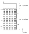
- Fig. 3 is an example of an outline of an IO cell layout.
- the layout of FIG. 3 corresponds to the IO cell 10a, which is one of the IO cells 10 arranged on the lower side of the semiconductor integrated circuit device 1 of FIG.
- An IO cell generally includes a high power supply voltage region including an ESD protection circuit and an output buffer for outputting signals to the outside of the semiconductor integrated circuit device, and a circuit for inputting/outputting signals to/from the semiconductor integrated circuit device. and a low power supply voltage region.
- the IO cell 10a of FIG. 3 is divided into a low power supply voltage area 31 and a high power supply voltage area 32 in the Y direction.
- the X direction is the direction along the outer edge of the semiconductor integrated circuit device 1
- the Y direction is the direction perpendicular to the X direction.
- the low power supply voltage area 31 is on the core area 2 side
- the high power supply voltage area 32 is on the chip edge side.
- the output circuit 11 of FIG. 2 is configured in the IO cell 10a shown in FIG.
- an output transistor N1, an ESD protection diode 1a, an ESD protection diode 1b, and an output transistor P1 are arranged in order from the chip edge.
- Resistive elements RU are arranged in an array in the XY directions above the output transistors N1, P1 and the ESD protection diodes 1a, 1b.
- a protection resistor Rsn is formed by connecting output transistor N1 and resistance element RU arranged above ESD protection diode 1a to each other.
- a protection resistor Rsp is formed by connecting the resistance element RU arranged above the output transistor P1 and the ESD protection diode 1b to each other.
- the connection form of the resistance elements RU may be series connection, parallel connection, or a combination of series connection and parallel connection.
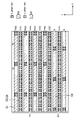
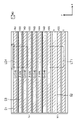
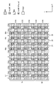
- FIGS. 4 to 8 are plan views showing the details of the layout of the IO cells.
- FIGS. 4 to 8 are hierarchical diagrams showing enlarged portions of the ESD protection diode 1a and the output transistor N1 in FIG.
- FIG. 9 is a cross-sectional view showing the cross-sectional structure taken along line X-X' in FIG.
- FIG. 4 shows the structure of the M5 wiring layer, M4 wiring layer and RMetal wiring layer.
- the RMetal wiring layer is formed between the M4 wiring layer and the M3 wiring layer, and is a wiring layer for forming the resistance element RU.
- the RMetal wiring layer is formed in BEOL (Back End of Line: wiring process).
- the resistance element RU formed in the RMetal wiring layer is connected to the wiring of the M4 wiring layer through vias.
- M5 wirings 21, 22 and 23 extending in the Y direction are formed.
- the M5 wiring 21 corresponds to an external output terminal PAD and is connected to an IO pad (not shown).
- M5 wiring 22 corresponds to node A, and M5 wiring 23 is connected to VSS.
- M4 wirings 26a, 26b and 27 extending in the X direction are formed.
- the M4 wiring 27 is connected to the M5 wiring 23 via vias. That is, the M4 wiring 27 is connected to VSS.
- a resistance element RU is formed in the RMetal wiring layer. Both ends of the resistance element RU in the X direction are connected to the M4 wirings 26a and 26b via vias.
- the M4 wiring 26a is connected to the M5 wiring 21 through a via
- the M4 wiring 26b is connected to the M5 wiring 22 through a via. That is, M5 wiring 21 (PAD) ⁇ via (M5-M4) ⁇ M4 wiring 26a ⁇ via (M4-RMetal) ⁇ resistive element RU ⁇ via (M4-RMetal) ⁇ M4 wiring 26b ⁇ via (M5-M4) ⁇ M5
- a resistance element RU is connected between the external output terminal PAD and the node A through a path of wiring 22(A).
- a protective resistor Rsn is configured by a plurality of resistor elements RU.
- the M4 wiring 27 supplying VSS extends in the X direction between the resistance elements RU in the Y direction. That is, the M4 wiring 27 is not divided by the existence of the resistive element RU.
- FIG. 5 is a lower layer portion of FIG. 4 and shows the structure of the M3 wiring layer and the M2 wiring layer.
- the M3 wiring and the M2 wiring extend in the X direction.
- the vias (M4-M3) and the vias (M3-M2) are formed at the same position in plan view.
- the M2 wiring 51 connected to the external output terminal PAD is connected to the M5 wiring 21 via vias, M3 wiring and M4 wiring.
- the M2 wiring 52 connected to the node A is connected to the M5 wiring 22 through vias, M3 wiring and M4 wiring.
- the M2 wiring 53 and the M3 wiring 54 that supply VSS are arranged at the same position in plan view, and are connected to the M4 wiring 27 via vias.
- the M2 wiring 51 connected to the PAD is connected to the ESD protection diode 1a via the M1 wiring (not shown).
- the M1 wiring is formed at the same position as the M2 wiring 51 in plan view.
- An M2 wiring 54 for supplying VSS is connected to the ESD protection diode 1a via an M1 wiring (not shown).
- the M1 wiring is formed at the same position as the M2 wiring 54 in plan view.
- An M2 wiring 52 connected to the node A is connected to the output transistor N1 via a metal wiring layer and a via (not shown).
- An M2 wiring 54 for supplying VSS is connected to the output transistor N1 via a metal wiring layer and vias (not shown).
- FIG. 6 is a lower layer portion of FIG. 5 and shows the positional relationship between the M2 wiring layer and the anode and cathode of the ESD protection diode 1a.
- the ESD protection diode 1a has a cathode connected to the external output terminal PAD, which overlaps the M2 wiring 51 connected to the external output terminal PAD.
- An anode connected to VSS is arranged at a position overlapping with 53 . That is, the resistance element RU and the cathode of the ESD protection diode 1a are arranged at positions that overlap each other in plan view.
- the arrangement pitch of the cathodes of the ESD protection diodes 1a, the arrangement pitch of the anodes of the ESD protection diodes 1a, and the arrangement pitch of the resistor elements RU are equal in the Y direction.
- FIG. 7 is the layout of the area LD1 in FIG. 6, that is, the ESD protection diode 1a.
- the ESD protection diode 1a includes an anode section 31 formed by a P-conductivity type fin 32 and cathode sections 33a and 33b formed by N-conductivity type fins 34a and 34b.
- the fins 32, 34a, 34b extend in the X direction.
- the anode section 31 is connected to VSS, and the cathode sections 33a and 33b are connected to the external output terminal PAD.
- a diode is formed between the P-type fin 32 and the N-type fins 34a, 34b.
- FIG. 8 is the layout of the area LT1 in FIG. 6, that is, the output transistor N1.
- the output transistors N1 each extend in the X direction and are arranged side by side in the Y direction with a plurality of N conductivity type fins 61 each extending in the Y direction and arranged side by side in the X direction.
- a plurality of gate wirings 62 are formed.
- a fin 61 and a gate wiring 62 that overlap each other in plan view form a transistor.
- Each transistor is connected in parallel by wiring (not shown).
- a drain of each transistor is connected to an external output terminal PAD via a protection resistor Rsn.
- the portions of the ESD protection diode 1b and the output transistor P1 also have the same layout as described above. That is, the layouts of FIGS. 4 to 6 may be reversed vertically (in the Y direction) so that VSS is set to VDD and node A is set to node B.
- FIG. In the case of the ESD protection diode 1b, the cathode connected to VDD is arranged at a position overlapping the M2 wiring that supplies VDD, and the anode is arranged at a position overlapping the M2 wiring connected to the external output terminal PAD. That is, the anode of the ESD protection diode 1b and the resistance element RU are arranged at positions overlapping each other in plan view.
- the arrangement pitch of the cathodes and the arrangement pitch of the anodes in the Y direction be equal to the arrangement pitch of the resistance elements RU.
- FIG. 10 shows the layout of the ESD protection diode 1b.
- the ESD protection diode 1b comprises a cathode portion 36 formed by a fin 37 of N-conductivity type and anode portions 38a and 38b formed by fins 39a and 39b of P-conductivity type.
- the fins 37, 39a, 39b extend in the X direction.
- the cathode section 36 is connected to VDD, and the anode sections 38a and 38b are connected to the external output terminal PAD.
- a diode is formed between the N-type fin 37 and the P-type fins 39a, 39b.
- FIG. 11 shows the layout of the output transistor P1.
- a plurality of P-conductivity type fins 66 each extending in the X direction and arranged side by side in the Y direction, and a plurality of gate wirings 67 each extending in the Y direction and arranged side by side in the X direction are formed. ing.
- Each transistor is connected in parallel by wiring (not shown).
- a drain of each transistor is connected to an external output terminal PAD via a protective resistor Rsp.
- the following effects can be obtained. That is, in the configuration according to this embodiment, of the anodes and cathodes of the ESD protection diodes 1a and 1b, the terminals on the side connected to the power supplies VSS and VDD (that is, the anode of the ESD protection diode 1a and the cathode of the ESD protection diode 1b) ) are arranged so as not to overlap with the resistance element RU. As a result, the resistance of the paths from the power supplies VSS and VDD to the ESD protection diodes 1a and 1b can be suppressed, so that the ESD protection diodes 1a and 1b can be effectively operated and the ESD resistance can be improved. .
- the arrangement pitch of the anodes and cathodes of the ESD protection diodes 1a and 1b and the arrangement pitch of the resistance elements RU are made equal. Therefore, the terminals of the ESD protection diodes 1a and 1b on the side connected to the power supply can be arranged so as to overlap with the upper layer wiring for supplying the power supply in plan view. As a result, since the terminals of the ESD protection diodes 1a and 1b connected to the power supply can be connected directly downward from the upper layer wiring, no connection wiring extending in the Y direction is required. Therefore, the resistance of the paths from the power supply to the ESD protection diodes 1a and 1b can be suppressed.
- the terminals on the side connected to the external signal terminal PAD (that is, the cathode of the ESD protection diode 1a and the anode of the ESD protection diode 1b) are connected to the external signal terminal PAD. It is arranged so as to overlap with the connected wiring (for example, the M4 wiring 26a). As a result, the resistance of the path from the external signal terminal PAD to the ESD protection diodes 1a and 1b can be suppressed, so that the ESD protection diodes 1a and 1b can be effectively operated and the ESD resistance can be improved. .
- FIG. 12 is a circuit configuration diagram of the output circuit 12 according to this embodiment.
- the circuit configuration of FIG. 12 is almost the same as the circuit configuration of FIG. 2 in the first embodiment, but the insertion position of the protective resistor is different. That is, in the output circuit 12 of FIG. 12, a protection resistor Rs is provided instead of the protection resistors Rsn and Rsp in FIG. In FIG. 12, the drains of the output transistors P1 and N1 are connected together, and the protection resistor Rs is provided between the external output terminal PAD and the drains of the output transistors P1 and N1.
- a node C is a node between the drains of the output transistors P1 and N1 and the protection resistor Rs.
- FIG. 13 is an example of an outline of an IO cell layout.
- the IO cell layout of FIG. 13 is similar to the IO cell layout of FIG. 3 in the first embodiment.
- protection resistor Rs is formed by connecting resistor elements RU arranged above output transistors N1, P1 and ESD protection diodes 1a, 1b.
- the connection configuration of the resistance elements RU may be series connection, parallel connection, or a combination of series connection and parallel connection.
- FIG. 14 is a plan view showing details of the layout of the IO cell, and is an enlarged view of the ESD protection diode 1a and the output transistor N1 of FIG.
- FIG. 14 shows the structure of the M5 wiring layer, the M4 wiring layer and the RMetal wiring layer. Note that the configuration and cross-sectional structure of layers below FIG. 14 are the same as those of the first embodiment, and are omitted from illustration here.
- FIG. 14 is the same as the layout of FIG. 4 in the first embodiment. However, the difference is that the M5 wiring 22 corresponds to the node C instead of the node A. 14 is the same as the layout shown in the first embodiment, except that the wiring connected to the node A is connected to the node C.
- FIG. 14 is the same as the layout shown in the first embodiment, except that the wiring connected to the node A is connected to the node C.
- the layout of the portion of the ESD protection diode 1b and the output transistor P1 in FIG. different.
- the M5 wiring 22 in FIG. 14 and the M5 wiring corresponding to the node C in the portion of the ESD protection diode 1b and the output transistor P1 are connected in common.
- terminals of the anodes and cathodes of the ESD protection diodes 1a and 1b, which are connected to the power supplies VSS and VDD, are arranged so as not to overlap the resistance element RU.
- the resistance of the paths from the power supplies VSS and VDD to the ESD protection diodes 1a and 1b can be suppressed, so that the ESD protection diodes 1a and 1b can be effectively operated and the ESD resistance can be improved.
- the arrangement pitch of the anodes and cathodes of the ESD protection diodes 1a and 1b and the arrangement pitch of the resistance elements RU are made equal. Therefore, the terminals of the ESD protection diodes 1a and 1b on the side connected to the power supply can be arranged so as to overlap with the upper layer wiring for supplying the power supply in plan view. As a result, since the terminals of the ESD protection diodes 1a and 1b connected to the power supply can be connected directly downward from the upper layer wiring, no connection wiring extending in the Y direction is required. Therefore, the resistance of the paths from the power supply to the ESD protection diodes 1a and 1b can be suppressed.
- the terminals on the side connected to the external signal terminal PAD (that is, the cathode of the ESD protection diode 1a and the anode of the ESD protection diode 1b) are connected to the external signal terminal PAD. It is arranged so as to overlap with the connected wiring (for example, the M4 wiring 26a). As a result, the resistance of the path from the external signal terminal PAD to the ESD protection diodes 1a and 1b can be suppressed, so that the ESD protection diodes 1a and 1b can be effectively operated and the ESD resistance can be improved. .
- FIG. 15 is an outline of the IO cell layout according to the modification. As shown in FIG. 15, the resistive element RU may be arranged in the low power supply voltage region 31 . This makes it possible to form a protective resistor that requires a larger area.
- the ESD protection diodes 1a, 1b and the output transistors N1, P1 are composed of fins, but they are not limited to this.
- both the P-conductivity type transistor and the N-conductivity type output transistor are one-stage transistors.
- a configuration in which a plurality of stages of transistors such as are connected in series may be used.
- the output circuit in the above-described embodiments may be an input/output circuit including an input circuit.
- the RMetal wiring layer is formed between the M4 wiring layer and the M3 wiring layer, but it is not limited to this.
- the RMetal wiring layer may be formed by BEOL.
- the present disclosure can improve the ESD resistance of a semiconductor integrated circuit device using a resistive element formed in BEOL, and is therefore useful for improving the performance of, for example, a system LSI.
Landscapes
- Semiconductor Integrated Circuits (AREA)
- Metal-Oxide And Bipolar Metal-Oxide Semiconductor Integrated Circuits (AREA)
Priority Applications (2)
| Application Number | Priority Date | Filing Date | Title |
|---|---|---|---|
| JP2023512899A JPWO2022215485A1 (https=) | 2021-04-08 | 2022-03-17 | |
| US18/477,145 US12376384B2 (en) | 2021-04-08 | 2023-09-28 | Semiconductor integrated circuit device |
Applications Claiming Priority (2)
| Application Number | Priority Date | Filing Date | Title |
|---|---|---|---|
| JP2021065885 | 2021-04-08 | ||
| JP2021-065885 | 2021-04-08 |
Related Child Applications (1)
| Application Number | Title | Priority Date | Filing Date |
|---|---|---|---|
| US18/477,145 Continuation US12376384B2 (en) | 2021-04-08 | 2023-09-28 | Semiconductor integrated circuit device |
Publications (1)
| Publication Number | Publication Date |
|---|---|
| WO2022215485A1 true WO2022215485A1 (ja) | 2022-10-13 |
Family
ID=83546379
Family Applications (1)
| Application Number | Title | Priority Date | Filing Date |
|---|---|---|---|
| PCT/JP2022/012403 Ceased WO2022215485A1 (ja) | 2021-04-08 | 2022-03-17 | 半導体集積回路装置 |
Country Status (3)
| Country | Link |
|---|---|
| US (1) | US12376384B2 (https=) |
| JP (1) | JPWO2022215485A1 (https=) |
| WO (1) | WO2022215485A1 (https=) |
Cited By (2)
| Publication number | Priority date | Publication date | Assignee | Title |
|---|---|---|---|---|
| WO2024241869A1 (ja) * | 2023-05-24 | 2024-11-28 | 株式会社ソシオネクスト | 半導体集積回路装置 |
| FR3152638A1 (fr) * | 2023-09-06 | 2025-03-07 | Stmicroelectronics International N.V. | Dispositif de protection ESD pour circuit intégré |
Citations (8)
| Publication number | Priority date | Publication date | Assignee | Title |
|---|---|---|---|---|
| JPH10163433A (ja) * | 1996-11-29 | 1998-06-19 | Nec Corp | 半導体装置における静電保護回路 |
| JP2007150150A (ja) * | 2005-11-30 | 2007-06-14 | Renesas Technology Corp | 半導体装置 |
| JP2010147282A (ja) * | 2008-12-19 | 2010-07-01 | Renesas Technology Corp | 半導体集積回路装置 |
| JP2016072349A (ja) * | 2014-09-29 | 2016-05-09 | ルネサスエレクトロニクス株式会社 | 半導体装置 |
| WO2019043888A1 (ja) * | 2017-08-31 | 2019-03-07 | 株式会社ソシオネクスト | 半導体集積回路装置 |
| WO2019163102A1 (ja) * | 2018-02-23 | 2019-08-29 | 株式会社ソシオネクスト | 半導体装置 |
| US20190304905A1 (en) * | 2018-03-28 | 2019-10-03 | Qualcomm Incorporated | Co-placement of resistor and other devices to improve area & performance |
| JP2020178061A (ja) * | 2019-04-19 | 2020-10-29 | セイコーエプソン株式会社 | 静電気保護回路、半導体装置および電子機器 |
Family Cites Families (1)
| Publication number | Priority date | Publication date | Assignee | Title |
|---|---|---|---|---|
| JP5190913B2 (ja) * | 2007-01-15 | 2013-04-24 | ルネサスエレクトロニクス株式会社 | 半導体集積回路装置 |
-
2022
- 2022-03-17 JP JP2023512899A patent/JPWO2022215485A1/ja active Pending
- 2022-03-17 WO PCT/JP2022/012403 patent/WO2022215485A1/ja not_active Ceased
-
2023
- 2023-09-28 US US18/477,145 patent/US12376384B2/en active Active
Patent Citations (8)
| Publication number | Priority date | Publication date | Assignee | Title |
|---|---|---|---|---|
| JPH10163433A (ja) * | 1996-11-29 | 1998-06-19 | Nec Corp | 半導体装置における静電保護回路 |
| JP2007150150A (ja) * | 2005-11-30 | 2007-06-14 | Renesas Technology Corp | 半導体装置 |
| JP2010147282A (ja) * | 2008-12-19 | 2010-07-01 | Renesas Technology Corp | 半導体集積回路装置 |
| JP2016072349A (ja) * | 2014-09-29 | 2016-05-09 | ルネサスエレクトロニクス株式会社 | 半導体装置 |
| WO2019043888A1 (ja) * | 2017-08-31 | 2019-03-07 | 株式会社ソシオネクスト | 半導体集積回路装置 |
| WO2019163102A1 (ja) * | 2018-02-23 | 2019-08-29 | 株式会社ソシオネクスト | 半導体装置 |
| US20190304905A1 (en) * | 2018-03-28 | 2019-10-03 | Qualcomm Incorporated | Co-placement of resistor and other devices to improve area & performance |
| JP2020178061A (ja) * | 2019-04-19 | 2020-10-29 | セイコーエプソン株式会社 | 静電気保護回路、半導体装置および電子機器 |
Cited By (2)
| Publication number | Priority date | Publication date | Assignee | Title |
|---|---|---|---|---|
| WO2024241869A1 (ja) * | 2023-05-24 | 2024-11-28 | 株式会社ソシオネクスト | 半導体集積回路装置 |
| FR3152638A1 (fr) * | 2023-09-06 | 2025-03-07 | Stmicroelectronics International N.V. | Dispositif de protection ESD pour circuit intégré |
Also Published As
| Publication number | Publication date |
|---|---|
| JPWO2022215485A1 (https=) | 2022-10-13 |
| US12376384B2 (en) | 2025-07-29 |
| US20240038757A1 (en) | 2024-02-01 |
Similar Documents
| Publication | Publication Date | Title |
|---|---|---|
| US10692856B2 (en) | Semiconductor integrated circuit device | |
| US7443224B2 (en) | Multi-threshold MIS integrated circuit device and circuit design method thereof | |
| CN102054834A (zh) | 半导体集成电路器件 | |
| CN110634860A (zh) | 半导体装置 | |
| CN114600242B (zh) | 半导体集成电路装置 | |
| JP3074003B2 (ja) | 半導体集積回路装置 | |
| US12376384B2 (en) | Semiconductor integrated circuit device | |
| US20240213770A1 (en) | Semiconductor integrated circuit device | |
| JP2000223575A (ja) | 半導体装置の設計方法、半導体装置および半導体装置の製造方法 | |
| US7595561B2 (en) | Semiconductor device including multiple rows of peripheral circuit units | |
| US12484312B2 (en) | Semiconductor integrated circuit device | |
| JP3932896B2 (ja) | 半導体装置 | |
| US20250151412A1 (en) | Semiconductor integrated circuit device | |
| US20250192045A1 (en) | Semiconductor integrated circuit device | |
| US20260033012A1 (en) | Semiconductor integrated circuit device | |
| JP7758586B2 (ja) | 半導体集積回路 | |
| WO2025192500A1 (ja) | デカップリング容量素子 | |
| CN119943810A (zh) | 半导体设备 |
Legal Events
| Date | Code | Title | Description |
|---|---|---|---|
| 121 | Ep: the epo has been informed by wipo that ep was designated in this application |
Ref document number: 22784470 Country of ref document: EP Kind code of ref document: A1 |
|
| WWE | Wipo information: entry into national phase |
Ref document number: 2023512899 Country of ref document: JP |
|
| NENP | Non-entry into the national phase |
Ref country code: DE |
|
| 122 | Ep: pct application non-entry in european phase |
Ref document number: 22784470 Country of ref document: EP Kind code of ref document: A1 |