WO2022210401A1 - 積層構造体 - Google Patents
積層構造体 Download PDFInfo
- Publication number
- WO2022210401A1 WO2022210401A1 PCT/JP2022/014563 JP2022014563W WO2022210401A1 WO 2022210401 A1 WO2022210401 A1 WO 2022210401A1 JP 2022014563 W JP2022014563 W JP 2022014563W WO 2022210401 A1 WO2022210401 A1 WO 2022210401A1
- Authority
- WO
- WIPO (PCT)
- Prior art keywords
- layer
- substrate
- laminated structure
- gallium nitride
- nitride film
- Prior art date
- Legal status (The legal status is an assumption and is not a legal conclusion. Google has not performed a legal analysis and makes no representation as to the accuracy of the status listed.)
- Ceased
Links
Images





Classifications
-
- H—ELECTRICITY
- H10—SEMICONDUCTOR DEVICES; ELECTRIC SOLID-STATE DEVICES NOT OTHERWISE PROVIDED FOR
- H10H—INORGANIC LIGHT-EMITTING SEMICONDUCTOR DEVICES HAVING POTENTIAL BARRIERS
- H10H20/00—Individual inorganic light-emitting semiconductor devices having potential barriers, e.g. light-emitting diodes [LED]
- H10H20/80—Constructional details
- H10H20/81—Bodies
- H10H20/822—Materials of the light-emitting regions
- H10H20/824—Materials of the light-emitting regions comprising only Group III-V materials, e.g. GaP
- H10H20/825—Materials of the light-emitting regions comprising only Group III-V materials, e.g. GaP containing nitrogen, e.g. GaN
- H10H20/8252—Materials of the light-emitting regions comprising only Group III-V materials, e.g. GaP containing nitrogen, e.g. GaN characterised by the dopants
-
- C—CHEMISTRY; METALLURGY
- C23—COATING METALLIC MATERIAL; COATING MATERIAL WITH METALLIC MATERIAL; CHEMICAL SURFACE TREATMENT; DIFFUSION TREATMENT OF METALLIC MATERIAL; COATING BY VACUUM EVAPORATION, BY SPUTTERING, BY ION IMPLANTATION OR BY CHEMICAL VAPOUR DEPOSITION, IN GENERAL; INHIBITING CORROSION OF METALLIC MATERIAL OR INCRUSTATION IN GENERAL
- C23C—COATING METALLIC MATERIAL; COATING MATERIAL WITH METALLIC MATERIAL; SURFACE TREATMENT OF METALLIC MATERIAL BY DIFFUSION INTO THE SURFACE, BY CHEMICAL CONVERSION OR SUBSTITUTION; COATING BY VACUUM EVAPORATION, BY SPUTTERING, BY ION IMPLANTATION OR BY CHEMICAL VAPOUR DEPOSITION, IN GENERAL
- C23C14/00—Coating by vacuum evaporation, by sputtering or by ion implantation of the coating forming material
- C23C14/0021—Reactive sputtering or evaporation
- C23C14/0036—Reactive sputtering
-
- C—CHEMISTRY; METALLURGY
- C23—COATING METALLIC MATERIAL; COATING MATERIAL WITH METALLIC MATERIAL; CHEMICAL SURFACE TREATMENT; DIFFUSION TREATMENT OF METALLIC MATERIAL; COATING BY VACUUM EVAPORATION, BY SPUTTERING, BY ION IMPLANTATION OR BY CHEMICAL VAPOUR DEPOSITION, IN GENERAL; INHIBITING CORROSION OF METALLIC MATERIAL OR INCRUSTATION IN GENERAL
- C23C—COATING METALLIC MATERIAL; COATING MATERIAL WITH METALLIC MATERIAL; SURFACE TREATMENT OF METALLIC MATERIAL BY DIFFUSION INTO THE SURFACE, BY CHEMICAL CONVERSION OR SUBSTITUTION; COATING BY VACUUM EVAPORATION, BY SPUTTERING, BY ION IMPLANTATION OR BY CHEMICAL VAPOUR DEPOSITION, IN GENERAL
- C23C14/00—Coating by vacuum evaporation, by sputtering or by ion implantation of the coating forming material
- C23C14/02—Pretreatment of the material to be coated
- C23C14/024—Deposition of sublayers, e.g. to promote adhesion of the coating
-
- C—CHEMISTRY; METALLURGY
- C23—COATING METALLIC MATERIAL; COATING MATERIAL WITH METALLIC MATERIAL; CHEMICAL SURFACE TREATMENT; DIFFUSION TREATMENT OF METALLIC MATERIAL; COATING BY VACUUM EVAPORATION, BY SPUTTERING, BY ION IMPLANTATION OR BY CHEMICAL VAPOUR DEPOSITION, IN GENERAL; INHIBITING CORROSION OF METALLIC MATERIAL OR INCRUSTATION IN GENERAL
- C23C—COATING METALLIC MATERIAL; COATING MATERIAL WITH METALLIC MATERIAL; SURFACE TREATMENT OF METALLIC MATERIAL BY DIFFUSION INTO THE SURFACE, BY CHEMICAL CONVERSION OR SUBSTITUTION; COATING BY VACUUM EVAPORATION, BY SPUTTERING, BY ION IMPLANTATION OR BY CHEMICAL VAPOUR DEPOSITION, IN GENERAL
- C23C14/00—Coating by vacuum evaporation, by sputtering or by ion implantation of the coating forming material
- C23C14/04—Coating on selected surface areas, e.g. using masks
- C23C14/046—Coating cavities or hollow spaces, e.g. interior of tubes; Infiltration of porous substrates
-
- C—CHEMISTRY; METALLURGY
- C23—COATING METALLIC MATERIAL; COATING MATERIAL WITH METALLIC MATERIAL; CHEMICAL SURFACE TREATMENT; DIFFUSION TREATMENT OF METALLIC MATERIAL; COATING BY VACUUM EVAPORATION, BY SPUTTERING, BY ION IMPLANTATION OR BY CHEMICAL VAPOUR DEPOSITION, IN GENERAL; INHIBITING CORROSION OF METALLIC MATERIAL OR INCRUSTATION IN GENERAL
- C23C—COATING METALLIC MATERIAL; COATING MATERIAL WITH METALLIC MATERIAL; SURFACE TREATMENT OF METALLIC MATERIAL BY DIFFUSION INTO THE SURFACE, BY CHEMICAL CONVERSION OR SUBSTITUTION; COATING BY VACUUM EVAPORATION, BY SPUTTERING, BY ION IMPLANTATION OR BY CHEMICAL VAPOUR DEPOSITION, IN GENERAL
- C23C14/00—Coating by vacuum evaporation, by sputtering or by ion implantation of the coating forming material
- C23C14/06—Coating by vacuum evaporation, by sputtering or by ion implantation of the coating forming material characterised by the coating material
- C23C14/0617—AIII BV compounds, where A is Al, Ga, In or Tl and B is N, P, As, Sb or Bi
-
- C—CHEMISTRY; METALLURGY
- C23—COATING METALLIC MATERIAL; COATING MATERIAL WITH METALLIC MATERIAL; CHEMICAL SURFACE TREATMENT; DIFFUSION TREATMENT OF METALLIC MATERIAL; COATING BY VACUUM EVAPORATION, BY SPUTTERING, BY ION IMPLANTATION OR BY CHEMICAL VAPOUR DEPOSITION, IN GENERAL; INHIBITING CORROSION OF METALLIC MATERIAL OR INCRUSTATION IN GENERAL
- C23C—COATING METALLIC MATERIAL; COATING MATERIAL WITH METALLIC MATERIAL; SURFACE TREATMENT OF METALLIC MATERIAL BY DIFFUSION INTO THE SURFACE, BY CHEMICAL CONVERSION OR SUBSTITUTION; COATING BY VACUUM EVAPORATION, BY SPUTTERING, BY ION IMPLANTATION OR BY CHEMICAL VAPOUR DEPOSITION, IN GENERAL
- C23C14/00—Coating by vacuum evaporation, by sputtering or by ion implantation of the coating forming material
- C23C14/06—Coating by vacuum evaporation, by sputtering or by ion implantation of the coating forming material characterised by the coating material
- C23C14/0641—Nitrides
-
- C—CHEMISTRY; METALLURGY
- C23—COATING METALLIC MATERIAL; COATING MATERIAL WITH METALLIC MATERIAL; CHEMICAL SURFACE TREATMENT; DIFFUSION TREATMENT OF METALLIC MATERIAL; COATING BY VACUUM EVAPORATION, BY SPUTTERING, BY ION IMPLANTATION OR BY CHEMICAL VAPOUR DEPOSITION, IN GENERAL; INHIBITING CORROSION OF METALLIC MATERIAL OR INCRUSTATION IN GENERAL
- C23C—COATING METALLIC MATERIAL; COATING MATERIAL WITH METALLIC MATERIAL; SURFACE TREATMENT OF METALLIC MATERIAL BY DIFFUSION INTO THE SURFACE, BY CHEMICAL CONVERSION OR SUBSTITUTION; COATING BY VACUUM EVAPORATION, BY SPUTTERING, BY ION IMPLANTATION OR BY CHEMICAL VAPOUR DEPOSITION, IN GENERAL
- C23C14/00—Coating by vacuum evaporation, by sputtering or by ion implantation of the coating forming material
- C23C14/22—Coating by vacuum evaporation, by sputtering or by ion implantation of the coating forming material characterised by the process of coating
- C23C14/34—Sputtering
- C23C14/3435—Applying energy to the substrate during sputtering
- C23C14/345—Applying energy to the substrate during sputtering using substrate bias
-
- C—CHEMISTRY; METALLURGY
- C30—CRYSTAL GROWTH
- C30B—SINGLE-CRYSTAL GROWTH; UNIDIRECTIONAL SOLIDIFICATION OF EUTECTIC MATERIAL OR UNIDIRECTIONAL DEMIXING OF EUTECTOID MATERIAL; REFINING BY ZONE-MELTING OF MATERIAL; PRODUCTION OF A HOMOGENEOUS POLYCRYSTALLINE MATERIAL WITH DEFINED STRUCTURE; SINGLE CRYSTALS OR HOMOGENEOUS POLYCRYSTALLINE MATERIAL WITH DEFINED STRUCTURE; AFTER-TREATMENT OF SINGLE CRYSTALS OR A HOMOGENEOUS POLYCRYSTALLINE MATERIAL WITH DEFINED STRUCTURE; APPARATUS THEREFOR
- C30B23/00—Single-crystal growth by condensing evaporated or sublimed materials
- C30B23/02—Epitaxial-layer growth
- C30B23/025—Epitaxial-layer growth characterised by the substrate
-
- C—CHEMISTRY; METALLURGY
- C30—CRYSTAL GROWTH
- C30B—SINGLE-CRYSTAL GROWTH; UNIDIRECTIONAL SOLIDIFICATION OF EUTECTIC MATERIAL OR UNIDIRECTIONAL DEMIXING OF EUTECTOID MATERIAL; REFINING BY ZONE-MELTING OF MATERIAL; PRODUCTION OF A HOMOGENEOUS POLYCRYSTALLINE MATERIAL WITH DEFINED STRUCTURE; SINGLE CRYSTALS OR HOMOGENEOUS POLYCRYSTALLINE MATERIAL WITH DEFINED STRUCTURE; AFTER-TREATMENT OF SINGLE CRYSTALS OR A HOMOGENEOUS POLYCRYSTALLINE MATERIAL WITH DEFINED STRUCTURE; APPARATUS THEREFOR
- C30B29/00—Single crystals or homogeneous polycrystalline material with defined structure characterised by the material or by their shape
- C30B29/10—Inorganic compounds or compositions
- C30B29/40—AIIIBV compounds wherein A is B, Al, Ga, In or Tl and B is N, P, As, Sb or Bi
- C30B29/403—AIII-nitrides
- C30B29/406—Gallium nitride
-
- H—ELECTRICITY
- H10—SEMICONDUCTOR DEVICES; ELECTRIC SOLID-STATE DEVICES NOT OTHERWISE PROVIDED FOR
- H10D—INORGANIC ELECTRIC SEMICONDUCTOR DEVICES
- H10D30/00—Field-effect transistors [FET]
- H10D30/01—Manufacture or treatment
- H10D30/021—Manufacture or treatment of FETs having insulated gates [IGFET]
-
- H—ELECTRICITY
- H10—SEMICONDUCTOR DEVICES; ELECTRIC SOLID-STATE DEVICES NOT OTHERWISE PROVIDED FOR
- H10D—INORGANIC ELECTRIC SEMICONDUCTOR DEVICES
- H10D30/00—Field-effect transistors [FET]
- H10D30/01—Manufacture or treatment
- H10D30/061—Manufacture or treatment of FETs having Schottky gates
-
- H—ELECTRICITY
- H10—SEMICONDUCTOR DEVICES; ELECTRIC SOLID-STATE DEVICES NOT OTHERWISE PROVIDED FOR
- H10D—INORGANIC ELECTRIC SEMICONDUCTOR DEVICES
- H10D30/00—Field-effect transistors [FET]
- H10D30/40—FETs having zero-dimensional [0D], one-dimensional [1D] or two-dimensional [2D] charge carrier gas channels
- H10D30/47—FETs having zero-dimensional [0D], one-dimensional [1D] or two-dimensional [2D] charge carrier gas channels having two-dimensional [2D] charge carrier gas channels, e.g. nanoribbon FETs or high electron mobility transistors [HEMT]
- H10D30/471—High electron mobility transistors [HEMT] or high hole mobility transistors [HHMT]
-
- H—ELECTRICITY
- H10—SEMICONDUCTOR DEVICES; ELECTRIC SOLID-STATE DEVICES NOT OTHERWISE PROVIDED FOR
- H10D—INORGANIC ELECTRIC SEMICONDUCTOR DEVICES
- H10D30/00—Field-effect transistors [FET]
- H10D30/60—Insulated-gate field-effect transistors [IGFET]
- H10D30/67—Thin-film transistors [TFT]
-
- H—ELECTRICITY
- H10—SEMICONDUCTOR DEVICES; ELECTRIC SOLID-STATE DEVICES NOT OTHERWISE PROVIDED FOR
- H10D—INORGANIC ELECTRIC SEMICONDUCTOR DEVICES
- H10D30/00—Field-effect transistors [FET]
- H10D30/80—FETs having rectifying junction gate electrodes
- H10D30/87—FETs having Schottky gate electrodes, e.g. metal-semiconductor FETs [MESFET]
-
- H—ELECTRICITY
- H10—SEMICONDUCTOR DEVICES; ELECTRIC SOLID-STATE DEVICES NOT OTHERWISE PROVIDED FOR
- H10D—INORGANIC ELECTRIC SEMICONDUCTOR DEVICES
- H10D62/00—Semiconductor bodies, or regions thereof, of devices having potential barriers
- H10D62/10—Shapes, relative sizes or dispositions of the regions of the semiconductor bodies; Shapes of the semiconductor bodies
- H10D62/17—Semiconductor regions connected to electrodes not carrying current to be rectified, amplified or switched, e.g. channel regions
-
- H—ELECTRICITY
- H10—SEMICONDUCTOR DEVICES; ELECTRIC SOLID-STATE DEVICES NOT OTHERWISE PROVIDED FOR
- H10D—INORGANIC ELECTRIC SEMICONDUCTOR DEVICES
- H10D62/00—Semiconductor bodies, or regions thereof, of devices having potential barriers
- H10D62/80—Semiconductor bodies, or regions thereof, of devices having potential barriers characterised by the materials
- H10D62/85—Semiconductor bodies, or regions thereof, of devices having potential barriers characterised by the materials being Group III-V materials, e.g. GaAs
- H10D62/852—Semiconductor bodies, or regions thereof, of devices having potential barriers characterised by the materials being Group III-V materials, e.g. GaAs being Group III-V materials comprising three or more elements, e.g. AlGaN or InAsSbP
-
- H—ELECTRICITY
- H10—SEMICONDUCTOR DEVICES; ELECTRIC SOLID-STATE DEVICES NOT OTHERWISE PROVIDED FOR
- H10H—INORGANIC LIGHT-EMITTING SEMICONDUCTOR DEVICES HAVING POTENTIAL BARRIERS
- H10H20/00—Individual inorganic light-emitting semiconductor devices having potential barriers, e.g. light-emitting diodes [LED]
- H10H20/80—Constructional details
- H10H20/81—Bodies
- H10H20/819—Bodies characterised by their shape, e.g. curved or truncated substrates
- H10H20/82—Roughened surfaces, e.g. at the interface between epitaxial layers
-
- H—ELECTRICITY
- H10—SEMICONDUCTOR DEVICES; ELECTRIC SOLID-STATE DEVICES NOT OTHERWISE PROVIDED FOR
- H10P—GENERIC PROCESSES OR APPARATUS FOR THE MANUFACTURE OR TREATMENT OF DEVICES COVERED BY CLASS H10
- H10P95/00—Generic processes or apparatus for manufacture or treatments not covered by the other groups of this subclass
-
- H—ELECTRICITY
- H10—SEMICONDUCTOR DEVICES; ELECTRIC SOLID-STATE DEVICES NOT OTHERWISE PROVIDED FOR
- H10D—INORGANIC ELECTRIC SEMICONDUCTOR DEVICES
- H10D62/00—Semiconductor bodies, or regions thereof, of devices having potential barriers
- H10D62/80—Semiconductor bodies, or regions thereof, of devices having potential barriers characterised by the materials
- H10D62/83—Semiconductor bodies, or regions thereof, of devices having potential barriers characterised by the materials being Group IV materials, e.g. B-doped Si or undoped Ge
-
- H—ELECTRICITY
- H10—SEMICONDUCTOR DEVICES; ELECTRIC SOLID-STATE DEVICES NOT OTHERWISE PROVIDED FOR
- H10H—INORGANIC LIGHT-EMITTING SEMICONDUCTOR DEVICES HAVING POTENTIAL BARRIERS
- H10H20/00—Individual inorganic light-emitting semiconductor devices having potential barriers, e.g. light-emitting diodes [LED]
- H10H20/80—Constructional details
- H10H20/81—Bodies
- H10H20/819—Bodies characterised by their shape, e.g. curved or truncated substrates
Definitions
- One embodiment of the present invention relates to a laminated structure including a gallium nitride film formed on a substrate.
- Gallium nitride is characterized as a direct bandgap semiconductor with a large bandgap. Taking advantage of this feature of gallium nitride, light-emitting diodes (LEDs) using gallium nitride have already been put to practical use. In addition, gallium nitride also has the characteristics of high electron saturation mobility and high breakdown voltage. In recent years, utilizing the characteristics of gallium nitride, the development of transistors for high-frequency power devices is underway. Gallium nitride films for light-emitting diodes or transistors are generally formed on sapphire substrates at high temperatures of 800° C. to 1000° C. using MOCVD (Metal Organic Chemical Vapor Deposition) or HVPE (Hydride Vapor Phase Epitaxy).
- MOCVD Metal Organic Chemical Vapor Deposition
- HVPE Hydride Vapor Phase Epitaxy
- Micro LED display or mini LED display has high efficiency, high brightness and high reliability.
- Such a micro-LED display device or mini-LED display device is manufactured by transferring an LED chip to a backplane on which a transistor using an oxide semiconductor or low-temperature polysilicon is formed (see, for example, Patent Documents 1). Further, a method of forming a transistor containing gallium nitride and a light-emitting diode over the same substrate has also been studied (see Patent Document 2, for example).
- gallium nitride films are generally formed on sapphire substrates at high temperatures.
- a large-area substrate such as an amorphous glass substrate has low heat resistance, and a gallium nitride film formed at a low temperature has a problem of low crystallinity.
- Another problem is that it is difficult to provide a large-area backplane.
- one object of an embodiment of the present invention is to provide a laminated structure in which a highly crystalline gallium nitride film is formed on a substrate that can be increased in area.
- a laminated structure according to one embodiment of the present invention includes a substrate and a gallium nitride film on the substrate, and the surface arithmetic mean roughness (Ra) of the substrate is less than 0.33 nm.
- a laminated structure according to one embodiment of the present invention includes a substrate, an orientation layer having c-axis orientation or face-centered cubic (111) orientation on the substrate, and a gallium nitride film on the orientation layer,
- the surface arithmetic mean roughness (Ra) of the substrate is less than 0.33 nm.
- a laminated structure includes a substrate, a protective layer on the substrate, an orientation layer having c-axis orientation or face-centered cubic (111) orientation on the protective layer, and and a gallium nitride film, and the surface arithmetic mean roughness (Ra) of the substrate is less than 0.33 nm.
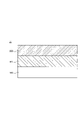
- FIG. 1 is a schematic diagram showing the configuration of a laminated structure according to one embodiment of the present invention
- FIG. 1 is a schematic diagram showing the configuration of a laminated structure according to one embodiment of the present invention
- FIG. 1 is a schematic diagram showing the configuration of a laminated structure according to one embodiment of the present invention
- FIG. 1 is a schematic diagram showing the configuration of a laminated structure according to one embodiment of the present invention
- FIG. 1 is a schematic diagram showing the configuration of a laminated structure according to one embodiment of the present invention
- FIG. 1 is a schematic diagram showing the configuration of a laminated structure according to one embodiment of the present invention
- FIG. 1 is a schematic diagram showing the configuration of a laminated structure according to one embodiment of the present invention
- FIG. 1 is a schematic diagram showing the configuration of a laminated structure according to one embodiment of the present invention
- FIG. 1 is a schematic diagram showing the configuration of a laminated structure according to one embodiment of the present invention
- FIG. 1 is a schematic diagram showing the configuration of a laminated structure according to one embodiment of the present invention
- FIG. 1 is a schematic diagram showing the configuration of a laminated structure according to one embodiment of the present invention
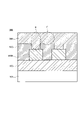
- FIG. 1 is a schematic diagram showing the configuration of a light-emitting device using a laminated structure according to one embodiment of the present invention
- FIG. 1 is a schematic diagram showing the configuration of a semiconductor device using a laminated structure according to one embodiment of the present invention
- ⁇ includes A, B or C
- ⁇ includes any one of A, B and C
- ⁇ includes one selected from the group consisting of A, B and C
- ⁇ does not exclude the case where ⁇ includes a plurality of combinations of A to C, unless otherwise specified.
- these expressions do not exclude the case where ⁇ contains other elements.
- the terms “upper”, “upper”, “lower”, and “lower” are used, but in principle, the substrate on which the structure is formed is used as a reference, and the structure is formed from the substrate. Let the direction toward an object be “up” or “upper”. Conversely, the direction from the structure toward the substrate is defined as “down” or “lower”. Therefore, in the expression of the structure on the substrate, the surface of the structure facing the substrate is the lower surface of the structure, and the opposite surface is the upper surface of the structure.
- the expression “structure on the substrate” merely describes the vertical relationship between the substrate and the structure, and other members may be arranged between the substrate and the structure.
- the terms “upper” or “upper” or “lower” or “lower” mean the order of stacking in a structure in which a plurality of layers are stacked, even if they are not in an overlapping positional relationship in plan view. good.
- FIG. 1 is a schematic diagram showing the configuration of a laminated structure according to one embodiment of the present invention.
- a laminated structure 10 includes a substrate 100 and a gallium nitride film 200 .
- a gallium nitride film 200 is formed on the substrate 100 using sputtering.
- the substrate 100 is a support substrate for the gallium nitride film 200 . Since the gallium nitride film 200 of the laminated structure 10 is formed by sputtering, the substrate 100 may have heat resistance of about 600° C., for example. Therefore, for example, an amorphous glass substrate can be used as the substrate 100 .
- a resin substrate such as a polyimide substrate, an acrylic substrate, a siloxane substrate, or a fluororesin substrate can be used as the substrate 100 .
- a resin substrate such as a polyimide substrate, an acrylic substrate, a siloxane substrate, or a fluororesin substrate can be used. Note that an amorphous glass substrate or a resin substrate is a substrate that can have a large area.
- a polycrystalline substrate can also be used as the substrate 100 . Since the polycrystalline substrate is larger than the sapphire substrate used in normal film formation of gallium nitride films, it can be used as a backplane in the same manner as
- the crystal growth of the gallium nitride film 200 on the substrate 100 such as amorphous glass is affected by the surface state of the substrate 100 .
- unevenness on the surface of the substrate 100 is a factor in generating random crystal nuclei.
- crystal growth of gallium nitride occurs in random directions, and adjacent crystals interfere with each other, inhibiting crystal growth. Therefore, the substrate 100 preferably has a smooth surface with few irregularities.
- the arithmetic mean roughness (Ra) of the surface of substrate 100 is preferably less than 0.33 nm.
- the root mean square roughness (Rq) of the surface of the substrate 100 is preferably less than 0.39 nm.
- the crystallinity of the gallium nitride film 200 can be improved even if the substrate 100 is amorphous and is a glass substrate.
- the gallium nitride film 200 having c-axis orientation (orientation with the (0001) plane as the surface) can be formed on the substrate 100 .
- a substrate 100 is placed in a vacuum chamber facing a gallium nitride target.
- the composition ratio of gallium nitride in the gallium nitride target is preferably 0.7 or more and 2 or less of gallium to nitrogen.
- Nitrogen can also be supplied to the vacuum chamber separately from the sputtering gas (such as argon or krypton). In that case, it is preferable that the composition ratio of gallium nitride in the gallium nitride target is more gallium than nitrogen.
- nitrogen can be supplied using a nitrogen radical source.
- the sputtering power supply can be either a DC power supply, an RF power supply, or a pulsed DC power supply.
- the substrate 100 inside the vacuum chamber may be heated.
- the substrate 100 can be heated at 400.degree. C. or more and less than 600.degree.
- This substrate temperature can be applied to an amorphous glass substrate having low heat resistance. Also, this substrate temperature is lower than the deposition temperature in MOCVD or HVPE.
- the sputtering gas is supplied. Also, a voltage is applied between the substrate 100 and the gallium nitride target at a predetermined pressure to generate plasma, and the gallium nitride film 200 is formed. Since the gallium nitride film 200 is formed on the substrate 100 whose surface roughness is controlled, the gallium nitride film 200 has a c-axis orientation.
- the laminated structure 10 includes a gallium nitride film 200 with high crystallinity and c-axis orientation. Moreover, the laminated structure 10 includes a substrate 100 that can have a large area. Therefore, by using the laminated structure 10, it is possible to increase the productivity of LEDs containing gallium nitride, or to manufacture backplanes on which transistors containing gallium nitride are formed.
- FIG. 2 is a schematic diagram showing the configuration of a laminated structure 20 according to one embodiment of the present invention.
- the laminated structure 20 includes a substrate 100 , an alignment layer 300 and a gallium nitride film 200 .
- An alignment layer 300 is provided on the substrate 100 .
- the gallium nitride film 200 is formed on the alignment layer 300 using sputtering.
- the configuration of the laminated structure 20 is the same as the configuration of the laminated structure 10, the explanation may be omitted.
- the orientation layer 300 can improve the crystallinity of the gallium nitride film 200 . That is, the orientation layer 300 can further improve the c-axis orientation of the gallium nitride film 200 .
- the gallium nitride film 200 having a hexagonal close-packed structure is oriented along the c-axis so as to minimize the surface energy even on the smooth substrate 100 .
- the alignment layer 300 can use a material having a hexagonal close-packed structure, a face-centered cubic structure, or a structure conforming thereto.
- the structure conforming to the hexagonal close-packed structure or the face-centered cubic structure includes a crystal structure in which the c-axis is not 90° with respect to the a-axis and the b-axis.
- a material having a hexagonal close-packed structure or a structure equivalent thereto can be oriented in the (0001) direction, that is, in the c-axis direction with respect to the substrate 100 (hereinafter referred to as the (0001) orientation of the hexagonal close-packed structure or the c-axis orientation. called.).
- materials having a face-centered cubic structure or a structure similar thereto can be oriented in the (111) direction with respect to the substrate 100 (hereinafter referred to as (111) orientation of the face-centered cubic structure).
- the gallium nitride film 200 is also easily c-axis oriented.
- the orientation layer 300 include titanium (Ti), titanium nitride (TiN x ), titanium oxide (TiO x ), graphene, zinc oxide (ZnO), magnesium diboride (MgB 2 ), aluminum (Al), and aluminum nitride.
- AlN aluminum oxide
- Al2O3 aluminum oxide
- silver Ag
- calcium Ca
- nickel Ni
- copper Cu
- strontium Sr
- rhodium Rh
- palladium Pd
- cerium Ce
- ytterbium Yb
- iridium Ir
- platinum Pt
- gold Au
- lead Pb
- actinium Au
- Th lithium niobate
- BiLaTiO SrFeO, SrFeO , BiFeO, BaFeO, ZnFeO, PMnN-PZT, or biogenic apatite (BAp)
- the alignment layer 300 it is preferable to use titanium, graphene, zinc oxide, aluminum nitride, or aluminum oxide as the alignment layer 300 .
- the film thickness of the alignment layer 300 is, for example, 50 nm or more. Note that the deposition of the alignment layer 300 is not limited to sputtering.
- the alignment layer 300 can be deposited using any method (apparatus) such as CVD.
- the crystallinity of the gallium nitride film 200 is affected by the surface state of the non-film-forming surface, as described above. That is, in the laminated structure 20 , the gallium nitride film 200 is affected by the surface state of the orientation layer 300 . Therefore, the alignment layer 300 preferably has a smooth surface with few irregularities.
- the surface arithmetic mean roughness (Ra) of the alignment layer 300 is preferably less than 2.3 nm.
- the root-mean-square roughness (Rq) of the surface of the alignment layer 300 is preferably less than 2.9 nm.
- the substrate 100 preferably has a smooth surface with little unevenness.
- the arithmetic mean roughness (Ra) of the surface of substrate 100 is preferably less than 0.33 nm.
- the root mean square roughness (Rq) of the surface of the substrate 100 is preferably less than 0.39 nm.
- the laminated structure 20 includes a gallium nitride film 200 with high crystallinity and c-axis orientation.
- the laminated structure 20 includes a substrate 100 that can have a large area. Therefore, by using the laminated structure 20, it is possible to increase the productivity of LEDs containing gallium nitride or to fabricate backplanes on which transistors containing gallium nitride are formed.
- FIG. 3 is a schematic diagram showing the configuration of a laminated structure 30 according to one embodiment of the present invention.
- the laminated structure 30 includes a substrate 100 , a protective layer 400 , an alignment layer 300 and a gallium nitride film 200 .
- a protective layer 400 is provided on the substrate 100 .
- the alignment layer 300 is provided on the protective layer 400 .
- the gallium nitride film 200 is formed on the alignment layer 300 using sputtering.
- the structure of the laminated structure 30 is the structure similar to the laminated structure 10 or the laminated structure 20, the description may be abbreviate
- the protective layer 400 can prevent impurities from diffusing from the substrate 100 . Therefore, since the orientation layer 300 formed on the protective layer 400 has few impurities, the crystallinity is improved. Silicon oxide (SiO x ) or silicon nitride (SiN x ), for example, can be used as the protective layer 400 .
- the protective layer 400 may be a single film or a laminated film.
- the substrate 100 is an amorphous glass substrate, a laminated film (SiO x /SiN x ) of silicon nitride and silicon oxide can be used.
- a laminated film (SiO x /SiN x /SiO x ) in which silicon nitride is sandwiched between silicon oxides can be used.
- the orientation layer 300 is formed on the protective layer 400 , so the crystallinity of the orientation layer 300 is affected by the surface roughness of the protective layer 400 . Therefore, in the laminated structure 30, the protective layer 400 preferably has a smooth surface with little unevenness.
- the surface arithmetic mean roughness (Ra) of the protective layer 400 is preferably less than 0.51 nm.
- the root-mean-square roughness (Rq) of the surface of the protective layer 400 is preferably less than 0.60 nm.
- the laminated structure 30 includes a gallium nitride film 200 with high crystallinity and c-axis orientation. Moreover, the laminated structure 30 includes a substrate 100 that can be increased in area. Therefore, by using the laminated structure 20, it is possible to increase the productivity of LEDs containing gallium nitride or to fabricate backplanes on which transistors containing gallium nitride are formed.
- FIG. 4 is a schematic diagram showing the configuration of a laminated structure 30A according to one embodiment of the present invention.
- the laminated structure 30A includes a substrate 100, a protective layer 400, a first alignment layer 300A-1, a second alignment layer 300A-2, and a gallium nitride film 200.
- FIG. A first alignment layer 300 A- 1 is provided on the protective layer 400 .
- a second alignment layer 300A-2 is provided on the first alignment layer 300A-1.
- the gallium nitride film 200 is provided on the second orientation layer 300A-2. That is, the second alignment layer 300A-2 is in contact with the gallium nitride film 200.
- FIG. 1 The laminated structure 30A includes a substrate 100, a protective layer 400, a first alignment layer 300A-1, a second alignment layer 300A-2, and a gallium nitride film 200.
- the first alignment layer 300A-1 and the second alignment layer 300A-2 are different in type of alignment layer.
- the first alignment layer 300A-1 and the second alignment layer 300A-2 are insulators and conductors, respectively.
- the first alignment layer 300A-1 and the second alignment layer 300A-2 may be conductors and insulators, respectively.
- the materials of the alignment layer 300 described above can be used in combination.
- a combination of materials for the first alignment layer 300A-1 and the second alignment layer 300A-2 may be appropriately selected in consideration of the device in which the laminated structure 30A is used.
- the second orientation layer 300A-2 with which the gallium nitride film 200 is in contact is preferably made of a material capable of preventing diffusion of impurities from the first orientation layer 300A-1 to the gallium nitride film 200.
- FIG. The combination of materials of the first orientation layer 300A-1 and the second orientation layer 300A-2 is, for example, but not limited to, aluminum nitride and titanium, titanium nitride and titanium, or titanium oxide and titanium. .
- Each of the first alignment layer 300A-1 and the second alignment layer 300A-2 can also be a conductor, depending on the device in which the laminated structure 30A is used. Moreover, although the laminated structure 30A including two alignment layers has been described in this modified example, the laminated structure 30A may include three or more alignment layers.
- FIG. 5 is a schematic diagram showing the configuration of a laminated structure 30B according to one embodiment of the present invention.
- the laminated structure 30B includes a substrate 100, a protective layer 400, an alignment layer 300B, and a gallium nitride film 200.
- the alignment layer 300B is provided on the protective layer 400.
- the gallium nitride film 200 is provided on the orientation layer 300B.
- the alignment layer 300B is patterned into a predetermined pattern. Patterning of the alignment layer 300B can be performed using, for example, photolithography. As shown in FIG. 5, the alignment layer 300B is patterned such that a portion of the protective layer 400 is exposed. Therefore, the gallium nitride film 200 includes a region A contacting the alignment layer 300B and a region B contacting the protective layer 400B. In the region A, the gallium nitride film 200 is formed on the orientation layer 300B, so crystal growth can be performed while the c-axis orientation is controlled. On the other hand, in the region B, since the gallium nitride film 200 is formed on the protective layer 400, the c-axis orientation is not controlled as compared with the region A.
- the laminated structure 30B includes a region A with high crystallinity and a region B with low crystallinity. Therefore, in the laminated structure 30B, the gallium nitride film 200 including regions with different crystallinity can be formed by patterning the orientation layer 300B.
- FIG. 6 is a schematic diagram showing the configuration of a laminated structure 30C according to one embodiment of the present invention.
- the laminated structure 30C includes a substrate 100, a protective layer 400, a first alignment layer 300C-1, a second alignment layer 300C-2, and a gallium nitride film 200.
- FIG. A first alignment layer 300 C- 1 is provided on the protective layer 400 .
- a second alignment layer 300C-2 is provided on the first alignment layer 300C-1.
- the gallium nitride film 200 is provided on the second orientation layer 300C-2.
- the second alignment layer 300C-2 is patterned into a predetermined pattern. Patterning of the second alignment layer 300C-2 can be performed, for example, using photolithography. As shown in FIG. 6, the second alignment layer 300C-2 is patterned to expose a portion of the first alignment layer 300C-1. Therefore, the gallium nitride film 200 includes a region C contacting the first orientation layer 300C-1 and a region D contacting the second orientation layer 300C-2. Since the surface on which the gallium nitride film 200 is formed differs between the region C and the region D, the degree of crystal growth of the gallium nitride film 200 (for example, the ratio of c-axis orientation (degree of orientation)) differs. Therefore, in the laminated structure 30C, the gallium nitride film 200 including regions with different crystallinity can be formed by patterning the second orientation layer 300C-2.
- FIG. 7 is a schematic diagram showing the configuration of a laminated structure 30D according to one embodiment of the present invention.
- the laminated structure 30D includes a substrate 100, a protective layer 400, a first alignment layer 300D-1, a second alignment layer 300D-2, and a gallium nitride film 200.
- FIG. A first alignment layer 300 D- 1 is provided on the protective layer 400 .
- a second alignment layer 300D-2 is provided on the first alignment layer 300D-1.
- the gallium nitride film 200 is provided on the second orientation layer 300D-2.
- the first alignment layer 300D-1 is patterned into a predetermined pattern.
- the patterning of the first alignment layer 300D-1 can be performed using photolithography, for example.
- the first alignment layer 300D-1 is patterned such that a portion of the protective layer 400 is exposed.
- the exposed part of the protective layer 400 is covered by the second alignment layer 300D-2 together with the first alignment layer 300D-1. That is, the second alignment layer 300D-2 includes a region formed on the first alignment layer 300D-1 and a region formed on the protective layer 400.
- FIG. Each region has a different degree of crystal growth
- the second orientation layer 300D-2 includes regions with different c-axis orientation or surface roughness.
- the gallium nitride film 200 formed on such a second orientation layer 300D-2 also includes regions of different crystallinity corresponding to the respective regions of the second orientation layer 300D-2. Become. Therefore, in the laminated structure 30D, the gallium nitride film 200 including regions with different crystallinity can be formed by patterning the first orientation layer 300D-1.
- the laminated structure 30D When using the laminated structure 30D for a backplane, it is possible to provide a backplane in which the crystallinity of the gallium nitride film 200 is controlled. Further, by using the uneven patterns of the first alignment layer 300D-1 and the second alignment layer 300D-2 as shown in FIG. 7, it is possible to control the light from the light emitting element and improve the light extraction efficiency. can.
- FIG. 8 is a schematic diagram showing the configuration of a laminated structure 40 according to one embodiment of the present invention.
- the laminated structure 30 includes a substrate 100 , a protective layer 400 , an orientation layer 300 , a non-orientation layer 500 and a gallium nitride film 200 .
- the alignment layer 300 is provided on the protective layer 400 .
- a non-orientation layer 500 is provided on the orientation layer 300 .
- the gallium nitride film 200 is formed on the non-oriented layer 500 using sputtering.
- the configuration of the laminated structure 40 is the same as that of the laminated structure 10, the laminated structure 20, and the laminated structure 30, the explanation may be omitted.
- the non-oriented layer 500 can reduce the crystallinity of the gallium nitride film 200 . That is, the gallium nitride film 200 formed on the non-oriented layer 500 has low crystallinity.
- the non-orientation layer 500 for example, an amorphous material such as silicon oxide can be used. By making the non-formation surface of the gallium nitride film 200 amorphous, the crystal growth of the gallium nitride film 200 can be inhibited.
- the non-orientation layer 500 is patterned into a predetermined pattern. Patterning of the non-orientation layer 500 can be performed, for example, using photolithography. As shown in FIG. 8, the non-orientation layer 500 is patterned such that a portion of the orientation layer 300 is exposed. Therefore, the gallium nitride film 200 includes a region E contacting the oriented layer 300 and a region F contacting the non-oriented layer 500 . In region E, crystal growth of gallium nitride film 200 is promoted, and in region F, crystal growth of gallium nitride film 200 is inhibited. That is, the gallium nitride film 200 of the laminated structure 40 includes regions E with high crystallinity and regions F with low crystallinity. Therefore, in the laminated structure 40, by providing the non-oriented layer 500 and patterning the non-oriented layer 500, the gallium nitride film 200 including regions with different crystallinity can be formed.
- FIG. 9 is a schematic diagram showing the configuration of a laminated structure 40E according to one embodiment of the present invention.
- the laminated structure 40E includes a substrate 100, a protective layer 400, an orientation layer 300E, a non-orientation layer 500, and a gallium nitride film 200.
- FIG. The alignment layer 300E is provided on the protective layer 400.
- the non-orientation layer 500 is provided on the orientation layer 300E.
- the gallium nitride film 200 is formed on the non-oriented layer 500 using sputtering.
- the gallium nitride film 200 includes a region E in contact with the oriented layer 300 and a region F in contact with the non-oriented layer 500.
- the gallium nitride film 200 of the laminated structure 40E also includes regions E with high crystallinity and regions F with low crystallinity. Therefore, the gallium nitride film 200 including regions with different crystallinity can be formed also in the laminated structure 40E.
- FIG. 10 is a schematic diagram showing a laminated structure 40F according to one embodiment of the invention.
- a laminated structure 40F includes a substrate 100, a protective layer 400, a non-oriented layer 500F, an oriented layer 300F, and a gallium nitride film 200.
- FIG. A non-orientation layer 500F is provided on the protective layer 400 .
- the orientation layer 300F is provided on the non-orientation layer 500F.
- the gallium nitride film 200 is formed on the orientation layer 300F using sputtering.
- a non-oriented layer 500F having a predetermined pattern is covered with an oriented layer 300F. That is, the alignment layer 300F includes a region formed over the non-alignment layer 500F and a region formed over the protective layer 400. FIG. Each region has a different degree of crystal growth, and the orientation layer 300F includes regions with different c-axis orientations or different surface roughnesses. Further, the gallium nitride film 200 formed on such an orientation layer 300F also includes regions with different crystallinity corresponding to the respective regions of the orientation layer 300F. Therefore, in the laminated structure 40F, the gallium nitride film 200 including regions with different crystallinity can be formed by forming the orientation layer 300F so as to cover the patterned non-orientation layer 500F.
- the laminated structure 40F for a backplane, it is possible to provide a backplane in which the crystallinity of the gallium nitride film 200 is controlled. Moreover, by using the uneven pattern of the non-oriented layer 500F and the oriented layer 300F as shown in FIG. 10, the light from the light emitting element can be controlled and the light extraction efficiency can be improved.
- FIG. 11 is a schematic diagram showing the configuration of a light emitting device 1000 using the laminated structure 30 according to one embodiment of the present invention.
- the light emitting device 1000 includes a laminated structure 30, an n-type semiconductor layer 1040, a light emitting layer 1050, a p-type semiconductor layer 1060, an n-type electrode 1070, and a p-type electrode 1080.
- the light emitting element 1000 is a so-called LED (Light Emitting Diode), but is not limited to this.
- a silicon-doped gallium nitride film or the like can be used as the n-type semiconductor layer 1040 .
- the light-emitting layer 1050 a stacked body in which an indium gallium nitride film and a gallium nitride film are alternately stacked can be used.
- the p-type semiconductor layer 1060 a magnesium-doped gallium nitride film or the like can be used.
- a metal such as indium can be used as the n-type electrode 1070 .
- a metal such as palladium or gold can be used as the p-type electrode 1080 .
- the manufacturing method of the light emitting device 1000 is as follows.
- a silicon-doped gallium nitride film is formed on the laminated structure 30 . Further, an indium gallium nitride film and a gallium nitride film are alternately formed on a silicon-doped gallium nitride film to form a laminate. Further, a magnesium-doped gallium nitride film is formed on the laminate.
- the magnesium-doped gallium film, the laminate, and the silicon-doped gallium nitride film are etched using photolithography to form the p-type semiconductor layer 1060, the light-emitting layer 1050, and the n-type semiconductor layer 1040. .
- etching is performed so as to expose a part of the surface of the silicon-doped gallium nitride film.
- An n-type electrode 1070 and a p-type electrode 1080 are formed on the n-type semiconductor layer 1040 and the p-type semiconductor layer 1060, respectively.
- a silicon-doped gallium nitride film, an indium gallium nitride film, and a magnesium-doped gallium nitride film can be deposited using a sputtering ring.
- a silicon-doped gallium nitride film, an indium gallium nitride film, and a magnesium-doped gallium nitride film can be continuously formed by connecting a plurality of vacuum chambers via a substrate transfer section without breaking the vacuum. can do.
- the light-emitting element 1000 can be manufactured using the laminated structure 30 . Since the laminated structure 30 includes the substrate 100 that can have a large area, and the light-emitting element 1000 is manufactured using a large-area substrate, the manufacturing cost of the light-emitting element 1000 can be suppressed.
- FIG. 12 is a schematic diagram showing the configuration of a semiconductor device 2000 using the laminated structure 30 according to one embodiment of the present invention.
- a semiconductor device 2000 includes a laminated structure 30, a first aluminum gallium nitride layer 2050, a second aluminum gallium nitride layer 2060, a third aluminum gallium nitride layer 2070, a source electrode 2080, a drain electrode and a 2090 , a gate electrode 2100 , a first insulating layer 2110 , a second insulating layer 2120 and a shield electrode 2130 .
- the semiconductor element 2000 is a so-called HEMT (High Electron Mobility Transistor), but is not limited to this.
- An aluminum gallium nitride film can be used as the first aluminum gallium nitride layer 2050 .
- As the second aluminum gallium nitride layer 2060 for example, a silicon-doped aluminum gallium nitride film can be used.
- An aluminum gallium nitride film can be used as the third aluminum gallium nitride layer 2070 .
- a metal such as titanium or aluminum can be used for the source electrode 2080 and the drain electrode 2090, for example.
- a metal such as nickel or gold can be used as the gate electrode 2100, for example.
- As the first insulating layer 2110 for example, a silicon nitride film can be used.
- As the second insulating layer 2120 for example, a silicon oxide film can be used.
- As the shield electrode 2130 for example, laminated metal such as aluminum/titanium (Al/Ti) can be used.
- the manufacturing method of the semiconductor device 2000 is as follows.
- a first aluminum gallium nitride layer 2050 is formed on the laminated structure 30 .
- a silicon-doped aluminum gallium nitride film and an aluminum gallium nitride film are formed on the first aluminum gallium nitride layer 2050 .
- the aluminum gallium nitride film and the silicon-doped aluminum gallium nitride film are then etched using photolithography to form a third aluminum gallium nitride layer 2070 and a second aluminum gallium nitride layer 2060 . At this time, etching is performed so as to partially expose the surface of the silicon-doped aluminum gallium nitride film.
- a source electrode 2080 and a drain electrode 2090 are formed over the second aluminum gallium nitride layer 2060 . Also, a gate electrode 2100 is formed on the third aluminum gallium nitride layer 2070 . A silicon nitride film and a silicon oxide film are sequentially formed to cover the source electrode 2080 , the drain electrode 2090 , and the gate electrode 2100 to form a first insulating layer 2110 and a second insulating layer 2120 . A shield electrode 2130 is formed on the second insulating layer 2120 .
- Aluminum gallium nitride films and silicon-doped aluminum gallium nitride films can be deposited using a sputtering ring.
- the semiconductor element 2000 can be manufactured using the laminated structure 30 . Since the laminated structure 30 includes the substrate 100 that can be increased in area, a large-area backplane in which the semiconductor elements 2000 are integrated can be manufactured.
Landscapes
- Chemical & Material Sciences (AREA)
- Engineering & Computer Science (AREA)
- Materials Engineering (AREA)
- Metallurgy (AREA)
- Organic Chemistry (AREA)
- Chemical Kinetics & Catalysis (AREA)
- Mechanical Engineering (AREA)
- Crystallography & Structural Chemistry (AREA)
- Inorganic Chemistry (AREA)
- Led Devices (AREA)
Priority Applications (2)
| Application Number | Priority Date | Filing Date | Title |
|---|---|---|---|
| JP2023511189A JP7624061B2 (ja) | 2021-03-31 | 2022-03-25 | 積層構造体 |
| US18/469,731 US12610662B2 (en) | 2021-03-31 | 2023-09-19 | Laminated structure |
Applications Claiming Priority (2)
| Application Number | Priority Date | Filing Date | Title |
|---|---|---|---|
| JP2021059368 | 2021-03-31 | ||
| JP2021-059368 | 2021-03-31 |
Related Child Applications (1)
| Application Number | Title | Priority Date | Filing Date |
|---|---|---|---|
| US18/469,731 Continuation US12610662B2 (en) | 2021-03-31 | 2023-09-19 | Laminated structure |
Publications (1)
| Publication Number | Publication Date |
|---|---|
| WO2022210401A1 true WO2022210401A1 (ja) | 2022-10-06 |
Family
ID=83456153
Family Applications (1)
| Application Number | Title | Priority Date | Filing Date |
|---|---|---|---|
| PCT/JP2022/014563 Ceased WO2022210401A1 (ja) | 2021-03-31 | 2022-03-25 | 積層構造体 |
Country Status (3)
| Country | Link |
|---|---|
| US (1) | US12610662B2 (https=) |
| JP (1) | JP7624061B2 (https=) |
| WO (1) | WO2022210401A1 (https=) |
Cited By (2)
| Publication number | Priority date | Publication date | Assignee | Title |
|---|---|---|---|---|
| WO2024181052A1 (ja) * | 2023-03-02 | 2024-09-06 | 株式会社ジャパンディスプレイ | 発光素子、および発光素子を備える表示装置と照明装置 |
| WO2026023247A1 (ja) * | 2024-07-26 | 2026-01-29 | 株式会社ジャパンディスプレイ | 積層構造体および半導体装置 |
Citations (7)
| Publication number | Priority date | Publication date | Assignee | Title |
|---|---|---|---|---|
| JPS5710280A (en) * | 1980-06-23 | 1982-01-19 | Futaba Corp | Gan light emitting element |
| JPH11243229A (ja) * | 1997-12-02 | 1999-09-07 | Murata Mfg Co Ltd | 半導体発光素子、およびその製造方法 |
| JP2000124140A (ja) * | 1998-10-15 | 2000-04-28 | Furukawa Electric Co Ltd:The | 窒化物系iii−v族化合物半導体の結晶成長方法 |
| JP2002255694A (ja) * | 2001-02-26 | 2002-09-11 | Kyocera Corp | 半導体用基板とその製造方法 |
| JP2006316308A (ja) * | 2005-05-11 | 2006-11-24 | Furukawa Co Ltd | Iii族窒化物半導体層の形成方法、iii族窒化物半導体基板の製造方法、iii族窒化物半導体基板 |
| JP2008540315A (ja) * | 2005-05-11 | 2008-11-20 | ノース・キャロライナ・ステイト・ユニヴァーシティ | 極性が制御されたiii族窒化物薄膜及びその製法 |
| WO2009072631A1 (ja) * | 2007-12-05 | 2009-06-11 | Rohm Co., Ltd. | 窒化物半導体素子の製造方法および窒化物半導体素子 |
Family Cites Families (6)
| Publication number | Priority date | Publication date | Assignee | Title |
|---|---|---|---|---|
| DE19855476A1 (de) | 1997-12-02 | 1999-06-17 | Murata Manufacturing Co | Lichtemittierendes Halbleiterelement mit einer Halbleiterschicht auf GaN-Basis, Verfahren zur Herstellung desselben und Verfahren zur Ausbildung einer Halbleiterschicht auf GaN-Basis |
| US9800016B1 (en) * | 2012-04-05 | 2017-10-24 | Soraa Laser Diode, Inc. | Facet on a gallium and nitrogen containing laser diode |
| US8791474B1 (en) | 2013-03-15 | 2014-07-29 | LuxVue Technology Corporation | Light emitting diode display with redundancy scheme |
| US10389331B2 (en) * | 2017-03-24 | 2019-08-20 | Zhuhai Crystal Resonance Technologies Co., Ltd. | Single crystal piezoelectric RF resonators and filters |
| US11049900B2 (en) | 2018-08-30 | 2021-06-29 | Analog Devices, Inc. | Monolithically integrated nanoemitter light source assembly |
| US12457751B2 (en) * | 2021-07-19 | 2025-10-28 | Taiwan Semiconductor Manufacturing Company, Ltd. | Interfacial layer with high texture uniformity for ferroelectric layer enhancement |
-
2022
- 2022-03-25 JP JP2023511189A patent/JP7624061B2/ja active Active
- 2022-03-25 WO PCT/JP2022/014563 patent/WO2022210401A1/ja not_active Ceased
-
2023
- 2023-09-19 US US18/469,731 patent/US12610662B2/en active Active
Patent Citations (7)
| Publication number | Priority date | Publication date | Assignee | Title |
|---|---|---|---|---|
| JPS5710280A (en) * | 1980-06-23 | 1982-01-19 | Futaba Corp | Gan light emitting element |
| JPH11243229A (ja) * | 1997-12-02 | 1999-09-07 | Murata Mfg Co Ltd | 半導体発光素子、およびその製造方法 |
| JP2000124140A (ja) * | 1998-10-15 | 2000-04-28 | Furukawa Electric Co Ltd:The | 窒化物系iii−v族化合物半導体の結晶成長方法 |
| JP2002255694A (ja) * | 2001-02-26 | 2002-09-11 | Kyocera Corp | 半導体用基板とその製造方法 |
| JP2006316308A (ja) * | 2005-05-11 | 2006-11-24 | Furukawa Co Ltd | Iii族窒化物半導体層の形成方法、iii族窒化物半導体基板の製造方法、iii族窒化物半導体基板 |
| JP2008540315A (ja) * | 2005-05-11 | 2008-11-20 | ノース・キャロライナ・ステイト・ユニヴァーシティ | 極性が制御されたiii族窒化物薄膜及びその製法 |
| WO2009072631A1 (ja) * | 2007-12-05 | 2009-06-11 | Rohm Co., Ltd. | 窒化物半導体素子の製造方法および窒化物半導体素子 |
Cited By (2)
| Publication number | Priority date | Publication date | Assignee | Title |
|---|---|---|---|---|
| WO2024181052A1 (ja) * | 2023-03-02 | 2024-09-06 | 株式会社ジャパンディスプレイ | 発光素子、および発光素子を備える表示装置と照明装置 |
| WO2026023247A1 (ja) * | 2024-07-26 | 2026-01-29 | 株式会社ジャパンディスプレイ | 積層構造体および半導体装置 |
Also Published As
| Publication number | Publication date |
|---|---|
| JPWO2022210401A1 (https=) | 2022-10-06 |
| US20240030384A1 (en) | 2024-01-25 |
| JP7624061B2 (ja) | 2025-01-29 |
| US12610662B2 (en) | 2026-04-21 |
Similar Documents
| Publication | Publication Date | Title |
|---|---|---|
| KR102625489B1 (ko) | 마이크로 led 표시 패널 및 그 제조 방법 | |
| US12610662B2 (en) | Laminated structure | |
| TWI729612B (zh) | 主動矩陣led陣列前驅物 | |
| US20250359400A1 (en) | Light-emitting element and display device and lighting device including the light-emitting element | |
| US20240379730A1 (en) | Light emitting device | |
| US20240274648A1 (en) | Display device and manufacturing method thereof | |
| WO2024116849A1 (ja) | 整流素子 | |
| JP7592881B2 (ja) | アモルファス基板上の窒化ガリウム系半導体デバイス | |
| WO2024185340A1 (ja) | 半導体装置およびその製造方法 | |
| JP7703702B2 (ja) | 発光装置および発光装置形成基板 | |
| JP7669508B2 (ja) | 発光装置および発光装置形成基板 | |
| JP7607140B2 (ja) | 発光装置および発光装置形成基板 | |
| JP7833817B2 (ja) | 積層構造体及びその製造方法、ならびに半導体デバイス | |
| JP7831879B2 (ja) | 半導体デバイス及びその製造方法 | |
| WO2026018570A1 (ja) | 積層構造体 | |
| US20250220999A1 (en) | Laminated structure, method for manufacturing laminated structure, and semiconductor device | |
| TWI859601B (zh) | 發光元件、其製造方法及包含其之顯示裝置 | |
| US20250201554A1 (en) | Multilayer structure, method for producing multilayer structure and semiconductor device | |
| WO2025169644A1 (ja) | 発光素子および発光素子の製造方法 | |
| WO2024048004A1 (ja) | 積層構造体、半導体デバイス及びその製造方法 | |
| WO2024029181A1 (ja) | トランジスタ | |
| WO2023228605A1 (ja) | 積層構造体とその作製方法、および積層構造体を含む半導体装置 | |
| WO2026023247A1 (ja) | 積層構造体および半導体装置 | |
| WO2023037795A1 (ja) | トランジスタ |
Legal Events
| Date | Code | Title | Description |
|---|---|---|---|
| 121 | Ep: the epo has been informed by wipo that ep was designated in this application |
Ref document number: 22780614 Country of ref document: EP Kind code of ref document: A1 |
|
| WWE | Wipo information: entry into national phase |
Ref document number: 2023511189 Country of ref document: JP |
|
| NENP | Non-entry into the national phase |
Ref country code: DE |
|
| 122 | Ep: pct application non-entry in european phase |
Ref document number: 22780614 Country of ref document: EP Kind code of ref document: A1 |