WO2022210083A1 - 液晶光制御装置 - Google Patents
液晶光制御装置 Download PDFInfo
- Publication number
- WO2022210083A1 WO2022210083A1 PCT/JP2022/013099 JP2022013099W WO2022210083A1 WO 2022210083 A1 WO2022210083 A1 WO 2022210083A1 JP 2022013099 W JP2022013099 W JP 2022013099W WO 2022210083 A1 WO2022210083 A1 WO 2022210083A1
- Authority
- WO
- WIPO (PCT)
- Prior art keywords
- liquid crystal
- crystal cell
- electrode
- strip
- substrate
- Prior art date
- Legal status (The legal status is an assumption and is not a legal conclusion. Google has not performed a legal analysis and makes no representation as to the accuracy of the status listed.)
- Ceased
Links
Images







Classifications
-
- G—PHYSICS
- G02—OPTICS
- G02F—OPTICAL DEVICES OR ARRANGEMENTS FOR THE CONTROL OF LIGHT BY MODIFICATION OF THE OPTICAL PROPERTIES OF THE MEDIA OF THE ELEMENTS INVOLVED THEREIN; NON-LINEAR OPTICS; FREQUENCY-CHANGING OF LIGHT; OPTICAL LOGIC ELEMENTS; OPTICAL ANALOGUE/DIGITAL CONVERTERS
- G02F1/00—Devices or arrangements for the control of the intensity, colour, phase, polarisation or direction of light arriving from an independent light source, e.g. switching, gating or modulating; Non-linear optics
- G02F1/01—Devices or arrangements for the control of the intensity, colour, phase, polarisation or direction of light arriving from an independent light source, e.g. switching, gating or modulating; Non-linear optics for the control of the intensity, phase, polarisation or colour
- G02F1/13—Devices or arrangements for the control of the intensity, colour, phase, polarisation or direction of light arriving from an independent light source, e.g. switching, gating or modulating; Non-linear optics for the control of the intensity, phase, polarisation or colour based on liquid crystals, e.g. single liquid crystal display cells
- G02F1/133—Constructional arrangements; Operation of liquid crystal cells; Circuit arrangements
- G02F1/1333—Constructional arrangements; Manufacturing methods
- G02F1/1347—Arrangement of liquid crystal layers or cells in which the final condition of one light beam is achieved by the addition of the effects of two or more layers or cells
- G02F1/13471—Arrangement of liquid crystal layers or cells in which the final condition of one light beam is achieved by the addition of the effects of two or more layers or cells in which all the liquid crystal cells or layers remain transparent, e.g. FLC, ECB, DAP, HAN, TN, STN, SBE-LC cells
-
- G—PHYSICS
- G02—OPTICS
- G02F—OPTICAL DEVICES OR ARRANGEMENTS FOR THE CONTROL OF LIGHT BY MODIFICATION OF THE OPTICAL PROPERTIES OF THE MEDIA OF THE ELEMENTS INVOLVED THEREIN; NON-LINEAR OPTICS; FREQUENCY-CHANGING OF LIGHT; OPTICAL LOGIC ELEMENTS; OPTICAL ANALOGUE/DIGITAL CONVERTERS
- G02F1/00—Devices or arrangements for the control of the intensity, colour, phase, polarisation or direction of light arriving from an independent light source, e.g. switching, gating or modulating; Non-linear optics
- G02F1/01—Devices or arrangements for the control of the intensity, colour, phase, polarisation or direction of light arriving from an independent light source, e.g. switching, gating or modulating; Non-linear optics for the control of the intensity, phase, polarisation or colour
- G02F1/13—Devices or arrangements for the control of the intensity, colour, phase, polarisation or direction of light arriving from an independent light source, e.g. switching, gating or modulating; Non-linear optics for the control of the intensity, phase, polarisation or colour based on liquid crystals, e.g. single liquid crystal display cells
- G02F1/133—Constructional arrangements; Operation of liquid crystal cells; Circuit arrangements
- G02F1/1333—Constructional arrangements; Manufacturing methods
- G02F1/1343—Electrodes
- G02F1/134309—Electrodes characterised by their geometrical arrangement
-
- G—PHYSICS
- G02—OPTICS
- G02F—OPTICAL DEVICES OR ARRANGEMENTS FOR THE CONTROL OF LIGHT BY MODIFICATION OF THE OPTICAL PROPERTIES OF THE MEDIA OF THE ELEMENTS INVOLVED THEREIN; NON-LINEAR OPTICS; FREQUENCY-CHANGING OF LIGHT; OPTICAL LOGIC ELEMENTS; OPTICAL ANALOGUE/DIGITAL CONVERTERS
- G02F1/00—Devices or arrangements for the control of the intensity, colour, phase, polarisation or direction of light arriving from an independent light source, e.g. switching, gating or modulating; Non-linear optics
- G02F1/01—Devices or arrangements for the control of the intensity, colour, phase, polarisation or direction of light arriving from an independent light source, e.g. switching, gating or modulating; Non-linear optics for the control of the intensity, phase, polarisation or colour
- G02F1/13—Devices or arrangements for the control of the intensity, colour, phase, polarisation or direction of light arriving from an independent light source, e.g. switching, gating or modulating; Non-linear optics for the control of the intensity, phase, polarisation or colour based on liquid crystals, e.g. single liquid crystal display cells
- G02F1/133—Constructional arrangements; Operation of liquid crystal cells; Circuit arrangements
- G02F1/1333—Constructional arrangements; Manufacturing methods
- G02F1/1347—Arrangement of liquid crystal layers or cells in which the final condition of one light beam is achieved by the addition of the effects of two or more layers or cells
-
- G—PHYSICS
- G02—OPTICS
- G02F—OPTICAL DEVICES OR ARRANGEMENTS FOR THE CONTROL OF LIGHT BY MODIFICATION OF THE OPTICAL PROPERTIES OF THE MEDIA OF THE ELEMENTS INVOLVED THEREIN; NON-LINEAR OPTICS; FREQUENCY-CHANGING OF LIGHT; OPTICAL LOGIC ELEMENTS; OPTICAL ANALOGUE/DIGITAL CONVERTERS
- G02F1/00—Devices or arrangements for the control of the intensity, colour, phase, polarisation or direction of light arriving from an independent light source, e.g. switching, gating or modulating; Non-linear optics
- G02F1/01—Devices or arrangements for the control of the intensity, colour, phase, polarisation or direction of light arriving from an independent light source, e.g. switching, gating or modulating; Non-linear optics for the control of the intensity, phase, polarisation or colour
- G02F1/13—Devices or arrangements for the control of the intensity, colour, phase, polarisation or direction of light arriving from an independent light source, e.g. switching, gating or modulating; Non-linear optics for the control of the intensity, phase, polarisation or colour based on liquid crystals, e.g. single liquid crystal display cells
- G02F1/133—Constructional arrangements; Operation of liquid crystal cells; Circuit arrangements
- G02F1/1333—Constructional arrangements; Manufacturing methods
- G02F1/1343—Electrodes
- G02F1/134309—Electrodes characterised by their geometrical arrangement
- G02F1/134336—Matrix
Definitions
- One embodiment of the present invention relates to a device that uses the electro-optical effect of liquid crystals to control the light distribution of light emitted from a light source.
- a technology is known that uses a liquid crystal cell to control the light distribution of light emitted from a light source.
- a technique of controlling the light distribution of light emitted from a light source by superimposing a plurality of liquid crystal cells has been disclosed (see Patent Documents 1 and 2, for example).
- Light distribution control using a liquid crystal cell controls the angle of light distribution according to the magnitude of the voltage applied to the liquid crystal cell. By stacking a plurality of liquid crystal cells, it is possible to increase the number of light distribution patterns.
- An object of one embodiment of the present invention is to provide a liquid crystal light control device capable of eliminating moire and non-uniformity in brightness (color unevenness).
- a liquid crystal light control device includes a first liquid crystal cell and a second liquid crystal cell overlapping the first liquid crystal cell, each of the first liquid crystal cell and the second liquid crystal cell having a band-like pattern.
- a first substrate provided with a first electrode including a strip pattern
- a second substrate provided with a second electrode including a strip pattern
- a liquid crystal layer between the first substrate and the second substrate, the first electrode and the longitudinal direction of the strip pattern of the second electrode intersect at an angle of 45° ⁇ 10°.
- a liquid crystal light control device includes a first liquid crystal cell, a second liquid crystal cell overlapping with the first liquid crystal cell, a third liquid crystal cell overlapping with the second liquid crystal cell, and an overlapping third liquid crystal cell. and a fourth liquid crystal cell, wherein each of the first liquid crystal cell, the second liquid crystal cell, the third liquid crystal cell, and the fourth liquid crystal cell includes a first substrate provided with a first electrode including a strip-shaped pattern; a second substrate provided with a second electrode including a pattern; and a liquid crystal layer between the first substrate and the second substrate, wherein the longitudinal direction of the strip pattern of the first electrode and the second electrode is 45 degrees ⁇ They are arranged to intersect at an angle in the range of 10 degrees.
- FIG. 1 shows a perspective view of a liquid crystal light control device according to an embodiment of the present invention
- FIG. FIG. 2 shows a developed view of a liquid crystal light control element that constitutes a liquid crystal light control device according to an embodiment of the present invention.
- 1 shows the arrangement of electrodes of a first liquid crystal cell, a second liquid crystal cell, a third liquid crystal cell, and a fourth liquid crystal cell that constitute a liquid crystal light control element according to an embodiment of the present invention
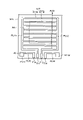
- FIG. 2 is a plan view showing electrodes provided on the first substrate of the liquid crystal cell that constitutes the liquid crystal light control element according to one embodiment of the present invention
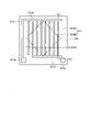
- FIG. 4 is a plan view showing electrodes provided on the second substrate of the liquid crystal cell that constitutes the liquid crystal light control element according to one embodiment of the present invention.
- FIG. 1 shows an example of a cross-sectional structure of a liquid crystal cell that constitutes a liquid crystal light control element according to an embodiment of the present invention.
- FIG. 2 is a plan view showing electrodes provided on the first substrate of the liquid crystal cell that constitutes the liquid crystal light control element according to one embodiment of the present invention;
- FIG. 4 is a plan view showing electrodes provided on the second substrate of the liquid crystal cell that constitutes the liquid crystal light control element according to one embodiment of the present invention.
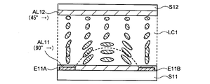
- FIG. 4 is a diagram for explaining the operation of the liquid crystal cell that constitutes the liquid crystal light control element according to one embodiment of the present invention, and shows the alignment state of the liquid crystal molecules when no voltage is applied.
- FIG. 4 is a diagram for explaining the operation of the liquid crystal cell that constitutes the liquid crystal light control element according to one embodiment of the present invention, and shows the alignment state of the liquid crystal molecules when a voltage is applied.
- FIG. 4 is a diagram for explaining the operation of a liquid crystal cell that constitutes the liquid crystal light control element according to one embodiment of the present invention, and shows waveforms of control signals that are applied to electrodes that drive the liquid crystal.
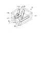
- FIG. 4B is a diagram for explaining the operation of the liquid crystal cell that constitutes the liquid crystal light control element according to the embodiment of the present invention, and shows a perspective view showing the arrangement of the first electrode and the second electrode.
- FIG. 4 is a diagram for explaining the operation of the liquid crystal cell that constitutes the liquid crystal light control element according to one embodiment of the present invention, and shows the alignment state of liquid crystal molecules when a voltage is applied to the first electrode.
- FIG. 4 is a diagram for explaining the operation of the liquid crystal cell that constitutes the liquid crystal light control element according to the embodiment of the present invention, and shows the alignment state of the liquid crystal molecules when a voltage is applied to the second electrode.
- FIG. 2 shows directions in which a first polarized component and a second polarized component are diffused by a liquid crystal cell constituting a liquid crystal light control element according to an embodiment of the present invention;
- FIG. 1 shows directions in which a first polarized component and a second polarized component are diffused by a liquid crystal cell constituting a liquid crystal light control element according to an embodiment of the present invention
- 4 shows the configuration and diffusion state of a liquid crystal light control element according to an embodiment of the present invention
- 4 shows the configuration and diffusion state of a liquid crystal light control element according to an embodiment of the present invention
- 4 shows the configuration and diffusion state of a liquid crystal light control element according to an embodiment of the present invention
- 4 shows the configuration and diffusion state of a liquid crystal light control element according to an embodiment of the present invention
- 4 shows the configuration and diffusion state of a liquid crystal light control element according to an embodiment of the present invention
- a member or region when a member or region is “above (or below)” another member or region, it means directly above (or directly below) the other member or region unless otherwise specified. Includes not only one case but also the case above (or below) another member or region, that is, the case where another component is included between above (or below) another member or region .
- optical rotation refers to a phenomenon in which a linearly polarized light component rotates its polarization axis when passing through the liquid crystal layer.
- the “alignment direction” of the alignment film refers to the direction in which liquid crystal molecules are aligned on the alignment film by performing a treatment (for example, rubbing treatment or photo-alignment treatment) to impart an alignment regulating force to the alignment film. , the direction in which the liquid crystal molecules are aligned.
- a treatment for example, rubbing treatment or photo-alignment treatment
- the alignment direction of the alignment film is usually the rubbing direction.
- the "longitudinal direction" of a strip pattern refers to the direction in which the long side of a pattern having a short side (width) and a long side (length) extends when the strip pattern is viewed from above.
- the band-like pattern includes a pattern that is rectangular in plan view, and also includes a pattern that is bent or curved at least once in the middle of the long side.
- FIG. 1 shows a perspective view of a liquid crystal light control device 100 according to one embodiment of the present invention.
- the liquid crystal light control device 100 includes a liquid crystal light control element 102 and a circuit board 104 .
- Liquid crystal light control element 102 includes a plurality of liquid crystal cells.
- the liquid crystal light control element 102 is preferably composed of a plurality of liquid crystal cells, such as two liquid crystal cells or four liquid crystal cells.
- FIG. 1 shows an example in which the liquid crystal light control element 102 is composed of a first liquid crystal cell 10, a second liquid crystal cell 20, a third liquid crystal cell 30, and a fourth liquid crystal cell 40.
- the first liquid crystal cell 10, the second liquid crystal cell 20, the third liquid crystal cell 30, and the fourth liquid crystal cell 40 are flat panels, and are arranged so that the flat surfaces of the respective liquid crystal cells overlap.
- Transparent adhesive layers are provided between the first liquid crystal cell 10 and the second liquid crystal cell 20, between the second liquid crystal cell 20 and the third liquid crystal cell 30, and between the third liquid crystal cell 30 and the fourth liquid crystal cell 40.
- the liquid crystal light control element 102 has a structure in which liquid crystal cells arranged adjacent to each other in the front and rear are adhered with a transparent adhesive layer.
- the circuit board 104 includes circuits for driving the liquid crystal light control element 102 .
- the first liquid crystal cell 10 is connected to the circuit board 104 through the first flexible wiring board F1
- the second liquid crystal cell 20 is connected to the circuit board 104 through the second flexible wiring board F2
- the third liquid crystal cell 30 is connected to the third flexible wiring.
- the substrate F3 is connected to the circuit board 104
- the fourth liquid crystal cell 40 is connected to the circuit board 104 by the fourth flexible wiring board F4.
- the circuit board 104 outputs a control signal for controlling the alignment state of the liquid crystal to each liquid crystal cell through the flexible wiring board.
- the liquid crystal light control device 100 is configured such that the light emitted from the light source section 106 is emitted to the front side of the drawing through the liquid crystal light control element 102 .
- the first liquid crystal cell 10 the second liquid crystal cell 20, the third liquid crystal cell 30, and the fourth liquid crystal cell 40 are arranged in this order from the light source section 106 side.
- the light source unit 106 includes a white light source, and an optical element such as a lens may be arranged between the white light source and the liquid crystal light control element 102 as necessary.
- the white light source is a light source that emits light close to natural light, and may emit dimmed light such as daylight white or incandescent light.
- the light source unit 106 is desirably composed of a light source having a narrow light distribution range.
- the liquid crystal light control device 100 has a function of controlling the diffusion direction of light emitted from the light source section 106 by means of the liquid crystal light control element 102 .
- the liquid crystal light control element 102 can make the light emitted from the light source section 106 into a predetermined light distribution pattern such as a square shape or a line shape.
- FIG. 2 shows a developed view of the liquid crystal light control element 102 shown in FIG.
- the liquid crystal light control element 102 shows an example including a first liquid crystal cell 10 , a second liquid crystal cell 20 , a third liquid crystal cell 30 and a fourth liquid crystal cell 40 .
- the liquid crystal light control element 102 is not limited to the illustrated configuration, and may be composed of two liquid crystal cells, the first liquid crystal cell 10 and the second liquid crystal cell 20, for example.
- the first liquid crystal cell 10 includes a first substrate S11 and a second substrate S12.
- the first substrate S11 and the second substrate S12 face each other and are arranged with a gap therebetween.
- a liquid crystal layer (not shown) is provided in the gap between the first substrate S11 and the second substrate S12.
- the first flexible wiring board F1 is connected to connection terminals provided on the first board S11, for example.
- the second liquid crystal cell 20 includes a first substrate S21, a second substrate S22, and a second flexible wiring substrate F2, and has the same configuration as the first liquid crystal cell 10.
- the third liquid crystal cell 30 includes a first substrate S31, a second substrate S32, and a third flexible wiring substrate F3, and has the same configuration as the first liquid crystal cell 10.
- FIG. The fourth liquid crystal cell 40 includes a first substrate S41, a second substrate S42, and a fourth flexible wiring substrate F4, and has the same configuration as the first liquid crystal cell 10.
- a first transparent adhesive layer TA1 is provided between the first liquid crystal cell 10 and the second liquid crystal cell 20.
- the first transparent adhesive layer TA1 transmits visible light and is provided to bond the second substrate S12 of the first liquid crystal cell 10 and the first substrate S21 of the second liquid crystal cell 20 together.
- a second transparent adhesive layer TA2 is provided between the second liquid crystal cell 20 and the third liquid crystal cell 30 .
- the second transparent adhesive layer TA2 transmits visible light and is provided to bond the second substrate S22 of the second liquid crystal cell 20 and the first substrate S31 of the third liquid crystal cell 30 together.
- a third transparent adhesive layer TA3 is provided between the third liquid crystal cell 30 and the fourth liquid crystal cell 40 .
- the third transparent adhesive layer TA3 transmits visible light and is provided to bond the second substrate S32 of the third liquid crystal cell 30 and the first substrate S41 of the fourth liquid crystal cell 40 together.
- the first transparent adhesive layer TA1, the second transparent adhesive layer TA2, and the third transparent adhesive layer TA3 have a high transmittance, and have refractive indices of the first substrates S11, S21, S31, S41 and the second substrates S12, S22, S23, A value close to S24 is preferable.
- an optical elastic resin can be used. can be done.
- the thermal expansion coefficients of the first transparent adhesive layer TA1, the second transparent adhesive layer TA2, and the third transparent adhesive layer TA3 are It preferably has a value close to the thermal expansion coefficients of the first substrate and the second substrate.
- the first liquid crystal cell 10, the second liquid crystal cell 20, the third liquid crystal cell 30, and the fourth liquid crystal cell 40 have substantially the same structure except for the configuration of the electrodes.
- the liquid crystal light control element 102 according to this embodiment is arranged so that the electrodes of the first liquid crystal cell 10 on the first substrate S11 side and the electrodes of the substrates of the third liquid crystal cell 30 on the first substrate S31 side intersect.
- the patterns of the corresponding electrodes of the first liquid crystal cell 10 and the third liquid crystal cell 30 may be formed so as to cross each other, or as shown in FIG. 30 may be rotated by a predetermined angle (90 degrees in this embodiment).
- Each liquid crystal cell that constitutes the liquid crystal light control element 102 has strip-shaped electrodes arranged side by side on the main surface of the substrate, and the strip-shaped electrodes generate a lateral electric field.
- the strip-shaped electrodes are not oriented in the same direction in all the liquid crystal cells, but in the range of 0 degrees to 180 degrees for the first substrate and the second substrate of each liquid crystal cell when a certain direction is 0 degrees. placed in a tilted (rotated) state.
- the liquid crystal light control element 102 according to the present embodiment can suppress the occurrence of moire and non-uniformity in brightness (color unevenness) by devising the arrangement of the electrode patterns of the liquid crystal cells. The details are described below.
- FIG. 3 is a development view schematically showing the arrangement of electrodes provided in each of the first liquid crystal cell 10, the second liquid crystal cell 20, the third liquid crystal cell 30, and the fourth liquid crystal cell 40.
- FIG. FIG. 3 shows the electrode arrangement of the first liquid crystal cell 10, the second liquid crystal cell 20, the third liquid crystal cell 30, and the fourth liquid crystal cell 40 in order from the bottom.
- FIG. 3 shows the strip-shaped electrodes provided on the first substrate and the second substrate of each liquid crystal cell viewed from the second substrate side.
- the first liquid crystal cell 10 has a first electrode E11 provided on the first substrate S11 and a second electrode E12 provided on the second substrate S12.
- the first electrode E11 includes a plurality of first strip-shaped electrodes E11A and second strip-shaped electrodes E11B formed in strips. The first strip electrodes E11A and the second strip electrodes E11B are alternately arranged.
- the second electrode E12 includes a plurality of third strip-shaped electrodes E12A and fourth strip-shaped electrodes E12B formed in strips. The third strip-shaped electrodes E12A and the fourth strip-shaped electrodes E12B are alternately arranged.
- the first substrate S11 and the second substrate S12 are arranged to face each other, and it is also possible to define the facing surface as the inner surface and the surface opposite to the inner surface as the outer surface.
- the first electrode E11 is provided on the inner surface of the first substrate S11
- the second electrode E12 is provided on the inner surface of the second substrate S12.
- the second liquid crystal cell 20 the third liquid crystal cell 30, and the fourth liquid crystal cell 40 described below.
- the second liquid crystal cell 20 has a first electrode E21 and a second electrode E22
- the third liquid crystal cell 30 has a first electrode E31 and a second electrode E32
- the fourth liquid crystal cell 40 has a first electrode E41 and a second electrode E32. It has two electrodes E42.
- the first electrodes E21, E31, E41 and the second electrodes E22, E32, E42 each have a plurality of strip-shaped electrodes.
- the longitudinal direction of the first electrode E11 of the first liquid crystal cell 10 (longitudinal direction of the first strip-shaped electrode E11A and the second strip-shaped electrode E11B) is parallel to 90 to 270 degrees (90 degrees to 270 degrees in the figure). The same applies hereinafter), and the longitudinal direction of the second electrode E21 (longitudinal direction of the third strip electrode E12A and the fourth strip electrode E12B) is arranged in a direction parallel to 45 to 225 degrees.
- the longitudinal direction of the first electrode E21 is arranged in a direction parallel to 135-315 degrees
- the second electrode E21 is arranged in a direction parallel to 90-270 degrees
- the third liquid crystal The cell 30 has the first electrode E31 arranged in a direction parallel to 0-180 degrees
- the second electrode E32 arranged in a direction parallel to 135-315
- the fourth liquid crystal cell 40 has the first electrode E41 arranged in a direction parallel to 45 degrees. They are arranged in a direction parallel to -225 degrees
- the second electrodes E42 are arranged in a direction parallel to 0-180 degrees.
- the first electrode E11 of the first liquid crystal cell 10 and the first electrode E31 of the third liquid crystal cell 30 are arranged to E12 is arranged to intersect the second electrode E32 of the third liquid crystal cell 30.
- the first electrode E21 of the second liquid crystal cell 20 is arranged to cross the first electrode E41 of the fourth liquid crystal cell 40
- the second electrode E22 is arranged to cross the second electrode E42 of the fourth liquid crystal cell 40.
- Alignment films provided on each substrate are omitted in FIG. 3, but the alignment directions of the alignment films are indicated by arrows.
- the alignment direction ALD11 of the alignment film of the first substrate S11 of the first liquid crystal cell 10 is oriented in a direction crossing the longitudinal direction of the first electrode E11, that is, oriented in a direction of 0-180 degrees.
- the alignment direction ALD12 of the alignment film of the two substrates S12 is oriented in a direction crossing the longitudinal direction of the second electrode E12, that is, oriented in a direction parallel to 135-315 degrees.
- the same applies to the second liquid crystal cell 20, the third liquid crystal cell 30, and the fourth liquid crystal cell 40, and the alignment direction of the alignment film provided on each substrate is oriented in a direction intersecting the longitudinal direction of each electrode. .
- the angle at which each orientation direction intersects with the electrode can be set within a range of 90° ⁇ 10°.
- a liquid crystal layer is provided between the first substrate and the second substrate of each liquid crystal cell.
- the initial alignment state of the liquid crystal layer is determined by the alignment direction of the alignment film, and the alignment state of the liquid crystal molecules is controlled by the voltage applied to the first electrode and the second electrode.
- the first liquid crystal cell 10, the second liquid crystal cell 20, the third liquid crystal cell 30, and the fourth liquid crystal cell 40 have substantially the same configuration except that the arrangement of the electrodes and the alignment direction of the alignment film are different. ing.
- the first liquid crystal cell 10 will be described in more detail as a representative.
- FIG. 4A shows a plan view of the first substrate S11
- FIG. 4B shows a plan view of the second substrate S12. More specifically, FIG. 4A shows a plan view of the inner surface of the first substrate S11, and FIG. 4B shows a plan view of the inner surface of the second substrate S12.
- a first electrode E11 is provided on a first substrate S11.
- the first electrode E11 includes a plurality of first strip electrodes E11A and a plurality of second strip electrodes E11B.
- the plurality of first strip-shaped electrodes E11A and the plurality of second strip-shaped electrodes E11B have strip-shaped patterns.
- the strip-shaped patterns of the plurality of first strip-shaped electrodes E11A and the strip-shaped patterns of the plurality of second strip-shaped electrodes E11B are alternately arranged at predetermined intervals in a direction crossing the longitudinal direction.
- the plurality of first strip electrodes E11A are each connected to a first feed line PL11, and the plurality of second strip electrodes E11B are each connected to a second feed line PL12.
- the first power supply line PL11 is connected to the first connection terminal T11
- the second power supply line PL12 is connected to the second connection terminal T12.
- the first connection terminal T11 and the second connection terminal T12 are provided along one edge of the first substrate S11.
- the first substrate S11 is provided with a third connection terminal T13 adjacent to the first connection terminal T11 and a fourth connection terminal T14 adjacent to the second connection terminal T12.
- the third connection terminal T13 is connected to the fifth power supply line PL15.
- the fifth power supply line PL15 is connected to a first power supply terminal PT11 provided at a predetermined position on the surface of the first substrate S11.
- the fourth connection terminal T14 is connected to the sixth power supply line PL16.
- the sixth power supply line PL16 is connected to a second power supply terminal PT12 provided at a predetermined position in the plane of the first substrate S11.
- the same voltage is applied to the plurality of first strip electrodes E11A by being connected to the first feed line PL11.
- the same voltage is applied to the plurality of second strip-shaped electrodes E11B by being connected to the second feed line PL12.
- the plurality of first strip electrodes E11A and the plurality of second strip electrodes E11B are alternately arranged.
- the plurality of first strip electrodes E11A and the plurality of second strip electrodes E11B are electrically separated.
- a second electrode E12 is provided on the second substrate S12.
- the second electrode E12 includes a plurality of third strip electrodes E12A and a plurality of fourth strip electrodes E12B.
- the plurality of third strip-shaped electrodes E12A and the plurality of fourth strip-shaped electrodes E12B have strip-shaped patterns.
- the strip patterns of the plurality of third strip electrodes E12A and the strip patterns of the plurality of fourth strip electrodes E12B are alternately arranged at predetermined intervals in a direction crossing the longitudinal direction.
- the plurality of third strip-shaped electrodes E12A and the plurality of fourth strip-shaped electrodes E12B are arranged at an angle of 45 degrees with respect to the longitudinal direction of the plurality of first strip-shaped electrodes E11A and the plurality of second strip-shaped electrodes E11B.
- the angle at which the plurality of third strip-shaped electrodes E12A and the plurality of fourth strip-shaped electrodes E12B intersect with the plurality of first strip-shaped electrodes E11A and the plurality of second strip-shaped electrodes E11B is set within a range of 45° ⁇ 10°. It is possible.
- the plurality of third strip electrodes E12A are each connected to a third feed line PL13, and the plurality of fourth strip electrodes E12B are each connected to a fourth feed line PL14.
- the third power supply line PL13 is connected to the third power supply terminal PT13, and the fourth power supply line PL14 is connected to the fourth power supply terminal PT14.
- the third power supply terminal PT13 is provided at a position corresponding to the first power supply terminal PT11 of the first substrate S11, and the fourth power supply terminal PT14 is provided at a position corresponding to the second power supply terminal PT12 of the first substrate S11.
- the same voltage is applied to the plurality of third strip electrodes E12A by being connected to the third feed line PL13.
- the same voltage is applied to the plurality of fourth strip-shaped electrodes E12B by being connected to the fourth feed line PL14.
- the plurality of third strip electrodes E12A and the plurality of fourth strip electrodes E12B are alternately arranged.
- the plurality of third strip electrodes E12A and the plurality of fourth strip electrodes E12B are electrically separated.
- a first connection terminal T11, a second connection terminal T12, a third connection terminal 13, and a fourth connection terminal T14 provided on the first substrate S11 are terminals connected to the flexible wiring substrate.
- the first power supply terminal PT11 and the third power supply terminal PT13 are electrically connected by a conductive material
- the second power supply terminal PT12 and the fourth power supply terminal PT14 are electrically connected to the conductive material. connected to
- FIG. 5 shows a cross-sectional view of the first liquid crystal cell 10.
- FIG. The cross-sectional structure of the first liquid crystal cell 10 shown in FIG. 5 shows the cross-sectional structure corresponding to the A1-A2 line of the first substrate S11 shown in FIG. 4A and the second substrate S12 shown in FIG. 4B.
- the first liquid crystal cell 10 has an effective area AA capable of polarizing and scattering (diffusing) incident light.
- the first electrode E11 and the second electrode E12 are arranged within the effective area AA.
- the first substrate S11 and the second substrate S12 are bonded together by a sealing material SE provided outside the effective area AA.
- a gap for sealing the first liquid crystal layer LC1 is provided between the first substrate S11 and the second substrate S12.
- the first liquid crystal layer LC1 is enclosed between the first substrate S11 and the second substrate S12 with a sealing material SE.
- the first substrate S11 has a first electrode E11 and a first power supply terminal PT11, and has a structure in which a first alignment film AL11 is provided on the first electrode E11.
- the first electrode E11 includes a first strip-shaped electrode E11A and a second strip-shaped electrode E11B.
- the first power supply terminal PT11 has a structure continuous from the fifth power supply line PL15, and is arranged outside the sealing material SE.
- the second substrate S12 has a second electrode E12 and a third power supply terminal PT13, and has a structure in which a second alignment film AL12 is provided on the second electrode E12.
- the second electrode E12 includes a third strip-shaped electrode E12A and a fourth strip-shaped electrode E12B.
- the third power supply terminal PT13 has a structure continuous from the third power supply line PL13, and is arranged outside the sealing material SE.
- the first electrode E11 and the second electrode E12 are provided so that the longitudinal direction of the strip-shaped electrode pattern intersects. That is, the longitudinal direction of the first strip-shaped electrode E11A and the second strip-shaped electrode E11B is arranged so as to cross the longitudinal direction of the third strip-shaped electrode E12A and the fourth strip-shaped electrode E12B.
- the first strip-shaped electrode E11A and the second strip-shaped electrode E11B, and the third strip-shaped electrode E12A and the fourth strip-shaped electrode E12B intersect at an angle of approximately 45 degrees in this embodiment.
- the crossing angle between the first electrode E11 and the second electrode E12 can be set, for example, within a range of 45 degrees ⁇ 10 degrees.
- first electrode E11 and the second electrode E12 By arranging the first electrode E11 and the second electrode E12 not only along the X-axis direction and the Y-axis direction, but also in directions rotated within a range of 45° ⁇ 10°, variations in electrode arrangement can be achieved. Even when the liquid crystal light control element 102 has a plurality of liquid crystal cells stacked, interference can be prevented by preventing liquid crystal cells having the same electrode arrangement from overlapping, and moire can be suppressed.
- the first power supply terminal PT11 and the third power supply terminal PT13 are arranged so as to face each other in a region outside the seal material SE.
- the first conductive member CP11 is arranged between the first power supply terminal PT11 and the third power supply terminal PT13 to electrically connect them.
- the first conductive member CP11 can be made of a conductive paste material, such as silver paste or carbon paste.
- the second power supply terminal PT12 and the fourth power supply terminal PT14 are similarly electrically connected by a conductive member.
- the first substrate S11 and the second substrate S12 are translucent substrates, such as glass substrates and resin substrates.
- the first electrode E11 and the second electrode E12 are transparent electrodes made of a transparent conductive material such as indium tin oxide (ITO) or indium zinc oxide (IZO).
- power supply lines (first power supply line PL11, second power supply line PL12, third power supply line PL13, fourth power supply line PL14, fifth power supply line PL15, sixth power supply line PL16), connection terminals (first connection terminal T11, 2 connection terminal T12, third connection terminal T13, fourth connection terminal T14) and power supply terminals (first power supply terminal PT11, second power supply terminal PT12, third power supply terminal PT13, fourth power supply terminal PT14) are made of aluminum, It is made of metal materials such as titanium, molybdenum, and tungsten.
- the feeder lines (first feeder line PL11, second feeder line PL12, third feeder line PL13, fourth feeder line PL14, fifth feeder line PL15, sixth feeder line PL16) are connected to the first electrode E11 and the second feeder line PL16. It may be formed of the same transparent conductive film as the electrode E12.
- the alignment films AL1 and AL2 are formed of horizontal alignment films having an alignment control force substantially parallel to the main plane of the substrate.
- first liquid crystal layer LC1 for example, twisted nematic liquid crystal (TN (Twisted Nematic) liquid crystal
- TN Transmission Nematic liquid crystal
- a spacer may be provided between the first substrate S11 and the second substrate S12 to keep the distance between the two substrates constant.
- FIG. 4 shows a pattern in which the third strip-shaped electrodes E12A and the fourth strip-shaped electrodes E12B on the second substrate S12 side are arranged obliquely on the substrate.
- a liquid crystal cell may be configured by using the first substrate S11 and the second substrate S12 formed so as to match each other, rotating one of the substrates by a predetermined angle, and bonding them together.
- 7A and 7B show a partial schematic cross-sectional structure of the first liquid crystal cell 10, showing elements necessary for explanation.
- 7A and 7B show a first strip-shaped electrode E11A, a second strip-shaped electrode E11B, a first alignment film AL11 provided on the first substrate S11, a second alignment film AL12 provided on the second substrate S12, and a first alignment film AL12.
- a liquid crystal layer LC1 is shown.
- the third strip-shaped electrode E12A and the fourth strip-shaped electrode E12B are omitted to simplify the explanation.
- FIG. 7A shows that the alignment direction of the first alignment film AL11 and the alignment direction of the second alignment film AL12 are different.
- the first alignment film AL11 is subjected to alignment treatment in an alignment direction ALD1 that intersects the longitudinal direction of the first strip-shaped electrode E11A and the second strip-shaped electrode E11B at an angle of 90 degrees.
- the second alignment film AL12 is oriented in an alignment direction ALD2 that intersects the longitudinal direction of the third strip-shaped electrode E12A and the fourth strip-shaped electrode E12B at an angle of 90 degrees. Therefore, the alignment direction of the first alignment film AL11 and the alignment direction of the second alignment film AL12 of the first liquid crystal cell 10 shown in FIGS.
- the alignment treatment may be a rubbing treatment or an optical alignment treatment.
- the orientation direction of the orientation film can be set within a range of 90° ⁇ 10° with respect to the extending direction of the strip electrodes.
- FIG. 7A shows a state in which no voltage is applied to the first strip-shaped electrode E11A and the second strip-shaped electrode E11B, and a state in which the long axis direction of the liquid crystal molecules is twisted by 45 degrees.
- FIG. 7A shows an example in which the first liquid crystal layer LC1 is formed of positive twisted nematic liquid crystal (TN liquid crystal) and the long axis of the liquid crystal molecules is aligned in the same direction as the alignment direction of the alignment film.
- TN liquid crystal positive twisted nematic liquid crystal
- the liquid crystal preferably contains a chiral agent that imparts twist to liquid crystal molecules.
- FIG. 7B shows a state in which a low-level voltage VL is applied to the first strip-shaped electrode E11A and a high-level voltage VH is applied to the second strip-shaped electrode E11B.
- a horizontal electric field is generated between the first strip-shaped electrode E11A and the second strip-shaped electrode E11B.
- the orientation direction of the liquid crystal molecules on the first substrate S11 side changes under the influence of the lateral electric field.
- the orientation of the liquid crystal molecules on the first substrate S11 side changes such that the long axis direction is parallel to the direction of the electric field.
- the values of the low-level voltage VL and the high-level voltage VH applied to the first strip-shaped electrode E11A and the second strip-shaped electrode E11B are appropriately set. For example, 0 V is applied as the low-level voltage VL1, and a voltage of 5 to 30 V is applied as the high-level voltage VH1. A voltage in which a low-level voltage VL and a high-level voltage VH are alternately applied is applied to the first strip-shaped electrode E11A and the second strip-shaped electrode E11B. For example, as shown in FIG. 7C, during a given period, a low-level voltage VL is applied to the first strip-shaped electrode E11A and a high-level voltage VH is applied to the second strip-shaped electrode E11B. A high-level voltage VH is applied to the first strip-shaped electrode E11A and a low-level voltage VL is applied to the second strip-shaped electrode E11B. A voltage may be applied.
- the frequency of the voltage applied to the first strip-shaped electrode E11A and the second strip-shaped electrode E11B may be any frequency that allows the liquid crystal molecules to follow changes in the electric field, for example, 15 to 100 Hz.
- FIG. 8A is a partial perspective view of the first liquid crystal cell 10, showing the arrangement of the first and second strip electrodes E11A and E11B, the third and fourth strip electrodes E12A and E12B, and the first liquid crystal layer LC1.
- indicates 8B and 8C show schematic cross-sectional views of the first liquid crystal cell 10.
- FIG. 8B shows a schematic cross-sectional view of the first liquid crystal cell 10 shown in FIG. 8A when viewed from side A shown in the drawing
- FIG. 8C shows a schematic cross-sectional view when viewed from side B shown in the drawing.
- 8B and 8C show that the orientation treatment direction of the first orientation film AL11 and the orientation treatment direction of the second orientation film AL12 are different.
- the first strip-shaped electrode E11A and the second strip-shaped electrode E11B are arranged with a center-to-center distance W
- first strip-shaped electrode E11A and the second strip-shaped electrode E11B are separated from the third strip-shaped electrode E12A and the fourth strip-shaped electrode E12B, and are arranged to face each other while intersecting each other at an angle of 45° ⁇ 10°.
- the first substrate S11 and the second substrate S12 are arranged facing each other with a distance D, and the distance D substantially corresponds to the thickness of the first liquid crystal layer LC1.
- a first strip-shaped electrode E11A and a first alignment film AL11 are provided on the first substrate S11
- a third strip-shaped electrode E12A and a second alignment film AL12 are provided on the second substrate S12.
- the thickness of the first liquid crystal layer LC1 can be regarded as the gap D.
- the distance D between the strip electrodes sandwiching the first liquid crystal layer LC1 is preferably equal to or larger than the distance W between the centers of the strip electrodes. That is, it is preferable that the interval D has a length equal to or longer than the center-to-center distance W. For example, the distance D is preferably twice or more the distance W between the centers of the strip electrodes.
- the width of the first strip-shaped electrode E11A is 5 ⁇ m
- the width a of the first strip-shaped electrode E11A and the second strip-shaped electrode E11B is 5 ⁇ m
- the distance from the end of the first strip-shaped electrode E11A to the end of the second strip-shaped electrode E11B is
- the interval b is 5 ⁇ m
- the center-to-center distance W of the strip electrodes is 10 ⁇ m.
- the interval D has a size of 10 ⁇ m or more.
- the electric field generated by the first strip electrode E11A and the second strip electrode E11B and the third strip electrode E12A and the fourth strip electrode E12A Mutual interference with the electric field generated by the electrode E12B can be suppressed as much as possible. That is, as shown in FIG. 8B, when the electric field between the first strip-shaped electrode E11A and the second strip-shaped electrode E11B changes the orientation of the liquid crystal molecules in the vicinity thereof, the electric field between the third strip-shaped electrode E12A and the fourth strip-shaped electrode E12B Even if an electric field is generated at , there is almost no effect because the distance D is sufficiently large. Moreover, as shown in FIG. 8C, the same applies to the case where an electric field is generated between the third strip-shaped electrode E12A and the fourth strip-shaped electrode E12B.
- the refractive index of liquid crystals changes depending on the alignment state.
- the long axis direction of the liquid crystal molecules is aligned horizontally with the surface of the substrate, and the liquid crystal molecules are aligned from the first substrate S11 side to the first substrate S11 side.
- the two substrates S12 are oriented in a twisted state of 45 degrees.
- the first liquid crystal layer LC1 has a substantially uniform refractive index distribution in this alignment state.
- the first polarization component PL1 of the light incident on the first liquid crystal cell 10 and the second polarization component PL2 orthogonal to the first polarization component PL1 are optically rotated under the influence of the initial orientation of the liquid crystal molecules, but are mostly refracted. It passes through the first liquid crystal layer LC1 without being (or scattered).
- the first polarization component PL1 corresponds to, for example, P-polarization of natural light
- the second polarization component corresponds to, for example, S-polarization.
- the first liquid crystal layer LC1 in the ON state in which a voltage is applied to the first strip-shaped electrode E11A and the second strip-shaped electrode E11B to form an electric field, the first liquid crystal layer LC1 has positive dielectric anisotropy. , the liquid crystal molecules align with their long axes along the electric field. As a result, as shown in FIG. 7B, the first liquid crystal layer LC1 has a region in which the liquid crystal molecules rise substantially vertically above the first strip-shaped electrode E11A and the second strip-shaped electrode E11B. A region that is obliquely oriented along the distribution of the electric field between the strip electrode E11B and a region that maintains the initial alignment state in a region apart from the first strip electrode E11A and the second strip electrode E11B are formed.
- the long axes of the liquid crystal molecules are aligned in a convex circular arc along the direction in which the electric field is generated. That is, as shown in FIGS. 7A and 7B, the direction of the initial alignment of the liquid crystal molecules is the same as the direction of the lateral electric field generated between the first strip-shaped electrode E11A and the second strip-shaped electrode E11B. As shown in the diagram, the alignment direction of the liquid crystal molecules positioned substantially in the center between the two electrodes is almost unchanged, but the liquid crystal molecules positioned on the respective electrode sides from the central portion follow the intensity distribution of the electric field to the first substrate.
- an arc-shaped refractive index distribution (permittivity distribution) is formed in the first liquid crystal layer LC1 under the influence of the horizontal electric field generated by the first strip-shaped electrode E11A and the second strip-shaped electrode E11B.
- the polarized component parallel to the initial orientation direction of the liquid crystal molecules is radially diffused.
- an arcuate refractive index distribution is formed in the first liquid crystal layer LC1 under the influence of the horizontal electric field by the third strip-shaped electrode E12A and the fourth strip-shaped electrode E12B.
- the polarized component parallel to the initial orientation direction of the liquid crystal molecules is radially diffused.
- Liquid crystal molecules have a refractive index anisotropy ⁇ n. Therefore, the first liquid crystal layer LC1 in the ON state has a refractive index distribution or a retardation distribution according to the alignment state of the liquid crystal molecules.
- the retardation here is represented by ⁇ n ⁇ d, where d is the thickness of the first liquid crystal layer LC1.
- the polarized light component parallel to the long axis direction of the liquid crystal molecules is scattered by the refractive index distribution of the first liquid crystal layer LC1 when passing through the first liquid crystal layer LC1. (spread).
- a liquid crystal layer having positive liquid crystal molecules is used.
- FIG. 9 schematically shows a phenomenon in which the first polarization component PL1 and the second polarization component PL2 incident on the first liquid crystal cell 10 are diffused by the first liquid crystal layer LC1.
- the directions of 0 degrees, 45 degrees, 90 degrees, 135 degrees, 180 degrees, 225 degrees, 270 degrees, and 315 degrees are shown as having the relationship shown in the legend.
- the X-axis direction is the same as the 0-180 degree direction
- the Y-axis direction is the same as the 90-270 degree direction.
- the 45-225 degree direction refers to the direction along the line segment that bisects the intersection angle when the X-axis and the Y-axis are perpendicular to each other.
- the X-axis direction may be indicated as 0-180 degree direction, and the Y-axis direction as 90-270 degree direction.
- the rotation angle is shown counterclockwise with the X axis being 0 degrees, and the directions corresponding to the rotation angles are shown as 45-225 direction and 90-270 direction (Y-axis direction).
- the relationship between the direction of each axis and the angle shown in FIG. 9 and the relationship between angles in the drawing showing the direction of the polarization axis of each polarization component on the right side of FIG. 9 are the same for FIGS.
- the left column shows the electrode arrangement of the first liquid crystal cell 10, the alignment direction of the alignment film, and the direction of the long axis of the liquid crystal molecules, and each direction is based on the direction shown in the legend.
- the longitudinal direction of the first strip-shaped electrode E11A and the second strip-shaped electrode E11B is arranged in the Y-axis direction (direction of 90-270 degrees), and the longitudinal direction of the third strip-shaped electrode E12A and the fourth strip-shaped electrode E12B is arranged. is rotated clockwise (45 to 225 degrees) within a range of 45 degrees ⁇ 10 degrees with respect to the Y-axis direction.
- the alignment direction of the alignment film on the first substrate S11 side is in the X direction
- the alignment direction of the alignment film on the second substrate S12 side is the direction rotated clockwise by 45 degrees (135-315 degrees) from the X-axis direction. direction).
- the polarization axis of the first polarization component PL1 is in the Y-axis direction
- the polarization axis of the second polarization component PL2 is in the X-axis direction.
- a potential difference is generated between the first strip-shaped electrode E11A and the second strip-shaped electrode E11B, and an electric field is generated between them.
- a potential difference is also generated between the third strip-shaped electrode E12A and the fourth strip-shaped electrode E12B, and an electric field is generated between them.
- the right column of FIG. 9 shows the polarization directions of the first polarization component PL1 and the second polarization component PL2 by applying them to the angles shown in the legend. Focusing on the first polarization component PL1 in FIG. 9, the polarization direction of the first polarization component PL1 incident on the first liquid crystal cell 10 is in the long axis direction of the liquid crystal molecules on the first substrate S11 side of the first liquid crystal layer LC1. It is in the direction that intersects (perpendicularly). Therefore, although the liquid crystal molecules on the first substrate S11 side change the refractive index distribution due to the electric field generated by the first electrode E11, the first polarized light component PL1 is not diffused and goes straight to the second substrate S12 side.
- the first polarized light component PL1 is optically rotated by 45 degrees according to the twisted orientation of the liquid crystal molecules in the process of moving the first liquid crystal layer LC1 from the first substrate S11 side to the second substrate S12 side. Since the polarization axis of the first polarization component PL1 after optical rotation is in the direction of 45-225 degrees, it is in the direction crossing the major axis direction of the liquid crystal molecules on the second substrate S12 side. Therefore, although the liquid crystal molecules on the second substrate S12 side change the refractive index distribution by the electric field generated by the second electrode E12, the second polarization component PL2 is not affected by the electric field and is transmitted as it is. Thus, the first polarized light component PL1 is optically rotated by 45 degrees while passing through the first liquid crystal cell 10, but passes through the first liquid crystal cell 10 without being diffused or the like.
- the polarization direction of the second polarization component PL2 is parallel to the long axis direction of the liquid crystal molecules on the first substrate S11 side of the first liquid crystal layer LC1. Therefore, the liquid crystal molecules on the first substrate S11 side have a refractive index distribution due to the electric field generated by the first electrode E11, and the second polarization component PL2 is diffused by this action.
- the second polarization component PL2 is rotated by 45 degrees according to the twisted orientation of the liquid crystal molecules in the process of moving the first liquid crystal layer LC1 from the first substrate S11 side to the second substrate S12 side.
- the polarization axis of the second polarization component PL2 is in the direction rotated clockwise by 45 degrees (direction of 135-315 degrees), so that it is in the direction parallel to the major axis direction of the liquid crystal molecules on the second substrate S12 side. Since the liquid crystal molecules on the second substrate S12 side change the refractive index distribution by the electric field generated by the second electrode E12, the first polarization component PL1 transitioned by the first liquid crystal layer LC1 is the liquid crystal on the second substrate S12 side. It is diffused in the direction of 135-315 degrees by the refractive index profile formed by the molecules.
- the second polarization component PL2 incident on the first liquid crystal cell 10 is optically rotated by 45 degrees in the process of passing through the first liquid crystal cell 10, and is polarized in the X direction (direction of 0-180 degrees) and the direction of 135-315 degrees.
- FIG. 10 shows the relationship between the arrangement of strip electrodes in each liquid crystal cell of the liquid crystal light control element 102 according to the first embodiment and the diffused polarized light component.
- the liquid crystal light control element 102 has a structure in which a first liquid crystal cell 10, a second liquid crystal cell 20, a third liquid crystal cell 30, and a fourth liquid crystal cell 40 are stacked from the light incident side.
- the left column shows the electrode arrangement of the first liquid crystal cell 10, the second liquid crystal cell 20, the third liquid crystal cell 30, and the fourth liquid crystal cell 40, the alignment direction of the alignment film, and the direction of the long axis of the liquid crystal molecules.
- the polarization directions of the first polarization component PL1 and the second polarization component PL2 are shown by applying the angles shown in the legend as in FIG.
- the first polarized light component PL1 and the second polarized light component PL2 orthogonal to the first polarized light component PL1 of the incident light enter the first liquid crystal cell 10 and exit from the fourth liquid crystal cell 40. Since the light is optically rotated in the layers, the optical rotation states of the first polarization component PL1 and the second polarization component PL2 in each liquid crystal cell are indicated by arrows in the right column of FIG.
- Such display is the same for FIGS. 11 to 14 as well.
- the arrangement of the first electrodes and the arrangement of the second electrodes of each liquid crystal cell are all different.
- the longitudinal direction of the first strip-shaped electrode E11A and the second strip-shaped electrode E11B of the first liquid crystal cell 10 (also referred to as the “longitudinal direction of the first electrode E11” in the following description) is oriented 90 to 270 degrees.
- the third strip-shaped electrode E12A and the fourth strip-shaped electrode E12B (also referred to as "longitudinal direction of the second electrode E12" in the following description) are oriented in the direction of 45-225 degrees.
- the orientation direction of the orientation film (not shown) is provided in a direction intersecting the longitudinal direction of the strip electrodes, the orientation direction of the orientation film on the first substrate S11 side is in the direction of 0 to 180 degrees, and the orientation direction on the second substrate S12 side is 0 to 180 degrees.
- the alignment direction of the alignment film is in the direction of 135-315 degrees. That is, in the first liquid crystal cell 10, the second electrode E12 is arranged to intersect the first electrode E11 at an angle within the range of 45° ⁇ 10° (45° in this embodiment). Alignment directions are also provided so that the first substrate S11 side and the second substrate S12 side intersect at an angle of 45 degrees.
- the longitudinal direction of the first electrode E11 is oriented in the direction of 135-315 degrees
- the longitudinal direction of the second electrode E22 is oriented in the direction of 90-270 degrees
- the first substrate S21 side is directed to the direction of 0-180 degrees.
- the longitudinal direction of the first electrode E31 is oriented in the direction of 0-180 degrees
- the longitudinal direction of the second electrode E32 is oriented in the direction of 135-315 degrees
- the first substrate S31 side is oriented in the direction of 45-225 degrees.
- the longitudinal direction of the first electrode E41 is oriented in the direction of 45-225 degrees
- the longitudinal direction of the second electrode E42 is oriented in the direction of 90-270 degrees
- the first substrate S41 side is directed to the 0-180 degree direction.
- the longitudinal direction of the second electrode E12 of the first liquid crystal cell 10 and the longitudinal direction of the first electrode E21 of the second liquid crystal cell 20 and the longitudinal direction of the third liquid crystal cell 30 The longitudinal direction of the first electrode E31, and the longitudinal direction of the second electrode E32 of the third liquid crystal cell 30 and the longitudinal direction of the first electrode E41 of the fourth liquid crystal cell 40 form an angle of 90° ⁇ 10° (this embodiment 90 degrees in the form).
- the longitudinal direction of the liquid crystal molecules on the first substrate S11 side is oriented in the direction of 0-180 degrees
- the longitudinal direction of the liquid crystal molecules on the second substrate S12 side is oriented in the direction of 135-315 degrees.
- the parallel polarization component (PL 0/180 ) in the direction of 0-180 degrees is affected by the arc-shaped refractive index distribution of the first liquid crystal layer LC1, and The directionally diffuse and orthogonal polarization component (PL 90/270 ) is transmitted.
- the polarized light component (PL 0/180 ) is rotated clockwise by 45 degrees by traveling through the first liquid crystal layer LC1 from the first substrate S11 side to the second substrate S12 side, and becomes a polarized light component ( PL 135/315 ). Since the direction of the polarization axis of this polarization component (PL 135/315 ) is the same as the alignment direction of the long axis of the liquid crystal molecules on the second substrate S12 side, it is diffused again in the 135-315 direction on the second substrate S12 side. .
- the polarized light component (PL 90/270 ) is rotated 45 degrees clockwise by the first liquid crystal layer LC1 and becomes a polarized light component (PL 45/225 ) whose polarization axis direction is 45-225 degrees.
- the polarization component (PL 45/225 ) is perpendicular to the alignment direction of the liquid crystal molecules on the second substrate S12 side, so it is transmitted without being diffused.
- the parallel polarization component (PL 0/180 ) in the 0-180 degree direction is diffused twice before and after the optical rotation, and the orthogonal polarization component (PL 90/270 ) is not diffused and only optically rotates and is transmitted.
- Such a phenomenon that a specific polarized light component is diffused or transmitted occurs in the second liquid crystal cell 20, the third liquid crystal cell 30, and the fourth liquid crystal cell 40.
- the incident light as a polarization component (PL 90/270 ) in the 90-270 degree direction is diffused in the 90-270 degree direction and the 45-225 degree direction in the process of passing through the third liquid crystal cell 30.
- 0-180 degree polarized light component (PL 0/180 ) is transmitted without being diffused.
- the incident light as a polarization component (PL 135/315 ) in the direction of 135-315 degrees is diffused in the directions of 135-315 degrees and 90-270 degrees while passing through the fourth liquid crystal cell 40.
- 45-225 degrees (PL 45/225 ) is transmitted without being diffused.
- the liquid crystal light control element 102 diffuses a specific polarized component in each liquid crystal cell, rotates the light, and then diffuses again. Focusing on the specific polarized component before entering the liquid crystal light control element 102, Its polarization components are diffused twice when passing through one liquid crystal cell, but are not diffused by the other liquid crystal cell. That is, the liquid crystal light control element 102 according to the first embodiment has a combination of electrodes that does not diffuse a specific polarized component of incident light over a plurality of liquid crystal cells.
- the liquid crystal light control element 102 by preventing the same polarized light component out of the polarized light components of the incident light from diffusing in the same direction in different liquid crystal cells, the Interference can be prevented, and occurrence of moire and non-uniformity of brightness (color unevenness) can be eliminated.
- FIG. 11 shows the relationship between the arrangement of the strip electrodes in each liquid crystal cell of the liquid crystal light control element 102 according to the second embodiment and the diffused polarization component.
- the electrode arrangement of the first liquid crystal cell 10 and the fourth liquid crystal cell 40 is the same, and the electrode arrangement of the second liquid crystal cell 20 and the third liquid crystal cell 30 is are the same.
- the longitudinal direction of the first electrode E11 of the first liquid crystal cell 10 is oriented in the direction of 90-180 degrees, and the longitudinal direction of the second electrode E12 is oriented in the direction of 45-225 degrees. The same applies to the first electrode E41 and the second electrode E42 of the fourth liquid crystal cell 40.
- the orientation direction of the orientation film (not shown) is provided in a direction intersecting with the longitudinal direction of the strip electrodes, the orientation direction of the orientation film on the first substrate S11 and S41 sides is in the direction of 0-180 degrees, and the orientation direction of the orientation film on the side of the first substrate S11 and S41 is in the direction of 0 to 180 degrees. , and the alignment direction of the alignment film on the S42 side is in the direction of 135-315 degrees.
- the longitudinal direction of the first electrode E21 is oriented in the direction of 0-180 degrees
- the longitudinal direction of the second electrode E22 is oriented in the direction of 135-315 degrees.
- the first electrode E31 and the second electrode E32 of the third liquid crystal cell 30 Since the orientation direction of the orientation film (not shown) is provided in a direction intersecting with the longitudinal direction of the strip electrodes, the orientation direction of the orientation film on the first substrate S21 and S31 side is in the direction of 90 to 270 degrees, and the orientation direction of the orientation film on the side of the first substrate S21 and S31 is in the direction of 90 to 270 degrees. , the alignment direction of the alignment film on the S22 side is in the direction of 135-315 degrees.
- the configuration of the first liquid crystal cell 10 is the same as that of the first embodiment. Once in the degree direction and once in the 135-315 direction after optical rotation, the light is diffused twice in total. Focusing on the parallel polarization component (PL 0/180 ) in the 0-180 degree direction of the light incident on the first liquid crystal cell 10 , this polarization component (PL 0/180 ) is reflected in the first liquid crystal cell 10 . The light is optically rotated by 45 degrees and becomes a polarization component (PL 135/315 ). This polarized light component (PL 135/315 ) is further rotated clockwise by 45 degrees in the second liquid crystal cell 20 to become a polarized light component (PL 90/270 ).
- This polarization component (PL 90/270 ) is diffused in the direction of 90-270 degrees because the long axis direction of the liquid crystal molecules on the first substrate S31 side of the third liquid crystal cell 30 and the polarization axis are the same. Then, in the process of moving from the first substrate S31 side to the second substrate S32 side, the third liquid crystal layer LC3 further rotates the light clockwise by 45 degrees to obtain a polarized light component (PL 45/225 ). Since the direction of the polarization axis of this polarization component (PL 45/225 ) is the same as the alignment direction of the long axis of the liquid crystal molecules on the second substrate S32 side, it is diffused again in the 45-225 direction on the second substrate S12 side. . Although this polarized light component (PL 45/225 ) is rotated 45 degrees clockwise by the fourth liquid crystal cell 40 to become a polarized light component (PL 0/180 ), it is not diffused by the fourth liquid crystal cell 40 .
- the polarized component (PL 90/270 ) that has passed through the first liquid crystal cell is diffused in the direction of 90-270 degrees on the first electrode E21 side in the second liquid crystal cell 20 .
- This polarized light component (PL 90/270 ) is rotated clockwise by 45 degrees as it advances from the first substrate S21 side to the second substrate S22 to become a polarized light component (PL 45/225 ).
- This polarization component (PL 45/225 ) is diffused in the 45-225 degree direction because the long axis direction of the liquid crystal molecules on the second substrate S22 side of the second liquid crystal cell 20 and the polarization axis are the same.
- This polarized light component (PL 45/225 ) is rotated 45 degrees clockwise by the third liquid crystal cell 30 to become a polarized light component (PL 0/180 ).
- This polarization component (PL 0/180 ) is diffused in the 0-180 degree direction because the polarization axis is the same as the long axis direction of the liquid crystal molecules on the first substrate S41 side of the fourth liquid crystal cell 40 . Then, in the process of moving from the first substrate S41 side to the second substrate S42 side, the light is rotated 45 degrees clockwise by the fourth liquid crystal layer LC4 and becomes a polarized light component (PL 135/315 ).
- the polarized component diffused twice by the first liquid crystal cell 10 is diffused twice again by the third liquid crystal cell 30, but the diffusion directions are all different.
- the polarized component diffused twice by the second liquid crystal cell 20 is again diffused twice by the fourth liquid crystal cell 40, but the diffusion directions are all different.
- the liquid crystal light control element 102 according to the second embodiment can diffuse a specific polarized component of incident light four times in total by two liquid crystal cells. , the interference between liquid crystal cells can be prevented, and the occurrence of moire and non-uniformity of brightness (color unevenness) can be eliminated.
- FIG. 12 shows the relationship between the arrangement of the strip electrodes in each liquid crystal cell of the liquid crystal light control element 102 according to the third embodiment and the diffused polarization component.
- the liquid crystal light control element 102 includes four liquid crystal cells, and each liquid crystal cell has a first electrode and a second electrode intersecting at an angle within the range of 67.5° ⁇ 10°.
- first electrode and the second electrode of each liquid crystal cell intersect at 67.5 degrees.
- the first electrode E11 of the first liquid crystal cell 10 is arranged in the direction of 0-180 degrees
- the second electrode E12 is arranged in the direction of 67.5-247.5 degrees
- the first electrode E12 of the second liquid crystal cell 20 is arranged in the direction of 67.5-247.5 degrees.
- the electrode E21 is arranged in the direction of 45-225 degrees
- the second electrode E22 is arranged in the direction of 112.5-292.5 degrees
- the first electrode E31 of the third liquid crystal cell 30 is arranged in the direction of 90-270 degrees
- the second electrode E32 is arranged in the direction of 157.5-337.5 degrees
- the first electrode E41 of the fourth liquid crystal cell 40 is arranged in the direction of 135-315 degrees
- the second liquid crystal cell 20 is rotated by 45 degrees with respect to the first liquid crystal cell 10
- the third liquid crystal cell 30 and the fourth liquid crystal cell 40 are also rotated by 45 degrees.
- Such an arrangement of the electrodes may be achieved by rotating the panel when assembling the liquid crystal light control element 102, or by rotating the photomask or substrate to perform photolithography when fabricating the electrodes.
- FIG. 13 shows the relationship between the arrangement of the strip electrodes in each liquid crystal cell of the liquid crystal light control element 102 according to the fourth embodiment and the diffused polarization component.
- a liquid crystal light control element 102 according to the fourth embodiment is composed of two liquid crystal cells, a first liquid crystal cell 10 and a second liquid crystal cell 20 .
- the first electrode E11 and the second electrode E12 of the first liquid crystal cell 10 and the first electrode E21 and the second electrode E22 of the second liquid crystal cell 20 are formed at an angle of 45° ⁇ 10°. are intersected by Further, the first electrode E11 of the first liquid crystal cell 10 and the first electrode E21 of the second liquid crystal cell 20, and the second electrode E12 of the first liquid crystal cell 10 and the second electrode E22 of the second liquid crystal cell 20 are arranged at 90 degrees. They intersect at angles within the range of ⁇ 10 degrees.
- two liquid crystal cells, the first liquid crystal cell 10 and the second liquid crystal cell 20 can diffuse two orthogonal polarization components. Furthermore, the first electrodes E11 and E21 and the second electrodes E12 and E22 of the first liquid crystal cell 10 and the second liquid crystal cell 20 all have different electrode directions, so that there is no interference in diffusion of light between the electrodes. Moiré can be prevented from occurring.
- FIG. 14 shows the case where the second liquid crystal cell 20 is inverted. Focusing only on the arrangement of the electrodes, it can be said that the first electrode E21 and the second electrode E22 of the second liquid crystal cell 20 are rotated by 45 degrees with respect to the electrode arrangement of FIG. With such an arrangement, the two orthogonal polarization components can be diffused by the two liquid crystal cells, and the interference between the electrodes can be prevented to prevent moiré from occurring.
- the liquid crystal cell constituting the liquid crystal light control element 102 is arranged such that the two electrodes within the cell are positioned at an angle of 45 degrees ⁇ 10 degrees (or 22.5 degrees ⁇ 2 degrees).
- the electrodes By arranging the electrodes to intersect each other at an angle of 10 degrees) and avoiding the same electrode configuration even between adjacent cells, it is possible to prevent the occurrence of moire and eliminate non-uniformity in brightness.
- the configuration of the liquid crystal light control element 102 exemplified in the first to fourth embodiments is an example, and the arrangement order of the liquid crystal cells and the arrangement of the electrodes can be changed as appropriate without departing from the gist of the present invention. . Also, the number of liquid crystal cells is not limited to a combination of two cells or a combination of four cells, and more cells can be combined.
- 10 first liquid crystal cell, 20: second liquid crystal cell, 30: third liquid crystal cell, 40: fourth liquid crystal cell, 100: liquid crystal light control device, 102: liquid crystal light control element, 104: circuit board, 106: light source Part, S11, S21, S31, S41: first substrate, S12, S22, S32, S42: second substrate, F1: first flexible wiring substrate, F2: second flexible wiring substrate, F3: third flexible wiring substrate, F4: fourth flexible wiring board, TA1: first transparent adhesive layer, TA2: second transparent adhesive layer, TA3: third transparent adhesive layer, LC1: first liquid crystal layer, LC2: second liquid crystal layer, LC3: third liquid crystal layer, LC4: fourth liquid crystal layer, E11, E21, E31, E41: first electrode, E11A, E21A, E31A, E41A: first strip electrode, E11B, E21B, E31B, E41B: second strip electrode, E12, E22, E32, E42: second electrode, E12
Landscapes
- Physics & Mathematics (AREA)
- Nonlinear Science (AREA)
- Mathematical Physics (AREA)
- Chemical & Material Sciences (AREA)
- Crystallography & Structural Chemistry (AREA)
- General Physics & Mathematics (AREA)
- Optics & Photonics (AREA)
- Liquid Crystal (AREA)
- Geometry (AREA)
Priority Applications (2)
| Application Number | Priority Date | Filing Date | Title |
|---|---|---|---|
| JP2023511008A JP7527472B2 (ja) | 2021-03-31 | 2022-03-22 | 液晶光制御装置 |
| US18/370,035 US12174493B2 (en) | 2021-03-31 | 2023-09-19 | Liquid crystal light control device |
Applications Claiming Priority (2)
| Application Number | Priority Date | Filing Date | Title |
|---|---|---|---|
| JP2021-061437 | 2021-03-31 | ||
| JP2021061437 | 2021-03-31 |
Related Child Applications (1)
| Application Number | Title | Priority Date | Filing Date |
|---|---|---|---|
| US18/370,035 Continuation US12174493B2 (en) | 2021-03-31 | 2023-09-19 | Liquid crystal light control device |
Publications (1)
| Publication Number | Publication Date |
|---|---|
| WO2022210083A1 true WO2022210083A1 (ja) | 2022-10-06 |
Family
ID=83455277
Family Applications (1)
| Application Number | Title | Priority Date | Filing Date |
|---|---|---|---|
| PCT/JP2022/013099 Ceased WO2022210083A1 (ja) | 2021-03-31 | 2022-03-22 | 液晶光制御装置 |
Country Status (3)
| Country | Link |
|---|---|
| US (1) | US12174493B2 (https=) |
| JP (1) | JP7527472B2 (https=) |
| WO (1) | WO2022210083A1 (https=) |
Cited By (1)
| Publication number | Priority date | Publication date | Assignee | Title |
|---|---|---|---|---|
| WO2025047372A1 (ja) * | 2023-08-28 | 2025-03-06 | 株式会社ジャパンディスプレイ | 照明装置 |
Families Citing this family (3)
| Publication number | Priority date | Publication date | Assignee | Title |
|---|---|---|---|---|
| EP4307037A4 (en) | 2021-03-12 | 2025-06-11 | Japan Display Inc. | Liquid crystal device |
| KR102852912B1 (ko) * | 2021-08-23 | 2025-09-02 | 가부시키가이샤 재팬 디스프레이 | 액정 광 제어 소자 및 조명 장치 |
| WO2023074106A1 (ja) * | 2021-11-01 | 2023-05-04 | 株式会社ジャパンディスプレイ | 光学素子 |
Citations (5)
| Publication number | Priority date | Publication date | Assignee | Title |
|---|---|---|---|---|
| JPH07318959A (ja) * | 1994-05-23 | 1995-12-08 | Matsushita Electric Ind Co Ltd | 液晶表示装置 |
| JP2010525388A (ja) * | 2007-04-17 | 2010-07-22 | コーニンクレッカ フィリップス エレクトロニクス エヌ ヴィ | ビーム成形デバイス |
| JP2011076107A (ja) * | 2005-09-30 | 2011-04-14 | Sharp Corp | 液晶表示装置 |
| US20180196318A1 (en) * | 2015-09-12 | 2018-07-12 | Lensvector Inc. | Liquid crystal beam control device |
| JP2022070474A (ja) * | 2020-10-27 | 2022-05-13 | 株式会社ジャパンディスプレイ | 液晶デバイス |
Family Cites Families (2)
| Publication number | Priority date | Publication date | Assignee | Title |
|---|---|---|---|---|
| US20170343869A1 (en) * | 2014-12-04 | 2017-11-30 | Sharp Kabushiki Kaisha | Liquid crystal display device |
| US10942411B2 (en) * | 2019-02-12 | 2021-03-09 | Sharp Kabushiki Kaisha | Liquid crystal display device |
-
2022
- 2022-03-22 JP JP2023511008A patent/JP7527472B2/ja active Active
- 2022-03-22 WO PCT/JP2022/013099 patent/WO2022210083A1/ja not_active Ceased
-
2023
- 2023-09-19 US US18/370,035 patent/US12174493B2/en active Active
Patent Citations (5)
| Publication number | Priority date | Publication date | Assignee | Title |
|---|---|---|---|---|
| JPH07318959A (ja) * | 1994-05-23 | 1995-12-08 | Matsushita Electric Ind Co Ltd | 液晶表示装置 |
| JP2011076107A (ja) * | 2005-09-30 | 2011-04-14 | Sharp Corp | 液晶表示装置 |
| JP2010525388A (ja) * | 2007-04-17 | 2010-07-22 | コーニンクレッカ フィリップス エレクトロニクス エヌ ヴィ | ビーム成形デバイス |
| US20180196318A1 (en) * | 2015-09-12 | 2018-07-12 | Lensvector Inc. | Liquid crystal beam control device |
| JP2022070474A (ja) * | 2020-10-27 | 2022-05-13 | 株式会社ジャパンディスプレイ | 液晶デバイス |
Cited By (1)
| Publication number | Priority date | Publication date | Assignee | Title |
|---|---|---|---|---|
| WO2025047372A1 (ja) * | 2023-08-28 | 2025-03-06 | 株式会社ジャパンディスプレイ | 照明装置 |
Also Published As
| Publication number | Publication date |
|---|---|
| US20240004243A1 (en) | 2024-01-04 |
| JP7527472B2 (ja) | 2024-08-02 |
| US12174493B2 (en) | 2024-12-24 |
| JPWO2022210083A1 (https=) | 2022-10-06 |
Similar Documents
| Publication | Publication Date | Title |
|---|---|---|
| JP7716561B2 (ja) | 液晶光制御装置 | |
| JP7703758B2 (ja) | 液晶光制御装置 | |
| JP7527472B2 (ja) | 液晶光制御装置 | |
| JP7776500B2 (ja) | 光学装置 | |
| WO2021157225A1 (ja) | 光制御装置及び照明装置 | |
| JP7592879B2 (ja) | 液晶光制御素子及び照明装置 | |
| HK40092860A (zh) | 液晶光控制装置 | |
| HK40096212A (zh) | 液晶光控制装置 | |
| WO2025023036A1 (ja) | 液晶光制御装置 | |
| HK40102873A (zh) | 液晶光控制元件以及照明装置 |
Legal Events
| Date | Code | Title | Description |
|---|---|---|---|
| 121 | Ep: the epo has been informed by wipo that ep was designated in this application |
Ref document number: 22780298 Country of ref document: EP Kind code of ref document: A1 |
|
| WWE | Wipo information: entry into national phase |
Ref document number: 2023511008 Country of ref document: JP |
|
| NENP | Non-entry into the national phase |
Ref country code: DE |
|
| 122 | Ep: pct application non-entry in european phase |
Ref document number: 22780298 Country of ref document: EP Kind code of ref document: A1 |