WO2022210083A1 - Liquid crystal light control device - Google Patents
Liquid crystal light control device Download PDFInfo
- Publication number
- WO2022210083A1 WO2022210083A1 PCT/JP2022/013099 JP2022013099W WO2022210083A1 WO 2022210083 A1 WO2022210083 A1 WO 2022210083A1 JP 2022013099 W JP2022013099 W JP 2022013099W WO 2022210083 A1 WO2022210083 A1 WO 2022210083A1
- Authority
- WO
- WIPO (PCT)
- Prior art keywords
- liquid crystal
- crystal cell
- electrode
- strip
- substrate
- Prior art date
Links
- 239000004973 liquid crystal related substance Substances 0.000 title claims abstract description 523
- 210000002858 crystal cell Anatomy 0.000 claims abstract description 325
- 239000000758 substrate Substances 0.000 claims abstract description 192
- 238000000034 method Methods 0.000 claims description 10
- 230000010287 polarization Effects 0.000 description 71
- 102220502369 Golgin subfamily A member 1_E11A_mutation Human genes 0.000 description 51
- 239000010410 layer Substances 0.000 description 50
- ORQBXQOJMQIAOY-UHFFFAOYSA-N nobelium Chemical compound [No] ORQBXQOJMQIAOY-UHFFFAOYSA-N 0.000 description 37
- 102220096711 rs876659744 Human genes 0.000 description 34
- 230000005684 electric field Effects 0.000 description 33
- 239000012790 adhesive layer Substances 0.000 description 20
- 238000009792 diffusion process Methods 0.000 description 12
- 101100522111 Oryza sativa subsp. japonica PHT1-11 gene Proteins 0.000 description 9
- 101100522115 Oryza sativa subsp. japonica PHT1-13 gene Proteins 0.000 description 9
- 230000003287 optical effect Effects 0.000 description 8
- 238000010586 diagram Methods 0.000 description 7
- 101000954570 Mus musculus V-type proton ATPase 16 kDa proteolipid subunit c Proteins 0.000 description 6
- 101100522114 Oryza sativa subsp. japonica PHT1-12 gene Proteins 0.000 description 6
- 210000004027 cell Anatomy 0.000 description 6
- 239000003566 sealing material Substances 0.000 description 5
- 102100031476 Cytochrome P450 1A1 Human genes 0.000 description 3
- 101000941690 Homo sapiens Cytochrome P450 1A1 Proteins 0.000 description 3
- 239000004020 conductor Substances 0.000 description 3
- 230000001276 controlling effect Effects 0.000 description 3
- 102100020970 ATP-binding cassette sub-family D member 2 Human genes 0.000 description 2
- 101100321983 Homo sapiens ABCD2 gene Proteins 0.000 description 2
- 239000004988 Nematic liquid crystal Substances 0.000 description 2
- 101150063578 ald1 gene Proteins 0.000 description 2
- 101150023727 ald2 gene Proteins 0.000 description 2
- 230000000694 effects Effects 0.000 description 2
- 239000000463 material Substances 0.000 description 2
- 239000011347 resin Substances 0.000 description 2
- 229920005989 resin Polymers 0.000 description 2
- UWCWUCKPEYNDNV-LBPRGKRZSA-N 2,6-dimethyl-n-[[(2s)-pyrrolidin-2-yl]methyl]aniline Chemical compound CC1=CC=CC(C)=C1NC[C@H]1NCCC1 UWCWUCKPEYNDNV-LBPRGKRZSA-N 0.000 description 1
- 102220554171 APC membrane recruitment protein 1_E32A_mutation Human genes 0.000 description 1
- 102220554196 APC membrane recruitment protein 1_E41A_mutation Human genes 0.000 description 1
- 102220554136 APC membrane recruitment protein 1_E42A_mutation Human genes 0.000 description 1
- OKTJSMMVPCPJKN-UHFFFAOYSA-N Carbon Chemical compound [C] OKTJSMMVPCPJKN-UHFFFAOYSA-N 0.000 description 1
- ZOKXTWBITQBERF-UHFFFAOYSA-N Molybdenum Chemical compound [Mo] ZOKXTWBITQBERF-UHFFFAOYSA-N 0.000 description 1
- 102220562136 Putative uncharacterized protein encoded by HEXA-AS1_E22A_mutation Human genes 0.000 description 1
- BQCADISMDOOEFD-UHFFFAOYSA-N Silver Chemical compound [Ag] BQCADISMDOOEFD-UHFFFAOYSA-N 0.000 description 1
- 102220470363 Thymosin beta-10_E31A_mutation Human genes 0.000 description 1
- RTAQQCXQSZGOHL-UHFFFAOYSA-N Titanium Chemical compound [Ti] RTAQQCXQSZGOHL-UHFFFAOYSA-N 0.000 description 1
- 229910052782 aluminium Inorganic materials 0.000 description 1
- XAGFODPZIPBFFR-UHFFFAOYSA-N aluminium Chemical compound [Al] XAGFODPZIPBFFR-UHFFFAOYSA-N 0.000 description 1
- 229910052799 carbon Inorganic materials 0.000 description 1
- 230000006866 deterioration Effects 0.000 description 1
- 238000005516 engineering process Methods 0.000 description 1
- 239000011521 glass Substances 0.000 description 1
- AMGQUBHHOARCQH-UHFFFAOYSA-N indium;oxotin Chemical compound [In].[Sn]=O AMGQUBHHOARCQH-UHFFFAOYSA-N 0.000 description 1
- 239000007769 metal material Substances 0.000 description 1
- 229910052750 molybdenum Inorganic materials 0.000 description 1
- 239000011733 molybdenum Substances 0.000 description 1
- 230000005693 optoelectronics Effects 0.000 description 1
- 238000000206 photolithography Methods 0.000 description 1
- 230000001105 regulatory effect Effects 0.000 description 1
- 102220215119 rs1060503548 Human genes 0.000 description 1
- 238000007789 sealing Methods 0.000 description 1
- 229910052709 silver Inorganic materials 0.000 description 1
- 239000004332 silver Substances 0.000 description 1
- 125000006850 spacer group Chemical group 0.000 description 1
- 229910052719 titanium Inorganic materials 0.000 description 1
- 239000010936 titanium Substances 0.000 description 1
- 238000002834 transmittance Methods 0.000 description 1
- WFKWXMTUELFFGS-UHFFFAOYSA-N tungsten Chemical compound [W] WFKWXMTUELFFGS-UHFFFAOYSA-N 0.000 description 1
- 229910052721 tungsten Inorganic materials 0.000 description 1
- 239000010937 tungsten Substances 0.000 description 1
- YVTHLONGBIQYBO-UHFFFAOYSA-N zinc indium(3+) oxygen(2-) Chemical compound [O--].[Zn++].[In+3] YVTHLONGBIQYBO-UHFFFAOYSA-N 0.000 description 1
Images


Classifications
-
- G—PHYSICS
- G02—OPTICS
- G02F—OPTICAL DEVICES OR ARRANGEMENTS FOR THE CONTROL OF LIGHT BY MODIFICATION OF THE OPTICAL PROPERTIES OF THE MEDIA OF THE ELEMENTS INVOLVED THEREIN; NON-LINEAR OPTICS; FREQUENCY-CHANGING OF LIGHT; OPTICAL LOGIC ELEMENTS; OPTICAL ANALOGUE/DIGITAL CONVERTERS
- G02F1/00—Devices or arrangements for the control of the intensity, colour, phase, polarisation or direction of light arriving from an independent light source, e.g. switching, gating or modulating; Non-linear optics
- G02F1/01—Devices or arrangements for the control of the intensity, colour, phase, polarisation or direction of light arriving from an independent light source, e.g. switching, gating or modulating; Non-linear optics for the control of the intensity, phase, polarisation or colour
- G02F1/13—Devices or arrangements for the control of the intensity, colour, phase, polarisation or direction of light arriving from an independent light source, e.g. switching, gating or modulating; Non-linear optics for the control of the intensity, phase, polarisation or colour based on liquid crystals, e.g. single liquid crystal display cells
- G02F1/133—Constructional arrangements; Operation of liquid crystal cells; Circuit arrangements
- G02F1/1333—Constructional arrangements; Manufacturing methods
- G02F1/1347—Arrangement of liquid crystal layers or cells in which the final condition of one light beam is achieved by the addition of the effects of two or more layers or cells
- G02F1/13471—Arrangement of liquid crystal layers or cells in which the final condition of one light beam is achieved by the addition of the effects of two or more layers or cells in which all the liquid crystal cells or layers remain transparent, e.g. FLC, ECB, DAP, HAN, TN, STN, SBE-LC cells
-
- G—PHYSICS
- G02—OPTICS
- G02F—OPTICAL DEVICES OR ARRANGEMENTS FOR THE CONTROL OF LIGHT BY MODIFICATION OF THE OPTICAL PROPERTIES OF THE MEDIA OF THE ELEMENTS INVOLVED THEREIN; NON-LINEAR OPTICS; FREQUENCY-CHANGING OF LIGHT; OPTICAL LOGIC ELEMENTS; OPTICAL ANALOGUE/DIGITAL CONVERTERS
- G02F1/00—Devices or arrangements for the control of the intensity, colour, phase, polarisation or direction of light arriving from an independent light source, e.g. switching, gating or modulating; Non-linear optics
- G02F1/01—Devices or arrangements for the control of the intensity, colour, phase, polarisation or direction of light arriving from an independent light source, e.g. switching, gating or modulating; Non-linear optics for the control of the intensity, phase, polarisation or colour
- G02F1/13—Devices or arrangements for the control of the intensity, colour, phase, polarisation or direction of light arriving from an independent light source, e.g. switching, gating or modulating; Non-linear optics for the control of the intensity, phase, polarisation or colour based on liquid crystals, e.g. single liquid crystal display cells
- G02F1/133—Constructional arrangements; Operation of liquid crystal cells; Circuit arrangements
- G02F1/1333—Constructional arrangements; Manufacturing methods
- G02F1/1343—Electrodes
- G02F1/134309—Electrodes characterised by their geometrical arrangement
-
- G—PHYSICS
- G02—OPTICS
- G02F—OPTICAL DEVICES OR ARRANGEMENTS FOR THE CONTROL OF LIGHT BY MODIFICATION OF THE OPTICAL PROPERTIES OF THE MEDIA OF THE ELEMENTS INVOLVED THEREIN; NON-LINEAR OPTICS; FREQUENCY-CHANGING OF LIGHT; OPTICAL LOGIC ELEMENTS; OPTICAL ANALOGUE/DIGITAL CONVERTERS
- G02F1/00—Devices or arrangements for the control of the intensity, colour, phase, polarisation or direction of light arriving from an independent light source, e.g. switching, gating or modulating; Non-linear optics
- G02F1/01—Devices or arrangements for the control of the intensity, colour, phase, polarisation or direction of light arriving from an independent light source, e.g. switching, gating or modulating; Non-linear optics for the control of the intensity, phase, polarisation or colour
- G02F1/13—Devices or arrangements for the control of the intensity, colour, phase, polarisation or direction of light arriving from an independent light source, e.g. switching, gating or modulating; Non-linear optics for the control of the intensity, phase, polarisation or colour based on liquid crystals, e.g. single liquid crystal display cells
- G02F1/133—Constructional arrangements; Operation of liquid crystal cells; Circuit arrangements
- G02F1/1333—Constructional arrangements; Manufacturing methods
- G02F1/1347—Arrangement of liquid crystal layers or cells in which the final condition of one light beam is achieved by the addition of the effects of two or more layers or cells
-
- G—PHYSICS
- G02—OPTICS
- G02F—OPTICAL DEVICES OR ARRANGEMENTS FOR THE CONTROL OF LIGHT BY MODIFICATION OF THE OPTICAL PROPERTIES OF THE MEDIA OF THE ELEMENTS INVOLVED THEREIN; NON-LINEAR OPTICS; FREQUENCY-CHANGING OF LIGHT; OPTICAL LOGIC ELEMENTS; OPTICAL ANALOGUE/DIGITAL CONVERTERS
- G02F1/00—Devices or arrangements for the control of the intensity, colour, phase, polarisation or direction of light arriving from an independent light source, e.g. switching, gating or modulating; Non-linear optics
- G02F1/01—Devices or arrangements for the control of the intensity, colour, phase, polarisation or direction of light arriving from an independent light source, e.g. switching, gating or modulating; Non-linear optics for the control of the intensity, phase, polarisation or colour
- G02F1/13—Devices or arrangements for the control of the intensity, colour, phase, polarisation or direction of light arriving from an independent light source, e.g. switching, gating or modulating; Non-linear optics for the control of the intensity, phase, polarisation or colour based on liquid crystals, e.g. single liquid crystal display cells
- G02F1/133—Constructional arrangements; Operation of liquid crystal cells; Circuit arrangements
- G02F1/1333—Constructional arrangements; Manufacturing methods
- G02F1/1343—Electrodes
- G02F1/134309—Electrodes characterised by their geometrical arrangement
- G02F1/134336—Matrix
Definitions
- One embodiment of the present invention relates to a device that uses the electro-optical effect of liquid crystals to control the light distribution of light emitted from a light source.
- a technology is known that uses a liquid crystal cell to control the light distribution of light emitted from a light source.
- a technique of controlling the light distribution of light emitted from a light source by superimposing a plurality of liquid crystal cells has been disclosed (see Patent Documents 1 and 2, for example).
- Light distribution control using a liquid crystal cell controls the angle of light distribution according to the magnitude of the voltage applied to the liquid crystal cell. By stacking a plurality of liquid crystal cells, it is possible to increase the number of light distribution patterns.
- An object of one embodiment of the present invention is to provide a liquid crystal light control device capable of eliminating moire and non-uniformity in brightness (color unevenness).
- a liquid crystal light control device includes a first liquid crystal cell and a second liquid crystal cell overlapping the first liquid crystal cell, each of the first liquid crystal cell and the second liquid crystal cell having a band-like pattern.
- a first substrate provided with a first electrode including a strip pattern
- a second substrate provided with a second electrode including a strip pattern
- a liquid crystal layer between the first substrate and the second substrate, the first electrode and the longitudinal direction of the strip pattern of the second electrode intersect at an angle of 45° ⁇ 10°.
- a liquid crystal light control device includes a first liquid crystal cell, a second liquid crystal cell overlapping with the first liquid crystal cell, a third liquid crystal cell overlapping with the second liquid crystal cell, and an overlapping third liquid crystal cell. and a fourth liquid crystal cell, wherein each of the first liquid crystal cell, the second liquid crystal cell, the third liquid crystal cell, and the fourth liquid crystal cell includes a first substrate provided with a first electrode including a strip-shaped pattern; a second substrate provided with a second electrode including a pattern; and a liquid crystal layer between the first substrate and the second substrate, wherein the longitudinal direction of the strip pattern of the first electrode and the second electrode is 45 degrees ⁇ They are arranged to intersect at an angle in the range of 10 degrees.
- FIG. 1 shows a perspective view of a liquid crystal light control device according to an embodiment of the present invention
- FIG. FIG. 2 shows a developed view of a liquid crystal light control element that constitutes a liquid crystal light control device according to an embodiment of the present invention.
- 1 shows the arrangement of electrodes of a first liquid crystal cell, a second liquid crystal cell, a third liquid crystal cell, and a fourth liquid crystal cell that constitute a liquid crystal light control element according to an embodiment of the present invention
- FIG. 2 is a plan view showing electrodes provided on the first substrate of the liquid crystal cell that constitutes the liquid crystal light control element according to one embodiment of the present invention
- FIG. 4 is a plan view showing electrodes provided on the second substrate of the liquid crystal cell that constitutes the liquid crystal light control element according to one embodiment of the present invention.
- FIG. 1 shows an example of a cross-sectional structure of a liquid crystal cell that constitutes a liquid crystal light control element according to an embodiment of the present invention.
- FIG. 2 is a plan view showing electrodes provided on the first substrate of the liquid crystal cell that constitutes the liquid crystal light control element according to one embodiment of the present invention;
- FIG. 4 is a plan view showing electrodes provided on the second substrate of the liquid crystal cell that constitutes the liquid crystal light control element according to one embodiment of the present invention.
- FIG. 4 is a diagram for explaining the operation of the liquid crystal cell that constitutes the liquid crystal light control element according to one embodiment of the present invention, and shows the alignment state of the liquid crystal molecules when no voltage is applied.
- FIG. 4 is a diagram for explaining the operation of the liquid crystal cell that constitutes the liquid crystal light control element according to one embodiment of the present invention, and shows the alignment state of the liquid crystal molecules when a voltage is applied.
- FIG. 4 is a diagram for explaining the operation of a liquid crystal cell that constitutes the liquid crystal light control element according to one embodiment of the present invention, and shows waveforms of control signals that are applied to electrodes that drive the liquid crystal.
- FIG. 4B is a diagram for explaining the operation of the liquid crystal cell that constitutes the liquid crystal light control element according to the embodiment of the present invention, and shows a perspective view showing the arrangement of the first electrode and the second electrode.
- FIG. 4 is a diagram for explaining the operation of the liquid crystal cell that constitutes the liquid crystal light control element according to one embodiment of the present invention, and shows the alignment state of liquid crystal molecules when a voltage is applied to the first electrode.
- FIG. 4 is a diagram for explaining the operation of the liquid crystal cell that constitutes the liquid crystal light control element according to the embodiment of the present invention, and shows the alignment state of the liquid crystal molecules when a voltage is applied to the second electrode.
- FIG. 2 shows directions in which a first polarized component and a second polarized component are diffused by a liquid crystal cell constituting a liquid crystal light control element according to an embodiment of the present invention;
- FIG. 1 shows directions in which a first polarized component and a second polarized component are diffused by a liquid crystal cell constituting a liquid crystal light control element according to an embodiment of the present invention
- 4 shows the configuration and diffusion state of a liquid crystal light control element according to an embodiment of the present invention
- 4 shows the configuration and diffusion state of a liquid crystal light control element according to an embodiment of the present invention
- 4 shows the configuration and diffusion state of a liquid crystal light control element according to an embodiment of the present invention
- 4 shows the configuration and diffusion state of a liquid crystal light control element according to an embodiment of the present invention
- 4 shows the configuration and diffusion state of a liquid crystal light control element according to an embodiment of the present invention
- a member or region when a member or region is “above (or below)” another member or region, it means directly above (or directly below) the other member or region unless otherwise specified. Includes not only one case but also the case above (or below) another member or region, that is, the case where another component is included between above (or below) another member or region .
- optical rotation refers to a phenomenon in which a linearly polarized light component rotates its polarization axis when passing through the liquid crystal layer.
- the “alignment direction” of the alignment film refers to the direction in which liquid crystal molecules are aligned on the alignment film by performing a treatment (for example, rubbing treatment or photo-alignment treatment) to impart an alignment regulating force to the alignment film. , the direction in which the liquid crystal molecules are aligned.
- a treatment for example, rubbing treatment or photo-alignment treatment
- the alignment direction of the alignment film is usually the rubbing direction.
- the "longitudinal direction" of a strip pattern refers to the direction in which the long side of a pattern having a short side (width) and a long side (length) extends when the strip pattern is viewed from above.
- the band-like pattern includes a pattern that is rectangular in plan view, and also includes a pattern that is bent or curved at least once in the middle of the long side.
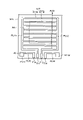
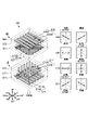
- FIG. 1 shows a perspective view of a liquid crystal light control device 100 according to one embodiment of the present invention.
- the liquid crystal light control device 100 includes a liquid crystal light control element 102 and a circuit board 104 .
- Liquid crystal light control element 102 includes a plurality of liquid crystal cells.
- the liquid crystal light control element 102 is preferably composed of a plurality of liquid crystal cells, such as two liquid crystal cells or four liquid crystal cells.
- FIG. 1 shows an example in which the liquid crystal light control element 102 is composed of a first liquid crystal cell 10, a second liquid crystal cell 20, a third liquid crystal cell 30, and a fourth liquid crystal cell 40.
- the first liquid crystal cell 10, the second liquid crystal cell 20, the third liquid crystal cell 30, and the fourth liquid crystal cell 40 are flat panels, and are arranged so that the flat surfaces of the respective liquid crystal cells overlap.
- Transparent adhesive layers are provided between the first liquid crystal cell 10 and the second liquid crystal cell 20, between the second liquid crystal cell 20 and the third liquid crystal cell 30, and between the third liquid crystal cell 30 and the fourth liquid crystal cell 40.
- the liquid crystal light control element 102 has a structure in which liquid crystal cells arranged adjacent to each other in the front and rear are adhered with a transparent adhesive layer.
- the circuit board 104 includes circuits for driving the liquid crystal light control element 102 .
- the first liquid crystal cell 10 is connected to the circuit board 104 through the first flexible wiring board F1
- the second liquid crystal cell 20 is connected to the circuit board 104 through the second flexible wiring board F2
- the third liquid crystal cell 30 is connected to the third flexible wiring.
- the substrate F3 is connected to the circuit board 104
- the fourth liquid crystal cell 40 is connected to the circuit board 104 by the fourth flexible wiring board F4.
- the circuit board 104 outputs a control signal for controlling the alignment state of the liquid crystal to each liquid crystal cell through the flexible wiring board.
- the liquid crystal light control device 100 is configured such that the light emitted from the light source section 106 is emitted to the front side of the drawing through the liquid crystal light control element 102 .
- the first liquid crystal cell 10 the second liquid crystal cell 20, the third liquid crystal cell 30, and the fourth liquid crystal cell 40 are arranged in this order from the light source section 106 side.
- the light source unit 106 includes a white light source, and an optical element such as a lens may be arranged between the white light source and the liquid crystal light control element 102 as necessary.
- the white light source is a light source that emits light close to natural light, and may emit dimmed light such as daylight white or incandescent light.
- the light source unit 106 is desirably composed of a light source having a narrow light distribution range.
- the liquid crystal light control device 100 has a function of controlling the diffusion direction of light emitted from the light source section 106 by means of the liquid crystal light control element 102 .
- the liquid crystal light control element 102 can make the light emitted from the light source section 106 into a predetermined light distribution pattern such as a square shape or a line shape.
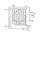
- FIG. 2 shows a developed view of the liquid crystal light control element 102 shown in FIG.
- the liquid crystal light control element 102 shows an example including a first liquid crystal cell 10 , a second liquid crystal cell 20 , a third liquid crystal cell 30 and a fourth liquid crystal cell 40 .
- the liquid crystal light control element 102 is not limited to the illustrated configuration, and may be composed of two liquid crystal cells, the first liquid crystal cell 10 and the second liquid crystal cell 20, for example.
- the first liquid crystal cell 10 includes a first substrate S11 and a second substrate S12.
- the first substrate S11 and the second substrate S12 face each other and are arranged with a gap therebetween.
- a liquid crystal layer (not shown) is provided in the gap between the first substrate S11 and the second substrate S12.
- the first flexible wiring board F1 is connected to connection terminals provided on the first board S11, for example.
- the second liquid crystal cell 20 includes a first substrate S21, a second substrate S22, and a second flexible wiring substrate F2, and has the same configuration as the first liquid crystal cell 10.
- the third liquid crystal cell 30 includes a first substrate S31, a second substrate S32, and a third flexible wiring substrate F3, and has the same configuration as the first liquid crystal cell 10.
- FIG. The fourth liquid crystal cell 40 includes a first substrate S41, a second substrate S42, and a fourth flexible wiring substrate F4, and has the same configuration as the first liquid crystal cell 10.
- a first transparent adhesive layer TA1 is provided between the first liquid crystal cell 10 and the second liquid crystal cell 20.
- the first transparent adhesive layer TA1 transmits visible light and is provided to bond the second substrate S12 of the first liquid crystal cell 10 and the first substrate S21 of the second liquid crystal cell 20 together.
- a second transparent adhesive layer TA2 is provided between the second liquid crystal cell 20 and the third liquid crystal cell 30 .
- the second transparent adhesive layer TA2 transmits visible light and is provided to bond the second substrate S22 of the second liquid crystal cell 20 and the first substrate S31 of the third liquid crystal cell 30 together.
- a third transparent adhesive layer TA3 is provided between the third liquid crystal cell 30 and the fourth liquid crystal cell 40 .
- the third transparent adhesive layer TA3 transmits visible light and is provided to bond the second substrate S32 of the third liquid crystal cell 30 and the first substrate S41 of the fourth liquid crystal cell 40 together.
- the first transparent adhesive layer TA1, the second transparent adhesive layer TA2, and the third transparent adhesive layer TA3 have a high transmittance, and have refractive indices of the first substrates S11, S21, S31, S41 and the second substrates S12, S22, S23, A value close to S24 is preferable.
- an optical elastic resin can be used. can be done.
- the thermal expansion coefficients of the first transparent adhesive layer TA1, the second transparent adhesive layer TA2, and the third transparent adhesive layer TA3 are It preferably has a value close to the thermal expansion coefficients of the first substrate and the second substrate.
- the first liquid crystal cell 10, the second liquid crystal cell 20, the third liquid crystal cell 30, and the fourth liquid crystal cell 40 have substantially the same structure except for the configuration of the electrodes.
- the liquid crystal light control element 102 according to this embodiment is arranged so that the electrodes of the first liquid crystal cell 10 on the first substrate S11 side and the electrodes of the substrates of the third liquid crystal cell 30 on the first substrate S31 side intersect.
- the patterns of the corresponding electrodes of the first liquid crystal cell 10 and the third liquid crystal cell 30 may be formed so as to cross each other, or as shown in FIG. 30 may be rotated by a predetermined angle (90 degrees in this embodiment).
- Each liquid crystal cell that constitutes the liquid crystal light control element 102 has strip-shaped electrodes arranged side by side on the main surface of the substrate, and the strip-shaped electrodes generate a lateral electric field.
- the strip-shaped electrodes are not oriented in the same direction in all the liquid crystal cells, but in the range of 0 degrees to 180 degrees for the first substrate and the second substrate of each liquid crystal cell when a certain direction is 0 degrees. placed in a tilted (rotated) state.
- the liquid crystal light control element 102 according to the present embodiment can suppress the occurrence of moire and non-uniformity in brightness (color unevenness) by devising the arrangement of the electrode patterns of the liquid crystal cells. The details are described below.
- FIG. 3 is a development view schematically showing the arrangement of electrodes provided in each of the first liquid crystal cell 10, the second liquid crystal cell 20, the third liquid crystal cell 30, and the fourth liquid crystal cell 40.
- FIG. FIG. 3 shows the electrode arrangement of the first liquid crystal cell 10, the second liquid crystal cell 20, the third liquid crystal cell 30, and the fourth liquid crystal cell 40 in order from the bottom.
- FIG. 3 shows the strip-shaped electrodes provided on the first substrate and the second substrate of each liquid crystal cell viewed from the second substrate side.
- the first liquid crystal cell 10 has a first electrode E11 provided on the first substrate S11 and a second electrode E12 provided on the second substrate S12.
- the first electrode E11 includes a plurality of first strip-shaped electrodes E11A and second strip-shaped electrodes E11B formed in strips. The first strip electrodes E11A and the second strip electrodes E11B are alternately arranged.
- the second electrode E12 includes a plurality of third strip-shaped electrodes E12A and fourth strip-shaped electrodes E12B formed in strips. The third strip-shaped electrodes E12A and the fourth strip-shaped electrodes E12B are alternately arranged.
- the first substrate S11 and the second substrate S12 are arranged to face each other, and it is also possible to define the facing surface as the inner surface and the surface opposite to the inner surface as the outer surface.
- the first electrode E11 is provided on the inner surface of the first substrate S11
- the second electrode E12 is provided on the inner surface of the second substrate S12.
- the second liquid crystal cell 20 the third liquid crystal cell 30, and the fourth liquid crystal cell 40 described below.
- the second liquid crystal cell 20 has a first electrode E21 and a second electrode E22
- the third liquid crystal cell 30 has a first electrode E31 and a second electrode E32
- the fourth liquid crystal cell 40 has a first electrode E41 and a second electrode E32. It has two electrodes E42.
- the first electrodes E21, E31, E41 and the second electrodes E22, E32, E42 each have a plurality of strip-shaped electrodes.
- the longitudinal direction of the first electrode E11 of the first liquid crystal cell 10 (longitudinal direction of the first strip-shaped electrode E11A and the second strip-shaped electrode E11B) is parallel to 90 to 270 degrees (90 degrees to 270 degrees in the figure). The same applies hereinafter), and the longitudinal direction of the second electrode E21 (longitudinal direction of the third strip electrode E12A and the fourth strip electrode E12B) is arranged in a direction parallel to 45 to 225 degrees.
- the longitudinal direction of the first electrode E21 is arranged in a direction parallel to 135-315 degrees
- the second electrode E21 is arranged in a direction parallel to 90-270 degrees
- the third liquid crystal The cell 30 has the first electrode E31 arranged in a direction parallel to 0-180 degrees
- the second electrode E32 arranged in a direction parallel to 135-315
- the fourth liquid crystal cell 40 has the first electrode E41 arranged in a direction parallel to 45 degrees. They are arranged in a direction parallel to -225 degrees
- the second electrodes E42 are arranged in a direction parallel to 0-180 degrees.
- the first electrode E11 of the first liquid crystal cell 10 and the first electrode E31 of the third liquid crystal cell 30 are arranged to E12 is arranged to intersect the second electrode E32 of the third liquid crystal cell 30.
- the first electrode E21 of the second liquid crystal cell 20 is arranged to cross the first electrode E41 of the fourth liquid crystal cell 40
- the second electrode E22 is arranged to cross the second electrode E42 of the fourth liquid crystal cell 40.
- Alignment films provided on each substrate are omitted in FIG. 3, but the alignment directions of the alignment films are indicated by arrows.
- the alignment direction ALD11 of the alignment film of the first substrate S11 of the first liquid crystal cell 10 is oriented in a direction crossing the longitudinal direction of the first electrode E11, that is, oriented in a direction of 0-180 degrees.
- the alignment direction ALD12 of the alignment film of the two substrates S12 is oriented in a direction crossing the longitudinal direction of the second electrode E12, that is, oriented in a direction parallel to 135-315 degrees.
- the same applies to the second liquid crystal cell 20, the third liquid crystal cell 30, and the fourth liquid crystal cell 40, and the alignment direction of the alignment film provided on each substrate is oriented in a direction intersecting the longitudinal direction of each electrode. .
- the angle at which each orientation direction intersects with the electrode can be set within a range of 90° ⁇ 10°.
- a liquid crystal layer is provided between the first substrate and the second substrate of each liquid crystal cell.
- the initial alignment state of the liquid crystal layer is determined by the alignment direction of the alignment film, and the alignment state of the liquid crystal molecules is controlled by the voltage applied to the first electrode and the second electrode.
- the first liquid crystal cell 10, the second liquid crystal cell 20, the third liquid crystal cell 30, and the fourth liquid crystal cell 40 have substantially the same configuration except that the arrangement of the electrodes and the alignment direction of the alignment film are different. ing.
- the first liquid crystal cell 10 will be described in more detail as a representative.
- FIG. 4A shows a plan view of the first substrate S11
- FIG. 4B shows a plan view of the second substrate S12. More specifically, FIG. 4A shows a plan view of the inner surface of the first substrate S11, and FIG. 4B shows a plan view of the inner surface of the second substrate S12.
- a first electrode E11 is provided on a first substrate S11.
- the first electrode E11 includes a plurality of first strip electrodes E11A and a plurality of second strip electrodes E11B.
- the plurality of first strip-shaped electrodes E11A and the plurality of second strip-shaped electrodes E11B have strip-shaped patterns.
- the strip-shaped patterns of the plurality of first strip-shaped electrodes E11A and the strip-shaped patterns of the plurality of second strip-shaped electrodes E11B are alternately arranged at predetermined intervals in a direction crossing the longitudinal direction.
- the plurality of first strip electrodes E11A are each connected to a first feed line PL11, and the plurality of second strip electrodes E11B are each connected to a second feed line PL12.
- the first power supply line PL11 is connected to the first connection terminal T11
- the second power supply line PL12 is connected to the second connection terminal T12.
- the first connection terminal T11 and the second connection terminal T12 are provided along one edge of the first substrate S11.
- the first substrate S11 is provided with a third connection terminal T13 adjacent to the first connection terminal T11 and a fourth connection terminal T14 adjacent to the second connection terminal T12.
- the third connection terminal T13 is connected to the fifth power supply line PL15.
- the fifth power supply line PL15 is connected to a first power supply terminal PT11 provided at a predetermined position on the surface of the first substrate S11.
- the fourth connection terminal T14 is connected to the sixth power supply line PL16.
- the sixth power supply line PL16 is connected to a second power supply terminal PT12 provided at a predetermined position in the plane of the first substrate S11.
- the same voltage is applied to the plurality of first strip electrodes E11A by being connected to the first feed line PL11.
- the same voltage is applied to the plurality of second strip-shaped electrodes E11B by being connected to the second feed line PL12.
- the plurality of first strip electrodes E11A and the plurality of second strip electrodes E11B are alternately arranged.
- the plurality of first strip electrodes E11A and the plurality of second strip electrodes E11B are electrically separated.
- a second electrode E12 is provided on the second substrate S12.
- the second electrode E12 includes a plurality of third strip electrodes E12A and a plurality of fourth strip electrodes E12B.
- the plurality of third strip-shaped electrodes E12A and the plurality of fourth strip-shaped electrodes E12B have strip-shaped patterns.
- the strip patterns of the plurality of third strip electrodes E12A and the strip patterns of the plurality of fourth strip electrodes E12B are alternately arranged at predetermined intervals in a direction crossing the longitudinal direction.
- the plurality of third strip-shaped electrodes E12A and the plurality of fourth strip-shaped electrodes E12B are arranged at an angle of 45 degrees with respect to the longitudinal direction of the plurality of first strip-shaped electrodes E11A and the plurality of second strip-shaped electrodes E11B.
- the angle at which the plurality of third strip-shaped electrodes E12A and the plurality of fourth strip-shaped electrodes E12B intersect with the plurality of first strip-shaped electrodes E11A and the plurality of second strip-shaped electrodes E11B is set within a range of 45° ⁇ 10°. It is possible.
- the plurality of third strip electrodes E12A are each connected to a third feed line PL13, and the plurality of fourth strip electrodes E12B are each connected to a fourth feed line PL14.
- the third power supply line PL13 is connected to the third power supply terminal PT13, and the fourth power supply line PL14 is connected to the fourth power supply terminal PT14.
- the third power supply terminal PT13 is provided at a position corresponding to the first power supply terminal PT11 of the first substrate S11, and the fourth power supply terminal PT14 is provided at a position corresponding to the second power supply terminal PT12 of the first substrate S11.
- the same voltage is applied to the plurality of third strip electrodes E12A by being connected to the third feed line PL13.
- the same voltage is applied to the plurality of fourth strip-shaped electrodes E12B by being connected to the fourth feed line PL14.
- the plurality of third strip electrodes E12A and the plurality of fourth strip electrodes E12B are alternately arranged.
- the plurality of third strip electrodes E12A and the plurality of fourth strip electrodes E12B are electrically separated.
- a first connection terminal T11, a second connection terminal T12, a third connection terminal 13, and a fourth connection terminal T14 provided on the first substrate S11 are terminals connected to the flexible wiring substrate.
- the first power supply terminal PT11 and the third power supply terminal PT13 are electrically connected by a conductive material
- the second power supply terminal PT12 and the fourth power supply terminal PT14 are electrically connected to the conductive material. connected to
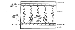
- FIG. 5 shows a cross-sectional view of the first liquid crystal cell 10.
- FIG. The cross-sectional structure of the first liquid crystal cell 10 shown in FIG. 5 shows the cross-sectional structure corresponding to the A1-A2 line of the first substrate S11 shown in FIG. 4A and the second substrate S12 shown in FIG. 4B.
- the first liquid crystal cell 10 has an effective area AA capable of polarizing and scattering (diffusing) incident light.
- the first electrode E11 and the second electrode E12 are arranged within the effective area AA.
- the first substrate S11 and the second substrate S12 are bonded together by a sealing material SE provided outside the effective area AA.
- a gap for sealing the first liquid crystal layer LC1 is provided between the first substrate S11 and the second substrate S12.
- the first liquid crystal layer LC1 is enclosed between the first substrate S11 and the second substrate S12 with a sealing material SE.
- the first substrate S11 has a first electrode E11 and a first power supply terminal PT11, and has a structure in which a first alignment film AL11 is provided on the first electrode E11.
- the first electrode E11 includes a first strip-shaped electrode E11A and a second strip-shaped electrode E11B.
- the first power supply terminal PT11 has a structure continuous from the fifth power supply line PL15, and is arranged outside the sealing material SE.
- the second substrate S12 has a second electrode E12 and a third power supply terminal PT13, and has a structure in which a second alignment film AL12 is provided on the second electrode E12.
- the second electrode E12 includes a third strip-shaped electrode E12A and a fourth strip-shaped electrode E12B.
- the third power supply terminal PT13 has a structure continuous from the third power supply line PL13, and is arranged outside the sealing material SE.
- the first electrode E11 and the second electrode E12 are provided so that the longitudinal direction of the strip-shaped electrode pattern intersects. That is, the longitudinal direction of the first strip-shaped electrode E11A and the second strip-shaped electrode E11B is arranged so as to cross the longitudinal direction of the third strip-shaped electrode E12A and the fourth strip-shaped electrode E12B.
- the first strip-shaped electrode E11A and the second strip-shaped electrode E11B, and the third strip-shaped electrode E12A and the fourth strip-shaped electrode E12B intersect at an angle of approximately 45 degrees in this embodiment.
- the crossing angle between the first electrode E11 and the second electrode E12 can be set, for example, within a range of 45 degrees ⁇ 10 degrees.
- first electrode E11 and the second electrode E12 By arranging the first electrode E11 and the second electrode E12 not only along the X-axis direction and the Y-axis direction, but also in directions rotated within a range of 45° ⁇ 10°, variations in electrode arrangement can be achieved. Even when the liquid crystal light control element 102 has a plurality of liquid crystal cells stacked, interference can be prevented by preventing liquid crystal cells having the same electrode arrangement from overlapping, and moire can be suppressed.
- the first power supply terminal PT11 and the third power supply terminal PT13 are arranged so as to face each other in a region outside the seal material SE.
- the first conductive member CP11 is arranged between the first power supply terminal PT11 and the third power supply terminal PT13 to electrically connect them.
- the first conductive member CP11 can be made of a conductive paste material, such as silver paste or carbon paste.
- the second power supply terminal PT12 and the fourth power supply terminal PT14 are similarly electrically connected by a conductive member.
- the first substrate S11 and the second substrate S12 are translucent substrates, such as glass substrates and resin substrates.
- the first electrode E11 and the second electrode E12 are transparent electrodes made of a transparent conductive material such as indium tin oxide (ITO) or indium zinc oxide (IZO).
- power supply lines (first power supply line PL11, second power supply line PL12, third power supply line PL13, fourth power supply line PL14, fifth power supply line PL15, sixth power supply line PL16), connection terminals (first connection terminal T11, 2 connection terminal T12, third connection terminal T13, fourth connection terminal T14) and power supply terminals (first power supply terminal PT11, second power supply terminal PT12, third power supply terminal PT13, fourth power supply terminal PT14) are made of aluminum, It is made of metal materials such as titanium, molybdenum, and tungsten.
- the feeder lines (first feeder line PL11, second feeder line PL12, third feeder line PL13, fourth feeder line PL14, fifth feeder line PL15, sixth feeder line PL16) are connected to the first electrode E11 and the second feeder line PL16. It may be formed of the same transparent conductive film as the electrode E12.
- the alignment films AL1 and AL2 are formed of horizontal alignment films having an alignment control force substantially parallel to the main plane of the substrate.
- first liquid crystal layer LC1 for example, twisted nematic liquid crystal (TN (Twisted Nematic) liquid crystal
- TN Transmission Nematic liquid crystal
- a spacer may be provided between the first substrate S11 and the second substrate S12 to keep the distance between the two substrates constant.
- FIG. 4 shows a pattern in which the third strip-shaped electrodes E12A and the fourth strip-shaped electrodes E12B on the second substrate S12 side are arranged obliquely on the substrate.
- a liquid crystal cell may be configured by using the first substrate S11 and the second substrate S12 formed so as to match each other, rotating one of the substrates by a predetermined angle, and bonding them together.
- 7A and 7B show a partial schematic cross-sectional structure of the first liquid crystal cell 10, showing elements necessary for explanation.
- 7A and 7B show a first strip-shaped electrode E11A, a second strip-shaped electrode E11B, a first alignment film AL11 provided on the first substrate S11, a second alignment film AL12 provided on the second substrate S12, and a first alignment film AL12.
- a liquid crystal layer LC1 is shown.
- the third strip-shaped electrode E12A and the fourth strip-shaped electrode E12B are omitted to simplify the explanation.
- FIG. 7A shows that the alignment direction of the first alignment film AL11 and the alignment direction of the second alignment film AL12 are different.
- the first alignment film AL11 is subjected to alignment treatment in an alignment direction ALD1 that intersects the longitudinal direction of the first strip-shaped electrode E11A and the second strip-shaped electrode E11B at an angle of 90 degrees.
- the second alignment film AL12 is oriented in an alignment direction ALD2 that intersects the longitudinal direction of the third strip-shaped electrode E12A and the fourth strip-shaped electrode E12B at an angle of 90 degrees. Therefore, the alignment direction of the first alignment film AL11 and the alignment direction of the second alignment film AL12 of the first liquid crystal cell 10 shown in FIGS.
- the alignment treatment may be a rubbing treatment or an optical alignment treatment.
- the orientation direction of the orientation film can be set within a range of 90° ⁇ 10° with respect to the extending direction of the strip electrodes.
- FIG. 7A shows a state in which no voltage is applied to the first strip-shaped electrode E11A and the second strip-shaped electrode E11B, and a state in which the long axis direction of the liquid crystal molecules is twisted by 45 degrees.
- FIG. 7A shows an example in which the first liquid crystal layer LC1 is formed of positive twisted nematic liquid crystal (TN liquid crystal) and the long axis of the liquid crystal molecules is aligned in the same direction as the alignment direction of the alignment film.
- TN liquid crystal positive twisted nematic liquid crystal
- the liquid crystal preferably contains a chiral agent that imparts twist to liquid crystal molecules.
- FIG. 7B shows a state in which a low-level voltage VL is applied to the first strip-shaped electrode E11A and a high-level voltage VH is applied to the second strip-shaped electrode E11B.
- a horizontal electric field is generated between the first strip-shaped electrode E11A and the second strip-shaped electrode E11B.
- the orientation direction of the liquid crystal molecules on the first substrate S11 side changes under the influence of the lateral electric field.
- the orientation of the liquid crystal molecules on the first substrate S11 side changes such that the long axis direction is parallel to the direction of the electric field.
- the values of the low-level voltage VL and the high-level voltage VH applied to the first strip-shaped electrode E11A and the second strip-shaped electrode E11B are appropriately set. For example, 0 V is applied as the low-level voltage VL1, and a voltage of 5 to 30 V is applied as the high-level voltage VH1. A voltage in which a low-level voltage VL and a high-level voltage VH are alternately applied is applied to the first strip-shaped electrode E11A and the second strip-shaped electrode E11B. For example, as shown in FIG. 7C, during a given period, a low-level voltage VL is applied to the first strip-shaped electrode E11A and a high-level voltage VH is applied to the second strip-shaped electrode E11B. A high-level voltage VH is applied to the first strip-shaped electrode E11A and a low-level voltage VL is applied to the second strip-shaped electrode E11B. A voltage may be applied.
- the frequency of the voltage applied to the first strip-shaped electrode E11A and the second strip-shaped electrode E11B may be any frequency that allows the liquid crystal molecules to follow changes in the electric field, for example, 15 to 100 Hz.
- FIG. 8A is a partial perspective view of the first liquid crystal cell 10, showing the arrangement of the first and second strip electrodes E11A and E11B, the third and fourth strip electrodes E12A and E12B, and the first liquid crystal layer LC1.
- indicates 8B and 8C show schematic cross-sectional views of the first liquid crystal cell 10.
- FIG. 8B shows a schematic cross-sectional view of the first liquid crystal cell 10 shown in FIG. 8A when viewed from side A shown in the drawing
- FIG. 8C shows a schematic cross-sectional view when viewed from side B shown in the drawing.
- 8B and 8C show that the orientation treatment direction of the first orientation film AL11 and the orientation treatment direction of the second orientation film AL12 are different.
- the first strip-shaped electrode E11A and the second strip-shaped electrode E11B are arranged with a center-to-center distance W
- first strip-shaped electrode E11A and the second strip-shaped electrode E11B are separated from the third strip-shaped electrode E12A and the fourth strip-shaped electrode E12B, and are arranged to face each other while intersecting each other at an angle of 45° ⁇ 10°.
- the first substrate S11 and the second substrate S12 are arranged facing each other with a distance D, and the distance D substantially corresponds to the thickness of the first liquid crystal layer LC1.
- a first strip-shaped electrode E11A and a first alignment film AL11 are provided on the first substrate S11
- a third strip-shaped electrode E12A and a second alignment film AL12 are provided on the second substrate S12.
- the thickness of the first liquid crystal layer LC1 can be regarded as the gap D.
- the distance D between the strip electrodes sandwiching the first liquid crystal layer LC1 is preferably equal to or larger than the distance W between the centers of the strip electrodes. That is, it is preferable that the interval D has a length equal to or longer than the center-to-center distance W. For example, the distance D is preferably twice or more the distance W between the centers of the strip electrodes.
- the width of the first strip-shaped electrode E11A is 5 ⁇ m
- the width a of the first strip-shaped electrode E11A and the second strip-shaped electrode E11B is 5 ⁇ m
- the distance from the end of the first strip-shaped electrode E11A to the end of the second strip-shaped electrode E11B is
- the interval b is 5 ⁇ m
- the center-to-center distance W of the strip electrodes is 10 ⁇ m.
- the interval D has a size of 10 ⁇ m or more.
- the electric field generated by the first strip electrode E11A and the second strip electrode E11B and the third strip electrode E12A and the fourth strip electrode E12A Mutual interference with the electric field generated by the electrode E12B can be suppressed as much as possible. That is, as shown in FIG. 8B, when the electric field between the first strip-shaped electrode E11A and the second strip-shaped electrode E11B changes the orientation of the liquid crystal molecules in the vicinity thereof, the electric field between the third strip-shaped electrode E12A and the fourth strip-shaped electrode E12B Even if an electric field is generated at , there is almost no effect because the distance D is sufficiently large. Moreover, as shown in FIG. 8C, the same applies to the case where an electric field is generated between the third strip-shaped electrode E12A and the fourth strip-shaped electrode E12B.
- the refractive index of liquid crystals changes depending on the alignment state.
- the long axis direction of the liquid crystal molecules is aligned horizontally with the surface of the substrate, and the liquid crystal molecules are aligned from the first substrate S11 side to the first substrate S11 side.
- the two substrates S12 are oriented in a twisted state of 45 degrees.
- the first liquid crystal layer LC1 has a substantially uniform refractive index distribution in this alignment state.
- the first polarization component PL1 of the light incident on the first liquid crystal cell 10 and the second polarization component PL2 orthogonal to the first polarization component PL1 are optically rotated under the influence of the initial orientation of the liquid crystal molecules, but are mostly refracted. It passes through the first liquid crystal layer LC1 without being (or scattered).
- the first polarization component PL1 corresponds to, for example, P-polarization of natural light
- the second polarization component corresponds to, for example, S-polarization.
- the first liquid crystal layer LC1 in the ON state in which a voltage is applied to the first strip-shaped electrode E11A and the second strip-shaped electrode E11B to form an electric field, the first liquid crystal layer LC1 has positive dielectric anisotropy. , the liquid crystal molecules align with their long axes along the electric field. As a result, as shown in FIG. 7B, the first liquid crystal layer LC1 has a region in which the liquid crystal molecules rise substantially vertically above the first strip-shaped electrode E11A and the second strip-shaped electrode E11B. A region that is obliquely oriented along the distribution of the electric field between the strip electrode E11B and a region that maintains the initial alignment state in a region apart from the first strip electrode E11A and the second strip electrode E11B are formed.
- the long axes of the liquid crystal molecules are aligned in a convex circular arc along the direction in which the electric field is generated. That is, as shown in FIGS. 7A and 7B, the direction of the initial alignment of the liquid crystal molecules is the same as the direction of the lateral electric field generated between the first strip-shaped electrode E11A and the second strip-shaped electrode E11B. As shown in the diagram, the alignment direction of the liquid crystal molecules positioned substantially in the center between the two electrodes is almost unchanged, but the liquid crystal molecules positioned on the respective electrode sides from the central portion follow the intensity distribution of the electric field to the first substrate.
- an arc-shaped refractive index distribution (permittivity distribution) is formed in the first liquid crystal layer LC1 under the influence of the horizontal electric field generated by the first strip-shaped electrode E11A and the second strip-shaped electrode E11B.
- the polarized component parallel to the initial orientation direction of the liquid crystal molecules is radially diffused.
- an arcuate refractive index distribution is formed in the first liquid crystal layer LC1 under the influence of the horizontal electric field by the third strip-shaped electrode E12A and the fourth strip-shaped electrode E12B.
- the polarized component parallel to the initial orientation direction of the liquid crystal molecules is radially diffused.
- Liquid crystal molecules have a refractive index anisotropy ⁇ n. Therefore, the first liquid crystal layer LC1 in the ON state has a refractive index distribution or a retardation distribution according to the alignment state of the liquid crystal molecules.
- the retardation here is represented by ⁇ n ⁇ d, where d is the thickness of the first liquid crystal layer LC1.
- the polarized light component parallel to the long axis direction of the liquid crystal molecules is scattered by the refractive index distribution of the first liquid crystal layer LC1 when passing through the first liquid crystal layer LC1. (spread).
- a liquid crystal layer having positive liquid crystal molecules is used.
- FIG. 9 schematically shows a phenomenon in which the first polarization component PL1 and the second polarization component PL2 incident on the first liquid crystal cell 10 are diffused by the first liquid crystal layer LC1.
- the directions of 0 degrees, 45 degrees, 90 degrees, 135 degrees, 180 degrees, 225 degrees, 270 degrees, and 315 degrees are shown as having the relationship shown in the legend.
- the X-axis direction is the same as the 0-180 degree direction
- the Y-axis direction is the same as the 90-270 degree direction.
- the 45-225 degree direction refers to the direction along the line segment that bisects the intersection angle when the X-axis and the Y-axis are perpendicular to each other.
- the X-axis direction may be indicated as 0-180 degree direction, and the Y-axis direction as 90-270 degree direction.
- the rotation angle is shown counterclockwise with the X axis being 0 degrees, and the directions corresponding to the rotation angles are shown as 45-225 direction and 90-270 direction (Y-axis direction).
- the relationship between the direction of each axis and the angle shown in FIG. 9 and the relationship between angles in the drawing showing the direction of the polarization axis of each polarization component on the right side of FIG. 9 are the same for FIGS.
- the left column shows the electrode arrangement of the first liquid crystal cell 10, the alignment direction of the alignment film, and the direction of the long axis of the liquid crystal molecules, and each direction is based on the direction shown in the legend.
- the longitudinal direction of the first strip-shaped electrode E11A and the second strip-shaped electrode E11B is arranged in the Y-axis direction (direction of 90-270 degrees), and the longitudinal direction of the third strip-shaped electrode E12A and the fourth strip-shaped electrode E12B is arranged. is rotated clockwise (45 to 225 degrees) within a range of 45 degrees ⁇ 10 degrees with respect to the Y-axis direction.
- the alignment direction of the alignment film on the first substrate S11 side is in the X direction
- the alignment direction of the alignment film on the second substrate S12 side is the direction rotated clockwise by 45 degrees (135-315 degrees) from the X-axis direction. direction).
- the polarization axis of the first polarization component PL1 is in the Y-axis direction
- the polarization axis of the second polarization component PL2 is in the X-axis direction.
- a potential difference is generated between the first strip-shaped electrode E11A and the second strip-shaped electrode E11B, and an electric field is generated between them.
- a potential difference is also generated between the third strip-shaped electrode E12A and the fourth strip-shaped electrode E12B, and an electric field is generated between them.
- the right column of FIG. 9 shows the polarization directions of the first polarization component PL1 and the second polarization component PL2 by applying them to the angles shown in the legend. Focusing on the first polarization component PL1 in FIG. 9, the polarization direction of the first polarization component PL1 incident on the first liquid crystal cell 10 is in the long axis direction of the liquid crystal molecules on the first substrate S11 side of the first liquid crystal layer LC1. It is in the direction that intersects (perpendicularly). Therefore, although the liquid crystal molecules on the first substrate S11 side change the refractive index distribution due to the electric field generated by the first electrode E11, the first polarized light component PL1 is not diffused and goes straight to the second substrate S12 side.
- the first polarized light component PL1 is optically rotated by 45 degrees according to the twisted orientation of the liquid crystal molecules in the process of moving the first liquid crystal layer LC1 from the first substrate S11 side to the second substrate S12 side. Since the polarization axis of the first polarization component PL1 after optical rotation is in the direction of 45-225 degrees, it is in the direction crossing the major axis direction of the liquid crystal molecules on the second substrate S12 side. Therefore, although the liquid crystal molecules on the second substrate S12 side change the refractive index distribution by the electric field generated by the second electrode E12, the second polarization component PL2 is not affected by the electric field and is transmitted as it is. Thus, the first polarized light component PL1 is optically rotated by 45 degrees while passing through the first liquid crystal cell 10, but passes through the first liquid crystal cell 10 without being diffused or the like.
- the polarization direction of the second polarization component PL2 is parallel to the long axis direction of the liquid crystal molecules on the first substrate S11 side of the first liquid crystal layer LC1. Therefore, the liquid crystal molecules on the first substrate S11 side have a refractive index distribution due to the electric field generated by the first electrode E11, and the second polarization component PL2 is diffused by this action.
- the second polarization component PL2 is rotated by 45 degrees according to the twisted orientation of the liquid crystal molecules in the process of moving the first liquid crystal layer LC1 from the first substrate S11 side to the second substrate S12 side.
- the polarization axis of the second polarization component PL2 is in the direction rotated clockwise by 45 degrees (direction of 135-315 degrees), so that it is in the direction parallel to the major axis direction of the liquid crystal molecules on the second substrate S12 side. Since the liquid crystal molecules on the second substrate S12 side change the refractive index distribution by the electric field generated by the second electrode E12, the first polarization component PL1 transitioned by the first liquid crystal layer LC1 is the liquid crystal on the second substrate S12 side. It is diffused in the direction of 135-315 degrees by the refractive index profile formed by the molecules.
- the second polarization component PL2 incident on the first liquid crystal cell 10 is optically rotated by 45 degrees in the process of passing through the first liquid crystal cell 10, and is polarized in the X direction (direction of 0-180 degrees) and the direction of 135-315 degrees.
- FIG. 10 shows the relationship between the arrangement of strip electrodes in each liquid crystal cell of the liquid crystal light control element 102 according to the first embodiment and the diffused polarized light component.
- the liquid crystal light control element 102 has a structure in which a first liquid crystal cell 10, a second liquid crystal cell 20, a third liquid crystal cell 30, and a fourth liquid crystal cell 40 are stacked from the light incident side.
- the left column shows the electrode arrangement of the first liquid crystal cell 10, the second liquid crystal cell 20, the third liquid crystal cell 30, and the fourth liquid crystal cell 40, the alignment direction of the alignment film, and the direction of the long axis of the liquid crystal molecules.
- the polarization directions of the first polarization component PL1 and the second polarization component PL2 are shown by applying the angles shown in the legend as in FIG.
- the first polarized light component PL1 and the second polarized light component PL2 orthogonal to the first polarized light component PL1 of the incident light enter the first liquid crystal cell 10 and exit from the fourth liquid crystal cell 40. Since the light is optically rotated in the layers, the optical rotation states of the first polarization component PL1 and the second polarization component PL2 in each liquid crystal cell are indicated by arrows in the right column of FIG.
- Such display is the same for FIGS. 11 to 14 as well.
- the arrangement of the first electrodes and the arrangement of the second electrodes of each liquid crystal cell are all different.
- the longitudinal direction of the first strip-shaped electrode E11A and the second strip-shaped electrode E11B of the first liquid crystal cell 10 (also referred to as the “longitudinal direction of the first electrode E11” in the following description) is oriented 90 to 270 degrees.
- the third strip-shaped electrode E12A and the fourth strip-shaped electrode E12B (also referred to as "longitudinal direction of the second electrode E12" in the following description) are oriented in the direction of 45-225 degrees.
- the orientation direction of the orientation film (not shown) is provided in a direction intersecting the longitudinal direction of the strip electrodes, the orientation direction of the orientation film on the first substrate S11 side is in the direction of 0 to 180 degrees, and the orientation direction on the second substrate S12 side is 0 to 180 degrees.
- the alignment direction of the alignment film is in the direction of 135-315 degrees. That is, in the first liquid crystal cell 10, the second electrode E12 is arranged to intersect the first electrode E11 at an angle within the range of 45° ⁇ 10° (45° in this embodiment). Alignment directions are also provided so that the first substrate S11 side and the second substrate S12 side intersect at an angle of 45 degrees.
- the longitudinal direction of the first electrode E11 is oriented in the direction of 135-315 degrees
- the longitudinal direction of the second electrode E22 is oriented in the direction of 90-270 degrees
- the first substrate S21 side is directed to the direction of 0-180 degrees.
- the longitudinal direction of the first electrode E31 is oriented in the direction of 0-180 degrees
- the longitudinal direction of the second electrode E32 is oriented in the direction of 135-315 degrees
- the first substrate S31 side is oriented in the direction of 45-225 degrees.
- the longitudinal direction of the first electrode E41 is oriented in the direction of 45-225 degrees
- the longitudinal direction of the second electrode E42 is oriented in the direction of 90-270 degrees
- the first substrate S41 side is directed to the 0-180 degree direction.
- the longitudinal direction of the second electrode E12 of the first liquid crystal cell 10 and the longitudinal direction of the first electrode E21 of the second liquid crystal cell 20 and the longitudinal direction of the third liquid crystal cell 30 The longitudinal direction of the first electrode E31, and the longitudinal direction of the second electrode E32 of the third liquid crystal cell 30 and the longitudinal direction of the first electrode E41 of the fourth liquid crystal cell 40 form an angle of 90° ⁇ 10° (this embodiment 90 degrees in the form).
- the longitudinal direction of the liquid crystal molecules on the first substrate S11 side is oriented in the direction of 0-180 degrees
- the longitudinal direction of the liquid crystal molecules on the second substrate S12 side is oriented in the direction of 135-315 degrees.
- the parallel polarization component (PL 0/180 ) in the direction of 0-180 degrees is affected by the arc-shaped refractive index distribution of the first liquid crystal layer LC1, and The directionally diffuse and orthogonal polarization component (PL 90/270 ) is transmitted.
- the polarized light component (PL 0/180 ) is rotated clockwise by 45 degrees by traveling through the first liquid crystal layer LC1 from the first substrate S11 side to the second substrate S12 side, and becomes a polarized light component ( PL 135/315 ). Since the direction of the polarization axis of this polarization component (PL 135/315 ) is the same as the alignment direction of the long axis of the liquid crystal molecules on the second substrate S12 side, it is diffused again in the 135-315 direction on the second substrate S12 side. .
- the polarized light component (PL 90/270 ) is rotated 45 degrees clockwise by the first liquid crystal layer LC1 and becomes a polarized light component (PL 45/225 ) whose polarization axis direction is 45-225 degrees.
- the polarization component (PL 45/225 ) is perpendicular to the alignment direction of the liquid crystal molecules on the second substrate S12 side, so it is transmitted without being diffused.
- the parallel polarization component (PL 0/180 ) in the 0-180 degree direction is diffused twice before and after the optical rotation, and the orthogonal polarization component (PL 90/270 ) is not diffused and only optically rotates and is transmitted.
- Such a phenomenon that a specific polarized light component is diffused or transmitted occurs in the second liquid crystal cell 20, the third liquid crystal cell 30, and the fourth liquid crystal cell 40.
- the incident light as a polarization component (PL 90/270 ) in the 90-270 degree direction is diffused in the 90-270 degree direction and the 45-225 degree direction in the process of passing through the third liquid crystal cell 30.
- 0-180 degree polarized light component (PL 0/180 ) is transmitted without being diffused.
- the incident light as a polarization component (PL 135/315 ) in the direction of 135-315 degrees is diffused in the directions of 135-315 degrees and 90-270 degrees while passing through the fourth liquid crystal cell 40.
- 45-225 degrees (PL 45/225 ) is transmitted without being diffused.
- the liquid crystal light control element 102 diffuses a specific polarized component in each liquid crystal cell, rotates the light, and then diffuses again. Focusing on the specific polarized component before entering the liquid crystal light control element 102, Its polarization components are diffused twice when passing through one liquid crystal cell, but are not diffused by the other liquid crystal cell. That is, the liquid crystal light control element 102 according to the first embodiment has a combination of electrodes that does not diffuse a specific polarized component of incident light over a plurality of liquid crystal cells.
- the liquid crystal light control element 102 by preventing the same polarized light component out of the polarized light components of the incident light from diffusing in the same direction in different liquid crystal cells, the Interference can be prevented, and occurrence of moire and non-uniformity of brightness (color unevenness) can be eliminated.
- FIG. 11 shows the relationship between the arrangement of the strip electrodes in each liquid crystal cell of the liquid crystal light control element 102 according to the second embodiment and the diffused polarization component.
- the electrode arrangement of the first liquid crystal cell 10 and the fourth liquid crystal cell 40 is the same, and the electrode arrangement of the second liquid crystal cell 20 and the third liquid crystal cell 30 is are the same.
- the longitudinal direction of the first electrode E11 of the first liquid crystal cell 10 is oriented in the direction of 90-180 degrees, and the longitudinal direction of the second electrode E12 is oriented in the direction of 45-225 degrees. The same applies to the first electrode E41 and the second electrode E42 of the fourth liquid crystal cell 40.
- the orientation direction of the orientation film (not shown) is provided in a direction intersecting with the longitudinal direction of the strip electrodes, the orientation direction of the orientation film on the first substrate S11 and S41 sides is in the direction of 0-180 degrees, and the orientation direction of the orientation film on the side of the first substrate S11 and S41 is in the direction of 0 to 180 degrees. , and the alignment direction of the alignment film on the S42 side is in the direction of 135-315 degrees.
- the longitudinal direction of the first electrode E21 is oriented in the direction of 0-180 degrees
- the longitudinal direction of the second electrode E22 is oriented in the direction of 135-315 degrees.
- the first electrode E31 and the second electrode E32 of the third liquid crystal cell 30 Since the orientation direction of the orientation film (not shown) is provided in a direction intersecting with the longitudinal direction of the strip electrodes, the orientation direction of the orientation film on the first substrate S21 and S31 side is in the direction of 90 to 270 degrees, and the orientation direction of the orientation film on the side of the first substrate S21 and S31 is in the direction of 90 to 270 degrees. , the alignment direction of the alignment film on the S22 side is in the direction of 135-315 degrees.
- the configuration of the first liquid crystal cell 10 is the same as that of the first embodiment. Once in the degree direction and once in the 135-315 direction after optical rotation, the light is diffused twice in total. Focusing on the parallel polarization component (PL 0/180 ) in the 0-180 degree direction of the light incident on the first liquid crystal cell 10 , this polarization component (PL 0/180 ) is reflected in the first liquid crystal cell 10 . The light is optically rotated by 45 degrees and becomes a polarization component (PL 135/315 ). This polarized light component (PL 135/315 ) is further rotated clockwise by 45 degrees in the second liquid crystal cell 20 to become a polarized light component (PL 90/270 ).
- This polarization component (PL 90/270 ) is diffused in the direction of 90-270 degrees because the long axis direction of the liquid crystal molecules on the first substrate S31 side of the third liquid crystal cell 30 and the polarization axis are the same. Then, in the process of moving from the first substrate S31 side to the second substrate S32 side, the third liquid crystal layer LC3 further rotates the light clockwise by 45 degrees to obtain a polarized light component (PL 45/225 ). Since the direction of the polarization axis of this polarization component (PL 45/225 ) is the same as the alignment direction of the long axis of the liquid crystal molecules on the second substrate S32 side, it is diffused again in the 45-225 direction on the second substrate S12 side. . Although this polarized light component (PL 45/225 ) is rotated 45 degrees clockwise by the fourth liquid crystal cell 40 to become a polarized light component (PL 0/180 ), it is not diffused by the fourth liquid crystal cell 40 .
- the polarized component (PL 90/270 ) that has passed through the first liquid crystal cell is diffused in the direction of 90-270 degrees on the first electrode E21 side in the second liquid crystal cell 20 .
- This polarized light component (PL 90/270 ) is rotated clockwise by 45 degrees as it advances from the first substrate S21 side to the second substrate S22 to become a polarized light component (PL 45/225 ).
- This polarization component (PL 45/225 ) is diffused in the 45-225 degree direction because the long axis direction of the liquid crystal molecules on the second substrate S22 side of the second liquid crystal cell 20 and the polarization axis are the same.
- This polarized light component (PL 45/225 ) is rotated 45 degrees clockwise by the third liquid crystal cell 30 to become a polarized light component (PL 0/180 ).
- This polarization component (PL 0/180 ) is diffused in the 0-180 degree direction because the polarization axis is the same as the long axis direction of the liquid crystal molecules on the first substrate S41 side of the fourth liquid crystal cell 40 . Then, in the process of moving from the first substrate S41 side to the second substrate S42 side, the light is rotated 45 degrees clockwise by the fourth liquid crystal layer LC4 and becomes a polarized light component (PL 135/315 ).
- the polarized component diffused twice by the first liquid crystal cell 10 is diffused twice again by the third liquid crystal cell 30, but the diffusion directions are all different.
- the polarized component diffused twice by the second liquid crystal cell 20 is again diffused twice by the fourth liquid crystal cell 40, but the diffusion directions are all different.
- the liquid crystal light control element 102 according to the second embodiment can diffuse a specific polarized component of incident light four times in total by two liquid crystal cells. , the interference between liquid crystal cells can be prevented, and the occurrence of moire and non-uniformity of brightness (color unevenness) can be eliminated.
- FIG. 12 shows the relationship between the arrangement of the strip electrodes in each liquid crystal cell of the liquid crystal light control element 102 according to the third embodiment and the diffused polarization component.
- the liquid crystal light control element 102 includes four liquid crystal cells, and each liquid crystal cell has a first electrode and a second electrode intersecting at an angle within the range of 67.5° ⁇ 10°.
- first electrode and the second electrode of each liquid crystal cell intersect at 67.5 degrees.
- the first electrode E11 of the first liquid crystal cell 10 is arranged in the direction of 0-180 degrees
- the second electrode E12 is arranged in the direction of 67.5-247.5 degrees
- the first electrode E12 of the second liquid crystal cell 20 is arranged in the direction of 67.5-247.5 degrees.
- the electrode E21 is arranged in the direction of 45-225 degrees
- the second electrode E22 is arranged in the direction of 112.5-292.5 degrees
- the first electrode E31 of the third liquid crystal cell 30 is arranged in the direction of 90-270 degrees
- the second electrode E32 is arranged in the direction of 157.5-337.5 degrees
- the first electrode E41 of the fourth liquid crystal cell 40 is arranged in the direction of 135-315 degrees
- the second liquid crystal cell 20 is rotated by 45 degrees with respect to the first liquid crystal cell 10
- the third liquid crystal cell 30 and the fourth liquid crystal cell 40 are also rotated by 45 degrees.
- Such an arrangement of the electrodes may be achieved by rotating the panel when assembling the liquid crystal light control element 102, or by rotating the photomask or substrate to perform photolithography when fabricating the electrodes.
- FIG. 13 shows the relationship between the arrangement of the strip electrodes in each liquid crystal cell of the liquid crystal light control element 102 according to the fourth embodiment and the diffused polarization component.
- a liquid crystal light control element 102 according to the fourth embodiment is composed of two liquid crystal cells, a first liquid crystal cell 10 and a second liquid crystal cell 20 .
- the first electrode E11 and the second electrode E12 of the first liquid crystal cell 10 and the first electrode E21 and the second electrode E22 of the second liquid crystal cell 20 are formed at an angle of 45° ⁇ 10°. are intersected by Further, the first electrode E11 of the first liquid crystal cell 10 and the first electrode E21 of the second liquid crystal cell 20, and the second electrode E12 of the first liquid crystal cell 10 and the second electrode E22 of the second liquid crystal cell 20 are arranged at 90 degrees. They intersect at angles within the range of ⁇ 10 degrees.
- two liquid crystal cells, the first liquid crystal cell 10 and the second liquid crystal cell 20 can diffuse two orthogonal polarization components. Furthermore, the first electrodes E11 and E21 and the second electrodes E12 and E22 of the first liquid crystal cell 10 and the second liquid crystal cell 20 all have different electrode directions, so that there is no interference in diffusion of light between the electrodes. Moiré can be prevented from occurring.
- FIG. 14 shows the case where the second liquid crystal cell 20 is inverted. Focusing only on the arrangement of the electrodes, it can be said that the first electrode E21 and the second electrode E22 of the second liquid crystal cell 20 are rotated by 45 degrees with respect to the electrode arrangement of FIG. With such an arrangement, the two orthogonal polarization components can be diffused by the two liquid crystal cells, and the interference between the electrodes can be prevented to prevent moiré from occurring.
- the liquid crystal cell constituting the liquid crystal light control element 102 is arranged such that the two electrodes within the cell are positioned at an angle of 45 degrees ⁇ 10 degrees (or 22.5 degrees ⁇ 2 degrees).
- the electrodes By arranging the electrodes to intersect each other at an angle of 10 degrees) and avoiding the same electrode configuration even between adjacent cells, it is possible to prevent the occurrence of moire and eliminate non-uniformity in brightness.
- the configuration of the liquid crystal light control element 102 exemplified in the first to fourth embodiments is an example, and the arrangement order of the liquid crystal cells and the arrangement of the electrodes can be changed as appropriate without departing from the gist of the present invention. . Also, the number of liquid crystal cells is not limited to a combination of two cells or a combination of four cells, and more cells can be combined.
- 10 first liquid crystal cell, 20: second liquid crystal cell, 30: third liquid crystal cell, 40: fourth liquid crystal cell, 100: liquid crystal light control device, 102: liquid crystal light control element, 104: circuit board, 106: light source Part, S11, S21, S31, S41: first substrate, S12, S22, S32, S42: second substrate, F1: first flexible wiring substrate, F2: second flexible wiring substrate, F3: third flexible wiring substrate, F4: fourth flexible wiring board, TA1: first transparent adhesive layer, TA2: second transparent adhesive layer, TA3: third transparent adhesive layer, LC1: first liquid crystal layer, LC2: second liquid crystal layer, LC3: third liquid crystal layer, LC4: fourth liquid crystal layer, E11, E21, E31, E41: first electrode, E11A, E21A, E31A, E41A: first strip electrode, E11B, E21B, E31B, E41B: second strip electrode, E12, E22, E32, E42: second electrode, E12
Landscapes
- Physics & Mathematics (AREA)
- Nonlinear Science (AREA)
- Mathematical Physics (AREA)
- Chemical & Material Sciences (AREA)
- Crystallography & Structural Chemistry (AREA)
- General Physics & Mathematics (AREA)
- Optics & Photonics (AREA)
- Geometry (AREA)
- Liquid Crystal (AREA)
Abstract
A liquid crystal light control device which contains a first liquid crystal cell and a second liquid crystal cell which overlaps the first liquid crystal cell, wherein: the first and second liquid crystal cells each contain a first substrate provided with a first electrode which includes a band-like pattern, a second substrate provided with a second electrode which includes a band-like pattern, and a liquid crystal layer between the first and second substrates; and the lengthwise direction of the band-like pattern in the first electrode and the lengthwise direction of the band-like pattern in the second electrode intersect one another at an angle in the range of 45°±10°.
Description
本発明の一実施形態は、液晶の電気光学効果を利用して光源から放射される光の配光を制御する装置に関する。
One embodiment of the present invention relates to a device that uses the electro-optical effect of liquid crystals to control the light distribution of light emitted from a light source.
液晶セルを用いて、光源から放射される光の配光を制御する技術が知られている。例えば、複数の液晶セルを重ね合わせて光源から放射される光の配光を制御する技術が開示されている(例えば、特許文献1、2参照)。
A technology is known that uses a liquid crystal cell to control the light distribution of light emitted from a light source. For example, a technique of controlling the light distribution of light emitted from a light source by superimposing a plurality of liquid crystal cells has been disclosed (see Patent Documents 1 and 2, for example).
液晶セルを用いた光の配光制御は、液晶セルに印加する電圧の大小により配光の角度を制御している。複数の液晶セルを重ねることで、光の配光パターンを増やすことができるが、液晶セル同士の干渉によりモアレが発生することが問題となる。
Light distribution control using a liquid crystal cell controls the angle of light distribution according to the magnitude of the voltage applied to the liquid crystal cell. By stacking a plurality of liquid crystal cells, it is possible to increase the number of light distribution patterns.
本発明の一実施形態は、モアレや輝度の不均一性(色ムラ)を解消することのできる液晶光制御装置を提供することを目的とする。
An object of one embodiment of the present invention is to provide a liquid crystal light control device capable of eliminating moire and non-uniformity in brightness (color unevenness).
本発明の一実施形態に係る液晶光制御装置は、第1液晶セルと、第1液晶セルと重なる第2液晶セルと、を含み、第1液晶セル及び第2液晶セルのそれぞれは、帯状パターンを含む第1電極が設けられた第1基板と、帯状パターン含む第2電極が設けられた第2基板と、第1基板と第2基板との間の液晶層と、を含み、第1電極の帯状パターンの長手方向と、第2電極の前記帯状パターンの長手方向とが45度±10度の範囲の角度で交差するように配置されている。
A liquid crystal light control device according to an embodiment of the present invention includes a first liquid crystal cell and a second liquid crystal cell overlapping the first liquid crystal cell, each of the first liquid crystal cell and the second liquid crystal cell having a band-like pattern. a first substrate provided with a first electrode including a strip pattern, a second substrate provided with a second electrode including a strip pattern, and a liquid crystal layer between the first substrate and the second substrate, the first electrode and the longitudinal direction of the strip pattern of the second electrode intersect at an angle of 45°±10°.
本発明の一実施形態に係る液晶光制御装置は、第1液晶セルと、第1液晶セルと重なる第2液晶セルと、第2液晶セルと重なる第3液晶セルと、第3液晶セルと重なる第4液晶セルと、を含み、第1液晶セル、第2液晶セル、第3液晶セル、及び第4液晶セルのそれぞれは、帯状パターンを含む第1電極が設けられた第1基板と、帯状パターン含む第2電極が設けられた第2基板と、第1基板と第2基板との間の液晶層と、を含み、第1電極及び第2電極の前記帯状パターンの長手方向が45度±10度の範囲の角度で交差するように配置されている。
A liquid crystal light control device according to an embodiment of the present invention includes a first liquid crystal cell, a second liquid crystal cell overlapping with the first liquid crystal cell, a third liquid crystal cell overlapping with the second liquid crystal cell, and an overlapping third liquid crystal cell. and a fourth liquid crystal cell, wherein each of the first liquid crystal cell, the second liquid crystal cell, the third liquid crystal cell, and the fourth liquid crystal cell includes a first substrate provided with a first electrode including a strip-shaped pattern; a second substrate provided with a second electrode including a pattern; and a liquid crystal layer between the first substrate and the second substrate, wherein the longitudinal direction of the strip pattern of the first electrode and the second electrode is 45 degrees ± They are arranged to intersect at an angle in the range of 10 degrees.
以下、本発明の実施の形態を、図面等を参照しながら説明する。但し、本発明は多くの異なる態様で実施することが可能であり、以下に例示する実施の形態の記載内容に限定して解釈されるものではない。図面は説明をより明確にするため、実際の態様に比べ、各部の幅、厚さ、形状等について模式的に表される場合があるが、あくまで一例であって、本発明の解釈を限定するものではない。また、本明細書と各図において、既出の図に関して前述したものと同様の要素には、同一の符号(又は数字の後にa、bなどを付した符号)を付して、詳細な説明を適宜省略することがある。さらに各要素に対する「第1」、「第2」と付記された文字は、各要素を区別するために用いられる便宜的な標識であり、特段の説明がない限りそれ以上の意味を有しない。
Hereinafter, embodiments of the present invention will be described with reference to the drawings. However, the present invention can be implemented in many different aspects and should not be construed as being limited to the description of the embodiments exemplified below. In order to make the description clearer, the drawings may schematically show the width, thickness, shape, etc. of each part compared to the actual embodiment, but this is only an example and limits the interpretation of the present invention. not a thing In addition, in this specification and each figure, the same reference numerals (or numerals followed by a, b, etc.) are attached to the same elements as those described above with respect to the previous figures, and a detailed description is given. It may be omitted as appropriate. Further, the letters "first" and "second" for each element are convenient labels used to distinguish each element and have no further meaning unless otherwise specified.
本明細書において、ある部材又は領域が他の部材又は領域の「上に(又は下に)」あるとする場合、特段の限定がない限りこれは他の部材又は領域の直上(又は直下)にある場合のみでなく他の部材又は領域の上方(又は下方)にある場合を含み、すなわち、他の部材又は領域の上方(又は下方)において間に別の構成要素が含まれている場合も含む。
In this specification, when a member or region is “above (or below)” another member or region, it means directly above (or directly below) the other member or region unless otherwise specified. Includes not only one case but also the case above (or below) another member or region, that is, the case where another component is included between above (or below) another member or region .
本明細書において、「旋光」とは直線偏光成分が液晶層を通過する際にその偏光軸を回転させる現象をいう。
As used herein, the term "optical rotation" refers to a phenomenon in which a linearly polarized light component rotates its polarization axis when passing through the liquid crystal layer.
本明細書において、配向膜の「配向方向」とは、配向膜に配向規制力を付与する処理(例えば、ラビング処理や光配向処理)を行って配向膜上に液晶分子を配向させた場合に、液晶分子が配向する方向をいう。配向膜に行われた処理がラビング処理である場合は、配向膜の配向方向は、通常ラビング方向である。
In this specification, the “alignment direction” of the alignment film refers to the direction in which liquid crystal molecules are aligned on the alignment film by performing a treatment (for example, rubbing treatment or photo-alignment treatment) to impart an alignment regulating force to the alignment film. , the direction in which the liquid crystal molecules are aligned. When the treatment applied to the alignment film is a rubbing treatment, the alignment direction of the alignment film is usually the rubbing direction.
本明細書において、帯状パターンの「長手方向」とは、平面視で帯状パターンを見たときに、短辺(幅)と長辺(長さ)を有するパターンの長辺が延びる方向をいう。なお、帯状パターンは、平面視で矩形状のパターンを含み、さらに長辺の途中で少なくとも1回屈曲又は湾曲したパターンも含むものとする。
In this specification, the "longitudinal direction" of a strip pattern refers to the direction in which the long side of a pattern having a short side (width) and a long side (length) extends when the strip pattern is viewed from above. Note that the band-like pattern includes a pattern that is rectangular in plan view, and also includes a pattern that is bent or curved at least once in the middle of the long side.
図1は、本発明の一実施形態に係る液晶光制御装置100の斜視図を示す。液晶光制御装置100は、液晶光制御素子102及び回路基板104を含む。液晶光制御素子102は複数の液晶セルを含む。本実施形態において、液晶光制御素子102は複数の液晶セルで構成されることが好ましく、例えば、2つの液晶セル、又は4つの液晶セルによって構成される。
FIG. 1 shows a perspective view of a liquid crystal light control device 100 according to one embodiment of the present invention. The liquid crystal light control device 100 includes a liquid crystal light control element 102 and a circuit board 104 . Liquid crystal light control element 102 includes a plurality of liquid crystal cells. In this embodiment, the liquid crystal light control element 102 is preferably composed of a plurality of liquid crystal cells, such as two liquid crystal cells or four liquid crystal cells.
図1は、液晶光制御素子102が、第1液晶セル10、第2液晶セル20、第3液晶セル30、及び第4液晶セル40で構成される一例を示す。第1液晶セル10、第2液晶セル20、第3液晶セル30、及び第4液晶セル40は平板状のパネルであり、それぞれの液晶セルの平板面が重畳するように配置されている。第1液晶セル10と第2液晶セル20の間、第2液晶セル20と第3液晶セル30の間、第3液晶セル30と第4液晶セル40の間には図示されない透明接着層が設けられている。液晶光制御素子102は、前後に隣接して配置される液晶セル同士が透明接着層で接着された構造を有する。
FIG. 1 shows an example in which the liquid crystal light control element 102 is composed of a first liquid crystal cell 10, a second liquid crystal cell 20, a third liquid crystal cell 30, and a fourth liquid crystal cell 40. FIG. The first liquid crystal cell 10, the second liquid crystal cell 20, the third liquid crystal cell 30, and the fourth liquid crystal cell 40 are flat panels, and are arranged so that the flat surfaces of the respective liquid crystal cells overlap. Transparent adhesive layers (not shown) are provided between the first liquid crystal cell 10 and the second liquid crystal cell 20, between the second liquid crystal cell 20 and the third liquid crystal cell 30, and between the third liquid crystal cell 30 and the fourth liquid crystal cell 40. It is The liquid crystal light control element 102 has a structure in which liquid crystal cells arranged adjacent to each other in the front and rear are adhered with a transparent adhesive layer.
回路基板104は、液晶光制御素子102を駆動する回路を含む。第1液晶セル10は第1フレキシブル配線基板F1で回路基板104と接続され、第2液晶セル20は第2フレキシブル配線基板F2で回路基板104と接続され、第3液晶セル30は第3フレキシブル配線基板F3で回路基板104と接続され、第4液晶セル40は第4フレキシブル配線基板F4で回路基板104と接続される。回路基板104は、各液晶セルに対し、フレキシブル配線基板を介して液晶の配向状態を制御する制御信号を出力する。
The circuit board 104 includes circuits for driving the liquid crystal light control element 102 . The first liquid crystal cell 10 is connected to the circuit board 104 through the first flexible wiring board F1, the second liquid crystal cell 20 is connected to the circuit board 104 through the second flexible wiring board F2, and the third liquid crystal cell 30 is connected to the third flexible wiring. The substrate F3 is connected to the circuit board 104, and the fourth liquid crystal cell 40 is connected to the circuit board 104 by the fourth flexible wiring board F4. The circuit board 104 outputs a control signal for controlling the alignment state of the liquid crystal to each liquid crystal cell through the flexible wiring board.
図1に示す液晶光制御装置100は、液晶光制御素子102の背面側に光源部106が配置されている。液晶光制御装置100は、光源部106から放射される光が液晶光制御素子102を通して図面の手前側に出射されるように構成されている。液晶光制御素子102は、光源部106の側から第1液晶セル10、第2液晶セル20、第3液晶セル30、第4液晶セル40がこの順番に配置されている。
The liquid crystal light control device 100 shown in FIG. The liquid crystal light control device 100 is configured such that the light emitted from the light source section 106 is emitted to the front side of the drawing through the liquid crystal light control element 102 . In the liquid crystal light control element 102, the first liquid crystal cell 10, the second liquid crystal cell 20, the third liquid crystal cell 30, and the fourth liquid crystal cell 40 are arranged in this order from the light source section 106 side.
光源部106は、白色光源を含み、必要に応じて白色光源と液晶光制御素子102との間にレンズ等の光学素子が配置されていてもよい。白色光源は自然光に近い光を放射する光源であり、昼白色、電球色と呼ばれるような調光された光を放射するものであってもよい。光源部106は配光範囲が狭い光源で構成されることが望ましく、例えば、LED光源にリフレクタ、レンズ等が組合わされた構成を有することが好ましい。液晶光制御装置100は、光源部106から放射された光の拡散方向を液晶光制御素子102によって制御する機能を有する。液晶光制御素子102は、光源部106から放射される光を、四角状、ライン状等の所定の配光パターンにすることができる。
The light source unit 106 includes a white light source, and an optical element such as a lens may be arranged between the white light source and the liquid crystal light control element 102 as necessary. The white light source is a light source that emits light close to natural light, and may emit dimmed light such as daylight white or incandescent light. The light source unit 106 is desirably composed of a light source having a narrow light distribution range. The liquid crystal light control device 100 has a function of controlling the diffusion direction of light emitted from the light source section 106 by means of the liquid crystal light control element 102 . The liquid crystal light control element 102 can make the light emitted from the light source section 106 into a predetermined light distribution pattern such as a square shape or a line shape.
図2は、図1に示す液晶光制御素子102の展開図を示す。液晶光制御素子102は、第1液晶セル10、第2液晶セル20、第3液晶セル30、及び第4液晶セル40を含む一例を示す。なお、液晶光制御素子102は図示される構成に限定されず、例えば、第1液晶セル10及び第2液晶セル20の2つの液晶セルによって構成されてもよい。
FIG. 2 shows a developed view of the liquid crystal light control element 102 shown in FIG. The liquid crystal light control element 102 shows an example including a first liquid crystal cell 10 , a second liquid crystal cell 20 , a third liquid crystal cell 30 and a fourth liquid crystal cell 40 . Note that the liquid crystal light control element 102 is not limited to the illustrated configuration, and may be composed of two liquid crystal cells, the first liquid crystal cell 10 and the second liquid crystal cell 20, for example.
第1液晶セル10は、第1基板S11と、第2基板S12と、を含む。第1基板S11と第2基板S12とは対向し、かつ間隙を有して配置される。第1基板S11と第2基板S12との間隙には、図示されない液晶層が設けられる。第1フレキシブル配線基板F1は、例えば、第1基板S11に設けられた接続端子と接続される。
The first liquid crystal cell 10 includes a first substrate S11 and a second substrate S12. The first substrate S11 and the second substrate S12 face each other and are arranged with a gap therebetween. A liquid crystal layer (not shown) is provided in the gap between the first substrate S11 and the second substrate S12. The first flexible wiring board F1 is connected to connection terminals provided on the first board S11, for example.
第2液晶セル20は、第1基板S21、第2基板S22、及び第2フレキシブル配線基板F2を含み、第1液晶セル10と同様の構成を有する。第3液晶セル30は、第1基板S31、第2基板S32、及び第3フレキシブル配線基板F3を含み、第1液晶セル10と同様の構成を有する。第4液晶セル40は、第1基板S41、第2基板S42、及び第4フレキシブル配線基板F4を含み、第1液晶セル10と同様の構成を有する。
The second liquid crystal cell 20 includes a first substrate S21, a second substrate S22, and a second flexible wiring substrate F2, and has the same configuration as the first liquid crystal cell 10. The third liquid crystal cell 30 includes a first substrate S31, a second substrate S32, and a third flexible wiring substrate F3, and has the same configuration as the first liquid crystal cell 10. FIG. The fourth liquid crystal cell 40 includes a first substrate S41, a second substrate S42, and a fourth flexible wiring substrate F4, and has the same configuration as the first liquid crystal cell 10. FIG.
第1液晶セル10と第2液晶セル20との間には、第1透明接着層TA1が設けられる。第1透明接着層TA1は、可視光を透過し、第1液晶セル10の第2基板S12と第2液晶セル20の第1基板S21とを接着するために設けられる。第2液晶セル20と第3液晶セル30との間には、第2透明接着層TA2が設けられる。第2透明接着層TA2は、可視光を透過し、第2液晶セル20の第2基板S22と第3液晶セル30の第1基板S31とを接着するために設けられる。第3液晶セル30と第4液晶セル40との間には、第3透明接着層TA3が設けられる。第3透明接着層TA3は、可視光を透過し、第3液晶セル30の第2基板S32と第4液晶セル40の第1基板S41とを接着するために設けられる。
Between the first liquid crystal cell 10 and the second liquid crystal cell 20, a first transparent adhesive layer TA1 is provided. The first transparent adhesive layer TA1 transmits visible light and is provided to bond the second substrate S12 of the first liquid crystal cell 10 and the first substrate S21 of the second liquid crystal cell 20 together. A second transparent adhesive layer TA2 is provided between the second liquid crystal cell 20 and the third liquid crystal cell 30 . The second transparent adhesive layer TA2 transmits visible light and is provided to bond the second substrate S22 of the second liquid crystal cell 20 and the first substrate S31 of the third liquid crystal cell 30 together. A third transparent adhesive layer TA3 is provided between the third liquid crystal cell 30 and the fourth liquid crystal cell 40 . The third transparent adhesive layer TA3 transmits visible light and is provided to bond the second substrate S32 of the third liquid crystal cell 30 and the first substrate S41 of the fourth liquid crystal cell 40 together.
第1透明接着層TA1、第2透明接着層TA2、及び第3透明接着層TA3は透過率が高く、屈折率が第1基板S11、S21、S31、S41及び第2基板S12、S22、S23、S24に近いものが好ましい。第1透明接着層TA1、第2透明接着層TA2、及び第3透明接着層TA3としては、光学弾性樹脂を用いることができ、例えば、透光性を有したアクリル樹脂を含む接着材を用いることができる。また、液晶光制御素子102は光源部106から輻射される熱で温度が上昇するため、第1透明接着層TA1、第2透明接着層TA2、第3透明接着層TA3の熱膨張係数は、第1基板及び第2基板の熱膨張係数と近い値を有していることが好ましい。
The first transparent adhesive layer TA1, the second transparent adhesive layer TA2, and the third transparent adhesive layer TA3 have a high transmittance, and have refractive indices of the first substrates S11, S21, S31, S41 and the second substrates S12, S22, S23, A value close to S24 is preferable. As the first transparent adhesive layer TA1, the second transparent adhesive layer TA2, and the third transparent adhesive layer TA3, an optical elastic resin can be used. can be done. Further, since the temperature of the liquid crystal light control element 102 rises due to the heat radiated from the light source section 106, the thermal expansion coefficients of the first transparent adhesive layer TA1, the second transparent adhesive layer TA2, and the third transparent adhesive layer TA3 are It preferably has a value close to the thermal expansion coefficients of the first substrate and the second substrate.
後述されるように、第1液晶セル10、第2液晶セル20、第3液晶セル30、及び第4液晶セル40は、電極の構成が異なる他は実質的に同じ構造を有する。本実施形態に係る液晶光制御素子102は、第1液晶セル10の第1基板S11側の電極と第3液晶セル30の第1基板S31側の基板の電極とが交差するように配置される。この場合、第1液晶セル10及び第3液晶セル30の該当する電極のパターン自体を交差するように形成しても良いし、図2に示すように、第1液晶セル10及び第3液晶セル30の一方を所定の角度(本実施形態では90度)だけ回転させて配置してもよい。
As will be described later, the first liquid crystal cell 10, the second liquid crystal cell 20, the third liquid crystal cell 30, and the fourth liquid crystal cell 40 have substantially the same structure except for the configuration of the electrodes. The liquid crystal light control element 102 according to this embodiment is arranged so that the electrodes of the first liquid crystal cell 10 on the first substrate S11 side and the electrodes of the substrates of the third liquid crystal cell 30 on the first substrate S31 side intersect. . In this case, the patterns of the corresponding electrodes of the first liquid crystal cell 10 and the third liquid crystal cell 30 may be formed so as to cross each other, or as shown in FIG. 30 may be rotated by a predetermined angle (90 degrees in this embodiment).
液晶光制御素子102を構成する各液晶セルは、基板の主面に並置された帯状の電極を有し、その帯状の電極で横電界を発生させる。帯状の電極は、全ての液晶セルで同一の方向に向けられているのではなく、ある方向を0度とした場合、各液晶セルの第1基板及び第2基板で0度から180度の範囲で傾いた状態で(回転した状態で)配置されている。本実施形態に係る液晶光制御素子102は、各液晶セルの電極パターンの配置を工夫することでモアレ、輝度の不均一性(色ムラ)の発生を抑制することができる。以下にその詳細を説明する。
Each liquid crystal cell that constitutes the liquid crystal light control element 102 has strip-shaped electrodes arranged side by side on the main surface of the substrate, and the strip-shaped electrodes generate a lateral electric field. The strip-shaped electrodes are not oriented in the same direction in all the liquid crystal cells, but in the range of 0 degrees to 180 degrees for the first substrate and the second substrate of each liquid crystal cell when a certain direction is 0 degrees. placed in a tilted (rotated) state. The liquid crystal light control element 102 according to the present embodiment can suppress the occurrence of moire and non-uniformity in brightness (color unevenness) by devising the arrangement of the electrode patterns of the liquid crystal cells. The details are described below.
図3は、第1液晶セル10、第2液晶セル20、第3液晶セル30、及び第4液晶セル40のそれぞれに設けられる電極の配置を模式的に示す展開図である。図3は、下から順に第1液晶セル10、第2液晶セル20、第3液晶セル30、及び第4液晶セル40の電極配置を示す。図3は、各液晶セルの第1基板及び第2基板に設けられる帯状の電極を第2基板側から見た状態を示すものとする。
FIG. 3 is a development view schematically showing the arrangement of electrodes provided in each of the first liquid crystal cell 10, the second liquid crystal cell 20, the third liquid crystal cell 30, and the fourth liquid crystal cell 40. FIG. FIG. 3 shows the electrode arrangement of the first liquid crystal cell 10, the second liquid crystal cell 20, the third liquid crystal cell 30, and the fourth liquid crystal cell 40 in order from the bottom. FIG. 3 shows the strip-shaped electrodes provided on the first substrate and the second substrate of each liquid crystal cell viewed from the second substrate side.
第1液晶セル10は、第1基板S11に第1電極E11が設けられ、第2基板S12に第2電極E12が設けられる。第1電極E11は帯状に形成された複数の第1帯状電極E11A及び第2帯状電極E11Bを含む。第1帯状電極E11Aと第2帯状電極E11Bとは交互に配置される。第2電極E12は帯状に形成された複数の第3帯状電極E12A及び第4帯状電極E12Bを含む。第3帯状電極E12Aと第4帯状電極E12Bとは交互に配置される。なお、実際には第1基板S11及び第2基板S12とは互いに対向して配置され、当該対向面を内面とし、内面と反対側の面を外面と定義することも可能である。この場合、第1電極E11は第1基板S11の内面に設けられ、第2電極E12は第2基板S12の内面に設けられている。以下に説明する第2液晶セル20、第3液晶セル30、及び第4液晶セル40についても同様である。
The first liquid crystal cell 10 has a first electrode E11 provided on the first substrate S11 and a second electrode E12 provided on the second substrate S12. The first electrode E11 includes a plurality of first strip-shaped electrodes E11A and second strip-shaped electrodes E11B formed in strips. The first strip electrodes E11A and the second strip electrodes E11B are alternately arranged. The second electrode E12 includes a plurality of third strip-shaped electrodes E12A and fourth strip-shaped electrodes E12B formed in strips. The third strip-shaped electrodes E12A and the fourth strip-shaped electrodes E12B are alternately arranged. Incidentally, in practice, the first substrate S11 and the second substrate S12 are arranged to face each other, and it is also possible to define the facing surface as the inner surface and the surface opposite to the inner surface as the outer surface. In this case, the first electrode E11 is provided on the inner surface of the first substrate S11, and the second electrode E12 is provided on the inner surface of the second substrate S12. The same applies to the second liquid crystal cell 20, the third liquid crystal cell 30, and the fourth liquid crystal cell 40 described below.
第2液晶セル20は第1電極E21及び第2電極E22を有し、第3液晶セル30は第1電極E31及び第2電極E32を有し、第4液晶セル40は第1電極E41及び第2電極E42を有する。第1電極E21、E31、E41及び第2電極E22、E32、E42は、それぞれ帯状に形成された複数の帯状電極を有する。
The second liquid crystal cell 20 has a first electrode E21 and a second electrode E22, the third liquid crystal cell 30 has a first electrode E31 and a second electrode E32, the fourth liquid crystal cell 40 has a first electrode E41 and a second electrode E32. It has two electrodes E42. The first electrodes E21, E31, E41 and the second electrodes E22, E32, E42 each have a plurality of strip-shaped electrodes.
図3は、第1液晶セル10の第1電極E11の長手方向(第1帯状電極E11A及び第2帯状電極E11Bの長手方向)が90-270度と平行な方向(図中90度から270度に向かう方向のことを言う。以下同様。)に配置され、第2電極E21の長手方向(第3帯状電極E12A及び第4帯状電極E12Bの長手方向)が45-225度と平行な方向に配置されていることを示す。同様に、第2液晶セル20は、第1電極E21の長手方向が135-315度と平行な方向に配置され、第2電極E21が90-270度と平行な方向に配置され、第3液晶セル30は、第1電極E31が0-180度と平行な方向に配置され、第2電極E32が135-315と平行な方向に配置され、第4液晶セル40は、第1電極E41が45-225度と平行な方向に配置され、第2電極E42が0-180度と平行な方向に配置されている。
3, the longitudinal direction of the first electrode E11 of the first liquid crystal cell 10 (longitudinal direction of the first strip-shaped electrode E11A and the second strip-shaped electrode E11B) is parallel to 90 to 270 degrees (90 degrees to 270 degrees in the figure). The same applies hereinafter), and the longitudinal direction of the second electrode E21 (longitudinal direction of the third strip electrode E12A and the fourth strip electrode E12B) is arranged in a direction parallel to 45 to 225 degrees. Indicates that Similarly, in the second liquid crystal cell 20, the longitudinal direction of the first electrode E21 is arranged in a direction parallel to 135-315 degrees, the second electrode E21 is arranged in a direction parallel to 90-270 degrees, and the third liquid crystal The cell 30 has the first electrode E31 arranged in a direction parallel to 0-180 degrees, the second electrode E32 arranged in a direction parallel to 135-315, and the fourth liquid crystal cell 40 has the first electrode E41 arranged in a direction parallel to 45 degrees. They are arranged in a direction parallel to -225 degrees, and the second electrodes E42 are arranged in a direction parallel to 0-180 degrees.
図3に示す電極の配置によれば、第1液晶セル10の第1電極E11と第3液晶セル30の第1電極E31とが交差するように配置され、第1液晶セル10の第2電極E12が第3液晶セル30の第2電極E32と交差するように配置されている。第2液晶セル20の第1電極E21は第4液晶セル40の第1電極E41と交差するように配置され、第2電極E22は第4液晶セル40の第2電極E42と交差するように配置されている。別言すれば、各液晶セルの第1電極の長手方向(延在方向)は同じではなく異なっており、第2電極の長手方向(延在方向)も同じではなく異なっている。
According to the electrode arrangement shown in FIG. 3, the first electrode E11 of the first liquid crystal cell 10 and the first electrode E31 of the third liquid crystal cell 30 are arranged to E12 is arranged to intersect the second electrode E32 of the third liquid crystal cell 30. As shown in FIG. The first electrode E21 of the second liquid crystal cell 20 is arranged to cross the first electrode E41 of the fourth liquid crystal cell 40, and the second electrode E22 is arranged to cross the second electrode E42 of the fourth liquid crystal cell 40. It is In other words, the longitudinal directions (extending directions) of the first electrodes of the liquid crystal cells are not the same but different, and the longitudinal directions (extending directions) of the second electrodes are not the same but different.
図3は、各基板に設けられる配向膜が省略されているが、配向膜の配向方向が矢印で示されている。第1液晶セル10の第1基板S11の配向膜の配向方向ALD11は、第1電極E11の長手方向と交差する方向に向けられており、すなわち0-180度の方向に向けられており、第2基板S12の配向膜の配向方向ALD12は、第2電極E12の長手方向と交差する方向に向けられており、すなわち135-315度と平行な方向に向けられている。第2液晶セル20、第3液晶セル30、及び第4液晶セル40についても同様であり、各基板に設けられる配向膜の配向方向は、各電極の長手方向と交差する方向に向けられている。なお、それぞれの配向方向と電極とが交差する角度は90度±10度の範囲で設定可能である。
Alignment films provided on each substrate are omitted in FIG. 3, but the alignment directions of the alignment films are indicated by arrows. The alignment direction ALD11 of the alignment film of the first substrate S11 of the first liquid crystal cell 10 is oriented in a direction crossing the longitudinal direction of the first electrode E11, that is, oriented in a direction of 0-180 degrees. The alignment direction ALD12 of the alignment film of the two substrates S12 is oriented in a direction crossing the longitudinal direction of the second electrode E12, that is, oriented in a direction parallel to 135-315 degrees. The same applies to the second liquid crystal cell 20, the third liquid crystal cell 30, and the fourth liquid crystal cell 40, and the alignment direction of the alignment film provided on each substrate is oriented in a direction intersecting the longitudinal direction of each electrode. . The angle at which each orientation direction intersects with the electrode can be set within a range of 90°±10°.
また、図3には示されないが、各液晶セルの第1基板と第2基板との間には液晶層が設けられる。液晶層の初期配向の状態は配向膜の配向方向によって決められ、第1電極及び第2電極に印加される電圧によって液晶分子の配向状態が制御される。
Also, although not shown in FIG. 3, a liquid crystal layer is provided between the first substrate and the second substrate of each liquid crystal cell. The initial alignment state of the liquid crystal layer is determined by the alignment direction of the alignment film, and the alignment state of the liquid crystal molecules is controlled by the voltage applied to the first electrode and the second electrode.
第1液晶セル10、第2液晶セル20、第3液晶セル30、及び第4液晶セル40は、電極の配置及び配向膜の配向方向が異なることの他は実質的に同様の構成を有している。以下、代表して第1液晶セル10についてより具体的に説明する。
The first liquid crystal cell 10, the second liquid crystal cell 20, the third liquid crystal cell 30, and the fourth liquid crystal cell 40 have substantially the same configuration except that the arrangement of the electrodes and the alignment direction of the alignment film are different. ing. Hereinafter, the first liquid crystal cell 10 will be described in more detail as a representative.
図4Aは、第1基板S11の平面図を示し、図4Bは、第2基板S12の平面図を示す。より具体的には、図4Aは、第1基板S11の内面の平面図を示し、図4Bは、第2基板S12の内面の平面図を示す。
4A shows a plan view of the first substrate S11, and FIG. 4B shows a plan view of the second substrate S12. More specifically, FIG. 4A shows a plan view of the inner surface of the first substrate S11, and FIG. 4B shows a plan view of the inner surface of the second substrate S12.
図4Aに示すように、第1基板S11に第1電極E11が設けられる。第1電極E11は、複数の第1帯状電極E11Aと複数の第2帯状電極E11Bとを含む。複数の第1帯状電極E11A及び複数の第2帯状電極E11Bは帯状パターンを有している。複数の第1帯状電極E11Aの帯状パターンと複数の第2帯状電極E11Bの帯状パターンとは、長手方向と交差する方向に、所定の間隔で離隔して交互に配置される。
As shown in FIG. 4A, a first electrode E11 is provided on a first substrate S11. The first electrode E11 includes a plurality of first strip electrodes E11A and a plurality of second strip electrodes E11B. The plurality of first strip-shaped electrodes E11A and the plurality of second strip-shaped electrodes E11B have strip-shaped patterns. The strip-shaped patterns of the plurality of first strip-shaped electrodes E11A and the strip-shaped patterns of the plurality of second strip-shaped electrodes E11B are alternately arranged at predetermined intervals in a direction crossing the longitudinal direction.
複数の第1帯状電極E11Aは、それぞれが第1給電線PL11と接続され、複数の第2帯状電極E11Bは、それぞれが第2給電線PL12と接続される。第1給電線PL11は第1接続端子T11と接続され、第2給電線PL12は第2接続端子T12と接続される。第1接続端子T11と第2接続端子T12は第1基板S11の端部の一辺に沿って設けられる。第1基板S11には、第1接続端子T11に隣接して第3接続端子T13が設けられ、第2接続端子T12に隣接して第4接続端子T14が設けられる。第3接続端子T13は、第5給電線PL15と接続される。第5給電線PL15は、第1基板S11の面内の所定の位置に設けられた第1給電端子PT11と接続される。第4接続端子T14は、第6給電線PL16と接続される。第6給電線PL16は、第1基板S11の面内の所定の位置に設けられた第2給電端子PT12と接続される。
The plurality of first strip electrodes E11A are each connected to a first feed line PL11, and the plurality of second strip electrodes E11B are each connected to a second feed line PL12. The first power supply line PL11 is connected to the first connection terminal T11, and the second power supply line PL12 is connected to the second connection terminal T12. The first connection terminal T11 and the second connection terminal T12 are provided along one edge of the first substrate S11. The first substrate S11 is provided with a third connection terminal T13 adjacent to the first connection terminal T11 and a fourth connection terminal T14 adjacent to the second connection terminal T12. The third connection terminal T13 is connected to the fifth power supply line PL15. The fifth power supply line PL15 is connected to a first power supply terminal PT11 provided at a predetermined position on the surface of the first substrate S11. The fourth connection terminal T14 is connected to the sixth power supply line PL16. The sixth power supply line PL16 is connected to a second power supply terminal PT12 provided at a predetermined position in the plane of the first substrate S11.
複数の第1帯状電極E11Aは第1給電線PL11と接続されることで同一の電圧が印加される。複数の第2帯状電極E11Bは第2給電線PL12と接続されることで同一の電圧が印加される。図4Aに示すように、複数の第1帯状電極E11Aと複数の第2帯状電極E11Bとは交互に配置される。複数の第1帯状電極E11Aと複数の第2帯状電極E11Bとは電気的に分離されている。複数の第1帯状電極E11Aと複数の第2帯状電極E11Bとにそれぞれ異なるレベルの電圧が印加されると、電位差により両電極間に電界が発生する。すなわち、複数の第1帯状電極E11Aと複数の第2帯状電極E11Bとにより横方向の電界を発生させることができる。
The same voltage is applied to the plurality of first strip electrodes E11A by being connected to the first feed line PL11. The same voltage is applied to the plurality of second strip-shaped electrodes E11B by being connected to the second feed line PL12. As shown in FIG. 4A, the plurality of first strip electrodes E11A and the plurality of second strip electrodes E11B are alternately arranged. The plurality of first strip electrodes E11A and the plurality of second strip electrodes E11B are electrically separated. When voltages of different levels are applied to the plurality of first strip electrodes E11A and the plurality of second strip electrodes E11B, an electric field is generated between the electrodes due to the potential difference. That is, a horizontal electric field can be generated by the plurality of first strip electrodes E11A and the plurality of second strip electrodes E11B.
図4Bに示すように、第2基板S12には第2電極E12が設けられる。第2電極E12は、複数の第3帯状電極E12Aと複数の第4帯状電極E12Bとを含む。複数の第3帯状電極E12A及び複数の第4帯状電極E12Bとは帯状パターンを有する。複数の第3帯状電極E12Aの帯状パターンと複数の第4帯状電極E12Bの帯状パターンとは、長手方向と交差する方向に、所定の間隔で離隔して交互に配置されている。複数の第3帯状電極E12A及び複数の第4帯状電極E12Bは、複数の第1帯状電極E11A及び複数の第2帯状電極E11Bの長手方向に対して45度傾いた状態で配置されている。なお、複数の第3帯状電極E12A及び複数の第4帯状電極E12Bと、複数の第1帯状電極E11A及び複数の第2帯状電極E11Bとが交差する角度は、45度±10度の範囲で設定可能である。
As shown in FIG. 4B, a second electrode E12 is provided on the second substrate S12. The second electrode E12 includes a plurality of third strip electrodes E12A and a plurality of fourth strip electrodes E12B. The plurality of third strip-shaped electrodes E12A and the plurality of fourth strip-shaped electrodes E12B have strip-shaped patterns. The strip patterns of the plurality of third strip electrodes E12A and the strip patterns of the plurality of fourth strip electrodes E12B are alternately arranged at predetermined intervals in a direction crossing the longitudinal direction. The plurality of third strip-shaped electrodes E12A and the plurality of fourth strip-shaped electrodes E12B are arranged at an angle of 45 degrees with respect to the longitudinal direction of the plurality of first strip-shaped electrodes E11A and the plurality of second strip-shaped electrodes E11B. The angle at which the plurality of third strip-shaped electrodes E12A and the plurality of fourth strip-shaped electrodes E12B intersect with the plurality of first strip-shaped electrodes E11A and the plurality of second strip-shaped electrodes E11B is set within a range of 45°±10°. It is possible.
複数の第3帯状電極E12Aは、それぞれが第3給電線PL13と接続され、複数の第4帯状電極E12Bは、それぞれが第4給電線PL14と接続される。第3給電線PL13は第3給電端子PT13と接続され、第4給電線PL14は第4給電端子PT14と接続される。第3給電端子PT13は、第1基板S11の第1給電端子PT11に対応する位置に設けられ、第4給電端子PT14は、第1基板S11の第2給電端子PT12に対応する位置に設けられる。
The plurality of third strip electrodes E12A are each connected to a third feed line PL13, and the plurality of fourth strip electrodes E12B are each connected to a fourth feed line PL14. The third power supply line PL13 is connected to the third power supply terminal PT13, and the fourth power supply line PL14 is connected to the fourth power supply terminal PT14. The third power supply terminal PT13 is provided at a position corresponding to the first power supply terminal PT11 of the first substrate S11, and the fourth power supply terminal PT14 is provided at a position corresponding to the second power supply terminal PT12 of the first substrate S11.
複数の第3帯状電極E12Aは第3給電線PL13と接続されることで同一の電圧が印加される。複数の第4帯状電極E12Bは第4給電線PL14と接続されることで同一の電圧が印加される。図4Bに示すように、複数の第3帯状電極E12Aと複数の第4帯状電極E12Bとは交互に配置される。複数の第3帯状電極E12Aと複数の第4帯状電極E12Bとは電気的に分離されている。複数の第3帯状電極E12Aと複数の第4帯状電極E12Bとにそれぞれ異なるレベルの電圧が印加されると、電位差により両電極間に電界が発生する。すなわち、複数の第3帯状電極E12Aと複数の第4帯状電極E12Bとにより横方向の電界を発生させることができる。
The same voltage is applied to the plurality of third strip electrodes E12A by being connected to the third feed line PL13. The same voltage is applied to the plurality of fourth strip-shaped electrodes E12B by being connected to the fourth feed line PL14. As shown in FIG. 4B, the plurality of third strip electrodes E12A and the plurality of fourth strip electrodes E12B are alternately arranged. The plurality of third strip electrodes E12A and the plurality of fourth strip electrodes E12B are electrically separated. When voltages of different levels are applied to the plurality of third strip-shaped electrodes E12A and the plurality of fourth strip-shaped electrodes E12B, an electric field is generated between the electrodes due to the potential difference. That is, a horizontal electric field can be generated by the plurality of third strip electrodes E12A and the plurality of fourth strip electrodes E12B.
第1基板S11に設けられる第1接続端子T11、第2接続端子T12、第3接続端子13、及び第4接続端子T14は、フレキシブル配線基板と接続される端子である。第1液晶セル10は、第1給電端子PT11と第3給電端子PT13とはが導電性材料により電気的に接続され、第2給電端子PT12と第4給電端子PT14とが導電性材料に電気的に接続される。
A first connection terminal T11, a second connection terminal T12, a third connection terminal 13, and a fourth connection terminal T14 provided on the first substrate S11 are terminals connected to the flexible wiring substrate. In the first liquid crystal cell 10, the first power supply terminal PT11 and the third power supply terminal PT13 are electrically connected by a conductive material, and the second power supply terminal PT12 and the fourth power supply terminal PT14 are electrically connected to the conductive material. connected to
図5は、第1液晶セル10の断面図を示す。図5に示す第1液晶セル10の断面構造は、図4Aに示す第1基板S11及び図4Bに示す第2基板S12のA1-A2線に対応する断面構造を示す。
FIG. 5 shows a cross-sectional view of the first liquid crystal cell 10. FIG. The cross-sectional structure of the first liquid crystal cell 10 shown in FIG. 5 shows the cross-sectional structure corresponding to the A1-A2 line of the first substrate S11 shown in FIG. 4A and the second substrate S12 shown in FIG. 4B.
第1液晶セル10は、入射光を偏光し、散乱する(拡散する)ことが可能な有効領域AAを有する。第1電極E11及び第2電極E12は有効領域AAの中に配置される。第1基板S11及び第2基板S12は、有効領域AAの外側に設けられたシール材SEによって接着される。第1基板S11と第2基板S12との間には第1液晶層LC1を封入する間隙が設けられる。第1液晶層LC1は、シール材SEによって第1基板S11と第2基板S12との間に封入される。
The first liquid crystal cell 10 has an effective area AA capable of polarizing and scattering (diffusing) incident light. The first electrode E11 and the second electrode E12 are arranged within the effective area AA. The first substrate S11 and the second substrate S12 are bonded together by a sealing material SE provided outside the effective area AA. A gap for sealing the first liquid crystal layer LC1 is provided between the first substrate S11 and the second substrate S12. The first liquid crystal layer LC1 is enclosed between the first substrate S11 and the second substrate S12 with a sealing material SE.
第1基板S11は、第1電極E11、第1給電端子PT11を有し、第1電極E11の上に第1配向膜AL11が設けられた構造を有する。第1電極E11は、第1帯状電極E11A及び第2帯状電極E11Bを含む。第1給電端子PT11は第5給電線PL15から連続する構造を有し、シール材SEの外側に配置される。
The first substrate S11 has a first electrode E11 and a first power supply terminal PT11, and has a structure in which a first alignment film AL11 is provided on the first electrode E11. The first electrode E11 includes a first strip-shaped electrode E11A and a second strip-shaped electrode E11B. The first power supply terminal PT11 has a structure continuous from the fifth power supply line PL15, and is arranged outside the sealing material SE.
第2基板S12は第2電極E12、第3給電端子PT13を有し、第2電極E12の上に第2配向膜AL12が設けられた構造を有している。第2電極E12は、第3帯状電極E12A及び第4帯状電極E12Bを含む。第3給電端子PT13は第3給電線PL13から連続する構造を有し、シール材SEの外側に配置される。
The second substrate S12 has a second electrode E12 and a third power supply terminal PT13, and has a structure in which a second alignment film AL12 is provided on the second electrode E12. The second electrode E12 includes a third strip-shaped electrode E12A and a fourth strip-shaped electrode E12B. The third power supply terminal PT13 has a structure continuous from the third power supply line PL13, and is arranged outside the sealing material SE.
第1電極E11と第2電極E12とは、帯状の電極パターンの長手方向が交差するように設けられる。すなわち、第1帯状電極E11A及び第2帯状電極E11Bの長手方向と、第3帯状電極E12A及び第4帯状電極E12Bの長手方向とが交差するように配置される。第1帯状電極E11A及び第2帯状電極E11Bと、第3帯状電極E12A及び第4帯状電極E12Bとは、本実施例においては概ね45度の角度で交差する。なお、第1電極E11と第2電極E12の交差角度については、例えば、45度±10度の範囲で設定可能である。第1電極E11及び第2電極E12をX軸方向及びY軸方向に沿って配置するだけでなく、45度±10度の範囲で回転させた方向にも配置することで、電極配置のバリエーションを増やすことができ、液晶光制御素子102が複数の液晶セルを重ねる場合でも、同一の電極配置を有する液晶セルが重ならないようにして干渉を防ぎ、モアレの発生を抑制することができる。
The first electrode E11 and the second electrode E12 are provided so that the longitudinal direction of the strip-shaped electrode pattern intersects. That is, the longitudinal direction of the first strip-shaped electrode E11A and the second strip-shaped electrode E11B is arranged so as to cross the longitudinal direction of the third strip-shaped electrode E12A and the fourth strip-shaped electrode E12B. The first strip-shaped electrode E11A and the second strip-shaped electrode E11B, and the third strip-shaped electrode E12A and the fourth strip-shaped electrode E12B intersect at an angle of approximately 45 degrees in this embodiment. The crossing angle between the first electrode E11 and the second electrode E12 can be set, for example, within a range of 45 degrees±10 degrees. By arranging the first electrode E11 and the second electrode E12 not only along the X-axis direction and the Y-axis direction, but also in directions rotated within a range of 45°±10°, variations in electrode arrangement can be achieved. Even when the liquid crystal light control element 102 has a plurality of liquid crystal cells stacked, interference can be prevented by preventing liquid crystal cells having the same electrode arrangement from overlapping, and moire can be suppressed.
第1給電端子PT11と第3給電端子PT13とは対向し、シール材SEの外側の領域で対向するように配置される。第1導電性部材CP11は、第1給電端子PT11と第3給電端子PT13との間に配置され、両者を電気的に接続する。第1導電性部材CP11は、導電性のペースト材で形成することができ、例えば、銀ペースト、カーボンペーストが用いられる。なお、図5には示されないが、第2給電端子PT12と第4給電端子PT14とも同様に導電性部材で電気的に接続される。
The first power supply terminal PT11 and the third power supply terminal PT13 are arranged so as to face each other in a region outside the seal material SE. The first conductive member CP11 is arranged between the first power supply terminal PT11 and the third power supply terminal PT13 to electrically connect them. The first conductive member CP11 can be made of a conductive paste material, such as silver paste or carbon paste. Although not shown in FIG. 5, the second power supply terminal PT12 and the fourth power supply terminal PT14 are similarly electrically connected by a conductive member.
第1基板S11及び第2基板S12は透光性を有する基板であり、例えば、ガラス基板、樹脂基板である。第1電極E11及び第2電極E12は、インジウム錫酸化物(ITO)やインジウム亜鉛酸化物(IZO)などの透明導電材料によって形成された透明電極である。給電線(第1給電線PL11、第2給電線PL12、第3給電線PL13、第4給電線PL14、第5給電線PL15、第6給電線PL16)、接続端子(第1接続端子T11、第2接続端子T12、第3接続端子T13、第4接続端子T14)、及び給電端子(第1給電端子PT11、第2給電端子PT12、第3給電端子PT13、第4給電端子PT14)は、アルミニウム、チタン、モリブデン、タングステンなどの金属材料によって形成される。なお、給電線(第1給電線PL11、第2給電線PL12、第3給電線PL13、第4給電線PL14、第5給電線PL15、第6給電線PL16)は、第1電極E11及び第2電極E12と同じ透明導電膜で形成されてもよい。配向膜AL1及びAL2は、基板の主平面に略平行な配向規制力を有する水平配向膜で形成される。第1液晶層LC1は、例えば、ねじれネマチック液晶(TN(Twisted Nematic)液晶)が用いられる。なお、図5には図示されないが、第1基板S11と第2基板S12との間には、両基板の間隔を一定に保つためのスペーサが設けられていてもよい。
The first substrate S11 and the second substrate S12 are translucent substrates, such as glass substrates and resin substrates. The first electrode E11 and the second electrode E12 are transparent electrodes made of a transparent conductive material such as indium tin oxide (ITO) or indium zinc oxide (IZO). power supply lines (first power supply line PL11, second power supply line PL12, third power supply line PL13, fourth power supply line PL14, fifth power supply line PL15, sixth power supply line PL16), connection terminals (first connection terminal T11, 2 connection terminal T12, third connection terminal T13, fourth connection terminal T14) and power supply terminals (first power supply terminal PT11, second power supply terminal PT12, third power supply terminal PT13, fourth power supply terminal PT14) are made of aluminum, It is made of metal materials such as titanium, molybdenum, and tungsten. The feeder lines (first feeder line PL11, second feeder line PL12, third feeder line PL13, fourth feeder line PL14, fifth feeder line PL15, sixth feeder line PL16) are connected to the first electrode E11 and the second feeder line PL16. It may be formed of the same transparent conductive film as the electrode E12. The alignment films AL1 and AL2 are formed of horizontal alignment films having an alignment control force substantially parallel to the main plane of the substrate. For the first liquid crystal layer LC1, for example, twisted nematic liquid crystal (TN (Twisted Nematic) liquid crystal) is used. Although not shown in FIG. 5, a spacer may be provided between the first substrate S11 and the second substrate S12 to keep the distance between the two substrates constant.
なお、図4は、第2基板S12側の第3帯状電極E12A及び第4帯状電極E12Bを基板上で斜めに配置するパターンを示すが、図6A及び図6Bに示すように、有効領域AAが整合するように形成された第1基板S11及び第2基板S12を用いて、一方の基板を所定の角度だけ回転させて貼り合わせることで液晶セルを構成してもよい。
FIG. 4 shows a pattern in which the third strip-shaped electrodes E12A and the fourth strip-shaped electrodes E12B on the second substrate S12 side are arranged obliquely on the substrate. A liquid crystal cell may be configured by using the first substrate S11 and the second substrate S12 formed so as to match each other, rotating one of the substrates by a predetermined angle, and bonding them together.
次に、第1液晶セル10の電気光学効果について説明する。図7A及び図7Bは、第1液晶セル10の部分的な断面模式構造を示し、説明に必要な要素が図示されている。図7A及び図7Bは、第1基板S11に設けられた第1帯状電極E11A、第2帯状電極E11B、第1配向膜AL11、第2基板S12に設けられた第2配向膜AL12、及び第1液晶層LC1を示す。図7A及び図7Bにおいて、第3帯状電極E12A及び第4帯状電極E12Bは、説明を簡略化するため省略されている。
Next, the electro-optic effect of the first liquid crystal cell 10 will be explained. 7A and 7B show a partial schematic cross-sectional structure of the first liquid crystal cell 10, showing elements necessary for explanation. 7A and 7B show a first strip-shaped electrode E11A, a second strip-shaped electrode E11B, a first alignment film AL11 provided on the first substrate S11, a second alignment film AL12 provided on the second substrate S12, and a first alignment film AL12. A liquid crystal layer LC1 is shown. In FIGS. 7A and 7B, the third strip-shaped electrode E12A and the fourth strip-shaped electrode E12B are omitted to simplify the explanation.
図7Aは、第1配向膜AL11の配向方向と第2配向膜AL12の配向方向とが異なることを示す。具体的には、第1配向膜AL11は、図4Aに示すように、第1帯状電極E11A及び第2帯状電極E11Bの長手方向と90度の角度で交差する配向方向ALD1に配向処理がされ、第2配向膜AL12は、図4Bに示すように、第3帯状電極E12A及び第4帯状電極E12Bの長手方向に90度の角度で交差する配向方向ALD2に配向処理がされている。このため、図7A及び図7Bに示す第1液晶セル10の第1配向膜AL11の配向方向と第2配向膜AL12の配向方向は45度±10度の範囲の角度で交差している。なお、配向処理としては、ラビング処理でもよいし、光配向処理であってもよい。また、配向膜の配向方向は、帯状電極の延在方向に対し90度±10度の範囲で設定可能である。
FIG. 7A shows that the alignment direction of the first alignment film AL11 and the alignment direction of the second alignment film AL12 are different. Specifically, as shown in FIG. 4A, the first alignment film AL11 is subjected to alignment treatment in an alignment direction ALD1 that intersects the longitudinal direction of the first strip-shaped electrode E11A and the second strip-shaped electrode E11B at an angle of 90 degrees. As shown in FIG. 4B, the second alignment film AL12 is oriented in an alignment direction ALD2 that intersects the longitudinal direction of the third strip-shaped electrode E12A and the fourth strip-shaped electrode E12B at an angle of 90 degrees. Therefore, the alignment direction of the first alignment film AL11 and the alignment direction of the second alignment film AL12 of the first liquid crystal cell 10 shown in FIGS. 7A and 7B intersect at an angle of 45°±10°. The alignment treatment may be a rubbing treatment or an optical alignment treatment. Further, the orientation direction of the orientation film can be set within a range of 90°±10° with respect to the extending direction of the strip electrodes.
第1液晶層LC1としてTN液晶が用いられる。第1配向膜AL11の配向方向ALD1と第2配向膜AL12の配向方向ALD2とは交差するため、第1液晶層LC1の液晶分子は、外部電場の作用を受けない状態で第1配向膜AL11から第2配向膜AL12にかけて、液晶分子の長軸方向が45度捩れるように配向する。図7Aは、第1帯状電極E11A及び第2帯状電極E11Bに電圧が印加されない状態を示し、液晶分子の長軸方向が45度捩れて配向している状態を示す。
TN liquid crystal is used as the first liquid crystal layer LC1. Since the alignment direction ALD1 of the first alignment film AL11 and the alignment direction ALD2 of the second alignment film AL12 intersect, the liquid crystal molecules of the first liquid crystal layer LC1 move from the first alignment film AL11 without being affected by an external electric field. The long axis direction of the liquid crystal molecules is oriented so as to be twisted by 45 degrees across the second alignment film AL12. FIG. 7A shows a state in which no voltage is applied to the first strip-shaped electrode E11A and the second strip-shaped electrode E11B, and a state in which the long axis direction of the liquid crystal molecules is twisted by 45 degrees.
なお、図7Aは、第1液晶層LC1がポジ型のねじれネマチック液晶(TN液晶)で形成され、液晶分子の長軸が配向膜の配向方向と同じ方向に配向する例を示すが、配向膜の配向方向を90度回転させる、すなわち、各配向膜AL11、AL12の配向方向を各基板S11、S12の帯状電極E11A、E12Aの延在方向に沿わせることにより、ネガ型の液晶を用いることができる。液晶には、液晶分子にねじれを付与するカイラル剤が含まれていることが好ましい。
Note that FIG. 7A shows an example in which the first liquid crystal layer LC1 is formed of positive twisted nematic liquid crystal (TN liquid crystal) and the long axis of the liquid crystal molecules is aligned in the same direction as the alignment direction of the alignment film. By rotating the alignment direction of each of the alignment films AL11 and AL12 by 90 degrees, that is, by making the alignment direction of each of the alignment films AL11 and AL12 along the extending direction of the strip electrodes E11A and E12A of each of the substrates S11 and S12, a negative liquid crystal can be used. can. The liquid crystal preferably contains a chiral agent that imparts twist to liquid crystal molecules.
図7Bは、第1帯状電極E11Aにローレベルの電圧VLが印加され、第2帯状電極E11Bにハイレベルの電圧VHが印加された状態を示す。この状態では、第1帯状電極E11Aと第2帯状電極E11Bとの間に横方向の電界が発生する。図7Bに示すように、第1基板S11側の液晶分子は横電界の影響を受けて配向方向が変化する。例えば、第1基板S11側の液晶分子は、長軸方向が電界の方向と平行な方向に向くように配向が変化する。
FIG. 7B shows a state in which a low-level voltage VL is applied to the first strip-shaped electrode E11A and a high-level voltage VH is applied to the second strip-shaped electrode E11B. In this state, a horizontal electric field is generated between the first strip-shaped electrode E11A and the second strip-shaped electrode E11B. As shown in FIG. 7B, the orientation direction of the liquid crystal molecules on the first substrate S11 side changes under the influence of the lateral electric field. For example, the orientation of the liquid crystal molecules on the first substrate S11 side changes such that the long axis direction is parallel to the direction of the electric field.
第1帯状電極E11A及び第2帯状電極E11Bに印加されるローレベルの電圧VL、ハイレベルの電圧VHの値は適宜設定される。例えば、ローレベルの電圧VL1として0Vが印加され、ハイレベルの電圧VH1として5~30Vの電圧が印加される。第1帯状電極E11A及び第2帯状電極E11Bには、ローレベルの電圧VLとハイレベルの電圧VHが交互に入れ替わる電圧が印加される。例えば、図7Cに示すように、ある一定期間において、第1帯状電極E11Aにローレベルの電圧VLが印加され第2帯状電極E11Bにハイレベルの電圧VHが印加され、次の一定期間では、第1帯状電極E11Aにハイレベルの電圧VHが印加され第2帯状電極E11Bにローベルの電圧VLが印加されるように、2つの電極間で電圧のレベルが同期して、周期的に変化するように電圧を印加してもよい。
The values of the low-level voltage VL and the high-level voltage VH applied to the first strip-shaped electrode E11A and the second strip-shaped electrode E11B are appropriately set. For example, 0 V is applied as the low-level voltage VL1, and a voltage of 5 to 30 V is applied as the high-level voltage VH1. A voltage in which a low-level voltage VL and a high-level voltage VH are alternately applied is applied to the first strip-shaped electrode E11A and the second strip-shaped electrode E11B. For example, as shown in FIG. 7C, during a given period, a low-level voltage VL is applied to the first strip-shaped electrode E11A and a high-level voltage VH is applied to the second strip-shaped electrode E11B. A high-level voltage VH is applied to the first strip-shaped electrode E11A and a low-level voltage VL is applied to the second strip-shaped electrode E11B. A voltage may be applied.
第1帯状電極E11A及び第2帯状電極E11Bに交互にローレベルの電圧VLとハイレベルの電圧VHを印加することにより、交番電界を発生させ、第1液晶層LC1の劣化を抑制する。なお、第1帯状電極E11A及び第2帯状電極E11Bに印加する電圧の周波数は、液晶分子が電界の変化に追従できる周波数であればよく、例えば、15~100Hzであればよい。
By alternately applying a low-level voltage VL and a high-level voltage VH to the first strip-shaped electrode E11A and the second strip-shaped electrode E11B, an alternating electric field is generated and deterioration of the first liquid crystal layer LC1 is suppressed. The frequency of the voltage applied to the first strip-shaped electrode E11A and the second strip-shaped electrode E11B may be any frequency that allows the liquid crystal molecules to follow changes in the electric field, for example, 15 to 100 Hz.
図8Aは、第1液晶セル10の部分的な斜視図であり、第1帯状電極E11A及び第2帯状電極E11B、第3帯状電極E12A及び第4帯状電極E12B、並びに第1液晶層LC1の配置を示す。図8B及び図8Cは第1液晶セル10の断面模式図を示す。図8Bは、図8Aに示す第1液晶セル10を図中に示すA側からみたときの断面模式図を示し、図8Cは、図中に示すB側からみたときの断面模式図を示す。なお、図8B及び図8Cは、第1配向膜AL11の配向処理方向と第2配向膜AL12の配向処理方向とが異なることを示す。
FIG. 8A is a partial perspective view of the first liquid crystal cell 10, showing the arrangement of the first and second strip electrodes E11A and E11B, the third and fourth strip electrodes E12A and E12B, and the first liquid crystal layer LC1. indicates 8B and 8C show schematic cross-sectional views of the first liquid crystal cell 10. FIG. FIG. 8B shows a schematic cross-sectional view of the first liquid crystal cell 10 shown in FIG. 8A when viewed from side A shown in the drawing, and FIG. 8C shows a schematic cross-sectional view when viewed from side B shown in the drawing. 8B and 8C show that the orientation treatment direction of the first orientation film AL11 and the orientation treatment direction of the second orientation film AL12 are different.
図8B及び図8Cに示すように、第1帯状電極E11Aと第2帯状電極E11Bとは中心間距離Wで配置され、第3帯状電極E12Aと第4帯状電極E12Bとは同様に中心間距離Wで配置されている。この中心間距離Wは、図7Aに示す第1帯状電極E11Aの幅a、第1帯状電極E11Aの端部から第2帯状電極E11Bの端部までの間隔bに対して、W=a+bの関係を有している。
As shown in FIGS. 8B and 8C, the first strip-shaped electrode E11A and the second strip-shaped electrode E11B are arranged with a center-to-center distance W, and the third strip-shaped electrode E12A and the fourth strip-shaped electrode E12B are similarly arranged with a center-to-center distance W. are placed in This center-to-center distance W has a relationship of W=a+b with respect to the width a of the first strip-shaped electrode E11A shown in FIG. 7A and the distance b from the end of the first strip-shaped electrode E11A to the end of the second strip-shaped electrode E11B. have.
また、第1帯状電極E11A及び第2帯状電極E11Bと、第3帯状電極E12A及び第4帯状電極E12Bとは離隔し、互いに45度±10度の範囲の角度で交差した状態で対向配置されている。第1基板S11と第2基板S12は間隔Dで対向して配置されており、間隔Dは、実質的に第1液晶層LC1の厚さに相当する。実際には、第1基板S11に第1帯状電極E11A及び第1配向膜AL11が設けられ、第2基板S12には第3帯状電極E12A及び第2配向膜AL12等が設けられるが、これらの電極及び配向膜の厚さは、間隔Dの大きさに比べて十分に小さいので、第1液晶層LC1の厚さは間隔Dと同視することができる。
In addition, the first strip-shaped electrode E11A and the second strip-shaped electrode E11B are separated from the third strip-shaped electrode E12A and the fourth strip-shaped electrode E12B, and are arranged to face each other while intersecting each other at an angle of 45°±10°. there is The first substrate S11 and the second substrate S12 are arranged facing each other with a distance D, and the distance D substantially corresponds to the thickness of the first liquid crystal layer LC1. Actually, a first strip-shaped electrode E11A and a first alignment film AL11 are provided on the first substrate S11, and a third strip-shaped electrode E12A and a second alignment film AL12 are provided on the second substrate S12. And since the thickness of the alignment film is sufficiently smaller than the size of the gap D, the thickness of the first liquid crystal layer LC1 can be regarded as the gap D. FIG.
第1液晶セル10において、帯状電極が第1液晶層LC1を挟んで間隔Dは、帯状電極の中心間距離Wに対して同じか、それ以上の大きさを有していることが好ましい。すなわち、間隔Dは、中心間距離Wの1倍以上の長さを有することが好ましい。例えば、間隔Dは、帯状電極の中心間距離Wに対して2倍以上の大きさを有していることが好ましい。第1帯状電極E11Aの幅が5μmであり、第1帯状電極E11A及び第2帯状電極E11Bの幅aが5μmであり、第1帯状電極E11Aの端部から第2帯状電極E11Bの端部までの間隔bが5μmである場合、帯状電極の中心間距離Wは10μmとなる。これに対し、間隔Dは10μm以上の大きさを有していることが好ましい。
In the first liquid crystal cell 10, the distance D between the strip electrodes sandwiching the first liquid crystal layer LC1 is preferably equal to or larger than the distance W between the centers of the strip electrodes. That is, it is preferable that the interval D has a length equal to or longer than the center-to-center distance W. For example, the distance D is preferably twice or more the distance W between the centers of the strip electrodes. The width of the first strip-shaped electrode E11A is 5 μm, the width a of the first strip-shaped electrode E11A and the second strip-shaped electrode E11B is 5 μm, and the distance from the end of the first strip-shaped electrode E11A to the end of the second strip-shaped electrode E11B is When the interval b is 5 μm, the center-to-center distance W of the strip electrodes is 10 μm. On the other hand, it is preferable that the interval D has a size of 10 μm or more.
帯状電極の中心間距離Wと上記の間隔Dとがこのような関係を有することで、第1帯状電極E11Aと第2帯状電極E11Bとで生成される電界と第3帯状電極E12Aと第4帯状電極E12Bとで生成される電界との相互干渉を可及的抑制できる。すなわち、図8Bに示すように、第1帯状電極E11Aと第2帯状電極E11B間の電界によって、その近傍にある液晶分子の配向を変化させる際、第3帯状電極E12Aと第4帯状電極E12B間に電界が発生する場合でも、間隔Dが十分に大きいのでその影響はほとんどない。また、図8Cに示すように、第3帯状電極E12Aと第4帯状電極E12B間に電界を発生させる場合も上記と同様である。
Since the distance W between the centers of the strip electrodes and the distance D described above have such a relationship, the electric field generated by the first strip electrode E11A and the second strip electrode E11B and the third strip electrode E12A and the fourth strip electrode E12A Mutual interference with the electric field generated by the electrode E12B can be suppressed as much as possible. That is, as shown in FIG. 8B, when the electric field between the first strip-shaped electrode E11A and the second strip-shaped electrode E11B changes the orientation of the liquid crystal molecules in the vicinity thereof, the electric field between the third strip-shaped electrode E12A and the fourth strip-shaped electrode E12B Even if an electric field is generated at , there is almost no effect because the distance D is sufficiently large. Moreover, as shown in FIG. 8C, the same applies to the case where an electric field is generated between the third strip-shaped electrode E12A and the fourth strip-shaped electrode E12B.
ところで、液晶は配向状態により屈折率が変化することが知られている。図7Aに示すように、第1液晶層LC1に電界が作用していないオフ(OFF)状態では、液晶分子の長軸方向が基板の表面に水平に配向し、かつ第1基板S11側から第2基板S12側にかけて45度捩れた状態で配向している。第1液晶層LC1は、この配向状態でほぼ均一な屈折率分布を有している。このため、第1液晶セル10へ入射した光の第1偏光成分PL1及び第1偏光成分PL1に直交する第2偏光成分PL2は、液晶分子の初期配向の影響を受けて旋光するものの、ほとんど屈折(あるいは散乱)されることなく第1液晶層LC1を透過する。ここで、第1偏光成分PL1とは、自然光のうち、例えばP偏光に相当し、第2偏光成分とは、例えばS偏光に相当するものとする。
By the way, it is known that the refractive index of liquid crystals changes depending on the alignment state. As shown in FIG. 7A, in the OFF state in which no electric field is applied to the first liquid crystal layer LC1, the long axis direction of the liquid crystal molecules is aligned horizontally with the surface of the substrate, and the liquid crystal molecules are aligned from the first substrate S11 side to the first substrate S11 side. The two substrates S12 are oriented in a twisted state of 45 degrees. The first liquid crystal layer LC1 has a substantially uniform refractive index distribution in this alignment state. Therefore, the first polarization component PL1 of the light incident on the first liquid crystal cell 10 and the second polarization component PL2 orthogonal to the first polarization component PL1 are optically rotated under the influence of the initial orientation of the liquid crystal molecules, but are mostly refracted. It passes through the first liquid crystal layer LC1 without being (or scattered). Here, the first polarization component PL1 corresponds to, for example, P-polarization of natural light, and the second polarization component corresponds to, for example, S-polarization.
一方、図7Bに示すように、第1帯状電極E11Aと第2帯状電極E11Bに電圧が印加され電界が形成されたオン(ON)状態では、第1液晶層LC1が正の誘電率異方性を有している場合、液晶分子は長軸が電界に沿うように配向する。その結果、図7Bに示すように、第1液晶層LC1には、液晶分子が、第1帯状電極E11A及び第2帯状電極E11Bの上方でほぼ垂直に立ち上がる領域、第1帯状電極E11Aと第2帯状電極E11Bとの間で電界の分布に沿って斜めに配向する領域、第1帯状電極E11A及び第2帯状電極E11Bから離れた領域で初期配向状態が維持される領域等が形成される。
On the other hand, as shown in FIG. 7B, in the ON state in which a voltage is applied to the first strip-shaped electrode E11A and the second strip-shaped electrode E11B to form an electric field, the first liquid crystal layer LC1 has positive dielectric anisotropy. , the liquid crystal molecules align with their long axes along the electric field. As a result, as shown in FIG. 7B, the first liquid crystal layer LC1 has a region in which the liquid crystal molecules rise substantially vertically above the first strip-shaped electrode E11A and the second strip-shaped electrode E11B. A region that is obliquely oriented along the distribution of the electric field between the strip electrode E11B and a region that maintains the initial alignment state in a region apart from the first strip electrode E11A and the second strip electrode E11B are formed.
図7Bに示すように、第1帯状電極E11A及び第2帯状電極E11Bの電極間においては、液晶分子の長軸が電界の発生する方向に沿って凸円弧状に配向される。すなわち、図7A及び図7Bに示すように、液晶分子の初期配向の方向と、第1帯状電極E11Aと第2帯状電極E11Bとの間に生じる横電界の方向が同じであり、図7Bに模式的に示すように、両電極間の略中央に位置する液晶分子の配向方向はほとんど変化しないものとなるが、中央部からそれぞれの電極側に位置する液晶分子は電界の強度分布に従って第1基板S11の表面に対し法線方向に傾いて(チルトして)配向する。したがって、第1基板S11側の液晶を全体として見れば、第1帯状電極E11Aと第2帯状電極E11Bとの間で液晶分子が円弧状に配向する。
As shown in FIG. 7B, between the electrodes of the first strip-shaped electrode E11A and the second strip-shaped electrode E11B, the long axes of the liquid crystal molecules are aligned in a convex circular arc along the direction in which the electric field is generated. That is, as shown in FIGS. 7A and 7B, the direction of the initial alignment of the liquid crystal molecules is the same as the direction of the lateral electric field generated between the first strip-shaped electrode E11A and the second strip-shaped electrode E11B. As shown in the diagram, the alignment direction of the liquid crystal molecules positioned substantially in the center between the two electrodes is almost unchanged, but the liquid crystal molecules positioned on the respective electrode sides from the central portion follow the intensity distribution of the electric field to the first substrate. It is oriented with an inclination (tilt) in the normal direction with respect to the surface of S11. Therefore, when looking at the liquid crystal on the first substrate S11 side as a whole, the liquid crystal molecules are aligned in an arc shape between the first strip-shaped electrode E11A and the second strip-shaped electrode E11B.
図8Bに示すように、第1基板S11側では第1帯状電極E11A及び第2帯状電極E11Bによる横電界の影響を受けて第1液晶層LC1に円弧状の屈折率分布(誘電率分布)が形成され、入射した光のうち液晶分子の初期配向の方向と平行な偏光成分が放射状に拡散する。また、図8Cに示すように、第2基板S12側では第3帯状電極E12A及び第4帯状電極E12Bよる横電界の影響を受けて第1液晶層LC1に円弧状の屈折率分布が形成され、入射した光のうち液晶分子の初期配向の方向と平行な偏光成分が放射状に拡散する。
As shown in FIG. 8B, on the side of the first substrate S11, an arc-shaped refractive index distribution (permittivity distribution) is formed in the first liquid crystal layer LC1 under the influence of the horizontal electric field generated by the first strip-shaped electrode E11A and the second strip-shaped electrode E11B. Of the formed and incident light, the polarized component parallel to the initial orientation direction of the liquid crystal molecules is radially diffused. Further, as shown in FIG. 8C, on the side of the second substrate S12, an arcuate refractive index distribution is formed in the first liquid crystal layer LC1 under the influence of the horizontal electric field by the third strip-shaped electrode E12A and the fourth strip-shaped electrode E12B. Of the incident light, the polarized component parallel to the initial orientation direction of the liquid crystal molecules is radially diffused.
そして、図8B及び図8Cを参照して説明したように、第1液晶層LC1の厚さが十分に厚いため、第1基板S11側及び第2基板S12側で、それぞれ独立して異なる偏光成分の拡散を制御することができる。
Then, as described with reference to FIGS. 8B and 8C, since the thickness of the first liquid crystal layer LC1 is sufficiently thick, polarization components that differ independently on the first substrate S11 side and on the second substrate S12 side, respectively. can control the diffusion of
液晶分子は、屈折率異方性Δnを有している。このため、オン状態の第1液晶層LC1は、液晶分子の配向状態に応じた屈折率分布、あるいは、リタデーション分布を有する。ここでのリタデーションとは、第1液晶層LC1の厚さをdとしたとき、Δn・dで表されるものである。液晶分子が円弧状に配向した状態では、液晶分子の長軸方向と平行な偏光成分が第1液晶層LC1を透過する際に、第1液晶層LC1の屈折率分布の影響を受けて散乱される(拡散される)こととなる。なお、本実施形態においては、ポジ型の液晶分子を有する液晶層が用いられている。
Liquid crystal molecules have a refractive index anisotropy Δn. Therefore, the first liquid crystal layer LC1 in the ON state has a refractive index distribution or a retardation distribution according to the alignment state of the liquid crystal molecules. The retardation here is represented by Δn·d, where d is the thickness of the first liquid crystal layer LC1. In the state in which the liquid crystal molecules are aligned in an arc shape, the polarized light component parallel to the long axis direction of the liquid crystal molecules is scattered by the refractive index distribution of the first liquid crystal layer LC1 when passing through the first liquid crystal layer LC1. (spread). In this embodiment, a liquid crystal layer having positive liquid crystal molecules is used.
図9は、第1液晶セル10に入射した第1偏光成分PL1及び第2偏光成分PL2が、第1液晶層LC1によって拡散される現象を模式的に示す。図9では、0度、45度、90度、135度、180度、225度、270度、315度の方向が凡例に示す関係にあるものとして示す。そして、X軸方向は0-180度方向と同じであり、Y軸方向は90-270度方向と同じであるものとする。また、45-225度方向とは、X軸とY軸が直交する場合にその交差角を二等分する線分に沿った方向をいうものとする。以下の説明において、X軸方向を0-180度方向と示し、Y軸方向を90-270度方向と示すことがある。また、図9に示すように、X軸を0度として反時計回りに回転角を示し、その回転角に応じた方向を45-225方向、90-270方向(Y軸方向)のように示すことがある。なお、図9中に示される各軸方向と角度の関係及び図9中右側の各偏光成分の偏光軸の向きを示す図における各角度の関係は、図10~図14についても同様である。
FIG. 9 schematically shows a phenomenon in which the first polarization component PL1 and the second polarization component PL2 incident on the first liquid crystal cell 10 are diffused by the first liquid crystal layer LC1. In FIG. 9, the directions of 0 degrees, 45 degrees, 90 degrees, 135 degrees, 180 degrees, 225 degrees, 270 degrees, and 315 degrees are shown as having the relationship shown in the legend. The X-axis direction is the same as the 0-180 degree direction, and the Y-axis direction is the same as the 90-270 degree direction. The 45-225 degree direction refers to the direction along the line segment that bisects the intersection angle when the X-axis and the Y-axis are perpendicular to each other. In the following description, the X-axis direction may be indicated as 0-180 degree direction, and the Y-axis direction as 90-270 degree direction. Also, as shown in FIG. 9, the rotation angle is shown counterclockwise with the X axis being 0 degrees, and the directions corresponding to the rotation angles are shown as 45-225 direction and 90-270 direction (Y-axis direction). Sometimes. The relationship between the direction of each axis and the angle shown in FIG. 9 and the relationship between angles in the drawing showing the direction of the polarization axis of each polarization component on the right side of FIG. 9 are the same for FIGS.
図9は、左側欄に第1液晶セル10の電極配置、配向膜の配向方向、液晶分子の長軸の方向を示し、各方向は凡例に示す方向に基づいている。図9は、第1帯状電極E11A及び第2帯状電極E11Bの長手方向がY軸方向(90-270度の方向)に向けて配置され、第3帯状電極E12A及び第4帯状電極E12Bの長手方向がY軸方向に対し45度±10度の範囲で時計回りに回転した方向(45-225度の方向)に向けて配置された状態を示す。したがって、第1基板S11の側の配向膜の配向方向はX方向にあり、第2基板S12側の配向膜の配向方向はX軸方向から45度時計回りに回転した方向(135-315度の方向)にあるものとする。また、第1偏光成分PL1は偏光軸がY軸方向にあり、第2偏光成分PL2がX軸方向にあるものとする。また、第1帯状電極E11A及び第2帯状電極E11Bの間には電位差が生じており、これらの間に電界が生じている。第3帯状電極E12A及び第4帯状電極E12Bの間にも電位差が生じており、これらの間に電界が生じている。
In FIG. 9, the left column shows the electrode arrangement of the first liquid crystal cell 10, the alignment direction of the alignment film, and the direction of the long axis of the liquid crystal molecules, and each direction is based on the direction shown in the legend. In FIG. 9, the longitudinal direction of the first strip-shaped electrode E11A and the second strip-shaped electrode E11B is arranged in the Y-axis direction (direction of 90-270 degrees), and the longitudinal direction of the third strip-shaped electrode E12A and the fourth strip-shaped electrode E12B is arranged. is rotated clockwise (45 to 225 degrees) within a range of 45 degrees ±10 degrees with respect to the Y-axis direction. Therefore, the alignment direction of the alignment film on the first substrate S11 side is in the X direction, and the alignment direction of the alignment film on the second substrate S12 side is the direction rotated clockwise by 45 degrees (135-315 degrees) from the X-axis direction. direction). It is also assumed that the polarization axis of the first polarization component PL1 is in the Y-axis direction, and the polarization axis of the second polarization component PL2 is in the X-axis direction. A potential difference is generated between the first strip-shaped electrode E11A and the second strip-shaped electrode E11B, and an electric field is generated between them. A potential difference is also generated between the third strip-shaped electrode E12A and the fourth strip-shaped electrode E12B, and an electric field is generated between them.
図9の右側欄は、第1偏光成分PL1及び第2偏光成分PL2の偏光方向を凡例に示す角度に当てはめて示す。図9において、第1偏光成分PL1に着目すると、第1液晶セル10に入射する第1偏光成分PL1の偏光方向は、第1液晶層LC1の第1基板S11側の液晶分子の長軸方向に対し交差する方向(直交する方向)にある。このため、第1基板S11側の液晶分子が第1電極E11によって生じる電界によって屈折率分布を変化させているものの、第1偏光成分PL1は拡散されずそのまま第2基板S12側に向かう。また、当該第1偏光成分PL1は、第1液晶層LC1を第1基板S11側から第2基板S12側に向かう過程で液晶分子のねじれ配向に従って45度旋光される。旋光後の第1偏光成分PL1の偏光軸は45-225度の方向)にあるため第2基板S12側の液晶分子の長軸方向と交差する方向にある。このため、第2基板S12側の液晶分子が第2電極E12によって生じる電界によって屈折率分布を変化させているものの、第2偏光成分PL2はその影響を受けず、そのまま透過する。このように、第1偏光成分PL1は、第1液晶セル10を通過する過程で45度旋光されるが、拡散等はされないで第1液晶セル10を透過する。
The right column of FIG. 9 shows the polarization directions of the first polarization component PL1 and the second polarization component PL2 by applying them to the angles shown in the legend. Focusing on the first polarization component PL1 in FIG. 9, the polarization direction of the first polarization component PL1 incident on the first liquid crystal cell 10 is in the long axis direction of the liquid crystal molecules on the first substrate S11 side of the first liquid crystal layer LC1. It is in the direction that intersects (perpendicularly). Therefore, although the liquid crystal molecules on the first substrate S11 side change the refractive index distribution due to the electric field generated by the first electrode E11, the first polarized light component PL1 is not diffused and goes straight to the second substrate S12 side. Further, the first polarized light component PL1 is optically rotated by 45 degrees according to the twisted orientation of the liquid crystal molecules in the process of moving the first liquid crystal layer LC1 from the first substrate S11 side to the second substrate S12 side. Since the polarization axis of the first polarization component PL1 after optical rotation is in the direction of 45-225 degrees, it is in the direction crossing the major axis direction of the liquid crystal molecules on the second substrate S12 side. Therefore, although the liquid crystal molecules on the second substrate S12 side change the refractive index distribution by the electric field generated by the second electrode E12, the second polarization component PL2 is not affected by the electric field and is transmitted as it is. Thus, the first polarized light component PL1 is optically rotated by 45 degrees while passing through the first liquid crystal cell 10, but passes through the first liquid crystal cell 10 without being diffused or the like.
一方、第2偏光成分PL2は、その偏光方向が第1液晶層LC1の第1基板S11側の液晶分子の長軸方向に対し平行な方向である。このため、第1電極E11によって生じる電界によって第1基板S11側の液晶分子が屈折率分布を有し、この作用を受けて第2偏光成分PL2は拡散される。そして、第2偏光成分PL2は、第1液晶層LC1を第1基板S11側から第2基板S12側に向かう過程で液晶分子のねじれ配向に従って45度旋光される。これにより、第2偏光成分PL2の偏光軸は45度時計回りに回転した方向(135-315度の方向)にあるため第2基板S12側の液晶分子の長軸方向と平行な方向にある。第2基板S12側の液晶分子が第2電極E12によって生じる電界によって屈折率分布を変化させているので、第1液晶層LC1によって遷移された第1偏光成分PL1は、第2基板S12側の液晶分子により形成される屈折率分布により135-315度の方向に拡散される。すなわち、第1液晶セル10に入射した第2偏光成分PL2は、第1液晶セル10を通過する過程で45度旋光され、X方向(0-180度の方向)及び135-315度の方向に拡散する。
On the other hand, the polarization direction of the second polarization component PL2 is parallel to the long axis direction of the liquid crystal molecules on the first substrate S11 side of the first liquid crystal layer LC1. Therefore, the liquid crystal molecules on the first substrate S11 side have a refractive index distribution due to the electric field generated by the first electrode E11, and the second polarization component PL2 is diffused by this action. The second polarization component PL2 is rotated by 45 degrees according to the twisted orientation of the liquid crystal molecules in the process of moving the first liquid crystal layer LC1 from the first substrate S11 side to the second substrate S12 side. As a result, the polarization axis of the second polarization component PL2 is in the direction rotated clockwise by 45 degrees (direction of 135-315 degrees), so that it is in the direction parallel to the major axis direction of the liquid crystal molecules on the second substrate S12 side. Since the liquid crystal molecules on the second substrate S12 side change the refractive index distribution by the electric field generated by the second electrode E12, the first polarization component PL1 transitioned by the first liquid crystal layer LC1 is the liquid crystal on the second substrate S12 side. It is diffused in the direction of 135-315 degrees by the refractive index profile formed by the molecules. That is, the second polarization component PL2 incident on the first liquid crystal cell 10 is optically rotated by 45 degrees in the process of passing through the first liquid crystal cell 10, and is polarized in the X direction (direction of 0-180 degrees) and the direction of 135-315 degrees. Spread.
このように、第1液晶セル10の第1電極E11に対し第2電極E12が45度±10度の範囲で回転した状態で配置されている場合、入射する光の偏光軸の方向によって液晶層により拡散される偏光成分と拡散されない偏光成分が存在する。次に、このような液晶セルを光の進行方向に複数個並べ、さらに帯状電極を配置する方向をそれぞれ異ならせた場合について、いくつかの例を参照しながら説明する。
As described above, when the second electrode E12 is rotated by 45°±10° with respect to the first electrode E11 of the first liquid crystal cell 10, the direction of the polarization axis of incident light affects the liquid crystal layer. There is a polarization component that is diffused and a polarization component that is not diffused by . Next, a case in which a plurality of such liquid crystal cells are arranged in the light traveling direction and the strip electrodes are arranged in different directions will be described with reference to several examples.
第1実施形態:
図10は、第1実施形態に係る液晶光制御素子102の各液晶セルにおける帯状電極の配置と、拡散される偏光成分の関係を示す。液晶光制御素子102は、光の入射側から第1液晶セル10、第2液晶セル20、第3液晶セル30、及び第4液晶セル40が重ねられた構成を有する。なお、図10は、左側欄に第1液晶セル10、第2液晶セル20、第3液晶セル30、第4液晶セル40の電極配置、配向膜の配向方向、液晶分子の長軸の方向を示し、右側欄には図9と同様に第1偏光成分PL1及び第2偏光成分PL2の偏光方向を凡例に示す角度に当てはめて示す。入射光の第1偏光成分PL1及びこれに直交する第2偏光成分PL2は、第1液晶セル10に入射してから、第4液晶セル40から出射されるまでの過程で、各液晶セルの液晶層で旋光されるので、図10の右側欄では各液晶セルにおける第1偏光成分PL1及び第2偏光成分PL2の旋光状態を矢印で示す。このような表示は、図11~図14についても同様である。 First embodiment:
FIG. 10 shows the relationship between the arrangement of strip electrodes in each liquid crystal cell of the liquid crystallight control element 102 according to the first embodiment and the diffused polarized light component. The liquid crystal light control element 102 has a structure in which a first liquid crystal cell 10, a second liquid crystal cell 20, a third liquid crystal cell 30, and a fourth liquid crystal cell 40 are stacked from the light incident side. In FIG. 10, the left column shows the electrode arrangement of the first liquid crystal cell 10, the second liquid crystal cell 20, the third liquid crystal cell 30, and the fourth liquid crystal cell 40, the alignment direction of the alignment film, and the direction of the long axis of the liquid crystal molecules. In the right column, the polarization directions of the first polarization component PL1 and the second polarization component PL2 are shown by applying the angles shown in the legend as in FIG. The first polarized light component PL1 and the second polarized light component PL2 orthogonal to the first polarized light component PL1 of the incident light enter the first liquid crystal cell 10 and exit from the fourth liquid crystal cell 40. Since the light is optically rotated in the layers, the optical rotation states of the first polarization component PL1 and the second polarization component PL2 in each liquid crystal cell are indicated by arrows in the right column of FIG. Such display is the same for FIGS. 11 to 14 as well.
図10は、第1実施形態に係る液晶光制御素子102の各液晶セルにおける帯状電極の配置と、拡散される偏光成分の関係を示す。液晶光制御素子102は、光の入射側から第1液晶セル10、第2液晶セル20、第3液晶セル30、及び第4液晶セル40が重ねられた構成を有する。なお、図10は、左側欄に第1液晶セル10、第2液晶セル20、第3液晶セル30、第4液晶セル40の電極配置、配向膜の配向方向、液晶分子の長軸の方向を示し、右側欄には図9と同様に第1偏光成分PL1及び第2偏光成分PL2の偏光方向を凡例に示す角度に当てはめて示す。入射光の第1偏光成分PL1及びこれに直交する第2偏光成分PL2は、第1液晶セル10に入射してから、第4液晶セル40から出射されるまでの過程で、各液晶セルの液晶層で旋光されるので、図10の右側欄では各液晶セルにおける第1偏光成分PL1及び第2偏光成分PL2の旋光状態を矢印で示す。このような表示は、図11~図14についても同様である。 First embodiment:
FIG. 10 shows the relationship between the arrangement of strip electrodes in each liquid crystal cell of the liquid crystal
第1実施形態に係る液晶光制御素子102は、各液晶セルの第1電極の配置及び第2電極の配置が全て異なっている。具体的に、第1液晶セル10の第1帯状電極E11A及び第2帯状電極E11Bの長手方向(以下の説明において「第1電極E11の長手方向」ともいう)が90-270度方向に向けられており、第3帯状電極E12A及び第4帯状電極E12B(以下の説明において「第2電極E12の長手方向」ともいう)は45-225度方向に向けられている。そして、図示されない配向膜の配向方向は帯状電極の長手方向と交差する方向に設けられるため、第1基板S11側の配向膜の配向方向が0-180度方向にあり、第2基板S12側の配向膜の配向方向が135-315度方向にある。すなわち、第1液晶セル10において、第1電極E11に対して第2電極E12は45度±10度の範囲の角度(本実施形態においては45度)で交差するように配置され、配向膜の配向方向も第1基板S11側と第2基板S12側で45度の角度で交差するように設けられている。
In the liquid crystal light control element 102 according to the first embodiment, the arrangement of the first electrodes and the arrangement of the second electrodes of each liquid crystal cell are all different. Specifically, the longitudinal direction of the first strip-shaped electrode E11A and the second strip-shaped electrode E11B of the first liquid crystal cell 10 (also referred to as the “longitudinal direction of the first electrode E11” in the following description) is oriented 90 to 270 degrees. The third strip-shaped electrode E12A and the fourth strip-shaped electrode E12B (also referred to as "longitudinal direction of the second electrode E12" in the following description) are oriented in the direction of 45-225 degrees. Since the orientation direction of the orientation film (not shown) is provided in a direction intersecting the longitudinal direction of the strip electrodes, the orientation direction of the orientation film on the first substrate S11 side is in the direction of 0 to 180 degrees, and the orientation direction on the second substrate S12 side is 0 to 180 degrees. The alignment direction of the alignment film is in the direction of 135-315 degrees. That is, in the first liquid crystal cell 10, the second electrode E12 is arranged to intersect the first electrode E11 at an angle within the range of 45°±10° (45° in this embodiment). Alignment directions are also provided so that the first substrate S11 side and the second substrate S12 side intersect at an angle of 45 degrees.
第2液晶セル20は、第1電極E11の長手方向が135-315度方向に向けられており、第2電極E22の長手方向が90-270度方向に向けられており、第1基板S21側の配向膜の配向方向が45-225度方向に向けられており、第2基板S22側の配向膜の配向方向が0-180度方向に向けられている。第3液晶セル30は、第1電極E31の長手方向が0-180度方向に向けられており、第2電極E32の長手方向が135-315度方向に向けられており、第1基板S31側の配向膜の配向方向が90-270度方向に向けられており、第2基板S32側の配向膜の配向方向が45-225度方向に向けられている。第4液晶セル40は、第1電極E41の長手方向が45-225度方向に向けられており、第2電極E42の長手方向が90-270度方向に向けられており、第1基板S41側の配向膜の配向方向が135-315度方向に向けられており、第2基板S42側の配向膜の配向方向が0-180度方向に向けられている。また、第1液晶セル10の第2電極E12の長手方向と第2液晶セル20の第1電極E21の長手方向、第2液晶セル20の第2電極E22の長手方向と第3液晶セル30の第1電極E31の長手方向、及び、第3液晶セル30の第2電極E32の長手方向と第4液晶セル40の第1電極E41の長手方向が90度±10度の範囲の角度(本実施形態では90度)で交差している。
In the second liquid crystal cell 20, the longitudinal direction of the first electrode E11 is oriented in the direction of 135-315 degrees, the longitudinal direction of the second electrode E22 is oriented in the direction of 90-270 degrees, and the first substrate S21 side. The alignment direction of the alignment film on the second substrate S22 side is directed to the direction of 0-180 degrees. In the third liquid crystal cell 30, the longitudinal direction of the first electrode E31 is oriented in the direction of 0-180 degrees, the longitudinal direction of the second electrode E32 is oriented in the direction of 135-315 degrees, and the first substrate S31 side. The alignment direction of the alignment film on the second substrate S32 side is oriented in the direction of 45-225 degrees. In the fourth liquid crystal cell 40, the longitudinal direction of the first electrode E41 is oriented in the direction of 45-225 degrees, the longitudinal direction of the second electrode E42 is oriented in the direction of 90-270 degrees, and the first substrate S41 side. The alignment direction of the alignment film on the second substrate S42 side is directed to the 0-180 degree direction. In addition, the longitudinal direction of the second electrode E12 of the first liquid crystal cell 10 and the longitudinal direction of the first electrode E21 of the second liquid crystal cell 20, the longitudinal direction of the second electrode E22 of the second liquid crystal cell 20 and the longitudinal direction of the third liquid crystal cell 30 The longitudinal direction of the first electrode E31, and the longitudinal direction of the second electrode E32 of the third liquid crystal cell 30 and the longitudinal direction of the first electrode E41 of the fourth liquid crystal cell 40 form an angle of 90°±10° (this embodiment 90 degrees in the form).
次に、各液晶セルに入射した光の拡散について説明する。以下の説明では、各液晶セルの第1電極及び第2電極に所定の電圧が印加され、第1基板側及び第2基板側でそれぞれ液晶層に円弧状の屈折率分布が形成されているものとする。
Next, the diffusion of light incident on each liquid crystal cell will be explained. In the following description, a predetermined voltage is applied to the first electrode and the second electrode of each liquid crystal cell, and an arc-shaped refractive index distribution is formed in the liquid crystal layer on the first substrate side and the second substrate side, respectively. and
第1液晶セル10では、第1基板S11側の液晶分子の長手方向が0-180度方向を向いており、第2基板S12側の液晶分子の長手方向が135-315度方向を向いている。第1基板S11側から入射した光のうち、0-180度方向の平行な偏光成分(PL0/180)は第1液晶層LC1の円弧状の屈折率分布の影響を受けて0-180度方向に拡散され、これに直交する偏光成分(PL90/270)は透過する。偏光成分(PL0/180)は第1液晶層LC1を第1基板S11側から第2基板S12側へ進むことにより時計回りに45度旋光され135-315度方向に偏光軸を有する偏光成分(PL135/315)となる。この偏光成分(PL135/315)の偏光軸の方向は第2基板S12側の液晶分子の長軸の配向方向と同じであるので、第2基板S12側で再び135-315方向に拡散される。一方、偏光成分(PL90/270)は第1液晶層LC1によって時計回りに45度旋光され、偏光軸の方向が45-225度方向にある偏光成分(PL45/225)になるが、この偏光成分(PL45/225)は第2基板S12側の液晶分子の配向方向と直交する関係にあるので拡散されずそのまま透過する。
In the first liquid crystal cell 10, the longitudinal direction of the liquid crystal molecules on the first substrate S11 side is oriented in the direction of 0-180 degrees, and the longitudinal direction of the liquid crystal molecules on the second substrate S12 side is oriented in the direction of 135-315 degrees. . Of the light incident from the first substrate S11 side, the parallel polarization component (PL 0/180 ) in the direction of 0-180 degrees is affected by the arc-shaped refractive index distribution of the first liquid crystal layer LC1, and The directionally diffuse and orthogonal polarization component (PL 90/270 ) is transmitted. The polarized light component (PL 0/180 ) is rotated clockwise by 45 degrees by traveling through the first liquid crystal layer LC1 from the first substrate S11 side to the second substrate S12 side, and becomes a polarized light component ( PL 135/315 ). Since the direction of the polarization axis of this polarization component (PL 135/315 ) is the same as the alignment direction of the long axis of the liquid crystal molecules on the second substrate S12 side, it is diffused again in the 135-315 direction on the second substrate S12 side. . On the other hand, the polarized light component (PL 90/270 ) is rotated 45 degrees clockwise by the first liquid crystal layer LC1 and becomes a polarized light component (PL 45/225 ) whose polarization axis direction is 45-225 degrees. The polarization component (PL 45/225 ) is perpendicular to the alignment direction of the liquid crystal molecules on the second substrate S12 side, so it is transmitted without being diffused.
このように、第1液晶セル10に入射した光のうち、0-180度方向の平行な偏光成分(PL0/180)は旋光の前後で2回拡散され、これに直交する偏光成分(PL90/270)は拡散されず旋光のみして透過する。
In this way, of the light incident on the first liquid crystal cell 10, the parallel polarization component (PL 0/180 ) in the 0-180 degree direction is diffused twice before and after the optical rotation, and the orthogonal polarization component (PL 90/270 ) is not diffused and only optically rotates and is transmitted.
このような特定の偏光成分が拡散され、又は透過する現象が、第2液晶セル20、第3液晶セル30、及び第4液晶セル40で発生する。
第2液晶セル20では、45-225度方向の偏光成分(PL45/225)が第2液晶セル20を透過する過程で45-225度方向及び0-180度方向に拡散され、135-315度方向の偏光成分(PL135/315)として入射した光が拡散されずに透過する。第3液晶セル30では、90-270度方向の偏光成分(PL90/270)として入射した光が第3液晶セル30を透過する過程で90-270度方向及び45-225度方向に拡散され、0-180度方向の偏光成分(PL0/180)として入射した光が拡散されずに透過する。第4液晶セル40では、135-315度方向の偏光成分(PL135/315)として入射した光が第4液晶セル40を透過する過程で135-315度方向及び90-270度方向に拡散され、45-225度方向の偏光成分(PL45/225)として入射した光が拡散されずに透過する。 Such a phenomenon that a specific polarized light component is diffused or transmitted occurs in the secondliquid crystal cell 20, the third liquid crystal cell 30, and the fourth liquid crystal cell 40. FIG.
In the secondliquid crystal cell 20, the polarization component (PL 45/225 ) in the 45-225 degree direction is diffused in the 45-225 degree direction and the 0-180 degree direction in the process of passing through the second liquid crystal cell 20, resulting in a 135-315 Light that is incident as a polarization component in the degree direction (PL 135/315 ) is transmitted without being diffused. In the third liquid crystal cell 30, the incident light as a polarization component (PL 90/270 ) in the 90-270 degree direction is diffused in the 90-270 degree direction and the 45-225 degree direction in the process of passing through the third liquid crystal cell 30. , 0-180 degree polarized light component (PL 0/180 ) is transmitted without being diffused. In the fourth liquid crystal cell 40, the incident light as a polarization component (PL 135/315 ) in the direction of 135-315 degrees is diffused in the directions of 135-315 degrees and 90-270 degrees while passing through the fourth liquid crystal cell 40. , 45-225 degrees (PL 45/225 ) is transmitted without being diffused.
第2液晶セル20では、45-225度方向の偏光成分(PL45/225)が第2液晶セル20を透過する過程で45-225度方向及び0-180度方向に拡散され、135-315度方向の偏光成分(PL135/315)として入射した光が拡散されずに透過する。第3液晶セル30では、90-270度方向の偏光成分(PL90/270)として入射した光が第3液晶セル30を透過する過程で90-270度方向及び45-225度方向に拡散され、0-180度方向の偏光成分(PL0/180)として入射した光が拡散されずに透過する。第4液晶セル40では、135-315度方向の偏光成分(PL135/315)として入射した光が第4液晶セル40を透過する過程で135-315度方向及び90-270度方向に拡散され、45-225度方向の偏光成分(PL45/225)として入射した光が拡散されずに透過する。 Such a phenomenon that a specific polarized light component is diffused or transmitted occurs in the second
In the second
第1実施形態に係る液晶光制御素子102は、各液晶セルで特定の偏光成分を拡散させ旋光した後再び拡散するが、液晶光制御素子102に入射する前の特定の偏光成分に着目すると、その偏光成分はある一つの液晶セルを透過するときに2回拡散されるが、他の液晶セルによっては拡散されない。すなわち、第1実施形態に係る液晶光制御素子102は、入射光の特定の偏光成分を複数の液晶セルに亘って拡散しないような電極の組み合わせを有している。このような第1実施形態に係る液晶光制御素子102によれば、入射光の偏光成分のうち、同一の偏光成分を異なる液晶セル同じ方向に拡散しないようにすることで、液晶セル間での干渉を防ぐことができ、モアレの発生、輝度の不均一性(色ムラ)を解消することができる。
The liquid crystal light control element 102 according to the first embodiment diffuses a specific polarized component in each liquid crystal cell, rotates the light, and then diffuses again. Focusing on the specific polarized component before entering the liquid crystal light control element 102, Its polarization components are diffused twice when passing through one liquid crystal cell, but are not diffused by the other liquid crystal cell. That is, the liquid crystal light control element 102 according to the first embodiment has a combination of electrodes that does not diffuse a specific polarized component of incident light over a plurality of liquid crystal cells. According to the liquid crystal light control element 102 according to the first embodiment, by preventing the same polarized light component out of the polarized light components of the incident light from diffusing in the same direction in different liquid crystal cells, the Interference can be prevented, and occurrence of moire and non-uniformity of brightness (color unevenness) can be eliminated.
第2実施形態:
図11は、第2実施形態に係る液晶光制御素子102の各液晶セルにおける帯状電極の配置と、拡散される偏光成分の関係を示す。 Second embodiment:
FIG. 11 shows the relationship between the arrangement of the strip electrodes in each liquid crystal cell of the liquid crystallight control element 102 according to the second embodiment and the diffused polarization component.
図11は、第2実施形態に係る液晶光制御素子102の各液晶セルにおける帯状電極の配置と、拡散される偏光成分の関係を示す。 Second embodiment:
FIG. 11 shows the relationship between the arrangement of the strip electrodes in each liquid crystal cell of the liquid crystal
第2実施形態に係る液晶光制御素子102は、第1液晶セル10と第4液晶セル40の電極配置が同じであって、且つ、第2液晶セル20と第3液晶セル30の電極配置が同じである。具体的に、第1液晶セル10の第1電極E11の長手方向が90-180度方向に向けられており、第2電極E12の長手方向が45-225度方向に向けられている。第4液晶セル40の第1電極E41及び第2電極E42についても同様である。そして、図示されない配向膜の配向方向は帯状電極の長手方向と交差する方向に設けられるため、第1基板S11、S41側の配向膜の配向方向が0-180度方向にあり、第2基板S12、S42側の配向膜の配向方向が135-315度方向にある。
In the liquid crystal light control element 102 according to the second embodiment, the electrode arrangement of the first liquid crystal cell 10 and the fourth liquid crystal cell 40 is the same, and the electrode arrangement of the second liquid crystal cell 20 and the third liquid crystal cell 30 is are the same. Specifically, the longitudinal direction of the first electrode E11 of the first liquid crystal cell 10 is oriented in the direction of 90-180 degrees, and the longitudinal direction of the second electrode E12 is oriented in the direction of 45-225 degrees. The same applies to the first electrode E41 and the second electrode E42 of the fourth liquid crystal cell 40. FIG. Since the orientation direction of the orientation film (not shown) is provided in a direction intersecting with the longitudinal direction of the strip electrodes, the orientation direction of the orientation film on the first substrate S11 and S41 sides is in the direction of 0-180 degrees, and the orientation direction of the orientation film on the side of the first substrate S11 and S41 is in the direction of 0 to 180 degrees. , and the alignment direction of the alignment film on the S42 side is in the direction of 135-315 degrees.
第2液晶セル20は、第1電極E21の長手方向が0-180度方向に向けられており、第2電極E22の長手方向が135-315度方向に向けられている。第3液晶セル30の第1電極E31及び第2電極E32も同様である。そして、図示されない配向膜の配向方向は帯状電極の長手方向と交差する方向に設けられるため、第1基板S21、S31側の配向膜の配向方向が90-270度方向にあり、第2基板S22、S22側の配向膜の配向方向が135-315度方向にある。
In the second liquid crystal cell 20, the longitudinal direction of the first electrode E21 is oriented in the direction of 0-180 degrees, and the longitudinal direction of the second electrode E22 is oriented in the direction of 135-315 degrees. The same applies to the first electrode E31 and the second electrode E32 of the third liquid crystal cell 30 . Since the orientation direction of the orientation film (not shown) is provided in a direction intersecting with the longitudinal direction of the strip electrodes, the orientation direction of the orientation film on the first substrate S21 and S31 side is in the direction of 90 to 270 degrees, and the orientation direction of the orientation film on the side of the first substrate S21 and S31 is in the direction of 90 to 270 degrees. , the alignment direction of the alignment film on the S22 side is in the direction of 135-315 degrees.
次に、各液晶セルに入射した光の拡散について説明する。以下の説明では、各液晶セルの第1電極及び第2電極に所定の電圧が印加され、第1基板側及び第2基板側でそれぞれ液晶層に円弧状の屈折率分布が形成されているものとする。
Next, the diffusion of light incident on each liquid crystal cell will be explained. In the following description, a predetermined voltage is applied to the first electrode and the second electrode of each liquid crystal cell, and an arc-shaped refractive index distribution is formed in the liquid crystal layer on the first substrate side and the second substrate side, respectively. and
第1液晶セル10の構成は第1実施形態と同じであり、第1液晶セル10に入射する光のうち、0-180度方向の平行な偏光成分(PL0/180)は、0-180度方向に1回、旋光後に135-315方向に1回、で合計2回拡散され、これに直交する偏光成分(PL90/270)は拡散されず旋光のみして透過する。第1液晶セル10に入射した光のうち、上記0-180度方向の平行な偏光成分(PL0/180)に着目すると、この偏光成分(PL0/180)は第1液晶セル10で時計回りに45度旋光されて偏光成分(PL135/315)となる。この偏光成分(PL135/315)は第2液晶セル20でさらに時計回りに45度旋光されて偏光成分(PL90/270)となる。この偏光成分(PL90/270)は、第3液晶セル30の第1基板S31側の液晶分子の長軸方向と偏光軸が同じであるので、90-270度方向に拡散される。そして、第1基板S31側から第2基板S32側に進む過程で第3液晶層LC3によりさらに時計回りに45度旋光され偏光成分(PL45/225)となる。この偏光成分(PL45/225)の偏光軸の方向は第2基板S32側の液晶分子の長軸の配向方向と同じであるので、第2基板S12側で再び45-225方向に拡散される。この偏光成分(PL45/225)は第4液晶セル40で時計回りに45度旋光されて偏光成分(PL0/180)となるものの、第4液晶セル40では拡散はされない。
The configuration of the first liquid crystal cell 10 is the same as that of the first embodiment. Once in the degree direction and once in the 135-315 direction after optical rotation, the light is diffused twice in total. Focusing on the parallel polarization component (PL 0/180 ) in the 0-180 degree direction of the light incident on the first liquid crystal cell 10 , this polarization component (PL 0/180 ) is reflected in the first liquid crystal cell 10 . The light is optically rotated by 45 degrees and becomes a polarization component (PL 135/315 ). This polarized light component (PL 135/315 ) is further rotated clockwise by 45 degrees in the second liquid crystal cell 20 to become a polarized light component (PL 90/270 ). This polarization component (PL 90/270 ) is diffused in the direction of 90-270 degrees because the long axis direction of the liquid crystal molecules on the first substrate S31 side of the third liquid crystal cell 30 and the polarization axis are the same. Then, in the process of moving from the first substrate S31 side to the second substrate S32 side, the third liquid crystal layer LC3 further rotates the light clockwise by 45 degrees to obtain a polarized light component (PL 45/225 ). Since the direction of the polarization axis of this polarization component (PL 45/225 ) is the same as the alignment direction of the long axis of the liquid crystal molecules on the second substrate S32 side, it is diffused again in the 45-225 direction on the second substrate S12 side. . Although this polarized light component (PL 45/225 ) is rotated 45 degrees clockwise by the fourth liquid crystal cell 40 to become a polarized light component (PL 0/180 ), it is not diffused by the fourth liquid crystal cell 40 .
上記第1液晶セルを通過した偏光成分(PL90/270)は、第2液晶セル20では、第1電極E21側で90-270度の方向に拡散される。この偏光成分(PL90/270)は、第1基板S21側から第2基板S22へ進むことにより時計回りに45度旋光されて偏光成分(PL45/225)となる。この偏光成分(PL45/225)は、第2液晶セル20の第2基板S22側の液晶分子の長軸方向と偏光軸が同じであるので、45-225度方向に拡散される。この偏光成分(PL45/225)は第3液晶セル30で時計回りに45度旋光されて偏光成分(PL0/180)となる。この偏光成分(PL0/180)は、第4液晶セル40の第1基板S41側の液晶分子の長軸方向と偏光軸が同じであるので、0-180度方向に拡散される。そして、第1基板S41側から第2基板S42側に進む過程で第4液晶層LC4により時計回りに45度旋光され偏光成分(PL135/315)となる。この偏光成分(PL135/315)の偏光軸の方向は第2基板S42側の液晶分子の長軸の配向方向と同じであるので、第2基板S42側で再び135-315方向に拡散される。
The polarized component (PL 90/270 ) that has passed through the first liquid crystal cell is diffused in the direction of 90-270 degrees on the first electrode E21 side in the second liquid crystal cell 20 . This polarized light component (PL 90/270 ) is rotated clockwise by 45 degrees as it advances from the first substrate S21 side to the second substrate S22 to become a polarized light component (PL 45/225 ). This polarization component (PL 45/225 ) is diffused in the 45-225 degree direction because the long axis direction of the liquid crystal molecules on the second substrate S22 side of the second liquid crystal cell 20 and the polarization axis are the same. This polarized light component (PL 45/225 ) is rotated 45 degrees clockwise by the third liquid crystal cell 30 to become a polarized light component (PL 0/180 ). This polarization component (PL 0/180 ) is diffused in the 0-180 degree direction because the polarization axis is the same as the long axis direction of the liquid crystal molecules on the first substrate S41 side of the fourth liquid crystal cell 40 . Then, in the process of moving from the first substrate S41 side to the second substrate S42 side, the light is rotated 45 degrees clockwise by the fourth liquid crystal layer LC4 and becomes a polarized light component (PL 135/315 ). Since the direction of the polarization axis of this polarization component (PL 135/315 ) is the same as the alignment direction of the long axis of the liquid crystal molecules on the second substrate S42 side, it is diffused again in the 135-315 direction on the second substrate S42 side. .
このように、第2実施形態に係る液晶光制御素子102は、第1液晶セル10で2回拡散された偏光成分が第3液晶セル30で再び2回拡散されるが、その拡散方向は全て異なっている。また、第2液晶セル20で2回拡散された偏光成分が第4液晶セル40で再び2回拡散されるが、その拡散方向は全て異なっている。このように、第2実施形態に係る液晶光制御素子102は、入射光のうち特定の偏光成分を2つの液晶セルで合計4回拡散することができるが、拡散の方向が全て異なっているため、液晶セル間での干渉を防ぐことができ、モアレの発生、輝度の不均一性(色ムラ)を解消することができる。
As described above, in the liquid crystal light control element 102 according to the second embodiment, the polarized component diffused twice by the first liquid crystal cell 10 is diffused twice again by the third liquid crystal cell 30, but the diffusion directions are all different. Also, the polarized component diffused twice by the second liquid crystal cell 20 is again diffused twice by the fourth liquid crystal cell 40, but the diffusion directions are all different. As described above, the liquid crystal light control element 102 according to the second embodiment can diffuse a specific polarized component of incident light four times in total by two liquid crystal cells. , the interference between liquid crystal cells can be prevented, and the occurrence of moire and non-uniformity of brightness (color unevenness) can be eliminated.
第3実施形態:
図12は、第3実施形態に係る液晶光制御素子102の各液晶セルにおける帯状電極の配置と、拡散される偏光成分の関係を示す。 Third embodiment:
FIG. 12 shows the relationship between the arrangement of the strip electrodes in each liquid crystal cell of the liquid crystallight control element 102 according to the third embodiment and the diffused polarization component.
図12は、第3実施形態に係る液晶光制御素子102の各液晶セルにおける帯状電極の配置と、拡散される偏光成分の関係を示す。 Third embodiment:
FIG. 12 shows the relationship between the arrangement of the strip electrodes in each liquid crystal cell of the liquid crystal
本実施形態において液晶光制御素子102は4つの液晶セルを含むが、各液晶セルは第1電極と第2電極とが67.5度±10度の範囲の角度で交差している。なお、図12では分かり易さの為各液晶セルは第1電極と第2電極とが67.5度で交差しているとする。例えば、第1液晶セル10の第1電極E11が0-180度方向に配置される場合、第2電極E12は67.5-247.5度方向に配置され、第2液晶セル20の第1電極E21が45-225度方向に配置される場合、第2電極E22は112.5-292.5度方向に配置され、第3液晶セル30の第1電極E31が90-270度方向に配置される場合、第2電極E32は157.5-337.5度方向に配置され、第4液晶セル40の第1電極E41が135-315度方向に配置される場合、第2電極E42は22.5-202.5度方向に配置されている。また、第1液晶セル10に対して第2液晶セル20は45度回転した関係にあり、第3液晶セル30と第4液晶セル40も45度回転した関係にある。このような電極の配置は、液晶光制御素子102を組む場合にパネルを回転させてもよいし、電極を作製するときにフォトマスク又は基板を回転させてフォトリソグラフィーの処理を行ってもよい。
In this embodiment, the liquid crystal light control element 102 includes four liquid crystal cells, and each liquid crystal cell has a first electrode and a second electrode intersecting at an angle within the range of 67.5°±10°. In FIG. 12, for ease of understanding, it is assumed that the first electrode and the second electrode of each liquid crystal cell intersect at 67.5 degrees. For example, when the first electrode E11 of the first liquid crystal cell 10 is arranged in the direction of 0-180 degrees, the second electrode E12 is arranged in the direction of 67.5-247.5 degrees, and the first electrode E12 of the second liquid crystal cell 20 is arranged in the direction of 67.5-247.5 degrees. When the electrode E21 is arranged in the direction of 45-225 degrees, the second electrode E22 is arranged in the direction of 112.5-292.5 degrees, and the first electrode E31 of the third liquid crystal cell 30 is arranged in the direction of 90-270 degrees. , the second electrode E32 is arranged in the direction of 157.5-337.5 degrees, and when the first electrode E41 of the fourth liquid crystal cell 40 is arranged in the direction of 135-315 degrees, the second electrode E42 .5-202.5 degrees. Further, the second liquid crystal cell 20 is rotated by 45 degrees with respect to the first liquid crystal cell 10, and the third liquid crystal cell 30 and the fourth liquid crystal cell 40 are also rotated by 45 degrees. Such an arrangement of the electrodes may be achieved by rotating the panel when assembling the liquid crystal light control element 102, or by rotating the photomask or substrate to perform photolithography when fabricating the electrodes.
このように、全ての液晶セルの全ての電極の配置が異なるため液晶セル間での干渉を防ぐことができ、モアレの発生、輝度の不均一性(色ムラ)を解消することができる。また、本実施形態では、0-180度方向、22.5-202.5度方向、45-225度方向、67.5-247.5度方向、90-180度方向、112.5-292.5度方向、135-315度方向、157.5-337.5度方向の8方向に拡散することができ、より均一な配光をすることができる。
In this way, since the arrangement of all electrodes of all liquid crystal cells is different, interference between liquid crystal cells can be prevented, and the occurrence of moire and uneven brightness (color unevenness) can be eliminated. Further, in this embodiment, 0-180 degree direction, 22.5-202.5 degree direction, 45-225 degree direction, 67.5-247.5 degree direction, 90-180 degree direction, 112.5-292 degree direction. The light can be diffused in 8 directions of 0.5 degrees, 135-315 degrees, and 157.5-337.5 degrees, and more uniform light distribution can be achieved.
第4実施形態:
図13は、第4実施形態に係る液晶光制御素子102の各液晶セルにおける帯状電極の配置と、拡散される偏光成分の関係を示す。第4実施形態に係る液晶光制御素子102は、第1液晶セル10及び第2液晶セル20の2つの液晶セルで構成されている。 Fourth embodiment:
FIG. 13 shows the relationship between the arrangement of the strip electrodes in each liquid crystal cell of the liquid crystallight control element 102 according to the fourth embodiment and the diffused polarization component. A liquid crystal light control element 102 according to the fourth embodiment is composed of two liquid crystal cells, a first liquid crystal cell 10 and a second liquid crystal cell 20 .
図13は、第4実施形態に係る液晶光制御素子102の各液晶セルにおける帯状電極の配置と、拡散される偏光成分の関係を示す。第4実施形態に係る液晶光制御素子102は、第1液晶セル10及び第2液晶セル20の2つの液晶セルで構成されている。 Fourth embodiment:
FIG. 13 shows the relationship between the arrangement of the strip electrodes in each liquid crystal cell of the liquid crystal
図13に示すように、第1液晶セル10の第1電極E11と第2電極E12、第2液晶セル20の第1電極E21と第2電極E22とは、45度±10度の範囲の角度で交差している。また、第1液晶セル10の第1電極E11と第2液晶セル20の第1電極E21、及び第1液晶セル10の第2電極E12と第2液晶セル20の第2電極E22とは90度±10度の範囲の角度で交差している。
As shown in FIG. 13, the first electrode E11 and the second electrode E12 of the first liquid crystal cell 10 and the first electrode E21 and the second electrode E22 of the second liquid crystal cell 20 are formed at an angle of 45°±10°. are intersected by Further, the first electrode E11 of the first liquid crystal cell 10 and the first electrode E21 of the second liquid crystal cell 20, and the second electrode E12 of the first liquid crystal cell 10 and the second electrode E22 of the second liquid crystal cell 20 are arranged at 90 degrees. They intersect at angles within the range of ±10 degrees.
第1実施形態で説明したように、このような構成を有することで、第1液晶セル10及び第2液晶セル20の2つの液晶セルで直交する2つの偏光成分を拡散することができる。さらに、第1液晶セル10及び第2液晶セル20の第1電極E11、E21、第2電極E12、E22は電極の方向が全て異なっており、電極間で光の拡散に干渉することがないためモアレの発生を防止することができる。
As described in the first embodiment, with such a configuration, two liquid crystal cells, the first liquid crystal cell 10 and the second liquid crystal cell 20, can diffuse two orthogonal polarization components. Furthermore, the first electrodes E11 and E21 and the second electrodes E12 and E22 of the first liquid crystal cell 10 and the second liquid crystal cell 20 all have different electrode directions, so that there is no interference in diffusion of light between the electrodes. Moiré can be prevented from occurring.
図14は、第2液晶セル20を反転させた場合を示す。電極の配置のみに着目すると、図13の電極配置に対して第2液晶セル20の第1電極E21と第2電極E22を45度回転させた状態であるということもできる。このような配置にすることによっても、2つの液晶セルで直交する2つの偏光成分を拡散することができ、電極間の干渉を防ぎモアレの発生を防止することができる。
FIG. 14 shows the case where the second liquid crystal cell 20 is inverted. Focusing only on the arrangement of the electrodes, it can be said that the first electrode E21 and the second electrode E22 of the second liquid crystal cell 20 are rotated by 45 degrees with respect to the electrode arrangement of FIG. With such an arrangement, the two orthogonal polarization components can be diffused by the two liquid crystal cells, and the interference between the electrodes can be prevented to prevent moiré from occurring.
以上、第1乃至第4実施形態によって説明したように、液晶光制御素子102を構成する液晶セルは、セル内で2つの電極を45度±10度の範囲の角度(又は22.5度±10度の範囲の角度)で交差するように配置し、隣接するセル間でも同じ電極構成とならないようにすることで、モアレの発生を防ぎ、輝度の不均一性を無くすことができる。
As described above with reference to the first to fourth embodiments, the liquid crystal cell constituting the liquid crystal light control element 102 is arranged such that the two electrodes within the cell are positioned at an angle of 45 degrees ±10 degrees (or 22.5 degrees ±2 degrees). By arranging the electrodes to intersect each other at an angle of 10 degrees) and avoiding the same electrode configuration even between adjacent cells, it is possible to prevent the occurrence of moire and eliminate non-uniformity in brightness.
なお、第1乃至第4実施形態に例示される液晶光制御素子102の構成は一例であり、本発明の要旨を逸脱しない範囲で液晶セルの並び順、電極の配置を適宜変更することができる。また、液晶セルの数は2つのセルの組み合わせ、4つのセルの組み合わせに限定されず、さらに多くのセルを組み合わせることができる。
The configuration of the liquid crystal light control element 102 exemplified in the first to fourth embodiments is an example, and the arrangement order of the liquid crystal cells and the arrangement of the electrodes can be changed as appropriate without departing from the gist of the present invention. . Also, the number of liquid crystal cells is not limited to a combination of two cells or a combination of four cells, and more cells can be combined.
10:第1液晶セル、20:第2液晶セル、30:第3液晶セル、40:第4液晶セル、100:液晶光制御装置、102:液晶光制御素子、104:回路基板、106:光源部、S11、S21、S31、S41:第1基板、S12、S22、S32、S42:第2基板、F1:第1フレキシブル配線基板、F2:第2フレキシブル配線基板、F3:第3フレキシブル配線基板、F4:第4フレキシブル配線基板、TA1:第1透明接着層、TA2:第2透明接着層、TA3:第3透明接着層、LC1:第1液晶層、LC2:第2液晶層、LC3:第3液晶層、LC4:第4液晶層、E11、E21、E31、E41:第1電極、E11A、E21A、E31A、E41A:第1帯状電極、E11B、E21B、E31B、E41B:第2帯状電極、E12、E22、E32、E42:第2電極、E12A、E22A、E32A、E42A:第3帯状電極、E12B、E22B、E32B、E42B:第4帯状電極、PL11:第1給電線、PL12:第2給電線、PL13:第3給電線、PL14:第4給電線、PL15:第5給電線、PL16:第6給電線、T11:第1接続端子、T12:第2接続端子、T13:第3接続端子、T14:第4接続端子、PT11:第1給電端子、PT12:第2給電端子、PT13:第3給電端子、PT14:第4給電端子、AL11:第1配向膜、AL12:第2配向膜、SE:シール材、CP11:第1導電性部材
10: first liquid crystal cell, 20: second liquid crystal cell, 30: third liquid crystal cell, 40: fourth liquid crystal cell, 100: liquid crystal light control device, 102: liquid crystal light control element, 104: circuit board, 106: light source Part, S11, S21, S31, S41: first substrate, S12, S22, S32, S42: second substrate, F1: first flexible wiring substrate, F2: second flexible wiring substrate, F3: third flexible wiring substrate, F4: fourth flexible wiring board, TA1: first transparent adhesive layer, TA2: second transparent adhesive layer, TA3: third transparent adhesive layer, LC1: first liquid crystal layer, LC2: second liquid crystal layer, LC3: third liquid crystal layer, LC4: fourth liquid crystal layer, E11, E21, E31, E41: first electrode, E11A, E21A, E31A, E41A: first strip electrode, E11B, E21B, E31B, E41B: second strip electrode, E12, E22, E32, E42: second electrode, E12A, E22A, E32A, E42A: third strip electrode, E12B, E22B, E32B, E42B: fourth strip electrode, PL11: first feed line, PL12: second feed line, PL13: third feeder line, PL14: fourth feeder line, PL15: fifth feeder line, PL16: sixth feeder line, T11: first connection terminal, T12: second connection terminal, T13: third connection terminal, T14 : fourth connection terminal, PT11: first power supply terminal, PT12: second power supply terminal, PT13: third power supply terminal, PT14: fourth power supply terminal, AL11: first alignment film, AL12: second alignment film, SE: Sealing material, CP11: first conductive member
Claims (9)
- 第1液晶セルと、
前記第1液晶セルと重なる第2液晶セルと、を含み、
前記第1液晶セル及び前記第2液晶セルのそれぞれは、
帯状パターンを含む第1電極が設けられた第1基板と、
帯状パターン含む第2電極が設けられた第2基板と、
前記第1基板と前記第2基板との間の液晶層と、を含み、
前記第1電極の前記帯状パターンの長手方向と、前記第2電極の前記帯状パターンの長手方向とが45度±10度の範囲の角度で交差するように配置されている、ことを特徴とする液晶光制御装置。 a first liquid crystal cell;
a second liquid crystal cell overlapping the first liquid crystal cell;
Each of the first liquid crystal cell and the second liquid crystal cell
a first substrate provided with a first electrode including a strip pattern;
a second substrate provided with a second electrode including a strip pattern;
a liquid crystal layer between the first substrate and the second substrate;
The longitudinal direction of the strip pattern of the first electrode and the longitudinal direction of the strip pattern of the second electrode are arranged so as to intersect at an angle within a range of 45°±10°. Liquid crystal light controller. - 前記第1液晶セル及び前記第2液晶セルは、それぞれの前記第1電極の前記帯状パターンの長手方向が異なる方向に向けて配置され、及び、それぞれの前記第2電極の前記帯状パターンの長手方向が異なる方向に向けて配置されている、請求項1に記載の液晶光制御装置。 The first liquid crystal cell and the second liquid crystal cell are arranged such that the longitudinal directions of the strip patterns of the first electrodes are oriented in different directions, and the longitudinal directions of the strip patterns of the second electrodes are arranged in different directions. 2. The liquid crystal light control device of claim 1, wherein the are oriented in different directions.
- 前記第1液晶セルの前記第2電極の前記帯状パターンと、前記第2液晶セルの前記第1電極の前記帯状パターンとが90度±10度の範囲の角度で交差する、請求項1に記載の液晶光制御装置。 2. The method of claim 1, wherein the strip pattern of the second electrode of the first liquid crystal cell and the strip pattern of the first electrode of the second liquid crystal cell intersect at an angle in the range of 90[deg.]±10[deg.]. liquid crystal light controller.
- 前記第1液晶セルの前記第2電極の前記帯状パターンと、前記第2液晶セルの前記第1電極の前記帯状パターンとが45度±10度の範囲の角度で交差する、請求項1に記載の液晶光制御装置。 2. The method of claim 1, wherein said strip pattern of said second electrode of said first liquid crystal cell and said strip pattern of said first electrode of said second liquid crystal cell intersect at an angle in the range of 45[deg.]±10[deg.]. liquid crystal light controller.
- 第1液晶セルと、
前記第1液晶セルと重なる第2液晶セルと、
前記第2液晶セルと重なる第3液晶セルと、
前記第3液晶セルと重なる第4液晶セルと、を含み、
前記第1液晶セル、前記第2液晶セル、前記第3液晶セル、及び前記第4液晶セルのそれぞれは、
帯状パターンを含む第1電極が設けられた第1基板と、
帯状パターン含む第2電極が設けられた第2基板と、
前記第1基板と前記第2基板との間の液晶層と、を含み、
前記第1電極及び前記第2電極の前記帯状パターンの長手方向が45度±10度の範囲の角度で交差するように配置されている、ことを特徴とする液晶光制御装置。 a first liquid crystal cell;
a second liquid crystal cell overlapping the first liquid crystal cell;
a third liquid crystal cell overlapping with the second liquid crystal cell;
a fourth liquid crystal cell overlapping the third liquid crystal cell;
each of the first liquid crystal cell, the second liquid crystal cell, the third liquid crystal cell, and the fourth liquid crystal cell,
a first substrate provided with a first electrode including a strip pattern;
a second substrate provided with a second electrode including a strip pattern;
a liquid crystal layer between the first substrate and the second substrate;
A liquid crystal light control device, wherein longitudinal directions of said strip patterns of said first electrodes and said second electrodes intersect at an angle within a range of 45°±10°. - 第1液晶セルと、
前記第1液晶セルと重なる第2液晶セルと、
前記第2液晶セルと重なる第3液晶セルと、
前記第3液晶セルと重なる第4液晶セルと、を含み、
前記第1液晶セル、前記第2液晶セル、前記第3液晶セル、及び前記第4液晶セルのそれぞれは、
帯状パターンを含む第1電極が設けられた第1基板と、
帯状パターン含む第2電極が設けられた第2基板と、
前記第1基板と前記第2基板との間の液晶層と、を含み、
前記第1電極及び前記第2電極の前記帯状パターンの長手方向が67.5度±10度の範囲の角度で交差するように配置されている、ことを特徴とする液晶光制御装置。 a first liquid crystal cell;
a second liquid crystal cell overlapping the first liquid crystal cell;
a third liquid crystal cell overlapping with the second liquid crystal cell;
a fourth liquid crystal cell overlapping the third liquid crystal cell;
each of the first liquid crystal cell, the second liquid crystal cell, the third liquid crystal cell, and the fourth liquid crystal cell,
a first substrate provided with a first electrode including a strip pattern;
a second substrate provided with a second electrode including a strip pattern;
a liquid crystal layer between the first substrate and the second substrate;
A liquid crystal light control device, wherein the longitudinal directions of the strip patterns of the first electrode and the second electrode are arranged to intersect at an angle within a range of 67.5°±10°. - 前記第1液晶セル、前記第2液晶セル、前記第3液晶セル、及び前記第4液晶セルのそれぞれの前記第1電極の前記帯状パターンの長手方向が異なる方向に向けて配置され、それぞれの前記第2電極の前記帯状パターンの長手方向が異なる方向に向けて配置されている、ことを特徴とする請求項5又は6に記載の液晶光制御装置。 The strip patterns of the first electrodes of the first liquid crystal cell, the second liquid crystal cell, the third liquid crystal cell, and the fourth liquid crystal cell are arranged so that the longitudinal directions of the strip patterns are oriented in different directions. 7. The liquid crystal light control device according to claim 5, wherein the strip patterns of the second electrodes are arranged in different longitudinal directions.
- 前記第1液晶セルの前記第2電極の前記帯状パターンと前記第2液晶セルの前記第1電極の前記帯状パターン、前記第2液晶セルの前記第2電極の前記帯状パターンと前記第3液晶セルの前記第1電極の前記帯状パターン、及び、前記第3液晶セルの前記第2電極の前記帯状パターンと前記第4液晶セルの前記第1電極の前記帯状パターン、が90度±10度の範囲の角度で交差する、請求項5又は6に記載の液晶光制御装置。 The strip pattern of the second electrode of the first liquid crystal cell and the strip pattern of the first electrode of the second liquid crystal cell, the strip pattern of the second electrode of the second liquid crystal cell and the third liquid crystal cell and the strip pattern of the second electrode of the third liquid crystal cell and the strip pattern of the first electrode of the fourth liquid crystal cell are within a range of 90°±10° 7. A liquid crystal light control device according to claim 5 or 6, which intersects at an angle of .
- 前記第1液晶セル及び前記第4液晶セルの前記第1電極の前記帯状パターン及び前記第2電極の前記帯状パターンが同じ方向に配置され、
前記第2液晶セル及び前記第3液晶セルの前記第1電極の前記帯状パターン及び前記第2電極の前記帯状パターンが同じ方向に配置されている、請求項5又は6に記載の液晶光制御装置。 the strip pattern of the first electrode and the strip pattern of the second electrode of the first liquid crystal cell and the fourth liquid crystal cell are arranged in the same direction;
7. The liquid crystal light control device according to claim 5, wherein said strip pattern of said first electrode and said strip pattern of said second electrode of said second liquid crystal cell and said third liquid crystal cell are arranged in the same direction. .
Priority Applications (2)
| Application Number | Priority Date | Filing Date | Title |
|---|---|---|---|
| JP2023511008A JP7527472B2 (en) | 2021-03-31 | 2022-03-22 | Liquid crystal light control device |
| US18/370,035 US20240004243A1 (en) | 2021-03-31 | 2023-09-19 | Liquid crystal light control device |
Applications Claiming Priority (2)
| Application Number | Priority Date | Filing Date | Title |
|---|---|---|---|
| JP2021-061437 | 2021-03-31 | ||
| JP2021061437 | 2021-03-31 |
Related Child Applications (1)
| Application Number | Title | Priority Date | Filing Date |
|---|---|---|---|
| US18/370,035 Continuation US20240004243A1 (en) | 2021-03-31 | 2023-09-19 | Liquid crystal light control device |
Publications (1)
| Publication Number | Publication Date |
|---|---|
| WO2022210083A1 true WO2022210083A1 (en) | 2022-10-06 |
Family
ID=83455277
Family Applications (1)
| Application Number | Title | Priority Date | Filing Date |
|---|---|---|---|
| PCT/JP2022/013099 WO2022210083A1 (en) | 2021-03-31 | 2022-03-22 | Liquid crystal light control device |
Country Status (3)
| Country | Link |
|---|---|
| US (1) | US20240004243A1 (en) |
| JP (1) | JP7527472B2 (en) |
| WO (1) | WO2022210083A1 (en) |
Families Citing this family (2)
| Publication number | Priority date | Publication date | Assignee | Title |
|---|---|---|---|---|
| WO2022190926A1 (en) * | 2021-03-12 | 2022-09-15 | 株式会社ジャパンディスプレイ | Liquid crystal device |
| KR20240035860A (en) * | 2021-08-23 | 2024-03-18 | 가부시키가이샤 재팬 디스프레이 | Liquid crystal light control elements and lighting devices |
Citations (5)
| Publication number | Priority date | Publication date | Assignee | Title |
|---|---|---|---|---|
| JPH07318959A (en) * | 1994-05-23 | 1995-12-08 | Matsushita Electric Ind Co Ltd | Liquid crystal display device |
| JP2010525388A (en) * | 2007-04-17 | 2010-07-22 | コーニンクレッカ フィリップス エレクトロニクス エヌ ヴィ | Beam shaping device |
| JP2011076107A (en) * | 2005-09-30 | 2011-04-14 | Sharp Corp | Liquid crystal display |
| US20180196318A1 (en) * | 2015-09-12 | 2018-07-12 | Lensvector Inc. | Liquid crystal beam control device |
| JP2022070474A (en) * | 2020-10-27 | 2022-05-13 | 株式会社ジャパンディスプレイ | Liquid crystal device |
Family Cites Families (2)
| Publication number | Priority date | Publication date | Assignee | Title |
|---|---|---|---|---|
| US20170343869A1 (en) | 2014-12-04 | 2017-11-30 | Sharp Kabushiki Kaisha | Liquid crystal display device |
| US10942411B2 (en) | 2019-02-12 | 2021-03-09 | Sharp Kabushiki Kaisha | Liquid crystal display device |
-
2022
- 2022-03-22 JP JP2023511008A patent/JP7527472B2/en active Active
- 2022-03-22 WO PCT/JP2022/013099 patent/WO2022210083A1/en active Application Filing
-
2023
- 2023-09-19 US US18/370,035 patent/US20240004243A1/en active Pending
Patent Citations (5)
| Publication number | Priority date | Publication date | Assignee | Title |
|---|---|---|---|---|
| JPH07318959A (en) * | 1994-05-23 | 1995-12-08 | Matsushita Electric Ind Co Ltd | Liquid crystal display device |
| JP2011076107A (en) * | 2005-09-30 | 2011-04-14 | Sharp Corp | Liquid crystal display |
| JP2010525388A (en) * | 2007-04-17 | 2010-07-22 | コーニンクレッカ フィリップス エレクトロニクス エヌ ヴィ | Beam shaping device |
| US20180196318A1 (en) * | 2015-09-12 | 2018-07-12 | Lensvector Inc. | Liquid crystal beam control device |
| JP2022070474A (en) * | 2020-10-27 | 2022-05-13 | 株式会社ジャパンディスプレイ | Liquid crystal device |
Also Published As
| Publication number | Publication date |
|---|---|
| JPWO2022210083A1 (en) | 2022-10-06 |
| JP7527472B2 (en) | 2024-08-02 |
| US20240004243A1 (en) | 2024-01-04 |
Similar Documents
| Publication | Publication Date | Title |
|---|---|---|
| WO2022176684A1 (en) | Liquid crystal light control device | |
| WO2022210083A1 (en) | Liquid crystal light control device | |
| WO2022230958A1 (en) | Optical device | |
| JP6858495B2 (en) | Liquid crystal display device and manufacturing method of liquid crystal display device | |
| US9207510B2 (en) | Liquid crystal display device | |
| WO2021157225A1 (en) | Light control device and illumination device | |
| WO2018021571A1 (en) | Light control film, light control member, vehicle, and electricity supply method for light control film | |
| US20170123282A1 (en) | Liquid crystal display device | |
| JP7543541B2 (en) | Liquid crystal light control device | |
| JP6991723B2 (en) | Liquid crystal display device and its control method | |
| JP2017032837A (en) | Liquid crystal cell, dimming material and laminated glass | |
| JP3011161B2 (en) | Liquid crystal display | |
| US20240184170A1 (en) | Liquid crystal light control device and lighting device | |
| US20230384628A1 (en) | Optical element and display device | |
| JP5112475B2 (en) | LCD panel | |
| WO2024190483A1 (en) | Liquid crystal light control element and lighting device | |
| WO2024190482A1 (en) | Liquid crystal light control element and illumination device | |
| KR100631012B1 (en) | Liquid crystal display device | |
| WO2022190642A1 (en) | Display device | |
| JP6859703B2 (en) | Liquid crystal display device | |
| JP2003098979A (en) | Image display device | |
| JP2017032838A (en) | Liquid crystal cell, dimming material and laminated glass |
Legal Events
| Date | Code | Title | Description |
|---|---|---|---|
| 121 | Ep: the epo has been informed by wipo that ep was designated in this application |
Ref document number: 22780298 Country of ref document: EP Kind code of ref document: A1 |
|
| WWE | Wipo information: entry into national phase |
Ref document number: 2023511008 Country of ref document: JP |
|
| NENP | Non-entry into the national phase |
Ref country code: DE |
|
| 122 | Ep: pct application non-entry in european phase |
Ref document number: 22780298 Country of ref document: EP Kind code of ref document: A1 |