WO2022209975A1 - 劣化判定装置、および、電力変換装置 - Google Patents
劣化判定装置、および、電力変換装置 Download PDFInfo
- Publication number
- WO2022209975A1 WO2022209975A1 PCT/JP2022/012375 JP2022012375W WO2022209975A1 WO 2022209975 A1 WO2022209975 A1 WO 2022209975A1 JP 2022012375 W JP2022012375 W JP 2022012375W WO 2022209975 A1 WO2022209975 A1 WO 2022209975A1
- Authority
- WO
- WIPO (PCT)
- Prior art keywords
- smoothing capacitor
- reactor
- switch
- temperature
- calculation unit
- Prior art date
Links
- 230000006866 deterioration Effects 0.000 title claims abstract description 77
- 238000006243 chemical reaction Methods 0.000 title claims abstract description 47
- 238000009499 grossing Methods 0.000 claims abstract description 159
- 239000003990 capacitor Substances 0.000 claims abstract description 156
- 239000004065 semiconductor Substances 0.000 description 12
- 238000000034 method Methods 0.000 description 10
- 238000004804 winding Methods 0.000 description 10
- 239000011347 resin Substances 0.000 description 7
- 229920005989 resin Polymers 0.000 description 7
- 239000000463 material Substances 0.000 description 6
- 239000000470 constituent Substances 0.000 description 5
- 230000007423 decrease Effects 0.000 description 4
- 230000008929 regeneration Effects 0.000 description 4
- 238000011069 regeneration method Methods 0.000 description 4
- 238000007789 sealing Methods 0.000 description 4
- XAGFODPZIPBFFR-UHFFFAOYSA-N aluminium Chemical compound [Al] XAGFODPZIPBFFR-UHFFFAOYSA-N 0.000 description 3
- 229910052782 aluminium Inorganic materials 0.000 description 3
- 230000006870 function Effects 0.000 description 3
- 239000000758 substrate Substances 0.000 description 3
- 230000000903 blocking effect Effects 0.000 description 2
- 239000011248 coating agent Substances 0.000 description 2
- 238000000576 coating method Methods 0.000 description 2
- 230000000694 effects Effects 0.000 description 2
- 230000001771 impaired effect Effects 0.000 description 2
- 238000012986 modification Methods 0.000 description 2
- 230000004048 modification Effects 0.000 description 2
- HBBGRARXTFLTSG-UHFFFAOYSA-N Lithium ion Chemical compound [Li+] HBBGRARXTFLTSG-UHFFFAOYSA-N 0.000 description 1
- 239000012080 ambient air Substances 0.000 description 1
- 230000005540 biological transmission Effects 0.000 description 1
- 230000015556 catabolic process Effects 0.000 description 1
- 238000001816 cooling Methods 0.000 description 1
- 230000003247 decreasing effect Effects 0.000 description 1
- 238000006731 degradation reaction Methods 0.000 description 1
- 238000001514 detection method Methods 0.000 description 1
- 238000003745 diagnosis Methods 0.000 description 1
- 238000010586 diagram Methods 0.000 description 1
- 239000000446 fuel Substances 0.000 description 1
- 230000020169 heat generation Effects 0.000 description 1
- 229910052739 hydrogen Inorganic materials 0.000 description 1
- 239000001257 hydrogen Substances 0.000 description 1
- 229910001416 lithium ion Inorganic materials 0.000 description 1
- 238000010248 power generation Methods 0.000 description 1
- 230000002123 temporal effect Effects 0.000 description 1
Images


Classifications
-
- H—ELECTRICITY
- H02—GENERATION; CONVERSION OR DISTRIBUTION OF ELECTRIC POWER
- H02M—APPARATUS FOR CONVERSION BETWEEN AC AND AC, BETWEEN AC AND DC, OR BETWEEN DC AND DC, AND FOR USE WITH MAINS OR SIMILAR POWER SUPPLY SYSTEMS; CONVERSION OF DC OR AC INPUT POWER INTO SURGE OUTPUT POWER; CONTROL OR REGULATION THEREOF
- H02M1/00—Details of apparatus for conversion
- H02M1/32—Means for protecting converters other than automatic disconnection
-
- G—PHYSICS
- G01—MEASURING; TESTING
- G01R—MEASURING ELECTRIC VARIABLES; MEASURING MAGNETIC VARIABLES
- G01R31/00—Arrangements for testing electric properties; Arrangements for locating electric faults; Arrangements for electrical testing characterised by what is being tested not provided for elsewhere
- G01R31/50—Testing of electric apparatus, lines, cables or components for short-circuits, continuity, leakage current or incorrect line connections
- G01R31/64—Testing of capacitors
-
- G—PHYSICS
- G01—MEASURING; TESTING
- G01R—MEASURING ELECTRIC VARIABLES; MEASURING MAGNETIC VARIABLES
- G01R31/00—Arrangements for testing electric properties; Arrangements for locating electric faults; Arrangements for electrical testing characterised by what is being tested not provided for elsewhere
- G01R31/40—Testing power supplies
-
- H—ELECTRICITY
- H02—GENERATION; CONVERSION OR DISTRIBUTION OF ELECTRIC POWER
- H02M—APPARATUS FOR CONVERSION BETWEEN AC AND AC, BETWEEN AC AND DC, OR BETWEEN DC AND DC, AND FOR USE WITH MAINS OR SIMILAR POWER SUPPLY SYSTEMS; CONVERSION OF DC OR AC INPUT POWER INTO SURGE OUTPUT POWER; CONTROL OR REGULATION THEREOF
- H02M3/00—Conversion of dc power input into dc power output
- H02M3/02—Conversion of dc power input into dc power output without intermediate conversion into ac
- H02M3/04—Conversion of dc power input into dc power output without intermediate conversion into ac by static converters
- H02M3/10—Conversion of dc power input into dc power output without intermediate conversion into ac by static converters using discharge tubes with control electrode or semiconductor devices with control electrode
- H02M3/145—Conversion of dc power input into dc power output without intermediate conversion into ac by static converters using discharge tubes with control electrode or semiconductor devices with control electrode using devices of a triode or transistor type requiring continuous application of a control signal
- H02M3/155—Conversion of dc power input into dc power output without intermediate conversion into ac by static converters using discharge tubes with control electrode or semiconductor devices with control electrode using devices of a triode or transistor type requiring continuous application of a control signal using semiconductor devices only
- H02M3/156—Conversion of dc power input into dc power output without intermediate conversion into ac by static converters using discharge tubes with control electrode or semiconductor devices with control electrode using devices of a triode or transistor type requiring continuous application of a control signal using semiconductor devices only with automatic control of output voltage or current, e.g. switching regulators
- H02M3/158—Conversion of dc power input into dc power output without intermediate conversion into ac by static converters using discharge tubes with control electrode or semiconductor devices with control electrode using devices of a triode or transistor type requiring continuous application of a control signal using semiconductor devices only with automatic control of output voltage or current, e.g. switching regulators including plural semiconductor devices as final control devices for a single load
-
- H—ELECTRICITY
- H02—GENERATION; CONVERSION OR DISTRIBUTION OF ELECTRIC POWER
- H02M—APPARATUS FOR CONVERSION BETWEEN AC AND AC, BETWEEN AC AND DC, OR BETWEEN DC AND DC, AND FOR USE WITH MAINS OR SIMILAR POWER SUPPLY SYSTEMS; CONVERSION OF DC OR AC INPUT POWER INTO SURGE OUTPUT POWER; CONTROL OR REGULATION THEREOF
- H02M7/00—Conversion of ac power input into dc power output; Conversion of dc power input into ac power output
- H02M7/42—Conversion of dc power input into ac power output without possibility of reversal
- H02M7/44—Conversion of dc power input into ac power output without possibility of reversal by static converters
- H02M7/48—Conversion of dc power input into ac power output without possibility of reversal by static converters using discharge tubes with control electrode or semiconductor devices with control electrode
- H02M7/53—Conversion of dc power input into ac power output without possibility of reversal by static converters using discharge tubes with control electrode or semiconductor devices with control electrode using devices of a triode or transistor type requiring continuous application of a control signal
- H02M7/537—Conversion of dc power input into ac power output without possibility of reversal by static converters using discharge tubes with control electrode or semiconductor devices with control electrode using devices of a triode or transistor type requiring continuous application of a control signal using semiconductor devices only, e.g. single switched pulse inverters
Definitions
- the disclosure described in this specification relates to a deterioration determination device and a power conversion device.
- a capacitor deterioration diagnostic device judges the deterioration of an aluminum electrolytic capacitor based on the humidity of the ambient air around the aluminum electrolytic capacitor included in the inverter device.
- Patent Document 1 specializes in determining the deterioration of aluminum electrolytic capacitors. Therefore, with the technical content shown in Patent Document 1, it is difficult to determine the deterioration of other passive elements included in the device that performs power conversion.
- An object of the present disclosure is to provide a deterioration determination device and a power conversion device that can determine deterioration of different types of passive elements.
- a deterioration determination device is a deterioration determination device that determines deterioration of a reactor and a smoothing capacitor included in a power conversion device, a storage unit that stores a charge determination value based on a voltage change when the non-degraded smoothing capacitor is charged by the power supply supplied through the non-degraded reactor; a calculation unit that determines that at least one of the reactor and the smoothing capacitor is degraded when a voltage change during charging of the smoothing capacitor by power supply supplied through the reactor is greater than a charge determination value.
- a deterioration determination device is a deterioration determination device that determines deterioration of a reactor and a smoothing capacitor included in a power conversion device, a storage unit that stores an expected charging time expected for completion of charging of the undegraded smoothing capacitor by the power supply supplied through the undegraded reactor; If the charging time from the start to the end of charging the smoothing capacitor with power supplied via the reactor is shorter than the expected charging time, it is determined that at least one of the reactor and the smoothing capacitor has deteriorated. and a computing unit for
- a power conversion device includes a reactor to which power is supplied, a smoothing capacitor charged with power supply power supplied via a reactor; a storage unit that stores a charge determination value based on a voltage change when the non-degraded smoothing capacitor is charged by the power supply supplied through the non-degraded reactor; a calculation unit that determines that at least one of the reactor and the smoothing capacitor is degraded when a voltage change during charging of the smoothing capacitor is higher than a charge determination value.
- FIG. 1 is a circuit diagram showing an in-vehicle system
- FIG. 4 is a graph showing temporal changes in the voltage of a smoothing capacitor during charging
- 5 is a graph showing the change over time of the voltage of the smoothing capacitor during PWM control
- 4 is a flowchart showing deterioration determination processing
- 4 is a flowchart showing deterioration determination processing
- In-vehicle system 100 constitutes a system of an electric vehicle such as an electric vehicle.
- In-vehicle system 100 has battery 200 , system switch 300 , power converter 400 , and motor 500 .
- the in-vehicle system 100 includes a P bus bar 610, an M bus bar 620, and an N bus bar 630 as components for electrically connecting various electrical components included in the above components.
- In-vehicle system 100 also includes U busbar 641 , V busbar 642 , and W busbar 643 .
- Various electrical components included in the battery 200, the system switch 300, and the power converter 400 are electrically connected via the P bus bar 610, the M bus bar 620, and the N bus bar 630, respectively.
- Various electrical components included in the power converter 400 and the motor 500 are electrically connected via a U busbar 641 , a V busbar 642 and a W busbar 643 .
- the in-vehicle system 100 has a plurality of ECUs. These multiple ECUs transmit and receive electrical signals to and from each other via bus wiring. A plurality of ECUs cooperate to control the electric vehicle. Power running and regeneration of motor 500 according to the SOC of battery 200 are controlled by a plurality of ECUs. SOC is an abbreviation for state of charge. ECU is an abbreviation for electronic control unit.
- Battery 200 has a first battery 210 and a second battery 220 .
- Each of first battery 210 and second battery 220 has a plurality of cell stacks.
- a plurality of battery stacks are electrically connected in series or in parallel.
- a configuration in which at least one of first battery 210 and second battery 220 has one battery stack can also be adopted.
- a battery stack has multiple secondary batteries electrically connected in series.
- a lithium-ion secondary battery, a nickel-hydrogen secondary battery, an organic radical battery, or the like can be used as the secondary battery.
- a P busbar 610 is connected to the positive electrode of the first battery 210 .
- An M busbar 620 is connected to the positive electrode of the second battery 220 .
- An N busbar 630 is connected to the negative electrodes of the first battery 210 and the second battery 220 .
- the negative electrode of the first battery 210 and the negative electrode of the second battery 220 are always electrically connected via the N busbar 630 . Therefore, the potentials of the negative electrodes of the first battery 210 and the second battery 220 are the same.
- System switch 300 controls the application and interruption of power between the battery 200 and the power conversion device 400 .
- System switch 300 has first SMR 310 , second SMR 320 and third SMR 330 .
- SMR stands for system main relay.
- Each of the first SMR 310, second SMR 320, and third SMR 330 is a mechanical switch.
- the mechanical switch is a normally closed switch that is energized when no control signal is input.
- the first SMR 310 is provided in the P busbar 610.
- Second SMR 320 is provided in M bus bar 620 .
- Third SMR 330 is provided in N bus bar 630 .
- the first SMR 310 and the third SMR 330 control energization and interruption between the first battery 210 and the power conversion device 400 .
- Second SMR 320 and third SMR 330 control energization and interruption between second battery 220 and power converter 400 .
- First SMR 310 and second SMR 320 control energization and interruption between the positive electrode of first battery 210 and the positive electrode of second battery 220 .
- the system switch 300 has a precharge circuit 340 in addition to the above components.
- the precharge circuit 340 has a charging switch 341 and a charging resistor 342 .
- the charging switch 341 and the charging resistor 342 are connected in series to form a series circuit.
- the precharge circuit 340 is connected in parallel with the third SMR 330 .
- a precharge circuit 340 constitutes a detour path for the third SMR 330 .
- the charge switch 341 is controlled to be in a cut-off state when the third SMR 330 is in an energized state.
- the charging switch 341 is controlled to be energized when the third SMR 330 is in the disconnected state.
- the charging switch 341 is controlled to be energized when charging the smoothing capacitor 440, which will be described later.
- the power conversion device 400 performs power conversion between the battery 200 and the motor 500 .
- a power conversion device 400 includes a converter 401 , an inverter 402 , a physical quantity sensor 403 and a control board 404 .
- the converter 401 boosts the DC power of the battery 200 to a voltage level suitable for powering the motor 500 .
- Inverter 402 converts this DC power to AC power. This AC power is supplied to the motor 500 .
- the inverter 402 converts the AC power generated by the power generation (regeneration) of the motor 500 into DC power.
- Converter 401 steps down this DC power to a voltage level suitable for charging battery 200 . This stepped-down DC power is supplied to the battery 200 and various electric loads.
- the physical quantity sensor 403 detects physical quantities of the converter 401 and the inverter 402 .
- Physical quantities detected by the physical quantity sensor 403 include, for example, temperature, current, and voltage.
- the physical quantity sensor 403 is provided in various electrical components included in the converter 401 and the inverter 402 and various busbars described above.
- the control board 404 has the function of controlling the switches included in the converter 401 and the inverter 402 between the energized state and the cut-off state.
- the control board 404 of this embodiment also functions to control the switches included in the system switch 300 to be in the energized state and the cut-off state.
- a gate driver 405 is included in the control board 404 .
- the control board 404 includes one EVECU 406 out of a plurality of ECUs.
- the gate driver 405 is written as GD.
- a configuration in which the gate driver 405 and the EVECU 406 are included in separate substrates can also be adopted.
- the board including the gate driver 405 and the board including the EVECU 406 are electrically connected via a wire harness, for example.
- the physical quantity detected by the physical quantity sensor 403 is input to the control board 404 .
- Vehicle conditions are input to the control board 404 from other ECUs.
- the EVECU 406 generates a control signal for controlling the switch based on various types of input information. This control signal is input to the gate driver 405 .
- transmission and reception of electrical signals between the EVECU 406 and other ECUs are indicated by white arrows.
- the gate driver 405 amplifies the input control signal. This amplified control signal is input to the switches included in system switch 300 , converter 401 and inverter 402 . As a result, the switch is controlled between the energized state and the cut-off state.
- Motor 500 is connected to an output shaft of an electric vehicle (not shown). The rotational energy of motor 500 is transmitted to the running wheels of the electric vehicle via the output shaft. Conversely, the rotational energy of the running wheels is transmitted to motor 500 via the output shaft.
- the motor 500 is powered by AC power supplied from the power conversion device 400 . This gives the driving force to the running wheels. Also, the motor 500 is regenerated by rotational energy transmitted from the running wheels. The AC power generated by this regeneration is converted into DC power and stepped down by the power conversion device 400 . This DC power is supplied to battery 200 . The DC power is also supplied to various electrical loads mounted on the electric vehicle.
- a configuration in which the battery 200 includes a fuel cell can also be adopted.
- the AC power generated by regeneration is no longer used for charging battery 200 .
- the power conversion device 400 includes the converter 401 and the inverter 402 as described above.
- Converter 401 is electrically connected to first battery 210 via P bus bar 610 and N bus bar 630 . At the same time, converter 401 is electrically connected to second battery 220 via M bus bar 620 and N bus bar 630 . Electrical connection between converter 401 and battery 200 is controlled by system switch 300 .
- the inverter 402 is electrically connected to the converter 401 via the P busbar 610 and the N busbar 630 .
- inverter 402 is electrically connected to the stator coil of motor 500 via U busbar 641 , V busbar 642 , and W busbar 643 .
- Electrical connection between inverter 402 and battery 200 is controlled by system switch 300 . Strictly speaking, the electrical connection state between inverter 402 and second battery 220 is also controlled by converter 401 .
- Converter 401 has filter capacitor 410 , reactor 420 and A-phase switch module 430 .
- One of the two electrodes of filter capacitor 410 is connected to M bus bar 620 .
- the other of the two electrodes of filter capacitor 410 is connected to N bus bar 630 .
- Reactor 420 is provided in M bus bar 620 .
- A-phase switch module 430 is connected to P bus bar 610, M bus bar 620, and N bus bar 630, respectively.
- the A-phase switch module 430 has a first switch 431 and a second switch 432 .
- the A-phase switch module 430 also has a first diode 433 and a second diode 434 . These semiconductor elements are covered with a sealing resin.
- n-channel IGBTs are used as the first switch 431 and the second switch 432 .
- the emitter electrode of the first switch 431 and the collector electrode of the second switch 432 are connected.
- the first switch 431 and the second switch 432 are electrically connected in series.
- the cathode electrode of the first diode 433 is connected to the collector electrode of the first switch 431 .
- An anode electrode of a first diode 433 is connected to the emitter electrode of the first switch 431 .
- the first diode 433 is connected in anti-parallel to the first switch 431 .
- the collector electrode of the second switch 432 is connected to the cathode electrode of the second diode 434 .
- An anode electrode of a second diode 434 is connected to the emitter electrode of the second switch 432 .
- the second diode 434 is connected in anti-parallel to the second switch 432 .
- Terminals are connected to the collector electrodes, emitter electrodes, and gate electrodes of the first switch 431 and the second switch 432, respectively.
- the tips of these terminals are exposed outside the sealing resin. Tips of these terminals are selectively connected to the P bus bar 610 , the M bus bar 620 , the N bus bar 630 and the control board 404 .
- a collector electrode of the first switch 431 is connected to the P busbar 610 .
- An emitter electrode of the first switch 431 and a collector electrode of the second switch 432 are connected to the M busbar 620 .
- An emitter electrode of the second switch 432 is connected to the N busbar 630 .
- the first switch 431 and the second switch 432 are serially connected in order from the P bus bar 610 toward the N bus bar 630 .
- a reactor 420 provided in the M busbar 620 is connected to a midpoint between the first switch 431 and the second switch 432 .
- a first SMR 310 is provided between the connection point with the first battery 210 and the connection point with the first switch 431 in the P bus bar 610 .
- Second SMR 320 is provided between reactor 420 and a connection point with second battery 220 in M bus bar 620 .
- a third SMR 330 is provided between the connection point of N bus bar 630 with first battery 210 and the connection point of second switch 432 .
- a third SMR 330 is provided between the connection point of N bus bar 630 with second battery 220 and the connection point of second switch 432 .
- the power supply voltage of the first battery 210 is applied across the first switch 431 and the second switch 432 connected in series.
- the power supply voltage of the second battery 220 is applied across the second switch 432 .
- a gate electrode of each of the first switch 431 and the second switch 432 is connected to the control substrate 404 .
- a control signal is input to this gate electrode.
- the first switch 431 and the second switch 432 are controlled to be in the energized state and the cut-off state, respectively.
- a semiconductor such as Si and a wide-gap semiconductor such as SiC can be used as the constituent material of the semiconductor element included in the converter 401 .
- the constituent material of the semiconductor element is not particularly limited.
- MOSFETs can be adopted as the first switch 431 and the second switch 432 included in this semiconductor element.
- the type of switch element to be employed is not particularly limited.
- Inverter 402 has smoothing capacitor 440 and discharge resistor 450 . Inverter 402 also has U-phase switch module 461 , V-phase switch module 462 , and W-phase switch module 463 . These various components are electrically connected in parallel between the P bus bar 610 and the N bus bar 630 .
- the smoothing capacitor 440 has a larger capacitance than the filter capacitor 410. When the power conversion device 400 is used, the smoothing capacitor 440 is fully charged. When the power conversion device 400 is not in use, the smoothing capacitor 440 is discharged.
- One of the two electrodes of smoothing capacitor 440 is connected to P bus bar 610 .
- the other of the two electrodes of smoothing capacitor 440 is connected to N bus bar 630 .
- the discharge resistor 450 functions to convert the charge accumulated in the smoothing capacitor 440 into heat energy when the power conversion device 400 is not in use.
- One end of the discharge resistor 450 is connected to the P busbar 610 .
- the other end of discharge resistor 450 is connected to N bus bar 630 .
- a smoothing capacitor 440 and a discharge resistor 450 are connected via a P busbar 610 and an N busbar 630 .
- a closed loop including smoothing capacitor 440 and discharge resistor 450 is configured. When the power conversion device 400 is not in use, the charge accumulated in the smoothing capacitor 440 flows through this closed loop. The charge flowing through this closed loop is converted into heat energy by the discharge resistor 450 .
- Each of the U-phase switch module 461 to W-phase switch module 463 has a third switch 471 and a fourth switch 472 . Also, each of the U-phase switch module 461 to the W-phase switch module 463 has a third diode 473 and a fourth diode 474 . These semiconductor elements are covered with a sealing resin.
- n-channel IGBTs are used as the third switch 471 and the fourth switch 472 .
- the emitter electrode of the third switch 471 and the collector electrode of the fourth switch 472 are connected.
- the third switch 471 and the fourth switch 472 are electrically connected in series.
- a cathode electrode of a third diode 473 is connected to the collector electrode of the third switch 471 .
- An anode electrode of a third diode 473 is connected to the emitter electrode of the third switch 471 .
- the third diode 473 is connected in anti-parallel to the third switch 471 .
- the cathode electrode of a fourth diode 474 is connected to the collector electrode of the fourth switch 472 .
- An anode electrode of a fourth diode 474 is connected to the emitter electrode of the fourth switch 472 .
- the fourth diode 474 is connected in anti-parallel to the fourth switch 472 .
- Terminals are connected to the collector electrodes, emitter electrodes, and gate electrodes of the third switch 471 and the fourth switch 472, respectively.
- the tips of these terminals are exposed outside the sealing resin. Tips of these terminals are selectively connected to the P bus bar 610 , the N bus bar 630 , the U bus bar 641 , the V bus bar 642 , the W bus bar 643 and the control board 404 .
- a collector electrode of the third switch 471 is connected to the P bus bar 610 .
- An emitter electrode of the fourth switch 472 is connected to the N busbar 630 . Thereby, the third switch 471 and the fourth switch 472 are serially connected in order from the P bus bar 610 toward the N bus bar 630 .
- the power supply voltage of the first battery 210 is applied to both ends of the third switch 471 and the fourth switch 472 connected in series. is applied.
- the second SMR 320 and the third SMR 330 are energized while the first SMR 310 is cut off, the second battery 220 is connected across the third switch 471 and the fourth switch 472 connected in series if the converter 401 is not performing the step-up/down operation. of power supply voltage is applied.
- a midpoint between the third switch 471 and the fourth switch 472 of the U-phase switch module 461 is connected to the U-phase stator coil of the motor 500 via the U busbar 641 .
- a midpoint between the third switch 471 and the fourth switch 472 of the V-phase switch module 462 is connected to the V-phase stator coil of the motor 500 via the V busbar 642 .
- a midpoint between the third switch 471 and the fourth switch 472 of the W-phase switch module 463 is connected to the W-phase stator coil of the motor 500 via the W busbar 643 .
- the U-phase switch module 461 to W-phase switch module 463 are individually connected to the U-phase stator coil to W-phase stator coil of the motor 500 .
- a gate electrode of each of the third switch 471 and the fourth switch 472 is connected to the control substrate 404 . Thereby, the energized state and cut-off state of each of the third switch 471 and the fourth switch 472 can be controlled by the control board 404 .
- MOSFETs instead of IGBTs can be used as the third switch 471 and the fourth switch 472 in the same manner as the converter 401 .
- a semiconductor such as Si, a wide-gap semiconductor such as SiC, or the like can be used as a constituent material of the semiconductor element included in inverter 402.
- FIG. The constituent material of the semiconductor elements included in inverter 402 and the constituent material of the semiconductor elements included in converter 401 may be the same or different.
- physical quantity sensor 403 detects physical quantities of converter 401 and inverter 402 . Specifically, physical quantity sensor 403 detects the voltage of smoothing capacitor 440 and the temperature of reactor 420 .
- the physical quantity sensor 403 has voltage sensors provided in the smoothing capacitor 440 and the P busbar 610 . This voltage sensor detects the voltage of the smoothing capacitor 440 .
- the physical quantity sensor 403 has a temperature sensor provided in the reactor 420 and the switch of the power converter 400 .
- the temperature sensor detects the temperature of reactor 420 .
- the physical quantity sensor 403 may have a current sensor that detects direct current flowing through the P bus bar 610 and the M bus bar 620 .
- the physical quantity sensor 403 may have a current sensor that detects alternating current flowing through the U busbar 641 , the V busbar 642 and the W busbar 643 .
- control board 404 includes gate drivers 405 and EVECU 406 .
- the EVECU 406 has a storage section 407 and a calculation section 408 shown in FIG.
- the storage unit 407 is a non-transitional material storage medium that non-temporarily stores data and programs readable by a computer or processor.
- the storage unit 407 has a volatile memory and a nonvolatile memory.
- a storage unit 407 stores various information input to the control board 404 and processing results of the arithmetic unit 408 .
- a storage unit 407 stores various programs and various reference values for arithmetic processing by the arithmetic unit 408 .
- the computing unit 408 includes a processor.
- the calculation unit 408 stores various information input to the control board 404 in the storage unit 407 .
- a calculation unit 408 executes various calculation processes based on the information stored in the storage unit 407 .
- a computing unit 408 generates a control signal. This control signal is amplified by the gate driver 405 . This control signal controls the switches included in system switch 300, converter 401, and inverter 402 to be in the energized state and the cut-off state.
- the smoothing capacitor 440 is charged with power supplied from the second battery 220 via the reactor 420 .
- the reactor 420 there are a first switch 431 and a first diode 433 in the current path between the positive electrode of the second battery 220 and the smoothing capacitor 440 .
- the EVECU 406 may turn on the first switch 431 .
- the EVECU 406 may put the first SMR 310 in the energized state and the second SMR 320 in the cut-off state. As a result, the smoothing capacitor 440 is charged with power supplied from the first battery 210 .
- the EVECU 406 switches the third SMR 330 from the cut-off state to the energized state. Also, the EVECU 406 switches the charging switch 341 from the energized state to the cut-off state. This eliminates power consumption in charging resistor 342 . Power from the second battery 220 is supplied to various electric loads.
- the EVECU 406 When driving the motor 500, the EVECU 406 turns off the first SMR 310 and turns on the second SMR 320. At the same time, the EVECU 406 puts the third SMR 330 in the energized state and the charge switch 341 in the cut-off state. Then, EVECU 406 controls switches included in converter 401 and inverter 402 to be in the energized state and the cut-off state. Note that the EVECU 406 may put the first SMR 310 in the energized state and the second SMR 320 in the cut-off state.
- the EVECU 406 generates pulse signals as control signals for switches included in the converter 401 and inverter 402 .
- the EVECU 406 adjusts the on-duty ratio and frequency of this pulse signal.
- the on-duty ratio and frequency are determined based on the physical quantity detected by physical quantity sensor 403 and vehicle information input from other ECUs. This vehicle information includes the rotation angle of motor 500, the target torque of motor 500, the SOC of battery 200, and the like.
- the EVECU 406 When boosting the DC power supply power supplied from the second battery 220, the EVECU 406 fixes the first switch 431 of the A-phase switch module 430 to the cut-off state. At the same time, the EVECU 406 sequentially switches the second switch 432 of the A-phase switch module 430 between the conducting state and the blocking state.
- the EVECU 406 fixes the second switch 432 of the A-phase switch module 430 to the cut-off state. At the same time, the EVECU 406 sequentially switches the first switch 431 of the A-phase switch module 430 between the conducting state and the blocking state.
- the EVECU 406 PWM-controls the third switch 471 and the fourth switch 472 provided in the U-phase switch module 461 to the W-phase switch module 463, respectively.
- inverter 402 generates a three-phase alternating current.
- the EVECU 406 stops outputting control signals to the third switch 471 and the fourth switch 472 of the U-phase switch module 461 to W-phase switch module 463, respectively.
- AC power generated by motor 500 passes through the diodes of U-phase switch module 461 to W-phase switch module 463 .
- AC power is converted to DC power.
- the EVECU 406 turns off the switches included in the system switch 300, the converter 401, and the inverter 402, respectively. As a result, the charge accumulated in smoothing capacitor 440 flows through discharge resistor 450 . This electric charge is actively converted into heat energy by the discharge resistor 450 .
- EVECU 406 When adjusting the SOCs of first battery 210 and second battery 220, EVECU 406 brings first SMR 310 and second SMR 320 into an energized state. At the same time, the EVECU 406 puts the third SMR 330 and the charging switch 341 into the cutoff state. The EVECU 406 turns on the first switch 431 . EVECU 406 then turns off the switches included in other converters 401 and inverter 402 .
- a closed loop including the first battery 210 and the second battery 220 is configured. Power is supplied via the first switch 431 and the reactor 420 to the first battery 210 and the second battery 220 from the higher to the lower output voltage. Instead of decreasing the SOC of one of first battery 210 and second battery 220, the SOC of the other increases.
- Smoothing capacitor 440 has an insulating resin member containing a dielectric, a positive electrode provided on one surface of the resin member, and a negative electrode provided on the back surface thereof. For example, if a portion of the resin member deteriorates due to heat generation due to the application of a high current, it becomes difficult for charges to be stored in the deteriorated portion. As a result, the capacitance of smoothing capacitor 440 decreases.
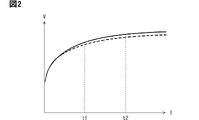
- the capacitance of the smoothing capacitor 440 decreases in this way, charging of the smoothing capacitor 440 can be completed quickly. For example, as shown in FIG. 2, the voltage change becomes faster when the smoothing capacitor 440 is charged.
- the vertical axis indicates voltage and the horizontal axis indicates time.
- Voltage is denoted by V.
- Time is denoted by T.
- a solid line indicates the voltage change of the deteriorated smoothing capacitor 440 .
- a dashed line indicates the voltage change of the undegraded smoothing capacitor 440 .
- the degraded smoothing capacitor 440 and the undegraded smoothing capacitor 440 have different voltages and different voltage changes over time (voltage changes).
- the voltage change of the degraded smoothing capacitor 440 during the transitional period (during charging) from the start to the end of charging is larger than the voltage change of the undegraded smoothing capacitor 440 .
- the capacitance of the smoothing capacitor 440 decreases, voltage smoothing by the smoothing capacitor 440 is impaired.
- the voltage of the fully charged smoothing capacitor 440 during use tends to fluctuate over time.
- the voltage change of the degraded smoothing capacitor 440 is greater than the voltage change of the undegraded smoothing capacitor 440 .
- the vertical axis indicates voltage and the horizontal axis indicates time. Voltage is denoted by V and time is denoted by T. A voltage change of the smoothing capacitor 440 that has deteriorated is indicated by a solid line, and a voltage change of the undegraded smoothing capacitor 440 is indicated by a broken line.
- the smoothing capacitor 440 when power conversion is performed in the power conversion device 400 by controlling switching of a plurality of switches included in the power conversion device 400 between an energized state and a cut-off state. be.
- the smoothing capacitor 440 is used is when the flow direction of the current flowing through the smoothing capacitor 440 changes on the order of microseconds due to power conversion. This is the time when the charge/discharge of the smoothing capacitor 440 changes on the order of microseconds due to power conversion.
- Reactor 420 has a winding core and windings.
- a winding wire is an insulated wire having a conductive wire and an insulating coating covering the conductive wire.
- Reactor 420 is configured by winding this winding around a winding core.
- the inductance of reactor 420 is proportional to the number of turns of this winding.
- a computing unit 408 of the EVECU 406 sequentially acquires the voltage of the smoothing capacitor 440 from the physical quantity sensor 403 in order to detect deterioration of the smoothing capacitor 440 and the reactor 420 .
- the calculation unit 408 calculates the time change (voltage change) of the voltage of the smoothing capacitor 440 .
- the calculation unit 408 sequentially acquires the temperature of the reactor 420 from the physical quantity sensor 403 .
- the calculation unit 408 calculates the time change (temperature change) of the temperature of the reactor 420 .
- the storage unit 407 of the EVECU 406 stores the charging determination value and the smoothing determination value as reference values.
- the charge determination value is determined based on the voltage change of smoothing capacitor 440 when non-degraded smoothing capacitor 440 is charged with power supply power of second battery 220 via non-degraded reactor 420 .
- the smoothing determination value is determined based on the voltage change of undegraded fully charged smoothing capacitor 440 when a plurality of switches included in converter 401 and inverter 402 are controlled to switch.
- At least one of the first temperature determination value and the second temperature determination value is stored in the storage unit 407 as a reference value.
- the first temperature determination value is determined based on the temperature change of undegraded reactor 420 during energization.
- the second temperature determination value is determined based on the durable temperature of reactor 420 .
- EVECU 406 corresponds to a deterioration determination device.
- Arithmetic unit 408 acquires a voltage change of smoothing capacitor 440 when smoothing capacitor 440 is charged. Then, the calculation unit 408 determines whether or not the voltage change is higher (faster) than the charge determination value. If the voltage change is higher than the charge determination value, calculation unit 408 determines that at least one of reactor 420 and smoothing capacitor 440 has deteriorated. When the voltage change is equal to or less than the charge determination value, calculation unit 408 determines that reactor 420 and smoothing capacitor 440 are normal.
- the voltage change is sharper at the start of charging than at the end of charging.
- the voltage change at time t1 is steeper than the voltage change at time t2.
- the voltage change is significantly different depending on time.
- the calculation unit 408 may calculate, for example, a voltage change at a time when charging of the smoothing capacitor 440 is expected to end (expected charging time), and compare the voltage change with the charge determination value. good.
- This expected charging time is determined based on the time required to charge the undegraded smoothing capacitor 440 .
- the expected charging time is stored in the storage unit 407 as a reference value.
- the charging determination value is determined based on the voltage change during this expected charging time.
- the expected charging time may be the time itself required for charging the undegraded smoothing capacitor 440, or may be shorter than that time.
- the expected charging time may be, for example, about 9/10 or 7/8 of that time.
- the calculation unit 408 acquires the voltage change of the fully charged smoothing capacitor 440 while driving the power conversion device 400 . Then, the calculation unit 408 determines whether or not the voltage change is higher (faster) than the smoothed determination value. When the voltage change is higher than the smoothing determination value, the calculation unit 408 determines that the smoothing capacitor 440 has deteriorated. If the voltage change is equal to or less than the smoothing determination value, the calculation unit 408 determines that the smoothing capacitor 440 is normal.
- the calculation unit 408 acquires the temperature change of the reactor 420 in the energized state. The calculation unit 408 determines whether the temperature change is higher (faster) than the first temperature determination value. If the temperature change is higher than the first temperature determination value, calculation unit 408 determines that reactor 420 has deteriorated. When the temperature change is equal to or less than the first temperature determination value, calculation unit 408 determines that reactor 420 is normal.
- the calculation unit 408 may, for example, calculate the temperature change of the reactor 420 when the temperature of the reactor 420 reaches or exceeds a predetermined temperature, and compare the temperature change with the first temperature determination value.
- This predetermined temperature is stored in the storage unit 407 as a reference value.
- calculation unit 408 may determine whether or not the temperature of the reactor 420 is higher than the second temperature determination value. If the temperature is higher than the second temperature determination value, calculation unit 408 determines that reactor 420 has deteriorated. When the temperature is equal to or lower than the second temperature determination value, calculation unit 408 determines that reactor 420 is normal.
- the second temperature determination value is a temperature higher than the predetermined temperature.
- step S10 the calculation unit 408 determines whether or not the smoothing capacitor 440 is in a charged state. If smoothing capacitor 440 is in a charged state, operation unit 408 proceeds to step S20. If smoothing capacitor 440 is not in a charged state, operation unit 408 proceeds to step S30.
- the calculation unit 408 controls charging of the smoothing capacitor 440 .
- the computing unit 408 acquires the charging start time. This charging start time is stored in the storage unit 407 .
- the calculation unit 408 acquires the voltage of the smoothing capacitor 440 from the physical quantity sensor 403. At this time, the calculation unit 408 detects the voltage at different times. Based on these multiple voltages, the calculation unit 408 calculates the voltage change of the smoothing capacitor 440 . After that, the calculation unit 408 proceeds to step S40.
- the calculation unit 408 may measure time from the charging start time of the smoothing capacitor 440 . Then, in step S20, the calculation unit 408 may calculate a voltage change after the charging expected time has elapsed from the charging start time.
- the calculation unit 408 determines whether or not the voltage change is greater than the charge determination value stored in the storage unit 407. If the voltage change is greater than the charge determination value, the calculation unit 408 proceeds to step S50. If the voltage change is equal to or less than the charging determination value, the calculation unit 408 proceeds to step S60.
- the calculation unit 408 determines that at least one of the reactor 420 and the smoothing capacitor 440 has deteriorated. The calculation unit 408 then stores the deterioration determination in the storage unit 407 . At the same time, the calculation unit 408 outputs the deterioration determination to the notification device of the electric vehicle. This notifies the user of the electric vehicle of the deterioration determination. After notification of the deterioration determination, the calculation unit 408 ends the deterioration determination process.
- the calculation unit 408 determines that the reactor 420 and the smoothing capacitor 440 are normal. Then, the calculation unit 408 stores the normality determination in the storage unit 407 . At the same time, the calculation unit 408 outputs the normality determination to the notification device. Thereby, the normal determination is notified to the user. After notification of the normality determination, the computing unit 408 terminates the deterioration determination process.
- step S10 when it is determined in step S10 that the smoothing capacitor 440 is not in a charged state and the process proceeds to step S30, the calculation unit 408 determines whether the power conversion device 400 is performing power conversion. That is, the calculation unit 408 determines whether or not the switch included in the power conversion device 400 is controlled to switch. When switching is controlled, the calculation unit 408 proceeds to step S70. If switching control is not performed, the calculation unit 408 terminates the deterioration determination process.
- the calculation unit 408 acquires the voltage of the smoothing capacitor 440 and the temperature of the reactor 420 from the physical quantity sensor 403. At this time, the calculation unit 408 detects voltage and temperature at different times. Based on this, the calculation unit 408 calculates voltage change and temperature change. After that, the calculation unit 408 proceeds to step S80.
- the temperature change may be calculated when the temperature of the reactor 420 reaches or exceeds a predetermined temperature. Moreover, when the deterioration determination of the reactor 420 is performed based on the temperature of the reactor 420, it is not necessary to calculate the temperature change.
- the calculation unit 408 determines whether or not the voltage change is greater than the smoothed determination value stored in the storage unit 407. If the voltage change is greater than the smoothing determination value, the calculation unit 408 proceeds to step S90. If the voltage change is equal to or less than the smoothing determination value, the calculation unit 408 proceeds to step S100.
- the calculation unit 408 determines that the smoothing capacitor 440 has deteriorated. Then, the calculation unit 408 stores the deterioration determination of the smoothing capacitor 440 in the storage unit 407 . At the same time, the calculation unit 408 outputs the deterioration determination of the smoothing capacitor 440 to the notification device. Thereby, the deterioration determination of the smoothing capacitor 440 is notified to the user. After this, the calculation unit 408 proceeds to step S110.
- the calculation unit 408 determines that the smoothing capacitor 440 is normal. Then, the calculation unit 408 stores the normality determination of the smoothing capacitor 440 in the storage unit 407 . At the same time, the calculation unit 408 outputs the normality determination of the smoothing capacitor 440 to the notification device. Thereby, the user is notified of the normality determination of the smoothing capacitor 440 . After this, the calculation unit 408 proceeds to step S110.
- the calculation unit 408 determines whether or not the temperature change or the temperature is greater than the first temperature determination value or the second temperature determination value stored in the storage unit 407 .
- the calculation unit 408 determines whether the temperature change is greater than the first temperature determination value.
- the calculation unit 408 determines whether the temperature is higher than the second temperature determination value.
- the temperature change and the temperature are collectively referred to as the temperature state, and the first temperature determination value and the second temperature determination value are collectively referred to as the temperature determination value. It is determined whether it is greater (higher) than If the temperature state is greater than the temperature judgment value, the calculation unit 408 proceeds to step S120. When the temperature state is equal to or lower than the temperature judgment value, the calculation unit 408 proceeds to step S130.
- the calculation unit 408 determines that the reactor 420 has deteriorated. Then, calculation unit 408 stores the deterioration determination of reactor 420 in storage unit 407 . At the same time, the calculation unit 408 outputs the deterioration determination of the reactor 420 to the notification device. Thereby, the deterioration determination of the reactor 420 is notified to the user. After the deterioration notification of the reactor 420, the calculation unit 408 ends the deterioration determination process.
- the calculation unit 408 determines that the reactor 420 is normal. Then, calculation unit 408 stores the normality determination of reactor 420 in storage unit 407 . At the same time, the calculation unit 408 outputs the normality determination of the reactor 420 to the notification device. This notifies the user of the normality determination of reactor 420 . After the reactor 420 is notified of normality, the calculation unit 408 terminates the deterioration determination process.
- the execution order of the state determination processing of the smoothing capacitor 440 in steps S80 to S100 and the state determination processing of the reactor 420 in steps S110 to S130 is not particularly limited. The execution order of these two types of state determination processing may be reversed from the execution order shown in FIG.
- the smoothing capacitor 440 is charged when the power conversion device 400 is not in use. After charging the smoothing capacitor 440, the power conversion device 400 is used. Therefore, after the processing of steps S20 and steps S40 to S60 shown in FIG. 4, the processing of steps S30 and steps S70 to S130 is executed. That is, after the combined deterioration determination of reactor 420 and smoothing capacitor 440, deterioration determination of reactor 420 and smoothing capacitor 440 is performed individually.
- step S50 when the deterioration determination in step S50 is performed, it is expected that at least one of step S90 and step S120 is performed. If the determination of normality in step S60 is performed, it is expected that steps S100 and S130 will each be performed.
- the computing unit 408 determines that the reliability of the deterioration determination and the normality determination is low. If the reliability of the determination is low, the calculation unit 408 may output a determination error display to the leaving device. This notifies the user of the determination error.
- the deterioration determination of reactor 420 may be performed when power conversion is not performed in power converter 400 .
- Deterioration determination of reactor 420 can be performed when current is flowing through reactor 420 .
- the deterioration determination of the reactor 420 may be performed after step S50 or step S60.
- the deterioration determination of reactor 420 may be performed while first SMR 310 and second SMR 320 are controlled to be energized in order to adjust the SOC of first battery 210 and second battery 220 .
- the calculation unit 408 may determine the drive limit of the power conversion device 400 .
- the drive limitation is, for example, the limitation of the amount of current applied to the power conversion device 400 and the applied voltage. Further, the calculation unit 408 may decide to strengthen the cooling of the power conversion device 400 by the cooler.
- calculation unit 408 determines that at least one of reactor 420 and smoothing capacitor 440 has deteriorated. Conversely, if the change in voltage of smoothing capacitor 440 during charging is equal to or less than the charge determination value, arithmetic unit 408 determines that reactor 420 and smoothing capacitor 440 are normal.
- the calculation unit 408 determines that the reactor 420 has deteriorated.
- the calculation unit 408 determines that the smoothing capacitor 440 has deteriorated.
- the deterioration of each of the reactor 420 and the smoothing capacitor 440 can be determined individually. Therefore, for example, if the reactor 420 and the smoothing capacitor 440 are individually replaceable modules from the power conversion device 400, only the faulty module can be replaced among these two modules.
- the deterioration determination of the reactor 420 and the smoothing capacitor 440 is performed based on the voltage change and the charge determination value when the smoothing capacitor 440 is charged.
- deterioration determination of the reactor 420 and the smoothing capacitor 440 is performed based on the charging time of the smoothing capacitor 440 .
- the computing unit 408 executes the deterioration determination process shown in FIG. While smoothing capacitor 440 is being charged, operation unit 408 executes steps S210 to S230 instead of step S40.
- the computing unit 408 acquires the voltage of the charged smoothing capacitor 440 at different times in step S20. Then, the calculation unit 408 calculates the voltage change. After that, the calculation unit 408 proceeds to step S210.
- the calculation unit 408 determines whether or not the voltage change has become smaller than a predetermined value. If the voltage change is not smaller than the predetermined value, the calculation unit 408 repeatedly executes steps S20 and S210. The calculation unit 408 enters a standby state. When the voltage change becomes smaller than the predetermined value because smoothing capacitor 440 is nearing a fully charged state, operation unit 408 proceeds to step S220.
- the predetermined value described above is a value larger than the voltage detection error.
- the predetermined value is a value for determining whether the smoothing capacitor 440 is fully charged.
- the predetermined value is stored in storage unit 407 as a reference value.
- the calculation unit 408 calculates the charging time of the smoothing capacitor 440 based on the time when the voltage change becomes smaller than a predetermined value and the charging start time of the smoothing capacitor 440. After that, the calculation unit 408 proceeds to step S230.
- the calculation unit 408 determines whether the charging time is shorter than the expected charging time. If the charging time is shorter than the expected charging time, the calculation unit 408 proceeds to step S50. If the charging time is equal to or longer than the expected charging time, the calculation unit 408 proceeds to step S60.
- the power conversion device 400 described in this embodiment includes components equivalent to the power conversion device 400 described in the first embodiment. Therefore, it goes without saying that the power conversion device 400 of the present embodiment has the same effect as the power conversion device 400 described in the first embodiment. Therefore, description thereof is omitted.
Landscapes
- Engineering & Computer Science (AREA)
- Power Engineering (AREA)
- Physics & Mathematics (AREA)
- General Physics & Mathematics (AREA)
- Inverter Devices (AREA)
- Testing Electric Properties And Detecting Electric Faults (AREA)
- Dc-Dc Converters (AREA)
Abstract
EVECUは電力変換装置に含まれるリアクトルと平滑コンデンサの劣化判定を行う。EVECUは記憶部と演算部を有する。記憶部は、未劣化のリアクトルを介して供給される電源電力による未劣化の平滑コンデンサの充電時の電圧変化に基づく充電判定値を記憶している。演算部は、リアクトルを介して供給される電源電力による平滑コンデンサの充電時の電圧変化が充電判定値よりも大きい場合、リアクトルおよび平滑コンデンサのうちの少なくとも一方が劣化していると判定する。
Description
この出願は、2021年4月2日に日本に出願された特許出願第2021-063599号を基礎としており、基礎の出願の内容を、全体的に、参照により援用している。
本明細書に記載の開示は、劣化判定装置、および、電力変換装置に関するものである。
特許文献1に示されるように、コンデンサ劣化診断装置が知られている。コンデンサ劣化診断装置は、インバータ装置に含まれるアルミ電解コンデンサの周囲空気の湿度に基づいて、アルミ電解コンデンサの劣化判定を行っている。
特許文献1に示される技術内容は、アルミ電解コンデンサの劣化判定に特化している。そのため、特許文献1に示される技術内容では、電力変換を行う装置に含まれる他の受動素子の劣化判定を行いがたくなっている。
本開示の目的は、異種類の受動素子の劣化判定を行うことのできる劣化判定装置、および、電力変換装置を提供することである。
本開示の一態様による劣化判定装置は、電力変換装置に含まれるリアクトルと平滑コンデンサの劣化判定を行う劣化判定装置であって、
未劣化のリアクトルを介して供給される電源電力による未劣化の平滑コンデンサの充電時の電圧変化に基づく充電判定値を記憶する記憶部と、
リアクトルを介して供給される電源電力による平滑コンデンサの充電時の電圧変化が充電判定値よりも大きい場合、リアクトルおよび平滑コンデンサのうちの少なくとも一方が劣化していると判定する演算部と、を有する。
未劣化のリアクトルを介して供給される電源電力による未劣化の平滑コンデンサの充電時の電圧変化に基づく充電判定値を記憶する記憶部と、
リアクトルを介して供給される電源電力による平滑コンデンサの充電時の電圧変化が充電判定値よりも大きい場合、リアクトルおよび平滑コンデンサのうちの少なくとも一方が劣化していると判定する演算部と、を有する。
本開示の一態様による劣化判定装置は、電力変換装置に含まれるリアクトルと平滑コンデンサの劣化判定を行う劣化判定装置であって、
未劣化のリアクトルを介して供給される電源電力による未劣化の平滑コンデンサの充電が完了することの期待される充電期待時間を記憶する記憶部と、
リアクトルを介して供給される電源電力による平滑コンデンサの充電が開始してから終了するまでの充電時間が充電期待時間よりも短い場合、リアクトルおよび平滑コンデンサのうちの少なくとも一方が劣化していると判定する演算部と、を有する。
未劣化のリアクトルを介して供給される電源電力による未劣化の平滑コンデンサの充電が完了することの期待される充電期待時間を記憶する記憶部と、
リアクトルを介して供給される電源電力による平滑コンデンサの充電が開始してから終了するまでの充電時間が充電期待時間よりも短い場合、リアクトルおよび平滑コンデンサのうちの少なくとも一方が劣化していると判定する演算部と、を有する。
本開示の一態様による電力変換装置は、電源電力の供給されるリアクトルと、
リアクトルを介して供給される電源電力によって充電される平滑コンデンサと、
未劣化のリアクトルを介して供給される電源電力による未劣化の平滑コンデンサの充電時の電圧変化に基づく充電判定値を記憶する記憶部と、
平滑コンデンサの充電時の電圧変化が充電判定値よりも高い場合、リアクトルおよび平滑コンデンサのうちの少なくとも一方が劣化していると判定する演算部と、を有する。
リアクトルを介して供給される電源電力によって充電される平滑コンデンサと、
未劣化のリアクトルを介して供給される電源電力による未劣化の平滑コンデンサの充電時の電圧変化に基づく充電判定値を記憶する記憶部と、
平滑コンデンサの充電時の電圧変化が充電判定値よりも高い場合、リアクトルおよび平滑コンデンサのうちの少なくとも一方が劣化していると判定する演算部と、を有する。
これによればリアクトルと平滑コンデンサの劣化判定を行うことができる。異種類の受動素子の劣化判定を行うことができる。
なお、上記の括弧内の参照番号は、後述の実施形態に記載の構成との対応関係を示すものに過ぎず、技術的範囲を何ら制限するものではない。
以下、図面を参照しながら本開示を実施するための複数の形態を説明する。各形態において先行する形態で説明した事項に対応する部分には同一の参照符号を付して重複する説明を省略する場合がある。各形態において構成の一部のみを説明している場合は、構成の他の部分については先行して説明した他の形態を適用することができる。
各実施形態で具体的に組み合わせが可能であることを明示している部分同士の組み合わせが可能である。また、特に組み合わせに支障が生じなければ、組み合わせが可能であることを明示していなくても、実施形態同士、実施形態と変形例、および、変形例同士を部分的に組み合せることも可能である。
(第1実施形態)
<車載システム>
先ず、図1に基づいて車載システム100を説明する。この車載システム100は電気自動車などの電動車両のシステムを構成している。車載システム100は、バッテリ200、システムスイッチ300、電力変換装置400、および、モータ500を有する。
<車載システム>
先ず、図1に基づいて車載システム100を説明する。この車載システム100は電気自動車などの電動車両のシステムを構成している。車載システム100は、バッテリ200、システムスイッチ300、電力変換装置400、および、モータ500を有する。
車載システム100には、上記構成要素に含まれる各種電気部品を電気的に接続するための構成要素として、Pバスバ610、Mバスバ620、および、Nバスバ630が含まれている。また車載システム100には、Uバスバ641、Vバスバ642、および、Wバスバ643が含まれている。
バッテリ200、システムスイッチ300、および、電力変換装置400それぞれに含まれる各種電気部品は、Pバスバ610、Mバスバ620、および、Nバスバ630を介して電気的に接続されている。電力変換装置400に含まれる各種電気部品とモータ500は、Uバスバ641、Vバスバ642、および、Wバスバ643を介して電気的に接続されている。
また、車載システム100は複数のECUを有する。これら複数のECUはバス配線を介して相互に電気信号を送受信している。複数のECUは協調して電動車両を制御している。複数のECUの制御により、バッテリ200のSOCに応じたモータ500の力行と回生が制御される。SOCはstate of chargeの略である。ECUはelectronic control unitの略である。
<バッテリ>
バッテリ200は第1バッテリ210と第2バッテリ220を有する。第1バッテリ210と第2バッテリ220それぞれは複数の電池スタックを有する。複数の電池スタックは電気的に直列接続若しくは並列接続されている。なお、第1バッテリ210と第2バッテリ220のうちの少なくとも一方が1つの電池スタックを有する構成を採用することもできる。
バッテリ200は第1バッテリ210と第2バッテリ220を有する。第1バッテリ210と第2バッテリ220それぞれは複数の電池スタックを有する。複数の電池スタックは電気的に直列接続若しくは並列接続されている。なお、第1バッテリ210と第2バッテリ220のうちの少なくとも一方が1つの電池スタックを有する構成を採用することもできる。
電池スタックは電気的に直列接続された複数の二次電池を有する。二次電池としてはリチウムイオン二次電池、ニッケル水素二次電池、および、有機ラジカル電池などを採用することができる。
第1バッテリ210の正極にPバスバ610が接続されている。第2バッテリ220の正極にMバスバ620が接続されている。第1バッテリ210と第2バッテリ220それぞれの負極にNバスバ630が接続されている。
第1バッテリ210の負極と第2バッテリ220の負極とがNバスバ630を介して常時電気的に接続されている。そのために第1バッテリ210と第2バッテリ220それぞれの負極側の電位が同一になっている。
<システムスイッチ>
システムスイッチ300はバッテリ200と電力変換装置400との間の電力の通電と遮断を制御する。システムスイッチ300は、第1SMR310、第2SMR320、および、第3SMR330を有する。SMRはsystem main relayの略である。
システムスイッチ300はバッテリ200と電力変換装置400との間の電力の通電と遮断を制御する。システムスイッチ300は、第1SMR310、第2SMR320、および、第3SMR330を有する。SMRはsystem main relayの略である。
第1SMR310、第2SMR320、および、第3SMR330それぞれは機械式スイッチである。機械式スイッチは、制御信号の非入力の時に通電状態になる、ノーマリクローズ式スイッチである。
第1SMR310はPバスバ610に設けられる。第2SMR320はMバスバ620に設けられる。第3SMR330はNバスバ630に設けられる。
第1SMR310と第3SMR330は、第1バッテリ210と電力変換装置400との間の通電と遮断とを制御する。第2SMR320と第3SMR330は、第2バッテリ220と電力変換装置400との間の通電と遮断とを制御する。そして、第1SMR310と第2SMR320は、第1バッテリ210の正極と第2バッテリ220の正極との間の通電と遮断とを制御する。
システムスイッチ300は上記構成要素の他に、プリチャージ回路340を有する。プリチャージ回路340は充電スイッチ341と充電抵抗342を有する。これら充電スイッチ341と充電抵抗342が直列接続されて、直列回路が構成されている。
本実施形態では、プリチャージ回路340は第3SMR330に並列接続される。プリチャージ回路340は第3SMR330の迂回経路を構成している。
充電スイッチ341は第3SMR330が通電状態のときに遮断状態に制御される。充電スイッチ341は第3SMR330が遮断状態のときに通電状態に制御される。充電スイッチ341は後述の平滑コンデンサ440を充電する際に通電状態に制御される。
<電力変換装置>
電力変換装置400はバッテリ200とモータ500との間の電力変換を行う。電力変換装置400はコンバータ401、インバータ402、物理量センサ403、および、制御基板404を備えている。
電力変換装置400はバッテリ200とモータ500との間の電力変換を行う。電力変換装置400はコンバータ401、インバータ402、物理量センサ403、および、制御基板404を備えている。
コンバータ401はバッテリ200の直流電力をモータ500の力行に適した電圧レベルに昇圧する。インバータ402はこの直流電力を交流電力に変換する。この交流電力がモータ500に供給される。
インバータ402はモータ500の発電(回生)によって生成された交流電力を直流電力に変換する。コンバータ401はこの直流電力をバッテリ200の充電に適した電圧レベルに降圧する。この降圧された直流電力がバッテリ200と各種電気負荷に供給される。
物理量センサ403は、コンバータ401とインバータ402の物理量を検出する。物理量センサ403が検出する物理量としては、例えば、温度、電流、電圧などがある。物理量センサ403は、コンバータ401とインバータ402に含まれる各種電気部品や、上記した各種バスバに設けられる。
制御基板404は、コンバータ401とインバータ402に含まれるスイッチを通電状態と遮断状態とに制御する機能を果たす。本実施形態の制御基板404は、システムスイッチ300に含まれるスイッチを通電状態と遮断状態とに制御する機能も果たす。
制御基板404にはゲートドライバ405が含まれている。本実施形態では、この制御基板404に複数のECUのうちの1つのEVECU406が含まれている。図面では、ゲートドライバ405をGDと表記している。
なお、ゲートドライバ405とEVECU406とが別々の基板に含まれる構成を採用することもできる。係る構成の場合、ゲートドライバ405を含む基板とEVECU406を含む基板とは、例えばワイヤハーネスを介して電気的に接続される。
制御基板404には、物理量センサ403で検出された物理量が入力される。また制御基板404には、他のECUから車両状態が入力される。EVECU406は入力される各種情報に基づいて、スイッチを制御するための制御信号を生成する。この制御信号が、ゲートドライバ405に入力される。図面では、EVECU406と他のECUとの間の電気信号の送受信を白抜き矢印で示している。
ゲートドライバ405は入力された制御信号を増幅する。この増幅された制御信号が、システムスイッチ300、コンバータ401、および、インバータ402に含まれるスイッチに入力される。これによりスイッチが通電状態と遮断状態とに制御される。
<モータ>
モータ500は図示しない電動車両の出力軸に連結されている。モータ500の回転エネルギーは出力軸を介して電動車両の走行輪に伝達される。逆に、走行輪の回転エネルギーは出力軸を介してモータ500に伝達される。
モータ500は図示しない電動車両の出力軸に連結されている。モータ500の回転エネルギーは出力軸を介して電動車両の走行輪に伝達される。逆に、走行輪の回転エネルギーは出力軸を介してモータ500に伝達される。
モータ500は電力変換装置400から供給される交流電力によって力行する。これにより推進力が走行輪に与えられる。またモータ500は走行輪から伝達される回転エネルギーによって回生する。この回生によって発生した交流電力は、電力変換装置400によって直流電力に変換されるとともに降圧される。この直流電力がバッテリ200に供給される。また直流電力は電動車両に搭載された各種電気負荷にも供給される。
なお、バッテリ200が燃料電池を備える構成を採用することもできる。この場合、回生によって発生した交流電力は、バッテリ200の充電に活用されなくなる。
<電力変換装置の詳細構成>
次に、電力変換装置400の詳細構成を説明する。上記したように電力変換装置400はコンバータ401とインバータ402を備えている。
次に、電力変換装置400の詳細構成を説明する。上記したように電力変換装置400はコンバータ401とインバータ402を備えている。
コンバータ401はPバスバ610とNバスバ630を介して第1バッテリ210と電気的に接続されている。それとともにコンバータ401はMバスバ620とNバスバ630を介して第2バッテリ220と電気的に接続されている。コンバータ401とバッテリ200との間の電気的な接続はシステムスイッチ300によって制御される。
インバータ402はPバスバ610とNバスバ630を介してコンバータ401と電気的に接続されている。それとともにインバータ402はUバスバ641、Vバスバ642、および、Wバスバ643を介してモータ500のステータコイルと電気的に接続されている。インバータ402とバッテリ200との間の電気的な接続はシステムスイッチ300によって制御される。なお、厳密に言えば、インバータ402と第2バッテリ220との間の電気的な接続状態はコンバータ401によっても制御される。
<コンバータ>
コンバータ401はフィルタコンデンサ410、リアクトル420、および、A相スイッチモジュール430を有する。フィルタコンデンサ410の有する2つの電極のうちの一方がMバスバ620に接続されている。フィルタコンデンサ410の有する2つの電極のうちの他方がNバスバ630に接続されている。リアクトル420はMバスバ620に設けられている。A相スイッチモジュール430はPバスバ610、Mバスバ620、および、Nバスバ630それぞれに接続されている。
コンバータ401はフィルタコンデンサ410、リアクトル420、および、A相スイッチモジュール430を有する。フィルタコンデンサ410の有する2つの電極のうちの一方がMバスバ620に接続されている。フィルタコンデンサ410の有する2つの電極のうちの他方がNバスバ630に接続されている。リアクトル420はMバスバ620に設けられている。A相スイッチモジュール430はPバスバ610、Mバスバ620、および、Nバスバ630それぞれに接続されている。
A相スイッチモジュール430は第1スイッチ431と第2スイッチ432を有する。またA相スイッチモジュール430は第1ダイオード433と第2ダイオード434を有する。これら半導体素子が封止樹脂によって被覆されている。
本実施形態では、第1スイッチ431と第2スイッチ432としてnチャネル型のIGBTを採用している。図1に示すように第1スイッチ431のエミッタ電極と第2スイッチ432のコレクタ電極とが接続されている。これにより第1スイッチ431と第2スイッチ432が電気的に直列接続されている。
また、第1スイッチ431のコレクタ電極に第1ダイオード433のカソード電極が接続されている。第1スイッチ431のエミッタ電極に第1ダイオード433のアノード電極が接続されている。これにより第1スイッチ431に第1ダイオード433が逆並列接続されている。
同様にして、第2スイッチ432のコレクタ電極に第2ダイオード434のカソード電極が接続されている。第2スイッチ432のエミッタ電極に第2ダイオード434のアノード電極が接続されている。これにより第2スイッチ432に第2ダイオード434が逆並列接続されている。
第1スイッチ431と第2スイッチ432それぞれのコレクタ電極、エミッタ電極、および、ゲート電極それぞれに端子が接続されている。これら複数の端子の先端が封止樹脂の外に露出されている。これら複数の端子の先端がPバスバ610、Mバスバ620、Nバスバ630、および、制御基板404に選択的に接続されている。
第1スイッチ431のコレクタ電極がPバスバ610に接続されている。第1スイッチ431のエミッタ電極と第2スイッチ432のコレクタ電極とがMバスバ620に接続されている。第2スイッチ432のエミッタ電極がNバスバ630に接続されている。
これにより第1スイッチ431と第2スイッチ432はPバスバ610からNバスバ630へ向かって順に直列接続されている。第1スイッチ431と第2スイッチ432との間の中点に、Mバスバ620に設けられたリアクトル420が接続されている。
Pバスバ610における第1バッテリ210との接続点と第1スイッチ431との接続点との間に第1SMR310が設けられている。Mバスバ620における第2バッテリ220との接続点とリアクトル420との間に第2SMR320が設けられている。Nバスバ630における第1バッテリ210との接続点と第2スイッチ432との接続点との間に第3SMR330が設けられている。また、Nバスバ630における第2バッテリ220との接続点と第2スイッチ432との接続点との間に第3SMR330が設けられている。
そのため、第2SMR320の遮断状態において、第1SMR310と第3SMR330が通電状態になると、直列接続された第1スイッチ431と第2スイッチ432の両端に第1バッテリ210の電源電圧が印加される。第1SMR310の遮断状態において、第2SMR320と第3SMR330が通電状態になると、第2スイッチ432の両端に第2バッテリ220の電源電圧が印加される。
第1スイッチ431と第2スイッチ432それぞれのゲート電極は制御基板404に接続されている。このゲート電極に制御信号が入力される。これにより、第1スイッチ431と第2スイッチ432それぞれが通電状態と遮断状態とに制御される。
なお、コンバータ401に含まれる半導体素子の構成材料としては、Siなどの半導体、および、SiCなどのワイドギャップ半導体を採用することができる。半導体素子の構成材料は特に限定されない。
そして、この半導体素子に含まれる第1スイッチ431と第2スイッチ432としては、IGBTではなくMOSFETを採用することもできる。採用するスイッチ素子の種類は特に限定されない。
<インバータ>
インバータ402は平滑コンデンサ440と放電抵抗450を有する。またインバータ402はU相スイッチモジュール461、V相スイッチモジュール462、および、W相スイッチモジュール463を有する。これら各種構成要素はPバスバ610とNバスバ630との間で電気的に並列接続されている。
インバータ402は平滑コンデンサ440と放電抵抗450を有する。またインバータ402はU相スイッチモジュール461、V相スイッチモジュール462、および、W相スイッチモジュール463を有する。これら各種構成要素はPバスバ610とNバスバ630との間で電気的に並列接続されている。
平滑コンデンサ440はフィルタコンデンサ410よりも静電容量が多くなっている。電力変換装置400の使用時において、平滑コンデンサ440は満充電状態にされる。電力変換装置400の非使用時において、平滑コンデンサ440は放電状態にされる。
平滑コンデンサ440の有する2つの電極のうちの一方がPバスバ610に接続されている。平滑コンデンサ440の有する2つの電極のうちの他方がNバスバ630に接続されている。
放電抵抗450は、電力変換装置400の非使用時に、平滑コンデンサ440に蓄電された電荷を熱エネルギーに変換する機能を果たす。放電抵抗450の一端がPバスバ610に接続されている。放電抵抗450の他端がNバスバ630に接続されている。
平滑コンデンサ440と放電抵抗450とがPバスバ610とNバスバ630を介して接続されている。平滑コンデンサ440と放電抵抗450とを含む閉ループが構成されている。電力変換装置400の非使用時に、平滑コンデンサ440に蓄電された電荷がこの閉ループを流動する。この閉ループを流れる電荷が放電抵抗450で熱エネルギーに変換される。
U相スイッチモジュール461~W相スイッチモジュール463それぞれは第3スイッチ471と第4スイッチ472を有する。また、U相スイッチモジュール461~W相スイッチモジュール463それぞれは第3ダイオード473と第4ダイオード474を有する。これら半導体素子が封止樹脂によって被覆されている。
本実施形態では、第3スイッチ471と第4スイッチ472としてnチャネル型のIGBTを採用している。図1に示すように第3スイッチ471のエミッタ電極と第4スイッチ472のコレクタ電極とが接続されている。これにより第3スイッチ471と第4スイッチ472が電気的に直列接続されている。
第3スイッチ471のコレクタ電極に第3ダイオード473のカソード電極が接続されている。第3スイッチ471のエミッタ電極に第3ダイオード473のアノード電極が接続されている。これにより第3スイッチ471に第3ダイオード473が逆並列接続されている。
同様にして、第4スイッチ472のコレクタ電極に第4ダイオード474のカソード電極が接続されている。第4スイッチ472のエミッタ電極に第4ダイオード474のアノード電極が接続されている。これにより第4スイッチ472に第4ダイオード474が逆並列接続されている。
これら第3スイッチ471と第4スイッチ472それぞれのコレクタ電極、エミッタ電極、および、ゲート電極それぞれに端子が接続されている。これら複数の端子の先端が封止樹脂の外に露出されている。これら複数の端子の先端がPバスバ610、Nバスバ630、Uバスバ641、Vバスバ642、Wバスバ643、および、制御基板404に選択的に接続されている。
第3スイッチ471のコレクタ電極がPバスバ610に接続されている。第4スイッチ472のエミッタ電極がNバスバ630に接続されている。これにより第3スイッチ471と第4スイッチ472はPバスバ610からNバスバ630へ向かって順に直列接続されている。
以上に示した接続構成のため、第2SMR320の遮断状態において、第1SMR310と第3SMR330が通電状態になると、直列接続された第3スイッチ471と第4スイッチ472の両端に第1バッテリ210の電源電圧が印加される。第1SMR310の遮断状態において、第2SMR320と第3SMR330が通電状態になると、コンバータ401が昇降圧動作をしていない場合、直列接続された第3スイッチ471と第4スイッチ472の両端に第2バッテリ220の電源電圧が印加される。
また、U相スイッチモジュール461の備える第3スイッチ471と第4スイッチ472との間の中点がUバスバ641を介してモータ500のU相ステータコイルに接続されている。V相スイッチモジュール462の備える第3スイッチ471と第4スイッチ472との間の中点がVバスバ642を介してモータ500のV相ステータコイルに接続されている。W相スイッチモジュール463の備える第3スイッチ471と第4スイッチ472との間の中点がWバスバ643を介してモータ500のW相ステータコイルに接続されている。これにより、U相スイッチモジュール461~W相スイッチモジュール463がモータ500のU相ステータコイル~W相ステータコイルに個別に接続されている。
第3スイッチ471と第4スイッチ472それぞれのゲート電極が制御基板404に接続されている。これにより、第3スイッチ471と第4スイッチ472それぞれの通電状態と遮断状態とが制御基板404によって制御可能になっている。
なお、これら第3スイッチ471と第4スイッチ472としては、コンバータ401と同様にしてIGBTではなくMOSFETを採用することもできる。インバータ402に含まれる半導体素子の構成材料としては、コンバータ401と同様にして、Siなどの半導体、および、SiCなどのワイドギャップ半導体などを採用することができる。インバータ402に含まれる半導体素子の構成材料と、コンバータ401に含まれる半導体素子の構成材料とは、同一でも不同でもよい。
<物理量センサ>
上記したように物理量センサ403は、コンバータ401とインバータ402の物理量を検出する。具体的には、物理量センサ403は、平滑コンデンサ440の電圧とリアクトル420の温度を検出する。
上記したように物理量センサ403は、コンバータ401とインバータ402の物理量を検出する。具体的には、物理量センサ403は、平滑コンデンサ440の電圧とリアクトル420の温度を検出する。
物理量センサ403は、平滑コンデンサ440やPバスバ610に設けられた電圧センサを有する。この電圧センサによって平滑コンデンサ440の電圧が検出される。
物理量センサ403は、リアクトル420や電力変換装置400のスイッチに設けられた温度センサを有する。この温度センサによってリアクトル420の温度が検出される。
なお、物理量センサ403は、Pバスバ610とMバスバ620を流れる直流電流を検出する電流センサを有してもよい。物理量センサ403は、Uバスバ641、Vバスバ642、および、Wバスバ643を流れる交流電流を検出する電流センサを有してもよい。
<制御基板>
上記したように、制御基板404にはゲートドライバ405とEVECU406が含まれている。EVECU406は図1に示す記憶部407と演算部408を有する。
上記したように、制御基板404にはゲートドライバ405とEVECU406が含まれている。EVECU406は図1に示す記憶部407と演算部408を有する。
記憶部407はコンピュータやプロセッサによって読み取り可能なデータとプログラムを非一時的に記憶する非遷移的実体的記憶媒体である。記憶部407は揮発性メモリと不揮発性メモリとを有している。記憶部407は制御基板404に入力された諸情報や演算部408の処理結果を記憶する。記憶部407は演算部408が演算処理するための各種プログラムと各種参照値を記憶している。
演算部408にはプロセッサが含まれている。演算部408は制御基板404に入力された諸情報を記憶部407に記憶する。演算部408は記憶部407に記憶された情報に基づいて各種演算処理を実行する。
演算部408は制御信号を生成する。この制御信号がゲートドライバ405で増幅される。この制御信号によって、システムスイッチ300、コンバータ401、および、インバータ402に含まれるスイッチが通電状態と遮断状態とに制御される。
<スイッチ制御>
平滑コンデンサ440を充電する場合、EVECU406は第1SMR310を遮断状態、第2SMR320を通電状態にする。それとともに、EVECU406は第3SMR330を遮断状態、充電スイッチ341を通電状態にする。そして、EVECU406はコンバータ401とインバータ402に含まれるスイッチを遮断状態にする。
平滑コンデンサ440を充電する場合、EVECU406は第1SMR310を遮断状態、第2SMR320を通電状態にする。それとともに、EVECU406は第3SMR330を遮断状態、充電スイッチ341を通電状態にする。そして、EVECU406はコンバータ401とインバータ402に含まれるスイッチを遮断状態にする。
これにより、平滑コンデンサ440がリアクトル420を介して第2バッテリ220から供給される電源電力によって充電される。なお、第2バッテリ220の正極と平滑コンデンサ440との間の通電経路には、リアクトル420の他に、第1スイッチ431と第1ダイオード433がある。EVECU406はこの第1スイッチ431を通電状態にしてもよい。
例えば第2バッテリ220のSOCが著しく低下した場合、EVECU406は第1SMR310を通電状態、第2SMR320を遮断状態にしてもよい。これにより、第1バッテリ210から供給される電源電力によって平滑コンデンサ440が充電される。
平滑コンデンサ440の充電が終了した後、EVECU406は第3SMR330を遮断状態から通電状態に切り換える。またEVECU406は充電スイッチ341を通電状態から遮断状態に切り換える。これにより充電抵抗342での電力消費がなくなる。第2バッテリ220の電源電力が各種電気負荷に供給される。
モータ500を駆動する場合、EVECU406は第1SMR310を遮断状態、第2SMR320を通電状態にする。それとともに、EVECU406は第3SMR330を通電状態、充電スイッチ341を遮断状態にする。そして、EVECU406はコンバータ401とインバータ402に含まれるスイッチを通電状態と遮断状態とに制御する。なお、EVECU406は第1SMR310を通電状態、第2SMR320を遮断状態にしてもよい。
EVECU406はコンバータ401とインバータ402に含まれるスイッチの制御信号としてパルス信号を生成している。EVECU406はこのパルス信号のオンデューティ比と周波数を調整している。このオンデューティ比と周波数は物理量センサ403で検出される物理量、および、他のECUから入力される車両情報に基づいて決定される。この車両情報には、モータ500の回転角、モータ500の目標トルク、および、バッテリ200のSOCなどが含まれている。
第2バッテリ220から供給される直流の電源電力を昇圧する場合、EVECU406はA相スイッチモジュール430の第1スイッチ431を遮断状態に固定する。それとともにEVECU406はA相スイッチモジュール430の第2スイッチ432を通電状態と遮断状態とに順次切り換える。
供給される直流電力を降圧する場合、EVECU406はA相スイッチモジュール430の第2スイッチ432を遮断状態に固定する。それとともにEVECU406はA相スイッチモジュール430の第1スイッチ431を通電状態と遮断状態とに順次切り換える。
モータ500を力行する場合、EVECU406はU相スイッチモジュール461~W相スイッチモジュール463の備える第3スイッチ471と第4スイッチ472それぞれをPWM制御する。これによりインバータ402で3相交流が生成される。
モータ500が発電(回生)する場合、EVECU406は例えばU相スイッチモジュール461~W相スイッチモジュール463の備える第3スイッチ471と第4スイッチ472それぞれへの制御信号の出力を停止する。これによりモータ500の発電によって生成された交流電力がU相スイッチモジュール461~W相スイッチモジュール463の備えるダイオードを通る。この結果、交流電力が直流電力に変換される。
モータ500の駆動制御を終えて、平滑コンデンサ440を放電する場合、EVECU406は、システムスイッチ300、コンバータ401、および、インバータ402それぞれに含まれるスイッチを遮断状態にする。この結果、平滑コンデンサ440に蓄電された電荷が放電抵抗450を流れる。この電荷が放電抵抗450で積極的に熱エネルギーに変換される。
なお、第1バッテリ210と第2バッテリ220のSOCを調整する場合、EVECU406は第1SMR310と第2SMR320を通電状態にする。それとともに、EVECU406は第3SMR330と充電スイッチ341を遮断状態にする。EVECU406は第1スイッチ431を通電状態にする。そしてEVECU406はその他のコンバータ401とインバータ402に含まれるスイッチを遮断状態にする。
これにより、第1バッテリ210と第2バッテリ220を含む閉ループが構成される。第1バッテリ210と第2バッテリ220のうち、出力電圧の高いほうから低いほうへと、第1スイッチ431とリアクトル420を介して電源電力が供給される。第1バッテリ210と第2バッテリ220のうちの一方のSOCが減る代わりに、他方のSOCが増大する。
<要望>
近年、電動車両の自動運転化により、走行距離が増加傾向にある。そして、電動車両に搭載されるモータ500の高出力化に伴い、バッテリ200の電源電力の電圧レベルが増大傾向にある。係る状況下で使用される電力変換装置400に故障が発生することを未然に防ぐために、電力変換装置400に含まれる電気部品の劣化を検出することが望まれている。
近年、電動車両の自動運転化により、走行距離が増加傾向にある。そして、電動車両に搭載されるモータ500の高出力化に伴い、バッテリ200の電源電力の電圧レベルが増大傾向にある。係る状況下で使用される電力変換装置400に故障が発生することを未然に防ぐために、電力変換装置400に含まれる電気部品の劣化を検出することが望まれている。
<平滑コンデンサの劣化>
平滑コンデンサ440は、誘電体を含む絶縁性の樹脂部材と、樹脂部材の一面に設けられた正極と、その裏面に設けられた負極と、を有する。例えば、高電流の通電による発熱などによって、この樹脂部材の一部が劣化すると、その劣化場所で電荷が蓄えられがたくなる。この結果、平滑コンデンサ440の静電容量が減少する。
平滑コンデンサ440は、誘電体を含む絶縁性の樹脂部材と、樹脂部材の一面に設けられた正極と、その裏面に設けられた負極と、を有する。例えば、高電流の通電による発熱などによって、この樹脂部材の一部が劣化すると、その劣化場所で電荷が蓄えられがたくなる。この結果、平滑コンデンサ440の静電容量が減少する。
このように平滑コンデンサ440の静電容量が減少すると、平滑コンデンサ440の充電が早く完了しやすくなる。例えば図2に示すように、平滑コンデンサ440の充電時の電圧変化が速くなる。
図2の縦軸は電圧、横軸は時間を示している。電圧をVで表記している。時間をTで表記している。劣化した平滑コンデンサ440の電圧変化を実線で示している。未劣化の平滑コンデンサ440の電圧変化を破線で示している。
図2に示す時間t1、時間t2それぞれにおいて、劣化した平滑コンデンサ440と未劣化の平滑コンデンサ440とでは、電圧が異なるとともに、電圧の時間変化(電圧変化)が異なっている。充電を開始してから終了するまでの過渡期(充電時)における劣化した平滑コンデンサ440の電圧変化が、未劣化の平滑コンデンサ440の電圧変化よりも大きくなっている。
また、平滑コンデンサ440の静電容量が減少すると、平滑コンデンサ440による電圧の平滑化が損なわれる。例えば図3に示すように、満充電状態の平滑コンデンサ440の使用時の電圧が時間変動しやすくなる。使用時における、劣化した平滑コンデンサ440の電圧変化が、未劣化の平滑コンデンサ440の電圧変化よりも大きくなる。
図3の縦軸は電圧、横軸は時間を示している。電圧をVで表記し、時間をTで表記している。劣化した平滑コンデンサ440の電圧変化を実線、未劣化の平滑コンデンサ440の電圧変化を破線で示している。
なお、平滑コンデンサ440の使用時とは、電力変換装置400に含まれる複数のスイッチが通電状態と遮断状態とに切り換え制御されることで、電力変換装置400で電力変換が行われている時である。平滑コンデンサ440の使用時とは、電力変換のために、平滑コンデンサ440を流れる電流の流動方向がマイクロセカンドオーダーで変化する時である。電力変換のために、平滑コンデンサ440の充放電がマイクロセカンドオーダーで変化する時である。
<リアクトルの劣化>
リアクトル420は、巻き芯と、巻き線と、を有する。巻き線は、導電線と、この導電線を被覆する絶縁被膜と、を有する絶縁電線である。この巻き線が巻き芯に巻きまわされることで、リアクトル420が構成されている。リアクトル420のインダクタンスは、この巻き線の巻き数に比例する。
リアクトル420は、巻き芯と、巻き線と、を有する。巻き線は、導電線と、この導電線を被覆する絶縁被膜と、を有する絶縁電線である。この巻き線が巻き芯に巻きまわされることで、リアクトル420が構成されている。リアクトル420のインダクタンスは、この巻き線の巻き数に比例する。
係る構成のため、例えば、巻き線の絶縁被膜の絶縁性が部分的に損なわれると、巻き回された巻き線が部分的にショートする虞がある。係るショートが起こると、巻き線の巻き数が実質的に減少する。この結果、リアクトル420のインダクタンスが減少する。
このようにリアクトル420のインダクタンスが減少すると、リアクトル420を電流が流れやすくなる。そのため、リアクトル420を介した第2バッテリ220の電源電力による平滑コンデンサ440の充電が早く完了しやすくなる。図2に示すように、平滑コンデンサ440の充電時の電圧変化が速くなる。また、部分的なショートのため、リアクトル420は通電によって昇温しやすくなる。
<劣化判定>
EVECU406の演算部408は、これら平滑コンデンサ440とリアクトル420の劣化を検出するために、物理量センサ403から平滑コンデンサ440の電圧を順次取得している。演算部408は平滑コンデンサ440の電圧の時間変化(電圧変化)を算出している。
EVECU406の演算部408は、これら平滑コンデンサ440とリアクトル420の劣化を検出するために、物理量センサ403から平滑コンデンサ440の電圧を順次取得している。演算部408は平滑コンデンサ440の電圧の時間変化(電圧変化)を算出している。
また、演算部408は物理量センサ403からリアクトル420の温度を順次取得している。演算部408はリアクトル420の温度の時間変化(温度変化)を算出している。
EVECU406の記憶部407には、参照値として、充電判定値と平滑判定値が記憶されている。充電判定値は、未劣化のリアクトル420を介した第2バッテリ220の電源電力によって、未劣化の平滑コンデンサ440が充電されるときの、平滑コンデンサ440の電圧変化に基づいて決定される。平滑判定値は、コンバータ401とインバータ402に含まれる複数のスイッチが切り換え制御されている際における、未劣化の満充電状態の平滑コンデンサ440の電圧変化に基づいて決定される。
また、記憶部407には、参照値として、第1温度判定値と第2温度判定値のうちの少なくとも一方が記憶されている。第1温度判定値は未劣化のリアクトル420の通電時の温度変化に基づいて決定される。第2温度判定値はリアクトル420の耐久温度に基づいて決定される。EVECU406が劣化判定装置に相当する。
<平滑コンデンサの電圧>
演算部408は、平滑コンデンサ440の充電時に平滑コンデンサ440の電圧変化を取得する。そして演算部408はその電圧変化が充電判定値よりも高い(速い)か否かを判定する。電圧変化が充電判定値よりも高い場合、演算部408はリアクトル420と平滑コンデンサ440のうちの少なくとも一方が劣化していると判定する。電圧変化が充電判定値以下の場合、演算部408はリアクトル420と平滑コンデンサ440が正常であると判定する。
演算部408は、平滑コンデンサ440の充電時に平滑コンデンサ440の電圧変化を取得する。そして演算部408はその電圧変化が充電判定値よりも高い(速い)か否かを判定する。電圧変化が充電判定値よりも高い場合、演算部408はリアクトル420と平滑コンデンサ440のうちの少なくとも一方が劣化していると判定する。電圧変化が充電判定値以下の場合、演算部408はリアクトル420と平滑コンデンサ440が正常であると判定する。
図2に示すように、平滑コンデンサ440の劣化状態にかかわらずに、充電の開始時は充電の終了時に比べて電圧変化が急激になっている。時間t1での電圧変化は、時間t2での電圧変化よりも急激になっている。時間によって、電圧変化が著しく異なっている。
そのために演算部408は、例えば、平滑コンデンサ440の充電が終了することの期待される時間(充電期待時間)での電圧変化を算出して、その電圧変化と充電判定値とを比較してもよい。
この充電期待時間は、未劣化の平滑コンデンサ440が充電されるときに要する時間に基づいて決定される。充電期待時間は、参照値として、記憶部407に記憶されている。充電判定値はこの充電期待時間での電圧変化に基づいて決定される。
なお、充電期待時間は、未劣化の平滑コンデンサ440が充電されるときに要する時間そのものでもよいし、その時間よりも短い時間でもよい。充電期待時間は、例えば、その時間の9/10、7/8程度の時間でもよい。
演算部408は、電力変換装置400を駆動している際に、満充電状態の平滑コンデンサ440の電圧変化を取得する。そして演算部408はその電圧変化が平滑判定値よりも高い(速い)か否かを判定する。電圧変化が平滑判定値よりも高い場合、演算部408は平滑コンデンサ440が劣化していると判定する。電圧変化が平滑判定値以下の場合、演算部408は平滑コンデンサ440が正常であると判定する。
<リアクトルの温度>
演算部408は、通電状態のリアクトル420の温度変化を取得する。演算部408はその温度変化が第1温度判定値よりも高い(速い)か否かを判定する。温度変化が第1温度判定値よりも高い場合、演算部408はリアクトル420が劣化していると判定する。温度変化が第1温度判定値以下の場合、演算部408はリアクトル420が正常であると判定する。
演算部408は、通電状態のリアクトル420の温度変化を取得する。演算部408はその温度変化が第1温度判定値よりも高い(速い)か否かを判定する。温度変化が第1温度判定値よりも高い場合、演算部408はリアクトル420が劣化していると判定する。温度変化が第1温度判定値以下の場合、演算部408はリアクトル420が正常であると判定する。
図示しないが、リアクトル420の劣化状態にかかわらずに、未通電状態から通電状態に変わった際、リアクトル420の温度は指数関数的に急増することが想定される。
そのために演算部408は、例えば、リアクトル420の温度が所定温度以上になった場合にリアクトル420の温度変化を算出して、その温度変化と第1温度判定値とを比較してもよい。この所定温度は、参照値として記憶部407に記憶されている。
なお、演算部408はリアクトル420の温度が第2温度判定値よりも高いか否かを判定してもよい。温度が第2温度判定値よりも高い場合、演算部408はリアクトル420が劣化していると判定する。温度が第2温度判定値以下の場合、演算部408はリアクトル420が正常であると判定する。第2温度判定値は上記の所定温度よりも高い温度である。
<劣化判定処理>
次に、図4に基づいて劣化判定処理を説明する。電動車両のイグニッションスイッチがオフ状態からオン状態に切り換わると、演算部408は劣化判定処理を実行する。演算部408は劣化判定処理をサイクルタスクで繰り返し実行している。なお、図面では開始をSで表記している。終了をEで表記している。
次に、図4に基づいて劣化判定処理を説明する。電動車両のイグニッションスイッチがオフ状態からオン状態に切り換わると、演算部408は劣化判定処理を実行する。演算部408は劣化判定処理をサイクルタスクで繰り返し実行している。なお、図面では開始をSで表記している。終了をEで表記している。
ステップS10で演算部408は、平滑コンデンサ440が充電状態か否かを判定する。平滑コンデンサ440が充電状態である場合、演算部408はステップS20へ進む。平滑コンデンサ440が充電状態ではない場合、演算部408はステップS30へ進む。
なお、平滑コンデンサ440の充電を制御するのは演算部408である。係る平滑コンデンサ440の充電を実行している場合、その充電の開始時間を演算部408は取得している。この充電開始時間は記憶部407に記憶される。
ステップS20へ進むと演算部408は、物理量センサ403から平滑コンデンサ440の電圧を取得する。この際、演算部408は異なる時間で電圧を検出する。これら複数の電圧に基づいて、演算部408は平滑コンデンサ440の電圧変化を算出する。この後に演算部408はステップS40へ進む。
なお演算部408は、平滑コンデンサ440の充電開始時間から時間を計測してもよい。そして演算部408は、ステップS20において充電開始時間から充電期待時間経過後の電圧変化を算出してもよい。
ステップS40へ進むと演算部408は、電圧変化が記憶部407に記憶されている充電判定値よりも大きいか否かを判定する。電圧変化が充電判定値よりも大きい場合、演算部408はステップS50へ進む。電圧変化が充電判定値以下の場合、演算部408はステップS60へ進む。
ステップS50へ進むと演算部408は、リアクトル420と平滑コンデンサ440のうちの少なくとも一方が劣化していると判定する。そして演算部408はその劣化判定を記憶部407に記憶する。それとともに演算部408はその劣化判定を電動車両の報知装置に出力する。これにより、劣化判定が電動車両のユーザに通知される。係る劣化判定の通知の後に演算部408は劣化判定処理を終了する。
ステップS60へ進むと演算部408は、リアクトル420と平滑コンデンサ440は正常であると判定する。そして演算部408はその正常判定を記憶部407に記憶する。それとともに演算部408はその正常判定を報知装置に出力する。これにより、正常判定がユーザに通知される。係る正常判定の通知の後に演算部408は劣化判定処理を終了する。
フローを遡って、ステップS10で平滑コンデンサ440が充電状態ではないと判定してステップS30へ進むと演算部408は、電力変換装置400が電力変換を行っているか否かを判定する。すなわち演算部408は、電力変換装置400に含まれるスイッチが切り換え制御されているか否かを判定する。切り換え制御されている場合、演算部408はステップS70へ進む。切り換え制御されていない場合、演算部408は劣化判定処理を終了する。
ステップS70へ進むと演算部408は、物理量センサ403から平滑コンデンサ440の電圧とリアクトル420の温度を取得する。この際、演算部408は異なる時間で電圧と温度を検出する。これに基づいて、演算部408は電圧変化と温度変化を算出する。この後に演算部408はステップS80へ進む。
なお、温度変化の算出は、リアクトル420の温度が所定温度以上になった場合に行ってもよい。また、リアクトル420の劣化判定をリアクトル420の温度に基づいて行う場合、温度変化を算出しなくともよい。
ステップS80へ進むと演算部408は、電圧変化が記憶部407に記憶されている平滑判定値よりも大きいか否かを判定する。電圧変化が平滑判定値よりも大きい場合、演算部408はステップS90へ進む。電圧変化が平滑判定値以下の場合、演算部408はステップS100へ進む。
ステップS90へ進むと演算部408は、平滑コンデンサ440が劣化していると判定する。そして演算部408は平滑コンデンサ440の劣化判定を記憶部407に記憶する。それとともに演算部408は平滑コンデンサ440の劣化判定を報知装置に出力する。これにより、平滑コンデンサ440の劣化判定がユーザに通知される。この後に演算部408はステップS110へ進む。
ステップS100へ進むと演算部408は、平滑コンデンサ440は正常であると判定する。そして演算部408は平滑コンデンサ440の正常判定を記憶部407に記憶する。それとともに演算部408は平滑コンデンサ440の正常判定を報知装置に出力する。これにより、平滑コンデンサ440の正常判定がユーザに通知される。この後に演算部408はステップS110へ進む。
ステップS110へ進むと演算部408は、温度変化若しくは温度が記憶部407に記憶されている第1温度判定値若しくは第2温度判定値よりも大きいか否かを判定する。温度変化に基づいて劣化判定を行う場合、演算部408は、温度変化が第1温度判定値よりも大きいか否かを判定する。温度に基づいて劣化判定を行う場合、演算部408は温度が第2温度判定値よりも大きいか否かを判定する。
温度変化と温度とをまとめて温度状態、第1温度判定値と第2温度判定値とをまとめて温度判定値と表記すると、ステップS110において演算部408は、リアクトル420の温度状態が温度判定値よりも大きい(高い)か否かを判定する。温度状態が温度判定値よりも大きい場合、演算部408はステップS120へ進む。温度状態が温度判定値以下の場合、演算部408はステップS130へ進む。
ステップS120へ進むと演算部408は、リアクトル420が劣化していると判定する。そして演算部408はリアクトル420の劣化判定を記憶部407に記憶する。それとともに演算部408はリアクトル420の劣化判定を報知装置に出力する。これにより、リアクトル420の劣化判定がユーザに通知される。係るリアクトル420の劣化通知の後に演算部408は劣化判定処理を終了する。
ステップS130へ進むと演算部408は、リアクトル420は正常であると判定する。そして演算部408はリアクトル420の正常判定を記憶部407に記憶する。それとともに演算部408はリアクトル420の正常判定を報知装置に出力する。これにより、リアクトル420の正常判定がユーザに通知される。係るリアクトル420の正常通知の後に演算部408は劣化判定処理を終了する。
なお、ステップS80~ステップS100の平滑コンデンサ440の状態判定処理と、ステップS110~ステップS130のリアクトル420の状態判定処理の実行順序は特に限定されない。これら2種類の状態判定処理の実行順序を図4に示す実行順序とは逆にしてもよい。
これまでに説明したように、平滑コンデンサ440の充電は、電力変換装置400の未使用時に行われる。平滑コンデンサ440の充電後に、電力変換装置400が使用される。そのため、図4に示すステップS20、ステップS40~ステップS60の処理の後に、ステップS30、ステップS70~ステップS130の処理が実行される。すなわち、リアクトル420と平滑コンデンサ440を合わせた劣化判定の後に、リアクトル420と平滑コンデンサ440の個別の劣化判定が行われる。
したがって、例えば、ステップS50の劣化判定が実行された場合、ステップS90とステップS120のうちの少なくとも1つが実行されることが期待される。ステップS60の正常判定が実行された場合、ステップS100とステップS130それぞれが実行されることが期待される。
これらの期待が外れた場合、演算部408は劣化判定と正常判定の信頼性が低いと判定する。判定の信頼性が低い場合、演算部408は判定のエラー表示を放置装置に出力してもよい。これにより、判定のエラーがユーザに通知される。
なお、図4に示す劣化判定処理とは異なり、リアクトル420の劣化判定は、電力変換装置400で電力変換が実行されていない時に実行されてもよい。リアクトル420の劣化判定は、リアクトル420に電流が流れている時であれば、実行することができる。
例えば、ステップS50若しくはステップS60の後に、リアクトル420の劣化判定を行ってもよい。第1バッテリ210と第2バッテリ220のSOCを調整するために第1SMR310と第2SMR320が通電状態に制御されている際に、リアクトル420の劣化判定を行ってもよい。
そして、リアクトル420と平滑コンデンサ440のうちの少なくとも一方が劣化していると判定した場合、演算部408は電力変換装置400の駆動制限を決定してもよい。駆動制限とは、例えば、電力変換装置400の通電電流量や印加電圧の制限である。また、演算部408は冷却器による電力変換装置400の冷却を強めることを決定してもよい。
<作用効果>
これまでに説明したように、充電時の平滑コンデンサ440の電圧変化が充電判定値よりも大きい場合、演算部408はリアクトル420と平滑コンデンサ440のうちの少なくとも一方が劣化していると判定する。逆に、充電時の平滑コンデンサ440の電圧変化が充電判定値以下の場合、演算部408はリアクトル420と平滑コンデンサ440が正常であると判定する。
これまでに説明したように、充電時の平滑コンデンサ440の電圧変化が充電判定値よりも大きい場合、演算部408はリアクトル420と平滑コンデンサ440のうちの少なくとも一方が劣化していると判定する。逆に、充電時の平滑コンデンサ440の電圧変化が充電判定値以下の場合、演算部408はリアクトル420と平滑コンデンサ440が正常であると判定する。
このように、充電時の電圧変化を検出するだけで、リアクトル420と平滑コンデンサ440の劣化判定を合わせて行うことができる。異種類の受動素子の劣化判定を行うことができる。
通電状態のリアクトル420の温度状態が温度判定値よりも高い場合、演算部408はリアクトル420が劣化していると判定する。切り換え制御時の満充電状態の平滑コンデンサ440の電圧変化が平滑判定値よりも高い場合、演算部408は平滑コンデンサ440が劣化していると判定する。
このように、リアクトル420と平滑コンデンサ440それぞれの劣化を個別に判定することができる。そのため、例えば、リアクトル420と平滑コンデンサ440それぞれが電力変換装置400から個別に交換可能なモジュールの場合、これら2つのモジュールのうち、故障しているモジュールだけを交換することができる。
(第2実施形態)
次に、第2実施形態を図5に基づいて説明する。
次に、第2実施形態を図5に基づいて説明する。
第1実施形態では、平滑コンデンサ440の充電時に電圧変化と充電判定値とに基づいて、リアクトル420と平滑コンデンサ440の劣化判定を行う例を示した。これに対し本実施形態では、平滑コンデンサ440の充電時間に基づいて、リアクトル420と平滑コンデンサ440の劣化判定を行う。
この場合、演算部408は図5に示す劣化判定処理を実行する。平滑コンデンサ440が充電されている際に、演算部408はステップS40に代わって、ステップS210~ステップS230を実行する。
第1実施形態で説明したように演算部408は、ステップS20において充電状態の平滑コンデンサ440の電圧を異なる時間で取得する。そして演算部408は電圧変化を算出する。この後に演算部408はステップS210へ進む。
ステップS210へ進むと演算部408は、電圧変化が所定値よりも小さくなったか否かを判定する。電圧変化が所定値よりも小さくない場合、演算部408はステップS20とステップS210を繰り返し実行する。演算部408は待機状態になる。平滑コンデンサ440が満充電状態に近づいたために、電圧変化が所定値よりも小さくなった場合、演算部408はステップS220へ進む。
なお、上記した所定値は電圧の検出誤差よりも大きな値である。所定値は平滑コンデンサ440の満充電状態を判定するための値である。所定値は参照値として記憶部407に記憶されている。
ステップS220へ進むと演算部408は、電圧変化が所定値よりも小さくなった際の時間と、平滑コンデンサ440の充電開始時間と、に基づいて平滑コンデンサ440の充電時間を算出する。この後、演算部408はステップS230へ進む。
ステップS230へ進むと演算部408は、充電時間が充電期待時間よりも短いか否かを判定する。充電時間が充電期待時間よりも短い場合、演算部408はステップS50へ進む。充電時間が充電期待時間以上の場合、演算部408はステップS60へ進む。
本実施形態に記載の電力変換装置400には、第1実施形態に記載の電力変換装置400と同等の構成要素が含まれている。そのために本実施形態の電力変換装置400が第1実施形態に記載の電力変換装置400と同等の作用効果を奏することは言うまでもない。そのためにその記載を省略する。
本開示は、実施例に準拠して記述されたが、本開示は当該実施例や構造に限定されるものではないと理解される。本開示は、様々な変形例や均等範囲内の変形をも包含する。加えて、様々な組み合わせや形態が本開示に示されているが、それらに一要素のみ、それ以上、あるいはそれ以下、を含む他の組み合わせや形態をも、本開示の範疇や思想範囲に入るものである。
Claims (6)
- 電力変換装置(400)に含まれるリアクトル(420)と平滑コンデンサ(440)の劣化判定を行う劣化判定装置であって、
未劣化の前記リアクトルを介して供給される電源電力による未劣化の前記平滑コンデンサの充電時の電圧変化に基づく充電判定値を記憶する記憶部(407)と、
前記リアクトルを介して供給される前記電源電力による前記平滑コンデンサの充電時の電圧変化が前記充電判定値よりも大きい場合、前記リアクトルおよび前記平滑コンデンサのうちの少なくとも一方が劣化していると判定する演算部(408)と、を有する劣化判定装置。 - 電力変換装置(400)に含まれるリアクトル(420)と平滑コンデンサ(440)の劣化判定を行う劣化判定装置であって、
未劣化の前記リアクトルを介して供給される電源電力による未劣化の前記平滑コンデンサの充電が完了することの期待される充電期待時間を記憶する記憶部(407)と、
前記リアクトルを介して供給される前記電源電力による前記平滑コンデンサの充電が開始してから終了するまでの充電時間が前記充電期待時間よりも短い場合、前記リアクトルおよび前記平滑コンデンサのうちの少なくとも一方が劣化していると判定する演算部(408)と、を有する劣化判定装置。 - 前記記憶部は、前記リアクトルの温度状態を判定するための温度判定値を記憶しており、
前記演算部は、前記リアクトルの温度が前記温度判定値よりも高い場合、前記リアクトルが劣化していると判定する請求項1または請求項2に記載の劣化判定装置。 - 前記記憶部は、前記電力変換装置に含まれる複数のスイッチ(431,432,471,472)が通電状態と遮断状態とに切り換え制御される際における未劣化の満充電状態の前記平滑コンデンサの電圧変化に基づく平滑判定値を記憶しており、
前記演算部は、前記切り換え制御の際における満充電状態の前記平滑コンデンサの電圧変化が前記平滑判定値よりも大きい場合、前記平滑コンデンサが劣化していると判定する請求項1~3のいずれか1項に記載の劣化判定装置。 - 前記記憶部は、前記リアクトルの温度状態を判定するための温度判定値と、前記電力変換装置に含まれる複数のスイッチ(431,432,471,472)が通電状態と遮断状態とに切り換え制御される際における未劣化の満充電状態の前記平滑コンデンサの電圧変化に基づく平滑判定値と、を記憶しており、
前記演算部は、
前記リアクトルの温度が前記温度判定値よりも高く、なおかつ、前記切り換え制御の際における満充電状態の前記平滑コンデンサの電圧変化が前記平滑判定値よりも低い場合、前記リアクトルおよび前記平滑コンデンサのうち前記リアクトルのみが劣化していると判定し、
前記リアクトルの温度が前記温度判定値よりも低く、なおかつ、前記切り換え制御の際における満充電状態の前記平滑コンデンサの電圧変化が前記平滑判定値よりも高い場合、前記リアクトルおよび前記平滑コンデンサのうち前記平滑コンデンサのみが劣化していると判定する請求項1または請求項2に記載の劣化判定装置。 - 電源電力の供給されるリアクトル(420)と、
前記リアクトルを介して供給される前記電源電力によって充電される平滑コンデンサ(440)と、
未劣化の前記リアクトルを介して供給される前記電源電力による未劣化の前記平滑コンデンサの充電時の電圧変化に基づく充電判定値を記憶する記憶部(407)と、
前記平滑コンデンサの充電時の電圧変化が前記充電判定値よりも高い場合、前記リアクトルおよび前記平滑コンデンサのうちの少なくとも一方が劣化していると判定する演算部(408)と、を有する電力変換装置。
Priority Applications (1)
| Application Number | Priority Date | Filing Date | Title |
|---|---|---|---|
| US18/476,850 US20240019503A1 (en) | 2021-04-02 | 2023-09-28 | Deterioration determination device, and power conversion device |
Applications Claiming Priority (2)
| Application Number | Priority Date | Filing Date | Title |
|---|---|---|---|
| JP2021-063599 | 2021-04-02 | ||
| JP2021063599A JP2022158589A (ja) | 2021-04-02 | 2021-04-02 | 劣化判定装置、および、電力変換装置 |
Related Child Applications (1)
| Application Number | Title | Priority Date | Filing Date |
|---|---|---|---|
| US18/476,850 Continuation US20240019503A1 (en) | 2021-04-02 | 2023-09-28 | Deterioration determination device, and power conversion device |
Publications (1)
| Publication Number | Publication Date |
|---|---|
| WO2022209975A1 true WO2022209975A1 (ja) | 2022-10-06 |
Family
ID=83458787
Family Applications (1)
| Application Number | Title | Priority Date | Filing Date |
|---|---|---|---|
| PCT/JP2022/012375 WO2022209975A1 (ja) | 2021-04-02 | 2022-03-17 | 劣化判定装置、および、電力変換装置 |
Country Status (3)
| Country | Link |
|---|---|
| US (1) | US20240019503A1 (ja) |
| JP (1) | JP2022158589A (ja) |
| WO (1) | WO2022209975A1 (ja) |
Families Citing this family (1)
| Publication number | Priority date | Publication date | Assignee | Title |
|---|---|---|---|---|
| WO2024096055A1 (ja) * | 2022-11-04 | 2024-05-10 | 株式会社Gsユアサ | 電源機器の遠隔診断装置、遠隔診断システム及びコンピュータプログラム |
Citations (7)
| Publication number | Priority date | Publication date | Assignee | Title |
|---|---|---|---|---|
| JPH02266820A (ja) * | 1989-04-04 | 1990-10-31 | Fuji Electric Co Ltd | 電力変換装置用平滑コンデンサの寿命判定回路 |
| JPH05215800A (ja) * | 1992-02-04 | 1993-08-24 | Toyota Autom Loom Works Ltd | コンデンサの劣化診断方法 |
| JP2009189214A (ja) * | 2008-02-08 | 2009-08-20 | Toyota Motor Corp | 駆動装置およびこれが備えるコンデンサの異常判定方法 |
| JP2012115018A (ja) * | 2010-11-24 | 2012-06-14 | Toyota Motor Corp | 電力制御装置 |
| JP2012228965A (ja) * | 2011-04-26 | 2012-11-22 | Toyota Motor Corp | ハイブリッド車両の制御装置 |
| JP2018004523A (ja) * | 2016-07-06 | 2018-01-11 | 東洋電機製造株式会社 | コンデンサ状態判定装置 |
| WO2018216208A1 (ja) * | 2017-05-26 | 2018-11-29 | 三菱電機株式会社 | 電力変換装置 |
-
2021
- 2021-04-02 JP JP2021063599A patent/JP2022158589A/ja active Pending
-
2022
- 2022-03-17 WO PCT/JP2022/012375 patent/WO2022209975A1/ja active Application Filing
-
2023
- 2023-09-28 US US18/476,850 patent/US20240019503A1/en active Pending
Patent Citations (7)
| Publication number | Priority date | Publication date | Assignee | Title |
|---|---|---|---|---|
| JPH02266820A (ja) * | 1989-04-04 | 1990-10-31 | Fuji Electric Co Ltd | 電力変換装置用平滑コンデンサの寿命判定回路 |
| JPH05215800A (ja) * | 1992-02-04 | 1993-08-24 | Toyota Autom Loom Works Ltd | コンデンサの劣化診断方法 |
| JP2009189214A (ja) * | 2008-02-08 | 2009-08-20 | Toyota Motor Corp | 駆動装置およびこれが備えるコンデンサの異常判定方法 |
| JP2012115018A (ja) * | 2010-11-24 | 2012-06-14 | Toyota Motor Corp | 電力制御装置 |
| JP2012228965A (ja) * | 2011-04-26 | 2012-11-22 | Toyota Motor Corp | ハイブリッド車両の制御装置 |
| JP2018004523A (ja) * | 2016-07-06 | 2018-01-11 | 東洋電機製造株式会社 | コンデンサ状態判定装置 |
| WO2018216208A1 (ja) * | 2017-05-26 | 2018-11-29 | 三菱電機株式会社 | 電力変換装置 |
Also Published As
| Publication number | Publication date |
|---|---|
| US20240019503A1 (en) | 2024-01-18 |
| JP2022158589A (ja) | 2022-10-17 |
Similar Documents
| Publication | Publication Date | Title |
|---|---|---|
| US7269535B2 (en) | Fault diagnosing apparatus for vehicle and fault diagnosing method for vehicle | |
| JP4807058B2 (ja) | 車両用電源装置 | |
| US10202042B2 (en) | Electric vehicle power conversion system | |
| US11458844B2 (en) | Power supply system for vehicle | |
| US7813849B2 (en) | Vehicle control system | |
| US20150331472A1 (en) | Dual power supply system and electrically driven vehicle | |
| JP7140045B2 (ja) | 駆動回路 | |
| US9843184B2 (en) | Voltage conversion apparatus | |
| JP4457626B2 (ja) | 組電池の異常判定装置および組電池の異常判定方法 | |
| US11400917B2 (en) | Power supply system for vehicle | |
| US20240019503A1 (en) | Deterioration determination device, and power conversion device | |
| JP6376422B2 (ja) | 充放電装置 | |
| US11110801B2 (en) | Fault diagnosis system of power converter for electric vehicle | |
| US10892635B2 (en) | Redundant power supply | |
| JP5011978B2 (ja) | 蓄電装置 | |
| JP5304279B2 (ja) | 蓄電装置 | |
| US20220393633A1 (en) | Power converter control circuit | |
| JP6617653B2 (ja) | 電源装置 | |
| JP2018165080A (ja) | 車両電源装置 | |
| JP7021661B2 (ja) | 電源装置の制御装置 | |
| JP5076918B2 (ja) | 蓄電装置 | |
| JP7276080B2 (ja) | 異常判定装置 | |
| JP2020048301A (ja) | 電力変換装置 | |
| WO2022019038A1 (ja) | 電力変換器の制御回路 | |
| JP5277819B2 (ja) | 蓄電装置 |
Legal Events
| Date | Code | Title | Description |
|---|---|---|---|
| 121 | Ep: the epo has been informed by wipo that ep was designated in this application |
Ref document number: 22780194 Country of ref document: EP Kind code of ref document: A1 |
|
| NENP | Non-entry into the national phase |
Ref country code: DE |
|
| 122 | Ep: pct application non-entry in european phase |
Ref document number: 22780194 Country of ref document: EP Kind code of ref document: A1 |