WO2022209170A1 - スパッタリングターゲット - Google Patents
スパッタリングターゲット Download PDFInfo
- Publication number
- WO2022209170A1 WO2022209170A1 PCT/JP2022/001705 JP2022001705W WO2022209170A1 WO 2022209170 A1 WO2022209170 A1 WO 2022209170A1 JP 2022001705 W JP2022001705 W JP 2022001705W WO 2022209170 A1 WO2022209170 A1 WO 2022209170A1
- Authority
- WO
- WIPO (PCT)
- Prior art keywords
- gallium nitride
- sputtering
- sputtering target
- crystal
- oxygen concentration
- Prior art date
- Legal status (The legal status is an assumption and is not a legal conclusion. Google has not performed a legal analysis and makes no representation as to the accuracy of the status listed.)
- Ceased
Links
Images
Classifications
-
- C—CHEMISTRY; METALLURGY
- C23—COATING METALLIC MATERIAL; COATING MATERIAL WITH METALLIC MATERIAL; CHEMICAL SURFACE TREATMENT; DIFFUSION TREATMENT OF METALLIC MATERIAL; COATING BY VACUUM EVAPORATION, BY SPUTTERING, BY ION IMPLANTATION OR BY CHEMICAL VAPOUR DEPOSITION, IN GENERAL; INHIBITING CORROSION OF METALLIC MATERIAL OR INCRUSTATION IN GENERAL
- C23C—COATING METALLIC MATERIAL; COATING MATERIAL WITH METALLIC MATERIAL; SURFACE TREATMENT OF METALLIC MATERIAL BY DIFFUSION INTO THE SURFACE, BY CHEMICAL CONVERSION OR SUBSTITUTION; COATING BY VACUUM EVAPORATION, BY SPUTTERING, BY ION IMPLANTATION OR BY CHEMICAL VAPOUR DEPOSITION, IN GENERAL
- C23C14/00—Coating by vacuum evaporation, by sputtering or by ion implantation of the coating forming material
- C23C14/22—Coating by vacuum evaporation, by sputtering or by ion implantation of the coating forming material characterised by the process of coating
- C23C14/34—Sputtering
- C23C14/3407—Cathode assembly for sputtering apparatus, e.g. Target
- C23C14/3414—Metallurgical or chemical aspects of target preparation, e.g. casting, powder metallurgy
-
- C—CHEMISTRY; METALLURGY
- C30—CRYSTAL GROWTH
- C30B—SINGLE-CRYSTAL GROWTH; UNIDIRECTIONAL SOLIDIFICATION OF EUTECTIC MATERIAL OR UNIDIRECTIONAL DEMIXING OF EUTECTOID MATERIAL; REFINING BY ZONE-MELTING OF MATERIAL; PRODUCTION OF A HOMOGENEOUS POLYCRYSTALLINE MATERIAL WITH DEFINED STRUCTURE; SINGLE CRYSTALS OR HOMOGENEOUS POLYCRYSTALLINE MATERIAL WITH DEFINED STRUCTURE; AFTER-TREATMENT OF SINGLE CRYSTALS OR A HOMOGENEOUS POLYCRYSTALLINE MATERIAL WITH DEFINED STRUCTURE; APPARATUS THEREFOR
- C30B29/00—Single crystals or homogeneous polycrystalline material with defined structure characterised by the material or by their shape
- C30B29/10—Inorganic compounds or compositions
- C30B29/40—AIIIBV compounds wherein A is B, Al, Ga, In or Tl and B is N, P, As, Sb or Bi
- C30B29/403—AIII-nitrides
- C30B29/406—Gallium nitride
-
- C—CHEMISTRY; METALLURGY
- C23—COATING METALLIC MATERIAL; COATING MATERIAL WITH METALLIC MATERIAL; CHEMICAL SURFACE TREATMENT; DIFFUSION TREATMENT OF METALLIC MATERIAL; COATING BY VACUUM EVAPORATION, BY SPUTTERING, BY ION IMPLANTATION OR BY CHEMICAL VAPOUR DEPOSITION, IN GENERAL; INHIBITING CORROSION OF METALLIC MATERIAL OR INCRUSTATION IN GENERAL
- C23C—COATING METALLIC MATERIAL; COATING MATERIAL WITH METALLIC MATERIAL; SURFACE TREATMENT OF METALLIC MATERIAL BY DIFFUSION INTO THE SURFACE, BY CHEMICAL CONVERSION OR SUBSTITUTION; COATING BY VACUUM EVAPORATION, BY SPUTTERING, BY ION IMPLANTATION OR BY CHEMICAL VAPOUR DEPOSITION, IN GENERAL
- C23C14/00—Coating by vacuum evaporation, by sputtering or by ion implantation of the coating forming material
- C23C14/06—Coating by vacuum evaporation, by sputtering or by ion implantation of the coating forming material characterised by the coating material
- C23C14/0617—AIII BV compounds, where A is Al, Ga, In or Tl and B is N, P, As, Sb or Bi
-
- C—CHEMISTRY; METALLURGY
- C23—COATING METALLIC MATERIAL; COATING MATERIAL WITH METALLIC MATERIAL; CHEMICAL SURFACE TREATMENT; DIFFUSION TREATMENT OF METALLIC MATERIAL; COATING BY VACUUM EVAPORATION, BY SPUTTERING, BY ION IMPLANTATION OR BY CHEMICAL VAPOUR DEPOSITION, IN GENERAL; INHIBITING CORROSION OF METALLIC MATERIAL OR INCRUSTATION IN GENERAL
- C23C—COATING METALLIC MATERIAL; COATING MATERIAL WITH METALLIC MATERIAL; SURFACE TREATMENT OF METALLIC MATERIAL BY DIFFUSION INTO THE SURFACE, BY CHEMICAL CONVERSION OR SUBSTITUTION; COATING BY VACUUM EVAPORATION, BY SPUTTERING, BY ION IMPLANTATION OR BY CHEMICAL VAPOUR DEPOSITION, IN GENERAL
- C23C14/00—Coating by vacuum evaporation, by sputtering or by ion implantation of the coating forming material
- C23C14/06—Coating by vacuum evaporation, by sputtering or by ion implantation of the coating forming material characterised by the coating material
- C23C14/0641—Nitrides
-
- C—CHEMISTRY; METALLURGY
- C30—CRYSTAL GROWTH
- C30B—SINGLE-CRYSTAL GROWTH; UNIDIRECTIONAL SOLIDIFICATION OF EUTECTIC MATERIAL OR UNIDIRECTIONAL DEMIXING OF EUTECTOID MATERIAL; REFINING BY ZONE-MELTING OF MATERIAL; PRODUCTION OF A HOMOGENEOUS POLYCRYSTALLINE MATERIAL WITH DEFINED STRUCTURE; SINGLE CRYSTALS OR HOMOGENEOUS POLYCRYSTALLINE MATERIAL WITH DEFINED STRUCTURE; AFTER-TREATMENT OF SINGLE CRYSTALS OR A HOMOGENEOUS POLYCRYSTALLINE MATERIAL WITH DEFINED STRUCTURE; APPARATUS THEREFOR
- C30B28/00—Production of homogeneous polycrystalline material with defined structure
- C30B28/04—Production of homogeneous polycrystalline material with defined structure from liquids
-
- C—CHEMISTRY; METALLURGY
- C30—CRYSTAL GROWTH
- C30B—SINGLE-CRYSTAL GROWTH; UNIDIRECTIONAL SOLIDIFICATION OF EUTECTIC MATERIAL OR UNIDIRECTIONAL DEMIXING OF EUTECTOID MATERIAL; REFINING BY ZONE-MELTING OF MATERIAL; PRODUCTION OF A HOMOGENEOUS POLYCRYSTALLINE MATERIAL WITH DEFINED STRUCTURE; SINGLE CRYSTALS OR HOMOGENEOUS POLYCRYSTALLINE MATERIAL WITH DEFINED STRUCTURE; AFTER-TREATMENT OF SINGLE CRYSTALS OR A HOMOGENEOUS POLYCRYSTALLINE MATERIAL WITH DEFINED STRUCTURE; APPARATUS THEREFOR
- C30B29/00—Single crystals or homogeneous polycrystalline material with defined structure characterised by the material or by their shape
- C30B29/10—Inorganic compounds or compositions
- C30B29/38—Nitrides
-
- H—ELECTRICITY
- H01—ELECTRIC ELEMENTS
- H01J—ELECTRIC DISCHARGE TUBES OR DISCHARGE LAMPS
- H01J37/00—Discharge tubes with provision for introducing objects or material to be exposed to the discharge, e.g. for the purpose of examination or processing thereof
- H01J37/32—Gas-filled discharge tubes
- H01J37/34—Gas-filled discharge tubes operating with cathodic sputtering
- H01J37/3411—Constructional aspects of the reactor
- H01J37/3414—Targets
- H01J37/3426—Material
- H01J37/3429—Plural materials
Definitions
- the present invention relates to a sputtering target made of gallium nitride-based crystals.
- Sputtering is an example of a method for forming a gallium nitride thin film.
- the use of a sputtering target made of, for example, gallium nitride as a raw material is under study.
- a sputtering target there are a target produced by sintering gallium nitride powder (for example, Patent Document 1) and a polycrystalline target produced by a hydride vapor phase deposition method (for example, Patent Document 2, Non-Patent Document 1). Proposed.
- a sputtering target is composed of a polycrystalline body formed by a hydride vapor phase deposition method or a flux method, it is easy to obtain a target with high density.
- a gallium nitride polycrystal for example, as described in Patent Document 2, a different material substrate having a crystal structure and lattice constant significantly different from those of gallium nitride is used as a base substrate, or a low-temperature buffer layer is used.
- a method of forming a film without using is conceivable. In this case, it is easy to take in impurities such as oxygen, and it is difficult to obtain the low oxygen concentration required for the sputtering target.
- Non-Patent Document 1 reports the synthesis of polycrystalline gallium nitride with relatively low oxygen concentration and high density using the CVPR method, which is a vapor phase epitaxy method using a chloride raw material (NH 4 Cl). ing.
- the CVPR method is a vapor phase epitaxy method using a chloride raw material (NH 4 Cl).
- NH 4 Cl chloride raw material
- the inventor also considered using a gallium nitride single crystal substrate as a sputtering target.
- the single crystal substrate is susceptible to cracking during sputtering, and the deposition rate during sputtering is very slow.
- An object of the present invention is to provide a gallium nitride-based gallium sputtering target that has a low oxygen concentration and is less likely to crack during sputtering.
- the present invention provides a sputtering target comprising a gallium nitride-based crystal composed of a plurality of gallium nitride-based single crystal grains oriented in the c-axis direction in the normal direction to a predetermined plane,
- the gallium nitride-based crystal has a total oxygen concentration of 150 mass ppm or less, and the gallium nitride-based single crystal particles have an oxygen concentration measured by a dynamic SIMS method of 2 ⁇ 10 17 cm ⁇ 3 or more.
- This invention relates to a sputtering target.
- the present inventor employed a polycrystalline gallium nitride-based crystal composed of a plurality of gallium nitride-based single crystal grains oriented in the c-axis direction as a sputtering target.
- the quality tends to be uniform, erosion during sputtering (a phenomenon in which the target evaporates unevenly) is suppressed, and the target life is lengthened.
- further lowering the total oxygen concentration of the gallium nitride-based crystal body makes it possible to lower and stabilize the oxygen concentration of the gallium nitride-based crystal film obtained by sputtering.
- the inventors have attempted to further reduce the oxygen concentration in the gallium nitride-based crystal.
- the oxygen concentration of the gallium nitride-based crystal film obtained by sputtering can be lowered, and the quality can be stabilized.
- the measured value of the oxygen concentration of the gallium nitride-based single crystal particles constituting the gallium nitride-based crystal by the dynamic SIMS method at 2 ⁇ 10 17 cm ⁇ 3 or more, cracking of the sputtering target during sputtering is suppressed. We have found that it can be suppressed, and arrived at the present invention.
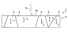
- FIG. 1 is a schematic diagram showing a sputtering target 1.
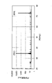
- FIG. An X-ray diffraction chart obtained in an example is shown.
- the sputtering target 1 of the present invention is composed of a plurality of gallium nitride-based single crystal grains 3 oriented in the c-axis direction in a substantially normal direction N to a predetermined surface 2a. It consists of a crystal body 2. That is, the gallium nitride-based crystal body 2 is a polycrystalline body composed of a plurality of gallium nitride-based single crystal particles 3 . Then, the predetermined surface 2a of the gallium nitride-based crystal is used for sputtering. When viewed from the normal direction N to the predetermined surface, the crystal orientation L of each gallium nitride-based single crystal particle 3 is approximately the c-axis orientation.
- the half width of the (002) plane reflection of the X-ray rocking curve of the gallium nitride-based crystal is 1000 seconds or less.
- the quality of the obtained gallium nitride-based crystal is further improved. From this point of view, it is more preferable that the half width of the (002) plane reflection of the X-ray rocking curve of the gallium nitride-based crystal is 800 seconds or less.
- the gallium nitride-based crystal body 2 is an aggregate of single crystal grains having a columnar structure in which a single crystal is observed when viewed in the normal direction N, and grain boundaries are observed when viewed in the horizontal direction. It is also possible to assume that there is Here, the term “columnar structure” does not mean only a typical vertically long columnar shape, but includes various shapes such as a horizontally long shape, a trapezoidal shape, and a shape like an inverted trapezoid. defined as meaning. However, as described above, the gallium nitride-based crystal may have a structure having crystal orientations aligned to some extent in a normal line or similar direction, and does not necessarily have to be a columnar structure in a strict sense.
- the total oxygen concentration of the gallium nitride-based crystal constituting the sputtering target of the present invention is 150 mass ppm or less, and the oxygen concentration of the gallium nitride-based single crystal particles measured by the dynamic SIMS method is 2 ⁇ 10 17 cm ⁇ 3 or more. is.
- the total oxygen concentration of the gallium nitride-based crystal can be measured by elemental analysis, specifically by an oxygen/nitrogen simultaneous analyzer (for example, EMGA-650W (manufactured by HORIBA)).
- the total oxygen concentration of the gallium nitride-based crystal is 150 ppm by mass or less, and more preferably 50 ppm by mass or less.
- the present inventor actually examined it, if the oxygen concentration of the gallium nitride-based crystal becomes too low, the sputtering target tends to crack during sputtering. From the viewpoint of suppressing cracking of the target during sputtering, it was found that a small amount of oxygen should be contained.
- the oxygen concentration of the gallium nitride-based single crystal particles measured by the dynamic SIMS method is preferably 3 ⁇ 10 19 /cm 3 or less, more preferably 1 ⁇ 10 19 /cm 3 or less. It is particularly preferable to set it to ⁇ 10 18 /cm 3 or less.
- the measurement of the oxygen concentration of the gallium nitride-based single crystal particles by the dynamic SIMS method is performed as follows. That is, the oxygen concentration is measured in a square field of 200 ⁇ m ⁇ 200 ⁇ m by dynamic SIMS on a predetermined surface of the gallium nitride-based crystal. This measurement is performed for 9 fields of view, and the average value is calculated.
- Gallium nitride-based crystals are represented by Al x Ga 1-x N and In x Ga 1-x N.
- x is preferably 0.5 or less, and 0.2 or less. is more preferred.
- x may be 0.
- the relative density of the sputtering target measured by the Archimedes method is 98.0% or more, preferably 99.0% or more, and more preferably 99.5% or more.
- Such a high-density gallium nitride-based crystal makes it difficult for erosion and oxidation to occur during sputtering.
- the thickness of the sputtering target is 1 mm or more. More preferably, the thickness is 2 mm or more, more preferably 4 mm or more. Moreover, it is preferable that it is 8 mm or less practically.
- the diameter of the sputtering target is 50 mm or more. This diameter is preferably 75 mm or more, more preferably 100 mm or more. In practice, it is preferably 160 mm or less.
- the sputtering target does not have translucency. That is, the sputtering target is colored. This coloration is considered to be caused by light absorption due to defects such as nitrogen deficiency. Having such defects improves the deposition rate during sputtering.
- the gallium nitride-based single crystal particles have a carbon concentration measured by a dynamic SIMS method of 1 ⁇ 10 16 cm ⁇ 3 or less. This further improves the quality of gallium nitride-based crystals produced by sputtering.
- the germanium concentration of the gallium nitride-based single crystal particles measured by the dynamic SIMS method is 1 ⁇ 10 18 cm ⁇ 3 or more. This makes it possible to obtain a conductive sputtering target in which the resistivity of the target material is lowered. From this point of view, it is more preferable that the germanium concentration of the gallium nitride-based single crystal particles measured by the dynamic SIMS method is 5 ⁇ 10 18 cm ⁇ 3 or more.
- the arithmetic mean roughness Ra of the predetermined surface of the gallium nitride-based crystal is preferably 0.1 ⁇ m or less.
- Gallium nitride-based crystals constituting the sputtering target may be doped with n-type dopants and/or p-type dopants.
- dopants include zinc, calcium, iron, beryllium, magnesium, strontium, cadmium, scandium, Examples include silicon, germanium, and tin.
- a DC sputtering method, an RF sputtering method, an AC sputtering method, a DC magnetron sputtering method, an RF magnetron sputtering method, an ion beam sputtering method, or the like can be appropriately selected.
- the gas pressure during sputtering is preferably 0.05-7.0 Pa.
- the gas for sputtering is preferably a mixed gas of argon (Ar) gas and nitrogen (N 2 ) gas.
- the temperature during sputtering is preferably 100 to 1000.degree.
- Example 1 (Preparation of sputtering target)
- This crucible was placed in a stainless steel inner container, further placed in a stainless steel pressure-resistant container capable of containing it, and closed with a container lid equipped with a nitrogen introduction pipe.
- This pressure vessel was vacuum-baked in advance, placed on a turntable installed in the heating section of the crystal manufacturing apparatus, and the pressure vessel was sealed with a lid.
- the inside of the pressure vessel was evacuated to 0.1 Pa or less with a vacuum pump.
- the upper heater, the middle heater and the lower heater to heat the heating space to 880°C
- This state was maintained for 200 hours to grow a gallium nitride crystal.
- the oxygen source in each container is eliminated as much as possible, the growth temperature of the gallium nitride crystal is lowered to, for example, 800° C. or less, and the direction of rotation of the pressure-resistant container is periodically changed. , the total oxygen concentration of the gallium nitride crystal and the oxygen concentration of the gallium nitride single crystal particles measured by dynamic SIMS were adjusted.
- the prepared sputtering target was cut into 20 mm squares, and the oxygen concentration was measured with an oxygen/nitrogen simultaneous analyzer (EMGA-650W (manufactured by HORIBA)) to obtain 150 mass ppm. Further, the oxygen concentration was measured at 9 points in a region of 200 ⁇ m ⁇ 200 ⁇ m by dynamic SIMS on a predetermined surface of the manufactured sputtering target, and the average value was found to be 2.0 ⁇ 10 17 /cm 3 .
- EMGA-650W oxygen/nitrogen simultaneous analyzer
- the difference between the total oxygen concentration measured by oxygen/nitrogen simultaneous analysis and the oxygen concentration measured by dynamic SIMS is due to the fact that crystal growth was performed at a lower temperature than usual, which improved the growth rate of the facet plane with a large amount of oxygen uptake. It is thought that this reflects the fact that the difference in oxygen concentration between the c-plane growth portion and the facet plane growth portion was generated.
- the carbon concentration measured by dynamic SIMS was 5 ⁇ 10 15 /cm 3 or less at any of the nine measurement points.
- germanium concentration measured by dynamic SIMS was 2 ⁇ 10 16 /cm 3 or less at any of the nine measurement points.
- FIG. 2 is a graph showing the 2 ⁇ - ⁇ measurement results.
- a bonded body was obtained by bonding a sputtering target to a heated copper plate (backing plate) using metal indium.
- an RF sputtering apparatus was used with a chamber atmosphere of Ar 20 sccm, N 2 100 sccm, a chamber pressure of 0.25 Pa, a 2-inch sapphire substrate used as a substrate, a target-substrate distance of 150 mm, and a substrate temperature of was set to 500° C., and a film of gallium nitride crystal was formed by sputtering. Furthermore, the appearance of the sputtering target after sputtering was inspected.
- Example 1 As a result, when the sapphire substrate was taken out after the sputtering process, a uniform gallium nitride crystal film having a thickness of 1 ⁇ m was formed. SIMS analysis of the gallium nitride crystal film revealed that the oxygen concentration was 1 ⁇ 10 17 /cm 3 or less. In addition, no abnormality such as cracks or cracks appeared in the appearance of the sputtering target after sputtering after film formation. The measurement results in Example 1 are summarized in Table 1.
- This crucible was placed in a stainless steel inner container, further placed in a stainless steel pressure-resistant container capable of containing it, and closed with a container lid equipped with a nitrogen introduction pipe.
- This pressure vessel was vacuum-baked in advance, placed on a turntable installed in the heating section of the crystal manufacturing apparatus, and the pressure vessel was sealed with a lid.
- the inside of the pressure vessel was evacuated to 0.1 Pa or less by a vacuum pump.
- the upper heater, the middle heater and the lower heater to heat the heating space to 880°C, introduce nitrogen gas from the nitrogen gas cylinder up to 4.0 MPa, and rotate the outer container around the central axis at 20 rpm. was rotated in constant cycles clockwise and counterclockwise.
- Comparative example 2 When a GaN crystal was grown under the same conditions as in Comparative Example 1 with a holding time of 60 hours, a gallium nitride crystal ingot free from cracks separated from the seed crystal substrate was produced. A predetermined surface of this gallium nitride crystal ingot was polished to obtain a sputtering target having a thickness of 0.8 mm.
- the prepared sputtering target was cut into 20 mm squares, the surface was polished, and the total oxygen concentration was measured with an oxygen/nitrogen simultaneous analyzer (EMGA-650W (manufactured by HORIBA)). ) was below. Further, when the oxygen concentration of the prepared sputtering target was measured at 9 points by dynamic SIMS, all of them were 3 ⁇ 10 16 cm ⁇ 3 or less.
- EMGA-650W manufactured by HORIBA
- the concentration of each element was measured in the same manner as in Example 1, the X-ray diffraction measurement was performed, and the sputtering experiment was performed. Table 1 shows the results. As a result, when the sapphire substrate was taken out after the sputtering process, a uniform gallium nitride crystal film having a thickness of 1 ⁇ m was formed. SIMS analysis of the gallium nitride crystal film revealed that the oxygen concentration was 2 ⁇ 10 17 /cm 3 or more. In addition, no abnormalities such as cracks or cracks appeared in the appearance of the target after sputtering after film formation.
- the concentration of each element was measured in the same manner as in Example 1, the X-ray diffraction measurement was performed, and the sputtering experiment was performed. Table 1 shows the results. Moreover, when sputtering was carried out in the same manner as in Example 1, cracks occurred in the target during sputtering, and the sputtering film formation was stopped.
- a gallium nitride sintered body was produced based on the description in [0067] of WO2016-158651A1 and used as a sputtering target. That is, 200 g of gallium nitride powder having an average particle size of 1 ⁇ m was sintered in a graphite mold of ⁇ 120 mm with a hot press at 1100° C. for 3 hours under a surface pressure of 200 kgf/cm 2 . The sintered body thus obtained was polished to obtain a sputtering target having a thickness of 2.0 mm.
- the total oxygen concentration of the sputtering target of this example was 800 mass ppm. Moreover, the X-ray diffraction result showed a non-oriented state. Also, a sputtering experiment was conducted in the same manner as in Example 1. As a result, when the sapphire substrate was taken out after the sputtering process, a uniform gallium nitride crystal film having a thickness of 1 ⁇ m was formed. SIMS analysis of the gallium nitride crystal film revealed an oxygen concentration of 2 ⁇ 10 20 /cm 3 . In addition, no abnormalities such as cracks or cracks appeared in the appearance of the target after sputtering after film formation.
Landscapes
- Chemical & Material Sciences (AREA)
- Engineering & Computer Science (AREA)
- Organic Chemistry (AREA)
- Materials Engineering (AREA)
- Metallurgy (AREA)
- Chemical Kinetics & Catalysis (AREA)
- Mechanical Engineering (AREA)
- Crystallography & Structural Chemistry (AREA)
- Inorganic Chemistry (AREA)
- Plasma & Fusion (AREA)
- Analytical Chemistry (AREA)
- Physics & Mathematics (AREA)
- Physical Vapour Deposition (AREA)
- Crystals, And After-Treatments Of Crystals (AREA)
Abstract
Description
前記窒化ガリウム系結晶体の全酸素濃度が150質量ppm以下であり、前記窒化ガリウム系単結晶粒子の酸素濃度のダイナミックSIMS法による測定値が2×1017cm-3以上であることを特徴とする、スパッタリングターゲットに係るものである。
図1に模式的に示すように、本発明のスパッタリングターゲット1は、所定面2aに対する略法線方向Nでc軸方位に配向した複数の窒化ガリウム系単結晶粒子3によって構成される窒化ガリウム系結晶体2からなる。
すなわち、窒化ガリウム系結晶体2は、複数の窒化ガリウム系単結晶粒子3によって構成される多結晶体である。そして、窒化ガリウム系結晶体の所定面2aをスパッタリングに用いる。そして、所定面に対する法線方向Nから見たとき、各窒化ガリウム系単結晶粒子3の結晶方位Lは概ねc軸方位となっている。
なお、窒化ガリウム系単結晶粒子の酸素濃度のダイナミックSIMS法による測定値は、3×10¹⁹/cm3以下とすることが好ましく、1×1019/cm3以下とすることが更に好ましく、5×1018/cm3以下とすることが特に好ましい。
すなわち、窒化ガリウム系結晶体の所定面について、ダイナミックSIMSで、200μm×200μmの正方形視野について酸素濃度を測定する。この測定を9視野について実施し、平均値を算出する。
スパッタリング時のガス圧力は 0.05~7.0Paとすることが好ましい。また、スパッタリング時のガスは、アルゴン(Ar)ガスと窒素(N2)ガスとの混合ガスが好ましい。
また、スパッタリング時の温度は、100~1000℃とすることが好ましい。
(スパッタリングターゲットの作製)
基本的には、WO 2017-145803A1記載の方法に従って、窒化ガリウム結晶体を作製した。
具体的には、径φ4インチの配向多結晶アルミナ焼結体上に、MOCVD 法で厚さ2μmの窒化ガリウムからなる種結晶膜を成膜し、種結晶基板を得た。
この種結晶基板を、窒素雰囲気のグローブボックス内でアルミナ坩堝の中に配置した。次に、Ga/Ga+Na(mol%)=30mol%となるように金属ガリウムと金属ナトリウムを坩堝内に充填し、アルミナ板で蓋をした。この坩堝をステンレス製内容器に入れ、さらにそれを収納できるステンレス製耐圧容器に入れて、窒素導入パイプの付いた容器蓋で閉じた。この耐圧容器を、予め真空ベークしてある結晶製造装置内の加熱部に設置されている回転台の上に配置し、耐圧容器に蓋をして密閉した。
このインゴットの表面を研磨加工し、直径4インチ、厚さ2mmの窒化ガリウム結晶体からなるスパッタリングターゲットを得た。ただし、各元素濃度測定は破壊検査であるため、各元素濃度測定用の試料とスパッタリング実験用の試料とを分けて複数準備した。
作製したスパッタリングターゲットを20mm角に切り出し、酸素・窒素同時分析装置(EMGA-650W(HORIBA社製))で酸素濃度を測定したところ、150質量ppmが得られた。
また、作製したスパッタリングターゲットの所定面について、ダイナミックSIMSで200μm×200μmの領域での酸素濃度を9箇所測定し、平均値を求めたところ、2.0×10¹⁷/cm3であった。
酸素・窒素同時分析で測定した全酸素濃度とダイナミックSIMSで測定した酸素濃度に差異があるのは、通常よりも低温で結晶成長させたことにより、酸素取り込み量の多いファセット面成長の速度が向上したことで、c面成長部とファセット面成長部での酸素濃度差が発生したことを反映していると考えられる。
更に、ダイナミックSIMSによって測定したゲルマニウム濃度は9点のいずれの測定点でも2×10¹⁶/cm3以下であった。
作製したスパッタリングターゲットの所定面について、X線源にCuKα線を用いたXRD装置(Bruker-AXS製D8-DISCOVER)を用いて2θ-ω測定を行った。入射側光学系にはGe(022)非対称反射モノクロメーターおよびw 1mm×h 10mmのスリットを用いた。2θの範囲は20°以上80°以下で、測定間隔0.01°、計測時間0.5秒で測定を行った。図2は、2θ-ω測定結果を示すグラフである。
加熱した銅板(バッキングプレート)に金属インジウムを用いてスパッタリングターゲットを接合することで接合体を得た。
この接合体を用い、RFスパッタリング装置にてチャンバー雰囲気:Ar 20sccm、N2 100sccm、チャンバー圧力0.25 Pa、、基材として2インチサファイア基板を用い、ターゲット-基板間距離を150mm、基板の温度を500℃に設定して、スパッタリングによる窒化ガリウム結晶の成膜を行った。さらに、スパッタリング後のスパッタリングターゲットの外観について検査を行った。
また、成膜後のスパッタリング後のスパッタリングターゲットの外観に、割れやひびの異常は現われなかった。
実施例1における測定結果をまとめて表1に示す。
(スパッタリングターゲットの作製)
径φ 4 インチの配向多結晶アルミナ焼結体に、MOCVD 法で厚さ2μmの窒化ガリウムからなる種結晶膜を成膜し、種結晶基板を得た。
この種結晶基板を、窒素雰囲気のグローブボックス内でアルミナ坩堝の中に配置した。次に、Ga/Ga+Na(mol%)=30mol%となるように金属ガリウムと金属ナトリウムを坩堝内に充填し、アルミナ板で蓋をした。
次いで、耐圧容器内を真空ポンプにて0.1Pa以下まで真空引きした。続いて、上段ヒータ、中段ヒータ及び下段ヒータを調節して加熱空間の温度を880 ℃ になるように加熱しながら、4.0MPaまで窒素ガスボンベから窒素ガスを導入し、外容器を中心軸周りに20rpmで一定周期の時計回りと反時計回りで回転させた。加速時間=15秒、保持時間=600秒、減速時間=15秒、停止時間=1秒とした。そして、この状態で200時間保持した。その後、室温まで自然冷却して大気圧にまで減圧した後、耐圧容器の蓋を開けて中から坩堝を取り出したところ、窒化ガリウム結晶体インゴットは種結晶基板から剥離していたものの、クラックが発生していた。
比較例1と同じ条件で保持時間を60時間としてGaN結晶を育成したところ、種結晶基板から剥離したクラックのない窒化ガリウム結晶体インゴットが作成できた。この窒化ガリウム結晶体インゴットの所定面を研磨加工し、厚さ0.8mmのスパッタリングターゲットを得た。
また、作製したスパッタリングターゲットの酸素濃度をダイナミックSIMSで9点測定したところ、いずれも3×1016cm-3以下であった。
実施例1と同様にしてスパッタリングを実施したところ、スパッタリング中にターゲットに割れが発生し、スパッタリング成膜が中止された。
実施例1と同様にして、表1に示すように、実施例2~5の各窒化ガリウム結晶体インゴットおよびスパッタリングターゲットを作製した。ただし、実施例1において、200時間保持時における加熱空間の温度を調整することで、酸素濃度を調節した。
なお、実施例5においては、アルミナ坩堝内に四塩化ゲルマニウムをGe/Ga+Na+Ge(mol%)=0.6mol%となるように金属ガリウムと金属ナトリウムと共に充填した。
この結果、スパッタリング処理後、サファイア基板を取り出したところ、均一に厚さ1μmの窒化ガリウム結晶膜が形成されていた。窒化ガリウム結晶膜をSIMS分析したところ、酸素濃度は2×10¹⁷/cm3以上であった。
また、成膜後のスパッタリング後のターゲットの外観に、割れやひびの異常は現われなかった。
比較例2と同様にして窒化ガリウム結晶体インゴットおよびスパッタリングターゲットを作製した。ただし、比較例2においてはアルミナ坩堝内に四塩化ゲルマニウムをGe/Ga+Na+Ge(mol%)=0.6mol%となるように金属ガリウムと金属ナトリウムと共に充填した。
また、実施例1と同様にしてスパッタリングを実施したところ、スパッタリング中にターゲットに割れが発生し、スパッタリング成膜が中止された。
WO2016-158651A1の[0067]の記載に基づいて窒化ガリウム焼結体を作製し、スパッタリングターゲットとした。
すなわち、平均粒子径1μmの窒化ガリウム粉末200gをφ120mmの黒鉛製の型を用い、ホットプレスにて1100℃で3時間、面圧200kgf/c m2の条件で焼成した。
このようにして得た焼結体を研磨加工し、厚さ2.0mmのスパッタリングターゲットを得た。
また、実施例1と同様にしてスパッタリング実験を行った。この結果、スパッタリング処理後、サファイア基板を取り出したところ、均一に厚さ1μmの窒化ガリウム結晶膜が形成されていた。窒化ガリウム結晶膜をSIMS分析したところ、酸素濃度は2×10²⁰/cm3であった。
また、成膜後のスパッタリング後のターゲット外観に、割れやひびの異常は現われなかった。

Claims (8)
- 所定面に対する法線方向でc軸方位に配向した複数の窒化ガリウム系単結晶粒子によって構成される窒化ガリウム系結晶体からなるスパッタリングターゲットであって、
前記窒化ガリウム系結晶体の全酸素濃度が150質量ppm以下であり、前記窒化ガリウム系単結晶粒子の酸素濃度のダイナミックSIMS法による測定値が2×1017cm-3以上であることを特徴とする、スパッタリングターゲット。
- 前記窒化ガリウム系結晶体のアルキメデス法による相対密度の測定値が98.0%以上であることを特徴とする、請求項1記載のスパッタリングターゲット。
- 前記窒化ガリウム系結晶体のX線ロッキングカーブの(002)面反射の半値幅が1000秒以下であることを特徴とする、請求項1または2記載のスパッタリングターゲット。
- 厚さが1mm以上であることを特徴とする、請求項1~3のいずれか一つの請求項に記載のスパッタリングターゲット。
- 直径が50mm以上であることを特徴とする、請求項1~4のいずれか一つの請求項に記載のスパッタリングターゲット。
- 前記窒化ガリウム系結晶体が透光性を有しないことを特徴とする、請求項1~5のいずれか一つの請求項に記載のスパッタリングターゲット。
- 前記窒化ガリウム系単結晶粒子の炭素濃度のダイナミックSIMS法による測定値が1×1016cm-3以下であることを特徴とする、請求項1~6のいずれか一つの請求項に記載のスパッタリングターゲット。
- 前記窒化ガリウム系単結晶粒子のゲルマニウム濃度のダイナミックSIMS法による測定値が1×1018cm-3以上であることを特徴とする、請求項1~7のいずれか一つの請求項に記載のスパッタリングターゲット。
Priority Applications (5)
| Application Number | Priority Date | Filing Date | Title |
|---|---|---|---|
| CN202280018157.XA CN116981794B (zh) | 2021-03-30 | 2022-01-19 | 溅射靶 |
| KR1020237033106A KR20230150361A (ko) | 2021-03-30 | 2022-01-19 | 스퍼터링 타겟 |
| JP2022538925A JP7185809B1 (ja) | 2021-03-30 | 2022-01-19 | スパッタリングターゲット |
| DE112022000737.0T DE112022000737T5 (de) | 2021-03-30 | 2022-01-19 | Sputtertarget |
| US18/465,265 US20240002997A1 (en) | 2021-03-30 | 2023-09-12 | Sputtering target |
Applications Claiming Priority (2)
| Application Number | Priority Date | Filing Date | Title |
|---|---|---|---|
| JP2021-057250 | 2021-03-30 | ||
| JP2021057250 | 2021-03-30 |
Related Child Applications (1)
| Application Number | Title | Priority Date | Filing Date |
|---|---|---|---|
| US18/465,265 Continuation US20240002997A1 (en) | 2021-03-30 | 2023-09-12 | Sputtering target |
Publications (1)
| Publication Number | Publication Date |
|---|---|
| WO2022209170A1 true WO2022209170A1 (ja) | 2022-10-06 |
Family
ID=83458518
Family Applications (1)
| Application Number | Title | Priority Date | Filing Date |
|---|---|---|---|
| PCT/JP2022/001705 Ceased WO2022209170A1 (ja) | 2021-03-30 | 2022-01-19 | スパッタリングターゲット |
Country Status (6)
| Country | Link |
|---|---|
| US (1) | US20240002997A1 (ja) |
| JP (1) | JP7185809B1 (ja) |
| KR (1) | KR20230150361A (ja) |
| CN (1) | CN116981794B (ja) |
| DE (1) | DE112022000737T5 (ja) |
| WO (1) | WO2022209170A1 (ja) |
Citations (5)
| Publication number | Priority date | Publication date | Assignee | Title |
|---|---|---|---|---|
| JP2014159368A (ja) * | 2010-12-20 | 2014-09-04 | Tosoh Corp | 窒化ガリウム焼結体または窒化ガリウム成形体ならびにそれらの製造方法 |
| JP2019194132A (ja) * | 2016-08-29 | 2019-11-07 | 東京エレクトロン株式会社 | Iii族窒化物微結晶凝集体の製造方法、窒化ガリウム微結晶凝集体の製造方法、iii族窒化物微結晶凝集体およびスパッタリングターゲット |
| JP2019210210A (ja) * | 2013-02-22 | 2019-12-12 | 三菱ケミカル株式会社 | 窒化ガリウム結晶および窒化ガリウム基板 |
| JP2020059644A (ja) * | 2018-10-10 | 2020-04-16 | 東ソー株式会社 | 窒化ガリウム系焼結体及びその製造方法 |
| WO2020075599A1 (ja) * | 2018-10-09 | 2020-04-16 | 東京エレクトロン株式会社 | 窒化物半導体膜の形成方法 |
Family Cites Families (11)
| Publication number | Priority date | Publication date | Assignee | Title |
|---|---|---|---|---|
| KR20060024421A (ko) * | 2003-06-30 | 2006-03-16 | 켄이치로 미야하라 | 박막 형성용 기판, 박막 기판, 및 발광소자 |
| JP5560528B2 (ja) * | 2008-01-28 | 2014-07-30 | 住友電気工業株式会社 | Iii族窒化物単結晶インゴットの製造方法、及びiii族窒化物単結晶基板の製造方法 |
| US8878230B2 (en) * | 2010-03-11 | 2014-11-04 | Soraa, Inc. | Semi-insulating group III metal nitride and method of manufacture |
| CA3004033C (en) | 2011-03-25 | 2020-08-18 | Monsanto Technology Llc | Plant regulatory elements and uses thereof |
| TW201446995A (zh) * | 2013-06-13 | 2014-12-16 | 郭東昊 | 一種薄膜濺鍍技術可製作p型GaN為主的III-nitride半導體薄膜 |
| WO2016158651A1 (ja) | 2015-03-30 | 2016-10-06 | 東ソー株式会社 | 窒化ガリウム系焼結体及びその製造方法 |
| JP6621615B2 (ja) * | 2015-08-10 | 2019-12-18 | 株式会社サイオクス | 13族窒化物単結晶の製造方法、および13族窒化物単結晶の製造装置 |
| JP6688109B2 (ja) | 2016-02-25 | 2020-04-28 | 日本碍子株式会社 | 面発光素子、外部共振器型垂直面発光レーザー、および面発光素子の製造方法 |
| JP6861522B2 (ja) | 2017-01-23 | 2021-04-21 | 株式会社サイオクス | 多結晶iii族窒化物ターゲットおよびその製造方法 |
| WO2019039190A1 (ja) * | 2017-08-24 | 2019-02-28 | 日本碍子株式会社 | 13族元素窒化物層、自立基板および機能素子 |
| JP7718039B2 (ja) * | 2019-10-07 | 2025-08-05 | 東ソー株式会社 | 窒化ガリウム粒子およびその製造方法 |
-
2022
- 2022-01-19 WO PCT/JP2022/001705 patent/WO2022209170A1/ja not_active Ceased
- 2022-01-19 JP JP2022538925A patent/JP7185809B1/ja active Active
- 2022-01-19 CN CN202280018157.XA patent/CN116981794B/zh active Active
- 2022-01-19 KR KR1020237033106A patent/KR20230150361A/ko not_active Ceased
- 2022-01-19 DE DE112022000737.0T patent/DE112022000737T5/de active Pending
-
2023
- 2023-09-12 US US18/465,265 patent/US20240002997A1/en active Pending
Patent Citations (5)
| Publication number | Priority date | Publication date | Assignee | Title |
|---|---|---|---|---|
| JP2014159368A (ja) * | 2010-12-20 | 2014-09-04 | Tosoh Corp | 窒化ガリウム焼結体または窒化ガリウム成形体ならびにそれらの製造方法 |
| JP2019210210A (ja) * | 2013-02-22 | 2019-12-12 | 三菱ケミカル株式会社 | 窒化ガリウム結晶および窒化ガリウム基板 |
| JP2019194132A (ja) * | 2016-08-29 | 2019-11-07 | 東京エレクトロン株式会社 | Iii族窒化物微結晶凝集体の製造方法、窒化ガリウム微結晶凝集体の製造方法、iii族窒化物微結晶凝集体およびスパッタリングターゲット |
| WO2020075599A1 (ja) * | 2018-10-09 | 2020-04-16 | 東京エレクトロン株式会社 | 窒化物半導体膜の形成方法 |
| JP2020059644A (ja) * | 2018-10-10 | 2020-04-16 | 東ソー株式会社 | 窒化ガリウム系焼結体及びその製造方法 |
Also Published As
| Publication number | Publication date |
|---|---|
| JPWO2022209170A1 (ja) | 2022-10-06 |
| JP7185809B1 (ja) | 2022-12-07 |
| KR20230150361A (ko) | 2023-10-30 |
| US20240002997A1 (en) | 2024-01-04 |
| CN116981794A (zh) | 2023-10-31 |
| DE112022000737T5 (de) | 2023-11-16 |
| CN116981794B (zh) | 2025-11-04 |
Similar Documents
| Publication | Publication Date | Title |
|---|---|---|
| KR101425498B1 (ko) | 질화 알루미늄 단결정의 제조 장치, 질화 알루미늄 단결정의 제조 방법 및 질화 알루미늄 단결정 | |
| US20250159937A1 (en) | Semiconductor film | |
| KR102679764B1 (ko) | 질화갈륨계 소결체 및 그 제조 방법 | |
| EP1852527B1 (en) | Silicon carbide single crystal and silicon carbide single crystal wafer | |
| US11942520B2 (en) | Semiconductor film | |
| US20210408242A1 (en) | Semiconductor film | |
| KR20210071954A (ko) | 질화갈륨계 소결체 및 그 제조 방법 | |
| CN108025979B (zh) | 外延生长用取向氧化铝基板 | |
| JP2024051069A (ja) | 窒化ガリウム系焼結体及びその製造方法 | |
| JP7185809B1 (ja) | スパッタリングターゲット | |
| EP1772540B1 (en) | Method for preparing crystal of nitride of metal belonging to 13 group of periodic table and method for manufacturing semiconductor device using the same | |
| TW202517848A (zh) | 製造碳化矽錠的方法 | |
| US20200299858A1 (en) | Method for producing group iii nitride semiconductor | |
| Shin et al. | Effect of a ZnO buffer layer on the properties of Ga-doped ZnO thin films grown on Al2O3 (0 0 0 1) substrates at a low growth temperature of 250° C | |
| Afzal et al. | Growth of AlInN films via elemental layers annealing at different temperatures | |
| JP7860334B2 (ja) | Iii族元素窒化物基板、iii族元素窒化物基板の検査方法およびiii族元素窒化物基板の製造方法 | |
| JP7855060B2 (ja) | Iii族元素窒化物基板およびiii族元素窒化物基板の製造方法 | |
| JP7612029B2 (ja) | 積層体 | |
| JP7491942B2 (ja) | 13族元素窒化物結晶層、自立基板および機能素子 | |
| JP2004284869A (ja) | 窒化物単結晶の製造方法およびその製造装置 | |
| JP6812413B2 (ja) | 自立基板および積層体 | |
| WO2025220265A1 (ja) | 焼結体及びスパッタリングターゲット並びに焼結体の製造方法 | |
| JP2008088025A (ja) | Ga含有窒化物結晶の製造方法およびそれを用いた半導体デバイスの製造方法 |
Legal Events
| Date | Code | Title | Description |
|---|---|---|---|
| ENP | Entry into the national phase |
Ref document number: 2022538925 Country of ref document: JP Kind code of ref document: A |
|
| 121 | Ep: the epo has been informed by wipo that ep was designated in this application |
Ref document number: 22779402 Country of ref document: EP Kind code of ref document: A1 |
|
| WWE | Wipo information: entry into national phase |
Ref document number: 202280018157.X Country of ref document: CN |
|
| WWE | Wipo information: entry into national phase |
Ref document number: 112022000737 Country of ref document: DE |
|
| ENP | Entry into the national phase |
Ref document number: 20237033106 Country of ref document: KR Kind code of ref document: A |
|
| 122 | Ep: pct application non-entry in european phase |
Ref document number: 22779402 Country of ref document: EP Kind code of ref document: A1 |
|
| WWG | Wipo information: grant in national office |
Ref document number: 202280018157.X Country of ref document: CN |