WO2022202151A1 - 光検出装置及び電子機器 - Google Patents
光検出装置及び電子機器 Download PDFInfo
- Publication number
- WO2022202151A1 WO2022202151A1 PCT/JP2022/008653 JP2022008653W WO2022202151A1 WO 2022202151 A1 WO2022202151 A1 WO 2022202151A1 JP 2022008653 W JP2022008653 W JP 2022008653W WO 2022202151 A1 WO2022202151 A1 WO 2022202151A1
- Authority
- WO
- WIPO (PCT)
- Prior art keywords
- layer
- receiving surface
- light
- refractive index
- color filter
- Prior art date
- Legal status (The legal status is an assumption and is not a legal conclusion. Google has not performed a legal analysis and makes no representation as to the accuracy of the status listed.)
- Ceased
Links
Images























Classifications
-
- G—PHYSICS
- G02—OPTICS
- G02B—OPTICAL ELEMENTS, SYSTEMS OR APPARATUS
- G02B5/00—Optical elements other than lenses
- G02B5/20—Filters
-
- H—ELECTRICITY
- H04—ELECTRIC COMMUNICATION TECHNIQUE
- H04N—PICTORIAL COMMUNICATION, e.g. TELEVISION
- H04N25/00—Circuitry of solid-state image sensors [SSIS]; Control thereof
- H04N25/70—SSIS architectures; Circuits associated therewith
-
- H—ELECTRICITY
- H10—SEMICONDUCTOR DEVICES; ELECTRIC SOLID-STATE DEVICES NOT OTHERWISE PROVIDED FOR
- H10F—INORGANIC SEMICONDUCTOR DEVICES SENSITIVE TO INFRARED RADIATION, LIGHT, ELECTROMAGNETIC RADIATION OF SHORTER WAVELENGTH OR CORPUSCULAR RADIATION
- H10F39/00—Integrated devices, or assemblies of multiple devices, comprising at least one element covered by group H10F30/00, e.g. radiation detectors comprising photodiode arrays
- H10F39/011—Manufacture or treatment of image sensors covered by group H10F39/12
-
- H—ELECTRICITY
- H10—SEMICONDUCTOR DEVICES; ELECTRIC SOLID-STATE DEVICES NOT OTHERWISE PROVIDED FOR
- H10F—INORGANIC SEMICONDUCTOR DEVICES SENSITIVE TO INFRARED RADIATION, LIGHT, ELECTROMAGNETIC RADIATION OF SHORTER WAVELENGTH OR CORPUSCULAR RADIATION
- H10F39/00—Integrated devices, or assemblies of multiple devices, comprising at least one element covered by group H10F30/00, e.g. radiation detectors comprising photodiode arrays
- H10F39/10—Integrated devices
- H10F39/12—Image sensors
-
- H—ELECTRICITY
- H10—SEMICONDUCTOR DEVICES; ELECTRIC SOLID-STATE DEVICES NOT OTHERWISE PROVIDED FOR
- H10F—INORGANIC SEMICONDUCTOR DEVICES SENSITIVE TO INFRARED RADIATION, LIGHT, ELECTROMAGNETIC RADIATION OF SHORTER WAVELENGTH OR CORPUSCULAR RADIATION
- H10F39/00—Integrated devices, or assemblies of multiple devices, comprising at least one element covered by group H10F30/00, e.g. radiation detectors comprising photodiode arrays
- H10F39/10—Integrated devices
- H10F39/12—Image sensors
- H10F39/18—Complementary metal-oxide-semiconductor [CMOS] image sensors; Photodiode array image sensors
- H10F39/182—Colour image sensors
-
- H—ELECTRICITY
- H10—SEMICONDUCTOR DEVICES; ELECTRIC SOLID-STATE DEVICES NOT OTHERWISE PROVIDED FOR
- H10F—INORGANIC SEMICONDUCTOR DEVICES SENSITIVE TO INFRARED RADIATION, LIGHT, ELECTROMAGNETIC RADIATION OF SHORTER WAVELENGTH OR CORPUSCULAR RADIATION
- H10F39/00—Integrated devices, or assemblies of multiple devices, comprising at least one element covered by group H10F30/00, e.g. radiation detectors comprising photodiode arrays
- H10F39/80—Constructional details of image sensors
- H10F39/802—Geometry or disposition of elements in pixels, e.g. address-lines or gate electrodes
-
- H—ELECTRICITY
- H10—SEMICONDUCTOR DEVICES; ELECTRIC SOLID-STATE DEVICES NOT OTHERWISE PROVIDED FOR
- H10F—INORGANIC SEMICONDUCTOR DEVICES SENSITIVE TO INFRARED RADIATION, LIGHT, ELECTROMAGNETIC RADIATION OF SHORTER WAVELENGTH OR CORPUSCULAR RADIATION
- H10F39/00—Integrated devices, or assemblies of multiple devices, comprising at least one element covered by group H10F30/00, e.g. radiation detectors comprising photodiode arrays
- H10F39/80—Constructional details of image sensors
- H10F39/805—Coatings
- H10F39/8053—Colour filters
-
- H—ELECTRICITY
- H10—SEMICONDUCTOR DEVICES; ELECTRIC SOLID-STATE DEVICES NOT OTHERWISE PROVIDED FOR
- H10F—INORGANIC SEMICONDUCTOR DEVICES SENSITIVE TO INFRARED RADIATION, LIGHT, ELECTROMAGNETIC RADIATION OF SHORTER WAVELENGTH OR CORPUSCULAR RADIATION
- H10F39/00—Integrated devices, or assemblies of multiple devices, comprising at least one element covered by group H10F30/00, e.g. radiation detectors comprising photodiode arrays
- H10F39/80—Constructional details of image sensors
- H10F39/806—Optical elements or arrangements associated with the image sensors
- H10F39/8063—Microlenses
-
- H—ELECTRICITY
- H10—SEMICONDUCTOR DEVICES; ELECTRIC SOLID-STATE DEVICES NOT OTHERWISE PROVIDED FOR
- H10F—INORGANIC SEMICONDUCTOR DEVICES SENSITIVE TO INFRARED RADIATION, LIGHT, ELECTROMAGNETIC RADIATION OF SHORTER WAVELENGTH OR CORPUSCULAR RADIATION
- H10F39/00—Integrated devices, or assemblies of multiple devices, comprising at least one element covered by group H10F30/00, e.g. radiation detectors comprising photodiode arrays
- H10F39/80—Constructional details of image sensors
- H10F39/807—Pixel isolation structures
-
- H—ELECTRICITY
- H10—SEMICONDUCTOR DEVICES; ELECTRIC SOLID-STATE DEVICES NOT OTHERWISE PROVIDED FOR
- H10F—INORGANIC SEMICONDUCTOR DEVICES SENSITIVE TO INFRARED RADIATION, LIGHT, ELECTROMAGNETIC RADIATION OF SHORTER WAVELENGTH OR CORPUSCULAR RADIATION
- H10F77/00—Constructional details of devices covered by this subclass
- H10F77/40—Optical elements or arrangements
Definitions
- the present disclosure relates to photodetection devices and electronic devices.
- Patent Document 1 a photodetector having a structure in which one microlens is shared by four adjacent photoelectric conversion units has been proposed (see Patent Document 1, for example).
- the photodetector described in Patent Document 1 can calculate the distance to the object based on the difference between the signal charges of the four photoelectric conversion units. As a result, all pixels can be used as an autofocus sensor.
- An object of the present disclosure is to provide a photodetector and an electronic device capable of reducing the sensitivity difference between same colors.
- the photodetector of the present disclosure includes (a) a substrate having a plurality of photoelectric conversion units arranged in a two-dimensional array, and (b) at least two adjacent photoelectric conversion units arranged on the light receiving surface side of the substrate. and (c) a microlens layer disposed between the substrate and the microlens layer and containing a predetermined wavelength component contained in light condensed by the microlenses.
- the low refractive index layer has a first width on the microlens side and a second narrower width on the substrate side than the portion having the first width; have width.
- the electronic device of the present disclosure includes (a) a substrate having a plurality of photoelectric conversion units arranged in a two-dimensional array, and (b) at least two adjacent photoelectric conversion units arranged on the light receiving surface side of the substrate. (c) a microlens layer including a plurality of microlenses formed for the photoelectric conversion unit group; a color filter layer comprising a plurality of color filters, (d) and at least a portion of which is disposed between the color filters and comprises a low refractive index material or air having a lower refractive index than the material of the adjacent layer; and (e) the low refractive index layer has a first width on the microlens side and a second width narrower than the first width on the substrate side of the portion having the first width.
- a detection device is provided.
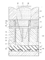
- FIG. 2 is a diagram showing a cross-sectional configuration of the solid-state imaging device taken along line AA of FIG. 1;
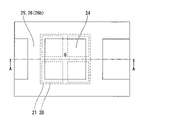
- FIG. 2B is a diagram showing a cross-sectional configuration of the solid-state imaging device taken along line BB of FIG. 2A;
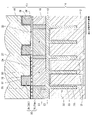
- FIG. 3 is a diagram showing the state of light in the solid-state imaging device according to the first embodiment;
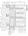
- It is a figure which shows the state of the light in the conventional solid-state imaging device.
- FIG. 1 It is a figure which shows the cross-sectional structure of the solid-state imaging device which concerns on a modification. It is a figure which shows the cross-sectional structure of the solid-state imaging device which concerns on a modification. It is a figure which shows the cross-sectional structure of the solid-state imaging device which concerns on a modification. It is a figure which shows the cross-sectional structure of the solid-state imaging device which concerns on a modification. It is a figure which shows the cross-sectional structure of the solid-state imaging device which concerns on a modification. It is a figure which shows the cross-sectional structure of the solid-state imaging device which concerns on a modification. It is a figure which shows the cross-sectional structure of the solid-state imaging device which concerns on a modification. It is a figure which shows the cross-sectional structure of the solid-state imaging device which concerns on a modification. FIG.
- 13B is a diagram showing a cross-sectional configuration of the solid-state imaging device taken along line CC of FIG. 13A; It is a figure which shows the cross-sectional structure of the solid-state imaging device which concerns on a modification. It is a figure which shows the cross-sectional structure of the solid-state imaging device which concerns on a modification. It is a figure which shows the cross-sectional structure of the solid-state imaging device which concerns on a modification. It is a figure which shows the cross-sectional structure of the solid-state imaging device which concerns on a modification. It is a figure which shows the cross-sectional structure of the solid-state imaging device which concerns on a modification.
- FIG. 13B is a diagram showing a cross-sectional configuration of a solid-state imaging device according to a modification, taken at a position corresponding to line CC in FIG. 13A;
- FIG. 13B is a diagram showing a cross-sectional configuration of a solid-state imaging device according to a modification, taken at a position corresponding to line CC in FIG. 13A;
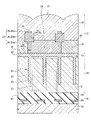
- FIG. 22B is a diagram showing a cross-sectional configuration of the solid-state imaging device taken along line DD of FIG.
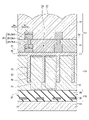
- FIG. 22A It is a figure which shows the cross-sectional structure of the solid-state imaging device which concerns on a modification.
- FIG. 23B is a diagram showing a cross-sectional configuration of the solid-state imaging device taken along line EE of FIG. 23A; It is a figure which shows the cross-sectional structure of the solid-state imaging device which concerns on a modification. It is a figure which shows the cross-sectional structure of the solid-state imaging device which concerns on a modification. It is a figure which shows the cross-sectional structure of the solid-state imaging device which concerns on a modification. It is a figure which shows the formation method of an upper stage partition layer. It is a figure which shows the formation method of an upper stage partition layer.
- FIG. 35B is a diagram showing a cross-sectional configuration of the solid-state imaging device taken along line FF of FIG. 35A; It is a figure which shows the cross-sectional structure of the solid-state imaging device which concerns on a modification. It is a figure which shows the cross-sectional structure of the solid-state imaging device which concerns on a modification.
- FIG. 35B is a diagram showing a cross-sectional configuration of the solid-state imaging device taken along line FF of FIG. 35A; It is a figure which shows the cross-sectional structure of the solid-state imaging device which concerns on a modification. It is a figure which shows the cross-sectional structure of the solid-state imaging device which concerns on a modification.
- FIG. 22B is a diagram showing a cross-sectional configuration of a solid-state imaging device according to a modification, taken at a position corresponding to line DD of FIG. 22A;
- FIG. 22B is a diagram showing a cross-sectional configuration of a solid-state imaging device according to a modification, taken at a position corresponding to line DD of FIG. 22A;
- 3 is a schematic configuration diagram of an electronic device according to a second embodiment;
- FIG. Embodiments of the present disclosure will be described in the following order. Note that the present disclosure is not limited to the following examples. Also, the effects described in this specification are examples and are not limited, and other effects may also occur.
- First Embodiment Solid-State Imaging Device 1-1 Overall Configuration of Solid-State Imaging Device 1-2 Configuration of Main Part 1-3 Modification 2. Second Embodiment: Example of Application to Electronic Equipment
- FIG. 1 is a schematic configuration diagram showing the entire solid-state imaging device 1 according to the first embodiment.
- the solid-state imaging device 1 of FIG. 1 is a back-illuminated CMOS (Complementary Metal Oxide Semiconductor) image sensor.
- CMOS Complementary Metal Oxide Semiconductor
- the solid-state imaging device 1 (1002) captures image light (incident light) from an object through a lens group 1001, and measures the amount of incident light formed on the imaging surface in units of pixels.
- the solid-state imaging device 1 includes a substrate 2, a pixel region 3, a vertical drive circuit 4, a column signal processing circuit 5, a horizontal drive circuit 6, an output circuit 7, and a control circuit 8. It has
- the pixel region 3 has a plurality of pixels 9 regularly arranged in a two-dimensional array on the substrate 2 .
- the pixel 9 has the photoelectric conversion unit 20 shown in FIG. 2A and a plurality of pixel transistors (not shown).
- a plurality of pixel transistors for example, four transistors, a transfer transistor, a reset transistor, a selection transistor, and an amplifier transistor, can be used as the plurality of pixel transistors.
- three transistors excluding the selection transistor may be employed.
- the vertical drive circuit 4 is composed of, for example, a shift register, selects a desired pixel drive wiring 10, supplies a pulse for driving the pixels 9 to the selected pixel drive wiring 10, and drives each pixel 9 in units of rows. drive. That is, the vertical drive circuit 4 sequentially selectively scans the pixels 9 in the pixel region 3 in the vertical direction row by row, and generates pixel signals based on signal charges generated by the photoelectric conversion units 20 of the pixels 9 according to the amount of received light. , to the column signal processing circuit 5 through the vertical signal line 11 .
- the column signal processing circuit 5 is arranged, for example, for each column of the pixels 9, and performs signal processing such as noise removal on signals output from the pixels 9 of one row for each pixel column.
- the column signal processing circuit 5 performs signal processing such as CDS (Correlated Double Sampling) and AD (Analog Digital) conversion for removing pixel-specific fixed pattern noise.
- the horizontal driving circuit 6 is composed of, for example, a shift register, sequentially outputs horizontal scanning pulses to the column signal processing circuits 5, selects each of the column signal processing circuits 5 in turn, and The pixel signal subjected to the signal processing is output to the horizontal signal line 12 .
- the output circuit 7 performs signal processing on pixel signals sequentially supplied from each of the column signal processing circuits 5 through the horizontal signal line 12 and outputs the processed pixel signals.
- signal processing for example, buffering, black level adjustment, column variation correction, and various digital signal processing can be used.
- the control circuit 8 generates a clock signal and a control signal that serve as references for the operation of the vertical drive circuit 4, the column signal processing circuit 5, the horizontal drive circuit 6, etc. based on the vertical synchronization signal, the horizontal synchronization signal, and the master clock signal. Generate. The control circuit 8 then outputs the generated clock signal and control signal to the vertical drive circuit 4, the column signal processing circuit 5, the horizontal drive circuit 6, and the like.
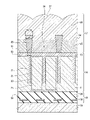
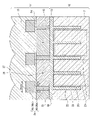
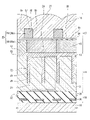
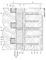
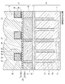
- FIG. 2A is a diagram showing a cross-sectional configuration of the solid-state imaging device 1 taken along line AA in FIG.
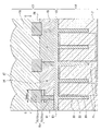
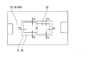
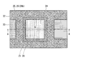
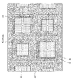
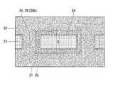
- FIG. 2B is a diagram showing a cross-sectional configuration of the solid-state imaging device 1 taken along line BB of FIG. 2A. Note that the microlenses 27 are omitted in FIG. 2B so that the color filters 24 are clearly visible.
- the solid-state imaging device 1 includes a light-receiving layer 14 formed by laminating a substrate 2 and an insulating film 13 in this order.
- a light collecting layer 17 is formed by laminating a color filter layer 15 and a microlens layer 16 in this order. .
- the color filter layer 15 is arranged between the substrate 2 and the microlens layer 16 .
- a wiring layer 18 and a support substrate 19 are laminated in this order on the surface of the light receiving layer 14 on the substrate 2 side (hereinafter also referred to as “surface S2").
- the back surface of the insulating film 13 is also referred to as “back surface S1”.
- the surface of the substrate 2 is also expressed as "surface S2".
- the substrate 2 is composed of a semiconductor substrate made of silicon (Si), for example, and forms a pixel region 3 .
- a plurality of pixels 9 including photoelectric conversion units 20 are arranged in a two-dimensional array in the pixel region 3 .
- Each of the photoelectric conversion units 20 is embedded in the substrate 2 to form a photodiode, generates signal charges according to the amount of incident light 28, and accumulates the generated signal charges.
- At least two adjacent photoelectric conversion units 20 constitute a photoelectric conversion unit group 21 .
- each of four photoelectric conversion units 20 adjacent in the row direction and the column direction constitutes the photoelectric conversion unit group 21 .
- the photoelectric conversion unit group 21 is composed of a plurality of photoelectric conversion units 20 .
- the photoelectric conversion unit group 21 is arranged in a two-dimensional array in the pixel region 3 .
- a pixel separation section 22 is formed between adjacent photoelectric conversion sections 20 .
- the pixel separation section 22 is formed in a lattice shape so as to surround each photoelectric conversion section 20 .
- the pixel separation portion 22 has a bottomed trench portion 23 (groove portion) formed in the depth direction from the side of the substrate 2 facing the insulating film 13 (hereinafter also referred to as “back surface S3”).
- the trench portion 23 is formed in a lattice shape so that the inner side surface and the bottom surface form the outer shape of the pixel separating portion 22 .
- An insulating film 13 covering the rear surface S3 side of the substrate 2 is embedded inside the trench portion 23 .
- the insulating film 13 continuously covers the entire rear surface S3 side of the substrate 2 (the entire light receiving surface side) and the inside of the trench portion 23 .
- an insulator can be used as the material of the insulating film 13 .
- silicon oxide (SiO 2 ) and silicon nitride (SiN) can be used.
- the color filter layer 15 has a plurality of color filters 24 formed on the back surface S1 side of the insulating film 13 and arranged corresponding to the photoelectric conversion unit group 21 . That is, each of the plurality of color filters 24 has a structure in which one color filter 24 is shared by four adjacent photoelectric conversion units 20 . Moreover, the plurality of color filters 24 include a plurality of types of color filters that transmit light of mutually different wavelengths (eg, red light, green light, and blue light). As a result, each of the plurality of color filters 24 transmits light of a predetermined wavelength for each type of color filter, and allows the transmitted light to enter the photoelectric conversion unit 20 . As the array pattern of the color filters 24, for example, a Bayer array can be adopted. As the material of the color filter 24, for example, a color resist having a refractive index of 1.4 to 1.9 can be used.
- a low refractive index layer 25 is formed between adjacent color filters 24 .
- the low refractive index layer 25 is formed on the back surface S1 side of the insulating film 13 in the same manner as the color filters 24, and is formed in a lattice shape so as to surround the color filters 24.
- the low refractive index layer 25 includes a plurality of partition layers 26 arranged in a direction perpendicular to the rear surface S3 (light receiving surface) of the substrate 2 .
- FIG. 2A illustrates a case where the low refractive index layer 25 is configured by laminating (integrating) the two-step partition wall layers 26 .
- Each of the plurality of partition layers 26 is formed in a grid pattern so as to form each part of the low refractive index layer 25 .
- the partition wall layer 26 on the substrate 2 side (hereinafter also referred to as “lower partition layer 26a”) is entirely present between the color filters 24, and the lower end thereof is the interface between the color filter 24 and the insulating film 13.
- the partition wall layer 26 on the microlens 27 side (hereinafter also referred to as “upper partition layer 26b”) protrudes into the microlens 27 on the microlens 27 side. That is, it can be said that at least a portion of the low refractive index layer 25 is arranged between the color filters 24 .
- the material of the partition wall layer 26 (that is, the material of the low refractive index layer 25), for example, a low refractive index material having a lower refractive index than the material of the adjacent layer (that is, the adjacent substance), or air can be adopted.
- the material of the adjacent layer is the material of the layer (substance in contact with the partition layer 26) in contact with the partition layer 26 in the direction parallel to S3 (light receiving surface) of the substrate 2.
- FIG. For example, the material of the color filter layer 15 and the material of the microlens layer 16 are listed.
- Low refractive index materials include, for example, low refractive index resins having a refractive index of 1.0 to 1.2.
- the color filter 24, the microlens 27, and the low refractive index layer 25 form a waveguide with the color filter 24 and the microlens 27 as a core and the low refractive index layer 25 as a clad.
- the surface of the partition layer 26 on the color filter 24 side extends in a direction perpendicular to the rear surface S3 (light receiving surface) of the substrate 2 . That is, in a cross section perpendicular to the back surface S3 (light receiving surface) of the substrate 2, the cross-sectional shape of the partition layer 26 is a rectangular shape with a constant width. Moreover, the partition layers 26 in adjacent steps have different widths.
- the width of the partition layer 26 is the width of the partition layer 26 in the direction parallel to the back surface S3 of the substrate 2 in the cross section perpendicular to the back surface S3 of the substrate 2 . Specifically, it can be said to be the width of the partition layer 26 in the direction passing through the centers of the adjacent color filters 24 .
- FIG. 2A illustrates the case where the width Wb of the upper partition layer 26b is wider than the width Wa of the lower partition layer 26a. That is, in a cross section perpendicular to the back surface S3 (light receiving surface) of the substrate 2, the cross-sectional shape of the low refractive index layer 25 is T-shaped.
- the low refractive index layer 25 has a width Wb (in a broad sense, “first width Wwide”) on the side of the microlens 27 and a width narrower than the width Wb on the side of the substrate 2 with respect to the portion having the width Wb.
- Wa in a broad sense, “second width Wmin”).
- the width Wb of the upper partition layer 26b and the width Wa of the lower partition layer 26a are set so as to satisfy the following formula (1). 1.0 ⁇ Wb/Wa ⁇ 15.0 (1)
- the width-to-height ratio of the partition layer 26 is not particularly limited.
- the microlens layer 16 is formed on the back surface S4 side (light receiving surface side) of the color filter layer 15 and has a plurality of microlenses 27 arranged corresponding to the photoelectric conversion unit group 21 . That is, each of the plurality of microlenses 27 has a structure in which one microlens 27 is shared by four adjacent photoelectric conversion units 20 . As a result, each of the microlenses 27 converges the image light (incident light 28) from the subject, and the condensed incident light 28 is composed of the color filter 24, the microlens 27, and the low refractive index layer 25. It is guided into the photoelectric conversion section 20 via the waveguide.
- FIG. 2A illustrates a case where the microlens 27 is misaligned and the center of the microlens 27 is shifted from the center of the photoelectric conversion unit group 21 .
- the wiring layer 18 is formed on the surface S2 side of the substrate 2 and includes an interlayer insulating film 29 and wirings 30 laminated in multiple layers with the interlayer insulating film 29 interposed therebetween.
- the wiring layer 18 drives the pixel transistors forming each pixel 9 through multiple layers of wiring 30 .
- the support substrate 19 is formed on the surface of the wiring layer 18 opposite to the side facing the substrate 2 .
- the support substrate 19 is a substrate for securing the strength of the substrate 2 in the manufacturing stage of the solid-state imaging device 1 . Silicon (Si), for example, can be used as the material of the support substrate 19 .
- the solid-state imaging device 1 having the above configuration, light is irradiated from the rear surface S3 side of the substrate 2 (the rear surface S1 side of the light-receiving layer 14), and the irradiated light is transmitted through the microlenses 27 and the color filters 24 (waveguides). Then, the transmitted light is photoelectrically converted by the photoelectric conversion unit 20 to generate signal charges. The generated signal charges are output as pixel signals through the vertical signal lines 11 of FIG.
- one microlens 27 is shared by at least two or more adjacent photoelectric conversion units 20 (photoelectric conversion unit group 21)
- the number of microlenses included in the photoelectric conversion unit group 21 depends on the distance to the subject. A difference occurs between the signal charges of the photoelectric conversion unit 20 that are connected. Therefore, the solid-state imaging device 1 can calculate the distance to the object based on the difference between the signal charges.
- the center of the microlens 27 deviates from the center of the photoelectric conversion unit group 21 in plan view, and the center of the condensed spot 31 of the incident light 28 by the microlens 27 and the photoelectric conversion unit group. There was a possibility that the center of 21 was shifted.
- a low refractive index layer 25 containing air or a material having a lower refractive index than the material of the adjacent layers is formed between the color filters 24 .
- the low refractive index layer 25 has a width Wb (first width Wwide) on the microlens 27 side and a width Wa (second width Wwide) narrower than the width Wb on the substrate 2 side from the portion having the width Wb. Wmin).
- the width Wb of the portion of the low refractive index layer 25 on the side of the microlens 27 of the portion of the incident light 28 deviating from the center of the photoelectric conversion portion group 21 among the incident light 28 that has passed through the microlenses 27 is widened.
- the light hits the low refractive index layer 25 and is diffracted toward the center of the color filter 24 .
- the refractive index of the material of the low refractive index layer 25 is low, and the low refractive index layer 25 makes it difficult for light to propagate. Incident light 28 is diffracted so as to avoid layer 25 .
- the incident light 28 striking the upper surface of the low refractive index layer 25 on the right side is diffracted, and the diffracted incident light 28 travels from the side surface of the low refractive index layer 25 toward the center of the photoelectric conversion portion group 21.
- the position of the focused spot 31 can be moved to the vicinity of the center in the width direction of the color filter 24 and closer to the microlens side in the height direction of the color filter 24 than in FIG. Part of the incident light 28 is transmitted through the low refractive index layer 25 .
- the incident light 28 passing through the focused spot 31 near the center of the color filter 24 spreads over a wide range because the width Wa of the portion of the low refractive index layer 25 on the substrate 2 side is narrow.
- the incident light 28 can be spread within the photoelectric conversion section 20 . Therefore, it is possible to suppress the bias in the light receiving sensitivity between the photoelectric conversion units 20 and reduce the difference in light receiving sensitivity between the photoelectric conversion units 20 . Therefore, according to the solid-state imaging device 1 of the first embodiment, the same-color sensitivity difference can be reduced.
- the traveling direction of the incident light 28 is tilted with respect to the back surface S3 (light receiving surface) of the substrate 2, the traveling direction of the incident light 28 is The portion on the side opposite to the tilt direction (right side in FIG. 4) strikes the low refractive index layer 25 on the side opposite to the tilt direction in the traveling direction (right side in FIG. 4) and is diffracted toward the center side of the color filter 24 . Therefore, the position of the focused spot 31 can be moved closer to the microlens side in the height direction of the color filter 24 than in FIG. 3, and can be moved toward the tilt direction of the incident light 28 (left side in FIG. 4). .
- the incident light 28 that has passed through the condensed spot 31 can be biased toward the tilt direction side (left side in FIG. 4) inside the color filter 24 and the photoelectric conversion section 20 . Therefore, the light receiving sensitivity difference between the photoelectric conversion units 20 can be increased. Therefore, according to the solid-state imaging device 1 of the first embodiment, the separation ratio can be improved.
- FIG. 4 illustrates the case where the center of the microlens 27 is displaced from the center of the photoelectric conversion unit group 21, the effect of improving the separation ratio can be obtained even when it is not displaced.
- the traveling direction of the incident light 28 is inclined with respect to the back surface S3 (light receiving surface) of the substrate 2.
- the portion of the incident light 28 on the side opposite to the direction of inclination of the traveling direction (right side in FIG. 5) hits the low refractive index layer 25 on the side opposite to the direction of inclination of the traveling direction (right side in FIG. 5).
- the condensed spot 31 is closer to the rear surface S3 (light receiving surface) than in FIG. Therefore, compared to the solid-state imaging device 1 of the first embodiment, the light receiving sensitivity difference between the photoelectric conversion units 20 is small, and the separation ratio is deteriorated.
- the low refractive index layer 25 includes three partition layers 26, and in addition to the lower partition layer 26a and the upper partition layer 26b shown in FIG. 26 (hereinafter also referred to as “uppermost partition wall layer 26c”) are stacked to constitute the low refractive index layer 25.
- the width Wc of the uppermost partition layer 26c is narrower than the width Wb of the upper partition layer 26b, and is the same as the width Wa of the lower partition layer 26a.
- the low refractive index layer 25 includes three partition layers 26, the width Wf of the partition wall layer 26 closest to the microlens (hereinafter also referred to as the "upper partition layer 26f") and the width Wf of the partition wall layer 26 closest to the substrate 2.
- the cross-sectional shape of the low refractive index layer 25 is I-shaped.
- the width Wf of the upper partition layer 26f becomes the "first width Wwide”.
- the width We of the middle partition layer 26e becomes the "second width Wmin”. 8
- the sum of the height of the middle partition layer 26e and the height of the lower partition layer 26d is equal to the height of the color filter 24, and the entire upper partition layer 26f is within the microlens 27.
- the lower partition layer 26a and the upper partition layer 26b are stacked (in contact with each other), but other configurations may be employed.
- one stage of the partition wall layer 26 and the other stage of the partition layer 26 adjacent to the one stage of the partition layer 26 among the plurality of stages of the partition wall layers 26 are mutually arranged. It is good also as a structure which is spaced apart.
- FIG. 9 illustrates a case where the low refractive index layer 25 includes two partition layers 26 (a lower partition layer 26a and an upper partition layer 26b), and the lower partition layer 26a and the upper partition layer 26b are separated from each other.
- the width of the lower partition layer 26a and the width of the upper partition layer 26b are set to be constant, but other configurations may be employed.
- the width Wb of the upper partition wall layer 26b may be configured such that the width Wb increases continuously toward the microlens 27 side (the light receiving surface side of the microlens 27). That is, in a cross section perpendicular to the back surface S3 (light receiving surface) of the substrate 2, the cross-sectional shape of the low refractive index layer 25 may be a shape in which a trapezoid whose upper base is wider than its lower base and a rectangle are combined in series. In this case, as shown in FIG.
- the low refractive index layer 25 may have a configuration in which the width W continuously increases toward the microlens 27 over the entire low refractive index layer 25 . That is, in a cross section perpendicular to the rear surface S3 (light receiving surface) of the substrate 2, the cross-sectional shape of the low refractive index layer 25 may be a trapezoid whose upper base is wider than its lower base.
- the width W of the end portion of the low refractive index layer 25 on the microlens 27 side is the "first width Wwide”
- the width W of the end portion on the substrate 2 side is the "second width Wwide”. width Wmin”.
- the same material is used for the lower partition layer 26a and the upper partition layer 26b, and the inside of the low refractive index layer 25 has a constant refractive index.
- the low refractive index layer 25 may have a different refractive index for each height position in the low refractive index layer 25 .
- the height position in the low refractive index layer 25 is the height position in the low refractive index layer 25 from the back surface S3 of the substrate 2 in the direction perpendicular to the back surface S3 (light receiving surface) of the substrate 2. .
- a low refractive index resin is used as the material of the lower partition wall layer 26a
- air is used as the material of the upper partition wall layer 26b
- the lower partition wall layer 26a and the upper partition wall layer 26b have different refractive indexes. exemplified.
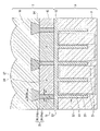
- FIGS. 13A and 13B show the case of application to the solid-state imaging device 1 shown in FIGS. 2A and 2B.
- FIGS. 14, 15, 16, 17 and 18 each illustrate the case of application to the solid-state imaging device 1 shown in FIGS. 8, 9, 10, 11 and 12. there is 13A and FIGS.
- the width direction protrusion amounts Or, Og, and Ob of the portion of the low refractive index layer 25 having the first width Wwide (upper partition wall layer 26b) toward the color filter 24 side are 10 illustrates a case in which the configuration is different for each type of color filter 24 to which the .
- the amount of protrusion in the width direction Or to the color filter 24 that transmits red light the amount of protrusion in the width direction Ob to the color filter 24 that transmits blue light > the amount of protrusion in the width direction to the color filter 24 that transmits green light Og It has become.
- the focused spot 31 can be formed at a more appropriate position.
- the low refractive index layer 25 may be arranged at a pupil-corrected position.
- FIG. 19 illustrates a case in which the upper partition layer 26b is arranged at a pupil-corrected position. That is, from the center to the end of the pixel region 3, the straight line portions forming the lattice of the upper partition layer 26b are closer to the pixel region 3 than the straight line portions forming the lattice of the pixel separating portion 22 in plan view.
- the correction amounts of the color filter 24, the lower partition layer 26a, the upper partition layer 26b, and the microlenses 27 may be different from each other.
- the photoelectric conversion unit group 21 may be composed of two 2 ⁇ 1 photoelectric conversion units 20 .
- FIG. 20 illustrates a case where each of two photoelectric conversion units 20 adjacent to each other in the row direction constitutes the photoelectric conversion unit group 21 . Accordingly, a structure in which one color filter 24 or one microlens 27 is shared by two adjacent photoelectric conversion units 20 can be provided.
- the configuration of the photoelectric conversion unit group 21 shown in FIG. 20 can also be applied to the solid-state imaging device 1 shown in FIGS. Further, for example, when applied to the solid-state imaging device 1 shown in FIGS. 13A to 18, as shown in FIG. FIG. 21 shows only “Og”) may be changed at each part of the low refractive index layer 25 surrounding one color filter 24 .
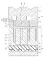
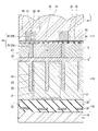
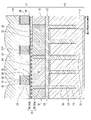
- a configuration may be provided in which a protective film 32 is arranged between the upper partition layer 26b and the microlens 27 to cover the upper partition layer 26b.
- the protective film 32 covers the width direction side surfaces of the upper partition wall layer 26b (hereinafter also referred to as “side surfaces S5 and S6”) and the surface opposite to the color filter 24 side surface (hereinafter also referred to as “back surface S7”). ) and only.
- the protective film 32 for example, a film that prevents the material of the microlenses 27 from entering (permeating) into the upper partition wall layer 26b can be used.
- a material that prevents the material of the microlenses 27 from passing through can be used.
- examples thereof include LTO (Low Temperature Oxide) films such as silicon oxide films and silicon nitride films. This can prevent the material of the microlenses 27 (transparent resin with a relatively high refractive index) from soaking into the material of the upper partition wall layer 26b (low refractive index resin with a relatively low refractive index). An increase in the refractive index of the material (low refractive index resin) can be suppressed. Therefore, the focused spot 31 can be formed at a more appropriate position.
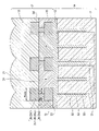
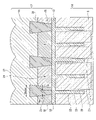
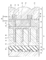
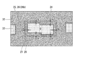
- FIG. 22B is a diagram showing a cross-sectional configuration of the solid-state imaging device 1 taken along line DD in FIG. 22A. Note that the microlenses 27 are omitted in FIG. 22B so that the protective film 32 can be clearly seen.
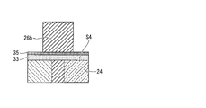
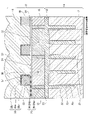
- the lower partition layer 26a is wholly present between the color filters 24, and the upper partition layer 26b is present closer to the microlenses 27 than the rear surface S4 (light receiving surface) of the color filter 24.
- a stopper film hereinafter referred to as “first stopper film 33” is arranged on the back surface S4 (light receiving surface) of the color filter 24 and covers the entire back surface S4 (light receiving surface) of the color filter 24. also called).
- the upper partition wall layer 26b is arranged on the light receiving surface (hereinafter also referred to as “back surface S8”) of the first stopper film 33 while being covered with the protective film 32 .
- the first stopper film 33 for example, a film that functions as an etching stopper can be used.
- a material with a low etching rate can be used.
- titanium oxide (TiO 2 ) can be mentioned.
- layers made of the materials of the first stopper film 33 and the protective film 32 are formed in this order on the rear surface S4 of the color filter 24 .
- dry etching is performed to form the upper partition layer 26b. In such a procedure, according to the solid-state imaging device 1 shown in FIG. 22A, etching can be stopped by the first stopper film 33, and the color filter 24 can be prevented from being etched.
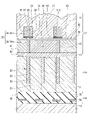
- FIGS. 23A and 23B in the solid-state imaging device 1 shown in FIGS. It may be arranged between the upper partition layers 26b to continuously cover the plurality of upper partition layers 26b.
- FIG. 23A for each of the plurality of upper partition wall layers 26b arranged on the first stopper film 33 (back surface S8), the side surfaces S5 and S6 and the rear surface S7 of the plurality of upper partition wall layers 26b and the first stopper film are formed.
- 33 illustrates the case where the protective film 32 is arranged so as to continuously cover the area where the upper partition layer 26b does not exist in the rear surface S8 of the substrate 33.
- FIG. 23B is a diagram showing a cross-sectional configuration of the solid-state imaging device 1 taken along line EE of FIG. 23A. Note that the microlenses 27 are omitted in FIG. 23B so that the protective film 32 can be clearly seen.
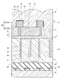
- the protective film 32 is arranged between the upper partition layer 26b and the microlens 27 to may be configured to cover only the rear surface S7 (the surface opposite to the surface on the side of the color filter 24).
- the microlenses 27 are formed on the portion of the upper partition wall layer 26b (low refractive index resin having a relatively low refractive index) which is hit by the incident light 28 shown in FIG. Infiltration of the material (transparent resin with a relatively high refractive index) can be suppressed.
- the protective film 32 is omitted from the solid-state imaging device 1 shown in FIGS.
- a configuration including only the first stopper film 33 may be employed.
- 25 illustrates the case where the upper partition layer 26b is arranged on the rear surface S8 of the first stopper film 33. As shown in FIG.
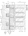
- a second stopper film 34 may be provided to cover only the portion of the rear surface S8 (light receiving surface) of 33 facing the upper partition wall layer 26b.
- the first stopper film 33 is arranged on the back surface S4 (on the light receiving surface) of the color filter 24 and covers the entire back surface S4 (light receiving surface) of the color filter 24 .
- the upper partition layer 26b is arranged on the light receiving surface (hereinafter also referred to as “back surface S9”) of the second stopper film 34 .
- Silicon oxynitride (SiON) for example, can be used as the material of the second stopper film 34 .
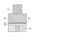
- FIG. 27B when forming the upper partition layer 26b, first, as shown in FIG. A layer 36 made of a material and an etching mask 37 made of a resist are formed in this order. Subsequently, as shown in FIG. 27B, dry etching is performed to form the upper partition layer 26b, as shown in FIG. 27C, ashing is performed to remove the etching mask 37, and as shown in FIG. A second stopper film 34 is formed by an electron beam (EB).
- EB electron beam
- the second stopper film 34 is arranged on the rear surface S8 (on the light receiving surface) of the first stopper film 33. It may be configured such that the back surface S8 (light receiving surface) of the first stopper film 33 is entirely covered.
- the first stopper film 33 is arranged on the back surface S4 (on the light receiving surface) of the color filter 24 and covers the entire back surface S4 (light receiving surface) of the color filter 24 .
- the upper partition layer 26b is arranged on the back surface S9 of the second stopper film 34 (on the light receiving surface).
- the solid-state imaging device 1 shown in FIG. 26 may be configured to include a protective film 32 covering the upper partition wall layer 26b.
- the first stopper film 33 is arranged on the back surface S4 (on the light receiving surface) of the color filter 24 to cover the entire back surface S4 (light receiving surface) of the color filter 24 .
- a second stopper film 34 is arranged on the rear surface S8 (on the light receiving surface) of the first stopper film 33, and covers only the portion facing the upper partition layer 26b.
- the upper partition layer 26b is arranged on the rear surface S9 (on the light receiving surface) of the second stopper film 34 while being covered with the protective film 32 . This can prevent the material of the microlenses 27 from soaking into the material of the upper partition layer 26b, and can prevent the material (low refractive index resin) of the upper partition layer 26b from increasing in refractive index.
- the solid-state imaging device 1 shown in FIG. A configuration including a protective film 32 covering only the surface opposite to the surface S10 may be provided.
- the upper partition wall layer 26b is arranged on the rear surface S9 (on the light receiving surface) of the second stopper film 34 while being covered with the protective film 32 .
- the material of the microlenses 27 transparent resin with a relatively high refractive index
- the first stopper film 33 is arranged on the back surface S4 (on the light receiving surface) of the color filter 24 and covers the entire back surface S4 (light receiving surface) of the color filter 24.
- the second stopper film 34 is arranged on the back surface S8 (on the light receiving surface) of the first stopper film 33 to cover the entire back surface S8 (light receiving surface) of the first stopper film 33 .
- the upper partition layer 26b is arranged on the rear surface S9 (light receiving surface) of the second stopper film 34 while being covered with the protective film 32 .
- the first stopper film 33 is arranged on the back surface S4 (on the light receiving surface) of the color filter 24 to cover the entire back surface S4 (light receiving surface) of the color filter 24.
- a protective film 32 is disposed between the upper partition layer 26b and the microlens 27 to cover the upper partition layer 26b. In the protective film 32, the material of the first portion 32a and the material of the second portion 32b are different.
- the material of the first portion 32a examples include an LTO film.
- silicon oxynitride (SiON), for example, can be used as the material of the second portion 32b.
- the first portion 32a and the second portion 32b may be made of the same material.
- the first portion 32a may be any portion of the protective film 32, and the second portion 32b may be any portion different from the first portion 32a.
- the portion of the protective film 32 on the back surface S7 side of the upper partition layer 26b has a two-layer structure, and the portion on the lower layer side has a first layer structure. portion 32a, and the remaining portion including the portion on the upper layer side may be the second portion 32b.
- the first stopper film 33 is arranged on the back surface S4 (on the light receiving surface) of the color filter 24 to cover the entire back surface S4 (light receiving surface) of the color filter 24.
- a protective film 32 is disposed between the upper partition wall layer 26b and the microlens 27 and between the plurality of upper partition wall layers 26b to continuously cover the plurality of upper partition wall layers 26b.
- the first portion 32a and the second portion 32b may be made of the same material, or may be configured so that other factors such as film thickness are separately produced.
- FIG. 34 is a diagram showing a case where the first stopper film 33 is omitted from the configuration of FIG. 22A.
- the width of the low-refractive-index layer 25 may be changed asymmetrically in the left-right, up-down, or right-left direction depending on the height.
- 35A and 35B show the case of application to the solid-state imaging device 1 shown in FIGS. 22A and 22B.
- the width direction projection amounts Or, Og, and Ob of the portion of the low refractive index layer 25 having the first width Wwide (upper partition wall layer 26b) toward the color filter 24 side are defined by the colors to which the portions project.
- a case is illustrated in which the configuration is different for each type of filter 24 .
- FIG. 35B is a diagram showing a cross-sectional configuration of the solid-state imaging device 1 taken along line FF of FIG. 35A. Note that the microlenses 27 are omitted in FIG. 35B so that the first stopper film 33 can be clearly seen.
- FIG. 36 shows a case of application to the solid-state imaging device 1 shown in FIG. 22A.
- FIGS. 37, 38, 39, 40, 41, 42, 43, 44, 45, and 46 correspond to FIGS. 23A, 24, 25, 26, and 28, respectively. , 29, 30, 31, 32, and 33 are illustrated.
- the upper partition wall layer 26b is arranged at a pupil-corrected position.
- the straight line portions forming the lattice of the upper partition layer 26b are closer to the pixel region 3 than the straight line portions forming the lattice of the pixel separating portion 22 in plan view. shifted toward the center of the By arranging them at the pupil-corrected positions, it is possible to suppress unevenness in light receiving sensitivity among the photoelectric conversion units 20 included in the photoelectric conversion unit group 21 on the end portion side (high image height side) of the pixel region 3, and photoelectric conversion.
- the light receiving sensitivity difference (sensitivity difference between the same colors) between the portions 20 can be reduced.
- the correction amount of the color filter 24, the correction amount of the lower partition layer 26a, the correction amount of the upper partition layer 26b, and the correction amount of the microlens 27 may be different from each other.
- FIG. 47 illustrates a case in which two photoelectric conversion units 20 adjacent to each other and arranged in the row direction (horizontal direction in FIG. 47) respectively constitute the photoelectric conversion unit group 21 . Accordingly, a structure in which one color filter 24 or one microlens 27 is shared by two adjacent photoelectric conversion units 20 can be provided.
- the configuration of the photoelectric conversion unit group 21 shown in FIG. 47 can also be applied to the solid-state imaging device 1 shown in FIGS. Further, for example, when applied to the solid-state imaging device 1 shown in FIGS. 36 to 45, as shown in FIG. Only “Og” is shown in FIG. 48) may be changed at each part of the low refractive index layer 25 surrounding one color filter 24 .
- the present technology can also be applied to light detection devices in general, including a distance measuring sensor that measures distance, also called a ToF (Time of Flight) sensor.
- a ranging sensor emits irradiation light toward an object, detects the reflected light that is reflected from the surface of the object, and then detects the reflected light from the irradiation light until the reflected light is received. It is a sensor that calculates the distance to an object based on time.
- the light-receiving pixel structure of this distance measuring sensor the structure of the pixel 9 described above can be adopted.
- FIG. 49 is a diagram showing an example of a schematic configuration of an imaging device (video camera, digital still camera, etc.) as an electronic device to which the present disclosure is applied.
- an imaging device 1000 includes a lens group 1001, a solid-state imaging device 1002 (the solid-state imaging device 1 according to the first embodiment), a DSP (Digital Signal Processor) circuit 1003, and a frame memory 1004. , a monitor 1005 and a memory 1006 .
- DSP circuit 1003 , frame memory 1004 , monitor 1005 and memory 1006 are interconnected via bus line 1007 .
- a lens group 1001 guides incident light (image light) from a subject to a solid-state imaging device 1002 and forms an image on a light receiving surface (pixel area) of the solid-state imaging device 1002 .
- the solid-state imaging device 1002 consists of the CMOS image sensor of the first embodiment described above.
- the solid-state imaging device 1002 converts the amount of incident light imaged on the light-receiving surface by the lens group 1001 into an electric signal for each pixel, and supplies the signal to the DSP circuit 1003 as a pixel signal.
- the DSP circuit 1003 performs predetermined image processing on pixel signals supplied from the solid-state imaging device 1002 . Then, the DSP circuit 1003 supplies the image signal after the image processing to the frame memory 1004 on a frame-by-frame basis, and temporarily stores it in the frame memory 1004 .
- the monitor 1005 is, for example, a panel type display device such as a liquid crystal panel or an organic EL (Electro Luminescence) panel.
- a monitor 1005 displays an image (moving image) of a subject based on the pixel signals for each frame temporarily stored in the frame memory 1004 .
- the memory 1006 consists of a DVD, flash memory, or the like. The memory 1006 reads out and records the pixel signals for each frame temporarily stored in the frame memory 1004 .
- Electronic equipment to which the solid-state imaging device 1 can be applied is not limited to the imaging device 1000, and can be applied to other electronic equipment. Further, although the solid-state imaging device 1 according to the first embodiment is used as the solid-state imaging device 1002, other configurations can also be adopted. For example, a configuration using another photodetector to which the present technology is applied, such as the solid-state imaging device 1 according to the modified example of the first embodiment, may be employed.
- the present technology can also take the following configuration.
- a substrate having a plurality of photoelectric conversion units arranged in a two-dimensional array; a microlens layer disposed on the light-receiving surface side of the substrate and including a plurality of microlenses formed for a photoelectric conversion unit group including at least two adjacent photoelectric conversion units; a color filter layer disposed between the substrate and the microlens layer and including a plurality of color filters for transmitting light of a predetermined wavelength component included in the light condensed by the microlens;
- a low refractive index layer containing air or a low refractive index material having a lower refractive index than the material of the adjacent layer, at least a part of which is disposed between the color filters;
- the low refractive index layer has a first width on the microlens side and a second width narrower than the first width on the substrate side of the portion having the first width.
- this (1) is "A substrate having a plurality of photoelectric conversion units arranged in a two-dimensional array, a microlens layer disposed on the light-receiving surface side of the substrate and including a plurality of microlenses formed for a photoelectric conversion unit group including at least two adjacent photoelectric conversion units; a color filter layer disposed between the substrate and the microlens layer and including a plurality of color filters for transmitting light of a predetermined wavelength component included in the light condensed by the microlens; a low refractive index layer at least partially disposed between the color filters;
- the low refractive index layer contains air or a low refractive index material having a lower refractive index than a substance in contact with the refractive index layer in a direction parallel to the light-receiving surface of the substrate.
- a photodetector having a first width and a second width narrower than the first width closer to the substrate than a portion having the first width. ' can also be said.
- the low refractive index layer includes the partition layer in two stages, The width of the upper partition layer, which is the partition wall layer in the step on the microlens side, is wider than the width of the lower partition layer, which is the partition wall layer in the step on the substrate side.
- a first stopper film disposed on the light-receiving surface of the color filter and covering the entire light-receiving surface of the color filter;
- the photodetector according to (6) wherein the upper partition layer is arranged on the light receiving surface of the first stopper film while being covered with the protective film.
- the photodetector according to (5) further comprising a protective film disposed between the upper partition layer and the microlens and between the plurality of upper partition layers to continuously cover the plurality of upper partition layers. .
- a first stopper film disposed on the light-receiving surface of the color filter and covering the entire light-receiving surface of the color filter; a second stopper film disposed on the light-receiving surface of the first stopper film and covering only a portion facing the upper partition layer; a protective film that covers only the surface of the upper partition layer on the color filter side and the surface opposite to the surface;
- a first stopper film disposed on the light-receiving surface of the color filter and covering the entire light-receiving surface of the color filter; a second stopper film disposed on the light receiving surface of the first stopper film and covering the entire light receiving surface of the first stopper film; a protective film that covers only the surface of the upper partition layer on the color filter side and the surface opposite to the surface;
- the photodetector according to (5) wherein the upper partition layer is arranged on the light receiving surface of the second stopper film while being covered with the protective film.
- the photodetector according to (6) wherein a first portion of the protective film and a second portion different from the first portion are separately formed.
- the photodetector according to (8) wherein a first portion of the protective film and a second portion different from the first portion are separately formed.
- the low refractive index layer includes three stages of the partition layer, The width of the partition layer in the step closest to the microlens and the width of the partition layer in the step closest to the substrate are wider than the width of the partition layer in the step therebetween. 3.
- Device. (25) A substrate having a plurality of photoelectric conversion portions arranged in a two-dimensional array, and a micrometer formed for a photoelectric conversion portion group consisting of at least two adjacent photoelectric conversion portions arranged on the light receiving surface side of the substrate.
- a microlens layer including a plurality of lenses
- a color filter layer disposed between the substrate and the microlens layer, the color filter layer including a plurality of color filters that transmit light of a predetermined wavelength component included in the light condensed by the microlenses
- a low refractive index layer containing air or a low refractive index material having a lower refractive index than the material of the adjacent layer, at least a part of which is disposed between the color filters, and the low refractive index layer includes the microlens and a photodetector having a second width narrower than the first width on the substrate side of a portion having the first width.
Landscapes
- Physics & Mathematics (AREA)
- Engineering & Computer Science (AREA)
- Multimedia (AREA)
- Signal Processing (AREA)
- General Physics & Mathematics (AREA)
- Optics & Photonics (AREA)
- Solid State Image Pick-Up Elements (AREA)
- Transforming Light Signals Into Electric Signals (AREA)
Abstract
Description
1-1 固体撮像装置の全体の構成
1-2 要部の構成
1-3 変形例
2.第2の実施形態:電子機器への応用例
[1-1 固体撮像装置の全体の構成]
本開示の第1の実施形態に係る固体撮像装置1(広義には「光検出装置」)について説明する。図1は、第1の実施形態に係る固体撮像装置1の全体を示す概略構成図である。
図1の固体撮像装置1は、裏面照射型のCMOS(Complementary Metal Oxide Semiconductor)イメージセンサである。図49に示すように、固体撮像装置1(1002)はレンズ群1001を介して、被写体からの像光(入射光)を取り込み、撮像面上に結像された入射光の光量を画素単位で電気信号に変換して画素信号として出力する。
図1に示すように、固体撮像装置1は、基板2と、画素領域3と、垂直駆動回路4と、カラム信号処理回路5と、水平駆動回路6と、出力回路7と、制御回路8とを備えている。
水平駆動回路6は、例えば、シフトレジスタによって構成され、水平走査パルスをカラム信号処理回路5に順次出力して、カラム信号処理回路5の各々を順番に選択し、カラム信号処理回路5の各々から信号処理が行われた画素信号を水平信号線12に出力させる。
制御回路8は、垂直同期信号、水平同期信号、及びマスタクロック信号に基づいて、垂直駆動回路4、カラム信号処理回路5、及び水平駆動回路6等の動作の基準となるクロック信号や制御信号を生成する。そして、制御回路8は、生成したクロック信号や制御信号を、垂直駆動回路4、カラム信号処理回路5、及び水平駆動回路6等に出力する。
次に、図1の固体撮像装置1の詳細構造について説明する。図2Aは、図1のA-A線で破断した場合の、固体撮像装置1の断面構成を示す図である。図2Bは、図2AのB-B線で破断した場合の、固体撮像装置1の断面構成を示す図である。なお、図2Bでは、カラーフィルタ24が明確となるように、マイクロレンズ27を省略している。
図2Aに示すように、固体撮像装置1は、基板2及び絶縁膜13がこの順に積層されてなる受光層14を備えている。また、受光層14の絶縁膜13側の面(以下、「裏面S1」とも呼ぶ)には、カラーフィルタ層15及びマイクロレンズ層16がこの順に積層されてなる集光層17が形成されている。換言すると、カラーフィルタ層15は、基板2とマイクロレンズ層16との間に配置されている、と言える。さらに、受光層14の基板2側の面(以下、「表面S2」とも呼ぶ)には、配線層18及び支持基板19がこの順に積層されている。なお、以下の記載では、絶縁膜13の裏面についても「裏面S1」と表す。また、基板2の表面についても「表面S2」と表す。
光電変換部20は、隣接する少なくとも2以上の光電変換部20で光電変換部群21を構成している。第1の実施形態では、光電変換部群21は、図2Bに示すように、2×2の4つの光電変換部20で構成されている。図2Bでは、行方向及び列方向に並び、隣接する4つの光電変換部20それぞれが光電変換部群21を構成する場合を例示している。また、光電変換部群21は、すべての光電変換部20を用いて複数構成されている。これにより、光電変換部群21は、画素領域3に二次元アレイ状に配置されている。
絶縁膜13は、基板2の裏面S3側全体(受光面側全体)、及びトレンチ部23の内部を連続的に被覆している。絶縁膜13の材料としては、例えば、絶縁物を用いることができる。具体的には、シリコン酸化物(SiO2)、シリコン窒化物(SiN)を採用できる。
隔壁層26の材料(即ち、低屈折率層25の材料)としては、例えば、隣接している層の材料(即ち、隣接している物質)よりも屈折率の低い低屈折率材料、又は空気を採用できる。隣接している層の材料としては、基板2のS3(受光面)と平行な方向において、隔壁層26に接している層の材料(隔壁層26に接している物質)である。例えば、カラーフィルタ層15の材料、マイクロレンズ層16の材料が挙げられる。また、低屈折率材料としては、例えば、屈折率1.0~1.2の低屈折率樹脂が挙げられる。これにより、カラーフィルタ24とマイクロレンズ27と低屈折率層25とは、カラーフィルタ24とマイクロレンズ27をコアとし、低屈折率層25をクラッドとして、導波路を形成する。
1.0<Wb/Wa≦15.0 …(1)
なお、隔壁層26の幅と高さとの比率は、特に限定されるものではない。
支持基板19は、配線層18の基板2に面する側とは反対側の面に形成されている。支持基板19は、固体撮像装置1の製造段階において、基板2の強度を確保するための基板である。支持基板19の材料としては、例えば、シリコン(Si)を用いることができる。
また、隣接した少なくとも2以上の光電変換部20(光電変換部群21)に対して、1つのマイクロレンズ27を共用する構造としたため、被写体までの距離に応じて、光電変換部群21に含まれる光電変換部20の信号電荷間に差が生じる。それゆえ、固体撮像装置1では、この信号電荷間の差を基に、被写体までの距離を算出可能となっている。
また、カラーフィルタ24の中央付近の集光スポット31を通過した入射光28は、低屈折率層25の基板2側の部分の幅Waが狭くなっていることで、広範囲に広がる。それゆえ、光電変換部20内において入射光28を広げることができる。そのため、光電変換部20間の受光感度の偏りを抑制でき、光電変換部20間において受光感度差を低減できる。したがって、第1の実施形態の固体撮像装置1によれば同色間感度差を低減できる。
なお、図4では、マイクロレンズ27の中心が光電変換部群21の中心からずれている場合を例示したが、ずれていない場合にも、分離比率の改善の効果を得ることができる。
(1)なお、第1の実施形態では、上段隔壁層26bのマイクロレンズ27側の部分がマイクロレンズ内に突出している例を示したが、他の構成を採用してもよい。例えば、図6に示すように、下段隔壁層26aが、その全体がカラーフィルタ24間に存在し、上段隔壁層26bが、カラーフィルタ24の裏面S4(受光面)よりもマイクロレンズ27側に存在している構成としてもよい。図6では、上段隔壁層26bと下段隔壁層26aとの境界がマイクロレンズ27とカラーフィルタ24との界面と同一面内に位置し、上段隔壁層26bは、その全体がマイクロレンズ27内に存在している場合を例示している。これにより、例えば、上段隔壁層26bがカラーフィルタ24間とマイクロレンズ27内とに跨って存在している場合に比べ、上段隔壁層26b(低屈折率層25)を作製しやすい。
この場合、図8に示すように、上段隔壁層26fの幅Wfが「第1の幅Wwide」となる。また、中段隔壁層26eの幅Weが「第2の幅Wmin」となる。また、図8では、中段隔壁層26eの高さと下段隔壁層26dの高さとの合計が、カラーフィルタ24の高さと等しくなっており、上段隔壁層26f全体がマイクロレンズ27内に入っている。
この場合、図10に示すように、上段隔壁層26bのマイクロレンズ27側の端部の幅Wbが「第1の幅Wwide」となる。また、幅Wbは、上段隔壁層26bと下段隔壁層26aとの界面において、下段隔壁層26aの幅Wa以上とする。図10では、界面においてWb=Waとなっている。図10では、下段隔壁層26aの高さがカラーフィルタ24の高さと等しくなっており、上段隔壁層26b全体がマイクロレンズ27内に入っている。
この場合、図11に示すように、低屈折率層25のマイクロレンズ27側の端部の幅Wが「第1の幅Wwide」となり、基板2側の端部の幅Wが「第2の幅Wmin」となる。
本開示に係る技術(本技術)は、各種の電子機器に適用されてもよい。
図49は、本開示を適用した電子機器としての撮像装置(ビデオカメラ、デジタルスチルカメラ等)の概略的な構成の一例を示す図である。
図49に示すように、撮像装置1000は、レンズ群1001と、固体撮像装置1002(第1の実施形態に係る固体撮像装置1)と、DSP(Digital Signal Processor)回路1003と、フレームメモリ1004と、モニタ1005と、メモリ1006とを備えている。DSP回路1003、フレームメモリ1004、モニタ1005及びメモリ1006は、バスライン1007を介して相互に接続されている。
固体撮像装置1002は、上述した第1の実施の形態のCMOSイメージセンサからなる。固体撮像装置1002は、レンズ群1001によって受光面上に結像された入射光の光量を画素単位で電気信号に変換して画素信号としてDSP回路1003に供給する。
DSP回路1003は、固体撮像装置1002から供給される画素信号に対して所定の画像処理を行う。そして、DSP回路1003は、画像処理後の画像信号をフレーム単位でフレームメモリ1004に供給し、フレームメモリ1004に一時的に記憶させる。
メモリ1006は、DVD、フラッシュメモリ等からなる。メモリ1006は、フレームメモリ1004に一時的に記憶されたフレーム単位の画素信号を読み出して記録する。
また、固体撮像装置1002として、第1の実施形態に係る固体撮像装置1を用いる構成としたが、他の構成を採用することもできる。例えば、第1の実施形態の変形例に係る固体撮像装置1等、本技術を適用した他の光検出装置を用いる構成としてもよい。
(1)
二次元アレイ状に配置された複数の光電変換部を有する基板と、
前記基板の受光面側に配置され、隣接する少なくとも2以上の前記光電変換部からなる光電変換部群に対して形成されたマイクロレンズを複数含むマイクロレンズ層と、
前記基板と前記マイクロレンズ層との間に配置され、前記マイクロレンズが集光した光が含む所定波長成分の光を透過させるカラーフィルタを複数含むカラーフィルタ層と、
少なくとも一部が前記カラーフィルタ間に配置され、隣接している層の材料よりも屈折率の低い低屈折率材料又は空気を含む低屈折率層とを備え、
前記低屈折率層は、前記マイクロレンズ側に第1の幅を有するとともに、前記第1の幅を有する部分よりも前記基板側に前記第1の幅よりも狭い第2の幅を有する
光検出装置。
言い換えると、この(1)は、
「二次元アレイ状に配置された複数の光電変換部を有する基板と、
前記基板の受光面側に配置され、隣接する少なくとも2以上の前記光電変換部からなる光電変換部群に対して形成されたマイクロレンズを複数含むマイクロレンズ層と、
前記基板と前記マイクロレンズ層との間に配置され、前記マイクロレンズが集光した光が含む所定波長成分の光を透過させるカラーフィルタを複数含むカラーフィルタ層と、
少なくとも一部が前記カラーフィルタ間に配置された低屈折率層とを備え、
前記低屈折率層は、前記基板の受光面と平行な方向において、該屈折率層に接している物質よりも屈折率の低い低屈折率材料、又は空気を含み、さらに、前記マイクロレンズ側に第1の幅を有するとともに、前記第1の幅を有する部分よりも前記基板側に前記第1の幅よりも狭い第2の幅を有する
光検出装置。」とも言える。
(2)
前記低屈折率層は、少なくとも一部が前記カラーフィルタ間に配置され、前記基板の受光面と垂直な方向に並べられた複数段の隔壁層を含んで構成される
前記(1)に記載の光検出装置。
(3)
前記低屈折率層は、二段の前記隔壁層を含み、
前記マイクロレンズ側の段の前記隔壁層である上段隔壁層の幅は、前記基板側の段の前記隔壁層である下段隔壁層の幅よりも広くなっている
前記(2)に記載の光検出装置。
(4)
前記上段隔壁層の幅は、前記マイクロレンズ側へ向かうほど連続的に広くなっている
前記(3)に記載の光検出装置。
(5)
前記下段隔壁層は、その全体が前記カラーフィルタ間に存在し、
前記上段隔壁層は、その全体が前記カラーフィルタの受光面よりも前記マイクロレンズ側に存在している
前記(3)又は(4)に記載の光検出装置。
(6)
前記上段隔壁層と前記マイクロレンズとの間に配置され、前記上段隔壁層を覆う保護膜を備える
前記(5)に記載の光検出装置。
(7)
前記カラーフィルタの受光面上に配置され、前記カラーフィルタの受光面の全体を覆う第1のストッパー膜を備え、
前記上段隔壁層は、前記保護膜で覆われた状態で、前記第1のストッパー膜の受光面上に配置されている
前記(6)に記載の光検出装置。
(8)
前記上段隔壁層と前記マイクロレンズとの間、並びに複数の前記上段隔壁層の間に配置され、複数の前記上段隔壁層を連続的に覆う保護膜を備える
前記(5)に記載の光検出装置。
(9)
前記上段隔壁層と前記マイクロレンズとの間に配置され、前記上段隔壁層の前記カラーフィルタ側の面と反対側の面のみ覆う保護膜を備える
前記(5)に記載の光検出装置。
(10)
前記カラーフィルタの受光面上に配置され、前記カラーフィルタの受光面の全体を覆う第1のストッパー膜を備え、
前記上段隔壁層は、前記第1のストッパー膜の受光面上に配置されている
前記(5)に記載の光検出装置。
(11)
前記カラーフィルタの受光面上に配置され、前記カラーフィルタの受光面の全体を覆う第1のストッパー膜と、
前記第1のストッパー膜の受光面上に配置され、前記第1のストッパー膜の受光面の前記上段隔壁層と対向する部分のみ覆う第2のストッパー膜と、を備え、
前記上段隔壁層は、前記第2のストッパー膜の受光面上に配置されている
前記(5)に記載の光検出装置。
(12)
前記カラーフィルタの受光面上に配置され、前記カラーフィルタの受光面の全体を覆う第1のストッパー膜と、
前記第1のストッパー膜の受光面上に配置され、前記第1のストッパー膜の受光面の全体を覆う第2のストッパー膜と、を備え、
前記上段隔壁層は、前記第2のストッパー膜の受光面上に配置されている
前記(5)に記載の光検出装置。
(13)
前記カラーフィルタの受光面上に配置され、前記カラーフィルタの受光面の全体を覆う第1のストッパー膜と、
前記第1のストッパー膜の受光面上に配置され、前記上段隔壁層と対向する部分のみ覆う第2のストッパー膜と、
前記上段隔壁層を覆う保護膜と、を備え、
前記上段隔壁層は、前記保護膜で覆われた状態で、前記第2のストッパー膜の受光面上に配置されている
前記(5)に記載の光検出装置。
(14)
前記カラーフィルタの受光面上に配置され、前記カラーフィルタの受光面の全体を覆う第1のストッパー膜と、
前記第1のストッパー膜の受光面上に配置され、前記上段隔壁層と対向する部分のみ覆う第2のストッパー膜と、を備え、
前記上段隔壁層の前記カラーフィルタ側の面及び該面と反対側の面のみを覆う保護膜と、を備え、
前記上段隔壁層は、前記保護膜で覆われた状態で、前記第2のストッパー膜の受光面上に配置されている
前記(5)に記載の光検出装置。
(15)
前記カラーフィルタの受光面上に配置され、前記カラーフィルタの受光面の全体を覆う第1のストッパー膜と、
前記第1のストッパー膜の受光面上に配置され、前記第1のストッパー膜の受光面の全体を覆う第2のストッパー膜と、を備え、
前記上段隔壁層の前記カラーフィルタ側の面及び該面と反対側の面のみを覆う保護膜と、を備え、
前記上段隔壁層は、前記保護膜で覆われた状態で、前記第2のストッパー膜の受光面上に配置されている
前記(5)に記載の光検出装置。
(16)
前記保護膜の第1の部分と前記第1の部分と異なる第2の部分とが作り分けられている
前記(6)に記載の光検出装置。
(17)
前記保護膜の第1の部分と前記第1の部分と異なる第2の部分とが作り分けられている
前記(8)に記載の光検出装置。
(18)
前記低屈折率層は、三段の前記隔壁層を含み、
最も前記マイクロレンズ側の段の前記隔壁層の幅、及び最も前記基板側の段の前記隔壁層の幅は、それらの間の段の前記隔壁層の幅よりも広くなっている
前記(2)に記載の光検出装置。
(19)
複数段の前記隔壁層のうちの、一の段の前記隔壁層と、該一の段の前記隔壁層と隣り合う他の段の前記隔壁層とは、互いに離間している
前記(2)から(6)の何れかに記載の光検出装置。
(20)
前記低屈折率層は、該低屈折率層の全体にわたって、前記マイクロレンズ側へ向かうほど幅が連続的に広くなっている
前記(1)に記載の光検出装置。
(21)
前記低屈折率層は、該低屈折率層内における高さ位置毎に屈折率が異なっている
前記(1)から(20)の何れかに記載の光検出装置。
(22)
前記低屈折率層の前記第1の幅を有する部分の前記カラーフィルタ側への幅方向張り出し量は、該部分の張り出し先である前記カラーフィルタの種類毎に異なっている
前記(1)から(21)の何れかに記載の光検出装置。
(23)
前記低屈折率層は、瞳補正がされた位置に配置されている
前記(1)から(22)の何れかに記載の光検出装置。
(24)
前記光電変換部群は、2×2の4つの前記光電変換部、又は2×1の2つの前記光電変換部で構成されている
前記(1)から(23)の何れかに記載の光検出装置。
(25)
二次元アレイ状に配置された複数の光電変換部を有する基板、前記基板の受光面側に配置され、隣接する少なくとも2以上の前記光電変換部からなる光電変換部群に対して形成されたマイクロレンズを複数含むマイクロレンズ層、前記基板と前記マイクロレンズ層との間に配置され、前記マイクロレンズが集光した光が含む所定波長成分の光を透過させるカラーフィルタを複数含むカラーフィルタ層、及び少なくとも一部が前記カラーフィルタ間に配置され、隣接している層の材料よりも屈折率の低い低屈折率材料又は空気を含む低屈折率層を備え、前記低屈折率層は、前記マイクロレンズ側に第1の幅を有するとともに、前記第1の幅を有する部分よりも前記基板側に前記第1の幅よりも狭い第2の幅を有する光検出装置を備える
電子機器。
Claims (25)
- 二次元アレイ状に配置された複数の光電変換部を有する基板と、
前記基板の受光面側に配置され、隣接する少なくとも2以上の前記光電変換部からなる光電変換部群に対して形成されたマイクロレンズを複数含むマイクロレンズ層と、
前記基板と前記マイクロレンズ層との間に配置され、前記マイクロレンズが集光した光が含む所定波長成分の光を透過させるカラーフィルタを複数含むカラーフィルタ層と、
少なくとも一部が前記カラーフィルタ間に配置され、隣接している層の材料よりも屈折率の低い低屈折率材料又は空気を含む低屈折率層とを備え、
前記低屈折率層は、前記マイクロレンズ側に第1の幅を有するとともに、前記第1の幅を有する部分よりも前記基板側に前記第1の幅よりも狭い第2の幅を有する
光検出装置。 - 前記低屈折率層は、少なくとも一部が前記カラーフィルタ間に配置され、前記基板の受光面と垂直な方向に並べられた複数段の隔壁層を含んで構成される
請求項1に記載の光検出装置。 - 前記低屈折率層は、二段の前記隔壁層を含み、
前記マイクロレンズ側の段の前記隔壁層である上段隔壁層の幅は、前記基板側の段の前記隔壁層である下段隔壁層の幅よりも広くなっている
請求項2に記載の光検出装置。 - 前記上段隔壁層の幅は、前記マイクロレンズ側へ向かうほど連続的に広くなっている
請求項3に記載の光検出装置。 - 前記下段隔壁層は、その全体が前記カラーフィルタ間に存在し、
前記上段隔壁層は、その全体が前記カラーフィルタの受光面よりも前記マイクロレンズ側に存在している
請求項3に記載の光検出装置。 - 前記上段隔壁層と前記マイクロレンズとの間に配置され、前記上段隔壁層を覆う保護膜を備える
請求項5に記載の光検出装置。 - 前記カラーフィルタの受光面上に配置され、前記カラーフィルタの受光面の全体を覆う第1のストッパー膜を備え、
前記上段隔壁層は、前記保護膜で覆われた状態で、前記第1のストッパー膜の受光面上に配置されている
請求項6に記載の光検出装置。 - 前記上段隔壁層と前記マイクロレンズとの間、並びに複数の前記上段隔壁層の間に配置され、複数の前記上段隔壁層を連続的に覆う保護膜を備える
請求項5に記載の光検出装置。 - 前記上段隔壁層と前記マイクロレンズとの間に配置され、前記上段隔壁層の前記カラーフィルタ側の面と反対側の面のみ覆う保護膜を備える
請求項5に記載の光検出装置。 - 前記カラーフィルタの受光面上に配置され、前記カラーフィルタの受光面の全体を覆う第1のストッパー膜を備え、
前記上段隔壁層は、前記第1のストッパー膜の受光面上に配置されている
請求項5に記載の光検出装置。 - 前記カラーフィルタの受光面上に配置され、前記カラーフィルタの受光面の全体を覆う第1のストッパー膜と、
前記第1のストッパー膜の受光面上に配置され、前記第1のストッパー膜の受光面の前記上段隔壁層と対向する部分のみ覆う第2のストッパー膜と、を備え、
前記上段隔壁層は、前記第2のストッパー膜の受光面上に配置されている
請求項5に記載の光検出装置。 - 前記カラーフィルタの受光面上に配置され、前記カラーフィルタの受光面の全体を覆う第1のストッパー膜と、
前記第1のストッパー膜の受光面上に配置され、前記第1のストッパー膜の受光面の全体を覆う第2のストッパー膜と、を備え、
前記上段隔壁層は、前記第2のストッパー膜の受光面上に配置されている
請求項5に記載の光検出装置。 - 前記カラーフィルタの受光面上に配置され、前記カラーフィルタの受光面の全体を覆う第1のストッパー膜と、
前記第1のストッパー膜の受光面上に配置され、前記上段隔壁層と対向する部分のみ覆う第2のストッパー膜と、
前記上段隔壁層を覆う保護膜と、を備え、
前記上段隔壁層は、前記保護膜で覆われた状態で、前記第2のストッパー膜の受光面上に配置されている
請求項5に記載の光検出装置。 - 前記カラーフィルタの受光面上に配置され、前記カラーフィルタの受光面の全体を覆う第1のストッパー膜と、
前記第1のストッパー膜の受光面上に配置され、前記上段隔壁層と対向する部分のみ覆う第2のストッパー膜と、を備え、
前記上段隔壁層の前記カラーフィルタ側の面及び該面と反対側の面のみを覆う保護膜と、を備え、
前記上段隔壁層は、前記保護膜で覆われた状態で、前記第2のストッパー膜の受光面上に配置されている
請求項5に記載の光検出装置。 - 前記カラーフィルタの受光面上に配置され、前記カラーフィルタの受光面の全体を覆う第1のストッパー膜と、
前記第1のストッパー膜の受光面上に配置され、前記第1のストッパー膜の受光面の全体を覆う第2のストッパー膜と、を備え、
前記上段隔壁層の前記カラーフィルタ側の面及び該面と反対側の面のみを覆う保護膜と、を備え、
前記上段隔壁層は、前記保護膜で覆われた状態で、前記第2のストッパー膜の受光面上に配置されている
請求項5に記載の光検出装置。 - 前記保護膜の第1の部分と前記第1の部分と異なる第2の部分とが作り分けられている
請求項6に記載の光検出装置。 - 前記保護膜の第1の部分と前記第1の部分と異なる第2の部分とが作り分けられている
請求項8に記載の光検出装置。 - 前記低屈折率層は、三段の前記隔壁層を含み、
最も前記マイクロレンズ側の段の前記隔壁層の幅、及び最も前記基板側の段の前記隔壁層の幅は、それらの間の段の前記隔壁層の幅よりも広くなっている
請求項2に記載の光検出装置。 - 複数段の前記隔壁層のうちの、一の段の前記隔壁層と、該一の段の前記隔壁層と隣り合う他の段の前記隔壁層とは、互いに離間している
請求項2に記載の光検出装置。 - 前記低屈折率層は、該低屈折率層の全体にわたって、前記マイクロレンズ側へ向かうほど幅が連続的に広くなっている
請求項1に記載の光検出装置。 - 前記低屈折率層は、該低屈折率層内における高さ位置毎に屈折率が異なっている
請求項1に記載の光検出装置。 - 前記低屈折率層の前記第1の幅を有する部分の前記カラーフィルタ側への幅方向張り出し量は、該部分の張り出し先である前記カラーフィルタの種類毎に異なっている
請求項1に記載の光検出装置。 - 前記低屈折率層は、瞳補正がされた位置に配置されている
請求項1に記載の光検出装置。 - 前記光電変換部群は、2×2の4つの前記光電変換部、又は2×1の2つの前記光電変換部で構成されている
請求項1に記載の光検出装置。 - 二次元アレイ状に配置された複数の光電変換部を有する基板、前記基板の受光面側に配置され、隣接する少なくとも2以上の前記光電変換部からなる光電変換部群に対して形成されたマイクロレンズを複数含むマイクロレンズ層、前記基板と前記マイクロレンズ層との間に配置され、前記マイクロレンズが集光した光が含む所定波長成分の光を透過させるカラーフィルタを複数含むカラーフィルタ層、及び少なくとも一部が前記カラーフィルタ間に配置され、隣接している層の材料よりも屈折率の低い低屈折率材料又は空気を含む低屈折率層を備え、前記低屈折率層は、前記マイクロレンズ側に第1の幅を有するとともに、前記第1の幅を有する部分よりも前記基板側に前記第1の幅よりも狭い第2の幅を有する光検出装置を備える
電子機器。
Priority Applications (2)
| Application Number | Priority Date | Filing Date | Title |
|---|---|---|---|
| CN202280020374.2A CN117296153A (zh) | 2021-03-26 | 2022-03-01 | 光检测装置和电子设备 |
| US18/551,173 US20240194700A1 (en) | 2021-03-26 | 2022-03-01 | Light detection device and electronic device |
Applications Claiming Priority (2)
| Application Number | Priority Date | Filing Date | Title |
|---|---|---|---|
| JP2021-053035 | 2021-03-26 | ||
| JP2021053035 | 2021-03-26 |
Publications (1)
| Publication Number | Publication Date |
|---|---|
| WO2022202151A1 true WO2022202151A1 (ja) | 2022-09-29 |
Family
ID=83395578
Family Applications (1)
| Application Number | Title | Priority Date | Filing Date |
|---|---|---|---|
| PCT/JP2022/008653 Ceased WO2022202151A1 (ja) | 2021-03-26 | 2022-03-01 | 光検出装置及び電子機器 |
Country Status (3)
| Country | Link |
|---|---|
| US (1) | US20240194700A1 (ja) |
| CN (1) | CN117296153A (ja) |
| WO (1) | WO2022202151A1 (ja) |
Cited By (8)
| Publication number | Priority date | Publication date | Assignee | Title |
|---|---|---|---|---|
| WO2023203919A1 (ja) * | 2022-04-20 | 2023-10-26 | ソニーセミコンダクタソリューションズ株式会社 | 固体撮像装置 |
| WO2024166667A1 (ja) * | 2023-02-06 | 2024-08-15 | ソニーセミコンダクタソリューションズ株式会社 | 光検出装置及び電子機器 |
| WO2024252897A1 (ja) * | 2023-06-07 | 2024-12-12 | ソニーセミコンダクタソリューションズ株式会社 | 光検出装置および電子機器 |
| WO2025047552A1 (ja) * | 2023-08-29 | 2025-03-06 | ソニーセミコンダクタソリューションズ株式会社 | 撮像装置、電子機器および撮像装置の製造方法 |
| WO2025109888A1 (ja) * | 2023-11-22 | 2025-05-30 | ソニーセミコンダクタソリューションズ株式会社 | 光検出装置および電子機器 |
| WO2025115405A1 (ja) * | 2023-11-28 | 2025-06-05 | ソニーセミコンダクタソリューションズ株式会社 | 光検出装置 |
| WO2025169963A1 (en) * | 2024-02-07 | 2025-08-14 | Sony Semiconductor Solutions Corporation | Photodetector |
| TWI908067B (zh) * | 2023-05-24 | 2025-12-11 | 奧地利商Ams歐斯朗股份公司 | 光電探測器裝置之製造方法及光電探測器裝置 |
Families Citing this family (1)
| Publication number | Priority date | Publication date | Assignee | Title |
|---|---|---|---|---|
| TWI897666B (zh) * | 2024-10-07 | 2025-09-11 | 友達光電股份有限公司 | 顯示裝置及其製造方法 |
Citations (13)
| Publication number | Priority date | Publication date | Assignee | Title |
|---|---|---|---|---|
| JP2010272654A (ja) * | 2009-05-20 | 2010-12-02 | Panasonic Corp | 固体撮像装置およびその製造方法 |
| JP2013156463A (ja) * | 2012-01-31 | 2013-08-15 | Fujifilm Corp | 撮像素子 |
| US20150054103A1 (en) * | 2013-08-23 | 2015-02-26 | Aptina Imaging Corporation | Imaging systems with baffle grids |
| JP2016096323A (ja) * | 2014-11-13 | 2016-05-26 | 采▲ぎょく▼科技股▲ふん▼有限公司VisEra Technologies Company Limited | イメージセンサー |
| JP2016219770A (ja) * | 2015-05-18 | 2016-12-22 | 采▲ぎょく▼科技股▲ふん▼有限公司VisEra Technologies Company Limited | イメージセンサデバイス、cis構造、およびその形成方法 |
| JP2017028241A (ja) * | 2015-07-20 | 2017-02-02 | 采▲ぎょく▼科技股▲ふん▼有限公司VisEra Technologies Company Limited | イメージセンサ |
| WO2017073321A1 (ja) * | 2015-10-26 | 2017-05-04 | ソニー株式会社 | 固体撮像装置およびその製造方法、並びに電子機器 |
| JP2018082138A (ja) * | 2016-11-17 | 2018-05-24 | 采▲ぎょく▼科技股▲ふん▼有限公司VisEra Technologies Company Limited | 光学センサ |
| WO2019097936A1 (ja) * | 2017-11-16 | 2019-05-23 | ソニーセミコンダクタソリューションズ株式会社 | 固体撮像素子及び電子装置 |
| US20200098813A1 (en) * | 2018-09-26 | 2020-03-26 | Taiwan Semiconductor Manufacturing Co., Ltd. | Wave guide filter for semiconductor imaging devices |
| WO2020137285A1 (ja) * | 2018-12-27 | 2020-07-02 | ソニーセミコンダクタソリューションズ株式会社 | 撮像素子および撮像素子の製造方法 |
| WO2020158443A1 (ja) * | 2019-01-31 | 2020-08-06 | ソニーセミコンダクタソリューションズ株式会社 | 撮像装置及び電子機器 |
| WO2020175195A1 (ja) * | 2019-02-25 | 2020-09-03 | ソニーセミコンダクタソリューションズ株式会社 | 固体撮像装置および電子機器 |
Family Cites Families (4)
| Publication number | Priority date | Publication date | Assignee | Title |
|---|---|---|---|---|
| JP4822683B2 (ja) * | 2004-10-08 | 2011-11-24 | パナソニック株式会社 | 固体撮像装置およびその製造方法 |
| JP2012191136A (ja) * | 2011-03-14 | 2012-10-04 | Sony Corp | 固体撮像装置、固体撮像装置の製造方法、電子機器 |
| US9412775B2 (en) * | 2014-03-20 | 2016-08-09 | Visera Technologies Company Limited | Solid-state imaging devices and methods of fabricating the same |
| JP6878018B2 (ja) * | 2017-01-26 | 2021-05-26 | ソニーセミコンダクタソリューションズ株式会社 | Afモジュール、カメラモジュール、および、電子機器 |
-
2022
- 2022-03-01 US US18/551,173 patent/US20240194700A1/en active Pending
- 2022-03-01 CN CN202280020374.2A patent/CN117296153A/zh active Pending
- 2022-03-01 WO PCT/JP2022/008653 patent/WO2022202151A1/ja not_active Ceased
Patent Citations (13)
| Publication number | Priority date | Publication date | Assignee | Title |
|---|---|---|---|---|
| JP2010272654A (ja) * | 2009-05-20 | 2010-12-02 | Panasonic Corp | 固体撮像装置およびその製造方法 |
| JP2013156463A (ja) * | 2012-01-31 | 2013-08-15 | Fujifilm Corp | 撮像素子 |
| US20150054103A1 (en) * | 2013-08-23 | 2015-02-26 | Aptina Imaging Corporation | Imaging systems with baffle grids |
| JP2016096323A (ja) * | 2014-11-13 | 2016-05-26 | 采▲ぎょく▼科技股▲ふん▼有限公司VisEra Technologies Company Limited | イメージセンサー |
| JP2016219770A (ja) * | 2015-05-18 | 2016-12-22 | 采▲ぎょく▼科技股▲ふん▼有限公司VisEra Technologies Company Limited | イメージセンサデバイス、cis構造、およびその形成方法 |
| JP2017028241A (ja) * | 2015-07-20 | 2017-02-02 | 采▲ぎょく▼科技股▲ふん▼有限公司VisEra Technologies Company Limited | イメージセンサ |
| WO2017073321A1 (ja) * | 2015-10-26 | 2017-05-04 | ソニー株式会社 | 固体撮像装置およびその製造方法、並びに電子機器 |
| JP2018082138A (ja) * | 2016-11-17 | 2018-05-24 | 采▲ぎょく▼科技股▲ふん▼有限公司VisEra Technologies Company Limited | 光学センサ |
| WO2019097936A1 (ja) * | 2017-11-16 | 2019-05-23 | ソニーセミコンダクタソリューションズ株式会社 | 固体撮像素子及び電子装置 |
| US20200098813A1 (en) * | 2018-09-26 | 2020-03-26 | Taiwan Semiconductor Manufacturing Co., Ltd. | Wave guide filter for semiconductor imaging devices |
| WO2020137285A1 (ja) * | 2018-12-27 | 2020-07-02 | ソニーセミコンダクタソリューションズ株式会社 | 撮像素子および撮像素子の製造方法 |
| WO2020158443A1 (ja) * | 2019-01-31 | 2020-08-06 | ソニーセミコンダクタソリューションズ株式会社 | 撮像装置及び電子機器 |
| WO2020175195A1 (ja) * | 2019-02-25 | 2020-09-03 | ソニーセミコンダクタソリューションズ株式会社 | 固体撮像装置および電子機器 |
Cited By (8)
| Publication number | Priority date | Publication date | Assignee | Title |
|---|---|---|---|---|
| WO2023203919A1 (ja) * | 2022-04-20 | 2023-10-26 | ソニーセミコンダクタソリューションズ株式会社 | 固体撮像装置 |
| WO2024166667A1 (ja) * | 2023-02-06 | 2024-08-15 | ソニーセミコンダクタソリューションズ株式会社 | 光検出装置及び電子機器 |
| TWI908067B (zh) * | 2023-05-24 | 2025-12-11 | 奧地利商Ams歐斯朗股份公司 | 光電探測器裝置之製造方法及光電探測器裝置 |
| WO2024252897A1 (ja) * | 2023-06-07 | 2024-12-12 | ソニーセミコンダクタソリューションズ株式会社 | 光検出装置および電子機器 |
| WO2025047552A1 (ja) * | 2023-08-29 | 2025-03-06 | ソニーセミコンダクタソリューションズ株式会社 | 撮像装置、電子機器および撮像装置の製造方法 |
| WO2025109888A1 (ja) * | 2023-11-22 | 2025-05-30 | ソニーセミコンダクタソリューションズ株式会社 | 光検出装置および電子機器 |
| WO2025115405A1 (ja) * | 2023-11-28 | 2025-06-05 | ソニーセミコンダクタソリューションズ株式会社 | 光検出装置 |
| WO2025169963A1 (en) * | 2024-02-07 | 2025-08-14 | Sony Semiconductor Solutions Corporation | Photodetector |
Also Published As
| Publication number | Publication date |
|---|---|
| US20240194700A1 (en) | 2024-06-13 |
| CN117296153A (zh) | 2023-12-26 |
Similar Documents
| Publication | Publication Date | Title |
|---|---|---|
| WO2022202151A1 (ja) | 光検出装置及び電子機器 | |
| TWI419315B (zh) | 固態攝像裝置及其製造方法 | |
| JP6325620B2 (ja) | 半導体装置およびその製造方法 | |
| JP2012169530A (ja) | 固体撮像装置、および、その製造方法、電子機器 | |
| KR20180018887A (ko) | 이미지 센서 | |
| JP5547260B2 (ja) | 固体撮像装置 | |
| KR20110112206A (ko) | 고체 이미지 센서 및 촬상 시스템 | |
| JP2015153975A (ja) | 固体撮像素子、固体撮像素子の製造方法および電子機器 | |
| US12464840B2 (en) | Solid-state imaging device and electronic device | |
| KR20210078632A (ko) | 이미지 센서 | |
| JP2014232761A (ja) | 固体撮像装置 | |
| KR100900682B1 (ko) | 이미지센서 및 그 제조방법 | |
| US8860102B2 (en) | Solid state imaging device and imaging apparatus | |
| JP2009099817A (ja) | 固体撮像素子 | |
| JP5298617B2 (ja) | 固体撮像装置とその製造方法、及び電子機器 | |
| JP2021114538A (ja) | 撮像素子および撮像装置 | |
| JP5374916B2 (ja) | 固体撮像素子及びその製造方法、カメラ | |
| JP2014022649A (ja) | 固体撮像素子、撮像装置、及び電子機器 | |
| JP2016225324A (ja) | 固体撮像装置 | |
| KR20240070262A (ko) | 이미지 센싱 장치 | |
| WO2022224501A1 (ja) | 光検出装置及び電子機器 | |
| KR20250052895A (ko) | 이미지 센서 | |
| WO2023135988A1 (ja) | 撮像装置 | |
| WO2022118613A1 (ja) | 撮像装置 | |
| WO2024057735A1 (ja) | 光検出装置及び電子機器 |
Legal Events
| Date | Code | Title | Description |
|---|---|---|---|
| 121 | Ep: the epo has been informed by wipo that ep was designated in this application |
Ref document number: 22774948 Country of ref document: EP Kind code of ref document: A1 |
|
| WWE | Wipo information: entry into national phase |
Ref document number: 202280020374.2 Country of ref document: CN |
|
| WWE | Wipo information: entry into national phase |
Ref document number: 18551173 Country of ref document: US |
|
| NENP | Non-entry into the national phase |
Ref country code: DE |
|
| 122 | Ep: pct application non-entry in european phase |
Ref document number: 22774948 Country of ref document: EP Kind code of ref document: A1 |
|
| NENP | Non-entry into the national phase |
Ref country code: JP |