WO2022202017A1 - 比較器、ad変換器、固体撮像装置及び電子機器 - Google Patents
比較器、ad変換器、固体撮像装置及び電子機器 Download PDFInfo
- Publication number
- WO2022202017A1 WO2022202017A1 PCT/JP2022/006683 JP2022006683W WO2022202017A1 WO 2022202017 A1 WO2022202017 A1 WO 2022202017A1 JP 2022006683 W JP2022006683 W JP 2022006683W WO 2022202017 A1 WO2022202017 A1 WO 2022202017A1
- Authority
- WO
- WIPO (PCT)
- Prior art keywords
- transistor
- logic
- node
- output signal
- reference voltage
- Prior art date
- Legal status (The legal status is an assumption and is not a legal conclusion. Google has not performed a legal analysis and makes no representation as to the accuracy of the status listed.)
- Ceased
Links
Images







Classifications
-
- H—ELECTRICITY
- H04—ELECTRIC COMMUNICATION TECHNIQUE
- H04N—PICTORIAL COMMUNICATION, e.g. TELEVISION
- H04N25/00—Circuitry of solid-state image sensors [SSIS]; Control thereof
- H04N25/70—SSIS architectures; Circuits associated therewith
- H04N25/76—Addressed sensors, e.g. MOS or CMOS sensors
- H04N25/77—Pixel circuitry, e.g. memories, A/D converters, pixel amplifiers, shared circuits or shared components
- H04N25/772—Pixel circuitry, e.g. memories, A/D converters, pixel amplifiers, shared circuits or shared components comprising A/D, V/T, V/F, I/T or I/F converters
-
- H—ELECTRICITY
- H03—ELECTRONIC CIRCUITRY
- H03K—PULSE TECHNIQUE
- H03K5/00—Manipulating of pulses not covered by one of the other main groups of this subclass
- H03K5/01—Shaping pulses
- H03K5/08—Shaping pulses by limiting; by thresholding; by slicing, i.e. combined limiting and thresholding
-
- H—ELECTRICITY
- H04—ELECTRIC COMMUNICATION TECHNIQUE
- H04N—PICTORIAL COMMUNICATION, e.g. TELEVISION
- H04N25/00—Circuitry of solid-state image sensors [SSIS]; Control thereof
- H04N25/70—SSIS architectures; Circuits associated therewith
-
- H—ELECTRICITY
- H04—ELECTRIC COMMUNICATION TECHNIQUE
- H04N—PICTORIAL COMMUNICATION, e.g. TELEVISION
- H04N25/00—Circuitry of solid-state image sensors [SSIS]; Control thereof
- H04N25/70—SSIS architectures; Circuits associated therewith
- H04N25/76—Addressed sensors, e.g. MOS or CMOS sensors
- H04N25/78—Readout circuits for addressed sensors, e.g. output amplifiers or A/D converters
Definitions
- Embodiments according to the present disclosure relate to comparators, AD converters, solid-state imaging devices, and electronic devices.
- An ADC Analog to Digital Converter
- a comparator for ADC has a differential input circuit that compares the pixel signal and the reference signal, and positive feedback is applied to the output signal from this differential input circuit to speed up the transition time of the signal of the comparison result by the comparator. and a positive feedback circuit are mounted (see Patent Documents 1 and 2).
- the node between the differential input circuit and the positive feedback circuit is in a floating state until the output signal of the differential input circuit is inverted. Leakage current from the power supply through the off-state transistor to the floating node can raise the voltage level of the node. In this case, there is a problem that the comparison result is erroneously inverted due to positive feedback before the end of the AD conversion period.
- the present disclosure provides a comparator, an AD converter, a solid-state imaging device, and an electronic device that can suppress erroneous inversion of comparison results.
- a comparator that outputs an output signal based on a comparison between the input signal and the reference signal; Logic for fixing the logic of the output signal line of the comparing unit to the first logic until the logic of the output signal is inverted, and releasing the fixation of the logic of the output signal line at the timing when the logic of the output signal is inverted. a fixed part;
- a comparator is provided, comprising:
- the logic fixing section adjusts the logic of the output signal line to the second reference voltage node so that leakage current flowing from the comparison section connected to the first reference voltage node to the output signal line flows to the second reference voltage node. It may be fixed to the first logic based on the voltage node.
- the logic fixer causes leakage current flowing from the comparator to the first node on the output signal line to flow through a plurality of leakage current paths to the second node on the output signal line and the second reference voltage node. fixes the logic of the second node to the first logic based on the second reference voltage node so that the leakage current flowing from the first node to the second node flows to the second reference voltage node.
- the logic fixed part is a first transistor connected between a first node and a second node on the output signal line and having a gate electrically connected to the first node; at least one of a second transistor connected between the first node and a second reference voltage node, and a third transistor connected between the second node and the second reference voltage node; a fourth transistor connected between the gate of the third transistor and the second reference voltage node and having a gate electrically connected to the first node; a fifth transistor connected between the gate of the third transistor and a third reference voltage node; has The logic of the second node may be fixed to the first logic based on the second reference voltage node by turning on the third transistor until the logic of the output signal is inverted.
- the logic fixed part is By initializing the voltage level of the first node based on the second reference voltage node based on the first initialization signal input to the gate of the second transistor, the first transistor and the fourth transistor off and
- the third transistor is turned on by initializing the voltage level of the gate of the third transistor based on the third reference voltage node based on the second initialization signal input to the gate of the fifth transistor.
- the logic of the second node may be the first logic based on the second reference voltage node.
- the logic fixed part is causing a leakage current flowing from the comparison unit to the first node to flow to the second node and the second reference voltage node through the first transistor and the second transistor in an off state, respectively;
- the second node is arranged so that the leakage current flowing from the first node to the second node through the first transistor in the off state flows to the second reference voltage node through the third transistor in the on state. may be fixed to the first logic based on the second reference voltage node.
- the logic fixer reduces leakage current flowing from the third reference voltage node to the gate of the third transistor through the fifth transistor in the off state to the second reference voltage node through the fourth transistor in the off state. It may flow to a voltage node.
- the logic fixed part is By turning on the fourth transistor at the timing when the logic of the output signal output to the first node is inverted, the third transistor is turned off to release the fixation of the logic of the second node;
- the output signal may be supplied to the second node by turning on the first transistor at a timing at which the logic of the output signal output to the first node is inverted.
- the first transistor, the second transistor, the third transistor and the fourth transistor are transistors of the same conductivity type;
- the fifth transistor may be a transistor of a conductivity type different from that of the first transistor, the second transistor, the third transistor and the fourth transistor.
- An inverter connected between the gate of the second transistor and the gate of the fifth transistor may be further provided.
- the first transistor, the second transistor, the third transistor, the fourth transistor and the fifth transistor are transistors of the same conductivity type;
- the gate of the fifth transistor may receive the same signal as the signal input to the gate of the second transistor.
- the comparison unit has a sixth transistor connected between a first reference voltage node of the comparison unit and the output signal line;
- a threshold voltage of the sixth transistor may be substantially the same as a threshold voltage of a transistor included in the logic fixing section.
- the comparison unit has a sixth transistor connected between a first reference voltage node of the comparison unit and the output signal line;
- a threshold voltage of the sixth transistor may be lower than a threshold voltage of a transistor included in the logic fixing section.
- the logic fixing unit changes the logic of the output signal line to the second reference voltage node so that leakage current flowing from the positive feedback circuit connected to the fourth reference voltage node to the output signal line flows to the second reference voltage node. It may be fixed to the first logic based on the reference voltage node.
- a voltage conversion circuit that converts the output signal of the comparator operating at a voltage of a first reference voltage node higher than that of the fourth reference voltage node into a signal corresponding to the voltage of the fourth reference voltage node; good too.
- a comparator that outputs an output signal based on a comparison between an input signal and a reference signal; Logic for fixing the logic of the output signal line of the comparison unit to the first logic until the logic of the output signal is inverted, and fixing the logic of the output signal line at the timing when the logic of the output signal is inverted.
- a comparator comprising a data storage unit for storing a time code when the comparison result signal of the comparator is inverted;
- a comparator that outputs an output signal based on a comparison between an input signal and a reference signal; Logic for fixing the logic of the output signal line of the comparison unit to the first logic until the logic of the output signal is inverted, and fixing the logic of the output signal line at the timing when the logic of the output signal is inverted.
- a comparator comprising a data storage unit for storing a time code when the comparison result signal of the comparator is inverted; an AD converter comprising a pixel circuit that outputs, as the input signal, a charge signal generated by photoelectrically converting light incident on a pixel to the comparison unit;
- a solid-state imaging device is provided.
- a first chip on which the pixel circuit is arranged A second chip stacked with the first chip and arranged with the logic fixing part may further be provided.
- the AD converter may be arranged for each pixel.
- a comparator that outputs an output signal based on a comparison between an input signal and a reference signal; Logic for fixing the logic of the output signal line of the comparison unit to the first logic until the logic of the output signal is inverted, and fixing the logic of the output signal line at the timing when the logic of the output signal is inverted.
- a comparator comprising a data storage unit for storing a time code when the comparison result signal of the comparator is inverted; an AD converter comprising a pixel circuit that outputs, as the input signal, a charge signal generated by photoelectrically converting light incident on a pixel to the comparison unit;
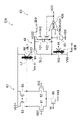
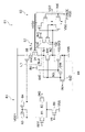
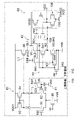
- FIG. 1 is a diagram showing a schematic configuration of a solid-state imaging device according to the present disclosure
- FIG. 3 is a block diagram showing a detailed configuration example of a pixel
- FIG. 3 is a block diagram showing a detailed configuration example of a comparison circuit
- FIG. It is a figure explaining the detailed structure of a pixel circuit.
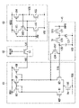
- 2 is a circuit diagram showing an example of the configuration of a comparison circuit according to the first embodiment
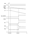
- FIG. 4 is a timing chart showing an example of operation of the comparison circuit according to the first embodiment
- 4 is a circuit diagram showing an example of operation of the comparison circuit according to the first embodiment
- FIG. FIG. 7B is a circuit diagram illustrating an example of the operation of the comparison circuit following FIG. 7A;
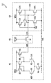
- FIG. 11 is a circuit diagram showing an example of the configuration of a comparison circuit according to a third embodiment
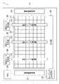
- FIG. It is a conceptual diagram which comprises a solid-state imaging device by laminating
- FIG. 3 is a diagram showing a circuit configuration example in the case of configuring a solid-state imaging device with two semiconductor substrates;
- 1 is a block diagram showing a configuration example of an imaging device as an electronic device according to the present disclosure;
- comparators for brevity, embodiments of comparators, AD converters, solid-state imaging devices, and electronic devices will be described with reference to the drawings.
- the following description focuses on the main components of the comparator, AD converter, solid-state imaging device, and electronic equipment, but the comparator, AD converter, solid-state imaging device, and electronic equipment are not illustrated or described. There can be components and functions. The following description does not exclude components or features not shown or described.
- FIG. 1 shows a schematic configuration of a solid-state imaging device according to the present disclosure.
- the solid-state imaging device 1 of FIG. 1 has a pixel array section 22 in which pixels 21 are arranged in a two-dimensional array on a semiconductor substrate 11 using, for example, silicon (Si) as a semiconductor.
- the pixel array section 22 is also provided with a time code transfer section 23 that transfers the time code generated by the time code generation section 26 to each pixel 21 .
- a pixel drive circuit 24 Around the pixel array section 22 on the semiconductor substrate 11 are a pixel drive circuit 24, a DAC (D/A converter) 25, a time code generation section 26, a vertical drive circuit 27, an output section 28, and a timing generation circuit 29. is formed.
- Each of the pixels 21 arranged in a two-dimensional array is provided with a pixel circuit 41 and an ADC 42, as will be described later with reference to FIG. diode) generates a charge signal corresponding to the amount of light received, converts it to a digital pixel signal SIG, and outputs it.
- the pixel drive circuit 24 drives the pixel circuit 41 (FIG. 2) within the pixel 21 .
- the DAC 25 generates a reference signal (reference voltage signal) REF, which is a slope signal whose level (voltage) monotonously decreases over time, and supplies it to each pixel 21 .
- the time code generation unit 26 generates a time code used when each pixel 21 converts the analog pixel signal SIG into a digital signal (AD conversion), and supplies the time code to the corresponding time code transfer unit 23 .
- a plurality of time code generation units 26 are provided for the pixel array unit 22 , and the pixel array unit 22 includes time code transfer units 23 as many as the time code generation units 26 . . That is, the time code generating section 26 and the time code transfer section 23 for transferring the time code generated therein correspond one-to-one.
- the vertical drive circuit 27 performs control to output the digital pixel signal SIG generated in the pixel 21 to the output section 28 in a predetermined order based on the timing signal supplied from the timing generation circuit 29 .
- a digital pixel signal SIG output from the pixel 21 is output from the output unit 28 to the outside of the solid-state imaging device 1 .
- the output unit 28 performs predetermined digital signal processing such as black level correction processing for correcting the black level and CDS (Correlated Double Sampling) processing as necessary, and then outputs to the outside.
- the timing generation circuit 29 is composed of a timing generator or the like that generates various timing signals, and supplies the generated various timing signals to the pixel drive circuit 24, the DAC 25, the vertical drive circuit 27, and the like.
- the solid-state imaging device 1 is configured as described above. In FIG. 1, all the circuits forming the solid-state imaging device 1 are formed on one semiconductor substrate 11, as described above. It is also possible to adopt a configuration in which the circuits to be connected are divided and arranged on a plurality of semiconductor substrates 11 .
- FIG. 2 is a block diagram showing a detailed configuration example of the pixel 21. As shown in FIG. 2
- the pixel 21 is composed of a pixel circuit 41 and an ADC (AD converter) 42.
- the pixel circuit 41 outputs a charge signal corresponding to the amount of received light to the ADC 42 as an analog pixel signal SIG.
- the ADC 42 converts the analog pixel signal SIG supplied from the pixel circuit 41 into a digital signal.
- the ADC 42 is composed of a comparison circuit 51 (comparator) and a data storage section 52.
- the comparison circuit 51 compares the reference signal REF supplied from the DAC 25 and the pixel signal SIG, and outputs an output signal VCO as a comparison result signal representing the comparison result.
- the comparison circuit 51 inverts the output signal VCO when the reference signal REF and the pixel signal SIG are the same (at the same voltage).
- the comparison circuit 51 is composed of a differential input circuit 61, a voltage conversion circuit 62, and a positive feedback circuit (PFB) 63, the details of which will be described later with reference to FIG.
- PFB positive feedback circuit
- the output signal VCO from the comparison circuit 51 is input to the data storage unit 52, and the WR signal representing the pixel signal write operation and the RD signal representing the pixel signal read operation are supplied from the vertical drive circuit 27 to the data storage unit 52.
- a signal and a WORD signal that controls the readout timing of the pixels 21 during the pixel signal readout operation are supplied from the vertical drive circuit 27 .
- the time code generated by the time code generator 26 is also supplied via the time code transfer section 23 .
- the data storage unit 52 is composed of a latch control circuit 71 that controls the write operation and read operation of the time code based on the WR signal and the RD signal, and a latch storage unit 72 that stores the time code.
- the latch control circuit 71 is supplied from the time code transfer section 23 and updated every unit time while the Hi (High) output signal VCO is being input from the comparison circuit 51.
- the time code is stored in the latch storage section 72 .
- the reference signal REF and the pixel signal SIG become the same voltage and the output signal VCO supplied from the comparison circuit 51 is inverted to Lo (Low)
- the supplied time code is written (updated). Stop, and make the latch storage unit 72 retain the time code last stored in the latch storage unit 72 .
- the time code stored in the latch storage unit 72 represents the time when the pixel signal SIG and the reference signal REF became equal, and data indicating that the pixel signal SIG was the reference voltage at that time, that is, digitization represents the light intensity value.
- the operation of the pixels 21 is changed from write operation to read operation.
- the latch control circuit 71 reads out the time code ( A digital pixel signal SIG) is output to the time code transfer unit 23 .
- the time code transfer unit 23 sequentially transfers the supplied time code in the column direction (vertical direction) and supplies it to the output unit 28 .
- the inverted time code when the output signal VCO read out from the latch storage unit 72 in the time code read operation is inverted.
- the digitized pixel data indicating that the pixel signal SIG was the reference voltage at that time is also called AD conversion pixel data.
- FIG. 3 is a circuit diagram showing detailed configurations of the differential input circuit 61, the voltage conversion circuit 62, and the positive feedback circuit 63 that constitute the comparison circuit 51. As shown in FIG. 3
- the differential input circuit 61 compares the pixel signal SIG output from the pixel circuit 41 in the pixel 21 and the reference signal REF output from the DAC 25, and when the pixel signal SIG is higher than the reference signal REF, a predetermined Outputs a signal (current).
- the differential input circuit 61 includes transistors 81 and 82 forming a differential pair, transistors 83 and 84 forming a current mirror, a transistor 85 as a constant current source that supplies a current IB corresponding to the input bias current Vb, and a differential input circuit 61 . It is composed of a transistor 86 that outputs the output signal HVO of the dynamic input circuit 61 .
- the transistors 81, 82, and 85 are composed of NMOS (Negative Channel MOS) transistors, and the transistors 83, 84, and 86 are composed of PMOS (Positive Channel MOS) transistors.
- the gate of the transistor 81 receives the reference signal REF output from the DAC 25
- the gate of the transistor 82 receives the pixel output from the pixel circuit 41 in the pixel 21 .
- a signal SIG is input.
- the sources of transistors 81 and 82 are connected to the drain of transistor 85, and the source of transistor 85 is connected to a predetermined voltage VSS (VSS ⁇ VDD2 ⁇ VDD1).
- the drain of the transistor 81 is connected to the gates of the transistors 83 and 84 and the drain of the transistor 83 that constitute the current mirror circuit, and the drain of the transistor 82 is connected to the drain of the transistor 84 and the gate of the transistor 86 .
- the sources of transistors 83, 84 and 86 are connected to a first power supply voltage VDD1.
- the voltage conversion circuit 62 is composed of an NMOS transistor 91, for example.
- the drain of transistor 91 is connected to the drain of transistor 86 of differential input circuit 61, the source of transistor 91 is connected to a predetermined connection point in positive feedback circuit 63, and the gate of transistor 86 is connected to bias voltage VBIAS. It is connected.
- the transistors 81 to 86 forming the differential input circuit 61 are circuits that operate at a high voltage up to the first power supply voltage VDD1, and the positive feedback circuit 63 operates at a second power supply voltage VDD2 lower than the first power supply voltage VDD1.
- the voltage conversion circuit 62 converts the output signal HVO input from the differential input circuit 61 into a low-voltage signal (conversion signal) LVI that allows the positive feedback circuit 63 to operate, and supplies the converted signal to the positive feedback circuit 63 .
- the bias voltage VBIAS may be a voltage that does not destroy the transistors 101 to 105 of the positive feedback circuit 63 operating at a constant voltage.
- the positive feedback circuit 63 inverts the output signal HVO from the differential input circuit 61 when the pixel signal SIG is higher than the reference signal REF based on the conversion signal LVI obtained by converting the output signal HVO into a signal corresponding to the second power supply voltage VDD2. output a comparison result signal. Also, the positive feedback circuit 63 speeds up the transition speed when the output signal VCO output as the comparison result signal is inverted.
- the positive feedback circuit 63 is composed of five transistors 101-105.
- the transistors 101, 102, and 104 are composed of PMOS transistors, and the transistors 103 and 105 are composed of NMOS transistors.
- the source of the transistor 91 which is the output terminal of the voltage conversion circuit 62, is connected to the drains of the transistors 102 and 103 and the gates of the transistors 104 and 105.
- the sources of transistors 101 and 104 are connected to the second supply voltage VDD2
- the drain of transistor 101 is connected to the source of transistor 102
- the gate of transistor 102 is connected to transistors 104 and 105 which are also the output of positive feedback circuit 63.
- the sources of transistors 103 and 105 are connected to a predetermined voltage VSS.
- An initialization signal INI is supplied to the gates of the transistors 101 and 103 .
- the transistors 104 and 105 constitute an inverter circuit, and the connection point between their drains is the output terminal from which the comparator circuit 51 outputs the output signal VCO.
- FIG. 4 is a circuit diagram showing the details of the pixel circuit 41 added to the comparison circuit 51 shown in FIG.
- the pixel circuit 41 is composed of a photodiode (PD) 121 as a photoelectric conversion element, an ejection transistor 122, a transfer transistor 123, a reset transistor 124, and an FD (floating diffusion layer) 125.
- PD photodiode
- the discharge transistor 122 is used when adjusting the exposure period. Specifically, when the discharge transistor 122 is turned on when the exposure period is to be started at an arbitrary timing, the charge accumulated in the photodiode 121 is discharged, so the discharge transistor 122 is turned off. After that, the exposure period is started.
- the transfer transistor 123 transfers the charges generated by the photodiode 121 to the FD 125 .
- a reset transistor 124 resets the charge held in the FD 125 .
- FD 125 is connected to the gate of transistor 82 of differential input circuit 61 . Thereby, the transistor 82 of the differential input circuit 61 also functions as an amplification transistor of the pixel circuit 41 .
- the source of the reset transistor 124 is connected to the gate of the transistor 82 of the differential input circuit 61 and the FD 125 , and the drain of the reset transistor 124 is connected to the drain of the transistor 82 . Therefore, there is no fixed reset voltage to reset the charge on FD125. This is because by controlling the circuit state of the differential input circuit 61, the reset voltage for resetting the FD 125 can be arbitrarily set using the reference signal REF.
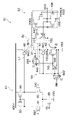
- FIG. 5 is a circuit diagram showing an example of the configuration of the comparison circuit 51 according to the first embodiment.
- the differential input circuit 61 outputs the output signal HVO based on the comparison between the input signal (pixel signal SIG) and the reference signal REF as described above.
- the output signal HVO shown in FIGS. 3 and 4 passes through the output signal line SL1 of the differential input circuit 61 (comparison unit).
- the conversion signal LVI shown in FIGS. 3 and 4 passes through the output signal line SL2 of the voltage conversion circuit 62.
- Both the output signal lines SL1 and SL2 may be included as the output signal lines of the comparator.
- reference voltage node VDD1 is, for example, the reference voltage node VDDH.
- the reference voltage node VDD2 is, for example, the reference voltage node VDDL.
- the reference voltage node VSS is, for example, the ground node GND.
- output signal line SL2 corresponds to output signal line SL1
- reference voltage node VDD2 is at the same voltage level as reference voltage node VDD1.
- the positive feedback circuit 63 has a NOR gate 106 instead of the inverter circuits (transistors 104 and 105) shown in FIGS.
- One of the two input terminals of the NOR gate 106 is connected to the second node N2 of the output signal line SL2, and the drive signal FORCEVCO is input to the other.
- NOR gate 106 outputs the NOR of the input signals to the gate of transistor 102 as a positive feedback signal.
- the positive feedback circuit 63 shown in FIG. 5 operates in substantially the same manner as the positive feedback circuit 63 shown in FIGS.
- the gate of the transistor 101 receives an initialization signal INI2.
- the initialization signal INI2 may be the same as the initialization signal INI, as shown in FIGS.
- the comparison circuit 51 further includes a logic fixing section 64 .
- the logic fixing section 64 is connected between the differential input circuit 61 and the positive feedback circuit 63 . More specifically, logic fixer 64 is connected between voltage conversion circuit 62 and positive feedback circuit 63 .
- the logic fixing unit 64 fixes the logic of the second node N2 of the output signal line SL2 to the first logic until the logic of the output signal HVO of the differential input circuit 61 is inverted.
- the first logic is Lo, for example.
- the logic fixing unit 64 fixes the logic of the second node N2 of the output signal line SL2 so as to fix the voltage level, for example.
- the logic fixer 64 releases the fixation of the logic of the second node N2 of the output signal line SL2 at the timing when the logic of the output signal HVO of the differential input circuit 61 is inverted.
- erroneous logic inversion of the comparison result signal (output signal VCO) of the comparison circuit 51 can be suppressed.
- the logic fixing section 64 has a first transistor 641 , a second transistor 642 , a third transistor 643 , a fourth transistor 644 and a fifth transistor 645 .
- Either one of the second transistor 642 and the third transistor 643 may be the transistor 103 of the positive feedback circuit 63 shown in FIGS. 3 and 4, not included in the logic fixing section 64.
- the third transistor 643 is the transistor 103 not included in the logic fixing section 64 .
- the first transistor 641 is connected between the first node N1 and the second node N2 on the output signal line SL2.
- the first node N1 is arranged on the output signal line SL2 between the differential input circuit 61 and the first transistor 641 .
- the second node N2 is arranged on the output signal line SL2 between the first transistor 641 and the positive feedback circuit 63.
- FIG. A gate of the first transistor 641 is electrically connected to the first node N1.
- the first transistor 641 is, for example, an NMOS transistor.
- the second transistor 642 is connected between the first node N1 and the reference voltage node VSS (second reference voltage node).
- the gate of the second transistor 642 receives an initialization signal INI.
- the second transistor 642 is, for example, an NMOS transistor.
- the third transistor 643 is connected between the second node N2 and the reference voltage node VSS. By keeping the third transistor 643 on until the output signal HVO of the differential input circuit 61 is turned on, the logic of the second node N2 of the output signal line SL2 can be fixed to the first logic. A gate of the third transistor 643 is electrically connected to the third node N3.
- the third transistor 643 is, for example, an NMOS transistor.
- the fourth transistor 644 is connected between the gate (third node N3) of the third transistor 643 and the reference voltage node VSS.
- a gate of the fourth transistor 644 is electrically connected to the first node N1.
- the fourth transistor 644 is, for example, an NMOS transistor.
- the fifth transistor 645 is connected between the gate (third node N3) of the third transistor 643 and the reference voltage node VDD2 (third reference voltage node).
- Reference voltage node VDD2 for example, has a voltage level between reference voltage node VDD1 and reference voltage node VSS.
- An initialization signal XINI is input to the gate of the fifth transistor 645 .
- the initialization signal XINI is a signal with a level opposite to that of the initialization signal INI.
- the fifth transistor 645 is, for example, a PMOS transistor. That is, the fifth transistor 645 is a transistor with a conductivity type different from that of the first transistor 641 , the second transistor 642 , the third transistor 643 and the fourth transistor 644 .
- FIG. 6 is a timing chart showing an example of the operation of the comparison circuit 51 according to the first embodiment.
- FIGS. 7A to 7C are circuit diagrams showing an example of the operation of the comparison circuit 51 according to the first embodiment.
- a circle mark on a transistor indicates an ON state, and an X mark on a transistor indicates an OFF state.
- a solid arrow indicates that a current flows through an on-state transistor.
- a dashed arrow indicates that a leakage current flows through the off-state transistor.
- the reference signal REF is raised in the initial state.
- each node (first node N1, second node N2, and third node N3) of the comparison circuit 51 is reset to an initial state before AD conversion.
- the initialization signal INI transitions from Lo to Hi.
- Initialization signal XINI transitions from Hi to Lo.
- the voltage level of the reference signal REF is higher than the voltage level of the pixel signal SIG.
- FIG. 7A shows a circuit diagram at time t1 in FIG.
- the transistor 86 of the differential input circuit 61 shown in FIG. 7A is off.
- the second transistor 642 since the initialization signal INI (first initialization signal) transitions to Hi, the second transistor 642 is turned on. Accordingly, the first node N1 is electrically connected to the reference voltage node VSS. Therefore, as shown in FIG. 6, the voltage level of the first node N1 drops and the logic of the first node N1 transitions to Lo. As a result, the first transistor 641 and the fourth transistor 644 are turned off.
- the fifth transistor 645 is turned on. Accordingly, the third node N3 is electrically connected to the reference voltage node VDD2 and charged. Therefore, as shown in FIG. 6, the voltage level of the third node N3 rises and the logic of the third node N3 transitions to Hi. This turns on the third transistor 643 . Accordingly, the second node N2 is electrically connected to the reference voltage node VSS. Therefore, as shown in FIG. 6, the voltage level of the second node N2 drops and the logic of the second node N2 transitions to Lo. Also, since the logic of the second node N2 is Lo, the NOR gate 106 turns off the transistor 102 .
- the initialization signal INI transitions from Hi to Lo.
- Initialization signal XINI transitions from Lo to Hi.
- AD conversion is started.
- FIG. 7B shows a circuit diagram from time t2 to time t4 in FIG.
- Time t4 is the time immediately before time t5 at which the logic of the output signal HVO of the differential input circuit 61 is inverted.
- the transistor 86 of the differential input circuit 61 shown in FIG. 7B is off.
- the second transistor 642 since the initialization signal INI is Lo, the second transistor 642 is off. As a result, the first node N1 is electrically disconnected from the reference voltage node VSS. Since the initialization signal XINI is Hi, the fifth transistor 645 is off. This electrically disconnects the third node N3 from the reference voltage node VDD2.
- the other first transistor 641, third transistor 643, fourth transistor 644, and transistor 102 of the positive feedback circuit 63 are off, on, off, and off, respectively, as in FIG. 7A.
- a leak current flows from the reference voltage node VDD1 to the first node N1 of the output signal line SL2.
- a leak current flows from the first node N1 to the reference voltage node VSS using the second transistor 642 in the off state as a leak current path.
- Leakage current flows from the first node N1 to the second node N2 using the first transistor 641 in the off state as a leakage current path.
- Leakage current passing through the off transistor 86 can charge the first node N1 and increase the voltage level of the first node N1.
- the first transistor 641 and the second transistor 642 in the off state function as leakage current paths, and the leakage current passing through the transistor 86 flows to the second node N2 and the reference voltage node VSS, respectively.
- a leak current flows from the reference voltage node VDD2 to the third node N3 using the fifth transistor 645 in the off state as a leak current path.
- a leak current flows from the third node N3 to the reference voltage node VSS using the fourth transistor 644 in the off state as a leak current path.
- a leakage current passing through the off-state fourth transistor 644 may drain the third node N3 and reduce the voltage level of the third node N3.
- a leakage current path from the reference voltage node VDD2 via the fifth transistor 645 in the off state can suppress the voltage level drop at the third node N3. Therefore, as shown in FIG. 6, the logic of the third node N3 can be fixed to Hi. As a result, the ON state of the third transistor 643 can be maintained.
- a leak current flows from the reference voltage node VDD2 to the second node N2 of the output signal line SL2 using the off-state transistor 102 of the positive feedback circuit 63 as a leak current path.
- This leakage current passes through the ON-state third transistor 643 and is dumped to the reference voltage node VSS.
- the logic of the second node N2 can be fixed to Lo.
- a high power supply side leakage current path and a low power supply side leakage current path are arranged at each of the first node N1 and the third node N3.
- the voltage levels at the first node N1 and the third node N3 can be fixed so as not to change due to leakage current.
- the logic fixing unit 64 causes the leakage current flowing from the differential input circuit 61 connected to the reference voltage node VDD1 (first reference voltage node) to the output signal lines SL1 and SL2 to flow to the reference voltage node VSS. Then, the logic of the second node N2 of the output signal line SL2 is fixed to the first logic. As a result, erroneous inversion of the comparison result of the comparison circuit 51 can be suppressed.
- the logic fixing unit 64 reduces the leak current flowing from the differential input circuit 61 to the first node N1 by a plurality of It flows to the second node N2 and the reference voltage node VSS through the leakage current path.
- leakage current flows also in FIG. 7A. However, the leakage current flowing through the off-state transistors 86, 102 and the first transistor 641 passes through the on-state third transistor 643 and flows to the reference voltage node VSS, as in FIG. 7B.
- FIG. 7C shows a circuit diagram at time t5 in FIG.
- the transistor 86 When the voltage level is inverted between the reference signal REF and the pixel signal SIG, the transistor 86 is turned on. Therefore, the logic of the output signal HVO of the differential input circuit 61 is inverted. Accordingly, the first node N1 is charged by the reference voltage node VDD1 and the voltage level of the first node N1 increases. As a result, the logic of the first node N1 transitions to Hi.
- the fourth transistor 644 When the voltage level of the first node N1 reaches the threshold voltage of the fourth transistor 644, the fourth transistor 644 is turned on. As a result, the charge at the third node N3 is discharged to the reference voltage node VSS, and the voltage level at the third node N3 is lowered. As a result, the logic of the third node transitions to Lo. This turns off the third transistor 643 . Therefore, the fixation of the logic of the second node N2 by the third transistor 643 is released.
- the first transistor 641 When the voltage level of the first node N1 reaches the threshold voltage of the first transistor 641, the first transistor 641 is turned on. The current flowing through the on-state transistor 86 does not flow to the second transistor 642 side, but passes through the on-state first transistor 641 and flows to the second node N2. Therefore, the conversion signal LVI of the voltage conversion circuit 62 (the output signal HVO of the differential input circuit 61) is supplied to the second node N2. As described above, since the third transistor 643 is in the off state, fixing of the voltage level and logic of the second node N2 is stopped. Accordingly, the second node N2 is charged and the voltage level of the second node N2 increases. As a result, the logic of the second node N2 transitions to Hi.
- the voltage level of the output signal VCO of the NOR gate 106 falls.
- the transistor 102 is turned on to electrically connect the second node N2 of the output signal line SL2 to the reference voltage node VDD2.
- the positive feedback circuit 63 speeds up the inversion of the output signal VCO.
- the data storage unit 52 stores time data (N-bit DATA[1] to DATA[N]) at the time when the output signal VCO is inverted.
- the operation of the comparison circuit 51 after time t5 is substantially the same as the operation of the comparison circuit 51 when the logic fixing section 64 is not provided, as shown in FIG. 3, for example.
- CDS Correlated Double Sampling processing may be performed. For example, after the reset level P-phase data is acquired, the signal level D-phase data is acquired.
- the logic fixing unit 64 maintains the voltage level until the logic of the output signal HVO of the differential input circuit 61 (conversion signal LVI of the voltage conversion circuit 62) is inverted. , the logic of the second node N2 is fixed to the first logic. That is, the logic fixer 64 prevents the second node N2 from floating. As a result, an increase in the voltage level of the second node N2 due to the leakage current of the transistor 86 can be suppressed. As a result, erroneous inversion of the comparison result signal (output signal VCO) of the comparison circuit 51 due to leakage current can be suppressed. Therefore, malfunction of the comparison circuit 51 can be suppressed.
- the ADC 42 is provided for each pixel 21 . Therefore, the logic fixing portion 64 is also provided for each pixel 21 . Note that the ADC 42 may be provided for each of the multiple pixels 21 .
- FIG. 8 is a circuit diagram showing an example of the configuration of the comparison circuit 51a according to the first comparative example.
- a comparison circuit 51a shown in FIG. 8 is substantially the same as the comparison circuit 51 shown in FIG. 3 without the logic fixing unit 64 provided.
- the transistors 86, 102 and 103 are off before the inversion of the output signal HVO from time t2 to time t4. Therefore, the output signal line SL2 is in a floating state until the output signal HVO of the differential input circuit 61 is inverted at time t5.
- a leak current I leak may flow through the output signal line SL2.
- the leakage current I leak flowing from the reference voltage nodes VDD1 and VDD2 to the output signal line SL2 through the transistors 86 and 102 is larger than the leakage current I leak flowing from the output signal line SL2 to the reference voltage node VSS through the transistor 103. If it is large, the output signal line SL2 will be charged and the voltage level of the output signal line SL2 will rise.
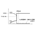
- FIG. 9 is a schematic diagram showing voltage levels of each node of the comparison circuit 51a according to the first comparative example. 9 shows the voltage level of the output signal line SL2 and the output signal VCO of the comparison circuit 51. FIG. The vertical axis indicates voltage level and the horizontal axis indicates time.
- the leakage current I leak causes the voltage level of the output signal line SL2 to rise.
- the voltage level of the output signal VCO decreases from the voltage level of the reference voltage node VDD2.
- the voltage level of the output signal VCO reaches the threshold voltage Vth of the transistor 102 within the D-phase period, positive feedback is applied and erroneous inversion occurs. That is, as shown in FIG. 9, the voltage level of the output signal line SL2 reaches the voltage level of the reference voltage node VDD2 before the D-phase period ends, and the output signal VCO transitions to Lo.
- the voltage level of the output signal line SL2 is substantially constant at the voltage level of the reference voltage node VSS, as indicated by the dashed-dotted line in FIG.
- the output signal VCO is erroneously inverted within the D-phase period, for example, blown-out highlights will occur in the captured image.
- the second node N2 of the output signal line SL2 is not in a floating state, but fixed to the voltage level of the reference voltage node VSS by the third transistor 643. .
- the leak current I_leak flowing through the output signal line SL2 through the transistors 86 and 102 can be properly discharged to the reference voltage node VSS.
- an increase in the voltage level of the second node N2 due to the leakage current I leak can be suppressed, and erroneous inversion of the comparison result signal (output signal VCO) of the comparison circuit 51 can be suppressed.
- FIG. 10 is a circuit diagram showing an example of the configuration of the comparison circuit 51b according to the second comparative example.
- an increase in the voltage level of the output signal line SL2 is suppressed by adjusting the threshold voltage of the transistor.
- the leakage current I leak of the off-state transistor is expressed by Equation 1 using the gate-source voltage Vgs and the threshold voltage Vth. Therefore, the leakage current I leak is proportional to the threshold voltage.
- the leakage current I leak flowing out of the output signal line SL2 can be relatively increased with respect to the leakage current I leak flowing into the output signal line SL2.
- the threshold voltage of the transistor 102 it is possible to reduce the leakage current I leak that flows from the reference voltage node VDD2 to the output signal line SL2 using the transistor 102 as a leakage current path.
- the leakage current I_leak flowing from the output signal line SL2 to the reference voltage node VSS via the transistor 103 can be increased.
- FIG. 11 is a schematic diagram showing voltage levels of each node of the comparison circuit 51b according to the second comparative example. 11 shows the voltage level of the signal line L2 and the output signal VCO of the comparison circuit 51. FIG. 11 indicate voltage levels of the output signal line SL2 and the output signal VCO according to the first comparative example shown in FIG.
- the rate of increase in the voltage level of the output signal line SL2 can be reduced. That is, it is possible to lengthen the time required for charging the output signal line SL2 and suppress erroneous inversion of the output signal VCO until the end of the AD period.
- the threshold voltage of transistor 103 is the next highest, and the threshold voltage of transistor 91 is the lowest. That is, four types of transistors with adjusted threshold voltages are used in the voltage conversion circuit 62 and the positive feedback circuit 63 .
- the capacitor 65 is, for example, a MOS (Metal Oxide Semiconductor) capacitor.
- MOS Metal Oxide Semiconductor
- the rise in the voltage level of the second node N2 of the output signal line SL2 is suppressed by the circuit configuration without changing the threshold voltages of the transistor 102 and the third transistor 643 (transistor 103). can do.
- the types of transistors other than the transistor 91 of the voltage conversion circuit 62 can be unified.
- the threshold voltages of the transistor 86 (sixth transistor) of the differential input circuit 61, the transistor of the logic fixing section 64, and the transistor of the positive feedback circuit 63 are substantially the same. As a result, it is possible to suppress degradation of circuit stability due to variations in threshold voltage. Also, it is possible to suppress a decrease in the degree of freedom in design.
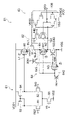
- FIG. 12 is a circuit diagram showing an example of the configuration of the comparison circuit 51 according to the second embodiment.
- the second embodiment differs from the first embodiment in the method of inputting the initialization signal XINI to the gate of the fifth transistor 645 .
- the logic fixing unit 64 further includes an inverter INV.
- the inverter INV is connected between the gate of the second transistor 642 and the gate of the fifth transistor 645 .
- the inverter INV generates an inverted pulse of the initialization signal INI. Therefore, a signal obtained by inverting the initialization signal INI is input to the gate of the fifth transistor 645 instead of the initialization signal XINI.
- wiring is increased due to the addition of the initialization signal XINI compared to the first and second comparative examples. If the number of wires drawn from the outside of the pixel array section 22 increases, the width of other wires such as the initialization signal INI and the drive signal FORCEVCO may become narrow.
- the inverter INV can be arranged in the empty space of the capacitor 65, which is a MOS capacitor, and an increase in required space can be suppressed.
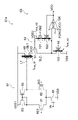
- FIG. 13 is a circuit diagram showing an example of the configuration of the comparison circuit 51 according to the third embodiment.
- the third embodiment differs from the first embodiment in that the conductivity type of the fifth transistor 645 is reversed.
- the fifth transistor 645 is not a PMOS transistor but an NMOS transistor. Therefore, the first transistor 641, the second transistor 642, the third transistor 643, the fourth transistor 644 and the fifth transistor 645 are all NMOS transistors of the same conductivity type.
- the same signal as the initialization signal INI input to the gate of the second transistor 642 is input to the gate of the fifth transistor 645 .
- the fourth embodiment differs from the first embodiment in the threshold voltage of the transistor 86 shown in FIG.
- the threshold voltage of transistor 86 (sixth transistor) is lower than a predetermined value.
- the threshold voltage of the transistor 86 is, for example, lower than the threshold voltage of the transistors included in the positive feedback circuit 63 and logic fixing section 64 .
- the second node N2 of the signal line L2 is connected to the reference voltage node VSS by the logic fixer 64, and the logic is fixed. Therefore, even if the leakage current of transistor 86 increases, the leakage current is dumped to the reference voltage node VSS. Since erroneous inversion of the comparison result signal of the comparison circuit 51 due to leakage current is suppressed, the threshold voltage of the transistor 86 can be lowered to suppress an increase in inversion delay.
- the solid-state imaging device 1 is formed on one semiconductor substrate 11.
- the solid-state imaging device 1 is configured by separately forming circuits on a plurality of semiconductor substrates 11. may
- FIG. 14 shows a conceptual diagram of the solid-state imaging device 1 configured by stacking two semiconductor substrates 11, an upper substrate 11A and a lower substrate 11C.
- At least a pixel circuit 41 including a photodiode 121 is formed on the upper substrate 11A.
- At least a data storage section 52 for storing a time code and a time code transfer section 23 are formed on the lower substrate 11C.
- the upper substrate 11A and the lower substrate 11C are joined by, for example, metal bonding such as Cu—Cu.
- FIG. 15 shows a circuit configuration example formed on each of the upper substrate 11A and the lower substrate 11C.
- the pixel circuit 41 and the circuits of the transistors 81, 82, and 85 of the differential input circuit 61 of the ADC 42 are formed on the upper substrate 11A.
- FIG. 15 shows part of the pixel circuit 41 .
- a circuit of the ADC 42 excluding the transistors 81, 82, and 85 and the time code transfer section 23 are formed on the lower substrate 11C. Therefore, the logic fixing portion 64 is arranged on the lower substrate 11C. Note that the data storage unit 52 and the time code transfer unit 23 are omitted in FIG.
- the present disclosure is not limited to application to solid-state imaging devices. That is, the present disclosure is applicable to an image capture unit (photoelectric conversion unit) such as an imaging device such as a digital still camera or a video camera, a mobile terminal device having an imaging function, or a copying machine using a solid-state imaging device as an image reading unit. It is applicable to general electronic equipment using a solid-state imaging device.
- the solid-state imaging device may be formed as a single chip, or may be a module having an imaging function in which an imaging unit and a signal processing unit or an optical system are packaged together.
- FIG. 16 is a block diagram showing a configuration example of an imaging device as an electronic device according to the present disclosure.
- An imaging device 800 in FIG. 16 includes an optical unit 801 including a lens group, a solid-state imaging device (imaging device) 802 adopting the configuration of the solid-state imaging device 1 in FIG. Processor) circuit 803 .
- the imaging device 800 also includes a frame memory 804 , a display unit 805 , a recording unit 806 , an operation unit 807 and a power supply unit 808 .
- DSP circuit 803 , frame memory 804 , display unit 805 , recording unit 806 , operation unit 807 and power supply unit 808 are interconnected via bus line 809 .
- the optical unit 801 captures incident light (image light) from a subject and forms an image on the imaging surface of the solid-state imaging device 802 .
- the solid-state imaging device 802 converts the amount of incident light imaged on the imaging surface by the optical unit 801 into an electric signal on a pixel-by-pixel basis, and outputs the electric signal as a pixel signal.
- the solid-state imaging device 802 the solid-state imaging device 1 of FIG. It is possible to use a solid-state imaging device having a time code transfer section 23 that can reduce the time to .
- the display unit 805 is composed of a panel-type display device such as a liquid crystal panel or an organic EL (Electro Luminescence) panel, for example, and displays moving images or still images captured by the solid-state imaging device 802 .
- a recording unit 806 records a moving image or still image captured by the solid-state imaging device 802 in a recording medium such as a hard disk or a semiconductor memory.
- the operation unit 807 issues operation commands for various functions of the imaging device 800 under the user's operation.
- a power source unit 808 appropriately supplies various power sources as operating power sources for the DSP circuit 803, the frame memory 804, the display unit 805, the recording unit 806, and the operation unit 807 to these supply targets.
- the solid-state imaging device 1 adopting any of the configurations described above as the solid-state imaging device 802
- power consumption can be reduced while speeding up the determination speed of AD conversion. Therefore, even in the imaging device 800 such as a video camera, a digital still camera, and a camera module for a mobile device such as a mobile phone, high-speed imaging and low power consumption can be realized.
- comparison circuit 51 and the ADC 42 are described as parts incorporated in the solid-state imaging device 1, but each can be a separately distributed product (comparator, AD converter).
- present disclosure is applicable not only to solid-state imaging devices but also to semiconductor devices in general having other semiconductor integrated circuits.
- circuit configuration of each of the embodiments described above has been described as a circuit configuration in which electrons are used as charges, the present disclosure can also be configured as a circuit configuration in which holes are used as charges. Further, in each circuit configuration described above, a circuit configuration in which the polarities of the transistors (NMOS transistor and PMOS transistor) are exchanged can also be realized. In that case, the control signal input to the transistor is a signal with opposite Hi and Low.
- the reference signal REF is a slope signal whose level (voltage) monotonically decreases over time. It can also be an increasing slope signal.
- this technique can take the following structures. (1) a comparator that outputs an output signal based on a comparison between the input signal and the reference signal; Logic for fixing the logic of the output signal line of the comparing unit to the first logic until the logic of the output signal is inverted, and releasing the fixation of the logic of the output signal line at the timing when the logic of the output signal is inverted. a fixed part; A comparator. (2) The logic fixing section changes the logic of the output signal line so that leakage current flowing from the comparing section connected to the first reference voltage node to the output signal line flows to the second reference voltage node. The comparator of claim 1, locking to said first logic based on a second reference voltage node.
- the logic fixer fixes the leak current flowing from the comparator to the first node on the output signal line through a plurality of leak current paths to the second node on the output signal line and the second reference voltage node.
- the logic of the second node is set to the first logic based on the second reference voltage node so that leakage current flowing from the first node to the second node flows to the second reference voltage node.
- the comparator of (2) fixed to .
- the logic fixing unit a first transistor connected between a first node and a second node on the output signal line and having a gate electrically connected to the first node; at least one of a second transistor connected between the first node and a second reference voltage node, and a third transistor connected between the second node and the second reference voltage node; a fourth transistor connected between the gate of the third transistor and the second reference voltage node and having a gate electrically connected to the first node; a fifth transistor connected between the gate of the third transistor and a third reference voltage node; has (1) to (3) fixing the logic of the second node to the first logic based on the second reference voltage node by turning on the third transistor until the logic of the output signal is inverted; A comparator according to any one of .
- the logic fixing unit By initializing the voltage level of the first node based on the second reference voltage node based on the first initialization signal input to the gate of the second transistor, the first transistor and the fourth transistor off and The third transistor is turned on by initializing the voltage level of the gate of the third transistor based on the third reference voltage node based on the second initialization signal input to the gate of the fifth transistor. and making the logic of the second node the first logic based on the second reference voltage node.
- the logic fixing unit causing a leakage current flowing from the comparison unit to the first node to flow to the second node and the second reference voltage node through the first transistor and the second transistor in an off state, respectively;
- the second node is arranged so that the leakage current flowing from the first node to the second node through the first transistor in the off state flows to the second reference voltage node through the third transistor in the on state. to the first logic based on the second reference voltage node.
- the logic fixing unit reduces leakage current flowing from the third reference voltage node to the gate of the third transistor through the fifth transistor in the off state to the gate of the third transistor through the fourth transistor in the off state.
- the comparator of (6) that feeds the second reference voltage node.
- the logic fixing unit By turning on the fourth transistor at the timing when the logic of the output signal output to the first node is inverted, the third transistor is turned off to release the fixation of the logic of the second node; any one of (4) to (7), wherein the output signal is supplied to the second node by turning on the first transistor at the timing when the logic of the output signal output to the first node is inverted;
- a comparator according to claim 1. the first transistor, the second transistor, the third transistor and the fourth transistor are transistors of the same conductivity type;
- the fifth transistor according to any one of (4) to (8), wherein the fifth transistor has a conductivity type different from that of the first transistor, the second transistor, the third transistor, and the fourth transistor. Comparator.
- the first transistor, the second transistor, the third transistor, the fourth transistor, and the fifth transistor are transistors of the same conductivity type;
- the comparator according to any one of (4) to (8), wherein the gate of the fifth transistor receives the same signal as the signal input to the gate of the second transistor.
- the comparison unit has a sixth transistor connected between a first reference voltage node of the comparison unit and the output signal line;
- the comparison unit has a sixth transistor connected between a first reference voltage node of the comparison unit and the output signal line;
- the comparator according to any one of (1) to (11), wherein the threshold voltage of the sixth transistor is lower than the threshold voltage of the transistor included in the logic fixing section.
- (14) further comprising a positive feedback circuit for speeding up the transition speed when the logic of the comparison result signal of the comparator is inverted based on the output signal;
- the logic fixing unit changes the logic of the output signal line to the second reference voltage node so that leakage current flowing from the positive feedback circuit connected to the fourth reference voltage node to the output signal line flows to the second reference voltage node.
- a comparator according to any one of (1) to (13), which locks to said first logic based on a reference voltage node.
- a voltage conversion circuit that converts the output signal of the comparison unit operating at the voltage of the first reference voltage node higher than the voltage of the fourth reference voltage node into a signal corresponding to the voltage of the fourth reference voltage node.
- An AD converter comprising: (17) a comparator that outputs an output signal based on a comparison between the input signal and the reference signal; Logic for fixing the logic of the output signal line of the comparison unit to the first logic until the logic of the output signal is inverted, and fixing the logic of the output signal line at the timing when the logic of the output signal is inverted.
- a comparator comprising a data storage unit for storing a time code when the comparison result signal of the comparator is inverted
- an AD converter comprising a pixel circuit that outputs, as the input signal, a charge signal generated by photoelectrically converting light incident on a pixel to the comparison unit
- a solid-state imaging device (18) a first chip on which the pixel circuit is arranged; The solid-state imaging device according to (17), further comprising: a second chip stacked with the first chip and on which the logic fixing section is arranged. (19) The solid-state imaging device according to (17) or (18), wherein the AD converter is arranged for each pixel.
- a comparison unit that outputs an output signal based on a comparison between the input signal and the reference signal; Logic for fixing the logic of the output signal line of the comparison unit to the first logic until the logic of the output signal is inverted, and fixing the logic of the output signal line at the timing when the logic of the output signal is inverted.
- a comparator comprising a data storage unit for storing a time code when the comparison result signal of the comparator is inverted;
- an AD converter comprising a pixel circuit that outputs, as the input signal, a charge signal generated by photoelectrically converting light incident on a pixel to the comparison unit;
- An electronic device comprising a solid-state imaging device.
- 1 solid-state imaging device 11A upper substrate, 11C lower substrate, 21 pixel, 41 pixel circuit, 42 ADC, 51 comparison circuit, 52 data storage unit, 61 differential input circuit, 62 voltage conversion circuit, 63 positive feedback circuit, 64 Logic fixing part, 641 first transistor, 642 second transistor, 643 third transistor, 644 fourth transistor, 645 fifth transistor, INV inverter, SL2 output signal line, N1 first node, N2 second node, N3 third node
Landscapes
- Engineering & Computer Science (AREA)
- Multimedia (AREA)
- Signal Processing (AREA)
- Physics & Mathematics (AREA)
- Nonlinear Science (AREA)
- Transforming Light Signals Into Electric Signals (AREA)
- Manipulation Of Pulses (AREA)
- Analogue/Digital Conversion (AREA)
Abstract
[課題]比較結果の誤反転を抑制する。 [解決手段]比較器は、入力信号と参照信号との比較に基づいた出力信号を出力する比較部と、前記出力信号の論理が反転するまで、前記比較部の出力信号線の論理を第1論理に固定し、前記出力信号の論理が反転するタイミングで、前記出力信号線の論理の固定を解除する論理固定部と、を備える。
Description
本開示による実施形態は、比較器、AD変換器、固体撮像装置及び電子機器に関する。
固体撮像装置の信号読み出し側に、ADC(Analog to Digital Converter)が設けられる。ADC用の比較器に、画素信号と参照信号とを比較する差動入力回路と、この差動入力回路による出力信号に正帰還をかけて、比較器による比較結果の信号の遷移時間を高速化する正帰還回路と、が搭載される場合がある(特許文献1、2参照)。
しかしながら、差動入力回路と正帰還回路との間のノードは、差動入力回路の出力信号が反転するまでの間、フローティング状態になる。オフ状態のトランジスタを介して電源からのリーク電流がフローティング状態のノードに流れると、ノードの電圧レベルが上昇する可能性がある。この場合、AD変換期間の終了までに、正帰還がかかることにより比較結果が誤反転してしまう問題があった。
そこで、本開示では、比較結果の誤反転を抑制することができる比較器、AD変換器、固体撮像装置及び電子機器を提供するものである。
上記の課題を解決するために、本開示によれば、
入力信号と参照信号との比較に基づいた出力信号を出力する比較部と、
前記出力信号の論理が反転するまで、前記比較部の出力信号線の論理を第1論理に固定し、前記出力信号の論理が反転するタイミングで、前記出力信号線の論理の固定を解除する論理固定部と、
を備える、比較器が提供される。
入力信号と参照信号との比較に基づいた出力信号を出力する比較部と、
前記出力信号の論理が反転するまで、前記比較部の出力信号線の論理を第1論理に固定し、前記出力信号の論理が反転するタイミングで、前記出力信号線の論理の固定を解除する論理固定部と、
を備える、比較器が提供される。
前記論理固定部は、第1基準電圧ノードと接続される前記比較部から前記出力信号線に流れるリーク電流を、第2基準電圧ノードに流すように、前記出力信号線の論理を前記第2基準電圧ノードに基づいた前記第1論理に固定してもよい。
前記論理固定部は、前記比較部から前記出力信号線上の第1ノードに流れるリーク電流を、複数のリーク電流パスを介して前記出力信号線上の第2ノード及び前記第2基準電圧ノードに流すことにより、前記第1ノードから前記第2ノードに流れるリーク電流を前記第2基準電圧ノードに流すように、前記第2ノードの論理を前記第2基準電圧ノードに基づいた前記第1論理に固定してもよい。
前記論理固定部は、
前記出力信号線上の第1ノードと第2ノードとの間に接続され、ゲートが前記第1ノードと電気的に接続される第1トランジスタと、
前記第1ノードと第2基準電圧ノードとの間に接続される第2トランジスタ、及び、前記第2ノードと前記第2基準電圧ノードとの間に接続される第3トランジスタの少なくとも一方と、
前記第3トランジスタのゲートと、前記第2基準電圧ノードと、の間に接続され、ゲートが前記第1ノードと電気的に接続される第4トランジスタと、
前記第3トランジスタのゲートと、第3基準電圧ノードと、の間に接続される第5トランジスタと、
を有し、
前記出力信号の論理が反転するまで前記第3トランジスタをオンすることにより、前記第2ノードの論理を前記第2基準電圧ノードに基づいた前記第1論理に固定してもよい。
前記出力信号線上の第1ノードと第2ノードとの間に接続され、ゲートが前記第1ノードと電気的に接続される第1トランジスタと、
前記第1ノードと第2基準電圧ノードとの間に接続される第2トランジスタ、及び、前記第2ノードと前記第2基準電圧ノードとの間に接続される第3トランジスタの少なくとも一方と、
前記第3トランジスタのゲートと、前記第2基準電圧ノードと、の間に接続され、ゲートが前記第1ノードと電気的に接続される第4トランジスタと、
前記第3トランジスタのゲートと、第3基準電圧ノードと、の間に接続される第5トランジスタと、
を有し、
前記出力信号の論理が反転するまで前記第3トランジスタをオンすることにより、前記第2ノードの論理を前記第2基準電圧ノードに基づいた前記第1論理に固定してもよい。
前記論理固定部は、
前記第2トランジスタのゲートに入力される第1初期化信号に基づいて前記第1ノードの電圧レベルを前記第2基準電圧ノードに基づいて初期化することにより、前記第1トランジスタ及び前記第4トランジスタをオフし、
前記第5トランジスタのゲートに入力される第2初期化信号に基づいて前記第3トランジスタのゲートの電圧レベルを前記第3基準電圧ノードに基づいて初期化することにより、前記第3トランジスタをオンするとともに、前記第2ノードの論理を前記第2基準電圧ノードに基づいた前記第1論理にしてもよい。
前記第2トランジスタのゲートに入力される第1初期化信号に基づいて前記第1ノードの電圧レベルを前記第2基準電圧ノードに基づいて初期化することにより、前記第1トランジスタ及び前記第4トランジスタをオフし、
前記第5トランジスタのゲートに入力される第2初期化信号に基づいて前記第3トランジスタのゲートの電圧レベルを前記第3基準電圧ノードに基づいて初期化することにより、前記第3トランジスタをオンするとともに、前記第2ノードの論理を前記第2基準電圧ノードに基づいた前記第1論理にしてもよい。
前記論理固定部は、
前記比較部から前記第1ノードに流れるリーク電流を、オフ状態の前記第1トランジスタ及び前記第2トランジスタを介して、それぞれ前記第2ノード及び前記第2基準電圧ノードに流し、
オフ状態の前記第1トランジスタを介して前記第1ノードから前記第2ノードに流れるリーク電流を、オン状態の前記第3トランジスタを介して前記第2基準電圧ノードに流すように、前記第2ノードの論理を前記第2基準電圧ノードに基づいた前記第1論理に固定してもよい。
前記比較部から前記第1ノードに流れるリーク電流を、オフ状態の前記第1トランジスタ及び前記第2トランジスタを介して、それぞれ前記第2ノード及び前記第2基準電圧ノードに流し、
オフ状態の前記第1トランジスタを介して前記第1ノードから前記第2ノードに流れるリーク電流を、オン状態の前記第3トランジスタを介して前記第2基準電圧ノードに流すように、前記第2ノードの論理を前記第2基準電圧ノードに基づいた前記第1論理に固定してもよい。
前記論理固定部は、オフ状態の前記第5トランジスタを介して前記第3基準電圧ノードから前記第3トランジスタのゲートに流れるリーク電流を、オフ状態の前記第4トランジスタを介して、前記第2基準電圧ノードに流してもよい。
前記論理固定部は、
前記第1ノードに出力される前記出力信号の論理が反転するタイミングで前記第4トランジスタをオンすることにより、前記第3トランジスタをオフして前記第2ノードの論理の固定を解除し、
前記第1ノードに出力される前記出力信号の論理が反転するタイミングで前記第1トランジスタをオンすることにより、前記出力信号を前記第2ノードに供給してもよい。
前記第1ノードに出力される前記出力信号の論理が反転するタイミングで前記第4トランジスタをオンすることにより、前記第3トランジスタをオフして前記第2ノードの論理の固定を解除し、
前記第1ノードに出力される前記出力信号の論理が反転するタイミングで前記第1トランジスタをオンすることにより、前記出力信号を前記第2ノードに供給してもよい。
前記第1トランジスタ、前記第2トランジスタ、前記第3トランジスタ及び前記第4トランジスタは、同じ導電型のトランジスタであり、
前記第5トランジスタは、前記第1トランジスタ、前記第2トランジスタ、前記第3トランジスタ及び前記第4トランジスタとは異なる導電型のトランジスタであってもよい。
前記第5トランジスタは、前記第1トランジスタ、前記第2トランジスタ、前記第3トランジスタ及び前記第4トランジスタとは異なる導電型のトランジスタであってもよい。
前記第2トランジスタのゲートと、前記第5トランジスタのゲートと、の間に接続されるインバータをさらに備えてもよい。
前記第1トランジスタ、前記第2トランジスタ、前記第3トランジスタ、前記第4トランジスタ及び前記第5トランジスタは、同じ導電型のトランジスタであり、
前記第5トランジスタのゲートは、前記第2トランジスタのゲートに入力される信号と同じ信号が入力されてもよい。
前記第5トランジスタのゲートは、前記第2トランジスタのゲートに入力される信号と同じ信号が入力されてもよい。
前記比較部は、前記比較部の第1基準電圧ノードと、前記出力信号線と、の間に接続される第6トランジスタを有し、
前記第6トランジスタの閾値電圧は、前記論理固定部が有するトランジスタの閾値電圧と略同じであってもよい。
前記第6トランジスタの閾値電圧は、前記論理固定部が有するトランジスタの閾値電圧と略同じであってもよい。
前記比較部は、前記比較部の第1基準電圧ノードと、前記出力信号線と、の間に接続される第6トランジスタを有し、
前記第6トランジスタの閾値電圧は、前記論理固定部が有するトランジスタの閾値電圧よりも低くてもよい。
前記第6トランジスタの閾値電圧は、前記論理固定部が有するトランジスタの閾値電圧よりも低くてもよい。
前記出力信号に基づいて、前記比較器の比較結果信号の論理が反転するときの遷移速度を高速化する正帰還回路をさらに備え、
前記論理固定部は、第4基準電圧ノードと接続される前記正帰還回路から前記出力信号線に流れるリーク電流を、第2基準電圧ノードに流すように、前記出力信号線の論理を前記第2基準電圧ノードに基づいた前記第1論理に固定してもよい。
前記論理固定部は、第4基準電圧ノードと接続される前記正帰還回路から前記出力信号線に流れるリーク電流を、第2基準電圧ノードに流すように、前記出力信号線の論理を前記第2基準電圧ノードに基づいた前記第1論理に固定してもよい。
前記第4基準電圧ノードよりも高い第1基準電圧ノードの電圧で動作する前記比較部の前記出力信号を、前記第4基準電圧ノードの電圧に対応する信号に変換する電圧変換回路をさらに備えてもよい。
本開示によれば、入力信号と参照信号との比較に基づいた出力信号を出力する比較部と、
前記出力信号の論理が反転するまで、前記比較部の出力信号線の論理を第1論理に固定し、前記出力信号の論理が反転するタイミングで、前記出力信号線の論理の固定を回路する論理固定部と、
を備える比較器と、
前記比較器の比較結果信号が反転したときの時刻コードを記憶するデータ記憶部と、
を備える、AD変換器が提供される。
前記出力信号の論理が反転するまで、前記比較部の出力信号線の論理を第1論理に固定し、前記出力信号の論理が反転するタイミングで、前記出力信号線の論理の固定を回路する論理固定部と、
を備える比較器と、
前記比較器の比較結果信号が反転したときの時刻コードを記憶するデータ記憶部と、
を備える、AD変換器が提供される。
本開示によれば、入力信号と参照信号との比較に基づいた出力信号を出力する比較部と、
前記出力信号の論理が反転するまで、前記比較部の出力信号線の論理を第1論理に固定し、前記出力信号の論理が反転するタイミングで、前記出力信号線の論理の固定を回路する論理固定部と、
を備える比較器と、
前記比較器の比較結果信号が反転したときの時刻コードを記憶するデータ記憶部と、
を備えるAD変換器と、
画素に入射された光を受光して光電変換することで生成された電荷信号を、前記入力信号として前記比較部に出力する画素回路と、
を備える、固体撮像装置が提供される。
前記出力信号の論理が反転するまで、前記比較部の出力信号線の論理を第1論理に固定し、前記出力信号の論理が反転するタイミングで、前記出力信号線の論理の固定を回路する論理固定部と、
を備える比較器と、
前記比較器の比較結果信号が反転したときの時刻コードを記憶するデータ記憶部と、
を備えるAD変換器と、
画素に入射された光を受光して光電変換することで生成された電荷信号を、前記入力信号として前記比較部に出力する画素回路と、
を備える、固体撮像装置が提供される。
前記画素回路が配置される第1チップと、
前記第1チップと積層され、前記論理固定部が配置される第2チップと、をさらに備えてもよい。
前記第1チップと積層され、前記論理固定部が配置される第2チップと、をさらに備えてもよい。
前記AD変換器は、画素ごとに配置されてもよい。
本開示によれば、入力信号と参照信号との比較に基づいた出力信号を出力する比較部と、
前記出力信号の論理が反転するまで、前記比較部の出力信号線の論理を第1論理に固定し、前記出力信号の論理が反転するタイミングで、前記出力信号線の論理の固定を回路する論理固定部と、
を備える比較器と、
前記比較器の比較結果信号が反転したときの時刻コードを記憶するデータ記憶部と、
を備えるAD変換器と、
画素に入射された光を受光して光電変換することで生成された電荷信号を、前記入力信号として前記比較部に出力する画素回路と、
を備える固体撮像装置
を備える、電子機器が提供される。
前記出力信号の論理が反転するまで、前記比較部の出力信号線の論理を第1論理に固定し、前記出力信号の論理が反転するタイミングで、前記出力信号線の論理の固定を回路する論理固定部と、
を備える比較器と、
前記比較器の比較結果信号が反転したときの時刻コードを記憶するデータ記憶部と、
を備えるAD変換器と、
画素に入射された光を受光して光電変換することで生成された電荷信号を、前記入力信号として前記比較部に出力する画素回路と、
を備える固体撮像装置
を備える、電子機器が提供される。
以下、図面を参照して、比較器、AD変換器、固体撮像装置及び電子機器の実施形態について説明する。以下では、比較器、AD変換器、固体撮像装置及び電子機器の主要な構成部分を中心に説明するが、比較器、AD変換器、固体撮像装置及び電子機器には、図示又は説明されていない構成部分や機能が存在しうる。以下の説明は、図示又は説明されていない構成部分や機能を除外するものではない。
<固体撮像装置の概略構成例>
図1は、本開示に係る固体撮像装置の概略構成を示している。
図1は、本開示に係る固体撮像装置の概略構成を示している。
図1の固体撮像装置1は、半導体として例えばシリコン(Si)を用いた半導体基板11に、画素21が2次元アレイ状に配列された画素アレイ部22を有する。画素アレイ部22には、時刻コード発生部26で生成された時刻コードを各画素21に転送する時刻コード転送部23も設けられている。そして、半導体基板11上の画素アレイ部22の周辺には、画素駆動回路24、DAC(D/A Converter)25、時刻コード発生部26、垂直駆動回路27、出力部28、及びタイミング生成回路29が形成されている。
2次元アレイ状に配列された画素21のそれぞれには、図2を参照して後述するように、画素回路41とADC42が設けられており、画素21は、画素内の受光素子(例えば、フォトダイオード)で受光した光量に応じた電荷信号を生成し、デジタルの画素信号SIGに変換して出力する。
画素駆動回路24は、画素21内の画素回路41(図2)を駆動する。DAC25は、時間経過に応じてレベル(電圧)が単調減少するスロープ信号である参照信号(基準電圧信号)REFを生成し、各画素21に供給する。時刻コード発生部26は、各画素21が、アナログの画素信号SIGをデジタルの信号に変換(AD変換)する際に使用される時刻コードを生成し、対応する時刻コード転送部23に供給する。時刻コード発生部26は、画素アレイ部22に対して複数個設けられており、画素アレイ部22内には、時刻コード発生部26に対応する数だけ、時刻コード転送部23が設けられている。即ち、時刻コード発生部26と、そこで生成された時刻コードを転送する時刻コード転送部23は、1対1に対応する。
垂直駆動回路27は、画素21内で生成されたデジタルの画素信号SIGを、タイミング生成回路29から供給されるタイミング信号に基づいて、所定の順番で出力部28に出力させる制御を行う。画素21から出力されたデジタルの画素信号SIGは、出力部28から固体撮像装置1の外部へ出力される。出力部28は、黒レベルを補正する黒レベル補正処理やCDS(Correlated Double Sampling;相関2重サンプリング)処理など、所定のデジタル信号処理を必要に応じて行い、その後、外部へ出力する。
タイミング生成回路29は、各種のタイミング信号を生成するタイミングジェネレータなどによって構成され、生成した各種のタイミング信号を、画素駆動回路24、DAC25、垂直駆動回路27等に供給する。
固体撮像装置1は、以上のように構成されている。なお、図1では、上述したように、固体撮像装置1を構成する全ての回路が、1つの半導体基板11上に形成されるように説明したが、後述するように、固体撮像装置1を構成する回路を複数枚の半導体基板11に分けて配置する構成とすることもできる。
<画素の詳細構成例>
図2は、画素21の詳細構成例を示すブロック図である。
図2は、画素21の詳細構成例を示すブロック図である。
画素21は、画素回路41とADC(AD変換器)42で構成されている。
画素回路41は、受光した光量に応じた電荷信号をアナログの画素信号SIGとしてADC42に出力する。ADC42は、画素回路41から供給されたアナログの画素信号SIGをデジタル信号に変換する。
ADC42は、比較回路51(比較器)とデータ記憶部52で構成される。
比較回路51は、DAC25から供給される参照信号REFと画素信号SIGを比較し、比較結果を表す比較結果信号として、出力信号VCOを出力する。比較回路51は、参照信号REFと画素信号SIGが同一(の電圧)になったとき、出力信号VCOを反転させる。
比較回路51は、差動入力回路61、電圧変換回路62、及び正帰還回路(PFB:positive feedback)63により構成されるが、詳細は図3を参照して後述する。
データ記憶部52には、比較回路51から出力信号VCOが入力される他、垂直駆動回路27から、画素信号の書き込み動作であることを表すWR信号、画素信号の読み出し動作であることを表すRD信号、及び、画素信号の読み出し動作中における画素21の読み出しタイミングを制御するWORD信号が、垂直駆動回路27から供給される。また、時刻コード転送部23を介して、時刻コード発生部26で生成された時刻コードも供給される。
データ記憶部52は、WR信号及びRD信号に基づいて、時刻コードの書き込み動作と読み出し動作を制御するラッチ制御回路71と、時刻コードを記憶するラッチ記憶部72で構成される。
ラッチ制御回路71は、時刻コードの書き込み動作においては、比較回路51からHi(High)の出力信号VCOが入力されている間、時刻コード転送部23から供給される、単位時間ごとに更新される時刻コードをラッチ記憶部72に記憶させる。そして、参照信号REFと画素信号SIGが同一(の電圧)になり、比較回路51から供給される出力信号VCOがLo(Low)に反転されたとき、供給される時刻コードの書き込み(更新)を中止し、最後にラッチ記憶部72に記憶された時刻コードをラッチ記憶部72に保持させる。ラッチ記憶部72に記憶された時刻コードは、画素信号SIGと参照信号REFが等しくなった時刻を表しており、画素信号SIGがその時刻の基準電圧であったことを示すデータ、即ち、デジタル化された光量値を表す。
参照信号REFの掃引が終了し、画素アレイ部22内の全ての画素21のラッチ記憶部72に時刻コードが記憶された後、画素21の動作が、書き込み動作から読み出し動作に変更される。
ラッチ制御回路71は、時刻コードの読み出し動作においては、読み出しタイミングを制御するWORD信号に基づいて、画素21が自分の読み出しタイミングとなったときに、ラッチ記憶部72に記憶されている時刻コード(デジタルの画素信号SIG)を、時刻コード転送部23に出力する。時刻コード転送部23は、供給された時刻コードを、列方向(垂直方向)に順次転送し、出力部28に供給する。
以下では、時刻コードの書き込み動作においてラッチ記憶部72に書き込まれる時刻コードと区別するため、時刻コードの読み出し動作においてラッチ記憶部72から読み出される出力信号VCOが反転したときの反転時刻コードである、画素信号SIGがその時刻の基準電圧であったことを示すデジタル化された画素データを、AD変換画素データとも称する。
<比較回路の構成例>
図3は、比較回路51を構成する差動入力回路61、電圧変換回路62、及び正帰還回路63の詳細構成を示す回路図である。
図3は、比較回路51を構成する差動入力回路61、電圧変換回路62、及び正帰還回路63の詳細構成を示す回路図である。
差動入力回路61は、画素21内の画素回路41から出力された画素信号SIGと、DAC25から出力された参照信号REFとを比較し、画素信号SIGが参照信号REFよりも高いときに所定の信号(電流)を出力する。
差動入力回路61は、差動対となるトランジスタ81及び82、カレントミラーを構成するトランジスタ83及び84、入力バイアス電流Vbに応じた電流IBを供給する定電流源としてのトランジスタ85、並びに、差動入力回路61の出力信号HVOを出力するトランジスタ86により構成されている。
トランジスタ81、82、及び85は、NMOS(Negative Channel MOS)トランジスタで構成され、トランジスタ83、84、及び86は、PMOS(Positive Channel MOS)トランジスタで構成される。
差動対となるトランジスタ81及び82のうち、トランジスタ81のゲートには、DAC25から出力された参照信号REFが入力され、トランジスタ82のゲートには、画素21内の画素回路41から出力された画素信号SIGが入力される。トランジスタ81と82のソースは、トランジスタ85のドレインと接続され、トランジスタ85のソースは、所定の電圧VSS(VSS<VDD2<VDD1)に接続されている。
トランジスタ81のドレインは、カレントミラー回路を構成するトランジスタ83及び84のゲート及びトランジスタ83のドレインと接続され、トランジスタ82のドレインは、トランジスタ84のドレイン及びトランジスタ86のゲートと接続されている。トランジスタ83、84、及び86のソースは、第1電源電圧VDD1に接続されている。
電圧変換回路62は、例えば、NMOS型のトランジスタ91で構成される。トランジスタ91のドレインは、差動入力回路61のトランジスタ86のドレインと接続され、トランジスタ91のソースは、正帰還回路63内の所定の接続点に接続され、トランジスタ86のゲートは、バイアス電圧VBIASに接続されている。
差動入力回路61を構成するトランジスタ81乃至86は、第1電源電圧VDD1までの高電圧で動作する回路であり、正帰還回路63は、第1電源電圧VDD1よりも低い第2電源電圧VDD2で動作する回路である。電圧変換回路62は、差動入力回路61から入力される出力信号HVOを、正帰還回路63が動作可能な低電圧の信号(変換信号)LVIに変換して、正帰還回路63に供給する。
バイアス電圧VBIASは、定電圧で動作する正帰還回路63の各トランジスタ101乃至105を破壊しない電圧に変換する電圧であれば良い。例えば、バイアス電圧VBIASは、正帰還回路63の第2電源電圧VDD2と同じ電圧(VBIAS=VDD2)とすることができる。
正帰還回路63は、差動入力回路61からの出力信号HVOが第2電源電圧VDD2に対応する信号に変換された変換信号LVIに基づいて、画素信号SIGが参照信号REFよりも高いときに反転する比較結果信号を出力する。また、正帰還回路63は、比較結果信号として出力する出力信号VCOが反転するときの遷移速度を高速化する。
正帰還回路63は、5つのトランジスタ101乃至105で構成される。ここで、トランジスタ101、102、及び104は、PMOSトランジスタで構成され、トランジスタ103及び105は、NMOSトランジスタで構成される。
電圧変換回路62の出力端であるトランジスタ91のソースは、トランジスタ102及び103のドレインと、トランジスタ104及び105のゲートに接続されている。トランジスタ101及び104のソースは、第2電源電圧VDD2に接続され、トランジスタ101のドレインは、トランジスタ102のソースと接続され、トランジスタ102のゲートは、正帰還回路63の出力端でもあるトランジスタ104及び105のドレインと接続されている。トランジスタ103及び105のソースは、所定の電圧VSSに接続されている。トランジスタ101と103のゲートには、初期化信号INIが供給される。
トランジスタ104と105はインバータ回路を構成し、それらのドレインどうしの接続点は、比較回路51が出力信号VCOを出力する出力端となっている。
<画素回路の詳細構成例>
図4を参照して、画素回路41の詳細構成について説明する。
図4を参照して、画素回路41の詳細構成について説明する。
図4は、図3に示した比較回路51に、画素回路41の詳細を追加して示した回路図である。
画素回路41は、光電変換素子としてのフォトダイオード(PD)121、排出トランジスタ122、転送トランジスタ123、リセットトランジスタ124、及び、FD(浮遊拡散層)125で構成されている。
排出トランジスタ122は、露光期間を調整する場合に使用される。具体的には、露光期間を任意のタイミングで開始したいときに排出トランジスタ122をオンさせると、それまでの間にフォトダイオード121に蓄積されていた電荷が排出されるので、排出トランジスタ122がオフされた以降から、露光期間が開始されることになる。
転送トランジスタ123は、フォトダイオード121で生成された電荷をFD125に転送する。リセットトランジスタ124は、FD125に保持されている電荷をリセットする。FD125は、差動入力回路61のトランジスタ82のゲートに接続されている。これにより、差動入力回路61のトランジスタ82は、画素回路41の増幅トランジスタとしても機能する。
リセットトランジスタ124のソースは、差動入力回路61のトランジスタ82のゲート、及び、FD125に接続されており、リセットトランジスタ124のドレインは、トランジスタ82のドレインと接続されている。従って、FD125の電荷をリセットするための固定のリセット電圧がない。これは、差動入力回路61の回路状態を制御することで、FD125をリセットするリセット電圧を、参照信号REFを用いて任意に設定可能であるためである。
<第1実施形態>
[比較回路の構成]
図5は、第1実施形態による比較回路51の構成の一例を示す回路図である。
[比較回路の構成]
図5は、第1実施形態による比較回路51の構成の一例を示す回路図である。
差動入力回路61は、上記のように、入力信号(画素信号SIG)と参照信号REFとの比較に基づいた出力信号HVOを出力する。また、差動入力回路61(比較部)の出力信号線SL1は、図3及び図4に示す出力信号HVOが通過する。電圧変換回路62の出力信号線SL2は、図3及び図4に示す変換信号LVIが通過する。比較部の出力信号線として、出力信号線SL1、SL2の両方が含まれてもよい。
なお、基準電圧ノードVDD1は、例えば、基準電圧ノードVDDHである。基準電圧ノードVDD2は、例えば、基準電圧ノードVDDLである。基準電圧ノードVSSは、例えば、グランドノードGNDである。
以下では、電圧変換回路62が設けられる場合について説明する。しかし、電圧変換回路62が設けられなくてもよい。この場合、出力信号線SL2は出力信号線SL1に対応し、基準電圧ノードVDD2は基準電圧ノードVDD1と同じ電圧レベルである。
正帰還回路63は、図3及び図4に示すインバータ回路(トランジスタ104、105)に代えて、NORゲート106を有する。NORゲート106の2つの入力端子のうち一方は、出力信号線SL2の第2ノードN2に接続され、他方には、駆動信号FORCEVCOが入力される。NORゲート106は、入力信号の否定論理和を正帰還信号としてトランジスタ102のゲートに出力する。図5に示す正帰還回路63は、図3及び図4に示す正帰還回路63とほぼ同様に動作する。また、トランジスタ101のゲートは、初期化信号INI2が入力される。初期化信号INI2は、図3及び図4に示すように、初期化信号INIと同じでよい。
比較回路51は、論理固定部64をさらに備える。
論理固定部64は、差動入力回路61と正帰還回路63との間に接続される。より詳細には、論理固定部64は、電圧変換回路62と正帰還回路63との間に接続される。論理固定部64は、差動入力回路61の出力信号HVOの論理が反転するまで、出力信号線SL2の第2ノードN2の論理を第1論理に固定する。第1論理は、例えば、Loである。論理固定部64は、例えば、電圧レベルを固定させるように、出力信号線SL2の第2ノードN2の論理を固定する。また、論理固定部64は、差動入力回路61の出力信号HVOの論理が反転するタイミングで、出力信号線SL2の第2ノードN2の論理の固定を解除する。これにより、図7Bを参照して後で説明するように、比較回路51の比較結果信号(出力信号VCO)の論理の誤反転を抑制することができる。
論理固定部64は、第1トランジスタ641と、第2トランジスタ642と、第3トランジスタ643と、第4トランジスタ644と、第5トランジスタ645と、を有する。
なお、第2トランジスタ642及び第3トランジスタ643のいずれか一方は、論理固定部64に含まれず、図3及び図4に示す正帰還回路63のトランジスタ103であってもよい。以下では、図5に示すように、第3トランジスタ643が論理固定部64に含まれないトランジスタ103であるとして説明する。
第1トランジスタ641は、出力信号線SL2上の第1ノードN1と第2ノードN2との間に接続される。第1ノードN1は、差動入力回路61と第1トランジスタ641との間の出力信号線SL2上に配置される。第2ノードN2は、第1トランジスタ641と正帰還回路63との間の出力信号線SL2上に配置される。第1トランジスタ641のゲートは、第1ノードN1と電気的に接続される。第1トランジスタ641は、例えば、NMOSトランジスタである。
第2トランジスタ642は、第1ノードN1と、基準電圧ノードVSS(第2基準電圧ノード)と、の間に接続される。第2トランジスタ642のゲートは、初期化信号INIが入力される。第2トランジスタ642は、例えば、NMOSトランジスタである。
第3トランジスタ643は、第2ノードN2と基準電圧ノードVSSとの間に接続される。差動入力回路61の出力信号HVOがオンするまで、第3トランジスタ643がオン状態になることにより、出力信号線SL2の第2ノードN2の論理を第1論理に固定することができる。第3トランジスタ643のゲートは、第3ノードN3と電気的に接続される。第3トランジスタ643は、例えば、NMOSトランジスタである。
第4トランジスタ644は、第3トランジスタ643のゲート(第3ノードN3)と、基準電圧ノードVSSと、の間に接続される。第4トランジスタ644のゲートは、第1ノードN1と電気的に接続される。第4トランジスタ644は、例えば、NMOSトランジスタである。
第5トランジスタ645は、第3トランジスタ643のゲート(第3ノードN3)と、基準電圧ノードVDD2(第3基準電圧ノード)と、の間に接続される。基準電圧ノードVDD2は、例えば、基準電圧ノードVDD1と基準電圧ノードVSSとの間の電圧レベルを有する。第5トランジスタ645のゲートは、初期化信号XINIが入力される。初期化信号XINIは、初期化信号INIとは反対のレベルの信号である。第5トランジスタ645は、例えば、PMOSトランジスタである。すなわち、第5トランジスタ645は、第1トランジスタ641、第2トランジスタ642、第3トランジスタ643及び第4トランジスタ644とは異なる導電型のトランジスタである。
[比較回路の動作]
図6は、第1実施形態による比較回路51の動作の一例を示すタイミングチャートである。
図6は、第1実施形態による比較回路51の動作の一例を示すタイミングチャートである。
図7A~図7Cは、第1実施形態による比較回路51の動作の一例を示す回路図である。トランジスタ上の丸印は、オン状態を示し、トランジスタ上のX印は、オフ状態を示す。実線の矢印は、オン状態のトランジスタに電流が流れることを示す。破線の矢印は、オフ状態のトランジスタにリーク電流が流れることを示す。
図6に示す例では、初期状態において、参照信号REFは持ち上げられている。
まず、時刻t1において、AD変換前に比較回路51の各ノード(第1ノードN1、第2ノードN2及び第3ノードN3)が初期状態にリセットされる。初期化信号INIは、LoからHiに遷移する。初期化信号XINIは、HiからLoに遷移する。また、参照信号REFの電圧レベルは、画素信号SIGの電圧レベルよりも高い。
図7Aは、図6の時刻t1における回路図を示す。
参照信号REFの電圧レベルが画素信号SIGの電圧レベルよりも高いため、図7Aに示す差動入力回路61のトランジスタ86はオフ状態である。
また、初期化信号INI(第1初期化信号)がHiに遷移するため、第2トランジスタ642がオンする。これにより、第1ノードN1は、基準電圧ノードVSSと電気的に接続される。従って、図6に示すように、第1ノードN1の電圧レベルは低下して、第1ノードN1の論理はLoに遷移する。これにより、第1トランジスタ641及び第4トランジスタ644はオフする。
また、初期化信号XINI(第2初期化信号)がLoに遷移するため、第5トランジスタ645はオンする。これにより、第3ノードN3は、基準電圧ノードVDD2と電気的に接続されて充電される。従って、図6に示すように、第3ノードN3の電圧レベルは上昇して、第3ノードN3の論理はHiに遷移する。これにより、第3トランジスタ643はオンする。これにより、第2ノードN2は、基準電圧ノードVSSに電気的に接続される。従って、図6に示すように、第2ノードN2の電圧レベルは低下して、第2ノードN2の論理はLoに遷移する。また、第2ノードN2の論理がLoであるため、NORゲート106により、トランジスタ102はオフする。
次に、時刻t2において、初期化信号INIは、HiからLoに遷移する。初期化信号XINIは、LoからHiに遷移する。時刻t2の後、AD変換が開始される。
次に、時刻t3において、参照信号REFの掃引が開始される。差動入力回路61のトランジスタ86のゲートに接続される信号線L1の電圧レベルは、時間とともに徐々に低下する。
図7Bは、図6の時刻t2から時刻t4までの回路図を示す。時刻t4は、差動入力回路61の出力信号HVOの論理が反転するタイミングである時刻t5の直前の時刻である。
参照信号REFの電圧レベルが画素信号SIGの電圧レベルよりも高いため、図7Bに示す差動入力回路61のトランジスタ86はオフ状態である。
また、初期化信号INIがLoであるため、第2トランジスタ642がオフ状態である。これにより、第1ノードN1は基準電圧ノードVSSから電気的に切り離される。初期化信号XINIがHiであるため、第5トランジスタ645はオフ状態である。これにより、第3ノードN3は基準電圧ノードVDD2から電気的に切り離される。他の第1トランジスタ641、第3トランジスタ643、第4トランジスタ644及び正帰還回路63のトランジスタ102は、図7Aと同様に、それぞれオフ状態、オン状態、オフ状態、オフ状態である。
ここで、トランジスタがオフ状態であっても、ソースとドレインとの間を流れるリーク電流が存在し得る。
トランジスタ86をリーク電流パスとして、基準電圧ノードVDD1から出力信号線SL2の第1ノードN1にリーク電流が流れる。
オフ状態の第2トランジスタ642をリーク電流パスとして、第1ノードN1から基準電圧ノードVSSにリーク電流が流れる。オフ状態の第1トランジスタ641をリーク電流パスとして、第1ノードN1から第2ノードN2にリーク電流が流れる。オフ状態のトランジスタ86を通過するリーク電流により、第1ノードN1が充電されて第1ノードN1の電圧レベルが上昇する可能性がある。しかし、オフ状態の第1トランジスタ641及び第2トランジスタ642がリーク電流パスとして機能し、トランジスタ86を通過するリーク電流は、それぞれ第2ノードN2及び基準電圧ノードVSSに流れる。第1トランジスタ641をリーク電流パスとして第1ノードN1から第2ノードN2に流れるリーク電流は、オン状態の第3トランジスタ643により基準電圧ノードVSSに流れる。これにより、第1ノードN1の電圧レベルの上昇を抑制することができる。従って、図6に示すように、第1ノードN1の論理をLoに固定(維持)することができる。
オフ状態の第5トランジスタ645をリーク電流パスとして、基準電圧ノードVDD2から第3ノードN3にリーク電流が流れる。オフ状態の第4トランジスタ644をリーク電流パスとして、第3ノードN3から基準電圧ノードVSSにリーク電流が流れる。オフ状態の第4トランジスタ644を通過するリーク電流により、第3ノードN3の電荷が抜けて第3ノードN3の電圧レベルが低下する可能性がある。しかし、オフ状態の第5トランジスタ645を介した基準電圧ノードVDD2からのリーク電流パスにより、第3ノードN3の電圧レベルの低下を抑制することができる。従って、図6に示すように、第3ノードN3の論理をHiに固定することができる。この結果、第3トランジスタ643のオン状態を維持することができる。
また、第1ノードN1には、基準電圧ノードVSSへの2つのリーク電流パスである第1トランジスタ641及び第2トランジスタ642が接続されている。もし、第1ノードN1の電圧レベルが上昇すると、第4トランジスタ644のリーク電流が増大して、第3ノードN3の電荷が抜けてしまう。従って、第1ノードN1から基準電圧ノードVSSへのリーク電流パスの数は、多いほどより好ましい。
正帰還回路63のオフ状態のトランジスタ102をリーク電流パスとして、基準電圧ノードVDD2から出力信号線SL2の第2ノードN2にリーク電流が流れる。このリーク電流は、オン状態の第3トランジスタ643を通過して基準電圧ノードVSSへ捨てられる。これにより、第2ノードN2の電圧レベルの上昇を抑制することができる。従って、図6に示すように、第2ノードN2の論理をLoに固定することができる。
また、第1ノードN1及び第3ノードN3のそれぞれに、高電源側のリーク電流パスと低電源側のリーク電流パスとが配置されている。これにより、第1ノードN1及び第3ノードN3における電圧レベルがリーク電流によって変化しないように、固定することができる。この結果、第3トランジスタ643をオン状態で維持しやすくなり、第2ノードN2の論理をより固定しやすくすることができる。
このように、論理固定部64は、基準電圧ノードVDD1(第1基準電圧ノード)と接続される差動入力回路61から出力信号線SL1、SL2に流れるリーク電流を、基準電圧ノードVSSに流すように、出力信号線SL2の第2ノードN2の論理を第1論理に固定する。この結果、比較回路51の比較結果の誤反転を抑制することができる。また、上記のように、第3ノードN3から基準電圧ノードVSSに電荷が抜けることを抑制するため、論理固定部64は、差動入力回路61から第1ノードN1に流れるリーク電流を、複数のリーク電流パスを介して、第2ノードN2及び基準電圧ノードVSSに流す。
なお、図7Aにおいても、リーク電流は流れる。しかし、オフ状態のトランジスタ86、102、第1トランジスタ641を流れるリーク電流は、図7Bと同様に、オン状態の第3トランジスタ643を通過して、基準電圧ノードVSSへ流れる。
次に、時刻t4から時刻t5にかけて、差動入力回路61の出力信号HVOの論理が反転する。
図7Cは、図6の時刻t5の回路図を示す。
参照信号REFと画素信号SIGとの間で電圧レベルが反転すると、トランジスタ86がオンする。従って、差動入力回路61の出力信号HVOの論理が反転する。これにより、第1ノードN1が基準電圧ノードVDD1によって充電され、第1ノードN1の電圧レベルが上昇する。この結果、第1ノードN1の論理がHiに遷移する。
第1ノードN1の電圧レベルが第4トランジスタ644の閾値電圧に達すると、第4トランジスタ644はオンする。これにより、第3ノードN3の電荷が基準電圧ノードVSSへ捨てられ、第3ノードN3の電圧レベルが低下する。この結果、第3ノードの論理がLoに遷移する。これにより、第3トランジスタ643がオフする。従って、第3トランジスタ643による第2ノードN2の論理の固定が解除される。
第1ノードN1の電圧レベルが第1トランジスタ641の閾値電圧に達すると、第1トランジスタ641はオンする。オン状態のトランジスタ86を流れる電流は、第2トランジスタ642側には流れず、オン状態の第1トランジスタ641を通過して第2ノードN2に流れる。従って、電圧変換回路62の変換信号LVI(差動入力回路61の出力信号HVO)が第2ノードN2に供給される。なお、上記のように、第3トランジスタ643はオフ状態であるため、第2ノードN2の電圧レベル及び論理の固定は停止されている。従って、第2ノードN2が充電されて、第2ノードN2の電圧レベルが上昇する。この結果、第2ノードN2の論理がHiに遷移する。
時刻t5において、第2ノードN2の電圧レベルが上昇すると、NORゲート106の出力信号VCOの電圧レベルが低下する。出力信号VCOの電圧レベルが低下すると、トランジスタ102がオンすることにより出力信号線SL2の第2ノードN2は基準電圧ノードVDD2と電気的に接続される。これにより、正帰還回路63によって出力信号VCOの反転が高速化される。また、データ記憶部52では、出力信号VCOが反転した時点の時刻データ(NビットのDATA[1]乃至DATA[N])が記憶される。
時刻t5よりも後の比較回路51の動作は、例えば、図3のような、論理固定部64が設けられない場合の比較回路51の動作とほぼ同様である。
時刻t5の後、読み出しタイミングを制御するWORD信号がHiとなり、Nビットのラッチ信号Col[n](n=1乃至N)(不図示)が、データ記憶部52のラッチ制御回路71から出力される。
なお、CDS(Correlated Double Sampling;相関2重サンプリング)処理が行われてもよい。例えば、リセットレベルのP相データが取得された後、信号レベルのD相データが取得される。
以上のように、第1実施形態によれば、論理固定部64は、差動入力回路61の出力信号HVO(電圧変換回路62の変換信号LVI)の論理が反転するまで、電圧レベルを維持するように、第2ノードN2の論理を第1論理に固定する。すなわち、論理固定部64は、第2ノードN2をフローティング状態にしないようにする。これにより、トランジスタ86のリーク電流による第2ノードN2の電圧レベルの上昇を抑制することができる。この結果、リーク電流による、比較回路51の比較結果信号(出力信号VCO)の誤反転を抑制することができる。従って、比較回路51の誤動作を抑制することができる。
また、ADC42は、画素21ごとに設けられる。したがって、論理固定部64も、画素21ごとに設けられる。なお、ADC42は、複数の画素21ごとに設けられてもよい。
<第1比較例>
図8は、第1比較例による比較回路51aの構成の一例を示す回路図である。図8に示す比較回路51aは、論理固定部64が設けられておらず、図3に示す比較回路51とほぼ同じである。
図8は、第1比較例による比較回路51aの構成の一例を示す回路図である。図8に示す比較回路51aは、論理固定部64が設けられておらず、図3に示す比較回路51とほぼ同じである。
図8に示す例では、時刻t2から時刻t4までの出力信号HVOの反転前において、トランジスタ86、102、103はオフ状態である。従って、出力信号線SL2は、時刻t5において差動入力回路61の出力信号HVOが反転するまで、フローティング状態である。出力信号線SL2には、リーク電流Ileakが流れ得る。例えば、トランジスタ86、102を介して基準電圧ノードVDD1、VDD2から出力信号線SL2に流れるリーク電流Ileakが、トランジスタ103を介して出力信号線SL2から基準電圧ノードVSSに流れるリーク電流Ileakよりも大きい場合、出力信号線SL2が充電されて、出力信号線SL2の電圧レベルが上昇してしまう。
図9は、第1比較例による比較回路51aの各ノードの電圧レベルを示す概略図である。図9は、出力信号線SL2の電圧レベル及び比較回路51の出力信号VCOを示す。縦軸は電圧レベルを示し、横軸は時間を示す。
図9に示すように、差動入力回路61の出力信号HVOの論理が反転する前に、リーク電流Ileakによって出力信号線SL2の電圧レベルが上昇してしまう。出力信号線SL2の電圧レベルの上昇により、出力信号VCOの電圧レベルが基準電圧ノードVDD2の電圧レベルから低下する。D相期間内で出力信号VCOの電圧レベルがトランジスタ102の閾値電圧Vthに達すると、正帰還がかかり誤反転が生じてしまう。すなわち、図9に示すように、D相期間が終わる前に、出力信号線SL2の電圧レベルが基準電圧ノードVDD2の電圧レベルになり、出力信号VCOがLoに遷移してしまう。
出力信号線SL2の電圧レベルは、図9の一点鎖線に示すように、基準電圧ノードVSSの電圧レベルで略一定であることが好ましい。しかし、上記のように、D相期間内で出力信号VCOに誤反転がすると、例えば、撮像画像に白飛びが生じてしまう。
これに対して、第1実施形態では、図7Bに示すように、出力信号線SL2の第2ノードN2はフローティング状態ではなく、第3トランジスタ643によって基準電圧ノードVSSの電圧レベルに固定されている。これにより、トランジスタ86、102を介して出力信号線SL2に流れるリーク電流Ileakを、基準電圧ノードVSSに適切に捨てることができる。この結果、リーク電流Ileakによる第2ノードN2の電圧レベルの上昇を抑制することができ、比較回路51の比較結果信号(出力信号VCO)の誤反転を抑制することができる。
<第2比較例>
図10は、第2比較例による比較回路51bの構成の一例を示す回路図である。第2比較例では、トランジスタの閾値電圧を調整することにより、出力信号線SL2の電圧レベルの上昇が抑制される。
図10は、第2比較例による比較回路51bの構成の一例を示す回路図である。第2比較例では、トランジスタの閾値電圧を調整することにより、出力信号線SL2の電圧レベルの上昇が抑制される。
オフ状態のトランジスタのリーク電流Ileakは、ゲートソース間電圧Vgs及び閾値電圧Vthを用いて、式1により表される。従って、リーク電流Ileakは、閾値電圧に比例する。

閾値電圧を調整することにより、出力信号線SL2に流れ込むリーク電流Ileakに対して、出力信号線SL2からに流れ出るリーク電流Ileakを相対的に増加することができる。例えば、トランジスタ102の閾値電圧を高くすることにより、トランジスタ102をリーク電流パスとして基準電圧ノードVDD2から出力信号線SL2に流れるリーク電流Ileakを低減することができる。また、トランジスタ103の閾値電圧を低くすることにより、トランジスタ103を介して出力信号線SL2から基準電圧ノードVSSに流れるリーク電流Ileakを増大させることができる。
図11は、第2比較例による比較回路51bの各ノードの電圧レベルを示す概略図である。図11は、信号線L2の電圧レベル及び比較回路51の出力信号VCOを示す。なお、図11に示す破線は、図9に示す第1比較例による出力信号線SL2及び出力信号VCOの電圧レベルを示す。
図11に示すように、トランジスタ102、103の閾値電圧の調整により、出力信号線SL2の電圧レベルの上昇速度を低減することができる。すなわち、出力信号線SL2の充電にかかる時間を長くして、AD期間終了までの出力信号VCOの誤反転を抑制することができる。
第2比較例では、図10に示す電圧変換回路62及び正帰還回路63内で、例えば、カスコード接続されたトランジスタ101、102の閾値電圧が最も高く、NORゲート106のトランジスタの閾値電圧が次に高く、トランジスタ103の閾値電圧が次に高く、トランジスタ91の閾値電圧が最も低い。すなわち、電圧変換回路62及び正帰還回路63内で、閾値電圧を調整した4種類のトランジスタが用いられる。
しかし、複数の種類のトランジスタが用いられる場合、閾値電圧のばらつきの影響が大きく回路の安定性が劣化してしまう。また、次のタイプの回路の再設計時の検討項目が増加してしまう。すなわち、設計自由度が低下してしまう。
さらに、トランジスタごとに製造工程が必要になり、開発費が増加してしまう。また、トランジスタ103の閾値電圧を低くすることに伴うランダムノイズの影響が大きくなってしまう。この場合、例えば、フィルタとして機能するキャパシタ65を追加する必要がある。キャパシタ65は、例えば、MOS(Metal Oxide Semiconductor)キャパシタである。また、プロセス依存、すなわち、プロセス技術によるばらつきが大きく、汎用性及び設計自由度が低下してしまう。
これに対して、第1実施形態では、トランジスタ102及び第3トランジスタ643(トランジスタ103)の閾値電圧を変更することなく、回路構成により出力信号線SL2の第2ノードN2の電圧レベルの上昇を抑制することができる。これにより、電圧変換回路62のトランジスタ91以外のトランジスタの種類を統一することができる。例えば、差動入力回路61のトランジスタ86(第6トランジスタ)、論理固定部64が有するトランジスタ、及び、正帰還回路63が有するトランジスタの閾値電圧は、略同じである。この結果、閾値電圧のばらつきによる回路の安定性の劣化を抑制することができる。また、設計自由度の低下を抑制することができる。
さらに、トランジスタごとの製造工程を共通化して開発費の増加を抑制することができる。また、トランジスタの閾値電圧を低下させる調整を行わないため、ランダムノイズの影響が大きくなることを抑制することができる。また、ノイズ低減用のキャパシタ65が不要になり、低回路面積化及びチャージ電流を低減することができる。なお、第1実施形態では、第2比較例と比較して4つのトランジスタ(第1トランジスタ641、第2トランジスタ642、第4トランジスタ644及び第5トランジスタ645)が追加されている。しかし、キャパシタ65の空きスペースに、追加された4つのトランジスタを配置することができる。また、汎用性及び設計自由度の低下を抑制することができる。
<第2実施形態>
図12は、第2実施形態による比較回路51の構成の一例を示す回路図である。第2実施形態は、第1実施形態と比較して、第5トランジスタ645のゲートへの初期化信号XINIの入力方法が異なっている。
図12は、第2実施形態による比較回路51の構成の一例を示す回路図である。第2実施形態は、第1実施形態と比較して、第5トランジスタ645のゲートへの初期化信号XINIの入力方法が異なっている。
論理固定部64は、インバータINVをさらに備える。
インバータINVは、第2トランジスタ642のゲートと、第5トランジスタ645のゲートと、の間に接続される。インバータINVは、初期化信号INIの反転のパルスを生成する。従って、初期化信号INIが反転された信号が、初期化信号XINIに代えて、第5トランジスタ645のゲートに入力される。
第1実施形態では、第1比較例及び第2比較例と比較して、初期化信号XINIの追加によって配線が増加してしまう。画素アレイ部22の外から引いてくる配線数が増えると、例えば、初期化信号INI及び駆動信号FORCEVCO等の他の配線の配線幅が狭くなってしまう可能性がある。
これに対して、第2実施形態では、インバータINVを設けることにより配線数の増加を抑制することができる。また、第2比較例と比較して、例えば、MOSキャパシタであるキャパシタ65の空きスペースにインバータINVを配置することができ、必要なスペースの増大を抑制することができる。
<第3実施形態>
図13は、第3実施形態による比較回路51の構成の一例を示す回路図である。第3実施形態は、第5トランジスタ645の導電型が逆になっている点で、第1実施形態とは異なっている。
図13は、第3実施形態による比較回路51の構成の一例を示す回路図である。第3実施形態は、第5トランジスタ645の導電型が逆になっている点で、第1実施形態とは異なっている。
図13に示す例では、第5トランジスタ645は、PMOSトランジスタではなく、NMOSトランジスタである。従って、第1トランジスタ641、第2トランジスタ642、第3トランジスタ643、第4トランジスタ644及び第5トランジスタ645は、全て同じ導電型の、NMOSトランジスタである。
また、第5トランジスタ645のゲートには、第2トランジスタ642のゲートに入力される初期化信号INIと同じ信号が入力される。これにより、初期化信号XINIの入力が不要になり、第2実施形態と同様に、配線数の増加を抑制することができる。
<第4実施形態>
第4実施形態は、第1実施形態と比較して、図5に示すトランジスタ86の閾値電圧が異なる。トランジスタ86(第6トランジスタ)の閾値電圧は、所定値よりも低い。トランジスタ86の閾値電圧は、例えば、正帰還回路63及び論理固定部64が有するトランジスタの閾値電圧よりも低い。
第4実施形態は、第1実施形態と比較して、図5に示すトランジスタ86の閾値電圧が異なる。トランジスタ86(第6トランジスタ)の閾値電圧は、所定値よりも低い。トランジスタ86の閾値電圧は、例えば、正帰還回路63及び論理固定部64が有するトランジスタの閾値電圧よりも低い。
論理固定部64を追加することにより、図8を参照して説明した第1比較例と比較して、反転遅延が増大してしまう可能性がある。そこで、トランジスタ86の駆動力を上げることにより、反転遅延の増大を抑制することができる。
第1比較例では、トランジスタ86の駆動力を上げるために閾値電圧を下げると、トランジスタ86のリーク電流が増大する。従って、比較回路51aの出力信号VCOの誤反転が生じやすくなってしまう。
これに対して、第4実施形態では、図7Bを参照して説明したように、論理固定部64によって信号線L2の第2ノードN2は基準電圧ノードVSSと接続され、論理が固定される。従って、トランジスタ86のリーク電流が増大しても、リーク電流は基準電圧ノードVSSに捨てられる。リーク電流による比較回路51の比較結果信号の誤反転が抑制されているため、トランジスタ86の閾値電圧を下げて、反転遅延の増大を抑制することができる。
<複数基板構成>
これまでの説明では、固体撮像装置1が、1枚の半導体基板11上に形成されるものとして説明したが、複数枚の半導体基板11に回路を作り分けることで、固体撮像装置1を構成してもよい。
これまでの説明では、固体撮像装置1が、1枚の半導体基板11上に形成されるものとして説明したが、複数枚の半導体基板11に回路を作り分けることで、固体撮像装置1を構成してもよい。
図14は、上側基板11Aと下側基板11Cの2枚の半導体基板11を積層することで固体撮像装置1を構成する概念図を示している。
上側基板11Aには、フォトダイオード121を含む画素回路41が少なくとも形成されている。下側基板11Cには、時刻コードを記憶するデータ記憶部52と時刻コード転送部23が少なくとも形成されている。上側基板11Aと下側基板11Cは、例えば、Cu-Cuなどの金属結合などにより接合される。
図15は、上側基板11Aと下側基板11Cのそれぞれに形成される回路構成例を示している。
上側基板11Aには、画素回路41と、ADC42のうちの差動入力回路61のトランジスタ81、82、及び85の回路が形成されている。なお、図15では、画素回路41の一部が示されている。下側基板11Cには、トランジスタ81、82、及び85を除くADC42の回路と時刻コード転送部23が形成されている。従って、論理固定部64は、下側基板11Cに配置される。なお、図15では、データ記憶部52及び時刻コード転送部23は省略されている。
<電子機器への適用例>
本開示は、固体撮像装置への適用に限られるものではない。即ち、本開示は、デジタルスチルカメラやビデオカメラ等の撮像装置や、撮像機能を有する携帯端末装置や、画像読取部に固体撮像装置を用いる複写機など、画像取込部(光電変換部)に固体撮像装置を用いる電子機器全般に対して適用可能である。固体撮像装置は、ワンチップとして形成された形態であってもよいし、撮像部と信号処理部または光学系とがまとめてパッケージングされた撮像機能を有するモジュール状の形態であってもよい。
本開示は、固体撮像装置への適用に限られるものではない。即ち、本開示は、デジタルスチルカメラやビデオカメラ等の撮像装置や、撮像機能を有する携帯端末装置や、画像読取部に固体撮像装置を用いる複写機など、画像取込部(光電変換部)に固体撮像装置を用いる電子機器全般に対して適用可能である。固体撮像装置は、ワンチップとして形成された形態であってもよいし、撮像部と信号処理部または光学系とがまとめてパッケージングされた撮像機能を有するモジュール状の形態であってもよい。
図16は、本開示に係る電子機器としての、撮像装置の構成例を示すブロック図である。
図16の撮像装置800は、レンズ群などからなる光学部801、図1の固体撮像装置1の構成が採用される固体撮像装置(撮像デバイス)802、およびカメラ信号処理回路であるDSP(Digital Signal Processor)回路803を備える。また、撮像装置800は、フレームメモリ804、表示部805、記録部806、操作部807、および電源部808も備える。DSP回路803、フレームメモリ804、表示部805、記録部806、操作部807および電源部808は、バスライン809を介して相互に接続されている。
光学部801は、被写体からの入射光(像光)を取り込んで固体撮像装置802の撮像面上に結像する。固体撮像装置802は、光学部801によって撮像面上に結像された入射光の光量を画素単位で電気信号に変換して画素信号として出力する。この固体撮像装置802として、図1の固体撮像装置1、即ち、画素信号をAD変換する際の判定速度を向上させつつ、消費電力を低減させた比較回路51や、回路規模と消費電力を大幅に削減できる時刻コード転送部23を有する固体撮像装置を用いることができる。
表示部805は、例えば、液晶パネルや有機EL(Electro Luminescence)パネル等のパネル型表示装置からなり、固体撮像装置802で撮像された動画または静止画を表示する。記録部806は、固体撮像装置802で撮像された動画または静止画を、ハードディスクや半導体メモリ等の記録媒体に記録する。
操作部807は、ユーザによる操作の下に、撮像装置800が持つ様々な機能について操作指令を発する。電源部808は、DSP回路803、フレームメモリ804、表示部805、記録部806および操作部807の動作電源となる各種の電源を、これら供給対象に対して適宜供給する。
上述したように、固体撮像装置802として、上述したいずれかの構成を採用した固体撮像装置1を用いることで、AD変換の判定速度を高速化させつつ、消費電力を低減することができる。従って、ビデオカメラやデジタルスチルカメラ、さらには携帯電話機等のモバイル機器向けカメラモジュールなどの撮像装置800においても、撮影の高速化と低消費電力を実現することができる。
上述した説明では、比較回路51及びADC42は、固体撮像装置1に組み込まれた部品として説明したが、それぞれ単独で流通する製品(比較器、AD変換器)とすることができる。
また、本開示は、固体撮像装置に限らず、他の半導体集積回路を有する半導体装置全般に対して適用可能である。
本開示の実施の形態は、上述した実施の形態に限定されるものではなく、本開示の要旨を逸脱しない範囲において種々の変更が可能である。
上述した各実施の形態の回路構成は、電子を電荷とする回路構成として説明したが、本開示は、正孔を電荷とする回路構成とすることもできる。また、上述した各回路構成において、トランジスタの極性(NMOSトランジスタとPMOSトランジスタ)を入れ替えた回路構成でも実現可能である。その場合、トランジスタに入力される制御信号は、HiとLowが反対の信号となる。
上述した各実施の形態では、参照信号REFが時間経過に応じてレベル(電圧)が単調減少するスロープ信号であるとして説明したが、参照信号REFは、時間経過に応じてレベル(電圧)が単調増加するスロープ信号とすることもできる。
その他、上述した複数の実施の形態の全てまたは一部を組み合わせた形態を採用することができる。上述した実施の形態では説明していない他の実施の形態どうしを適宜組み合わせた形態も可能である。
なお、本明細書に記載された効果はあくまで例示であって限定されるものではなく、本明細書に記載されたもの以外の効果があってもよい。
なお、本技術は以下のような構成を取ることができる。
(1)入力信号と参照信号との比較に基づいた出力信号を出力する比較部と、
前記出力信号の論理が反転するまで、前記比較部の出力信号線の論理を第1論理に固定し、前記出力信号の論理が反転するタイミングで、前記出力信号線の論理の固定を解除する論理固定部と、
を備える、比較器。
(2)前記論理固定部は、第1基準電圧ノードと接続される前記比較部から前記出力信号線に流れるリーク電流を、第2基準電圧ノードに流すように、前記出力信号線の論理を前記第2基準電圧ノードに基づいた前記第1論理に固定する、(1)に記載の比較器。
(3)前記論理固定部は、前記比較部から前記出力信号線上の第1ノードに流れるリーク電流を、複数のリーク電流パスを介して前記出力信号線上の第2ノード及び前記第2基準電圧ノードに流すことにより、前記第1ノードから前記第2ノードに流れるリーク電流を前記第2基準電圧ノードに流すように、前記第2ノードの論理を前記第2基準電圧ノードに基づいた前記第1論理に固定する、(2)に記載の比較器。
(4)前記論理固定部は、
前記出力信号線上の第1ノードと第2ノードとの間に接続され、ゲートが前記第1ノードと電気的に接続される第1トランジスタと、
前記第1ノードと第2基準電圧ノードとの間に接続される第2トランジスタ、及び、前記第2ノードと前記第2基準電圧ノードとの間に接続される第3トランジスタの少なくとも一方と、
前記第3トランジスタのゲートと、前記第2基準電圧ノードと、の間に接続され、ゲートが前記第1ノードと電気的に接続される第4トランジスタと、
前記第3トランジスタのゲートと、第3基準電圧ノードと、の間に接続される第5トランジスタと、
を有し、
前記出力信号の論理が反転するまで前記第3トランジスタをオンすることにより、前記第2ノードの論理を前記第2基準電圧ノードに基づいた前記第1論理に固定する、(1)乃至(3)のいずれか一項に記載の比較器。
(5)前記論理固定部は、
前記第2トランジスタのゲートに入力される第1初期化信号に基づいて前記第1ノードの電圧レベルを前記第2基準電圧ノードに基づいて初期化することにより、前記第1トランジスタ及び前記第4トランジスタをオフし、
前記第5トランジスタのゲートに入力される第2初期化信号に基づいて前記第3トランジスタのゲートの電圧レベルを前記第3基準電圧ノードに基づいて初期化することにより、前記第3トランジスタをオンするとともに、前記第2ノードの論理を前記第2基準電圧ノードに基づいた前記第1論理にする、(4)に記載の比較器。
(6)前記論理固定部は、
前記比較部から前記第1ノードに流れるリーク電流を、オフ状態の前記第1トランジスタ及び前記第2トランジスタを介して、それぞれ前記第2ノード及び前記第2基準電圧ノードに流し、
オフ状態の前記第1トランジスタを介して前記第1ノードから前記第2ノードに流れるリーク電流を、オン状態の前記第3トランジスタを介して前記第2基準電圧ノードに流すように、前記第2ノードの論理を前記第2基準電圧ノードに基づいた前記第1論理に固定する、(4)又は(5)に記載の比較器。
(7)前記論理固定部は、オフ状態の前記第5トランジスタを介して前記第3基準電圧ノードから前記第3トランジスタのゲートに流れるリーク電流を、オフ状態の前記第4トランジスタを介して、前記第2基準電圧ノードに流す、(6)に記載の比較器。
(8)前記論理固定部は、
前記第1ノードに出力される前記出力信号の論理が反転するタイミングで前記第4トランジスタをオンすることにより、前記第3トランジスタをオフして前記第2ノードの論理の固定を解除し、
前記第1ノードに出力される前記出力信号の論理が反転するタイミングで前記第1トランジスタをオンすることにより、前記出力信号を前記第2ノードに供給する、(4)乃至(7)のいずれか一項に記載の比較器。
(9)前記第1トランジスタ、前記第2トランジスタ、前記第3トランジスタ及び前記第4トランジスタは、同じ導電型のトランジスタであり、
前記第5トランジスタは、前記第1トランジスタ、前記第2トランジスタ、前記第3トランジスタ及び前記第4トランジスタとは異なる導電型のトランジスタである、(4)乃至(8)のいずれか一項に記載の比較器。
(10)前記第2トランジスタのゲートと、前記第5トランジスタのゲートと、の間に接続されるインバータをさらに備える、(9)に記載の比較器。
(11)前記第1トランジスタ、前記第2トランジスタ、前記第3トランジスタ、前記第4トランジスタ及び前記第5トランジスタは、同じ導電型のトランジスタであり、
前記第5トランジスタのゲートは、前記第2トランジスタのゲートに入力される信号と同じ信号が入力される、(4)乃至(8)のいずれか一項に記載の比較器。
(12)前記比較部は、前記比較部の第1基準電圧ノードと、前記出力信号線と、の間に接続される第6トランジスタを有し、
前記第6トランジスタの閾値電圧は、前記論理固定部が有するトランジスタの閾値電圧と略同じである、(1)乃至(11)のいずれか一項に記載の比較器。
(13)前記比較部は、前記比較部の第1基準電圧ノードと、前記出力信号線と、の間に接続される第6トランジスタを有し、
前記第6トランジスタの閾値電圧は、前記論理固定部が有するトランジスタの閾値電圧よりも低い、(1)乃至(11)のいずれか一項に記載の比較器。
(14)前記出力信号に基づいて、前記比較器の比較結果信号の論理が反転するときの遷移速度を高速化する正帰還回路をさらに備え、
前記論理固定部は、第4基準電圧ノードと接続される前記正帰還回路から前記出力信号線に流れるリーク電流を、第2基準電圧ノードに流すように、前記出力信号線の論理を前記第2基準電圧ノードに基づいた前記第1論理に固定する、(1)乃至(13)のいずれか一項に記載の比較器。
(15)前記第4基準電圧ノードよりも高い第1基準電圧ノードの電圧で動作する前記比較部の前記出力信号を、前記第4基準電圧ノードの電圧に対応する信号に変換する電圧変換回路をさらに備える、(14)に記載の比較器。
(16)入力信号と参照信号との比較に基づいた出力信号を出力する比較部と、
前記出力信号の論理が反転するまで、前記比較部の出力信号線の論理を第1論理に固定し、前記出力信号の論理が反転するタイミングで、前記出力信号線の論理の固定を回路する論理固定部と、
を備える比較器と、
前記比較器の比較結果信号が反転したときの時刻コードを記憶するデータ記憶部と、
を備える、AD変換器。
(17)入力信号と参照信号との比較に基づいた出力信号を出力する比較部と、
前記出力信号の論理が反転するまで、前記比較部の出力信号線の論理を第1論理に固定し、前記出力信号の論理が反転するタイミングで、前記出力信号線の論理の固定を回路する論理固定部と、
を備える比較器と、
前記比較器の比較結果信号が反転したときの時刻コードを記憶するデータ記憶部と、
を備えるAD変換器と、
画素に入射された光を受光して光電変換することで生成された電荷信号を、前記入力信号として前記比較部に出力する画素回路と、
を備える、固体撮像装置。
(18)前記画素回路が配置される第1チップと、
前記第1チップと積層され、前記論理固定部が配置される第2チップと、をさらに備える、(17)に記載の固体撮像装置。
(19)前記AD変換器は、画素ごとに配置される、(17)又は(18)に記載の固体撮像装置。
(20)入力信号と参照信号との比較に基づいた出力信号を出力する比較部と、
前記出力信号の論理が反転するまで、前記比較部の出力信号線の論理を第1論理に固定し、前記出力信号の論理が反転するタイミングで、前記出力信号線の論理の固定を回路する論理固定部と、
を備える比較器と、
前記比較器の比較結果信号が反転したときの時刻コードを記憶するデータ記憶部と、
を備えるAD変換器と、
画素に入射された光を受光して光電変換することで生成された電荷信号を、前記入力信号として前記比較部に出力する画素回路と、
を備える固体撮像装置
を備える、電子機器。
(1)入力信号と参照信号との比較に基づいた出力信号を出力する比較部と、
前記出力信号の論理が反転するまで、前記比較部の出力信号線の論理を第1論理に固定し、前記出力信号の論理が反転するタイミングで、前記出力信号線の論理の固定を解除する論理固定部と、
を備える、比較器。
(2)前記論理固定部は、第1基準電圧ノードと接続される前記比較部から前記出力信号線に流れるリーク電流を、第2基準電圧ノードに流すように、前記出力信号線の論理を前記第2基準電圧ノードに基づいた前記第1論理に固定する、(1)に記載の比較器。
(3)前記論理固定部は、前記比較部から前記出力信号線上の第1ノードに流れるリーク電流を、複数のリーク電流パスを介して前記出力信号線上の第2ノード及び前記第2基準電圧ノードに流すことにより、前記第1ノードから前記第2ノードに流れるリーク電流を前記第2基準電圧ノードに流すように、前記第2ノードの論理を前記第2基準電圧ノードに基づいた前記第1論理に固定する、(2)に記載の比較器。
(4)前記論理固定部は、
前記出力信号線上の第1ノードと第2ノードとの間に接続され、ゲートが前記第1ノードと電気的に接続される第1トランジスタと、
前記第1ノードと第2基準電圧ノードとの間に接続される第2トランジスタ、及び、前記第2ノードと前記第2基準電圧ノードとの間に接続される第3トランジスタの少なくとも一方と、
前記第3トランジスタのゲートと、前記第2基準電圧ノードと、の間に接続され、ゲートが前記第1ノードと電気的に接続される第4トランジスタと、
前記第3トランジスタのゲートと、第3基準電圧ノードと、の間に接続される第5トランジスタと、
を有し、
前記出力信号の論理が反転するまで前記第3トランジスタをオンすることにより、前記第2ノードの論理を前記第2基準電圧ノードに基づいた前記第1論理に固定する、(1)乃至(3)のいずれか一項に記載の比較器。
(5)前記論理固定部は、
前記第2トランジスタのゲートに入力される第1初期化信号に基づいて前記第1ノードの電圧レベルを前記第2基準電圧ノードに基づいて初期化することにより、前記第1トランジスタ及び前記第4トランジスタをオフし、
前記第5トランジスタのゲートに入力される第2初期化信号に基づいて前記第3トランジスタのゲートの電圧レベルを前記第3基準電圧ノードに基づいて初期化することにより、前記第3トランジスタをオンするとともに、前記第2ノードの論理を前記第2基準電圧ノードに基づいた前記第1論理にする、(4)に記載の比較器。
(6)前記論理固定部は、
前記比較部から前記第1ノードに流れるリーク電流を、オフ状態の前記第1トランジスタ及び前記第2トランジスタを介して、それぞれ前記第2ノード及び前記第2基準電圧ノードに流し、
オフ状態の前記第1トランジスタを介して前記第1ノードから前記第2ノードに流れるリーク電流を、オン状態の前記第3トランジスタを介して前記第2基準電圧ノードに流すように、前記第2ノードの論理を前記第2基準電圧ノードに基づいた前記第1論理に固定する、(4)又は(5)に記載の比較器。
(7)前記論理固定部は、オフ状態の前記第5トランジスタを介して前記第3基準電圧ノードから前記第3トランジスタのゲートに流れるリーク電流を、オフ状態の前記第4トランジスタを介して、前記第2基準電圧ノードに流す、(6)に記載の比較器。
(8)前記論理固定部は、
前記第1ノードに出力される前記出力信号の論理が反転するタイミングで前記第4トランジスタをオンすることにより、前記第3トランジスタをオフして前記第2ノードの論理の固定を解除し、
前記第1ノードに出力される前記出力信号の論理が反転するタイミングで前記第1トランジスタをオンすることにより、前記出力信号を前記第2ノードに供給する、(4)乃至(7)のいずれか一項に記載の比較器。
(9)前記第1トランジスタ、前記第2トランジスタ、前記第3トランジスタ及び前記第4トランジスタは、同じ導電型のトランジスタであり、
前記第5トランジスタは、前記第1トランジスタ、前記第2トランジスタ、前記第3トランジスタ及び前記第4トランジスタとは異なる導電型のトランジスタである、(4)乃至(8)のいずれか一項に記載の比較器。
(10)前記第2トランジスタのゲートと、前記第5トランジスタのゲートと、の間に接続されるインバータをさらに備える、(9)に記載の比較器。
(11)前記第1トランジスタ、前記第2トランジスタ、前記第3トランジスタ、前記第4トランジスタ及び前記第5トランジスタは、同じ導電型のトランジスタであり、
前記第5トランジスタのゲートは、前記第2トランジスタのゲートに入力される信号と同じ信号が入力される、(4)乃至(8)のいずれか一項に記載の比較器。
(12)前記比較部は、前記比較部の第1基準電圧ノードと、前記出力信号線と、の間に接続される第6トランジスタを有し、
前記第6トランジスタの閾値電圧は、前記論理固定部が有するトランジスタの閾値電圧と略同じである、(1)乃至(11)のいずれか一項に記載の比較器。
(13)前記比較部は、前記比較部の第1基準電圧ノードと、前記出力信号線と、の間に接続される第6トランジスタを有し、
前記第6トランジスタの閾値電圧は、前記論理固定部が有するトランジスタの閾値電圧よりも低い、(1)乃至(11)のいずれか一項に記載の比較器。
(14)前記出力信号に基づいて、前記比較器の比較結果信号の論理が反転するときの遷移速度を高速化する正帰還回路をさらに備え、
前記論理固定部は、第4基準電圧ノードと接続される前記正帰還回路から前記出力信号線に流れるリーク電流を、第2基準電圧ノードに流すように、前記出力信号線の論理を前記第2基準電圧ノードに基づいた前記第1論理に固定する、(1)乃至(13)のいずれか一項に記載の比較器。
(15)前記第4基準電圧ノードよりも高い第1基準電圧ノードの電圧で動作する前記比較部の前記出力信号を、前記第4基準電圧ノードの電圧に対応する信号に変換する電圧変換回路をさらに備える、(14)に記載の比較器。
(16)入力信号と参照信号との比較に基づいた出力信号を出力する比較部と、
前記出力信号の論理が反転するまで、前記比較部の出力信号線の論理を第1論理に固定し、前記出力信号の論理が反転するタイミングで、前記出力信号線の論理の固定を回路する論理固定部と、
を備える比較器と、
前記比較器の比較結果信号が反転したときの時刻コードを記憶するデータ記憶部と、
を備える、AD変換器。
(17)入力信号と参照信号との比較に基づいた出力信号を出力する比較部と、
前記出力信号の論理が反転するまで、前記比較部の出力信号線の論理を第1論理に固定し、前記出力信号の論理が反転するタイミングで、前記出力信号線の論理の固定を回路する論理固定部と、
を備える比較器と、
前記比較器の比較結果信号が反転したときの時刻コードを記憶するデータ記憶部と、
を備えるAD変換器と、
画素に入射された光を受光して光電変換することで生成された電荷信号を、前記入力信号として前記比較部に出力する画素回路と、
を備える、固体撮像装置。
(18)前記画素回路が配置される第1チップと、
前記第1チップと積層され、前記論理固定部が配置される第2チップと、をさらに備える、(17)に記載の固体撮像装置。
(19)前記AD変換器は、画素ごとに配置される、(17)又は(18)に記載の固体撮像装置。
(20)入力信号と参照信号との比較に基づいた出力信号を出力する比較部と、
前記出力信号の論理が反転するまで、前記比較部の出力信号線の論理を第1論理に固定し、前記出力信号の論理が反転するタイミングで、前記出力信号線の論理の固定を回路する論理固定部と、
を備える比較器と、
前記比較器の比較結果信号が反転したときの時刻コードを記憶するデータ記憶部と、
を備えるAD変換器と、
画素に入射された光を受光して光電変換することで生成された電荷信号を、前記入力信号として前記比較部に出力する画素回路と、
を備える固体撮像装置
を備える、電子機器。
本開示の態様は、上述した個々の実施形態に限定されるものではなく、当業者が想到しうる種々の変形も含むものであり、本開示の効果も上述した内容に限定されない。すなわち、特許請求の範囲に規定された内容およびその均等物から導き出される本開示の概念的な思想と趣旨を逸脱しない範囲で種々の追加、変更および部分的削除が可能である。
1 固体撮像装置、11A 上側基板、11C 下側基板、21 画素、41 画素回路、42 ADC、51 比較回路、52 データ記憶部、61 差動入力回路、62 電圧変換回路、63 正帰還回路、64 論理固定部、641 第1トランジスタ、642 第2トランジスタ、643 第3トランジスタ、644 第4トランジスタ、645 第5トランジスタ、INV インバータ、SL2 出力信号線、N1 第1ノード、N2 第2ノード、N3 第3ノード
Claims (20)
- 入力信号と参照信号との比較に基づいた出力信号を出力する比較部と、
前記出力信号の論理が反転するまで、前記比較部の出力信号線の論理を第1論理に固定し、前記出力信号の論理が反転するタイミングで、前記出力信号線の論理の固定を解除する論理固定部と、
を備える、比較器。 - 前記論理固定部は、第1基準電圧ノードと接続される前記比較部から前記出力信号線に流れるリーク電流を、第2基準電圧ノードに流すように、前記出力信号線の論理を前記第2基準電圧ノードに基づいた前記第1論理に固定する、請求項1に記載の比較器。
- 前記論理固定部は、前記比較部から前記出力信号線上の第1ノードに流れるリーク電流を、複数のリーク電流パスを介して前記出力信号線上の第2ノード及び前記第2基準電圧ノードに流すことにより、前記第1ノードから前記第2ノードに流れるリーク電流を前記第2基準電圧ノードに流すように、前記第2ノードの論理を前記第2基準電圧ノードに基づいた前記第1論理に固定する、請求項2に記載の比較器。
- 前記論理固定部は、
前記出力信号線上の第1ノードと第2ノードとの間に接続され、ゲートが前記第1ノードと電気的に接続される第1トランジスタと、
前記第1ノードと第2基準電圧ノードとの間に接続される第2トランジスタ、及び、前記第2ノードと前記第2基準電圧ノードとの間に接続される第3トランジスタの少なくとも一方と、
前記第3トランジスタのゲートと、前記第2基準電圧ノードと、の間に接続され、ゲートが前記第1ノードと電気的に接続される第4トランジスタと、
前記第3トランジスタのゲートと、第3基準電圧ノードと、の間に接続される第5トランジスタと、
を有し、
前記出力信号の論理が反転するまで前記第3トランジスタをオンすることにより、前記第2ノードの論理を前記第2基準電圧ノードに基づいた前記第1論理に固定する、請求項1に記載の比較器。 - 前記論理固定部は、
前記第2トランジスタのゲートに入力される第1初期化信号に基づいて前記第1ノードの電圧レベルを前記第2基準電圧ノードに基づいて初期化することにより、前記第1トランジスタ及び前記第4トランジスタをオフし、
前記第5トランジスタのゲートに入力される第2初期化信号に基づいて前記第3トランジスタのゲートの電圧レベルを前記第3基準電圧ノードに基づいて初期化することにより、前記第3トランジスタをオンするとともに、前記第2ノードの論理を前記第2基準電圧ノードに基づいた前記第1論理にする、請求項4に記載の比較器。 - 前記論理固定部は、
前記比較部から前記第1ノードに流れるリーク電流を、オフ状態の前記第1トランジスタ及び前記第2トランジスタを介して、それぞれ前記第2ノード及び前記第2基準電圧ノードに流し、
オフ状態の前記第1トランジスタを介して前記第1ノードから前記第2ノードに流れるリーク電流を、オン状態の前記第3トランジスタを介して前記第2基準電圧ノードに流すように、前記第2ノードの論理を前記第2基準電圧ノードに基づいた前記第1論理に固定する、請求項4に記載の比較器。 - 前記論理固定部は、オフ状態の前記第5トランジスタを介して前記第3基準電圧ノードから前記第3トランジスタのゲートに流れるリーク電流を、オフ状態の前記第4トランジスタを介して、前記第2基準電圧ノードに流す、請求項6に記載の比較器。
- 前記論理固定部は、
前記第1ノードに出力される前記出力信号の論理が反転するタイミングで前記第4トランジスタをオンすることにより、前記第3トランジスタをオフして前記第2ノードの論理の固定を解除し、
前記第1ノードに出力される前記出力信号の論理が反転するタイミングで前記第1トランジスタをオンすることにより、前記出力信号を前記第2ノードに供給する、請求項4に記載の比較器。 - 前記第1トランジスタ、前記第2トランジスタ、前記第3トランジスタ及び前記第4トランジスタは、同じ導電型のトランジスタであり、
前記第5トランジスタは、前記第1トランジスタ、前記第2トランジスタ、前記第3トランジスタ及び前記第4トランジスタとは異なる導電型のトランジスタである、請求項4に記載の比較器。 - 前記第2トランジスタのゲートと、前記第5トランジスタのゲートと、の間に接続されるインバータをさらに備える、請求項9に記載の比較器。
- 前記第1トランジスタ、前記第2トランジスタ、前記第3トランジスタ、前記第4トランジスタ及び前記第5トランジスタは、同じ導電型のトランジスタであり、
前記第5トランジスタのゲートは、前記第2トランジスタのゲートに入力される信号と同じ信号が入力される、請求項4に記載の比較器。 - 前記比較部は、前記比較部の第1基準電圧ノードと、前記出力信号線と、の間に接続される第6トランジスタを有し、
前記第6トランジスタの閾値電圧は、前記論理固定部が有するトランジスタの閾値電圧と略同じである、請求項1に記載の比較器。 - 前記比較部は、前記比較部の第1基準電圧ノードと、前記出力信号線と、の間に接続される第6トランジスタを有し、
前記第6トランジスタの閾値電圧は、前記論理固定部が有するトランジスタの閾値電圧よりも低い、請求項1に記載の比較器。 - 前記出力信号に基づいて、前記比較器の比較結果信号の論理が反転するときの遷移速度を高速化する正帰還回路をさらに備え、
前記論理固定部は、第4基準電圧ノードと接続される前記正帰還回路から前記出力信号線に流れるリーク電流を、第2基準電圧ノードに流すように、前記出力信号線の論理を前記第2基準電圧ノードに基づいた前記第1論理に固定する、請求項1に記載の比較器。 - 前記第4基準電圧ノードよりも高い第1基準電圧ノードの電圧で動作する前記比較部の前記出力信号を、前記第4基準電圧ノードの電圧に対応する信号に変換する電圧変換回路をさらに備える、請求項14に記載の比較器。
- 入力信号と参照信号との比較に基づいた出力信号を出力する比較部と、
前記出力信号の論理が反転するまで、前記比較部の出力信号線の論理を第1論理に固定し、前記出力信号の論理が反転するタイミングで、前記出力信号線の論理の固定を回路する論理固定部と、
を備える比較器と、
前記比較器の比較結果信号が反転したときの時刻コードを記憶するデータ記憶部と、
を備える、AD変換器。 - 入力信号と参照信号との比較に基づいた出力信号を出力する比較部と、
前記出力信号の論理が反転するまで、前記比較部の出力信号線の論理を第1論理に固定し、前記出力信号の論理が反転するタイミングで、前記出力信号線の論理の固定を回路する論理固定部と、
を備える比較器と、
前記比較器の比較結果信号が反転したときの時刻コードを記憶するデータ記憶部と、
を備えるAD変換器と、
画素に入射された光を受光して光電変換することで生成された電荷信号を、前記入力信号として前記比較部に出力する画素回路と、
を備える、固体撮像装置。 - 前記画素回路が配置される第1チップと、
前記第1チップと積層され、前記論理固定部が配置される第2チップと、をさらに備える、請求項17に記載の固体撮像装置。 - 前記AD変換器は、画素ごとに配置される、請求項17に記載の固体撮像装置。
- 入力信号と参照信号との比較に基づいた出力信号を出力する比較部と、
前記出力信号の論理が反転するまで、前記比較部の出力信号線の論理を第1論理に固定し、前記出力信号の論理が反転するタイミングで、前記出力信号線の論理の固定を回路する論理固定部と、
を備える比較器と、
前記比較器の比較結果信号が反転したときの時刻コードを記憶するデータ記憶部と、
を備えるAD変換器と、
画素に入射された光を受光して光電変換することで生成された電荷信号を、前記入力信号として前記比較部に出力する画素回路と、
を備える固体撮像装置
を備える、電子機器。
Applications Claiming Priority (2)
| Application Number | Priority Date | Filing Date | Title |
|---|---|---|---|
| JP2021-047787 | 2021-03-22 | ||
| JP2021047787A JP2022146691A (ja) | 2021-03-22 | 2021-03-22 | 比較器、ad変換器、固体撮像装置及び電子機器 |
Publications (1)
| Publication Number | Publication Date |
|---|---|
| WO2022202017A1 true WO2022202017A1 (ja) | 2022-09-29 |
Family
ID=83396960
Family Applications (1)
| Application Number | Title | Priority Date | Filing Date |
|---|---|---|---|
| PCT/JP2022/006683 Ceased WO2022202017A1 (ja) | 2021-03-22 | 2022-02-18 | 比較器、ad変換器、固体撮像装置及び電子機器 |
Country Status (2)
| Country | Link |
|---|---|
| JP (1) | JP2022146691A (ja) |
| WO (1) | WO2022202017A1 (ja) |
Cited By (1)
| Publication number | Priority date | Publication date | Assignee | Title |
|---|---|---|---|---|
| CN117014003A (zh) * | 2023-08-01 | 2023-11-07 | 北京中科格励微科技有限公司 | 低功耗的熔丝状态读取电路以及熔丝状态读取方法 |
Citations (3)
| Publication number | Priority date | Publication date | Assignee | Title |
|---|---|---|---|---|
| JP2009171397A (ja) * | 2008-01-18 | 2009-07-30 | Sony Corp | 固体撮像素子、およびカメラシステム |
| JP2011182188A (ja) * | 2010-03-01 | 2011-09-15 | Semiconductor Technology Academic Research Center | コンパレータ回路 |
| WO2018037901A1 (ja) * | 2016-08-22 | 2018-03-01 | ソニーセミコンダクタソリューションズ株式会社 | 比較器、ad変換器、固体撮像装置、電子機器、および、比較器の制御方法 |
-
2021
- 2021-03-22 JP JP2021047787A patent/JP2022146691A/ja active Pending
-
2022
- 2022-02-18 WO PCT/JP2022/006683 patent/WO2022202017A1/ja not_active Ceased
Patent Citations (3)
| Publication number | Priority date | Publication date | Assignee | Title |
|---|---|---|---|---|
| JP2009171397A (ja) * | 2008-01-18 | 2009-07-30 | Sony Corp | 固体撮像素子、およびカメラシステム |
| JP2011182188A (ja) * | 2010-03-01 | 2011-09-15 | Semiconductor Technology Academic Research Center | コンパレータ回路 |
| WO2018037901A1 (ja) * | 2016-08-22 | 2018-03-01 | ソニーセミコンダクタソリューションズ株式会社 | 比較器、ad変換器、固体撮像装置、電子機器、および、比較器の制御方法 |
Cited By (2)
| Publication number | Priority date | Publication date | Assignee | Title |
|---|---|---|---|---|
| CN117014003A (zh) * | 2023-08-01 | 2023-11-07 | 北京中科格励微科技有限公司 | 低功耗的熔丝状态读取电路以及熔丝状态读取方法 |
| CN117014003B (zh) * | 2023-08-01 | 2024-04-26 | 北京中科格励微科技有限公司 | 低功耗的熔丝状态读取电路以及熔丝状态读取方法 |
Also Published As
| Publication number | Publication date |
|---|---|
| JP2022146691A (ja) | 2022-10-05 |
Similar Documents
| Publication | Publication Date | Title |
|---|---|---|
| US11018659B2 (en) | Comparator, AD converter, solid-state image pickup device, electronic device, method of controlling comparator, data writing circuit, data reading circuit, and data transferring circuit | |
| US10257452B2 (en) | Solid-state image pickup apparatus, signal processing method for a solid-state image pickup apparatus, and electronic apparatus | |
| US8085330B2 (en) | Image pickup apparatus | |
| JP5552858B2 (ja) | 固体撮像装置、固体撮像装置の駆動方法、及び、電子機器 | |
| CN104079846B (zh) | 比较器、固态摄像器件、电子设备及驱动方法 | |
| CN109479106B (zh) | 比较器、ad转换器、固体摄像装置、电子设备和比较器的控制方法 | |
| CN109565559B (zh) | 固态摄像装置、用于驱动固态摄像装置的方法和电子设备 | |
| US10645327B2 (en) | Solid-state imaging device, method for driving solid-state imaging device, and electronic apparatus | |
| CN101527781B (zh) | 驱动电路、驱动方法、固态成像装置和电子设备 | |
| CN102307281B (zh) | 固体摄像器件、固体摄像器件的驱动方法和电子装置 | |
| US20230178580A1 (en) | Photoelectric conversion device and equipment | |
| US20220286628A1 (en) | Image sensing device | |
| WO2022202017A1 (ja) | 比較器、ad変換器、固体撮像装置及び電子機器 | |
| US10321084B2 (en) | Data transfer circuit, imaging circuit device, and electronic apparatus | |
| JP2024109530A (ja) | 比較器及びそれを含むイメージセンサ |
Legal Events
| Date | Code | Title | Description |
|---|---|---|---|
| 121 | Ep: the epo has been informed by wipo that ep was designated in this application |
Ref document number: 22774817 Country of ref document: EP Kind code of ref document: A1 |
|
| NENP | Non-entry into the national phase |
Ref country code: DE |
|
| 122 | Ep: pct application non-entry in european phase |
Ref document number: 22774817 Country of ref document: EP Kind code of ref document: A1 |