WO2022201986A1 - AlN単結晶基板 - Google Patents
AlN単結晶基板 Download PDFInfo
- Publication number
- WO2022201986A1 WO2022201986A1 PCT/JP2022/006185 JP2022006185W WO2022201986A1 WO 2022201986 A1 WO2022201986 A1 WO 2022201986A1 JP 2022006185 W JP2022006185 W JP 2022006185W WO 2022201986 A1 WO2022201986 A1 WO 2022201986A1
- Authority
- WO
- WIPO (PCT)
- Prior art keywords
- layer
- single crystal
- aln single
- aln
- defect density
- Prior art date
- Legal status (The legal status is an assumption and is not a legal conclusion. Google has not performed a legal analysis and makes no representation as to the accuracy of the status listed.)
- Ceased
Links
Images

Classifications
-
- C—CHEMISTRY; METALLURGY
- C30—CRYSTAL GROWTH
- C30B—SINGLE-CRYSTAL GROWTH; UNIDIRECTIONAL SOLIDIFICATION OF EUTECTIC MATERIAL OR UNIDIRECTIONAL DEMIXING OF EUTECTOID MATERIAL; REFINING BY ZONE-MELTING OF MATERIAL; PRODUCTION OF A HOMOGENEOUS POLYCRYSTALLINE MATERIAL WITH DEFINED STRUCTURE; SINGLE CRYSTALS OR HOMOGENEOUS POLYCRYSTALLINE MATERIAL WITH DEFINED STRUCTURE; AFTER-TREATMENT OF SINGLE CRYSTALS OR A HOMOGENEOUS POLYCRYSTALLINE MATERIAL WITH DEFINED STRUCTURE; APPARATUS THEREFOR
- C30B29/00—Single crystals or homogeneous polycrystalline material with defined structure characterised by the material or by their shape
- C30B29/10—Inorganic compounds or compositions
- C30B29/40—AIIIBV compounds wherein A is B, Al, Ga, In or Tl and B is N, P, As, Sb or Bi
- C30B29/403—AIII-nitrides
-
- C—CHEMISTRY; METALLURGY
- C23—COATING METALLIC MATERIAL; COATING MATERIAL WITH METALLIC MATERIAL; CHEMICAL SURFACE TREATMENT; DIFFUSION TREATMENT OF METALLIC MATERIAL; COATING BY VACUUM EVAPORATION, BY SPUTTERING, BY ION IMPLANTATION OR BY CHEMICAL VAPOUR DEPOSITION, IN GENERAL; INHIBITING CORROSION OF METALLIC MATERIAL OR INCRUSTATION IN GENERAL
- C23C—COATING METALLIC MATERIAL; COATING MATERIAL WITH METALLIC MATERIAL; SURFACE TREATMENT OF METALLIC MATERIAL BY DIFFUSION INTO THE SURFACE, BY CHEMICAL CONVERSION OR SUBSTITUTION; COATING BY VACUUM EVAPORATION, BY SPUTTERING, BY ION IMPLANTATION OR BY CHEMICAL VAPOUR DEPOSITION, IN GENERAL
- C23C14/00—Coating by vacuum evaporation, by sputtering or by ion implantation of the coating forming material
- C23C14/06—Coating by vacuum evaporation, by sputtering or by ion implantation of the coating forming material characterised by the coating material
-
- C—CHEMISTRY; METALLURGY
- C30—CRYSTAL GROWTH
- C30B—SINGLE-CRYSTAL GROWTH; UNIDIRECTIONAL SOLIDIFICATION OF EUTECTIC MATERIAL OR UNIDIRECTIONAL DEMIXING OF EUTECTOID MATERIAL; REFINING BY ZONE-MELTING OF MATERIAL; PRODUCTION OF A HOMOGENEOUS POLYCRYSTALLINE MATERIAL WITH DEFINED STRUCTURE; SINGLE CRYSTALS OR HOMOGENEOUS POLYCRYSTALLINE MATERIAL WITH DEFINED STRUCTURE; AFTER-TREATMENT OF SINGLE CRYSTALS OR A HOMOGENEOUS POLYCRYSTALLINE MATERIAL WITH DEFINED STRUCTURE; APPARATUS THEREFOR
- C30B23/00—Single-crystal growth by condensing evaporated or sublimed materials
- C30B23/02—Epitaxial-layer growth
- C30B23/025—Epitaxial-layer growth characterised by the substrate
-
- C—CHEMISTRY; METALLURGY
- C30—CRYSTAL GROWTH
- C30B—SINGLE-CRYSTAL GROWTH; UNIDIRECTIONAL SOLIDIFICATION OF EUTECTIC MATERIAL OR UNIDIRECTIONAL DEMIXING OF EUTECTOID MATERIAL; REFINING BY ZONE-MELTING OF MATERIAL; PRODUCTION OF A HOMOGENEOUS POLYCRYSTALLINE MATERIAL WITH DEFINED STRUCTURE; SINGLE CRYSTALS OR HOMOGENEOUS POLYCRYSTALLINE MATERIAL WITH DEFINED STRUCTURE; AFTER-TREATMENT OF SINGLE CRYSTALS OR A HOMOGENEOUS POLYCRYSTALLINE MATERIAL WITH DEFINED STRUCTURE; APPARATUS THEREFOR
- C30B29/00—Single crystals or homogeneous polycrystalline material with defined structure characterised by the material or by their shape
- C30B29/60—Single crystals or homogeneous polycrystalline material with defined structure characterised by the material or by their shape characterised by shape
- C30B29/68—Crystals with laminate structure, e.g. "superlattices"
-
- H—ELECTRICITY
- H10—SEMICONDUCTOR DEVICES; ELECTRIC SOLID-STATE DEVICES NOT OTHERWISE PROVIDED FOR
- H10P—GENERIC PROCESSES OR APPARATUS FOR THE MANUFACTURE OR TREATMENT OF DEVICES COVERED BY CLASS H10
- H10P10/00—Bonding of wafers, substrates or parts of devices
- H10P10/12—Bonding of semiconductor wafers or semiconductor substrates to semiconductor wafers or semiconductor substrates
-
- H—ELECTRICITY
- H10—SEMICONDUCTOR DEVICES; ELECTRIC SOLID-STATE DEVICES NOT OTHERWISE PROVIDED FOR
- H10P—GENERIC PROCESSES OR APPARATUS FOR THE MANUFACTURE OR TREATMENT OF DEVICES COVERED BY CLASS H10
- H10P14/00—Formation of materials, e.g. in the shape of layers or pillars
- H10P14/20—Formation of materials, e.g. in the shape of layers or pillars of semiconductor materials
- H10P14/29—Formation of materials, e.g. in the shape of layers or pillars of semiconductor materials characterised by the substrates
- H10P14/2901—Materials
- H10P14/2902—Materials being Group IVA materials
- H10P14/2904—Silicon carbide
-
- H—ELECTRICITY
- H10—SEMICONDUCTOR DEVICES; ELECTRIC SOLID-STATE DEVICES NOT OTHERWISE PROVIDED FOR
- H10P—GENERIC PROCESSES OR APPARATUS FOR THE MANUFACTURE OR TREATMENT OF DEVICES COVERED BY CLASS H10
- H10P14/00—Formation of materials, e.g. in the shape of layers or pillars
- H10P14/20—Formation of materials, e.g. in the shape of layers or pillars of semiconductor materials
- H10P14/29—Formation of materials, e.g. in the shape of layers or pillars of semiconductor materials characterised by the substrates
- H10P14/2901—Materials
- H10P14/2907—Materials being Group IIIA-VA materials
- H10P14/2908—Nitrides
-
- H—ELECTRICITY
- H10—SEMICONDUCTOR DEVICES; ELECTRIC SOLID-STATE DEVICES NOT OTHERWISE PROVIDED FOR
- H10P—GENERIC PROCESSES OR APPARATUS FOR THE MANUFACTURE OR TREATMENT OF DEVICES COVERED BY CLASS H10
- H10P14/00—Formation of materials, e.g. in the shape of layers or pillars
- H10P14/20—Formation of materials, e.g. in the shape of layers or pillars of semiconductor materials
- H10P14/29—Formation of materials, e.g. in the shape of layers or pillars of semiconductor materials characterised by the substrates
- H10P14/2924—Structures
-
- H—ELECTRICITY
- H10—SEMICONDUCTOR DEVICES; ELECTRIC SOLID-STATE DEVICES NOT OTHERWISE PROVIDED FOR
- H10P—GENERIC PROCESSES OR APPARATUS FOR THE MANUFACTURE OR TREATMENT OF DEVICES COVERED BY CLASS H10
- H10P14/00—Formation of materials, e.g. in the shape of layers or pillars
- H10P14/20—Formation of materials, e.g. in the shape of layers or pillars of semiconductor materials
- H10P14/29—Formation of materials, e.g. in the shape of layers or pillars of semiconductor materials characterised by the substrates
- H10P14/2926—Crystal orientations
-
- H—ELECTRICITY
- H10—SEMICONDUCTOR DEVICES; ELECTRIC SOLID-STATE DEVICES NOT OTHERWISE PROVIDED FOR
- H10P—GENERIC PROCESSES OR APPARATUS FOR THE MANUFACTURE OR TREATMENT OF DEVICES COVERED BY CLASS H10
- H10P14/00—Formation of materials, e.g. in the shape of layers or pillars
- H10P14/20—Formation of materials, e.g. in the shape of layers or pillars of semiconductor materials
- H10P14/34—Deposited materials, e.g. layers
- H10P14/3402—Deposited materials, e.g. layers characterised by the chemical composition
- H10P14/3414—Deposited materials, e.g. layers characterised by the chemical composition being group IIIA-VIA materials
- H10P14/3416—Nitrides
-
- H—ELECTRICITY
- H10—SEMICONDUCTOR DEVICES; ELECTRIC SOLID-STATE DEVICES NOT OTHERWISE PROVIDED FOR
- H10P—GENERIC PROCESSES OR APPARATUS FOR THE MANUFACTURE OR TREATMENT OF DEVICES COVERED BY CLASS H10
- H10P14/00—Formation of materials, e.g. in the shape of layers or pillars
- H10P14/20—Formation of materials, e.g. in the shape of layers or pillars of semiconductor materials
- H10P14/34—Deposited materials, e.g. layers
- H10P14/3466—Crystal orientation
-
- H—ELECTRICITY
- H10—SEMICONDUCTOR DEVICES; ELECTRIC SOLID-STATE DEVICES NOT OTHERWISE PROVIDED FOR
- H10P—GENERIC PROCESSES OR APPARATUS FOR THE MANUFACTURE OR TREATMENT OF DEVICES COVERED BY CLASS H10
- H10P14/00—Formation of materials, e.g. in the shape of layers or pillars
- H10P14/20—Formation of materials, e.g. in the shape of layers or pillars of semiconductor materials
- H10P14/36—Formation of materials, e.g. in the shape of layers or pillars of semiconductor materials characterised by treatments done before the formation of the materials
-
- H—ELECTRICITY
- H10—SEMICONDUCTOR DEVICES; ELECTRIC SOLID-STATE DEVICES NOT OTHERWISE PROVIDED FOR
- H10P—GENERIC PROCESSES OR APPARATUS FOR THE MANUFACTURE OR TREATMENT OF DEVICES COVERED BY CLASS H10
- H10P14/00—Formation of materials, e.g. in the shape of layers or pillars
- H10P14/20—Formation of materials, e.g. in the shape of layers or pillars of semiconductor materials
- H10P14/38—Formation of materials, e.g. in the shape of layers or pillars of semiconductor materials characterised by treatments done after the formation of the materials
- H10P14/3802—Crystallisation or recrystallisation of non-monocrystalline semiconductor materials, e.g. regrowth
-
- H—ELECTRICITY
- H10—SEMICONDUCTOR DEVICES; ELECTRIC SOLID-STATE DEVICES NOT OTHERWISE PROVIDED FOR
- H10P—GENERIC PROCESSES OR APPARATUS FOR THE MANUFACTURE OR TREATMENT OF DEVICES COVERED BY CLASS H10
- H10P14/00—Formation of materials, e.g. in the shape of layers or pillars
- H10P14/60—Formation of materials, e.g. in the shape of layers or pillars of insulating materials
-
- Y—GENERAL TAGGING OF NEW TECHNOLOGICAL DEVELOPMENTS; GENERAL TAGGING OF CROSS-SECTIONAL TECHNOLOGIES SPANNING OVER SEVERAL SECTIONS OF THE IPC; TECHNICAL SUBJECTS COVERED BY FORMER USPC CROSS-REFERENCE ART COLLECTIONS [XRACs] AND DIGESTS
- Y10—TECHNICAL SUBJECTS COVERED BY FORMER USPC
- Y10T—TECHNICAL SUBJECTS COVERED BY FORMER US CLASSIFICATION
- Y10T428/00—Stock material or miscellaneous articles
- Y10T428/24—Structurally defined web or sheet [e.g., overall dimension, etc.]
- Y10T428/24942—Structurally defined web or sheet [e.g., overall dimension, etc.] including components having same physical characteristic in differing degree
- Y10T428/2495—Thickness [relative or absolute]
Definitions
- the present invention relates to AlN single crystal substrates.
- AlN-based semiconductors include, for example, AlN and AlGaN, and since these have a direct transition band structure, they are suitable for light-emitting devices, such as LEDs (Light Emitting Diodes) and LDs (Laser Diodes) in the deep ultraviolet region. can be applied to
- the luminous efficiency of the deep ultraviolet light emitting device manufactured using this will be low, and the life will be shortened, so the surface There is a need for an underlying substrate with a low defect density.
- Patent Document 1 Japanese Patent Application Laid-Open No. 2019-19042 discloses a method for producing an AlN single crystal in which an AlN single crystal is grown on a seed substrate in at least two steps using a sublimation method or the like. there is By growing AlN in two stages, propagation of dislocations in the thickness direction of crystal growth is suppressed, and an AlN single crystal with a low surface dislocation density is manufactured.
- Patent Document 2 Japanese Patent Application Laid-Open No.
- AlN single crystal laminate in which the front and back surfaces are Al polar planes and both the dislocation densities are 10 6 cm ⁇ 2 or less.
- This AlN single crystal laminate is manufactured by forming an AlN single crystal layer by HVPE (Hydride Vapor Phase Epitaxy) on the N-polar surface of an AlN single crystal substrate manufactured by sublimation.
- HVPE Hydrogen Vapor Phase Epitaxy
- the “post-process” generally refers to slicing, cutting, dicing, grinding, and slicing, cutting, dicing, grinding, and polishing the surface used for epitaxially growing a semiconductor film for a deep ultraviolet light emitting device so as to obtain a desired semiconductor film. It includes a step of polishing, etc., and a step of actually producing a deep ultraviolet light emitting device.
- a deep ultraviolet light-emitting device manufactured using such a substrate has a low yield and low luminous efficiency. Specifically, in Patent Document 1, as shown in FIG.
- the dislocation density increases as it moves in the thickness direction of the AlN crystal growth. Although the dislocation density near the surface of the AlN single crystal is low, it is thought that the dislocation density is high inside and on the back surface. In the case of such a distribution of dislocations, it is speculated that cracks are likely to occur in the AlN single crystal. be done.
- the dislocation densities of the surface 7, the interior (N-polar surface 6), and the back surface (Al-polar surface 5) of the AlN single crystal laminate 1 are each 7 ⁇ 10 4 cm ⁇ 2 , 6 ⁇ 10 4 cm ⁇ 2 and 6 ⁇ 10 4 cm ⁇ 2 (paragraphs 0078 and 0089).
- the present inventors have recently found that cracks occurring in the AlN single crystal substrate can be suppressed by using an AlN single crystal substrate in which the internal defect density is higher than the defect density of each of the front and back surfaces. got
- an object of the present invention is to provide an AlN single crystal substrate in which crack generation is suppressed.
- a three-layered AlN composed of one AlN single crystal as a whole, which can be divided in the order of a first layer, a second layer, and a third layer in the thickness direction
- a single crystal substrate An AlN single crystal substrate is provided, wherein the second layer has a defect density that is 10 times or more the defect density of each of the first layer and the third layer.
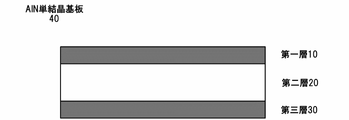
- FIG. 1 is a schematic cross-sectional view showing an example of an AlN single crystal substrate
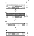
- FIG. FIG. 4 is a cross-sectional view showing a step of forming an AlN single crystal substrate
- 1 is a schematic cross-sectional view showing an example of the configuration of a crystal growth apparatus used in a sublimation method
- the AlN single crystal substrate according to the present invention is composed of one AlN single crystal as a whole, which can be divided in the order of a first layer, a second layer and a third layer in the thickness direction from the viewpoint of defect density. It is an AlN single crystal substrate having a layer structure.
- the second layer has a defect density that is 10 times or more the defect density of each of the first and third layers. In this way, by making the defect density in the inside (second layer) higher than the defect density in each of the surface (first layer) and the back surface (third layer), cracks occurring in the AlN single crystal substrate are suppressed. be able to.
- a deep ultraviolet light emitting device obtained using such an AlN single crystal substrate can improve its yield and luminous efficiency.
- a three-layer AlN single crystal substrate composed of one AlN single crystal as a whole which can be divided in the order of a first layer, a second layer, and a third layer in the thickness direction from the viewpoint of defect density
- the first layer, the second layer, and the third layer An AlN single crystal substrate that can be conveniently or conceptually divided into three layers of layers (these may be referred to as three layered regions, the first region, the second region and the third region, if desired).
- the second layer is only a layer between the first layer and the third layer, for example, the second layer is not located in the depth near the center of the AlN single crystal substrate, It may be located near and far from the third layer, or vice versa.
- the thickness of the second layer may also be as thin as about 10% of the thickness of the entire AlN single crystal substrate. Also, by measuring the AlN single crystal substrate as follows, it can be classified into three layers according to the degree of defect density.
- the defect density in the thickness direction of the AlN single crystal substrate can be measured.
- the single crystal substrate is polished by a predetermined thickness (for example, 1/10 of the thickness of the single crystal substrate, or 30 ⁇ m). Repeat the operation of measuring the defect density on the exposed surface to obtain the defect density distribution in the thickness direction.
- a region in the thickness direction from the surface with the highest defect density inside the AlN single crystal to the surface with a defect density of 1/10 or less of the defect density is defined as a second layer, and the first layer and the second layer Identify the layer boundary and the boundary between the second and third layers.
- each layer (first layer/second layer/third layer) of the AlN single crystal substrate can be divided.
- the defect density of each of the first layer and the third layer means the defect density reaching the surface of the first layer and the third layer facing the second layer
- the defect density of the second layer is , means the highest defect density in the distribution of defect densities inside the AlN single crystal.
- the defect density of each of the first and third layers is the defect density of the second layer (the maximum defect density inside the AlN single crystal measured by the above method). On the other hand, it is 1/10 or less.
- AlN single crystals are known as base substrates for deep ultraviolet light emitting devices, and AlN single crystals with a low defect density have been developed, as disclosed in Patent Document 1, for example.
- the AlN single crystal substrate is likely to crack in the conventional method, and the yield of the deep ultraviolet light emitting device manufactured using such a substrate is low, and the luminous efficiency is also lowered. This is because, for example, in Patent Document 1, the defect density is low on the surface of the AlN single crystal, while it is high on the inside and on the back surface, and the distribution of defects is vertically asymmetrical, so that strain occurs in the AlN single crystal.
- the thickness of the entire AlN single crystal substrate is particularly limited as long as it is possible to obtain a substrate having a three-layer structure in which the internal defect density is higher than the defect density of each of the front and back surfaces and is composed of one AlN single crystal as a whole. Although not limited, it is typically 250-1500 ⁇ m, more typically 400-1500 ⁇ m.
- the first, second and third layers that constitute the AlN single crystal substrate are AlN single crystals and can be said to be orientation layers.
- the AlN single crystal in the present invention refers to those oriented in both the c-axis direction and the a-axis direction, including mosaic crystals.
- Mosaic crystals are aggregates of crystals that do not have distinct grain boundaries but have crystal orientations that are slightly different from one or both of the c-axis and a-axis.
- Such an oriented layer has a structure in which the crystal orientations are substantially aligned in the substantially normal direction (c-axis direction) and the in-plane direction (a-axis direction). With such a structure, it is possible to form a semiconductor layer having excellent quality, particularly excellent orientation, thereon. That is, when the semiconductor layer is formed on the orientation layer, the crystal orientation of the semiconductor layer generally follows the crystal orientation of the orientation layer. Therefore, it is possible to use the semiconductor film formed on the AlN single crystal substrate as the orientation film.
- the AlN single crystal substrate according to the present invention is composed of one AlN single crystal as a whole, which can be divided in the order of the first layer, the second layer, and the third layer in the thickness direction from the viewpoint of defect density. It is an AlN single crystal substrate having a layer structure.
- An example of this AlN single crystal substrate is shown in FIG.
- the AlN single crystal substrate 40 of this embodiment includes a first layer 10, a second layer 20, and a third layer 30.
- the first layer 10, the second layer 20, and the third layer 30 are layers made of AlN single crystal, and the off angle is preferably 0.0 to 4° from the [0001] axis, and 0 from the [0001] axis. 0.2 to 2° is more preferred.
- the first layer 10 is provided on one surface of the second layer 20
- the third layer 30 is provided on the surface of the second layer 20 facing the first layer 10 .
- the AlN crystals of the first layer 10, the second layer 20 and the third layer 30 are oriented in both the c-axis direction and the a-axis direction.
- the orientation evaluation method is not particularly limited, but for example, a known analysis method such as an EBSD (Electron Back Scatter Diffraction Patterns) method or an X-ray pole figure can be used.
- EBSD Electro Back Scatter Diffraction Patterns
- X-ray pole figure X-ray pole figure
- the film is oriented along two axes, the c-axis and the a-axis.
- the substantially in-plane direction of the plate may be oriented in a specific direction (for example, the a-axis) orthogonal to the c-axis.
- the AlN single crystal may be oriented biaxially in the substantially normal direction and the substantially in-plane direction, but the substantially normal direction is preferably oriented along the c-axis.
- the smaller the tilt angle distribution in the substantially normal direction and/or the substantially in-plane direction the smaller the mosaic property of the AlN single crystal. Therefore, from the viewpoint of the crystallinity of the AlN single crystal, the tilt angle distribution is preferably small both in the normal direction and in the plate plane direction, for example ⁇ 5° or less, and more preferably ⁇ 3° or less.
- the second layer 20 has a defect density ten times or more that of each of the first layer 10 and the third layer 30 .
- the defect density of the second layer 20 is the highest defect density inside the AlN single crystal substrate, and the defect densities of the first layer 10 and the third layer 30 are the same as those of the first layer 10 and the third layer 30. , refers to the defect density reaching the surface on the side facing the second layer 20 (in other words, the surface and the back surface of the AlN single crystal substrate).
- the defect density of the second layer 20 is preferably 100 times or more, more preferably 1000 times or more, and still more preferably 100000 times or more that of each of the first layer 10 and the third layer 30 .
- the upper limit of this value is not particularly limited as long as the defect density inside the AlN single crystal substrate is higher than the defect density of each of the front and back surfaces, but is typically 1000000000 times or less. Within such a range, cracks occurring in the AlN single crystal substrate can be more effectively suppressed.
- the defect densities of the first layer 10, the second layer 20, and the third layer 30 can be evaluated by the following known method. Examples of evaluation methods include X-ray topography measurement, etch pit evaluation using KOH melt etching, TEM observation, and combinations thereof. For example, when evaluating the defect densities of the first layer 10 and the third layer 30 using X-ray topography, measurements may be made from the front and rear surfaces of the AlN single crystal substrate. Further, the single crystal substrate is polished by a predetermined thickness (for example, 1/10 of the thickness of the single crystal substrate or 30 ⁇ m), and the defect density of the surface that appears due to polishing is etched using molten KOH etching.
- a predetermined thickness for example, 1/10 of the thickness of the single crystal substrate or 30 ⁇ m
- the operation of performing pit evaluation can be repeated and the highest defect density can be taken as the defect density of the second layer 20 . Further, from the defect density distribution in the thickness direction obtained by such operations, the thickness from the surface with the highest defect density in the AlN single crystal to the surface where the defect density is 1/10 or less than the defect density
- Each layer of the AlN single crystal substrate (first layer/second layer / third layer) can be divided.
- the defect density in the second layer 20 can be rephrased as a layer having a defect density 10 times or more higher than the defect density reaching the surfaces of the first layer 10 and the third layer 30 on any surface thereof.
- the defect density in each layer does not need to be uniform in the thickness direction, and may have a distribution as long as the defect density numerical range described above is satisfied.
- the defect density is preferably measured in the entire area of the surface exposed by polishing for each predetermined thickness.
- the etch pit density can be measured by measuring the surface after etching with an optical microscope, laser microscope, SEM, or the like.
- the N surface which is the surface of the first layer or the third layer, has lower chemical resistance than the facing Al surface, so etch pit evaluation cannot be performed.
- the sample is processed so that the surface at a position of 30 ⁇ m from the N surface is exposed, and the etch pit evaluation is performed on the Al surface on the surface.
- the results obtained can be substituted for the density of defects reaching the surface of the first layer or the third layer.
- the range of defect densities that can be applied to the defect evaluation method is limited, and when the defect density is high, it is preferable to evaluate by TEM observation. Since it is difficult to measure the entire surface region in TEM observation, defects can be evaluated by sampling a 50 ⁇ m ⁇ 50 ⁇ m region including the center of gravity of the AlN single crystal substrate from the surface exposed by polishing and measuring with TEM. can.
- defects include threading screw dislocations (TSD), threading edge dislocations (TED), basal plane dislocations (BPD), and mixed dislocations. Threading means that the dislocation lines are substantially parallel to the [0001] axis of the hexagonal crystal system. Basal means that the dislocation lines lie in the basal hexagonal (0001) plane.
- the ratio of the thickness of the second layer 20 to the thickness of the AlN single crystal substrate is preferably 0.02 to 0.28, more preferably 0.02 to 0.18, still more preferably is between 0.04 and 0.18.
- the thickness of the second layer is preferably 1.0 to 200 ⁇ m, more preferably 10 to 150 ⁇ m, still more preferably 30 to 100 ⁇ m. Within such a range, cracks occurring in the AlN single crystal substrate can be more effectively suppressed.
- Each of the first layer 10 and the third layer 30 preferably has a defect density of 1.0 ⁇ 10 5 /cm 2 or less, more preferably 1.0 ⁇ 10 4 /cm 2 or less.
- the defect density and defect distribution are controlled such that the defect density inside the AlN single crystal substrate is higher than the defect density on each of the front and back surfaces. It is possible to more effectively suppress cracks that occur in the
- the arithmetic mean roughness Ra of the surfaces of the first layer 10 and/or the third layer 30 is preferably 1 nm or less, more preferably 0.5 nm or less, and even more preferably 0.2 nm or less.
- One side of the AlN single crystal substrate preferably has an area of 20 cm 2 or more, more preferably 70 cm 2 or more, and still more preferably 170 cm 2 or more.
- the area of the AlN single crystal substrate By increasing the area of the AlN single crystal substrate in this way, it is possible to increase the area of the semiconductor layer formed thereon. Therefore, it is possible to obtain a large number of semiconductor elements from one semiconductor layer, which is expected to reduce the manufacturing cost.
- the upper limit of the size is not particularly limited, it is typically 710 cm 2 or less on one side.
- the AlN single crystal substrate of the present invention can be manufactured by various manufacturing methods. For example, (a) an alignment precursor layer forming step and (b) a heat treatment step, optionally (c) a process such as grinding or polishing to expose the surface of the alignment layer, and ( d) It can be produced preferably by repeating at least one of the above steps (a) to (c).
- the orientation precursor layer (b) becomes an AlN single crystal by the heat treatment step, and may contain other components such as a dopant.
- the manufacturing process of the AlN single crystal substrate will be described below with reference to FIG. 2, the AlN single crystal substrate of the present invention is not particularly limited to these manufacturing processes, and can be manufactured using a known method. can.
- an AlN single crystal is prepared as the second layer 20, and after forming the orientation precursor layer 11 on one surface of the second layer 20 (see FIG. 2(a)), the first layer 10 is (see FIG. 2(b)), and after forming an alignment precursor layer (not shown) on the surface of the second layer 20 facing the first layer, the alignment precursor layer is subjected to a heat treatment step to form a third layer. It is formed as a layer 30 (see FIG. 2(d)) to produce an AlN single crystal substrate.
- the manufacturing process of the c-axis oriented AlN single crystal substrate will be described below, but the plane orientation is not limited and may be a-axis orientation or r-axis orientation.
- Step of forming an alignment precursor layer (see FIG. 2(a))
- the c-axis oriented AlN single crystal 20 that will eventually become the second layer 20 is prepared, and the oriented precursor layer 11 is formed on one surface (for example, the Al surface) of the AlN single crystal 20. to obtain the laminate 21 .
- a known method can be employed as a method for forming the alignment precursor layer 11.
- a solid-phase film formation method such as an AD (aerosol deposition) method and a HPPD (supersonic plasma particle deposition method) method, a sputtering method, and a vapor deposition method.
- a technique of forming an oriented precursor layer directly on the AlN single crystal 20 can be used.
- CVD method for example, a thermal CVD method, a plasma CVD method, a mist CVD method, an MO (organometal) CVD method, or the like can be used.
- orientation precursor layer 11 a polycrystal prepared in advance by a sublimation method, various CVD methods, sintering, or the like may be used and placed on the AlN single crystal 20.
- orientation precursor layer 11 may be a tape compact produced by tape molding, or a powder compact produced by pressure molding such as uniaxial pressing.
- (b) Epitaxial growth may occur on the AlN single crystal 20 to form the first layer 10 without undergoing the heat treatment step.
- (a) the orientation precursor layer forming step and (b) the heat treatment step can be combined. That is, since the sublimation method is performed at a high temperature, the heat can be used to simultaneously form the alignment precursor layer and generate the single crystal layer from the alignment precursor layer.
- the alignment precursor raw material powder can be molded to produce the alignment precursor layer.
- the orientation precursor layer is a press molding.
- the press-formed body can be produced by press - molding the raw material powder of the orientation precursor based on a known technique. It may be produced by pressing with a pressure of up to 300 kgf/cm 2 .
- the molding method is not particularly limited, and in addition to press molding, tape molding, extrusion molding, cast molding, doctor blade method, and any combination thereof can be used.
- additives such as a binder, a plasticizer, a dispersant, and a dispersion medium are appropriately added to the raw material powder to form a slurry, and the slurry is passed through a thin slit-shaped discharge port to form a sheet.
- Dispensing and molding are preferred.
- the thickness of the sheet-shaped molding is not limited, it is preferably 5 to 500 ⁇ m from the viewpoint of handling.
- a thick orientation precursor layer is required, a large number of such sheet moldings may be stacked to obtain a desired thickness.
- the compact may contain additives such as a sintering aid in addition to the AlN raw material.
- additives such as a sintering aid in addition to the AlN raw material.
- the method of using a prefabricated polycrystal as the orientation precursor layer in order to increase the adhesion between the polycrystal and the AlN single crystal 20, it is necessary to sufficiently smooth the surface of the polycrystal. preferably.
- a method of forming a direct alignment precursor layer using a vapor phase deposition method particularly a sublimation method, a HVPE method, or an MOCVD method is preferred.
- a film can be formed at high speed.
- epitaxial growth may occur on the AlN single crystal 20 without undergoing the (b) heat treatment step, and the first layer 10 may be formed.
- the sublimation method is the most widely studied method for growing bulk AlN that enables the production of AlN single crystal substrates.
- FIG. 3 shows an example of a crystal growth apparatus used in the sublimation method.
- a film forming apparatus 50 shown in FIG. 3 includes a crucible 54, a heat insulating material 56 for insulating the crucible 54, and a coil 58 for heating the crucible 54 to a high temperature.
- the crucible 54 contains AlN as a raw material powder in its lower part, and has a substrate 52 (in this case, the AlN single crystal 20) on which a sublimate of the AlN raw material powder is deposited on its upper part.
- the interior of the crucible 54 is pressurized in an N2 atmosphere, and the crucible 54 is heated by the coil 58 to sublimate the AlN raw material powder.
- the pressure is preferably 10-100 kPa, more preferably 20-90 kPa.
- a temperature gradient is provided so that the temperature near the substrate 52 in the upper portion of the crucible 54 is lower than the temperature in the vicinity of the AlN raw material powder in the lower portion of the crucible 54 .
- the portion of the crucible 54 near the AlN raw material powder is preferably heated to 1900 to 2250°C, more preferably 2000 to 2200°C, and the portion of the crucible 54 near the substrate 52 is heated to 1400 to 2150°C.
- the temperature of the portion near the substrate 52 is preferably 100 to 500.degree.
- the heating is preferably maintained for 2 to 100 hours, more preferably 4 to 90 hours.
- Temperature control can be performed by measuring the temperature of the upper and lower portions of the crucible 54 with a radiation thermometer (not shown) through holes in the heat insulating material 56 covering the crucible 54 and feeding back the temperature.
- the AlN single crystal 20 is arranged as the substrate 52, and AlN is reprecipitated on the surface to form an oriented precursor layer or a single crystal layer.
- the laminate 21 in which the orientation precursor layer 11 is laminated or placed on the AlN single crystal 20 is heat treated to generate the first layer 10 which is the AlN single crystal layer.
- the heat treatment method is not particularly limited as long as epitaxial growth occurs using the AlN single crystal 20 as a seed, and it can be performed in a known heat treatment furnace such as a tubular furnace or a hot plate. In addition to these normal pressure (pressless) heat treatments, pressure heat treatments such as hot pressing and HIP, and combinations of normal pressure heat treatments and pressure heat treatments can also be used.
- the heat treatment atmosphere can be selected from vacuum, nitrogen, and inert gas atmospheres.
- the heat treatment temperature is preferably 1700-2400.degree.
- the heat treatment temperature is preferably 1700° C. or higher, more preferably 1850° C. or higher, and even more preferably 2000° C. or higher.
- the heat treatment temperature is preferably 2350° C. or lower, more preferably 2300° C. or lower.
- the heat treatment temperature and holding time are related to the thickness of the AlN single crystal layer produced by epitaxial growth, and can be appropriately adjusted.
- the surface pressure is preferably 50 kgf/cm 2 or more, more preferably 100 kgf/cm 2 or more, and particularly preferably 200 kgf/cm 2 or more, with no particular upper limit.
- the firing temperature is not particularly limited as long as sintering and epitaxial growth occur, but is preferably 1700° C. or higher, more preferably 1800° C. or higher, and even more preferably 2000° C. or higher.
- the atmosphere during firing can be selected from vacuum, nitrogen, or a mixed gas of nitrogen and inert gas.
- the AlN powder as a raw material is preferably composed of AlN particles having an average particle size of 0.01 to 5 ⁇ m.
- the average particle diameter refers to the average value obtained by observing the powder with a scanning electron microscope and measuring the unidirectional maximum diameter of 100 primary particles.
- An alignment precursor layer 11 or a poorly oriented or non-oriented surface layer may exist or remain on the first layer 10 produced through the above steps (a) and (b).
- it is preferable to expose the surface of the alignment layer by performing processing such as grinding or polishing on the side derived from the alignment precursor layer 11 as necessary.
- a technique for removing the alignment precursor layer 11 and the surface layer is not particularly limited, but examples thereof include a technique of grinding and polishing and a technique of ion beam milling. Polishing of the surface of the first layer is preferably performed by lapping using abrasive grains or chemical mechanical polishing (CMP).
- the third layer 30 can be formed by performing the above (a) to (c) again on the surface of the second layer 20 facing the first layer 10 formed on the second layer 20 . That is, on the surface of the second layer 20 facing the first layer 10 formed on the second layer 20, an alignment precursor layer (not shown) is formed by the same method as in (a) above, and The third layer 30 can be formed by the same method as in (b), and the surface of the alignment layer can be exposed by the same method as in (c), if necessary.
- the orientation precursor layer 11 is formed on the AlN single crystal 20 and heat-treated to form the first layer 10, and then ii) another orientation precursor
- the third layer 30 can be formed by forming a layer (not shown) on the surface of the AlN single crystal 20 facing the first layer and heat-treating.
- the alignment precursor layers may be formed on both surfaces of the second layer 20, and the first layer 10 and the third layer 30 may be formed simultaneously in one heat treatment step (b).
- Such a method is preferable in consideration of quality such as warping of the crystal substrate.
- the c-axis oriented AlN single crystal prepared first may be used as the third layer 30, and AlN single crystals may be formed on one surface thereof in the order of the second layer 20 and the first layer 10, with a predetermined defect density.
- the method of manufacturing the AlN single crystal substrate is no limitation to the method of manufacturing the AlN single crystal substrate as long as it satisfies the numerical range.
- the formation method of each layer so as to satisfy the defect density relationships of the first layer 10, the second layer 20 and the third layer 30 described above.
- (b) heat treatment An AlN single crystal layer may be formed by epitaxial growth on the underlying layer (for example, on the AlN single crystal 20 or on the SiC single crystal substrate) without going through the process.
- the formation of the alignment precursor layer and the heat treatment can be combined, which is preferable in terms of production cost.
- the crystallinity of the obtained AlN single crystal layer is easily affected by the underlying layer.
- the defect density can be gradually reduced as the AlN single crystal layer grows. Although the reason for this is not clear, it is presumed that pair annihilation of defects tends to proceed with crystal growth. However, when such a technique is used, if the AlN single crystal layer is thin, the defect density of the underlying layer is likely to be inherited, so it is necessary to grow the AlN single crystal layer thick in order to reduce the defect density.
- the defect density can be increased by introducing impurities or heterogeneous phases into the AlN single crystal layer by controlling the composition of the orientation precursor layer, ion implantation, or the like.
- impurities to be introduced include Mg, Al, N, Si, H, C, W, B, Zn, Ti, Be, and Ca, preferably Mg, Al, N, and Si.
- the AlN single crystal substrate of the present invention it is preferable to appropriately control the relationship between the defect densities of the first layer 10, the second layer 20 and the third layer 30 by combining the above methods. .
- Example 1 (1) Fabrication of AlN Single Crystal Substrate (1a) Fabrication of AlN Single Crystal A crucible is used as a crystal growth vessel, a SiC substrate is placed as a base material in the crucible, and the AlN raw material powder is placed so as not to come into contact with the SiC substrate. I put it in.
- the holding time was 10 hours.
- the plate surface was further smoothed by lapping using diamond abrasive grains. After that, it was mirror-finished by chemical mechanical polishing (CMP) using colloidal silica. Thus, an AlN single crystal was produced. At this time, the surface of the AlN single crystal on the side in contact with SiC was the rear surface, and the surface opposite to the rear surface was the front surface. When EBSD measurement was performed on the front and back surfaces of this AlN single crystal, it was found that the AlN crystal was oriented in both the c-axis direction and the a-axis direction.
- CMP chemical mechanical polishing
- Examples 2-5 and 8 An AlN single crystal substrate was produced in the same manner as in Example 1, except that the holding times in (1b) and (1c) above and the polishing amount in (1b) above were as shown in Table 1.
- Example 6 (Comparison) An AlN single crystal was produced by the same method as in (1a) above, and an AlN layer was formed thereon by the same method as in (1b) above without grinding the back surface (however, the AlN layer was polished). An additional AlN layer was formed on the AlN layer in the same manner as in (1b) above. Table 1 shows the holding time and the polishing amount of the AlN layer formed directly on the AlN single crystal. Thus, an AlN single crystal substrate was obtained in which an AlN layer was formed on the surface of the AlN single crystal in two stages.
- Example 7 (Comparison) The same method as in Example 1 except that the holding time in (1a) was 25 hours, the holding times in (1b) and (1c), and the polishing amount in (1b) were as shown in Table 1. was used to prepare an AlN single crystal substrate.
- the defect density distribution inside the AlN single crystal was evaluated, and the maximum value of the defect density was 8.0 ⁇ 10 5 cm ⁇ 2 .
- the defect density inside the AlN single crystal was 10 times or more higher than the defect densities on the front surface and the back surface, respectively, and it was determined that the structure had a three-layer structure including the second layer with a high defect density.
- the maximum defect density inside the AlN single crystal was taken as the defect density of the second layer.
- the thickness from the surface with the maximum defect density to the surface with a defect density of 1/10 of the defect density was 30 ⁇ m on the front side and 30 ⁇ m on the back side, so 60 ⁇ m including the surface with the maximum defect density.
- the layer on the surface side from the second layer was the first layer
- the layer on the back side from the second layer was the third layer.
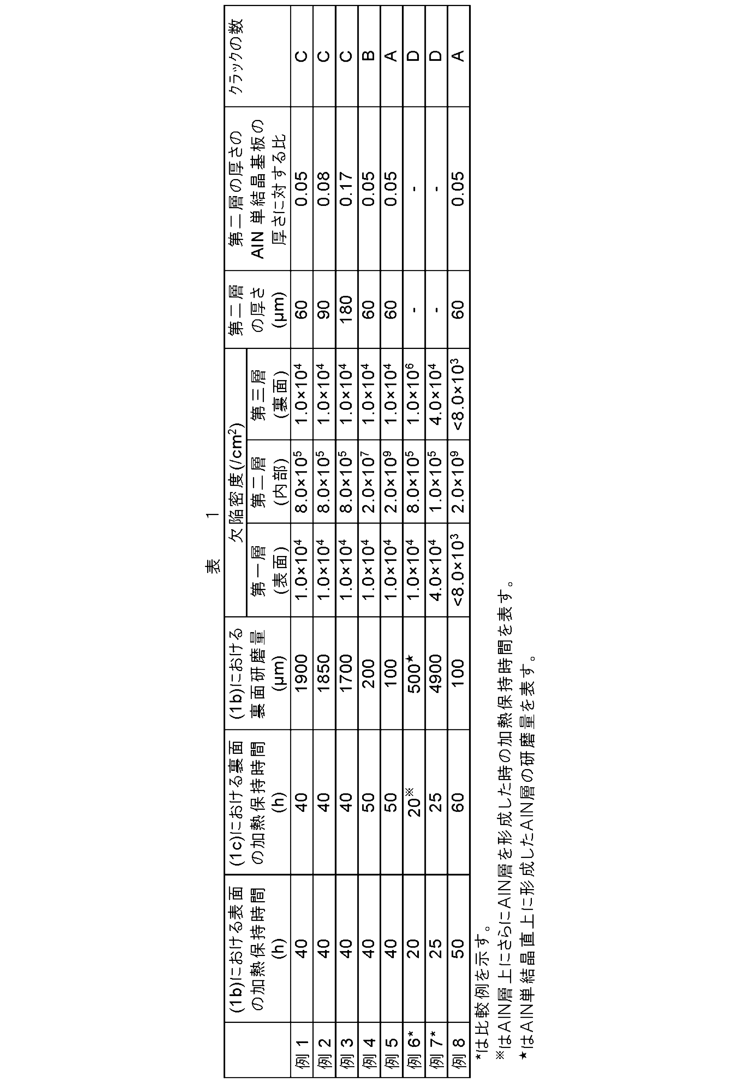
- Table 1 shows the defect densities of the first to third layers and the ratio of the thickness of the second layer to the thickness of the AlN single crystal substrate.
- Example 2-5 Measurements were taken as in Example 1.
- Table 1 shows the defect densities of the first to third layers and the ratio of the thickness of the second layer to the thickness of the AlN single crystal substrate.
- Example 6 (Comparison) Measurements were taken as in Example 1. When the obtained defect density was confirmed, it was 1.0 ⁇ 10 4 cm ⁇ 2 on the front surface, 1.0 ⁇ 10 6 cm ⁇ 2 on the rear surface, and the maximum value inside the AlN single crystal was 8.0 ⁇ 10 5 cm ⁇ 2 . was 2 . It was found that the maximum value of the internal defect density was not 10 times or more the defect densities of the front surface and the back surface, respectively, and that the substrate did not have a three-layer structure like the AlN single crystal substrate of the present invention.
- Example 7 (Comparison) Measurements were taken as in Example 1. When the obtained defect density was confirmed, it was 4.0 ⁇ 10 4 cm ⁇ 2 on the front surface, 4.0 ⁇ 10 4 cm ⁇ 2 on the back surface, and the maximum value inside the AlN single crystal was 1.0 ⁇ 10 5 cm ⁇ 2 . was 2 . It was found that the maximum value of the internal defect density was not 10 times or more the defect densities of the front surface and the back surface, respectively, and that the substrate did not have a three-layer structure like the AlN single crystal substrate of the present invention.
- Example 8 Samples with a film thickness of 300 to 400 nm were sampled by focused ion beam (FIB) processing in a 50 ⁇ m ⁇ 50 ⁇ m region including the center of gravity of the front and back surfaces of the AlN single crystal substrate and 50 ⁇ m ⁇ 50 ⁇ m regions at four other locations. After that, the defect density was measured and evaluated by TEM (manufactured by Hitachi High-Tech Co., Ltd., H-9000UHR). Since no defect was observed on both the front surface and the back surface, it was determined that any region was below the detection limit, that is, the defect density was less than 8.0 ⁇ 10 3 cm ⁇ 2 .
- TEM manufactured by Hitachi High-Tech Co., Ltd., H-9000UHR
- Example 1 when the defect density distribution inside the AlN single crystal was evaluated in the same manner as in Example 1, it was found that the surface with a defect density of 2.0 ⁇ 10 9 cm ⁇ 2 (defect density the highest plane) was observed. In addition, in the thickness direction from that surface, the defect density on the surface of 30 ⁇ m on the front side and the surface of 30 ⁇ m on the back side is 1/10 of the highest defect density, so the thickness of the second layer was found to be 60 ⁇ m. Table 1 shows the defect densities of the first to third layers and the ratio of the thickness of the second layer to the thickness of the AlN single crystal substrate.
- Post-process generally refers to slicing, cutting, dicing, slicing, cutting, dicing, etc. so that a desired semiconductor film can be obtained on the surface (first layer) used for epitaxially growing a semiconductor film for a deep ultraviolet light emitting device. It includes a process of grinding and polishing, a process of actually producing a deep ultraviolet light emitting device, and the like. As a post-process, grinding, polishing and dicing were performed on the surface of the first layer. This post-process was performed on a total of 10 AlN single crystal substrates.
Landscapes
- Chemical & Material Sciences (AREA)
- Engineering & Computer Science (AREA)
- Materials Engineering (AREA)
- Metallurgy (AREA)
- Organic Chemistry (AREA)
- Crystallography & Structural Chemistry (AREA)
- Inorganic Chemistry (AREA)
- Chemical Kinetics & Catalysis (AREA)
- Mechanical Engineering (AREA)
- Crystals, And After-Treatments Of Crystals (AREA)
Abstract
Description
前記第二層が、前記第一層及び前記第三層の各々の欠陥密度の10倍以上の欠陥密度を有する、AlN単結晶基板が提供される。
本発明によるAlN単結晶基板は、欠陥密度の観点から厚み方向に第一層、第二層及び第三層の順に区分可能な、全体として1つのAlN単結晶で構成される3層構成のAlN単結晶基板である。そして、第二層が、第一層及び第三層の各々の欠陥密度の10倍以上の欠陥密度を有する。このように、内部(第二層)の欠陥密度を表面(第一層)及び裏面(第三層)の各々の欠陥密度よりも高くすることで、AlN単結晶基板に発生するクラックを抑制することができる。そして、このようなAlN単結晶基板を用いて得られる深紫外線発光素子は、その歩留まり及び発光効率を向上させることができる。
本発明のAlN単結晶基板は、様々な製造方法により製造することができる。例えば、(a)配向前駆体層の形成工程及び(b)熱処理工程を経ること、所望により(c)研削や研磨等の加工を施して配向層の表面を露出させる工程を経ること、及び(d)上記(a)~(c)の工程のうち少なくとも一つの工程を繰り返すことにより、好ましく製造することができる。ここで、配向前駆体層は、(b)熱処理工程によりAlN単結晶となるものであり、ドーパント等の他の成分を含んでいてもよい。以下ではAlN単結晶基板の製造工程について図2を用いて説明するが、本発明のAlN単結晶基板はこれらの製造工程に特に限定されるものではなく、公知の手法を用いて製造することができる。
図2では、第二層20としてAlN単結晶を用意し、第二層20の一方の表面に配向前駆体層11を形成した後(図2(a)参照)、熱処理工程によって第一層10を形成し(図2(b)参照)、第二層20の第一層と対向する表面に配向前駆体層(図示せず)を形成した後、この配向前駆体層を熱処理工程によって第三層30として形成し(図2(d)参照)、AlN単結晶基板を作製する。c軸配向AlN単結晶基板の製造工程を以下に説明するが、面方位に限定はなく、a軸配向でもよいし、r軸配向でもよい。
配向前駆体層の形成工程では、最終的に第二層20となるc軸配向AlN単結晶20を用意し、そのAlN単結晶20の一方の表面(例えばAl面)に配向前駆体層11を形成し、積層体21を得る。配向前駆体層11の形成方法は公知の手法が採用可能であり、例えば、AD(エアロゾルデポジション)法、HPPD(超音速プラズマ粒子堆積法)法等の固相成膜法、スパッタリング法、蒸着法、昇華法、各種CVD(化学気相成長)法、HVPE法、MBE法、PLD法等の気相成膜法、溶液成長法(例えばフラックス法)等の液相成膜法が挙げられ、配向前駆体層を直接AlN単結晶20上に形成する手法が使用可能である。CVD法としては、例えば熱CVD法、プラズマCVD法、ミストCVD法、MO(有機金属)CVD法等を用いることができる。また、配向前駆体層11として、予め昇華法や各種CVD法、焼結等で作製した多結晶体を使用し、AlN単結晶20上に載置する方法も用いることができる。あるいは、配向前駆体層11の成形体を予め作製し、この成形体をAlN単結晶20上に載置する手法であってもよい。このような配向前駆体層は、テープ成形により作製されたテープ成形体でもよいし、一軸プレス等の加圧成形により作製された圧粉体でもよい。
熱処理工程では、AlN単結晶20上に配向前駆体層11が積層又は載置された積層体21を熱処理することによりAlN単結晶層である第一層10を生成させる。熱処理方法は、AlN単結晶20を種としたエピタキシャル成長が生じるかぎり特に限定されず、管状炉やホットプレート等、公知の熱処理炉で実施することができる。また、これらの常圧(プレスレス)での熱処理だけでなく、ホットプレスやHIP等の加圧熱処理や、常圧熱処理と加圧熱処理の組み合わせも用いることができる。熱処理の雰囲気は真空、窒素、及び不活性ガス雰囲気から選択することができる。熱処理温度は、好ましくは1700~2400℃である。熱処理温度を高くすることで、例えばAlN単結晶層20を種結晶として配向前駆体層11がc軸及びa軸に配向しながら成長しやすくなる。したがって、熱処理温度は、好ましくは1700℃以上、より好ましくは1850℃以上、さらに好ましくは2000℃以上である。一方、熱処理温度が過度に高いと、AlNの一部が昇華により失われたり、AlNが塑性変形して反り等の不具合が生じたりする可能性がある。したがって、熱処理温度は、好ましくは2350℃以下、より好ましくは2300℃以下である。熱処理温度や保持時間はエピタキシャル成長で生じるAlN単結晶層の厚さと関係しており、適宜調整できる。
上記(a)及び上記(b)の工程を経て作製した第一層10上には、配向前駆体層11又は配向性に劣る若しくは無配向の表面層が存在又は残留しうる。この場合、必要に応じて配向前駆体層11に由来する側の面に研削や研磨等の加工を施して配向層の表面を露出させるのが好ましい。こうすることで第一層の表面に優れた配向性を有する材料が露出することになるため、その上に効果的に半導体層をエピタキシャル成長させることができる。配向前駆体層11や表面層を除去する手法は特に限定されるものではないが、例えば、研削及び研磨する手法やイオンビームミリングする手法を挙げることができる。第一層の表面の研磨は、砥粒を用いたラップ加工や化学機械研磨(CMP)により行われるのが好ましい。
第二層20の、第二層20に形成された第一層10と対向する表面に対し、上記(a)~(c)を再度実施することで第三層30を形成することができる。すなわち、第二層20の、第二層20に形成された第一層10と対向する表面に対し、上記(a)と同様の方法で配向前駆体層(図示せず)を形成し、上記(b)と同様の方法で第三層30を形成し、必要に応じて上記(c)と同様の方法で配向層の表面を露出させることができる。
(1)AlN単結晶基板の作製
(1a)AlN単結晶の作製
結晶成長容器として坩堝を用い、この坩堝内にて、基材としてSiC基板を設置し、これと接触しないようにAlN原料粉末を入れた。成長容器をN2雰囲気下で50kPaで加圧し、高周波誘導加熱により成長容器のAlN原料粉末付近の部分を2100℃に加熱する一方で成長容器のSiC基板付近の部分をそれよりも低い温度(温度差ΔT=200℃)に加熱して保持することにより、SiC基板上にAlNを再析出させた。保持時間は10時間とした。AlNが再析出したSiC基板をAlN単結晶が露出するまで、#2000までの番手の砥石を用いて研削した後、ダイヤモンド砥粒を用いたラップ加工により、板面をさらに平滑化した。その後、コロイダルシリカを用いた化学機械研磨(CMP)により鏡面仕上げを施した。こうして、AlN単結晶を作製した。この際、SiCと接していた側のAlN単結晶の面が裏面、裏面と対向する面を表面とした。このAlN単結晶の表面及び裏面でEBSD測定を実施したところ、AlN結晶がc軸方向及びa軸方向の両方に配向していた。
結晶成長容器として坩堝を用い、この坩堝内に基材として上記(1a)で得られたAlN単結晶を設置し、これと接触しないようにAlN原料粉末を入れた。AlN単結晶はその表面がAlN原料粉末に露出するように設置した。成長容器をN2雰囲気下で50kPaで加圧し、高周波誘導加熱により成長容器のAlN原料粉末付近の部分を2100℃に加熱する一方で成長容器のAlN単結晶付近の部分をそれよりも低い温度(温度差ΔT=200℃)に加熱し、40時間保持することにより、AlN単結晶の表面の上にAlN層を形成した。また、表1に示されるようにAlN単結晶の裏面を所定量研削及び研磨することで、所望の厚さにした。
上記(1b)で得たAlN層を備えるAlN単結晶において、AlN単結晶の、AlN層を形成した面とは逆の面、すなわち裏面を露出した状態で、坩堝にこのAlN単結晶を設置したこと以外は上記(1b)と同様にして、AlN層を形成した。こうして、AlN単結晶の表面及び裏面にAlN層を形成したAlN単結晶基板を得た。
上記(1b)及び(1c)の保持時間、並びに上記(1b)の研磨量を表1に示されるものとしたこと以外は、例1と同様の方法を用いてAlN単結晶基板を作製した。
上記(1a)と同様の方法でAlN単結晶を作製し、その上に上記(1b)と同様の方法でAlN層を形成し裏面を研削することなく(但し、AlN層は研磨した)、さらに上記(1b)と同様の方法でAlN層上に追加でAlN層を形成した。保持時間、及びAlN単結晶直上に形成したAlN層の研磨量は表1に示されるものとした。こうして、AlN単結晶の表面上に2段階でAlN層を形成したAlN単結晶基板を得た。
上記(1a)の保持時間を25hとし、上記(1b)及び(1c)の保持時間、並びに上記(1b)の研磨量を表1に示されるものとしたこと以外は、例1と同様の方法を用いてAlN単結晶基板を作製した。
(2a)各層の欠陥密度
例1
得られたAlN単結晶基板の表面及び裏面の全領域をX線トポグラフィー(株式会社リガク製、XRTmicron)で測定したところ、表面の欠陥密度が1.0×104cm-2、裏面の欠陥密度が1.0×104cm-2あった。次に、表面から30μm研磨したところで、全領域をKOH:NaOH=1:1の重量比で混ぜ450℃に加熱した溶融液に研磨した表面を5分間浸し、エッチングした後に、光学顕微鏡で欠陥密度を測定した。これを繰り返すことで、AlN単結晶内部の欠陥密度分布を評価したところ、欠陥密度の最大値は8.0×105cm-2であった。AlN単結晶内部の欠陥密度が、表面及び裏面それぞれの欠陥密度よりも10倍以上高くなっており、欠陥密度が高い第二層を含む3層構造になっていると判断した。AlN単結晶内部の最大の欠陥密度を第二層の欠陥密度とした。欠陥密度が最大となる面から、その欠陥密度の1/10の欠陥密度となる面までの厚さは表面側に30μm、裏面側に30μmであったため、欠陥密度が最大となる面を含む60μmの領域を第二層、第二層から表面側の層を第一層、第二層から裏面側の層を第三層とした。第一層~第三層の欠陥密度、及び第二層の厚さのAlN単結晶基板の厚さに対する比を表1に示す。
例1と同様に測定した。第一層~第三層の欠陥密度、及び第二層の厚さのAlN単結晶基板の厚さに対する比を表1に示す。
例1と同様に測定した。得られた欠陥密度を確認したところ、表面が1.0×104cm-2、裏面が1.0×106cm-2、AlN単結晶内部の最大値が8.0×105cm-2であった。内部の欠陥密度の最大値が表面及び裏面それぞれの欠陥密度の10倍以上となっておらず、本発明のAlN単結晶基板のような3層構成の構造ではないことがわかった。
例1と同様に測定した。得られた欠陥密度を確認したところ、表面が4.0×104cm-2、裏面が4.0×104cm-2、AlN単結晶内部の最大値が1.0×105cm-2であった。内部の欠陥密度の最大値が表面及び裏面それぞれの欠陥密度の10倍以上となっておらず、本発明のAlN単結晶基板のような3層構成の構造ではないことがわかった。
AlN単結晶基板の表面及び裏面の重心を含む50μm×50μmの領域、並びにその他の4箇所における50μm×50μmの領域にて、集束イオンビーム(FIB)による加工で膜厚300~400nmの試料をサンプリングした後、TEM(株式会社日立ハイテク製、H-9000UHR)により欠陥密度を測定し、評価した。表面、裏面ともに、欠陥が観測されなかったため、いずれの領域も検出限界未満、すなわち欠陥密度が8.0×103cm-2未満であるとした。次に、例1と同様にAlN単結晶内部の欠陥密度分布を評価したところ、表面及び裏面それぞれの欠陥密度の10倍以上となる欠陥密度2.0×109cm-2の面(欠陥密度が最も高い面)が認められた。また、その面から厚さ方向に、表面側に30μmの面及び裏面側に30μmの面における欠陥密度が、最も高い欠陥密度の1/10の欠陥密度になることから、第二層の厚さは60μmであることが分かった。第一層~第三層の欠陥密度、及び第二層の厚さのAlN単結晶基板の厚さに対する比を表1に示す。
AlN単結晶基板を後工程で加工する際に、クラックが入るかどうか目視確認した。「後工程」とは、一般的には、深紫外線発光素子用の半導体膜をエピタキシャル成長させるために用いられる面(第一層)を、所望の半導体膜が得られるようにスライス、切断、ダイシング、研削、及び研磨等する工程や、実際に深紫外線発光素子を作製する工程等を含む。後工程として研削、研磨及びダイシングを、第一層の表面に対して行った。この後工程は、計10個のAlN単結晶基板に対して行った。この10個の基板について、以下の基準で格付け評価した。結果を表1に示す。
<評価基準>
‐評価A:クラックが無かったAlN単結晶基板が9~10個
‐評価B:クラックが無かったAlN単結晶基板が6~8個
‐評価C:クラックが無かったAlN単結晶基板が3~5個
‐評価D:全てのAlN単結晶基板にクラックが見られた
Claims (8)
- 欠陥密度の観点から厚み方向に第一層、第二層及び第三層の順に区分可能な、全体として1つのAlN単結晶で構成される3層構成のAlN単結晶基板であって、
前記第二層が、前記第一層及び前記第三層の各々の欠陥密度の10倍以上の欠陥密度を有する、AlN単結晶基板。 - 前記第二層が、前記第一層及び前記第三層の各々の欠陥密度の100倍以上の欠陥密度を有する、請求項1に記載のAlN単結晶基板。
- 前記第二層が、前記第一層及び前記第三層の各々の欠陥密度の1000倍以上の欠陥密度を有する、請求項1又は2に記載のAlN単結晶基板。
- 前記第一層及び前記第三層の各々が、1.0×10⁵/cm2以下の欠陥密度を有する、請求項1~3のいずれか一項に記載のAlN単結晶基板。
- 前記第一層及び前記第三層の各々が、1.0×10⁴/cm2以下の欠陥密度を有する、請求項1~4のいずれか一項に記載のAlN単結晶基板。
- 前記第二層の厚さの、前記AlN単結晶基板の厚さに対する比が0.02~0.28である、請求項1~5のいずれか一項に記載のAlN単結晶基板。
- 前記第二層の厚さの、前記AlN単結晶基板の厚さに対する比が0.02~0.18である、請求項1~6のいずれか一項に記載のAlN単結晶基板。
- 前記第二層の厚さが1.0~70μmである、請求項1~7のいずれか一項に記載のAlN単結晶基板。
Priority Applications (3)
| Application Number | Priority Date | Filing Date | Title |
|---|---|---|---|
| JP2023508782A JP7650958B2 (ja) | 2021-03-25 | 2022-02-16 | AlN単結晶基板 |
| CN202280016509.8A CN116888311B (zh) | 2021-03-25 | 2022-02-16 | AlN单晶基板 |
| US18/455,054 US12637788B2 (en) | 2021-03-25 | 2023-08-24 | AlN single crystal substrate |
Applications Claiming Priority (2)
| Application Number | Priority Date | Filing Date | Title |
|---|---|---|---|
| JP2021052335 | 2021-03-25 | ||
| JP2021-052335 | 2021-03-25 |
Related Child Applications (1)
| Application Number | Title | Priority Date | Filing Date |
|---|---|---|---|
| US18/455,054 Continuation US12637788B2 (en) | 2021-03-25 | 2023-08-24 | AlN single crystal substrate |
Publications (1)
| Publication Number | Publication Date |
|---|---|
| WO2022201986A1 true WO2022201986A1 (ja) | 2022-09-29 |
Family
ID=83396881
Family Applications (1)
| Application Number | Title | Priority Date | Filing Date |
|---|---|---|---|
| PCT/JP2022/006185 Ceased WO2022201986A1 (ja) | 2021-03-25 | 2022-02-16 | AlN単結晶基板 |
Country Status (4)
| Country | Link |
|---|---|
| US (1) | US12637788B2 (ja) |
| JP (1) | JP7650958B2 (ja) |
| CN (1) | CN116888311B (ja) |
| WO (1) | WO2022201986A1 (ja) |
Cited By (2)
| Publication number | Priority date | Publication date | Assignee | Title |
|---|---|---|---|---|
| WO2024189930A1 (ja) * | 2023-03-16 | 2024-09-19 | 日本碍子株式会社 | AlN単結晶基板及びデバイス |
| JPWO2025052587A1 (ja) * | 2023-09-06 | 2025-03-13 |
Citations (2)
| Publication number | Priority date | Publication date | Assignee | Title |
|---|---|---|---|---|
| JP2008115023A (ja) * | 2006-11-01 | 2008-05-22 | Mie Univ | AlN系III族窒化物単結晶厚膜の作製方法 |
| JP2019151520A (ja) * | 2018-03-02 | 2019-09-12 | 国立大学法人三重大学 | 基板および基板の製造方法 |
Family Cites Families (6)
| Publication number | Priority date | Publication date | Assignee | Title |
|---|---|---|---|---|
| JP5005266B2 (ja) * | 2006-03-02 | 2012-08-22 | 日本碍子株式会社 | AlN結晶の作製方法およびAlN厚膜 |
| JP5230522B2 (ja) * | 2009-05-14 | 2013-07-10 | 株式会社トクヤマ | 積層体の製造方法、および該積層体を有する半導体デバイス |
| JP5989559B2 (ja) * | 2013-02-07 | 2016-09-07 | 京セラ株式会社 | 複合基板 |
| WO2015198492A1 (ja) * | 2014-06-25 | 2015-12-30 | Dowaエレクトロニクス株式会社 | エピタキシャルウェーハの製造方法およびエピタキシャルウェーハ |
| JP6579951B2 (ja) * | 2015-12-25 | 2019-09-25 | 株式会社トクヤマ | 窒化アルミニウム単結晶積層体、該積層体の製造方法、及び該積層体を利用した半導体素子の製造方法 |
| JP7065490B2 (ja) * | 2017-07-21 | 2022-05-12 | 学校法人関西学院 | 単結晶AlNの製造方法、及び、単結晶AlN |
-
2022
- 2022-02-16 JP JP2023508782A patent/JP7650958B2/ja active Active
- 2022-02-16 WO PCT/JP2022/006185 patent/WO2022201986A1/ja not_active Ceased
- 2022-02-16 CN CN202280016509.8A patent/CN116888311B/zh active Active
-
2023
- 2023-08-24 US US18/455,054 patent/US12637788B2/en active Active
Patent Citations (2)
| Publication number | Priority date | Publication date | Assignee | Title |
|---|---|---|---|---|
| JP2008115023A (ja) * | 2006-11-01 | 2008-05-22 | Mie Univ | AlN系III族窒化物単結晶厚膜の作製方法 |
| JP2019151520A (ja) * | 2018-03-02 | 2019-09-12 | 国立大学法人三重大学 | 基板および基板の製造方法 |
Cited By (4)
| Publication number | Priority date | Publication date | Assignee | Title |
|---|---|---|---|---|
| WO2024189930A1 (ja) * | 2023-03-16 | 2024-09-19 | 日本碍子株式会社 | AlN単結晶基板及びデバイス |
| JPWO2025052587A1 (ja) * | 2023-09-06 | 2025-03-13 | ||
| WO2025052587A1 (ja) * | 2023-09-06 | 2025-03-13 | 日本碍子株式会社 | AlN単結晶基板の製造方法及びAlN単結晶基板 |
| JP7894533B2 (ja) | 2023-09-06 | 2026-07-23 | Ngk株式会社 | AlN単結晶基板の製造方法及びAlN単結晶基板 |
Also Published As
| Publication number | Publication date |
|---|---|
| US12637788B2 (en) | 2026-05-26 |
| JP7650958B2 (ja) | 2025-03-25 |
| CN116888311A (zh) | 2023-10-13 |
| CN116888311B (zh) | 2026-07-17 |
| US20230392290A1 (en) | 2023-12-07 |
| JPWO2022201986A1 (ja) | 2022-09-29 |
Similar Documents
| Publication | Publication Date | Title |
|---|---|---|
| JP7461851B2 (ja) | 半導体膜 | |
| US20230392290A1 (en) | AlN SINGLE CRYSTAL SUBSTRATE | |
| US12080551B2 (en) | SiC composite substrate including biaxially oreinted SiC layer and semiconductor device | |
| US11942520B2 (en) | Semiconductor film | |
| JP7177248B2 (ja) | SiC複合基板及び半導体デバイス用複合基板 | |
| JP7587688B2 (ja) | SiC基板及びSiC複合基板 | |
| JP7628960B2 (ja) | SiC基板及びその製法 | |
| JP7320070B2 (ja) | 下地基板及びその製造方法 | |
| JP7744507B2 (ja) | AlN単結晶基板及びデバイス | |
| WO2020195196A1 (ja) | SiC複合基板及び半導体デバイス用複合基板 | |
| JP7756846B2 (ja) | 複合基板及びデバイス | |
| US20260009158A1 (en) | Ain single crystal substrate and device | |
| JP7686016B2 (ja) | SiC基板及びSiC複合基板 | |
| JP7822460B2 (ja) | AlN単結晶基板及びデバイス | |
| US20260009159A1 (en) | AlN SINGLE CRYSTAL SUBSTRATE AND DEVICE | |
| US20250391657A1 (en) | Base substrate | |
| US12480226B2 (en) | AlN single crystal substrate | |
| US20260022494A1 (en) | SiC SUBSTRATE AND SiC COMPOSITE SUBSTRATE | |
| WO2025203572A1 (ja) | 下地基板 | |
| WO2025052587A1 (ja) | AlN単結晶基板の製造方法及びAlN単結晶基板 |
Legal Events
| Date | Code | Title | Description |
|---|---|---|---|
| 121 | Ep: the epo has been informed by wipo that ep was designated in this application |
Ref document number: 22774786 Country of ref document: EP Kind code of ref document: A1 |
|
| WWE | Wipo information: entry into national phase |
Ref document number: 202280016509.8 Country of ref document: CN |
|
| WWE | Wipo information: entry into national phase |
Ref document number: 2023508782 Country of ref document: JP |
|
| NENP | Non-entry into the national phase |
Ref country code: DE |
|
| 122 | Ep: pct application non-entry in european phase |
Ref document number: 22774786 Country of ref document: EP Kind code of ref document: A1 |