WO2022201852A1 - 電子機器、判定システム、判定方法およびプログラム - Google Patents
電子機器、判定システム、判定方法およびプログラム Download PDFInfo
- Publication number
- WO2022201852A1 WO2022201852A1 PCT/JP2022/003347 JP2022003347W WO2022201852A1 WO 2022201852 A1 WO2022201852 A1 WO 2022201852A1 JP 2022003347 W JP2022003347 W JP 2022003347W WO 2022201852 A1 WO2022201852 A1 WO 2022201852A1
- Authority
- WO
- WIPO (PCT)
- Prior art keywords
- power supply
- communication unit
- calculator
- electronic device
- power
- Prior art date
- Legal status (The legal status is an assumption and is not a legal conclusion. Google has not performed a legal analysis and makes no representation as to the accuracy of the status listed.)
- Ceased
Links
Images




Classifications
-
- G—PHYSICS
- G06—COMPUTING OR CALCULATING; COUNTING
- G06F—ELECTRIC DIGITAL DATA PROCESSING
- G06F15/00—Digital computers in general; Data processing equipment in general
- G06F15/02—Digital computers in general; Data processing equipment in general manually operated with input through keyboard and computation using a built-in program, e.g. pocket calculators
Definitions
- the present invention relates to an electronic device, a determination system, a determination method, and a program for determining the authenticity of an electronic device.
- Authenticity determination methods in which authentication labels or hologram stickers are affixed to product exteriors or packaging boxes not only cause the stickers to become dirty or come off, but also pose the risk of the stickers themselves being counterfeited. In some cases, it is difficult to determine whether or not the product is authentic.
- An object is to provide a determination method and a program.
- An electronic device includes: a communication unit that communicates with a communication device; a first power supply that does not supply power to the communication unit; a second power supply that supplies power to the communication unit; a control unit that performs processing for transmitting information indicating that power is being supplied to the communication unit from the second power supply to the communication device via the communication unit.
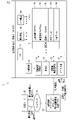
- FIG. 1 is a diagram showing the overall configuration of an authenticity determination system 1 according to an embodiment of the present invention
- FIG. 2 is a block diagram showing the configuration of an electronic circuit of an electronic device (scientific calculator) 10F
- FIG. 2 is a block diagram showing the configuration of an electronic circuit of a communication device (smartphone) 20
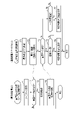
- 6 is a flowchart showing a comparison between electronic device (calculator) confirmation processing by communication device (smartphone) 20 and authentication request handling processing by electronic device (scientific calculator) 10F.
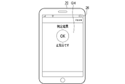
- FIG. 10 is a diagram showing a genuine product determination screen GH for notifying the authenticity determination result “OK” (genuine product) according to the electronic device (calculator) confirmation process by the communication device (smartphone) 20 ;
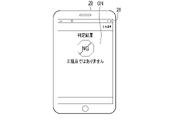
- FIG. 10 is a diagram showing a non-genuine product determination screen GN for notifying the authenticity determination result “NG” (non-genuine product) according to the electronic device (calculator) confirmation process by the communication device (smartphone) 20 .
- 3 is a block diagram showing the configuration of a power supply system for a short-range wireless communication unit (NFC, etc.) 16 of an electronic device (scientific calculator) 10F;
- FIG. 4 is a flowchart showing power supply processing of the short-range wireless communication unit 16 executed by the control unit 13 of the electronic device (scientific calculator) 10F.
- FIG. 1 is a diagram showing the overall configuration of an authenticity determination system 1 according to an embodiment of the present invention.
- the authenticity determination system 1 includes an electronic device (here, a scientific calculator) 10F to be authenticated, a user's communication device (here, a smartphone) 20 for confirming the authenticity of the scientific calculator 10F, and, for example, the manufacturer of the scientific calculator 10F.
- a management server 30 provided on a communication network (here, the Internet) N is included.
- FIG. 2 is a block diagram showing the configuration of the electronic circuit of the electronic device (scientific calculator) 10F.
- FIG. 3 is a block diagram showing the electronic circuit configuration of the communication device (smartphone) 20. As shown in FIG.
- the electronic device is not limited to the scientific calculator 10F, but includes at least a control unit (CPU) 13, a storage unit 14 that stores a small amount of data, an NFC (Near Field Communication) capable of communication connection with the smartphone 20, An electronic device having a short-range wireless communication unit 16 such as Bluetooth Low Energy (registered trademark) or Bluetooth (registered trademark), and a battery power supply (dry battery) DB and a solar power supply (solar battery) SB that supply power to an electronic circuit. are also included (see FIG. 2).
- Control unit 13 includes at least one processor.
- the operating voltage of the functional calculator 10F including the control unit 13 is 1.5V
- the operating voltage of the NFC (non-contact IC tag) used as the short-range wireless communication unit 16 varies depending on the type, and may be 1.65V, 1.8V, 2.5V, or 1.8V. 5V
- the output voltage of the battery power supply DB is 1.5V
- the output voltage of the solar power supply SB is around 2.0V under indoor lighting, 2.0V to 3.0V under cloudy weather, and around 3.0V under fine weather.
- the communication device is not limited to the smartphone 20, but may be configured as a PDA (personal digital assistant), a tablet terminal, a notebook PC (personal computer), a game machine, or the like.
- PDA personal digital assistant
- tablet terminal a tablet terminal
- notebook PC personal computer
- game machine or the like.
- the functional calculator 10F is of a small size that can be held and operated by the user with one hand due to the necessity of its portability.
- the key input unit 11 includes a group of numerical/arithmetic symbol keys 111 for inputting numerical values and formulas and for instructing the execution of calculations, and function functions for inputting various functions and activating memory functions.
- a group of keys 112 a group of mode setting keys 113 for displaying menu screens of various operation modes and instructing the setting of operation modes, operations for moving the cursor and selecting data items displayed on the display unit 12 are performed.
- Cursor keys 114 are provided for doing so.
- the function key group 112 includes the [x-1] (-1 power; reciprocal number) key, the [ ⁇ ] (root) key, the [ ⁇ / ⁇ ] (fraction) key, and the [sin] (sine) key. , [M+] (memory plus) key, [OPTN] (option) key, [RCL] (memory recall) key, etc. are arranged.
- mode setting key group 113 As the mode setting key group 113, a [MODE] (mode) key, a [SHIFT] (shift) key, an [ALPHA] (alphabet) key, an [ON] (power on) key, etc. are arranged.
- the display unit 12 consists of a dot matrix type high resolution liquid crystal display unit.
- the smartphone 20 includes a short-range wireless communication unit 25 such as NFC that can communicate with the scientific calculator 10F, a communication unit 24 that can communicate with the management server 30 via the communication network N, and a touch panel that also functions as a touch input unit.
- a formula display section 26 is provided.
- the scientific calculator 10F has at least the following functions (10a) to (10c) for responding to authenticity requirements.
- a unique ID (for example, , manufacturing serial number) as authentication data to the smartphone 20 that is the source of the authentication data request signal.
- the genuine scientific calculator 10F has a display section 12 consisting of a high-resolution liquid crystal display unit, but can operate at a low operating voltage of 1.5 V. By switching, operation with low power consumption is possible.
- the counterfeit product (non-genuine product) has a high operating voltage of 3.0V and a battery power supply of 3.0V because it does not have the technical capability to operate a high-resolution liquid crystal display unit at an operating voltage as low as 1.5V.
- the counterfeit product has a high operating voltage of 3.0V and a battery power supply of 3.0V because it does not have the technical capability to operate a high-resolution liquid crystal display unit at an operating voltage as low as 1.5V.
- DB Battery power supply
- the smartphone 20 has a calculator confirmation function including at least the following functions (20a) to (20c).
- the authentication data transmitted to the smartphone 20 in response to the reception of the authentication data request signal (specific signal) from the smartphone 20 is not limited to the unique ID (manufacturing serial number) of the scientific calculator 10F. It may be a specific response signal (specific response data) to a specific signal predetermined in the confirmation application 22b.
- the electronic circuit of the electronic device (scientific calculator) 10F includes a key input unit 11, a display unit 12, a battery power supply DB and a solar power supply SB, as well as a control unit (CPU: central processing unit ) 13 , a storage unit 14 , a recording medium reading unit 15 , and a short-range wireless communication unit 16 .
- the CPU 13 has at least one processor.
- the CPU 13 controls the operation of each part of the circuit according to the calculator control program 14a and the authenticity correspondence program 14b stored in the storage unit 14, and receives the key input signal from the key input unit 11 and the proximity signal from the external communication device (for example, the smartphone 20). Various kinds of arithmetic processing are executed according to the reception signal received via the distance wireless communication unit 16 .
- the calculator control program 14a includes programs for executing various calculation processes in response to key input signals from the key input unit 11.
- the authenticity support program 14b includes a program for executing the authentication request support function including at least the functions (10a) to (10c) described above.
- the calculator control program 14a and the authenticity correspondence program 14b may be stored in advance in the storage unit 14, or may be read from an external recording medium M such as a memory card via the recording medium reading unit 15 and stored in the storage unit 14. may have been
- the calculator control program 14a and the authenticity correspondence program 14b cannot be rewritten by the user by operating the key input unit 11. FIG.
- various data storage areas such as a unique ID storage area 14c, a calculation data storage area 14d, and a work data storage area 14e are secured in the storage unit 14.
- unique ID storage area 14c data of a unique ID (manufacturing serial number) unique to each functional calculator 10F is determined, for example, at the time of manufacture by the manufacturer and stored.
- calculation data storage area 14d In the calculation data storage area 14d, data of calculation formulas input according to the operation of the key input unit 11, data of calculation results, and the like are stored.
- the short-range wireless communication unit 16 has a function of short-range wireless communication with an external communication device (for example, the smartphone 20) such as NFC (near field communication) or Bluetooth Low Energy.
- an external communication device for example, the smartphone 20
- NFC near field communication
- Bluetooth Low Energy Bluetooth Low Energy
- control section 13 controls the operation of each circuit section according to the instructions described in the calculator control program 14a and the authenticity correspondence program 14b, and software and hardware cooperate. By working together, it realizes an authenticity request handling function as will be described later in the explanation of the operation.
- the electronic circuit of the communication device (smartphone) 20 includes a control unit (CPU) 21 which is a computer, a storage unit 22, a recording medium reading unit 23, a communication unit 24, and short-range wireless communication. It has a unit 25 , an input unit 27 such as a power key, and a touch panel type display unit 26 .
- the control unit 21 follows the communication device control program 22a and the electronic device confirmation application program (calculator confirmation application) 22b stored in the storage unit 22, and receives input signals corresponding to user operations from the touch panel display unit 26 and the input unit 27. , or a signal received by the communication unit 24 from a communication device on the communication network N, or a signal received from an electronic device (here, the scientific calculator 10F) received via the short-range wireless communication unit 25. control behavior.
- the calculator confirmation application 22b includes a program for executing electronic device (calculator) confirmation functions including at least the functions (20a) to (20c) described above.
- control unit 21 controls the operation of each circuit according to commands described in the communication device control program 22a and the electronic device confirmation application program (calculator confirmation application) 22b.
- the electronic device (calculator) confirmation function described later in the explanation of the operation is realized by the cooperative operation of the hardware.
- FIG. 4 is a flowchart showing a comparison between electronic device (calculator) confirmation processing by the communication device (smartphone) 20 and authentication request handling processing by the electronic device (scientific calculator) 10F.
- FIG. 5 is a diagram showing a genuine product determination screen GH for notifying the authenticity determination result "OK" (genuine product) according to the electronic device (calculator) confirmation process by the communication device (smartphone) 20.
- FIG. 5 is a diagram showing a genuine product determination screen GH for notifying the authenticity determination result "OK" (genuine product) according to the electronic device (calculator) confirmation process by the communication device (smartphone) 20.
- FIG. 6 is a diagram showing a non-genuine product determination screen GN that notifies the authenticity determination result "NG" (non-genuine product) according to the electronic device (calculator) confirmation process by the communication device (smartphone) 20.
- NG non-genuine product
- authentication information for the user to download the electronic device (calculator) confirmation application 22b from the management server 30, which is described in the manual of the electronic device (scientific calculator) 10F, for example.
- the communication device (smartphone) 20 in which the electronic device (calculator) confirmation application 22b is installed is used to check whether the electronic device (scientific calculator) 10F is a genuine product or a non-genuine product. Assume.
- the electronic device (scientific calculator) 10F changes the power supply of the electronic circuit to the battery power supply when the output voltage from the solar power supply SB reaches the specified operating voltage and is maintained for a certain period of time depending on the amount of light striking the solar power supply SB.
- the DB is switched to the solar power source SB, and the display unit 12 displays the solar mark SM (see FIG. 1) indicating the operating state of the solar power source SB (step F1).
- At least the near field communication unit (NFC) 16 does not receive power supply from the battery power supply DB, but only receives power supply from the solar power supply SB to operate.
- the user first confirms that the solar mark SM is displayed on the display unit 12 of the scientific calculator 10F, and confirms that the scientific calculator 10F is in an operating state with the solar power supply SB.
- the control unit 21 communicates with the scientific calculator 10F via the near field communication unit (NFC) 25, and requests authentication data. A signal is transmitted (step T2).
- control unit 21 sends the authentication data transmitted from the scientific calculator 10F in response to the authentication data request signal transmitted in step T2 to the near field communication unit (NFC) 25 within a certain period of time (for example, 3 seconds). (Steps T3, T4).
- the control unit 13 stores the unique ID storage area 14b. (step F3).
- control unit 13 transmits the unique ID (manufacturing serial number “12345678”) acquired in step F3 to the smartphone 20 that requested the authenticity data, which is in communication connection via the near field communication unit (NFC) 16. It is transmitted as data (step F4).
- the unique ID (manufacturing serial number “12345678”) transmitted as the authentication data from the functional calculator 10F within a certain period of time after transmitting the authentication data request signal in step T2 is transmitted to the near field wireless communication unit (NFC ) 25 (step T3 (Yes)), the control unit 21 converts the received unique ID (manufacturing serial number) of the functional calculator 10F into a unique ID (manufacturing serial number) included in the calculator confirmation application 22b. number) (step T5).
- step T6 When it is determined that the received unique ID (manufacturing serial number) of the functional calculator 10F matches the unique ID (manufacturing serial number) included in the calculator confirmation application 22b (step T5 (Yes)), the control unit 21 As shown in FIG. 5, a genuine product determination screen GH showing the result of authenticity determination “OK” and “genuine product” is generated, and displayed on the display unit 26 to prompt the user to confirm the product. It is notified that the functional calculator 10F that has been used is a genuine product (step T6).
- step T3 if it is determined that the unique ID (manufacturing serial number) of the scientific calculator 10F received in step T3 does not match the unique ID (manufacturing serial number) included in the calculator confirmation application 22b (step T5 (No) ), as shown in FIG. 6, the control unit 21 generates a non-genuine product determination screen GN indicating the authenticity determination result “NG” and “not a genuine product”, and displays the non-genuine product determination screen GN on the display unit 26. Then, the user is notified that the scientific calculator 10F to be checked is a non-genuine product (counterfeit product, counterfeit product) (step T7).
- the control unit 21 causes the display unit 26 to display a non-genuine product determination screen GN indicating the result of authenticity determination "NG" and "not a genuine product” to prompt the user to confirm. Notifies that the scientific calculator 10F is a non-genuine product (counterfeit, counterfeit) (step T7).
- the solar mark SM is a fake, the short-range wireless communication unit 16 is not operating, or the short-range wireless communication unit 16 is in the battery power supply DB. It can be determined that the product is a non-genuine product (counterfeit product, counterfeit product) that does not have an authentication request correspondence function (authentication correspondence program 14b) even if it is operating according to the above.
- the genuine scientific calculator 10F operates the near-field wireless communication unit (NFC) 16 only in the operating state of the solar power supply SB displaying the solar mark SM, and the calculator confirmation according to the calculator confirmation application 22b by the smartphone 20.
- NFC near-field wireless communication unit
- the smart phone 20 After confirming that the scientific calculator 10F to be checked is genuine by performing calculator confirmation processing according to the calculator confirmation application 22b on the smartphone 20 and displaying the genuine product determination screen GH, Shield the solar power source SB of the scientific calculator 10F from light with a hand, and in a state in which the solar power source SB does not function (the solar mark SM is not displayed), the smart phone 20 performs the calculator confirmation processing of the scientific calculator 10F again.
- the short-range wireless communication unit 16 of the scientific calculator 10F does not operate due to the interruption of the solar power supply SB, and the solar mark SM is not displayed. Since the data is not received (step T3 (No) ⁇ T4 (Yes) ⁇ T7), the user waits until the display unit 26 displays the non-genuine product determination screen GN (meaning no communication connection in this case). By confirming, it is possible to confirm that the functional calculator 10F to be confirmed is a genuine product and to obtain confirmation thereof from the genuine product determination screen GH displayed according to the previous calculator confirmation processing.
- the electronic device (scientific calculator) 10F has a battery power supply DB and a solar power supply SB, and a near field communication unit (NFC) for communication connection with an external communication device (smartphone) 20 ) 16, the short-range wireless communication unit 16 operates by the solar power supply SB only when the power supply for operating the electronic circuit of the scientific calculator 10F is switched from the battery power supply DB to the solar power supply SB.
- the electronic device (scientific calculator) 10F displays the solar mark SM on the display unit 12 in the operating state of the solar power source SB.
- the user's smartphone 20 uses the electronic device (calculator) confirmation application 22b to check the scientific calculator via the near field communication unit (NFC) 25. 10, the unique ID (manufacturing serial number, etc.) as the authenticity data received from the functional calculator 10 is sent to the calculator confirmation application 22b. etc.), the touch panel display unit 26 displays a genuine product determination screen GH to notify the user that the scientific calculator 10F is a genuine product.
- the user blocks the light incident on the solar power supply SB of the scientific calculator 10F, confirms that the solar mark SM has disappeared, and uses the smartphone 20 to perform the calculator confirmation process again according to the calculator confirmation application 22b.
- communication connection with the short-range wireless communication unit 16 of the scientific calculator 10F cannot be established, and a unique ID as authenticity data is not received from the scientific calculator 10F.
- Check the non-genuine product determination screen GN meaning no communication connection here to confirm that the scientific calculator 10F is a genuine product.
- the solar mark SM is displayed on the scientific calculator 10F
- the unique ID as the authenticity data received by the smartphone 20 from the scientific calculator 10F does not match the unique ID included in the calculator confirmation application 22b, the authenticity
- the smart phone 20 displays the genuine product determination screen GH even though the scientific calculator 10F does not display the solar mark SM, the scientific calculator 10F operates on the battery power source DB. Therefore, it can be confirmed that the scientific calculator 10F is a non-genuine product (counterfeit product, counterfeit product).
- the authenticity determination system 1 of the embodiment while confirming the display state of the solar mark SM on the scientific calculator 10F, the user follows the calculator confirmation process of the smartphone 20 to display the genuine product determination screen GH or the non-genuine product determination screen.
- the display of GN By confirming the display of GN, it is possible to determine the authenticity of the product body with high certainty without using the exterior of the product, the packing box, or the like.
- the authenticity data received from the scientific calculator 10F via the short-range wireless communication unit 25 in a state where the scientific calculator 10F displays the solar mark SM by the calculator confirmation processing by the smartphone 20 is unique.
- ID (manufacturing serial number, etc.) that matches the unique ID (manufacturing serial number, etc.) included in the calculator confirmation application 22b is configured to determine that the functional calculator 10F is genuine.
- the genuine scientific calculator 10F operates the near field wireless communication unit (NFC) 16 only in the operating state of the solar power supply SB displaying the solar mark SM
- the authenticity of the scientific calculator 10F is requested.
- the solar mark SM displayed in response to reception of an authentication data request signal (specific signal) from the smartphone 20, a specific response signal (specific response data) predetermined by the calculator confirmation application 22b is generated.
- the functional calculator 10F can be determined to be genuine without confirming that the unique ID (manufacturing serial number, etc.) of the functional calculator 10F matches.
- the smartphone 20 does not require the authentication information (calculator identification data) of the functional calculator 10F described in the instruction manual of the functional calculator 10F to download the calculator confirmation application 22b.
- the user can install the calculator confirmation application 22b to determine the authenticity of the functional calculator 10F.
- the scientific calculator 10F switches the electronic circuit from the battery power supply DB when the output voltage from the solar power supply SB reaches the operating voltage (specified operating voltage) of the electronic circuit for a certain period of time.
- the function (10a) of switching the power supply of the electronic circuit from the solar power supply SB to the battery power supply DB when the output voltage from the solar power supply SB drops below the specified operating voltage has been described.
- a configuration in which the short-range wireless communication unit 16 operates stably with the solar power supply SB only when the short-range wireless communication unit 16 is switched to the solar power supply SB will be described in more detail with reference to FIGS. 7 and 8 below.
- FIG. 7 is a block diagram showing the configuration of a power supply system for the short-range wireless communication unit (NFC, etc.) 16 of the scientific calculator 10F.
- the control unit (CPU) 13 has a function of detecting the output voltage Vd of the battery power supply DB and the output voltage Vsb of the solar power supply SB.
- the short-range wireless communication unit 16 is supplied with the output voltage Vsb from the solar power supply SB via the power supply switch SW that controls ON/OFF by the control unit 13 to operate or stop the short-range wireless communication unit 16. .
- the output voltage Vsb from the solar power supply SB to the short-range wireless communication unit 16 is temporarily insufficient, the insufficient voltage may be supplemented by the output voltage Vd of the battery power supply DB.
- FIG. 8 is a flowchart showing power supply processing of the short-range wireless communication unit 16 executed by the control unit 13 of the scientific calculator 10F.
- the control unit (CPU) 13 determines whether or not the output voltage Vsb output when the solar power source SB is exposed to light is detected (step S1), and if the output voltage Vsb is detected (step S1 (Yes)). , it is determined whether the output voltage Vsb has reached or exceeded the specified operating voltage Vs (step S2).
- step S1 If the output voltage Vsb of the solar power supply SB is not detected (step S1 (No)) or if the output voltage Vsb of the solar power supply SB has not reached or exceeded the specified operating voltage Vs (step S2 (No)), , when the output voltage Vsb is not supplied to the short-range wireless communication unit 16 (power supply switch SW-OFF) (step S6 (No)), the control unit 13 repeats the process from step S1 (returns). .
- step S1 The output voltage Vsb of the solar power supply SB is detected (step S1 (Yes)), and when it is determined that the output voltage Vsb has reached the specified operating voltage Vs or more (step S2 (Yes)), the control unit 13 outputs It is determined whether or not the state in which the voltage Vsb has reached the specified operating voltage Vs or higher has been maintained for a predetermined time (T: 3 seconds, for example) or longer (step S3).
- step S3 A state in which the output voltage Vsb of the solar power source SB reaches or exceeds the specified operating voltage Vs and is maintained for a certain period of time (T: 3 seconds, for example), that is, a state in which the power supply from the solar power source SB is stably obtained. If determined (step S3 (Yes)), the control unit 13 turns on the power supply switch SW to supply the output voltage Vsb of the solar power supply SB to the short-range wireless communication unit 16, and the short-range wireless communication unit 16 communication operation is enabled (step S4).
- the control unit 13 causes the display unit 12 to display the solar mark SM (see FIG. 1) (step S5).
- Step S7 When the power supply switch SW is turned on and the output voltage Vsb of the solar power supply SB is being supplied to the short-range wireless communication unit 16, the output voltage Vsb is no longer detected because the solar power supply SB is no longer exposed to light. (Step S1 (No) ⁇ S6 (Yes)), or if it is determined that the amount of light impinging on the solar power supply SB has decreased and the output voltage Vsb has dropped below the specified operating voltage Vs (Step S2 (No ) ⁇ S6 (Yes)), the control unit 13 turns off the power supply switch SW to stop supplying the output voltage Vsb from the solar power supply SB to the short-range wireless communication unit 16 (step S7).
- the control unit 13 hides the solar mark SM (see FIG. 1) displayed on the display unit 12 (step S8).
- the output voltage Vsb of the solar power supply SB temporarily drops below the specified operating voltage Vs. If the output voltage Vsb drops significantly (for example, 2 seconds or less), the output voltage Vd of the battery power supply DB is temporarily supplied as an auxiliary until the output voltage Vsb returns to the specified operating voltage Vs.
- the configuration may be such that the operation of the distance wireless communication unit 16 is stabilized.
- the scientific calculator 10F executes power supply processing for the short-range wireless communication unit 16, thereby realizing stable operation of the short-range wireless communication unit 16 by power supply from the solar power supply SB.
- power supply processing of the short-range wireless communication unit 16 is executed by power supply from the solar power source SB.
- the short-range wireless communication unit 16 may be powered by the power supply having the higher output voltage.
- each process by the authenticity determination system 1 described in each of the above embodiments that is, the electronic device (calculator) confirmation process in the communication device (smartphone) 20 and the electronic device (calculator) 10F shown in the flowchart of FIG.
- Each method can be executed by a computer using memory cards (ROM cards, RAM cards, etc.), magnetic disks (floppy (registered trademark) disks, hard disks, etc.), optical discs (CD -ROM, DVD, etc.), semiconductor memory, or other external recording device media for distribution.
- control unit (CPU) of the electronic device reads the program recorded on the medium of the external recording device into the storage device, and the operation of the electronic device described in each embodiment is controlled by the read program.
- CPU control unit
- Calculator A confirmation function and a function for requesting authenticity can be realized, and the same processing can be executed by the method described above.
- program data for realizing each method can be transmitted in the form of program code over the communication network (N), and from a computer device (program server) connected to this communication network (N), It is also possible to load the data of the program into an electronic device and store it in a storage device, thereby realizing the aforementioned electronic device (calculator) confirmation function and authentication request response function.
- the present invention is not limited to the embodiment, and can be variously modified in the implementation stage without departing from the scope of the invention. Further, the embodiments may be implemented in combination as appropriate, in which case the combined effect can be obtained. Furthermore, various inventions are included in the embodiments, and various inventions can be extracted by combinations selected from a plurality of disclosed constituent elements. For example, even if some constituent elements are deleted from all the constituent elements shown in the embodiments, if the problem can be solved and effects can be obtained, the configuration with the constituent elements deleted can be extracted as an invention.
- the present invention is particularly useful for highly reliable authenticity determination of the product itself without using the product's outer packaging or packaging box.
- Authenticity determination system 10F Electronic device (scientific calculator) SB ...Solar power supply (solar battery) SM...Solar mark DB...Battery power source 11...Key input unit 12...Display unit 13...Control unit (CPU) REFERENCE SIGNS LIST 14: storage unit 14a: calculator control program 14b: authenticity correspondence program 14c: unique ID storage area 14d: calculation data storage area 16: short-range wireless communication unit 20: communication device (smartphone/tablet terminal, etc.) 21 ...
- control unit CPU
- Storage unit 22a Communication device control program 22b Electronic device (calculator) confirmation application program 24 Communication unit 25 Near field wireless communication unit 26 Touch panel display unit 30 Management server N Communication network (Web) GH ...Genuine product judgment screen GN ...Non-genuine product judgment screen (meaning no communication connection when solar power SB is blocked) SW ... Power supply switch for the short-range wireless communication unit
Landscapes
- Engineering & Computer Science (AREA)
- Theoretical Computer Science (AREA)
- Computing Systems (AREA)
- Computer Hardware Design (AREA)
- Physics & Mathematics (AREA)
- General Engineering & Computer Science (AREA)
- General Physics & Mathematics (AREA)
- Telephone Function (AREA)
- Power Sources (AREA)
Abstract
製品の外装や梱包箱などを利用することなく、製品本体の確実性の高い真贋判定を行うことが可能になる。関数電卓10Fは、電池電源DBおよびソーラ電源SBと、通信機器(スマートフォン)20と通信接続するための近距離無線通信部(NFC)16とを備え、NFC16は電卓10Fを動作させる電源が電池電源DBからソーラ電源SBに切り替えられた状態でのみソーラ電源SBにより動作する。電卓10Fは、ソーラ電源SBによる動作状態で表示部12にソーラマークSMを表示させる。電卓10FにソーラマークSMが表示された状態で、通信機器20により、電卓確認アプリ22bに従い電卓10に真贋データ要求信号を送信することに応答して、電卓10から受信された固有ID(製造シリアル番号)が電卓確認アプリ22bに含まれる固有ID(製造シリアル番号)と一致すると、表示部26に正規品判定画面GHを表示させ電卓10Fが正規品であると通知する。
Description
本発明は、電子機器の真贋判定を行うための電子機器、判定システム、判定方法およびプログラムに関する。
従来から、あらゆる製品の模倣品対策が重要となっているが、認証ラベルやホログラムのシールを、製品の外装や梱包箱などに貼り付けることで、製品が正規品であることを確認できるようにした真贋判定方法が広く利用されている(例えば、特許文献1参照。)。
認証ラベルやホログラムのシールを製品の外装や梱包箱などに貼り付けて行なう真贋判定方法では、シールの汚れや剥がれだけでなく、シール自体の偽造の恐れもあるため、製品本体が正規品であるか否かの真贋判定を行うことが困難な場合もある。
本発明は、このような課題に鑑みなされたもので、製品の外装や梱包箱などを利用することなく、製品本体の確実性の高い真贋判定を行うことが可能になる電子機器、判定システム、判定方法およびプログラムを提供することを目的とする。
本発明に係る電子機器は、
通信機器と通信する通信部と、
前記通信部には電源を供給しない第1電源と、
前記通信部に電源を供給する第2電源と、
前記第2電源により前記通信部に電源が供給されていることを示す情報を、前記通信部を介して前記通信機器に送信する処理を行なう制御部と、を備える。
通信機器と通信する通信部と、
前記通信部には電源を供給しない第1電源と、
前記通信部に電源を供給する第2電源と、
前記第2電源により前記通信部に電源が供給されていることを示す情報を、前記通信部を介して前記通信機器に送信する処理を行なう制御部と、を備える。
本発明によれば、製品の外装や梱包箱などを利用することなく、製品本体の確実性の高い真贋判定を行うことが可能になる。
以下図面により本発明の実施の形態について説明する。
図1は、本発明の実施形態に係る真贋判定システム1の全体の構成を示す図である。
真贋判定システム1は、真贋判定の対象とする電子機器(ここでは関数電卓)10Fと、関数電卓10Fの真贋を確認するユーザの通信機器(ここではスマートフォン)20と、例えば関数電卓10Fの製造元により通信ネットワーク(ここではインターネット)N上に設けられた管理サーバ30とを含んで構成される。
図2は、電子機器(関数電卓)10Fの電子回路の構成を示すブロック図である。
図3は、通信機器(スマートフォン)20の電子回路の構成を示すブロック図である。
電子機器は、関数電卓10Fに限定されるものではなく、少なくとも、制御部(CPU)13と、少量のデータを記憶する記憶部14と、スマートフォン20と通信接続可能なNFC(Near Field Communication)、Bluetooth Low Energy(登録商標)、Bluetooth(登録商標)などの近距離無線通信部16と、電子回路に電源を供給する電池電源(乾電池)DBおよびソーラ電源(太陽電池)SBと、を有する電子機器も含まれる(図2参照)。
なお、近距離無線通信部16の駆動電圧は、ソーラ電源(太陽電池)SBにより供給される。制御部13は、少なくとも一つのプロセッサを含む。
例えば、制御部13を含む関数電卓10Fの動作電圧は1.5V、近距離無線通信部16とするNFC(非接触ICタグ)の動作電圧は種類により異なり1.65Vや1.8Vや2.5V、電池電源DBの出力電圧は1.5V、ソーラ電源SBの出力電圧は屋内照明下で2.0V前後、曇天下で2.0V~3.0V、晴天下で3.0V前後である。
また、通信機器は、スマートフォン20に限定されるものではなく、PDA(personal digital assistants)、タブレット端末、ノートPC(personal computer)、ゲーム機等として構成され得る。
関数電卓10Fは、その携帯性の必要からユーザが片手で十分把持し片手で操作可能な小型サイズからなり、関数電卓10Fの本体正面にはキー入力部11および表示部12が設けられる。
キー入力部11には、数値や数式を入力したり計算の実行を指示したりするための数値・演算記号キー群111、各種の関数を入力したりメモリ機能を立ち上げたりするための関数機能キー群112、各種動作モードのメニュー画面を表示させたり動作モードの設定を指示したりするためのモード設定キー群113、表示部12に表示されたカーソルの移動操作やデータ項目の選択操作などを行うためのカーソルキー114が備えられる。
数値・演算記号キー群111としては、[0]~[9](数値)キー、[+][-][×][÷](四則記号)キー、[Ans][=](実行)キー、[AC](クリア)キーなどが配列される。
関数機能キー群112としては、[x-1](-1乗;逆数)キーをはじめ、[√□](ルート)キー、[□/□](分数)キー、[sin](サイン)キー、[M+](メモリプラス)キー、[OPTN](オプション)キー、[RCL](メモリ呼び出し)キーなどが配列される。
モード設定キー群113としては、[MODE](モード)キー、[SHIFT](シフト)キー、[ALPHA](アルファベット)キー、[ON](電源オン)キーなどが配列される。
表示部12は、ドットマトリクス型の高解像度液晶表示ユニットからなる。
スマートフォン20は、関数電卓10Fと通信接続可能なNFCなどの近距離無線通信部25と、通信ネットワークNを介して管理サーバ30と通信接続可能な通信部24と、タッチ入力部としても機能するタッチパネル式表示部26を備えている。
<関数電卓10Fの真贋要求対応機能>
関数電卓10Fは、少なくとも以下(10a)~(10c)の機能を含む真贋要求対応機能を備えている。
関数電卓10Fは、少なくとも以下(10a)~(10c)の機能を含む真贋要求対応機能を備えている。
(10a) ソーラ電源SBからの出力電圧が電子回路の動作電圧(規定動作電圧)に到達した状態が一定時間維持された場合に、電子回路の電源を電池電源DBからソーラ電源SBに切り替え、ソーラ電源SBからの出力電圧が規定動作電圧以下に低下した場合に、電子回路の電源をソーラ電源SBから電池電源DBに切り替える機能。
(10b) 電源がソーラ電源SBに切り替えられた状態において、スマートフォン20からの真贋データ要求信号(特定信号)の受信に応じて、記憶部14の固有ID記憶領域14cに記憶された固有ID(例えば、製造シリアル番号)のデータを、真贋データとして真贋データ要求信号の発信元のスマートフォン20へ送信する機能。
(10c) 電源がソーラ電源SBに切り替えられた状態において、ソーラ電源SBによる動作状態であることを表わすソーラマークSMを表示部12に表示させる機能。
なお、正規品の関数電卓10Fは、高解像度液晶表示ユニットからなる表示部12を有しているが、1.5Vの低い動作電圧で動作可能であるため、電池電源DBとソーラ電源SBとを切り替えて、低消費電力化した動作が可能である。
一方、模倣品(非正規品)は、高解像度液晶表示ユニットを1.5Vの低い動作電圧で動作可能にする技術力がないため、動作電圧が3.0Vと高く、3.0Vの電池電源DBで動作する。従って、外観上、ソーラ電源SBを有していても、電源を切り替える機能を備えていない。
<スマートフォン20の電卓確認機能>
スマートフォン20は、少なくとも以下(20a)~(20c)の機能を含む電卓確認機能を備えている。
スマートフォン20は、少なくとも以下(20a)~(20c)の機能を含む電卓確認機能を備えている。
(20a) 例えば通信ネットワークN上のプログラムサーバ(管理サーバ30)からダウンロードしてインストールした電子機器確認アプリケーションプログラム(電卓確認アプリ)22bに従い、NFCなどの近距離無線通信部25を用い、関数電卓10Fに通信接続して真贋データ要求信号を送信する機能。
(20b) 真贋データ要求信号の関数電卓10Fへの送信に応答して同関数電卓10Fから送信された真贋データ(固有ID:製造シリアル番号)を、近距離無線通信部25を用いて受信し、電卓確認アプリ22bに含まれる関数電卓10Fの固有ID(製造シリアル番号)と一致するか否かにより、関数電卓10Fの真贋判定を行う機能。
(20c) 関数電卓10Fの真贋判定結果を表示部26に表示させる機能。
なお、関数電卓20Fにおいて、スマートフォン20からの真贋データ要求信号(特定信号)の受信に応じて当該スマートフォン20へ送信する真贋データは、関数電卓10Fの固有ID(製造シリアル番号)に限らず、電卓確認アプリ22bにおいて予め定められた特定信号に対する特定応答信号(特定応答データ)であってよい。
<電子機器(関数電卓)10Fの電子回路>
図2に示すように、電子機器(関数電卓)10Fの電子回路は、キー入力部11、表示部12、電池電源DBおよびソーラ電源SBに加えて、コンピュータである制御部(CPU:central processing unit)13と、記憶部14と、記録媒体読取部15と、近距離無線通信部16と、を備えている。CPU13は、少なくとも一つのプロセッサを有している。
図2に示すように、電子機器(関数電卓)10Fの電子回路は、キー入力部11、表示部12、電池電源DBおよびソーラ電源SBに加えて、コンピュータである制御部(CPU:central processing unit)13と、記憶部14と、記録媒体読取部15と、近距離無線通信部16と、を備えている。CPU13は、少なくとも一つのプロセッサを有している。
CPU13は、記憶部14に記憶されている電卓制御プログラム14aおよび真贋対応プログラム14bに従い回路各部の動作を制御し、キー入力部11からのキー入力信号および外部の通信機器(例えばスマートフォン20)から近距離無線通信部16を介して受信される受信信号に応じた各種の演算処理を実行する。
電卓制御プログラム14aは、キー入力部11からのキー入力信号に応じて、各種の計算処理を実行するためのプログラムを含む。
真贋対応プログラム14bは、少なくとも前述の(10a)~(10c)の機能を含む真贋要求対応機能を実行するためのプログラムを含む。
電卓制御プログラム14aおよび真贋対応プログラム14bは、記憶部14に予め記憶されていてもよいし、あるいはメモリカードなどの外部記録媒体Mから記録媒体読取部15を介して記憶部14に読み込まれて記憶されたものであってもよい。電卓制御プログラム14aおよび真贋対応プログラム14bは、ユーザがキー入力部11の操作によって書き換えできないようになっている。
記憶部14には、さらに、固有ID記憶領域14c、計算データ記憶領域14dおよび作業データ記憶領域14eなどの各種のデータ記憶領域が確保される。
固有ID記憶領域14cには、個々の関数電卓10Fに固有の固有ID(製造シリアル番号)のデータが、例えば製造元での製造時に決定されて記憶される。
計算データ記憶領域14dには、キー入力部11の操作に応じて入力された計算式のデータ、計算結果のデータなどが記憶される。
作業データ記憶領域14eには、制御部13による各部の動作の制御に応じて生成または取得される各種のデータが必要に応じて一時的に記憶される。
近距離無線通信部16は、NFC(near field communication)、Bluetooth Low Energyなど、外部の通信機器(例えばスマートフォン20)と近距離で無線通信する機能を備える。
このように構成された電子機器としての関数電卓10Fは、制御部13が電卓制御プログラム14aおよび真贋対応プログラム14bに記述された命令に従い回路各部の動作を制御し、ソフトウエアとハードウエアとが協働して動作することにより、後述の動作説明で述べるような真贋要求対応機能を実現する。
<通信機器(スマートフォン)20の電子回路>
図3に示すように、通信機器(スマートフォン)20の電子回路は、コンピュータである制御部(CPU)21と、記憶部22と、記録媒体読取部23と、通信部24と、近距離無線通信部25と、電源キーなどの入力部27と、タッチパネル式表示部26とを備えている。
図3に示すように、通信機器(スマートフォン)20の電子回路は、コンピュータである制御部(CPU)21と、記憶部22と、記録媒体読取部23と、通信部24と、近距離無線通信部25と、電源キーなどの入力部27と、タッチパネル式表示部26とを備えている。
制御部21は、記憶部22に記憶されている通信機器制御プログラム22aおよび電子機器確認アプリケーションプログラム(電卓確認アプリ)22bに従い、タッチパネル式表示部26および入力部27からのユーザ操作に応じた入力信号、あるいは通信ネットワークN上の通信機器からの通信部24による受信信号、あるいは近距離無線通信部25を介して受信される電子機器(ここでは関数電卓10F)からの受信信号に応じて回路各部の動作を制御する。
電卓確認アプリ22bは、少なくとも前述の(20a)~(20c)の機能を含む電子機器(電卓)確認機能を実行するためのプログラムを含む。
作業データ記憶領域22cには、制御部21による各部の動作の制御に応じて生成または取得される各種のデータが必要に応じて一時的に記憶される。
このように構成された通信機器(スマートフォン)20は、制御部21が通信機器制御プログラム22aおよび電子機器確認アプリケーションプログラム(電卓確認アプリ)22bに記述された命令に従い回路各部の動作を制御し、ソフトウエアとハードウエアとが協働して動作することにより、後述の動作説明で述べるような電子機器(電卓)確認機能を実現する。
次に、実施形態の真贋判定システム1の動作について説明する。
図4は、通信機器(スマートフォン)20による電子機器(電卓)確認処理と電子機器(関数電卓)10Fによる真贋要求対応処理とを対比して示すフローチャートである。
図5は、通信機器(スマートフォン)20による電子機器(電卓)確認処理に従った真贋判定結果“OK”(正規品)を通知する正規品判定画面GHを示す図である。
図6は、通信機器(スマートフォン)20による電子機器(電卓)確認処理に従った真贋判定結果“NG”(非正規品)を通知する非正規品判定画面GNを示す図である。
ここでは、ユーザが、例えば電子機器(関数電卓)10Fの説明書に記載された、電子機器(電卓)確認アプリ22bを管理サーバ30からダウンロードするための認証情報(電子機器(電卓)識別データ)に基づいて、当該電子機器(電卓)確認アプリ22bをインストールした通信機器(スマートフォン)20を使用し、電子機器(関数電卓)10Fが正規品であるか非正規品であるかを確認する場面を仮定する。
電子機器(関数電卓)10Fは、ソーラ電源SBに当たる光の加減によって、当該ソーラ電源SBからの出力電圧が規定動作電圧に到達した状態が一定時間維持された場合に、電子回路の電源を電池電源DBからソーラ電源SBに切り替え、ソーラ電源SBによる動作状態であることを表わすソーラマークSM(図1参照)を表示部12に表示させる(ステップF1)。
電子機器(関数電卓)10Fの電子回路のうち、少なくとも近距離無線通信部(NFC)16は、電池電源DBから電源の供給を受けず、ソーラ電源SBからのみ電源の供給を受けて動作する。
ユーザは、先ず、関数電卓10Fの表示部12にソーラマークSMが表示されていることを確認し、当該関数電卓10Fがソーラ電源SBによる動作状態であることを確認する。
スマートフォン20において、ユーザ操作に応じて電卓確認アプリが起動されると(ステップT1)、制御部21は、近距離無線通信部(NFC)25を介して関数電卓10Fと通信接続し、真贋データ要求信号を送信する(ステップT2)。
次いで制御部21は、ステップT2にて送信した真贋データ要求信号に応答して関数電卓10Fから送信される真贋データが、一定時間(例えば3秒)以内に、近距離無線通信部(NFC)25を介して受信されるか否かを判定する(ステップT3,T4)。
関数電卓10Fにおいて、スマートフォン20から送信された真贋データ要求信号が近距離無線通信部(NFC)16を介して受信されると(ステップF2(Yes))、制御部13は、固有ID記憶領域14bに記憶されている固有ID(製造シリアル番号:例えば“12345678”)を取得する(ステップF3)。
次いで制御部13は、ステップF3にて取得した固有ID(製造シリアル番号“12345678”)を、近距離無線通信部(NFC)16を介して通信接続中である真贋データ要求元のスマートフォン20へ真贋データとして送信する(ステップF4)。
スマートフォン20において、ステップT2にて真贋データ要求信号を送信してから一定時間以内に、関数電卓10Fから真贋データとして送信された固有ID(製造シリアル番号“12345678”)が近距離無線通信部(NFC)25を介して受信されると(ステップT3(Yes))、制御部21は、受信された関数電卓10Fの固有ID(製造シリアル番号)が、電卓確認アプリ22bに含まれる固有ID(製造シリアル番号)と一致するか否かを判定する(ステップT5)。
受信された関数電卓10Fの固有ID(製造シリアル番号)が、電卓確認アプリ22bに含まれる固有ID(製造シリアル番号)と一致すると判定されると(ステップT5(Yes))、制御部21は、図5に示すように、真贋判定結果“OK”『正規品です』を示す正規品判定画面GHを生成し、表示部26に正規品判定画面GHを表示させ、ユーザに対し、確認の対象とした関数電卓10Fが正規品であることを通知する(ステップT6)。
一方、ステップT3にて受信された関数電卓10Fの固有ID(製造シリアル番号)が、電卓確認アプリ22bに含まれる固有ID(製造シリアル番号)と一致しないと判定された場合(ステップT5(No))、制御部21は、図6に示すように、真贋判定結果“NG”『正規品ではありません』を示す非正規品判定画面GNを生成し、表示部26に非正規品判定画面GNを表示させ、ユーザに対し、確認の対象とした関数電卓10Fが非正規品(模倣品、偽物)であることを通知する(ステップT7)。
この場合、関数電卓10Fは、ソーラマークSMを表示していても、実際にはソーラ電源SBは機能してなく、近距離無線通信部16を電池電源DBにより動作させている非正規品(模倣品、偽物)であると判定できる。
また、ステップT2にて真贋データ要求信号を送信してから一定時間以内に、関数電卓10Fから送信されるはずの真贋データが受信されなかった場合も(ステップT3(No)→T4(Yes))、制御部21は、図6に示すように、真贋判定結果“NG”『正規品ではありません』を示す非正規品判定画面GNを表示部26に表示させ、ユーザに対し、確認の対象とした関数電卓10Fが非正規品(模倣品、偽物)であることを通知する(ステップT7)。
この場合、関数電卓10Fは、ソーラマークSMを表示していても、当該ソーラマークSMは偽物で、近距離無線通信部16が動作していないか、または近距離無線通信部16が電池電源DBにより動作していても真贋要求対応機能(真贋対応プログラム14b)を持たない非正規品(模倣品、偽物)であると判定できる。
正規品の関数電卓10Fは、ソーラマークSMが表示されているソーラ電源SBによる動作状態でのみ、近距離無線通信部(NFC)16が動作し、スマートフォン20による電卓確認アプリ22bに従った電卓確認処理を行なうことで、前述した通り、正規品判定画面GHを表示させることができる。
このため、スマートフォン20による電卓確認アプリ22bに従った電卓確認処理を行ない、正規品判定画面GHの表示により、確認の対象とした関数電卓10Fが正規品であることを確認した後に、敢えて、同関数電卓10Fのソーラ電源SBに光が当たるのを手で遮り、当該ソーラ電源SBを機能させない(ソーラマークSMを表示させない)状態で、再度、スマートフォン20により同関数電卓10Fの電卓確認処理を行なう。
ここでは、関数電卓10Fの近距離無線通信部16はソーラ電源SBの遮断により動作せず、またソーラマークSMも表示されず、スマートフォン20からの真贋データ要求信号に応答した関数電卓10Fからの真贋データは受信されないので(ステップT3(No)→T4(Yes)→T7)、ユーザは、表示部26に非正規品判定画面GN(この場合は通信接続無しを意味する)が表示されるのを確認することで、前回の電卓確認処理に従い表示された正規品判定画面GHにより、確認の対象とした関数電卓10Fは正規品であるという確認に加えて、その確証を得ることができる。
(実施形態のまとめ)
実施形態の真贋判定システム1によれば、電子機器(関数電卓)10Fは、電池電源DBおよびソーラ電源SBと、外部の通信機器(スマートフォン)20と通信接続するための近距離無線通信部(NFC)16とを備え、近距離無線通信部16は、当該関数電卓10Fの電子回路を動作させる電源が電池電源DBからソーラ電源SBに切り替えられている状態でのみソーラ電源SBによって動作する。電子機器(関数電卓)10Fは、ソーラ電源SBによる動作状態では、ソーラマークSMを表示部12に表示させる。
実施形態の真贋判定システム1によれば、電子機器(関数電卓)10Fは、電池電源DBおよびソーラ電源SBと、外部の通信機器(スマートフォン)20と通信接続するための近距離無線通信部(NFC)16とを備え、近距離無線通信部16は、当該関数電卓10Fの電子回路を動作させる電源が電池電源DBからソーラ電源SBに切り替えられている状態でのみソーラ電源SBによって動作する。電子機器(関数電卓)10Fは、ソーラ電源SBによる動作状態では、ソーラマークSMを表示部12に表示させる。
確認の対象となる関数電卓10FにソーラマークSMが表示されている状態において、ユーザのスマートフォン20により、電子機器(電卓)確認アプリ22bに従い、近距離無線通信部(NFC)25を介し、関数電卓10に真贋データ要求信号を送信することに応答して、当該関数電卓10から受信された真贋データとしての固有ID(製造シリアル番号など)が、電卓確認アプリ22bに含まれる固有ID(製造シリアル番号など)と一致すると、タッチパネル式表示部26に正規品判定画面GHを表示させ、ユーザに対し、関数電卓10Fが正規品であることを通知する。
続いてユーザは、関数電卓10Fのソーラ電源SBに入射する光を遮り、ソーラマークSMが消えたことを確認すると共に、スマートフォン20により、再度、電卓確認アプリ22bに従った電卓確認処理を行なう。この場合、関数電卓10Fの近距離無線通信部16との通信接続は行なえず、同関数電卓10Fから真贋データとしての固有IDは受信されないことで、ユーザは、タッチパネル式表示部26に表示される非正規品判定画面GN(ここでは通信接続無しを意味する)を確認し、関数電卓10Fが正規品であることの確証を得る。
一方、関数電卓10FにソーラマークSMが表示された状態において、関数電卓10Fからスマートフォン20に受信された真贋データとしての固有IDが電卓確認アプリ22bに含まれる固有IDと一致しない場合は勿論、真贋データが受信されない場合も勿論、スマートフォン20での非正規品判定画面GNの表示により、関数電卓10Fは非正規品(模倣品、偽物)であることを確認できる。
さらに、関数電卓10FにソーラマークSMが表示されていない状態であるにも関わらず、スマートフォン20にもし正規品判定画面GHが表示された場合には、関数電卓10Fは電池電源DBで動作していることになり、当該関数電卓10Fは非正規品(模倣品、偽物)であることを確認できる。
よって、実施形態の真贋判定システム1によれば、ユーザは、関数電卓10FのソーラマークSMの表示状態を確認しつつ、スマートフォン20の電卓確認処理に従い、正規品判定画面GHまたは非正規品判定画面GNの表示を確認することで、製品の外装や梱包箱などを利用することなく、製品本体の確実性の高い真贋判定を行うことが可能になる。
なお、前記実施形態では、スマートフォン20による電卓確認処理により、関数電卓10FがソーラマークSMを表示している状態において、当該関数電卓10Fから近距離無線通信部25を介して受信した真贋データが固有ID(製造シリアル番号など)であり、電卓確認アプリ22bに含まれる固有ID(製造シリアル番号など)と一致することで、同関数電卓10Fが正規品であると判定する構成とした。
これに限らず、正規品の関数電卓10Fは、ソーラマークSMが表示されているソーラ電源SBによる動作状態でのみ、近距離無線通信部(NFC)16が動作するので、関数電卓10Fの真贋要求対応処理では、ソーラマークSMを表示させた状態において、スマートフォン20からの真贋データ要求信号(特定信号)の受信に応答して、電卓確認アプリ22bにより予め定められた特定応答信号(特定応答データ)をスマートフォン20へ送信し(ステップF2~F4)、スマートフォン20の電卓確認処理では、受信された特定応答データが電卓確認アプリ22bに含まれる特定応答データと一致するかを判定する(あるいは特定応答データを表示させてユーザに確認させる)ことで、関数電卓10Fの固有ID(製造シリアル番号など)の一致を確認せずとも、同関数電卓10Fが正規品であると判定する構成としてよい。
この場合、スマートフォン20では、電卓確認アプリ22bをダウンロードするのに、関数電卓10Fの説明書等に記載された当該関数電卓10Fの認証情報(電卓識別データ)を必要としないので、確認の対象とする関数電卓10Fが、例えば、ユーザにより購入される前でも後でも、電卓確認アプリ22bをインストールして関数電卓10Fの真贋判定を行うことができる。
前記実施形態において、関数電卓10Fは、ソーラ電源SBからの出力電圧が電子回路の動作電圧(規定動作電圧)に到達した状態が一定時間維持された場合に、電子回路の電源を電池電源DBからソーラ電源SBに切り替え、ソーラ電源SBからの出力電圧が規定動作電圧以下に低下した場合に、電子回路の電源をソーラ電源SBから電池電源DBに切り替える機能(10a)を有するものとして説明したが、以下の図7および図8を参照して、近距離無線通信部16が、ソーラ電源SBに切り替えられている状態でのみソーラ電源SBによって安定的に動作する構成について、より詳細に説明する。
図7は、関数電卓10Fの近距離無線通信部(NFCなど)16に対する電源供給系統の構成を示すブロック図である。
制御部(CPU)13は、電池電源DBの出力電圧Vdと、ソーラ電源SBの出力電圧Vsbを検出する機能を有する。
近距離無線通信部16には、ソーラ電源SBからの出力電圧Vsbを、制御部13によりON/OFFを制御する電源供給スイッチSWを介して供給し、近距離無線通信部16を動作または停止させる。なお、ソーラ電源SBから近距離無線通信部16に対する出力電圧Vsbが一時的に不足する場合に、当該不足する電圧を、電池電源DBの出力電圧Vdにより補助してもよい。
図8は、関数電卓10Fの制御部13により実行される近距離無線通信部16の電源供給処理を示すフローチャートである。
制御部(CPU)13は、ソーラ電源SBに光が当たることで出力される出力電圧Vsbが検出されたかを判定し(ステップS1)、出力電圧Vsbが検出された場合(ステップS1(Yes))、当該出力電圧Vsbが規定動作電圧Vs以上に到達したかを判定する(ステップS2)。
ソーラ電源SBの出力電圧Vsbが検出されない場合(ステップS1(No))またはソーラ電源SBの出力電圧Vsbが規定動作電圧Vs以上に到達していない場合(ステップS2(No))であって、現在、近距離無線通信部16に出力電圧Vsbを供給していない場合(電源供給スイッチSW-OFF)(ステップS6(No))、制御部13は、ステップS1からの処理を繰り返し実行する(戻る)。
ソーラ電源SBの出力電圧Vsbが検出され(ステップS1(Yes))、当該出力電圧Vsbが規定動作電圧Vs以上に到達したと判定されると(ステップS2(Yes))、制御部13は、出力電圧Vsbが規定動作電圧Vs以上に到達した状態が一定時間(T:例えば3秒)以上維持されたかを判定する(ステップS3)。
ソーラ電源SBの出力電圧Vsbが規定動作電圧Vs以上に到達した状態が一定時間(T:例えば3秒)以上維持された、すなわちソーラ電源SBからの電源供給が安定して得られる状態になったと判定されると(ステップS3(Yes))、制御部13は、電源供給スイッチSWをONにして、ソーラ電源SBの出力電圧Vsbを近距離無線通信部16に供給し、近距離無線通信部16による通信動作を可能な状態にする(ステップS4)。
制御部13は、ソーラマークSM(図1参照)を表示部12に表示させる(ステップS5)。
電源供給スイッチSWをONにして、ソーラ電源SBの出力電圧Vsbを近距離無線通信部16に供給している状態にあって、ソーラ電源SBに光が当たらなくなって出力電圧Vsbが検出されなくなったと判定されるか(ステップS1(No)→S6(Yes))、または、ソーラ電源SBに当たる光が少なくなって出力電圧Vsbが規定動作電圧Vs未満に低下したと判定されると(ステップS2(No)→S6(Yes))、制御部13は、電源供給スイッチSWをOFFにして、近距離無線通信部16に対するソーラ電源SBからの出力電圧Vsbの供給を停止する(ステップS7)。
制御部13は、表示部12に表示されているソーラマークSM(図1参照)を非表示にする(ステップS8)。
なお、電源供給スイッチSWをONにして、ソーラ電源SBの出力電圧Vsbを近距離無線通信部16に供給している状態にあって、ソーラ電源SBの出力電圧Vsbが規定動作電圧Vs未満に一時的(例えば2秒以下)に低下した場合、当該出力電圧Vsbが規定動作電圧Vsに復帰するまで一時的に、電池電源DBの出力電圧Vdを補助として供給することで、例えば通信中にある近距離無線通信部16の動作を安定化させる構成としてもよい。
このように、関数電卓10Fは、近距離無線通信部16の電源供給処理を実行することで、ソーラ電源SBからの電源供給による近距離無線通信部16の安定した動作を実現できる。
なお、前記実施形態においては、ソーラ電源SBからの電源供給により近距離無線通信部16の電源供給処理を実行しているが、ソーラ電源SBの出力電圧Vsb及び電池電源DBの出力電圧Vdのうち、出力電圧が高い方の電源により近距離無線通信部16の電源供給処理を実行する構成としてもよい。
以上の各実施形態において記載した真贋判定システム1による各処理の手法、すなわち、図4のフローチャートに示す通信機器(スマートフォン)20での電子機器(電卓)確認処理と電子機器(電卓)10Fでの真贋要求対応処理などの各手法は、何れもコンピュータに実行させることができるプログラムとして、メモリカード(ROMカード、RAMカードなど)、磁気ディスク(フロッピ(登録商標)ディスク、ハードディスクなど)、光ディスク(CD-ROM、DVDなど)、半導体メモリなどの外部記録装置の媒体に格納して配布することができる。そして、電子機器の制御部(CPU)は、この外部記録装置の媒体に記録されたプログラムを記憶装置に読み込み、この読み込んだプログラムによって動作が制御されることにより、各実施形態において説明した電子機器(電卓)確認機能、真贋要求対応機能を実現し、前述した手法による同様の処理を実行することができる。
また、各手法を実現するためのプログラムのデータは、プログラムコードの形態として通信ネットワーク(N)上を伝送させることができ、この通信ネットワーク(N)に接続されたコンピュータ装置(プログラムサーバ)から、前記プログラムのデータを電子機器に取り込んで記憶装置に記憶させ、前述した電子機器(電卓)確認機能、真贋要求対応機能を実現することもできる。
なお、本発明は、実施形態に限定されるものではなく、実施段階ではその要旨を逸脱しない範囲で種々に変形することが可能である。また、実施形態は適宜組み合わせて実施してもよく、その場合組み合わせた効果が得られる。更に、実施形態には種々の発明が含まれており、開示される複数の構成要件から選択された組み合わせにより種々の発明が抽出され得る。例えば、実施形態に示される全構成要件からいくつかの構成要件が削除されても、課題が解決でき、効果が得られる場合には、この構成要件が削除された構成が発明として抽出され得る。
本発明は、製品の外装や梱包箱などを利用することなく、製品本体の確実性の高い真贋判定を行う上で、特に有用である。
1 …真贋判定システム
10F…電子機器(関数電卓)
SB …ソーラ電源(太陽電池)
SM …ソーラマーク
DB …電池電源
11 …キー入力部
12 …表示部
13 …制御部(CPU)
14 …記憶部
14a…電卓制御プログラム
14b…真贋対応プログラム
14c…固有ID記憶領域
14d…計算データ記憶領域
16 …近距離無線通信部
20 …通信機器(スマートフォン/タブレット端末等)
21 …制御部(CPU)
22 …記憶部
22a…通信機器制御プログラム
22b…電子機器(電卓)確認アプリケーションプログラム
24 …通信部
25 …近距離無線通信部
26 …タッチパネル式表示部
30 …管理サーバ
N …通信ネットワーク(Web)
GH …正規品判定画面
GN …非正規品判定画面(ソーラ電源SB遮光時は通信接続無しの意味)
SW …近距離無線通信部の電源供給スイッチ
10F…電子機器(関数電卓)
SB …ソーラ電源(太陽電池)
SM …ソーラマーク
DB …電池電源
11 …キー入力部
12 …表示部
13 …制御部(CPU)
14 …記憶部
14a…電卓制御プログラム
14b…真贋対応プログラム
14c…固有ID記憶領域
14d…計算データ記憶領域
16 …近距離無線通信部
20 …通信機器(スマートフォン/タブレット端末等)
21 …制御部(CPU)
22 …記憶部
22a…通信機器制御プログラム
22b…電子機器(電卓)確認アプリケーションプログラム
24 …通信部
25 …近距離無線通信部
26 …タッチパネル式表示部
30 …管理サーバ
N …通信ネットワーク(Web)
GH …正規品判定画面
GN …非正規品判定画面(ソーラ電源SB遮光時は通信接続無しの意味)
SW …近距離無線通信部の電源供給スイッチ
Claims (11)
- 通信機器と通信する通信部と、
前記通信部には電源を供給しない第1電源と、
前記通信部に電源を供給する第2電源と、
前記第2電源により前記通信部に電源が供給されていることを示す情報を、前記通信部を介して前記通信機器に送信する処理を行なう制御部と、
を備えた電子機器。 - 前記制御部は、
前記通信機器から前記通信部を介して受信されるデータ要求信号に応答して、特定のデータを前記通信機器へ送信する処理を行なう、
請求項1に記載の電子機器。 - 前記通信機器は、前記電子機器から受信した前記特定のデータが、記憶部に記憶された特定のデータと一致するか判定する機能を有し、
前記特定のデータは、前記電子機器の識別情報である、
請求項2に記載の電子機器。 - 表示部を備え、
前記制御部は、
前記第2電源により前記通信部に電源が供給されていることを示すマークを前記表示部に表示させる処理を行なう、
請求項1ないし請求項3の何れか一項に記載の電子機器。 - 前記第1電源は、電池電源であり、
前記第2電源は、ソーラ電源である、
請求項1ないし請求項4の何れか一項に記載の電子機器。 - 前記制御部は、
前記第2電源の出力電圧が予め設定された電圧以上である場合に、前記第2電源により前記通信部に電源を供給する処理を行なう、
請求項1ないし請求項5の何れか一項に記載の電子機器。 - 前記制御部は、
前記第2電源の出力電圧が予め設定された電圧以上である状態が一定時間以上維持された場合に、前記第2電源により前記通信部に電源を供給する処理を行なう、
請求項1ないし請求項5の何れか一項に記載の電子機器。 - 前記制御部は、
前記第1電源と前記第2電源のうち出力電圧が高い方の電源により前記通信部に電源を供給する処理を行なう、
請求項1ないし請求項5の何れか一項に記載の電子機器。 - 電子機器と通信機器とを含む前記電子機器の判定システムであって、
前記電子機器は、
前記通信機器と通信する通信部と、
前記通信部には電源を供給しない第1電源と、
前記通信部に電源を供給する第2電源と、
前記第2電源により前記通信部に電源が供給されていることを示す情報を、前記通信部を介して前記通信機器に送信する、処理を行なう制御部と、を備え、
前記通信機器は、
記憶部と、
前記電子機器から受信した前記情報が、前記記憶部に記憶された特定の情報と一致するか判定する、処理を行なう制御部と、を備えた、
電子機器の判定システム。 - 通信機器と通信する通信部と、
前記通信部には電源を供給しない第1電源と、
前記通信部に電源を供給する第2電源と、
を備えた電子機器の制御部により、
前記第2電源により前記通信部に電源が供給されていることを示す情報を、前記通信部を介して前記通信機器に送信する処理を行なうようにした、
電子機器の判定方法。 - 通信機器と通信する通信部と、
前記通信部には電源を供給しない第1電源と、
前記通信部に電源を供給する第2電源と、
を備えた電子機器の制御部に、
前記第2電源により前記通信部に電源が供給されていることを示す情報を、前記通信部を介して前記通信機器に送信する処理を行なわせるためのプログラム。
Priority Applications (2)
| Application Number | Priority Date | Filing Date | Title |
|---|---|---|---|
| JP2023508722A JP7794189B2 (ja) | 2021-03-24 | 2022-01-28 | 電子機器、真贋判定システム、処理方法およびプログラム |
| CN202280004723.1A CN115698973A (zh) | 2021-03-24 | 2022-01-28 | 电子设备、判定系统、判定方法和程序 |
Applications Claiming Priority (4)
| Application Number | Priority Date | Filing Date | Title |
|---|---|---|---|
| JP2021-050353 | 2021-03-24 | ||
| JP2021050353 | 2021-03-24 | ||
| JP2021-146863 | 2021-09-09 | ||
| JP2021146863 | 2021-09-09 |
Publications (1)
| Publication Number | Publication Date |
|---|---|
| WO2022201852A1 true WO2022201852A1 (ja) | 2022-09-29 |
Family
ID=83395433
Family Applications (1)
| Application Number | Title | Priority Date | Filing Date |
|---|---|---|---|
| PCT/JP2022/003347 Ceased WO2022201852A1 (ja) | 2021-03-24 | 2022-01-28 | 電子機器、判定システム、判定方法およびプログラム |
Country Status (3)
| Country | Link |
|---|---|
| JP (1) | JP7794189B2 (ja) |
| CN (1) | CN115698973A (ja) |
| WO (1) | WO2022201852A1 (ja) |
Citations (3)
| Publication number | Priority date | Publication date | Assignee | Title |
|---|---|---|---|---|
| US20170201378A1 (en) * | 2016-01-13 | 2017-07-13 | Samsung Electronics Co., Ltd. | Electronic device and method for authenticating identification information thereof |
| JP2019056967A (ja) * | 2017-09-19 | 2019-04-11 | カシオ計算機株式会社 | コンピュータ、情報機器、これらを動作させるプログラム、情報処理システム、及び情報処理システムの制御方法 |
| JP2020057196A (ja) * | 2018-10-02 | 2020-04-09 | カシオ計算機株式会社 | 電子機器、その制御方法及び制御プログラム |
Family Cites Families (4)
| Publication number | Priority date | Publication date | Assignee | Title |
|---|---|---|---|---|
| EP2597779B1 (en) * | 2010-07-23 | 2016-10-12 | Panasonic Intellectual Property Corporation of America | Nfc communication apparatus and method for controlling same |
| KR20130002147A (ko) * | 2011-06-28 | 2013-01-07 | 에스씨에스프로 주식회사 | Nfc 태그를 이용한 진품 판별 방법 및 장치 |
| CN106934626A (zh) * | 2015-12-28 | 2017-07-07 | 佳能市场营销日本株式会社 | 信息处理装置、信息处理系统及其处理方法以及程序 |
| JP6680186B2 (ja) * | 2016-11-10 | 2020-04-15 | 京セラドキュメントソリューションズ株式会社 | 電子機器及び電源制御プログラム |
-
2022
- 2022-01-28 JP JP2023508722A patent/JP7794189B2/ja active Active
- 2022-01-28 WO PCT/JP2022/003347 patent/WO2022201852A1/ja not_active Ceased
- 2022-01-28 CN CN202280004723.1A patent/CN115698973A/zh active Pending
Patent Citations (3)
| Publication number | Priority date | Publication date | Assignee | Title |
|---|---|---|---|---|
| US20170201378A1 (en) * | 2016-01-13 | 2017-07-13 | Samsung Electronics Co., Ltd. | Electronic device and method for authenticating identification information thereof |
| JP2019056967A (ja) * | 2017-09-19 | 2019-04-11 | カシオ計算機株式会社 | コンピュータ、情報機器、これらを動作させるプログラム、情報処理システム、及び情報処理システムの制御方法 |
| JP2020057196A (ja) * | 2018-10-02 | 2020-04-09 | カシオ計算機株式会社 | 電子機器、その制御方法及び制御プログラム |
Also Published As
| Publication number | Publication date |
|---|---|
| JPWO2022201852A1 (ja) | 2022-09-29 |
| CN115698973A (zh) | 2023-02-03 |
| JP7794189B2 (ja) | 2026-01-06 |
Similar Documents
| Publication | Publication Date | Title |
|---|---|---|
| US11687162B2 (en) | Systems and methods for providing variable haptic feedback | |
| US11200087B2 (en) | Wearable device for executing plurality of applications and method of operating same | |
| US11557907B2 (en) | Method, electronic device, and storage medium for displaying charging state in start of charging | |
| US20180117944A1 (en) | Card and application program | |
| US10228751B2 (en) | Low power mode | |
| CN107368872B (zh) | 一种生成条形码图像的方法和装置 | |
| EP2741208A1 (en) | Method for providing application information and mobile terminal thereof | |
| CN115511598A (zh) | 假币管控方法、装置、介质及设备 | |
| US10156917B2 (en) | Input apparatus and controlling method thereof | |
| KR102516345B1 (ko) | 데이터 변조 판단 방법 및 이를 지원하는 전자 장치 | |
| CN104050058A (zh) | 一种数据修复方法及相关设备、系统 | |
| JP7794189B2 (ja) | 電子機器、真贋判定システム、処理方法およびプログラム | |
| CN112214102B (zh) | 传感器和/或信息系统的辅助装置及传感器和/或信息系统 | |
| JP5500286B1 (ja) | コンテンツ管理サーバ、コンテンツ管理方法、プログラム、コンテンツ配信システム、及び、携帯端末 | |
| US20210004264A1 (en) | Method for displaying use history and electronic device for performing same | |
| JP7142804B1 (ja) | 機器制御システム、表示器、機器制御方法及びプログラム | |
| US20070252820A1 (en) | portable electronic device and a method of controlling the same | |
| JP2013168082A (ja) | 電子しおりシステム、電子しおり及び電子書籍端末 | |
| KR101816374B1 (ko) | 다수의 간략화된 통신 장치들을 갖는 시스템 | |
| KR100968434B1 (ko) | 휴대폰 버튼음을 이용하여 안전한 비밀번호 입력기능을 가진 입력모듈 및 입력방법 | |
| JP2022052710A (ja) | 判定機器、電子機器、通信機器、判定システム、判定方法およびプログラム | |
| CN114255048A (zh) | 判定设备、电子设备、通信设备、判定系统、判定方法以及存储介质 | |
| EP4733916A1 (en) | Electronic device and recent screen display method | |
| JP2011134232A (ja) | 操作内容判定装置および操作内容判定方法 |
Legal Events
| Date | Code | Title | Description |
|---|---|---|---|
| 121 | Ep: the epo has been informed by wipo that ep was designated in this application |
Ref document number: 22774654 Country of ref document: EP Kind code of ref document: A1 |
|
| WWE | Wipo information: entry into national phase |
Ref document number: 2023508722 Country of ref document: JP |
|
| NENP | Non-entry into the national phase |
Ref country code: DE |
|
| 122 | Ep: pct application non-entry in european phase |
Ref document number: 22774654 Country of ref document: EP Kind code of ref document: A1 |