WO2022196189A1 - 固体撮像装置 - Google Patents
固体撮像装置 Download PDFInfo
- Publication number
- WO2022196189A1 WO2022196189A1 PCT/JP2022/004900 JP2022004900W WO2022196189A1 WO 2022196189 A1 WO2022196189 A1 WO 2022196189A1 JP 2022004900 W JP2022004900 W JP 2022004900W WO 2022196189 A1 WO2022196189 A1 WO 2022196189A1
- Authority
- WO
- WIPO (PCT)
- Prior art keywords
- transistor
- solid
- imaging device
- semiconductor layer
- state imaging
- Prior art date
- Legal status (The legal status is an assumption and is not a legal conclusion. Google has not performed a legal analysis and makes no representation as to the accuracy of the status listed.)
- Ceased
Links
Images




Classifications
-
- H—ELECTRICITY
- H10—SEMICONDUCTOR DEVICES; ELECTRIC SOLID-STATE DEVICES NOT OTHERWISE PROVIDED FOR
- H10F—INORGANIC SEMICONDUCTOR DEVICES SENSITIVE TO INFRARED RADIATION, LIGHT, ELECTROMAGNETIC RADIATION OF SHORTER WAVELENGTH OR CORPUSCULAR RADIATION
- H10F39/00—Integrated devices, or assemblies of multiple devices, comprising at least one element covered by group H10F30/00, e.g. radiation detectors comprising photodiode arrays
- H10F39/80—Constructional details of image sensors
- H10F39/803—Pixels having integrated switching, control, storage or amplification elements
- H10F39/8037—Pixels having integrated switching, control, storage or amplification elements the integrated elements comprising a transistor
- H10F39/80373—Pixels having integrated switching, control, storage or amplification elements the integrated elements comprising a transistor characterised by the gate of the transistor
-
- H—ELECTRICITY
- H04—ELECTRIC COMMUNICATION TECHNIQUE
- H04N—PICTORIAL COMMUNICATION, e.g. TELEVISION
- H04N25/00—Circuitry of solid-state image sensors [SSIS]; Control thereof
- H04N25/70—SSIS architectures; Circuits associated therewith
- H04N25/79—Arrangements of circuitry being divided between different or multiple substrates, chips or circuit boards, e.g. stacked image sensors
-
- H—ELECTRICITY
- H10—SEMICONDUCTOR DEVICES; ELECTRIC SOLID-STATE DEVICES NOT OTHERWISE PROVIDED FOR
- H10B—ELECTRONIC MEMORY DEVICES
- H10B51/00—Ferroelectric RAM [FeRAM] devices comprising ferroelectric memory transistors
-
- H—ELECTRICITY
- H10—SEMICONDUCTOR DEVICES; ELECTRIC SOLID-STATE DEVICES NOT OTHERWISE PROVIDED FOR
- H10D—INORGANIC ELECTRIC SEMICONDUCTOR DEVICES
- H10D84/00—Integrated devices formed in or on semiconductor substrates that comprise only semiconducting layers, e.g. on Si wafers or on GaAs-on-Si wafers
-
- H—ELECTRICITY
- H10—SEMICONDUCTOR DEVICES; ELECTRIC SOLID-STATE DEVICES NOT OTHERWISE PROVIDED FOR
- H10D—INORGANIC ELECTRIC SEMICONDUCTOR DEVICES
- H10D84/00—Integrated devices formed in or on semiconductor substrates that comprise only semiconducting layers, e.g. on Si wafers or on GaAs-on-Si wafers
- H10D84/01—Manufacture or treatment
- H10D84/0123—Integrating together multiple components covered by H10D12/00 or H10D30/00, e.g. integrating multiple IGBTs
- H10D84/0126—Integrating together multiple components covered by H10D12/00 or H10D30/00, e.g. integrating multiple IGBTs the components including insulated gates, e.g. IGFETs
-
- H—ELECTRICITY
- H10—SEMICONDUCTOR DEVICES; ELECTRIC SOLID-STATE DEVICES NOT OTHERWISE PROVIDED FOR
- H10D—INORGANIC ELECTRIC SEMICONDUCTOR DEVICES
- H10D84/00—Integrated devices formed in or on semiconductor substrates that comprise only semiconducting layers, e.g. on Si wafers or on GaAs-on-Si wafers
- H10D84/01—Manufacture or treatment
- H10D84/02—Manufacture or treatment characterised by using material-based technologies
- H10D84/03—Manufacture or treatment characterised by using material-based technologies using Group IV technology, e.g. silicon technology or silicon-carbide [SiC] technology
- H10D84/038—Manufacture or treatment characterised by using material-based technologies using Group IV technology, e.g. silicon technology or silicon-carbide [SiC] technology using silicon technology, e.g. SiGe
-
- H—ELECTRICITY
- H10—SEMICONDUCTOR DEVICES; ELECTRIC SOLID-STATE DEVICES NOT OTHERWISE PROVIDED FOR
- H10D—INORGANIC ELECTRIC SEMICONDUCTOR DEVICES
- H10D84/00—Integrated devices formed in or on semiconductor substrates that comprise only semiconducting layers, e.g. on Si wafers or on GaAs-on-Si wafers
- H10D84/80—Integrated devices formed in or on semiconductor substrates that comprise only semiconducting layers, e.g. on Si wafers or on GaAs-on-Si wafers characterised by the integration of at least one component covered by groups H10D12/00 or H10D30/00, e.g. integration of IGFETs
- H10D84/82—Integrated devices formed in or on semiconductor substrates that comprise only semiconducting layers, e.g. on Si wafers or on GaAs-on-Si wafers characterised by the integration of at least one component covered by groups H10D12/00 or H10D30/00, e.g. integration of IGFETs of only field-effect components
- H10D84/83—Integrated devices formed in or on semiconductor substrates that comprise only semiconducting layers, e.g. on Si wafers or on GaAs-on-Si wafers characterised by the integration of at least one component covered by groups H10D12/00 or H10D30/00, e.g. integration of IGFETs of only field-effect components of only insulated-gate FETs [IGFET]
-
- H—ELECTRICITY
- H10—SEMICONDUCTOR DEVICES; ELECTRIC SOLID-STATE DEVICES NOT OTHERWISE PROVIDED FOR
- H10D—INORGANIC ELECTRIC SEMICONDUCTOR DEVICES
- H10D88/00—Three-dimensional [3D] integrated devices
-
- H—ELECTRICITY
- H10—SEMICONDUCTOR DEVICES; ELECTRIC SOLID-STATE DEVICES NOT OTHERWISE PROVIDED FOR
- H10F—INORGANIC SEMICONDUCTOR DEVICES SENSITIVE TO INFRARED RADIATION, LIGHT, ELECTROMAGNETIC RADIATION OF SHORTER WAVELENGTH OR CORPUSCULAR RADIATION
- H10F39/00—Integrated devices, or assemblies of multiple devices, comprising at least one element covered by group H10F30/00, e.g. radiation detectors comprising photodiode arrays
- H10F39/80—Constructional details of image sensors
- H10F39/809—Constructional details of image sensors of hybrid image sensors
-
- H—ELECTRICITY
- H10—SEMICONDUCTOR DEVICES; ELECTRIC SOLID-STATE DEVICES NOT OTHERWISE PROVIDED FOR
- H10F—INORGANIC SEMICONDUCTOR DEVICES SENSITIVE TO INFRARED RADIATION, LIGHT, ELECTROMAGNETIC RADIATION OF SHORTER WAVELENGTH OR CORPUSCULAR RADIATION
- H10F39/00—Integrated devices, or assemblies of multiple devices, comprising at least one element covered by group H10F30/00, e.g. radiation detectors comprising photodiode arrays
- H10F39/80—Constructional details of image sensors
- H10F39/811—Interconnections
-
- H—ELECTRICITY
- H10—SEMICONDUCTOR DEVICES; ELECTRIC SOLID-STATE DEVICES NOT OTHERWISE PROVIDED FOR
- H10F—INORGANIC SEMICONDUCTOR DEVICES SENSITIVE TO INFRARED RADIATION, LIGHT, ELECTROMAGNETIC RADIATION OF SHORTER WAVELENGTH OR CORPUSCULAR RADIATION
- H10F39/00—Integrated devices, or assemblies of multiple devices, comprising at least one element covered by group H10F30/00, e.g. radiation detectors comprising photodiode arrays
- H10F39/80—Constructional details of image sensors
- H10F39/813—Electronic components shared by multiple pixels, e.g. one amplifier shared by two pixels
-
- H—ELECTRICITY
- H04—ELECTRIC COMMUNICATION TECHNIQUE
- H04N—PICTORIAL COMMUNICATION, e.g. TELEVISION
- H04N25/00—Circuitry of solid-state image sensors [SSIS]; Control thereof
- H04N25/70—SSIS architectures; Circuits associated therewith
- H04N25/76—Addressed sensors, e.g. MOS or CMOS sensors
- H04N25/77—Pixel circuitry, e.g. memories, A/D converters, pixel amplifiers, shared circuits or shared components
- H04N25/778—Pixel circuitry, e.g. memories, A/D converters, pixel amplifiers, shared circuits or shared components comprising amplifiers shared between a plurality of pixels, i.e. at least one part of the amplifier must be on the sensor array itself
-
- H—ELECTRICITY
- H10—SEMICONDUCTOR DEVICES; ELECTRIC SOLID-STATE DEVICES NOT OTHERWISE PROVIDED FOR
- H10F—INORGANIC SEMICONDUCTOR DEVICES SENSITIVE TO INFRARED RADIATION, LIGHT, ELECTROMAGNETIC RADIATION OF SHORTER WAVELENGTH OR CORPUSCULAR RADIATION
- H10F39/00—Integrated devices, or assemblies of multiple devices, comprising at least one element covered by group H10F30/00, e.g. radiation detectors comprising photodiode arrays
- H10F39/80—Constructional details of image sensors
- H10F39/802—Geometry or disposition of elements in pixels, e.g. address-lines or gate electrodes
Definitions
- the present disclosure relates to a solid-state imaging device.
- Japanese Unexamined Patent Application Publication No. 2004-100002 discloses an imaging device.
- the imaging device the second substrate is laminated on the first substrate. Pixels (sensor pixels) that perform photoelectric conversion are arranged on the first substrate. A pixel circuit (readout circuit) that outputs a pixel signal based on the charge output from the pixel is arranged on the second substrate.
- pixels and pixel circuits are arranged on separate substrates. Therefore, even if pixels are miniaturized, it is possible to secure a sufficient space for arranging pixel circuits.
- the present disclosure provides a solid-state imaging device capable of improving electrical characteristics of transistors of pixel circuits while achieving miniaturization of pixels.
- a solid-state imaging device includes a first semiconductor layer in which a plurality of pixels having photoelectric conversion elements are arranged in a matrix along a surface direction; and a second semiconductor layer stacked on the first semiconductor layer on the side opposite to the light incident side of the pixel.
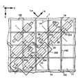
- FIG. 1 is a schematic plan view of a pixel circuit of a solid-state imaging device according to a first embodiment of the present disclosure
- FIG. 2 is a schematic cross-sectional view of a solid-state imaging device including the pixel circuit shown in FIG. 1
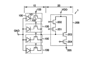
- FIG. 3 is a circuit diagram including pixels and pixel circuits of the solid-state imaging device shown in FIGS. 1 and 2
- FIG. FIG. 4 is a circuit diagram corresponding to FIG. 3 of a solid-state imaging device according to a second embodiment of the present disclosure
- 5 is a schematic plan view corresponding to FIG. 1 of the pixel circuit of the solid-state imaging device shown in FIG. 4
- FIG. FIG. 11 is a schematic cross-sectional view of main parts corresponding to FIG.
- FIG. 11 is a schematic plan view corresponding to FIG. 1 of a pixel circuit of a solid-state imaging device according to a fourth embodiment of the present disclosure
- FIG. 11 is a schematic plan view corresponding to FIG. 1 of a pixel circuit of a solid-state imaging device according to a fifth embodiment of the present disclosure
- FIG. 11 is a schematic cross-sectional view of main parts corresponding to FIG. 2 showing pixels and pixel circuits of a solid-state imaging device according to a sixth embodiment of the present disclosure
- FIG. 21 is a schematic cross-sectional view of a capacitor mounted on a solid-state imaging device according to a seventh embodiment of the present disclosure
- FIG. 11 is a schematic plan view corresponding to FIG. 1 of a pixel circuit of a solid-state imaging device according to a fourth embodiment of the present disclosure
- FIG. 11 is a schematic plan view corresponding to FIG. 1 of a pixel circuit of a solid-state imaging device according to a fifth embodiment of the present disclosure
- FIG. 11 is
- FIG. 20 is a schematic cross-sectional view of a resistor mounted on a solid-state imaging device according to an eighth embodiment of the present disclosure
- FIG. 20 is a schematic cross-sectional view of a memory element mounted on a solid-state imaging device according to a ninth embodiment of the present disclosure
- 1 is a block diagram showing an example of a schematic configuration of a vehicle control system, which is a first application example according to an embodiment of the present disclosure
- FIG. FIG. 4 is an explanatory diagram showing an example of installation positions of an outside information detection unit and an imaging unit
- FIG. 10 is a diagram showing an example of a schematic configuration of an endoscopic surgery system, which is a second application example according to the embodiment of the present disclosure
- 3 is a block diagram showing an example of functional configurations of a camera head and a CCU;
- First Embodiment A first embodiment describes an example in which the present technology is applied to a solid-state imaging device. 2.
- Second Embodiment A second embodiment describes an example in which a plurality of amplification transistors are arranged in one pixel circuit in the solid-state imaging device according to the first embodiment.
- Third Embodiment A third embodiment describes an example in which the bonding method between the first semiconductor layer and the second semiconductor layer is changed in the solid-state imaging device according to the first embodiment.
- Fourth Embodiment A fourth embodiment describes an example in which the planar shape of the pixel circuit is changed in the solid-state imaging device according to the first embodiment. 5.
- Fifth Embodiment A fifth embodiment describes a modification of the arrangement layout of the transistors of the pixel circuit in the solid-state imaging device according to the first embodiment. 6.
- Sixth Embodiment A sixth embodiment describes an example in which the crystal orientation of the second semiconductor layer in which the pixel circuits are arranged is changed in the solid-state imaging device according to the third embodiment. 7.
- Seventh Embodiment A seventh embodiment describes an example in which a capacitor is arranged in the second semiconductor layer in the solid-state imaging device according to the first embodiment.
- Eighth Embodiment An eighth embodiment describes an example in which a resistor is provided in the second semiconductor layer in the solid-state imaging device according to the first embodiment. 9.
- Ninth Embodiment A ninth embodiment describes an example in which a memory element is arranged in the second semiconductor layer in the solid-state imaging device according to the first embodiment. 10.
- Example of Application to Moving Body An example in which the present technology is applied to a vehicle control system, which is an example of a moving body control system, will be described.
- Application Example to Endoscopic Surgery System An example in which the present technology is applied to an endoscopic surgery system will be described. 12.
- FIG. 1 A solid-state imaging device 1 according to a first embodiment of the present disclosure will be described with reference to FIGS. 1 to 3.
- FIG. 1 A solid-state imaging device 1 according to a first embodiment of the present disclosure will be described with reference to FIGS. 1 to 3.
- FIG. 1 A solid-state imaging device 1 according to a first embodiment of the present disclosure will be described with reference to FIGS. 1 to 3.
- FIG. 1 A solid-state imaging device 1 according to a first embodiment of the present disclosure will be described with reference to FIGS. 1 to 3.
- the arrow X direction shown as appropriate indicates one plane direction of the solid-state imaging device 1 placed on a plane for the sake of convenience.
- the arrow Y direction indicates another planar direction perpendicular to the arrow X direction.
- the arrow Z direction indicates an upward direction orthogonal to the arrow X direction and the arrow Y direction. That is, the arrow X direction, the arrow Y direction, and the arrow Z direction exactly match the X-axis direction, the Y-axis direction, and the Z-axis direction of the three-dimensional coordinate system, respectively. It should be noted that each of these directions is shown to aid understanding of the description and is not intended to limit the direction of the present technology.
- FIG. 1 A Circuit Configuration of Pixel 100 and Pixel Circuit 200 of Solid-State Imaging Device 1
- FIG. 1 One pixel 100 is composed of a series circuit of a photoelectric conversion element (photodiode) 101 and a transfer transistor 102 .
- the photoelectric conversion element 101 has an anode terminal connected to the reference potential GND and a cathode terminal connected to one terminal of the transfer transistor 102 .
- the photoelectric conversion element 101 converts light incident from outside the solid-state imaging device 1 into an electric signal.
- the other terminal of the transfer transistor 102 is connected to the pixel circuit 200 .
- a control terminal of the transfer transistor 102 is connected to the horizontal signal line 103 .
- the pixel circuit 200 includes a floating diffusion (FD) conversion gain switching transistor 201 , a reset transistor 202 , an amplification transistor 203 and a selection transistor 204 .
- the other terminal of the transfer transistor 102 is connected to one terminal of the FD conversion gain switching transistor 201 and the control terminal of the amplification transistor 203 .
- the other terminal of the FD conversion gain switching transistor 201 is connected to one terminal of the reset transistor 202 .
- the other terminal of the reset transistor 202 is connected to the power supply potential VDD.
- One terminal of the amplification transistor 203 is connected to one terminal of the selection transistor 204 .
- the other terminal of the amplification transistor 203 is connected to the power supply potential VDD.
- the other terminal of the selection transistor 204 is connected to the vertical signal line 205 .
- one pixel circuit 200 is arranged for four pixels 100 .
- FIG. 2 shows an example of the longitudinal section configuration of the solid-state imaging device 1 .
- the solid-state imaging device 1 is configured as a back-illuminated image sensor here.
- the solid-state imaging device 1 is constructed by sequentially stacking a first substrate 10, a second substrate 20, and a third substrate 30. . That is, the second substrate 20 is laminated on the first substrate 10 and the second substrate 20 is joined to the first substrate 10 .
- a third base 30 is laminated on the second base 20 , and the third base 30 is joined to the second base 20 .
- the first substrate 10 includes a first semiconductor layer 11 and a first wiring layer 12 arranged on the second substrate 20 side of the first semiconductor layer 11 .
- the first semiconductor layer 11 is made of single crystal silicon (Si).
- a pixel 100 is formed in the first semiconductor layer 11 .
- the photoelectric conversion element 101 of the pixel 100 includes an n-type semiconductor region and a p-type semiconductor region, and is composed of a pn junction between the two.
- a light-receiving lens 13 is disposed on the light incident side of the photoelectric conversion element 101 with a charge fixing film and an insulating film (not shown) interposed therebetween.
- a light receiving lens 13 is provided for each pixel 100 .
- the light-receiving lens 13 can condense light incident on the photoelectric conversion element 101 .
- the light incident side is the side opposite to the second substrate 20 side of the first semiconductor layer 11 .
- the transfer transistor 102 of the pixel 100 is formed on the surface portion of the first semiconductor layer 11 on the second substrate 20 side.
- the transfer transistor 102 is formed by an n-channel insulated gate field effect transistor (IGFET).
- the transfer transistor 102 includes a pair of main electrodes (terminals) serving as a source region and a drain region, a channel forming region, a gate insulating film, and a gate electrode (control terminal).
- the IGFET includes a metal/oxide semiconductor field effect transistor (MOSFET) and a metal/insulator/semiconductor field effect transistor (MISFET). contains at least
- a pixel isolation region 14 is arranged between adjacent pixels 100 .
- the pixel isolation region 14 optically and electrically isolates adjacent pixels 100 from each other.
- the arrangement layout of the pixels 100 and the arrangement layout of the pixel isolation regions 14 will be described later in detail together with the arrangement layout of the amplification transistors 203 and the like that construct the pixel circuit 200 .
- the first wiring layer 12 includes wiring 121 , multilayer wiring 122 , first terminals 123 , and insulators 124 .
- One end of the wiring 121 is connected to the transfer transistor 102 and the other end of the wiring 121 is connected to the multilayer wiring 122 .
- the wiring 121 is configured as a through wiring that penetrates the first wiring layer 12 in the thickness direction, and is formed of a wiring material such as dungsten (W).
- W dungsten
- the multilayer wiring 122 has a three-layer wiring structure. Wiring in each layer of the multilayer wiring 122 is connected through a connection hole.
- the multilayer wiring 122 is made of wiring material such as aluminum (Al).
- the first terminal 123 is connected to the multilayer wiring 122 , and the other end of the first terminal 123 is exposed from the surface of the first wiring layer 12 on the side of the second substrate 20 .
- the first terminal 123 is made of copper (Cu), for example.
- the insulator 124 is formed by embedding the wiring 121, the multilayer wiring 122, and the first terminal 123 respectively.
- the insulator 124 is actually formed by laminating a plurality of insulating films.
- the insulator 124 is formed of a silicon oxide film (SiO), a silicon nitride film (SiN), or a combination of both.
- the second substrate 20 includes a second semiconductor layer 21 and a second wiring layer 22 disposed on the first substrate 10 side of the second semiconductor layer 21 .
- the second semiconductor layer 21 is made of single crystal silicon.
- a pixel circuit 200 is formed in the second semiconductor layer 21 . That is, the second semiconductor layer 21 includes an FD conversion gain switching transistor 201, a reset transistor 202, an amplification transistor 203, and a selection transistor 204 (see FIG. 3).
- Each of the FD conversion gain switching transistor 201, the reset transistor 202, the amplification transistor 203, and the selection transistor 204 that construct the pixel circuit 200 corresponds to the "first transistor" according to the present technology.
- the pixel circuit 200 is arranged on the main surface portion of the second semiconductor layer 21 on the first substrate 10 side.
- the main surface portion is used to mean a main surface portion on which transistors, capacitors, resistors, and the like are formed.
- the reset transistor 202 is arranged on the main surface portion of the second semiconductor layer 21 within the region surrounded by the isolation region 28 .
- a trench-structure element isolation region 28 is used here to improve the degree of integration.
- the reset transistor 202 has a pair of main electrodes 23 , a channel forming region, a gate insulating film 25 and a gate electrode 26 .
- a pair of main electrodes 23 are a source region and a drain region, and are formed of an n-type semiconductor region.
- a channel forming region is formed by the second semiconductor layer 21 between the pair of main electrodes 23 .
- the gate insulating film 25 is arranged along the channel forming region and is formed of, for example, a silicon oxide film, a silicon nitride film, or a laminated film thereof.
- the gate electrode 26 is arranged along the gate insulating film 25 and made of polycrystalline silicon, for example.
- the reset transistor 202 like the transfer transistor 102, is composed of an n-channel IGFET.
- the gate length direction of the first transistor according to the present technology is the direction in which carriers flow between the pair of main electrodes 23 and is the same direction as the channel length direction.
- the selection transistor 204 is arranged on the main surface of the second semiconductor layer 21 within a region surrounded by the isolation region 28 .
- the select transistor 204 includes a pair of main electrodes 23 , a channel forming region, a gate insulating film 25 and a gate electrode 26 .
- the selection transistor 204 is composed of an n-channel IGFET.
- the FD conversion gain switching transistor 201 is arranged on the main surface of the second semiconductor layer 21 in a region surrounded by the element isolation region 28, like the reset transistor 202. is provided (see FIG. 1).
- the FD conversion gain switching transistor 201 has a pair of main electrodes 23 , a channel forming region, a gate insulating film 25 and a gate electrode 26 .
- the FD conversion gain switching transistor 201 is composed of an n-channel IGFET.
- the amplification transistor 203 is arranged on the main surface portion of the second semiconductor layer 21 within the region surrounded by the isolation region 28 .
- the amplification transistor 203 includes a pair of main electrodes 23 , a channel forming region, a gate insulating film 25 and a gate electrode 26 .
- the amplification transistor 203 is composed of an n-channel IGFET.
- the amplification transistor 203 has a fin structure. In the fin-type structure, both ends of the gate electrode 26 (and the gate insulating film 25) in the gate width direction extend from the main surface of the second semiconductor layer 21 in the depth direction, thereby expanding the gate width dimension in the depth direction. Structure. When the fin structure is adopted, the amount of current flowing through the amplification transistor 203 can be increased.
- the second wiring layer 22 includes wiring 221 , multilayer wiring 222 , second terminals 223 , and insulators 224 .
- One end of the wiring 221 is connected to the amplification transistor 203 and the other end of the wiring 221 is connected to the multilayer wiring 222 .
- the wiring 221 is configured as a through wiring that penetrates the second wiring layer 22 in the thickness direction.
- the multilayer wiring 222 has a three-layer wiring structure, although the number of layers is not limited.
- One end of the second terminal 223 is connected to the multilayer wiring 222 , and the other end of the second terminal 223 is exposed from the surface of the second wiring layer 22 on the side of the first substrate 10 similarly to the first terminal 123 .
- the second terminal 223 is arranged at a position corresponding to the first terminal 123 and is joined and electrically connected to the first terminal 123 .
- the insulator 224 is formed by embedding the wiring 221 , the multilayer wiring 222 and the second terminal 223 .
- the insulator 224 is made of the same material as the insulator 124 .
- the first terminal 123 of the first base 10 and the second terminal 223 of the second base 20 face each other and are joined together. That is, the first base 10 and the second base 20 are connected by a face-to-face connection structure.
- the third substrate 30 includes a third semiconductor layer 31 and a third wiring layer 32 provided on the third semiconductor layer 31 on the second substrate 20 side.
- the third semiconductor layer 31 is made of single crystal silicon.
- a peripheral circuit 300 that controls the operation of the pixel circuit 200 is arranged in the third semiconductor layer 31 .
- the peripheral circuit 300 includes, for example, an input section, a timing control section, a row driving section, a column signal processing section, an image signal processing section, and an output section.
- Peripheral circuit 300 comprises complementary IGFETs including an n-channel IGFET 301 and a p-channel IGFET 302 .
- a complementary IGFET corresponds to the "second transistor" according to the present technology.
- the n-channel IGFET 301 is arranged on the main surface of the third semiconductor layer 31 within the region surrounded by the isolation region 38 .
- a trench structure is used for the element isolation region 38 in the same manner as the element isolation region 28 .
- the n-channel IGFET 301 includes a pair of main electrodes 33 , a channel forming region, a gate insulating film 35 and a gate electrode 36 .
- a pair of main electrodes 33 are a source region and a drain region, and are formed of an n-type semiconductor region.
- a channel forming region is formed by the third semiconductor layer 31 between the pair of main electrodes 33 .
- the gate insulating film 35 is arranged along the channel forming region and is made of the same material as the gate insulating film 25, for example.
- the gate electrode 36 is arranged along the gate insulating film 35 and is made of the same material as the gate electrode 26, for example.
- the p-channel IGFET 302 includes a pair of main electrodes 34 , a channel forming region, a gate insulating film 35 and a gate electrode 36 .
- a pair of main electrodes 34 are a source region and a drain region, and are formed of a p-type semiconductor region.
- a channel forming region is formed by the third semiconductor layer 31 between the pair of main electrodes 34 .
- the n-channel IGFET 301 is formed in a p-type well region provided on the main surface of the third semiconductor layer 31 .
- a p-channel IGFET 302 is formed in an n-type well region provided on the main surface of the third semiconductor layer 31 .
- the third wiring layer 32 includes wiring 321 , multilayer wiring 322 and insulator 324 .
- One end of the wiring 321 is connected to the complementary IGFET, and the other end of the wiring 321 is connected to the multilayer wiring 322 .
- the wiring 321 is configured as a through wiring that penetrates the third wiring layer 32 in the thickness direction.
- the multilayer wiring 322 has a three-layer wiring structure, although the number of layers is not limited.
- the multi-layered wiring 322 is connected to the multi-layered wiring 222 of the second substrate 20 through through wirings (not shown).
- the insulator 324 is formed by embedding the wiring 321 and the multilayer wiring 322 respectively.
- the insulator 324 is made of the same material as the insulator 124 .
- FIG. 1 shows the arrangement layout and layout of the pixels 100 when the solid-state imaging device 1 is viewed from the light incident side in the direction of the arrow Z (hereinafter simply referred to as “planar view”).
- An example of an arrangement layout of the pixel circuit 200 is shown.
- a plurality of pixels 100 are arranged in a matrix along a surface direction parallel to the surface of the first semiconductor layer 11 of the first substrate 10 . That is, the pixels 100 are arranged at regular intervals in the arrow X direction and the arrow Y direction. Pixel isolation regions 14 are arranged between the pixels 100 adjacent in the arrow X direction and between the pixels 100 adjacent in the arrow Y direction.
- the pixel 100 is formed in a rectangular shape in plan view, more specifically in a square shape.
- the FD conversion gain switching transistor 201 and the reset transistor 202 are arranged in a line along the main surface of the second semiconductor layer 21 with their gate length directions aligned.
- the direction of gate length is the direction of the arrow labeled "Lg”.
- the direction of the gate width is the direction of the arrow labeled "Lw”.
- One main electrode 23 of the FD conversion gain switching transistor 201 is formed integrally with one main electrode 23 of the reset transistor 202 .
- the gate length directions of the FD conversion gain switching transistor 201 and the reset transistor 202 are inclined with respect to the arrangement direction of the pixels 100 (arrow X direction or arrow Y direction).
- the FD conversion gain switching transistor 201 and the reset transistor 202 are arranged so as to match the diagonal direction of the rectangular shape of the pixel 100, that is, with the gate length direction parallel to the diagonal direction.
- the amplification transistor 203 and the selection transistor 204 are arranged in a line along the main surface of the second semiconductor layer 21 with their gate length directions aligned.
- One main electrode 23 of the amplification transistor 203 is formed integrally with one main electrode 23 of the selection transistor 204 .
- the gate length direction of the amplification transistor 203 and selection transistor 204 is inclined with respect to the arrangement direction of the pixels 100 (arrow X direction or arrow Y direction).
- the amplification transistor 203 and the selection transistor 204 are parallel to the FD conversion gain switching transistor 201 and the reset transistor 202 in the gate length direction and separated in the gate width direction.
- one pixel circuit 200 is arranged for four pixels 100 .
- the FD conversion gain switching transistor 201 of one pixel circuit 200 is arranged with the gate length direction aligned with the diagonal direction of one of the four pixels 100 .
- the reset transistor 202 of one pixel circuit 200 is arranged in the diagonal direction of one of the four pixels 100 so as to match the gate length direction.
- the amplifying transistor 203 of one pixel circuit 200 is arranged in the diagonal direction of one of the four pixels 100 so that the gate length direction matches.
- the selection transistor 204 of one pixel circuit 200 is arranged with the gate length direction aligned with the diagonal direction of one pixel 100 out of the four.
- the dimension of one side of one pixel 100 is set to, for example, 0.4 ⁇ m or more and 2.0 ⁇ m or less.
- the gate length dimension of each of the FD conversion gain switching transistor 201, the reset transistor 202, and the selection transistor 204 of the pixel circuit 200 is set to, for example, 150 nm or more and 300 nm or less.
- the gate length dimension of the amplification transistor 203 is longer than the gate length dimension of the reset transistor 202, etc., and is set to, for example, 300 nm or more and 600 nm or less.
- the pixel isolation regions 14 are provided between the pixels 100, and the pixel isolation regions 14 are formed in a grid pattern in plan view. That is, the pixel separation region 14 includes the first separation walls 141 extending in the arrow X direction and arranged at regular intervals in the arrow Y direction, and the first separation walls 141 extending in the arrow Y direction and arranged at regular intervals in the arrow X direction. and a second separation wall 142 that Therefore, the gate length direction of the FD conversion gain switching transistor 201 and the like of the pixel circuit 200 is inclined with respect to the extending direction of the first separation wall 141 or the second separation wall 142 .
- the gate length direction of each of the n-channel IGFET 301 and the p-channel IGFET 302 constructing the peripheral circuit 300 is parallel to the arrangement direction of the pixels 100 .
- the solid-state imaging device 1 includes a first semiconductor layer 11 and a second semiconductor layer 21, as shown in FIG.
- a first semiconductor layer 11 in the first semiconductor layer 11, a plurality of pixels 100 having photoelectric conversion elements 101 are arranged in a matrix along the surface direction.
- the second semiconductor layer 21 is stacked on the first semiconductor layer 11 on the side opposite to the light incident side of the pixel 100 .
- the second semiconductor layer 21 is provided with a first transistor which is electrically connected to the pixels 100 and whose gate length direction is inclined with respect to the arrangement direction of the pixels 100 .
- the first transistors are the FD conversion gain switching transistor 201, the reset transistor 202, the amplification transistor 203, or the selection transistor 204 that construct the pixel circuit 200.
- a pixel 100 is arranged on the first semiconductor layer 11 , and a first transistor is arranged on the second semiconductor layer 21 independently of the pixel 100 . Therefore, even if the pixels 100 are miniaturized and the number of pixels 100 arranged is increased, the area for arranging the first transistors in the second semiconductor layer 21 can be secured.
- the gate length direction of the first transistor is inclined with respect to the arrangement direction of the pixels 100, the gate length dimension of the first transistor can be increased. Therefore, it is possible to effectively suppress or prevent the occurrence of the short-channel effect or the occurrence of noise in the first transistor, thereby improving the electrical characteristics of the first transistor.
- the amplification transistor 203 as the first transistor can effectively suppress or prevent the generation of RTS (Random Telegraph Signal) noise.
- the electrical characteristics of the pixel circuit 200 can be improved.
- the gate length direction of the first transistor is inclined with respect to the arrangement direction of the pixels 100, the gate width dimension of the first transistor can be expanded.
- the gate width dimensions of each of the amplification transistor 203 and the selection transistor 204 can be expanded. Therefore, the mutual conductance (gm) of each of the amplification transistor 203 and the selection transistor 204 can be improved, and thermal noise can be effectively suppressed or prevented. Also, since the mutual conductance is improved, the operating speed of the pixel circuit 200 can be increased.
- the pixels 100 are formed in a rectangular shape in plan view.
- the gate length direction of the first transistor is parallel to the diagonal direction of the pixel 100 in plan view. Therefore, the gate length dimension of the first transistor can be maximized.
- the gate length dimension of the first transistor can be increased by about 1.4 times. Therefore, the electrical characteristics of the first transistor can be further improved.
- the first transistor constructs a pixel circuit 200 connected to the pixel 100, as shown in FIG. That is, as shown in FIG. 2, the pixel 100 is arranged on the first semiconductor layer 11 and the pixel circuit 200 is arranged on the second semiconductor layer 21 . Therefore, the pixels 100 can be miniaturized and the number of pixels 100 arranged can be increased independently of the arrangement area of the pixel circuits 200 .
- the gate length dimension of the amplification transistor 203 as the first transistor is longer than the gate length dimension of the selection transistor 204 or the reset transistor 202. Therefore, in the amplification transistor 203, the generation of RTS noise can be suppressed or prevented more effectively, so that the electrical characteristics can be further improved.
- the solid-state imaging device 1 includes a first terminal 123 and a second terminal 223, as shown in FIG.
- the first terminal 123 is arranged on the second semiconductor layer 21 side of the first semiconductor layer 11 and electrically connected to the pixel 100 via the first wiring layer 12 .
- the second terminal 223 is arranged on the first semiconductor layer 11 side of the second semiconductor layer 21 , electrically connected to the first transistor via the second wiring layer 22 , and joined to the first terminal 123 .
- the first substrate 10 having the first semiconductor layer 11 and the second substrate 20 having the second semiconductor layer 21 are connected by a face-to-face connection structure.
- the second wiring layer 222 is arranged in the connection path between the second terminal 223 and the first transistor in the connection path between the pixel 100 and the first transistor. Therefore, since the wiring can be routed in the second wiring layer 22, the arrangement position of the first transistor can be freely laid out.
- the solid-state imaging device 1 also includes a third semiconductor layer 31 as shown in FIG.
- the third semiconductor layer 31 is stacked on the side of the second semiconductor layer 21 opposite to the first semiconductor layer 11 .
- the third semiconductor layer 31 has a second transistor, which builds a peripheral circuit 300 that controls the pixel circuit 200 .
- the second transistor is, for example, a complementary IGFET. That is, the pixel 100 is arranged on the first semiconductor layer 11 , the pixel circuit 200 is arranged on the second semiconductor layer 21 , and the peripheral circuit 300 is arranged on the third semiconductor layer 31 . Therefore, the pixels 100 can be mainly arranged in the first semiconductor layer 11, so that the number of pixels 100 arranged can be increased.
- the gate length direction of the second transistor shown in FIG. 2 is parallel to the arrangement direction of the pixels 100 .
- the gate length direction of the first transistor constructing the pixel circuit 200 is inclined with respect to the gate length direction of the second transistor. Therefore, the electrical characteristics of the first transistor can be optimized independently of the second transistor.
- Second Embodiment> A solid-state imaging device 2 according to a second embodiment of the present disclosure will be described with reference to FIGS. 4 and 5.
- FIG. 4 shows an example of the circuit configuration of the pixels 100 and the pixel circuits 200 that construct the solid-state imaging device 2 .
- the pixel circuit 200 includes an FD conversion gain switching transistor 201 , a reset transistor 202 , two amplification transistors 203 and a selection transistor 204 .
- two amplification transistors 203 are arranged in one pixel circuit 200 .
- the two amplification transistors 203 are electrically connected in parallel.
- FIG. 5 shows an example of the arrangement layout of the pixels 100 and the arrangement layout of the pixel circuits 200 of the solid-state imaging device 2 in plan view.
- the FD conversion gain switching transistor 201 and the reset transistor 202 are arranged in a line along the main surface of the second semiconductor layer 21 with their gate length directions aligned.
- One main electrode 23 of the FD conversion gain switching transistor 201 is formed integrally with one main electrode 23 of the reset transistor 202 .
- the gate length directions of the FD conversion gain switching transistor 201 and the reset transistor 202 are inclined with respect to the arrangement direction of the pixels 100 .
- the FD conversion gain switching transistor 201 and the reset transistor 202 are arranged such that the gate length direction matches the diagonal direction of the rectangular shape of the pixel 100. are arranged.
- the selection transistor 204 is arranged on the extension of the gate length direction of the FD conversion gain switching transistor 201 and the reset transistor 202 so as to match the gate length direction.
- the two amplification transistors 203 are arranged in a line along the main surface of the second semiconductor layer 21 with their gate length directions aligned.
- One main electrode 23 of each of the two amplification transistors 203 is integrally formed.
- the gate length direction of the two amplification transistors 203 is inclined with respect to the arrangement direction of the pixels 100 .
- the two amplification transistors 203 are parallel to the FD conversion gain switching transistor 201, the reset transistor 202, and the selection transistor 204 in the gate length direction and separated in the gate width direction.
- Components other than the pixel circuit 200 are the same as those of the solid-state imaging device 1 according to the first embodiment.
- a plurality of amplification transistors 203 are electrically connected in parallel to one pixel circuit 200, as shown in FIGS.
- two amplification transistors 203 are electrically connected in parallel. Therefore, in the amplification transistor 203, the generation of RTS noise can be suppressed or prevented more effectively, so that the electrical characteristics can be further improved.
- FIG. 6 shows an example of a vertical cross-sectional configuration of a main part showing the pixel 100 and the pixel circuit 200 of the solid-state imaging device 3.
- the solid-state imaging device 3 according to the third embodiment includes a first base 10, a second base 20, and a third base (not shown) in a side view. 30 are sequentially laminated.
- the second substrate 20 has the second semiconductor layer 21 on the first substrate 10 side and the second wiring layer 22 on the third substrate 30 side.
- the main surface of the second semiconductor layer 21 faces the third substrate 30, and the main surface of the second semiconductor layer 21 is configured with an amplifying transistor 203 and the like that construct the pixel circuit 200 (see FIG. 3 or 4).
- the pixels 100 and pixel circuits 200 are electrically connected to each other using through-wirings 125 .
- One end of the through wire 125 is connected to the transfer transistor 102 of the pixel 100 .
- the other end of the through wire 125 passes through the second semiconductor layer 21 in the thickness direction and is connected to the second wiring layer 22 .
- the second wiring layer 22 is connected to the amplification transistor 203 and the FD conversion gain switching transistor 201 (not shown). That is, the first base 10 and the second base 20 are connected by a face-to-back connection structure.
- connection structure Components other than the connection structure are the same as those of the solid-state imaging device 1 according to the first embodiment.
- the first substrate 10 having the first semiconductor layer 11 and the second substrate having the second semiconductor layer 21 are connected by a face-to-back connection structure.
- the pixels 100 and the pixel circuits 200 are connected by through-wirings 125, respectively. Therefore, the length of the signal path connecting the pixel 100 and the pixel circuit 200 is shorter than that of the solid-state imaging device 1 according to the first embodiment, for example. Therefore, the signal-to-noise ratio (SN ratio) can be reduced.
- FIG. 7 shows an example of the array layout of the pixels 100 and the array layout of the pixel circuits 200 of the solid-state imaging device 4 .
- the pixel 100 in plan view, is formed in a rectangular shape in which the side parallel to the arrow Y direction is longer than the side parallel to the arrow X direction.
- the first transistors such as the amplifying transistor 203 that constitute the pixel circuit 200 are arranged so that the gate length direction is parallel to the diagonal direction of the pixel 100 .
- FIG. 8 shows an example of an array layout of the pixels 100 and an array layout of the pixel circuits 200 of the solid-state imaging device 5.
- a solid-state imaging device 5 according to the fifth embodiment includes a plurality of pixel regions in plan view.
- the solid-state imaging device 5 has two first pixel regions 15 and a second pixel region 16 for simplicity of explanation.
- the first transistors are arranged as in the solid-state imaging device 1 according to the first embodiment. That is, the FD conversion gain switching transistor 201, the reset transistor 202, the amplification transistor 203, and the selection transistor 204, which constitute the pixel circuit 200, are arranged with the gate length direction inclined with respect to the arrangement direction of the pixels 100.
- FIG. The gate length direction of the amplification transistor 203 and the like is parallel to the diagonal direction of the pixel 100 .
- the gate length direction of the amplifying transistor 203 and the like is set at an angle ⁇ 1 in the counterclockwise direction with reference to a boundary line CC that is virtually set at the boundary between the first pixel region 15 and the second pixel region 16 .
- the angle ⁇ 1 here is 45 degrees.
- the FD conversion gain switching transistor 201, the reset transistor 202, the amplification transistor 203, and the selection transistor 204, which constitute the pixel circuit 200, are arranged by tilting the gate length direction with respect to the arrangement direction of the pixels 100. ing.
- the gate length direction of the amplification transistor 203 and the like is parallel to the diagonal direction of the pixel 100 .
- the gate length direction of the amplifying transistor 203 and the like is set clockwise at an angle ⁇ 2 with reference to the boundary line CC.
- the angle ⁇ 2 here is 45 degrees.
- the gate length direction of the first pixel region 15 is set to be orthogonal to the gate length direction of the second pixel region 16 .
- the gate length direction of the second pixel region 16 is parallel to the gate width direction of the first pixel region 15 .
- FIG. 9 shows an example of a vertical cross-sectional configuration of a main part showing the pixel 100 and the pixel circuit 200 of the solid-state imaging device 6. As shown in FIG. Here, a modification of the solid-state imaging device 3 according to the third embodiment will be described.
- a solid-state imaging device 6 according to the sixth embodiment includes a second semiconductor layer 21N instead of the second semiconductor layer 21 of the second substrate 20 of the solid-state imaging device 3 according to the third embodiment.
- the second semiconductor layer 21N is diced from a semiconductor wafer (single-crystal silicon substrate) having a 0 (zero) degree notch, which is used in the manufacturing process of the solid-state imaging device 6 .
- the diced side surface of the second semiconductor layer 21N is the ⁇ 110> crystal plane.
- the amplification transistor 203 arranged on the main surface of the second semiconductor layer 21N employs a fin structure as described above, and the gate length direction is inclined at 45 degrees with respect to the arrangement direction of the pixels 100. FIG. Therefore, the side walls of the channel forming region (second semiconductor layer 21N) of the amplifying transistor 203 are set to the ⁇ 100> crystal plane.
- the solid-state imaging device 6 also includes a second semiconductor layer 21N diced from a semiconductor wafer having a 0-degree notch.
- a second semiconductor layer 21N diced from a semiconductor wafer having a 0-degree notch.
- an amplifying transistor 203 having a fin-type structure with a gate length direction parallel to the arrangement direction of the pixels 100 is arranged. Therefore, the side surface of the channel forming region of the amplifying transistor 203 becomes the ⁇ 100> crystal plane.
- the ⁇ 100> crystal plane has a lower interface level that worsens noise than the ⁇ 110> crystal plane. Therefore, noise in the amplification transistor 203 can be effectively suppressed or prevented. Note that even when the second semiconductor layer 21 is replaced with the second semiconductor layer 21N in the solid-state imaging device 1 according to the first embodiment, the effects obtained by the solid-state imaging device 6 according to the sixth embodiment are the same. It is possible to obtain the effects of
- FIG. 10 shows an example of a vertical cross-sectional configuration of the capacitor 206 mounted on the second substrate 20 of the solid-state imaging device 7.
- the solid-state imaging device 7 includes a capacitor (capacitive element) 206 in a region inside or outside the pixel circuit 200 in the second semiconductor layer 21 of the second substrate 20 .
- the capacitor 206 includes a second semiconductor layer 21 as a second electrode, a dielectric 25A provided on the second semiconductor layer 21, and a metal 26A provided on the dielectric 25A as a first electrode. It has That is, the capacitor 206 is configured as a metal/dielectric/semiconductor type capacitor.
- the second semiconductor layer 21 of the capacitor 206 is made of single crystal silicon.
- the dielectric 25A is made of the same material as the gate insulating film 25 (see FIG. 2) of the selection transistor 204, etc. that constructs the pixel circuit 200, for example.
- the metal body 26A is made of the same material as the gate electrode 26 of the selection transistor 204, for example. If the dielectric 25A is made of silicon oxide, the capacitor 206 is configured as a MOS (Metal Oxide Semiconductor) type capacitor. If the dielectric 25A is made of an insulator other than silicon oxide, such as silicon nitride, the capacitor 206 is configured as a MIS (Metal Insulator Semiconductor) type capacitor.
- the capacitor 206 is arranged in the second semiconductor layer 21 with the center line Lc along the surface direction of the metal body 26A parallel to the gate length direction of the selection transistor 204, for example.
- the solid-state imaging device 7 also includes a capacitor 206 in the second semiconductor layer 21 of the second substrate 20, as shown in FIG. Therefore, the second semiconductor layer 21 can be effectively used.
- a circuit including the capacitor 206 can be mounted on the second semiconductor layer 21 .
- the capacitor 206 is arranged in the second semiconductor layer 21 with the center line Lc of the metal body 26A as the first electrode parallel to the gate length direction of the selection transistor 204 and the like. Therefore, the capacitor 206 can be elongated in the center line Lc and the dimension in the direction perpendicular to the center line Lc to increase the capacitor area, so that the capacitance value of the capacitor 206 can be increased.
- FIG. 11 shows an example of a vertical cross-sectional configuration of the resistor 207 mounted on the second substrate 20 of the solid-state imaging device 8.
- the solid-state imaging device 8 includes a resistor (resistive element) 207 in a region inside or outside the pixel circuit 200 in the second semiconductor layer 21 of the second substrate 20 .
- the resistor 207 is formed by a semiconductor region (diffusion layer) 23A provided on the main surface portion of the second semiconductor layer 21 . That is, resistor 207 is a diffusion layer resistor.
- the semiconductor region 23A is formed with the same structure as the main electrode 23 such as the selection transistor 204 that constructs the pixel circuit 200, for example.
- the semiconductor region 23A is an n-type semiconductor region.
- the semiconductor region 23A may be formed of a p-type semiconductor region, or a p-type well region or an n-type well region (not shown).
- the resistor 207 may be made of the same material as the gate electrode 26 of the selection transistor 204, for example. If the gate electrode 26 is made of, for example, polycrystalline silicon, the resistor 207 will be a polysilicon resistor.
- the resistor 207 is arranged in the second semiconductor layer 21 with the resistance length direction Lr parallel to the gate length direction of the selection transistor 204, for example.
- the solid-state imaging device 8 also includes a resistor 207 on the second semiconductor layer 21 of the second substrate 20, as shown in FIG. Therefore, the second semiconductor layer 21 can be effectively used.
- a circuit including the resistor 207 can be mounted on the second semiconductor layer 21 .
- the resistor 207 is arranged in the second semiconductor layer 21 with the resistance length direction Lr parallel to the gate length direction of the selection transistor 204 and the like. Therefore, the resistance length dimension of the resistor 207 can be lengthened, so that the resistance value of the resistor 207 can be increased.
- the solid-state imaging device 8 according to the eighth embodiment may be combined with the solid-state imaging device 7 according to the seventh embodiment, and the second semiconductor layer 21 may be provided with the resistor 207 and the capacitor 206 .
- FIG. 12 shows an example of a vertical cross-sectional configuration of the memory element 208 mounted on the second substrate 20 of the solid-state imaging device 9.
- the solid-state imaging device 9 includes a memory element 208 in a region inside or outside the pixel circuit 200 on the second semiconductor layer 21 of the second substrate 20 .
- the memory element 208 is a memory cell that employs a one-transistor structure of ferroelectric random access memory (FeRAM). Also, although only one memory element 208 is shown, a plurality of memory elements 208 are actually arranged in a matrix.
- FeRAM ferroelectric random access memory
- the memory element 208 includes a pair of main electrodes 23B, which are source and drain regions, a channel forming region, a ferroelectric 25B, and a gate electrode 26B.
- the main electrode 23B is formed with the same structure as the main electrode 23 such as the selection transistor 204 constructing the pixel circuit 200, for example. That is, the main electrode 23B is an n-type semiconductor region. Although the reference numerals are omitted, sidewall spacers are formed on the sidewalls of the gate electrode 26B. Using sidewall spacers, the main electrode 23B is formed in an LDD (Lightly Doped Drain) structure.
- a channel forming region is formed by the second semiconductor layer 21 between the pair of main electrodes 23B.
- a ferroelectric 25B is formed on the channel forming region.
- the ferroelectric 25B uses, for example, a high-kappa-key (High-k) insulator having a higher dielectric constant than silicon dioxide.
- the ferroelectric 25B is made of zirconium hafnium oxide (HfZrO), zirconium oxide (ZrO), hafnium oxide (HfO), or the like.
- a gate electrode 26B is formed on the ferroelectric 25B.
- the gate electrode 26B is made of the same material as the gate electrode 26 of the selection transistor 204, for example.
- the memory element 208 is arranged in the second semiconductor layer 21 such that the gate length direction of the memory element 208 is parallel to the gate length direction of the selection transistor 204 and the like.
- the solid-state imaging device 9 also includes a memory element 208 on the second semiconductor layer 21 of the second substrate 20, as shown in FIG. Therefore, the second semiconductor layer 21 can be effectively used.
- a circuit including a ferroelectric memory can be mounted on the second semiconductor layer 21 .
- the gate length direction of the memory element 208 is parallel to the gate length direction of the select transistor 204 and the like (see FIG. 1 ) forming the pixel circuit 200 , and the second semiconductor layer 21 has a memory cell.
- An element 208 is provided. Therefore, in the memory element 208, the short channel effect and noise can be effectively suppressed or prevented, so that electrical reliability can be improved. In addition, since the dimension in the gate width direction can be extended in the memory element 208, mutual conductance can be improved.
- the solid-state imaging device 9 according to the ninth embodiment is combined with the solid-state imaging device 7 according to the seventh embodiment or the solid-state imaging device 8 according to the eighth embodiment, and the memory element is formed in the second semiconductor layer 21 .
- 208 and capacitor 206 or resistor 207 may be provided.
- the solid-state imaging device 9 according to the ninth embodiment is combined with the solid-state imaging device 7 according to the seventh embodiment and the solid-state imaging device 8 according to the eighth embodiment, and the memory element is formed in the second semiconductor layer 21 .
- a capacitor 206 and a resistor 207 may be provided.
- the technology (the present technology) according to the present disclosure can be applied to various products.
- the technology according to the present disclosure can be realized as a device mounted on any type of moving body such as automobiles, electric vehicles, hybrid electric vehicles, motorcycles, bicycles, personal mobility, airplanes, drones, ships, and robots. may
- FIG. 13 is a block diagram showing a schematic configuration example of a vehicle control system, which is an example of a mobile control system to which the technology according to the present disclosure can be applied.
- a vehicle control system 12000 includes a plurality of electronic control units connected via a communication network 12001.
- the vehicle control system 12000 includes a drive system control unit 12010, a body system control unit 12020, an exterior information detection unit 12030, an interior information detection unit 12040, and an integrated control unit 12050.
- a microcomputer 12051, an audio/image output unit 12052, and an in-vehicle network I/F (Interface) 12053 are illustrated.
- the drive system control unit 12010 controls the operation of devices related to the drive system of the vehicle according to various programs.
- the driving system control unit 12010 includes a driving force generator for generating driving force of the vehicle such as an internal combustion engine or a driving motor, a driving force transmission mechanism for transmitting the driving force to the wheels, and a steering angle of the vehicle. It functions as a control device such as a steering mechanism to adjust and a brake device to generate braking force of the vehicle.
- the body system control unit 12020 controls the operation of various devices equipped on the vehicle body according to various programs.
- the body system control unit 12020 functions as a keyless entry system, a smart key system, a power window device, or a control device for various lamps such as headlamps, back lamps, brake lamps, winkers or fog lamps.
- the body system control unit 12020 can receive radio waves transmitted from a portable device that substitutes for a key or signals from various switches.
- the body system control unit 12020 receives the input of these radio waves or signals and controls the door lock device, power window device, lamps, etc. of the vehicle.
- the vehicle exterior information detection unit 12030 detects information outside the vehicle in which the vehicle control system 12000 is installed.
- the vehicle exterior information detection unit 12030 is connected with an imaging section 12031 .
- the vehicle exterior information detection unit 12030 causes the imaging unit 12031 to capture an image of the exterior of the vehicle, and receives the captured image.
- the vehicle exterior information detection unit 12030 may perform object detection processing or distance detection processing such as people, vehicles, obstacles, signs, or characters on the road surface based on the received image.
- the imaging unit 12031 is an optical sensor that receives light and outputs an electrical signal according to the amount of received light.
- the imaging unit 12031 can output the electric signal as an image, and can also output it as distance measurement information.
- the light received by the imaging unit 12031 may be visible light or non-visible light such as infrared rays.
- the in-vehicle information detection unit 12040 detects in-vehicle information.
- the in-vehicle information detection unit 12040 is connected to, for example, a driver state detection section 12041 that detects the state of the driver.
- the driver state detection unit 12041 includes, for example, a camera that captures an image of the driver, and the in-vehicle information detection unit 12040 detects the degree of fatigue or concentration of the driver based on the detection information input from the driver state detection unit 12041. It may be calculated, or it may be determined whether the driver is dozing off.
- the microcomputer 12051 calculates control target values for the driving force generator, the steering mechanism, or the braking device based on the information inside and outside the vehicle acquired by the vehicle exterior information detection unit 12030 or the vehicle interior information detection unit 12040, and controls the drive system control unit.
- a control command can be output to 12010 .
- the microcomputer 12051 realizes the functions of ADAS (Advanced Driver Assistance System) including collision avoidance or shock mitigation of vehicles, follow-up driving based on inter-vehicle distance, vehicle speed maintenance driving, vehicle collision warning, vehicle lane deviation warning, etc. Cooperative control can be performed for the purpose of ADAS (Advanced Driver Assistance System) including collision avoidance or shock mitigation of vehicles, follow-up driving based on inter-vehicle distance, vehicle speed maintenance driving, vehicle collision warning, vehicle lane deviation warning, etc. Cooperative control can be performed for the purpose of ADAS (Advanced Driver Assistance System) including collision avoidance or shock mitigation of vehicles, follow-up driving based on inter-vehicle distance, vehicle speed maintenance driving
- the microcomputer 12051 controls the driving force generator, the steering mechanism, the braking device, etc. based on the information about the vehicle surroundings acquired by the vehicle exterior information detection unit 12030 or the vehicle interior information detection unit 12040, so that the driver's Cooperative control can be performed for the purpose of autonomous driving, etc., in which vehicles autonomously travel without depending on operation.
- the microcomputer 12051 can output a control command to the body system control unit 12030 based on the information outside the vehicle acquired by the information detection unit 12030 outside the vehicle.
- the microcomputer 12051 controls the headlamps according to the position of the preceding vehicle or the oncoming vehicle detected by the vehicle exterior information detection unit 12030, and performs cooperative control aimed at anti-glare such as switching from high beam to low beam. It can be carried out.
- the audio/image output unit 12052 transmits at least one of audio and/or image output signals to an output device capable of visually or audibly notifying the passengers of the vehicle or the outside of the vehicle.
- an audio speaker 12061, a display unit 12062, and an instrument panel 12063 are illustrated as output devices.
- the display unit 12062 may include at least one of an on-board display and a head-up display, for example.
- FIG. 14 is a diagram showing an example of the installation position of the imaging unit 12031.
- the imaging unit 12031 has imaging units 12101, 12102, 12103, 12104, and 12105.
- the imaging units 12101, 12102, 12103, 12104, and 12105 are provided at positions such as the front nose, side mirrors, rear bumper, back door, and windshield of the vehicle 12100, for example.
- An image pickup unit 12101 provided in the front nose and an image pickup unit 12105 provided above the windshield in the passenger compartment mainly acquire images in front of the vehicle 12100 .
- Imaging units 12102 and 12103 provided in the side mirrors mainly acquire side images of the vehicle 12100 .
- An imaging unit 12104 provided in the rear bumper or back door mainly acquires an image behind the vehicle 12100 .
- the imaging unit 12105 provided above the windshield in the passenger compartment is mainly used for detecting preceding vehicles, pedestrians, obstacles, traffic lights, traffic signs, lanes, and the like.
- FIG. 14 shows an example of the imaging range of the imaging units 12101 to 12104.
- the imaging range 12111 indicates the imaging range of the imaging unit 12101 provided in the front nose
- the imaging ranges 12112 and 12113 indicate the imaging ranges of the imaging units 12102 and 12103 provided in the side mirrors, respectively
- the imaging range 12114 The imaging range of an imaging unit 12104 provided on the rear bumper or back door is shown. For example, by superimposing the image data captured by the imaging units 12101 to 12104, a bird's-eye view image of the vehicle 12100 viewed from above can be obtained.
- At least one of the imaging units 12101 to 12104 may have a function of acquiring distance information.
- at least one of the imaging units 12101 to 12104 may be a stereo camera composed of a plurality of imaging elements, or may be an imaging element having pixels for phase difference detection.
- the microcomputer 12051 determines the distance to each three-dimensional object within the imaging ranges 12111 to 12114 and changes in this distance over time (relative velocity with respect to the vehicle 12100). , it is possible to extract, as the preceding vehicle, the closest three-dimensional object on the traveling path of the vehicle 12100, which runs at a predetermined speed (for example, 0 km/h or more) in substantially the same direction as the vehicle 12100. can. Furthermore, the microcomputer 12051 can set the inter-vehicle distance to be secured in advance in front of the preceding vehicle, and perform automatic brake control (including following stop control) and automatic acceleration control (including following start control). In this way, cooperative control can be performed for the purpose of automatic driving in which the vehicle runs autonomously without relying on the operation of the driver.
- automatic brake control including following stop control
- automatic acceleration control including following start control
- the microcomputer 12051 converts three-dimensional object data related to three-dimensional objects to other three-dimensional objects such as motorcycles, ordinary vehicles, large vehicles, pedestrians, and utility poles. It can be classified and extracted and used for automatic avoidance of obstacles. For example, the microcomputer 12051 distinguishes obstacles around the vehicle 12100 into those that are visible to the driver of the vehicle 12100 and those that are difficult to see. Then, the microcomputer 12051 judges the collision risk indicating the degree of danger of collision with each obstacle, and when the collision risk is equal to or higher than the set value and there is a possibility of collision, an audio speaker 12061 and a display unit 12062 are displayed. By outputting an alarm to the driver via the drive system control unit 12010 and performing forced deceleration and avoidance steering via the drive system control unit 12010, driving support for collision avoidance can be performed.
- At least one of the imaging units 12101 to 12104 may be an infrared camera that detects infrared rays.
- the microcomputer 12051 can recognize a pedestrian by determining whether or not the pedestrian exists in the captured images of the imaging units 12101 to 12104 .
- recognition of a pedestrian is performed by, for example, a procedure for extracting feature points in images captured by the imaging units 12101 to 12104 as infrared cameras, and performing pattern matching processing on a series of feature points indicating the outline of an object to determine whether or not the pedestrian is a pedestrian.
- the audio image output unit 12052 outputs a rectangular outline for emphasis to the recognized pedestrian. is superimposed on the display unit 12062 . Also, the audio/image output unit 12052 may control the display unit 12062 to display an icon or the like indicating a pedestrian at a desired position.
- the technology according to the present disclosure can be applied to the imaging unit 12031 among the configurations described above.
- the imaging unit 12031 By applying the technology according to the present disclosure to the imaging unit 12031, the imaging unit 12031 with a simpler configuration can be realized.
- Example of application to an endoscopic surgery system The technology (the present technology) according to the present disclosure can be applied to various products.
- the technology according to the present disclosure may be applied to an endoscopic surgery system.
- FIG. 15 is a diagram showing an example of a schematic configuration of an endoscopic surgery system to which the technology according to the present disclosure (this technology) can be applied.
- FIG. 15 illustrates a state in which an operator (doctor) 11131 is performing surgery on a patient 11132 on a patient bed 11133 using an endoscopic surgery system 11000 .
- an endoscopic surgery system 11000 includes an endoscope 11100, other surgical instruments 11110 such as a pneumoperitoneum tube 11111 and an energy treatment instrument 11112, and a support arm device 11120 for supporting the endoscope 11100. , and a cart 11200 loaded with various devices for endoscopic surgery.
- An endoscope 11100 is composed of a lens barrel 11101 whose distal end is inserted into the body cavity of a patient 11132 and a camera head 11102 connected to the proximal end of the lens barrel 11101 .
- an endoscope 11100 configured as a so-called rigid scope having a rigid lens barrel 11101 is illustrated, but the endoscope 11100 may be configured as a so-called flexible scope having a flexible lens barrel. good.
- the tip of the lens barrel 11101 is provided with an opening into which the objective lens is fitted.
- a light source device 11203 is connected to the endoscope 11100, and light generated by the light source device 11203 is guided to the tip of the lens barrel 11101 by a light guide extending inside the lens barrel 11101, where it reaches the objective. Through the lens, the light is irradiated toward the observation object inside the body cavity of the patient 11132 .
- the endoscope 11100 may be a straight scope, a perspective scope, or a side scope.
- An optical system and an imaging element are provided inside the camera head 11102, and the reflected light (observation light) from the observation target is focused on the imaging element by the optical system.
- the imaging device photoelectrically converts the observation light to generate an electrical signal corresponding to the observation light, that is, an image signal corresponding to the observation image.
- the image signal is transmitted to a camera control unit (CCU: Camera Control Unit) 11201 as RAW data.
- CCU Camera Control Unit
- the CCU 11201 is composed of a CPU (Central Processing Unit), a GPU (Graphics Processing Unit), etc., and controls the operations of the endoscope 11100 and the display device 11202 in an integrated manner. Further, the CCU 11201 receives an image signal from the camera head 11102 and performs various image processing such as development processing (demosaicing) for displaying an image based on the image signal.
- CPU Central Processing Unit
- GPU Graphics Processing Unit
- the display device 11202 displays an image based on an image signal subjected to image processing by the CCU 11201 under the control of the CCU 11201 .
- the light source device 11203 is composed of a light source such as an LED (light emitting diode), for example, and supplies the endoscope 11100 with irradiation light for imaging a surgical site or the like.
- a light source such as an LED (light emitting diode)
- LED light emitting diode
- the input device 11204 is an input interface for the endoscopic surgery system 11000.
- the user can input various information and instructions to the endoscopic surgery system 11000 via the input device 11204 .
- the user inputs an instruction or the like to change the imaging conditions (type of irradiation light, magnification, focal length, etc.) by the endoscope 11100 .
- the treatment instrument control device 11205 controls driving of the energy treatment instrument 11112 for tissue cauterization, incision, blood vessel sealing, or the like.
- the pneumoperitoneum device 11206 inflates the body cavity of the patient 11132 for the purpose of securing the visual field of the endoscope 11100 and securing the operator's working space, and injects gas into the body cavity through the pneumoperitoneum tube 11111. send in.
- the recorder 11207 is a device capable of recording various types of information regarding surgery.
- the printer 11208 is a device capable of printing various types of information regarding surgery in various formats such as text, images, and graphs.
- the light source device 11203 that supplies the endoscope 11100 with irradiation light for photographing the surgical site can be composed of, for example, a white light source composed of an LED, a laser light source, or a combination thereof.
- a white light source is configured by a combination of RGB laser light sources
- the output intensity and output timing of each color (each wavelength) can be controlled with high accuracy. It can be carried out.
- the observation target is irradiated with laser light from each of the RGB laser light sources in a time-division manner, and by controlling the drive of the imaging element of the camera head 11102 in synchronization with the irradiation timing, each of RGB can be handled. It is also possible to pick up images by time division. According to this method, a color image can be obtained without providing a color filter in the imaging element.
- the driving of the light source device 11203 may be controlled so as to change the intensity of the output light every predetermined time.
- the drive of the imaging device of the camera head 11102 in synchronism with the timing of the change in the intensity of the light to obtain an image in a time-division manner and synthesizing the images, a high dynamic A range of images can be generated.
- the light source device 11203 may be configured to be able to supply light in a predetermined wavelength band corresponding to special light observation.
- special light observation for example, the wavelength dependence of light absorption in body tissues is used to irradiate a narrower band of light than the irradiation light (i.e., white light) used during normal observation, thereby observing the mucosal surface layer.
- irradiation light i.e., white light
- Narrow Band Imaging in which a predetermined tissue such as a blood vessel is imaged with high contrast, is performed.
- fluorescence observation may be performed in which an image is obtained from fluorescence generated by irradiation with excitation light.
- the body tissue is irradiated with excitation light and the fluorescence from the body tissue is observed (autofluorescence observation), or a reagent such as indocyanine green (ICG) is locally injected into the body tissue and the body tissue is examined.
- a fluorescence image can be obtained by irradiating excitation light corresponding to the fluorescence wavelength of the reagent.
- the light source device 11203 can be configured to be able to supply narrowband light and/or excitation light corresponding to such special light observation.
- FIG. 16 is a block diagram showing an example of functional configurations of the camera head 11102 and CCU 11201 shown in FIG.
- the camera head 11102 has a lens unit 11401, an imaging section 11402, a drive section 11403, a communication section 11404, and a camera head control section 11405.
- the CCU 11201 has a communication section 11411 , an image processing section 11412 and a control section 11413 .
- the camera head 11102 and the CCU 11201 are communicably connected to each other via a transmission cable 11400 .
- a lens unit 11401 is an optical system provided at a connection with the lens barrel 11101 . Observation light captured from the tip of the lens barrel 11101 is guided to the camera head 11102 and enters the lens unit 11401 .
- a lens unit 11401 is configured by combining a plurality of lenses including a zoom lens and a focus lens.
- the number of imaging elements constituting the imaging unit 11402 may be one (so-called single-plate type) or plural (so-called multi-plate type).
- image signals corresponding to RGB may be generated by each image pickup element, and a color image may be obtained by synthesizing the image signals.
- the imaging unit 11402 may be configured to have a pair of imaging elements for respectively acquiring right-eye and left-eye image signals corresponding to 3D (dimensional) display.
- the 3D display enables the operator 11131 to more accurately grasp the depth of the living tissue in the surgical site.
- a plurality of systems of lens units 11401 may be provided corresponding to each imaging element.
- the imaging unit 11402 does not necessarily have to be provided in the camera head 11102 .
- the imaging unit 11402 may be provided inside the lens barrel 11101 immediately after the objective lens.
- the drive unit 11403 is configured by an actuator, and moves the zoom lens and focus lens of the lens unit 11401 by a predetermined distance along the optical axis under control from the camera head control unit 11405 . Thereby, the magnification and focus of the image captured by the imaging unit 11402 can be appropriately adjusted.
- the communication unit 11404 is composed of a communication device for transmitting and receiving various information to and from the CCU 11201.
- the communication unit 11404 transmits the image signal obtained from the imaging unit 11402 as RAW data to the CCU 11201 via the transmission cable 11400 .
- the communication unit 11404 receives a control signal for controlling driving of the camera head 11102 from the CCU 11201 and supplies it to the camera head control unit 11405 .
- the control signal includes, for example, information to specify the frame rate of the captured image, information to specify the exposure value at the time of imaging, and/or information to specify the magnification and focus of the captured image. Contains information about conditions.
- the imaging conditions such as the frame rate, exposure value, magnification, and focus may be appropriately designated by the user, or may be automatically set by the control unit 11413 of the CCU 11201 based on the acquired image signal. good.
- the endoscope 11100 is equipped with so-called AE (Auto Exposure) function, AF (Auto Focus) function, and AWB (Auto White Balance) function.
- the camera head control unit 11405 controls driving of the camera head 11102 based on the control signal from the CCU 11201 received via the communication unit 11404.
- the communication unit 11411 is composed of a communication device for transmitting and receiving various information to and from the camera head 11102 .
- the communication unit 11411 receives image signals transmitted from the camera head 11102 via the transmission cable 11400 .
- the communication unit 11411 transmits a control signal for controlling driving of the camera head 11102 to the camera head 11102 .
- Image signals and control signals can be transmitted by electric communication, optical communication, or the like.
- the image processing unit 11412 performs various types of image processing on the image signal, which is RAW data transmitted from the camera head 11102 .
- the control unit 11413 performs various controls related to imaging of the surgical site and the like by the endoscope 11100 and display of the captured image obtained by imaging the surgical site and the like. For example, the control unit 11413 generates control signals for controlling driving of the camera head 11102 .
- control unit 11413 causes the display device 11202 to display a captured image showing the surgical site and the like based on the image signal that has undergone image processing by the image processing unit 11412 .
- the control unit 11413 may recognize various objects in the captured image using various image recognition techniques. For example, the control unit 11413 detects the shape, color, and the like of the edges of objects included in the captured image, thereby detecting surgical instruments such as forceps, specific body parts, bleeding, mist during use of the energy treatment instrument 11112, and the like. can recognize.
- the control unit 11413 may use the recognition result to display various types of surgical assistance information superimposed on the image of the surgical site. By superimposing and presenting the surgery support information to the operator 11131, the burden on the operator 11131 can be reduced and the operator 11131 can proceed with the surgery reliably.
- a transmission cable 11400 connecting the camera head 11102 and the CCU 11201 is an electrical signal cable compatible with electrical signal communication, an optical fiber compatible with optical communication, or a composite cable of these.
- wired communication is performed using the transmission cable 11400, but communication between the camera head 11102 and the CCU 11201 may be performed wirelessly.
- the technology according to the present disclosure can be applied to, for example, the imaging unit 11402 of the camera head 11102 among the configurations described above.
- the technology according to the present disclosure can be applied to the imaging unit 11402, it is possible to obtain a good image of the surgical site while realizing simplification of the structure.
- the technology according to the present disclosure may also be applied to, for example, a microsurgery system.
- the present technology is not limited to the above embodiments, and can be modified in various ways without departing from the scope of the present technology.
- the solid-state imaging devices according to the first to ninth embodiments the solid-state imaging devices according to two or more embodiments may be combined.
- the present technology is applied to a solid-state imaging device including two layers of the first semiconductor layer and the second semiconductor layer on the third base, but when three or more semiconductor layers are provided on the third base, It is also applicable to
- a solid-state imaging device includes a first semiconductor layer and a second semiconductor layer.
- the first semiconductor layer a plurality of pixels having photoelectric conversion elements are arranged in a matrix along the surface direction.
- the second semiconductor layer is stacked on the first semiconductor layer on the side opposite to the light incident side of the pixel.
- the second semiconductor layer includes a first transistor electrically connected to the pixel and having a gate length direction inclined with respect to the pixel arrangement direction. Accordingly, since the first transistors are arranged in the second semiconductor layer independently of the arrangement of the pixels, miniaturization of the pixels can be realized in the first semiconductor layer.
- the gate length direction of the first transistor can be inclined with respect to the pixel arrangement direction, and the gate length dimension of the first transistor can be increased, so that the electrical characteristics of the first transistor can be improved.
- the present technology has the following configuration. (1) a first semiconductor layer in which a plurality of pixels each having a photoelectric conversion element are arranged in a matrix along a surface direction; A first transistor electrically connected to the pixel and having a gate length direction inclined with respect to the arrangement direction of the pixel, and laminated on the first semiconductor layer on the side opposite to the light incident side of the pixel. a second semiconductor layer; A solid-state imaging device with (2) the pixel is formed in a rectangular shape in plan view; The solid-state imaging device according to (1), wherein the gate length direction of the first transistor is parallel to the diagonal direction of the pixel in plan view.
- the first transistor is an amplification transistor, a selection transistor, a reset transistor, or a floating diffusion conversion gain switching transistor that constructs the pixel circuit.
- the solid-state imaging device according to any one of (3) to (8).
- the second semiconductor layer further includes one or more elements selected from metal/dielectric/semiconductor type capacitors, resistors, and memory elements. 3. The solid-state imaging device according to claim 1.
- the metal/dielectric/semiconductor type capacitor has a metal body formed in a rectangular shape in plan view as a first electrode and a semiconductor as a second electrode, The solid-state imaging device according to (11), wherein the center line of the first electrode is parallel to the gate length direction of the first transistor. (13) The solid-state imaging device according to (11) or (12), wherein the resistance length direction of the resistor is parallel to the gate length direction of the first transistor. (14)
- the memory element includes a pair of main electrodes, a channel formation region provided between the main electrodes, a ferroelectric provided on the channel formation region, and a ferroelectric provided on the ferroelectric. a gate electrode provided; The solid-state imaging device according to any one of (11) to (13), wherein the gate length direction of the memory element is parallel to the gate length direction of the first transistor.
Landscapes
- Engineering & Computer Science (AREA)
- Multimedia (AREA)
- Signal Processing (AREA)
- Solid State Image Pick-Up Elements (AREA)
Abstract
Description
撮像素子では、画素、画素回路のそれぞれが別々の基板に配置されている。このため、画素の微細化が進展しても、画素回路の配置に十分なスペースを確保することができる。
1.第1実施の形態
第1実施の形態は、固体撮像装置に、本技術を適用した例を説明する。
2.第2実施の形態
第2実施の形態は、第1実施の形態に係る固体撮像装置において、1つの画素回路に複数の増幅トランジスタを配設した例を説明する。
3.第3実施の形態
第3実施の形態は、第1実施の形態に係る固体撮像装置において、第1半導体層と第2半導体層との接合方式を変えた例を説明する。
4.第4実施の形態
第4実施の形態は、第1実施の形態に係る固体撮像装置において、画素回路の平面形状を変えた例を説明する。
5.第5実施の形態
第5実施の形態は、第1実施の形態に係る固体撮像装置において、画素回路のトランジスタの配列レイアウトの変形例を説明する。
6.第6実施の形態
第6実施の形態は、第3実施の形態に係る固体撮像装置において、画素回路が配設される第2半導体層の結晶方位を変えた例を説明する。
7.第7実施の形態
第7実施の形態は、第1実施の形態に係る固体撮像装置において、第2半導体層に容量を配設した例を説明する。
8.第8実施の形態
第8実施の形態は、第1実施の形態に係る固体撮像装置において、第2半導体層に抵抗を配設した例を説明する。
9.第9実施の形態
第9実施の形態は、第1実施の形態に係る固体撮像装置において、第2半導体層にメモリ素子を配設した例を説明する。
10.移動体への応用例
移動体制御システムの一例である車両制御システムに本技術を適用した例を説明する。11.内視鏡手術システムへの応用例
内視鏡手術システムに本技術を適用した例を説明する。
12.その他の実施の形態
図1~図3を用いて、本開示の第1実施の形態に係る固体撮像装置1を説明する。
なお、これらの各方向は、説明の理解を助けるために示されており、本技術の方向を限定するものではない。
(1)固体撮像装置1の画素100及び画素回路200の回路構成
図3は、固体撮像装置1を構築する画素100及び画素回路200の回路構成の一例を示している。
1つの画素100は、光電変換素子(フォトダイオード)101と、転送トランジスタ102との直列回路により構成されている。
光電変換素子101のアノード端子は基準電位GNDに接続され、カソード端子は転送トランジスタ102の一方の端子に接続されている。光電変換素子101は固体撮像装置1の外部から入射された光を電気信号に変換する。
転送トランジスタ102の他方の端子は画素回路200に接続されている。転送トランジスタ102の制御端子は水平信号線103に接続されている。
転送トランジスタ102の他方の端子は、FD変換ゲイン切替えトランジスタ201の一方の端子及び増幅トランジスタ203の制御端子に接続されている。FD変換ゲイン切替えトランジスタ201の他方の端子はリセットトランジスタ202の一方の端子に接続されている。リセットトランジスタ202の他方の端子は電源電位VDDに接続されている。増幅トランジスタ203の一方の端子は選択トランジスタ204の一方の端子に接続されている。増幅トランジスタ203の他方の端子は電源電位VDDに接続されている。選択トランジスタ204の他方の端子は垂直信号線205に接続されている。
第1実施の形態に係る固体撮像装置1では、4つの画素100に対して1つの画素回路200が配設されている。
図2は、固体撮像装置1の縦断面構成の一例を示している。
固体撮像装置1は、ここでは裏面照射型イメージセンサとして構成されている。矢印Y方向に見て(以下、単に「側面視」という。)、固体撮像装置1は、第1基体10と、第2基体20と、第3基体30とを順次積層して構成されている。つまり、第1基体10上には第2基体20が積層され、第2基体20は第1基体10に接合されている。第2基体20上には第3基体30が積層され、第3基体30は第2基体20に接合されている。
光電変換素子101の光入射側には、図示省略の電荷固定膜及び絶縁膜を介在させて、受光レンズ13が配設されている。受光レンズ13は画素100毎に配設されている。受光レンズ13では、光電変換素子101へ入射する光を集光させることができる。ここで、光入射側とは、第1半導体層11の第2基体20側とは反対側である。
ここで、IGFETには、金属体/酸化膜/半導体型電界効果トランジスタ(MOSFET:Metal Oxide Semiconductor Field Effect Transistor)及び金属体/絶縁体/半導体型電界効果トランジスタ(MISFET:Metal Insulator Semiconductor Field Effect Transistor)が少なくとも含まれている。
なお、画素100の配列レイアウト、画素分離領域14の配列レイアウトのそれぞれは、画素回路200を構築する増幅トランジスタ203等の配列レイアウトと併せて、後に詳述する。
配線121の一端は転送トランジスタ102に接続され、配線121の他端は多層配線122に接続されている。配線121は、第1配線層12を厚さ方向に貫通する貫通配線として構成され、例えばダングステン(W)等の配線材料により形成されている。
層数に限定されるものではないが、多層配線122は3層配線構造により構成されている。多層配線122の各層の配線は接続孔を通して接続されている。多層配線122は例えばアルミニウム(Al)等の配線材料により形成されている。
第1端子123の一端は多層配線122に接続され、第1端子123の他端は第1配線層12の第2基体20側の表面から露出して配設されている。第1端子123は例えば銅(Cu)により形成されている。
絶縁体124は、配線121、多層配線122、第1端子123のそれぞれを埋設して形成されている。絶縁体124は、実際には複数層の絶縁膜を積層して形成されている。絶縁体124は、酸化珪素膜(SiO)、窒化珪素膜(SiN)又は双方を組み合わせて形成されている。
第2半導体層21には画素回路200が構成されている。つまり、第2半導体層21には、FD変換ゲイン切替えトランジスタ201、リセットトランジスタ202、増幅トランジスタ203及び選択トランジスタ204が構成されている(図3参照)。画素回路200を構築するFD変換ゲイン切替えトランジスタ201、リセットトランジスタ202、増幅トランジスタ203、選択トランジスタ204のそれぞれは本技術に係る「第1トランジスタ」に相当する。
で、主面部とは、トランジスタ、容量、抵抗等を形成する主要な表面部位という意味において使用されている。
リセットトランジスタ202は、一対の主電極23と、チャネル形成領域と、ゲート絶縁膜25と、ゲート電極26とを備えている。一対の主電極23は、ソース領域及びドレイン領域であり、n型半導体領域により形成されている。チャネル形成領域は、一対の主電極23間の第2半導体層21により形成されている。ゲート絶縁膜25は、チャネル形成領域に沿って配設され、例えば酸化珪素膜、窒化珪素膜又はそれらの積層膜により形成されている。ゲート電極26は、ゲート絶縁膜25に沿って配設され、例えば多結晶珪素により形成されている。リセットトランジスタ202は、転送トランジスタ102と同様に、nチャネルIGFETにより構成されている。
図2では図示が省略されているが、FD変換ゲイン切替えトランジスタ201は、リセットトランジスタ202と同様に、素子分離領域28により周囲を囲まれた領域内において、第2半導体層21の主面部に配設されている(図1参照)。FD変換ゲイン切替えトランジスタ201は、一対の主電極23と、チャネル形成領域と、ゲート絶縁膜25と、ゲート電極26とを備えている。FD変換ゲイン切替えトランジスタ201はnチャネルIGFETにより構成されている。
ここで、増幅トランジスタ203はフィン型構造により構成されている。フィン型構造は、ゲート電極26(及びゲート絶縁膜25)のゲート幅方向の両端部を第2半導体層21の主面から深さ方向へ延在させ、ゲート幅寸法を深さ方向に拡張させる構造である。フィン型構造が採用されると、増幅トランジスタ203の電流量を増加させることができる。
配線221の一端は増幅トランジスタ203に接続され、配線221の他端は多層配線222に接続されている。配線221は、配線121と同様に、第2配線層22を厚さ方向に貫通する貫通配線として構成されている。
層数に限定されるものではないが、多層配線222は、多層配線122と同様に、3層配線構造により構成されている。
第2端子223の一端は多層配線222に接続され、第2端子223の他端は第1端子
123と同様に第2配線層22の第1基体10側の表面から露出して配設されている。第2端子223は、第1端子123に対応する位置に配設され、第1端子123に接合され、かつ、電気的に接続されている。
絶縁体224は、配線221、多層配線222、第2端子223のそれぞれを埋設して形成されている。絶縁体224は絶縁体124と同様の材料により形成されている。
第3半導体層31には画素回路200の動作を制御する周辺回路300が配設されている。詳細な説明は省略するが、周辺回路300は、例えば、入力部、タイミング制御部、行駆動部、列信号処理部、画像信号処理部及び出力部を備えている。周辺回路300は、nチャネルIGFET301とpチャネルIGFET302とを含む相補型IGFETを備えている。相補型IGFETは本技術に係る「第2トランジスタ」に相当する。
nチャネルIGFET301は、一対の主電極33と、チャネル形成領域と、ゲート絶縁膜35と、ゲート電極36とを備えている。一対の主電極33は、ソース領域及びドレイン領域であり、n型半導体領域により形成されている。チャネル形成領域は、一対の主電極33間の第3半導体層31により形成されている。ゲート絶縁膜35は、チャネル形成領域に沿って配設され、例えばゲート絶縁膜25と同様の材料により形成されている。ゲート電極36は、ゲート絶縁膜35に沿って配設され、例えばゲート電極26と同様の材料により形成されている。
pチャネルIGFET302は、一対の主電極34と、チャネル形成領域と、ゲート絶縁膜35と、ゲート電極36とを備えている。一対の主電極34は、ソース領域及びドレイン領域であり、p型半導体領域により形成されている。チャネル形成領域は、一対の主電極34間の第3半導体層31により形成されている。
なお、図示は省略するが、nチャネルIGFET301は第3半導体層31の主面部に配設されたp型ウエル領域に形成されている。pチャネルIGFET302は第3半導体層31の主面部に配設されたn型ウエル領域に形成されている。
配線321の一端は相補型IGFETに接続され、配線321の他端は多層配線322に接続されている。配線321は、配線121と同様に、第3配線層32を厚さ方向に貫通する貫通配線として構成されている。
層数に限定されるものではないが、多層配線322は、多層配線122と同様に、3層配線構造により構成されている。多層配線322は図示省略の貫通配線を通して第2基体20の多層配線222に接続されている。
絶縁体324は、配線321、多層配線322のそれぞれを埋設して形成されている。絶縁体324は絶縁体124と同様の材料により形成されている。
図1は、固体撮像装置1を光入射側から矢印Z方向に見た(以下、単に「平面視」という。)ときの画素100の配列レイアウト及び画素回路200の配列レイアウトの一例を
表している。
第1実施の形態に係る固体撮像装置1は、図2に示されるように、第1半導体層11と、第2半導体層21とを備える。図1に示されるように、第1半導体層11は、光電変換素子101を有する画素100が面方向に沿って行列状に複数配列される。第2半導体層21は、画素100の光入射側とは反対側において、第1半導体層11に積層される。第2半導体層21には、画素100に電気的に接続され、画素100の配列方向に対してゲート長方向を傾斜させた第1トランジスタが配設される。第1トランジスタは、画素回路200を構築するFD変換ゲイン切替えトランジスタ201、リセットトランジスタ202、増幅トランジスタ203又は選択トランジスタ204である。
画素100が第1半導体層11に配設され、画素100に対して独立に、第1トランジスタが第2半導体層21に配設される。このため、画素100を微細化して画素100の配列数を増加しても、第2半導体層21において第1トランジスタを配置する面積を確保することができる。
加えて、画素100の配列方向に対して、第1トランジスタのゲート長方向を傾斜させているので、第1トランジスタのゲート長寸法を長くすることができる。このため、第1トランジスタの短チャネル効果の発生若しくはノイズの発生を効果的に抑制又は防止することができるので、第1トランジスタの電気的特性を向上させることができる。特に、第1トランジスタとしての増幅トランジスタ203では、RTS(Random Telegraph Signal)ノイズの発生を効果的に抑制又は防止することができる。従って、画素回路200の電気的特性を向上させることができる。
さらに加えて、画素100の配列方向に対して、第1トランジスタのゲート長方向を傾斜させているので、第1トランジスタのゲート幅寸法を拡張することができる。特に、増幅トランジスタ203、選択トランジスタ204のそれぞれのゲート幅寸法を拡張することができる。このため、増幅トランジスタ203、選択トランジスタ204のそれぞれの相互コンダクタンス(gm)を改善することができ、熱雑音を効果的に抑制又は防止することができる。また、相互コンダクタンスが改善されるので、画素回路200の動作速度を高速化することができる。
具体的には、画素100の配列方向に対してゲート長方向が平行とされる場合に比べて、第1トランジスタのゲート長寸法は約1.4倍も長くすることができる。従って、第1トランジスタの電気的特性をより一層向上させることができる。
このため、第2配線層22において配線の引き回しができるので、第1トランジスタの配置位置を自由にレイアウトすることができる。
このため、第1半導体層11には画素100を主体に配列することができるので、画素100の配列数を増加させることができる。
このため、第2トランジスタに対して独立に第1トランジスタの電気的特性の最適化を図ることができる。
図4及び図5を用いて、本開示の第2実施の形態に係る固体撮像装置2を説明する。なお、第2実施の形態並びにそれ以降に説明する実施の形態において、第1実施の形態に係る固体撮像装置1の構成要素と同一の構成要素又は実質的に同一の構成要素には同一符号を付し、重複する説明は省略する。
図4は、固体撮像装置2を構築する画素100及び画素回路200の回路構成の一例を示している。
第2実施の形態に係る固体撮像装置2では、画素回路200は、FD変換ゲイン切替えトランジスタ201と、リセットトランジスタ202と、2つの増幅トランジスタ203と、選択トランジスタ204とを備えている。つまり、1つの画素回路200には2つの増幅トランジスタ203が配設されている。2つの増幅トランジスタ203は電気的に並列に接続されている。
画素回路200では、FD変換ゲイン切替えトランジスタ201及びリセットトランジスタ202が双方のゲート長方向を一致させ、第2半導体層21の主面に沿って一列に配置されている。FD変換ゲイン切替えトランジスタ201の一方の主電極23はリセットトランジスタ202の一方の主電極23と一体に形成されている。FD変換ゲイン切替えトランジスタ201及びリセットトランジスタ202のゲート長方向は、画素100の配列方向に対して傾斜させている。第2実施の形態では、第1実施の形態に係る固体撮像装置1と同様に、画素100の矩形状の対角方向にゲート長方向を一致させてFD変換ゲイン切替えトランジスタ201及びリセットトランジスタ202が配設されている。
第2実施の形態に係る固体撮像装置2によれば、第1実施の形態に係る固体撮像装置1により得られる作用効果と同様の作用効果を得ることができる。
図6を用いて、本開示の第3実施の形態に係る固体撮像装置3を説明する。
図6は、固体撮像装置3の画素100及び画素回路200を示す要部の縦断面構成の一例を表している。
第3実施の形態に係る固体撮像装置3は、第1実施の形態に係る固体撮像装置1と同様に、側面視において、第1基体10と、第2基体20と、図示省略の第3基体30とを順次積層して構成されている。ここで、第2基体20は、第1基体10側に第2半導体層21を配設し、第3基体30側に第2配線層22を配設している。第2半導体層21の主面は第3基体30側とされ、第2半導体層21の主面部に画素回路200(図3又は図4参照)を構築する増幅トランジスタ203等が構成されている。
つまり、第1基体10及び第2基体20はフェイストゥバック(Face to Back)接続構造により接続されている。
第3実施の形態に係る固体撮像装置3によれば、第1実施の形態に係る固体撮像装置1により得られる作用効果と同様の作用効果を得ることができる。
このため、例えば第1実施の形態に係る固体撮像装置1に比べて、画素100と画素回路200とを接続する信号経路長が短くなる。従って、信号雑音比(SN比:signal-noise ratio)を小さくすることができる。
図7を用いて、本開示の第4実施の形態に係る固体撮像装置4を説明する。
図7は、固体撮像装置4の画素100の配列レイアウト及び画素回路200の配列レイアウトの一例を表している。
第4実施の形態に係る固体撮像装置4では、平面視において、画素100は、矢印X方向に平行な辺に対して矢印Y方向に平行な辺を長くした長方形状に形成されている。そして、画素回路200を構築する増幅トランジスタ203等の第1トランジスタは、画素100の対角方向に対してゲート長方向を平行にして配設されている。
第4実施の形態に係る固体撮像装置4によれば、第1実施の形態に係る固体撮像装置1により得られる作用効果と同様の作用効果を得ることができる。
図8を用いて、本開示の第5実施の形態に係る固体撮像装置5を説明する。
図8は、固体撮像装置5の画素100の配列レイアウト及び画素回路200の配列レイアウトの一例を表している。
第5実施の形態に係る固体撮像装置5は、平面視において、複数の画素領域を備えている。ここでは、説明を簡単にするために、固体撮像装置5は2つの第1画素領域15及び第2画素領域16を備えている。
第1画素領域15と第2画素領域16との境界に仮想的に設定した境界線C-Cを基準として、増幅トランジスタ203等のゲート長方向は反時計回りに角度α1に設定されている。角度α1はここでは45度である。
第2画素領域16では、境界線C-Cを基準として、増幅トランジスタ203等のゲート長方向は時計回りに角度α2に設定されている。角度α2はここでは45度である。
第5実施の形態に係る固体撮像装置5によれば、第1実施の形態に係る固体撮像装置1により得られる作用効果と同様の作用効果を得ることができる。
図9を用いて、本開示の第6実施の形態に係る固体撮像装置6を説明する。
図9は、固体撮像装置6の画素100及び画素回路200を示す要部の縦断面構成の一例を表している。ここでは、第3実施の形態に係る固体撮像装置3の変形例として説明する。
第6実施の形態に係る固体撮像装置6では、第3実施の形態に係る固体撮像装置3により得られる作用効果と同様の作用効果を得ることができる。
このため、増幅トランジスタ203のチャネル形成領域の側面は<100>結晶面となる。単結晶珪素において、<100>結晶面では、<110>結晶面よりも、ノイズを悪化させる界面準位が低い。従って、増幅トランジスタ203のノイズを効果的に抑制又は防止することができる。
なお、第1実施の形態に係る固体撮像装置1において、第2半導体層21を第2半導体層21Nに代えた場合も、第6実施の形態に係る固体撮像装置6により得られる作用効果と同様の作用効果を得ることができる。
図10を用いて、本開示の第7実施の形態に係る固体撮像装置7を説明する。
図10は、固体撮像装置7の第2基体20に搭載する容量206の縦断面構成の一例を表している。
固体撮像装置7は、第2基体20の第2半導体層21において、画素回路200内又は画素回路200外の領域に容量(容量素子)206を備えている。容量206は、第2電極としての第2半導体層21と、第2半導体層21上に配設された誘電体25Aと、誘電体25A上に配設され、第1電極としての金属体26Aとを備えている。つまり、容量206は、金属体/誘電体/半導体型容量として構成されている。
誘電体25Aが酸化珪素により形成される場合、容量206はMOS(Metal Oxide Semiconductor)型容量として構成される。また、誘電体25Aが酸化珪素以外の絶縁体、例えば窒化珪素により形成される場合、容量206はMIS(Metal Insulator Semiconductor)型容量として構成される。
第7実施の形態に係る固体撮像装置7では、第1実施の形態に係る固体撮像装置により得られる作用効果と同様の作用効果を得ることができる。
図11を用いて、本開示の第8実施の形態に係る固体撮像装置8を説明する。
図11は、固体撮像装置8の第2基体20に搭載する抵抗207の縦断面構成の一例を表している。
固体撮像装置8は、第2基体20の第2半導体層21において、画素回路200内又は画素回路200外の領域に抵抗(抵抗素子)207を備えている。抵抗207は、第2半導体層21の主面部に配設された半導体領域(拡散層)23Aにより形成されている。つまり、抵抗207は拡散層抵抗である。
また、半導体領域23Aは、p型半導体領域、又は図示省略のp型ウエル領域やn型ウエル領域により形成してもよい。
さらに、抵抗207は、例えば選択トランジスタ204等のゲート電極26と同一の材料により形成してもよい。ゲート電極26が例えば多結晶珪素により形成される場合、抵抗207はポリシリコン抵抗となる。
第8実施の形態に係る固体撮像装置8では、第1実施の形態に係る固体撮像装置により得られる作用効果と同様の作用効果を得ることができる。
図12を用いて、本開示の第9実施の形態に係る固体撮像装置9を説明する。
図12は、固体撮像装置9の第2基体20に搭載するメモリ素子208の縦断面構成の一例を表している。
固体撮像装置9は、第2基体20の第2半導体層21において、画素回路200内又は画素回路200外の領域にメモリ素子208を備えている。第9実施の形態において、メモリ素子208は、強誘電体メモリ(FeRAM:Ferroelectric Random Access Memory)の1トランジスタ構造を採用するメモリセルである。また、1つのメモリ素子208しか図示していないが、実際には複数のメモリ素子208が行列状に配列されている。
主電極23Bは、例えば画素回路200を構築する選択トランジスタ204等の主電極23と同一の構造により形成されている。つまり、主電極23Bはn型半導体領域である。なお、符号は省略するが、ゲート電極26Bの側壁にはサイドウォールスペーサが形成されている。サイドウォールスペーサを利用して、主電極23BがLDD(Lightly Doped Drain)構造に形成されている。
チャネル形成領域は、一対の主電極23B間において、第2半導体層21により形成されている。
強誘電体25Bはチャネル形成領域上に形成されている。強誘電体25Bには、例えば二酸化珪素に比べて比誘電率が高いハイカッパーケイ(High-k)絶縁体が使用されている。具体例として、強誘電体25Bは、例えば酸化ジルコニウムハフニウム(HfZrO)、酸化ジルコニウム(ZrO)、酸化ハフニウム(HfO)等により形成されている。
ゲート電極26Bは強誘電体25B上に形成されている。ゲート電極26Bは、例えば選択トランジスタ204等のゲート電極26と同一の材料により形成されている。
第9実施の形態に係る固体撮像装置9では、第1実施の形態に係る固体撮像装置により得られる作用効果と同様の作用効果を得ることができる。
加えて、メモリ素子208において、ゲート幅方向の寸法を拡張することができるので、相互コンダクタンスを改善することができる。
さらに、第9実施の形態に係る固体撮像装置9は、第7実施の形態に係る固体撮像装置7及び第8実施の形態に係る固体撮像装置8と組み合わせて、第2半導体層21にメモリ素子208、容量206及び抵抗207を備えてもよい。
本開示に係る技術(本技術)は、様々な製品へ応用することができる。例えば、本開示に係る技術は、自動車、電気自動車、ハイブリッド電気自動車、自動二輪車、自転車、パーソナルモビリティ、飛行機、ドローン、船舶、ロボット等のいずれかの種類の移動体に搭載される装置として実現されてもよい。
本開示に係る技術(本技術)は、様々な製品へ応用することができる。例えば、本開示に係る技術は、内視鏡手術システムに適用されてもよい。
本技術は、上記実施の形態に限定されるものではなく、その要旨を逸脱しない範囲内において、種々変更可能である。
例えば、上記第1実施の形態から第9実施の形態に係る固体撮像装置のうち、2以上の実施の形態に係る固体撮像装置を組み合わせてもよい。
また、本技術は、第3基体上に2層の第1半導体層及び第2半導体層を備えた固体撮像装置に適用されているが、第3基体上に3層以上の半導体層を備える場合にも適用可能である。
これにより、画素の配列とは独立に第1トランジスタが第2半導体層に配設されるので、第1半導体層において画素の微細化を実現することができる。加えて、画素の配列方向に対して第1トランジスタのゲート長方向を傾斜させ、第1トランジスタのゲート長寸法を長くすることができので、第1トランジスタの電気的特性を向上させることができる。
本技術は、以下の構成を備えている。
(1)光電変換素子を有する画素が面方向に沿って行列状に複数配列された第1半導体層と、
前記画素に電気的に接続され、前記画素の配列方向に対してゲート長方向を傾斜させた第1トランジスタを有し、前記画素の光入射側とは反対側において、前記第1半導体層に積層された第2半導体層と、
を備えている固体撮像装置。
(2)前記画素は、平面視において矩形状に形成され、
前記第1トランジスタのゲート長方向は、平面視において前記画素の対角方向に対して平行である
前記(1)に記載の固体撮像装置。
(3)前記第1トランジスタは、前記画素に接続される画素回路を構築している
前記(1)又は(2)に記載の固体撮像装置。
(4)前記第1トランジスタは、前記画素回路を構築する増幅トランジスタ、選択トランジスタ、リセットトランジスタ又はフローティングディフュージョン変換ゲイン切替えトランジスタである
前記(3)に記載の固体撮像装置。
(5)前記増幅トランジスタのゲート長は、前記選択トランジスタ又は前記リセットトランジスタのゲート長よりも長い
前記(4)に記載の固体撮像装置。
(6)1つの前記画素回路に対して、複数の前記増幅トランジスタが電気的に並列に接続されている
前記(4)又は(5)に記載の固体撮像装置。
(7)前記第1半導体層の前記第2半導体層側に配設され、前記画素に第1配線層を介して電気的に接続された第1端子と、
前記第2半導体層の前記第1半導体層側に配設され、前記第1トランジスタに第2配線層を介して電気的に接続され、かつ、前記第1端子に接合されている第2端子と、を更に備えている
前記(1)から(6)のいずれか1つに記載の固体撮像装置。
(8)前記第1半導体層から前記第2半導体層を貫通し、前記画素と前記第1トランジスタとを電気的に接続する貫通配線を更に備えている
前記(1)から(6)のいずれか1つに記載の固体撮像装置。
(9)前記第2半導体層の前記第1半導体層とは反対側に積層され、第2トランジスタを有し、前記画素回路を制御する周辺回路が搭載された第3半導体層を更に備えている
前記(3)から(8)のいずれか1つに記載の固体撮像装置。
(10)前記第2トランジスタのゲート長方向は、前記画素の配列方向に対して平行である
前記(9)に記載の固体撮像装置。
(11)前記第2半導体層は、金属体/誘電体/半導体型容量、抵抗及びメモリ素子のうち選択された1以上の素子を更に配設している
前記(1)から(10)のいずれか1つに記載の固体撮像装置。
(12)前記金属体/誘電体/半導体型容量は、平面視において矩形状に形成された金属体を第1電極とし、半導体を第2電極として構成され、
前記第1電極の中心線が、前記第1トランジスタのゲート長方向に対して平行である
前記(11)に記載の固体撮像装置。
(13)前記抵抗の抵抗長方向が、前記第1トランジスタのゲート長方向に対して平行である
前記(11)又は(12)に記載の固体撮像装置。
(14)前記メモリ素子は、一対の主電極と、前記主電極間に配設されたチャネル形成領域と、前記チャネル形成領域上に配設された強誘電体と、前記強誘電体上に配設されたゲート電極とを有し、
前記メモリ素子のゲート長方向は、前記第1トランジスタのゲート長方向に対して平行である
前記(11)から(13)のいずれか1つに記載の固体撮像装置。
Claims (14)
- 光電変換素子を有する画素が面方向に沿って行列状に複数配列された第1半導体層と、
前記画素に電気的に接続され、前記画素の配列方向に対してゲート長方向を傾斜させた第1トランジスタを有し、前記画素の光入射側とは反対側において、前記第1半導体層に積層された第2半導体層と、
を備えている固体撮像装置。 - 前記画素は、平面視において矩形状に形成され、
前記第1トランジスタのゲート長方向は、平面視において前記画素の対角方向に対して平行である
請求項1に記載の固体撮像装置。 - 前記第1トランジスタは、前記画素に接続される画素回路を構築している
請求項1に記載の固体撮像装置。 - 前記第1トランジスタは、前記画素回路を構築する増幅トランジスタ、選択トランジスタ、リセットトランジスタ又はフローティングディフュージョン変換ゲイン切替えトランジスタである
請求項3に記載の固体撮像装置。 - 前記増幅トランジスタのゲート長は、前記選択トランジスタ又は前記リセットトランジスタのゲート長よりも長い
請求項4に記載の固体撮像装置。 - 1つの前記画素回路に対して、複数の前記増幅トランジスタが電気的に並列に接続されている
請求項4に記載の固体撮像装置。 - 前記第1半導体層の前記第2半導体層側に配設され、前記画素に第1配線層を介して電気的に接続された第1端子と、
前記第2半導体層の前記第1半導体層側に配設され、前記第1トランジスタに第2配線層を介して電気的に接続され、かつ、前記第1端子に接合されている第2端子と、を更に備えている
請求項1に記載の固体撮像装置。 - 前記第1半導体層から前記第2半導体層を貫通し、前記画素と前記第1トランジスタとを電気的に接続する貫通配線を更に備えている
請求項1に記載の固体撮像装置。 - 前記第2半導体層の前記第1半導体層とは反対側に積層され、第2トランジスタを有し、前記画素回路を制御する周辺回路が搭載された第3半導体層を更に備えている
請求項3に記載の固体撮像装置。 - 前記第2トランジスタのゲート長方向は、前記画素の配列方向に対して平行である
請求項9に記載の固体撮像装置。 - 前記第2半導体層は、金属体/誘電体/半導体型容量、抵抗及びメモリ素子のうち選択された1以上の素子を更に配設している
請求項1に記載の固体撮像装置。 - 前記金属体/誘電体/半導体型容量は、平面視において矩形状に形成された金属体を第1電極とし、半導体を第2電極として構成され、
前記第1電極の中心線が、前記第1トランジスタのゲート長方向に対して平行である
請求項11に記載の固体撮像装置。 - 前記抵抗の抵抗長方向が、前記第1トランジスタのゲート長方向に対して平行である
請求項11に記載の固体撮像装置。 - 前記メモリ素子は、一対の主電極と、前記主電極間に配設されたチャネル形成領域と、前記チャネル形成領域上に配設された強誘電体と、前記強誘電体上に配設されたゲート電極とを有し、
前記メモリ素子のゲート長方向は、前記第1トランジスタのゲート長方向に対して平行である
請求項11に記載の固体撮像装置。
Priority Applications (5)
| Application Number | Priority Date | Filing Date | Title |
|---|---|---|---|
| US18/549,450 US20240153981A1 (en) | 2021-03-15 | 2022-02-08 | Solid-state imaging device |
| DE112022001486.5T DE112022001486T5 (de) | 2021-03-15 | 2022-02-08 | Festkörperbildgebungsvorrichtung |
| JP2023506865A JP7791167B2 (ja) | 2021-03-15 | 2022-02-08 | 固体撮像装置 |
| KR1020237029477A KR20230156324A (ko) | 2021-03-15 | 2022-02-08 | 고체 촬상 장치 |
| CN202280019079.5A CN116982157A (zh) | 2021-03-15 | 2022-02-08 | 固态摄像装置 |
Applications Claiming Priority (2)
| Application Number | Priority Date | Filing Date | Title |
|---|---|---|---|
| JP2021041892 | 2021-03-15 | ||
| JP2021-041892 | 2021-03-15 |
Publications (1)
| Publication Number | Publication Date |
|---|---|
| WO2022196189A1 true WO2022196189A1 (ja) | 2022-09-22 |
Family
ID=83322205
Family Applications (1)
| Application Number | Title | Priority Date | Filing Date |
|---|---|---|---|
| PCT/JP2022/004900 Ceased WO2022196189A1 (ja) | 2021-03-15 | 2022-02-08 | 固体撮像装置 |
Country Status (6)
| Country | Link |
|---|---|
| US (1) | US20240153981A1 (ja) |
| JP (1) | JP7791167B2 (ja) |
| KR (1) | KR20230156324A (ja) |
| CN (1) | CN116982157A (ja) |
| DE (1) | DE112022001486T5 (ja) |
| WO (1) | WO2022196189A1 (ja) |
Citations (6)
| Publication number | Priority date | Publication date | Assignee | Title |
|---|---|---|---|---|
| US20020067417A1 (en) * | 1999-11-18 | 2002-06-06 | Charles M. C. Tan | Random access memory integrated with cmos sensors |
| JP2009033096A (ja) * | 2007-06-22 | 2009-02-12 | Seiko Epson Corp | 検出装置及び電子機器 |
| JP2016005068A (ja) * | 2014-06-16 | 2016-01-12 | ソニー株式会社 | 固体撮像装置および電子機器 |
| JP2016063118A (ja) * | 2014-09-19 | 2016-04-25 | 株式会社東芝 | 撮像素子、撮像装置および半導体装置 |
| JP2017216480A (ja) * | 2017-09-01 | 2017-12-07 | ルネサスエレクトロニクス株式会社 | 半導体装置およびその製造方法 |
| WO2020059335A1 (ja) * | 2018-09-18 | 2020-03-26 | ソニーセミコンダクタソリューションズ株式会社 | 固体撮像装置及び電子機器 |
Family Cites Families (7)
| Publication number | Priority date | Publication date | Assignee | Title |
|---|---|---|---|---|
| US7759628B2 (en) * | 2007-06-22 | 2010-07-20 | Seiko Epson Corporation | Detection device and electronic apparatus having plural scanning lines, detection lines, power supply lines and plural unit circuits arranged on a substrate |
| KR102617389B1 (ko) * | 2016-10-06 | 2023-12-26 | 에스케이하이닉스 주식회사 | 이미지 센서 |
| WO2019130702A1 (ja) | 2017-12-27 | 2019-07-04 | ソニーセミコンダクタソリューションズ株式会社 | 撮像装置 |
| KR102629334B1 (ko) * | 2018-10-11 | 2024-01-26 | 에스케이하이닉스 주식회사 | 중앙에 배치된 p-형 웰-탭 영역을 갖는 활성 영역들을 포함하는 이미지 센서 |
| TWI860337B (zh) * | 2019-03-15 | 2024-11-01 | 日商索尼半導體解決方案公司 | 攝像元件及半導體元件 |
| JP7566738B2 (ja) * | 2019-06-26 | 2024-10-15 | ソニーセミコンダクタソリューションズ株式会社 | 固体撮像装置及び電子機器 |
| JP7315837B2 (ja) | 2019-09-13 | 2023-07-27 | 横浜ゴム株式会社 | 重荷重用空気入りタイヤ |
-
2022
- 2022-02-08 WO PCT/JP2022/004900 patent/WO2022196189A1/ja not_active Ceased
- 2022-02-08 JP JP2023506865A patent/JP7791167B2/ja active Active
- 2022-02-08 US US18/549,450 patent/US20240153981A1/en active Pending
- 2022-02-08 CN CN202280019079.5A patent/CN116982157A/zh active Pending
- 2022-02-08 KR KR1020237029477A patent/KR20230156324A/ko active Pending
- 2022-02-08 DE DE112022001486.5T patent/DE112022001486T5/de active Pending
Patent Citations (6)
| Publication number | Priority date | Publication date | Assignee | Title |
|---|---|---|---|---|
| US20020067417A1 (en) * | 1999-11-18 | 2002-06-06 | Charles M. C. Tan | Random access memory integrated with cmos sensors |
| JP2009033096A (ja) * | 2007-06-22 | 2009-02-12 | Seiko Epson Corp | 検出装置及び電子機器 |
| JP2016005068A (ja) * | 2014-06-16 | 2016-01-12 | ソニー株式会社 | 固体撮像装置および電子機器 |
| JP2016063118A (ja) * | 2014-09-19 | 2016-04-25 | 株式会社東芝 | 撮像素子、撮像装置および半導体装置 |
| JP2017216480A (ja) * | 2017-09-01 | 2017-12-07 | ルネサスエレクトロニクス株式会社 | 半導体装置およびその製造方法 |
| WO2020059335A1 (ja) * | 2018-09-18 | 2020-03-26 | ソニーセミコンダクタソリューションズ株式会社 | 固体撮像装置及び電子機器 |
Also Published As
| Publication number | Publication date |
|---|---|
| CN116982157A (zh) | 2023-10-31 |
| JP7791167B2 (ja) | 2025-12-23 |
| US20240153981A1 (en) | 2024-05-09 |
| KR20230156324A (ko) | 2023-11-14 |
| JPWO2022196189A1 (ja) | 2022-09-22 |
| DE112022001486T5 (de) | 2024-01-25 |
Similar Documents
| Publication | Publication Date | Title |
|---|---|---|
| JP7642528B2 (ja) | 撮像素子および半導体素子 | |
| WO2019131965A1 (ja) | 撮像素子 | |
| CN115602695B (zh) | 成像装置和电子设备 | |
| US11271027B2 (en) | Semiconductor device | |
| JP2019161171A (ja) | 受光素子および電子機器 | |
| US20250221070A1 (en) | Imaging device and semiconductor device | |
| WO2023042462A1 (ja) | 光検出装置、光検出装置の製造方法、及び電子機器 | |
| US20240194706A1 (en) | Solid-state imaging device | |
| WO2021124974A1 (ja) | 撮像装置 | |
| US20240213287A1 (en) | Solid-state imaging device and electronic apparatus | |
| WO2021100332A1 (ja) | 半導体装置、固体撮像装置及び電子機器 | |
| WO2022172711A1 (ja) | 光電変換素子および電子機器 | |
| US20260033026A1 (en) | Photodetection device and ranging system | |
| TW202431660A (zh) | 光檢測裝置 | |
| WO2022201745A1 (ja) | 固体撮像装置及び固体撮像装置の製造方法 | |
| JP7791167B2 (ja) | 固体撮像装置 | |
| US20250120202A1 (en) | Imaging device | |
| US20260075976A1 (en) | Photodetection device and electronic apparatus | |
| US20250081643A1 (en) | Solid-state imaging device and electronic device | |
| EP4693405A1 (en) | Light detection device and electronic device | |
| WO2024127853A1 (ja) | 光検出装置及び電子機器 | |
| WO2023249116A1 (ja) | 撮像素子及び電子機器 | |
| CN121795114A (zh) | 半导体装置和光检测装置 | |
| WO2023188899A1 (ja) | 光検出装置及び電子機器 | |
| WO2025150446A1 (ja) | 光検出装置および電子機器 |
Legal Events
| Date | Code | Title | Description |
|---|---|---|---|
| 121 | Ep: the epo has been informed by wipo that ep was designated in this application |
Ref document number: 22770948 Country of ref document: EP Kind code of ref document: A1 |
|
| WWE | Wipo information: entry into national phase |
Ref document number: 2023506865 Country of ref document: JP |
|
| WWE | Wipo information: entry into national phase |
Ref document number: 202280019079.5 Country of ref document: CN |
|
| WWE | Wipo information: entry into national phase |
Ref document number: 18549450 Country of ref document: US |
|
| WWE | Wipo information: entry into national phase |
Ref document number: 112022001486 Country of ref document: DE |
|
| 122 | Ep: pct application non-entry in european phase |
Ref document number: 22770948 Country of ref document: EP Kind code of ref document: A1 |