WO2022190837A1 - 回路装置 - Google Patents
回路装置 Download PDFInfo
- Publication number
- WO2022190837A1 WO2022190837A1 PCT/JP2022/006950 JP2022006950W WO2022190837A1 WO 2022190837 A1 WO2022190837 A1 WO 2022190837A1 JP 2022006950 W JP2022006950 W JP 2022006950W WO 2022190837 A1 WO2022190837 A1 WO 2022190837A1
- Authority
- WO
- WIPO (PCT)
- Prior art keywords
- conductive pattern
- conductor
- circuit device
- current
- busbars
- Prior art date
- Legal status (The legal status is an assumption and is not a legal conclusion. Google has not performed a legal analysis and makes no representation as to the accuracy of the status listed.)
- Ceased
Links
Images






Classifications
-
- H—ELECTRICITY
- H01—ELECTRIC ELEMENTS
- H01H—ELECTRIC SWITCHES; RELAYS; SELECTORS; EMERGENCY PROTECTIVE DEVICES
- H01H85/00—Protective devices in which the current flows through a part of fusible material and this current is interrupted by displacement of the fusible material when this current becomes excessive
- H01H85/02—Details
- H01H85/20—Bases for supporting the fuse; Separate parts thereof
- H01H85/205—Electric connections to contacts on the base
-
- H—ELECTRICITY
- H05—ELECTRIC TECHNIQUES NOT OTHERWISE PROVIDED FOR
- H05K—PRINTED CIRCUITS; CASINGS OR CONSTRUCTIONAL DETAILS OF ELECTRIC APPARATUS; MANUFACTURE OF ASSEMBLAGES OF ELECTRICAL COMPONENTS
- H05K1/00—Printed circuits
- H05K1/02—Details
- H05K1/0286—Programmable, customizable or modifiable circuits
- H05K1/0293—Individual printed conductors which are adapted for modification, e.g. fusable or breakable conductors, printed switches
-
- H—ELECTRICITY
- H01—ELECTRIC ELEMENTS
- H01H—ELECTRIC SWITCHES; RELAYS; SELECTORS; EMERGENCY PROTECTIVE DEVICES
- H01H85/00—Protective devices in which the current flows through a part of fusible material and this current is interrupted by displacement of the fusible material when this current becomes excessive
- H01H85/02—Details
- H01H85/04—Fuses, i.e. expendable parts of the protective device, e.g. cartridges
- H01H85/05—Component parts thereof
- H01H85/055—Fusible members
- H01H85/12—Two or more separate fusible members in parallel
-
- H—ELECTRICITY
- H01—ELECTRIC ELEMENTS
- H01H—ELECTRIC SWITCHES; RELAYS; SELECTORS; EMERGENCY PROTECTIVE DEVICES
- H01H85/00—Protective devices in which the current flows through a part of fusible material and this current is interrupted by displacement of the fusible material when this current becomes excessive
- H01H85/02—Details
- H01H85/04—Fuses, i.e. expendable parts of the protective device, e.g. cartridges
- H01H85/041—Fuses, i.e. expendable parts of the protective device, e.g. cartridges characterised by the type
- H01H85/0411—Miniature fuses
- H01H2085/0414—Surface mounted fuses
-
- H—ELECTRICITY
- H01—ELECTRIC ELEMENTS
- H01H—ELECTRIC SWITCHES; RELAYS; SELECTORS; EMERGENCY PROTECTIVE DEVICES
- H01H85/00—Protective devices in which the current flows through a part of fusible material and this current is interrupted by displacement of the fusible material when this current becomes excessive
- H01H85/02—Details
- H01H85/20—Bases for supporting the fuse; Separate parts thereof
- H01H2085/2075—Junction box, having holders integrated with several other holders in a particular wiring layout
-
- H—ELECTRICITY
- H01—ELECTRIC ELEMENTS
- H01H—ELECTRIC SWITCHES; RELAYS; SELECTORS; EMERGENCY PROTECTIVE DEVICES
- H01H85/00—Protective devices in which the current flows through a part of fusible material and this current is interrupted by displacement of the fusible material when this current becomes excessive
- H01H85/02—Details
- H01H85/20—Bases for supporting the fuse; Separate parts thereof
- H01H2085/2075—Junction box, having holders integrated with several other holders in a particular wiring layout
- H01H2085/208—Junction box, having holders integrated with several other holders in a particular wiring layout specially adapted for vehicles
-
- H—ELECTRICITY
- H01—ELECTRIC ELEMENTS
- H01H—ELECTRIC SWITCHES; RELAYS; SELECTORS; EMERGENCY PROTECTIVE DEVICES
- H01H85/00—Protective devices in which the current flows through a part of fusible material and this current is interrupted by displacement of the fusible material when this current becomes excessive
- H01H85/02—Details
- H01H85/20—Bases for supporting the fuse; Separate parts thereof
- H01H2085/2085—Holders for mounting a fuse on a printed circuit
-
- H—ELECTRICITY
- H01—ELECTRIC ELEMENTS
- H01H—ELECTRIC SWITCHES; RELAYS; SELECTORS; EMERGENCY PROTECTIVE DEVICES
- H01H85/00—Protective devices in which the current flows through a part of fusible material and this current is interrupted by displacement of the fusible material when this current becomes excessive
- H01H85/02—Details
- H01H85/20—Bases for supporting the fuse; Separate parts thereof
- H01H2085/209—Modular assembly of fuses or holders, e.g. side by side; combination of a plurality of identical fuse units
-
- H—ELECTRICITY
- H01—ELECTRIC ELEMENTS
- H01H—ELECTRIC SWITCHES; RELAYS; SELECTORS; EMERGENCY PROTECTIVE DEVICES
- H01H85/00—Protective devices in which the current flows through a part of fusible material and this current is interrupted by displacement of the fusible material when this current becomes excessive
- H01H85/0039—Means for influencing the rupture process of the fusible element
- H01H85/0047—Heating means
- H01H85/0056—Heat conducting or heat absorbing means associated with the fusible member, e.g. for providing time delay
Definitions
- Patent Document 1 discloses a circuit device arranged in a current path.
- two conductors are arranged on an insulating substrate.
- the two conductors are connected by a fusing element that functions as a circuit element.
- the fusing element When current flows through the fusing element, the fusing element generates heat.
- the temperature of the fusible element reaches a certain temperature, the fusible element is fused. As a result, current flow through the two conductors ceases.
- a circuit device is a vehicle circuit device arranged in an electric power supply path, comprising an insulating layer, and a first conductive pattern and a second conductive pattern arranged on the insulating layer. , a circuit element connecting the first conductive pattern and the second conductive pattern; and a bus bar disposed on the first conductive pattern.
- FIG. 1 is a perspective view of a circuit device according to Embodiment 1.
- FIG. FIG. 2 is a partial cross-sectional view of the circuit device taken along line AA of FIG. 1; 2 is a block diagram showing the configuration of main parts of the power supply system;
- FIG. FIG. 4 is a plan view of the circuit device from which the upper resist is removed;
- FIG. 5 is a cross-sectional view of the circuit device taken along line BB of FIG. 4;
- FIG. 5 is a cross-sectional view of the circuit device taken along line CC of FIG. 4;
- FIG. 11 is an explanatory diagram of the arrangement of busbars in Embodiment 2;
- FIG. 11 is an explanatory diagram of the arrangement of busbars in Embodiment 3;
- FIG. 12 is an explanatory diagram of the arrangement of busbars in Embodiment 4;
- FIG. 11 is a plan view of a circuit device according to Embodiment 5;
- the amount of heat generated by the conductor is small when current flows through the conductor.
- a circuit device is a vehicle circuit device arranged in an electric power supply path, comprising an insulating layer, a first conductive pattern and a second conductive pattern arranged on the insulating layer.
- the busbar is arranged on the first conductive pattern. Therefore, the current flows not only through the first conductive pattern but also through the busbar. Therefore, the resistance value of the conductor formed by the first conductive pattern and the busbar is the combined resistance value of the first conductive pattern and the busbar, which is small. Therefore, the amount of heat generated by the conductor is small.
- the circuit element prevents, for example, overcurrent from flowing through the first conductive pattern and the second conductive pattern.
- the circuit element is a fuse, a PTC (Positive Temperature Coefficient) thermistor, or the like.
- the circuit element is a fuse.
- the circuit element is a fuse. Therefore, when current flows through the first conductive pattern, the fuse and the second conductive pattern, the fuse generates heat.
- the temperature of the circuit element reaches a temperature equal to or higher than the predetermined temperature.
- the circuit element is fused. By fusing the circuit element, the flow through the first conductive pattern and the second conductive pattern is reliably stopped. Therefore, a fuse is preferable as an element for preventing overcurrent flow.
- a current flows in the order of the second conductive pattern, the circuit element, and the first conductive pattern, and is perpendicular to the current direction of the current flowing through the first conductive pattern.
- a cross-sectional area of the first conductive pattern in the vertical direction is smaller than a cross-sectional area of the second conductive pattern in the vertical direction.
- the cross-sectional area of the first conductive pattern is small, the resistance value of the first conductive pattern is large.
- the busbar is arranged on the first conductive pattern, the resistance of the conductor formed by the first conductive pattern and the busbar is small. As a result, the calorific value of the conductor is small.
- the cross-sectional area of the first conductive pattern is small, the effect obtained by arranging the bus bar is large.
- the axial direction of the busbar matches the current direction. Therefore, when the current flows through the conductor formed by the first conductive pattern and the busbar, the section in which the current flows only through the first conductive pattern is short.
- the number of busbars is two or more, and the plurality of busbars are arranged in a vertical direction perpendicular to the current direction.
- the axial direction of the plurality of busbars matches the current direction. Therefore, the amount of heat generated by the conductor when current flows through the conductor formed by the first conductive pattern and the plurality of bus bars is even smaller.
- the number of busbars is two or more, and the plurality of busbars are arranged in the current direction.
- the axial direction of the plurality of busbars matches the current direction. Therefore, the amount of heat generated by the conductor when current flows through the conductor formed by the first conductive pattern and the plurality of bus bars is even smaller.
- Each of the plurality of busbars is arranged along the current direction. Therefore, when the current flows through the conductor composed of the first conductive pattern and the plurality of bus bars, the section in which the current flows only through the first conductive pattern is even shorter.
- a circuit device includes a second bus bar arranged on the second conductive pattern.
- the second bus bar is arranged on the second conductive pattern. Therefore, the current flows not only through the second conductive pattern but also through the second bus bar. Therefore, the amount of heat generated by the conductor when current flows through the conductor formed by the second conductive pattern and the second bus bar is also small.
- the number of each of the first conductive pattern and the circuit element is two or more, the plurality of circuit elements are connected to the second conductive pattern, and each of the plurality of circuit elements are connected to a plurality of first conductive patterns.
- the current input to the conductor including the second conductive pattern is divided into a plurality of currents.
- Each of the plurality of branched currents is input to the plurality of first conductive patterns via the plurality of circuit elements.
- a conductor with a large cross-sectional area is used as the second conductive pattern.
- the number of first conductive patterns is large, a conductor with a small cross-sectional area is used as the first conductive pattern.
- a conductor with a small cross-sectional area has a large resistance value. Therefore, the effect obtained by arranging the busbars is great.
- FIG. 1 is a perspective view of a circuit device 1 according to Embodiment 1.
- the upper surface of an insulating rectangular plate-shaped insulating layer 10 is covered with an upper resist 11 .
- a lower surface of the insulating layer 10 is covered with a lower resist 12 .
- Each of the upper and lower surfaces of the insulating layer is a main surface. For a plate, the main surface is the wide surface and is distinct from the end surfaces.
- Each of the upper resist 11 and the lower resist 12 has insulating properties.
- the upper resist 11 and the lower resist 12 are made of resin, for example.
- bus bar 14 In the circuit device 1, three fuses 13 and three bus bars 14 are arranged on the upper side of the insulating layer 10.
- the fuse 13 may be a blade type or chip type fuse.
- Three bus bars 14 are arranged behind each of the three fuses 13 .
- Bus bar 14 has a rectangular cross section and extends in the front-rear direction.
- the number of fuses 13 and busbars 14 is not limited to three, and may be one, two, or four or more. An example in which the number of fuses 13 and bus bars 14 is three will be described below.
- FIG. 2 is a partial cross-sectional view of the circuit device 1 along line AA of FIG.
- a first conductive pattern 15 and a second conductive pattern 16 having conductivity are arranged on the upper surface of the insulating layer 10 .
- the first conductive pattern 15 is positioned behind the second conductive pattern 16 .
- the insulating layer 10 is provided with a first through hole 10a and a second through hole 10b penetrating vertically.
- the first through hole 10a is located behind the second through hole 10b.
- the peripheral portion of the first through hole 10a is covered with the first conductive pattern 15.
- the inner surface of the insulating layer 10 in the first through hole 10a is covered with a conductive first plating 17a.
- the first plating 17a covers the upper surface of the insulating layer 10 from the upper side of the first conductive pattern 15 in the peripheral portion of the first through hole 10a.
- the first plating 17a covers the lower surface of the insulating layer 10 from below in the peripheral portion of the first through hole 10a.
- the portions covering the upper and lower surfaces of the insulating layer 10 are connected to the portions covering the inner surface of the insulating layer 10 .
- the first plating 17 a is in contact with the first conductive pattern 15 . Thereby, the electrical connection between the first conductive pattern 15 and the first plating 17a is achieved.
- the peripheral portion of the second through hole 10b is covered with the second conductive pattern 16.
- the inner surface of the insulating layer 10 in the second through hole 10b is covered with a conductive second plating 17b.
- the second plating 17b covers the upper surface of the insulating layer 10 from above the second conductive pattern 16 in the peripheral portion of the second through hole 10b.
- the second plating 17b covers the lower surface of the insulating layer 10 from below in the peripheral portion of the second through hole 10b.
- the portions covering the upper and lower surfaces of the insulating layer 10 are connected to the portions covering the inner surface of the insulating layer 10. As shown in FIG. The second plating 17b is in contact with the second conductive pattern 16. As shown in FIG. Thereby, the electrical connection between the second conductive pattern 16 and the second plating 17b is achieved.
- the fuse 13 has a rectangular parallelepiped fuse body 20 .
- a first terminal 21 a and a second terminal 21 b protrude downward from the bottom surface of the fuse body 20 .
- the first terminal 21a and the second terminal 21b are conductive.
- the first terminal 21 a is passed through the first through hole 10 a of the insulating layer 10 .
- the first terminal 21a is positioned inside the first plating 17a.
- the first terminal 21a and the first plating 17a are connected by solder H.
- the second terminal 21b is passed through the second through hole 10b of the insulating layer 10 .
- the second terminal 21b is positioned inside the second plating 17b.
- the second terminal 21b and the second plating 17b are connected by solder H.
- the fuse 13 connects the first conductive pattern 15 and the second conductive pattern 16 .
- the first terminal 21a and the second terminal 21b are connected by a fusing portion (not shown) having conductivity.
- Current flows through the second terminal 21b, the fusing portion, and the first terminal 21a in this order.
- the fusing portion generates heat.
- the temperature of the fusing portion rises.
- the fuse 13 when the temperature of the fusing portion reaches a temperature equal to or higher than a predetermined temperature, the fusing portion is blown.
- the temperature of the fusing portion reaches a predetermined temperature or higher, and the fusing portion is fused.
- the fusing part is fused, current flow through the first terminal 21a and the second terminal 21b is stopped. Therefore, a current having a current value equal to or greater than the current threshold does not continue to flow through the first terminal 21a and the second terminal 21b for a long period of time.
- the fuse 13 functions as a circuit element.
- a bus bar 14 is arranged on the upper surface of the first conductive pattern 15 .
- the busbar 14 contacts the first conductive pattern 15 .
- electrical continuity between the bus bar 14 and the first conductive pattern 15 is realized.
- the upper resist 11 covers the upper surface of the insulating layer 10 except for the portions where the busbars 14, the first terminals 21a and the second terminals 21b are arranged.
- the upper resist 11 covers the insulating layer 10, the first conductive pattern 15, the second conductive pattern 16, the first plating 17a and the second plating 17b from above.
- the heat generated at the blown portion of the fuse 13 is transferred to the first terminal 21a, the solder H, the first plating 17a, the first conductive pattern 15 and the busbar 14 in this order. This heat is radiated to the outside from bus bar 14 .
- the thermal conductivity of insulators such as the insulating layer 10, the upper resist 11 and the lower resist 12 is normally the bus bar 14, the first conductive pattern 15, the second conductive pattern 16, the first plating 17a, the second plating 17b, the second It is smaller than the thermal conductivity of conductors such as the first terminal 21a and the second terminal 21b.
- the busbars 14 exposed to the outside are arranged, the heat generated in the fusion part is efficiently released to the outside. As a result, the temperature of the insulators of the insulating layer 10, the upper resist 11 and the lower resist 12 is less likely to rise.
- a circuit element other than the fuse 13, such as an integrated circuit element, may be arranged on the upper or lower surface of the insulating layer 10. FIG. Since the heat generated in the fusing part is efficiently released to the outside, the temperature of the circuit element different from the fuse 13 is less likely to rise due to the heat generated by the fuse 13 . The characteristics of many circuit elements depend on their temperature. However, since the temperature of the circuit element does not rise easily, the possibility of the circuit element acting inappropriately due to the heat generated in the fusing portion is low.
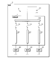
- FIG. 3 is a block diagram showing the main configuration of the power supply system 3. As shown in FIG.
- the power supply system 3 is mounted on the vehicle C.
- the power supply system 3 includes a circuit device 1 , three loads 30 and a DC power supply 31 .
- the load 30 is an electrical device.
- the DC power supply 31 is, for example, a battery.
- the bus bar 14 and the first conductive pattern 15 constitute the first conductor W1.
- the second conductive pattern 16 constitutes a second conductor W2.
- the circuit arrangement 1 has three first conductors W1 and second conductors W2. Three first conductors W1 of the circuit device 1 are connected to one ends of three loads 30, respectively.
- a fuse 13 connects the first conductor W1 and the second conductor W2.
- the second conductor W2 is further connected to the positive electrode of the DC power supply 31. As shown in FIG. The other ends of the three loads 30 and the negative pole of the DC power supply 31 are grounded.
- a current is input from the positive electrode of the DC power supply 31 to the second conductor W2.
- the current input to the second conductor W2 is divided into three currents.
- Each of the three shunted currents is output to the fuse 13 from the second conductor W2.
- the current output from the second conductor W2 flows through the fuse 13, the first conductor W1 and the load 30 in this order. Thereby, power is supplied to the load 30 .
- the load 30 performs various operations using power supplied from the DC power supply 31 .
- the first conductor W1 and the second conductor W2 each include the first conductive pattern 15 and the second conductive pattern 16. Therefore, the current flows through the second conductive pattern 16, the fuse 13 and the first conductive pattern 15 in this order.
- the circuit device 1 is arranged on a power supply path from a DC power supply 31 to a load 30 .
- the number of loads 30 connected to the circuit device 1 is the same as the number of fuses 13 .
- the number of fuses 13 is not limited to three. Therefore, the number of loads 30 is not limited to three either.
- FIG. 4 is a plan view of the circuit device 1 with the upper resist 11 removed.
- Each of the first conductive pattern 15 and the second conductive pattern 16 has a rectangular plate shape. As described above, the three first conductive patterns 15 are positioned behind the second conductive patterns 16 .
- a first conductor W ⁇ b>1 is configured by the bus bar 14 and the first conductive pattern 15 .
- the second conductive pattern 16 constitutes a second conductor W2.
- the positive electrode of the DC power supply 31 is connected to the second conductive pattern 16 (second conductor W2).
- the second terminals 21 b of the three fuses 13 are connected to the second conductive pattern 16 .
- the first terminals 21 a of the three fuses 13 are connected to the three first conductive patterns 15 .
- a first terminal 21 a of the fuse 13 is located at the front end of the first conductive pattern 15 .
- One end of a load 30 is connected to the rear end of the first conductive pattern 15 .
- the current flows through the fuse 13, the first conductor W1 and the load 30 in that order. Therefore, current flows from the front side to the rear side in the first conductive pattern 15 .
- the busbar 14 is arranged on the first conductive pattern 15 .
- the axial direction of the busbar 14 is the front-rear direction, and matches the current direction of the current flowing through the first conductive pattern 15 .
- FIG. 5 is a cross-sectional view of the circuit device 1 along line BB in FIG.
- FIG. 6 is a cross-sectional view of the circuit device 1 taken along line CC of FIG. 5 and 6 show cross sections of the circuit device 1 from which the upper resist 11 has been removed.
- the scales of FIGS. 5 and 6 are the same.
- the vertical direction perpendicular to the direction of current flowing through the first conductive pattern 15 is the horizontal direction.
- FIG. 5 shows a cross section of the first conductive pattern 15 in the vertical direction.
- FIG. 6 shows a vertical cross-section of the second conductive pattern 16 .
- the first conductive pattern 15 and the second conductive pattern 16 each have a rectangular cross section.
- the first conductive pattern 15 and the second conductive pattern 16 have the same height.
- the width of the first conductive pattern 15 is shorter than the width of the second conductive pattern 16 . Therefore, the cross-sectional area of the first conductive pattern 15 in the vertical direction is smaller than the cross-sectional area of the second conductive pattern 16 in the vertical direction.
- the height of the first conductive pattern 15 and the height of the second conductive pattern 16 should be substantially the same. Therefore, when the height difference between the first conductive pattern 15 and the second conductive pattern 16 is within the design error range, the heights of the first conductive pattern 15 and the second conductive pattern 16 are the same.
- the first conductive pattern 15 and the second conductive pattern 16 each have a resistance component. Therefore, when current flows through the first conductive pattern 15, the first conductive pattern 15 generates heat. When current flows through the second conductive pattern 16, the second conductive pattern 16 generates heat. The amount of heat generated by a conductor when current flows through the conductor increases as the resistance value of the conductor increases. The resistance value of a conductor decreases as the cross-sectional area of the conductor in the direction perpendicular to the direction of current flow increases.
- the cross-sectional area of the second conductive pattern 16 in the vertical direction is large. Therefore, the resistance value of the second conductive pattern 16 (second conductor W2) is small. Therefore, the amount of heat generated by the second conductor W2 is small.
- the cross-sectional area of the first conductive pattern 15 in the vertical direction is small. Therefore, the resistance value of the first conductive pattern 15 is large.
- the busbar 14 is arranged on the first conductive pattern 15 . Therefore, the current flows not only through the first conductive pattern 15 but also through the busbar 14 . Therefore, the resistance value of the first conductor W1 formed by the busbar 14 and the first conductive pattern 15 is the combined resistance value of the busbar 14 and the first conductive pattern 15, which is small. Therefore, the amount of heat generated by the first conductor W1 is small.
- the cross-sectional area of the first conductive pattern 15 is small, the effect obtained by arranging the bus bar 14 is great.
- the power consumption of a conductor is represented by the product of the square of the current value of the current flowing through the conductor and the resistance value of the conductor. Therefore, the greater the resistance value, the greater the amount of heat generated by the conductor.
- the axial direction of the busbar 14 matches the current direction. Therefore, when current flows through the first conductor W1, the section in which the current flows only through the first conductive pattern 15 is short.
- the first section is the area between the fuse 13 and the busbar 14 .
- the second section is a region from the rear end of bus bar 14 to the rear end of first conductive pattern 15 . The shorter the section where the current flows only through the first conductive pattern 15, the smaller the area where the amount of heat generated is large.
- the number of first conductors W1 is the same as the number of fuses 13. Therefore, the number of first conductors W1 may be one, or two or more.
- the current value of the current flowing through the second conductive pattern 16 is large. Therefore, a conductor having a large cross-sectional area is used as the second conductive pattern 16 .
- the number of first conductive patterns 15 is large. Therefore, a conductor with a small cross-sectional area is used as the first conductive pattern 15 .
- a conductor with a small cross-sectional area has a large resistance value. Therefore, the effect obtained by arranging the bus bar 14 is great. If the bus bar 14 is not used, it is necessary to use a conductive pattern with a large cross-sectional area as the first conductive pattern 15 . In this case, the number of loads 30 that can be connected to the circuit device 1 is limited.
- the shape of one first conductive pattern 15 may be different from the shape of one of the remaining first conductive patterns 15 .
- the length in the horizontal direction of one first conductive pattern 15 may be different from the length in the horizontal direction of one of the remaining first conductive patterns 15 .
- the length in the front-rear direction of one first conductive pattern 15 may be different from the length in the front-rear direction of one of the remaining first conductive patterns 15 .
- Embodiment 2 In Embodiment 1, the number of bus bars 14 arranged on the common first conductive pattern 15 is one. However, the number of busbars 14 arranged on the common first conductive pattern 15 may be two or more.
- the points of the second embodiment that are different from the first embodiment will be described. Configurations other than those described later are the same as those of the first embodiment. For this reason, the same reference numerals as in the first embodiment are assigned to the components that are common to the first embodiment, and the description thereof is omitted.
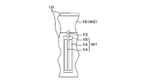
- FIG. 7 is an explanatory diagram of the arrangement of the busbars 14 according to the second embodiment.
- two busbars 14 are arranged on the common first conductive pattern 15 .
- the axial directions of the two bus bars 14 match the current direction of the current flowing through the first conductive pattern 15 as in the second embodiment.
- the two busbars 14 are arranged in a vertical direction (horizontal direction) perpendicular to the current direction.
- the two busbars 14 and the first conductive pattern 15 constitute the first conductor W1.
- the two busbars 14 arranged on the common first conductive pattern 15 are separated.
- the axial directions of the two busbars 14 match the current direction. Therefore, the amount of heat generated by the first conductor W1 when current flows through the first conductor W1 is even smaller.
- mass-produced busbars can be used as the busbars 14 .
- the circuit device 1 according to the second embodiment has the same effect as the circuit device 1 according to the first embodiment.
- the number of busbars 14 arranged on the common first conductive pattern 15 is not limited to two. Three or more busbars 14 may be arranged vertically. As the number of bus bars 14 increases, a conductive pattern having a smaller cross-sectional area can be used as the first conductive pattern 15 . Also, two busbars 14 arranged in the vertical direction may be in contact with each other.
- a plurality of busbars 14 are vertically arranged on the common first conductive pattern 15 .
- the direction in which the plurality of busbars 14 are arranged is not limited to the vertical direction.
- Configurations other than those described later are the same as those of the second embodiment. For this reason, the same reference numerals as in the second embodiment are assigned to the components that are common to the second embodiment, and the description thereof is omitted.
- FIG. 8 is an explanatory diagram of the arrangement of the busbars 14 according to the third embodiment.
- two busbars 14 are arranged on a common first conductive pattern 15 .
- the two bus bars 14 are arranged in the current direction (front-rear direction) of the current flowing through the first conductive pattern 15 .
- the two busbars 14 are in contact.
- the axial directions of the two busbars 14 match the current direction. Therefore, the amount of heat generated by the first conductor W1 when a current flows through the first conductor W1 is small as in the second embodiment.
- Each of the two busbars 14 is arranged along the current direction. Therefore, when the current flows through the first conductor W1, the section in which the current flows only through the first conductive pattern 15 is even shorter.
- mass-produced busbars can be used as the busbars 14 .
- the circuit device 1 of the third embodiment has the same effects except for the effect obtained by arranging the plurality of bus bars 14 in the vertical direction.
- the number of busbars 14 arranged on the common first conductive pattern 15 is not limited to two. Three or more busbars 14 may be arranged in the current direction. As the number of bus bars 14 increases, a conductive pattern having a smaller vertical cross-sectional area can be used as the first conductive pattern 15 . Also, the two busbars 14 arranged in the current direction may be separated from each other. Furthermore, the arrangement of the two busbars 14 arranged in the current direction is not limited to the arrangement in which the two busbars 14 are arranged in a straight line. The shaft of the other busbar 14 may be arranged on a line different from the extension line of the shaft of one busbar 14 .
- a plurality of busbars 14 are vertically arranged on the common first conductive pattern 15 . Further, in the second embodiment, a plurality of busbars 14 may be arranged in the current direction on the first conductive pattern 15 as in the third embodiment.
- the points of the fourth embodiment that are different from the second embodiment will be described. Configurations other than those described later are the same as those of the second embodiment. For this reason, the same reference numerals as in the second embodiment are assigned to the components that are common to the second embodiment, and the description thereof is omitted.
- FIG. 9 is an explanatory diagram of the arrangement of the busbars 14 according to the fourth embodiment.
- three bus bars 14 are arranged on a common first conductive pattern 15 .
- Two of the three busbars 14 are arranged vertically as in the second embodiment.
- two of the three busbars 14 are arranged in the current direction, as in the third embodiment.
- three busbars 14 are arranged in a zigzag pattern on the common first conductive pattern 15 .
- the circuit device 1 according to the fourth embodiment has the same effect as the circuit devices 1 according to the second and third embodiments.
- the number of bus bars 14 arranged on the common first conductive pattern 15 is not limited to three, and may be four or more. As the number of bus bars 14 increases, a conductive pattern having a smaller vertical cross-sectional area can be used as the first conductive pattern 15 .
- the number of busbars 14 arranged in the vertical direction is not limited to two, and may be three or more.
- the number of bus bars 14 arranged in the current direction is not limited to two, and may be three or more.
- the arrangement of the plurality of busbars 14 on the common first conductive pattern 15 is not limited to the zigzag arrangement, and may be a lattice arrangement.
- the two vertically arranged busbars 14 may be in contact with each other or may be separated from each other.
- the two busbars 14 arranged in the current direction may be in contact with each other or may be separated from each other.
- the number of bus bars 14 arranged on the common first conductive pattern 15 may be one, or two or more.
- the number of bus bars 14 arranged on one first conductive pattern 15 is the same as the number of bus bars 14 arranged on the upper surface of one of the remaining first conductive patterns 15. may be different from the number of
- the plurality of first conductors W1 of the circuit device 1 may include at least two of the first conductors W1 of the first to fourth embodiments.
- the first conductor W1 is composed of at least one bus bar 14 and one first conductive pattern 15. As shown in FIG.
- the second conductor W ⁇ b>2 in the first embodiment is composed only of the second conductive pattern 16 .
- a conductor different from the second conductive pattern 16 may be included as a component of the second conductor W2.
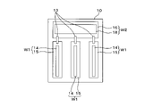
- FIG. 10 is a plan view of the circuit device 1 according to Embodiment 5.
- the second bus bar 18 is arranged on the second conductive pattern 16 .
- the second conductive pattern 16 is electrically connected to the second bus bar 18 .
- the second conductor W2 is composed of the second conductive pattern 16 and the second bus bar 18 .
- the circuit device 1 according to the fifth embodiment has the same effect as the circuit device 1 according to the first embodiment.
- the number of first conductive patterns 15 is three.
- the number of bus bars 14 arranged on the common first conductive pattern 15 is one.
- Each first conductor W1 is composed of a first conductive pattern 15 and one busbar 14 .
- the number of first conductive patterns 15 is not limited to three.
- the number of bus bars 14 arranged on the common first conductive pattern 15 is not limited to one.
- the configuration of each of all first conductors W1 is not limited to the configuration in which one bus bar 14 is arranged on the first conductive pattern 15.
- the number of second bus bars 18 arranged on the second conductive pattern 16 is not limited to one, and may be two or more. As the number of second bus bars 18 increases, a conductive pattern having a smaller vertical cross-sectional area can be used as the second conductive pattern 16 .
- the shape of one second busbar 18 may be different from the shape of one of the remaining second busbars 18 .
- the second conductor W ⁇ b>2 is composed of the second conductive pattern 16 and the plurality of second busbars 18 . In a similar case, multiple second busbars 18 may be stacked.
- the bus bar 14 may have a cross section with a shape different from a rectangular shape.
- the shape of one busbar 14 may be different from the shape of one of the remaining busbars 14.
- FIG. 1 when a plurality of busbars 14 are arranged on the common first conductive pattern 15, the plurality of busbars 14 may be stacked.
- the circuit element connecting the first conductive pattern 15 and the second conductive pattern 16 is not limited to the fuse 13.
- a PTC thermistor may be used instead of the fuse 13 as a first example of the circuit element.
- the PTC thermistor like the fuse 13, prevents overcurrent flow. When current flows through a PTC thermistor, it heats up. When the temperature of the PTC thermistor rises, the resistance value of the PTC thermistor rises. When the resistance value of the PTC thermistor increases, the current value of the current flowing through the second conductive pattern 16, the circuit element (PTC thermistor), and the first conductive pattern 15 decreases.
- the fuse 13 is preferable as an element for preventing overcurrent flow.
- a circuit element such as a semiconductor switch, resistor or inductor may connect the first conductive pattern 15 and the second conductive pattern 16 .
- a series circuit of semiconductor switches and fuses 13 may connect the first conductive pattern 15 and the second conductive pattern 16 . If a semiconductor switch is used as the circuit element, the semiconductor switch may be switched off when the ambient temperature of the first conductor W1 reaches a temperature above a certain temperature threshold. At this time, the semiconductor switch functions as a fuse.
- circuit elements such as semiconductor switches, resistors, or inductors may change depending on the temperature of the circuit elements. Even in this case, the amount of heat generated by the first conductor W1 is small in the circuit device 1 according to each of the first to fifth embodiments. Therefore, the temperature of the circuit element hardly changes due to the heat generated by the first conductor W1, so the circuit element operates properly.
- circuit device 3 power supply system 10 insulating layer 10a first through hole 10b second through hole 11 upper resist 12 lower resist 13 fuse (circuit element) 14 bus bar 15 first conductive pattern (conductor) 16 Second conductive pattern 17a First plating 17b Second plating 18 Second bus bar 20 Fuse body 21a First terminal 21b Second terminal 30 Load 31 DC power supply C Vehicle H Solder W1 First conductor W2 Second conductor
Landscapes
- Engineering & Computer Science (AREA)
- Microelectronics & Electronic Packaging (AREA)
- Fuses (AREA)
- Mechanical Engineering (AREA)
Abstract
Description
本出願は、2021年3月9日出願の日本出願第2021-037554号に基づく優先権を主張し、前記日本出願に記載された全ての記載内容を援用するものである。
導体を介して電流が流れた場合、導体は発熱する。導体の発熱量が大きい場合、導体が発する熱によって溶断素子の温度が上昇する。この場合、溶断素子に想定外の熱が加えられるため、溶断素子が適切なタイミングで溶断されない可能性がある。溶断素子とは異なる回路素子が用いられる場合であっても、回路素子の特性が回路素子の温度に応じて変化するとき、回路素子は適切に作用しない可能性がある。
本開示によれば、導体を介して電流が流れた場合における導体の発熱量が小さい。
最初に本開示の実施態様を列挙して説明する。以下に記載する実施形態の少なくとも一部を任意に組み合わせてもよい。
本開示の実施形態に係る回路装置の具体例を、以下に図面を参照しつつ説明する。なお、本発明はこれらの例示に限定されるものではなく、請求の範囲によって示され、請求の範囲と均等の意味および範囲内でのすべての変更が含まれることが意図される。
<回路装置の外観>
図1は実施形態1における回路装置1の斜視図である。回路装置1では、絶縁性を有する矩形板状の絶縁層10の上面は、上側レジスト11によって覆われている。絶縁層10の下面は下側レジスト12によって覆われている。絶縁層の上面及び下面それぞれは主面である。板に関しては、主面は、幅が広い面であり、端面とは異なる。上側レジスト11及び下側レジスト12それぞれは、絶縁性を有する。上側レジスト11及び下側レジスト12は例えば樹脂製である。
図2は、図1のA-A線における回路装置1の部分断面図である。回路装置1では、絶縁層10の上面に、導電性を有する第1導電パターン15及び第2導電パターン16が配置されている。第1導電パターン15は、第2導電パターン16の後側に位置する。絶縁層10には、上下方向に貫通する第1貫通孔10a及び第2貫通孔10bが設けられている。第1貫通孔10aは第2貫通孔10bの後側に位置する。
以上のように、ヒューズ13は、第1導電パターン15及び第2導電パターン16を接続する。
図3は電源システム3の要部構成を示すブロック図である。電源システム3は車両Cに搭載されている。電源システム3は、回路装置1、3つの負荷30及び直流電源31を備える。負荷30は電気機器である。直流電源31は例えばバッテリである。
図4は、上側レジスト11が除かれた回路装置1の平面図である。第1導電パターン15及び第2導電パターン16それぞれは矩形板状をなす。前述したように、3つの第1導電パターン15は、第2導電パターン16の後側に位置する。バスバー14及び第1導電パターン15によって第1導体W1が構成されている。第2導電パターン16によって第2導体W2が構成されている。
なお、ここで、バスバー14の軸方向及び電流方向の一致は実質的に実現されていればよい。従って、軸方向及び電流方向がなす角度が設計上の誤差範囲内の値である場合、軸方向及び電流方向は一致している。
第1導電パターン15の数が2以上である場合において、1つの第1導電パターン15の形状は、残りの第1導電パターン15中の1つの形状と異なっていてもよい。第1例として、1つの第1導電パターン15の左右方向の長さは、残りの第1導電パターン15中の1つの左右方向の長さと異なっていてもよい。第2例として、1つの第1導電パターン15の前後方向の長さは、残りの第1導電パターン15中の1つの前後方向の長さと異なっていてもよい。
実施形態1では、共通の第1導電パターン15上に配置されるバスバー14の数は1である。しかしながら、共通の第1導電パターン15上に配置されるバスバー14の数は2以上であってもよい。
以下では、実施形態2について、実施形態1と異なる点を説明する。後述する構成を除く他の構成は実施形態1と共通している。このため、実施形態1と共通する構成部には、実施形態1と同一の参照符号を付してその説明を省略する。
図7は、実施形態2におけるバスバー14の配置の説明図である。実施形態2における回路装置1では、共通の第1導電パターン15上に2つのバスバー14が配置されている。2つのバスバー14の軸方向は、実施形態2と同様に、第1導電パターン15を介して流れる電流の電流方向と一致している。2つのバスバー14は、電流方向に垂直な垂直方向(左右方向)に並べられている。実施形態2では、2つのバスバー14及び第1導電パターン15によって第1導体W1が構成されている。図7の例では、共通の第1導電パターン15上に配置される2つのバスバー14は離されている。
実施形態2における回路装置1は、実施形態1における回路装置1と同様の効果を奏する。
共通の第1導電パターン15上に配置されるバスバー14の数は2に限定されない。3つ以上のバスバー14を垂直方向に並べてもよい。バスバー14の数が多い程、第1導電パターン15として、断面積がより小さい導電パターンを用いることができる。また、垂直方向に並べられている2つのバスバー14は互いに接触していてもよい。
実施形態2では、共通の第1導電パターン15上において、複数のバスバー14が垂直方向に並べられている。しかしながら、複数のバスバー14の並び方向は垂直方向に限定されない。
以下では、実施形態3について、実施形態2と異なる点を説明する。後述する構成を除く他の構成は実施形態2と共通している。このため、実施形態2と共通する構成部には、実施形態2と同一の参照符号を付してその説明を省略する。
図8は、実施形態3におけるバスバー14の配置の説明図である。実施形態3では、共通の第1導電パターン15上に2つのバスバー14が並べられている。2つのバスバー14は、第1導電パターン15を介して流れる電流の電流方向(前後方向)に並べられている。図8の例では、2つのバスバー14は接触している。
共通の第1導電パターン15上に配置されるバスバー14の数は2に限定されない。3つ以上のバスバー14を電流方向に並べてもよい。バスバー14の数が多い程、第1導電パターン15として、垂直方向の断面積がより小さい導電パターンを用いることができる。また、電流方向に並べられている2つのバスバー14は離れていてもよい。更に、電流方向に並べられている2つバスバー14の配置に関する構成は、一直線上に2つのバスバー14が配置される構成に限定されない。一方のバスバー14の軸の延長線とは異なる線上に他方のバスバー14の軸が配置されてもよい。
実施形態2では、共通の第1導電パターン15上において、複数のバスバー14が垂直方向に並べられている。実施形態2では、更に、複数のバスバー14が、第1導電パターン15上において、実施形態3と同様に電流方向に並べられてもよい。
以下では、実施形態4について、実施形態2と異なる点を説明する。後述する構成を除く他の構成は実施形態2と共通している。このため、実施形態2と共通する構成部には、実施形態2と同一の参照符号を付してその説明を省略する。
図9は、実施形態4におけるバスバー14の配置の説明図である。実施形態4における回路装置1では、3つのバスバー14が共通の第1導電パターン15上に並べられている。3つのバスバー14中の2つは、実施形態2と同様に、垂直方向に並べられている。更に、3つのバスバー14中の2つは、実施形態3と同様に、電流方向に並べられている。図9の例では、共通の第1導電パターン15上において、3つのバスバー14は、千鳥状に配置されている。
実施形態4において、共通の第1導電パターン15上に配置されるバスバー14の数は、3に限定されず、4以上であってもよい。バスバー14の数が多い程、第1導電パターン15として、垂直方向の断面積がより小さい導電パターンを用いることができる。垂直方向に並べられるバスバー14の数は、2に限定されず、3以上であってもよい。電流方向に並べられるバスバー14の数は、2に限定されず、3以上であってもよい。共通の第1導電パターン15上における複数のバスバー14の配置は、千鳥状の配置に限定されず、格子状の配置であってもよい。実施形態2と同様に、垂直方向に並べられる2つのバスバー14は、接触していてもよいし、離されていてもよい。実施形態3と同様に、電流方向に並べられる2つのバスバー14は、接触していてもよいし、離されていてもよい。
前述したように、実施形態1において、共通の第1導電パターン15上に配置されるバスバー14の数は、1であってもよいし、2以上であってもよい。第1導体W1の数が2以上である場合において、1つの第1導電パターン15上に配置されるバスバー14の数は、残りの第1導電パターン15中の1つの上面に配置されるバスバー14の数と異なっていてもよい。
実施形態1における第2導体W2は、第2導電パターン16のみによって構成されている。しかしながら、第2導体W2の構成要素として、第2導電パターン16とは異なる導体が含まれていてもよい。
以下では、実施形態2について、実施形態1と異なる点を説明する。後述する構成を除く他の構成は実施形態1と共通している。このため、実施形態1と共通する構成部には、実施形態1と同一の参照符号を付してその説明を省略する。
実施形態5における回路装置1は、実施形態1における回路装置1が奏する効果を同様に奏する。
第2導電パターン16上に配置される第2のバスバー18の数は、1に限定されず、2以上であってもよい。第2のバスバー18の数が多い程、第2導電パターン16として、垂直方向の断面積がより小さい導電パターンを用いることができる。第2導電パターン16上に複数の第2のバスバー18が配置される場合、1つの第2のバスバー18の形状は、残りの第2のバスバー18中の1つの形状と異なっていてもよい。第2導電パターン16上に複数の第2のバスバー18が配置される場合、第2導体W2は、第2導電パターン16及び複数の第2のバスバー18によって構成される。同様の場合において、複数の第2のバスバー18を積み重ねてもよい。
実施形態1~5それぞれにおいて、バスバー14は、矩形状とは異なる形状の断面を有していてもよい。実施形態1~5それぞれにおいて、回路装置1が複数のバスバー14を有する場合、1つのバスバー14の形状は、残りのバスバー14中の1つの形状と異なっていてもよい。実施形態2~5それぞれにおいて、共通の第1導電パターン15上に複数のバスバー14が配置される場合、複数のバスバー14を積み重ねてもよい。
3 電源システム
10 絶縁層
10a 第1貫通孔
10b 第2貫通孔
11 上側レジスト
12 下側レジスト
13 ヒューズ(回路素子)
14 バスバー
15 第1導電パターン(導体)
16 第2導電パターン
17a 第1メッキ
17b 第2メッキ
18 第2のバスバー
20 ヒューズ本体
21a 第1端子
21b 第2端子
30 負荷
31 直流電源
C 車両
H 半田
W1 第1導体
W2 第2導体
Claims (8)
- 電力の供給経路に配置される車両用の回路装置であって、
絶縁層と、
前記絶縁層上に配置される第1導電パターン及び第2導電パターンと、
前記第1導電パターン及び第2導電パターンを接続する回路素子と、
前記第1導電パターン上に配置されるバスバーと
を備える回路装置。 - 前記回路素子はヒューズである
請求項1に記載の回路装置。 - 電流は、前記第2導電パターン、回路素子及び第1導電パターンの順に流れ、
前記第1導電パターンを介して流れる電流の電流方向に垂直な垂直方向の前記第1導電パターンの断面積は、前記垂直方向の前記第2導電パターンの断面積よりも小さい
請求項1又は請求項2に記載の回路装置。 - 電流は、前記第2導電パターン、回路素子及び第1導電パターンの順に流れ、
前記バスバーの軸方向は、前記第1導電パターンを介して流れる電流の電流方向と一致している
請求項1から請求項3のいずれか1項に記載の回路装置。 - 前記バスバーの数は2以上であり、
複数のバスバーは、前記電流方向に垂直な垂直方向に並べられている
請求項4に記載の回路装置。 - 前記バスバーの数は、2以上であり、
複数のバスバーは、前記電流方向に並べられている
請求項4又は請求項5に記載の回路装置。 - 前記第2導電パターン上に配置される第2のバスバーを備える
請求項1から請求項6のいずれか1項に記載の回路装置。 - 前記第1導電パターン及び回路素子それぞれの数は2以上であり、
複数の回路素子は前記第2導電パターンに接続され、
複数の回路素子それぞれは複数の第1導電パターンに接続される
請求項1から請求項7のいずれか1項に記載の回路装置。
Priority Applications (3)
| Application Number | Priority Date | Filing Date | Title |
|---|---|---|---|
| US18/548,440 US20240153729A1 (en) | 2021-03-09 | 2022-02-21 | Circuit device |
| CN202280016040.8A CN116918026A (zh) | 2021-03-09 | 2022-02-21 | 电路装置 |
| DE112022001404.0T DE112022001404T5 (de) | 2021-03-09 | 2022-02-21 | Schaltvorrichtung |
Applications Claiming Priority (2)
| Application Number | Priority Date | Filing Date | Title |
|---|---|---|---|
| JP2021037554A JP7578028B2 (ja) | 2021-03-09 | 2021-03-09 | 回路装置 |
| JP2021-037554 | 2021-03-09 |
Publications (1)
| Publication Number | Publication Date |
|---|---|
| WO2022190837A1 true WO2022190837A1 (ja) | 2022-09-15 |
Family
ID=83227757
Family Applications (1)
| Application Number | Title | Priority Date | Filing Date |
|---|---|---|---|
| PCT/JP2022/006950 Ceased WO2022190837A1 (ja) | 2021-03-09 | 2022-02-21 | 回路装置 |
Country Status (5)
| Country | Link |
|---|---|
| US (1) | US20240153729A1 (ja) |
| JP (1) | JP7578028B2 (ja) |
| CN (1) | CN116918026A (ja) |
| DE (1) | DE112022001404T5 (ja) |
| WO (1) | WO2022190837A1 (ja) |
Citations (4)
| Publication number | Priority date | Publication date | Assignee | Title |
|---|---|---|---|---|
| JP2005235551A (ja) * | 2004-02-19 | 2005-09-02 | Auto Network Gijutsu Kenkyusho:Kk | ヒューズモジュール |
| JP2015204226A (ja) * | 2014-04-15 | 2015-11-16 | デクセリアルズ株式会社 | 保護素子 |
| JP2017027831A (ja) * | 2015-07-24 | 2017-02-02 | 株式会社オートネットワーク技術研究所 | 電池配線モジュール |
| WO2020194967A1 (ja) * | 2019-03-27 | 2020-10-01 | 三洋電機株式会社 | 過電流保護素子とバッテリーシステム |
Family Cites Families (11)
| Publication number | Priority date | Publication date | Assignee | Title |
|---|---|---|---|---|
| US5099219A (en) * | 1991-02-28 | 1992-03-24 | Rock, Ltd. Partnership | Fusible flexible printed circuit and method of making same |
| JPH10199396A (ja) * | 1997-01-13 | 1998-07-31 | Taiheiyo Seiko Kk | 多極型ヒューズ素子およびこの素子を使用した多極型ヒューズ |
| US6456186B1 (en) * | 1999-10-27 | 2002-09-24 | Motorola, Inc. | Multi-terminal fuse device |
| US7351911B2 (en) * | 2001-04-27 | 2008-04-01 | Yazaki Corporation | Connection box |
| US6961515B2 (en) * | 2002-02-15 | 2005-11-01 | Dekko Technologies, Inc. | PTC heater with flexible printed circuit board |
| JP4923841B2 (ja) | 2006-08-11 | 2012-04-25 | 住友電装株式会社 | 電気接続箱に収容する回路材および該回路材を収容する車載用の電気接続箱 |
| JP2008054449A (ja) | 2006-08-25 | 2008-03-06 | Sumitomo Wiring Syst Ltd | 電気接続箱に収容する回路材 |
| JP6255158B2 (ja) * | 2013-02-12 | 2017-12-27 | 矢崎総業株式会社 | バスバー |
| US10796873B2 (en) * | 2017-12-15 | 2020-10-06 | Nio Usa, Inc. | Fusible link in battery module voltage sensing circuit |
| JP6577118B2 (ja) | 2018-10-23 | 2019-09-18 | デクセリアルズ株式会社 | ヒューズエレメント、ヒューズ素子、保護素子、短絡素子、切替素子 |
| JP2021037554A (ja) | 2019-08-30 | 2021-03-11 | 株式会社カワタテック | 工具交換装置 |
-
2021
- 2021-03-09 JP JP2021037554A patent/JP7578028B2/ja active Active
-
2022
- 2022-02-21 DE DE112022001404.0T patent/DE112022001404T5/de active Pending
- 2022-02-21 CN CN202280016040.8A patent/CN116918026A/zh active Pending
- 2022-02-21 US US18/548,440 patent/US20240153729A1/en not_active Abandoned
- 2022-02-21 WO PCT/JP2022/006950 patent/WO2022190837A1/ja not_active Ceased
Patent Citations (4)
| Publication number | Priority date | Publication date | Assignee | Title |
|---|---|---|---|---|
| JP2005235551A (ja) * | 2004-02-19 | 2005-09-02 | Auto Network Gijutsu Kenkyusho:Kk | ヒューズモジュール |
| JP2015204226A (ja) * | 2014-04-15 | 2015-11-16 | デクセリアルズ株式会社 | 保護素子 |
| JP2017027831A (ja) * | 2015-07-24 | 2017-02-02 | 株式会社オートネットワーク技術研究所 | 電池配線モジュール |
| WO2020194967A1 (ja) * | 2019-03-27 | 2020-10-01 | 三洋電機株式会社 | 過電流保護素子とバッテリーシステム |
Also Published As
| Publication number | Publication date |
|---|---|
| JP7578028B2 (ja) | 2024-11-06 |
| JP2022137860A (ja) | 2022-09-22 |
| CN116918026A (zh) | 2023-10-20 |
| DE112022001404T5 (de) | 2024-01-11 |
| US20240153729A1 (en) | 2024-05-09 |
Similar Documents
| Publication | Publication Date | Title |
|---|---|---|
| CN107851754B (zh) | 电池配线模块 | |
| US8310085B2 (en) | Electrical junction box for vehicle | |
| JP4381845B2 (ja) | ヒューズモジュール | |
| US8891220B2 (en) | Overcurrent cutoff device, and overcurrent detecting element to be used in overcurrent cutoff device | |
| US5818676A (en) | Multiple element PTC overcurrent protection device | |
| CN111095468B (zh) | 低轮廓集成熔断器模块 | |
| PT82968B (pt) | Dispositivo para ligacao centralizada de componentes electricos de um automovel | |
| JP2018142435A (ja) | 温度ヒューズ及び電気接続箱 | |
| CN103715575B (zh) | 汇流排的布置结构 | |
| US6667461B1 (en) | Multiple load protection and control device | |
| KR101766953B1 (ko) | 제어장치 | |
| JP7578028B2 (ja) | 回路装置 | |
| CN112534539A (zh) | 低剖面集成熔断器模块 | |
| JP2002078144A (ja) | 電気接続箱 | |
| CN102194621B (zh) | 熔丝单元 | |
| JP7661862B2 (ja) | 給電制御装置 | |
| CN117501397A (zh) | 车载装置 | |
| CN202275674U (zh) | 具有过电流断路功能的电阻 | |
| JP7609822B2 (ja) | バスバー | |
| US11749483B1 (en) | Fuse with compartmentalized body and parallel fuse elements | |
| KR19980024524A (ko) | 과부하 보호 릴레이 | |
| US6154118A (en) | Circuit protective device with positive temperature coefficient element and electric junction box with the device | |
| US6204451B1 (en) | Electrical wiring construction including a bus bar | |
| EP0939454B1 (en) | Electrical wiring construction including a bus bar | |
| CN204497170U (zh) | 用于脱扣器的发热件、脱扣器及断路器 |
Legal Events
| Date | Code | Title | Description |
|---|---|---|---|
| 121 | Ep: the epo has been informed by wipo that ep was designated in this application |
Ref document number: 22766800 Country of ref document: EP Kind code of ref document: A1 |
|
| WWE | Wipo information: entry into national phase |
Ref document number: 202280016040.8 Country of ref document: CN |
|
| WWE | Wipo information: entry into national phase |
Ref document number: 18548440 Country of ref document: US |
|
| WWE | Wipo information: entry into national phase |
Ref document number: 112022001404 Country of ref document: DE |
|
| 122 | Ep: pct application non-entry in european phase |
Ref document number: 22766800 Country of ref document: EP Kind code of ref document: A1 |