WO2022190708A1 - コンデンサモジュール - Google Patents
コンデンサモジュール Download PDFInfo
- Publication number
- WO2022190708A1 WO2022190708A1 PCT/JP2022/003632 JP2022003632W WO2022190708A1 WO 2022190708 A1 WO2022190708 A1 WO 2022190708A1 JP 2022003632 W JP2022003632 W JP 2022003632W WO 2022190708 A1 WO2022190708 A1 WO 2022190708A1
- Authority
- WO
- WIPO (PCT)
- Prior art keywords
- capacitor
- electrode
- bus bar
- sensor
- capacitor module
- Prior art date
- Legal status (The legal status is an assumption and is not a legal conclusion. Google has not performed a legal analysis and makes no representation as to the accuracy of the status listed.)
- Ceased
Links
Images








Classifications
-
- H—ELECTRICITY
- H01—ELECTRIC ELEMENTS
- H01G—CAPACITORS; CAPACITORS, RECTIFIERS, DETECTORS, SWITCHING DEVICES, LIGHT-SENSITIVE OR TEMPERATURE-SENSITIVE DEVICES OF THE ELECTROLYTIC TYPE
- H01G2/00—Details of capacitors not covered by a single one of groups H01G4/00-H01G11/00
- H01G2/02—Mountings
-
- H—ELECTRICITY
- H01—ELECTRIC ELEMENTS
- H01G—CAPACITORS; CAPACITORS, RECTIFIERS, DETECTORS, SWITCHING DEVICES, LIGHT-SENSITIVE OR TEMPERATURE-SENSITIVE DEVICES OF THE ELECTROLYTIC TYPE
- H01G2/00—Details of capacitors not covered by a single one of groups H01G4/00-H01G11/00
- H01G2/02—Mountings
- H01G2/04—Mountings specially adapted for mounting on a chassis
-
- H—ELECTRICITY
- H01—ELECTRIC ELEMENTS
- H01G—CAPACITORS; CAPACITORS, RECTIFIERS, DETECTORS, SWITCHING DEVICES, LIGHT-SENSITIVE OR TEMPERATURE-SENSITIVE DEVICES OF THE ELECTROLYTIC TYPE
- H01G2/00—Details of capacitors not covered by a single one of groups H01G4/00-H01G11/00
- H01G2/14—Protection against electric or thermal overload
-
- H—ELECTRICITY
- H01—ELECTRIC ELEMENTS
- H01G—CAPACITORS; CAPACITORS, RECTIFIERS, DETECTORS, SWITCHING DEVICES, LIGHT-SENSITIVE OR TEMPERATURE-SENSITIVE DEVICES OF THE ELECTROLYTIC TYPE
- H01G4/00—Fixed capacitors; Processes of their manufacture
- H01G4/002—Details
- H01G4/018—Dielectrics
- H01G4/06—Solid dielectrics
- H01G4/14—Organic dielectrics
- H01G4/18—Organic dielectrics of synthetic material, e.g. derivatives of cellulose
-
- H—ELECTRICITY
- H01—ELECTRIC ELEMENTS
- H01G—CAPACITORS; CAPACITORS, RECTIFIERS, DETECTORS, SWITCHING DEVICES, LIGHT-SENSITIVE OR TEMPERATURE-SENSITIVE DEVICES OF THE ELECTROLYTIC TYPE
- H01G4/00—Fixed capacitors; Processes of their manufacture
- H01G4/32—Wound capacitors
-
- H—ELECTRICITY
- H01—ELECTRIC ELEMENTS
- H01G—CAPACITORS; CAPACITORS, RECTIFIERS, DETECTORS, SWITCHING DEVICES, LIGHT-SENSITIVE OR TEMPERATURE-SENSITIVE DEVICES OF THE ELECTROLYTIC TYPE
- H01G4/00—Fixed capacitors; Processes of their manufacture
- H01G4/38—Multiple capacitors, i.e. structural combinations of fixed capacitors
Definitions
- the present invention relates to capacitor modules.
- Patent Document 1 a capacitor module is being studied in which a temperature sensor is arranged in the case to detect the overheating state of the capacitor.
- Patent Document 1 The capacitor described in Patent Document 1 has a problem that it is difficult to miniaturize the capacitor module.
- an object of the present invention is to provide a capacitor module that can be easily miniaturized.
- a capacitor module includes A capacitor module having a plurality of capacitors, A wound body of a dielectric film, comprising a first electrode, a second electrode facing the first electrode, a pair of flat portions connecting the first electrode and the second electrode, and a pair of flat portions facing each other a first capacitor having a first side surface with curved portions connecting each other; A wound body of a dielectric film, comprising a third electrode, a fourth electrode facing the third electrode, a pair of flat portions connecting the third electrode and the fourth electrode, and a pair of flat portions facing each other a second capacitor having a second side surface with curved portions connecting each other; a first bus bar having a support surface supporting the first side surface and the second side surface and electrically connected to the first electrode of the first capacitor and the third electrode of the second capacitor; a second bus bar electrically connected to the second electrode of the first capacitor and the fourth electrode of the second capacitor; a sensor having a detection unit for detecting an abnormality related to the capacitor module; with The first side surface of the first side surface of the first electrode
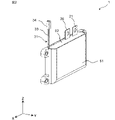
- FIG. 1 is a plan view of a capacitor module according to Embodiment 1 of the present invention
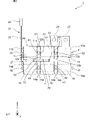
- a perspective view of the capacitor module of FIG. FIG. 2 is a plan view of the capacitor module in FIG. 1 omitting the case and sealing resin
- FIG. 2 is a perspective view showing a first capacitor of the capacitor module of FIG. 1
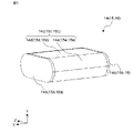
- 2 is a perspective view showing a second capacitor of the capacitor module of FIG. 1
- FIG. 2 is a perspective view showing a first protrusion, a second protrusion, and a support member of the capacitor module of FIG.
- FIG. 7A 2 is a perspective view showing a sensor of the capacitor module of FIG. 1;
- FIG. FIG. 2 is a partial enlarged view showing a modification of the support member of the capacitor module of FIG. 1;
- FIG. 2 is a partial enlarged view showing a modification of the support member of the capacitor module of FIG. 1;
- FIG. 2 is a partial enlarged view showing a modification of the support member of the capacitor module of FIG. 1;
- FIG. 2 is a partial enlarged view showing a modification of the support member of the capacitor module of FIG. 1;
- FIG. 2 is a partial enlarged view showing a modification of the support member of the capacitor module of FIG. 1;
- a perspective view of a capacitor module according to a second embodiment The figure which looked at the capacitor module of FIG. 10 from the X direction Enlarged view of part of FIG. 11A Plan view of the capacitor module of FIG.
- the capacitor arranged in the center is difficult to dissipate heat and becomes hotter than the other capacitors, which may cause malfunction of the capacitor. Also, overcurrent may cause problems in the capacitor module. Therefore, like the capacitor module described in Patent Document 1, by arranging a sensor in the case, detecting an abnormality of the capacitor such as high temperature or overcurrent has been studied.
- the present inventors have studied the configuration of a capacitor module that can be easily miniaturized, and have arrived at the following invention.
- a capacitor module includes A capacitor module having a plurality of capacitors, A wound body of a dielectric film, comprising a first electrode, a second electrode facing the first electrode, a pair of flat portions connecting the first electrode and the second electrode, and a pair of flat portions facing each other a first capacitor having a first side surface with curved portions connecting each other; A wound body of a dielectric film, comprising a third electrode, a fourth electrode facing the third electrode, a pair of flat portions connecting the third electrode and the fourth electrode, and a pair of flat portions facing each other a second capacitor having a second side surface with curved portions connecting each other; a first bus bar having a support surface supporting the first side surface and the second side surface and electrically connected to the first electrode of the first capacitor and the third electrode of the second capacitor; a second bus bar electrically connected to the second electrode of the first capacitor and the fourth electrode of the second capacitor; a sensor having a detection unit for detecting an abnormality related to the capacitor module; with The first side surface of the first side surface of the first electrode
- sensors can be arranged using dead space while enabling anomaly detection. Therefore, it is possible to provide a capacitor module that can be easily miniaturized without affecting the design of the capacitor module.
- the sensor has an elongated part with a detection part at the tip, The elongated portion may be arranged in the space.
- the detection unit can be arranged near the center of the capacitor module, so the sensitivity of abnormality detection can be improved.
- the first busbar may have a positioning portion for positioning the elongated portion on the support surface.
- the positioning part may have a first protrusion that protrudes from the support surface and has a through hole through which the elongated part is inserted.
- the elongated portion of the sensor can be radially positioned.
- the positioning part may have a second protrusion that protrudes from the support surface and can contact the detection part of the elongated part in the axial direction of the elongated part.
- the elongated portion of the sensor can be axially positioned.
- the first busbar or the second busbar may have an abutting portion that supports the elongated portion.
- the elongated portion of the sensor can be axially positioned.
- the second busbar may be arranged on the opposite side of the support surface of the first busbar, and the support member may be provided at a position on the second busbar that does not overlap the support surface of the first busbar.
- the first capacitor and the second capacitor may be arranged such that the curved portions face each other in the first direction while the flat portion of the first side surface and the flat portion of the second side surface face the support surface.
- a space for arranging the sensor is formed by facing the curved portions of the first capacitor and the second capacitor.
- the detection part of the sensor may be arranged between the position where the distance between the first side surface and the second side surface is the shortest and the support surface of the first bus bar.
- the dead space formed by the curved portions of the first capacitor and the second capacitor can be used to arrange the sensor. Therefore, it contributes to miniaturization of the capacitor module.
- the senor is a temperature sensor
- the sensing portion may be a heat sensitive portion for sensing temperature.
- FIG. 1 is a plan view of a capacitor module 1 according to Embodiment 1 of the present invention.
- 2 is a perspective view of the capacitor module 1 of FIG. 1.
- FIG. 3 is a plan view of the capacitor module 1 of FIG. 1 with the case 51 and the sealing resin 52 omitted.
- 4 is a perspective view showing the first capacitors 11 to 13 of the capacitor module 1 of FIG. 1.
- FIG. 5 is a perspective view showing the second capacitors 14-16 of the capacitor module 1 of FIG.
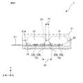
- FIG. 6A is a cross-sectional view of the capacitor module 1 of FIG. 1 taken along the line AA.
- FIG. 6B is an enlarged view of part of FIG. 6A.
- FIG. 6C is a BB cross-sectional view of the capacitor module 1 of FIG. 6D is a CC sectional view of the capacitor module 1 of FIG. 1.
- FIG. 7A is a perspective view showing the first projecting portion 22, the second projecting portion 23, and the support member 27 of the capacitor module 1 of FIG. 1.
- FIG. 7B is an enlarged view of a part of FIG. 7A.
- FIG. 8 is a perspective view showing sensor 31 of capacitor module 1 of FIG.
- the X, Y, and Z directions in the drawing indicate the horizontal direction, height direction, and vertical direction of the capacitor module 1, respectively.
- the capacitor module 1 includes six capacitors 11 to 16, a first busbar 21, a second busbar 26, a sensor 31, a case 51, and a sealing resin 52. Prepare.
- the capacitor module 1 accommodates the capacitors 11 to 16, part of the first bus bar 21, part of the second bus bar 26, and part of the sensor 31 in a case 51 made of resin. It is filled inside the case 51 .
- the first bus bar 21 and the second bus bar 26 are connected to the electrodes 11a-16a and 11b-16b of the six capacitors 11-16, respectively, as shown in FIG. External elements, circuits, or the like are connected to portions of the first bus bar 21 and the second bus bar 26 exposed from the case 51 .
- capacitors 11 to 13 in the first column correspond to the "first capacitor”
- the capacitors 14 to 16 in the second column correspond to the "second capacitor”.
- the capacitors 11-13 may be called first capacitors 11-13
- the capacitors 14-16 may be called second capacitors 14-16.
- the first capacitors 11 to 13 are film capacitors formed by winding a dielectric film. A dielectric film having a metal deposition film formed on the surface is wound and the wound body of the dielectric film is pressed into a flat shape. It is formed by The first capacitor 11, as shown in FIG. 4, has a first electrode 11a, a second electrode 11b, and a first side surface 11c connecting the first electrode 11a and the second electrode 11b. The first side surface 11c of the first capacitor 11 includes a pair of flat portions 11d and a pair of curved portions 11e. Similarly, the second capacitor 12 has a first electrode 12a, a second electrode 12b, and a first side surface 12c connecting the first electrode 12a and the second electrode 12b.
- the first side surface 12c of the first capacitor 12 includes a pair of flat portions 12d and a pair of curved portions 12e.
- the first capacitor 13 has a first electrode 13a, a second electrode 13b, and a first side surface 13c connecting the first electrode 13a and the second electrode 13b.
- the first side surface 13c of the first capacitor 13 includes a pair of flat portions 13d and a pair of curved portions 13e.
- dielectric films of the first capacitors 11 to 13 for example, plastic films such as polyethylene terephthalate, polypropylene, polyphenylene sulfide, or polyethylene naphthalate can be used. Moreover, Al, Zn, etc. can be used as a metal deposition film formed on the surface of a plastic film.
- the first electrodes 11a to 13a and the second electrodes 11b to 13b are formed by thermally spraying Zn or the like on the ends of the wound dielectric film.
- the first capacitor 11 and the first capacitor 12 are arranged such that the first electrode 11a and the first electrode 12a face each other. Also, the first capacitor 12 and the first capacitor 13 are arranged such that the second electrode 12b and the second electrode 13b face each other.
- the second capacitors 14 to 16 are film capacitors formed by winding a dielectric film. A dielectric film having a metal vapor deposition film formed on the surface is wound and the wound body of the dielectric film is pressed into a flat shape. It is formed by The second capacitors 14-16 have the same shape as the first capacitors 11-13, respectively.
- the second capacitor 14 has, as shown in FIG. 5, a third electrode 14a, a fourth electrode 14b, and a second side surface 14c connecting the third electrode 14a and the fourth electrode 14b.
- a second side surface 14c of the second capacitor 14 includes a pair of flat portions 14d and a pair of curved portions 14e.
- the second capacitor 15 has a third electrode 15a, a fourth electrode 15b, and a second side surface 15c connecting the third electrode 15a and the fourth electrode 15b.
- a second side surface 15c of the second capacitor 15 includes a pair of flat portions 15d and a pair of curved portions 15e.
- the second capacitor 16 has a third electrode 16a, a fourth electrode 16b, and a second side surface 16c connecting the third electrode 16a and the fourth electrode 16b.
- a second side surface 16c of the second capacitor 16 includes a pair of flat portions 16d and a pair of curved portions 16e.
- dielectric films of the second capacitors 14 to 16 for example, plastic films such as polyethylene terephthalate, polypropylene, polyphenylene sulfide, or polyethylene naphthalate can be used. Moreover, Al, Zn, etc. can be used as a metal deposition film formed on the surface of a plastic film.
- the third electrodes 14a to 16a and the fourth electrodes 14b to 14b are formed by thermally spraying Zn or the like on the ends of the wound dielectric film.
- the second capacitor 14 and the second capacitor 15 are arranged such that the respective third electrodes 14a and 15a face each other. Further, the second capacitor 15 and the second capacitor 16 are arranged such that the respective fourth electrodes 15b and 16b face each other.
- the first capacitors 11 to 13 and the second capacitors 14 to 16 are connected to a first bus bar 21, which will be described later, with the first side faces 11c to 13c and the second side faces 14c to 16c facing each other in the first direction (Z direction). It is arranged on the support surface 21a. That is, the first side surface 11c of the first capacitor 11 and the second side surface 14c of the second capacitor 14 are arranged on the support surface 21a in a state of facing each other in the first direction. Similarly, the first capacitor 12 and the second capacitor 15 are arranged on the support surface 21a with the first side surface 12c and the second side surface 15c facing each other in the first direction.
- the first capacitor 13 and the second capacitor 16 are arranged on the support surface 21a with the first side surface 13c and the second side surface 16c facing each other in the first direction.
- the first direction is the direction along the support surface 21a of the first busbar 21, and is the Z direction in the present embodiment.
- the curved portions 11e to 13e of the first side surfaces 11c to 13c and the curved portions 14e to 16e of the second side surfaces 14c to 16c are arranged to face each other in the first direction.
- the first bus bar 21 is a plate-like conductive member electrically connected to the first electrodes 11a-13a of the first capacitors 11-13 and the third electrodes 14a-16a of the second capacitors 14-16. .
- the first bus bar 21 and the first electrodes 11a-13a and the third electrodes 14a-16a are electrically connected by soldering conductive pins 41 to each, as shown in FIGS. 3 and 7A. .
- the second capacitors 14 and 15 and the sensor 31 are omitted in FIG. 7A.
- the first bus bar 21 has a support surface 21a that supports the first side surfaces 11c-13c of the first capacitors 11-13 and the second side surfaces 14c-16c of the second capacitors 14-16 (see FIG. 7A).
- insulating paper 43 is arranged on the support surface 21a of the first bus bar 21. As shown in FIG. The insulating paper 43 electrically insulates the electrodes 11 a to 16 a and 11 b to 16 b of the first capacitors 11 to 13 and the second capacitors 14 to 16 from the first bus bar 21 .
- each of the capacitors 11 and 14 faces the curved portion 11e of the first capacitor 11 and the curved portion 14e of the second capacitors 14 to 16.
- the flat portions 11d and 14d of are arranged to face the support surface 21a. That is, in the first capacitor 11 and the second capacitor 14, the flat portion 11d of the first side surface 11c and the flat portion 14d of the second side surface 14c face the support surface 21a, and the curved portions 11e and 14e are directed toward the support surface 21a. They are arranged to face each other in one direction (Z direction).
- the first capacitor 12 and the second capacitor 15 are configured such that the flat portion 12d of the first side surface 12c and the flat portion 15d of the second side surface 15c face the support surface 21a, and the curved portion 12e and curved portion 15e are arranged to face each other in the first direction (Z direction).
- the first capacitor 13 and the second capacitor 16 are configured such that the flat portion 13d of the first side surface 13c and the flat portion 16d of the second side surface 16c face the support surface 21a, and the curved portion 13e is formed. and the curved portion 16e are arranged to face each other in the first direction (Z direction).
- a space S1 is formed separating the portion 14e in the first direction (Z direction). That is, from the position where the distance between the curved portion 11e of the first side surface 11c and the curved portion 14e of the second side surface 14c is the shortest distance d1, the distance increases toward the support surface 21a of the first bus bar 21, and near the support surface 21a The distance is d2. Therefore, a space S1 is formed between the first capacitor 11 and the second capacitor .
- the elongated portion 33 of the sensor 31 which will be described later, has a position where the distance between the first side surface 11 c of the first capacitor 11 and the second side surface 14 c of the second capacitor 14 is the shortest distance (distance d ⁇ b>1 ), and a position where the first bus bar 21 is supported. It is arranged in the space S1 formed between the surface 21a and the surface 21a. That is, the elongated portion 33 of the sensor 31 is arranged in a portion (space S1) surrounded by the curved portion 11e of the first capacitor 11, the curved portion 14e of the second capacitor 14, and the support surface 21a.
- a space S1 is formed between the first capacitor 12 and the second capacitor 15 and between the first capacitor 13 and the second capacitor 16 as well.
- the first busbar 21 has a positioning portion 21b for positioning the elongated portion 33 (see FIG. 3) of the sensor 31, as shown in FIG. 7A.
- the positioning portion 21 b includes a first protrusion 22 and a second protrusion 23 .
- Both the first projecting portion 22 and the second projecting portion 23 are projecting portions projecting from the support surface 21a of the first bus bar 21 in the Y direction.
- the first projecting portion 22 and the second projecting portion 23 can be formed by, for example, press working.
- the insulating paper 43 arranged on the support surface 21a of the first bus bar 21 has holes through which the first projecting portion 22 and the second projecting portion 23 pass.
- a part of the first protrusion 22 protrudes from the support surface 21a to form a through hole 22a through which the elongated portion 33 of the sensor 31 is inserted.
- the first projecting portion 22 positions the elongated portion 33 in a radial direction perpendicular to the axial direction (X direction).
- the through hole 22 a is formed to have a diameter larger than the diameters of the detection portion 32 and the elongated portion 33 of the sensor 31 . In this case, the sensor 31 can be easily inserted into the through hole 22a, and damage to the sensor 31 can be suppressed.
- the through hole 22 a may be formed to have substantially the same size as the diameters of the detection portion 32 and the elongated portion 33 of the sensor 31 . In this case, the positioning accuracy of the sensor 31 can be improved.
- a part of the second protruding portion 23 protrudes from the support surface 21a and can abut against the detection portion 32 (see FIG. 3) of the elongated portion 33 in the axial direction of the elongated portion 33.
- the second projecting portion 23 positions the elongated portion 33 in the axial direction ( ⁇ X direction).
- the first projecting portion 22 and the second projecting portion 23 are arranged in the space S1 (see FIG. 6B), like the elongated portion 33 of the sensor 31.
- one first protrusion 22 is arranged in the space S1 between the first capacitor 11 and the second capacitor 14, and another first protrusion 22 and a second protrusion 23 are placed in the second capacitor. It is arranged in the space S1 between the first capacitor 12 and the second capacitor 15 .
- the second bus bar 26 is a plate-like conductive member electrically connected to the second electrodes 11b-13b of the first capacitors 11-13 and the fourth electrodes 14b-16b of the second capacitors 14-16.
- the second bus bar 26 and the second electrodes 11b-13b and the fourth electrodes 14b-16b are electrically connected by soldering conductive pins 42 to each, as shown in FIG.
- the second busbar 26 is arranged on the opposite side of the support surface 21a with respect to the first busbar 21 .
- insulating paper 44 is arranged between the first busbar 21 and the second busbar 26 to insulate the first busbar 21 and the second busbar 26 .
- a support member 27 is provided on the outer edge of the second busbar 26 .
- the support member 27 is a portion that abuts on the outer peripheral portion of the elongated portion 33 (see FIG. 3) of the sensor 31 .
- the support member 27 is provided on the second busbar 26 at a position that does not overlap the support surface 21 a of the first busbar 21 .
- the support member 27 can be formed by, for example, press working, similarly to the first projecting portion 22 and the second projecting portion 23 .
- a claw 27 a is formed on the support member 27 .
- the elongated portion 33 is positioned by hooking the elongated portion 33 on the claw 27 a and pressing the claw 27 a toward the second bus bar 26 . Therefore, the movement of the elongated portion 33 in the X direction can be suppressed.
- the support member 27 By providing the support member 27, when the elongated portion 33 engaged with the positioning portion 21b is pulled out of the case 51, it contacts the first electrode 11a of the first capacitor 11 or the third electrode 14a of the second capacitor 14. The position of the elongated portion 33 can be regulated so that it does not occur. In addition, by providing the support member 27 at a position of the second bus bar 26 that does not overlap with the support surface 21 a of the first bus bar 21 , the through hole in the insulating paper 43 is reduced compared to the case where the support member 27 is provided at a position that overlaps the support surface 21 a of the first bus bar 21 . is not required, and the configuration can be simplified. Also, the dimension in the Y direction can be shortened.
- the support member 27 can be formed by, for example, pressing.
- Sensor 31 is a sensor having a detection unit for detecting an abnormality in capacitor module 1 .
- Abnormalities related to the capacitor module 1 include, for example, overheating, overcurrent, or overvoltage.
- the sensor 31 is a temperature sensor that detects temperature.
- the sensor 31 has an elongated portion 33 with a detection portion 32 at its tip.
- the elongated portion 33 is a rod-shaped or linear portion.
- the sensor 31 also has a connecting portion 34 .
- a part of the detection part 32 and the elongated part 33 of the sensor 31 is arranged on the support surface 21a of the first bus bar 21, as shown in FIGS. 3 and 6A. Further, in the present embodiment, part of detection portion 32 and elongated portion 33 is inserted into through hole 22 a of first projecting portion 22 of first bus bar 21 . Therefore, the elongated portion 33 can be positioned in the radial direction (direction parallel to the YZ plane).
- the detection portion 32 which is the tip of the sensor 31, is in contact with the second projecting portion 23 in the X direction.
- part of the elongated portion 33 is restricted from moving in the -X direction by the second protruding portion 23 .
- the elongated portion 33 is positioned by being hooked on the support member 27 of the second bus bar 26 .
- the detection part 32 and the elongated part 33 of the sensor 31 are positioned by the first protrusion 22 , the second protrusion 23 and the support member 27 .
- the detection portion 32 of the sensor 31 is arranged near the center of the capacitor module 1 .
- the detection unit 32 is arranged between the first capacitor 12 and the second capacitor 15 arranged in the center. That is, the elongated portion 33 including the detection portion 32 of the sensor 31 is arranged in the space S1 between the curved portion 12e of the first capacitor 12 and the curved portion 15e of the second capacitor 15 . Therefore, the sensor 31 can be arranged by utilizing the dead space S1 inside the case 51 of the capacitor module 1 .
- the detection part 32 of the sensor 31 is arranged between the first capacitor 12 and the second capacitor 15 near the center of the capacitor module 1 . Therefore, the central temperature can be detected while utilizing the dead space. Therefore, the accuracy of abnormality detection can be improved. Moreover, by utilizing the dead space, the capacitor module 1 can be miniaturized without affecting the design of the capacitor module 1 .
- the detection portion 32 and a part of the elongated portion 33 of the sensor 31 are arranged on the support surface 21a of the first bus bar 21 with the insulating paper 43 interposed therebetween. Since the first bus bar 21 has high thermal conductivity, the heat generated from the capacitors 11 to 16 is transmitted through the insulating paper 43 and the first bus bar 21 and detected by the detector 32 of the sensor 31 .
- the sensor 31 detects the ambient temperature around the capacitors 11 to 16, and since it can also detect heat transfer via the insulating paper 43 and the first bus bar 21, the temperature detection accuracy of the sensor 31 is improved. can do.
- the capacitor module 1 includes first capacitors 11 to 13, second capacitors 14 to 16, a first busbar 21, a second busbar 26, and a sensor 31.
- the first capacitors 11 to 13 are wound bodies of dielectric films, and include first electrodes 11a to 13a, second electrodes 11b to 13b facing the first electrodes 11a to 13a, and first electrodes 11a to 13a. and first side surfaces 11c to 13c connecting the second electrodes 11b to 13b.
- the first side surfaces 11c to 13c have a pair of flat portions 11d to 13d and curved portions 11e to 13e connecting the flat portions 11d to 13d.
- the second capacitors 14 to 16 are wound bodies of dielectric films, and include third electrodes 14a to 16a, fourth electrodes 14b to 16b facing the third electrodes 14a to 16a, and third electrodes 14a to 16a. and second side surfaces 14c to 16c connecting the fourth electrodes 14b to 16b.
- the second side surfaces 14c to 16c have a pair of flat portions 14d to 16d and curved portions 14e to 16e connecting the flat portions 14d to 16d.
- the first bus bar 21 is configured such that the first side surfaces 11c to 13c of the first capacitors 11 to 13 and the second side surfaces 14c to 16c of the second capacitors 14 to 16 face each other in the first direction along the support surface 21a.
- the second bus bar 26 is electrically connected to the second electrodes 11b-13b of the first capacitors 11-13 and the fourth electrodes 14b-16b of the second capacitors 14-16.
- the sensor 31 has a detection section 32 for detecting an abnormality regarding the capacitor module 1 .
- the curved portions 11e to 13e of the first side surfaces 11c to 13c and the second side surfaces 14c are provided.
- a space S1 is formed separating the curved portions 14e to 16e of .about.16c in the first direction.
- the detection part 32 of the sensor 31 is arranged in the space S1.
- the senor 31 has an elongated portion 33 with a detection portion 32 provided at its tip, and the elongated portion 33 is arranged in the space S1.
- the detection section 32 can be arranged near the center of the capacitor module 1 . Therefore, the sensitivity of abnormality detection can be improved.
- the first busbar 21 also has a positioning portion 21b for positioning the elongated portion 33 on the support surface 21a.
- the positioning portion 21b has a first projecting portion 22 that protrudes from the support surface 21a and has a through hole 22a through which the elongated portion 33 is inserted.
- the elongated portion 33 of the sensor 31 can be radially positioned.
- the positioning portion 21b has a second projecting portion 23 that protrudes from the support surface 21a and can come into contact with the detecting portion 32 of the elongated portion 33 in the axial direction of the elongated portion 33. As shown in FIG.
- Such a configuration allows the elongated portion 33 of the sensor 31 to be axially and radially positioned.
- the second bus bar 26 has a support member 27 that supports the elongated portion 33 .
- Second bus bar 26 is arranged on the opposite side of supporting surface 21 a of first bus bar 21 with respect to first bus bar 21 . It is provided in a position that does not overlap.
- the elongated portion 33 of the sensor 31 can be positioned while utilizing the dead space, which contributes to miniaturization of the capacitor module 1.
- the first capacitors 11 to 13 and the second capacitors 14 to 16 have flat portions 11d to 13d of the first side surfaces 11c to 13c and flat portions 14d to 16d of the second side surfaces 14c to 16c facing the support surface 21a. while the curved portions 11e to 16e are arranged to face each other in the first direction.
- a space S1 is formed in the portion where the curved portions 11e to 13e and the curved portions 14e to 16e face each other, and the sensor 31 can be arranged in the space S1. Therefore, the size of the capacitor module can be reduced without affecting the design of the capacitor module 1 .
- the senor 31 is a temperature sensor
- the detection section 32 is a heat sensitive section for detecting temperature.
- the capacitor module 1 includes the six capacitors 11 to 16 has been described, but the number of capacitors is not limited to this, and may be two or more.
- first protrusions 22 may be one or more.
- first projecting portion 22 and the second projecting portion 23 may not be arranged.
- the support member 27 may be formed on either the first bus bar or the second bus bar. That is, the first busbar 21 or the second busbar 26 may have a support member 27 that abuts on the outer peripheral portion of the elongated portion 33 so as to press the elongated portion 33 toward the first busbar 21 or the second busbar 26 . .
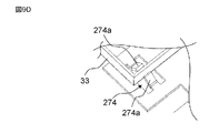
- FIG. 9A to 9E are partial enlarged views showing modifications of the support member 27.
- the support member 271 in FIG. 9A has arched claws 271a.
- the elongated portion 33 can be positioned by passing the elongated portion 33 through the claw 271a and pressing the claw 271a.
- the support member 272 in FIG. 9B is provided with two arch-shaped claws 272a. By providing two claws 272a, the positioning accuracy can be further improved.
- the support member 273 in FIG. 9C is formed in a plate shape with a bent claw 273a.
- the claw 273a may have such a shape instead of an arch shape.
- FIGS. 9A to 9C have arched claws 271a to 273a, but in the modification of FIGS.
- the support member 274 of FIG. 9D is provided with two claws 274a so as to sandwich the elongated portion 33 therebetween.
- the elongated portion 33 can be fitted from above, the arrangement of the sensor 31 is facilitated.
- the support member 275 of FIG. 9E is provided with three claws 275a so as to sandwich the elongated portion 33 therebetween. Positioning accuracy can be improved while facilitating the arrangement of the sensor 31 .
- FIG. 10 is a perspective view of the capacitor module 2 according to the second embodiment.
- FIG. 11A is a view of the capacitor module 2 of FIG. 10 viewed from the X direction.
- FIG. 11B is a partially enlarged view of FIG. 11A.
- 12 is a plan view of the capacitor module 2 of FIG. 10.
- the sensor 31 is omitted in FIG.
- FIGS. 11A and 11B the case 511 and the sealing resin 521 are omitted.
- the case 511, the sealing resin 521, and the capacitors 112 and 113 are omitted.
- the second embodiment differs from the first embodiment mainly in the arrangement of capacitors. Specifically, as shown in FIGS. 10 and 11, the capacitors 111 to 115 are arranged such that the curved portions 111e to 115e (see FIG. 11) rather than the flat portions 111d to 115d face the support surface 211a of the first bus bar 211. is different from the first embodiment.
- the capacitors 111 to 120 are arranged in 5 ⁇ 2 rows.
- the capacitors 111 to 115 are arranged such that the flat portions 111d to 115d (see FIG. 11) of the adjacent capacitors 111 to 115 face each other in the first direction (Y direction).
- the respective capacitors 111 to 115 are arranged such that the curved portions 111e to 115e face the supporting surface 211a of the first bus bar 211. As shown in FIG.
- the capacitor 112 corresponds to the "first capacitor” and the capacitor 113 corresponds to the "second capacitor” in the present embodiment.
- FIGS. 11A and 11B between the first side surface 112c of the first capacitor 112 and the second side surface 113c of the second capacitor 113, there is a curved portion 112e of the first side surface 112c and a curved portion 112e of the second side surface 113c.
- a space S2 is formed separating the portion 113e in the first direction (Y direction). That is, the distance between the first side surface 112c and the second side surface 113c increases from the shortest distance d3 toward the support surface 211a of the first bus bar 211, and reaches the distance d4 near the support surface 211a. Therefore, a space S2 is formed between the first capacitor 112 and the second capacitor 113 .
- the elongated portion 33 of the sensor 31 is located at a position where the distance between the first side surface 112c of the first capacitor 112 and the second side surface 113c of the second capacitor 113 is the shortest distance (distance d3) and the support surface 211a of the first bus bar 211. and the space S2 formed between. That is, the elongated portion 33 of the sensor is arranged in a portion (space S2) surrounded by the curved portion 112e of the first capacitor 112, the curved portion 113e of the second capacitor 113, and the support surface 211a.
- the first direction is the direction along the support surface 211a of the first bus bar 211, and is the Y direction in this embodiment.
- the first protrusion and/or the second protrusion may be formed in the space S2.
- the elongated portion 33 including the detection portion 32 of the sensor 31 is arranged on the supporting surface 211a of the first busbar 211. As shown in FIG. In the present embodiment, the elongated portion 33 of the sensor 31 is arranged between the first capacitor 112 and the second capacitor 113, but the arrangement position of the sensor is not limited to this. may be placed between
- the present invention is useful for capacitors used in various electronic devices, electrical devices, industrial devices, vehicle devices, and the like.
Landscapes
- Engineering & Computer Science (AREA)
- Power Engineering (AREA)
- Microelectronics & Electronic Packaging (AREA)
- Manufacturing & Machinery (AREA)
- Fixed Capacitors And Capacitor Manufacturing Machines (AREA)
Priority Applications (3)
| Application Number | Priority Date | Filing Date | Title |
|---|---|---|---|
| JP2023505204A JP7546753B2 (ja) | 2021-03-12 | 2022-01-31 | コンデンサモジュール |
| CN202280019896.0A CN117015837A (zh) | 2021-03-12 | 2022-01-31 | 电容器模块 |
| US18/461,795 US20230420185A1 (en) | 2021-03-12 | 2023-09-06 | Capacitor module |
Applications Claiming Priority (2)
| Application Number | Priority Date | Filing Date | Title |
|---|---|---|---|
| JP2021040324 | 2021-03-12 | ||
| JP2021-040324 | 2021-03-12 |
Related Child Applications (1)
| Application Number | Title | Priority Date | Filing Date |
|---|---|---|---|
| US18/461,795 Continuation US20230420185A1 (en) | 2021-03-12 | 2023-09-06 | Capacitor module |
Publications (1)
| Publication Number | Publication Date |
|---|---|
| WO2022190708A1 true WO2022190708A1 (ja) | 2022-09-15 |
Family
ID=83226681
Family Applications (1)
| Application Number | Title | Priority Date | Filing Date |
|---|---|---|---|
| PCT/JP2022/003632 Ceased WO2022190708A1 (ja) | 2021-03-12 | 2022-01-31 | コンデンサモジュール |
Country Status (4)
| Country | Link |
|---|---|
| US (1) | US20230420185A1 (https=) |
| JP (1) | JP7546753B2 (https=) |
| CN (1) | CN117015837A (https=) |
| WO (1) | WO2022190708A1 (https=) |
Cited By (2)
| Publication number | Priority date | Publication date | Assignee | Title |
|---|---|---|---|---|
| US20240222008A1 (en) * | 2021-05-10 | 2024-07-04 | Mitsubishi Electric Corpotation | Capacitor unit and electronic device |
| WO2025132097A1 (fr) * | 2023-12-20 | 2025-06-26 | Valeo Eautomotive Germany Gmbh | Dispositif comprenant un condensateur de liaison à courant continu, méthode de fabrication correspondante et onduleur |
Citations (5)
| Publication number | Priority date | Publication date | Assignee | Title |
|---|---|---|---|---|
| JP2003087941A (ja) * | 2001-09-05 | 2003-03-20 | Auto Network Gijutsu Kenkyusho:Kk | 電気接続箱 |
| JP2009111370A (ja) * | 2007-10-10 | 2009-05-21 | Panasonic Corp | ケースモールド型コンデンサ |
| US20130050878A1 (en) * | 2011-08-26 | 2013-02-28 | Schneider Electric USA, Inc. | Differential temperature monitoring of electrical devices |
| JP2014170882A (ja) * | 2013-03-05 | 2014-09-18 | Shizuki Electric Co Inc | コンデンサ |
| JP2020136428A (ja) * | 2019-02-18 | 2020-08-31 | 株式会社指月電機製作所 | コンデンサ |
Family Cites Families (1)
| Publication number | Priority date | Publication date | Assignee | Title |
|---|---|---|---|---|
| CN109155195B (zh) | 2016-05-25 | 2020-10-30 | 松下知识产权经营株式会社 | 电容器 |
-
2022
- 2022-01-31 WO PCT/JP2022/003632 patent/WO2022190708A1/ja not_active Ceased
- 2022-01-31 JP JP2023505204A patent/JP7546753B2/ja active Active
- 2022-01-31 CN CN202280019896.0A patent/CN117015837A/zh active Pending
-
2023
- 2023-09-06 US US18/461,795 patent/US20230420185A1/en active Pending
Patent Citations (5)
| Publication number | Priority date | Publication date | Assignee | Title |
|---|---|---|---|---|
| JP2003087941A (ja) * | 2001-09-05 | 2003-03-20 | Auto Network Gijutsu Kenkyusho:Kk | 電気接続箱 |
| JP2009111370A (ja) * | 2007-10-10 | 2009-05-21 | Panasonic Corp | ケースモールド型コンデンサ |
| US20130050878A1 (en) * | 2011-08-26 | 2013-02-28 | Schneider Electric USA, Inc. | Differential temperature monitoring of electrical devices |
| JP2014170882A (ja) * | 2013-03-05 | 2014-09-18 | Shizuki Electric Co Inc | コンデンサ |
| JP2020136428A (ja) * | 2019-02-18 | 2020-08-31 | 株式会社指月電機製作所 | コンデンサ |
Cited By (3)
| Publication number | Priority date | Publication date | Assignee | Title |
|---|---|---|---|---|
| US20240222008A1 (en) * | 2021-05-10 | 2024-07-04 | Mitsubishi Electric Corpotation | Capacitor unit and electronic device |
| WO2025132097A1 (fr) * | 2023-12-20 | 2025-06-26 | Valeo Eautomotive Germany Gmbh | Dispositif comprenant un condensateur de liaison à courant continu, méthode de fabrication correspondante et onduleur |
| FR3157651A1 (fr) * | 2023-12-20 | 2025-06-27 | Valeo Eautomotive Germany Gmbh | Dispositif comprenant un condensateur de liaison à courant continu, méthode de fabrication correspondante et onduleur |
Also Published As
| Publication number | Publication date |
|---|---|
| JPWO2022190708A1 (https=) | 2022-09-15 |
| CN117015837A (zh) | 2023-11-07 |
| JP7546753B2 (ja) | 2024-09-06 |
| US20230420185A1 (en) | 2023-12-28 |
Similar Documents
| Publication | Publication Date | Title |
|---|---|---|
| US10847776B2 (en) | Conductive module and battery pack | |
| US9739671B2 (en) | Pressing force sensor | |
| CN111133286A (zh) | 传感器单元及蓄电模块 | |
| JP6247448B2 (ja) | 電源装置 | |
| KR102948189B1 (ko) | 차량의 배터리팩 | |
| WO2022190708A1 (ja) | コンデンサモジュール | |
| JP2016090286A (ja) | 温度検出体の取付構造 | |
| EP3605649B1 (en) | Battery pack protection element attachment tab, battery pack parallel fixing component, and battery pack | |
| JP7259993B2 (ja) | 配線モジュール、および、蓄電モジュール | |
| WO2022196319A1 (ja) | 配線モジュール | |
| JP7177109B2 (ja) | 導電モジュール | |
| US20200365865A1 (en) | Bus Bar Module | |
| JP6213203B2 (ja) | 組電池 | |
| US11876249B2 (en) | Conductive module | |
| US20250149748A1 (en) | Connection module set, electrode connection member set, and battery pack | |
| US20240274904A1 (en) | Sensor unit and sensor unit-equipped battery wiring module | |
| JP6610007B2 (ja) | 電池パック | |
| US20230170583A1 (en) | Battery module having a laminated busbar assembly | |
| US20260121244A1 (en) | Battery module having a laminated busbar assembly | |
| US20250149760A1 (en) | Wiring module and battery pack | |
| US20250149723A1 (en) | Wiring module and battery pack | |
| JP7697074B2 (ja) | 温度検出構造を備えた電池モジュール | |
| JP2009231003A (ja) | 温度検出モジュール | |
| JP2025180148A (ja) | 電気接続ユニット | |
| JP4957575B2 (ja) | 半導体素子の絶縁構造および電気機器 |
Legal Events
| Date | Code | Title | Description |
|---|---|---|---|
| 121 | Ep: the epo has been informed by wipo that ep was designated in this application |
Ref document number: 22766675 Country of ref document: EP Kind code of ref document: A1 |
|
| WWE | Wipo information: entry into national phase |
Ref document number: 202280019896.0 Country of ref document: CN |
|
| WWE | Wipo information: entry into national phase |
Ref document number: 2023505204 Country of ref document: JP |
|
| NENP | Non-entry into the national phase |
Ref country code: DE |
|
| 122 | Ep: pct application non-entry in european phase |
Ref document number: 22766675 Country of ref document: EP Kind code of ref document: A1 |