WO2022186004A1 - Substrate with multilayer reflective film, reflective mask blank, reflective mask, and method for manufacturing semiconductor device - Google Patents
Substrate with multilayer reflective film, reflective mask blank, reflective mask, and method for manufacturing semiconductor device Download PDFInfo
- Publication number
- WO2022186004A1 WO2022186004A1 PCT/JP2022/007287 JP2022007287W WO2022186004A1 WO 2022186004 A1 WO2022186004 A1 WO 2022186004A1 JP 2022007287 W JP2022007287 W JP 2022007287W WO 2022186004 A1 WO2022186004 A1 WO 2022186004A1
- Authority
- WO
- WIPO (PCT)
- Prior art keywords
- film
- multilayer reflective
- substrate
- material layer
- reflective film
- Prior art date
Links
- 239000000758 substrate Substances 0.000 title claims abstract description 113
- 238000000034 method Methods 0.000 title claims abstract description 34
- 239000004065 semiconductor Substances 0.000 title claims abstract description 21
- 238000004519 manufacturing process Methods 0.000 title claims abstract description 18
- 239000000463 material Substances 0.000 claims abstract description 139
- 230000001681 protective effect Effects 0.000 claims abstract description 56
- 229910052751 metal Inorganic materials 0.000 claims abstract description 43
- 239000002184 metal Substances 0.000 claims abstract description 42
- 229910052710 silicon Inorganic materials 0.000 claims abstract description 28
- 239000011777 magnesium Substances 0.000 claims abstract description 25
- 239000010936 titanium Substances 0.000 claims abstract description 24
- IJGRMHOSHXDMSA-UHFFFAOYSA-N Atomic nitrogen Chemical compound N#N IJGRMHOSHXDMSA-UHFFFAOYSA-N 0.000 claims abstract description 20
- 239000010703 silicon Substances 0.000 claims abstract description 19
- 229910052727 yttrium Inorganic materials 0.000 claims abstract description 19
- XUIMIQQOPSSXEZ-UHFFFAOYSA-N Silicon Chemical compound [Si] XUIMIQQOPSSXEZ-UHFFFAOYSA-N 0.000 claims abstract description 18
- 229910052757 nitrogen Inorganic materials 0.000 claims abstract description 16
- 229910052782 aluminium Inorganic materials 0.000 claims abstract description 15
- 229910052799 carbon Inorganic materials 0.000 claims abstract description 14
- 229910052749 magnesium Inorganic materials 0.000 claims abstract description 14
- 229910052719 titanium Inorganic materials 0.000 claims abstract description 14
- FYYHWMGAXLPEAU-UHFFFAOYSA-N Magnesium Chemical compound [Mg] FYYHWMGAXLPEAU-UHFFFAOYSA-N 0.000 claims abstract description 11
- XAGFODPZIPBFFR-UHFFFAOYSA-N aluminium Chemical compound [Al] XAGFODPZIPBFFR-UHFFFAOYSA-N 0.000 claims abstract description 11
- VSZWPYCFIRKVQL-UHFFFAOYSA-N selanylidenegallium;selenium Chemical compound [Se].[Se]=[Ga].[Se]=[Ga] VSZWPYCFIRKVQL-UHFFFAOYSA-N 0.000 claims abstract description 11
- RTAQQCXQSZGOHL-UHFFFAOYSA-N Titanium Chemical compound [Ti] RTAQQCXQSZGOHL-UHFFFAOYSA-N 0.000 claims abstract description 10
- VWQVUPCCIRVNHF-UHFFFAOYSA-N yttrium atom Chemical compound [Y] VWQVUPCCIRVNHF-UHFFFAOYSA-N 0.000 claims abstract description 10
- OKTJSMMVPCPJKN-UHFFFAOYSA-N Carbon Chemical compound [C] OKTJSMMVPCPJKN-UHFFFAOYSA-N 0.000 claims abstract description 9
- 239000006096 absorbing agent Substances 0.000 claims description 74
- 238000012546 transfer Methods 0.000 claims description 20
- 229910044991 metal oxide Inorganic materials 0.000 claims description 13
- 150000004706 metal oxides Chemical class 0.000 claims description 13
- 229910052726 zirconium Inorganic materials 0.000 claims description 10
- 230000008569 process Effects 0.000 claims description 7
- 238000001459 lithography Methods 0.000 claims description 3
- 238000000059 patterning Methods 0.000 claims description 2
- 230000015572 biosynthetic process Effects 0.000 abstract description 14
- 229910021332 silicide Inorganic materials 0.000 abstract description 12
- 230000009467 reduction Effects 0.000 abstract description 9
- FVBUAEGBCNSCDD-UHFFFAOYSA-N silicide(4-) Chemical compound [Si-4] FVBUAEGBCNSCDD-UHFFFAOYSA-N 0.000 abstract description 9
- 238000002310 reflectometry Methods 0.000 abstract 1
- 239000010408 film Substances 0.000 description 352
- 239000010410 layer Substances 0.000 description 178
- HBMJWWWQQXIZIP-UHFFFAOYSA-N silicon carbide Chemical compound [Si+]#[C-] HBMJWWWQQXIZIP-UHFFFAOYSA-N 0.000 description 41
- 229910010271 silicon carbide Inorganic materials 0.000 description 40
- 239000011241 protective layer Substances 0.000 description 34
- 238000005530 etching Methods 0.000 description 26
- 229910004298 SiO 2 Inorganic materials 0.000 description 21
- 150000001875 compounds Chemical class 0.000 description 20
- 239000007789 gas Substances 0.000 description 20
- 229910052760 oxygen Inorganic materials 0.000 description 18
- 239000011651 chromium Substances 0.000 description 16
- 238000010438 heat treatment Methods 0.000 description 15
- 229910052796 boron Inorganic materials 0.000 description 13
- QVGXLLKOCUKJST-UHFFFAOYSA-N atomic oxygen Chemical compound [O] QVGXLLKOCUKJST-UHFFFAOYSA-N 0.000 description 12
- 230000003287 optical effect Effects 0.000 description 12
- 239000001301 oxygen Substances 0.000 description 12
- 229910052715 tantalum Inorganic materials 0.000 description 12
- 229910052804 chromium Inorganic materials 0.000 description 10
- 238000001755 magnetron sputter deposition Methods 0.000 description 10
- 150000002739 metals Chemical class 0.000 description 10
- 239000012298 atmosphere Substances 0.000 description 9
- 239000000460 chlorine Substances 0.000 description 9
- 230000000052 comparative effect Effects 0.000 description 9
- 238000001659 ion-beam spectroscopy Methods 0.000 description 9
- 239000010955 niobium Substances 0.000 description 9
- 230000000737 periodic effect Effects 0.000 description 9
- 239000010948 rhodium Substances 0.000 description 9
- 229910052707 ruthenium Inorganic materials 0.000 description 9
- 238000005245 sintering Methods 0.000 description 9
- VYZAMTAEIAYCRO-UHFFFAOYSA-N Chromium Chemical compound [Cr] VYZAMTAEIAYCRO-UHFFFAOYSA-N 0.000 description 7
- 229910045601 alloy Inorganic materials 0.000 description 7
- 239000000956 alloy Substances 0.000 description 7
- 229910052750 molybdenum Inorganic materials 0.000 description 7
- 229910052703 rhodium Inorganic materials 0.000 description 7
- ZAMOUSCENKQFHK-UHFFFAOYSA-N Chlorine atom Chemical compound [Cl] ZAMOUSCENKQFHK-UHFFFAOYSA-N 0.000 description 6
- 229910052801 chlorine Inorganic materials 0.000 description 6
- 230000010363 phase shift Effects 0.000 description 6
- BASFCYQUMIYNBI-UHFFFAOYSA-N platinum Substances [Pt] BASFCYQUMIYNBI-UHFFFAOYSA-N 0.000 description 6
- GUVRBAGPIYLISA-UHFFFAOYSA-N tantalum atom Chemical compound [Ta] GUVRBAGPIYLISA-UHFFFAOYSA-N 0.000 description 6
- YCKRFDGAMUMZLT-UHFFFAOYSA-N Fluorine atom Chemical compound [F] YCKRFDGAMUMZLT-UHFFFAOYSA-N 0.000 description 5
- VYPSYNLAJGMNEJ-UHFFFAOYSA-N Silicium dioxide Chemical compound O=[Si]=O VYPSYNLAJGMNEJ-UHFFFAOYSA-N 0.000 description 5
- 230000007547 defect Effects 0.000 description 5
- 238000010586 diagram Methods 0.000 description 5
- 239000011737 fluorine Substances 0.000 description 5
- 229910052731 fluorine Inorganic materials 0.000 description 5
- 229910052758 niobium Inorganic materials 0.000 description 5
- 150000003377 silicon compounds Chemical class 0.000 description 5
- 239000002344 surface layer Substances 0.000 description 5
- ZOXJGFHDIHLPTG-UHFFFAOYSA-N Boron Chemical compound [B] ZOXJGFHDIHLPTG-UHFFFAOYSA-N 0.000 description 4
- 238000004833 X-ray photoelectron spectroscopy Methods 0.000 description 4
- 238000005229 chemical vapour deposition Methods 0.000 description 4
- 238000009792 diffusion process Methods 0.000 description 4
- 238000001312 dry etching Methods 0.000 description 4
- 229910052739 hydrogen Inorganic materials 0.000 description 4
- PXHVJJICTQNCMI-UHFFFAOYSA-N nickel Substances [Ni] PXHVJJICTQNCMI-UHFFFAOYSA-N 0.000 description 4
- KDLHZDBZIXYQEI-UHFFFAOYSA-N palladium Substances [Pd] KDLHZDBZIXYQEI-UHFFFAOYSA-N 0.000 description 4
- 229910052697 platinum Inorganic materials 0.000 description 4
- 238000007517 polishing process Methods 0.000 description 4
- 239000002356 single layer Substances 0.000 description 4
- KJTLSVCANCCWHF-UHFFFAOYSA-N Ruthenium Chemical compound [Ru] KJTLSVCANCCWHF-UHFFFAOYSA-N 0.000 description 3
- 229910052581 Si3N4 Inorganic materials 0.000 description 3
- 230000000903 blocking effect Effects 0.000 description 3
- 230000008859 change Effects 0.000 description 3
- 238000004140 cleaning Methods 0.000 description 3
- 239000010949 copper Substances 0.000 description 3
- 230000007423 decrease Effects 0.000 description 3
- 238000010894 electron beam technology Methods 0.000 description 3
- 229910052732 germanium Inorganic materials 0.000 description 3
- 239000011521 glass Substances 0.000 description 3
- 239000000203 mixture Substances 0.000 description 3
- 238000005546 reactive sputtering Methods 0.000 description 3
- -1 silicon nitrides Chemical class 0.000 description 3
- 230000003746 surface roughness Effects 0.000 description 3
- 150000003482 tantalum compounds Chemical class 0.000 description 3
- 239000010409 thin film Substances 0.000 description 3
- 229910052721 tungsten Inorganic materials 0.000 description 3
- XKRFYHLGVUSROY-UHFFFAOYSA-N Argon Chemical compound [Ar] XKRFYHLGVUSROY-UHFFFAOYSA-N 0.000 description 2
- UFHFLCQGNIYNRP-UHFFFAOYSA-N Hydrogen Chemical compound [H][H] UFHFLCQGNIYNRP-UHFFFAOYSA-N 0.000 description 2
- 229910010413 TiO 2 Inorganic materials 0.000 description 2
- GWEVSGVZZGPLCZ-UHFFFAOYSA-N Titan oxide Chemical compound O=[Ti]=O GWEVSGVZZGPLCZ-UHFFFAOYSA-N 0.000 description 2
- MCMNRKCIXSYSNV-UHFFFAOYSA-N Zirconium dioxide Chemical compound O=[Zr]=O MCMNRKCIXSYSNV-UHFFFAOYSA-N 0.000 description 2
- 238000000137 annealing Methods 0.000 description 2
- 239000003795 chemical substances by application Substances 0.000 description 2
- 150000001845 chromium compounds Chemical class 0.000 description 2
- 229910052681 coesite Inorganic materials 0.000 description 2
- 229910052802 copper Inorganic materials 0.000 description 2
- 229910052906 cristobalite Inorganic materials 0.000 description 2
- 238000000151 deposition Methods 0.000 description 2
- 230000002542 deteriorative effect Effects 0.000 description 2
- 230000000694 effects Effects 0.000 description 2
- GNPVGFCGXDBREM-UHFFFAOYSA-N germanium atom Chemical compound [Ge] GNPVGFCGXDBREM-UHFFFAOYSA-N 0.000 description 2
- 239000010931 gold Substances 0.000 description 2
- 229910052735 hafnium Inorganic materials 0.000 description 2
- VBJZVLUMGGDVMO-UHFFFAOYSA-N hafnium atom Chemical compound [Hf] VBJZVLUMGGDVMO-UHFFFAOYSA-N 0.000 description 2
- 238000007689 inspection Methods 0.000 description 2
- 239000011572 manganese Substances 0.000 description 2
- 229910052759 nickel Inorganic materials 0.000 description 2
- GUCVJGMIXFAOAE-UHFFFAOYSA-N niobium atom Chemical compound [Nb] GUCVJGMIXFAOAE-UHFFFAOYSA-N 0.000 description 2
- 230000003647 oxidation Effects 0.000 description 2
- 238000007254 oxidation reaction Methods 0.000 description 2
- 229910052763 palladium Inorganic materials 0.000 description 2
- 239000012466 permeate Substances 0.000 description 2
- 238000005240 physical vapour deposition Methods 0.000 description 2
- MHOVAHRLVXNVSD-UHFFFAOYSA-N rhodium atom Chemical compound [Rh] MHOVAHRLVXNVSD-UHFFFAOYSA-N 0.000 description 2
- 238000001004 secondary ion mass spectrometry Methods 0.000 description 2
- 239000000377 silicon dioxide Substances 0.000 description 2
- 235000012239 silicon dioxide Nutrition 0.000 description 2
- HQVNEWCFYHHQES-UHFFFAOYSA-N silicon nitride Chemical compound N12[Si]34N5[Si]62N3[Si]51N64 HQVNEWCFYHHQES-UHFFFAOYSA-N 0.000 description 2
- 229910052814 silicon oxide Inorganic materials 0.000 description 2
- 229910052682 stishovite Inorganic materials 0.000 description 2
- 230000001629 suppression Effects 0.000 description 2
- 229910052905 tridymite Inorganic materials 0.000 description 2
- WFKWXMTUELFFGS-UHFFFAOYSA-N tungsten Chemical compound [W] WFKWXMTUELFFGS-UHFFFAOYSA-N 0.000 description 2
- 239000010937 tungsten Substances 0.000 description 2
- 238000001771 vacuum deposition Methods 0.000 description 2
- LEONUFNNVUYDNQ-UHFFFAOYSA-N vanadium atom Chemical compound [V] LEONUFNNVUYDNQ-UHFFFAOYSA-N 0.000 description 2
- 101150013999 CRBN gene Proteins 0.000 description 1
- RYGMFSIKBFXOCR-UHFFFAOYSA-N Copper Chemical compound [Cu] RYGMFSIKBFXOCR-UHFFFAOYSA-N 0.000 description 1
- XPDWGBQVDMORPB-UHFFFAOYSA-N Fluoroform Chemical compound FC(F)F XPDWGBQVDMORPB-UHFFFAOYSA-N 0.000 description 1
- XEEYBQQBJWHFJM-UHFFFAOYSA-N Iron Chemical compound [Fe] XEEYBQQBJWHFJM-UHFFFAOYSA-N 0.000 description 1
- PWHULOQIROXLJO-UHFFFAOYSA-N Manganese Chemical compound [Mn] PWHULOQIROXLJO-UHFFFAOYSA-N 0.000 description 1
- ZOKXTWBITQBERF-UHFFFAOYSA-N Molybdenum Chemical compound [Mo] ZOKXTWBITQBERF-UHFFFAOYSA-N 0.000 description 1
- 229910019887 RuMo Inorganic materials 0.000 description 1
- 229910003902 SiCl 4 Inorganic materials 0.000 description 1
- 229910004541 SiN Inorganic materials 0.000 description 1
- BQCADISMDOOEFD-UHFFFAOYSA-N Silver Chemical compound [Ag] BQCADISMDOOEFD-UHFFFAOYSA-N 0.000 description 1
- 229910001362 Ta alloys Inorganic materials 0.000 description 1
- 229910004535 TaBN Inorganic materials 0.000 description 1
- 229910004162 TaHf Inorganic materials 0.000 description 1
- 229910003071 TaON Inorganic materials 0.000 description 1
- 229910004200 TaSiN Inorganic materials 0.000 description 1
- ATJFFYVFTNAWJD-UHFFFAOYSA-N Tin Chemical compound [Sn] ATJFFYVFTNAWJD-UHFFFAOYSA-N 0.000 description 1
- 238000010521 absorption reaction Methods 0.000 description 1
- 230000002378 acidificating effect Effects 0.000 description 1
- 230000002411 adverse Effects 0.000 description 1
- PNEYBMLMFCGWSK-UHFFFAOYSA-N aluminium oxide Inorganic materials [O-2].[O-2].[O-2].[Al+3].[Al+3] PNEYBMLMFCGWSK-UHFFFAOYSA-N 0.000 description 1
- 239000007864 aqueous solution Substances 0.000 description 1
- 229910052786 argon Inorganic materials 0.000 description 1
- 230000008033 biological extinction Effects 0.000 description 1
- 229910017052 cobalt Inorganic materials 0.000 description 1
- 239000010941 cobalt Substances 0.000 description 1
- GUTLYIVDDKVIGB-UHFFFAOYSA-N cobalt atom Chemical compound [Co] GUTLYIVDDKVIGB-UHFFFAOYSA-N 0.000 description 1
- 238000011109 contamination Methods 0.000 description 1
- 238000012937 correction Methods 0.000 description 1
- 229910052593 corundum Inorganic materials 0.000 description 1
- 230000008021 deposition Effects 0.000 description 1
- RWRIWBAIICGTTQ-UHFFFAOYSA-N difluoromethane Chemical compound FCF RWRIWBAIICGTTQ-UHFFFAOYSA-N 0.000 description 1
- 238000005516 engineering process Methods 0.000 description 1
- 238000011156 evaluation Methods 0.000 description 1
- 238000001900 extreme ultraviolet lithography Methods 0.000 description 1
- NBVXSUQYWXRMNV-UHFFFAOYSA-N fluoromethane Chemical compound FC NBVXSUQYWXRMNV-UHFFFAOYSA-N 0.000 description 1
- 239000002241 glass-ceramic Substances 0.000 description 1
- PCHJSUWPFVWCPO-UHFFFAOYSA-N gold Chemical compound [Au] PCHJSUWPFVWCPO-UHFFFAOYSA-N 0.000 description 1
- 229910052737 gold Inorganic materials 0.000 description 1
- 239000011261 inert gas Substances 0.000 description 1
- 229910052741 iridium Inorganic materials 0.000 description 1
- GKOZUEZYRPOHIO-UHFFFAOYSA-N iridium atom Chemical compound [Ir] GKOZUEZYRPOHIO-UHFFFAOYSA-N 0.000 description 1
- 229910052743 krypton Inorganic materials 0.000 description 1
- DNNSSWSSYDEUBZ-UHFFFAOYSA-N krypton atom Chemical compound [Kr] DNNSSWSSYDEUBZ-UHFFFAOYSA-N 0.000 description 1
- 238000010030 laminating Methods 0.000 description 1
- 229910052746 lanthanum Inorganic materials 0.000 description 1
- 229910052748 manganese Inorganic materials 0.000 description 1
- 230000005012 migration Effects 0.000 description 1
- 238000013508 migration Methods 0.000 description 1
- 239000011733 molybdenum Substances 0.000 description 1
- 150000004767 nitrides Chemical class 0.000 description 1
- 239000012299 nitrogen atmosphere Substances 0.000 description 1
- QYSGYZVSCZSLHT-UHFFFAOYSA-N octafluoropropane Chemical compound FC(F)(F)C(F)(F)C(F)(F)F QYSGYZVSCZSLHT-UHFFFAOYSA-N 0.000 description 1
- 101150016677 ohgt gene Proteins 0.000 description 1
- 238000002360 preparation method Methods 0.000 description 1
- 238000001552 radio frequency sputter deposition Methods 0.000 description 1
- 230000035945 sensitivity Effects 0.000 description 1
- 229910052709 silver Inorganic materials 0.000 description 1
- 239000004332 silver Substances 0.000 description 1
- 238000009751 slip forming Methods 0.000 description 1
- 238000004544 sputter deposition Methods 0.000 description 1
- 239000000126 substance Substances 0.000 description 1
- SFZCNBIFKDRMGX-UHFFFAOYSA-N sulfur hexafluoride Chemical compound FS(F)(F)(F)(F)F SFZCNBIFKDRMGX-UHFFFAOYSA-N 0.000 description 1
- JBQYATWDVHIOAR-UHFFFAOYSA-N tellanylidenegermanium Chemical compound [Te]=[Ge] JBQYATWDVHIOAR-UHFFFAOYSA-N 0.000 description 1
- 229910052714 tellurium Inorganic materials 0.000 description 1
- PORWMNRCUJJQNO-UHFFFAOYSA-N tellurium atom Chemical compound [Te] PORWMNRCUJJQNO-UHFFFAOYSA-N 0.000 description 1
- 229910001845 yogo sapphire Inorganic materials 0.000 description 1
Images


Classifications
-
- G—PHYSICS
- G03—PHOTOGRAPHY; CINEMATOGRAPHY; ANALOGOUS TECHNIQUES USING WAVES OTHER THAN OPTICAL WAVES; ELECTROGRAPHY; HOLOGRAPHY
- G03F—PHOTOMECHANICAL PRODUCTION OF TEXTURED OR PATTERNED SURFACES, e.g. FOR PRINTING, FOR PROCESSING OF SEMICONDUCTOR DEVICES; MATERIALS THEREFOR; ORIGINALS THEREFOR; APPARATUS SPECIALLY ADAPTED THEREFOR
- G03F1/00—Originals for photomechanical production of textured or patterned surfaces, e.g., masks, photo-masks, reticles; Mask blanks or pellicles therefor; Containers specially adapted therefor; Preparation thereof
- G03F1/22—Masks or mask blanks for imaging by radiation of 100nm or shorter wavelength, e.g. X-ray masks, extreme ultraviolet [EUV] masks; Preparation thereof
- G03F1/24—Reflection masks; Preparation thereof
-
- C—CHEMISTRY; METALLURGY
- C23—COATING METALLIC MATERIAL; COATING MATERIAL WITH METALLIC MATERIAL; CHEMICAL SURFACE TREATMENT; DIFFUSION TREATMENT OF METALLIC MATERIAL; COATING BY VACUUM EVAPORATION, BY SPUTTERING, BY ION IMPLANTATION OR BY CHEMICAL VAPOUR DEPOSITION, IN GENERAL; INHIBITING CORROSION OF METALLIC MATERIAL OR INCRUSTATION IN GENERAL
- C23C—COATING METALLIC MATERIAL; COATING MATERIAL WITH METALLIC MATERIAL; SURFACE TREATMENT OF METALLIC MATERIAL BY DIFFUSION INTO THE SURFACE, BY CHEMICAL CONVERSION OR SUBSTITUTION; COATING BY VACUUM EVAPORATION, BY SPUTTERING, BY ION IMPLANTATION OR BY CHEMICAL VAPOUR DEPOSITION, IN GENERAL
- C23C14/00—Coating by vacuum evaporation, by sputtering or by ion implantation of the coating forming material
- C23C14/06—Coating by vacuum evaporation, by sputtering or by ion implantation of the coating forming material characterised by the coating material
-
- G—PHYSICS
- G03—PHOTOGRAPHY; CINEMATOGRAPHY; ANALOGOUS TECHNIQUES USING WAVES OTHER THAN OPTICAL WAVES; ELECTROGRAPHY; HOLOGRAPHY
- G03F—PHOTOMECHANICAL PRODUCTION OF TEXTURED OR PATTERNED SURFACES, e.g. FOR PRINTING, FOR PROCESSING OF SEMICONDUCTOR DEVICES; MATERIALS THEREFOR; ORIGINALS THEREFOR; APPARATUS SPECIALLY ADAPTED THEREFOR
- G03F1/00—Originals for photomechanical production of textured or patterned surfaces, e.g., masks, photo-masks, reticles; Mask blanks or pellicles therefor; Containers specially adapted therefor; Preparation thereof
- G03F1/38—Masks having auxiliary features, e.g. special coatings or marks for alignment or testing; Preparation thereof
- G03F1/48—Protective coatings
Definitions
- the present invention relates to a substrate with a multilayer reflective film, a reflective mask blank, a reflective mask, and a method for manufacturing a semiconductor device.
- EUV lithography which is an exposure technology using Extreme Ultra Violet (hereinafter referred to as EUV) light
- EUV light refers to light in a wavelength band in the soft X-ray region or vacuum ultraviolet region, specifically light with a wavelength of approximately 0.2 to 100 nm.
- a reflective mask consists of a multilayer reflective film formed on a substrate for reflecting exposure light, and an absorber, which is a patterned absorber film formed on the multilayer reflective film for absorbing exposure light. pattern.
- Light incident on a reflective mask mounted on an exposure machine for pattern transfer onto a semiconductor substrate is absorbed by the part with the absorber pattern, and is reflected by the multilayer reflective film in the part without the absorber pattern.
- An optical image reflected by the multilayer reflective film is transferred onto a semiconductor substrate such as a silicon wafer through a reflective optical system.
- the reflective area (surface of the multilayer reflective film) in the reflective mask must have a high reflectance for EUV light, which is the exposure light. It is necessary to have
- a multilayer reflective film As a multilayer reflective film, a multilayer film in which elements with different refractive indices are stacked periodically is generally used. For example, as a multilayer reflective film for EUV light with a wavelength of 13 to 14 nm, a Mo/Si periodic laminated film in which Mo films and Si films are alternately laminated for about 40 cycles is preferably used.
- Patent Document 1 describes a substrate with a multilayer reflective film having a multilayer reflective film that reflects exposure light on the substrate. Further, Patent Document 1 discloses that a protective film for protecting the multilayer reflective film is formed on the multilayer reflective film, and that the protective film comprises a reflectance reduction suppression layer, a blocking layer, and an etching stopper layer. and are laminated in this order. Further, in Patent Document 1, the etching stopper layer is made of ruthenium (Ru) or an alloy thereof, and the reflectance reduction suppression layer is made of a material selected from silicon (Si), silicon oxide, silicon nitride, and silicon oxynitride.
- Ru ruthenium
- the blocking layer is made of magnesium (Mg), aluminum (Al), titanium (Ti), vanadium (V), chromium (Cr), germanium (Ge), zirconium (Zr), niobium (Nb), rhodium ( Rh), hafnium (Hf), tantalum (Ta), and tungsten (W).
- Patent Document 2 describes a substrate with a multilayer reflective film having a substrate, a multilayer reflective film, and a Ru-based protective film formed on the multilayer reflective film to protect the multilayer reflective film. Further, Patent Document 2 discloses that the surface layer of the multilayer reflective film on the side opposite to the substrate is a layer containing Si, and that between the multilayer reflective film and the Ru-based protective film, Si is added to the Ru-based protective film. It is described to have a blocking layer that prevents the migration of Further, Patent Document 2 discloses that the block layer comprises at least one metal selected from Ti, Al, Ni, Pt, Pd, W, Mo, Co, and Cu, an alloy of two or more metals, and nitrides thereof.
- a protective film is formed on the multilayer reflective film to protect the multilayer reflective film from damage caused by dry etching and cleaning during the manufacturing process of the reflective mask.
- a Ru-based material is often used for this protective film.
- the uppermost layer of the multilayer reflective film is often made of a material containing Si in order not to lower the reflectance of the multilayer reflective film.
- Si contained in the uppermost layer of the reflective multilayer film diffuses into the protective film due to heating during EUV exposure, so Ru and Si contained in the protective film are bonded. RuSi was formed in some cases.
- oxygen (O 2 ) in the atmosphere may permeate the protective film and combine with Si to form SiO 2 . If silicide such as RuSi or SiO 2 is formed in the protective film, the reflectance of the multilayer reflective film for EUV light will be significantly lower than the calculated value (calculated value assuming no diffusion of Si). There is a problem.
- the present invention has been made in view of the circumstances as described above, and provides a substrate with a multilayer reflective film capable of preventing a decrease in the reflectance of the multilayer reflective film due to the formation of silicide in the protective film. , a reflective mask blank, a reflective mask, and a method of manufacturing a semiconductor device.
- the present invention has the following configuration.
- a substrate with a multilayer reflective film comprising a substrate, a multilayer reflective film provided on the substrate, and a protective film provided on the multilayer reflective film
- the protective film includes a SiN material layer containing silicon (Si) and nitrogen (N) or a SiC material layer containing silicon (Si) and carbon (C) on the side in contact with the multilayer reflective film,
- the SiN material layer or the SiC material layer contains at least one metal oxide selected from magnesium (Mg), aluminum (Al), titanium (Ti), yttrium (Y) and zirconium (Zr).
- a substrate with a multilayer reflective film comprising a substrate, a multilayer reflective film provided on the substrate, and a protective film provided on the multilayer reflective film
- the protective film includes a SiN material layer containing silicon (Si) and nitrogen (N) or a SiC material layer containing silicon (Si) and carbon (C) on the side in contact with the multilayer reflective film,
- the SiN material layer or the SiC material layer
- (Arrangement 2) The substrate with a multilayer reflective film according to Arrangement 1, wherein the metal is at least one selected from Y and Zr.
- (Structure 6) A method of manufacturing a semiconductor device, comprising a step of performing a lithography process using an exposure apparatus using the reflective mask according to Structure 5 to form a transfer pattern on a transferred object.
- a multilayer reflective film-coated substrate a reflective mask blank, a reflective mask, and A method for manufacturing a semiconductor device can be provided.
- FIG. 4 is a schematic cross-sectional view showing another example of the reflective mask blank of the present embodiment. It is a schematic diagram which shows an example of the manufacturing method of a reflective mask. It is a schematic diagram which shows a pattern transfer apparatus.
- FIG. 1 is a schematic cross-sectional view showing an example of a substrate 100 with a multilayer reflective film according to this embodiment.
- a substrate 100 with a multilayer reflective film shown in FIG. 1 includes a substrate 10 , a multilayer reflective film 12 formed on the substrate 10 , and a protective film 14 formed on the multilayer reflective film 12 .
- a back surface conductive film 22 for electrostatic chuck may be formed on the back surface of the substrate 10 (the surface opposite to the side on which the multilayer reflective film 12 is formed).
- a substrate or film includes not only contacting the upper surface of the substrate or film but also not contacting the upper surface of the substrate or film. That is, “on” a substrate or film means when a new film is formed over the substrate or film, and when another film is interposed between the new film and the substrate or film. Including cases, etc. Also, “above” does not necessarily mean upward in the vertical direction. “Above” simply refers to the relative positional relationship of the substrate, film, or the like.
- the substrate 10 preferably has a low coefficient of thermal expansion within the range of 0 ⁇ 5 ppb/° C. in order to prevent distortion of the transfer pattern due to heat during exposure to EUV light.
- a material having a low coefficient of thermal expansion within this range for example, SiO 2 —TiO 2 -based glass, multicomponent glass-ceramics, or the like can be used.
- the main surface of the substrate 10 on which the transfer pattern (absorber pattern, which will be described later) is formed is preferably processed in order to increase the degree of flatness.
- the flatness is preferably 0.1 ⁇ m or less, more preferably 0.05 ⁇ m or less, and particularly preferably 0.05 ⁇ m or less in a 132 mm ⁇ 132 mm area of the main surface of the substrate 10 on which the transfer pattern is formed. It is preferably 0.03 ⁇ m or less.
- the main surface (rear surface) on the side opposite to the side on which the transfer pattern is formed is the surface fixed to the exposure device by an electrostatic chuck, and has a flatness of 0.1 ⁇ m or less in an area of 142 mm ⁇ 142 mm. , more preferably 0.05 ⁇ m or less, particularly preferably 0.03 ⁇ m or less.
- the flatness is a value representing the warp (amount of deformation) of the surface indicated by TIR (Total Indicated Reading).
- the TIR is defined by the plane determined by the method of least squares with respect to the substrate surface as a focal plane, and the height between the highest position of the substrate surface above the focal plane and the lowest position of the substrate surface below the focal plane. It is the absolute value of the difference.
- the surface roughness of the main surface of the substrate 10 on which the transfer pattern is formed is preferably 0.1 nm or less in root-mean-square roughness (Rq).
- the surface roughness can be measured with an atomic force microscope.
- the substrate 10 preferably has high rigidity in order to prevent deformation due to film stress of a film (such as the multilayer reflective film 12) formed thereon.
- the substrate 10 preferably has a high Young's modulus of 65 GPa or more.
- the multilayer reflective film 12 has a structure in which a plurality of layers whose main components are elements having different refractive indices are stacked periodically.
- the multilayer reflective film 12 includes a thin film (high refractive index layer) of a light element or its compound as a high refractive index material and a thin film (low refractive index layer) of a heavy element or its compound as a low refractive index material. is alternately laminated for about 40 to 60 cycles.
- a high refractive index layer and a low refractive index layer may be laminated in this order from the substrate 10 side for a plurality of cycles.
- one (high refractive index layer/low refractive index layer) laminated structure constitutes one period.
- the uppermost layer of the multilayer reflective film 12, that is, the surface layer of the multilayer reflective film 12 opposite to the substrate 10 is preferably a high refractive index layer.
- the uppermost layer is the low refractive index layer.
- the low refractive index layer is the surface of the multilayer reflective film 12
- the low refractive index layer is easily oxidized and the reflectance of the surface of the multilayer reflective film is reduced. Therefore, it is preferable to form a high refractive index layer on the uppermost low refractive index layer.
- the uppermost layer is the high refractive index layer.
- the uppermost high-refractive-index layer becomes the surface of the multilayer reflective film 12 .
- the high refractive index layer may be a layer containing Si.
- the high refractive index layer may contain Si alone or may contain a Si compound.
- the Si compound may contain Si and at least one element selected from the group consisting of B, C, N, O and H.
- the low refractive index layer is a layer containing at least one element selected from the group consisting of Mo, Ru, Rh, and Pt, or a layer selected from the group consisting of Mo, Ru, Rh, and Pt. It may also be a layer containing an alloy containing at least one element.
- multilayer reflective film 12 for EUV light with a wavelength of 13 to 14 nm it is preferable to use a Mo/Si multilayer film in which Mo films and Si films are alternately laminated for about 40 to 60 cycles.
- multilayer reflective films used in the EUV light region include, for example, Ru/Si periodic multilayer films, Mo/Be periodic multilayer films, Mo compound/Si compound periodic multilayer films, Si/Nb periodic multilayer films, Si/ A Mo/Ru periodic multilayer film, a Si/Mo/Ru/Mo periodic multilayer film, a Si/Ru/Mo/Ru periodic multilayer film, or the like can be used.
- the material for the multilayer reflective film can be selected in consideration of the exposure wavelength.
- examples of materials for the low refractive index layer include materials containing Ru, such as simple Ru, RuRh, RuNb, and RuMo. By including Ru in the low refractive index layer, a shallow effective reflection surface can be obtained.
- the laminated structure of the multilayer reflective film 12 preferably has less than 40 periods, more preferably 35 periods or less. Moreover, the laminated structure preferably has 20 cycles or more, more preferably 25 cycles or more.
- the reflectance of such a multilayer reflective film 12 alone is, for example, 65% or more.
- the upper limit of the reflectance of the multilayer reflective film 12 is, for example, 73%.
- the thickness and period of the layers included in the multilayer reflective film 12 can be selected so as to satisfy Bragg's law.
- the multilayer reflective film 12 can be formed by a known method.
- the multilayer reflective film 12 can be formed by ion beam sputtering, for example.
- the multilayer reflective film 12 is a Mo/Si multilayer film
- a Mo film having a thickness of about 3 nm is formed on the substrate 10 by ion beam sputtering using a Mo target.
- a Si target using a Si target, a Si film having a thickness of about 4 nm is formed.
- the multilayer reflective film 12 in which the Mo/Si films are laminated for 40 to 60 periods can be formed.
- the surface layer of the multilayer reflective film 12 opposite to the substrate 10 is a layer containing Si (Si film).
- the thickness of one period of the Mo/Si film is 7 nm.
- a protective film 14 is formed on the multilayer reflective film 12 or in contact with the surface of the multilayer reflective film 12 in order to protect the multilayer reflective film 12 from dry etching and cleaning in the manufacturing process of the reflective mask 200 described later. be able to.
- the protective film 14 also has a function of protecting the multilayer reflective film 12 during black defect correction of the transfer pattern (absorber pattern) using an electron beam (EB).
- EB electron beam
- the protective film 14 can be formed using a known method. Methods for forming the protective film 14 include, for example, an ion beam sputtering method, a magnetron sputtering method, a reactive sputtering method, a chemical vapor deposition method (CVD), and a vacuum deposition method.
- Methods for forming the protective film 14 include, for example, an ion beam sputtering method, a magnetron sputtering method, a reactive sputtering method, a chemical vapor deposition method (CVD), and a vacuum deposition method.
- the protective film 14 includes a Si material layer 16 on the side in contact with the multilayer reflective film 12 and a protective layer 18 formed on the Si material layer 16 .
- the Si material layer 16 is a SiN material layer containing silicon (Si) and nitrogen (N), or a SiC material layer containing silicon (Si) and carbon (C). be.
- a SiN material layer is a layer containing silicon (Si) and nitrogen (N).
- the SiN material layer may also contain other elements such as O, C, B and/or H.
- SiN material layers are, for example, silicon nitride (Si x N y (x and y are integers of 1 or more)) and silicon oxynitride (Si x O y N z (x, y and z are integers of 1 or more) ).
- the SiN material layer may include at least one material selected from, for example, SiN, Si3N4 , and SiON .
- a SiC material layer is a layer containing silicon (Si) and carbon (C).
- the SiN material layer may also contain other elements such as O, N, B and/or H.
- the SiC material layer includes, for example, silicon carbide (SiC).
- the high refractive index layer of the multilayer reflective film 12 is a Si film, and a low refractive index layer (for example, Mo film) and a high refractive index layer (Si film) are laminated in this order from the substrate 10 side.
- a low refractive index layer for example, Mo film
- a high refractive index layer Si film
- it may be a SiN material layer or a SiC material layer as a high refractive index layer provided as the uppermost layer of the multilayer reflective film 12 .
- the high refractive index layer (Si film) is provided as the uppermost layer of the multilayer reflective film 12, may be provided with a SiN material layer or a SiC material layer.
- the SiN material layer or SiC material layer is at least selected from magnesium (Mg), aluminum (Al), titanium (Ti), yttrium (Y) and zirconium (Zr). It is characterized by containing an oxide of one metal.
- Mg magnesium
- Al aluminum
- Ti titanium
- Y yttrium
- Zr zirconium
- the metal (eg, Ru) contained in the protective layer 18 and Si may combine to form metal silicide.
- metal silicide is formed in the protective layer 18, there is a problem that the reflectance of the multilayer reflective film 12 for EUV light is much lower than the calculated value (calculated value assuming no diffusion of Si). be.
- the Si material layer 16 is a SiN material layer or a SiC material layer, diffusion of Si into the protective layer 18 can be prevented.
- metal silicide eg RuSi
- Oxygen (O 2 ) in the atmosphere may permeate the protective layer 18 and combine with Si due to heating during annealing when manufacturing a reflective mask blank, thereby forming a layer containing SiO 2 .
- the SiO 2 layer is formed in the protective film 14 in this way, there is a problem that the blister resistance (H 2 resistance) of the reflective mask in the exposure machine is degraded.
- the substrate 100 with a multilayer reflective film of this embodiment formation of a SiO 2 layer in the protective film 14 can be prevented. As a result, it is possible to prevent the blister resistance ( H2 resistance) of the reflective mask from deteriorating in the exposing machine.
- the reason why the formation of the SiO 2 layer in the protective film 14 can be prevented is as follows.
- the SiN material layer or SiC material layer constituting the Si material layer 16 is at least one selected from magnesium (Mg), aluminum (Al), titanium (Ti), yttrium (Y) and zirconium (Zr). including oxides of four metals.
- Mg magnesium
- Al aluminum
- Ti titanium
- Y yttrium
- Zr zirconium
- oxygen (O 2 ) in the atmosphere that has permeated the protective layer 18 has a stronger tendency than Si to combine with at least one metal element among the above metal elements to form a metal oxide. It is thought that the formation of
- the substrate 100 with a multilayer reflective film of the present embodiment it is possible to prevent the durability of the reflective mask from deteriorating due to exposure of chemically low Si to the surface layer of the multilayer reflective film 12. be able to.
- the metal oxide contained in the SiN material layer or the SiC material layer is preferably an oxide of at least one metal element selected from Y and Zr. Since the extinction coefficient (k) of Y and Zr for light with a wavelength of 13.5 nm is as low as 0.01 or less, when oxides of these metals are included in the SiN material layer or SiC material layer, the multilayer reflective film 12 This is because the reflectance for EUV light hardly decreases.
- the SiN material layer 16 is preferably formed by a PVD method (for example, magnetron sputtering method) using a SiN sintered body as a target.
- a PVD method for example, magnetron sputtering method
- at least one metal oxide selected from magnesium (Mg), aluminum (Al), titanium (Ti), yttrium (Y) and zirconium (Zr) is used as a sintering aid. It is preferably added as an agent.
- a sintering aid a high-density SiN sintered body can be produced.
- a high-density SiN sintered body By using a high-density SiN sintered body as a target, a high-quality SiN material layer with few defects can be formed.
- the SiN material layer thus formed contains oxides of the above metals added as sintering aids.
- the SiC material layer 16 is preferably formed by PVD (for example, magnetron sputtering) using a SiC sintered body as a target.
- a SiC sintered body When producing the SiC sintered body, at least one metal oxide selected from magnesium (Mg), aluminum (Al), titanium (Ti), yttrium (Y) and zirconium (Zr) is used as a sintering aid. It is preferably added as an agent.
- a sintering aid a high-density SiC sintered body can be produced.
- a high-density SiC sintered body By using a high-density SiC sintered body as a target, a high-quality SiC material layer with few defects can be formed.
- the SiC material layer thus formed contains oxides of the above metals added as sintering aids.
- the SiN material layer or SiC material layer can be a single layer.
- the term “single layer” as used herein means that the content (atomic %) of the metal (at least one metal selected from Mg, Al, Ti, Y and Zr) in the SiN material layer or the SiC material layer is the same as that of the film. It means that it is substantially constant (within ⁇ 20 atomic %, preferably within ⁇ 10 atomic %) over the entire thickness direction.
- the SiN material layer or the SiC material layer can be a graded film (a film in which the metal content changes continuously over the thickness of the film).
- the SiN material layer or SiC material layer preferably has a higher metal oxide content on the side in contact with the protective layer 18 than in the side in contact with the multilayer reflective film 12 . In this case, it is possible to more effectively prevent Si from diffusing into the protective layer 18 when the substrate 100 with a multilayer reflective film is heated.
- a protective layer 18 is formed on the Si material layer 16 .
- the protective layer 18 can be deposited using a known method. Examples of methods for forming the protective layer 18 include ion beam sputtering, magnetron sputtering, reactive sputtering, chemical vapor deposition (CVD), and vacuum deposition.
- the protective layer 18 is preferably made of a material having etching selectivity different from that of the absorber film 24, which will be described later.
- materials for the protective layer 18 include Ru, Ru-(Nb, Rh, Zr, Y, B, Ti, La, Mo), Si-(Ru, Rh, Cr, B), Si, Zr, Nb, La and B and the like can be mentioned.
- the protective layer 18 is particularly preferably a Ru-based material layer containing ruthenium (Ru).
- the material of the protective layer 18 is preferably Ru or Ru-(Nb, Rh, Zr, Y, B, Ti, La, Mo).
- Such a protective layer 18 is particularly effective when the absorber film 24 is made of a Ta-based material and the absorber film 24 is patterned by dry etching using a Cl-based gas.
- the protective layer 18 may further contain at least one element selected from the group consisting of nitrogen (N), oxygen (O), carbon (C), and boron (B).
- the multilayer reflective film 12, the Si material layer 16, and the protective layer 18 may be formed by the same method or by different methods. For example, after depositing the multilayer reflective film 12 by ion beam sputtering, the Si material layer 16 and the protective layer 18 may be deposited continuously by magnetron sputtering. Alternatively, the multilayer reflective film 12 and the Si material layer 16 may be successively deposited by ion beam sputtering, and then the protective layer 18 may be deposited by magnetron sputtering. Alternatively, the layers from the multilayer reflective film 12 to the protective layer 18 may be continuously formed by an ion beam sputtering method. When forming these films, a single target may be used, or two or more targets may be used.
- the substrate with the multilayer reflective film on which the multilayer reflective film 12, the Si material layer 16, and the protective layer 18 are formed is subjected to a heat treatment at 100° C. to 300° C. in an air atmosphere or a nitrogen atmosphere to obtain a multi-layer reflective film.
- the film stress of the film can be relaxed.
- the content of N in the SiN material layer is preferably 20 atomic % to 70 atomic %, more preferably 40 atomic % to 60 atomic %. If the N content in the SiN material layer is less than 20 atomic percent, the effect of preventing Si from diffusing into the protective layer 18 cannot be sufficiently obtained. When the N content in the SiN material layer exceeds 70 atomic %, the film density of the SiN material layer becomes low, and the durability is rather deteriorated, and the reflectance is also lowered.
- the content of C in the SiC material layer is preferably 20 atomic % to 80 atomic %, more preferably 40 atomic % to 70 atomic %. If the C content in the SiC material layer is less than 20 atomic percent, the effect of preventing Si from diffusing into the protective layer 18 cannot be sufficiently obtained. When the content of C in the SiC material layer exceeds 80 atomic %, the film density of the SiC material layer becomes low and the durability deteriorates.
- the Si material layer 16 (SiN material layer or SiC material layer) is made of at least one selected from magnesium (Mg), aluminum (Al), titanium (Ti), yttrium (Y) and zirconium (Zr). Contains metal oxides.
- the content of oxygen (O) in the SiN material layer is preferably 0.5 atomic % to 20 atomic %, more preferably 1.5 atomic % to 15 atomic %. If the content of O in the SiN material layer is less than 0.5 atomic percent, the formation of SiO 2 cannot be suppressed, resulting in poor durability. If the content of O in the SiN material layer exceeds 20 atomic %, the reflectance of the multilayer reflective film will drop sharply.
- the content of oxygen (O) in the SiC material layer is preferably 0.1 atomic % to 15 atomic %, more preferably 0.2 atomic % to 12 atomic %. If the content of O in the SiC material layer is less than 0.1 atomic %, the formation of SiO 2 cannot be suppressed and the durability is lowered. If the content of O in the SiC material layer exceeds 15 atomic %, the reflectance of the multilayer reflective film will drop sharply.
- the content of the metal (at least one metal selected from Mg, Al, Ti, Y and Zr) in the SiN material layer is preferably 0.1 atomic % to 10 atomic %, more preferably It is 0.5 atomic % to 6.0 atomic %. If the content of the above metals in the SiN material layer is less than 0.1 atomic percent, the formation of SiO 2 cannot be suppressed, resulting in poor durability. If the content of the above metal in the SiN material layer exceeds 10 atomic percent, the reflectance of the multilayer reflective film will drop sharply.
- the content of the metal (at least one metal selected from Mg, Al, Ti, Y and Zr) in the SiC material layer is preferably 0.05 atomic % to 3.0 atomic %, more preferably It is 0.1 atomic % to 2.5 atomic %. If the content of the above metal in the SiC material layer is less than 0.05 atomic percent, the formation of SiO 2 cannot be suppressed and the durability is lowered. If the content of the above metal in the SiC material layer exceeds 3.0 atomic percent, the reflectance of the multilayer reflective film will drop sharply.
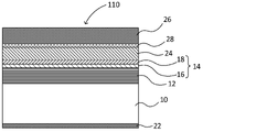
- FIG. 2 is a schematic cross-sectional view showing an example of the reflective mask blank 110 of this embodiment.
- a reflective mask blank 110 shown in FIG. 2 has an absorber film 24 for absorbing EUV light on the protective film 14 of the substrate 100 with a multilayer reflective film. Note that the reflective mask blank 110 can further have other thin films such as a resist film 26 on the absorber film 24 .
- FIG. 3 is a schematic cross-sectional view showing another example of the reflective mask blank 110 of this embodiment.
- the reflective mask blank 110 may have an etch mask film 28 between the absorber film 24 and the resist film 26 .
- the absorber film 24 of the reflective mask blank 110 of this embodiment is formed on the protective film 14 .
- the basic function of absorber film 24 is to absorb EUV light.
- the absorber film 24 may be an absorber film 24 intended to absorb EUV light, or an absorber film 24 having a phase shift function in consideration of the phase difference of EUV light.
- the absorber film 24 having a phase shift function absorbs EUV light and reflects part of the EUV light to shift the phase. That is, in the reflective mask 200 patterned with the absorber film 24 having a phase shift function, the portion where the absorber film 24 is formed absorbs the EUV light and attenuates the light, and does not adversely affect the pattern transfer. Reflect some EUV light at the level.
- the EUV light is reflected by the multilayer reflective film 12 via the protective film 14 . Therefore, a desired phase difference is generated between the reflected light from the absorber film 24 having a phase shift function and the reflected light from the field portion.
- the absorber film 24 having a phase shift function is preferably formed so that the phase difference between the reflected light from the absorber film 24 and the reflected light from the multilayer reflective film 12 is 170 degrees to 190 degrees.
- the image contrast of the projected optical image is improved by the interference of the light beams with the phase difference of about 180 degrees reversed at the pattern edge portion. As the image contrast is improved, the resolution is increased, and various latitudes related to exposure such as exposure amount latitude and focus latitude can be increased.
- the absorber film 24 may be a single-layer film, or may be a multilayer film composed of a plurality of films (for example, a lower-layer absorber film and an upper-layer absorber film).
- a single-layer film the number of steps in manufacturing mask blanks can be reduced, improving production efficiency.
- the optical constant and film thickness thereof can be appropriately set so that the upper absorber film serves as an anti-reflection film during mask pattern defect inspection using light. This improves the inspection sensitivity when inspecting mask pattern defects using light.
- a film added with oxygen (O), nitrogen (N), etc. which improves oxidation resistance, is used as the upper absorber film, the stability over time is improved.
- the absorber film 24 By making the absorber film 24 a multilayer film in this way, it is possible to add various functions to the absorber film 24 .
- the absorber film 24 has a phase shift function, it is possible to widen the range of adjustment on the optical surface by making it a multilayer film, making it easier to obtain a desired reflectance.
- the material of the absorber film 24 has a function of absorbing EUV light and can be processed by etching (preferably by dry etching with chlorine (Cl)-based gas and/or fluorine (F)-based gas). and is not particularly limited as long as the material has a high etching selectivity with respect to the protective film 14 .
- the absorber film 24 can be formed by magnetron sputtering such as DC sputtering and RF sputtering.
- the absorber film 24 made of a tantalum compound or the like can be formed by a reactive sputtering method using a target containing tantalum and boron and using argon gas to which oxygen or nitrogen is added.
- the tantalum compound for forming the absorber film 24 contains an alloy of Ta and the above metals.
- the crystalline state of the absorber film 24 is preferably amorphous or microcrystalline in terms of smoothness and flatness. If the surface of the absorber film 24 is not smooth or flat, the edge roughness of the absorber pattern 24a increases, and the dimensional accuracy of the pattern may deteriorate.
- the surface roughness of the absorber film 24 is preferably 0.5 nm or less, more preferably 0.4 nm or less, still more preferably 0.3 nm or less in terms of root mean square roughness (Rms).
- Examples of the tantalum compound for forming the absorber film 24 include a compound containing Ta and B, a compound containing Ta and N, a compound containing Ta, O and N, a compound containing Ta and B, and further O A compound containing at least one of and N, a compound containing Ta and Si, a compound containing Ta, Si and N, a compound containing Ta and Ge, and a compound containing Ta, Ge and N, and the like. be able to.
- Ta is a material that has a large absorption coefficient of EUV light and can be easily dry-etched with a chlorine-based gas or a fluorine-based gas. Therefore, it can be said that Ta is a material of the absorber film 24 with excellent workability. Furthermore, by adding B, Si and/or Ge to Ta, an amorphous material can be easily obtained. As a result, the smoothness of the absorber film 24 can be improved. Further, if N and/or O are added to Ta, the resistance to oxidation of the absorber film 24 is improved, so the stability over time can be improved.
- An etching mask film 28 may be formed on the absorber film 24 .
- FIG. The etching selectivity of the absorber film 24 to the etching mask film 28 is preferably 1.5 or more, more preferably 3 or more.
- the reflective mask blank 110 of this embodiment preferably has an etching mask film 28 containing chromium (Cr) on the absorber film 24 .
- Cr chromium
- chromium compounds include materials containing Cr and at least one element selected from N, O, C and H.
- the etching mask film 28 more preferably contains CrN, CrO, CrC, CrON, CrOC, CrCN, or CrOCN, and is a CrO-based film (CrO film, CrON film, CrOC film, or CrOCN film) containing chromium and oxygen. is more preferred.
- silicon or a silicon compound as the material for the etching mask film 28 .
- silicon compounds include materials containing Si and at least one element selected from N, O, C and H, metal silicon containing metals in silicon and silicon compounds (metal silicides), and metal silicon compounds (metal silicide compound) and the like.
- metal silicon compounds include materials containing metal, Si, and at least one element selected from N, O, C and H.
- the film thickness of the etching mask film 28 is preferably 3 nm or more in order to accurately form a pattern on the absorber film 24 . Moreover, the film thickness of the etching mask film 28 is preferably 15 nm or less in order to reduce the film thickness of the resist film 26 .
- a back surface conductive film 22 for electrostatic chuck may be formed on the back surface of the substrate 100 (the surface opposite to the side on which the multilayer reflective film 12 is formed).
- the sheet resistance required for the back surface conductive film 22 for electrostatic chucks is usually 100 ⁇ /square ( ⁇ /square) or less.
- the back conductive film 22 can be formed, for example, by magnetron sputtering or ion beam sputtering using a metal such as chromium or tantalum, or an alloy target thereof.
- the material of the back conductive film 22 is preferably a material containing chromium (Cr) or tantalum (Ta).
- the material of the back conductive film 22 is preferably a Cr compound containing Cr and at least one selected from boron, nitrogen, oxygen, and carbon.
- Cr compounds include CrN, CrON, CrCN, CrCON, CrBN, CrBON, CrBCN and CrBOCN.
- the material of the back conductive film 22 is preferably Ta (tantalum), an alloy containing Ta, or a Ta compound containing at least one of boron, nitrogen, oxygen, and carbon in any of these.
- Ta compounds include TaB, TaN, TaO, TaON, TaCON, TaBN, TaBO, TaBON, TaBCON, TaHf, TaHfO, TaHfN, TaHfON, TaHfCON, TaSi, TaSiO, TaSiN, TaSiON, and TaSiCON. can.
- the film thickness of the back-surface conductive film 22 is not particularly limited as long as it functions as a film for an electrostatic chuck, but is, for example, 10 nm to 200 nm.
- the reflective mask blank 110 of this embodiment can be used to manufacture the reflective mask 200 of this embodiment.
- An example of a method for manufacturing a reflective mask will be described below.
- FIG. 4A to 4E are schematic diagrams showing an example of a method for manufacturing the reflective mask 200.
- FIG. 4A to 4E are schematic diagrams showing an example of a method for manufacturing the reflective mask 200.
- a substrate 10 As shown in FIGS. 4A-E, first, a substrate 10, a multilayer reflective film 12 formed on the substrate 10, and a protective film 14 formed on the multilayer reflective film 12 (a Si material layer 16 and a protective layer 16). 18) and an absorber film 24 formed over the protective film 14 (FIG. 4A).
- a resist film 26 is formed on the absorber film 24 (FIG. 4B).
- a pattern is drawn on the resist film 26 by an electron beam drawing apparatus, and a resist pattern 26a is formed by developing and rinsing (FIG. 4C).
- the absorber film 24 is dry-etched. As a result, the portion of the absorber film 24 not covered with the resist pattern 26a is etched to form an absorber pattern 24a (FIG. 4D).
- etching gas for the absorber film 24 for example, a fluorine-based gas and/or a chlorine-based gas can be used.
- Fluorinated gases include CF4 , CHF3 , C2F6 , C3F6 , C4F6 , C4F8 , CH2F2 , CH3F , C3F8 , SF6 , and F2 . etc. can be used.
- Cl 2 , SiCl 4 , CHCl 3 , CCl 4 , BCl 3 and the like can be used as the chlorine-based gas.
- a mixed gas containing a fluorine-based gas and/or a chlorine-based gas and O 2 in a predetermined ratio can be used.
- These etching gases can optionally further contain inert gases such as He and/or Ar.
- the resist pattern 26a is removed with a resist remover. After removing the resist pattern 26a, the reflective mask 200 of this embodiment is obtained through a wet cleaning process using an acidic or alkaline aqueous solution (FIG. 4E).
- a pattern (etching mask pattern) is formed on the etching mask film 28 using the resist pattern 26a as a mask. After that, a process of forming a pattern on the absorber film 24 using the etching mask pattern as a mask is added.
- the reflective mask 200 thus obtained has a structure in which the multilayer reflective film 12, the protective film 14 (the Si material layer 16 and the protective layer 18), and the absorber pattern 24a are laminated on the substrate 10. is doing.
- a region 30 where the multilayer reflective film 12 (including the protective film 14) is exposed has the function of reflecting EUV light.
- a region 32 where the multilayer reflective film 12 (including the protective film 14) is covered with the absorber pattern 24a has the function of absorbing EUV light.
- the thickness of the absorber pattern 24a can be made thinner than before so that the reflectance becomes, for example, 2.5% or less. can be transferred to
- a transfer pattern can be formed on a semiconductor substrate by lithography using the reflective mask 200 of this embodiment. This transfer pattern has a shape obtained by transferring the pattern of the reflective mask 200 .
- a semiconductor device can be manufactured by forming a transfer pattern on a semiconductor substrate using the reflective mask 200 .
- FIG. 5 shows the pattern transfer device 50.
- the pattern transfer device 50 includes a laser plasma X-ray source 52, a reflective mask 200, a reduction optical system 54, and the like.
- An X-ray reflection mirror is used as the reduction optical system 54 .
- the pattern reflected by the reflective mask 200 is normally reduced to about 1/4 by the reduction optical system 54 .
- a wavelength band of 13 to 14 nm is used as the exposure wavelength, and the optical path is preset in a vacuum.
- the EUV light generated by the laser plasma X-ray source 52 is made incident on the reflective mask 200 .
- the light reflected by the reflective mask 200 is transferred onto the resist-coated semiconductor substrate 56 via the reduction optical system 54 .
- the light reflected by the reflective mask 200 enters the reduction optical system 54 .
- the light incident on the reduction optical system 54 forms a transfer pattern on the resist layer on the resist-coated semiconductor substrate 56 .
- a resist pattern can be formed on the resist-coated semiconductor substrate 56 by developing the exposed resist layer. By etching the semiconductor substrate 56 using the resist pattern as a mask, for example, a predetermined wiring pattern can be formed on the semiconductor substrate.
- a semiconductor device is manufactured through these processes and other necessary processes.
- a substrate 10 of 6025 size (approximately 152 mm ⁇ 152 mm ⁇ 6.35 mm) having polished first and second main surfaces was prepared.
- This substrate 10 is a substrate made of low thermal expansion glass (SiO 2 —TiO 2 based glass).
- the main surface of the substrate 10 was polished through a rough polishing process, a fine polishing process, a local polishing process, and a touch polishing process.
- a multilayer reflective film 12 was formed on the main surface (first main surface) of the substrate 10 .
- the multilayer reflective film 12 formed on the substrate 10 was a periodic multilayer reflective film 12 made of Mo and Si in order to make the multilayer reflective film 12 suitable for EUV light with a wavelength of 13.5 nm.
- the multilayer reflective film 12 was formed by alternately laminating a Mo film and a Si film on the substrate 10 by an ion beam sputtering method using a Mo target and a Si target and krypton (Kr) as a process gas.
- a Si film was formed with a thickness of 4.2 nm
- a Mo film was formed with a thickness of 2.8 nm. Taking this as one cycle, 40 cycles were laminated in the same manner to form the multilayer reflective film 12 .
- a Si material layer 16 was formed on the multilayer reflective film 12 .
- the Si material layer 16 was formed with a thickness of 3.5 nm by magnetron sputtering in an Ar gas atmosphere using a target made of a sintered SiC or sintered SiN.
- the SiC sintered body or SiN sintered body used as the target contains at least one selected from magnesium (Mg), aluminum (Al), yttrium (Y) and zirconium (Zr) as a sintering aid. Metal oxides were added.
- a SiN sintered body was used as a target to form the Si material layer. No sintering aid was added to this target.
- a SiC sintered body was used as a target to form the Si material layer. No sintering aid was added to this target.
- Si alone was used as a target to form a Si material layer.
- a RuNb film was formed as a protective layer 18 on the Si material layer 16 .
- the protective layer 18 was formed with a thickness of 3.5 nm by magnetron sputtering in an Ar gas atmosphere using a RuNb target.
- the reflectance to EUV light of the substrates 100 with multilayer reflective films of Examples, Reference Examples, and Comparative Examples was measured.
- the multilayer reflective film-attached substrate 100 was heated at 200° C. for 10 minutes in an air atmosphere. After heating the substrate 100 with the multilayer reflective film, the reflectance of the substrate 100 with the multilayer reflective film to EUV light was measured. By subtracting the reflectance (%) of the substrate 100 with the multilayer reflective film before heating from the reflectance (%) of the substrate 100 with the multilayer reflective film after heating, the change in the reflectance of the substrate 100 with the multilayer reflective film was evaluated. .
- the cross section of the protective film 14 was observed with an electron microscope to determine whether or not a SiO 2 layer was formed in the protective film 14 . confirmed.
- Table 1 below shows the results of confirming whether or not there was a change in the reflectance of the substrate 100 with a multilayer reflective film and whether or not a SiO 2 layer was formed in the protective film 14 .
- Table 1 below shows the film composition and film thickness of the Si material layer 16 in Examples, Reference Examples, and Comparative Examples after heating the substrate 100 with a multilayer reflective film.
- the film composition and metal oxides of the Si material layer 16 were measured by X-ray photoelectron spectroscopy (XPS) and dynamic SIMS (secondary ion mass spectrometry).
- the reflectance of the substrate 100 with the multilayer reflective film with respect to EUV light changed significantly before and after heating at 200°C.
- Si diffused from the Si material layer 16 to the protective layer 18 , so that metal silicide (RuSi) was formed in the protective layer 18 .
Landscapes
- Physics & Mathematics (AREA)
- General Physics & Mathematics (AREA)
- Chemical & Material Sciences (AREA)
- Chemical Kinetics & Catalysis (AREA)
- Engineering & Computer Science (AREA)
- Materials Engineering (AREA)
- Mechanical Engineering (AREA)
- Metallurgy (AREA)
- Organic Chemistry (AREA)
- Preparing Plates And Mask In Photomechanical Process (AREA)
- Exposure Of Semiconductors, Excluding Electron Or Ion Beam Exposure (AREA)
- Laminated Bodies (AREA)
Abstract
Description
前記保護膜は、前記多層反射膜と接する側に、ケイ素(Si)及び窒素(N)を含むSiN材料層又はケイ素(Si)及び炭素(C)を含むSiC材料層を含み、
前記SiN材料層又はSiC材料層は、マグネシウム(Mg)、アルミニウム(Al)、チタン(Ti)、イットリウム(Y)及びジルコニウム(Zr)から選択される少なくとも1つの金属の酸化物を含むことを特徴とする多層反射膜付き基板。 (Constitution 1) A substrate with a multilayer reflective film comprising a substrate, a multilayer reflective film provided on the substrate, and a protective film provided on the multilayer reflective film,
The protective film includes a SiN material layer containing silicon (Si) and nitrogen (N) or a SiC material layer containing silicon (Si) and carbon (C) on the side in contact with the multilayer reflective film,
The SiN material layer or the SiC material layer contains at least one metal oxide selected from magnesium (Mg), aluminum (Al), titanium (Ti), yttrium (Y) and zirconium (Zr). A substrate with a multilayer reflective film.
基板10は、EUV光による露光時の熱による転写パターンの歪みを防止するため、0±5ppb/℃の範囲内の低熱膨張係数を有するものが好ましく用いられる。この範囲の低熱膨張係数を有する素材としては、例えば、SiO2-TiO2系ガラス、多成分系ガラスセラミックス等を用いることができる。 <Substrate>
The
多層反射膜12は、屈折率の異なる元素を主成分とする複数の層が周期的に積層された構成を有している。一般的に、多層反射膜12は、高屈折率材料である軽元素又はその化合物の薄膜(高屈折率層)と、低屈折率材料である重元素又はその化合物の薄膜(低屈折率層)とが交互に40~60周期程度積層された多層膜からなる。 <Multilayer reflective film>
The multilayer
後述する反射型マスク200の製造工程におけるドライエッチング及び洗浄から多層反射膜12を保護するために、多層反射膜12の上に、又は多層反射膜12の表面に接するように保護膜14を形成することができる。また、保護膜14は、電子線(EB)を用いた転写パターン(吸収体パターン)の黒欠陥修正の際に、多層反射膜12を保護する機能も有している。多層反射膜12の上に保護膜14が形成されることにより、反射型マスク200を製造する際の多層反射膜12の表面へのダメージを抑制することができる。その結果、多層反射膜12のEUV光に対する反射率特性が良好となる。 <Protective film>
A
SiO2>TiO2>ZrO2>Al2O3>MgO>Y2O3 As described above, the SiN material layer or SiC material layer constituting the
SiO2 > TiO2 > ZrO2 > Al2O3 > MgO > Y2O3
本実施形態の反射型マスクブランク110の吸収体膜24は、保護膜14の上に形成される。吸収体膜24の基本的な機能は、EUV光を吸収することである。吸収体膜24は、EUV光の吸収を目的とした吸収体膜24であってもよいし、EUV光の位相差も考慮した位相シフト機能を有する吸収体膜24であっても良い。位相シフト機能を有する吸収体膜24とは、EUV光を吸収するとともに、EUV光の一部を反射させて位相をシフトさせるものである。すなわち、位相シフト機能を有する吸収体膜24がパターニングされた反射型マスク200において、吸収体膜24が形成されている部分では、EUV光を吸収して減光しつつ、パターン転写に悪影響がないレベルで一部のEUV光を反射させる。また、吸収体膜24が形成されていない領域(フィールド部)では、EUV光は、保護膜14を介して多層反射膜12で反射される。そのため、位相シフト機能を有する吸収体膜24からの反射光と、フィールド部からの反射光との間に所望の位相差が生ずる。位相シフト機能を有する吸収体膜24は、吸収体膜24からの反射光と、多層反射膜12からの反射光との位相差が170度から190度となるように形成されることが好ましい。180度近傍の反転した位相差の光同士がパターンエッジ部で干渉し合うことにより、投影光学像の像コントラストが向上する。その像コントラストの向上に伴って解像度が上がり、露光量裕度、及び焦点裕度等の露光に関する各種裕度を大きくすることができる。 <Absorber film>
The
吸収体膜24の上には、エッチングマスク膜28を形成してもよい。エッチングマスク膜28の材料としては、エッチングマスク膜28に対する吸収体膜24のエッチング選択比が高い材料を用いることが好ましい。エッチングマスク膜28に対する吸収体膜24のエッチング選択比は、1.5以上が好ましく、3以上が更に好ましい。 <Etching mask film>
An
基板100の裏面(多層反射膜12が形成された側と反対側の面)の上に、静電チャック用の裏面導電膜22を形成してもよい。静電チャック用として、裏面導電膜22に求められるシート抵抗は、通常100Ω/□(Ω/square)以下である。裏面導電膜22は、例えば、クロム又はタンタル等の金属、又はそれらの合金のターゲットを使用したマグネトロンスパッタリング法又はイオンビームスパッタリング法によって形成することができる。裏面導電膜22の材料は、クロム(Cr)又はタンタル(Ta)を含む材料であることが好ましい。例えば、裏面導電膜22の材料は、Crに、ホウ素、窒素、酸素、及び炭素から選択される少なくとも一つを含有したCr化合物であることが好ましい。Cr化合物としては、例えば、CrN、CrON、CrCN、CrCON、CrBN、CrBON、CrBCN及びCrBOCNなどを挙げることができる。また、裏面導電膜22の材料は、Ta(タンタル)、Taを含有する合金、又はこれらのいずれかにホウ素、窒素、酸素、及び炭素の少なくとも一つを含有したTa化合物であることが好ましい。Ta化合物としては、例えば、TaB、TaN、TaO、TaON、TaCON、TaBN、TaBO、TaBON、TaBCON、TaHf、TaHfO、TaHfN、TaHfON、TaHfCON、TaSi、TaSiO、TaSiN、TaSiON、及びTaSiCONなどを挙げることができる。 <Back surface conductive film>
A back surface
本実施形態の反射型マスクブランク110を使用して、本実施形態の反射型マスク200を製造することができる。以下、反射型マスクの製造方法の例について説明する。 <Reflective mask>
The reflective mask blank 110 of this embodiment can be used to manufacture the
本実施形態の反射型マスク200を使用したリソグラフィーにより、半導体基板上に転写パターンを形成することができる。この転写パターンは、反射型マスク200のパターンが転写された形状を有している。半導体基板上に反射型マスク200によって転写パターンを形成することによって、半導体装置を製造することができる。 <Method for manufacturing a semiconductor device>
A transfer pattern can be formed on a semiconductor substrate by lithography using the
まず、第1主表面及び第2主表面が研磨された6025サイズ(約152mm×152mm×6.35mm)の基板10を準備した。この基板10は、低熱膨張ガラス(SiO2-TiO2系ガラス)からなる基板である。基板10の主表面は、粗研磨加工工程、精密研磨加工工程、局所加工工程、及びタッチ研磨加工工程によって研磨した。 (Preparation of
First, a
上記で作製した実施例、参考例及び比較例の多層反射膜付き基板100を用いて、多層反射膜付き基板100を加熱した後の反射率の変化の有無、及び、保護膜14中のSiO2層の形成の有無を確認した。 (Evaluation of
Using the multilayer reflective film-attached

12 多層反射膜
14 保護膜
16 Si材料層
18 保護層
22 裏面導電膜
24a 吸収体パターン
24 吸収体膜
26a レジストパターン
26 レジスト膜
28 エッチングマスク膜
50 パターン転写装置
100 多層反射膜付き基板
110 反射型マスクブランク
200 反射型マスク 10
Claims (6)
- 基板と、該基板の上に設けられた多層反射膜と、該多層反射膜の上に設けられた保護膜とを有する多層反射膜付き基板であって、
前記保護膜は、前記多層反射膜と接する側に、ケイ素(Si)及び窒素(N)を含むSiN材料層又はケイ素(Si)及び炭素(C)を含むSiC材料層を含み、
前記SiN材料層又はSiC材料層は、マグネシウム(Mg)、アルミニウム(Al)、チタン(Ti)、イットリウム(Y)及びジルコニウム(Zr)から選択される少なくとも1つの金属の酸化物を含むことを特徴とする多層反射膜付き基板。 A substrate with a multilayer reflective film comprising a substrate, a multilayer reflective film provided on the substrate, and a protective film provided on the multilayer reflective film,
The protective film includes a SiN material layer containing silicon (Si) and nitrogen (N) or a SiC material layer containing silicon (Si) and carbon (C) on the side in contact with the multilayer reflective film,
The SiN material layer or the SiC material layer contains at least one metal oxide selected from magnesium (Mg), aluminum (Al), titanium (Ti), yttrium (Y) and zirconium (Zr). A substrate with a multilayer reflective film. - 前記金属は、Y及びZrから選択される少なくとも1つであることを特徴とする請求項1記載の多層反射膜付き基板。 The substrate with a multilayer reflective film according to claim 1, wherein the metal is at least one selected from Y and Zr.
- 前記保護膜は、前記SiN材料層又はSiC材料層の上にRu系材料層を含むことを特徴とする請求項1又は2に記載の多層反射膜付き基板。 The substrate with a multilayer reflective film according to claim 1 or 2, wherein the protective film includes a Ru-based material layer on the SiN material layer or the SiC material layer.
- 請求項1乃至3の何れか1項に記載の多層反射膜付き基板の前記保護膜の上に、吸収体膜を備えることを特徴とする反射型マスクブランク。 A reflective mask blank, comprising an absorber film on the protective film of the substrate with a multilayer reflective film according to any one of claims 1 to 3.
- 請求項4に記載の反射型マスクブランクの前記吸収体膜をパターニングした吸収体パターンを備えることを特徴とする反射型マスク。 A reflective mask comprising an absorber pattern obtained by patterning the absorber film of the reflective mask blank according to claim 4.
- 請求項5に記載の反射型マスクを用いて、露光装置を使用したリソグラフィプロセスを行い、被転写体に転写パターンを形成する工程を有することを特徴とする半導体装置の製造方法。 A method of manufacturing a semiconductor device, comprising a step of performing a lithography process using an exposure apparatus using the reflective mask according to claim 5 to form a transfer pattern on a transfer target.
Priority Applications (3)
| Application Number | Priority Date | Filing Date | Title |
|---|---|---|---|
| KR1020237026284A KR20230148328A (en) | 2021-03-02 | 2022-02-22 | Manufacturing method of multilayer reflective film-attached substrate, reflective mask blank, reflective mask, and semiconductor device |
| JP2023503740A JPWO2022186004A1 (en) | 2021-03-02 | 2022-02-22 | |
| US18/277,648 US20240231214A9 (en) | 2021-03-02 | 2022-02-22 | Substrate with multilayer reflective film, reflective mask blank, reflective mask, and method for manufacturing semiconductor device |
Applications Claiming Priority (2)
| Application Number | Priority Date | Filing Date | Title |
|---|---|---|---|
| JP2021-032542 | 2021-03-02 | ||
| JP2021032542 | 2021-03-02 |
Publications (1)
| Publication Number | Publication Date |
|---|---|
| WO2022186004A1 true WO2022186004A1 (en) | 2022-09-09 |
Family
ID=83154389
Family Applications (1)
| Application Number | Title | Priority Date | Filing Date |
|---|---|---|---|
| PCT/JP2022/007287 WO2022186004A1 (en) | 2021-03-02 | 2022-02-22 | Substrate with multilayer reflective film, reflective mask blank, reflective mask, and method for manufacturing semiconductor device |
Country Status (5)
| Country | Link |
|---|---|
| US (1) | US20240231214A9 (en) |
| JP (1) | JPWO2022186004A1 (en) |
| KR (1) | KR20230148328A (en) |
| TW (1) | TW202248742A (en) |
| WO (1) | WO2022186004A1 (en) |
Citations (5)
| Publication number | Priority date | Publication date | Assignee | Title |
|---|---|---|---|---|
| JP2004342867A (en) * | 2003-05-16 | 2004-12-02 | Hoya Corp | Reflective mask blank and reflective mask |
| JP2007294840A (en) * | 2006-03-30 | 2007-11-08 | Toppan Printing Co Ltd | Reflective photomask blank and its manufacturing method, reflective photomask, and method for manufacturing semiconductor device |
| JP2008277398A (en) * | 2007-04-26 | 2008-11-13 | Toppan Printing Co Ltd | Extreme ultraviolet exposure mask, and mask blank |
| JP2008288361A (en) * | 2007-05-17 | 2008-11-27 | Toppan Printing Co Ltd | Reflection type photo mask blank, manufacturing method thereof, reflection type photo mask blank, and manufacturing method of semiconductor device |
| JP2014042056A (en) * | 2006-09-15 | 2014-03-06 | Applied Materials Inc | Method of etching extreme ultraviolet light (euv) photomasks |
Family Cites Families (2)
| Publication number | Priority date | Publication date | Assignee | Title |
|---|---|---|---|---|
| JP6377361B2 (en) | 2013-02-11 | 2018-08-22 | Hoya株式会社 | SUBSTRATE WITH MULTILAYER REFLECTIVE FILM AND METHOD FOR MANUFACTURING THE SAME, METHOD FOR PRODUCING REFLECTIVE MASK BLANK, METHOD FOR PRODUCING REFLECTIVE MASK, AND METHOD FOR MANUFACTURING SEMICONDUCTOR DEVICE |
| US9740091B2 (en) | 2013-07-22 | 2017-08-22 | Hoya Corporation | Substrate with multilayer reflective film, reflective mask blank for EUV lithography, reflective mask for EUV lithography, and method of manufacturing the same, and method of manufacturing a semiconductor device |
-
2022
- 2022-02-22 US US18/277,648 patent/US20240231214A9/en active Pending
- 2022-02-22 JP JP2023503740A patent/JPWO2022186004A1/ja active Pending
- 2022-02-22 KR KR1020237026284A patent/KR20230148328A/en unknown
- 2022-02-22 WO PCT/JP2022/007287 patent/WO2022186004A1/en active Application Filing
- 2022-03-02 TW TW111107514A patent/TW202248742A/en unknown
Patent Citations (5)
| Publication number | Priority date | Publication date | Assignee | Title |
|---|---|---|---|---|
| JP2004342867A (en) * | 2003-05-16 | 2004-12-02 | Hoya Corp | Reflective mask blank and reflective mask |
| JP2007294840A (en) * | 2006-03-30 | 2007-11-08 | Toppan Printing Co Ltd | Reflective photomask blank and its manufacturing method, reflective photomask, and method for manufacturing semiconductor device |
| JP2014042056A (en) * | 2006-09-15 | 2014-03-06 | Applied Materials Inc | Method of etching extreme ultraviolet light (euv) photomasks |
| JP2008277398A (en) * | 2007-04-26 | 2008-11-13 | Toppan Printing Co Ltd | Extreme ultraviolet exposure mask, and mask blank |
| JP2008288361A (en) * | 2007-05-17 | 2008-11-27 | Toppan Printing Co Ltd | Reflection type photo mask blank, manufacturing method thereof, reflection type photo mask blank, and manufacturing method of semiconductor device |
Also Published As
| Publication number | Publication date |
|---|---|
| JPWO2022186004A1 (en) | 2022-09-09 |
| TW202248742A (en) | 2022-12-16 |
| US20240231214A9 (en) | 2024-07-11 |
| KR20230148328A (en) | 2023-10-24 |
| US20240134265A1 (en) | 2024-04-25 |
Similar Documents
| Publication | Publication Date | Title |
|---|---|---|
| JP7502510B2 (en) | Reflective mask blank, reflective mask, and method for manufacturing semiconductor device | |
| TWI811369B (en) | Reflective photomask base, reflective photomask, method for manufacturing reflective photomask and semiconductor device | |
| JP7193344B2 (en) | Reflective mask blank, method for manufacturing reflective mask, and method for manufacturing semiconductor device | |
| JP7401356B2 (en) | Substrate with multilayer reflective film, reflective mask blank, reflective mask, and semiconductor device manufacturing method | |
| JP7263908B2 (en) | Reflective mask blank, reflective mask, and method for manufacturing reflective mask blank | |
| JP7475154B2 (en) | Reflective mask blank, reflective mask, substrate with conductive film, and method for manufacturing semiconductor device | |
| JP7268211B2 (en) | Reflective mask blank, reflective mask, manufacturing method thereof, and manufacturing method of semiconductor device | |
| JP2021056502A (en) | Substrate with multi-layered reflecting film, reflective mask blank, reflective mask and method for manufacturing the same, and method for manufacturing semiconductor device | |
| KR20230119120A (en) | Manufacturing method of reflective mask blank, reflective mask and semiconductor device | |
| JP2024097036A (en) | Substrate with multilayer reflective film, reflective mask blank, reflective mask, and method for manufacturing semiconductor device | |
| JP2024075660A (en) | Substrate with multilayer reflective film, reflective mask blank, reflective mask, and method for manufacturing semiconductor device | |
| KR20220054280A (en) | A substrate with a multilayer reflective film, a reflective mask blank and a reflective mask, and a method for manufacturing a semiconductor device | |
| JP2022159362A (en) | Substrate with multilayer reflective film, reflective type mask blank and reflective type mask, and method for manufacturing semiconductor device | |
| WO2021200325A1 (en) | Multilayer reflective film-equipped substrate, reflective mask blank, reflective mask, and method for producing semiconductor device | |
| JP6223756B2 (en) | Multilayer reflective film-coated substrate, reflective mask blank for EUV lithography, reflective mask for EUV lithography, method for manufacturing the same, and method for manufacturing a semiconductor device | |
| JP2023171382A (en) | Substrate with electroconductive film, reflective mask blank, reflective mask, and method for producing semiconductor device | |
| WO2022210334A1 (en) | Reflective mask blank, reflective mask, method for manufacturing reflective mask, and method for manufacturing semiconductor device | |
| WO2022138434A1 (en) | Multilayer reflective film-equipped substrate, reflective mask blank, reflective mask, and method for producing semiconductor device | |
| WO2022186004A1 (en) | Substrate with multilayer reflective film, reflective mask blank, reflective mask, and method for manufacturing semiconductor device | |
| TW202219625A (en) | Multilayer reflective film-equipped substrate, reflective mask blank, reflective mask manufacturing method, and semiconductor device manufacturing method | |
| WO2023054145A1 (en) | Multilayer reflective film-equipped substrate, reflective mask blank, reflective mask, and method for manufacturing semiconductor device | |
| WO2024085026A1 (en) | Reflective mask blank, reflective mask, and manufacturing methods for reflective mask and semiconductor device | |
| WO2023074770A1 (en) | Multilayer reflective film-attached substrate, reflective mask blank, reflective mask, and method for producing semiconductor device | |
| WO2024005038A1 (en) | Substrate with multilayer reflective film, reflective mask blank, reflective mask, and method for producing semiconductor device | |
| WO2024071026A1 (en) | Substrate with conductive film, reflective mask blank, reflective mask, and semiconductor device production method |
Legal Events
| Date | Code | Title | Description |
|---|---|---|---|
| 121 | Ep: the epo has been informed by wipo that ep was designated in this application |
Ref document number: 22763060 Country of ref document: EP Kind code of ref document: A1 |
|
| WWE | Wipo information: entry into national phase |
Ref document number: 2023503740 Country of ref document: JP |
|
| WWE | Wipo information: entry into national phase |
Ref document number: 18277648 Country of ref document: US |
|
| NENP | Non-entry into the national phase |
Ref country code: DE |
|
| 122 | Ep: pct application non-entry in european phase |
Ref document number: 22763060 Country of ref document: EP Kind code of ref document: A1 |