WO2024005038A1 - Substrate with multilayer reflective film, reflective mask blank, reflective mask, and method for producing semiconductor device - Google Patents
Substrate with multilayer reflective film, reflective mask blank, reflective mask, and method for producing semiconductor device Download PDFInfo
- Publication number
- WO2024005038A1 WO2024005038A1 PCT/JP2023/023882 JP2023023882W WO2024005038A1 WO 2024005038 A1 WO2024005038 A1 WO 2024005038A1 JP 2023023882 W JP2023023882 W JP 2023023882W WO 2024005038 A1 WO2024005038 A1 WO 2024005038A1
- Authority
- WO
- WIPO (PCT)
- Prior art keywords
- layer
- film
- content
- protective film
- multilayer reflective
- Prior art date
Links
- 239000000758 substrate Substances 0.000 title claims abstract description 173
- 239000004065 semiconductor Substances 0.000 title claims description 30
- 238000004519 manufacturing process Methods 0.000 title claims description 27
- 230000001681 protective effect Effects 0.000 claims abstract description 216
- 229910052751 metal Inorganic materials 0.000 claims abstract description 124
- 239000002184 metal Substances 0.000 claims abstract description 118
- 239000000654 additive Substances 0.000 claims abstract description 70
- 230000000996 additive effect Effects 0.000 claims abstract description 70
- 238000009826 distribution Methods 0.000 claims abstract description 60
- IJGRMHOSHXDMSA-UHFFFAOYSA-N Atomic nitrogen Chemical compound N#N IJGRMHOSHXDMSA-UHFFFAOYSA-N 0.000 claims description 134
- 239000006096 absorbing agent Substances 0.000 claims description 100
- 229910052760 oxygen Inorganic materials 0.000 claims description 69
- 229910052757 nitrogen Inorganic materials 0.000 claims description 66
- QVGXLLKOCUKJST-UHFFFAOYSA-N atomic oxygen Chemical compound [O] QVGXLLKOCUKJST-UHFFFAOYSA-N 0.000 claims description 65
- 239000001301 oxygen Substances 0.000 claims description 65
- 238000000034 method Methods 0.000 claims description 50
- 229910052710 silicon Inorganic materials 0.000 claims description 44
- 239000010703 silicon Substances 0.000 claims description 39
- XUIMIQQOPSSXEZ-UHFFFAOYSA-N Silicon Chemical compound [Si] XUIMIQQOPSSXEZ-UHFFFAOYSA-N 0.000 claims description 38
- 239000010948 rhodium Substances 0.000 claims description 26
- 238000012546 transfer Methods 0.000 claims description 20
- 230000008569 process Effects 0.000 claims description 15
- 229910052703 rhodium Inorganic materials 0.000 claims description 15
- 229910052707 ruthenium Inorganic materials 0.000 claims description 15
- 229910052750 molybdenum Inorganic materials 0.000 claims description 12
- 229910052758 niobium Inorganic materials 0.000 claims description 12
- 229910052718 tin Inorganic materials 0.000 claims description 12
- KJTLSVCANCCWHF-UHFFFAOYSA-N Ruthenium Chemical compound [Ru] KJTLSVCANCCWHF-UHFFFAOYSA-N 0.000 claims description 11
- 229910052719 titanium Inorganic materials 0.000 claims description 11
- 229910052735 hafnium Inorganic materials 0.000 claims description 10
- 229910052741 iridium Inorganic materials 0.000 claims description 10
- 229910052727 yttrium Inorganic materials 0.000 claims description 10
- MHOVAHRLVXNVSD-UHFFFAOYSA-N rhodium atom Chemical compound [Rh] MHOVAHRLVXNVSD-UHFFFAOYSA-N 0.000 claims description 9
- 229910052720 vanadium Inorganic materials 0.000 claims description 9
- 229910052726 zirconium Inorganic materials 0.000 claims description 9
- GKOZUEZYRPOHIO-UHFFFAOYSA-N iridium atom Chemical compound [Ir] GKOZUEZYRPOHIO-UHFFFAOYSA-N 0.000 claims description 8
- 229910052782 aluminium Inorganic materials 0.000 claims description 7
- 229910052802 copper Inorganic materials 0.000 claims description 7
- 229910052748 manganese Inorganic materials 0.000 claims description 7
- 229910052709 silver Inorganic materials 0.000 claims description 7
- 229910052721 tungsten Inorganic materials 0.000 claims description 7
- 229910052738 indium Inorganic materials 0.000 claims description 6
- 229910052745 lead Inorganic materials 0.000 claims description 6
- 229910052716 thallium Inorganic materials 0.000 claims description 6
- 229910052725 zinc Inorganic materials 0.000 claims description 6
- 238000001459 lithography Methods 0.000 claims description 4
- 239000010408 film Substances 0.000 description 618
- 239000010410 layer Substances 0.000 description 545
- 239000010409 thin film Substances 0.000 description 88
- 238000005530 etching Methods 0.000 description 69
- 239000000463 material Substances 0.000 description 39
- 239000007789 gas Substances 0.000 description 36
- 239000011651 chromium Substances 0.000 description 24
- 230000007423 decrease Effects 0.000 description 24
- 230000007547 defect Effects 0.000 description 18
- 238000009792 diffusion process Methods 0.000 description 15
- 229910052799 carbon Inorganic materials 0.000 description 14
- 238000010438 heat treatment Methods 0.000 description 14
- 238000012889 quartic function Methods 0.000 description 14
- 230000015572 biosynthetic process Effects 0.000 description 13
- 229910052804 chromium Inorganic materials 0.000 description 13
- 239000000203 mixture Substances 0.000 description 13
- 230000003287 optical effect Effects 0.000 description 13
- 230000003647 oxidation Effects 0.000 description 12
- 238000007254 oxidation reaction Methods 0.000 description 12
- OKTJSMMVPCPJKN-UHFFFAOYSA-N Carbon Chemical compound [C] OKTJSMMVPCPJKN-UHFFFAOYSA-N 0.000 description 11
- 229910052739 hydrogen Inorganic materials 0.000 description 11
- 239000010955 niobium Substances 0.000 description 11
- BASFCYQUMIYNBI-UHFFFAOYSA-N platinum Chemical compound [Pt] BASFCYQUMIYNBI-UHFFFAOYSA-N 0.000 description 10
- 238000005546 reactive sputtering Methods 0.000 description 10
- 239000011135 tin Substances 0.000 description 10
- 239000010936 titanium Substances 0.000 description 10
- 229910052796 boron Inorganic materials 0.000 description 9
- 150000001875 compounds Chemical class 0.000 description 9
- 229910052715 tantalum Inorganic materials 0.000 description 9
- ZOXJGFHDIHLPTG-UHFFFAOYSA-N Boron Chemical compound [B] ZOXJGFHDIHLPTG-UHFFFAOYSA-N 0.000 description 8
- 229910045601 alloy Inorganic materials 0.000 description 8
- 239000000956 alloy Substances 0.000 description 8
- 239000000460 chlorine Substances 0.000 description 8
- 239000010949 copper Substances 0.000 description 8
- 238000001659 ion-beam spectroscopy Methods 0.000 description 8
- 238000001755 magnetron sputter deposition Methods 0.000 description 8
- UFHFLCQGNIYNRP-UHFFFAOYSA-N Hydrogen Chemical compound [H][H] UFHFLCQGNIYNRP-UHFFFAOYSA-N 0.000 description 7
- 238000010586 diagram Methods 0.000 description 7
- 238000002149 energy-dispersive X-ray emission spectroscopy Methods 0.000 description 7
- 238000001900 extreme ultraviolet lithography Methods 0.000 description 7
- 239000001257 hydrogen Substances 0.000 description 7
- 239000000243 solution Substances 0.000 description 7
- ATJFFYVFTNAWJD-UHFFFAOYSA-N Tin Chemical compound [Sn] ATJFFYVFTNAWJD-UHFFFAOYSA-N 0.000 description 6
- 229910052731 fluorine Inorganic materials 0.000 description 6
- 230000010363 phase shift Effects 0.000 description 6
- 230000002265 prevention Effects 0.000 description 6
- GUVRBAGPIYLISA-UHFFFAOYSA-N tantalum atom Chemical compound [Ta] GUVRBAGPIYLISA-UHFFFAOYSA-N 0.000 description 6
- ZAMOUSCENKQFHK-UHFFFAOYSA-N Chlorine atom Chemical compound [Cl] ZAMOUSCENKQFHK-UHFFFAOYSA-N 0.000 description 5
- VYZAMTAEIAYCRO-UHFFFAOYSA-N Chromium Chemical compound [Cr] VYZAMTAEIAYCRO-UHFFFAOYSA-N 0.000 description 5
- YCKRFDGAMUMZLT-UHFFFAOYSA-N Fluorine atom Chemical compound [F] YCKRFDGAMUMZLT-UHFFFAOYSA-N 0.000 description 5
- 229910052801 chlorine Inorganic materials 0.000 description 5
- 238000004140 cleaning Methods 0.000 description 5
- 229910001873 dinitrogen Inorganic materials 0.000 description 5
- 230000000694 effects Effects 0.000 description 5
- 239000011737 fluorine Substances 0.000 description 5
- 230000007774 longterm Effects 0.000 description 5
- 239000011572 manganese Substances 0.000 description 5
- 238000005259 measurement Methods 0.000 description 5
- 230000000737 periodic effect Effects 0.000 description 5
- XKRFYHLGVUSROY-UHFFFAOYSA-N Argon Chemical compound [Ar] XKRFYHLGVUSROY-UHFFFAOYSA-N 0.000 description 4
- ZOKXTWBITQBERF-UHFFFAOYSA-N Molybdenum Chemical compound [Mo] ZOKXTWBITQBERF-UHFFFAOYSA-N 0.000 description 4
- 238000010521 absorption reaction Methods 0.000 description 4
- 230000002411 adverse Effects 0.000 description 4
- 238000004458 analytical method Methods 0.000 description 4
- 230000008033 biological extinction Effects 0.000 description 4
- 230000005540 biological transmission Effects 0.000 description 4
- 239000000470 constituent Substances 0.000 description 4
- 239000011733 molybdenum Substances 0.000 description 4
- PXHVJJICTQNCMI-UHFFFAOYSA-N nickel Substances [Ni] PXHVJJICTQNCMI-UHFFFAOYSA-N 0.000 description 4
- KDLHZDBZIXYQEI-UHFFFAOYSA-N palladium Substances [Pd] KDLHZDBZIXYQEI-UHFFFAOYSA-N 0.000 description 4
- 238000000059 patterning Methods 0.000 description 4
- 229910052697 platinum Inorganic materials 0.000 description 4
- 238000007517 polishing process Methods 0.000 description 4
- 150000003377 silicon compounds Chemical class 0.000 description 4
- 229910004535 TaBN Inorganic materials 0.000 description 3
- 238000004833 X-ray photoelectron spectroscopy Methods 0.000 description 3
- 229910052786 argon Inorganic materials 0.000 description 3
- 230000008859 change Effects 0.000 description 3
- 238000012888 cubic function Methods 0.000 description 3
- 230000004069 differentiation Effects 0.000 description 3
- 239000011521 glass Substances 0.000 description 3
- 239000010931 gold Substances 0.000 description 3
- 238000007689 inspection Methods 0.000 description 3
- 238000010030 laminating Methods 0.000 description 3
- 238000005121 nitriding Methods 0.000 description 3
- 230000001590 oxidative effect Effects 0.000 description 3
- 239000012466 permeate Substances 0.000 description 3
- 229910021332 silicide Inorganic materials 0.000 description 3
- 229910052814 silicon oxide Inorganic materials 0.000 description 3
- 238000009751 slip forming Methods 0.000 description 3
- 238000004544 sputter deposition Methods 0.000 description 3
- 239000000126 substance Substances 0.000 description 3
- 230000003746 surface roughness Effects 0.000 description 3
- 150000003482 tantalum compounds Chemical class 0.000 description 3
- 239000011701 zinc Substances 0.000 description 3
- CURLTUGMZLYLDI-UHFFFAOYSA-N Carbon dioxide Chemical compound O=C=O CURLTUGMZLYLDI-UHFFFAOYSA-N 0.000 description 2
- HEDRZPFGACZZDS-UHFFFAOYSA-N Chloroform Chemical compound ClC(Cl)Cl HEDRZPFGACZZDS-UHFFFAOYSA-N 0.000 description 2
- 229910052581 Si3N4 Inorganic materials 0.000 description 2
- 229910004298 SiO 2 Inorganic materials 0.000 description 2
- VYPSYNLAJGMNEJ-UHFFFAOYSA-N Silicium dioxide Chemical compound O=[Si]=O VYPSYNLAJGMNEJ-UHFFFAOYSA-N 0.000 description 2
- 229910010413 TiO 2 Inorganic materials 0.000 description 2
- RTAQQCXQSZGOHL-UHFFFAOYSA-N Titanium Chemical compound [Ti] RTAQQCXQSZGOHL-UHFFFAOYSA-N 0.000 description 2
- 150000001845 chromium compounds Chemical class 0.000 description 2
- 238000001312 dry etching Methods 0.000 description 2
- 238000005516 engineering process Methods 0.000 description 2
- 229910052737 gold Inorganic materials 0.000 description 2
- 150000002431 hydrogen Chemical class 0.000 description 2
- 238000010884 ion-beam technique Methods 0.000 description 2
- 150000002500 ions Chemical class 0.000 description 2
- 238000012886 linear function Methods 0.000 description 2
- 239000011777 magnesium Substances 0.000 description 2
- 239000012528 membrane Substances 0.000 description 2
- 239000007769 metal material Substances 0.000 description 2
- -1 metal silicon compounds Chemical class 0.000 description 2
- 150000002739 metals Chemical class 0.000 description 2
- 229910052759 nickel Inorganic materials 0.000 description 2
- GUCVJGMIXFAOAE-UHFFFAOYSA-N niobium atom Chemical compound [Nb] GUCVJGMIXFAOAE-UHFFFAOYSA-N 0.000 description 2
- 150000004767 nitrides Chemical class 0.000 description 2
- 229910052763 palladium Inorganic materials 0.000 description 2
- 239000002245 particle Substances 0.000 description 2
- 230000009257 reactivity Effects 0.000 description 2
- VSZWPYCFIRKVQL-UHFFFAOYSA-N selanylidenegallium;selenium Chemical compound [Se].[Se]=[Ga].[Se]=[Ga] VSZWPYCFIRKVQL-UHFFFAOYSA-N 0.000 description 2
- FVBUAEGBCNSCDD-UHFFFAOYSA-N silicide(4-) Chemical compound [Si-4] FVBUAEGBCNSCDD-UHFFFAOYSA-N 0.000 description 2
- HQVNEWCFYHHQES-UHFFFAOYSA-N silicon nitride Chemical compound N12[Si]34N5[Si]62N3[Si]51N64 HQVNEWCFYHHQES-UHFFFAOYSA-N 0.000 description 2
- 239000002356 single layer Substances 0.000 description 2
- VZGDMQKNWNREIO-UHFFFAOYSA-N tetrachloromethane Chemical compound ClC(Cl)(Cl)Cl VZGDMQKNWNREIO-UHFFFAOYSA-N 0.000 description 2
- 238000007738 vacuum evaporation Methods 0.000 description 2
- 238000007740 vapor deposition Methods 0.000 description 2
- VWQVUPCCIRVNHF-UHFFFAOYSA-N yttrium atom Chemical compound [Y] VWQVUPCCIRVNHF-UHFFFAOYSA-N 0.000 description 2
- 229910015844 BCl3 Inorganic materials 0.000 description 1
- WKBOTKDWSSQWDR-UHFFFAOYSA-N Bromine atom Chemical compound [Br] WKBOTKDWSSQWDR-UHFFFAOYSA-N 0.000 description 1
- 101150013999 CRBN gene Proteins 0.000 description 1
- KZBUYRJDOAKODT-UHFFFAOYSA-N Chlorine Chemical compound ClCl KZBUYRJDOAKODT-UHFFFAOYSA-N 0.000 description 1
- RYGMFSIKBFXOCR-UHFFFAOYSA-N Copper Chemical compound [Cu] RYGMFSIKBFXOCR-UHFFFAOYSA-N 0.000 description 1
- MYMOFIZGZYHOMD-UHFFFAOYSA-N Dioxygen Chemical compound O=O MYMOFIZGZYHOMD-UHFFFAOYSA-N 0.000 description 1
- XEEYBQQBJWHFJM-UHFFFAOYSA-N Iron Chemical compound [Fe] XEEYBQQBJWHFJM-UHFFFAOYSA-N 0.000 description 1
- FYYHWMGAXLPEAU-UHFFFAOYSA-N Magnesium Chemical compound [Mg] FYYHWMGAXLPEAU-UHFFFAOYSA-N 0.000 description 1
- PWHULOQIROXLJO-UHFFFAOYSA-N Manganese Chemical compound [Mn] PWHULOQIROXLJO-UHFFFAOYSA-N 0.000 description 1
- 229910003910 SiCl4 Inorganic materials 0.000 description 1
- BQCADISMDOOEFD-UHFFFAOYSA-N Silver Chemical compound [Ag] BQCADISMDOOEFD-UHFFFAOYSA-N 0.000 description 1
- 229910004166 TaN Inorganic materials 0.000 description 1
- 229910004158 TaO Inorganic materials 0.000 description 1
- 229910003071 TaON Inorganic materials 0.000 description 1
- 230000002378 acidificating effect Effects 0.000 description 1
- XAGFODPZIPBFFR-UHFFFAOYSA-N aluminium Chemical compound [Al] XAGFODPZIPBFFR-UHFFFAOYSA-N 0.000 description 1
- 238000000137 annealing Methods 0.000 description 1
- 239000007864 aqueous solution Substances 0.000 description 1
- GDTBXPJZTBHREO-UHFFFAOYSA-N bromine Substances BrBr GDTBXPJZTBHREO-UHFFFAOYSA-N 0.000 description 1
- 229910052794 bromium Inorganic materials 0.000 description 1
- 229910002092 carbon dioxide Inorganic materials 0.000 description 1
- 239000001569 carbon dioxide Substances 0.000 description 1
- 239000011248 coating agent Substances 0.000 description 1
- 238000000576 coating method Methods 0.000 description 1
- 229910017052 cobalt Inorganic materials 0.000 description 1
- 239000010941 cobalt Substances 0.000 description 1
- GUTLYIVDDKVIGB-UHFFFAOYSA-N cobalt atom Chemical compound [Co] GUTLYIVDDKVIGB-UHFFFAOYSA-N 0.000 description 1
- 238000011109 contamination Methods 0.000 description 1
- 230000003247 decreasing effect Effects 0.000 description 1
- 238000000151 deposition Methods 0.000 description 1
- 230000008021 deposition Effects 0.000 description 1
- 230000006866 deterioration Effects 0.000 description 1
- 238000011161 development Methods 0.000 description 1
- 229910001882 dioxygen Inorganic materials 0.000 description 1
- 239000002019 doping agent Substances 0.000 description 1
- 238000010894 electron beam technology Methods 0.000 description 1
- 229910052732 germanium Inorganic materials 0.000 description 1
- GNPVGFCGXDBREM-UHFFFAOYSA-N germanium atom Chemical compound [Ge] GNPVGFCGXDBREM-UHFFFAOYSA-N 0.000 description 1
- 239000002241 glass-ceramic Substances 0.000 description 1
- PCHJSUWPFVWCPO-UHFFFAOYSA-N gold Chemical compound [Au] PCHJSUWPFVWCPO-UHFFFAOYSA-N 0.000 description 1
- VBJZVLUMGGDVMO-UHFFFAOYSA-N hafnium atom Chemical compound [Hf] VBJZVLUMGGDVMO-UHFFFAOYSA-N 0.000 description 1
- 239000011261 inert gas Substances 0.000 description 1
- 229910052743 krypton Inorganic materials 0.000 description 1
- DNNSSWSSYDEUBZ-UHFFFAOYSA-N krypton atom Chemical compound [Kr] DNNSSWSSYDEUBZ-UHFFFAOYSA-N 0.000 description 1
- 229910052746 lanthanum Inorganic materials 0.000 description 1
- FZLIPJUXYLNCLC-UHFFFAOYSA-N lanthanum atom Chemical compound [La] FZLIPJUXYLNCLC-UHFFFAOYSA-N 0.000 description 1
- 229910052749 magnesium Inorganic materials 0.000 description 1
- 101150016677 ohgt gene Proteins 0.000 description 1
- 229910052762 osmium Inorganic materials 0.000 description 1
- 238000005498 polishing Methods 0.000 description 1
- 238000002203 pretreatment Methods 0.000 description 1
- 230000001737 promoting effect Effects 0.000 description 1
- 238000012887 quadratic function Methods 0.000 description 1
- 238000001552 radio frequency sputter deposition Methods 0.000 description 1
- 230000009467 reduction Effects 0.000 description 1
- 238000002310 reflectometry Methods 0.000 description 1
- 229910052702 rhenium Inorganic materials 0.000 description 1
- 230000035945 sensitivity Effects 0.000 description 1
- 230000035936 sexual power Effects 0.000 description 1
- 150000003376 silicon Chemical class 0.000 description 1
- LIVNPJMFVYWSIS-UHFFFAOYSA-N silicon monoxide Chemical compound [Si-]#[O+] LIVNPJMFVYWSIS-UHFFFAOYSA-N 0.000 description 1
- FDNAPBUWERUEDA-UHFFFAOYSA-N silicon tetrachloride Chemical compound Cl[Si](Cl)(Cl)Cl FDNAPBUWERUEDA-UHFFFAOYSA-N 0.000 description 1
- 239000004332 silver Substances 0.000 description 1
- 239000002344 surface layer Substances 0.000 description 1
- JBQYATWDVHIOAR-UHFFFAOYSA-N tellanylidenegermanium Chemical compound [Te]=[Ge] JBQYATWDVHIOAR-UHFFFAOYSA-N 0.000 description 1
- 229910052714 tellurium Inorganic materials 0.000 description 1
- PORWMNRCUJJQNO-UHFFFAOYSA-N tellurium atom Chemical compound [Te] PORWMNRCUJJQNO-UHFFFAOYSA-N 0.000 description 1
- 238000012360 testing method Methods 0.000 description 1
- FAQYAMRNWDIXMY-UHFFFAOYSA-N trichloroborane Chemical compound ClB(Cl)Cl FAQYAMRNWDIXMY-UHFFFAOYSA-N 0.000 description 1
- WFKWXMTUELFFGS-UHFFFAOYSA-N tungsten Chemical compound [W] WFKWXMTUELFFGS-UHFFFAOYSA-N 0.000 description 1
- 239000010937 tungsten Substances 0.000 description 1
- LEONUFNNVUYDNQ-UHFFFAOYSA-N vanadium atom Chemical compound [V] LEONUFNNVUYDNQ-UHFFFAOYSA-N 0.000 description 1
- XLYOFNOQVPJJNP-UHFFFAOYSA-N water Substances O XLYOFNOQVPJJNP-UHFFFAOYSA-N 0.000 description 1
Images


Classifications
-
- C—CHEMISTRY; METALLURGY
- C23—COATING METALLIC MATERIAL; COATING MATERIAL WITH METALLIC MATERIAL; CHEMICAL SURFACE TREATMENT; DIFFUSION TREATMENT OF METALLIC MATERIAL; COATING BY VACUUM EVAPORATION, BY SPUTTERING, BY ION IMPLANTATION OR BY CHEMICAL VAPOUR DEPOSITION, IN GENERAL; INHIBITING CORROSION OF METALLIC MATERIAL OR INCRUSTATION IN GENERAL
- C23C—COATING METALLIC MATERIAL; COATING MATERIAL WITH METALLIC MATERIAL; SURFACE TREATMENT OF METALLIC MATERIAL BY DIFFUSION INTO THE SURFACE, BY CHEMICAL CONVERSION OR SUBSTITUTION; COATING BY VACUUM EVAPORATION, BY SPUTTERING, BY ION IMPLANTATION OR BY CHEMICAL VAPOUR DEPOSITION, IN GENERAL
- C23C14/00—Coating by vacuum evaporation, by sputtering or by ion implantation of the coating forming material
- C23C14/06—Coating by vacuum evaporation, by sputtering or by ion implantation of the coating forming material characterised by the coating material
-
- G—PHYSICS
- G03—PHOTOGRAPHY; CINEMATOGRAPHY; ANALOGOUS TECHNIQUES USING WAVES OTHER THAN OPTICAL WAVES; ELECTROGRAPHY; HOLOGRAPHY
- G03F—PHOTOMECHANICAL PRODUCTION OF TEXTURED OR PATTERNED SURFACES, e.g. FOR PRINTING, FOR PROCESSING OF SEMICONDUCTOR DEVICES; MATERIALS THEREFOR; ORIGINALS THEREFOR; APPARATUS SPECIALLY ADAPTED THEREFOR
- G03F1/00—Originals for photomechanical production of textured or patterned surfaces, e.g., masks, photo-masks, reticles; Mask blanks or pellicles therefor; Containers specially adapted therefor; Preparation thereof
- G03F1/22—Masks or mask blanks for imaging by radiation of 100nm or shorter wavelength, e.g. X-ray masks, extreme ultraviolet [EUV] masks; Preparation thereof
- G03F1/24—Reflection masks; Preparation thereof
-
- G—PHYSICS
- G03—PHOTOGRAPHY; CINEMATOGRAPHY; ANALOGOUS TECHNIQUES USING WAVES OTHER THAN OPTICAL WAVES; ELECTROGRAPHY; HOLOGRAPHY
- G03F—PHOTOMECHANICAL PRODUCTION OF TEXTURED OR PATTERNED SURFACES, e.g. FOR PRINTING, FOR PROCESSING OF SEMICONDUCTOR DEVICES; MATERIALS THEREFOR; ORIGINALS THEREFOR; APPARATUS SPECIALLY ADAPTED THEREFOR
- G03F1/00—Originals for photomechanical production of textured or patterned surfaces, e.g., masks, photo-masks, reticles; Mask blanks or pellicles therefor; Containers specially adapted therefor; Preparation thereof
- G03F1/38—Masks having auxiliary features, e.g. special coatings or marks for alignment or testing; Preparation thereof
- G03F1/48—Protective coatings
Definitions
- the present invention relates to a reflective mask used for manufacturing semiconductor devices, a substrate with a multilayer reflective film used for manufacturing the reflective mask, and a reflective mask blank.
- the present invention also relates to a method of manufacturing a semiconductor device using the above reflective mask.
- EUV lithography which is an exposure technology using extreme ultraviolet (hereinafter referred to as EUV) light, has been proposed.
- a reflective mask consists of a multilayer reflective film formed on a substrate to reflect exposure light, and an absorber that is a patterned absorber film formed on the multilayer reflective film to absorb exposure light. It has a pattern.
- EUV lithography using a reflective mask a light image reflected by a multilayer reflective film of a reflective mask is transferred onto a semiconductor substrate (transfer target) such as a silicon wafer through a reflective optical system.
- Patent Document 1 describes reflective mask blanks for manufacturing reflective masks. Specifically, Patent Document 1 describes a substrate, a multilayer reflective film formed on the substrate to reflect exposure light, and a protective film formed on the multilayer reflective film to protect the multilayer reflective film. , a reflective mask blank having an absorber film formed on the protective film that absorbs exposure light is described. Patent Document 1 discloses that a protective film of reflective mask blanks is made of ruthenium (Ru), molybdenum (Mo), niobium (Nb), zirconium (Zr), yttrium (Y), boron (B), and titanium (Ti). , lanthanum (La).
- Ru ruthenium
- Mo molybdenum
- Nb niobium
- Zr zirconium
- Y zirconium
- Y yttrium
- B boron
- Ti titanium
- La lanthanum
- EUV lithography is an exposure technology using extreme ultraviolet light (EUV light).
- EUV light is light in the soft X-ray region or vacuum ultraviolet region, and specifically, it is light with a wavelength of about 0.2 to 100 nm.
- EUV light with a wavelength of 13 to 14 nm for example, a wavelength of 13.5 nm can be used.
- a reflective mask with an absorber pattern is used in EUV lithography.
- the EUV light irradiated onto the reflective mask is absorbed in areas where the absorber pattern is present, and reflected in areas where the absorber pattern is not present.
- the multilayer reflective film is exposed in areas where the absorber pattern is not present.
- the multilayer reflective film exposed on the surface of the reflective mask reflects EUV light.
- EUV lithography a light image reflected by a multilayer reflective film (a portion without an absorber pattern) is transferred onto a semiconductor substrate (transfer target) such as a silicon wafer through a reflective optical system.
- a multilayer film in which elements having different refractive indexes are periodically laminated is generally used.
- a multilayer reflective film for EUV light with a wavelength of 13 to 14 nm for example, a wavelength of 13.5 nm
- a Mo film with a low refractive index and a Si film with a high refractive index are alternately stacked for 40 to 60 cycles.
- a Si periodic laminated film is used.
- the reflective area (the surface of the multilayer reflective film) in the reflective mask must have a high reflectance for EUV light, which is the exposure light. It is necessary to have
- the absorber film is processed by etching through a resist pattern or an etching mask pattern.
- the multilayer reflective film under the absorber film is also damaged by the etching.
- a protective film is provided between the absorber film and the multilayer reflective film. Therefore, the protective film needs to have high resistance to the etching gas used for etching the absorber film.
- a metal such as Ru or RuNb is used as a material for the protective film that has high resistance to the etching gas of the absorber film.
- the outermost surface of the multilayer reflective film is a low refractive index layer such as a Mo film
- the low refractive index layer is easily oxidized. Oxidation of the low refractive index layer may reduce the reflectance of the reflective mask.
- a silicon-containing layer such as a Si film may be disposed on the outermost surface of the multilayer reflective film. Note that this silicon-containing layer is a thin film for protecting the multilayer reflective film from oxidation, so it is treated as a part of the protective film in this specification.
- a thin film, such as a silicon-containing layer, included in a protective film for protecting a multilayer reflective film from oxidation is referred to as a "first layer.”
- a thin film having high resistance to the etching gas used for etching the absorber film is referred to as a "second layer”.
- a first layer is disposed on top of the multilayer reflective coating and a second layer is disposed on top of the first layer.
- the protective film of the substrate with a multilayer reflective film has a structure in which a second layer containing a metal material is arranged on a first layer (for example, a Si thin film) on the multilayer reflective film, a reflective mask is used.
- a substrate with a multilayer reflective film is subjected to heat treatment in the manufacturing process, a phenomenon may occur in which the reflectance of the substrate with a multilayer reflective film including the multilayer reflective film to EUV light is reduced. Note that the heat treatment of the multilayer reflective film-coated substrate or reflective mask blank is generally performed in some cases to adjust the stress of the multilayer reflective film-coated substrate or reflective mask blank.
- a multilayer reflective film for EUV light can be formed by heat treatment during the manufacturing process of the reflective mask.
- a phenomenon may occur in which the reflectance of the substrate decreases. The reason for this is believed to be that silicon in the first layer diffuses into the second layer.
- it is necessary to prevent silicon in the first layer from diffusing into the second layer.
- the surface of the first layer (the interface between the first layer and the second layer) is nitrided and/or oxidized. It is possible that On the other hand, nitriding and/or oxidizing the surface of the first layer (interface with the second layer) causes a problem in that the adhesion between the first layer and the second layer decreases. Knowledge has been obtained.
- the present invention has a protective film that includes a first layer for protecting the multilayer reflective film from oxidation and a second layer that has high resistance to the etching gas used for etching the absorber film.
- the purpose of the present invention is to improve the adhesion between a first layer and a second layer in a substrate with a multilayer reflective film.
- the present invention has a protective film including a first layer for protecting the multilayer reflective film from oxidation and a second layer having high resistance to etching gas used for etching the absorber film.
- a substrate with a multilayer reflective film that can improve adhesion with the first layer and the second layer, maintain high reflectance to EUV light, and maintain high etching resistance of the protective film. The purpose is to obtain a substrate.
- Another object of the present invention is to obtain a reflective mask blank or a reflective mask that can improve the adhesion between the first layer and the second layer of the protective film.
- the present invention provides a reflective mask blank or The purpose is to obtain a reflective mask.
- the present invention has the following configuration.
- Configuration 1 is a substrate with a multilayer reflective film, which includes a substrate, a multilayer reflective film provided on the substrate, and a protective film provided on the multilayer reflective film,
- the protective film includes a first layer and a second layer, the first layer is disposed between the second layer and the multilayer reflective film,
- the protective film includes at least one metal element Em and at least one additional element Ea, and the content of the metal element Em in the second layer is lower than the content of the metal element Em in the first layer.
- the metal element Em is an element having a Fermi level of ⁇ 4.7 eV or less
- the additional element Ea is an element having a Fermi level of more than ⁇ 4.7 eV
- the position x at which the component of the second layer switches to the dominant component of the first layer is defined as an inflection point x. 1
- the content of the metal element Em is M
- the content of the additional element Ea is A
- the ratio A/M at the inflection point x1 is 0.020 or more.
- This is a substrate with a multilayer reflective film.
- Structure 2 is the substrate with a multilayer reflective film of Structure 1, in which the metal element Em is one or more elements selected from ruthenium (Ru), rhodium (Rh), and iridium (Ir).
- the metal element Em is one or more elements selected from ruthenium (Ru), rhodium (Rh), and iridium (Ir).
- the additive element Ea is Tl, Hf, Ti, Zr, Y, Mn, In, Ga, Cd, Bi, Ta, Pb, Ag, Al, V, Nb, Sn, Zn, Hg, Cr,
- This is a substrate with a multilayer reflective film of configuration 1 or 2, which is one or more elements selected from Fe, Sb, W, Mo, and Cu.
- Structure 4 is the substrate with a multilayer reflective film according to any one of Structures 1 to 3, wherein the content A of the additive element Ea at the inflection point x1 is 1 atomic % or more and 15 atomic % or less.
- Configuration 5 is the substrate with a multilayer reflective film according to any one of Configurations 1 to 4, wherein the content M of the metal element Em at the inflection point x1 is 5 at.% or more and 80 at.% or less.
- Configuration 6 is the substrate with a multilayer reflective film according to any one of Configurations 1 to 5, wherein the ratio A/M at the inflection point x1 is less than 0.17.
- the first layer includes silicon (Si) and at least one selected from nitrogen (N) and oxygen (O), and the first layer includes nitrogen (N) and oxygen (O) at the inflection point x1 .
- Configuration 8 is the multilayer reflective film-coated substrate of Configuration 7, in which the total content of nitrogen (N) and oxygen (O) at the inflection point x1 is 35 atomic % or less.
- Structure 9 is a reflective mask blank characterized in that an absorber film is provided on the protective film of the multilayer reflective film-coated substrate of any of Structures 1 to 8.
- Structure 10 is a reflective mask characterized by comprising an absorber pattern obtained by patterning the absorber film of the reflective mask blank of Structure 9.
- Structure 11 is a method for manufacturing a semiconductor device, which includes a step of performing a lithography process using an exposure apparatus using the reflective mask of Structure 10 to form a transfer pattern on a transfer target.
- the protective film includes a first layer for protecting the multilayer reflective film from oxidation and a second layer having high resistance to the etching gas used for etching the absorber film.
- the adhesion between the first layer and the second layer can be improved.
- the protective film includes a first layer for protecting the multilayer reflective film from oxidation and a second layer having high resistance to the etching gas used for etching the absorber film.
- a substrate with a multilayer reflective film that can improve adhesion with the first layer and the second layer, maintain high reflectance to EUV light, and maintain high etching resistance of the protective film.
- a substrate with a film can be obtained.
- the present invention it is possible to obtain a reflective mask blank or a reflective mask that can improve the adhesion between the first layer and the second layer of the protective film.
- the present invention provides a reflective mask blank or A reflective mask can be obtained.
- FIG. 1 is a schematic cross-sectional view showing an example of a substrate with a multilayer reflective film according to the present embodiment.
- FIG. 1 is a schematic cross-sectional view showing an example of a reflective mask blank according to the present embodiment. It is a cross-sectional schematic diagram which shows another example of the reflective mask blank of this embodiment.
- FIG. 2 is a schematic cross-sectional view showing an example of a method for manufacturing a reflective mask according to the present embodiment.
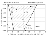
- FIG. 1 is a schematic diagram showing an example of an EUV exposure apparatus. Total content (atomic %) of nitrogen (N) and oxygen (O) (X-axis) at the inflection point x 1 of the second aspect of the protective film of the multilayer reflective film-coated substrate of the present embodiment, and the metal element FIG.
- FIG. 3 is a diagram for explaining the relationship between the content M of Em and the content A of the additive element Ea, a ratio A/M (Y axis).
- FIG. 3 is a diagram for explaining the relationship between (x 1 ) (Y axis).
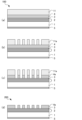
- FIG. 1 is a schematic cross-sectional view showing an example of a multilayer reflective film-coated substrate 90 of this embodiment.
- a substrate 90 with a multilayer reflective film shown in FIG. 1 includes a multilayer reflective film 2 and a protective film 3 on a substrate 1 .
- the protective film 3 has a first layer 32 and a second layer 34 in this order on the multilayer reflective film 2.
- the multilayer reflective film-coated substrate 90 can further include other thin films such as the back conductive film 5.
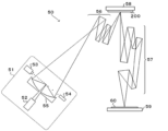
- FIG. 2 is a schematic cross-sectional view showing an example of the reflective mask blank 100 of this embodiment.
- a reflective mask blank 100 shown in FIG. 2 includes a multilayer reflective film 2 , a protective film 3 , and an absorber film 4 on a substrate 1 .
- the reflective mask blank 100 can have a back conductive film 5.
- the multilayer reflective film-coated substrate 90 can further include other thin films such as the resist film 11.
- FIG. 3 is a schematic cross-sectional view showing another example of the reflective mask blank 100.
- the reflective mask blank 100 shown in FIG. 3 further includes an etching mask film 6 on the absorber film 4.
- the reflective mask blank 100 can further include other thin films such as the resist film 11.
- arranging (forming) thin film B on thin film A (or substrate) means that thin film B is arranged (forming) in contact with the surface of thin film A (or substrate). It also includes cases where it means that there is another thin film C between the thin film A (or substrate) and the thin film B.
- the thin film B is arranged in contact with the surface of the thin film A (or the substrate) means that there is no intervening other thin film between the thin film A (or the substrate) and the thin film B.
- thin film A (or substrate) and thin film B are arranged so as to be in direct contact with each other.
- “above” does not necessarily mean the upper side in the vertical direction. “Above” merely indicates the relative positional relationship between the thin film and the substrate.
- This embodiment is a substrate 90 with a multilayer reflective film that includes a substrate 1, a multilayer reflective film 2 provided on the substrate 1, and a protective film 3 provided on the multilayer reflective film 2.
- the multilayer reflective film coated substrate 90 of this embodiment will be specifically described.
- the substrate 1 preferably has a low coefficient of thermal expansion within the range of 0 ⁇ 5 ppb/° C. in order to prevent distortion of the transferred pattern due to heat during exposure to EUV light.
- a material having a low coefficient of thermal expansion in this range for example, SiO 2 -TiO 2 glass, multi-component glass ceramics, etc. can be used.
- the main surface (first main surface) of the substrate 1 on the side on which the transfer pattern (absorber pattern 4a described below) is formed is preferably processed to improve flatness.
- the flatness is preferably 0.1 ⁇ m or less, more preferably 0.05 ⁇ m or less, particularly Preferably it is 0.03 ⁇ m or less.
- the second main surface (back surface) opposite to the side on which the transfer pattern is formed is a surface that is fixed to the exposure device by an electrostatic chuck.
- the flatness is 0.1 ⁇ m or less, more preferably 0.05 ⁇ m or less, particularly preferably 0.03 ⁇ m or less.
- flatness is a value representing surface warpage (deformation amount) indicated by TIR (Total Indicated Reading).
- TIR Total Indicated Reading
- Flatness (TIR) is defined as the plane determined by the least squares method with the surface of the substrate 1 as a reference, and the highest position of the surface of the substrate 1 above this focal plane and the substrate below the focal plane. This is the absolute value of the difference in height from the lowest position on the surface of 1.
- the surface roughness of the main surface of the substrate 1 on the side where the transferred pattern is formed is preferably 0.1 nm or less in terms of root mean square roughness (Rq). Note that the surface roughness can be measured using an atomic force microscope.
- the substrate 1 preferably has high rigidity in order to prevent the thin film (such as the multilayer reflective film 2) formed thereon from being deformed due to film stress.
- the thin film such as the multilayer reflective film 2
- those having a high Young's modulus of 65 GPa or more are preferred.
- the multilayer reflective film-coated substrate 90 of the embodiment includes the multilayer reflective film 2.
- the multilayer reflective film 2 provides the reflective mask 200 with a function of reflecting EUV light.
- the multilayer reflective film 2 is a multilayer film in which layers each containing elements having different refractive indexes as main components are periodically laminated.
- the multilayer reflective film 2 consists of a thin film of a light element or its compound (high refractive index layer), which is a high refractive index material, and a thin film (low refractive index layer) of a heavy element or its compound, which is a low refractive index material. ) are alternately stacked for about 40 to 60 periods.
- the multilayer film used as the multilayer reflective film 2 has a structure in which a high refractive index layer and a low refractive index layer are laminated in this order from the substrate 1 side, with one period having a laminated structure of high refractive index layer/low refractive index layer. can be. Further, the multilayer film may have a structure in which a low refractive index layer and a high refractive index layer are laminated in this order from the substrate 1 side, with one period having a laminated structure of a low refractive index layer/high refractive index layer. . Note that the outermost layer of the multilayer reflective film 2, that is, the surface layer of the multilayer reflective film 2 on the side opposite to the substrate 1 side, is preferably a high refractive index layer.
- the uppermost layer is It becomes a low refractive index layer.
- the low refractive index layer constitutes the outermost surface of the multilayer reflective film 2
- it will be easily oxidized, resulting in a decrease in the reflectance of the reflective mask 200. Therefore, it is preferable to form the multilayer reflective film 2 by further forming a high refractive index layer on the uppermost low refractive index layer.
- the high refractive index layer formed on the uppermost low refractive index layer can be the first layer 32 of the protective film 3 described later.
- the maximum The upper layer becomes a high refractive index layer. Therefore, in this case, there is no need to form an additional high refractive index layer.
- the uppermost high refractive index layer in this case can also serve as the first layer 32 of the protective film 3 described later.
- a layer containing silicon (Si) can be used as the high refractive index layer.
- materials containing Si in addition to Si alone, Si compounds containing boron (B), carbon (C), nitrogen (N), oxygen (O), and/or hydrogen (H) can be used. can.
- a high refractive index layer containing Si a reflective mask 200 with excellent reflectivity for EUV light can be obtained.
- a single metal selected from molybdenum (Mo), ruthenium (Ru), rhodium (Rh), and platinum (Pt), or an alloy thereof can be used as the low refractive index layer.
- the low refractive index layer is a molybdenum (Mo) layer and the high refractive index layer is a silicon (Si) layer.
- Mo molybdenum
- Si silicon
- the multilayer reflective film 2 for reflecting EUV light with a wavelength of 13 nm to 14 nm (for example, a wavelength of 13.5 nm) a Mo/Si periodic laminated film in which Mo layers and Si layers are alternately laminated for about 40 to 60 cycles is used. It can be preferably used.
- the low refractive index layer is a ruthenium (Ru) layer and the high refractive index layer is a silicon (Si) layer.
- Ru ruthenium
- Si silicon
- the multilayer reflective film 2 for reflecting EUV light with a wavelength of 13 nm to 14 nm (for example, a wavelength of 13.5 nm) an Ru/Si periodic laminated film in which Ru layers and Si layers are alternately laminated for about 30 to 40 periods is used. It can be preferably used.
- the reflectance of the multilayer reflective film 2 alone is usually 65% or more, and the upper limit is usually 73%.
- the film thickness and period of each constituent layer of the multilayer reflective film 2 can be appropriately selected depending on the exposure wavelength. Specifically, the film thickness and period of each constituent layer of the multilayer reflective film 2 can be selected so as to satisfy the Bragg reflection law.
- the film thicknesses of the high refractive index layers or the film thicknesses of the low refractive index layers do not necessarily have to be the same.
- the method for forming the multilayer reflective film 2 is known in the art.
- the multilayer reflective film 2 can be formed by forming each layer by, for example, ion beam sputtering.
- a Si film with a thickness of about 4 nm is first formed on the substrate 1 using a Si target, and then a Si film with a thickness of about 3 nm is formed using a Mo target.
- the multilayer reflective film 2 is formed by forming a Mo film of about 100 mL and laminating 40 to 60 cycles (the outermost layer is a Si film). Note that in the case of 60 cycles, the number of steps increases compared to 40 cycles, but the reflectance to EUV light can be increased.
- the multilayer reflective film coated substrate 90 of this embodiment has a predetermined protective film 3 on the multilayer reflective film 2.
- the absorber film 4 is etched to form the absorber pattern 4a. Since the protective film 3 has high etching resistance, damage to the surface of the multilayer reflective film 2 can be suppressed when the absorber film 4 is etched. Therefore, by providing a predetermined protective film 3 on the multilayer reflective film 2, damage to the surface of the multilayer reflective film 2 can be suppressed when manufacturing the reflective mask 200 using the multilayer reflective film coated substrate 90. Can be done. Therefore, the reflective mask 200 obtained has good reflectance characteristics with respect to EUV light.
- the predetermined protective film 3 that can be used for the multilayer reflective film coated substrate 90 of this embodiment is sometimes referred to as "the protective film 3 of this embodiment.”
- the protective film 3 of this embodiment includes a first layer 32 and a second layer 34.
- the first layer 32 is arranged between the second layer 34 and the multilayer reflective film 2 .
- the first layer 32 is a thin film that has the function of protecting the multilayer reflective film 2 from oxidation.
- the first layer 32 is part of the protective film 3.
- the first layer 32 can also serve as the top layer of the multilayer reflective film 2.
- the second layer 34 is a thin film having a function of having high resistance to the etching gas used for etching the absorber film 4.
- the second layer 34 needs to be a thin film that has high reflectance to EUV light and high etching resistance to etching gas.
- the multilayer reflective film coated substrate 90 is protected against EUV light by heat treatment in the manufacturing process of the reflective mask.
- a phenomenon in which the reflectance decreases may occur. The reason for this is thought to be that a predetermined element in the first layer 32 (an element that exhibits the function of the first layer 32) diffuses into the second layer 34.
- the surface of the first layer 32 (the interface between the first layer 32 and the second layer 34) is , nitriding and/or oxidizing.
- the adhesion between the first layer 32 and the second layer 34 is reduced. Knowledge has been obtained that problems arise. If the adhesion between the first layer 32 and the second layer 34 decreases, there is a risk that film peeling defects will occur.
- the protective film 3 of this embodiment includes at least one metal element Em and at least one additive element Ea. That is, the first layer 32 and the second layer 34 constituting the protective film 3 can contain the metal element Em and/or the additive element Ea. By containing the metal element Em, the protective film 3 of this embodiment can have high etching resistance against the etching gas of the absorber film 4. Moreover, the protective film 3 of this embodiment can improve the adhesion between the first layer 32 and the second layer 34 by including the additive element Ea. Therefore, the protective film 3 of this embodiment can suppress the occurrence of film peeling defects. In other words, the protective film 3 of this embodiment provides a substrate with a multilayer reflective film that can improve the adhesion between the first layer 32 and the second layer 34 while maintaining the high etching resistance of the protective film 3. You can get 90.
- the protective film 3 contains at least one metal element Em.
- the metal element Em is an element having a Fermi level of ⁇ 4.7 eV or less.
- the content (atomic %) of the metal element Em is indicated by the symbol "M”.
- the metal element Em is also referred to as the Em element.
- the metal element Em is an element (metal element) that functions as the protective film 3. Since the metal element Em has a Fermi level of -4.7 eV or less, it can be used in chlorine (Cl)-based gases, bromine (Br)-based gases, fluorine (F)-based gases, as well as nitrogen and /Or has low reactivity with gases containing oxygen as a constituent element. Therefore, when the metal element Em is used as a material for the protective film 3, deterioration of the material is less likely to occur, and the function of the protective film 3 is less likely to deteriorate.
- the Fermi level of a certain element refers to the value of the energy of the Fermi level of a pure substance of a single element when the vacuum level is the origin (zero).
- the Fermi level of a metal material can be energy with a negative work function value.
- the metal element Em is Ru
- the work function of a pure substance of Ru element is 4.7 eV
- the Fermi level of Ru is ⁇ 4.7 eV.
- the metal element Em can be an element having a Fermi level lower than the Fermi level of Ru. It is known that Ru can be preferably used as an element constituting the protective film 3. Therefore, by using an element (metallic element) having a Fermi level that is the same as or lower than the Fermi level of Ru (Fermi level with a large negative value), a thin film with high etching resistance can be obtained. .
- elements having a Fermi level lower than the Fermi level of Ru include Ru, Tc, Os, Co, Re, Rh, Pd, Au, Ni, Ir, and Pt. At least one selected from these elements can be used as the metal element Em.
- the metal element Em included in the protective film 3 of this embodiment is preferably one or more elements selected from ruthenium (Ru), rhodium (Rh), and iridium (Ir).
- the metal element Em included in the protective film 3 of this embodiment can be made of only one or more elements selected from ruthenium (Ru), rhodium (Rh), and iridium (Ir). By using these elements, it is possible to more reliably obtain the protective film 3 having high etching resistance while maintaining high reflectance.
- the etching resistance of the protective film 3 can be improved.
- the protective film 3 contains Ru as the metal element Em the optical characteristics of the protective film 3 can be appropriately adjusted.
- the protective film 3 includes at least one additive element Ea.
- the additive element Ea is an element having a Fermi level exceeding ⁇ 4.7 eV.
- the content (atomic %) of the additive element Ea is indicated by the symbol "A”.
- the additive element Ea is also referred to as Ea element.
- the adhesion between the first layer 32 and the second layer 34 that constitute the protective film 3 can be improved. Since the additive element Ea is an element having a Fermi level exceeding ⁇ 4.7 eV, it has high reactivity with other elements. Therefore, when the protective film 3 contains the additive element Ea, it can contribute to improving the adhesion between the first layer 32 and the second layer 34.
- the additive element Ea can be an element having a Fermi level higher than the Fermi level of Cu.
- Cu can be used as an element that can improve the adhesion between two types of thin films. Therefore, by using an element having a Fermi level equal to or higher than the Fermi level of Cu (a Fermi level with a small negative value), the first layer 32 and the second layer 34 can be closely bonded. It can contribute to improving sexual performance.
- the additive elements Ea contained in the protective film 3 of this embodiment include Tl, Hf, Ti, Zr, Y, Mn, In, Ga, Cd, Bi, Ta, Pb, Ag, Al, V, Nb, Sn, and Zn. , Hg, Cr, Fe, Sb, W, Mo, and Cu.
- the additive elements Ea contained in the protective film 3 of this embodiment include Tl, Hf, Ti, Zr, Y, Mn, In, Ga, Cd, Bi, Ta, Pb, Ag, Al, V, Nb, Sn, and Zn. , Hg, Cr, Fe, Sb, W, Mo, and Cu.
- the additive element Ea included in the protective film 3 of this embodiment is at least one selected from Ti, Zr, Ta, Nb, and Cr. Moreover, it is more preferable to use at least one selected from Ta, Nb, and Cr as the additive element Ea included in the protective film 3 of this embodiment. By using these elements, it is possible to improve the adhesion between the first layer 32 and the second layer 34 and to improve the cleaning resistance.
- Cr When nitrogen is included near the surface of the first layer 32 (the interface between the first layer 32 and the second layer 34), Cr may be used as the additive element Ea included in the protective film 3 of this embodiment. is even more preferable. This is because Cr, when nitrided, lowers the extinction coefficient, alleviates the absorption of EUV light, and can contribute to improving the reflectance. On the other hand, when Hf, Ti, Zr, Y, V, and Nb are nitrided, they tend to increase the extinction coefficient, strengthen the absorption of EUV light, and lower the reflectance.
- Hf, V, and Cr When oxygen is included near the surface of the first layer 32 (the interface between the first layer 32 and the second layer 34), Hf, V, and It is preferable to use at least one selected from Cr. This is because when Hf, V, and Cr are oxidized, they can lower the extinction coefficient, alleviate absorption of EUV light, and contribute to improving the reflectance. On the other hand, when Ti, Zr, Y, and Nb are nitrided, they tend to increase the extinction coefficient, strengthen the absorption of EUV light, and lower the reflectance.
- the metal element Em can be included in both the first layer 32 and the second layer 34. That is, if the metal element Em can exist at the interface between the first layer 32 and the second layer 34, the metal element Em can be added when forming the first layer 32. , or the metal element Em can be added during the second layer 34. Further, the metal element Em can be added when forming both the first layer 32 and the second layer 34.
- the first layer 32 of the protective film 3 of this embodiment can be disposed on the multilayer reflective film 2 and in contact with the multilayer reflective film 2 .
- the first layer 32 is a thin film that is part of the protective film 3 for protecting the multilayer reflective film 2 from oxidation.
- the material for the first layer 32 is not particularly limited as long as it can protect the multilayer reflective film 2 from oxidation.
- Materials for the first layer 32 include materials containing silicon (Si) (for example, Si, SiN, SiO, SiON, and SiC), and materials containing boron (B) and carbon (C) (for example, B 4 C). Examples include.
- the first layer 32 is, for example, a thin film formed under conditions of only silicon (Si), a thin film formed under conditions of only SiN, or a thin film formed under conditions of only B 4 C. It can be a thin film. Note that when the uppermost layer of the multilayer reflective film 2 is a high refractive index layer, the uppermost high refractive index layer can also serve as the first layer 32 of the protective film 3.
- a thin film formed under conditions such that it consists only of silicon (Si) "a thin film formed under conditions such that it consists only of SiN", or “a thin film formed under conditions consisting only of B 4 C”
- the first layer 32 which is a "thin film formed under conditions consisting only of silicon (Si)"
- silicon (Si) diffused from other layers after the first layer 32 is formed. ) will contain elements other than .
- a thin film formed under conditions in which the elements of other thin films diffuse into the first layer 32 from the thin film in the vicinity of the first layer 32, and is made of only a predetermined element is generally contains elements other than the predetermined elements. Therefore, a thin film formed under conditions in which it consists only of silicon (Si) can be a thin film containing Si.
- a thin film formed under conditions such that it consists only of SiN can be a thin film containing SiN.
- a thin film formed under conditions such that it consists only of B 4 C can be a thin film containing B 4 C.
- the first layer 32 of the protective film 3 of this embodiment can be formed by various known methods, such as ion beam sputtering, sputtering, reactive sputtering, vapor deposition (CVD), and vacuum evaporation. It is.
- the first layer 32 is a thin film formed under conditions such that it is made only of silicon (Si), only silicon (Si) is formed when forming the first layer 32. It is possible to form a film under certain conditions.
- the first layer 32 can be formed by ion beam sputtering using a Si target.
- the first layer 32 is a thin film formed only of SiN
- the first layer 32 may be formed using a Si target in a nitrogen gas atmosphere, for example. This can be performed by magnetron sputtering method (reactive sputtering method).
- the first layer 32 is a thin film formed under conditions such that it consists only of B 4 C, for example, the first layer 32 may be formed using a target containing B and C in a predetermined composition. It can be performed by using an ion beam sputtering method.
- the first layer 32 can be a thin film formed under conditions that include the additive element Ea.
- the first layer 32 can be a thin film containing Si, SiC and/or B 4 C and an additive element Ea.
- the first layer 32 can include an additive element Ea.
- the first layer 32 can further include at least one selected from nitrogen (N) and oxygen (O) in a thin film containing Si, SiC and/or B 4 C, and the additive element Ea.
- the first layer 32 preferably contains nitrogen (N) and/or oxygen (O) near the interface with the second layer 34.
- nitrogen (N) and/or oxygen (O) in the first layer 32 are high, elements in the first layer 32 (e.g., silicon (Si)) diffuse into the second layer 34. can be restrained from doing so. As a result, it is possible to suppress a decrease in the reflectance of the second layer 34 due to diffusion of the elements of the first layer 32.
- the film formation of the first layer 32 or the second layer 34 is performed using nitrogen gas and/or This can be performed by a DC magnetron sputtering method (reactive sputtering method) in an oxygen gas atmosphere.
- a decrease in the reflectance of the second layer 34 due to diffusion of the elements of the first layer 32 can be suppressed.
- oxygen (O) it is preferable to introduce oxygen (O) to increase the concentration of nitrogen (N) and/or the concentration of oxygen (O) at the interface between the first layer 32 and the second layer 34.
- concentration of nitrogen (N) and/or the concentration of oxygen (O) at the interface between the first layer 32 and the second layer 34 becomes too high, the reflectance will decrease and the adhesion will deteriorate. , it is necessary to have a predetermined concentration. This point will be discussed later.
- the second layer 34 of the protective film 3 of this embodiment is disposed on and in contact with the first layer 32 .
- the second layer 34 can be a thin film that functions as the protective film 3 by increasing the resistance of the protective film 3 to etching gas and to cleaning.
- the second layer 34 contains the above-mentioned metal element Em.
- the second layer 34 can be a thin film formed under conditions that include the metal element Em.
- the content of the metal element Em in the second layer 34 is greater than the content of the metal element Em in the first layer 32. This is because the second layer 34 needs to be a thin film with high etching resistance.
- the metal element Em contained in the second layer 34 is preferably one or more elements selected from ruthenium (Ru), rhodium (Rh), and iridium (Ir). By using these elements, it is possible to obtain the second layer 34 having high etching resistance while maintaining high reflectance.
- the second layer 34 can be a thin film formed under conditions that include the additive element Ea.
- the second layer 34 can include an additive element Ea. Since the second layer 34 contains the additive element Ea, the additive element Ea can be present at the interface between the first layer 32 and the second layer 34. As a result, the adhesion between the first layer 32 and the second layer 34 can be improved.
- the second layer 34 can be a thin film formed under conditions that include the metal element Em and the additive element Ea.
- the second layer 34 can include both the metal element Em and the additive element Ea. Since the second layer 34 contains the metal element Em, it is possible to obtain the second layer 34 having high etching resistance. Furthermore, by including the additive element Ea in the second layer 34, it is possible to more reliably improve the adhesion between the first layer 32 and the second layer 34.
- a thin film formed under conditions that include the metal element Em or "a thin film formed under conditions that include an additive element Ea” refers to the first layer. 32, it means a thin film formed under conditions for forming a thin film containing the metal element Em, or a thin film formed under conditions for forming a thin film containing the additive element Ea.
- elements other than those forming the second layer 34 may diffuse from the first layer 32 to the second layer 34 .
- a thin film formed under conditions that include the metal element Em may contain an element (for example, silicon) that diffuses from the first layer 32 to the second layer 34 after the first layer 32 is formed. (Si)).
- a thin film formed under conditions that contains a predetermined element by diffusing elements from other thin films from the thin film near the second layer 34 to the second layer 34 generally , contains elements other than the predetermined elements.
- the content of the metal element Em in the second layer 34 is preferably 40 to 95 atomic %, more preferably 50 to 90 atomic %.
- the content of the additive element Ea in the second layer 34 is preferably 1 to 10 atomic %, more preferably 2 to 8 atomic %.
- the second layer 34 can further include at least one selected from nitrogen (N) and oxygen (O).
- the second layer 34 can be a thin film formed under conditions that include the metal element Em, the additive element Ea, and at least one selected from nitrogen (N) and oxygen (O).
- the second layer 34 can be a thin film formed under conditions such that it contains only at least one selected from the metal element Em, the additive element Ea, nitrogen (N), and oxygen (O).
- the content of nitrogen (N) and/or oxygen (O) in the second layer 34 is preferably low.
- elements in the first layer 32 for example, silicon (Si)
- the effective film of the second layer 34 that functions as the protective film 3 is reduced. It is possible to suppress the thickness from becoming thinner.
- the second layer 34 contains nitrogen (N) and/or oxygen (O) near the interface with the first layer 32.
- the second layer 34 of the protective film 3 of this embodiment can be formed by various known methods, such as ion beam sputtering, sputtering, reactive sputtering, vapor deposition (CVD), and vacuum evaporation. It is.
- the second layer 34 of the protective film 3 of this embodiment is preferably formed by magnetron sputtering (reactive sputtering) in a nitrogen gas atmosphere.
- the target for example, a single metal target or an alloy target of the metal component (metal element, for example, metal element Em and/or additive element Ea) contained in the second layer 34 can be used.
- the second layer 34 is formed by a reactive sputtering method, the second layer 34 can be continuously formed in a nitrogen gas atmosphere after the first layer 32 is formed.
- the formation of the second layer 34 is , for example, a DC magnetron sputtering method (reactive sputtering method) in a nitrogen (N) gas and/or oxygen (O) gas atmosphere using an alloy target of at least one metal element Em and at least one additional element Ea. This can be done by
- the second layer 34 having a predetermined composition distribution is formed by changing the film forming conditions such as the flow rate (pressure) of nitrogen gas and/or the applied power. Can be done. However, when appropriate film formation conditions are selected, even if the film formation conditions are kept constant, the second layer 34 with a predetermined composition distribution may be caused by the diffusion of elements within the second layer 34. can be formed into a film. For example, when obtaining the second layer 34 containing silicon (Si), even if the second layer 34 is formed under conditions that do not contain silicon (Si), after the film formation, By diffusing silicon (Si) from the first layer 32, a second layer 34 containing silicon (Si) can be obtained.
- the second layer 34 is formed continuously after the first layer 32 is formed, without being taken out of the film forming apparatus into the atmosphere. If the first layer 32 is taken out into the atmosphere from the film forming apparatus after being formed, the surface of the first layer 32 may be excessively oxidized or contaminated with unexpected elements. be. In addition, when the surface of the first layer 32 is covered with a nitride film, the adhesion between the first layer 32 and the second layer 34 is better and the reflectance is higher than when covered with an oxide film. There is a tendency to Therefore, it is better to cover the surface of the first layer 32 with a nitride film rather than with an oxide film.
- the first layer 32 and the second layer 34 are deposited in the atmosphere from a deposition apparatus. It is preferable to carry out the process continuously without taking it out at any time.
- the protective film 3 of this embodiment includes a first layer 32 and a second layer 34.
- a first layer 32 is formed on the multilayer reflective film 2 and a second layer 34 is formed on the first layer 32.
- the second layer 34 can be formed in contact with the first layer 32.
- the elements contained in the first layer 32 typically diffuse into the second layer 34. Additionally, the elements contained in the second layer 34 typically diffuse into the first layer 32. In this way, the elements contained in the first layer 32 and the second layer 34 typically interdiffuse.
- the present inventors found that the elements (components) of the first layer 32 and the second layer 34 interdiffused. It has been found that the predetermined content distribution of the components contained in the protective film 3 with respect to the position x in the film thickness direction is related to the adhesion between the first layer 32 and the second layer 34, and the present invention reached.
- the predetermined content distribution of the components in the protective film 3 of this embodiment is defined as the distribution in the thickness direction (depth direction) of the protective film 3 with the film thickness direction (depth direction) of the protective film 3 as the x axis. direction) is the position x, the position x where the component is dominant in the second layer 34 and the component is dominant in the first layer 32 is the inflection point x1 , and the content of the metal element Em is M.
- the distribution is such that the ratio A/M at the inflection point x1 is 0.020 or more, where A is the content of the additive element Ea.
- the x-axis which is the film thickness direction (depth direction) of the protective film 3, is directed from the surface of the protective film 3 on which the absorber film is formed toward the interface between the protective film 3 and the multilayer reflective film.
- the direction can be the direction in which the value of x increases.
- the content distribution of the components contained in the protective film 3 (the first layer 32 and the second layer 34) with respect to the position x in the film thickness direction of the protective film 3 of this embodiment can be determined using, for example, a scanning transmission electron microscope (STEM). It can be measured by energy dispersive X-ray spectroscopy (EDX). Note that the content distribution can also be measured using other analysis methods, such as X-ray photoelectron spectroscopy (XPS). By specifying the components (elements) contained in the first layer 32 and the second layer 34 and measuring the content of each component with respect to the position x in the film thickness direction of the protective film 3, each The content distribution of the components can be obtained.
- STEM scanning transmission electron microscope
- EDX energy dispersive X-ray spectroscopy
- XPS X-ray photoelectron spectroscopy
- the state of a reflective mask blank having the absorber film 4 on the protective film 3, or the absorber film 4 and the etching mask film 6, or the reflection after patterning the absorber film 4 is measured.
- the composition of each layer may be determined by measuring the state of the mold mask.
- y(x) may be simply referred to as a "distribution ratio.”
- y(x) (total content of components in the first layer 32 at position x)/(total content of components in the first layer 32 and second layer 34 at position x)
- the first layer 32 is a thin film formed under conditions that include silicon (Si), nitrogen (N), and oxygen (O)
- the second layer 34 is a thin film that contains Ru (metallic element Em)
- the distribution ratio y(x) is as follows. become. Nitrogen (N) and oxygen (O) are included in both the first layer 32 and the second layer 34, but do not need to be summed twice in the denominator of the equation below.
- y(x) (total content of Si content, N content and O content at position x)/(Si content, N content, O content, Ru content, Rh content and Total content of Cr content)
- the first layer 32 is a thin film formed under conditions that include Si, and is not a thin film formed under conditions that include Ru, Rh, and Cr. . Therefore, as a component of the first layer 32, Si is selected, and Ru, Rh, and Cr are not selected.
- the second layer 34 is a thin film formed under conditions that include Ru, Rh, and Cr, but not a thin film formed under conditions that include Si. Therefore, Ru, Rh, and Cr are selected as the components of the second layer 34, and Si is not selected.
- nitrogen (N) and oxygen (O), which are gases at room temperature, may be contained in the first layer 32 and the second layer 34.
- the components of the first layer 32 may include nitrogen (N) and/or oxygen ( O). Further, the distribution ratio y(x) can be determined not only by the film forming conditions but also by taking into account the content distribution as a result of measurement.
- the analysis sample is analyzed using a focused ion beam (FIB) or the like. It is necessary to process it into a rectangle. At this time, a conductive protective film made of carbon (C) and/or platinum (Pt) is formed to prevent the sample surface from being damaged by the ion beam.
- carbon (C) may re-deposit on the cross-section of the processed sample and be included in the quantitative value as part of the constituent components of the analysis sample. It can be excluded from the components of the first layer 32 and the second layer 34 to obtain y(x).
- the components of the first layer 32 As, carbon (C) can be included.
- an inflection point x1 which is a position x where the component of the second layer 34 is dominant to the component of the first layer 32.
- the inflection point x1 can be an inflection point when the distribution ratio y(x) of a predetermined component is curve-fitted with a predetermined function.
- the inflection point x 1 can be considered to be the position of the interface between the first layer 32 and the second layer 34 .
- the elements (components) of the first layer 32 and the second layer 34 normally diffuse into each other, it is difficult to specify the interface between the first layer 32 and the second layer 34. It is.
- the interface between the first layer 32 and the second layer 34 can be specified.
- the position of the inflection point x1 may be referred to as the interface between the first layer 32 and the second layer 34.
- the inflection point x1 can be found as follows.
- the range of x for curve fitting the distribution ratio y(x) of a predetermined component to the position x in the film thickness direction of the protective film 3 using a predetermined function is determined.
- the range of x for curve fitting the distribution ratio y(x) can be determined as follows. Note that, below, a function subjected to curve fitting will also be expressed as a distribution ratio y(x).
- a sigmoid-type function can be used as a function for curve fitting the distribution ratio y(x).
- a sigmoid-type function is generally used to approximate a sigmoid-shaped profile.
- the sigmoid function a higher-order function of cubic function or higher, an error function, an exponential function, a sine function, or the like can be used.
- a quartic function shown in equation (1) can be used as a function for curve fitting the distribution ratio y(x), for example, a quartic function shown in equation (1) can be used.
- a, b, c, d and e are constants.
- y(x) ax4 + bx3 + cx2 +dx+e...(1)
- the range of x (starting point and ending point of x) for curve fitting the distribution ratio y(x) using a predetermined function is determined.
- the total content (atomic %) of Em elements and Ea elements decreases from the maximum value, and is 5 atomic % or more and 20 atomic %.
- the position (depth) where the coefficient of determination R2 of curve fitting by a predetermined function becomes the maximum value in the range of x can be set.
- a predetermined function obtained by curve fitting the distribution ratio y(x) is second-order differentiated to obtain a second-order derivative y''(x).
- the distribution ratio y(x) is curve fitted with a cubic function, and the linear function of the second derivative obtained by second-order differentiation of the cubic function is 4, which is closer to the value of x of the solution where the linear function is zero.
- the inflection point x1 obtained as described above indicates the position x (depth in the film thickness direction of the protective film 3) at which the component dominance of the second layer 34 switches to the component dominance of the first layer 32. become.
- the ratio A/M at the inflection point x1 is 0.020 or more, preferably 0.022 or more.
- the protective film 3 includes a plurality of metal elements Em
- the content M of the metal elements Em is the total content (atomic %) of the plurality of metal elements Em.
- the protective film 3 includes a plurality of additive elements Ea
- the content A of the additive elements Ea is the total content (atomic %) of the plurality of additive elements Ea.
- the protective film 3 of this embodiment in which the ratio A/M at point x1 is 0.020 or more may be referred to as a first aspect of the protective film 3 of this embodiment.
- the inflection point x 1 corresponds to the interface between the first layer 32 and the second layer 34 . Since the ratio A/M at the inflection point This means that the additional element Ea exists in an amount greater than or equal to the amount of the additive element Ea. Since the protective film 3 of this embodiment has such a content distribution of the metal element Em and the additive element Ea, it is possible to improve the adhesion between the first layer 32 and the second layer 34. can.
- the ratio A/M at the inflection point x1 is preferably less than 0.17, more preferably 0.16 or less, and 0.12. It is more preferable that it is the following.
- the upper limit of the ratio A/M it is possible to suppress an adverse effect on the reflectance of the multilayer reflective film-coated substrate 90 due to the content A of the additive element Ea being too large. can.
- the value at x 1 of the first derivative y'(x) of y(x) means the slope of y(x) at position x 1 .
- the slope (y'(x 1 )) of y(x) at position x 1 can be expressed by the following equation (4).
- y'(x 1 ) 4ax 1 3 +3bx 1 2 +2cx 1 +d...(4)
- the slope y'(x 1 ) is, the steeper the composition change at the interface between the first layer 32 and the second layer 34 is. This means that the degree of diffusion of components (elements) is small.
- the slope y'(x 1 ) of the distribution ratio y(x) is large.
- the content A of the additive element Ea at the inflection point x1 is preferably 1 atomic % or more and 15 atomic % or less, and 1.5 atomic %. More preferably, the content is 10 atomic % or less.
- the content M of the metal element Em at the inflection point x1 is preferably 5 atomic % or more and 80 atomic % or less, and 10 atomic % or more and 75 atomic % or more. More preferably, it is at most atomic %.
- the first layer 32 includes silicon (Si) and at least one selected from nitrogen (N) and oxygen (O), and The total content of nitrogen (N) and oxygen (O) at point x 1 is preferably 2 atomic % or more, more preferably 4 atomic % or more.
- the content of nitrogen (N) and oxygen (O) is equal to or higher than a predetermined amount, so that the first layer 32 Adverse effects caused by diffusion of component elements (for example, Si) into the second layer 34 can be suppressed.
- the total content of nitrogen (N) and oxygen (O) at the inflection point x 1 of the protective film 3 of the substrate 90 with a multilayer reflective film of this embodiment is 35 atomic % or less, and 30 atomic %. It is more preferable that it is below. If the content of nitrogen (N) and/or oxygen (O) at the interface between the first layer 32 and the second layer 34 is too large, the content at the interface between the first layer 32 and the second layer 34 may be too high. Film peeling may occur. Therefore, it is preferable that the total content of nitrogen (N) and oxygen (O) at the inflection point x1 is equal to or less than a predetermined amount.
- the thickness of the first layer 32 is preferably 1.0 to 2.0 nm, more preferably 1.2 to 1.5 nm. Further, the thickness of the second layer 34 is preferably 1.5 to 5.0 nm, more preferably 2.0 to 4.0 nm.
- the film thickness of the first layer 32 and the second layer 34 described above is the film thickness when it is assumed that the interface between the first layer 32 and the second layer 34 is located at the above-mentioned inflection point x1 . It is thick.
- the total thickness of the protective film 3 including the first layer 32 and the second layer 34 (sometimes simply referred to as "thickness of the protective film 3") is the function of the protective film 3. There is no particular restriction as long as it can fulfill the following requirements. From the viewpoint of reflectance of EUV light, the thickness of the protective film 3 is preferably from 1.0 nm to 8.0 nm, more preferably from 1.5 nm to 6.0 nm.
- the content of the components (metal element Em, additive element Ea, etc.) contained in the first layer 32 and the second layer 34 described above changes continuously in the film thickness direction (depth direction) of each layer.
- the content can be such that there is a compositional gradient.
- heat treatment can be performed after forming the protective film 3 or after forming the absorber film 4 to obtain the reflective mask blank 100.
- heating can be performed at a temperature higher than the pre-baking temperature (about 110° C.) of the resist film 11 in the manufacturing process of the reflective mask blank 100.
- the temperature conditions for the heat treatment are usually 130°C or more and 300°C or less, preferably 150°C or more and 250°C or less.
- the protective film 3 of this embodiment can further include layers other than the first layer 32 and second layer 34 described above, if necessary.
- the second layer 34 having a composition more preferable for promoting the diffusion of nitrogen contained in the second layer 34 and suppressing the diffusion of Si into the second layer 34 is obtained. There are cases where it is possible.
- the protective film 3 of the second aspect of the present embodiment includes a first layer 32 and a second layer 34 similarly to the first aspect described above.
- the protective film 3 of the second embodiment has an inflection point x 1 , which is the position x where the component of the second layer 34 is dominant to the component of the first layer 32, as in the above embodiment.
- the ratio A/M at the inflection point x 1 and the inflection point The specific relationship is the total content (atomic %) of nitrogen (N) and oxygen (O) in x 1 .
- the protective film 3 of the second aspect of this embodiment contains nitrogen (N) and/or oxygen (O).
- FIG. 6 shows the total content (atomic %) of nitrogen (N) and oxygen (O) at the inflection point x 1 (X axis) and the metal element Em of the second aspect of the protective film 3 of this embodiment.
- FIG. 3 is a diagram for explaining the relationship between the content M of the additive element Ea and the content A of the additive element Ea, the ratio A/M (Y axis).
- the shaded area between the straight line of equation (2-1) and the straight line of equation (2-2) in Figure 6 is and Y area. Note that, for reference, the X and Y values of Examples 1 to 10, which will be described later, are plotted in FIG.
- Y which is the ratio A/M, is greater than or equal to zero (Y ⁇ 0). This is because the content M of the metal element Em and the content A of the additional element Ea never take negative values.
- the Fermi level is relatively large for the additive element Ea, becomes smaller in the order of the metal element Em and silicon nitride, and is the smallest for silicon oxide. Therefore, the Fermi level of the material containing nitrogen (N) and/or oxygen (O) is relatively small compared to the Fermi level of the additive element Ea and the metal element Em.
- the Fermi level is relatively large for the additive element Ea, becomes smaller in the order of the metal element Em and silicon nitride, and is the smallest for silicon oxide. Therefore, the Fermi level of the material containing nitrogen (N) and/or oxygen (O) is relatively small compared to the Fermi level of the additive element Ea and the metal element Em.
- the protective film 3 of the second aspect of the present embodiment satisfies the above formulas (2-1) and (2-2), so that the protective film 3 at the interface between the first layer 32 and the second layer 34 is Diffusion of components (elements) into each other's layers is less likely to occur, and desired adhesion can be obtained at the interface between the first layer 32 and the second layer 34.
- the multilayer reflective film coated substrate 90 including the protective film 3 of the second aspect of the present embodiment can have the following configuration.
- the multilayer reflective film coated substrate 90 including the protective film 3 of the second aspect of the present embodiment includes: A substrate with a multilayer reflective film, comprising a substrate, a multilayer reflective film provided on the substrate, and a protective film provided on the multilayer reflective film,
- the protective film includes a first layer and a second layer, the first layer is disposed between the second layer and the multilayer reflective film,
- the protective film includes at least one metal element Em and at least one additional element Ea, and the content of the metal element Em in the second layer is lower than the content of the metal element Em in the first layer.
- the metal element Em is an element having a Fermi level of ⁇ 4.7 eV or less
- the additional element Ea is an element having a Fermi level of more than ⁇ 4.7 eV
- the protective film further includes at least one selected from nitrogen (N) and oxygen (O), In the content distribution of the components contained in the protective film with respect to the position x in the film thickness direction of the protective film, the position x at which the component of the second layer switches to the dominant component of the first layer is defined as an inflection point x.
- the content of the metal element Em is M
- the content of the additional element Ea is A
- the ratio A/M is Y
- X Y
- Y which is the ratio A/M at the inflection point x1
- X are, Y ⁇ -0.0233X+0.14...(2-1) and Y ⁇ 0.0096X-0.144 (2-2)
- This is a substrate with a multilayer reflective film characterized by the following relationship.
- the protective film 3 of the third aspect of the present embodiment includes a first layer 32 and a second layer 34 similarly to the first aspect and the second aspect described above.
- the protective film 3 of the third embodiment has an inflection point x 1 , which is the position x where the component of the second layer 34 is dominant to the component of the first layer 32, as in the above-described embodiments.
- the protective film 3 of the third embodiment has a distribution ratio y(x 1 ) at the inflection point x 1 (total content of the components of the first layer 32 at the inflection point x 1 / at the inflection point x 1
- the total content of the components of the first layer 32 and the second layer 34) and the slope y'(x 1 ) of the distribution ratio y(x 1 ) at the inflection point x 1 have a specific relationship. .
- FIG . 7 shows the distribution ratio y(x 1 ) (X axis) at the inflection point x 1 and the distribution ratio y(x 1 ) at the inflection point x 1 of the third aspect of the protective film 3 of this embodiment.
- FIG. 2 is a diagram for explaining the relationship between the slope y'(x 1 ) (Y axis).
- the region to the left of the straight line of equation (3) in FIG. 7 is the region of X and Y that satisfies the relationship of equation (3).
- the values of X and Y of Examples 1 to 10 described later are plotted for reference, and Examples 1 to 5, 7, 9, and 10 satisfy the condition of formula (3). ing.
- the protective film 3 of the third embodiment includes a first layer 32 and a second layer 34, but under such an exposure environment, the closer the compositions of the first layer 32 and the second layer 34 are ( (hereinafter referred to as "high homogeneity"), a phenomenon in which hydrogen permeates from the second layer 34 to the first layer 32 is likely to occur.
- the homogeneity of the first layer 32 and the second layer 34 depends on the distribution ratio y(x 1 ) at the inflection point x 1 , and the larger the distribution ratio y(x 1 ), the more the homogeneity becomes This makes it easier for hydrogen to permeate to the first layer 32.
- the rate of change in the distribution ratio at the inflection point x 1 that is, the slope y'(x 1 )
- the properties of the first layer 32 and the second layer 34 become clearly separated.
- the decreasing tendency of EUV reflectance due to long-term exposure shows a negative correlation with the distribution ratio y(x 1 ) and a positive correlation with y'(x 1 ). That is, as y(x 1 ) increases, the EUV reflectance tends to decrease more easily, and as y'(x 1 ) increases, the EUV reflectance tends to decrease less easily.
- the present inventors found that it is necessary to satisfy the above equation (3) in order to control the decrease in EUV reflectance due to long-term exposure to a desired level or less. I discovered something.
- the protective film 3 of the third aspect of the present embodiment makes it difficult for hydrogen to permeate from the second layer 34 to the first layer 32, so that the protective film 3 can be used for a long period of time. Decrease in EUV reflectance due to exposure can be made less likely to occur.
- the multilayer reflective film-coated substrate 90 including the protective film 3 of the third aspect of the present embodiment can have the following configuration.
- the multilayer reflective film coated substrate 90 including the protective film 3 of the third aspect of the present embodiment is A substrate with a multilayer reflective film, comprising a substrate, a multilayer reflective film provided on the substrate, and a protective film provided on the multilayer reflective film,
- the protective film includes a first layer and a second layer, the first layer is disposed between the second layer and the multilayer reflective film,
- the protective film includes at least one metal element Em and at least one additional element Ea, and the content of the metal element Em in the second layer is lower than the content of the metal element Em in the first layer.
- the metal element Em is an element having a Fermi level of ⁇ 4.7 eV or less
- the additional element Ea is an element having a Fermi level of more than ⁇ 4.7 eV
- the position x at which the component of the second layer switches to the dominant component of the first layer is defined as an inflection point x.
- the multilayer reflective film-coated substrate 90 of this embodiment can have a back conductive film 5 for electrostatic chuck.
- the back conductive film 5 is on the second main surface (back main surface) of the substrate 1 (on the side opposite to the surface on which the multilayer reflective film 2 is formed), and an intermediate layer such as a hydrogen intrusion suppressing film is formed on the substrate 1. (in some cases, on top of the intermediate layer).
- the sheet resistance required for the back conductive film 5 is usually 100 ⁇ /square or less.
- the method for forming the back conductive film 5 is, for example, a magnetron sputtering method or an ion beam sputtering method using a target of metal such as chromium or tantalum, or an alloy thereof.
- the material containing chromium (Cr) of the back conductive film 5 is preferably a Cr compound containing at least one selected from boron, nitrogen, oxygen, and carbon in Cr. Examples of the Cr compound include CrN, CrON, CrCN, CrCON, CrBN, CrBON, CrBCN, and CrBOCN.
- the material containing tantalum (Ta) for the back conductive film 5 may be Ta (tantalum), an alloy containing Ta, or a Ta compound containing at least one of boron, nitrogen, oxygen, and carbon in any of these.
- TA compounds include, for example, TAB, TAN, TAO, TAON, TACON, TABO, TABO, TABON, TABON, TABON, TAHFON, TAHFON, TAHFON, TAHFON, TAHFCON, TAHFCON, T some To mention TASION, TASICON, etc. can.
- the thickness of the back conductive film 5 is not particularly limited as long as it satisfies its function as an electrostatic chuck, but is usually from 10 nm to 200 nm. Further, this back conductive film 5 also serves to adjust the stress on the second main surface side of the mask blank 100. That is, the back conductive film 5 is adjusted to balance stress from various films formed on the first main surface side so that a flat reflective mask blank 100 can be obtained.
- the multilayer reflective film-coated substrate 90 does not necessarily need to include the back conductive film 5.
- the back conductive film 5 can be formed on the reflective mask blank 100.
- the reflective mask blank 100 of this embodiment will be explained. As shown in FIG. 2, the reflective mask blank 100 of this embodiment has an absorber film 4 on the protective film 3 of the multilayer reflective film-coated substrate 90 described above.
- the absorber film 4 of the reflective mask blank 100 of this embodiment is formed on the protective film 3.
- the basic function of the absorber film 4 is to absorb EUV light.
- the absorber film 4 may be an absorber film 4 aimed at absorbing EUV light, or may be an absorber film 4 having a phase shift function that takes into account the phase difference of EUV light.
- the absorber film 4 having a phase shift function absorbs EUV light and reflects a portion of the EUV light to shift the phase. That is, in the reflective mask 200 patterned with the absorber film 4 having a phase shift function, the portion where the absorber film 4 is formed absorbs and attenuates EUV light at a level that does not adversely affect pattern transfer. to reflect some of the light.
- the EUV light is reflected from the multilayer reflective film 2 via the protective film 3. Therefore, there is a desired phase difference between the reflected light from the absorber film 4 having a phase shift function and the reflected light from the field section.
- the absorber film 4 having a phase shift function is formed so that the phase difference between the light reflected from the absorber film 4 and the light reflected from the multilayer reflective film 2 is from 170 degrees to 260 degrees.
- the image contrast of the projected optical image is improved by the interference of the light beams with reversed phase differences at the pattern edge portion. As the image contrast improves, the resolution increases, and various latitudes regarding exposure such as exposure latitude and focus latitude can be increased.
- the absorber film 4 may be a single layer film or a multilayer film consisting of a plurality of films (for example, a lower absorber film (buffer layer) and an upper absorber film).
- a single layer film the number of steps during mask blank manufacturing can be reduced and production efficiency is increased.
- the optical constants and film thickness of the upper absorber film can be appropriately set so that it serves as an antireflection film during mask pattern defect inspection using light. This improves the inspection sensitivity when inspecting mask pattern defects using light.
- O oxygen
- N nitrogen
- the absorber film 4 By making the absorber film 4 a multilayer film, it becomes possible to add various functions.
- the absorber film 4 has a phase shift function, the range of adjustment on the optical surface can be increased by making it a multilayer film, making it easy to obtain the desired reflectance. Become.
- the material of the absorber film 4 has a function of absorbing EUV light and can be processed by etching or the like (preferably can be etched by dry etching using chlorine (Cl)-based gas and/or fluorine (F)-based gas).
- the material is not particularly limited as long as the material has a high etching selectivity with respect to the protective film 3 (second layer 34).
- Palladium (Pd), silver (Ag), platinum (Pt), gold (Au), iridium (Ir), tungsten (W), chromium (Cr), cobalt (Co), and manganese have such functions.
- Mn tin
- Sn tantalum
- Ta vanadium
- V nickel
- Hf hafnium
- Fe iron
- Cu tellurium
- Zn magnesium
- Mg germanium
- Al aluminum
- Rh rhodium
- Ru ruthenium
- Mo molybdenum
- Nb niobium
- Ti titanium
- Zr zirconium
- Y yttrium
- At least one metal selected from silicon (Si), an alloy containing two or more metals, or a compound thereof can be preferably used.
- the compound may include oxygen (O), nitrogen (N), carbon (C) and/or boron (B) in the metal or alloy.
- the absorber film 4 can be formed by a magnetron sputtering method such as a DC sputtering method or an RF sputtering method.
- the absorber film 4 made of a tantalum compound or the like can be formed by a reactive sputtering method using a target containing tantalum and boron, and using argon gas added with oxygen or nitrogen.
- the crystalline state of the absorber film 4 is preferably an amorphous or microcrystalline structure. If the surface of the absorber film 4 is not smooth and flat, the edge roughness of the absorber pattern 4a may increase and the dimensional accuracy of the pattern may deteriorate.
- the preferable surface roughness of the absorber film 4 is root mean square roughness (Rms) of 0.5 nm or less, more preferably 0.4 nm or less, still more preferably 0.3 nm or less.
- the reflective mask blank 100 of this embodiment can have an etching mask film 6 on the absorber film 4.
- the material for the etching mask film 6 it is preferable to use a material that has a high etching selectivity ratio of the absorber film 4 to the etching mask film 6 (etching rate of the absorber film 4/etching rate of the etching mask film 6).
- the etching selectivity ratio of the absorber film 4 to the etching mask film 6 is preferably 1.5 or more, and more preferably 3 or more.
- the reflective mask blank 100 of this embodiment preferably has an etching mask film 6 on the absorber film 4.
- chromium or a chromium compound examples include materials containing Cr and at least one element selected from N, O, C, and H.
- the etching mask film 6 preferably contains CrN, CrO, CrC, CrON, CrOC, CrCN, or CrOCN, and is a CrO-based film (CrO film, CrON film, CrOC film, or CrOCN film) containing chromium and oxygen. is even more preferable.
- the material for the etching mask film 6 it is preferable to use tantalum or a tantalum compound.
- tantalum compounds include materials containing Ta and at least one element selected from N, O, B, and H. More preferably, the etching mask film 6 contains TaN, TaO, TaON, TaBN, TaBO, or TaBON.
- silicon or a silicon compound As the material for the etching mask film 6, it is preferable to use silicon or a silicon compound.
- silicon compounds include materials containing Si and at least one element selected from N, O, C, and H, metal silicon (metal silicide) containing metal in silicon and silicon compounds, and metal silicon compounds (metal silicide); silicide compounds), etc.
- metal silicon compounds include materials containing metal, Si, and at least one element selected from N, O, C, and H.
- the thickness of the etching mask film 6 is preferably 3 nm or more in order to accurately form a pattern on the absorber film 4. Further, the thickness of the etching mask film 6 is preferably 15 nm or less in order to reduce the thickness of the resist film 11.
- This embodiment is a reflective mask 200 including an absorber pattern 4a obtained by patterning the absorber film 4 of the above-mentioned reflective mask blank.
- the reflective mask 200 of this embodiment includes an absorber pattern 4a obtained by patterning the absorber film 4 of the above-described reflective mask blank 100.
- FIGS. 4(a) to 4(d) are schematic diagrams showing an example of a method for manufacturing the reflective mask 200.
- the reflective mask 200 of this embodiment can be manufactured using the reflective mask blank 100 of this embodiment described above.
- An example of a method for manufacturing the reflective mask 200 will be described below.
- a substrate 1, a multilayer reflective film 2 formed on the substrate 1, a protective film 3 formed on the multilayer reflective film 2, and an absorber film 4 formed on the protective film 3 are separated.
- a reflective mask blank 100 is prepared.
- a resist film 11 is formed on the absorber film 4 to obtain a reflective mask blank 100 with the resist film 11 (FIG. 4(a)).
- a resist pattern 11a is formed by drawing a pattern on the resist film 11 using an electron beam drawing device, and then performing a development and rinsing process (FIG. 4(b)).
- the absorber film 4 is dry-etched using the resist pattern 11a as a mask. As a result, the portion of the absorber film 4 that is not covered by the resist pattern 11a is etched, and the absorber pattern 4a is formed (FIG. 4(c)).
- etching gas for the absorber film 4 for example, a fluorine-based gas and/or a chlorine-based gas can be used.
- fluorine-based gases include CF 4 , CHF 3 , C 2 F 6 , C 3 F 6 , C 4 F 6 , C 4 F 8 , CH 2 F 2 , CH 3 F, C 3 F 8 , SF 6 , and F2 etc. can be used.
- chlorine-based gas Cl2 , SiCl4 , CHCl3 , CCl4 , BCl3 , etc.
- a mixed gas containing fluorine-based gas and/or chlorine-based gas and O 2 at a predetermined ratio can be used.
- These etching gases may further contain an inert gas such as He and/or Ar, if necessary.
- the resist pattern 11a is removed using a resist stripping solution.
- the reflective mask 200 of this embodiment can be obtained by performing a wet cleaning process using an acidic or alkaline aqueous solution (FIG. 4(d)).
- a pattern (etching mask pattern) is formed on the etching mask film 6 using the resist pattern 11a as a mask. After that, a step of forming a pattern on the absorber film 4 using the etching mask pattern as a mask is added.
- the reflective mask 200 thus obtained has a structure in which a multilayer reflective film 2, a protective film 3, and an absorber pattern 4a are laminated on a substrate 1.
- the exposed area (reflection area) of the multilayer reflective film 2 covered with the protective film 3 has a function of reflecting EUV light.
- the region where the multilayer reflective film 2 and the protective film 3 are covered by the absorber pattern 4a has a function of absorbing EUV light.
- the reflective mask 200 of this embodiment can suppress a decrease in the reflectance of the reflective region with respect to EUV light even when subjected to heat treatment. By using the reflective mask 200 of this embodiment, it is possible to obtain a reflective area that maintains a high reflectance for EUV light, so it is possible to transfer a finer pattern onto an object in EUV lithography.
- the adhesion of the interface between the first layer 32 and the second layer 34 of the protective film 3 can be improved. Therefore, the occurrence of film peeling defects in the reflective mask 200 of this embodiment can be suppressed. Further, in the reflective mask 200 of this embodiment, the adhesion of the interface between the first layer 32 and the second layer 34 of the protective film 3 is improved, and a high reflectance to EUV light is maintained, and the protective film The high etching resistance of No. 3 can be maintained. Therefore, the reflective mask 200 of this embodiment can be used for manufacturing high-performance semiconductor devices.
- the method for manufacturing a semiconductor device includes a step of performing a lithography process using an exposure device using the above-described reflective mask 200 to form a transfer pattern on a transfer target.
- a transfer pattern can be formed on the semiconductor substrate 60 (transfer target) by lithography using the reflective mask 200 of this embodiment.
- This transfer pattern has a shape in which the pattern of the reflective mask 200 is transferred.
- a reflective mask made from a substrate 90 with a multilayer reflective film and a reflective mask blank 100 that can suppress a decrease in the reflectance of the multilayer reflective film 2 with respect to EUV light even when subjected to heat treatment. 200 can be used to manufacture a semiconductor device. Therefore, by using the reflective mask 200 of this embodiment, it is possible to increase the density and precision of a semiconductor device.
- FIG. 5 A method for transferring a pattern onto the resist-coated semiconductor substrate 60 using EUV light will be described using FIG. 5.
- FIG. 5 shows a schematic configuration of an EUV exposure device 50, which is a device for transferring a transfer pattern to the resist film 11 formed on the semiconductor substrate 60.
- an EUV light generation section 51 an EUV light generation section 51, an irradiation optical system 56, a reticle stage 58, a projection optical system 57, and a wafer stage 59 are precisely arranged along the optical path axis of EUV light.
- the container of the EUV exposure apparatus 50 is filled with hydrogen gas.
- the EUV light generation section 51 includes a laser light source 52, a tin droplet generation section 53, a trapping section 54, and a collector 55.
- a laser light source 52 When the tin droplets emitted from the tin droplet generation section 53 are irradiated with a high-power carbon dioxide laser from the laser light source 52, the tin in the droplet state becomes plasma and EUV light is generated.
- the generated EUV light is collected by a collector 55, passes through an irradiation optical system 56, and enters a reflective mask 200 set on a reticle stage 58.
- the EUV light generation unit 51 generates EUV light with a wavelength of 13.53 nm, for example.
- the EUV light reflected by the reflective mask 200 is usually reduced to about 1/4 by the projection optical system 57 into pattern image light and projected onto the semiconductor substrate 60 (substrate to be transferred).
- a given circuit pattern is transferred to the resist film on the semiconductor substrate 60.
- a resist pattern can be formed on the semiconductor substrate 60 by developing the exposed resist film.
- an integrated circuit pattern can be formed on the semiconductor substrate 60.
- a semiconductor device is manufactured through such steps and other necessary steps.
- a multilayer reflective film-coated substrate 90 in which a multilayer reflective film 2 and a protective film 3 were formed on the first main surface of the substrate 1 was fabricated.
- Table 1 shows the types of Em and Ea elements contained in the protective film 3 of Examples 1 to 10, the gas flow conditions during film formation of the second layer 34, and the continuity of the film formation process.
- the continuity of the film forming process refers to whether or not the second layer 34 was continuously formed within the film forming apparatus without being taken out into the atmosphere after forming the first layer 32 .
- Table 1 shows the composition of targets for forming the second layer 34 of the protective film 3 in Examples 1 to 10.
- the multilayer reflective film coated substrates 90 of Examples 1 to 10 were produced as follows.
- a SiO 2 -TiO 2 glass substrate 1 which is a low thermal expansion glass substrate 1 of 6025 size (approximately 152 mm x 152 mm x 6.35 mm) with polished first and second main surfaces, is prepared. It was set to 1. Polishing consisting of a rough polishing process, a precision polishing process, a local polishing process, and a touch polishing process was performed to obtain a flat and smooth main surface.
- the multilayer reflective film 2 was a periodic multilayer reflective film 2 made of Si and Mo in order to be suitable for EUV light with a wavelength of 13.5 nm.
- a Si target and a Mo target were used as a target for a high refractive index material and a target for a low refractive index material.
- krypton (Kr) ion particles from an ion source to these targets and performing ion beam sputtering, Si layers and Mo layers were alternately stacked on the substrate 1.
- the sputtered particles of Si and Mo were incident at an angle of 30 degrees with respect to the normal to the first main surface of the substrate 1.
- a Si layer was formed with a thickness of 4.2 nm, and then a Mo layer was formed with a thickness of 2.8 nm. This was defined as one cycle, and 40 cycles were laminated in the same manner. Therefore, the material of the lowest layer of the multilayer reflective film 2, that is, the material of the multilayer reflective film 2 closest to the substrate 1, is Si, and the material of the uppermost layer of the multilayer reflective film 2 is Mo.
- a protective film 3 consisting of a first layer 32 and a second layer 34 was formed on the multilayer reflective film 2 of Examples 1 to 10.
- the first layer 32 of the protective film 3 was formed on the surface of the multilayer reflective film 2.
- the first layer 32 was formed under the same conditions as the method for forming the Si layer of the multilayer reflective film 2 described above. At this time, the first layer 32 was formed so that the film thickness of the first layer 32 was 4.0 nm based on the relationship between the film formation rate and film formation time of the Si layer under predetermined conditions.
- a second layer 34 was formed on the surface of the first layer 32.
- Table 1 shows the continuity of the film formation process between the film formation of the first layer 32 and the film formation of the second layer 34.
- “continuous” indicates that after the first layer 32 was formed, the second layer 34 was continuously formed in the film forming apparatus without taking out the sample into the atmosphere. .
- the second layer 34 is formed using a sintered target having the composition shown in Table 1, and the flow rate ratio N 2 /Ar of nitrogen (N 2 ) gas and/or argon (Ar) gas shown in Table 1 (flow rate unit sccm: It was formed by a DC magnetron sputtering method (reactive sputtering method) in a gas atmosphere introduced at a standard cubic centimeter per minute.
- the following distribution ratio y(x) with respect to the position x was determined based on the measured value of the content of each component with respect to the position x in the film thickness direction of the protective film 3.
- y(x) (total content of components in the first layer 32 at position x)/(total content of components in the first layer 32 and second layer 34 at position x)
- the distribution ratio y(x) was curve-fitted with a quartic function to obtain a quartic function y(x) corresponding to the distribution ratio y(x).
- Table 4 shows the composition (atomic %) at the inflection point x 1 (the interface between the first layer 32 and the second layer 34), the total content of the Em element and the Ea element (M+A), and the content of the metal element Em.
- the ratio (A/M) between the content M and the content A of the additive element Ea is shown.
- the reflectance of the multilayer reflective film coated substrates 90 of Examples 1 to 10 for EUV light ranged from 62.9% (Example 3) to 64.2% (Example 9). Therefore, it can be said that the reflectances of the multilayer reflective film coated substrates 90 of Examples 1 to 10 for EUV light are all high enough to be used as the reflective mask 200.
- the first aspect of the protective film 3 is maintained while maintaining a high reflectance to EUV light. It can be said that the adhesion between the layer 32 and the second layer 34 was improved.
- the Fermi level of a material containing nitrogen (N) and/or oxygen (O) is relatively small compared to the Fermi level of the additive element Ea and the metal element Em. It is thought that the use of a material containing (O) improves the diffusion prevention performance.
- the protective film 3 of Examples 1 to 3, 5, and 6 contains nitrogen (N) and/or oxygen (O) at the position of the inflection point x 1 (the interface between the first layer 32 and the second layer 34). is considered to improve diffusion prevention performance.
- the protective film 3 of Example 4 has a detectable content of nitrogen (N) and oxygen (O ), it is considered that the effect of diffusion prevention performance caused by nitrogen (N) and/or oxygen (O) as in Examples 1 to 3, 5, and 6 cannot be obtained.
- a back conductive film 5 made of a CrN film was formed on the second main surface (back surface) of the substrate 1 of the multilayer reflective film coated substrate 90 by magnetron sputtering (reactive sputtering) under the following conditions.
- Conditions for forming the back conductive film 5 Cr target, mixed gas atmosphere of Ar and N 2 (Ar: 90%, N: 10%), film thickness 20 nm.
- a TaBN film with a thickness of 55 nm was formed as an absorber film 4 on the protective film 3 of the multilayer reflective film coated substrate 90.
- the reflective mask blank 100 of the example was manufactured.
- Film peeling defects are detected on the surface of the absorber film 4, which is the outermost layer of the reflective mask blank 100, using a reflective mask blank 100 defect inspection device that can detect defects with a height of 4 nm or more and a width of 80 nm or more. It was detected by testing.
- the detected defects also include general defects that may occur during the manufacturing process of the reflective mask blank 100 due to the film formation process and cleaning process.
- the presence or absence of film peeling defects was determined by observing the cross section using a scanning transmission electron microscope (STEM). Table 4 shows the results of determining the presence or absence of film peeling defects in the reflective mask blanks 100 of Examples 1 to 10.
- Reflective mask 200 Next, a reflective mask 200 was manufactured using the reflective mask blanks 100 of Examples 1 to 6 that had no film peeling defects. Manufacturing of the reflective mask 200 will be explained with reference to FIG.
- a resist film 11 was formed on the absorber film 4 of the reflective mask blank 100. Then, a desired pattern such as a circuit pattern was drawn (exposed) on this resist film 11, and further developed and rinsed to form a predetermined resist pattern 11a (FIG. 4(b)). Next, the absorber pattern 4a was formed by dry etching the absorber film 4 (TaBN film) using Cl 2 gas using the resist pattern 11a as a mask (FIG. 4(c)). Thereafter, the resist pattern 11a was removed (FIG. 4(d)).
- the reflective masks 200 of Examples 1 to 6 were set in an EUV scanner, and EUV exposure was performed on a wafer in which a film to be processed and a resist film were formed on a semiconductor substrate 60 as a transfer target. Then, by developing this exposed resist film, a resist pattern was formed on the semiconductor substrate 60 on which the film to be processed was formed.
- the protective film 3 includes a predetermined first layer 32 and a predetermined second layer 34. It is thought that the adhesion was improved. Therefore, by using the reflective masks 200 of Examples 1 to 6, it was possible to form a fine and highly accurate transfer pattern (resist pattern) on the semiconductor substrate 60 (substrate to be transferred).
- This resist pattern is transferred to the processed film by etching, and various processes such as forming an insulating film, a conductive film, introducing dopants, or annealing are performed to manufacture semiconductor devices with desired characteristics at a high yield. We were able to.
- Substrate 2 Multilayer reflective film 3 Protective film 4 Absorber film 4a Absorber pattern 5 Back conductive film 6 Etching mask film 11 Resist film 11a Resist pattern 32 First layer 34 Second layer 50 EUV exposure device 51 EUV light generation section 52 Laser light source 53 Tin droplet generation section 54 Trapping section 55 Collector 56 Irradiation optical system 57 Projection optical system 58 Reticle stage 59 Wafer stage 60 Semiconductor substrate 90 Substrate with multilayer reflective film 100 Reflective mask blank 200 Reflective mask
Abstract
[Problem] The present invention addresses the problem of improving the adhesion between a first layer and a second layer in a substrate with a multilayer reflective film, the substrate having a protective film that comprises the first layer and the second layer. [Solution] The present invention provides a substrate with a multilayer reflective film, which comprises the substrate, the multilayer reflective film and a protective film that comprises a first layer and a second layer. This substrate with a multilayer reflective film is characterized in that: the protective film contains at least one metal element Em which has a Fermi level of -4.7 eV or less and at least one additive element Ea which has a Fermi level of more than -4.7 eV; and with respect to the distribution of the contents of components contained in the protective film with respect to the position x in the film thickness direction of the protective film, if an inflection point x1 is the position x at which a switch is made between the second layer component dominant state to the first layer component dominant state, M is the content of the metal element Em, and A is the content of the additive element Ea, the ratio A/M at the inflection point x1 is 0.020 or more.
Description
本発明は、半導体装置の製造などに使用される反射型マスク、並びに反射型マスクを製造するために用いられる多層反射膜付き基板、及び反射型マスクブランクに関する。また、本発明は、上記反射型マスクを用いた半導体装置の製造方法に関する。
The present invention relates to a reflective mask used for manufacturing semiconductor devices, a substrate with a multilayer reflective film used for manufacturing the reflective mask, and a reflective mask blank. The present invention also relates to a method of manufacturing a semiconductor device using the above reflective mask.
近年における超LSIデバイスの高密度化、高精度化の更なる要求に伴い、極紫外(Extreme Ultra Violet、以下、EUVと称す。)光を用いた露光技術であるEUVリソグラフィが提案されている。
With the recent demand for higher density and higher precision of VLSI devices, EUV lithography, which is an exposure technology using extreme ultraviolet (hereinafter referred to as EUV) light, has been proposed.
反射型マスクは、基板の上に形成された露光光を反射するための多層反射膜と、多層反射膜の上に形成され、露光光を吸収するためのパターン状の吸収体膜である吸収体パターンとを有する。反射型マスクを用いるEUVリソグラフィでは、反射型マスクの多層反射膜により反射された光像が、反射光学系を通してシリコンウェハ等の半導体基板(被転写体)上に転写される。
A reflective mask consists of a multilayer reflective film formed on a substrate to reflect exposure light, and an absorber that is a patterned absorber film formed on the multilayer reflective film to absorb exposure light. It has a pattern. In EUV lithography using a reflective mask, a light image reflected by a multilayer reflective film of a reflective mask is transferred onto a semiconductor substrate (transfer target) such as a silicon wafer through a reflective optical system.
特許文献1に、反射型マスクを製造するための反射型マスクブランクスが記載されている。具体的には、特許文献1には、基板と、該基板上に形成された露光光を反射する多層反射膜と、該多層反射膜上に形成された該多層反射膜を保護する保護膜と、該保護膜上に形成された露光光を吸収する吸収体膜とを有する反射型マスクブランクスが記載されている。特許文献1には、反射型マスクブランクスの保護膜が、ルテニウム(Ru)と、モリブデン(Mo)、ニオブ(Nb)、ジルコニウム(Zr)、イットリウム(Y)、ホウ素(B)、チタン(Ti)、ランタン(La)から選ばれる少なくとも1種とを含有するルテニウム化合物からなることが記載されている。
Patent Document 1 describes reflective mask blanks for manufacturing reflective masks. Specifically, Patent Document 1 describes a substrate, a multilayer reflective film formed on the substrate to reflect exposure light, and a protective film formed on the multilayer reflective film to protect the multilayer reflective film. , a reflective mask blank having an absorber film formed on the protective film that absorbs exposure light is described. Patent Document 1 discloses that a protective film of reflective mask blanks is made of ruthenium (Ru), molybdenum (Mo), niobium (Nb), zirconium (Zr), yttrium (Y), boron (B), and titanium (Ti). , lanthanum (La).
上述のEUVリソグラフィは、極紫外光(EUV光)を用いた露光技術である。EUV光とは、軟X線領域又は真空紫外線領域の波長帯の光であり、具体的には波長が0.2~100nm程度の光のことである。EUVリソグラフィの場合、波長13~14nm(例えば波長13.5nm)のEUV光を用いることができる。
The above-mentioned EUV lithography is an exposure technology using extreme ultraviolet light (EUV light). EUV light is light in the soft X-ray region or vacuum ultraviolet region, and specifically, it is light with a wavelength of about 0.2 to 100 nm. In the case of EUV lithography, EUV light with a wavelength of 13 to 14 nm (for example, a wavelength of 13.5 nm) can be used.
EUVリソグラフィには、吸収体パターンを有する反射型マスクが用いられる。反射型マスクに照射されたEUV光は、吸収体パターンが存在する部分では吸収され、吸収体パターンが存在しない部分では反射される。吸収体パターンが存在しない部分には、多層反射膜が露出している。反射型マスクの表面に露出した多層反射膜がEUV光を反射する。EUVリソグラフィでは、多層反射膜(吸収体パターンが存在しない部分)により反射された光像が、反射光学系を通してシリコンウェハ等の半導体基板(被転写体)上に転写される。
A reflective mask with an absorber pattern is used in EUV lithography. The EUV light irradiated onto the reflective mask is absorbed in areas where the absorber pattern is present, and reflected in areas where the absorber pattern is not present. The multilayer reflective film is exposed in areas where the absorber pattern is not present. The multilayer reflective film exposed on the surface of the reflective mask reflects EUV light. In EUV lithography, a light image reflected by a multilayer reflective film (a portion without an absorber pattern) is transferred onto a semiconductor substrate (transfer target) such as a silicon wafer through a reflective optical system.
多層反射膜としては、一般的に、屈折率の異なる元素が周期的に積層された多層膜が用いられる。例えば、波長13~14nm(例えば波長13.5nm)のEUV光に対する多層反射膜としては、低屈折率であるMo膜と、高屈折率であるSi膜を交互に40~60周期積層したMo/Si周期積層膜が用いられている。
As a multilayer reflective film, a multilayer film in which elements having different refractive indexes are periodically laminated is generally used. For example, as a multilayer reflective film for EUV light with a wavelength of 13 to 14 nm (for example, a wavelength of 13.5 nm), a Mo film with a low refractive index and a Si film with a high refractive index are alternately stacked for 40 to 60 cycles. A Si periodic laminated film is used.
反射型マスクを用いて半導体装置の高密度化、高精度化を達成するためには、反射型マスクにおける反射領域(多層反射膜の表面)が、露光光であるEUV光に対して高い反射率を有することが必要である。
In order to achieve higher density and higher precision in semiconductor devices using a reflective mask, the reflective area (the surface of the multilayer reflective film) in the reflective mask must have a high reflectance for EUV light, which is the exposure light. It is necessary to have
反射型マスクの製造工程において、吸収体パターンを形成する際には、レジストパターン又はエッチングマスクパターンを介して吸収体膜をエッチングによって加工する。吸収体膜を設計通りの形状に加工するためには、吸収体膜に対して若干のオーバーエッチングを行う必要がある。オーバーエッチングの際には、吸収体膜の下の多層反射膜も、エッチングによるダメージを受ける。多層反射膜がエッチングによってダメージを受けることを防止するために、吸収体膜と多層反射膜の間に保護膜が設けられる。したがって、保護膜は、吸収体膜のエッチングに用いられるエッチングガスに対して高い耐性を有することが必要である。
In the process of manufacturing a reflective mask, when forming an absorber pattern, the absorber film is processed by etching through a resist pattern or an etching mask pattern. In order to process the absorber film into the designed shape, it is necessary to slightly over-etch the absorber film. During over-etching, the multilayer reflective film under the absorber film is also damaged by the etching. In order to prevent the multilayer reflective film from being damaged by etching, a protective film is provided between the absorber film and the multilayer reflective film. Therefore, the protective film needs to have high resistance to the etching gas used for etching the absorber film.
吸収体膜のエッチングガスに対して高い耐性を有する保護膜の材料として、例えばRu又はRuNbなどの金属が用いられている。一方、多層反射膜の最表面がMo膜などの低屈折率層である場合、低屈折率層は容易に酸化される。低屈折率層の酸化により、反射型マスクの反射率が低下することがある。低屈折率層の酸化を防止するため、多層反射膜の最表面には、例えばSi膜などのケイ素含有層を配置することができる。なお、このケイ素含有層は、多層反射膜を酸化から保護するための薄膜なので、本明細書では、保護膜の一部として扱う。本明細書では、ケイ素含有層のように、多層反射膜を酸化から保護するための保護膜に含まれる薄膜のことを、「第1の層」という。また、上述の保護膜のうち、吸収体膜のエッチングに用いられるエッチングガスに対して高い耐性を有する薄膜のことを、「第2の層」という。一般的に、第1の層は多層反射膜の上に配置され、第2の層は第1の層の上に配置される。
A metal such as Ru or RuNb is used as a material for the protective film that has high resistance to the etching gas of the absorber film. On the other hand, when the outermost surface of the multilayer reflective film is a low refractive index layer such as a Mo film, the low refractive index layer is easily oxidized. Oxidation of the low refractive index layer may reduce the reflectance of the reflective mask. In order to prevent oxidation of the low refractive index layer, a silicon-containing layer such as a Si film may be disposed on the outermost surface of the multilayer reflective film. Note that this silicon-containing layer is a thin film for protecting the multilayer reflective film from oxidation, so it is treated as a part of the protective film in this specification. In this specification, a thin film, such as a silicon-containing layer, included in a protective film for protecting a multilayer reflective film from oxidation is referred to as a "first layer." Further, among the above-mentioned protective films, a thin film having high resistance to the etching gas used for etching the absorber film is referred to as a "second layer". Generally, a first layer is disposed on top of the multilayer reflective coating and a second layer is disposed on top of the first layer.
多層反射膜付き基板の保護膜が、多層反射膜の上の第1の層(例えばSi薄膜)の上に、金属材料を含む第2の層を配置した構造を有する場合には、反射型マスクの製造工程で多層反射膜付き基板などに対して、熱処理をすると、EUV光に対する多層反射膜を含む多層反射膜付き基板の反射率が低下するという現象が生じることがある。なお、多層反射膜付き基板又は反射型マスクブランクに対する熱処理は、一般的に、多層反射膜付き基板又は反射型マスクブランクの応力調整のために行う場合がある。
When the protective film of the substrate with a multilayer reflective film has a structure in which a second layer containing a metal material is arranged on a first layer (for example, a Si thin film) on the multilayer reflective film, a reflective mask is used. When a substrate with a multilayer reflective film is subjected to heat treatment in the manufacturing process, a phenomenon may occur in which the reflectance of the substrate with a multilayer reflective film including the multilayer reflective film to EUV light is reduced. Note that the heat treatment of the multilayer reflective film-coated substrate or reflective mask blank is generally performed in some cases to adjust the stress of the multilayer reflective film-coated substrate or reflective mask blank.
上述のように、例えばSiなどを含む第1の層の上に、第2の層を配置した構造を有する場合には、反射型マスクの製造工程の熱処理などにより、EUV光に対する多層反射膜付き基板の反射率が低下するという現象が生じることがある。この理由は、第1の層のケイ素が、第2の層に拡散するためであると考えられる。多層反射膜付き基板の反射率の低下を防止するためには、第1の層のケイ素が第2の層に拡散することを防止することが必要である。第1の層のケイ素が第2の層に拡散することを防止するために、第1の層の表面(第1の層と、第2の層との界面)を、窒化及び/又は酸化することが考えられる。一方、第1の層の表面(第2の層との界面)を、窒化及び/又は酸化することにより、第1の層と、第2の層との密着性が低下するという問題が生じるという知見が得られている。
As mentioned above, if the structure is such that the second layer is placed on top of the first layer containing Si, for example, a multilayer reflective film for EUV light can be formed by heat treatment during the manufacturing process of the reflective mask. A phenomenon may occur in which the reflectance of the substrate decreases. The reason for this is believed to be that silicon in the first layer diffuses into the second layer. In order to prevent a decrease in the reflectance of the multilayer reflective film coated substrate, it is necessary to prevent silicon in the first layer from diffusing into the second layer. In order to prevent silicon in the first layer from diffusing into the second layer, the surface of the first layer (the interface between the first layer and the second layer) is nitrided and/or oxidized. It is possible that On the other hand, nitriding and/or oxidizing the surface of the first layer (interface with the second layer) causes a problem in that the adhesion between the first layer and the second layer decreases. Knowledge has been obtained.
そこで、本発明は、多層反射膜を酸化から保護するための第1の層と、吸収体膜のエッチングに用いられるエッチングガスに対して高い耐性を有する第2の層とを含む保護膜を有する多層反射膜付き基板において、第1の層と第2の層との密着性を向上することを目的とする。また、本発明は、多層反射膜を酸化から保護するための第1の層と、吸収体膜のエッチングに用いられるエッチングガスに対して高い耐性を有する第2の層とを含む保護膜を有する多層反射膜付き基板において、第1の層及び第2の層との密着性を向上し、EUV光に対する高い反射率を維持し、保護膜の高いエッチング耐性を維持することのできる多層反射膜付き基板を得ることを目的とする。
Therefore, the present invention has a protective film that includes a first layer for protecting the multilayer reflective film from oxidation and a second layer that has high resistance to the etching gas used for etching the absorber film. The purpose of the present invention is to improve the adhesion between a first layer and a second layer in a substrate with a multilayer reflective film. Further, the present invention has a protective film including a first layer for protecting the multilayer reflective film from oxidation and a second layer having high resistance to etching gas used for etching the absorber film. A substrate with a multilayer reflective film that can improve adhesion with the first layer and the second layer, maintain high reflectance to EUV light, and maintain high etching resistance of the protective film. The purpose is to obtain a substrate.
また、本発明は、保護膜の第1の層と第2の層との密着性を向上することのできる反射型マスクブランク又は反射型マスクを得ることを目的とする。また、本発明は、第1の層及び第2の層との密着性を向上し、EUV光に対する高い反射率を維持し、保護膜の高いエッチング耐性を維持することのできる反射型マスクブランク又は反射型マスクを得ることを目的とする。
Another object of the present invention is to obtain a reflective mask blank or a reflective mask that can improve the adhesion between the first layer and the second layer of the protective film. In addition, the present invention provides a reflective mask blank or The purpose is to obtain a reflective mask.
上記課題を解決するため、本発明は下記の構成を有する。
In order to solve the above problems, the present invention has the following configuration.
(構成1)
構成1は、基板と、該基板の上に設けられた多層反射膜と、該多層反射膜の上に設けられた保護膜とを有する多層反射膜付き基板であって、
前記保護膜は、第1の層及び第2の層を含み、前記第1の層は、前記第2の層と前記多層反射膜との間に配置され、
前記保護膜は、少なくとも1つの金属元素Em及び少なくとも1つの添加元素Eaを含み、前記第2の層の前記金属元素Emの含有量は、前記第1の層の前記金属元素Emの含有量より多く、
前記金属元素Emは、-4.7eV以下のフェルミ準位を有する元素であり、
前記添加元素Eaは、-4.7eV超のフェルミ準位を有する元素であり、
前記保護膜の膜厚方向の位置xに対する前記保護膜に含まれる成分の含有量分布において、前記第2の層の成分優位から前記第1の層の成分優位に切り替わる位置xを変曲点x1とし、前記金属元素Emの含有量をMとし、前記添加元素Eaの含有量をAとしたときに、前記変曲点x1における比率A/Mが0.020以上であることを特徴とする多層反射膜付き基板である。 (Configuration 1)
Configuration 1 is a substrate with a multilayer reflective film, which includes a substrate, a multilayer reflective film provided on the substrate, and a protective film provided on the multilayer reflective film,
The protective film includes a first layer and a second layer, the first layer is disposed between the second layer and the multilayer reflective film,
The protective film includes at least one metal element Em and at least one additional element Ea, and the content of the metal element Em in the second layer is lower than the content of the metal element Em in the first layer. many,
The metal element Em is an element having a Fermi level of −4.7 eV or less,
The additional element Ea is an element having a Fermi level of more than −4.7 eV,
In the content distribution of the components contained in the protective film with respect to the position x in the film thickness direction of the protective film, the position x at which the component of the second layer switches to the dominant component of the first layer is defined as an inflection point x. 1 , the content of the metal element Em is M, and the content of the additional element Ea is A, the ratio A/M at the inflection point x1 is 0.020 or more. This is a substrate with a multilayer reflective film.
構成1は、基板と、該基板の上に設けられた多層反射膜と、該多層反射膜の上に設けられた保護膜とを有する多層反射膜付き基板であって、
前記保護膜は、第1の層及び第2の層を含み、前記第1の層は、前記第2の層と前記多層反射膜との間に配置され、
前記保護膜は、少なくとも1つの金属元素Em及び少なくとも1つの添加元素Eaを含み、前記第2の層の前記金属元素Emの含有量は、前記第1の層の前記金属元素Emの含有量より多く、
前記金属元素Emは、-4.7eV以下のフェルミ準位を有する元素であり、
前記添加元素Eaは、-4.7eV超のフェルミ準位を有する元素であり、
前記保護膜の膜厚方向の位置xに対する前記保護膜に含まれる成分の含有量分布において、前記第2の層の成分優位から前記第1の層の成分優位に切り替わる位置xを変曲点x1とし、前記金属元素Emの含有量をMとし、前記添加元素Eaの含有量をAとしたときに、前記変曲点x1における比率A/Mが0.020以上であることを特徴とする多層反射膜付き基板である。 (Configuration 1)
The protective film includes a first layer and a second layer, the first layer is disposed between the second layer and the multilayer reflective film,
The protective film includes at least one metal element Em and at least one additional element Ea, and the content of the metal element Em in the second layer is lower than the content of the metal element Em in the first layer. many,
The metal element Em is an element having a Fermi level of −4.7 eV or less,
The additional element Ea is an element having a Fermi level of more than −4.7 eV,
In the content distribution of the components contained in the protective film with respect to the position x in the film thickness direction of the protective film, the position x at which the component of the second layer switches to the dominant component of the first layer is defined as an inflection point x. 1 , the content of the metal element Em is M, and the content of the additional element Ea is A, the ratio A/M at the inflection point x1 is 0.020 or more. This is a substrate with a multilayer reflective film.
(構成2)
構成2は、前記金属元素Emは、ルテニウム(Ru)、ロジウム(Rh)及びイリジウム(Ir)から選択される1以上の元素である、構成1の多層反射膜付き基板である。 (Configuration 2)
Structure 2 is the substrate with a multilayer reflective film of Structure 1, in which the metal element Em is one or more elements selected from ruthenium (Ru), rhodium (Rh), and iridium (Ir).
構成2は、前記金属元素Emは、ルテニウム(Ru)、ロジウム(Rh)及びイリジウム(Ir)から選択される1以上の元素である、構成1の多層反射膜付き基板である。 (Configuration 2)
(構成3)
構成3は、前記添加元素Eaは、Tl、Hf、Ti、Zr、Y、Mn、In、Ga、Cd、Bi、Ta、Pb、Ag、Al、V、Nb、Sn、Zn、Hg、Cr、Fe、Sb、W、Mo及びCuから選択される1以上の元素である、構成1又は2の多層反射膜付き基板である。 (Configuration 3)
Inconfiguration 3, the additive element Ea is Tl, Hf, Ti, Zr, Y, Mn, In, Ga, Cd, Bi, Ta, Pb, Ag, Al, V, Nb, Sn, Zn, Hg, Cr, This is a substrate with a multilayer reflective film of configuration 1 or 2, which is one or more elements selected from Fe, Sb, W, Mo, and Cu.
構成3は、前記添加元素Eaは、Tl、Hf、Ti、Zr、Y、Mn、In、Ga、Cd、Bi、Ta、Pb、Ag、Al、V、Nb、Sn、Zn、Hg、Cr、Fe、Sb、W、Mo及びCuから選択される1以上の元素である、構成1又は2の多層反射膜付き基板である。 (Configuration 3)
In
(構成4)
構成4は、前記変曲点x1における前記添加元素Eaの前記含有量Aが、1原子%以上15原子%以下である、構成1乃至3のいずれかの多層反射膜付き基板である。 (Configuration 4)
Structure 4 is the substrate with a multilayer reflective film according to any one of Structures 1 to 3, wherein the content A of the additive element Ea at the inflection point x1 is 1 atomic % or more and 15 atomic % or less.
構成4は、前記変曲点x1における前記添加元素Eaの前記含有量Aが、1原子%以上15原子%以下である、構成1乃至3のいずれかの多層反射膜付き基板である。 (Configuration 4)
(構成5)
構成5は、前記変曲点x1における前記金属元素Emの前記含有量Mが、5原子%以上80原子%以下である、構成1乃至4のいずれかの多層反射膜付き基板である。 (Configuration 5)
Configuration 5 is the substrate with a multilayer reflective film according to any one of Configurations 1 to 4, wherein the content M of the metal element Em at the inflection point x1 is 5 at.% or more and 80 at.% or less.
構成5は、前記変曲点x1における前記金属元素Emの前記含有量Mが、5原子%以上80原子%以下である、構成1乃至4のいずれかの多層反射膜付き基板である。 (Configuration 5)
(構成6)
構成6は、前記変曲点x1における前記比率A/Mが、0.17未満である、構成1乃至5のいずれかの多層反射膜付き基板である。 (Configuration 6)
Configuration 6 is the substrate with a multilayer reflective film according to any one ofConfigurations 1 to 5, wherein the ratio A/M at the inflection point x1 is less than 0.17.
構成6は、前記変曲点x1における前記比率A/Mが、0.17未満である、構成1乃至5のいずれかの多層反射膜付き基板である。 (Configuration 6)
Configuration 6 is the substrate with a multilayer reflective film according to any one of
(構成7)
構成7は、前記第1の層は、ケイ素(Si)と、窒素(N)及び酸素(O)から選択される少なくとも1つとを含み、前記変曲点x1における窒素(N)及び酸素(O)の合計含有量が2原子%以上である、構成1乃至6のいずれかの多層反射膜付き基板である。 (Configuration 7)
In configuration 7, the first layer includes silicon (Si) and at least one selected from nitrogen (N) and oxygen (O), and the first layer includes nitrogen (N) and oxygen (O) at the inflection point x1 . The multilayer reflective film-coated substrate according to any one ofStructures 1 to 6, wherein the total content of O) is 2 atomic % or more.
構成7は、前記第1の層は、ケイ素(Si)と、窒素(N)及び酸素(O)から選択される少なくとも1つとを含み、前記変曲点x1における窒素(N)及び酸素(O)の合計含有量が2原子%以上である、構成1乃至6のいずれかの多層反射膜付き基板である。 (Configuration 7)
In configuration 7, the first layer includes silicon (Si) and at least one selected from nitrogen (N) and oxygen (O), and the first layer includes nitrogen (N) and oxygen (O) at the inflection point x1 . The multilayer reflective film-coated substrate according to any one of
(構成8)
構成8は、前記変曲点x1における窒素(N)及び酸素(O)の合計含有量が、35原子%以下である、構成7の多層反射膜付き基板である。 (Configuration 8)
Configuration 8 is the multilayer reflective film-coated substrate of Configuration 7, in which the total content of nitrogen (N) and oxygen (O) at the inflection point x1 is 35 atomic % or less.
構成8は、前記変曲点x1における窒素(N)及び酸素(O)の合計含有量が、35原子%以下である、構成7の多層反射膜付き基板である。 (Configuration 8)
Configuration 8 is the multilayer reflective film-coated substrate of Configuration 7, in which the total content of nitrogen (N) and oxygen (O) at the inflection point x1 is 35 atomic % or less.
(構成9)
構成9は、構成1乃至8のいずれかの多層反射膜付き基板の前記保護膜の上に、吸収体膜を備えることを特徴とする反射型マスクブランクである。 (Configuration 9)
Structure 9 is a reflective mask blank characterized in that an absorber film is provided on the protective film of the multilayer reflective film-coated substrate of any ofStructures 1 to 8.
構成9は、構成1乃至8のいずれかの多層反射膜付き基板の前記保護膜の上に、吸収体膜を備えることを特徴とする反射型マスクブランクである。 (Configuration 9)
Structure 9 is a reflective mask blank characterized in that an absorber film is provided on the protective film of the multilayer reflective film-coated substrate of any of
(構成10)
構成10は、構成9の反射型マスクブランクの前記吸収体膜をパターニングした吸収体パターンを備えることを特徴とする反射型マスクである。 (Configuration 10)
Structure 10 is a reflective mask characterized by comprising an absorber pattern obtained by patterning the absorber film of the reflective mask blank of Structure 9.
構成10は、構成9の反射型マスクブランクの前記吸収体膜をパターニングした吸収体パターンを備えることを特徴とする反射型マスクである。 (Configuration 10)
(構成11)
構成11は、構成10の反射型マスクを用いて、露光装置を使用したリソグラフィプロセスを行い、被転写体に転写パターンを形成する工程を有することを特徴とする半導体装置の製造方法である。 (Configuration 11)
Structure 11 is a method for manufacturing a semiconductor device, which includes a step of performing a lithography process using an exposure apparatus using the reflective mask ofStructure 10 to form a transfer pattern on a transfer target.
構成11は、構成10の反射型マスクを用いて、露光装置を使用したリソグラフィプロセスを行い、被転写体に転写パターンを形成する工程を有することを特徴とする半導体装置の製造方法である。 (Configuration 11)
Structure 11 is a method for manufacturing a semiconductor device, which includes a step of performing a lithography process using an exposure apparatus using the reflective mask of
本発明によれば、多層反射膜を酸化から保護するための第1の層と、吸収体膜のエッチングに用いられるエッチングガスに対して高い耐性を有する第2の層とを含む保護膜を有する多層反射膜付き基板において、第1の層と第2の層との密着性を向上することができる。また、本発明によれば、多層反射膜を酸化から保護するための第1の層と、吸収体膜のエッチングに用いられるエッチングガスに対して高い耐性を有する第2の層とを含む保護膜を有する多層反射膜付き基板において、第1の層及び第2の層との密着性を向上し、EUV光に対する高い反射率を維持し、保護膜の高いエッチング耐性を維持することのできる多層反射膜付き基板を得ることができる。
According to the present invention, the protective film includes a first layer for protecting the multilayer reflective film from oxidation and a second layer having high resistance to the etching gas used for etching the absorber film. In the substrate with a multilayer reflective film, the adhesion between the first layer and the second layer can be improved. Further, according to the present invention, the protective film includes a first layer for protecting the multilayer reflective film from oxidation and a second layer having high resistance to the etching gas used for etching the absorber film. A substrate with a multilayer reflective film that can improve adhesion with the first layer and the second layer, maintain high reflectance to EUV light, and maintain high etching resistance of the protective film. A substrate with a film can be obtained.
また、本発明によれば、保護膜の第1の層と第2の層との密着性を向上することのできる反射型マスクブランク又は反射型マスクを得ることができる。また、本発明は、第1の層及び第2の層との密着性を向上し、EUV光に対する高い反射率を維持し、保護膜の高いエッチング耐性を維持することのできる反射型マスクブランク又は反射型マスクを得ることができる。
Furthermore, according to the present invention, it is possible to obtain a reflective mask blank or a reflective mask that can improve the adhesion between the first layer and the second layer of the protective film. In addition, the present invention provides a reflective mask blank or A reflective mask can be obtained.
以下、本発明の実施形態について、図面を参照しながら具体的に説明する。なお、以下の実施形態は、本発明を具体的に説明するための形態であって、本発明をその範囲内に限定するものではない。
Hereinafter, embodiments of the present invention will be specifically described with reference to the drawings. In addition, the following embodiment is a form for specifically explaining this invention, Comprising: This invention is not limited within the scope.
図1は、本実施形態の多層反射膜付き基板90の一例を示す断面模式図である。図1に示す多層反射膜付き基板90は、基板1の上に、多層反射膜2及び保護膜3を備える。保護膜3は、多層反射膜2の上に、第1の層32及び第2の層34をこの順で有する。なお、多層反射膜付き基板90は、更に裏面導電膜5など、他の薄膜を有することができる。
FIG. 1 is a schematic cross-sectional view showing an example of a multilayer reflective film-coated substrate 90 of this embodiment. A substrate 90 with a multilayer reflective film shown in FIG. 1 includes a multilayer reflective film 2 and a protective film 3 on a substrate 1 . The protective film 3 has a first layer 32 and a second layer 34 in this order on the multilayer reflective film 2. Note that the multilayer reflective film-coated substrate 90 can further include other thin films such as the back conductive film 5.
図2は、本実施形態の反射型マスクブランク100の一例を示す断面模式図である。図2に示す反射型マスクブランク100は、基板1の上に、多層反射膜2、保護膜3及び吸収体膜4を備える。反射型マスクブランク100は、裏面導電膜5を有することができる。なお、多層反射膜付き基板90は、更にレジスト膜11など、他の薄膜を有することができる。
FIG. 2 is a schematic cross-sectional view showing an example of the reflective mask blank 100 of this embodiment. A reflective mask blank 100 shown in FIG. 2 includes a multilayer reflective film 2 , a protective film 3 , and an absorber film 4 on a substrate 1 . The reflective mask blank 100 can have a back conductive film 5. Note that the multilayer reflective film-coated substrate 90 can further include other thin films such as the resist film 11.
図3は、反射型マスクブランク100の別の一例を示す断面模式図である。図3に示す反射型マスクブランク100は、図2に示す構成に加えて、吸収体膜4の上にエッチングマスク膜6を更に備える。なお、反射型マスクブランク100は、レジスト膜11など、他の薄膜を更に有することができる。
FIG. 3 is a schematic cross-sectional view showing another example of the reflective mask blank 100. In addition to the configuration shown in FIG. 2, the reflective mask blank 100 shown in FIG. 3 further includes an etching mask film 6 on the absorber film 4. Note that the reflective mask blank 100 can further include other thin films such as the resist film 11.
本明細書において、「薄膜A(又は基板)の上に薄膜Bを配置(形成)する」とは、薄膜Bが、薄膜A(又は基板)の表面に接して配置(形成)されることを意味する場合の他、薄膜A(又は基板)と、薄膜Bとの間に他の薄膜Cを有することを意味する場合も含む。また、本明細書において、例えば「薄膜Bが薄膜A(又は基板)の表面に接して配置される」とは、薄膜A(又は基板)と薄膜Bとの間に他の薄膜を介さずに、薄膜A(又は基板)と薄膜Bとが直接、接するように配置されていることを意味する。また、本明細書において、「上に」とは、必ずしも鉛直方向における上側を意味するものではない。「上に」とは、薄膜及び基板などの相対的な位置関係を示しているに過ぎない。
In this specification, "arranging (forming) thin film B on thin film A (or substrate)" means that thin film B is arranged (forming) in contact with the surface of thin film A (or substrate). It also includes cases where it means that there is another thin film C between the thin film A (or substrate) and the thin film B. In addition, in this specification, for example, "the thin film B is arranged in contact with the surface of the thin film A (or the substrate)" means that there is no intervening other thin film between the thin film A (or the substrate) and the thin film B. , means that thin film A (or substrate) and thin film B are arranged so as to be in direct contact with each other. Furthermore, in this specification, "above" does not necessarily mean the upper side in the vertical direction. "Above" merely indicates the relative positional relationship between the thin film and the substrate.
<多層反射膜付き基板90>
本実施形態は、基板1と、基板1の上に設けられた多層反射膜2と、多層反射膜2の上に設けられた保護膜3とを有する多層反射膜付き基板90である。本実施形態の多層反射膜付き基板90について、具体的に説明する。 <Substrate 90 with multilayer reflective film>
This embodiment is asubstrate 90 with a multilayer reflective film that includes a substrate 1, a multilayer reflective film 2 provided on the substrate 1, and a protective film 3 provided on the multilayer reflective film 2. The multilayer reflective film coated substrate 90 of this embodiment will be specifically described.
本実施形態は、基板1と、基板1の上に設けられた多層反射膜2と、多層反射膜2の上に設けられた保護膜3とを有する多層反射膜付き基板90である。本実施形態の多層反射膜付き基板90について、具体的に説明する。 <
This embodiment is a
<<基板1>>
基板1は、EUV光による露光時の熱による転写パターンの歪みを防止するため、0±5ppb/℃の範囲内の低熱膨張係数を有するものが好ましく用いられる。この範囲の低熱膨張係数を有する素材としては、例えば、SiO2-TiO2系ガラス、多成分系ガラスセラミックス等を用いることができる。 <<Substrate 1>>
Thesubstrate 1 preferably has a low coefficient of thermal expansion within the range of 0±5 ppb/° C. in order to prevent distortion of the transferred pattern due to heat during exposure to EUV light. As a material having a low coefficient of thermal expansion in this range, for example, SiO 2 -TiO 2 glass, multi-component glass ceramics, etc. can be used.
基板1は、EUV光による露光時の熱による転写パターンの歪みを防止するため、0±5ppb/℃の範囲内の低熱膨張係数を有するものが好ましく用いられる。この範囲の低熱膨張係数を有する素材としては、例えば、SiO2-TiO2系ガラス、多成分系ガラスセラミックス等を用いることができる。 <<
The
基板1の転写パターン(後述の吸収体パターン4a)が形成される側の主表面(第1主表面)は、平坦度を高めるために加工されることが好ましい。基板1の主表面の平坦度を高めることによって、パターンの位置精度や転写精度を高めることができる。例えば、EUV露光の場合、基板1の転写パターンが形成される側の主表面の132mm×132mmの領域において、平坦度が0.1μm以下であることが好ましく、更に好ましくは0.05μm以下、特に好ましくは0.03μm以下である。また、転写パターンが形成される側と反対側の第2主表面(裏面)は、露光装置に静電チャックによって固定される表面である。裏面の142mm×142mmの領域において、平坦度が0.1μm以下、更に好ましくは0.05μm以下、特に好ましくは0.03μm以下である。なお、本明細書において平坦度は、TIR(Total Indicated Reading)で示される表面の反り(変形量)を表す値である。平坦度(TIR)は、基板1の表面を基準として最小二乗法で定められる平面を焦平面とし、この焦平面より上にある基板1の表面の最も高い位置と、焦平面より下にある基板1の表面の最も低い位置との高低差の絶対値である。
The main surface (first main surface) of the substrate 1 on the side on which the transfer pattern (absorber pattern 4a described below) is formed is preferably processed to improve flatness. By increasing the flatness of the main surface of the substrate 1, the positional accuracy and transfer accuracy of the pattern can be increased. For example, in the case of EUV exposure, the flatness is preferably 0.1 μm or less, more preferably 0.05 μm or less, particularly Preferably it is 0.03 μm or less. Further, the second main surface (back surface) opposite to the side on which the transfer pattern is formed is a surface that is fixed to the exposure device by an electrostatic chuck. In an area of 142 mm x 142 mm on the back surface, the flatness is 0.1 μm or less, more preferably 0.05 μm or less, particularly preferably 0.03 μm or less. Note that in this specification, flatness is a value representing surface warpage (deformation amount) indicated by TIR (Total Indicated Reading). Flatness (TIR) is defined as the plane determined by the least squares method with the surface of the substrate 1 as a reference, and the highest position of the surface of the substrate 1 above this focal plane and the substrate below the focal plane. This is the absolute value of the difference in height from the lowest position on the surface of 1.
EUV露光の場合、基板1の転写パターンが形成される側の主表面の表面粗さは、二乗平均平方根粗さ(Rq)で0.1nm以下であることが好ましい。なお表面粗さは、原子間力顕微鏡で測定することができる。
In the case of EUV exposure, the surface roughness of the main surface of the substrate 1 on the side where the transferred pattern is formed is preferably 0.1 nm or less in terms of root mean square roughness (Rq). Note that the surface roughness can be measured using an atomic force microscope.
基板1は、その上に形成される薄膜(多層反射膜2など)の膜応力による変形を防止するために、高い剛性を有しているものが好ましい。特に、65GPa以上の高いヤング率を有しているものが好ましい。
The substrate 1 preferably has high rigidity in order to prevent the thin film (such as the multilayer reflective film 2) formed thereon from being deformed due to film stress. In particular, those having a high Young's modulus of 65 GPa or more are preferred.
<<多層反射膜2>>
<<Multilayer reflective film 2>>
実施形態の多層反射膜付き基板90は、多層反射膜2を含む。多層反射膜2は、反射型マスク200において、EUV光を反射する機能を付与するものである。多層反射膜2は、屈折率の異なる元素を主成分とする各層が周期的に積層された多層膜である。
The multilayer reflective film-coated substrate 90 of the embodiment includes the multilayer reflective film 2. The multilayer reflective film 2 provides the reflective mask 200 with a function of reflecting EUV light. The multilayer reflective film 2 is a multilayer film in which layers each containing elements having different refractive indexes as main components are periodically laminated.
一般的には、多層反射膜2として、高屈折率材料である軽元素又はその化合物の薄膜(高屈折率層)と、低屈折率材料である重元素又はその化合物の薄膜(低屈折率層)とが交互に40から60周期程度積層された多層膜が用いられる。
Generally, the multilayer reflective film 2 consists of a thin film of a light element or its compound (high refractive index layer), which is a high refractive index material, and a thin film (low refractive index layer) of a heavy element or its compound, which is a low refractive index material. ) are alternately stacked for about 40 to 60 periods.
多層反射膜2として用いられる多層膜は、基板1側から高屈折率層と低屈折率層をこの順に積層した高屈折率層/低屈折率層の積層構造を1周期として複数周期積層した構造であることができる。また、多層膜は、基板1側から低屈折率層と高屈折率層をこの順に積層した低屈折率層/高屈折率層の積層構造を1周期として複数周期積層した構造であることができる。なお、多層反射膜2の最表面の層、すなわち、基板1側と反対側の多層反射膜2の表面層は、高屈折率層であることが好ましい。上述の多層膜において、基板1側から高屈折率層と低屈折率層をこの順に積層した高屈折率層/低屈折率層の積層構造を1周期として複数周期積層する場合は、最上層が低屈折率層となる。この場合、低屈折率層が多層反射膜2の最表面を構成すると容易に酸化されてしまうので、反射型マスク200の反射率が減少する。そのため、最上層の低屈折率層上に高屈折率層を更に形成して多層反射膜2とすることが好ましい。なお、最上層の低屈折率層上に形成された高屈折率層は、後述する保護膜3の第1の層32であることができる。一方、上述の多層膜において、基板1側から低屈折率層と高屈折率層をこの順に積層した低屈折率層/高屈折率層の積層構造を1周期として複数周期積層する場合は、最上層が高屈折率層となる。したがって、この場合には、更なる高屈折率層を形成する必要はない。なお、この場合の最上層の高屈折率層は、後述する保護膜3の第1の層32を兼ねることができる。
The multilayer film used as the multilayer reflective film 2 has a structure in which a high refractive index layer and a low refractive index layer are laminated in this order from the substrate 1 side, with one period having a laminated structure of high refractive index layer/low refractive index layer. can be. Further, the multilayer film may have a structure in which a low refractive index layer and a high refractive index layer are laminated in this order from the substrate 1 side, with one period having a laminated structure of a low refractive index layer/high refractive index layer. . Note that the outermost layer of the multilayer reflective film 2, that is, the surface layer of the multilayer reflective film 2 on the side opposite to the substrate 1 side, is preferably a high refractive index layer. In the above-mentioned multilayer film, when laminating multiple periods with one period having a laminated structure of high refractive index layer and low refractive index layer in which a high refractive index layer and a low refractive index layer are laminated in this order from the substrate 1 side, the uppermost layer is It becomes a low refractive index layer. In this case, if the low refractive index layer constitutes the outermost surface of the multilayer reflective film 2, it will be easily oxidized, resulting in a decrease in the reflectance of the reflective mask 200. Therefore, it is preferable to form the multilayer reflective film 2 by further forming a high refractive index layer on the uppermost low refractive index layer. Note that the high refractive index layer formed on the uppermost low refractive index layer can be the first layer 32 of the protective film 3 described later. On the other hand, in the above-mentioned multilayer film, when laminating multiple periods with one period having a laminated structure of a low refractive index layer and a high refractive index layer in which a low refractive index layer and a high refractive index layer are laminated in this order from the substrate 1 side, the maximum The upper layer becomes a high refractive index layer. Therefore, in this case, there is no need to form an additional high refractive index layer. Note that the uppermost high refractive index layer in this case can also serve as the first layer 32 of the protective film 3 described later.
高屈折率層としては、ケイ素(Si)を含む層を用いることができる。Siを含む材料としては、Si単体の他に、Siに、ホウ素(B)、炭素(C)、窒素(N)、酸素(O)及び/又は水素(H)を含むSi化合物を用いることができる。Siを含む高屈折率層を用いることによって、EUV光の反射率に優れた反射型マスク200が得られる。また、低屈折率層としては、モリブデン(Mo)、ルテニウム(Ru)、ロジウム(Rh)、及び白金(Pt)から選ばれる金属単体、又はこれらの合金を用いることができる。また、これらの金属単体又は合金に、ホウ素(B)、炭素(C)、窒素(N)、酸素(O)及び/又は水素(H)を添加してしてもよい。本実施形態の多層反射膜付き基板90においては、低屈折率層がモリブデン(Mo)層であり、高屈折率層がケイ素(Si)層であることが好ましい。例えば波長13nmから14nm(例えば波長13.5nm)のEUV光を反射するための多層反射膜2としては、Mo層とSi層とを交互に40から60周期程度積層したMo/Si周期積層膜を好ましく用いることができる。また、本実施形態の多層反射膜付き基板90においては、低屈折率層がルテニウム(Ru)層であり、高屈折率層がケイ素(Si)層であることが好ましい。例えば波長13nmから14nm(例えば波長13.5nm)のEUV光を反射するための多層反射膜2としては、Ru層とSi層とを交互に30から40周期程度積層したRu/Si周期積層膜を好ましく用いることができる。
A layer containing silicon (Si) can be used as the high refractive index layer. As materials containing Si, in addition to Si alone, Si compounds containing boron (B), carbon (C), nitrogen (N), oxygen (O), and/or hydrogen (H) can be used. can. By using a high refractive index layer containing Si, a reflective mask 200 with excellent reflectivity for EUV light can be obtained. Further, as the low refractive index layer, a single metal selected from molybdenum (Mo), ruthenium (Ru), rhodium (Rh), and platinum (Pt), or an alloy thereof can be used. Furthermore, boron (B), carbon (C), nitrogen (N), oxygen (O) and/or hydrogen (H) may be added to these metals or alloys. In the multilayer reflective film coated substrate 90 of this embodiment, it is preferable that the low refractive index layer is a molybdenum (Mo) layer and the high refractive index layer is a silicon (Si) layer. For example, as the multilayer reflective film 2 for reflecting EUV light with a wavelength of 13 nm to 14 nm (for example, a wavelength of 13.5 nm), a Mo/Si periodic laminated film in which Mo layers and Si layers are alternately laminated for about 40 to 60 cycles is used. It can be preferably used. Further, in the multilayer reflective film-coated substrate 90 of this embodiment, it is preferable that the low refractive index layer is a ruthenium (Ru) layer and the high refractive index layer is a silicon (Si) layer. For example, as the multilayer reflective film 2 for reflecting EUV light with a wavelength of 13 nm to 14 nm (for example, a wavelength of 13.5 nm), an Ru/Si periodic laminated film in which Ru layers and Si layers are alternately laminated for about 30 to 40 periods is used. It can be preferably used.
多層反射膜2の単独での反射率は通常65%以上であり、上限は通常73%である。なお、多層反射膜2の各構成層の膜厚及び周期は、露光波長により適宜選択することができる。具体的には、多層反射膜2の各構成層の膜厚及び周期は、ブラッグ反射の法則を満たすように選択することができる。多層反射膜2において、高屈折率層及び低屈折率層はそれぞれ複数存在するが、高屈折率層同士の膜厚、又は低屈折率層同士の膜厚は、必ずしも同じでなくても良い。
The reflectance of the multilayer reflective film 2 alone is usually 65% or more, and the upper limit is usually 73%. Note that the film thickness and period of each constituent layer of the multilayer reflective film 2 can be appropriately selected depending on the exposure wavelength. Specifically, the film thickness and period of each constituent layer of the multilayer reflective film 2 can be selected so as to satisfy the Bragg reflection law. In the multilayer reflective film 2, there are a plurality of high refractive index layers and a plurality of low refractive index layers, but the film thicknesses of the high refractive index layers or the film thicknesses of the low refractive index layers do not necessarily have to be the same.
多層反射膜2の形成方法は当該技術分野において公知である。多層反射膜2は、例えばイオンビームスパッタリング法により、各層を成膜することにより形成できる。上述したMo/Si周期多層膜の場合、例えばイオンビームスパッタリング法により、まずSiターゲットを用いて厚さ4nm程度のSi膜を基板1の上に成膜し、その後Moターゲットを用いて厚さ3nm程度のMo膜を成膜し、これを1周期として、40~60周期積層して、多層反射膜2を形成する(最表面の層はSi膜とする)。なお、60周期とした場合、40周期より工程数は増えるが、EUV光に対する反射率を高めることができる。
The method for forming the multilayer reflective film 2 is known in the art. The multilayer reflective film 2 can be formed by forming each layer by, for example, ion beam sputtering. In the case of the above-mentioned Mo/Si periodic multilayer film, for example, by ion beam sputtering, a Si film with a thickness of about 4 nm is first formed on the substrate 1 using a Si target, and then a Si film with a thickness of about 3 nm is formed using a Mo target. The multilayer reflective film 2 is formed by forming a Mo film of about 100 mL and laminating 40 to 60 cycles (the outermost layer is a Si film). Note that in the case of 60 cycles, the number of steps increases compared to 40 cycles, but the reflectance to EUV light can be increased.
<<保護膜3>>
図1に示すように、本実施形態の多層反射膜付き基板90は、多層反射膜2の上に所定の保護膜3を有する。反射型マスク200を製造する際に、吸収体膜4をエッチングすることにより、吸収体パターン4aに加工する。保護膜3は、高いエッチング耐性を有するので、吸収体膜4のエッチングの際に、多層反射膜2の表面へのダメージを抑制することができる。したがって、多層反射膜2の上に所定の保護膜3を有することにより、多層反射膜付き基板90を用いて反射型マスク200を製造する際の多層反射膜2の表面へのダメージを抑制することができる。そのため、得られる反射型マスク200のEUV光に対する反射率特性が良好となる。 <<Protective film 3>>
As shown in FIG. 1, the multilayer reflective film coatedsubstrate 90 of this embodiment has a predetermined protective film 3 on the multilayer reflective film 2. As shown in FIG. When manufacturing the reflective mask 200, the absorber film 4 is etched to form the absorber pattern 4a. Since the protective film 3 has high etching resistance, damage to the surface of the multilayer reflective film 2 can be suppressed when the absorber film 4 is etched. Therefore, by providing a predetermined protective film 3 on the multilayer reflective film 2, damage to the surface of the multilayer reflective film 2 can be suppressed when manufacturing the reflective mask 200 using the multilayer reflective film coated substrate 90. Can be done. Therefore, the reflective mask 200 obtained has good reflectance characteristics with respect to EUV light.
図1に示すように、本実施形態の多層反射膜付き基板90は、多層反射膜2の上に所定の保護膜3を有する。反射型マスク200を製造する際に、吸収体膜4をエッチングすることにより、吸収体パターン4aに加工する。保護膜3は、高いエッチング耐性を有するので、吸収体膜4のエッチングの際に、多層反射膜2の表面へのダメージを抑制することができる。したがって、多層反射膜2の上に所定の保護膜3を有することにより、多層反射膜付き基板90を用いて反射型マスク200を製造する際の多層反射膜2の表面へのダメージを抑制することができる。そのため、得られる反射型マスク200のEUV光に対する反射率特性が良好となる。 <<
As shown in FIG. 1, the multilayer reflective film coated
本明細書では、本実施形態の多層反射膜付き基板90に用いることのできる所定の保護膜3のことを、「本実施形態の保護膜3」という場合がある。
In this specification, the predetermined protective film 3 that can be used for the multilayer reflective film coated substrate 90 of this embodiment is sometimes referred to as "the protective film 3 of this embodiment."
本実施形態の保護膜3は、第1の層32及び第2の層34を含む。第1の層32は、第2の層34と多層反射膜2との間に配置される。第1の層32は、多層反射膜2を酸化から保護するという機能を有する薄膜である。本明細書において、第1の層32は、保護膜3の一部である。第1の層32は、多層反射膜2の最上層を兼ねることができる。第2の層34は、吸収体膜4のエッチングに用いられるエッチングガスに対して高い耐性を有するという機能を有する薄膜である。第2の層34は、EUV光に対する高い反射率、及びエッチングガスに対する高いエッチング耐性を有する薄膜であることが必要である。
The protective film 3 of this embodiment includes a first layer 32 and a second layer 34. The first layer 32 is arranged between the second layer 34 and the multilayer reflective film 2 . The first layer 32 is a thin film that has the function of protecting the multilayer reflective film 2 from oxidation. In this specification, the first layer 32 is part of the protective film 3. The first layer 32 can also serve as the top layer of the multilayer reflective film 2. The second layer 34 is a thin film having a function of having high resistance to the etching gas used for etching the absorber film 4. The second layer 34 needs to be a thin film that has high reflectance to EUV light and high etching resistance to etching gas.
保護膜3が、第1の層32の上に、第2の層34を配置した構造を有する場合には、反射型マスクの製造工程の熱処理などにより、EUV光に対する多層反射膜付き基板90の反射率が低下するという現象が生じることがある。この理由は、第1の層32の所定の元素(第1の層32の機能を発揮する元素)が、第2の層34に拡散するためであると考えられる。多層反射膜付き基板90の反射率の低下を防止するためには、第1の層32の所定の元素が第2の層34に拡散することを防止することが必要である。第1の層32の所定の元素が第2の層34に拡散することを防止するために、第1の層32の表面(第1の層32と、第2の層34との界面)を、窒化及び/又は酸化することが考えられる。一方、第1の層32の表面(第2の層34との界面)を、窒化及び/又は酸化することにより、第1の層32と、第2の層34との密着性が低下するという問題が生じるという知見が得られている。第1の層32と、第2の層34との密着性が低下すると、膜剥がれ欠陥が発生する恐れがある。
When the protective film 3 has a structure in which the second layer 34 is disposed on the first layer 32, the multilayer reflective film coated substrate 90 is protected against EUV light by heat treatment in the manufacturing process of the reflective mask. A phenomenon in which the reflectance decreases may occur. The reason for this is thought to be that a predetermined element in the first layer 32 (an element that exhibits the function of the first layer 32) diffuses into the second layer 34. In order to prevent a decrease in the reflectance of the multilayer reflective film coated substrate 90, it is necessary to prevent a predetermined element in the first layer 32 from diffusing into the second layer 34. In order to prevent the predetermined elements of the first layer 32 from diffusing into the second layer 34, the surface of the first layer 32 (the interface between the first layer 32 and the second layer 34) is , nitriding and/or oxidizing. On the other hand, by nitriding and/or oxidizing the surface of the first layer 32 (the interface with the second layer 34), the adhesion between the first layer 32 and the second layer 34 is reduced. Knowledge has been obtained that problems arise. If the adhesion between the first layer 32 and the second layer 34 decreases, there is a risk that film peeling defects will occur.
本実施形態の保護膜3は、少なくとも1つの金属元素Em及び少なくとも1つの添加元素Eaを含む。すなわち、保護膜3を構成する第1の層32及び第2の層34は、金属元素Em及び/又は添加元素Eaを含むことができる。本実施形態の保護膜3は、金属元素Emを含むことにより、吸収体膜4のエッチングガスに対する高いエッチング耐性を有することができる。また、本実施形態の保護膜3は、添加元素Eaを含むことにより、第1の層32と、第2の層34との密着性を向上することができる。そのため、本実施形態の保護膜3により、膜剥がれ欠陥の発生を抑制することができる。すなわち、本実施形態の保護膜3により、保護膜3の高いエッチング耐性を維持しながら、第1の層32と、第2の層34との密着性を向上することができる多層反射膜付き基板90を得ることができる。
The protective film 3 of this embodiment includes at least one metal element Em and at least one additive element Ea. That is, the first layer 32 and the second layer 34 constituting the protective film 3 can contain the metal element Em and/or the additive element Ea. By containing the metal element Em, the protective film 3 of this embodiment can have high etching resistance against the etching gas of the absorber film 4. Moreover, the protective film 3 of this embodiment can improve the adhesion between the first layer 32 and the second layer 34 by including the additive element Ea. Therefore, the protective film 3 of this embodiment can suppress the occurrence of film peeling defects. In other words, the protective film 3 of this embodiment provides a substrate with a multilayer reflective film that can improve the adhesion between the first layer 32 and the second layer 34 while maintaining the high etching resistance of the protective film 3. You can get 90.
<<<金属元素Em>>>
保護膜3は、少なくとも1つの金属元素Emを含む。金属元素Emは、-4.7eV以下のフェルミ準位を有する元素である。本明細書では、金属元素Emの含有量(原子%)を記号「M」で示す。また、本明細書では、金属元素Emのことを、Em元素ともいう。 <<<Metal element Em>>>
Theprotective film 3 contains at least one metal element Em. The metal element Em is an element having a Fermi level of −4.7 eV or less. In this specification, the content (atomic %) of the metal element Em is indicated by the symbol "M". Further, in this specification, the metal element Em is also referred to as the Em element.
保護膜3は、少なくとも1つの金属元素Emを含む。金属元素Emは、-4.7eV以下のフェルミ準位を有する元素である。本明細書では、金属元素Emの含有量(原子%)を記号「M」で示す。また、本明細書では、金属元素Emのことを、Em元素ともいう。 <<<Metal element Em>>>
The
金属元素Emは、保護膜3としての機能を発揮するための元素(金属元素)である。金属元素Emは、-4.7eV以下のフェルミ準位を有する元素なので、塩素(Cl)系ガス、臭素(Br)系ガス及びフッ素(F)系ガス、並びに反応性スパッタリング法に用いられる窒素及び/又は酸素を構成元素に含むガスとの反応性が低い。そのため、金属元素Emを保護膜3の材料として用いた場合、材料の劣化が起こりにくく、保護膜3としての機能の低下が生じにくい。そのため、保護膜3の上に配置される吸収体膜4の材料に応じて金属元素Emを選択して、その金属元素Emを保護膜3の材料として用いた場合には、高いエッチング耐性の保護膜3を得ることができる。
The metal element Em is an element (metal element) that functions as the protective film 3. Since the metal element Em has a Fermi level of -4.7 eV or less, it can be used in chlorine (Cl)-based gases, bromine (Br)-based gases, fluorine (F)-based gases, as well as nitrogen and /Or has low reactivity with gases containing oxygen as a constituent element. Therefore, when the metal element Em is used as a material for the protective film 3, deterioration of the material is less likely to occur, and the function of the protective film 3 is less likely to deteriorate. Therefore, when the metal element Em is selected according to the material of the absorber film 4 disposed on the protective film 3 and the selected metal element Em is used as the material of the protective film 3, it is possible to obtain a highly etching-resistant protection film. A membrane 3 can be obtained.
本明細書において、ある元素のフェルミ準位とは、真空準位を原点(ゼロ)としたときの、元素単体の純物質のフェルミ準位のエネルギーの値のことをいう。本明細書において、金属材料のフェルミ準位とは、仕事関数の値を負にしたエネルギーであることができる。例えば、金属元素EmがRuの場合、Ru元素単体の純物質(Ru金属の純物質)の仕事関数は4.7eVなので、本明細書において、Ruのフェルミ準位は-4.7eVである。後述する添加元素Eaについても同様である。
In this specification, the Fermi level of a certain element refers to the value of the energy of the Fermi level of a pure substance of a single element when the vacuum level is the origin (zero). In this specification, the Fermi level of a metal material can be energy with a negative work function value. For example, when the metal element Em is Ru, the work function of a pure substance of Ru element (a pure substance of Ru metal) is 4.7 eV, so in this specification, the Fermi level of Ru is −4.7 eV. The same applies to the additional element Ea, which will be described later.
金属元素Emは、Ruのフェルミ準位以下のフェルミ準位を有する元素であることができる。Ruは、保護膜3を構成する元素として、好ましく用いることができることが知られている。したがって、Ruのフェルミ準位と同じか、それ以下のフェルミ準位(マイナスの値が大きいフェルミ準位)を有する元素(金属元素)を用いることにより、高いエッチング耐性を有する薄膜を得ることができる。
The metal element Em can be an element having a Fermi level lower than the Fermi level of Ru. It is known that Ru can be preferably used as an element constituting the protective film 3. Therefore, by using an element (metallic element) having a Fermi level that is the same as or lower than the Fermi level of Ru (Fermi level with a large negative value), a thin film with high etching resistance can be obtained. .
Ruのフェルミ準位以下のフェルミ準位を有する元素として、Ru、Tc、Os、Co、Re、Rh、Pd、Au、Ni、Ir及びPtを挙げることができる。金属元素Emとして、これらの元素から選択される少なくとも1つを用いることができる。
Examples of elements having a Fermi level lower than the Fermi level of Ru include Ru, Tc, Os, Co, Re, Rh, Pd, Au, Ni, Ir, and Pt. At least one selected from these elements can be used as the metal element Em.
本実施形態の保護膜3に含まれる金属元素Emは、ルテニウム(Ru)、ロジウム(Rh)及びイリジウム(Ir)から選択される1以上の元素であることが好ましい。本実施形態の保護膜3に含まれる金属元素Emは、ルテニウム(Ru)、ロジウム(Rh)及びイリジウム(Ir)から選択される1以上の元素のみからなることができる。これらの元素を用いることにより、高い反射率を維持しつつ、高いエッチング耐性を有する保護膜3を得ることを、より確実にできる。
The metal element Em included in the protective film 3 of this embodiment is preferably one or more elements selected from ruthenium (Ru), rhodium (Rh), and iridium (Ir). The metal element Em included in the protective film 3 of this embodiment can be made of only one or more elements selected from ruthenium (Ru), rhodium (Rh), and iridium (Ir). By using these elements, it is possible to more reliably obtain the protective film 3 having high etching resistance while maintaining high reflectance.
具体的には、保護膜3が金属元素EmとしてRh又はIrを含む場合、保護膜3のエッチング耐性を向上することができる。また、保護膜3が金属元素EmとしてRuを含む場合、保護膜3の光学特性を適切に調整することができる。
Specifically, when the protective film 3 contains Rh or Ir as the metal element Em, the etching resistance of the protective film 3 can be improved. Further, when the protective film 3 contains Ru as the metal element Em, the optical characteristics of the protective film 3 can be appropriately adjusted.
<<<添加元素Ea>>>
保護膜3は、少なくとも1つの添加元素Eaを含む。添加元素Eaは、-4.7eV超のフェルミ準位を有する元素である。本明細書では、添加元素Eaの含有量(原子%)を記号「A」で示す。また、本明細書では、添加元素Eaのことを、Ea元素ともいう。 <<<Additional element Ea>>>
Theprotective film 3 includes at least one additive element Ea. The additive element Ea is an element having a Fermi level exceeding −4.7 eV. In this specification, the content (atomic %) of the additive element Ea is indicated by the symbol "A". Further, in this specification, the additive element Ea is also referred to as Ea element.
保護膜3は、少なくとも1つの添加元素Eaを含む。添加元素Eaは、-4.7eV超のフェルミ準位を有する元素である。本明細書では、添加元素Eaの含有量(原子%)を記号「A」で示す。また、本明細書では、添加元素Eaのことを、Ea元素ともいう。 <<<Additional element Ea>>>
The
保護膜3が添加元素Eaを含むことにより、保護膜3を構成する第1の層32と、第2の層34との密着性を向上することができる。添加元素Eaは、-4.7eV超のフェルミ準位を有する元素なので、他の元素との反応性が高い。そのため、保護膜3が添加元素Eaを含むことにより、第1の層32と、第2の層34との密着性の向上に寄与することができる。
When the protective film 3 contains the additive element Ea, the adhesion between the first layer 32 and the second layer 34 that constitute the protective film 3 can be improved. Since the additive element Ea is an element having a Fermi level exceeding −4.7 eV, it has high reactivity with other elements. Therefore, when the protective film 3 contains the additive element Ea, it can contribute to improving the adhesion between the first layer 32 and the second layer 34.
添加元素Eaは、Cuのフェルミ準位以上のフェルミ準位を有する元素であることができる。Cuは、2種類の薄膜の密着性を向上することができる元素として、用いることができる。したがって、Cuのフェルミ準位と同じか、それ以上のフェルミ準位(マイナスの値が小さいフェルミ準位)を有する元素を用いることにより、第1の層32と、第2の層34との密着性の向上に寄与することができる。
The additive element Ea can be an element having a Fermi level higher than the Fermi level of Cu. Cu can be used as an element that can improve the adhesion between two types of thin films. Therefore, by using an element having a Fermi level equal to or higher than the Fermi level of Cu (a Fermi level with a small negative value), the first layer 32 and the second layer 34 can be closely bonded. It can contribute to improving sexual performance.
本実施形態の保護膜3に含まれる添加元素Eaは、Tl、Hf、Ti、Zr、Y、Mn、In、Ga、Cd、Bi、Ta、Pb、Ag、Al、V、Nb、Sn、Zn、Hg、Cr、Fe、Sb、W、Mo及びCuから選択される1以上の元素であることが好ましい。本実施形態の保護膜3に含まれる添加元素Eaは、Tl、Hf、Ti、Zr、Y、Mn、In、Ga、Cd、Bi、Ta、Pb、Ag、Al、V、Nb、Sn、Zn、Hg、Cr、Fe、Sb、W、Mo及びCuから選択される1以上の元素のみからなることができる。これらの元素を用いることにより、第1の層32と、第2の層34との密着性の向上に寄与することを、より確実にできる。
The additive elements Ea contained in the protective film 3 of this embodiment include Tl, Hf, Ti, Zr, Y, Mn, In, Ga, Cd, Bi, Ta, Pb, Ag, Al, V, Nb, Sn, and Zn. , Hg, Cr, Fe, Sb, W, Mo, and Cu. The additive elements Ea contained in the protective film 3 of this embodiment include Tl, Hf, Ti, Zr, Y, Mn, In, Ga, Cd, Bi, Ta, Pb, Ag, Al, V, Nb, Sn, and Zn. , Hg, Cr, Fe, Sb, W, Mo, and Cu. By using these elements, it is possible to more reliably contribute to improving the adhesion between the first layer 32 and the second layer 34.
本実施形態の保護膜3に含まれる添加元素Eaは、Ti、Zr、Ta、Nb及びCrから選択される少なくとも1つであることが、より好ましい。また、本実施形態の保護膜3に含まれる添加元素Eaとして、Ta、Nb及びCrから選択される少なくとも1つを用いることが更に好ましい。これらの元素を用いることにより、第1の層32と、第2の層34との密着性を向上させるとともに、洗浄耐性を向上させることができる。
It is more preferable that the additive element Ea included in the protective film 3 of this embodiment is at least one selected from Ti, Zr, Ta, Nb, and Cr. Moreover, it is more preferable to use at least one selected from Ta, Nb, and Cr as the additive element Ea included in the protective film 3 of this embodiment. By using these elements, it is possible to improve the adhesion between the first layer 32 and the second layer 34 and to improve the cleaning resistance.
第1の層32の表面(第1の層32と、第2の層34との界面)近傍に窒素を含む場合、本実施形態の保護膜3に含まれる添加元素Eaとして、Crを用いることが更に好ましい。Crは、それが窒化することにより、消衰係数を低下させ、EUV光の吸収を緩和し、反射率の向上に寄与し得るためである。一方、Hf、Ti、Zr、Y、V及びNbは、それらが窒化することにより、消衰係数を増加させ、EUV光の吸収を強め、反射率を低下させる傾向にある。
When nitrogen is included near the surface of the first layer 32 (the interface between the first layer 32 and the second layer 34), Cr may be used as the additive element Ea included in the protective film 3 of this embodiment. is even more preferable. This is because Cr, when nitrided, lowers the extinction coefficient, alleviates the absorption of EUV light, and can contribute to improving the reflectance. On the other hand, when Hf, Ti, Zr, Y, V, and Nb are nitrided, they tend to increase the extinction coefficient, strengthen the absorption of EUV light, and lower the reflectance.
第1の層32の表面(第1の層32と、第2の層34との界面)近傍に酸素を含む場合、本実施形態の保護膜3に含まれる添加元素Eaとして、Hf、V及びCrから選択される少なくとも1つを用いることが好ましい。Hf、V及びCrは、それらが酸化することにより、消衰係数を低下させ、EUV光の吸収を緩和し、反射率の向上に寄与し得るためである。一方、Ti、Zr、Y及びNbは、それらが窒化することにより、消衰係数を増加させ、EUV光の吸収を強め、反射率を低下させる傾向にある。
When oxygen is included near the surface of the first layer 32 (the interface between thefirst layer 32 and the second layer 34), Hf, V, and It is preferable to use at least one selected from Cr. This is because when Hf, V, and Cr are oxidized, they can lower the extinction coefficient, alleviate absorption of EUV light, and contribute to improving the reflectance. On the other hand, when Ti, Zr, Y, and Nb are nitrided, they tend to increase the extinction coefficient, strengthen the absorption of EUV light, and lower the reflectance.
When oxygen is included near the surface of the first layer 32 (the interface between the
金属元素Emは、第1の層32及び第2の層34のいずれにも含まれることができる。すなわち、金属元素Emが、第1の層32及び第2の層34の界面に存在することができるのであれば、第1の層32の成膜の際に金属元素Emを添加することができ、又は第2の層34の際に金属元素Emを添加することができる。また、第1の層32及び第2の層34の両方の成膜の際に、金属元素Emを添加することができる。
The metal element Em can be included in both the first layer 32 and the second layer 34. That is, if the metal element Em can exist at the interface between the first layer 32 and the second layer 34, the metal element Em can be added when forming the first layer 32. , or the metal element Em can be added during the second layer 34. Further, the metal element Em can be added when forming both the first layer 32 and the second layer 34.
<<<第1の層32>>>
本実施形態の保護膜3の第1の層32は、多層反射膜2の上に、多層反射膜2に接して配置されることができる。第1の層32は、多層反射膜2を酸化から保護するための保護膜3の一部の薄膜である。 <<<First layer 32>>>
Thefirst layer 32 of the protective film 3 of this embodiment can be disposed on the multilayer reflective film 2 and in contact with the multilayer reflective film 2 . The first layer 32 is a thin film that is part of the protective film 3 for protecting the multilayer reflective film 2 from oxidation.
本実施形態の保護膜3の第1の層32は、多層反射膜2の上に、多層反射膜2に接して配置されることができる。第1の層32は、多層反射膜2を酸化から保護するための保護膜3の一部の薄膜である。 <<<
The
第1の層32の材料としては、多層反射膜2を酸化から保護することができる材料であれば、特に限定されない。第1の層32の材料としては、ケイ素(Si)を含む材料(例えば、Si、SiN、SiO、SiON及びSiC)、並びにホウ素(B)及び炭素(C)を含む材料(例えばB4C)などが挙げられる。第1の層32は、例えば、ケイ素(Si)のみからなるような条件で成膜した薄膜、SiNのみからなるような条件で成膜した薄膜、又はB4Cのみからなるような条件で成膜した薄膜であることができる。なお、多層反射膜2の最上層が高屈折率層の場合、最上層の高屈折率層は、保護膜3の第1の層32を兼ねることができる。
The material for the first layer 32 is not particularly limited as long as it can protect the multilayer reflective film 2 from oxidation. Materials for the first layer 32 include materials containing silicon (Si) (for example, Si, SiN, SiO, SiON, and SiC), and materials containing boron (B) and carbon (C) (for example, B 4 C). Examples include. The first layer 32 is, for example, a thin film formed under conditions of only silicon (Si), a thin film formed under conditions of only SiN, or a thin film formed under conditions of only B 4 C. It can be a thin film. Note that when the uppermost layer of the multilayer reflective film 2 is a high refractive index layer, the uppermost high refractive index layer can also serve as the first layer 32 of the protective film 3.
本明細書の第1の層32において、「ケイ素(Si)のみからなるような条件で成膜した薄膜」、「SiNのみからなるような条件で成膜した薄膜」、又は「B4Cのみからなるような条件で成膜した薄膜」とは、第1の層32の成膜の際に、ケイ素(Si)のみからなる薄膜を成膜する条件で成膜した薄膜、SiNのみからなるような条件で成膜した薄膜、又はB4Cのみからなる薄膜を成膜する条件で成膜した薄膜を意味する。第1の層32(及び後述の第2の層34)の成膜後に、近傍の多層反射膜2及び第2の層34から第1の層32に、第1の層32を構成する以外の元素が拡散する場合がある。その場合、例えば、「ケイ素(Si)のみからなるような条件で成膜した薄膜」である第1の層32は、第1の層32の成膜後、他の層から拡散するケイ素(Si)以外の元素を含むことになる。このように、第1の層32の近傍の薄膜から、他の薄膜の元素が第1の層32に拡散することにより、所定の元素のみからなるような条件で成膜した薄膜は、一般的に、所定の元素以外の他の元素を含むことになる。したがって、ケイ素(Si)のみからなるような条件で成膜した薄膜は、Siを含む薄膜であることができる。また、SiNのみからなるような条件で成膜した薄膜は、SiNを含む薄膜であることができる。また、B4Cのみからなるような条件で成膜した薄膜は、B4Cを含む薄膜であることができる。
In the first layer 32 of the present specification, "a thin film formed under conditions such that it consists only of silicon (Si)", "a thin film formed under conditions such that it consists only of SiN", or "a thin film formed under conditions consisting only of B 4 C" A thin film formed under conditions such that the first layer 32 is formed under conditions such that a thin film consisting only of silicon (Si) is formed, or a thin film formed only consisting of SiN. It means a thin film formed under such conditions, or a thin film formed under conditions for forming a thin film consisting only of B 4 C. After forming the first layer 32 (and the second layer 34 described below), a layer other than the first layer 32 is transferred from the nearby multilayer reflective film 2 and the second layer 34 to the first layer 32. Elements may diffuse. In that case, for example, the first layer 32, which is a "thin film formed under conditions consisting only of silicon (Si)", may contain silicon (Si) diffused from other layers after the first layer 32 is formed. ) will contain elements other than . In this way, a thin film formed under conditions in which the elements of other thin films diffuse into the first layer 32 from the thin film in the vicinity of the first layer 32, and is made of only a predetermined element, is generally contains elements other than the predetermined elements. Therefore, a thin film formed under conditions in which it consists only of silicon (Si) can be a thin film containing Si. Furthermore, a thin film formed under conditions such that it consists only of SiN can be a thin film containing SiN. Further, a thin film formed under conditions such that it consists only of B 4 C can be a thin film containing B 4 C.
本実施形態の保護膜3の第1の層32は、公知の各種方法、例えば、イオンビームスパッタリング法、スパッタリング法、反応性スパッタリング法、気相成長法(CVD)、及び真空蒸着法により形成可能である。
The first layer 32 of the protective film 3 of this embodiment can be formed by various known methods, such as ion beam sputtering, sputtering, reactive sputtering, vapor deposition (CVD), and vacuum evaporation. It is.
第1の層32が、ケイ素(Si)のみからなるような条件で成膜した薄膜である場合には、第1の層32の成膜の際には、ケイ素(Si)のみを成膜する条件で、成膜することができる。例えば、第1の層32の成膜は、Siターゲットを用いて、イオンビームスパッタリング法により行うことができる。
When the first layer 32 is a thin film formed under conditions such that it is made only of silicon (Si), only silicon (Si) is formed when forming the first layer 32. It is possible to form a film under certain conditions. For example, the first layer 32 can be formed by ion beam sputtering using a Si target.
第1の層32が、SiNのみからなるような条件で成膜した薄膜である場合には、例えば、第1の層32の成膜は、Siターゲットを用いて、窒素ガス雰囲気中で、DCマグネトロンスパッタリング法(反応性スパッタリング法)により行うことができる。
If the first layer 32 is a thin film formed only of SiN, the first layer 32 may be formed using a Si target in a nitrogen gas atmosphere, for example. This can be performed by magnetron sputtering method (reactive sputtering method).
第1の層32が、B4Cのみからなるような条件で成膜した薄膜である場合には、例えば、第1の層32の成膜は、B及びCを所定の組成で含むターゲットを用いて、イオンビームスパッタリング法により行うことができる。
If the first layer 32 is a thin film formed under conditions such that it consists only of B 4 C, for example, the first layer 32 may be formed using a target containing B and C in a predetermined composition. It can be performed by using an ion beam sputtering method.
第1の層32は、添加元素Eaを含むような条件で成膜した薄膜であることができる。第1の層32は、Si、SiC及び/又はB4Cと、添加元素Eaとを含む薄膜であることができる。第1の層32は、添加元素Eaを含むことができる。第1の層32が、添加元素Eaを含むことにより、添加元素Eaを、第1の層32及び第2の層34の界面に存在させることが可能になる。その結果、第1の層32と、第2の層34との密着性の向上することができる。
The first layer 32 can be a thin film formed under conditions that include the additive element Ea. The first layer 32 can be a thin film containing Si, SiC and/or B 4 C and an additive element Ea. The first layer 32 can include an additive element Ea. By including the additive element Ea in the first layer 32, it becomes possible to make the additive element Ea exist at the interface between the first layer 32 and the second layer 34. As a result, the adhesion between the first layer 32 and the second layer 34 can be improved.
第1の層32は、Si、SiC及び/又はB4Cと、添加元素Eaとを含む薄膜に、窒素(N)及び酸素(O)から選択される少なくとも1つを更に含むことができる。第1の層32は、窒素(N)及び/又は酸素(O)を第2の層34との界面近傍に含むことが好ましい。第1の層32の窒素(N)及び/又は酸素(O)の含有量が高い場合には、第1の層32の元素(例えばケイ素(Si))が、第2の層34へと拡散することを抑制することができる。この結果、第1の層32の元素の拡散による第2の層34の反射率の低下を抑制することができる。
The first layer 32 can further include at least one selected from nitrogen (N) and oxygen (O) in a thin film containing Si, SiC and/or B 4 C, and the additive element Ea. The first layer 32 preferably contains nitrogen (N) and/or oxygen (O) near the interface with the second layer 34. When the content of nitrogen (N) and/or oxygen (O) in the first layer 32 is high, elements in the first layer 32 (e.g., silicon (Si)) diffuse into the second layer 34. can be restrained from doing so. As a result, it is possible to suppress a decrease in the reflectance of the second layer 34 due to diffusion of the elements of the first layer 32.
第1の層32又は第2の層34へ窒素(N)及び/又は酸素(O)を導入するために、第1の層32又は第2の層34の成膜を、窒素ガス及び/又は酸素ガス雰囲気中で、DCマグネトロンスパッタリング法(反応性スパッタリング法)により行うことができる。その結果、第1の層32の元素の拡散による第2の層34の反射率の低下を抑制することができる。
In order to introduce nitrogen (N) and/or oxygen (O) into the first layer 32 or the second layer 34, the film formation of the first layer 32 or the second layer 34 is performed using nitrogen gas and/or This can be performed by a DC magnetron sputtering method (reactive sputtering method) in an oxygen gas atmosphere. As a result, a decrease in the reflectance of the second layer 34 due to diffusion of the elements of the first layer 32 can be suppressed.
上述のように、第1の層32の元素の第2の層34への拡散を防止するために、第1の層32と第2の層34との界面に、窒素(N)及び/又は酸素(O)を導入して、第1の層32と第2の層34との界面の窒素(N)の濃度及び/又は酸素(O)の濃度を多くすることが好ましい。しかしながら、第1の層32と第2の層34との界面の窒素(N)の濃度及び/又は酸素(O)の濃度が多くなりすぎると反射率が低下するとともに、密着性が悪化するため、所定の濃度にする必要がある。この点については後述する。
As described above, in order to prevent elements in the first layer 32 from diffusing into the second layer 34, nitrogen (N) and/or It is preferable to introduce oxygen (O) to increase the concentration of nitrogen (N) and/or the concentration of oxygen (O) at the interface between the first layer 32 and the second layer 34. However, if the concentration of nitrogen (N) and/or the concentration of oxygen (O) at the interface between the first layer 32 and the second layer 34 becomes too high, the reflectance will decrease and the adhesion will deteriorate. , it is necessary to have a predetermined concentration. This point will be discussed later.
<<<第2の層34>>>
本実施形態の保護膜3の第2の層34は、第1の層32の上に、第1の層32に接して配置される。第2の層34は、保護膜3のエッチングガスに対する耐性、及び洗浄に対する耐性を高くするという、保護膜3としての機能を有する薄膜であることができる。 <<<Second layer 34>>>
Thesecond layer 34 of the protective film 3 of this embodiment is disposed on and in contact with the first layer 32 . The second layer 34 can be a thin film that functions as the protective film 3 by increasing the resistance of the protective film 3 to etching gas and to cleaning.
本実施形態の保護膜3の第2の層34は、第1の層32の上に、第1の層32に接して配置される。第2の層34は、保護膜3のエッチングガスに対する耐性、及び洗浄に対する耐性を高くするという、保護膜3としての機能を有する薄膜であることができる。 <<<
The
第2の層34は、上述の金属元素Emを含む。第2の層34は、金属元素Emを含むような条件で成膜した薄膜であることができる。第2の層34の金属元素Emの含有量は、第1の層32の金属元素Emの含有量より多い。第2の層34は、高いエッチング耐性を有する薄膜であることが必要であるためである。
The second layer 34 contains the above-mentioned metal element Em. The second layer 34 can be a thin film formed under conditions that include the metal element Em. The content of the metal element Em in the second layer 34 is greater than the content of the metal element Em in the first layer 32. This is because the second layer 34 needs to be a thin film with high etching resistance.
第2の層34に含まれる金属元素Emは、ルテニウム(Ru)、ロジウム(Rh)及びイリジウム(Ir)から選択される1以上の元素であることが好ましい。これらの元素を用いることにより、高い反射率を維持しつつ、高いエッチング耐性を有する第2の層34を得ることができる。
The metal element Em contained in the second layer 34 is preferably one or more elements selected from ruthenium (Ru), rhodium (Rh), and iridium (Ir). By using these elements, it is possible to obtain the second layer 34 having high etching resistance while maintaining high reflectance.
第2の層34は、添加元素Eaを含むような条件で成膜した薄膜であることができる。第2の層34は、添加元素Eaを含むことができる。第2の層34が、添加元素Eaを含むことにより、添加元素Eaを、第1の層32及び第2の層34の界面に存在させることが可能になる。その結果、第1の層32と、第2の層34との密着性を向上させることができる。
The second layer 34 can be a thin film formed under conditions that include the additive element Ea. The second layer 34 can include an additive element Ea. Since the second layer 34 contains the additive element Ea, the additive element Ea can be present at the interface between the first layer 32 and the second layer 34. As a result, the adhesion between the first layer 32 and the second layer 34 can be improved.
第2の層34は、金属元素Em及び添加元素Eaを含むような条件で成膜した薄膜であることができる。第2の層34は、金属元素Em及び添加元素Eaの両方を含むことができる。第2の層34が、金属元素Emを含むことにより、高いエッチング耐性を有する第2の層34を得ることができる。また、第2の層34が、添加元素Eaを含むことにより、第1の層32と、第2の層34との密着性が向上することを、より確実にできる。
The second layer 34 can be a thin film formed under conditions that include the metal element Em and the additive element Ea. The second layer 34 can include both the metal element Em and the additive element Ea. Since the second layer 34 contains the metal element Em, it is possible to obtain the second layer 34 having high etching resistance. Furthermore, by including the additive element Ea in the second layer 34, it is possible to more reliably improve the adhesion between the first layer 32 and the second layer 34.
本明細書の第2の層34において、「金属元素Emを含むような条件で成膜した薄膜」、又は「添加元素Eaを含むような条件で成膜した薄膜」とは、第1の層32の成膜の際に、金属元素Emを含む薄膜を成膜する条件で成膜した薄膜、又は添加元素Eaを含む薄膜を成膜する条件で成膜した薄膜を意味する。第2の層34の成膜後に、第1の層32から第2の層34に、第2の層34を構成する以外の元素が拡散する場合がある。その場合、例えば、「金属元素Emを含むような条件で成膜した薄膜」は、第1の層32の成膜後、第1の層32から第2の層34に拡散する元素(例えばケイ素(Si))を含むことになる。このように、第2の層34の近傍の薄膜から、他の薄膜の元素が第2の層34に拡散することにより、所定の元素を含むような条件で成膜した薄膜は、一般的に、所定の元素以外の他の元素を含むことになる。
In the second layer 34 of this specification, "a thin film formed under conditions that include the metal element Em" or "a thin film formed under conditions that include an additive element Ea" refers to the first layer. 32, it means a thin film formed under conditions for forming a thin film containing the metal element Em, or a thin film formed under conditions for forming a thin film containing the additive element Ea. After the second layer 34 is formed, elements other than those forming the second layer 34 may diffuse from the first layer 32 to the second layer 34 . In that case, for example, "a thin film formed under conditions that include the metal element Em" may contain an element (for example, silicon) that diffuses from the first layer 32 to the second layer 34 after the first layer 32 is formed. (Si)). In this way, a thin film formed under conditions that contains a predetermined element by diffusing elements from other thin films from the thin film near the second layer 34 to the second layer 34 generally , contains elements other than the predetermined elements.
第2の層34における金属元素Emの含有量は、40~95原子%であることが好ましく、50~90原子%であることがより好ましい。第2の層34における添加元素Eaの含有量は、1~10原子%であることが好ましく、2~8原子%であることがより好ましい。ここでの含有量は、後述のカーブフィッティングの始点(x=0)での含有量(原子%)を示す。なお、上述の含有量は、Em元素及びEa元素の合計含有量(原子%)が最大値となる位置での含有量のため、第2の層34の中心の組成とも言える。
The content of the metal element Em in the second layer 34 is preferably 40 to 95 atomic %, more preferably 50 to 90 atomic %. The content of the additive element Ea in the second layer 34 is preferably 1 to 10 atomic %, more preferably 2 to 8 atomic %. The content here indicates the content (atomic %) at the starting point (x=0) of curve fitting, which will be described later. Note that the above-mentioned content can also be said to be the composition at the center of the second layer 34 because it is the content at the position where the total content (atomic %) of the Em element and the Ea element becomes the maximum value.
第2の層34は、窒素(N)及び酸素(O)から選択される少なくとも1つを更に含むことができる。第2の層34は、金属元素Em及び添加元素Eaと、窒素(N)及び酸素(O)から選択される少なくとも1つとを含むような条件で成膜した薄膜であることができる。第2の層34は、金属元素Em、添加元素Ea、窒素(N)及び酸素(O)から選択される少なくとも1つのみを含むような条件で成膜した薄膜であることができる。
The second layer 34 can further include at least one selected from nitrogen (N) and oxygen (O). The second layer 34 can be a thin film formed under conditions that include the metal element Em, the additive element Ea, and at least one selected from nitrogen (N) and oxygen (O). The second layer 34 can be a thin film formed under conditions such that it contains only at least one selected from the metal element Em, the additive element Ea, nitrogen (N), and oxygen (O).
第2の層34がEUV光に対する高い反射率を有するために、第2の層34の窒素(N)及び/又は酸素(O)の含有量は、低いことが好ましい。一方、窒素(N)及び/又は酸素(O)の含有量が高い場合には、第1の層32の元素(例えばケイ素(Si))が、第2の層34へと拡散することを抑制することができる。第1の層32の元素(例えばケイ素(Si))が、第2の層34へと拡散することを抑制することにより、保護膜3としての機能を有する第2の層34の実効的な膜厚が薄くなることを抑制することができる。以上のことを考慮すると、第2の層34は、窒素(N)及び/又は酸素(O)を第1の層32との界面近傍に含むことが好ましい。このことにより、第1の層32の元素が、第2の層34へと拡散することに起因するEUV光に対する多層反射膜2の反射率の低下を抑制することができる。
In order for the second layer 34 to have a high reflectance for EUV light, the content of nitrogen (N) and/or oxygen (O) in the second layer 34 is preferably low. On the other hand, when the content of nitrogen (N) and/or oxygen (O) is high, elements in the first layer 32 (for example, silicon (Si)) are suppressed from diffusing into the second layer 34. can do. By suppressing the element (for example, silicon (Si)) of the first layer 32 from diffusing into the second layer 34, the effective film of the second layer 34 that functions as the protective film 3 is reduced. It is possible to suppress the thickness from becoming thinner. Considering the above, it is preferable that the second layer 34 contains nitrogen (N) and/or oxygen (O) near the interface with the first layer 32. Thereby, it is possible to suppress a decrease in the reflectance of the multilayer reflective film 2 with respect to EUV light caused by the elements of the first layer 32 diffusing into the second layer 34.
本実施形態の保護膜3の第2の層34は、公知の各種方法、例えば、イオンビームスパッタリング法、スパッタリング法、反応性スパッタリング法、気相成長法(CVD)、及び真空蒸着法により形成可能である。本実施形態の保護膜3の第2の層34は、窒素ガス雰囲気中でマグネトロンスパッタリング法(反応性スパッタリング法)によって成膜することが好ましい。ターゲットとしては、例えば、第2の層34に含まれる金属成分(金属元素、例えば金属元素Em及び/又は添加元素Ea)の単一金属ターゲット又は合金ターゲットを用いることができる。第2の層34を反応性スパッタリング法にて成膜する場合、第1の層32の成膜後に、窒素ガス雰囲気中で、第2の層34を連続して成膜することができる。
The second layer 34 of the protective film 3 of this embodiment can be formed by various known methods, such as ion beam sputtering, sputtering, reactive sputtering, vapor deposition (CVD), and vacuum evaporation. It is. The second layer 34 of the protective film 3 of this embodiment is preferably formed by magnetron sputtering (reactive sputtering) in a nitrogen gas atmosphere. As the target, for example, a single metal target or an alloy target of the metal component (metal element, for example, metal element Em and/or additive element Ea) contained in the second layer 34 can be used. When the second layer 34 is formed by a reactive sputtering method, the second layer 34 can be continuously formed in a nitrogen gas atmosphere after the first layer 32 is formed.
第2の層34が金属元素Em、添加元素Ea並びに窒素(N)及び/又は酸素(O)を含むような条件で成膜した薄膜である場合には、第2の層34の成膜は、例えば、少なくとも1つの金属元素Em及び少なくとも1つの添加元素Eaの合金ターゲットを用いて、窒素(N)ガス及び/又は酸素(O)ガス雰囲気中で、DCマグネトロンスパッタリング法(反応性スパッタリング法)により行うことができる。
When the second layer 34 is a thin film formed under conditions that include the metal element Em, the additive element Ea, and nitrogen (N) and/or oxygen (O), the formation of the second layer 34 is , for example, a DC magnetron sputtering method (reactive sputtering method) in a nitrogen (N) gas and/or oxygen (O) gas atmosphere using an alloy target of at least one metal element Em and at least one additional element Ea. This can be done by
第2の層34を成膜する際に、窒素ガスの流量(圧力)及び/又は印加電力などの成膜条件を変化させることにより、所定の組成分布の第2の層34を成膜することができる。ただし、適切な成膜条件を選択した場合、成膜条件を一定に保って成膜しても、第2の層34の中での元素の拡散により、所定の組成分布の第2の層34を成膜することができる。例えば、ケイ素(Si)を含む第2の層34を得る場合には、第2の層34を、ケイ素(Si)を含まないような条件で成膜した場合であっても、成膜後、第1の層32からのケイ素(Si)の拡散により、ケイ素(Si)を含む第2の層34を得ることができる。
When forming the second layer 34, the second layer 34 having a predetermined composition distribution is formed by changing the film forming conditions such as the flow rate (pressure) of nitrogen gas and/or the applied power. Can be done. However, when appropriate film formation conditions are selected, even if the film formation conditions are kept constant, the second layer 34 with a predetermined composition distribution may be caused by the diffusion of elements within the second layer 34. can be formed into a film. For example, when obtaining the second layer 34 containing silicon (Si), even if the second layer 34 is formed under conditions that do not contain silicon (Si), after the film formation, By diffusing silicon (Si) from the first layer 32, a second layer 34 containing silicon (Si) can be obtained.
第2の層34の成膜は、第1の層32の成膜の後に、成膜装置から大気中に取り出さずに、連続的に行うことが好ましい。第1の層32の成膜の後に、成膜装置から大気中に取り出した場合には、第1の層32の表面が、過剰に酸化されたり、予期せぬ元素により汚染されたりする場合がある。また、第1の層32の表面は、酸化膜で覆われるより、窒化膜で覆われた方が、第1の層32と、第2の層34との密着性が良く、反射率も高くなる傾向にある。そのため、第1の層32の表面は、酸化膜で覆われず、窒化膜で覆われた方が良い。したがって、第1の層32と、第2の層34との界面の酸素濃度を適切に制御するために、第1の層32及び第2の層34の成膜は、成膜装置から大気中に取り出さずに、連続的に行うことが好ましい。
It is preferable that the second layer 34 is formed continuously after the first layer 32 is formed, without being taken out of the film forming apparatus into the atmosphere. If the first layer 32 is taken out into the atmosphere from the film forming apparatus after being formed, the surface of the first layer 32 may be excessively oxidized or contaminated with unexpected elements. be. In addition, when the surface of the first layer 32 is covered with a nitride film, the adhesion between the first layer 32 and the second layer 34 is better and the reflectance is higher than when covered with an oxide film. There is a tendency to Therefore, it is better to cover the surface of the first layer 32 with a nitride film rather than with an oxide film. Therefore, in order to appropriately control the oxygen concentration at the interface between the first layer 32 and the second layer 34, the first layer 32 and the second layer 34 are deposited in the atmosphere from a deposition apparatus. It is preferable to carry out the process continuously without taking it out at any time.
<<<第1の層32の第2の層34の成分の含有量分布>>>
本実施形態の保護膜3は、第1の層32及び第2の層34を含む。第1の層32を、多層反射膜2の上に形成し、第2の層34を第1の層32の上に形成する。第2の層34は、第1の層32に接するように形成することができる。 <<<Content distribution of components of thesecond layer 34 of the first layer 32>>>
Theprotective film 3 of this embodiment includes a first layer 32 and a second layer 34. A first layer 32 is formed on the multilayer reflective film 2 and a second layer 34 is formed on the first layer 32. The second layer 34 can be formed in contact with the first layer 32.
本実施形態の保護膜3は、第1の層32及び第2の層34を含む。第1の層32を、多層反射膜2の上に形成し、第2の層34を第1の層32の上に形成する。第2の層34は、第1の層32に接するように形成することができる。 <<<Content distribution of components of the
The
上述のように、第1の層32に含まれる元素は、通常、第2の層34に拡散する。また、第2の層34に含まれる元素は、通常、第1の層32に拡散する。このように、第1の層32及び第2の層34に含まれる元素は、通常、相互拡散する。本発明者らは、第1の層32及び第2の層34に含まれる元素の相互拡散の状況を検討した結果、第1の層32及び第2の層34の元素(成分)が相互拡散する領域において、膜厚方向の位置xに対する保護膜3に含まれる成分の所定の含有量分布が、第1の層32と第2の層34との密着性に関係することを見出し、本発明に至った。
As mentioned above, the elements contained in the first layer 32 typically diffuse into the second layer 34. Additionally, the elements contained in the second layer 34 typically diffuse into the first layer 32. In this way, the elements contained in the first layer 32 and the second layer 34 typically interdiffuse. As a result of examining the state of interdiffusion of elements contained in the first layer 32 and the second layer 34, the present inventors found that the elements (components) of the first layer 32 and the second layer 34 interdiffused. It has been found that the predetermined content distribution of the components contained in the protective film 3 with respect to the position x in the film thickness direction is related to the adhesion between the first layer 32 and the second layer 34, and the present invention reached.
具体的には、本実施形態の保護膜3における成分の所定の含有量分布とは、保護膜3の膜厚方向(深さ方向)をx軸として、保護膜3の膜厚方向(深さ方向)の位置を位置xとしたときに、第2の層34の成分優位から第1の層32の成分優位に切り替わる位置xを変曲点x1として、金属元素Emの含有量をMとし、添加元素Eaの含有量をAとしたときに、変曲点x1における比率A/Mが0.020以上であるような分布である。なお、本明細書では、保護膜3の膜厚方向(深さ方向)であるx軸は、保護膜3の吸収体膜を形成する表面から、保護膜3と多層反射膜との界面へ向かう方向を、xの値が増える方向とすることができる。
Specifically, the predetermined content distribution of the components in the protective film 3 of this embodiment is defined as the distribution in the thickness direction (depth direction) of the protective film 3 with the film thickness direction (depth direction) of the protective film 3 as the x axis. direction) is the position x, the position x where the component is dominant in the second layer 34 and the component is dominant in the first layer 32 is the inflection point x1 , and the content of the metal element Em is M. , the distribution is such that the ratio A/M at the inflection point x1 is 0.020 or more, where A is the content of the additive element Ea. In this specification, the x-axis, which is the film thickness direction (depth direction) of the protective film 3, is directed from the surface of the protective film 3 on which the absorber film is formed toward the interface between the protective film 3 and the multilayer reflective film. The direction can be the direction in which the value of x increases.
以下、保護膜3に含まれる成分の所定の含有量分布について、説明する。
Hereinafter, the predetermined content distribution of the components contained in the protective film 3 will be explained.
本実施形態の保護膜3の膜厚方向の位置xに対する保護膜3(第1の層32及び第2の層34)に含まれる成分の含有量分布は、例えば、走査透過電子顕微鏡(STEM)を用いてエネルギー分散型X線分析(Energy dispersive X-ray spectroscopy、EDX)により測定することができる。なお、含有量分布は、他の分析方法、例えばX線光電子分光法(XPS)を用いて測定することも可能である。第1の層32及び第2の層34に含まれる成分(元素)を特定し、成分のそれぞれについて、保護膜3の膜厚方向の位置xに対する各成分の含有量を測定することにより、各成分の含有量分布を得ることができる。EDX法又はXPS法による測定では、保護膜3上に吸収体膜4、若しくは吸収体膜4とエッチングマスク膜6とを有する反射型マスクブランクの状態、又は吸収体膜4をパターニングした後の反射型マスクの状態から測定し、各層の組成を特定してもよい。
The content distribution of the components contained in the protective film 3 (the first layer 32 and the second layer 34) with respect to the position x in the film thickness direction of the protective film 3 of this embodiment can be determined using, for example, a scanning transmission electron microscope (STEM). It can be measured by energy dispersive X-ray spectroscopy (EDX). Note that the content distribution can also be measured using other analysis methods, such as X-ray photoelectron spectroscopy (XPS). By specifying the components (elements) contained in the first layer 32 and the second layer 34 and measuring the content of each component with respect to the position x in the film thickness direction of the protective film 3, each The content distribution of the components can be obtained. In the measurement by the EDX method or the XPS method, the state of a reflective mask blank having the absorber film 4 on the protective film 3, or the absorber film 4 and the etching mask film 6, or the reflection after patterning the absorber film 4 is measured. The composition of each layer may be determined by measuring the state of the mold mask.
次に、保護膜3の膜厚方向の位置xに対する各成分の含有量の測定値に基づいて、位置xに対する下記のy(x)を求める。本明細書では、y(x)のことを、単に「分布比」という場合がある。
Next, based on the measured values of the content of each component at the position x in the film thickness direction of the protective film 3, the following y(x) for the position x is determined. In this specification, y(x) may be simply referred to as a "distribution ratio."
y(x)=(位置xにおける第1の層32の成分の合計含有量)/(位置xにおける第1の層32の成分及び第2の層34の成分の合計含有量)
y(x) = (total content of components in the first layer 32 at position x)/(total content of components in the first layer 32 and second layer 34 at position x)
例えば、第1の層32が、ケイ素(Si)、窒素(N)及び酸素(O)を含むような条件で成膜した薄膜であり、第2の層34が、Ru(金属元素Em)、Rh(金属元素Em)、Cr(添加元素Ea)、窒素(N)及び酸素(O)を含むような条件で成膜した薄膜である場合には、分布比y(x)は、下記のようになる。窒素(N)及び酸素(O)は、第1の層32及び第2の層34の両方に含まれるが、下記式の分母において、2度合計する必要はない。
For example, the first layer 32 is a thin film formed under conditions that include silicon (Si), nitrogen (N), and oxygen (O), and the second layer 34 is a thin film that contains Ru (metallic element Em), In the case of a thin film formed under conditions containing Rh (metallic element Em), Cr (additional element Ea), nitrogen (N), and oxygen (O), the distribution ratio y(x) is as follows. become. Nitrogen (N) and oxygen (O) are included in both the first layer 32 and the second layer 34, but do not need to be summed twice in the denominator of the equation below.
y(x)=(位置xにおけるSi含有量、N含有量及びO含有量の合計含有量)/(位置xにおけるSi含有量、N含有量、O含有量、Ru含有量、Rh含有量及びCr含有量の合計含有量)
y(x) = (total content of Si content, N content and O content at position x)/(Si content, N content, O content, Ru content, Rh content and Total content of Cr content)
上記の分布比y(x)の例の場合、第1の層32は、Si含むような条件で成膜した薄膜であり、Ru、Rh及びCrを含むような条件で成膜した薄膜ではない。したがって、第1の層32の成分としては、Siが選択され、Ru、Rh及びCrは選択されない。同様に、第2の層34は、Ru、Rh及びCrを含むような条件で成膜した薄膜であり、Siが含まれるような条件で成膜した薄膜ではない。したがって、第2の層34の成分としては、Ru、Rh及びCrが選択され、Siは選択されない。また、常温で気体である窒素(N)及び酸素(O)については、第1の層32及び第2の層34に含まれる可能性がある。そのため、仮に、第1の層32が、ケイ素(Si)のみを含むような条件で成膜した薄膜であった場合でも、第1の層32の成分として、窒素(N)及び/又は酸素(O)を含むことができる。また、分布比y(x)は、成膜条件だけでなく、測定した結果の含有量分布を鑑みて判断することもできる。
In the case of the above example of the distribution ratio y(x), the first layer 32 is a thin film formed under conditions that include Si, and is not a thin film formed under conditions that include Ru, Rh, and Cr. . Therefore, as a component of the first layer 32, Si is selected, and Ru, Rh, and Cr are not selected. Similarly, the second layer 34 is a thin film formed under conditions that include Ru, Rh, and Cr, but not a thin film formed under conditions that include Si. Therefore, Ru, Rh, and Cr are selected as the components of the second layer 34, and Si is not selected. Furthermore, nitrogen (N) and oxygen (O), which are gases at room temperature, may be contained in the first layer 32 and the second layer 34. Therefore, even if the first layer 32 is a thin film formed under conditions that only contain silicon (Si), the components of the first layer 32 may include nitrogen (N) and/or oxygen ( O). Further, the distribution ratio y(x) can be determined not only by the film forming conditions but also by taking into account the content distribution as a result of measurement.
特に、走査透過電子顕微鏡(STEM)を用いたエネルギー分散型X線分析(Energy dispersive X-ray spectroscopy、EDX)によって元素を定量する場合、収束イオンビーム(Focused ion beam、FIB)などによって分析試料を矩形加工する必要がある。この際に試料表面がイオンビームによって損傷しないように炭素(C)及び/又は白金(Pt)などの導電性保護膜が形成される。このような分析試料の前処理の際に、炭素(C)については、加工した試料断面部に再付着し、分析試料の構成成分の一部として定量値に含まれることがあるため、分布比y(x)を得るための第1の層32の成分及び第2の層34の成分から除外することができる。ただし、第1の層32を、B4C薄膜となるように成膜した結果、炭素(C)の含有量分布が測定誤差より優位だと認められる場合には、第1の層32の成分として、炭素(C)を含めることができる。
In particular, when quantifying elements by energy dispersive X-ray spectroscopy (EDX) using a scanning transmission electron microscope (STEM), the analysis sample is analyzed using a focused ion beam (FIB) or the like. It is necessary to process it into a rectangle. At this time, a conductive protective film made of carbon (C) and/or platinum (Pt) is formed to prevent the sample surface from being damaged by the ion beam. During such pre-treatment of the analysis sample, carbon (C) may re-deposit on the cross-section of the processed sample and be included in the quantitative value as part of the constituent components of the analysis sample. It can be excluded from the components of the first layer 32 and the second layer 34 to obtain y(x). However, if it is recognized that the carbon (C) content distribution is superior to the measurement error as a result of forming the first layer 32 to become a B 4 C thin film, the components of the first layer 32 As, carbon (C) can be included.
次に、第2の層34の成分優位から第1の層32の成分優位に切り替わる位置xである変曲点x1を求める。変曲点x1とは、所定の成分の分布比y(x)を、所定の関数でカーブフィッティングしたときの変曲点とすることができる。変曲点x1は、第1の層32と、第2の層34との界面の位置と考えることができる。上述のように、通常、第1の層32及び第2の層34の元素(成分)は相互拡散するため、第1の層32と、第2の層34との界面を特定することは困難である。しかしながら、変曲点x1を求めることにより、第1の層32と、第2の層34との界面を特定することができる。本明細書では、変曲点x1の位置を、第1の層32と、第2の層34との界面という場合がある。変曲点x1は、次のようにして求めることができる。
Next, an inflection point x1 , which is a position x where the component of the second layer 34 is dominant to the component of the first layer 32, is determined. The inflection point x1 can be an inflection point when the distribution ratio y(x) of a predetermined component is curve-fitted with a predetermined function. The inflection point x 1 can be considered to be the position of the interface between the first layer 32 and the second layer 34 . As mentioned above, since the elements (components) of the first layer 32 and the second layer 34 normally diffuse into each other, it is difficult to specify the interface between the first layer 32 and the second layer 34. It is. However, by determining the inflection point x1 , the interface between the first layer 32 and the second layer 34 can be specified. In this specification, the position of the inflection point x1 may be referred to as the interface between the first layer 32 and the second layer 34. The inflection point x1 can be found as follows.
まず、保護膜3の膜厚方向の位置xに対する所定の成分の分布比y(x)を、所定の関数でカーブフィッティングするためのxの範囲を決定する。分布比y(x)をカーブフィッティングするためのxの範囲は、次のようにして、決定することができる。なお、以下では、カーブフィッティングをした関数についても分布比y(x)として示す。
First, the range of x for curve fitting the distribution ratio y(x) of a predetermined component to the position x in the film thickness direction of the protective film 3 using a predetermined function is determined. The range of x for curve fitting the distribution ratio y(x) can be determined as follows. Note that, below, a function subjected to curve fitting will also be expressed as a distribution ratio y(x).
まず、分布比y(x)をカーブフィッティングするための関数を選択する。
First, select a function for curve fitting the distribution ratio y(x).
分布比y(x)をカーブフィッティングするための関数として、シグモイド型の関数を用いることができる。シグモイド型の関数は、一般的に、シグモイド形状のプロファイルの近似に利用される。シグモイド型の関数として、3次関数以上の高次関数、誤差関数、指数関数、又は正弦関数などを用いることができる。
A sigmoid-type function can be used as a function for curve fitting the distribution ratio y(x). A sigmoid-type function is generally used to approximate a sigmoid-shaped profile. As the sigmoid function, a higher-order function of cubic function or higher, an error function, an exponential function, a sine function, or the like can be used.
分布比y(x)をカーブフィッティングするための関数として、例えば、式(1)に示す4次関数を用いることができる。式(1)中、a、b、c、d及びeは定数である。
y(x)=ax4+bx3+cx2+dx+e ・・・(1) As a function for curve fitting the distribution ratio y(x), for example, a quartic function shown in equation (1) can be used. In formula (1), a, b, c, d and e are constants.
y(x)= ax4 + bx3 + cx2 +dx+e...(1)
y(x)=ax4+bx3+cx2+dx+e ・・・(1) As a function for curve fitting the distribution ratio y(x), for example, a quartic function shown in equation (1) can be used. In formula (1), a, b, c, d and e are constants.
y(x)= ax4 + bx3 + cx2 +dx+e...(1)
次に、分布比y(x)を所定の関数でカーブフィッティングするためのxの範囲(xの始点及び終点)を決定する。分布比y(x)をカーブフィッティングする場合、カーブフィッティングの始点(膜厚方向の位置xの原点)をx=0(原点)の位置とし、カーブフィッティングの終点をx=Dの位置とする。なお、保護膜3中のx=Dの位置(深さ)は、x=0の位置(深さ)よりも、保護膜3と多層反射膜との界面に近い位置(深さ)である。保護膜3中の始点(x=0)は、各成分の含有量のうち、Em元素及びEa元素の合計含有量(原子%)が最大値である位置(深さ)とすることができる。また、保護膜3中のx=Dの位置(フィッティングの範囲の終点)は、Em元素及びEa元素の合計含有量(原子%)が最大値から減少して、5原子%以上かつ20原子%以下になるxの範囲において、所定の関数によるカーブフィッティングの決定係数R2がそのxの範囲で最大値になる位置(深さ)とすることができる。x=0からx=Dまでのxの範囲には、第1の層32及び第2の層34の界面が含まれると考えられる。なお、カーブフィッティングの手法は公知である。
Next, the range of x (starting point and ending point of x) for curve fitting the distribution ratio y(x) using a predetermined function is determined. When curve fitting the distribution ratio y(x), the starting point of the curve fitting (origin of the position x in the film thickness direction) is set to the position of x=0 (origin), and the end point of the curve fitting is set to the position of x=D. Note that the position (depth) of x=D in the protective film 3 is closer to the interface between the protective film 3 and the multilayer reflective film than the position (depth) of x=0. The starting point (x=0) in the protective film 3 can be the position (depth) where the total content (atomic %) of the Em element and the Ea element among the contents of each component is the maximum value. In addition, at the position of x=D in the protective film 3 (end point of the fitting range), the total content (atomic %) of Em elements and Ea elements decreases from the maximum value, and is 5 atomic % or more and 20 atomic %. In the following range of x, the position (depth) where the coefficient of determination R2 of curve fitting by a predetermined function becomes the maximum value in the range of x can be set. The range of x from x=0 to x=D is considered to include the interface between the first layer 32 and the second layer 34. Note that the curve fitting method is publicly known.
次に、分布比y(x)をカーブフィッティングして得られた所定の関数を2階微分して2次導関数y’’(x)を得る。y’’(x)=0を満たす解x=x1が変曲点x1である。
Next, a predetermined function obtained by curve fitting the distribution ratio y(x) is second-order differentiated to obtain a second-order derivative y''(x). The solution x=x 1 that satisfies y''(x)=0 is the inflection point x 1 .
カーブフィッティングをするための関数が4次関数の場合、変曲点x1を求めるために2階微分した2次導関数y’’(x)は、下記の式(2)として示すことができる。
y’’(x)=12ax2+6bx+2c ・・・(2) When the function for curve fitting is a quartic function, the second derivative y''(x) obtained by second-order differentiation to find the inflection point x1 can be expressed as the following equation (2). .
y''(x)= 12ax2 +6bx+2c...(2)
y’’(x)=12ax2+6bx+2c ・・・(2) When the function for curve fitting is a quartic function, the second derivative y''(x) obtained by second-order differentiation to find the inflection point x1 can be expressed as the following equation (2). .
y''(x)= 12ax2 +6bx+2c...(2)
分布比y(x)の変曲点x1を求めるために、式(2)においてy’’(x)=0の解を求めると、式(3)になる。
x1=[-3b±(9b2-24ac)0.5]/(12a)・・・(3) In order to find the inflection point x 1 of the distribution ratio y(x), finding a solution for y''(x)=0 in equation (2) yields equation (3).
x 1 = [-3b±(9b 2 -24ac) 0.5 ]/(12a)...(3)
x1=[-3b±(9b2-24ac)0.5]/(12a)・・・(3) In order to find the inflection point x 1 of the distribution ratio y(x), finding a solution for y''(x)=0 in equation (2) yields equation (3).
x 1 = [-3b±(9b 2 -24ac) 0.5 ]/(12a)...(3)
y’’(x)は2次関数なので、式(3)から明らかなように、y’’(x)=0の解が2つ存在することになる。この場合、分布比y(x)を3次関数でカーブフィッティングして、3次関数を2階微分した2次導関数の1次関数がゼロとなる解のxの値に近い方の、4次関数の2次導関数y’’(x)=0を満たす解を変曲点x1とすることができる。
Since y''(x) is a quadratic function, as is clear from equation (3), there are two solutions for y''(x)=0. In this case, the distribution ratio y(x) is curve fitted with a cubic function, and the linear function of the second derivative obtained by second-order differentiation of the cubic function is 4, which is closer to the value of x of the solution where the linear function is zero. A solution that satisfies the second derivative of the order function y''(x)=0 can be defined as the inflection point x1 .
上述のようにして求めた変曲点x1は、第2の層34の成分優位から第1の層32の成分優位に切り替わる位置x(保護膜3の膜厚方向の深さ)を示すことになる。本実施形態の保護膜3は、この変曲点x1の位置において、金属元素Emの含有量をM(原子%)とし、添加元素Eaの含有量をA(原子%)としたときに、変曲点x1における比率A/Mが0.020以上であり、0.022以上であることが好ましい。保護膜3が複数の金属元素Emを含む場合、金属元素Emの含有量Mは、複数の金属元素Emの含有量(原子%)の合計である。また、保護膜3が複数の添加元素Eaを含む場合、添加元素Eaの含有量Aは、複数の添加元素Eaの含有量(原子%)の合計である。
The inflection point x1 obtained as described above indicates the position x (depth in the film thickness direction of the protective film 3) at which the component dominance of the second layer 34 switches to the component dominance of the first layer 32. become. In the protective film 3 of this embodiment, at the position of this inflection point x1 , when the content of the metal element Em is M (atomic %) and the content of the additive element Ea is A (atomic %), The ratio A/M at the inflection point x1 is 0.020 or more, preferably 0.022 or more. When the protective film 3 includes a plurality of metal elements Em, the content M of the metal elements Em is the total content (atomic %) of the plurality of metal elements Em. Further, when the protective film 3 includes a plurality of additive elements Ea, the content A of the additive elements Ea is the total content (atomic %) of the plurality of additive elements Ea.
なお、上述のように、この変曲点x1の位置において、金属元素Emの含有量をM(原子%)とし、添加元素Eaの含有量をA(原子%)としたときに、変曲点x1における比率A/Mが0.020以上である本実施形態の保護膜3のことを、本明細書では、本実施形態の保護膜3の第1の態様という場合がある。
As mentioned above , at the position of this inflection point In this specification, the protective film 3 of this embodiment in which the ratio A/M at point x1 is 0.020 or more may be referred to as a first aspect of the protective film 3 of this embodiment.
変曲点x1は、第1の層32及び第2の層34の界面に相当するといえる。変曲点x1における比率A/Mが上述の所定の比率以上であることにより、第1の層32及び第2の層34の界面に、金属元素Emの含有量に比べて、所定の含有量以上の添加元素Eaが存在することになる。本実施形態の保護膜3が、このような金属元素Em及び添加元素Eaの含有量の分布を有することにより、第1の層32と、第2の層34との密着性を向上することができる。
It can be said that the inflection point x 1 corresponds to the interface between the first layer 32 and the second layer 34 . Since the ratio A/M at the inflection point This means that the additional element Ea exists in an amount greater than or equal to the amount of the additive element Ea. Since the protective film 3 of this embodiment has such a content distribution of the metal element Em and the additive element Ea, it is possible to improve the adhesion between the first layer 32 and the second layer 34. can.
なお、本実施形態の多層反射膜付き基板90は、変曲点x1における比率A/Mが、0.17未満であることが好ましく、0.16以下であることがより好ましく、0.12以下であることが更に好ましい。比率A/Mの上限が所定の値であることにより、添加元素Eaの含有量Aが多すぎることに起因して、多層反射膜付き基板90の反射率に悪影響を及ぼすことを抑制することができる。
In addition, in the substrate 90 with a multilayer reflective film of this embodiment, the ratio A/M at the inflection point x1 is preferably less than 0.17, more preferably 0.16 or less, and 0.12. It is more preferable that it is the following. By setting the upper limit of the ratio A/M to a predetermined value, it is possible to suppress an adverse effect on the reflectance of the multilayer reflective film-coated substrate 90 due to the content A of the additive element Ea being too large. can.
y(x)の1次導関数y’(x)のx1における値(y’(x1))は、位置x1におけるy(x)の傾きを意味する。y(x)が4次関数の場合、位置x1におけるy(x)の傾き(y’(x1))は、下記の式(4)で示すことができる。
y’(x1)=4ax1 3+3bx1 2+2cx1+d ・・・(4) The value at x 1 of the first derivative y'(x) of y(x) (y'(x 1 )) means the slope of y(x) at position x 1 . When y(x) is a quartic function, the slope (y'(x 1 )) of y(x) at position x 1 can be expressed by the following equation (4).
y'(x 1 )=4ax 1 3 +3bx 1 2 +2cx 1 +d...(4)
傾きy’(x1)が大きいほど第1の層32と、第2の層34との界面の組成変化が急峻であり、第1の層32と、第2の層34との界面での成分(元素)の拡散の程度が小さいことを意味する。本実施形態の保護膜3では、分布比y(x)の傾きy’(x1)が大きいことが好ましい。
The larger the slope y'(x 1 ) is, the steeper the composition change at the interface between the first layer 32 and the second layer 34 is. This means that the degree of diffusion of components (elements) is small. In the protective film 3 of this embodiment, it is preferable that the slope y'(x 1 ) of the distribution ratio y(x) is large.
本実施形態の多層反射膜付き基板90の保護膜3は、変曲点x1における添加元素Eaの含有量Aが、1原子%以上15原子%以下であることが好ましく、1.5原子%以上10原子%以下であることがより好ましい。変曲点x1における添加元素Eaの含有量Aが所定の範囲であることにより、第1の層32と、第2の層34との密着性を、より向上することができる。
In the protective film 3 of the multilayer reflective film-coated substrate 90 of the present embodiment, the content A of the additive element Ea at the inflection point x1 is preferably 1 atomic % or more and 15 atomic % or less, and 1.5 atomic %. More preferably, the content is 10 atomic % or less. By setting the content A of the additive element Ea at the inflection point x1 within a predetermined range, the adhesion between the first layer 32 and the second layer 34 can be further improved.
本実施形態の多層反射膜付き基板90の保護膜3は、変曲点x1における金属元素Emの含有量Mが、5原子%以上80原子%以下であることが好ましく、10原子%以上75原子%以下であることがより好ましい。変曲点x1における金属元素Emの含有量Mが所定の範囲であることにより、高いエッチング耐性を有する保護膜3を得ることができる。
In the protective film 3 of the multilayer reflective film-coated substrate 90 of the present embodiment, the content M of the metal element Em at the inflection point x1 is preferably 5 atomic % or more and 80 atomic % or less, and 10 atomic % or more and 75 atomic % or more. More preferably, it is at most atomic %. By setting the content M of the metal element Em at the inflection point x1 within a predetermined range, a protective film 3 having high etching resistance can be obtained.
本実施形態の多層反射膜付き基板90の保護膜3は、第1の層32が、ケイ素(Si)と、窒素(N)及び酸素(O)から選択される少なくとも1つとを含み、変曲点x1における窒素(N)及び酸素(O)の合計含有量が2原子%以上であることが好ましく、4原子%以上であることがより好ましい。第1の層32及び第2の層34の界面に相当する変曲点x1において、窒素(N)及び酸素(O)の含有量が所定量以上であることにより、第1の層32の成分の元素(例えばSi)が、第2の層34へ拡散することによる悪影響を抑制することができる。
In the protective film 3 of the multilayer reflective film-coated substrate 90 of this embodiment, the first layer 32 includes silicon (Si) and at least one selected from nitrogen (N) and oxygen (O), and The total content of nitrogen (N) and oxygen (O) at point x 1 is preferably 2 atomic % or more, more preferably 4 atomic % or more. At the inflection point x1 corresponding to the interface between the first layer 32 and the second layer 34, the content of nitrogen (N) and oxygen (O) is equal to or higher than a predetermined amount, so that the first layer 32 Adverse effects caused by diffusion of component elements (for example, Si) into the second layer 34 can be suppressed.
本実施形態の多層反射膜付き基板90の保護膜3は、変曲点x1における窒素(N)及び酸素(O)の合計含有量が、35原子%以下であることが好ましく、30原子%以下であることがより好ましい。第1の層32及び第2の層34の界面の窒素(N)及び/又は酸素(O)の含有量が多すぎる場合には、第1の層32及び第2の層34との界面に膜剥がれ生じる可能性がある。したがって、変曲点x1における窒素(N)及び酸素(O)の合計含有量は、所定量以下であることが好ましい。
It is preferable that the total content of nitrogen (N) and oxygen (O) at the inflection point x 1 of the protective film 3 of the substrate 90 with a multilayer reflective film of this embodiment is 35 atomic % or less, and 30 atomic %. It is more preferable that it is below. If the content of nitrogen (N) and/or oxygen (O) at the interface between the first layer 32 and the second layer 34 is too large, the content at the interface between the first layer 32 and the second layer 34 may be too high. Film peeling may occur. Therefore, it is preferable that the total content of nitrogen (N) and oxygen (O) at the inflection point x1 is equal to or less than a predetermined amount.
第1の層32の膜厚は、1.0~2.0nmであることが好ましく、1.2~1.5nmであることがより好ましい。また、第2の層34の膜厚は、1.5~5.0nmであることが好ましく、2.0~4.0nmであることがより好ましい。なお、上述の第1の層32及び第2の層34の膜厚は、第1の層32及び第2の層34の界面が、上述の変曲点x1に位置すると仮定した場合の膜厚である。
The thickness of the first layer 32 is preferably 1.0 to 2.0 nm, more preferably 1.2 to 1.5 nm. Further, the thickness of the second layer 34 is preferably 1.5 to 5.0 nm, more preferably 2.0 to 4.0 nm. The film thickness of the first layer 32 and the second layer 34 described above is the film thickness when it is assumed that the interface between the first layer 32 and the second layer 34 is located at the above-mentioned inflection point x1 . It is thick.
保護膜3のうち、第1の層32及び第2の層34を含む保護膜3の合計膜厚(単に「保護膜3の膜厚」という場合がある。)は、保護膜3としての機能を果たすことができる限り特に制限されない。EUV光の反射率の観点から、保護膜3の膜厚は、1.0nmから8.0nmであることが好ましく、1.5nmから6.0nmであることがより好ましい。
The total thickness of the protective film 3 including the first layer 32 and the second layer 34 (sometimes simply referred to as "thickness of the protective film 3") is the function of the protective film 3. There is no particular restriction as long as it can fulfill the following requirements. From the viewpoint of reflectance of EUV light, the thickness of the protective film 3 is preferably from 1.0 nm to 8.0 nm, more preferably from 1.5 nm to 6.0 nm.
また、上述の第1の層32及び第2の層34に含まれる成分(金属元素Em及び添加元素Ea等)の含有量は、各層の膜厚方向(深さ方向)に連続的に変化する組成傾斜となるような含有量であることができる。
Further, the content of the components (metal element Em, additive element Ea, etc.) contained in the first layer 32 and the second layer 34 described above changes continuously in the film thickness direction (depth direction) of each layer. The content can be such that there is a compositional gradient.
本実施形態の多層反射膜付き基板90では、保護膜3を形成した後に、又は吸収体膜4を形成して反射型マスクブランク100を得た後に、熱処理することができる。この熱処理においては、反射型マスクブランク100の製造工程におけるレジスト膜11のプリベーク温度(110℃程度)よりも高い温度で加熱を行うことができる。具体的には、熱処理の温度条件は、通常130℃以上300℃以下であり、150℃以上250℃以下とすることが好ましい。熱処理をすることにより、基板1及び基板1の上に形成した薄膜(保護膜3等)の応力調整を行うことができる。本実施形態の多層反射膜付き基板90及び反射型マスクブランク100は、熱処理をした場合でも、EUV光に対する多層反射膜2の反射率の低下を抑制することができる。
In the substrate 90 with a multilayer reflective film of this embodiment, heat treatment can be performed after forming the protective film 3 or after forming the absorber film 4 to obtain the reflective mask blank 100. In this heat treatment, heating can be performed at a temperature higher than the pre-baking temperature (about 110° C.) of the resist film 11 in the manufacturing process of the reflective mask blank 100. Specifically, the temperature conditions for the heat treatment are usually 130°C or more and 300°C or less, preferably 150°C or more and 250°C or less. By performing heat treatment, the stress of the substrate 1 and the thin film (protective film 3, etc.) formed on the substrate 1 can be adjusted. The substrate 90 with a multilayer reflective film and the reflective mask blank 100 of this embodiment can suppress a decrease in the reflectance of the multilayer reflective film 2 with respect to EUV light even when subjected to heat treatment.
本実施形態の保護膜3は、必要に応じて、上述の第1の層32及び第2の層34以外の層を更に含むことができる。
The protective film 3 of this embodiment can further include layers other than the first layer 32 and second layer 34 described above, if necessary.
なお、上記の熱処理を行うことにより、第2の層34に含まれる窒素の拡散を促して、第2の層34へのSiの拡散を抑制するためにより好ましい組成の第2の層34を得ることができる場合がある。
Note that by performing the above heat treatment, the second layer 34 having a composition more preferable for promoting the diffusion of nitrogen contained in the second layer 34 and suppressing the diffusion of Si into the second layer 34 is obtained. There are cases where it is possible.
<<<保護膜3の第2の態様>>>
次に、本実施形態の多層反射膜付き基板90の保護膜3の第2の態様について、説明する。 <<<Second aspect ofprotective film 3>>>
Next, a second aspect of theprotective film 3 of the multilayer reflective film coated substrate 90 of this embodiment will be explained.
次に、本実施形態の多層反射膜付き基板90の保護膜3の第2の態様について、説明する。 <<<Second aspect of
Next, a second aspect of the
本実施形態の第2の態様の保護膜3は、上述の第1の態様と同様に、第1の層32及び第2の層34を含む。第2の態様の保護膜3は、上述の態様と同様に、第2の層34の成分優位から第1の層32の成分優位に切り替わる位置xである変曲点x1を有する。また、第2の態様の保護膜3は、金属元素Emの含有量をMとし、添加元素Eaの含有量をAとしたときに、変曲点x1における比率A/Mと、変曲点x1における窒素(N)及び酸素(O)の合計含有量(原子%)が、特定の関係である。なお、本実施形態の第2の態様の保護膜3は、窒素(N)及び/又は酸素(O)を含む。
The protective film 3 of the second aspect of the present embodiment includes a first layer 32 and a second layer 34 similarly to the first aspect described above. The protective film 3 of the second embodiment has an inflection point x 1 , which is the position x where the component of the second layer 34 is dominant to the component of the first layer 32, as in the above embodiment. Further, in the protective film 3 of the second embodiment, when the content of the metal element Em is M and the content of the additive element Ea is A, the ratio A/M at the inflection point x 1 and the inflection point The specific relationship is the total content (atomic %) of nitrogen (N) and oxygen (O) in x 1 . Note that the protective film 3 of the second aspect of this embodiment contains nitrogen (N) and/or oxygen (O).
具体的には、変曲点x1における比率A/MをYとしてY軸とし、窒素(N)及び酸素(O)の合計含有量(原子%)をXとしてX軸としたグラフにおいて、保護膜3が、以下の式(2-1)及び式(2-2)の条件を満たすことにより、保護膜3を構成する成分(特に、第1の層32を構成する成分)の拡散防止効果の向上、及び第1の層32と、第2の層34との密着性の向上の両方の効果を高めることができる。
Y≧-0.0233X+0.14 ・・・(2-1)
かつ
Y≧0.0096X-0.144 ・・・(2-2) Specifically, in a graph where the ratio A/M at the inflection point When thefilm 3 satisfies the conditions of the following formulas (2-1) and (2-2), the diffusion prevention effect of the components constituting the protective film 3 (particularly the components constituting the first layer 32) is achieved. It is possible to enhance both the effects of improving the adhesion between the first layer 32 and the second layer 34.
Y≧-0.0233X+0.14...(2-1)
and Y≧0.0096X-0.144 (2-2)
Y≧-0.0233X+0.14 ・・・(2-1)
かつ
Y≧0.0096X-0.144 ・・・(2-2) Specifically, in a graph where the ratio A/M at the inflection point When the
Y≧-0.0233X+0.14...(2-1)
and Y≧0.0096X-0.144 (2-2)
図6は、本実施形態の保護膜3の第2の態様の、変曲点x1における窒素(N)及び酸素(O)の合計含有量(原子%)(X軸)、及び金属元素Emの含有量Mと添加元素Eaの含有量Aとの比率A/M(Y軸)の関係を説明するための図である。図6の式(2-1)の直線と、式(2-2)の直線との間の斜線を付した領域が、式(2-1)及び式(2-2)の関係を満たすX及びYの領域である。なお、図6には、参考のため、後述する例1~10のX及びYの値をプロットしている。
FIG. 6 shows the total content (atomic %) of nitrogen (N) and oxygen (O) at the inflection point x 1 (X axis) and the metal element Em of the second aspect of the protective film 3 of this embodiment. FIG. 3 is a diagram for explaining the relationship between the content M of the additive element Ea and the content A of the additive element Ea, the ratio A/M (Y axis). The shaded area between the straight line of equation (2-1) and the straight line of equation (2-2) in Figure 6 is and Y area. Note that, for reference, the X and Y values of Examples 1 to 10, which will be described later, are plotted in FIG.
本実施形態の第2の態様の保護膜3は、変曲点x1における比率A/M(=Y)が、必ずしも0.020以上であることは必要としない。
In the protective film 3 of the second aspect of the present embodiment, the ratio A/M (=Y) at the inflection point x1 does not necessarily need to be 0.020 or more.
本実施形態の第2の態様の保護膜3において、比率A/MであるYは、ゼロ以上(Y≧0)である。金属元素Emの含有量M及び添加元素Eaの含有量Aは、負の値になることはないためである。
In the protective film 3 of the second aspect of this embodiment, Y, which is the ratio A/M, is greater than or equal to zero (Y≧0). This is because the content M of the metal element Em and the content A of the additional element Ea never take negative values.
また、本実施形態の第2の態様の保護膜3において、変曲点x1における比率A/M(=Y)が、0.17未満であることが好ましく、0.16以下であることがより好ましく、0.12以下であることが更に好ましい。比率A/M(=Y)の上限が、所定の値であることにより、添加元素Eaの含有量Aが多すぎることに起因して、多層反射膜付き基板90の反射率に悪影響を及ぼすことを抑制することができる。
Further, in the protective film 3 of the second aspect of the present embodiment, the ratio A/M (=Y) at the inflection point x1 is preferably less than 0.17, and preferably 0.16 or less. More preferably, it is 0.12 or less. Since the upper limit of the ratio A/M (=Y) is a predetermined value, the reflectance of the multilayer reflective film coated substrate 90 may be adversely affected due to the content A of the additive element Ea being too large. can be suppressed.
なお、上記の式(2-1)及び式(2-2)は、下記のようにして求めた。
Note that the above formulas (2-1) and (2-2) were determined as follows.
まず、第2の態様の保護膜3の第1の層32に含まれる成分のフェルミ準位と、第2の層34に含まれる成分のフェルミ準位との乖離が大きいほど、第1の層32及び第2の層34の界面での、お互いの層への成分(元素)の拡散は生じにくくなると考えられる。また、フェルミ準位は、添加元素Eaが比較的大きく、金属元素Em、窒化ケイ素の順番で小さくなり、酸化ケイ素が一番小さい。そのため、窒素(N)及び/又は酸素(O)を含む材料のフェルミ準位は、添加元素Ea及び金属元素Emのフェルミ準位と比べて相対的に小さいので、窒素(N)及び/又は酸素(O)を含む材料を用いることにより、拡散防止の性能は向上すると考えられる。したがって、所望の拡散防止の性能を得るための臨界条件は、負の傾きaと正の切片bで記述される[A/M]=a*[窒素(N)の含有量+酸素(O)の含有量]+bで定義されるべきである。なお、乗算の記号とアルファベットの「x」との混同を避けるため、ここでは乗算の記号を「*」で示している。本発明者らは、いくつかの実験結果をもとに検討をした結果、臨界条件の式の傾きa及び切片bは、a=-0.0233、及びb=0.14であることを見出し、式(2-1)を得た。
First, the larger the deviation between the Fermi level of the component contained in the first layer 32 of the protective film 3 of the second embodiment and the Fermi level of the component contained in the second layer 34, the more the first layer It is considered that diffusion of components (elements) to each other at the interface between layer 32 and second layer 34 becomes less likely to occur. Further, the Fermi level is relatively large for the additive element Ea, becomes smaller in the order of the metal element Em and silicon nitride, and is the smallest for silicon oxide. Therefore, the Fermi level of the material containing nitrogen (N) and/or oxygen (O) is relatively small compared to the Fermi level of the additive element Ea and the metal element Em. It is thought that the use of a material containing (O) improves the diffusion prevention performance. Therefore, the critical condition for obtaining the desired diffusion prevention performance is described by the negative slope a and the positive intercept b: [A/M] = a * [Nitrogen (N) content + Oxygen (O)] content]+b. Note that in order to avoid confusion between the multiplication symbol and the alphabet "x", the multiplication symbol is shown here as "*". As a result of studies based on several experimental results, the present inventors found that the slope a and intercept b of the critical condition equation are a=-0.0233 and b=0.14. , formula (2-1) was obtained.
次に、第2の態様の保護膜3の第1の層32に含まれる成分のフェルミ準位と、第2の層34に含まれる成分のフェルミ準位との乖離が大きいほど、第1の層32及び第2の層34の界面での密着性は悪化すると考えられる。また、フェルミ準位は、添加元素Eaが比較的大きく、金属元素Em、窒化ケイ素の順番で小さくなり、酸化ケイ素が一番小さい。そのため、窒素(N)及び/又は酸素(O)を含む材料のフェルミ準位は、添加元素Ea及び金属元素Emのフェルミ準位と比べて相対的に小さいので、窒素(N)及び/又は酸素(O)を含む材料を用いることにより、第1の層32及び第2の層34の界面での密着性は悪化すると考えられる。一方、添加元素Eaは、窒素(N)及び酸素(O)と配位結合を形成することができるため、たとえ窒素(N)及び/又は酸素(O)の含有量が多くても、比率A/Mが大きければ所望の第1の層32及び第2の層34の界面での密着性を達成することが可能になると考えられる。したがって、界面での所望の密着性を得るための臨界条件は、正の傾きaと負の切片bで記述される[A/M]=a*[窒素(N)の含有量+酸素(O)の含有量]+bで定義されるべきである。なお、乗算の記号とアルファベットの「x」との混同を避けるため、ここでは乗算の記号を「*」で示している。本発明者らは、いくつかの実験結果をもとに検討をした結果、臨界条件の式の傾きa及び切片bは、a=0.0096、及びb=-0.144であることを見出し、式(2-2)を得た。
Next, the larger the deviation between the Fermi level of the component included in the first layer 32 of the protective film 3 of the second embodiment and the Fermi level of the component included in the second layer 34, the more the first It is considered that the adhesion at the interface between the layer 32 and the second layer 34 deteriorates. Further, the Fermi level is relatively large for the additive element Ea, becomes smaller in the order of the metal element Em and silicon nitride, and is the smallest for silicon oxide. Therefore, the Fermi level of the material containing nitrogen (N) and/or oxygen (O) is relatively small compared to the Fermi level of the additive element Ea and the metal element Em. It is thought that by using a material containing (O), the adhesion at the interface between the first layer 32 and the second layer 34 deteriorates. On the other hand, since the additive element Ea can form coordination bonds with nitrogen (N) and oxygen (O), even if the content of nitrogen (N) and/or oxygen (O) is large, the ratio A It is considered that if /M is large, it becomes possible to achieve the desired adhesion at the interface between the first layer 32 and the second layer 34. Therefore, the critical condition for obtaining the desired adhesion at the interface is described by the positive slope a and the negative intercept b: [A/M] = a * [nitrogen (N) content + oxygen (O ) content]+b. Note that in order to avoid confusion between the multiplication symbol and the alphabet "x", the multiplication symbol is shown here as "*". As a result of studies based on several experimental results, the present inventors found that the slope a and intercept b of the critical condition equation are a=0.0096 and b=-0.144. , formula (2-2) was obtained.
したがって、本実施形態の第2の態様の保護膜3は、上記の式(2-1)及び式(2-2)を満たすことにより、第1の層32及び第2の層34の界面での、お互いの層への成分(元素)の拡散は生じにくくなり、第1の層32及び第2の層34の界面での所望の密着性を得ることができる。
Therefore, the protective film 3 of the second aspect of the present embodiment satisfies the above formulas (2-1) and (2-2), so that the protective film 3 at the interface between the first layer 32 and the second layer 34 is Diffusion of components (elements) into each other's layers is less likely to occur, and desired adhesion can be obtained at the interface between the first layer 32 and the second layer 34.
上述の説明に基づき、本実施形態の第2の態様の保護膜3を含む多層反射膜付き基板90は、下記の構成であることができる。
Based on the above description, the multilayer reflective film coated substrate 90 including the protective film 3 of the second aspect of the present embodiment can have the following configuration.
本実施形態の第2の態様の保護膜3を含む多層反射膜付き基板90は、
基板と、該基板の上に設けられた多層反射膜と、該多層反射膜の上に設けられた保護膜とを有する多層反射膜付き基板であって、
前記保護膜は、第1の層及び第2の層を含み、前記第1の層は、前記第2の層と前記多層反射膜との間に配置され、
前記保護膜は、少なくとも1つの金属元素Em及び少なくとも1つの添加元素Eaを含み、前記第2の層の前記金属元素Emの含有量は、前記第1の層の前記金属元素Emの含有量より多く、
前記金属元素Emは、-4.7eV以下のフェルミ準位を有する元素であり、
前記添加元素Eaは、-4.7eV超のフェルミ準位を有する元素であり、
前記保護膜は、窒素(N)及び酸素(O)から選択される少なくとも1つを更に含み、
前記保護膜の膜厚方向の位置xに対する前記保護膜に含まれる成分の含有量分布において、前記第2の層の成分優位から前記第1の層の成分優位に切り替わる位置xを変曲点x1とし、前記金属元素Emの含有量をMとし、前記添加元素Eaの含有量をAとし、比率A/MをYとし、窒素(N)及び酸素(O)の合計含有量(原子%)をXとしたときに、前記変曲点x1における比率A/MであるYと、Xとが、
Y≧-0.0233X+0.14 ・・・(2-1)
かつ
Y≧0.0096X-0.144 ・・・(2-2)
の関係であることを特徴とする多層反射膜付き基板である。 The multilayer reflective film coatedsubstrate 90 including the protective film 3 of the second aspect of the present embodiment includes:
A substrate with a multilayer reflective film, comprising a substrate, a multilayer reflective film provided on the substrate, and a protective film provided on the multilayer reflective film,
The protective film includes a first layer and a second layer, the first layer is disposed between the second layer and the multilayer reflective film,
The protective film includes at least one metal element Em and at least one additional element Ea, and the content of the metal element Em in the second layer is lower than the content of the metal element Em in the first layer. many,
The metal element Em is an element having a Fermi level of −4.7 eV or less,
The additional element Ea is an element having a Fermi level of more than −4.7 eV,
The protective film further includes at least one selected from nitrogen (N) and oxygen (O),
In the content distribution of the components contained in the protective film with respect to the position x in the film thickness direction of the protective film, the position x at which the component of the second layer switches to the dominant component of the first layer is defined as an inflection point x. 1 , the content of the metal element Em is M, the content of the additional element Ea is A, the ratio A/M is Y, and the total content of nitrogen (N) and oxygen (O) (atomic %) When is X, Y, which is the ratio A/M at the inflection point x1 , and X are,
Y≧-0.0233X+0.14...(2-1)
and Y≧0.0096X-0.144 (2-2)
This is a substrate with a multilayer reflective film characterized by the following relationship.
基板と、該基板の上に設けられた多層反射膜と、該多層反射膜の上に設けられた保護膜とを有する多層反射膜付き基板であって、
前記保護膜は、第1の層及び第2の層を含み、前記第1の層は、前記第2の層と前記多層反射膜との間に配置され、
前記保護膜は、少なくとも1つの金属元素Em及び少なくとも1つの添加元素Eaを含み、前記第2の層の前記金属元素Emの含有量は、前記第1の層の前記金属元素Emの含有量より多く、
前記金属元素Emは、-4.7eV以下のフェルミ準位を有する元素であり、
前記添加元素Eaは、-4.7eV超のフェルミ準位を有する元素であり、
前記保護膜は、窒素(N)及び酸素(O)から選択される少なくとも1つを更に含み、
前記保護膜の膜厚方向の位置xに対する前記保護膜に含まれる成分の含有量分布において、前記第2の層の成分優位から前記第1の層の成分優位に切り替わる位置xを変曲点x1とし、前記金属元素Emの含有量をMとし、前記添加元素Eaの含有量をAとし、比率A/MをYとし、窒素(N)及び酸素(O)の合計含有量(原子%)をXとしたときに、前記変曲点x1における比率A/MであるYと、Xとが、
Y≧-0.0233X+0.14 ・・・(2-1)
かつ
Y≧0.0096X-0.144 ・・・(2-2)
の関係であることを特徴とする多層反射膜付き基板である。 The multilayer reflective film coated
A substrate with a multilayer reflective film, comprising a substrate, a multilayer reflective film provided on the substrate, and a protective film provided on the multilayer reflective film,
The protective film includes a first layer and a second layer, the first layer is disposed between the second layer and the multilayer reflective film,
The protective film includes at least one metal element Em and at least one additional element Ea, and the content of the metal element Em in the second layer is lower than the content of the metal element Em in the first layer. many,
The metal element Em is an element having a Fermi level of −4.7 eV or less,
The additional element Ea is an element having a Fermi level of more than −4.7 eV,
The protective film further includes at least one selected from nitrogen (N) and oxygen (O),
In the content distribution of the components contained in the protective film with respect to the position x in the film thickness direction of the protective film, the position x at which the component of the second layer switches to the dominant component of the first layer is defined as an inflection point x. 1 , the content of the metal element Em is M, the content of the additional element Ea is A, the ratio A/M is Y, and the total content of nitrogen (N) and oxygen (O) (atomic %) When is X, Y, which is the ratio A/M at the inflection point x1 , and X are,
Y≧-0.0233X+0.14...(2-1)
and Y≧0.0096X-0.144 (2-2)
This is a substrate with a multilayer reflective film characterized by the following relationship.
<<<保護膜3の第3の態様>>>
次に、本実施形態の多層反射膜付き基板90の保護膜3の第3の態様について、説明する。 <<<Third aspect ofprotective film 3>>>
Next, a third aspect of theprotective film 3 of the multilayer reflective film coated substrate 90 of this embodiment will be explained.
次に、本実施形態の多層反射膜付き基板90の保護膜3の第3の態様について、説明する。 <<<Third aspect of
Next, a third aspect of the
本実施形態の第3の態様の保護膜3は、上述の第1の態様及び第2の態様と同様に、第1の層32及び第2の層34を含む。第3の態様の保護膜3は、上述のこれら態様と同様に、第2の層34の成分優位から第1の層32の成分優位に切り替わる位置xである変曲点x1を有する。また、第3の態様の保護膜3は、変曲点x1における分布比y(x1)(変曲点x1における第1の層32の成分の合計含有量/変曲点x1における第1の層32の成分及び第2の層34の成分の合計含有量)と、変曲点x1における分布比y(x1)の傾きy’(x1)が、特定の関係である。
The protective film 3 of the third aspect of the present embodiment includes a first layer 32 and a second layer 34 similarly to the first aspect and the second aspect described above. The protective film 3 of the third embodiment has an inflection point x 1 , which is the position x where the component of the second layer 34 is dominant to the component of the first layer 32, as in the above-described embodiments. Further, the protective film 3 of the third embodiment has a distribution ratio y(x 1 ) at the inflection point x 1 (total content of the components of the first layer 32 at the inflection point x 1 / at the inflection point x 1 The total content of the components of the first layer 32 and the second layer 34) and the slope y'(x 1 ) of the distribution ratio y(x 1 ) at the inflection point x 1 have a specific relationship. .
具体的には、変曲点x1における分布比y(x1)をXとしてX軸とし、分布比y(x1)の傾きy’(x1)をYとしてY軸としたグラフにおいて、保護膜3が、以下の式(3)の条件を満たすことにより、長期露光によるEUV反射率の減少を所望の水準以下に制御することができる。
Y≦-12.4*X+744 ・・・(3) Specifically, in a graph where the distribution ratio y (x 1 ) at the inflection point x 1 is set as X and the X axis is set, and the slope y' (x 1 ) of the distribution ratio y (x 1 ) is set as Y and the Y axis, When theprotective film 3 satisfies the condition of formula (3) below, the decrease in EUV reflectance due to long-term exposure can be controlled to be below a desired level.
Y≦-12.4*X+744...(3)
Y≦-12.4*X+744 ・・・(3) Specifically, in a graph where the distribution ratio y (x 1 ) at the inflection point x 1 is set as X and the X axis is set, and the slope y' (x 1 ) of the distribution ratio y (x 1 ) is set as Y and the Y axis, When the
Y≦-12.4*X+744...(3)
図7は、本実施形態の保護膜3の第3の態様の、変曲点x1における分布比y(x1)(X軸)、及び変曲点x1における分布比y(x1)の傾きy’(x1)(Y軸)の関係を説明するための図である。図7の式(3)の直線の左側の領域が、式(3)の関係を満たすX及びYの領域である。なお、図7には、参考のため、後述する例1~10のX及びYの値をプロットしており、例1~5、7、9、及び10は、式(3)の条件を満たしている。
FIG . 7 shows the distribution ratio y(x 1 ) (X axis) at the inflection point x 1 and the distribution ratio y(x 1 ) at the inflection point x 1 of the third aspect of the protective film 3 of this embodiment. FIG. 2 is a diagram for explaining the relationship between the slope y'(x 1 ) (Y axis). The region to the left of the straight line of equation (3) in FIG. 7 is the region of X and Y that satisfies the relationship of equation (3). In addition, in FIG. 7, the values of X and Y of Examples 1 to 10 described later are plotted for reference, and Examples 1 to 5, 7, 9, and 10 satisfy the condition of formula (3). ing.
なお、上記の式(3)は、下記のようにして求めた。
Note that the above formula (3) was determined as follows.
まず、EUV露光中に反射型マスクにカーボン膜が堆積するといった露光コンタミネーションを抑制するために、露光中の雰囲気に水素ガスを導入する技術が取り入れられている。第3の態様の保護膜3は第1の層32及び第2の層34を含むが、このような露光環境下においては、第1の層32及び第2の層34の組成が近いほど(以下、「均質性が高い」という)、第2の層34から第1の層32へ水素が透過する現象が生じやすくなる。また、第1の層32及び第2の層34の均質性は、変曲点x1における分布比y(x1)に依存し、分布比y(x1)が大きいほど、その均質性が高く、水素が第1の層32まで透過しやすくなる。結果として、分布比y(x1)が大きいほど長期露光によるEUV反射率の減少が生じやすくなる。他方、変曲点x1における分布比の変化率、すなわち傾きy’(x1)が大きい場合、第1の層32と第2の層34の各々の性質が明確に分離されるようになり、その結果により、露光環境下での水素の透過を防止でき、EUV反射率の減少を抑制することができる。ゆえに、長期露光によるEUV反射率の減少傾向は、分布比y(x1)に対して負の相関を示し、y’(x1)に対して正の相関を示す。すなわち、y(x1)が増加すると、EUV反射率が減少しやすくなる傾向があり、y’(x1)が増加すると、EUV反射率が減少しにくくなる傾向がある。本発明者らは、いくつかの実験結果をもとに検討をした結果、長期露光によるEUV反射率の減少を所望の水準以下に制御するためには、上記の式(3)を満たす必要があることを見出した。
First, in order to suppress exposure contamination such as carbon film deposited on a reflective mask during EUV exposure, a technique has been adopted in which hydrogen gas is introduced into the atmosphere during exposure. The protective film 3 of the third embodiment includes a first layer 32 and a second layer 34, but under such an exposure environment, the closer the compositions of the first layer 32 and the second layer 34 are ( (hereinafter referred to as "high homogeneity"), a phenomenon in which hydrogen permeates from the second layer 34 to the first layer 32 is likely to occur. Further, the homogeneity of the first layer 32 and the second layer 34 depends on the distribution ratio y(x 1 ) at the inflection point x 1 , and the larger the distribution ratio y(x 1 ), the more the homogeneity becomes This makes it easier for hydrogen to permeate to the first layer 32. As a result, the larger the distribution ratio y(x 1 ) is, the more likely the EUV reflectance is to decrease due to long-term exposure. On the other hand, when the rate of change in the distribution ratio at the inflection point x 1 , that is, the slope y'(x 1 ), is large, the properties of the first layer 32 and the second layer 34 become clearly separated. As a result, it is possible to prevent hydrogen from permeating under the exposure environment, and it is possible to suppress a decrease in EUV reflectance. Therefore, the decreasing tendency of EUV reflectance due to long-term exposure shows a negative correlation with the distribution ratio y(x 1 ) and a positive correlation with y'(x 1 ). That is, as y(x 1 ) increases, the EUV reflectance tends to decrease more easily, and as y'(x 1 ) increases, the EUV reflectance tends to decrease less easily. As a result of studies based on several experimental results, the present inventors found that it is necessary to satisfy the above equation (3) in order to control the decrease in EUV reflectance due to long-term exposure to a desired level or less. I discovered something.
したがって、本実施形態の第3の態様の保護膜3は、上記の式(3)を満たすことにより、第2の層34から第1の層32へ水素が透過する現象が生じにくくなり、長期露光によるEUV反射率の減少を生じにくくすることができる。
Therefore, by satisfying the above formula (3), the protective film 3 of the third aspect of the present embodiment makes it difficult for hydrogen to permeate from the second layer 34 to the first layer 32, so that the protective film 3 can be used for a long period of time. Decrease in EUV reflectance due to exposure can be made less likely to occur.
上述の説明に基づき、本実施形態の第3の態様の保護膜3を含む多層反射膜付き基板90は、下記の構成であることができる。
Based on the above description, the multilayer reflective film-coated substrate 90 including the protective film 3 of the third aspect of the present embodiment can have the following configuration.
本実施形態の第3の態様の保護膜3を含む多層反射膜付き基板90は、
基板と、該基板の上に設けられた多層反射膜と、該多層反射膜の上に設けられた保護膜とを有する多層反射膜付き基板であって、
前記保護膜は、第1の層及び第2の層を含み、前記第1の層は、前記第2の層と前記多層反射膜との間に配置され、
前記保護膜は、少なくとも1つの金属元素Em及び少なくとも1つの添加元素Eaを含み、前記第2の層の前記金属元素Emの含有量は、前記第1の層の前記金属元素Emの含有量より多く、
前記金属元素Emは、-4.7eV以下のフェルミ準位を有する元素であり、
前記添加元素Eaは、-4.7eV超のフェルミ準位を有する元素であり、
前記保護膜の膜厚方向の位置xに対する前記保護膜に含まれる成分の含有量分布において、前記第2の層の成分優位から前記第1の層の成分優位に切り替わる位置xを変曲点x1とし、前記変曲点x1における分布比(前記変曲点x1における前記第1の層の成分の合計含有量/前記変曲点x1における前記第1の層の成分及び前記第2の層の成分の合計含有量)をXとし、Xの傾きをYとしたときに、Xと、Yとが、
Y≦-12.4*X+744
の関係であることを特徴とする多層反射膜付き基板である。 The multilayer reflective film coatedsubstrate 90 including the protective film 3 of the third aspect of the present embodiment is
A substrate with a multilayer reflective film, comprising a substrate, a multilayer reflective film provided on the substrate, and a protective film provided on the multilayer reflective film,
The protective film includes a first layer and a second layer, the first layer is disposed between the second layer and the multilayer reflective film,
The protective film includes at least one metal element Em and at least one additional element Ea, and the content of the metal element Em in the second layer is lower than the content of the metal element Em in the first layer. many,
The metal element Em is an element having a Fermi level of −4.7 eV or less,
The additional element Ea is an element having a Fermi level of more than −4.7 eV,
In the content distribution of the components contained in the protective film with respect to the position x in the film thickness direction of the protective film, the position x at which the component of the second layer switches to the dominant component of the first layer is defined as an inflection point x. 1 , and the distribution ratio at the inflection point x1 (total content of the components of the first layer at the inflection point x1 /components of the first layer and the second layer at the inflection point x1) (total content of components in the layer) is X, and the slope of X is Y, then X and Y are
Y≦-12.4*X+744
This is a substrate with a multilayer reflective film characterized by the following relationship.
基板と、該基板の上に設けられた多層反射膜と、該多層反射膜の上に設けられた保護膜とを有する多層反射膜付き基板であって、
前記保護膜は、第1の層及び第2の層を含み、前記第1の層は、前記第2の層と前記多層反射膜との間に配置され、
前記保護膜は、少なくとも1つの金属元素Em及び少なくとも1つの添加元素Eaを含み、前記第2の層の前記金属元素Emの含有量は、前記第1の層の前記金属元素Emの含有量より多く、
前記金属元素Emは、-4.7eV以下のフェルミ準位を有する元素であり、
前記添加元素Eaは、-4.7eV超のフェルミ準位を有する元素であり、
前記保護膜の膜厚方向の位置xに対する前記保護膜に含まれる成分の含有量分布において、前記第2の層の成分優位から前記第1の層の成分優位に切り替わる位置xを変曲点x1とし、前記変曲点x1における分布比(前記変曲点x1における前記第1の層の成分の合計含有量/前記変曲点x1における前記第1の層の成分及び前記第2の層の成分の合計含有量)をXとし、Xの傾きをYとしたときに、Xと、Yとが、
Y≦-12.4*X+744
の関係であることを特徴とする多層反射膜付き基板である。 The multilayer reflective film coated
A substrate with a multilayer reflective film, comprising a substrate, a multilayer reflective film provided on the substrate, and a protective film provided on the multilayer reflective film,
The protective film includes a first layer and a second layer, the first layer is disposed between the second layer and the multilayer reflective film,
The protective film includes at least one metal element Em and at least one additional element Ea, and the content of the metal element Em in the second layer is lower than the content of the metal element Em in the first layer. many,
The metal element Em is an element having a Fermi level of −4.7 eV or less,
The additional element Ea is an element having a Fermi level of more than −4.7 eV,
In the content distribution of the components contained in the protective film with respect to the position x in the film thickness direction of the protective film, the position x at which the component of the second layer switches to the dominant component of the first layer is defined as an inflection point x. 1 , and the distribution ratio at the inflection point x1 (total content of the components of the first layer at the inflection point x1 /components of the first layer and the second layer at the inflection point x1) (total content of components in the layer) is X, and the slope of X is Y, then X and Y are
Y≦-12.4*X+744
This is a substrate with a multilayer reflective film characterized by the following relationship.
<<裏面導電膜5>>
本実施形態の多層反射膜付き基板90は、静電チャック用の裏面導電膜5を有することができる。裏面導電膜5は、基板1の第2主表面(裏側主表面)の上(多層反射膜2の形成面の反対側であり、基板1に水素侵入抑制膜等の中間層が形成されている場合には中間層の上)に形成することができる。静電チャック用として、裏面導電膜5に求められるシート抵抗は、通常100Ω/□(Ω/square)以下である。裏面導電膜5の形成方法は、例えば、クロム又はタンタル等の金属、又はそれらの合金のターゲットを使用したマグネトロンスパッタリング法又はイオンビームスパッタリング法である。裏面導電膜5のクロム(Cr)を含む材料は、Crにホウ素、窒素、酸素、及び炭素から選択した少なくとも一つを含有したCr化合物であることが好ましい。Cr化合物としては、例えば、CrN、CrON、CrCN、CrCON、CrBN、CrBON、CrBCN及びCrBOCNなどを挙げることができる。裏面導電膜5のタンタル(Ta)を含む材料としては、Ta(タンタル)、Taを含有する合金、又はこれらのいずれかにホウ素、窒素、酸素、及び炭素の少なくとも一つを含有したTa化合物を用いることが好ましい。Ta化合物としては、例えば、TaB、TaN、TaO、TaON、TaCON、TaBN、TaBO、TaBON、TaBCON、TaHf、TaHfO、TaHfN、TaHfON、TaHfCON、TaSi、TaSiO、TaSiN、TaSiON、及びTaSiCONなどを挙げることができる。裏面導電膜5の膜厚は、静電チャック用としての機能を満足する限り特に限定されないが、通常10nmから200nmである。また、この裏面導電膜5はマスクブランク100の第2主表面側の応力調整も兼ね備えている。すなわち、裏面導電膜5は、第1主表面側に形成された各種膜からの応力とバランスをとって、平坦な反射型マスクブランク100が得られるように調整される。 <<Backconductive film 5>>
The multilayer reflective film-coatedsubstrate 90 of this embodiment can have a back conductive film 5 for electrostatic chuck. The back conductive film 5 is on the second main surface (back main surface) of the substrate 1 (on the side opposite to the surface on which the multilayer reflective film 2 is formed), and an intermediate layer such as a hydrogen intrusion suppressing film is formed on the substrate 1. (in some cases, on top of the intermediate layer). For electrostatic chucks, the sheet resistance required for the back conductive film 5 is usually 100Ω/square or less. The method for forming the back conductive film 5 is, for example, a magnetron sputtering method or an ion beam sputtering method using a target of metal such as chromium or tantalum, or an alloy thereof. The material containing chromium (Cr) of the back conductive film 5 is preferably a Cr compound containing at least one selected from boron, nitrogen, oxygen, and carbon in Cr. Examples of the Cr compound include CrN, CrON, CrCN, CrCON, CrBN, CrBON, CrBCN, and CrBOCN. The material containing tantalum (Ta) for the back conductive film 5 may be Ta (tantalum), an alloy containing Ta, or a Ta compound containing at least one of boron, nitrogen, oxygen, and carbon in any of these. It is preferable to use For example, TA compounds include, for example, TAB, TAN, TAO, TAON, TACON, TABO, TABO, TABON, TABON, TABON, TAHFON, TAHFON, TAHFON, TAHFON, TAHFCON, TAHFCON, T some To mention TASION, TASICON, etc. can. The thickness of the back conductive film 5 is not particularly limited as long as it satisfies its function as an electrostatic chuck, but is usually from 10 nm to 200 nm. Further, this back conductive film 5 also serves to adjust the stress on the second main surface side of the mask blank 100. That is, the back conductive film 5 is adjusted to balance stress from various films formed on the first main surface side so that a flat reflective mask blank 100 can be obtained.
本実施形態の多層反射膜付き基板90は、静電チャック用の裏面導電膜5を有することができる。裏面導電膜5は、基板1の第2主表面(裏側主表面)の上(多層反射膜2の形成面の反対側であり、基板1に水素侵入抑制膜等の中間層が形成されている場合には中間層の上)に形成することができる。静電チャック用として、裏面導電膜5に求められるシート抵抗は、通常100Ω/□(Ω/square)以下である。裏面導電膜5の形成方法は、例えば、クロム又はタンタル等の金属、又はそれらの合金のターゲットを使用したマグネトロンスパッタリング法又はイオンビームスパッタリング法である。裏面導電膜5のクロム(Cr)を含む材料は、Crにホウ素、窒素、酸素、及び炭素から選択した少なくとも一つを含有したCr化合物であることが好ましい。Cr化合物としては、例えば、CrN、CrON、CrCN、CrCON、CrBN、CrBON、CrBCN及びCrBOCNなどを挙げることができる。裏面導電膜5のタンタル(Ta)を含む材料としては、Ta(タンタル)、Taを含有する合金、又はこれらのいずれかにホウ素、窒素、酸素、及び炭素の少なくとも一つを含有したTa化合物を用いることが好ましい。Ta化合物としては、例えば、TaB、TaN、TaO、TaON、TaCON、TaBN、TaBO、TaBON、TaBCON、TaHf、TaHfO、TaHfN、TaHfON、TaHfCON、TaSi、TaSiO、TaSiN、TaSiON、及びTaSiCONなどを挙げることができる。裏面導電膜5の膜厚は、静電チャック用としての機能を満足する限り特に限定されないが、通常10nmから200nmである。また、この裏面導電膜5はマスクブランク100の第2主表面側の応力調整も兼ね備えている。すなわち、裏面導電膜5は、第1主表面側に形成された各種膜からの応力とバランスをとって、平坦な反射型マスクブランク100が得られるように調整される。 <<Back
The multilayer reflective film-coated
なお、多層反射膜付き基板90は、必ずしも裏面導電膜5を含む必要はない。例えば、後述の吸収体膜4を形成した後に、反射型マスクブランク100に対して裏面導電膜5を形成することができる。
Note that the multilayer reflective film-coated substrate 90 does not necessarily need to include the back conductive film 5. For example, after forming the absorber film 4 described below, the back conductive film 5 can be formed on the reflective mask blank 100.
<反射型マスクブランク100>
本実施形態の反射型マスクブランク100について説明する。図2に示すように、本実施形態の反射型マスクブランク100は、上述の多層反射膜付き基板90の保護膜3の上に、吸収体膜4を有する。 <Reflective mask blank 100>
The reflective mask blank 100 of this embodiment will be explained. As shown in FIG. 2, the reflective mask blank 100 of this embodiment has anabsorber film 4 on the protective film 3 of the multilayer reflective film-coated substrate 90 described above.
本実施形態の反射型マスクブランク100について説明する。図2に示すように、本実施形態の反射型マスクブランク100は、上述の多層反射膜付き基板90の保護膜3の上に、吸収体膜4を有する。 <Reflective mask blank 100>
The reflective mask blank 100 of this embodiment will be explained. As shown in FIG. 2, the reflective mask blank 100 of this embodiment has an
<<吸収体膜4>>
本実施形態の反射型マスクブランク100の吸収体膜4は、保護膜3の上に形成される。吸収体膜4の基本的な機能は、EUV光を吸収することである。吸収体膜4は、EUV光の吸収を目的とした吸収体膜4であっても良いし、EUV光の位相差も考慮した位相シフト機能を有する吸収体膜4であっても良い。位相シフト機能を有する吸収体膜4とは、EUV光を吸収するとともに一部を反射させて位相をシフトさせるものである。すなわち、位相シフト機能を有する吸収体膜4がパターニングされた反射型マスク200において、吸収体膜4が形成されている部分では、EUV光を吸収して減光しつつパターン転写に悪影響がないレベルで一部の光を反射させる。また、吸収体膜4が形成されていない領域(フィールド部)では、EUV光は、保護膜3を介して多層反射膜2から反射する。そのため、位相シフト機能を有する吸収体膜4からの反射光と、フィールド部からの反射光との間に所望の位相差を有することになる。位相シフト機能を有する吸収体膜4は、吸収体膜4からの反射光と、多層反射膜2からの反射光との位相差が170度から260度となるように形成される。反転した位相差の光同士がパターンエッジ部で干渉し合うことにより、投影光学像の像コントラストが向上する。その像コントラストの向上に伴って解像度が上がり、露光量裕度、及び焦点裕度等の露光に関する各種裕度を大きくすることができる。 <<Absorber membrane 4>>
Theabsorber film 4 of the reflective mask blank 100 of this embodiment is formed on the protective film 3. The basic function of the absorber film 4 is to absorb EUV light. The absorber film 4 may be an absorber film 4 aimed at absorbing EUV light, or may be an absorber film 4 having a phase shift function that takes into account the phase difference of EUV light. The absorber film 4 having a phase shift function absorbs EUV light and reflects a portion of the EUV light to shift the phase. That is, in the reflective mask 200 patterned with the absorber film 4 having a phase shift function, the portion where the absorber film 4 is formed absorbs and attenuates EUV light at a level that does not adversely affect pattern transfer. to reflect some of the light. Furthermore, in a region (field portion) where the absorber film 4 is not formed, the EUV light is reflected from the multilayer reflective film 2 via the protective film 3. Therefore, there is a desired phase difference between the reflected light from the absorber film 4 having a phase shift function and the reflected light from the field section. The absorber film 4 having a phase shift function is formed so that the phase difference between the light reflected from the absorber film 4 and the light reflected from the multilayer reflective film 2 is from 170 degrees to 260 degrees. The image contrast of the projected optical image is improved by the interference of the light beams with reversed phase differences at the pattern edge portion. As the image contrast improves, the resolution increases, and various latitudes regarding exposure such as exposure latitude and focus latitude can be increased.
本実施形態の反射型マスクブランク100の吸収体膜4は、保護膜3の上に形成される。吸収体膜4の基本的な機能は、EUV光を吸収することである。吸収体膜4は、EUV光の吸収を目的とした吸収体膜4であっても良いし、EUV光の位相差も考慮した位相シフト機能を有する吸収体膜4であっても良い。位相シフト機能を有する吸収体膜4とは、EUV光を吸収するとともに一部を反射させて位相をシフトさせるものである。すなわち、位相シフト機能を有する吸収体膜4がパターニングされた反射型マスク200において、吸収体膜4が形成されている部分では、EUV光を吸収して減光しつつパターン転写に悪影響がないレベルで一部の光を反射させる。また、吸収体膜4が形成されていない領域(フィールド部)では、EUV光は、保護膜3を介して多層反射膜2から反射する。そのため、位相シフト機能を有する吸収体膜4からの反射光と、フィールド部からの反射光との間に所望の位相差を有することになる。位相シフト機能を有する吸収体膜4は、吸収体膜4からの反射光と、多層反射膜2からの反射光との位相差が170度から260度となるように形成される。反転した位相差の光同士がパターンエッジ部で干渉し合うことにより、投影光学像の像コントラストが向上する。その像コントラストの向上に伴って解像度が上がり、露光量裕度、及び焦点裕度等の露光に関する各種裕度を大きくすることができる。 <<
The
吸収体膜4は単層の膜であっても良いし、複数の膜(例えば、下層吸収体膜(バッファ層)及び上層吸収体膜)からなる多層膜であっても良い。単層膜の場合は、マスクブランク製造時の工程数を削減できて生産効率が上がるという特徴がある。多層膜の場合には、上層吸収体膜が、光を用いたマスクパターン欠陥検査時の反射防止膜になるように、その光学定数と膜厚を適当に設定することができる。このことにより、光を用いたマスクパターン欠陥検査時の検査感度が向上する。また、上層吸収体膜に酸化耐性が向上する酸素(O)及び窒素(N)等が添加された膜を用いると、経時安定性が向上する。このように、吸収体膜4を多層膜にすることによって様々な機能を付加させることが可能となる。吸収体膜4が位相シフト機能を有する吸収体膜4の場合には、多層膜にすることによって光学面での調整の範囲を大きくすることができるので、所望の反射率を得ることが容易になる。
The absorber film 4 may be a single layer film or a multilayer film consisting of a plurality of films (for example, a lower absorber film (buffer layer) and an upper absorber film). In the case of a single layer film, the number of steps during mask blank manufacturing can be reduced and production efficiency is increased. In the case of a multilayer film, the optical constants and film thickness of the upper absorber film can be appropriately set so that it serves as an antireflection film during mask pattern defect inspection using light. This improves the inspection sensitivity when inspecting mask pattern defects using light. Furthermore, when a film to which oxygen (O), nitrogen (N), etc., which improves oxidation resistance, are added to the upper absorber film, the stability over time is improved. In this way, by making the absorber film 4 a multilayer film, it becomes possible to add various functions. In the case where the absorber film 4 has a phase shift function, the range of adjustment on the optical surface can be increased by making it a multilayer film, making it easy to obtain the desired reflectance. Become.
吸収体膜4の材料としては、EUV光を吸収する機能を有し、エッチング等により加工が可能(好ましくは塩素(Cl)系ガス及び/又はフッ素(F)系ガスのドライエッチングでエッチング可能)であり、保護膜3(第2の層34)に対してエッチング選択比が高い材料である限り、特に限定されない。そのような機能を有するものとして、パラジウム(Pd)、銀(Ag)、白金(Pt)、金(Au)、イリジウム(Ir)、タングステン(W)、クロム(Cr)、コバルト(Co)、マンガン(Mn)、スズ(Sn)、タンタル(Ta)、バナジウム(V)、ニッケル(Ni)、ハフニウム(Hf)、鉄(Fe)、銅(Cu)、テルル(Te)、亜鉛(Zn)、マグネシウム(Mg)、ゲルマニウム(Ge)、アルミニウム(Al)、ロジウム(Rh)、ルテニウム(Ru)、モリブデン(Mo)、ニオブ(Nb)、チタン(Ti)、ジルコニウム(Zr)、イットリウム(Y)、及びケイ素(Si)から選ばれる少なくとも1つの金属、2以上の金属を含む合金又はこれらの化合物を好ましく用いることができる。化合物は、上記金属又は合金に、酸素(O)、窒素(N)、炭素(C)及び/又はホウ素(B)を含んでもよい。
The material of the absorber film 4 has a function of absorbing EUV light and can be processed by etching or the like (preferably can be etched by dry etching using chlorine (Cl)-based gas and/or fluorine (F)-based gas). The material is not particularly limited as long as the material has a high etching selectivity with respect to the protective film 3 (second layer 34). Palladium (Pd), silver (Ag), platinum (Pt), gold (Au), iridium (Ir), tungsten (W), chromium (Cr), cobalt (Co), and manganese have such functions. (Mn), tin (Sn), tantalum (Ta), vanadium (V), nickel (Ni), hafnium (Hf), iron (Fe), copper (Cu), tellurium (Te), zinc (Zn), magnesium (Mg), germanium (Ge), aluminum (Al), rhodium (Rh), ruthenium (Ru), molybdenum (Mo), niobium (Nb), titanium (Ti), zirconium (Zr), yttrium (Y), and At least one metal selected from silicon (Si), an alloy containing two or more metals, or a compound thereof can be preferably used. The compound may include oxygen (O), nitrogen (N), carbon (C) and/or boron (B) in the metal or alloy.
吸収体膜4は、DCスパッタリング法及びRFスパッタリング法などのマグネトロンスパッタリング法で形成することができる。例えば、タンタル化合物等の吸収体膜4は、例えばタンタル及びホウ素を含むターゲットを用い、酸素又は窒素を添加したアルゴンガスを用いた反応性スパッタリング法により、成膜することができる。
The absorber film 4 can be formed by a magnetron sputtering method such as a DC sputtering method or an RF sputtering method. For example, the absorber film 4 made of a tantalum compound or the like can be formed by a reactive sputtering method using a target containing tantalum and boron, and using argon gas added with oxygen or nitrogen.
また、平滑性及び平坦性の点から、吸収体膜4の結晶状態は、アモルファス状又は微結晶の構造であることが好ましい。吸収体膜4の表面が平滑・平坦でないと、吸収体パターン4aのエッジラフネスが大きくなり、パターンの寸法精度が悪くなることがある。吸収体膜4の好ましい表面粗さは、二乗平均平方根粗さ(Rms)で、0.5nm以下であり、より好ましくは0.4nm以下、更に好ましくは0.3nm以下である。
Furthermore, from the viewpoint of smoothness and flatness, the crystalline state of the absorber film 4 is preferably an amorphous or microcrystalline structure. If the surface of the absorber film 4 is not smooth and flat, the edge roughness of the absorber pattern 4a may increase and the dimensional accuracy of the pattern may deteriorate. The preferable surface roughness of the absorber film 4 is root mean square roughness (Rms) of 0.5 nm or less, more preferably 0.4 nm or less, still more preferably 0.3 nm or less.
本実施形態では、高屈折率層の上に金属を含む材料の保護膜3を配置した構造を有する反射型マスクブランク100に対して、熱処理をした場合でも、EUV光に対する多層反射膜2の反射率の低下を抑制することのできる反射型マスクブランク100を得ることができる。
In this embodiment, even when heat treatment is applied to a reflective mask blank 100 having a structure in which a protective film 3 made of a material containing metal is disposed on a high refractive index layer, the reflection of the multilayer reflective film 2 against EUV light is It is possible to obtain a reflective mask blank 100 that can suppress a decrease in the ratio.
<<エッチングマスク膜6>>
図3に示すように、本実施形態の反射型マスクブランク100は、吸収体膜4の上に、エッチングマスク膜6を有することができる。エッチングマスク膜6の材料としては、エッチングマスク膜6に対する吸収体膜4のエッチング選択比(吸収体膜4のエッチング速度/エッチングマスク膜6のエッチング速度)が高い材料を用いることが好ましい。エッチングマスク膜6に対する吸収体膜4のエッチング選択比は、1.5以上が好ましく、3以上が更に好ましい。 <<Etching mask film 6>>
As shown in FIG. 3, the reflective mask blank 100 of this embodiment can have an etching mask film 6 on theabsorber film 4. As shown in FIG. As the material for the etching mask film 6, it is preferable to use a material that has a high etching selectivity ratio of the absorber film 4 to the etching mask film 6 (etching rate of the absorber film 4/etching rate of the etching mask film 6). The etching selectivity ratio of the absorber film 4 to the etching mask film 6 is preferably 1.5 or more, and more preferably 3 or more.
図3に示すように、本実施形態の反射型マスクブランク100は、吸収体膜4の上に、エッチングマスク膜6を有することができる。エッチングマスク膜6の材料としては、エッチングマスク膜6に対する吸収体膜4のエッチング選択比(吸収体膜4のエッチング速度/エッチングマスク膜6のエッチング速度)が高い材料を用いることが好ましい。エッチングマスク膜6に対する吸収体膜4のエッチング選択比は、1.5以上が好ましく、3以上が更に好ましい。 <<Etching mask film 6>>
As shown in FIG. 3, the reflective mask blank 100 of this embodiment can have an etching mask film 6 on the
本実施形態の反射型マスクブランク100は、吸収体膜4の上に、エッチングマスク膜6を有することが好ましい。
The reflective mask blank 100 of this embodiment preferably has an etching mask film 6 on the absorber film 4.
エッチングマスク膜6の材料としては、クロム又はクロム化合物を使用することが好ましい。クロム化合物の例としては、Crと、N、O、C及びHから選ばれる少なくとも一つの元素とを含む材料が挙げられる。エッチングマスク膜6は、CrN、CrO、CrC、CrON、CrOC、CrCN又はCrOCNを含むことがより好ましく、クロム及び酸素を含むCrO系膜(CrO膜、CrON膜、CrOC膜又はCrOCN膜)であることが更に好ましい。
As the material for the etching mask film 6, it is preferable to use chromium or a chromium compound. Examples of chromium compounds include materials containing Cr and at least one element selected from N, O, C, and H. The etching mask film 6 preferably contains CrN, CrO, CrC, CrON, CrOC, CrCN, or CrOCN, and is a CrO-based film (CrO film, CrON film, CrOC film, or CrOCN film) containing chromium and oxygen. is even more preferable.
エッチングマスク膜6の材料としては、タンタル又はタンタル化合物を使用することが好ましい。タンタル化合物の例として、Taと、N、O、B及びHから選ばれる少なくとも一つの元素とを含む材料が挙げられる。エッチングマスク膜6は、TaN、TaO、TaON、TaBN、TaBO又はTaBONを含むことがより好ましい。
As the material for the etching mask film 6, it is preferable to use tantalum or a tantalum compound. Examples of tantalum compounds include materials containing Ta and at least one element selected from N, O, B, and H. More preferably, the etching mask film 6 contains TaN, TaO, TaON, TaBN, TaBO, or TaBON.
エッチングマスク膜6の材料としては、ケイ素又はケイ素化合物を使用することが好ましい。ケイ素化合物の例として、Siと、N、O、C及びHから選ばれる少なくとも一つの元素とを含む材料、並びにケイ素及びケイ素化合物に金属を含む金属ケイ素(金属シリサイド)、及び金属ケイ素化合物(金属シリサイド化合物)などが挙げられる。金属ケイ素化合物の例としては、金属と、Siと、N、O、C及びHから選ばれる少なくとも一つの元素とを含む材料が挙げられる。
As the material for the etching mask film 6, it is preferable to use silicon or a silicon compound. Examples of silicon compounds include materials containing Si and at least one element selected from N, O, C, and H, metal silicon (metal silicide) containing metal in silicon and silicon compounds, and metal silicon compounds (metal silicide); silicide compounds), etc. Examples of metal silicon compounds include materials containing metal, Si, and at least one element selected from N, O, C, and H.
エッチングマスク膜6の膜厚は、パターンを精度よく吸収体膜4に形成するために、3nm以上であることが好ましい。また、エッチングマスク膜6の膜厚は、レジスト膜11の膜厚を薄くするために、15nm以下であることが好ましい。
The thickness of the etching mask film 6 is preferably 3 nm or more in order to accurately form a pattern on the absorber film 4. Further, the thickness of the etching mask film 6 is preferably 15 nm or less in order to reduce the thickness of the resist film 11.
<反射型マスク200>
本実施形態は、上述の反射型マスクブランクの吸収体膜4をパターニングした吸収体パターン4aを備える反射型マスク200である。 <Reflective mask 200>
This embodiment is areflective mask 200 including an absorber pattern 4a obtained by patterning the absorber film 4 of the above-mentioned reflective mask blank.
本実施形態は、上述の反射型マスクブランクの吸収体膜4をパターニングした吸収体パターン4aを備える反射型マスク200である。 <
This embodiment is a
図4(d)に示すように、本実施形態の反射型マスク200は、上述の反射型マスクブランク100の吸収体膜4をパターニングした吸収体パターン4aを備える。
As shown in FIG. 4(d), the reflective mask 200 of this embodiment includes an absorber pattern 4a obtained by patterning the absorber film 4 of the above-described reflective mask blank 100.
図4(a)から(d)は、反射型マスク200の製造方法の一例を示す模式図である。上述の本実施形態の反射型マスクブランク100を使用して、本実施形態の反射型マスク200を製造することができる。以下、反射型マスク200の製造方法の例について説明する。
FIGS. 4(a) to 4(d) are schematic diagrams showing an example of a method for manufacturing the reflective mask 200. The reflective mask 200 of this embodiment can be manufactured using the reflective mask blank 100 of this embodiment described above. An example of a method for manufacturing the reflective mask 200 will be described below.
まず、基板1と、基板1の上に形成された多層反射膜2と、多層反射膜2の上に形成された保護膜3と、保護膜3の上に形成された吸収体膜4とを有する反射型マスクブランク100を準備する。次に、吸収体膜4の上に、レジスト膜11を形成して、レジスト膜11付きの反射型マスクブランク100を得る(図4(a))。レジスト膜11に、電子線描画装置によってパターンを描画し、更に現像・リンス工程を経ることによって、レジストパターン11aを形成する(図4(b))。
First, a substrate 1, a multilayer reflective film 2 formed on the substrate 1, a protective film 3 formed on the multilayer reflective film 2, and an absorber film 4 formed on the protective film 3 are separated. A reflective mask blank 100 is prepared. Next, a resist film 11 is formed on the absorber film 4 to obtain a reflective mask blank 100 with the resist film 11 (FIG. 4(a)). A resist pattern 11a is formed by drawing a pattern on the resist film 11 using an electron beam drawing device, and then performing a development and rinsing process (FIG. 4(b)).
レジストパターン11aをマスクとして、吸収体膜4をドライエッチングする。これにより、吸収体膜4のレジストパターン11aによって被覆されていない部分がエッチングされ、吸収体パターン4aが形成される(図4(c))。
The absorber film 4 is dry-etched using the resist pattern 11a as a mask. As a result, the portion of the absorber film 4 that is not covered by the resist pattern 11a is etched, and the absorber pattern 4a is formed (FIG. 4(c)).
吸収体膜4のエッチングガスとしては、例えば、フッ素系ガス及び/又は塩素系ガスを用いることができる。フッ素系ガスとしては、CF4、CHF3、C2F6、C3F6、C4F6、C4F8、CH2F2、CH3F、C3F8、SF6、及びF2等を用いることができる。塩素系ガスとしては、Cl2、SiCl4、CHCl3、CCl4、及びBCl3等を用いることができる。また、フッ素系ガス及び/又は塩素系ガスと、O2とを所定の割合で含む混合ガスを用いることができる。これらのエッチングガスは、必要に応じて、更に、He及び/又はArなどの不活性ガスを含むことができる。
As the etching gas for the absorber film 4, for example, a fluorine-based gas and/or a chlorine-based gas can be used. Examples of fluorine-based gases include CF 4 , CHF 3 , C 2 F 6 , C 3 F 6 , C 4 F 6 , C 4 F 8 , CH 2 F 2 , CH 3 F, C 3 F 8 , SF 6 , and F2 etc. can be used. As the chlorine-based gas, Cl2 , SiCl4 , CHCl3 , CCl4 , BCl3 , etc. can be used. Further, a mixed gas containing fluorine-based gas and/or chlorine-based gas and O 2 at a predetermined ratio can be used. These etching gases may further contain an inert gas such as He and/or Ar, if necessary.
吸収体パターン4aが形成された後、レジスト剥離液によりレジストパターン11aを除去する。レジストパターン11aを除去した後、酸性やアルカリ性の水溶液を用いたウェット洗浄工程を経ることによって、本実施形態の反射型マスク200を得ることができる(図4(d))。
After the absorber pattern 4a is formed, the resist pattern 11a is removed using a resist stripping solution. After removing the resist pattern 11a, the reflective mask 200 of this embodiment can be obtained by performing a wet cleaning process using an acidic or alkaline aqueous solution (FIG. 4(d)).
なお、吸収体膜4の上にエッチングマスク膜6が形成された反射型マスクブランク100を用いた場合には、レジストパターン11aをマスクとして用いてエッチングマスク膜6にパターン(エッチングマスクパターン)を形成した後、エッチングマスクパターンをマスクとして用いて吸収体膜4にパターンを形成する工程が追加される。
Note that when using the reflective mask blank 100 in which the etching mask film 6 is formed on the absorber film 4, a pattern (etching mask pattern) is formed on the etching mask film 6 using the resist pattern 11a as a mask. After that, a step of forming a pattern on the absorber film 4 using the etching mask pattern as a mask is added.
このようにして得られた反射型マスク200は、基板1の上に、多層反射膜2、保護膜3、及び吸収体パターン4aが積層された構造を有している。
The reflective mask 200 thus obtained has a structure in which a multilayer reflective film 2, a protective film 3, and an absorber pattern 4a are laminated on a substrate 1.
保護膜3に覆われた多層反射膜2が露出している領域(反射領域)は、EUV光を反射する機能を有している。多層反射膜2及び保護膜3が吸収体パターン4aによって覆われている領域は、EUV光を吸収する機能を有している。本実施形態の反射型マスク200は、熱処理をした場合でも、EUV光に対する反射領域の反射率の低下を抑制することができる。本実施形態の反射型マスク200を用いることにより、EUV光に対する高い反射率を維持した反射領域を得ることができるので、EUVリソグラフィにおいて、より微細なパターンを被転写体に転写することができる。
The exposed area (reflection area) of the multilayer reflective film 2 covered with the protective film 3 has a function of reflecting EUV light. The region where the multilayer reflective film 2 and the protective film 3 are covered by the absorber pattern 4a has a function of absorbing EUV light. The reflective mask 200 of this embodiment can suppress a decrease in the reflectance of the reflective region with respect to EUV light even when subjected to heat treatment. By using the reflective mask 200 of this embodiment, it is possible to obtain a reflective area that maintains a high reflectance for EUV light, so it is possible to transfer a finer pattern onto an object in EUV lithography.
本実施形態の反射型マスク200では、保護膜3の第1の層32と第2の層34との界面の密着性を向上することができる。そのため、本実施形態の反射型マスク200の膜剥がれ欠陥の発生を抑制することができる。また、本実施形態の反射型マスク200では、保護膜3の第1の層32と第2の層34との界面の密着性を向上するとともに、EUV光に対する高い反射率を維持し、保護膜3の高いエッチング耐性を維持することができる。したがって、本実施形態の反射型マスク200を、高性能の半導体装置の製造のために用いることができる。
In the reflective mask 200 of this embodiment, the adhesion of the interface between the first layer 32 and the second layer 34 of the protective film 3 can be improved. Therefore, the occurrence of film peeling defects in the reflective mask 200 of this embodiment can be suppressed. Further, in the reflective mask 200 of this embodiment, the adhesion of the interface between the first layer 32 and the second layer 34 of the protective film 3 is improved, and a high reflectance to EUV light is maintained, and the protective film The high etching resistance of No. 3 can be maintained. Therefore, the reflective mask 200 of this embodiment can be used for manufacturing high-performance semiconductor devices.
<半導体装置の製造方法>
本実施形態の半導体装置の製造方法は、上述の反射型マスク200を用いて、露光装置を使用したリソグラフィプロセスを行い、被転写体に転写パターンを形成する工程を有する。 <Method for manufacturing semiconductor devices>
The method for manufacturing a semiconductor device according to the present embodiment includes a step of performing a lithography process using an exposure device using the above-describedreflective mask 200 to form a transfer pattern on a transfer target.
本実施形態の半導体装置の製造方法は、上述の反射型マスク200を用いて、露光装置を使用したリソグラフィプロセスを行い、被転写体に転写パターンを形成する工程を有する。 <Method for manufacturing semiconductor devices>
The method for manufacturing a semiconductor device according to the present embodiment includes a step of performing a lithography process using an exposure device using the above-described
本実施形態の反射型マスク200を使用したリソグラフィにより、半導体基板60(被転写体)上に転写パターンを形成することができる。この転写パターンは、反射型マスク200のパターンが転写された形状を有している。半導体基板60上に反射型マスク200によって転写パターンを形成することによって、半導体装置を製造することができる。
A transfer pattern can be formed on the semiconductor substrate 60 (transfer target) by lithography using the reflective mask 200 of this embodiment. This transfer pattern has a shape in which the pattern of the reflective mask 200 is transferred. By forming a transfer pattern on the semiconductor substrate 60 using the reflective mask 200, a semiconductor device can be manufactured.
本実施形態によれば、熱処理をした場合でも、EUV光に対する多層反射膜2の反射率の低下を抑制することができる多層反射膜付き基板90及び反射型マスクブランク100を原料とする反射型マスク200を用いて、半導体装置を製造することができる。そのため、本実施形態の反射型マスク200を用いることにより、半導体装置を、高密度化、高精度化することができる。
According to the present embodiment, a reflective mask made from a substrate 90 with a multilayer reflective film and a reflective mask blank 100 that can suppress a decrease in the reflectance of the multilayer reflective film 2 with respect to EUV light even when subjected to heat treatment. 200 can be used to manufacture a semiconductor device. Therefore, by using the reflective mask 200 of this embodiment, it is possible to increase the density and precision of a semiconductor device.
図5を用いて、レジスト付き半導体基板60にEUV光によってパターンを転写する方法について説明する。
A method for transferring a pattern onto the resist-coated semiconductor substrate 60 using EUV light will be described using FIG. 5.
図5は、半導体基板60上に形成されているレジスト膜11に転写パターンを転写するための装置であるEUV露光装置50の概略構成を示している。EUV露光装置50は、EUV光生成部51、照射光学系56、レチクルステージ58、投影光学系57及びウェハステージ59が、EUV光の光路軸に沿って精密に配置されている。EUV露光装置50の容器内には、水素ガスが充填されている。
FIG. 5 shows a schematic configuration of an EUV exposure device 50, which is a device for transferring a transfer pattern to the resist film 11 formed on the semiconductor substrate 60. In the EUV exposure apparatus 50, an EUV light generation section 51, an irradiation optical system 56, a reticle stage 58, a projection optical system 57, and a wafer stage 59 are precisely arranged along the optical path axis of EUV light. The container of the EUV exposure apparatus 50 is filled with hydrogen gas.
EUV光生成部51は、レーザ光源52、錫液滴生成部53、捕捉部54、コレクタ55を有している。錫液滴生成部53から放出された錫液滴に、レーザ光源52からのハイパワーの炭酸ガスレーザが照射されると、液滴状態の錫がプラズマ化しEUV光が生成される。生成されたEUV光は、コレクタ55で集光され、照射光学系56を経てレチクルステージ58に設定された反射型マスク200に入射される。EUV光生成部51は、例えば、13.53nm波長のEUV光を生成する。
The EUV light generation section 51 includes a laser light source 52, a tin droplet generation section 53, a trapping section 54, and a collector 55. When the tin droplets emitted from the tin droplet generation section 53 are irradiated with a high-power carbon dioxide laser from the laser light source 52, the tin in the droplet state becomes plasma and EUV light is generated. The generated EUV light is collected by a collector 55, passes through an irradiation optical system 56, and enters a reflective mask 200 set on a reticle stage 58. The EUV light generation unit 51 generates EUV light with a wavelength of 13.53 nm, for example.
反射型マスク200で反射されたEUV光は、投影光学系57により通常1/4程度にパターン像光に縮小されて半導体基板60(被転写基板)上に投影される。これにより、半導体基板60上のレジスト膜に所与の回路パターンが転写される。露光されたレジスト膜を現像することによって、半導体基板60上にレジストパターンを形成することができる。レジストパターンをマスクとして半導体基板60をエッチングすることにより、半導体基板60上に集積回路パターンを形成することができる。このような工程及びその他の必要な工程を経ることで、半導体装置が製造される。
The EUV light reflected by the reflective mask 200 is usually reduced to about 1/4 by the projection optical system 57 into pattern image light and projected onto the semiconductor substrate 60 (substrate to be transferred). As a result, a given circuit pattern is transferred to the resist film on the semiconductor substrate 60. A resist pattern can be formed on the semiconductor substrate 60 by developing the exposed resist film. By etching the semiconductor substrate 60 using the resist pattern as a mask, an integrated circuit pattern can be formed on the semiconductor substrate 60. A semiconductor device is manufactured through such steps and other necessary steps.
以下、例1~10について説明する。これらの例は本発明を限定するものではない。
Examples 1 to 10 will be explained below. These examples are not intended to limit the invention.
例1~10として、基板1の第1主表面に多層反射膜2及び保護膜3を形成した多層反射膜付き基板90を作製した。
As Examples 1 to 10, a multilayer reflective film-coated substrate 90 in which a multilayer reflective film 2 and a protective film 3 were formed on the first main surface of the substrate 1 was fabricated.
表1に、例1~10の保護膜3に含まれるEm元素及びEa元素の種類、第2の層34の成膜の際のガス流量条件、及び成膜プロセスの連続性を示す。成膜プロセスの連続性とは、第1の層32の成膜後、大気中に取り出さず、第2の層34を連続的に成膜装置内で成膜したかどうかを示す。また、表1に、例1~10の保護膜3の第2の層34を成膜するためのターゲットの組成を示す。
Table 1 shows the types of Em and Ea elements contained in the protective film 3 of Examples 1 to 10, the gas flow conditions during film formation of the second layer 34, and the continuity of the film formation process. The continuity of the film forming process refers to whether or not the second layer 34 was continuously formed within the film forming apparatus without being taken out into the atmosphere after forming the first layer 32 . Further, Table 1 shows the composition of targets for forming the second layer 34 of the protective film 3 in Examples 1 to 10.
例1~10の多層反射膜付き基板90の作製は、次のようにして行った。
The multilayer reflective film coated substrates 90 of Examples 1 to 10 were produced as follows.
第1主表面及び第2主表面の両表面が研磨された6025サイズ(約152mm×152mm×6.35mm)の低熱膨張ガラス基板1であるSiO2-TiO2系ガラス基板1を準備し、基板1とした。平坦で平滑な主表面となるように、粗研磨加工工程、精密研磨加工工程、局所加工工程、及びタッチ研磨加工工程よりなる研磨を行った。
A SiO 2 -TiO 2 glass substrate 1, which is a low thermal expansion glass substrate 1 of 6025 size (approximately 152 mm x 152 mm x 6.35 mm) with polished first and second main surfaces, is prepared. It was set to 1. Polishing consisting of a rough polishing process, a precision polishing process, a local polishing process, and a touch polishing process was performed to obtain a flat and smooth main surface.
次に、基板1の第1主表面の上に、多層反射膜2を形成した。多層反射膜2は、波長13.5nmのEUV光に適した多層反射膜2とするために、SiとMoからなる周期多層反射膜2とした。具体的には、高屈折率材料のターゲット及び低屈折率材料のターゲットとして、Siターゲット及びMoターゲットを使用した。これらのターゲットに対して、イオン源からクリプトン(Kr)イオン粒子を供給して、イオンビームスパッタリングを行うことにより、基板1の上にSi層及びMo層を交互に積層した。
Next, a multilayer reflective film 2 was formed on the first main surface of the substrate 1. The multilayer reflective film 2 was a periodic multilayer reflective film 2 made of Si and Mo in order to be suitable for EUV light with a wavelength of 13.5 nm. Specifically, a Si target and a Mo target were used as a target for a high refractive index material and a target for a low refractive index material. By supplying krypton (Kr) ion particles from an ion source to these targets and performing ion beam sputtering, Si layers and Mo layers were alternately stacked on the substrate 1.
ここで、Si及びMoのスパッタ粒子は、基板1の第1主表面の法線に対して30度の角度で入射させた。まず、Si層を4.2nmの膜厚で成膜し、続いて、Mo層を2.8nmの膜厚で成膜した。これを1周期とし、同様にして40周期積層した。したがって、多層反射膜2の最下層、すなわち基板1に最も近い多層反射膜2の材料はSiであり、また多層反射膜2の最上層の材料はMoである。
Here, the sputtered particles of Si and Mo were incident at an angle of 30 degrees with respect to the normal to the first main surface of the substrate 1. First, a Si layer was formed with a thickness of 4.2 nm, and then a Mo layer was formed with a thickness of 2.8 nm. This was defined as one cycle, and 40 cycles were laminated in the same manner. Therefore, the material of the lowest layer of the multilayer reflective film 2, that is, the material of the multilayer reflective film 2 closest to the substrate 1, is Si, and the material of the uppermost layer of the multilayer reflective film 2 is Mo.
次に、例1~10の多層反射膜2の上に、第1の層32及び第2の層34からなる保護膜3を形成した。
Next, a protective film 3 consisting of a first layer 32 and a second layer 34 was formed on the multilayer reflective film 2 of Examples 1 to 10.
まず、多層反射膜2の表面に、保護膜3の第1の層32を形成した。第1の層32は、上述の多層反射膜2のSi層の形成方法と同じ条件で形成した。このとき、所定の条件でのSi層の成膜速度と成膜時間との関係から、第1の層32の膜厚が4.0nmとなるように、第1の層32を成膜した。
First, the first layer 32 of the protective film 3 was formed on the surface of the multilayer reflective film 2. The first layer 32 was formed under the same conditions as the method for forming the Si layer of the multilayer reflective film 2 described above. At this time, the first layer 32 was formed so that the film thickness of the first layer 32 was 4.0 nm based on the relationship between the film formation rate and film formation time of the Si layer under predetermined conditions.
次に、第1の層32の表面に、第2の層34を形成した。表1に、第1の層32の成膜と、第2の層34の成膜との、成膜プロセスの連続性を示す。表1に、「連続」と記載されているものは、第1の層32の成膜後、試料を大気中に取り出さず、第2の層34を連続的に成膜装置内で成膜した。また、表1に、「非連続」と記載されているものは、第1の層32の成膜後、試料を大気中に取り出し、その後、試料を成膜装置に入れて第2の層34を成膜した。第2の層34は、表1に示す組成の焼結ターゲットに用いて、表1に示す窒素(N2)ガス及び/又はアルゴン(Ar)ガスの流量比N2/Ar(流量単位sccm:Standard Cubic Centimeter per Minute)で導入したガス雰囲気中で、DCマグネトロンスパッタリング法(反応性スパッタリング法)により、形成した。
Next, a second layer 34 was formed on the surface of the first layer 32. Table 1 shows the continuity of the film formation process between the film formation of the first layer 32 and the film formation of the second layer 34. In Table 1, "continuous" indicates that after the first layer 32 was formed, the second layer 34 was continuously formed in the film forming apparatus without taking out the sample into the atmosphere. . In addition, in Table 1, for those described as "discontinuous", after forming the first layer 32, the sample is taken out into the atmosphere, and then the sample is put into a film forming apparatus and the second layer 34 is deposited. was deposited. The second layer 34 is formed using a sintered target having the composition shown in Table 1, and the flow rate ratio N 2 /Ar of nitrogen (N 2 ) gas and/or argon (Ar) gas shown in Table 1 (flow rate unit sccm: It was formed by a DC magnetron sputtering method (reactive sputtering method) in a gas atmosphere introduced at a standard cubic centimeter per minute.
次に、例1~10の保護膜3(第1の層32及び第2の層34)の膜厚方向(深さ方向)の位置xに対する各成分の含有量を測定することにより、各成分(元素)の含有量分布を得た。各成分の含有量分布は、走査透過電子顕微鏡(STEM)を用いてエネルギー分散型X線分析(Energy dispersive X-ray spectroscopy、EDX)によって測定した。
Next, by measuring the content of each component with respect to the position x in the film thickness direction (depth direction) of the protective film 3 (first layer 32 and second layer 34) of Examples 1 to 10, the content of each component was determined. (element) content distribution was obtained. The content distribution of each component was measured by energy dispersive X-ray spectroscopy (EDX) using a scanning transmission electron microscope (STEM).
次に、保護膜3の膜厚方向の位置xに対する各成分の含有量の測定値に基づいて、位置xに対する下記の分布比y(x)を求めた。
Next, the following distribution ratio y(x) with respect to the position x was determined based on the measured value of the content of each component with respect to the position x in the film thickness direction of the protective film 3.
y(x)=(位置xにおける第1の層32の成分の合計含有量)/(位置xにおける第1の層32の成分及び第2の層34の成分の合計含有量)
y(x) = (total content of components in the first layer 32 at position x)/(total content of components in the first layer 32 and second layer 34 at position x)
次に、分布比y(x)を、4次関数でカーブフィッティングして、分布比y(x)に相当する4次関数y(x)を得た。なお、カーブフィッティングするための、xの始点及び終点を、次のようにして決定した。なお、カーブフィッティングの始点(膜厚方向の位置xの原点)をx=0(原点)の位置とし、カーブフィッティングの終点をx=Dの位置とした。なお、保護膜3中のx=Dの位置(深さ)は、x=0の位置(深さ)よりも、保護膜3と多層反射膜との界面に近い位置(深さ)である。
Next, the distribution ratio y(x) was curve-fitted with a quartic function to obtain a quartic function y(x) corresponding to the distribution ratio y(x). Note that the starting point and ending point of x for curve fitting were determined as follows. The starting point of the curve fitting (the origin of the position x in the film thickness direction) was set to the position x=0 (origin), and the end point of the curve fitting was set to the position x=D. Note that the position (depth) of x=D in the protective film 3 is closer to the interface between the protective film 3 and the multilayer reflective film than the position (depth) of x=0.
カーブフィッティングの始点(x=0)は、各成分の含有量のうち、Em元素及びEa元素の合計含有量(原子%)が最大値である位置(深さ)とした。また、x=Dの位置(カーブフィッティングの範囲の終点)は、Em元素及びEa元素の合計含有量(原子%)が最大値から減少して、5原子%以上かつ20原子%以下になるxの範囲において、4次関数によるカーブフィッティングの決定係数R2がそのxの範囲で最大値になる点xをx=Dとした。x=0からx=Dまでのxの範囲は、第1の層32及び第2の層34の界面が含まれると考えられる膜厚方向(深さ方向)の範囲となるようにした。以上のようにして得た始点(x=0)から終点(x=D)の範囲で分布比y(x)を4次関数でカーブフィッティングして、分布比y(x)に相当する4次関数y(x)を得た。
The starting point (x=0) of the curve fitting was the position (depth) where the total content (atomic %) of the Em element and the Ea element among the contents of each component was the maximum value. In addition, at the position x = D (end point of the curve fitting range), the total content (atomic %) of Em and Ea elements decreases from the maximum value, and becomes 5 atomic % or more and 20 atomic % or less x In the range of x, the point x where the coefficient of determination R2 of the curve fitting by the quartic function becomes the maximum value in the range of x was set as x=D. The range of x from x=0 to x=D was set to be a range in the film thickness direction (depth direction) that is considered to include the interface between the first layer 32 and the second layer 34. Curve fitting the distribution ratio y(x) with a quartic function in the range from the starting point (x=0) to the ending point (x=D) obtained as above, and then The function y(x) was obtained.
この4次関数y(x)の変曲点x1を求めることにより、第1の層32と、第2の層34との界面に相当する位置を特定した。なお、4次関数y(x)の変曲点x1は、4次関数y(x)を2階微分した2次導関数y’’(x)について、y’’(x)=0の解を求めることにより得ることができた。
By determining the inflection point x 1 of this quartic function y(x), a position corresponding to the interface between the first layer 32 and the second layer 34 was identified. Note that the inflection point x1 of the quartic function y(x) is the second derivative y''(x) obtained by second-order differentiation of the quartic function y(x), where y''(x)=0. I was able to obtain it by finding the solution.
表2に、カーブフィッティングの始点(x=0)での各元素の含有量(原子%)を示すなお、この値は、Em元素及びEa元素の合計含有量(原子%)が最大値となる位置での含有量のため、第2の層34の中心の組成とも言える。表3に、カーブフィッティングの始点(x=0)でのEm元素及びEa元素の合計含有量(原子%)、カーブフィッティングの終点である膜厚方向の深さD(nm)、4次関数y(x)によるカーブフィッティングの決定係数R2の最大値、4次関数y(x)の変曲点x1(nm)、変曲点x1での4次関数y(x)の1階微分の値(y’(x1))、及び変曲点x1での4次関数y(x)の値(y(x1))を示す。
Table 2 shows the content (atomic %) of each element at the starting point of curve fitting (x = 0). Note that this value is the maximum value for the total content (atomic %) of the Em element and the Ea element. Because of the content at that position, it can also be said to be the composition of the center of the second layer 34. Table 3 shows the total content (atomic %) of Em and Ea elements at the starting point of curve fitting (x = 0), the depth D in the film thickness direction (nm) that is the end point of curve fitting, and the quartic function y Maximum value of coefficient of determination R 2 of curve fitting by (x), inflection point x 1 (nm) of quartic function y(x), first derivative of quartic function y(x) at inflection point x 1 (y'(x 1 )) and the value of the quartic function y(x) at the inflection point x 1 (y(x 1 )).
表4に、変曲点x1(第1の層32と、第2の層34との界面)における組成(原子%)、Em元素及びEa元素の合計含有量(M+A)、金属元素Emの含有量Mと添加元素Eaの含有量Aとの比率(A/M)を示す。
Table 4 shows the composition (atomic %) at the inflection point x 1 (the interface between the first layer 32 and the second layer 34), the total content of the Em element and the Ea element (M+A), and the content of the metal element Em. The ratio (A/M) between the content M and the content A of the additive element Ea is shown.
(多層反射膜付き基板90のEUV光に対する反射率の測定)
上述のように作製した例1~10の多層反射膜付き基板90を用いて、多層反射膜付き基板90のEUV光に対する反射率(単位:%)を測定した。表4に、例1~10の多層反射膜付き基板90のEUV光に対する反射率(単位:%)の測定結果を示す。 (Measurement of reflectance ofsubstrate 90 with multilayer reflective film for EUV light)
Using the multilayer reflective film-coatedsubstrates 90 of Examples 1 to 10 produced as described above, the reflectance (unit: %) of the multilayer reflective film-coated substrates 90 to EUV light was measured. Table 4 shows the measurement results of the reflectance (unit: %) of the multilayer reflective film coated substrates 90 of Examples 1 to 10 with respect to EUV light.
上述のように作製した例1~10の多層反射膜付き基板90を用いて、多層反射膜付き基板90のEUV光に対する反射率(単位:%)を測定した。表4に、例1~10の多層反射膜付き基板90のEUV光に対する反射率(単位:%)の測定結果を示す。 (Measurement of reflectance of
Using the multilayer reflective film-coated
表4に示すように、例1~10の多層反射膜付き基板90のEUV光に対する反射率は、62.9%(例3)から64.2%(例9)の範囲だった。したがって、例1~10の多層反射膜付き基板90のEUV光に対する反射率は、すべて反射型マスク200として使用可能な高い反射率であるといえる。
As shown in Table 4, the reflectance of the multilayer reflective film coated substrates 90 of Examples 1 to 10 for EUV light ranged from 62.9% (Example 3) to 64.2% (Example 9). Therefore, it can be said that the reflectances of the multilayer reflective film coated substrates 90 of Examples 1 to 10 for EUV light are all high enough to be used as the reflective mask 200.
表4に示すように、例1~6の多層反射膜付き基板90では、膜剥がれ欠陥は観察されなかった。なお、例1~6の変曲点x1(第1の層32と、第2の層34との界面)における金属元素Emの含有量Mと添加元素Eaの含有量Aとの比率(A/M)は、0.024から0.110の範囲である。一方、例7~10の多層反射膜付き基板90では、反射率は高かったものの、後述する吸収体膜4の形成後に膜剥がれ欠陥が観察された。例7~10の変曲点x1における金属元素Emの含有量Mと添加元素Eaの含有量Aとの比率(A/M)は、0から0.017の範囲である。
As shown in Table 4, no film peeling defects were observed in the multilayer reflective film coated substrates 90 of Examples 1 to 6. Note that the ratio ( A /M) ranges from 0.024 to 0.110. On the other hand, in the multilayer reflective film-coated substrates 90 of Examples 7 to 10, although the reflectance was high, film peeling defects were observed after forming the absorber film 4, which will be described later. The ratio (A/M) between the content M of the metal element Em and the content A of the additive element Ea at the inflection point x 1 in Examples 7 to 10 is in the range of 0 to 0.017.
以上のことから、第1の態様の保護膜3を有する本実施形態の例1~6の多層反射膜付き基板90では、EUV光に対する高い反射率を維持しながら、保護膜3の第1の層32と第2の層34との密着性を向上することができたといえる。
From the above, in the multilayer reflective film-coated substrates 90 of Examples 1 to 6 of the present embodiment having the protective film 3 of the first aspect, the first aspect of the protective film 3 is maintained while maintaining a high reflectance to EUV light. It can be said that the adhesion between the layer 32 and the second layer 34 was improved.
また、図6に示すように、上述の例1~3及び5、6の保護膜3では、変曲点x1(第1の層32と、第2の層34との界面)における比率A/M(=Y)が、本実施形態の第2の態様の式(2-1)及び式(2-1)を満たしている。そのため、本実施形態の第2の態様の多層反射膜付き基板90では、EUV光に対する高い反射率を維持しながら、保護膜3の第1の層32と第2の層34との密着性を向上することができたといえる。
Further, as shown in FIG. 6, in the protective films 3 of Examples 1 to 3, 5, and 6 described above, the ratio A at the inflection point x 1 (the interface between the first layer 32 and the second layer 34) /M(=Y) satisfies equations (2-1) and (2-1) of the second aspect of this embodiment. Therefore, in the substrate 90 with a multilayer reflective film according to the second aspect of the present embodiment, the adhesion between the first layer 32 and the second layer 34 of the protective film 3 is improved while maintaining a high reflectance with respect to EUV light. It can be said that we were able to improve.
なお、窒素(N)及び/又は酸素(O)を含む材料のフェルミ準位は、添加元素Ea及び金属元素Emのフェルミ準位と比べて相対的に小さいので、窒素(N)及び/又は酸素(O)を含む材料を用いることにより、拡散防止の性能は向上すると考えられる。例1~3及び5、6の保護膜3は、変曲点x1の位置(第1の層32と、第2の層34との界面)に窒素(N)及び/又は酸素(O)を含むので、拡散防止の性能は向上すると考えられる。一方、例4の保護膜3は、変曲点x1の位置(第1の層32と、第2の層34との界面)に、検出可能な含有量の窒素(N)及び酸素(O)を含まないので、例1~3及び5、6のような窒素(N)及び/又は酸素(O)に起因する拡散防止の性能の効果は得ることができないと考えられる。
Note that the Fermi level of a material containing nitrogen (N) and/or oxygen (O) is relatively small compared to the Fermi level of the additive element Ea and the metal element Em. It is thought that the use of a material containing (O) improves the diffusion prevention performance. The protective film 3 of Examples 1 to 3, 5, and 6 contains nitrogen (N) and/or oxygen (O) at the position of the inflection point x 1 (the interface between the first layer 32 and the second layer 34). is considered to improve diffusion prevention performance. On the other hand, the protective film 3 of Example 4 has a detectable content of nitrogen (N) and oxygen (O ), it is considered that the effect of diffusion prevention performance caused by nitrogen (N) and/or oxygen (O) as in Examples 1 to 3, 5, and 6 cannot be obtained.
また、図7に示すように、上述の例1~5、7、9、及び10の保護膜3では、変曲点x1(第1の層32と、第2の層34との界面)における分布比(変曲点x1における第1の層32の成分の合計含有量/変曲点x1における第1の層32の成分及び第2の層34の成分の合計含有量)(=X)と、変曲点x1における分布比の変化率、すなわち傾き(=Y)が、本実施形態の第3の態様の式(3)の関係を満たしている。そのため、本実施形態の第3の態様の多層反射膜付き基板90では、長期露光によるEUV反射率の減少を所望の水準以下に制御することができたといえる。
Further, as shown in FIG. 7, in the protective films 3 of Examples 1 to 5, 7, 9, and 10 described above, the inflection point x 1 (the interface between the first layer 32 and the second layer 34) distribution ratio (total content of the components of the first layer 32 at the inflection point x 1 /total content of the components of the first layer 32 and the components of the second layer 34 at the inflection point x 1) (= X) and the rate of change in the distribution ratio at the inflection point x1 , that is, the slope (=Y), satisfy the relationship of equation (3) of the third aspect of the present embodiment. Therefore, it can be said that in the multilayer reflective film-coated substrate 90 of the third aspect of the present embodiment, the reduction in EUV reflectance due to long-term exposure could be controlled to below the desired level.
(反射型マスクブランク100)
次に、例1~10の反射型マスクブランク100について説明する。 (Reflective mask blank 100)
Next, thereflective mask blanks 100 of Examples 1 to 10 will be explained.
次に、例1~10の反射型マスクブランク100について説明する。 (Reflective mask blank 100)
Next, the
上述と同様の条件で製造した多層反射膜付き基板90の基板1の裏面に裏面導電膜5を形成し、保護膜3の上に、吸収体膜4を形成することにより、例1~10の反射型マスクブランク100を製造した。
By forming the back conductive film 5 on the back surface of the substrate 1 of the multilayer reflective film-coated substrate 90 manufactured under the same conditions as described above, and forming the absorber film 4 on the protective film 3, the results of Examples 1 to 10 were obtained. A reflective mask blank 100 was manufactured.
まず、多層反射膜付き基板90の基板1の第2主表面(裏面)に、CrN膜からなる裏面導電膜5をマグネトロンスパッタリング(反応性スパッタリング)法により下記の条件にて形成した。
裏面導電膜5の形成条件:Crターゲット、ArとN2の混合ガス雰囲気(Ar:90%、N:10%)、膜厚20nm。 First, a backconductive film 5 made of a CrN film was formed on the second main surface (back surface) of the substrate 1 of the multilayer reflective film coated substrate 90 by magnetron sputtering (reactive sputtering) under the following conditions.
Conditions for forming the back conductive film 5: Cr target, mixed gas atmosphere of Ar and N 2 (Ar: 90%, N: 10%),film thickness 20 nm.
裏面導電膜5の形成条件:Crターゲット、ArとN2の混合ガス雰囲気(Ar:90%、N:10%)、膜厚20nm。 First, a back
Conditions for forming the back conductive film 5: Cr target, mixed gas atmosphere of Ar and N 2 (Ar: 90%, N: 10%),
次に、多層反射膜付き基板90の保護膜3の上に、吸収体膜4として膜厚55nmのTaBN膜を形成した。吸収体膜4の組成は、Ta:B:N=75:12:13(原子比)であり、膜厚は55nmであった。
Next, a TaBN film with a thickness of 55 nm was formed as an absorber film 4 on the protective film 3 of the multilayer reflective film coated substrate 90. The composition of the absorber film 4 was Ta:B:N=75:12:13 (atomic ratio), and the film thickness was 55 nm.
以上のようにして、実施例の反射型マスクブランク100を製造した。
As described above, the reflective mask blank 100 of the example was manufactured.
(反射型マスクブランク100の膜剥がれ欠陥の検出及び判定方法)
次に、反射型マスクブランク100の膜剥がれ欠陥の検出及び判定方法ついて説明する。膜剥がれ欠陥は、高さが4nm以上あり、かつ幅が80nm以上ある欠陥を検出できる反射型マスクブランク100の欠陥検査装置により、反射型マスクブランク100の最表面層である吸収体膜4の表面を検査して検出されたものである。検出された欠陥群の中には膜剥がれ欠陥の他に、成膜工程や洗浄工程に起因した反射型マスクブランク100の製造工程で発生し得る一般的な欠陥も含まれるため、それらの欠陥を走査透過電子顕微鏡(STEM)を用いて断面観察することにより、膜剥がれ欠陥の有無を判定した。表4に、例1~10の反射型マスクブランク100の膜剥がれ欠陥の有無の判定結果を示す。 (Method for detecting and determining film peeling defects in reflective mask blank 100)
Next, a method for detecting and determining film peeling defects in the reflective mask blank 100 will be described. Film peeling defects are detected on the surface of theabsorber film 4, which is the outermost layer of the reflective mask blank 100, using a reflective mask blank 100 defect inspection device that can detect defects with a height of 4 nm or more and a width of 80 nm or more. It was detected by testing. In addition to film peeling defects, the detected defects also include general defects that may occur during the manufacturing process of the reflective mask blank 100 due to the film formation process and cleaning process. The presence or absence of film peeling defects was determined by observing the cross section using a scanning transmission electron microscope (STEM). Table 4 shows the results of determining the presence or absence of film peeling defects in the reflective mask blanks 100 of Examples 1 to 10.
次に、反射型マスクブランク100の膜剥がれ欠陥の検出及び判定方法ついて説明する。膜剥がれ欠陥は、高さが4nm以上あり、かつ幅が80nm以上ある欠陥を検出できる反射型マスクブランク100の欠陥検査装置により、反射型マスクブランク100の最表面層である吸収体膜4の表面を検査して検出されたものである。検出された欠陥群の中には膜剥がれ欠陥の他に、成膜工程や洗浄工程に起因した反射型マスクブランク100の製造工程で発生し得る一般的な欠陥も含まれるため、それらの欠陥を走査透過電子顕微鏡(STEM)を用いて断面観察することにより、膜剥がれ欠陥の有無を判定した。表4に、例1~10の反射型マスクブランク100の膜剥がれ欠陥の有無の判定結果を示す。 (Method for detecting and determining film peeling defects in reflective mask blank 100)
Next, a method for detecting and determining film peeling defects in the reflective mask blank 100 will be described. Film peeling defects are detected on the surface of the
(反射型マスク200)
次に、膜剥がれ欠陥のなかった例1~6の反射型マスクブランク100を用いて、反射型マスク200を製造した。図4を参照して反射型マスク200の製造を説明する。 (Reflective mask 200)
Next, areflective mask 200 was manufactured using the reflective mask blanks 100 of Examples 1 to 6 that had no film peeling defects. Manufacturing of the reflective mask 200 will be explained with reference to FIG.
次に、膜剥がれ欠陥のなかった例1~6の反射型マスクブランク100を用いて、反射型マスク200を製造した。図4を参照して反射型マスク200の製造を説明する。 (Reflective mask 200)
Next, a
まず、図4(a)に示すように、反射型マスクブランク100の吸収体膜4の上に、レジスト膜11を形成した。そして、このレジスト膜11に回路パターン等の所望のパターンを描画(露光)し、更に現像、リンスすることによって所定のレジストパターン11aを形成した(図4(b))。次に、レジストパターン11aをマスクにして吸収体膜4(TaBN膜)を、Cl2ガスを用いてドライエッチングすることで、吸収体パターン4aを形成した(図4(c))。その後、レジストパターン11aを除去した(図4(d))。
First, as shown in FIG. 4(a), a resist film 11 was formed on the absorber film 4 of the reflective mask blank 100. Then, a desired pattern such as a circuit pattern was drawn (exposed) on this resist film 11, and further developed and rinsed to form a predetermined resist pattern 11a (FIG. 4(b)). Next, the absorber pattern 4a was formed by dry etching the absorber film 4 (TaBN film) using Cl 2 gas using the resist pattern 11a as a mask (FIG. 4(c)). Thereafter, the resist pattern 11a was removed (FIG. 4(d)).
最後に純水(DIW)を用いたウェット洗浄を行って、例1~6の反射型マスク200を製造した。
Finally, wet cleaning was performed using pure water (DIW) to produce the reflective masks 200 of Examples 1 to 6.
(半導体装置の製造)
例1~6の反射型マスク200をEUVスキャナにセットし、被転写体である半導体基板60の上に被加工膜とレジスト膜が形成されたウェハに対してEUV露光を行った。そして、この露光済レジスト膜を現像することによって、被加工膜が形成された半導体基板60の上にレジストパターンを形成した。 (Manufacture of semiconductor devices)
Thereflective masks 200 of Examples 1 to 6 were set in an EUV scanner, and EUV exposure was performed on a wafer in which a film to be processed and a resist film were formed on a semiconductor substrate 60 as a transfer target. Then, by developing this exposed resist film, a resist pattern was formed on the semiconductor substrate 60 on which the film to be processed was formed.
例1~6の反射型マスク200をEUVスキャナにセットし、被転写体である半導体基板60の上に被加工膜とレジスト膜が形成されたウェハに対してEUV露光を行った。そして、この露光済レジスト膜を現像することによって、被加工膜が形成された半導体基板60の上にレジストパターンを形成した。 (Manufacture of semiconductor devices)
The
例1~6の反射型マスク200は、保護膜3が、所定の第1の層32及び第2の層34を含むため、第1の層32と第2の層34第1の層32との密着性を向上することができたと考えられる。そのため、例1~6の反射型マスク200を用いることにより、半導体基板60(被転写基板)の上に微細かつ高精度の転写パターン(レジストパターン)を形成することができた。
In the reflective masks 200 of Examples 1 to 6, the protective film 3 includes a predetermined first layer 32 and a predetermined second layer 34. It is thought that the adhesion was improved. Therefore, by using the reflective masks 200 of Examples 1 to 6, it was possible to form a fine and highly accurate transfer pattern (resist pattern) on the semiconductor substrate 60 (substrate to be transferred).
このレジストパターンをエッチングにより被加工膜に転写し、また、絶縁膜、導電膜の形成、ドーパントの導入、あるいはアニールなど種々の工程を経ることで、所望の特性を有する半導体装置を高い歩留まりで製造することができた。
This resist pattern is transferred to the processed film by etching, and various processes such as forming an insulating film, a conductive film, introducing dopants, or annealing are performed to manufacture semiconductor devices with desired characteristics at a high yield. We were able to.


1 基板
2 多層反射膜
3 保護膜
4 吸収体膜
4a 吸収体パターン
5 裏面導電膜
6 エッチングマスク膜
11 レジスト膜
11a レジストパターン
32 第1の層
34 第2の層
50 EUV露光装置
51 EUV光生成部
52 レーザ光源
53 錫液滴生成部
54 捕捉部
55 コレクタ
56 照射光学系
57 投影光学系
58 レチクルステージ
59 ウェハステージ
60 半導体基板
90 多層反射膜付き基板
100 反射型マスクブランク
200 反射型マスク 1Substrate 2 Multilayer reflective film 3 Protective film 4 Absorber film 4a Absorber pattern 5 Back conductive film 6 Etching mask film 11 Resist film 11a Resist pattern 32 First layer 34 Second layer 50 EUV exposure device 51 EUV light generation section 52 Laser light source 53 Tin droplet generation section 54 Trapping section 55 Collector 56 Irradiation optical system 57 Projection optical system 58 Reticle stage 59 Wafer stage 60 Semiconductor substrate 90 Substrate with multilayer reflective film 100 Reflective mask blank 200 Reflective mask
2 多層反射膜
3 保護膜
4 吸収体膜
4a 吸収体パターン
5 裏面導電膜
6 エッチングマスク膜
11 レジスト膜
11a レジストパターン
32 第1の層
34 第2の層
50 EUV露光装置
51 EUV光生成部
52 レーザ光源
53 錫液滴生成部
54 捕捉部
55 コレクタ
56 照射光学系
57 投影光学系
58 レチクルステージ
59 ウェハステージ
60 半導体基板
90 多層反射膜付き基板
100 反射型マスクブランク
200 反射型マスク 1
Claims (25)
- 基板と、該基板の上に設けられた多層反射膜と、該多層反射膜の上に設けられた保護膜とを有する多層反射膜付き基板であって、
前記保護膜は、第1の層及び第2の層を含み、前記第1の層は、前記第2の層と前記多層反射膜との間に配置され、
前記保護膜は、少なくとも1つの金属元素Em及び少なくとも1つの添加元素Eaを含み、前記第2の層の前記金属元素Emの含有量は、前記第1の層の前記金属元素Emの含有量より多く、
前記金属元素Emは、-4.7eV以下のフェルミ準位を有する元素であり、
前記添加元素Eaは、-4.7eV超のフェルミ準位を有する元素であり、
前記保護膜の膜厚方向の位置xに対する前記保護膜に含まれる成分の含有量分布において、前記第2の層の成分優位から前記第1の層の成分優位に切り替わる位置xを変曲点x1とし、前記金属元素Emの含有量をMとし、前記添加元素Eaの含有量をAとしたときに、前記変曲点x1における比率A/Mが0.020以上であることを特徴とする多層反射膜付き基板。 A substrate with a multilayer reflective film, comprising a substrate, a multilayer reflective film provided on the substrate, and a protective film provided on the multilayer reflective film,
The protective film includes a first layer and a second layer, the first layer is disposed between the second layer and the multilayer reflective film,
The protective film includes at least one metal element Em and at least one additional element Ea, and the content of the metal element Em in the second layer is lower than the content of the metal element Em in the first layer. many,
The metal element Em is an element having a Fermi level of −4.7 eV or less,
The additional element Ea is an element having a Fermi level of more than −4.7 eV,
In the content distribution of the components contained in the protective film with respect to the position x in the film thickness direction of the protective film, the position x at which the component of the second layer switches to the dominant component of the first layer is defined as an inflection point x. 1 , the content of the metal element Em is M, and the content of the additional element Ea is A, the ratio A/M at the inflection point x1 is 0.020 or more. Substrate with multilayer reflective film. - 前記金属元素Emは、ルテニウム(Ru)、ロジウム(Rh)及びイリジウム(Ir)から選択される1以上の元素である、請求項1に記載の多層反射膜付き基板。 The multilayer reflective film-coated substrate according to claim 1, wherein the metal element Em is one or more elements selected from ruthenium (Ru), rhodium (Rh), and iridium (Ir).
- 前記添加元素Eaは、Tl、Hf、Ti、Zr、Y、Mn、In、Ga、Cd、Bi、Ta、Pb、Ag、Al、V、Nb、Sn、Zn、Hg、Cr、Fe、Sb、W、Mo及びCuから選択される1以上の元素である、請求項1又は2に記載の多層反射膜付き基板。 The additive element Ea includes Tl, Hf, Ti, Zr, Y, Mn, In, Ga, Cd, Bi, Ta, Pb, Ag, Al, V, Nb, Sn, Zn, Hg, Cr, Fe, Sb, The multilayer reflective film-coated substrate according to claim 1 or 2, wherein the substrate is one or more elements selected from W, Mo, and Cu.
- 前記変曲点x1における前記添加元素Eaの前記含有量Aが、1原子%以上15原子%以下である、請求項1又は2に記載の多層反射膜付き基板。 The multilayer reflective film-coated substrate according to claim 1 or 2, wherein the content A of the additive element Ea at the inflection point x1 is 1 atomic % or more and 15 atomic % or less.
- 前記変曲点x1における前記金属元素Emの前記含有量Mが、5原子%以上80原子%以下である、請求項1又は2に記載の多層反射膜付き基板。 The substrate with a multilayer reflective film according to claim 1 or 2, wherein the content M of the metal element Em at the inflection point x1 is 5 at.% or more and 80 at.% or less.
- 前記変曲点x1における前記比率A/Mが、0.17未満である、請求項1又は2に記載の多層反射膜付き基板。 The multilayer reflective film-coated substrate according to claim 1 or 2, wherein the ratio A/M at the inflection point x1 is less than 0.17.
- 前記第1の層は、ケイ素(Si)と、窒素(N)及び酸素(O)から選択される少なくとも1つとを含み、前記変曲点x1における窒素(N)及び酸素(O)の合計含有量が2原子%以上である、請求項1又は2に記載の多層反射膜付き基板。 The first layer includes silicon (Si) and at least one selected from nitrogen (N) and oxygen (O), and the sum of nitrogen (N) and oxygen (O) at the inflection point x1 The multilayer reflective film-coated substrate according to claim 1 or 2, wherein the content is 2 atomic % or more.
- 前記変曲点x1における窒素(N)及び酸素(O)の合計含有量が、35原子%以下である、請求項7に記載の多層反射膜付き基板。 The multilayer reflective film-coated substrate according to claim 7, wherein the total content of nitrogen (N) and oxygen (O) at the inflection point x1 is 35 atomic % or less.
- 基板と、該基板の上に設けられた多層反射膜と、該多層反射膜の上に設けられた保護膜と、該保護膜の上に設けられた吸収体膜とを有する反射型マスクブランクであって、
前記保護膜は、第1の層及び第2の層を含み、前記第1の層は、前記第2の層と前記多層反射膜との間に配置され、
前記保護膜は、少なくとも1つの金属元素Em及び少なくとも1つの添加元素Eaを含み、前記第2の層の前記金属元素Emの含有量は、前記第1の層の前記金属元素Emの含有量より多く、
前記金属元素Emは、-4.7eV以下のフェルミ準位を有する元素であり、
前記添加元素Eaは、-4.7eV超のフェルミ準位を有する元素であり、
前記保護膜の膜厚方向の位置xに対する前記保護膜に含まれる成分の含有量分布において、前記第2の層の成分優位から前記第1の層の成分優位に切り替わる位置xを変曲点x1とし、前記金属元素Emの含有量をMとし、前記添加元素Eaの含有量をAとしたときに、前記変曲点x1における比率A/Mが0.020以上であることを特徴とする反射型マスクブランク。 A reflective mask blank comprising a substrate, a multilayer reflective film provided on the substrate, a protective film provided on the multilayer reflective film, and an absorber film provided on the protective film. There it is,
The protective film includes a first layer and a second layer, the first layer is disposed between the second layer and the multilayer reflective film,
The protective film includes at least one metal element Em and at least one additional element Ea, and the content of the metal element Em in the second layer is lower than the content of the metal element Em in the first layer. many,
The metal element Em is an element having a Fermi level of −4.7 eV or less,
The additional element Ea is an element having a Fermi level of more than −4.7 eV,
In the content distribution of the components contained in the protective film with respect to the position x in the film thickness direction of the protective film, the position x at which the component of the second layer switches to the dominant component of the first layer is defined as an inflection point x. 1 , the content of the metal element Em is M, and the content of the additional element Ea is A, the ratio A/M at the inflection point x1 is 0.020 or more. Reflective mask blank. - 前記金属元素Emは、ルテニウム(Ru)、ロジウム(Rh)及びイリジウム(Ir)から選択される1以上の元素である、請求項9に記載の反射型マスクブランク。 The reflective mask blank according to claim 9, wherein the metal element Em is one or more elements selected from ruthenium (Ru), rhodium (Rh), and iridium (Ir).
- 前記添加元素Eaは、Tl、Hf、Ti、Zr、Y、Mn、In、Ga、Cd、Bi、Ta、Pb、Ag、Al、V、Nb、Sn、Zn、Hg、Cr、Fe、Sb、W、Mo及びCuから選択される1以上の元素である、請求項9又は10に記載の反射型マスクブランク。 The additive element Ea includes Tl, Hf, Ti, Zr, Y, Mn, In, Ga, Cd, Bi, Ta, Pb, Ag, Al, V, Nb, Sn, Zn, Hg, Cr, Fe, Sb, The reflective mask blank according to claim 9 or 10, which is one or more elements selected from W, Mo, and Cu.
- 前記変曲点x1における前記添加元素Eaの前記含有量Aが、1原子%以上15原子%以下である、請求項9又は10に記載の反射型マスクブランク。 The reflective mask blank according to claim 9 or 10, wherein the content A of the additive element Ea at the inflection point x1 is 1 atomic % or more and 15 atomic % or less.
- 前記変曲点x1における前記金属元素Emの前記含有量Mが、5原子%以上80原子%以下である、請求項9又は10に記載の反射型マスクブランク。 The reflective mask blank according to claim 9 or 10, wherein the content M of the metal element Em at the inflection point x1 is 5 atomic % or more and 80 atomic % or less.
- 前記変曲点x1における前記比率A/Mが、0.17未満である、請求項9又は10に記載の反射型マスクブランク。 The reflective mask blank according to claim 9 or 10, wherein the ratio A/M at the inflection point x1 is less than 0.17.
- 前記第1の層は、ケイ素(Si)と、窒素(N)及び酸素(O)から選択される少なくとも1つとを含み、前記変曲点x1における窒素(N)及び酸素(O)の合計含有量が2原子%以上である、請求項9又は10に記載の反射型マスクブランク。 The first layer includes silicon (Si) and at least one selected from nitrogen (N) and oxygen (O), and the sum of nitrogen (N) and oxygen (O) at the inflection point x1 The reflective mask blank according to claim 9 or 10, wherein the content is 2 at % or more.
- 前記変曲点x1における窒素(N)及び酸素(O)の合計含有量が、35原子%以下である、請求項15に記載の反射型マスクブランク。 The reflective mask blank according to claim 15, wherein the total content of nitrogen (N) and oxygen (O) at the inflection point x1 is 35 atomic % or less.
- 基板と、該基板の上に設けられた多層反射膜と、該多層反射膜の上に設けられた保護膜と、該保護膜の上に設けられた吸収体パターンとを有する反射型マスクであって、
前記保護膜は、第1の層及び第2の層を含み、前記第1の層は、前記第2の層と前記多層反射膜との間に配置され、
前記保護膜は、少なくとも1つの金属元素Em及び少なくとも1つの添加元素Eaを含み、前記第2の層の前記金属元素Emの含有量は、前記第1の層の前記金属元素Emの含有量より多く、
前記金属元素Emは、-4.7eV以下のフェルミ準位を有する元素であり、
前記添加元素Eaは、-4.7eV超のフェルミ準位を有する元素であり、
前記保護膜の膜厚方向の位置xに対する前記保護膜に含まれる成分の含有量分布において、前記第2の層の成分優位から前記第1の層の成分優位に切り替わる位置xを変曲点x1とし、前記金属元素Emの含有量をMとし、前記添加元素Eaの含有量をAとしたときに、前記変曲点x1における比率A/Mが0.020以上であることを特徴とする反射型マスク。 A reflective mask comprising a substrate, a multilayer reflective film provided on the substrate, a protective film provided on the multilayer reflective film, and an absorber pattern provided on the protective film. hand,
The protective film includes a first layer and a second layer, the first layer is disposed between the second layer and the multilayer reflective film,
The protective film includes at least one metal element Em and at least one additional element Ea, and the content of the metal element Em in the second layer is lower than the content of the metal element Em in the first layer. many,
The metal element Em is an element having a Fermi level of −4.7 eV or less,
The additional element Ea is an element having a Fermi level of more than −4.7 eV,
In the content distribution of the components contained in the protective film with respect to the position x in the film thickness direction of the protective film, the position x at which the component of the second layer switches to the dominant component of the first layer is defined as an inflection point x. 1 , the content of the metal element Em is M, and the content of the additional element Ea is A, the ratio A/M at the inflection point x1 is 0.020 or more. A reflective mask. - 前記金属元素Emは、ルテニウム(Ru)、ロジウム(Rh)及びイリジウム(Ir)から選択される1以上の元素である、請求項17に記載の反射型マスク。 The reflective mask according to claim 17, wherein the metal element Em is one or more elements selected from ruthenium (Ru), rhodium (Rh), and iridium (Ir).
- 前記添加元素Eaは、Tl、Hf、Ti、Zr、Y、Mn、In、Ga、Cd、Bi、Ta、Pb、Ag、Al、V、Nb、Sn、Zn、Hg、Cr、Fe、Sb、W、Mo及びCuから選択される1以上の元素である、請求項17又は18に記載の反射型マスク。 The additive element Ea includes Tl, Hf, Ti, Zr, Y, Mn, In, Ga, Cd, Bi, Ta, Pb, Ag, Al, V, Nb, Sn, Zn, Hg, Cr, Fe, Sb, The reflective mask according to claim 17 or 18, which is one or more elements selected from W, Mo, and Cu.
- 前記変曲点x1における前記添加元素Eaの前記含有量Aが、1原子%以上15原子%以下である、請求項17又は18に記載の反射型マスク。 The reflective mask according to claim 17 or 18, wherein the content A of the additive element Ea at the inflection point x1 is 1 atomic % or more and 15 atomic % or less.
- 前記変曲点x1における前記金属元素Emの前記含有量Mが、5原子%以上80原子%以下である、請求項17又は18に記載の反射型マスク。 The reflective mask according to claim 17 or 18, wherein the content M of the metal element Em at the inflection point x1 is 5 at.% or more and 80 at.% or less.
- 前記変曲点x1における前記比率A/Mが、0.17未満である、請求項17又は18に記載の反射型マスク。 The reflective mask according to claim 17 or 18, wherein the ratio A/M at the inflection point x1 is less than 0.17.
- 前記第1の層は、ケイ素(Si)と、窒素(N)及び酸素(O)から選択される少なくとも1つとを含み、前記変曲点x1における窒素(N)及び酸素(O)の合計含有量が2原子%以上である、請求項17又は18に記載の反射型マスク。 The first layer includes silicon (Si) and at least one selected from nitrogen (N) and oxygen (O), and the sum of nitrogen (N) and oxygen (O) at the inflection point x1 The reflective mask according to claim 17 or 18, wherein the content is 2 atomic % or more.
- 前記変曲点x1における窒素(N)及び酸素(O)の合計含有量が、35原子%以下である、請求項23に記載の反射型マスク。 The reflective mask according to claim 23, wherein the total content of nitrogen (N) and oxygen (O) at the inflection point x1 is 35 atomic % or less.
- 請求項17又は18に記載の反射型マスクを用いて、露光装置を使用したリソグラフィプロセスを行い、被転写体に転写パターンを形成する工程を有することを特徴とする半導体装置の製造方法。 A method for manufacturing a semiconductor device, comprising the step of performing a lithography process using an exposure device using the reflective mask according to claim 17 or 18 to form a transfer pattern on a transfer target.
Applications Claiming Priority (2)
| Application Number | Priority Date | Filing Date | Title |
|---|---|---|---|
| JP2022103541 | 2022-06-28 | ||
| JP2022-103541 | 2022-06-28 |
Publications (1)
| Publication Number | Publication Date |
|---|---|
| WO2024005038A1 true WO2024005038A1 (en) | 2024-01-04 |
Family
ID=89382303
Family Applications (1)
| Application Number | Title | Priority Date | Filing Date |
|---|---|---|---|
| PCT/JP2023/023882 WO2024005038A1 (en) | 2022-06-28 | 2023-06-27 | Substrate with multilayer reflective film, reflective mask blank, reflective mask, and method for producing semiconductor device |
Country Status (1)
| Country | Link |
|---|---|
| WO (1) | WO2024005038A1 (en) |
Citations (4)
| Publication number | Priority date | Publication date | Assignee | Title |
|---|---|---|---|---|
| WO2021132111A1 (en) * | 2019-12-27 | 2021-07-01 | Agc株式会社 | Reflective mask blank for euv lithography, reflective mask for euv lithography, and method for manufacturing mask blank and mask |
| JP2021128247A (en) * | 2020-02-13 | 2021-09-02 | Hoya株式会社 | Reflection type mask blank, reflection type mask, substrate with conductive film, and method for manufacturing semiconductor device |
| JP2021157097A (en) * | 2020-03-27 | 2021-10-07 | Hoya株式会社 | Multilayer reflective film-equipped substrate, reflective mask blank, reflective mask, and method for fabricating semiconductor device |
| WO2021200325A1 (en) * | 2020-03-30 | 2021-10-07 | Hoya株式会社 | Multilayer reflective film-equipped substrate, reflective mask blank, reflective mask, and method for producing semiconductor device |
-
2023
- 2023-06-27 WO PCT/JP2023/023882 patent/WO2024005038A1/en unknown
Patent Citations (4)
| Publication number | Priority date | Publication date | Assignee | Title |
|---|---|---|---|---|
| WO2021132111A1 (en) * | 2019-12-27 | 2021-07-01 | Agc株式会社 | Reflective mask blank for euv lithography, reflective mask for euv lithography, and method for manufacturing mask blank and mask |
| JP2021128247A (en) * | 2020-02-13 | 2021-09-02 | Hoya株式会社 | Reflection type mask blank, reflection type mask, substrate with conductive film, and method for manufacturing semiconductor device |
| JP2021157097A (en) * | 2020-03-27 | 2021-10-07 | Hoya株式会社 | Multilayer reflective film-equipped substrate, reflective mask blank, reflective mask, and method for fabricating semiconductor device |
| WO2021200325A1 (en) * | 2020-03-30 | 2021-10-07 | Hoya株式会社 | Multilayer reflective film-equipped substrate, reflective mask blank, reflective mask, and method for producing semiconductor device |
Similar Documents
| Publication | Publication Date | Title |
|---|---|---|
| WO2018159785A1 (en) | Reflective mask blank, reflective mask and production method therefor, and semiconductor device production method | |
| JP7401356B2 (en) | Substrate with multilayer reflective film, reflective mask blank, reflective mask, and semiconductor device manufacturing method | |
| WO2022138360A1 (en) | Reflective mask blank, reflective mask, and method for manufacturing semiconductor device | |
| KR20210038360A (en) | Substrate with multilayer reflective film, reflective mask blank, reflective mask and method of manufacturing the same, and method of manufacturing semiconductor device | |
| TWI823946B (en) | Reflective mask blank, reflective mask, and method of manufacturing reflective mask blank | |
| WO2020235612A1 (en) | Reflective mask blank for euv lithography | |
| KR20220054280A (en) | A substrate with a multilayer reflective film, a reflective mask blank and a reflective mask, and a method for manufacturing a semiconductor device | |
| JP2021184108A (en) | Multilayer reflective film-equipped substrate, reflective mask blank, reflective mask, and method for fabricating semiconductor device | |
| KR20210043563A (en) | Reflective mask blank, reflective mask and manufacturing method thereof, and manufacturing method of semiconductor device | |
| WO2020184473A1 (en) | Reflection-type mask blank, reflection-type mask and method for manufacturing same, and method for manufacturing semiconductor device | |
| JP2022159362A (en) | Substrate with multilayer reflective film, reflective type mask blank and reflective type mask, and method for manufacturing semiconductor device | |
| WO2024005038A1 (en) | Substrate with multilayer reflective film, reflective mask blank, reflective mask, and method for producing semiconductor device | |
| JP2021148928A (en) | Substrate with multilayer reflective film, reflective mask blank, reflective mask, and manufacturing method of semiconductor device | |
| WO2022186004A1 (en) | Substrate with multilayer reflective film, reflective mask blank, reflective mask, and method for manufacturing semiconductor device | |
| WO2023037980A1 (en) | Multilayer reflective film-attached substrate, reflective mask blank, reflective mask, and method for manufacturing semiconductor device | |
| WO2023074770A1 (en) | Multilayer reflective film-attached substrate, reflective mask blank, reflective mask, and method for producing semiconductor device | |
| US20240134265A1 (en) | Substrate with multilayer reflective film, reflective mask blank, reflective mask, and method for manufacturing semiconductor device | |
| WO2024085026A1 (en) | Reflective mask blank, reflective mask, and manufacturing methods for reflective mask and semiconductor device | |
| JP7350571B2 (en) | Substrate with conductive film, reflective mask blank, reflective mask, and semiconductor device manufacturing method | |
| JP7271760B2 (en) | Substrate with multilayer reflective film, reflective mask blank, reflective mask, and method for manufacturing semiconductor device | |
| JP7475154B2 (en) | Reflective mask blank, reflective mask, substrate with conductive film, and method for manufacturing semiconductor device | |
| WO2024071026A1 (en) | Substrate with conductive film, reflective mask blank, reflective mask, and semiconductor device production method | |
| JP7459399B1 (en) | Reflective mask blank, reflective mask and method for manufacturing the same, and method for manufacturing semiconductor devices | |
| WO2023054145A1 (en) | Multilayer reflective film-equipped substrate, reflective mask blank, reflective mask, and method for manufacturing semiconductor device | |
| US20220244630A1 (en) | Thin film-attached substrate, multilayered reflective film-attached substrate, reflective mask blank, reflective mask, and method of manufacturing semiconductor device |
Legal Events
| Date | Code | Title | Description |
|---|---|---|---|
| 121 | Ep: the epo has been informed by wipo that ep was designated in this application |
Ref document number: 23831478 Country of ref document: EP Kind code of ref document: A1 |