WO2022176455A1 - Nitride semiconductor device - Google Patents
Nitride semiconductor device Download PDFInfo
- Publication number
- WO2022176455A1 WO2022176455A1 PCT/JP2022/000941 JP2022000941W WO2022176455A1 WO 2022176455 A1 WO2022176455 A1 WO 2022176455A1 JP 2022000941 W JP2022000941 W JP 2022000941W WO 2022176455 A1 WO2022176455 A1 WO 2022176455A1
- Authority
- WO
- WIPO (PCT)
- Prior art keywords
- layer
- semiconductor device
- nitride semiconductor
- substrate
- opening
- Prior art date
Links
- 239000004065 semiconductor Substances 0.000 title claims abstract description 256
- 150000004767 nitrides Chemical class 0.000 title claims abstract description 149
- 239000000758 substrate Substances 0.000 claims abstract description 78
- 239000012535 impurity Substances 0.000 claims description 35
- 229910052799 carbon Inorganic materials 0.000 claims description 12
- 229910052749 magnesium Inorganic materials 0.000 claims description 6
- 230000000149 penetrating effect Effects 0.000 claims description 6
- 229910052742 iron Inorganic materials 0.000 claims description 5
- 229910052796 boron Inorganic materials 0.000 claims description 4
- 239000010410 layer Substances 0.000 description 371
- 230000005684 electric field Effects 0.000 description 29
- 229910002601 GaN Inorganic materials 0.000 description 25
- JMASRVWKEDWRBT-UHFFFAOYSA-N Gallium nitride Chemical compound [Ga]#N JMASRVWKEDWRBT-UHFFFAOYSA-N 0.000 description 25
- 230000005533 two-dimensional electron gas Effects 0.000 description 15
- 239000013078 crystal Substances 0.000 description 14
- 230000004048 modification Effects 0.000 description 13
- 238000012986 modification Methods 0.000 description 13
- OKTJSMMVPCPJKN-UHFFFAOYSA-N Carbon Chemical compound [C] OKTJSMMVPCPJKN-UHFFFAOYSA-N 0.000 description 10
- 239000000463 material Substances 0.000 description 10
- 229910002704 AlGaN Inorganic materials 0.000 description 9
- 230000015556 catabolic process Effects 0.000 description 9
- 238000002955 isolation Methods 0.000 description 9
- 239000011777 magnesium Substances 0.000 description 9
- 230000006866 deterioration Effects 0.000 description 8
- 238000001312 dry etching Methods 0.000 description 8
- 238000000059 patterning Methods 0.000 description 8
- 230000015572 biosynthetic process Effects 0.000 description 7
- XEEYBQQBJWHFJM-UHFFFAOYSA-N iron Substances [Fe] XEEYBQQBJWHFJM-UHFFFAOYSA-N 0.000 description 7
- 230000007423 decrease Effects 0.000 description 6
- 238000005530 etching Methods 0.000 description 6
- 238000000034 method Methods 0.000 description 6
- 229910052710 silicon Inorganic materials 0.000 description 6
- XUIMIQQOPSSXEZ-UHFFFAOYSA-N Silicon Chemical compound [Si] XUIMIQQOPSSXEZ-UHFFFAOYSA-N 0.000 description 5
- 230000000694 effects Effects 0.000 description 5
- 239000010703 silicon Substances 0.000 description 5
- 239000004020 conductor Substances 0.000 description 4
- 239000000470 constituent Substances 0.000 description 4
- 229910052751 metal Inorganic materials 0.000 description 4
- 239000002184 metal Substances 0.000 description 4
- 230000003071 parasitic effect Effects 0.000 description 4
- FYYHWMGAXLPEAU-UHFFFAOYSA-N Magnesium Chemical compound [Mg] FYYHWMGAXLPEAU-UHFFFAOYSA-N 0.000 description 3
- PXHVJJICTQNCMI-UHFFFAOYSA-N Nickel Chemical compound [Ni] PXHVJJICTQNCMI-UHFFFAOYSA-N 0.000 description 3
- KDLHZDBZIXYQEI-UHFFFAOYSA-N Palladium Chemical compound [Pd] KDLHZDBZIXYQEI-UHFFFAOYSA-N 0.000 description 3
- QVGXLLKOCUKJST-UHFFFAOYSA-N atomic oxygen Chemical compound [O] QVGXLLKOCUKJST-UHFFFAOYSA-N 0.000 description 3
- 239000012141 concentrate Substances 0.000 description 3
- 238000009792 diffusion process Methods 0.000 description 3
- 239000002019 doping agent Substances 0.000 description 3
- 238000005468 ion implantation Methods 0.000 description 3
- 229910052760 oxygen Inorganic materials 0.000 description 3
- 239000001301 oxygen Substances 0.000 description 3
- 238000009751 slip forming Methods 0.000 description 3
- 238000004544 sputter deposition Methods 0.000 description 3
- 238000007740 vapor deposition Methods 0.000 description 3
- JBRZTFJDHDCESZ-UHFFFAOYSA-N AsGa Chemical compound [As]#[Ga] JBRZTFJDHDCESZ-UHFFFAOYSA-N 0.000 description 2
- ZOXJGFHDIHLPTG-UHFFFAOYSA-N Boron Chemical compound [B] ZOXJGFHDIHLPTG-UHFFFAOYSA-N 0.000 description 2
- 229910001218 Gallium arsenide Inorganic materials 0.000 description 2
- 230000005669 field effect Effects 0.000 description 2
- 230000014509 gene expression Effects 0.000 description 2
- 239000010931 gold Substances 0.000 description 2
- 150000002500 ions Chemical class 0.000 description 2
- 230000007257 malfunction Effects 0.000 description 2
- 230000010287 polarization Effects 0.000 description 2
- 239000002344 surface layer Substances 0.000 description 2
- 229910052581 Si3N4 Inorganic materials 0.000 description 1
- VYPSYNLAJGMNEJ-UHFFFAOYSA-N Silicium dioxide Chemical compound O=[Si]=O VYPSYNLAJGMNEJ-UHFFFAOYSA-N 0.000 description 1
- XLOMVQKBTHCTTD-UHFFFAOYSA-N Zinc monoxide Chemical compound [Zn]=O XLOMVQKBTHCTTD-UHFFFAOYSA-N 0.000 description 1
- 229910045601 alloy Inorganic materials 0.000 description 1
- 239000000956 alloy Substances 0.000 description 1
- 230000008901 benefit Effects 0.000 description 1
- 239000011248 coating agent Substances 0.000 description 1
- 238000000576 coating method Methods 0.000 description 1
- 230000000593 degrading effect Effects 0.000 description 1
- 238000010586 diagram Methods 0.000 description 1
- 239000007789 gas Substances 0.000 description 1
- PCHJSUWPFVWCPO-UHFFFAOYSA-N gold Chemical compound [Au] PCHJSUWPFVWCPO-UHFFFAOYSA-N 0.000 description 1
- 229910052737 gold Inorganic materials 0.000 description 1
- 238000010438 heat treatment Methods 0.000 description 1
- 230000006872 improvement Effects 0.000 description 1
- 239000000203 mixture Substances 0.000 description 1
- 229910052759 nickel Inorganic materials 0.000 description 1
- TWNQGVIAIRXVLR-UHFFFAOYSA-N oxo(oxoalumanyloxy)alumane Chemical compound O=[Al]O[Al]=O TWNQGVIAIRXVLR-UHFFFAOYSA-N 0.000 description 1
- 229910052763 palladium Inorganic materials 0.000 description 1
- 230000008569 process Effects 0.000 description 1
- 230000009467 reduction Effects 0.000 description 1
- 238000012827 research and development Methods 0.000 description 1
- HBMJWWWQQXIZIP-UHFFFAOYSA-N silicon carbide Chemical compound [Si+]#[C-] HBMJWWWQQXIZIP-UHFFFAOYSA-N 0.000 description 1
- HQVNEWCFYHHQES-UHFFFAOYSA-N silicon nitride Chemical compound N12[Si]34N5[Si]62N3[Si]51N64 HQVNEWCFYHHQES-UHFFFAOYSA-N 0.000 description 1
- 229910052814 silicon oxide Inorganic materials 0.000 description 1
- WNUPENMBHHEARK-UHFFFAOYSA-N silicon tungsten Chemical compound [Si].[W] WNUPENMBHHEARK-UHFFFAOYSA-N 0.000 description 1
- 238000005549 size reduction Methods 0.000 description 1
- 238000000638 solvent extraction Methods 0.000 description 1
- 230000002269 spontaneous effect Effects 0.000 description 1
- 238000000927 vapour-phase epitaxy Methods 0.000 description 1
Images


Classifications
-
- H—ELECTRICITY
- H01—ELECTRIC ELEMENTS
- H01L—SEMICONDUCTOR DEVICES NOT COVERED BY CLASS H10
- H01L29/00—Semiconductor devices adapted for rectifying, amplifying, oscillating or switching, or capacitors or resistors with at least one potential-jump barrier or surface barrier, e.g. PN junction depletion layer or carrier concentration layer; Details of semiconductor bodies or of electrodes thereof ; Multistep manufacturing processes therefor
- H01L29/66—Types of semiconductor device ; Multistep manufacturing processes therefor
- H01L29/68—Types of semiconductor device ; Multistep manufacturing processes therefor controllable by only the electric current supplied, or only the electric potential applied, to an electrode which does not carry the current to be rectified, amplified or switched
- H01L29/76—Unipolar devices, e.g. field effect transistors
- H01L29/772—Field effect transistors
- H01L29/778—Field effect transistors with two-dimensional charge carrier gas channel, e.g. HEMT ; with two-dimensional charge-carrier layer formed at a heterojunction interface
- H01L29/7786—Field effect transistors with two-dimensional charge carrier gas channel, e.g. HEMT ; with two-dimensional charge-carrier layer formed at a heterojunction interface with direct single heterostructure, i.e. with wide bandgap layer formed on top of active layer, e.g. direct single heterostructure MIS-like HEMT
-
- H—ELECTRICITY
- H01—ELECTRIC ELEMENTS
- H01L—SEMICONDUCTOR DEVICES NOT COVERED BY CLASS H10
- H01L29/00—Semiconductor devices adapted for rectifying, amplifying, oscillating or switching, or capacitors or resistors with at least one potential-jump barrier or surface barrier, e.g. PN junction depletion layer or carrier concentration layer; Details of semiconductor bodies or of electrodes thereof ; Multistep manufacturing processes therefor
- H01L29/66—Types of semiconductor device ; Multistep manufacturing processes therefor
- H01L29/68—Types of semiconductor device ; Multistep manufacturing processes therefor controllable by only the electric current supplied, or only the electric potential applied, to an electrode which does not carry the current to be rectified, amplified or switched
- H01L29/76—Unipolar devices, e.g. field effect transistors
- H01L29/772—Field effect transistors
- H01L29/778—Field effect transistors with two-dimensional charge carrier gas channel, e.g. HEMT ; with two-dimensional charge-carrier layer formed at a heterojunction interface
- H01L29/7789—Field effect transistors with two-dimensional charge carrier gas channel, e.g. HEMT ; with two-dimensional charge-carrier layer formed at a heterojunction interface the two-dimensional charge carrier gas being at least partially not parallel to a main surface of the semiconductor body
-
- H—ELECTRICITY
- H01—ELECTRIC ELEMENTS
- H01L—SEMICONDUCTOR DEVICES NOT COVERED BY CLASS H10
- H01L21/00—Processes or apparatus adapted for the manufacture or treatment of semiconductor or solid state devices or of parts thereof
- H01L21/02—Manufacture or treatment of semiconductor devices or of parts thereof
- H01L21/04—Manufacture or treatment of semiconductor devices or of parts thereof the devices having at least one potential-jump barrier or surface barrier, e.g. PN junction, depletion layer or carrier concentration layer
- H01L21/18—Manufacture or treatment of semiconductor devices or of parts thereof the devices having at least one potential-jump barrier or surface barrier, e.g. PN junction, depletion layer or carrier concentration layer the devices having semiconductor bodies comprising elements of Group IV of the Periodic System or AIIIBV compounds with or without impurities, e.g. doping materials
- H01L21/28—Manufacture of electrodes on semiconductor bodies using processes or apparatus not provided for in groups H01L21/20 - H01L21/268
-
- H—ELECTRICITY
- H01—ELECTRIC ELEMENTS
- H01L—SEMICONDUCTOR DEVICES NOT COVERED BY CLASS H10
- H01L21/00—Processes or apparatus adapted for the manufacture or treatment of semiconductor or solid state devices or of parts thereof
- H01L21/70—Manufacture or treatment of devices consisting of a plurality of solid state components formed in or on a common substrate or of parts thereof; Manufacture of integrated circuit devices or of parts thereof
- H01L21/71—Manufacture of specific parts of devices defined in group H01L21/70
- H01L21/76—Making of isolation regions between components
- H01L21/7605—Making of isolation regions between components between components manufactured in an active substrate comprising AIII BV compounds
-
- H—ELECTRICITY
- H01—ELECTRIC ELEMENTS
- H01L—SEMICONDUCTOR DEVICES NOT COVERED BY CLASS H10
- H01L29/00—Semiconductor devices adapted for rectifying, amplifying, oscillating or switching, or capacitors or resistors with at least one potential-jump barrier or surface barrier, e.g. PN junction depletion layer or carrier concentration layer; Details of semiconductor bodies or of electrodes thereof ; Multistep manufacturing processes therefor
- H01L29/02—Semiconductor bodies ; Multistep manufacturing processes therefor
- H01L29/06—Semiconductor bodies ; Multistep manufacturing processes therefor characterised by their shape; characterised by the shapes, relative sizes, or dispositions of the semiconductor regions ; characterised by the concentration or distribution of impurities within semiconductor regions
- H01L29/0603—Semiconductor bodies ; Multistep manufacturing processes therefor characterised by their shape; characterised by the shapes, relative sizes, or dispositions of the semiconductor regions ; characterised by the concentration or distribution of impurities within semiconductor regions characterised by particular constructional design considerations, e.g. for preventing surface leakage, for controlling electric field concentration or for internal isolations regions
- H01L29/0642—Isolation within the component, i.e. internal isolation
- H01L29/0649—Dielectric regions, e.g. SiO2 regions, air gaps
- H01L29/0653—Dielectric regions, e.g. SiO2 regions, air gaps adjoining the input or output region of a field-effect device, e.g. the source or drain region
-
- H—ELECTRICITY
- H01—ELECTRIC ELEMENTS
- H01L—SEMICONDUCTOR DEVICES NOT COVERED BY CLASS H10
- H01L29/00—Semiconductor devices adapted for rectifying, amplifying, oscillating or switching, or capacitors or resistors with at least one potential-jump barrier or surface barrier, e.g. PN junction depletion layer or carrier concentration layer; Details of semiconductor bodies or of electrodes thereof ; Multistep manufacturing processes therefor
- H01L29/02—Semiconductor bodies ; Multistep manufacturing processes therefor
- H01L29/06—Semiconductor bodies ; Multistep manufacturing processes therefor characterised by their shape; characterised by the shapes, relative sizes, or dispositions of the semiconductor regions ; characterised by the concentration or distribution of impurities within semiconductor regions
- H01L29/0657—Semiconductor bodies ; Multistep manufacturing processes therefor characterised by their shape; characterised by the shapes, relative sizes, or dispositions of the semiconductor regions ; characterised by the concentration or distribution of impurities within semiconductor regions characterised by the shape of the body
-
- H—ELECTRICITY
- H01—ELECTRIC ELEMENTS
- H01L—SEMICONDUCTOR DEVICES NOT COVERED BY CLASS H10
- H01L29/00—Semiconductor devices adapted for rectifying, amplifying, oscillating or switching, or capacitors or resistors with at least one potential-jump barrier or surface barrier, e.g. PN junction depletion layer or carrier concentration layer; Details of semiconductor bodies or of electrodes thereof ; Multistep manufacturing processes therefor
- H01L29/02—Semiconductor bodies ; Multistep manufacturing processes therefor
- H01L29/06—Semiconductor bodies ; Multistep manufacturing processes therefor characterised by their shape; characterised by the shapes, relative sizes, or dispositions of the semiconductor regions ; characterised by the concentration or distribution of impurities within semiconductor regions
- H01L29/08—Semiconductor bodies ; Multistep manufacturing processes therefor characterised by their shape; characterised by the shapes, relative sizes, or dispositions of the semiconductor regions ; characterised by the concentration or distribution of impurities within semiconductor regions with semiconductor regions connected to an electrode carrying current to be rectified, amplified or switched and such electrode being part of a semiconductor device which comprises three or more electrodes
- H01L29/0843—Source or drain regions of field-effect devices
-
- H—ELECTRICITY
- H01—ELECTRIC ELEMENTS
- H01L—SEMICONDUCTOR DEVICES NOT COVERED BY CLASS H10
- H01L29/00—Semiconductor devices adapted for rectifying, amplifying, oscillating or switching, or capacitors or resistors with at least one potential-jump barrier or surface barrier, e.g. PN junction depletion layer or carrier concentration layer; Details of semiconductor bodies or of electrodes thereof ; Multistep manufacturing processes therefor
- H01L29/02—Semiconductor bodies ; Multistep manufacturing processes therefor
- H01L29/06—Semiconductor bodies ; Multistep manufacturing processes therefor characterised by their shape; characterised by the shapes, relative sizes, or dispositions of the semiconductor regions ; characterised by the concentration or distribution of impurities within semiconductor regions
- H01L29/10—Semiconductor bodies ; Multistep manufacturing processes therefor characterised by their shape; characterised by the shapes, relative sizes, or dispositions of the semiconductor regions ; characterised by the concentration or distribution of impurities within semiconductor regions with semiconductor regions connected to an electrode not carrying current to be rectified, amplified or switched and such electrode being part of a semiconductor device which comprises three or more electrodes
- H01L29/1066—Gate region of field-effect devices with PN junction gate
-
- H—ELECTRICITY
- H01—ELECTRIC ELEMENTS
- H01L—SEMICONDUCTOR DEVICES NOT COVERED BY CLASS H10
- H01L29/00—Semiconductor devices adapted for rectifying, amplifying, oscillating or switching, or capacitors or resistors with at least one potential-jump barrier or surface barrier, e.g. PN junction depletion layer or carrier concentration layer; Details of semiconductor bodies or of electrodes thereof ; Multistep manufacturing processes therefor
- H01L29/02—Semiconductor bodies ; Multistep manufacturing processes therefor
- H01L29/12—Semiconductor bodies ; Multistep manufacturing processes therefor characterised by the materials of which they are formed
- H01L29/20—Semiconductor bodies ; Multistep manufacturing processes therefor characterised by the materials of which they are formed including, apart from doping materials or other impurities, only AIIIBV compounds
- H01L29/2003—Nitride compounds
-
- H—ELECTRICITY
- H01—ELECTRIC ELEMENTS
- H01L—SEMICONDUCTOR DEVICES NOT COVERED BY CLASS H10
- H01L29/00—Semiconductor devices adapted for rectifying, amplifying, oscillating or switching, or capacitors or resistors with at least one potential-jump barrier or surface barrier, e.g. PN junction depletion layer or carrier concentration layer; Details of semiconductor bodies or of electrodes thereof ; Multistep manufacturing processes therefor
- H01L29/40—Electrodes ; Multistep manufacturing processes therefor
- H01L29/402—Field plates
-
- H—ELECTRICITY
- H01—ELECTRIC ELEMENTS
- H01L—SEMICONDUCTOR DEVICES NOT COVERED BY CLASS H10
- H01L29/00—Semiconductor devices adapted for rectifying, amplifying, oscillating or switching, or capacitors or resistors with at least one potential-jump barrier or surface barrier, e.g. PN junction depletion layer or carrier concentration layer; Details of semiconductor bodies or of electrodes thereof ; Multistep manufacturing processes therefor
- H01L29/66—Types of semiconductor device ; Multistep manufacturing processes therefor
- H01L29/68—Types of semiconductor device ; Multistep manufacturing processes therefor controllable by only the electric current supplied, or only the electric potential applied, to an electrode which does not carry the current to be rectified, amplified or switched
- H01L29/76—Unipolar devices, e.g. field effect transistors
- H01L29/772—Field effect transistors
- H01L29/778—Field effect transistors with two-dimensional charge carrier gas channel, e.g. HEMT ; with two-dimensional charge-carrier layer formed at a heterojunction interface
- H01L29/7788—Vertical transistors
-
- H—ELECTRICITY
- H01—ELECTRIC ELEMENTS
- H01L—SEMICONDUCTOR DEVICES NOT COVERED BY CLASS H10
- H01L29/00—Semiconductor devices adapted for rectifying, amplifying, oscillating or switching, or capacitors or resistors with at least one potential-jump barrier or surface barrier, e.g. PN junction depletion layer or carrier concentration layer; Details of semiconductor bodies or of electrodes thereof ; Multistep manufacturing processes therefor
- H01L29/40—Electrodes ; Multistep manufacturing processes therefor
- H01L29/41—Electrodes ; Multistep manufacturing processes therefor characterised by their shape, relative sizes or dispositions
- H01L29/417—Electrodes ; Multistep manufacturing processes therefor characterised by their shape, relative sizes or dispositions carrying the current to be rectified, amplified or switched
- H01L29/41725—Source or drain electrodes for field effect devices
- H01L29/41766—Source or drain electrodes for field effect devices with at least part of the source or drain electrode having contact below the semiconductor surface, e.g. the source or drain electrode formed at least partially in a groove or with inclusions of conductor inside the semiconductor
Definitions
- the present disclosure relates to nitride semiconductor devices.
- Nitride semiconductors such as GaN (gallium nitride) are wide-gap semiconductors with a large bandgap, have a large dielectric breakdown electric field strength, and have a saturation drift velocity of electrons comparable to GaAs (gallium arsenide) semiconductors or Si (silicon) semiconductors. It has the advantage of being relatively large. For this reason, research and development of power transistors using nitride semiconductors, which are advantageous for increasing output power and increasing withstand voltage, are being conducted.
- GaN gallium nitride
- Patent Literature 1 discloses a vertical electric field including a regrown layer positioned to cover an opening provided in a GaN-based laminate, and a gate electrode positioned on the regrown layer along the regrown layer.
- a field effect transistor (FET) is disclosed.
- a channel is formed by a two-dimensional electron gas (2DEG: 2-Dimensional Electron Gas) generated in the regrown layer.
- 2DEG 2-Dimensional Electron Gas
- Patent Document 2 discloses a semiconductor device provided with an isolation trench for isolating the semiconductor device from other devices.
- the present disclosure provides a nitride semiconductor device with improved off characteristics.
- a nitride semiconductor device includes a substrate, a first semiconductor layer of a first conductivity type disposed above the substrate, and a first semiconductor layer disposed above the first semiconductor layer. a second semiconductor layer of conductivity type 2; a third semiconductor layer disposed above the second semiconductor layer; a first opening reaching one semiconductor layer, a part of which is arranged along the inner surface of the first opening, and another part of which is arranged above the third semiconductor layer, a semiconductor multilayer film having a channel region of a first conductivity type; a fourth semiconductor layer of the second conductivity type disposed along the upper surface of the semiconductor multilayer film; a gate electrode arranged; a source electrode arranged apart from the gate electrode; a drain electrode arranged on the lower surface side of the substrate; and a trench penetrating through the semiconductor layer to reach the first semiconductor layer, wherein the distance between the bottom of the first opening and the substrate is shorter than the distance between the bottom of the trench and the substrate.
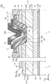
- FIG. 1 is a cross-sectional view of a nitride semiconductor device according to Embodiment 1.
- FIG. FIG. 2 is a plan view of the nitride semiconductor device according to Embodiment 1.
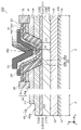
- FIG. 3 is a cross-sectional view of a nitride semiconductor device according to Embodiment 2.
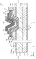
- FIG. 4 is a cross-sectional view of a nitride semiconductor device according to Embodiment 3.
- FIG. FIG. 5 is a cross-sectional view of a nitride semiconductor device according to a fourth embodiment.
- FIG. 6 is a cross-sectional view of a nitride semiconductor device according to a modification of the fourth embodiment.
- FIG. 1 is a cross-sectional view of a nitride semiconductor device according to Embodiment 1.
- FIG. FIG. 2 is a plan view of the nitride semiconductor device according to Embodiment 1.
- FIG. 3 is a cross-sectional view of
- FIG. 7 is a cross-sectional view of a nitride semiconductor device according to Embodiment 5.
- FIG. 8 is a cross-sectional view of a nitride semiconductor device according to Modification 1 of Embodiment 5.
- FIG. 9 is a cross-sectional view of a nitride semiconductor device according to Modification 2 of Embodiment 5.
- FIG. 10 is a plan view of a nitride semiconductor device according to Modification 2 of Embodiment 5.
- the isolation trench disclosed in Patent Document 2 is formed by dry etching. In the vicinity of the isolation trench, deterioration of film quality is likely to occur due to damage during dry etching.
- the present disclosure provides a nitride semiconductor device with improved off characteristics. Specifically, the present invention provides a nitride semiconductor device capable of reducing leakage current in an off state and suppressing a decrease in breakdown voltage.
- a nitride semiconductor device includes a substrate, a first semiconductor layer of a first conductivity type disposed above the substrate, and a first semiconductor layer disposed above the first semiconductor layer. a second semiconductor layer of conductivity type 2; a third semiconductor layer disposed above the second semiconductor layer; a first opening reaching one semiconductor layer, a part of which is arranged along the inner surface of the first opening, and another part of which is arranged above the third semiconductor layer, a semiconductor multilayer film having a channel region of a first conductivity type; a fourth semiconductor layer of the second conductivity type disposed along the upper surface of the semiconductor multilayer film; a gate electrode arranged; a source electrode arranged apart from the gate electrode; a drain electrode arranged on the lower surface side of the substrate; and a trench penetrating through the semiconductor layer to reach the first semiconductor layer, wherein the distance between the bottom of the first opening and the substrate is shorter than the distance between the bottom of the trench and the substrate.
- a pn junction exists between the semiconductor multilayer film and the fourth semiconductor layer in the first opening. Since the fourth semiconductor layer can be formed continuously from the semiconductor multilayer film, this pn junction provides a higher quality pn junction with a higher electric field strength than the pn junction near the groove where etching damage occurs. .
- the bottom of the first opening is closer to the substrate than the bottom of the groove. It is easy to concentrate on one opening. Therefore, electric field concentration can be received at the high-quality pn junction, and electric field concentration on the pn junction near the groove can be alleviated. This can improve the off characteristics of the nitride semiconductor device. Specifically, the leak current in the vicinity of the groove can be reduced, and the decrease in breakdown voltage can be suppressed.
- the distance between the bottom of the fourth semiconductor layer and the substrate in the first opening may be shorter than the distance between the bottom of the groove and the substrate.
- the pn junction in the first opening is closer to the substrate than the pn junction in the vicinity of the groove, so that the pn junction in the first opening can receive electric field concentration. Therefore, the off characteristics of the nitride semiconductor device can be improved.
- the second semiconductor layer is provided apart from the gate electrode and penetrates through the semiconductor multilayer film and the third semiconductor layer. and the source electrode may be provided along an inner surface of the second opening.
- the channel region and the source electrode included in the semiconductor multilayer film are in direct contact with each other, so that the contact resistance between the channel region and the source electrode can be reduced.
- the potential of the second semiconductor layer can be fixed to the potential of the source electrode. Since current collapse is suppressed by fixing the potential of the second semiconductor layer, the dynamic characteristics of the nitride semiconductor device can be improved.
- the first semiconductor layer is composed of a plurality of layers having different impurity concentrations, and the bottom of the first opening is the n-th layer (n is 2 or more) from the top among the plurality of layers. natural number) of layers.
- each layer can have a suitable function by multilayering the first semiconductor layer. For example, it is possible to improve the off-characteristics while suppressing an increase in the on-resistance of the nitride semiconductor device.
- the bottom of the groove may be located in a layer above the n-th layer.
- the plurality of layers may be composed of two layers.
- the impurity concentration of the n-th layer where the bottom of the first opening is located can be made higher than the impurity concentration of the layer where the bottom of the trench is located.
- the impurity concentration of the n-th layer where the bottom of the first opening is located can be made higher than the impurity concentration of the layer where the bottom of the trench is located.
- the bottom of the first opening is located in the n-th layer with high impurity concentration and low resistance, the layer with low impurity concentration and high resistance is located on the path of the drain current. do not do. Therefore, an increase in on-resistance can be suppressed.
- a layer having a low impurity concentration and a high resistance is not positioned. can be subjected to electric field concentrations at Therefore, deterioration of the OFF characteristics of the nitride semiconductor device is suppressed.
- the plurality of layers may be composed of three layers.
- the n-th layer may be a layer having the highest impurity concentration among the plurality of layers.
- the diffusion of the drain current in the lateral direction can be promoted through the layer with the highest impurity concentration, so the on-resistance reduction effect can be maximized.
- the uppermost layer among the plurality of layers may be a layer having a lower impurity concentration of the first conductivity type than the n-th layer.
- the bottom of the groove may be located in the n-th layer.
- reverse conduction deterioration deterioration of the off-characteristics of the nitride semiconductor device. According to the nitride semiconductor device according to this aspect, reverse conduction deterioration can be suppressed.
- the bottom of the groove may be located on the uppermost layer.
- the top layer may contain C or Fe.
- the nitride semiconductor device further includes an insulating film provided along the inner surface of the trench, and a field provided above the insulating film so as to protrude into the trench. and a plate.
- the field plate may be electrically connected to the source electrode.
- the effect of dispersing the electric field concentrated on the terminal end to the field plate can be maximized, so that the effect of alleviating the electric field concentration on the pn junction near the groove can be further enhanced.
- the smaller angle between the sidewalls of the groove and the plane parallel to the main surface of the substrate may be less than 90°.
- the groove is provided in a ring shape that collectively surrounds the first opening, the semiconductor multilayer film, the fourth semiconductor layer, the gate electrode and the source electrode in a plan view
- the semiconductor layer 1 may include a high-resistance region provided in a ring shape along the bottom of the trench and into which an impurity is introduced.
- an interface level is formed at the interface between the insulating film and the first semiconductor layer, which may result in the formation of a leakage current path.
- a leak current flows through this path, degrading the OFF characteristics.
- the leakage current can be suppressed by the high resistance region, so that the OFF characteristics can be improved.
- the impurity contained in the high resistance region may be Mg, B or Fe.
- the high resistance region may include an end surface of the nitride semiconductor device.
- the end face of the nitride semiconductor device is formed by, for example, dicing. Damage caused by dicing may create a leakage current path.
- the leakage current can be suppressed by the high resistance region, so that the OFF characteristics can be improved.
- each figure is a schematic diagram and is not necessarily strictly illustrated. Therefore, for example, scales and the like do not necessarily match in each drawing. Moreover, in each figure, substantially the same configurations are denoted by the same reference numerals, and overlapping descriptions are omitted or simplified.
- the x-axis, y-axis and z-axis indicate three axes of a three-dimensional orthogonal coordinate system.
- the x-axis and the y-axis are directions parallel to the first side of the rectangle and the second side orthogonal to the first side, respectively, when the substrate has a rectangular shape in plan view.
- the z-axis is the thickness direction of the substrate.
- the "thickness direction" of the substrate refers to the direction perpendicular to the main surface of the substrate.
- the thickness direction is the same as the stacking direction of the semiconductor layers, and is also referred to as the “longitudinal direction”.
- a direction parallel to the main surface of the substrate may be referred to as a "lateral direction”.
- the side of the substrate on which the gate electrode and the source electrode are provided (the positive side of the z-axis) is regarded as the “upper side” or the “upper side”
- the side of the substrate on which the drain electrode is provided (the negative side of the z-axis) is regarded as the “upper side”. side) as "lower” or "lower”.
- the terms “upper” and “lower” do not refer to the upward direction (vertically upward) and the downward direction (vertically downward) in absolute spatial recognition, but are based on the stacking order in the stacking structure. It is used as a term defined by a relative positional relationship. Also, the terms “above” and “below” are used only when two components are spaced apart from each other and there is another component between them, as well as when two components are spaced apart from each other. It also applies when two components are in contact with each other and are placed in close contact with each other.
- planar view means when viewed from a direction perpendicular to the main surface of the substrate of the nitride semiconductor device, that is, when the main surface of the substrate is viewed from the front. .
- ordinal numbers such as “first” and “second” do not mean the number or order of components, unless otherwise specified, to avoid confusion between components of the same kind and to distinguish them. It is used for the purpose of
- AlGaN represents a ternary mixed crystal Al x Ga 1-x N (0 ⁇ x ⁇ 1).
- multi-element mixed crystals are abbreviated by the arrangement of their constituent element symbols, eg, AlInN, GaInN, and the like.
- AlxGa1 - xyInyN (0 ⁇ x ⁇ 1, 0 ⁇ y ⁇ 1, and 0 ⁇ x+y ⁇ 1), which is an example of a nitride semiconductor, is abbreviated as AlGaInN.
- FIG. 1 is a cross-sectional view of a nitride semiconductor device 1 according to this embodiment.
- FIG. 2 is a plan view of nitride semiconductor device 1 according to the present embodiment.
- FIG. 1 shows a cross section taken along line II of FIG.
- the transistor portion 2 and the terminal portion 3 are schematically shown separately.
- the nitride semiconductor device 1 includes a transistor portion 2 and a termination portion 3.
- the nitride semiconductor device 1 includes a substrate 10, a drift layer 12, a first underlayer 14, a second underlayer 16, a gate opening 18, a semiconductor multilayer film 20, a threshold value It comprises an adjustment layer 24 , a source opening 26 , a source electrode 28 , a gate electrode 30 and a drain electrode 32 .
- the semiconductor multilayer film 20 is a laminate of an electron transit layer 21 and an electron supply layer 22, and includes a two-dimensional electron gas (2DEG) 23 as a channel region.
- Nitride semiconductor device 1 also includes groove portion 40 provided in terminal portion 3 .
- the transistor section 2 is a region containing FETs, and is a region containing the center of the nitride semiconductor device 1 as shown in FIG. Specifically, the transistor section 2 is a region in which the second base layer 16, the gate opening 18, the semiconductor multilayer film 20, the threshold adjustment layer 24, the gate electrode 30 and the source electrode 28 are arranged in plan view. .
- each component arranged in the transistor section 2 is omitted.
- a plurality of source electrodes 28 elongated in one direction in plan view are arranged in stripes, and gate electrodes 30, threshold adjustment layers 24, and gate openings 18 are arranged between adjacent source electrodes 28.
- a plurality of source electrodes 28 having a hexagonal shape in plan view may be arranged so as to be planarly filled with a gap therebetween.
- the terminal portion 3 is a region other than the transistor portion 2 and is provided in a ring shape surrounding the transistor portion 2 .
- the second underlying layer 16 , the gate opening 18 , the semiconductor multilayer film 20 , the threshold adjustment layer 24 , the gate electrode 30 and the source electrode 28 are not arranged in the terminal portion 3 .
- the nitride semiconductor device 1 is a device having a laminated structure of semiconductor layers mainly composed of nitride semiconductors such as GaN and AlGaN. Specifically, nitride semiconductor device 1 has a heterostructure of an AlGaN film and a GaN film.
- a high-concentration two-dimensional electron gas 23 is generated at the heterointerface by spontaneous polarization or piezoelectric polarization on the (0001) plane. Therefore, even in an undoped state, a sheet carrier concentration of 1 ⁇ 10 13 cm ⁇ 2 or more can be obtained at the interface.
- the nitride semiconductor device 1 is a field effect transistor (FET) using a two-dimensional electron gas 23 generated at the AlGaN/GaN heterointerface as a channel.
- FET field effect transistor
- the nitride semiconductor device 1 is a so-called vertical FET.
- the nitride semiconductor device 1 is a normally-off FET.
- the source electrode 28 is grounded (that is, the potential is 0V), and the drain electrode 32 is given a positive potential.
- the potential applied to the drain electrode 32 is, for example, 100 V or more and 1200 V or less, but is not limited thereto.
- gate electrode 30 is applied with 0V or a negative potential (eg, -5V).
- gate electrode 30 is applied with a positive potential (for example, +5 V).
- Nitride semiconductor device 1 may be a normally-on FET.
- the substrate 10 is a substrate made of a nitride semiconductor, and has a first principal surface 10a and a second principal surface 10b facing each other, as shown in FIG.
- the first main surface 10a is the main surface (upper surface) on which the drift layer 12 is formed.
- the first main surface 10a substantially coincides with the c-plane.
- the second main surface 10b is the main surface (lower surface) on which the drain electrode 32 is formed.
- the planar view shape of the substrate 10 is, for example, a rectangle, but is not limited to this.
- the substrate 10 is, for example, a substrate made of n + -type GaN having a thickness of 300 ⁇ m and a carrier concentration of 1 ⁇ 10 18 cm ⁇ 3 .
- n-type and p-type indicate conductivity types of semiconductors.
- the n + type represents a state in which an n-type dopant is added to a semiconductor at a high concentration, ie, so-called heavy doping.
- n ⁇ type represents a state in which an n-type dopant is added to a semiconductor at a low concentration, ie, so-called light doping.
- p + type and p ⁇ type The same is true for p + type and p ⁇ type.
- N-type, n + -type and n - -type are examples of the first conductivity type.
- P-type, p + -type and p - -type are examples of the second conductivity type.
- the second conductivity type is a conductivity type opposite in polarity to the first conductivity type.
- the substrate 10 does not have to be a nitride semiconductor substrate.
- the substrate 10 may be a silicon (Si) substrate, a silicon carbide (SiC) substrate, a zinc oxide (ZnO) substrate, or the like.
- Drift layer 12 is an example of a first conductivity type first nitride semiconductor layer disposed above substrate 10 .
- the drift layer 12 is, for example, a film made of n ⁇ -type GaN with a thickness of 8 ⁇ m.
- the donor concentration of the drift layer 12 is, for example, in the range of 1 ⁇ 10 15 cm ⁇ 3 or more and 1 ⁇ 10 17 cm ⁇ 3 or less, and is 1 ⁇ 10 16 cm ⁇ 3 as an example.
- the carbon concentration (C concentration) of the drift layer 12 is in the range of 1 ⁇ 10 15 cm ⁇ 3 to 2 ⁇ 10 17 cm ⁇ 3 .
- the drift layer 12 is provided in contact with the first main surface 10a of the substrate 10, for example.
- the drift layer 12 is formed on the first main surface 10a of the substrate 10 by, for example, crystal growth such as metal-organic vapor phase epitaxy (MOVPE).
- MOVPE metal-organic vapor phase epitaxy
- the first underlayer 14 is an example of a second conductivity type second nitride semiconductor layer disposed above the drift layer 12 .
- the first underlayer 14 is, for example, a film made of p-type GaN having a thickness of 400 nm and a carrier concentration of 1 ⁇ 10 17 cm ⁇ 3 .
- the first underlayer 14 is provided in contact with the upper surface of the drift layer 12 .
- the first underlayer 14 is formed on the drift layer 12 by, for example, crystal growth such as the MOVPE method. Note that the first underlayer 14 may be formed by injecting magnesium (Mg) into a deposited undoped GaN film. Undoping will be explained later.
- Mg magnesium
- the first underlayer 14 suppresses leak current between the source electrode 28 and the drain electrode 32 .
- the potential of the drain electrode 32 becomes higher than that of the source electrode 28.
- a depletion layer extends in the drift layer 12 .
- the potential of the drain electrode 32 is higher than that of the source electrode 28 both in the OFF state and the ON state. Therefore, the nitride semiconductor device 1 can have a high withstand voltage.
- the first underlying layer 14 is in contact with the source electrode 28, as shown in FIG. Therefore, the first underlying layer 14 is fixed at the same potential as the source electrode 28 .
- the second underlying layer 16 is an example of a third nitride semiconductor layer provided above the first underlying layer 14 .
- the second underlayer 16 is a high resistance layer having a higher resistance than the first underlayer 14 .
- the second underlying layer 16 is made of an insulating or semi-insulating nitride semiconductor.
- the second underlayer 16 is, for example, a film made of undoped GaN with a thickness of 200 nm.
- the second underlayer 16 is provided in contact with the first underlayer 14 .
- the second underlayer 16 is formed on the first underlayer 14 by, for example, crystal growth such as the MOVPE method.
- the second underlayer 16 is doped with carbon (C). Specifically, the carbon concentration of the second underlayer 16 is higher than the carbon concentration of the first underlayer 14 .
- the second underlayer 16 may contain silicon (Si) or oxygen (O) mixed during film formation.
- the carbon concentration of the second underlayer 16 is higher than the silicon concentration (Si concentration) or the oxygen concentration (O concentration).
- the carbon concentration of the second underlayer 16 is, for example, 3 ⁇ 10 17 cm ⁇ 3 or more, but may be 1 ⁇ 10 18 cm ⁇ 3 or more.
- the silicon concentration or oxygen concentration of the second underlayer 16 is, for example, 5 ⁇ 10 16 cm ⁇ 3 or less, but may be 2 ⁇ 10 16 cm ⁇ 3 or less.
- the second underlayer 16 may be formed by ion implantation of magnesium (Mg), iron (Fe), boron (B), or the like, other than carbon.
- Mg magnesium
- Fe iron
- B boron
- Other ion species may be used as long as they are ion species capable of realizing high resistance of GaN.
- the nitride semiconductor device 1 does not include the second underlying layer 16, the electron transit layer 21 and the p-type first underlying layer 14 are interposed between the source electrode 28 and the drain electrode 32.
- the formation of a parasitic npn structure can be suppressed by providing the high-resistance second base layer 16 , and malfunction of the nitride semiconductor device 1 can be suppressed.
- a layer for suppressing diffusion of p-type impurities such as Mg from the first underlayer 14 may be provided on the upper surface of the second underlayer 16 .
- an AlGaN layer having a thickness of 20 nm may be provided on the second underlayer 16 .
- the gate opening 18 is an example of a first opening that penetrates the second underlying layer 16 and the first underlying layer 14 and reaches the drift layer 12 .
- the gate opening 18 penetrates both the second underlayer 16 and the first underlayer 14 .
- a bottom portion 18 a of the gate opening 18 is part of the upper surface of the drift layer 12 .
- the bottom portion 18a is located below the lower surface of the first underlayer 14.
- the lower surface of the first underlayer 14 corresponds to the interface between the first underlayer 14 and the drift layer 12 .
- the bottom portion 18a is parallel to the first major surface 10a of the substrate 10, for example.
- the gate opening 18 is formed such that the opening area increases as the distance from the substrate 10 increases. Specifically, the sidewall 18b of the gate opening 18 is obliquely inclined. As shown in FIG. 1, the cross-sectional shape of the gate opening 18 is an inverted trapezoid, more specifically, an inverted isosceles trapezoid.
- the inclination angle of the side wall 18b with respect to the bottom portion 18a is, for example, in the range of 30° or more and 45° or less.
- the smaller the tilt angle the closer the side wall 18b is to the c-plane, so the film quality of the electron transit layer 21 formed along the side wall 18b by crystal regrowth can be improved.
- the larger the tilt angle the more the gate opening 18 is prevented from becoming too large, and the size reduction of the nitride semiconductor device 1 is realized.
- the gate opening 18 is formed on the first main surface 10a of the substrate 10 by successively forming the drift layer 12, the first underlayer 14, and the second underlayer 16 in this order. It is formed by removing a portion of each of the second underlayer 16 and the first underlayer 14 so as to expose the drift layer 12 roughly. At this time, by removing the surface layer portion of the drift layer 12 by a predetermined thickness, the bottom portion 18 a of the gate opening portion 18 is formed below the lower surface of the first underlying layer 14 .
- the removal of the second underlayer 16 and the first underlayer 14 is performed by resist coating and patterning, and dry etching. Specifically, after patterning the resist, baking is performed so that the edges of the resist are slanted. By performing dry etching after that, the gate opening 18 is formed so that the side wall 18b is slanted so that the shape of the resist is transferred.
- a part of the semiconductor multilayer film 20 is arranged along the inner surface of the gate opening 18 and another part is arranged above the second underlying layer 16 .
- the semiconductor multilayer film 20 is a laminated film of an electron transit layer 21 and an electron supply layer 22 .
- the electron transit layer 21 is an example of a first regrowth layer provided along the inner surface of the gate opening 18 . Specifically, part of the electron transit layer 21 is provided along the bottom 18 a and sidewalls 18 b of the gate opening 18 , and the other part of the electron transit layer 21 is provided on the upper surface of the second underlying layer 16 . is provided.
- the electron transit layer 21 is, for example, a film made of undoped GaN with a thickness of 150 nm.
- the electron transit layer 21 may be made n-type by Si doping instead of undoping.
- the electron transit layer 21 is in contact with the drift layer 12 at the bottom 18a and sidewalls 18b of the gate opening 18.
- the electron transit layer 21 is in contact with the end face of each of the first underlying layer 14 and the second underlying layer 16 at the sidewall 18 b of the gate opening 18 . Furthermore, the electron transit layer 21 is in contact with the upper surface of the second underlayer 16 .
- the electron transit layer 21 is formed by crystal re-growth after forming the gate opening 18 .
- the electron transit layer 21 has a channel region. Specifically, a two-dimensional electron gas 23 is generated near the interface between the electron transit layer 21 and the electron supply layer 22 . Two-dimensional electron gas 23 functions as a channel of electron transit layer 21 . In FIG. 1, the two-dimensional electron gas 23 is schematically illustrated by broken lines. The two-dimensional electron gas 23 bends along the interface between the electron transit layer 21 and the electron supply layer 22 , that is, along the inner surface of the gate opening 18 .
- an AlN film having a thickness of about 1 nm may be provided as a second regrowth layer between the electron transit layer 21 and the electron supply layer 22 .
- the AlN film can suppress alloy scattering and improve channel mobility.
- the electron supply layer 22 is an example of a third regrowth layer provided along the inner surface of the gate opening 18 .
- the electron transit layer 21 and the electron supply layer 22 are provided in this order from the substrate 10 side.
- the electron supply layer 22 is formed in a shape along the upper surface of the electron transit layer 21 with a substantially uniform thickness.
- the electron supply layer 22 is, for example, a film made of undoped AlGaN with a thickness of 50 nm.
- the electron supply layer 22 is formed by crystal regrowth following the step of forming the electron transit layer 21 .
- the electron supply layer 22 forms an AlGaN/GaN heterointerface with the electron transit layer 21 . As a result, a two-dimensional electron gas 23 is generated within the electron transit layer 21 .
- the electron supply layer 22 supplies electrons to the channel region (that is, the two-dimensional electron gas 23) formed in the electron transit layer 21.
- the threshold adjustment layer 24 is an example of a second conductivity type fourth nitride semiconductor layer arranged along the upper surface of the semiconductor multilayer film 20 . Specifically, the threshold adjustment layer 24 is provided between the gate electrode 30 and the electron supply layer 22 . The threshold value adjustment layer 24 is formed in a shape along the upper surface of the electron supply layer 22 with a substantially uniform thickness.
- the threshold adjustment layer 24 is, for example, a nitride semiconductor layer made of p-type GaN or AlGaN having a thickness of 100 nm and a carrier concentration of 1 ⁇ 10 17 cm ⁇ 3 .
- the threshold adjustment layer 24 is formed by regrowth by the MOVPE method subsequent to the step of forming the electron supply layer 22 and patterning.
- the threshold adjustment layer 24 raises the potential of the conduction band edge of the channel portion. Therefore, the threshold voltage of nitride semiconductor device 1 can be increased. Therefore, the nitride semiconductor device 1 can be realized as a normally-off FET. That is, when a potential of 0 V is applied to gate electrode 30, nitride semiconductor device 1 can be turned off.
- the source opening 26 is an example of a second opening that penetrates the semiconductor multilayer film 20 and the second underlying layer 16 to reach the first underlying layer 14 at a position away from the gate opening 18 .
- the source opening 26 is arranged at a position distant from the gate electrode 30 in plan view.
- a bottom portion 26 a of the source opening 26 is part of the upper surface of the first underlayer 14 . As shown in FIG. 1 , the bottom portion 26 a is located below the bottom surface of the second underlayer 16 . The bottom surface of the second underlayer 16 corresponds to the interface between the second underlayer 16 and the first underlayer 14 . The bottom portion 26a is parallel to the first major surface 10a of the substrate 10, for example.
- the source opening 26 is formed so that the opening area is constant regardless of the distance from the substrate 10 .
- sidewalls 26b of source opening 26 are perpendicular to bottom 26a. That is, the cross-sectional shape of the source opening 26 is rectangular.
- the source opening 26 may be formed so that the opening area increases as the distance from the substrate 10 increases.
- the sidewall 26b of the source opening 26 may be obliquely slanted.
- the cross-sectional shape of the source opening 26 may be an inverted trapezoid, more specifically, an inverted isosceles trapezoid.
- the inclination angle of the side wall 26b with respect to the bottom portion 26a may be, for example, in the range of 30° or more and 60° or less.
- sidewalls 26 b of source opening 26 may have a greater slope angle than sidewalls 18 b of gate opening 18 .
- the contact area between the source electrode 28 and the electron transit layer 21 (two-dimensional electron gas 23) is increased, thereby facilitating ohmic connection.
- the two-dimensional electron gas 23 is exposed on the sidewall 26b of the source opening 26 and connected to the source electrode 28 at the exposed portion.
- the source opening 26 may be formed, for example, following the step of forming the threshold adjusting layer 24 (i.e., the crystal regrowth step), such that the first underlying layer 14 is exposed in a different region than the gate opening 18 . It is formed by etching the adjustment layer 24 , the electron supply layer 22 , the electron transit layer 21 and the second underlayer 16 . At this time, the surface layer portion of the first underlying layer 14 is also removed, so that the bottom portion 26 a of the source opening 26 is formed below the lower surface of the second underlying layer 16 .
- the source opening 26 is formed into a predetermined shape by, for example, photolithographic patterning and dry etching.
- the source electrode 28 is arranged apart from the gate electrode 30 .
- the source electrode 28 is provided along the inner surface of the source opening 26 .
- the source electrode 28 is connected to each of the electron supply layer 22 , the electron transit layer 21 and the first underlying layer 14 .
- the source electrode 28 is ohmic-connected to each of the electron transit layer 21 and the electron supply layer 22 .
- Source electrode 28 is in direct contact with two-dimensional electron gas 23 at sidewall 26b. Thereby, the contact resistance between the source electrode 28 and the two-dimensional electron gas 23 (channel) can be reduced.
- the source electrode 28 is formed using a conductive material such as metal.
- a material such as Ti/Al that can be ohmic-connected to the n-type GaN layer by heat treatment can be used.
- the source electrode 28 is formed, for example, by patterning a conductive film formed by sputtering or vapor deposition.
- the gate electrode 30 is arranged above the threshold adjustment layer 24 . Specifically, the gate electrode 30 is provided in contact with the upper surface of the threshold adjustment layer 24 so as to cover the gate opening 18 .
- the gate electrode 30 is formed, for example, in a shape along the upper surface of the threshold value adjustment layer 24 with a substantially uniform film thickness. Alternatively, the gate electrode 30 may be formed so as to fill the concave portion of the upper surface of the threshold adjustment layer 24 .
- the gate electrode 30 is formed using a conductive material such as metal.
- the gate electrode 30 is formed using palladium (Pd).
- a material that is Schottky-connected to the p-type GaN layer can be used, such as a nickel (Ni)-based material, tungsten silicide (WSi), gold (Au), or the like.
- the gate electrode 30 is formed by patterning a conductive film formed by, for example, sputtering or vapor deposition after the threshold adjustment layer 24 is formed, the source opening 26 is formed, or the source electrode 28 is formed. be.
- the drain electrode 32 is provided on the lower surface side of the substrate 10 , that is, on the side opposite to the drift layer 12 . Specifically, the drain electrode 32 is provided in contact with the second main surface 10b of the substrate 10 .
- the drain electrode 32 is formed using a conductive material such as metal.
- a material such as Ti/Al which is ohmically connected to the n-type GaN layer can be used.
- the drain electrode 32 is formed, for example, by patterning a conductive film deposited by sputtering or vapor deposition.
- the second base layer 16, the semiconductor multilayer film 20, and the threshold adjustment layer 24 are not provided in the terminal portion 3.
- the second underlying layer 16, the semiconductor multilayer film 20, and the threshold adjustment layer 24 are removed at the termination portion 3 at the same time as the source opening portion 26 is formed.
- the top surface of the first underlying layer 14 is positioned at the same height as the bottom portion 26 a of the source opening 26 .
- “same height” means that the distances from the first main surface 10a of the substrate 10 are the same.
- a groove portion 40 is provided in the terminal end portion 3 .
- the groove portion 40 is an isolation trench for partitioning and isolating the transistor portion 2 .
- the groove portion 40 penetrates the first underlayer 14 and reaches the drift layer 12 .
- the groove portion 40 has a bottom portion 40a and side walls 40b.
- the groove portion 40 is a stepped portion having sidewalls 40b only on the transistor portion 2 side. That is, the bottom portion 40a of the groove portion 40 is connected to the end face of the nitride semiconductor device 1. As shown in FIG.
- the groove portion 40 is provided in a ring shape surrounding the transistor portion 2, as shown in FIG.
- a bottom portion 40 a of the groove portion 40 is part of the upper surface of the drift layer 12 . As shown in FIG. 1, the bottom portion 40a is located below the lower surface of the first underlayer 14. As shown in FIG. The bottom portion 40a is parallel to the first main surface 10a of the substrate 10, for example.
- the groove part 40 is formed so that the opening area is constant regardless of the distance from the substrate 10 .
- sidewalls 40b of groove 40 are perpendicular to bottom 40a. That is, the cross-sectional shape of the groove portion 40 is rectangular.
- the trench 40 is formed, for example, by performing dry etching with a different etching mask following the dry etching process for forming the source opening 26 .
- the trench 40 may be formed by dry etching.
- the distance between the bottom 18a of the gate opening 18 and the first main surface 10a of the substrate 10 is D1.
- the distance between the bottom portion 24a of the threshold adjustment layer 24 and the first main surface 10a of the substrate 10 is defined as D2.
- the distance between the bottom portion 40a of the groove portion 40 and the first main surface 10a of the substrate 10 is defined as D3.
- the distance D1 is shorter than the distance D3.
- the distance D2 is shorter than the distance D3. That is, D1 ⁇ D2 ⁇ D3 is established.
- the difference between the distance D1 and the distance D3 is 0.05 ⁇ m or more and 1 ⁇ m or less. More preferably, it is 0.1 ⁇ m or more and 0.5 ⁇ m or less.
- the off characteristics of the nitride semiconductor device 1 can be improved. Specifically, it is as follows.
- the transistor section 2 When the transistor section 2 is in the off state, a high voltage is applied between the drain electrode 32 and the source electrode 28 such that the potential on the drain electrode 32 side is higher than that on the source electrode 28 side. Therefore, in the off state, a high electric field is generated in the longitudinal direction of nitride semiconductor device 1 .
- both the distances D1 and D2 are shorter than the distance D3, the electric field tends to concentrate on the gate opening 18 of the transistor section 2 rather than on the terminal section 3 .
- a concentrated electric field can be received by the pn junction between the threshold adjustment layer 24 and the semiconductor multilayer film 20 .
- This pn junction has higher quality and higher electric field strength than the pn junction between the first underlying layer 14 and the drift layer 12 in the vicinity of the groove 40 where etching damage occurs. Since the pn junction having a high electric field intensity can receive the electric field concentration, the electric field concentration on the pn junction near the trench 40 can be alleviated. Thereby, the off characteristics of the nitride semiconductor device 1 can be improved. Specifically, the leak current in the vicinity of the groove portion 40 can be reduced, and the decrease in breakdown voltage can be suppressed. As the difference between the distance D1 and the distance D3 increases, the electric field concentration in the vicinity of the groove 40 can be alleviated.
- the second embodiment differs from the first embodiment in that the drift layer has a two-layer structure.
- the following description focuses on the differences from the first embodiment, and omits or simplifies the description of the common points.
- FIG. 3 is a cross-sectional view of nitride semiconductor device 101 according to the present embodiment. As shown in FIG. 3 , nitride semiconductor device 101 includes drift layer 112 instead of drift layer 12 compared to nitride semiconductor device 1 according to the first embodiment.
- the drift layer 112 is composed of a plurality of layers with different impurity concentrations.
- the plurality of layers is composed of two layers.
- the drift layer 112 has a high concentration layer 112a and a low concentration layer 112b.
- the high-concentration layer 112a and the low-concentration layer 112b are continuously formed on the substrate 10 by, for example, crystal growth such as the MOVPE method.
- the high-concentration layer 112a is an example of the n-th layer from the top among the plurality of layers. n is a natural number of 2 or more. In this embodiment, n is two. High-concentration layer 112 a is provided in contact with first main surface 10 a of substrate 10 . The bottom portion 18a of the gate opening portion 18 is located in the high-concentration layer 112a.
- the high-concentration layer 112a is, for example, a film made of n + -type GaN with a thickness of 7 ⁇ m.
- the impurity concentration (donor concentration) of the high-concentration layer 112a is, for example, in the range of 3 ⁇ 10 15 cm ⁇ 3 or more and 5 ⁇ 10 16 cm ⁇ 3 or less, and is 1.5 ⁇ 10 16 cm ⁇ 3 as an example. .
- the low-concentration layer 112b is an example of a layer located above the n-th layer.
- low-concentration layer 112b is the uppermost layer in drift layer 112, and is provided between high-concentration layer 112a and first underlayer 14 in contact with each other.
- the low-concentration layer 112b has a lower impurity concentration than the high-concentration layer 112a.
- a bottom portion 40a of the groove portion 40 is located in the low-concentration layer 112b.
- the low-concentration layer 112b is, for example, a film made of n ⁇ -type GaN with a thickness of 1 ⁇ m.
- the impurity concentration (donor concentration) of the low-concentration layer 112b is, for example, in the range of 1 ⁇ 10 15 cm ⁇ 3 or more and 3 ⁇ 10 16 cm ⁇ 3 or less, and is 9 ⁇ 10 15 cm ⁇ 3 as an example.
- the OFF state is achieved.
- a high voltage is applied to the drain electrode 32 at , extension of the depletion layer into the drift layer 112 is promoted. Thereby, the breakdown voltage of the nitride semiconductor device 101 can be increased.
- the distance D3 is shorter than either of the distances D1 and D2
- the OFF characteristics of the nitride semiconductor device 101 can be improved as in the first embodiment. .
- the bottom 18a of the gate opening 18 is located within the high-concentration layer 112a.
- the drain current in the ON state flows from the drain electrode 32 to the source electrode 28 through the substrate 10 , the high-concentration layer 112 a and the two-dimensional electron gas 23 . Since the low-concentration layer 112b with high resistance does not exist on the path of the drain current, the on-resistance can be reduced.
- the third embodiment differs from the second embodiment in the number of drift layers.
- the following description focuses on the differences from the second embodiment, and omits or simplifies the description of the common points.
- FIG. 4 is a cross-sectional view of a nitride semiconductor device 201 according to this embodiment. As shown in FIG. 4 , nitride semiconductor device 201 includes drift layer 212 instead of drift layer 112 compared to nitride semiconductor device 101 according to the second embodiment.
- the drift layer 212 is composed of a plurality of layers with different impurity concentrations.
- the plurality of layers is composed of three layers.
- the drift layer 212 has a high-concentration layer 112a, an ultra-high-concentration layer 212c, and a low-concentration layer 112b.
- High-concentration layer 112a and low-concentration layer 112b are the same as in the second embodiment.
- the high-concentration layer 112a, the ultra-high-concentration layer 212c, and the low-concentration layer 112b are continuously formed on the substrate 10 by, for example, crystal growth such as the MOVPE method.
- the ultra-high concentration layer 212c is an example of the n-th layer among the multiple layers. That is, in the present embodiment, the high-concentration layer 112a is a layer located below the n-th layer. n is two. The super high concentration layer 212c is provided between the high concentration layer 112a and the low concentration layer 112b in contact with each other. The ultra-high concentration layer 212 c is the layer with the highest impurity concentration among the plurality of layers forming the drift layer 212 .
- the ultra-high concentration layer 212c is, for example, a film made of n + -type GaN with a thickness of 0.2 ⁇ m.
- the impurity concentration (donor concentration) of the ultra-high concentration layer 212c is, for example, in the range of 1 ⁇ 10 16 cm ⁇ 3 or more and 1 ⁇ 10 18 cm ⁇ 3 or less, and is 1 ⁇ 10 17 cm ⁇ 3 as an example.
- the bottom 18a of the gate opening 18 is located in the ultra-high concentration layer 212c. Since the ultra-high concentration layer 212c has a high impurity concentration and a low resistance, the drain current passing through the bottom portion 18a of the gate opening 18 diffuses laterally in the ultra-high concentration layer 212c. That is, the lateral diffusion of the drain current in the drift layer 212 is promoted, so that the on-resistance of the nitride semiconductor device 201 can be reduced.
- the low-concentration layer 112b and the first underlying layer 14 are connected, so extension of the depletion layer into the drift layer 212 is promoted. Therefore, the breakdown voltage of nitride semiconductor device 201 can be increased. Further, the nitride semiconductor device 201 can improve the off characteristics as in the first embodiment.
- the impurity concentration of the uppermost layer of the drift layer is different from that in the second embodiment.
- the following description focuses on the differences from the second embodiment, and omits or simplifies the description of the common points.
- FIG. 5 is a cross-sectional view of a nitride semiconductor device 301 according to this embodiment. As shown in FIG. 5 , nitride semiconductor device 301 includes drift layer 312 instead of drift layer 112 compared to nitride semiconductor device 101 according to the second embodiment.
- the drift layer 312 is composed of a plurality of layers with different impurity concentrations.
- the plurality of layers is composed of two layers.
- the drift layer 312 has a low resistance layer 312a and a high resistance layer 312b.
- Low-resistance layer 312a is substantially the same as drift layer 12 according to the first embodiment.
- the low resistance layer 312a and the high resistance layer 312b are continuously formed on the substrate 10 by crystal growth such as MOVPE, for example.
- the high-resistance layer 312 b is the uppermost layer among the multiple layers forming the drift layer 312 .
- the high resistance layer 312b is arranged between the low resistance layer 312a and the first underlying layer 14 in contact with each other.
- the high-resistance layer 312b is a layer having a lower impurity concentration of the first conductivity type than the low-resistance layer 312a.
- the high-resistance layer 312b is, for example, a layer having higher resistance than both the low-resistance layer 312a and the first underlying layer 14 .
- the high resistance layer 312b is made of, for example, an insulating or semi-insulating nitride semiconductor.
- the impurity concentration (donor concentration) of the high resistance layer 312b is, for example, 1 ⁇ 10 16 cm ⁇ 3 or less.
- the high resistance layer 312b is, for example, a film made of undoped GaN with a thickness of 200 nm.
- the high resistance layer 312b contains carbon (C) or iron (Fe).
- the carbon concentration or iron concentration of the high resistance layer 312b is, for example, in the range of 2 ⁇ 10 16 cm ⁇ 3 or more and 1 ⁇ 10 20 cm ⁇ 3 or less, and is 1 ⁇ 10 18 cm ⁇ 3 as an example. Note that other elements may be used as long as they are elements capable of increasing the resistance of GaN.
- the bottom 40a of the groove 40 is located in the high resistance layer 312b. That is, the bottom portion 40a of the groove portion 40 is part of the upper surface of the high resistance layer 312b. This makes it easier for the depletion layer to extend in the lateral direction of the high-resistance layer 312b in the vicinity of the trench 40, thereby making it possible to alleviate the electric field. Therefore, the off characteristics of the nitride semiconductor device 301 can be improved.
- FIG. 6 is a cross-sectional view of a nitride semiconductor device 302 according to a modification of this embodiment. As shown in FIG. 6, the nitride semiconductor device 302 has a trench 340 penetrating the high resistance layer 312b. That is, the bottom 340a of the groove 340 is part of the upper surface of the low resistance layer 312a. The bottom portion 340a is located below the interface between the high resistance layer 312b and the low resistance layer 312a.
- the provision of the high resistance layer 312b prevents the pn junction between the first underlying layer 14 and the low resistance layer 312a during the reverse conduction operation of the transistor section 2. can make it difficult for current to flow through As a result, reverse conduction deterioration is suppressed, so deterioration of the OFF characteristics of the nitride semiconductor device 301 or 302 can be suppressed.
- Embodiment 5 Next, Embodiment 5 will be described.
- the fifth embodiment differs from the second embodiment in that a field plate is provided.
- the following description focuses on the differences from the second embodiment, and omits or simplifies the description of the common points.
- FIG. 7 is a cross-sectional view of a nitride semiconductor device 401 according to this embodiment.
- nitride semiconductor device 401 includes an insulating film 436 and a field plate 438 in addition to the configuration of nitride semiconductor device 101 according to the second embodiment.
- the insulating film 436 is provided along the inner surface of the trench 40 .
- the insulating film 436 includes components other than the field plate 438 and the source electrode 28 (specifically, the gate electrode 30, the threshold adjustment layer 24, the semiconductor multilayer film 20, the first underlying layer 14 and the drift layer). 112) are provided for electrical isolation.
- the insulating film 436 is formed by forming a film on the entire upper surface of the gate electrode 30 and the trench 40 after forming the gate electrode 30 and patterning so as to expose only a portion of the source electrode 28 . That is, the insulating film 436 has a contact hole for electrically connecting the source electrode 28 and the field plate 438 .
- the insulating film 436 is, for example, a silicon oxide film, a silicon nitride film, or an aluminum oxide film.
- the field plate 438 is provided above the insulating film 436 so as to protrude into the groove 40 . That is, the field plate 438 overlaps the bottom portion 40a of the groove portion 40 in plan view.
- the field plate 438 is formed using a conductive material such as metal.
- the field plate 438 can be made of the same material as the source electrode 28 .
- field plate 438 is electrically connected to source electrode 28 . That is, the field plate 438 is supplied with the same potential as the source electrode 28 .
- the electric field in the OFF state tends to concentrate at the intersection between the bottom portion 40 a and the side wall 40 b of the groove portion 40 , that is, at the corner portion of the groove portion 40 .
- the field plate 438 is provided so as to protrude from the groove 40 , part of the electric field concentrated at the intersection of the bottom 40 a and the side wall 40 b can be dispersed to the protruding portion of the field plate 438 .
- a pn junction including etching damage exists in the vicinity of the intersection between the bottom portion 40a and the side wall 40b, the off-characteristics of the nitride semiconductor device 401 are improved by alleviating the electric field concentration on the pn junction. can do.
- the present invention is not limited to this.
- the side wall 40b may be slanted.
- FIG. 8 is a cross-sectional view of a nitride semiconductor device 402 according to Modification 1 of the present embodiment. As shown in FIG. 8 , nitride semiconductor device 402 includes trench 440 instead of trench 40 .
- the groove portion 440 has a bottom portion 40a and sidewalls 440b.
- Bottom portion 40 a is the same as in the second embodiment and the like, and is part of the upper surface of low-concentration layer 112 b of drift layer 112 .
- the bottom portion 40 a is a surface parallel to the first main surface 10 a of the substrate 10 .
- the side wall 440b is obliquely inclined with respect to the bottom portion 40a. As shown enlarged in FIG. 8, the tilt angle ⁇ is less than 90°. For example, the tilt angle ⁇ is 30° or more and 85° or less. Note that the inclination angle ⁇ is the smaller angle between the side wall 440b and the plane parallel to the first main surface 10a of the substrate 10 .
- the coverage of the insulating film 436 formed along the inner surface of the trench 440 improves, so that the effect of alleviating electric field concentration on the pn junction near the trench 440 can be enhanced. Further, as the inclination angle .theta.
- FIG. 9 is a cross-sectional view of a nitride semiconductor device 403 according to Modification 2 of the present embodiment.
- FIG. 10 is a plan view of a nitride semiconductor device 403 according to Modification 2 of the present embodiment. 9 shows a cross section taken along line IX-IX in FIG.
- the nitride semiconductor device 403 includes a drift layer 412 instead of the drift layer 112 compared to the nitride semiconductor device 402 according to Modification 1 of the present embodiment.
- the drift layer 412 includes a high concentration layer 112a, a low concentration layer 112b, and a high resistance region 412d. High-concentration layer 112a and low-concentration layer 112b are the same as in the second embodiment.
- the high resistance region 412d is a region into which impurities are introduced.
- the high-resistance region 412d is a region having a higher resistance than its surroundings due to the introduction of impurities.
- Impurities are eg magnesium (Mg), boron (B) or iron (Fe).
- the high resistance region 412d is formed, for example, by ion implantation after the trench 40 is formed.
- the high-resistance region 412d is provided in a ring shape along the bottom portion 40a of the groove portion 440, as shown in FIG. Specifically, the high resistance region 412 d includes the end surface of the nitride semiconductor device 403 .
- a plurality of nitride semiconductor devices 403 are produced at the same time by singulating a semiconductor wafer. Specifically, crystal growth of each nitride semiconductor layer, formation of openings, regrowth of crystals of the nitride semiconductor film, formation of trenches 440, and formation of high-resistance regions 412d (ion implantation) on a semiconductor wafer (substrate 10). , and the formation of the source electrode 28 , the gate electrode 30 and the drain electrode 32 , the semiconductor wafer is singulated to form a plurality of nitride semiconductor devices 403 . Singulation is performed, for example, by dicing. At this time, dicing is performed along the high resistance region 412d. That is, the end face cut by dicing is the end face of the nitride semiconductor device 403, and the high resistance region 412d includes the end face.
- the high-resistance region 412d is formed to include this end surface, so it is possible to suppress the occurrence of leak current.
- Such a high-resistance region 412d may be formed in the groove portion 40 of the nitride semiconductor device according to Embodiments 1 to 4 and each modification.
- the off characteristics of the nitride semiconductor device 401, 402 or 403 can be improved by providing the field plate 438.
- the field plate 438 is electrically connected to the source electrode 28 in the present embodiment and modifications, the present invention is not limited to this.
- the field plate 438 may be insulated from the source electrode 28 and may be separately supplied with the same potential as the source electrode 28 or a different potential.
- the insulating film 436 is not provided with a contact hole for electrically connecting the source electrode 28 and the field plate 438 .
- the nitride semiconductor device according to the configuration of the first, third or fourth embodiment or modifications thereof may include insulating film 436 and field plate 438 , and may include trench 440 .
- the source opening 26 may not be provided.
- the source electrode 28 is provided on the upper surface of the semiconductor multilayer film 20 at a position away from the threshold adjustment layer 24 .
- the drift layer 12 may have a graded structure in which the impurity concentration (donor concentration) is gradually reduced from the substrate 10 side to the first underlayer 14 side.
- the donor concentration may be controlled by Si as a donor, or by carbon as an acceptor that compensates for Si.
- the number of layers of the drift layer was described as two or three layers, but the number of layers may be four or more.
- the termination portion 3 does not have to include the end surface of the nitride semiconductor device 1 .
- the termination portion 3 is a portion for separating the transistor portion 2 from other devices.
- Another element may be arranged in a region adjacent to the terminal portion 3 of the transistor portion 2 .
- another element is a pn diode utilizing a pn junction between the drift layer 12 and the first underlying layer 14 .
- the nitride semiconductor device 1 may include a transistor portion 2, a termination portion 3, and a pn diode.
- the first conductivity type may be p-type, p + type, or p ⁇ type
- the second conductivity type may be n type, n + type, or n ⁇ type.
- the present disclosure can be used as a nitride semiconductor device with improved off characteristics, and can be used, for example, in power devices such as power transistors used in power circuits of consumer equipment such as televisions.
Abstract
A nitride semiconductor device (1) is provided with: a substrate (10); a drift layer (12); a first ground layer (14); a second ground layer (16); a gate opening part (18) that penetrates the second ground layer (16) and the first ground layer (14) to reach the drift layer (12); a semiconductor multilayer film (20) having a channel region; a threshold value adjustment layer (24) disposed along the upper surface of the semiconductor multilayer film (20); a gate electrode (30) disposed on the threshold value adjustment layer (24); a source electrode (28) spaced apart from the gate electrode (30); a drain electrode (32) disposed on the lower surface side of the substrate (10); and a groove part (40) that is provided to a terminal end part (3) and that penetrates the first ground layer (14) to reach the drift layer (12). The distance (D1) between the substrate (10) and a bottom section (18a) of the gate opening part (18) is shorter than the distance (D3) between the substrate (10) and a bottom section (40a) of the groove part (40).
Description
本開示は、窒化物半導体デバイスに関する。
The present disclosure relates to nitride semiconductor devices.
GaN(窒化ガリウム)などの窒化物半導体は、バンドギャップが大きいワイドギャップ半導体であり、絶縁破壊電界強度が大きく、電子の飽和ドリフト速度がGaAs(ヒ化ガリウム)半導体またはSi(シリコン)半導体などに比べて大きいという特長を有している。このため、高出力化、かつ、高耐圧化に有利な窒化物半導体を用いたパワートランジスタの研究開発が行われている。
Nitride semiconductors such as GaN (gallium nitride) are wide-gap semiconductors with a large bandgap, have a large dielectric breakdown electric field strength, and have a saturation drift velocity of electrons comparable to GaAs (gallium arsenide) semiconductors or Si (silicon) semiconductors. It has the advantage of being relatively large. For this reason, research and development of power transistors using nitride semiconductors, which are advantageous for increasing output power and increasing withstand voltage, are being conducted.
例えば特許文献1には、GaN系積層体に設けられた開口部を覆うように位置する再成長層と、再成長層に沿って再成長層上に位置するゲート電極とを備える縦型の電界効果トランジスタ(FET:Field Effect Transistor)が開示されている。再成長層に発生する二次元電子ガス(2DEG:2-Dimensional Electron Gas)によってチャネルが形成されている。
For example, Patent Literature 1 discloses a vertical electric field including a regrown layer positioned to cover an opening provided in a GaN-based laminate, and a gate electrode positioned on the regrown layer along the regrown layer. A field effect transistor (FET) is disclosed. A channel is formed by a two-dimensional electron gas (2DEG: 2-Dimensional Electron Gas) generated in the regrown layer.
また、例えば特許文献2には、半導体装置を他の装置から分離するためのアイソレーショントレンチが設けられた半導体装置が開示されている。
Further, for example, Patent Document 2 discloses a semiconductor device provided with an isolation trench for isolating the semiconductor device from other devices.
上記従来の半導体装置に対して、オフ特性の改善の余地がある。
There is room for improvement in off-state characteristics compared to the conventional semiconductor device described above.
本開示は、オフ特性が改善された窒化物半導体デバイスを提供する。
The present disclosure provides a nitride semiconductor device with improved off characteristics.
本開示の一態様に係る窒化物半導体デバイスは、基板と、前記基板の上方に配置された第1の導電型の第1の半導体層と、前記第1の半導体層の上方に配置された第2の導電型の第2の半導体層と、前記第2の半導体層の上方に配置された第3の半導体層と、前記第3の半導体層および前記第2の半導体層を貫通して前記第1の半導体層に達する第1の開口部と、前記第1の開口部の内面に沿って一部が配置され、かつ、前記第3の半導体層の上方に他の一部が配置され、前記第1の導電型のチャネル領域を有する半導体多層膜と、前記半導体多層膜の上面に沿って配置された前記第2の導電型の第4の半導体層と、前記第4の半導体層の上方に配置されたゲート電極と、前記ゲート電極と離間して配置されたソース電極と、前記基板の下面側に配置されたドレイン電極と、前記窒化物半導体デバイスの終端部に設けられた、前記第2の半導体層を貫通して前記第1の半導体層に達する溝部と、を備え、前記第1の開口部の底部と前記基板との距離は、前記溝部の底部と前記基板との距離より短い。
A nitride semiconductor device according to an aspect of the present disclosure includes a substrate, a first semiconductor layer of a first conductivity type disposed above the substrate, and a first semiconductor layer disposed above the first semiconductor layer. a second semiconductor layer of conductivity type 2; a third semiconductor layer disposed above the second semiconductor layer; a first opening reaching one semiconductor layer, a part of which is arranged along the inner surface of the first opening, and another part of which is arranged above the third semiconductor layer, a semiconductor multilayer film having a channel region of a first conductivity type; a fourth semiconductor layer of the second conductivity type disposed along the upper surface of the semiconductor multilayer film; a gate electrode arranged; a source electrode arranged apart from the gate electrode; a drain electrode arranged on the lower surface side of the substrate; and a trench penetrating through the semiconductor layer to reach the first semiconductor layer, wherein the distance between the bottom of the first opening and the substrate is shorter than the distance between the bottom of the trench and the substrate.
本開示によれば、オフ特性が改善された窒化物半導体デバイスを提供することができる。
According to the present disclosure, it is possible to provide a nitride semiconductor device with improved off characteristics.
(本開示の基礎となった知見)
本発明者らは、「背景技術」の欄において記載した従来の半導体装置に関し、以下の問題が生じることを見出した。 (Findings on which this disclosure is based)
The inventors have found that the conventional semiconductor device described in the "Background Art" section has the following problems.
本発明者らは、「背景技術」の欄において記載した従来の半導体装置に関し、以下の問題が生じることを見出した。 (Findings on which this disclosure is based)
The inventors have found that the conventional semiconductor device described in the "Background Art" section has the following problems.
特許文献2に開示されたアイソレーショントレンチは、ドライエッチングで形成される。アイソレーショントレンチの近傍では、ドライエッチングの際のダメージにより膜質の劣化が起こりやすい。
The isolation trench disclosed in Patent Document 2 is formed by dry etching. In the vicinity of the isolation trench, deterioration of film quality is likely to occur due to damage during dry etching.
FETがオフ状態である場合、ドレイン-ソース間には高電圧が印加されている。特許文献2に記載された半導体装置のように、アイソレーショントレンチが設けられている場合、オフ状態において当該アイソレーショントレンチに電界集中が発生しやすい。アイソレーショントレンチに電界集中が発生した場合、アイソレーショントレンチの近傍の膜質の劣化によって、オフ状態において、リーク電流の増大または耐圧の低下を引き起こす恐れがある。つまり、半導体装置のオフ特性が劣化する。
When the FET is off, a high voltage is applied between the drain and source. When isolation trenches are provided as in the semiconductor device disclosed in Patent Document 2, electric field concentration tends to occur in the isolation trenches in the off state. When the electric field concentration occurs in the isolation trench, deterioration of the film quality in the vicinity of the isolation trench may cause an increase in leak current or a decrease in breakdown voltage in the off state. That is, the OFF characteristics of the semiconductor device deteriorate.
そこで、本開示は、オフ特性が改善された窒化物半導体デバイスを提供する。具体的には、オフ状態におけるリーク電流を低減することができ、かつ、耐圧の低下を抑制することができる窒化物半導体デバイスを提供する。
Therefore, the present disclosure provides a nitride semiconductor device with improved off characteristics. Specifically, the present invention provides a nitride semiconductor device capable of reducing leakage current in an off state and suppressing a decrease in breakdown voltage.
本開示の一態様に係る窒化物半導体デバイスは、基板と、前記基板の上方に配置された第1の導電型の第1の半導体層と、前記第1の半導体層の上方に配置された第2の導電型の第2の半導体層と、前記第2の半導体層の上方に配置された第3の半導体層と、前記第3の半導体層および前記第2の半導体層を貫通して前記第1の半導体層に達する第1の開口部と、前記第1の開口部の内面に沿って一部が配置され、かつ、前記第3の半導体層の上方に他の一部が配置され、前記第1の導電型のチャネル領域を有する半導体多層膜と、前記半導体多層膜の上面に沿って配置された前記第2の導電型の第4の半導体層と、前記第4の半導体層の上方に配置されたゲート電極と、前記ゲート電極と離間して配置されたソース電極と、前記基板の下面側に配置されたドレイン電極と、前記窒化物半導体デバイスの終端部に設けられた、前記第2の半導体層を貫通して前記第1の半導体層に達する溝部と、を備え、前記第1の開口部の底部と前記基板との距離は、前記溝部の底部と前記基板との距離より短い。
A nitride semiconductor device according to an aspect of the present disclosure includes a substrate, a first semiconductor layer of a first conductivity type disposed above the substrate, and a first semiconductor layer disposed above the first semiconductor layer. a second semiconductor layer of conductivity type 2; a third semiconductor layer disposed above the second semiconductor layer; a first opening reaching one semiconductor layer, a part of which is arranged along the inner surface of the first opening, and another part of which is arranged above the third semiconductor layer, a semiconductor multilayer film having a channel region of a first conductivity type; a fourth semiconductor layer of the second conductivity type disposed along the upper surface of the semiconductor multilayer film; a gate electrode arranged; a source electrode arranged apart from the gate electrode; a drain electrode arranged on the lower surface side of the substrate; and a trench penetrating through the semiconductor layer to reach the first semiconductor layer, wherein the distance between the bottom of the first opening and the substrate is shorter than the distance between the bottom of the trench and the substrate.
これにより、第1の開口部では、半導体多層膜と第4の半導体層とのpn接合が存在している。このpn接合は、半導体多層膜から第4の半導体層を連続的に成膜することができるので、エッチングダメージが入る溝部近傍のpn接合に比べて、高品質で電界強度が高いpn接合になる。
Accordingly, a pn junction exists between the semiconductor multilayer film and the fourth semiconductor layer in the first opening. Since the fourth semiconductor layer can be formed continuously from the semiconductor multilayer film, this pn junction provides a higher quality pn junction with a higher electric field strength than the pn junction near the groove where etching damage occurs. .
本態様に係る窒化物半導体デバイスでは、溝部の底部よりも第1の開口部の底部の方が基板に近いので、オフ状態でドレイン-ソース間に印加される電圧による電界は、溝部よりも第1の開口部に集中しやすい。したがって、高品質なpn接合で電界集中を受けることができ、溝部近傍のpn接合に対する電界集中を緩和することができる。これにより、窒化物半導体デバイスのオフ特性を改善することができる。具体的には、溝部近傍でのリーク電流を低減することができ、かつ、耐圧の低下を抑制することができる。
In the nitride semiconductor device according to this aspect, the bottom of the first opening is closer to the substrate than the bottom of the groove. It is easy to concentrate on one opening. Therefore, electric field concentration can be received at the high-quality pn junction, and electric field concentration on the pn junction near the groove can be alleviated. This can improve the off characteristics of the nitride semiconductor device. Specifically, the leak current in the vicinity of the groove can be reduced, and the decrease in breakdown voltage can be suppressed.
また、例えば、前記第1の開口部内における前記第4の半導体層の底部と前記基板との距離は、前記溝部の底部と前記基板との距離より短くてもよい。
Further, for example, the distance between the bottom of the fourth semiconductor layer and the substrate in the first opening may be shorter than the distance between the bottom of the groove and the substrate.
これにより、溝部の近傍のpn接合よりも第1の開口部内のpn接合の方が基板に近いので、第1の開口部内のpn接合で電界集中を受けることができる。よって、窒化物半導体デバイスのオフ特性を改善することができる。
As a result, the pn junction in the first opening is closer to the substrate than the pn junction in the vicinity of the groove, so that the pn junction in the first opening can receive electric field concentration. Therefore, the off characteristics of the nitride semiconductor device can be improved.
また、例えば、本開示の一態様に係る窒化物半導体デバイスは、さらに、前記ゲート電極と離間して設けられ、前記半導体多層膜および前記第3の半導体層を貫通して前記第2の半導体層に達する第2の開口部を備え、前記ソース電極は、前記第2の開口部の内面に沿って設けられていてもよい。
Further, for example, in the nitride semiconductor device according to one aspect of the present disclosure, the second semiconductor layer is provided apart from the gate electrode and penetrates through the semiconductor multilayer film and the third semiconductor layer. and the source electrode may be provided along an inner surface of the second opening.
これにより、半導体多層膜に含まれるチャネル領域とソース電極とが直接接触することで、チャネル領域とソース電極とのコンタクト抵抗を低減することができる。また、第2の半導体層とソース電極とが接続されるので、第2の半導体層の電位をソース電極の電位に固定することができる。第2の半導体層の電位が固定されることで電流コラプスが抑制されるので、窒化物半導体デバイスの動特性を良化させることができる。
As a result, the channel region and the source electrode included in the semiconductor multilayer film are in direct contact with each other, so that the contact resistance between the channel region and the source electrode can be reduced. Moreover, since the second semiconductor layer and the source electrode are connected, the potential of the second semiconductor layer can be fixed to the potential of the source electrode. Since current collapse is suppressed by fixing the potential of the second semiconductor layer, the dynamic characteristics of the nitride semiconductor device can be improved.
また、例えば、前記第1の半導体層は、不純物濃度が互いに異なる複数の層から構成され、前記第1の開口部の底部は、前記複数の層のうち、上からn番目(nは2以上の自然数)の層に位置してもよい。
Further, for example, the first semiconductor layer is composed of a plurality of layers having different impurity concentrations, and the bottom of the first opening is the n-th layer (n is 2 or more) from the top among the plurality of layers. natural number) of layers.
これにより、第1の半導体層が多層化されることで、各層に適した機能を持たせることができる。例えば、窒化物半導体デバイスのオン抵抗の増大を抑制しながら、オフ特性を改善することができる。
As a result, each layer can have a suitable function by multilayering the first semiconductor layer. For example, it is possible to improve the off-characteristics while suppressing an increase in the on-resistance of the nitride semiconductor device.
また、例えば、前記溝部の底部は、前記n番目の層よりも上方の層に位置していてもよい。また、例えば、前記複数の層は、2層から構成されてもよい。
Also, for example, the bottom of the groove may be located in a layer above the n-th layer. Further, for example, the plurality of layers may be composed of two layers.
これにより、例えば、第1の開口部の底部が位置するn番目の層の不純物濃度を、溝部の底部が位置する層の不純物濃度よりも高くすることができる。第2の半導体層と第1の半導体層のうち不純物濃度が低い層とで構成されるpn接合において、オフ状態の電界緩和が可能になり、オフ特性を改善することができる。
Thereby, for example, the impurity concentration of the n-th layer where the bottom of the first opening is located can be made higher than the impurity concentration of the layer where the bottom of the trench is located. In the pn junction composed of the second semiconductor layer and the layer of the first semiconductor layer with the low impurity concentration, it is possible to relax the electric field in the off-state, thereby improving the off-state characteristics.
また、不純物濃度が高くて低抵抗であるn番目の層に第1の開口部の底部が位置しているので、ドレイン電流の経路上には、不純物濃度が低くて高抵抗である層が位置しない。よって、オン抵抗の増加を抑制することができる。なお、第1の開口部内では、不純物濃度が低くて高抵抗である層が位置しなくなるが、半導体多層膜と第4の半導体層とのpn接合が高品質で電界強度が高いため、オフ状態における電界集中を受けることができる。したがって、窒化物半導体デバイスのオフ特性の劣化が抑制される。
In addition, since the bottom of the first opening is located in the n-th layer with high impurity concentration and low resistance, the layer with low impurity concentration and high resistance is located on the path of the drain current. do not do. Therefore, an increase in on-resistance can be suppressed. In the first opening, a layer having a low impurity concentration and a high resistance is not positioned. can be subjected to electric field concentrations at Therefore, deterioration of the OFF characteristics of the nitride semiconductor device is suppressed.
また、例えば、前記複数の層は、3層から構成されてもよい。
Also, for example, the plurality of layers may be composed of three layers.
これにより、第1の半導体層に持たせる機能を増やすことができ、窒化物半導体デバイスの電気特性を改善することができる。
This makes it possible to increase the functions that the first semiconductor layer has and improve the electrical characteristics of the nitride semiconductor device.
また、例えば、前記n番目の層は、前記複数の層のうち、最も不純物濃度が高い層であってもよい。
Also, for example, the n-th layer may be a layer having the highest impurity concentration among the plurality of layers.
これにより、最も不純物濃度が高い層を介してドレイン電流の横方向への拡散を促進させることができるので、オン抵抗の低減効果を最大化することができる。
As a result, the diffusion of the drain current in the lateral direction can be promoted through the layer with the highest impurity concentration, so the on-resistance reduction effect can be maximized.
また、例えば、前記複数の層のうち最上層は、前記n番目の層よりも前記第1の導電型の不純物濃度が低い層であってもよい。また、例えば、前記溝部の底部は、前記n番目の層に位置していてもよい。
Further, for example, the uppermost layer among the plurality of layers may be a layer having a lower impurity concentration of the first conductivity type than the n-th layer. Also, for example, the bottom of the groove may be located in the n-th layer.
これにより、逆導通動作時に、第2の半導体層と第1の半導体層内の下層部分とのpn接合に電流が流れにくくすることができる。仮に、当該pn接合に逆導通動作で電流が流れた場合、窒化物半導体デバイスのオフ特性の劣化(逆導通劣化と称される)が発生する。本態様に係る窒化物半導体デバイスによれば、逆導通劣化を抑制することができる。
This makes it difficult for current to flow through the pn junction between the second semiconductor layer and the lower layer portion in the first semiconductor layer during the reverse conduction operation. If a current flows through the pn junction due to reverse conduction operation, deterioration of the off-characteristics of the nitride semiconductor device (referred to as reverse conduction deterioration) occurs. According to the nitride semiconductor device according to this aspect, reverse conduction deterioration can be suppressed.
また、例えば、前記溝部の底部は、前記最上層に位置していてもよい。
Also, for example, the bottom of the groove may be located on the uppermost layer.
これにより、溝部の近傍で、第1の半導体層内の最上層の横方向(すなわち、基板の主面に平行な方向)に空乏層が延びやすくなり、電界緩和が可能になる。よって、窒化物半導体デバイスのオフ特性を改善することができる。
This makes it easier for the depletion layer to extend in the lateral direction of the uppermost layer in the first semiconductor layer (that is, the direction parallel to the main surface of the substrate) in the vicinity of the groove, thereby making it possible to alleviate the electric field. Therefore, the off characteristics of the nitride semiconductor device can be improved.
また、例えば、前記最上層には、CまたはFeが含まれていてもよい。
Also, for example, the top layer may contain C or Fe.
これにより、第1の半導体層内の最上層の高抵抗化が可能である。
This makes it possible to increase the resistance of the uppermost layer in the first semiconductor layer.
また、例えば、本開示の一態様に係る窒化物半導体デバイスは、さらに、前記溝部の内面に沿って設けられた絶縁膜と、前記絶縁膜の上方において前記溝部に張り出すように設けられたフィールドプレートと、を備えてもよい。
In addition, for example, the nitride semiconductor device according to one aspect of the present disclosure further includes an insulating film provided along the inner surface of the trench, and a field provided above the insulating film so as to protrude into the trench. and a plate.
これにより、終端部に集中する電界をフィールドプレートに分散させることができる。このため、エッチングダメージを含む溝部近傍のpn接合への電界集中をより緩和することができる。よって、窒化物半導体デバイスのオフ特性を改善することができる。
This makes it possible to disperse the electric field concentrated at the terminal end to the field plate. Therefore, electric field concentration on the pn junction in the vicinity of the groove, including etching damage, can be further alleviated. Therefore, the off characteristics of the nitride semiconductor device can be improved.
また、例えば、前記フィールドプレートは、前記ソース電極と電気的に接続されていてもよい。
Also, for example, the field plate may be electrically connected to the source electrode.
これにより、終端部に集中する電界をフィールドプレートに分散させる効果を最大限発揮させることができるので、溝部近傍のpn接合への電界集中の緩和効果をより高めることができる。
As a result, the effect of dispersing the electric field concentrated on the terminal end to the field plate can be maximized, so that the effect of alleviating the electric field concentration on the pn junction near the groove can be further enhanced.
また、例えば、前記溝部の側壁と前記基板の主面に平行な面とがなす角のうち小さい方の角度は、90°未満であってもよい。
Further, for example, the smaller angle between the sidewalls of the groove and the plane parallel to the main surface of the substrate may be less than 90°.
これにより、溝部の内面に対する絶縁膜のカバレッジを高めることができるので、溝部近傍のpn接合への電界集中の緩和効果をより高めることができる。
As a result, it is possible to increase the coverage of the insulating film on the inner surface of the trench, so that the effect of alleviating electric field concentration on the pn junction near the trench can be further enhanced.
また、例えば、前記溝部は、平面視において、前記第1の開口部、前記半導体多層膜、前記第4の半導体層、前記ゲート電極および前記ソース電極をまとめて囲むリング状に設けられ、前記第1の半導体層は、前記溝部の底部に沿ってリング状に設けられ、不純物が導入されている高抵抗領域を含んでもよい。
Further, for example, the groove is provided in a ring shape that collectively surrounds the first opening, the semiconductor multilayer film, the fourth semiconductor layer, the gate electrode and the source electrode in a plan view, The semiconductor layer 1 may include a high-resistance region provided in a ring shape along the bottom of the trench and into which an impurity is introduced.
溝部の底部では、絶縁膜と第1の半導体層との界面に界面準位が形成されることで、リーク電流のパスが形成されることがある。このパスを介してリーク電流が流れることで、オフ特性が低下する。これに対して、本態様に係る窒化物半導体デバイスでは、高抵抗領域によってリーク電流が流れるのを抑制することができるので、オフ特性を改善することができる。
At the bottom of the trench, an interface level is formed at the interface between the insulating film and the first semiconductor layer, which may result in the formation of a leakage current path. A leak current flows through this path, degrading the OFF characteristics. On the other hand, in the nitride semiconductor device according to this aspect, the leakage current can be suppressed by the high resistance region, so that the OFF characteristics can be improved.
また、例えば、前記高抵抗領域に含まれる前記不純物は、Mg、BまたはFeであってもよい。
Further, for example, the impurity contained in the high resistance region may be Mg, B or Fe.
これにより、高抵抗領域の高抵抗化が可能である。
This makes it possible to increase the resistance of the high resistance region.
また、例えば、前記高抵抗領域は、前記窒化物半導体デバイスの端面を含んでもよい。
Also, for example, the high resistance region may include an end surface of the nitride semiconductor device.
窒化物半導体デバイスの端面は、例えばダイシングなどによって形成される。ダイシングによるダメージによって、リーク電流のパスが形成されることがある。これに対して、本態様に係る窒化物半導体デバイスでは、高抵抗領域によってリーク電流が流れるのを抑制することができるので、オフ特性を改善することができる。
The end face of the nitride semiconductor device is formed by, for example, dicing. Damage caused by dicing may create a leakage current path. On the other hand, in the nitride semiconductor device according to this aspect, the leakage current can be suppressed by the high resistance region, so that the OFF characteristics can be improved.
以下では、実施の形態について、図面を参照しながら具体的に説明する。
Embodiments will be specifically described below with reference to the drawings.
なお、以下で説明する実施の形態は、いずれも包括的または具体的な例を示すものである。以下の実施の形態で示される数値、形状、材料、構成要素、構成要素の配置位置および接続形態、ステップ、ステップの順序などは、一例であり、本開示を限定する主旨ではない。また、以下の実施の形態における構成要素のうち、独立請求項に記載されていない構成要素については、任意の構成要素として説明される。
It should be noted that the embodiments described below are all comprehensive or specific examples. Numerical values, shapes, materials, components, arrangement positions and connection forms of components, steps, order of steps, and the like shown in the following embodiments are examples, and are not intended to limit the present disclosure. Further, among the constituent elements in the following embodiments, constituent elements not described in independent claims will be described as optional constituent elements.
また、各図は、模式図であり、必ずしも厳密に図示されたものではない。したがって、例えば、各図において縮尺などは必ずしも一致しない。また、各図において、実質的に同一の構成については同一の符号を付しており、重複する説明は省略または簡略化する。
In addition, each figure is a schematic diagram and is not necessarily strictly illustrated. Therefore, for example, scales and the like do not necessarily match in each drawing. Moreover, in each figure, substantially the same configurations are denoted by the same reference numerals, and overlapping descriptions are omitted or simplified.
また、本明細書において、平行または直交などの要素間の関係性を示す用語、および、矩形または台形などの要素の形状を示す用語、ならびに、数値範囲は、厳格な意味のみを表す表現ではなく、実質的に同等な範囲、例えば数%程度の差異をも含むことを意味する表現である。
Also, in this specification, terms that indicate the relationship between elements such as parallel or orthogonal, terms that indicate the shape of elements such as rectangles or trapezoids, and numerical ranges are not expressions that express only strict meanings. , is an expression that means that a difference of a substantially equivalent range, for example, a few percent, is also included.
また、本明細書および図面において、x軸、y軸およびz軸は、三次元直交座標系の三軸を示している。x軸およびy軸はそれぞれ、基板の平面視形状が矩形である場合に、当該矩形の第1辺、および、当該第1辺に直交する第2辺に平行な方向である。z軸は、基板の厚み方向である。なお、本明細書において、基板の「厚み方向」とは、基板の主面に垂直な方向のことをいう。厚み方向は、半導体層の積層方向と同じであり、「縦方向」とも記載される。また、基板の主面に平行な方向を「横方向」と記載する場合がある。
Also, in this specification and drawings, the x-axis, y-axis and z-axis indicate three axes of a three-dimensional orthogonal coordinate system. The x-axis and the y-axis are directions parallel to the first side of the rectangle and the second side orthogonal to the first side, respectively, when the substrate has a rectangular shape in plan view. The z-axis is the thickness direction of the substrate. In this specification, the "thickness direction" of the substrate refers to the direction perpendicular to the main surface of the substrate. The thickness direction is the same as the stacking direction of the semiconductor layers, and is also referred to as the “longitudinal direction”. Also, a direction parallel to the main surface of the substrate may be referred to as a "lateral direction".
また、基板に対してゲート電極およびソース電極が設けられた側(z軸の正側)を「上方」または「上側」とみなし、基板に対してドレイン電極が設けられた側(z軸の負側)を「下方」または「下側」とみなす。
In addition, the side of the substrate on which the gate electrode and the source electrode are provided (the positive side of the z-axis) is regarded as the “upper side” or the “upper side”, and the side of the substrate on which the drain electrode is provided (the negative side of the z-axis) is regarded as the “upper side”. side) as "lower" or "lower".
なお、本明細書において、「上方」および「下方」という用語は、絶対的な空間認識における上方向(鉛直上方)および下方向(鉛直下方)を指すものではなく、積層構成における積層順を基に相対的な位置関係により規定される用語として用いる。また、「上方」および「下方」という用語は、2つの構成要素が互いに間隔を空けて配置されて2つの構成要素の間に別の構成要素が存在する場合のみならず、2つの構成要素が互いに密着して配置されて2つの構成要素が接する場合にも適用される。
In this specification, the terms “upper” and “lower” do not refer to the upward direction (vertically upward) and the downward direction (vertically downward) in absolute spatial recognition, but are based on the stacking order in the stacking structure. It is used as a term defined by a relative positional relationship. Also, the terms "above" and "below" are used only when two components are spaced apart from each other and there is another component between them, as well as when two components are spaced apart from each other. It also applies when two components are in contact with each other and are placed in close contact with each other.
また、本明細書において、「平面視」とは、窒化物半導体デバイスの基板の主面に対して垂直な方向から見たとき、すなわち、基板の主面を正面から見たときのことをいう。
In this specification, the term "planar view" means when viewed from a direction perpendicular to the main surface of the substrate of the nitride semiconductor device, that is, when the main surface of the substrate is viewed from the front. .
また、本明細書において、「第1」、「第2」などの序数詞は、特に断りのない限り、構成要素の数または順序を意味するものではなく、同種の構成要素の混同を避け、区別する目的で用いられている。
In addition, in this specification, ordinal numbers such as "first" and "second" do not mean the number or order of components, unless otherwise specified, to avoid confusion between components of the same kind and to distinguish them. It is used for the purpose of
また、本明細書において、AlGaNとは、三元混晶AlxGa1-xN(0<x<1)のことを表す。以下、多元混晶はそれぞれの構成元素記号の配列、例えばAlInN、GaInNなどでもって略記される。例えば、窒化物半導体の一例であるAlxGa1-x-yInyN(0<x<1、0<y<1、かつ、0<x+y<1)は、AlGaInNと略記される。
In this specification, AlGaN represents a ternary mixed crystal Al x Ga 1-x N (0<x<1). In the following, multi-element mixed crystals are abbreviated by the arrangement of their constituent element symbols, eg, AlInN, GaInN, and the like. For example, AlxGa1 - xyInyN (0<x<1, 0< y <1, and 0<x+y<1), which is an example of a nitride semiconductor, is abbreviated as AlGaInN.
(実施の形態1)
[概要]
まず、実施の形態1に係る窒化物半導体デバイスの概要について、図1および図2を用いて説明する。 (Embodiment 1)
[Overview]
First, an overview of the nitride semiconductor device according toEmbodiment 1 will be described with reference to FIGS. 1 and 2. FIG.
[概要]
まず、実施の形態1に係る窒化物半導体デバイスの概要について、図1および図2を用いて説明する。 (Embodiment 1)
[Overview]
First, an overview of the nitride semiconductor device according to
図1は、本実施の形態に係る窒化物半導体デバイス1の断面図である。図2は、本実施の形態に係る窒化物半導体デバイス1の平面図である。図1は、図2のI-I線における断面を表している。なお、図1では、トランジスタ部2と終端部3との間を模式的に分離して図示している。
FIG. 1 is a cross-sectional view of a nitride semiconductor device 1 according to this embodiment. FIG. 2 is a plan view of nitride semiconductor device 1 according to the present embodiment. FIG. 1 shows a cross section taken along line II of FIG. In addition, in FIG. 1, the transistor portion 2 and the terminal portion 3 are schematically shown separately.
図1に示されるように、窒化物半導体デバイス1は、トランジスタ部2と、終端部3と、を備える。具体的には、窒化物半導体デバイス1は、基板10と、ドリフト層12と、第1の下地層14と、第2の下地層16と、ゲート開口部18と、半導体多層膜20と、閾値調整層24と、ソース開口部26と、ソース電極28と、ゲート電極30と、ドレイン電極32とを備える。半導体多層膜20は、電子走行層21と、電子供給層22との積層体であり、チャネル領域としての二次元電子ガス(2DEG)23を含む。また、窒化物半導体デバイス1は、終端部3に設けられた溝部40を備える。
As shown in FIG. 1, the nitride semiconductor device 1 includes a transistor portion 2 and a termination portion 3. Specifically, the nitride semiconductor device 1 includes a substrate 10, a drift layer 12, a first underlayer 14, a second underlayer 16, a gate opening 18, a semiconductor multilayer film 20, a threshold value It comprises an adjustment layer 24 , a source opening 26 , a source electrode 28 , a gate electrode 30 and a drain electrode 32 . The semiconductor multilayer film 20 is a laminate of an electron transit layer 21 and an electron supply layer 22, and includes a two-dimensional electron gas (2DEG) 23 as a channel region. Nitride semiconductor device 1 also includes groove portion 40 provided in terminal portion 3 .
トランジスタ部2は、FETを含む領域であり、図2に示されるように、窒化物半導体デバイス1の中央を含む領域である。具体的には、トランジスタ部2は、平面視において、第2の下地層16、ゲート開口部18、半導体多層膜20、閾値調整層24、ゲート電極30およびソース電極28が配置された領域である。
The transistor section 2 is a region containing FETs, and is a region containing the center of the nitride semiconductor device 1 as shown in FIG. Specifically, the transistor section 2 is a region in which the second base layer 16, the gate opening 18, the semiconductor multilayer film 20, the threshold adjustment layer 24, the gate electrode 30 and the source electrode 28 are arranged in plan view. .
なお、図2では、トランジスタ部2に配置された各構成要素の図示が省略されている。一例として、平面視形状が一方向に長尺の複数のソース電極28がストライプ状に配置されており、ゲート電極30、閾値調整層24およびゲート開口部18が隣り合うソース電極28間に配置されている。あるいは、平面視形状が六角形の複数のソース電極28が互いに隙間を空けながら平面充填されるように配置されていてもよい。
In FIG. 2, illustration of each component arranged in the transistor section 2 is omitted. As an example, a plurality of source electrodes 28 elongated in one direction in plan view are arranged in stripes, and gate electrodes 30, threshold adjustment layers 24, and gate openings 18 are arranged between adjacent source electrodes 28. ing. Alternatively, a plurality of source electrodes 28 having a hexagonal shape in plan view may be arranged so as to be planarly filled with a gap therebetween.
終端部3は、トランジスタ部2以外の領域であり、トランジスタ部2を囲むリング状に設けられている。終端部3には、第2の下地層16、ゲート開口部18、半導体多層膜20、閾値調整層24、ゲート電極30およびソース電極28が配置されていない。
The terminal portion 3 is a region other than the transistor portion 2 and is provided in a ring shape surrounding the transistor portion 2 . The second underlying layer 16 , the gate opening 18 , the semiconductor multilayer film 20 , the threshold adjustment layer 24 , the gate electrode 30 and the source electrode 28 are not arranged in the terminal portion 3 .
本実施の形態では、窒化物半導体デバイス1は、GaNおよびAlGaNなどの窒化物半導体を主成分とする半導体層の積層構造を有するデバイスである。具体的には、窒化物半導体デバイス1は、AlGaN膜とGaN膜とのヘテロ構造を有する。
In the present embodiment, the nitride semiconductor device 1 is a device having a laminated structure of semiconductor layers mainly composed of nitride semiconductors such as GaN and AlGaN. Specifically, nitride semiconductor device 1 has a heterostructure of an AlGaN film and a GaN film.
AlGaN膜とGaN膜とのヘテロ構造において、(0001)面上での自発分極またはピエゾ分極によって、ヘテロ界面には高濃度の二次元電子ガス23が発生する。このため、アンドープ状態であっても、当該界面には、1×1013cm-2以上のシートキャリア濃度が得られる特徴を有する。
In the heterostructure of the AlGaN film and the GaN film, a high-concentration two-dimensional electron gas 23 is generated at the heterointerface by spontaneous polarization or piezoelectric polarization on the (0001) plane. Therefore, even in an undoped state, a sheet carrier concentration of 1×10 13 cm −2 or more can be obtained at the interface.
本実施の形態に係る窒化物半導体デバイス1は、AlGaN/GaNのヘテロ界面に発生する二次元電子ガス23をチャネルとして利用した電界効果トランジスタ(FET)である。具体的には、窒化物半導体デバイス1は、いわゆる縦型FETである。
The nitride semiconductor device 1 according to the present embodiment is a field effect transistor (FET) using a two-dimensional electron gas 23 generated at the AlGaN/GaN heterointerface as a channel. Specifically, the nitride semiconductor device 1 is a so-called vertical FET.
本実施の形態に係る窒化物半導体デバイス1は、ノーマリオフ型のFETである。窒化物半導体デバイス1では、例えば、ソース電極28が接地され(すなわち、電位が0V)、ドレイン電極32に正の電位が与えられている。ドレイン電極32に与えられる電位は、例えば100V以上1200V以下であるが、これに限らない。窒化物半導体デバイス1がオフ状態である場合には、ゲート電極30には0Vまたは負の電位(例えば-5V)が印加されている。窒化物半導体デバイス1がオン状態である場合には、ゲート電極30には正の電位(例えば+5V)が印加されている。なお、窒化物半導体デバイス1は、ノーマリオン型のFETであってもよい。
The nitride semiconductor device 1 according to this embodiment is a normally-off FET. In the nitride semiconductor device 1, for example, the source electrode 28 is grounded (that is, the potential is 0V), and the drain electrode 32 is given a positive potential. The potential applied to the drain electrode 32 is, for example, 100 V or more and 1200 V or less, but is not limited thereto. When nitride semiconductor device 1 is in the off state, gate electrode 30 is applied with 0V or a negative potential (eg, -5V). When nitride semiconductor device 1 is in the ON state, gate electrode 30 is applied with a positive potential (for example, +5 V). Nitride semiconductor device 1 may be a normally-on FET.
[構成]
以下では、窒化物半導体デバイス1が備える各構成要素の詳細について説明する。 [Constitution]
Details of each component of thenitride semiconductor device 1 will be described below.
以下では、窒化物半導体デバイス1が備える各構成要素の詳細について説明する。 [Constitution]
Details of each component of the
基板10は、窒化物半導体からなる基板であり、図1に示されるように、互いに背向する第1の主面10aおよび第2の主面10bを有する。第1の主面10aは、ドリフト層12が形成される側の主面(上面)である。具体的には、第1の主面10aは、c面に略一致する。第2の主面10bは、ドレイン電極32が形成される側の主面(下面)である。基板10の平面視形状は、例えば矩形であるが、これに限らない。
The substrate 10 is a substrate made of a nitride semiconductor, and has a first principal surface 10a and a second principal surface 10b facing each other, as shown in FIG. The first main surface 10a is the main surface (upper surface) on which the drift layer 12 is formed. Specifically, the first main surface 10a substantially coincides with the c-plane. The second main surface 10b is the main surface (lower surface) on which the drain electrode 32 is formed. The planar view shape of the substrate 10 is, for example, a rectangle, but is not limited to this.
基板10は、例えば、厚さが300μmであり、キャリア濃度が1×1018cm-3であるn+型のGaNからなる基板である。なお、n型およびp型は、半導体の導電型を示している。n+型は、半導体にn型のドーパントが高濃度に添加された状態、いわゆるヘビードープを表している。また、n-型とは、半導体にn型のドーパントが低濃度に添加された状態、いわゆるライトドープを表している。p+型およびp-型についても同様である。n型、n+型およびn-型は、第1の導電型の一例である。p型、p+型およびp-型は、第2の導電型の一例である。第2の導電型は、第1の導電型の逆極性の導電型である。
The substrate 10 is, for example, a substrate made of n + -type GaN having a thickness of 300 μm and a carrier concentration of 1×10 18 cm −3 . Note that n-type and p-type indicate conductivity types of semiconductors. The n + type represents a state in which an n-type dopant is added to a semiconductor at a high concentration, ie, so-called heavy doping. Further, n − type represents a state in which an n-type dopant is added to a semiconductor at a low concentration, ie, so-called light doping. The same is true for p + type and p − type. N-type, n + -type and n - -type are examples of the first conductivity type. P-type, p + -type and p - -type are examples of the second conductivity type. The second conductivity type is a conductivity type opposite in polarity to the first conductivity type.
なお、基板10は、窒化物半導体基板でなくてもよい。例えば、基板10は、シリコン(Si)基板、炭化シリコン(SiC)基板、または、酸化亜鉛(ZnO)基板などであってもよい。
Note that the substrate 10 does not have to be a nitride semiconductor substrate. For example, the substrate 10 may be a silicon (Si) substrate, a silicon carbide (SiC) substrate, a zinc oxide (ZnO) substrate, or the like.
ドリフト層12は、基板10の上方に配置された第1の導電型の第1の窒化物半導体層の一例である。ドリフト層12は、例えば、厚さが8μmのn-型のGaNからなる膜である。ドリフト層12のドナー濃度は、例えば、1×1015cm-3以上1×1017cm-3以下の範囲であり、一例として1×1016cm-3である。また、ドリフト層12の炭素濃度(C濃度)は、1×1015cm-3以上2×1017cm-3以下の範囲である。
Drift layer 12 is an example of a first conductivity type first nitride semiconductor layer disposed above substrate 10 . The drift layer 12 is, for example, a film made of n − -type GaN with a thickness of 8 μm. The donor concentration of the drift layer 12 is, for example, in the range of 1×10 15 cm −3 or more and 1×10 17 cm −3 or less, and is 1×10 16 cm −3 as an example. Also, the carbon concentration (C concentration) of the drift layer 12 is in the range of 1×10 15 cm −3 to 2×10 17 cm −3 .
ドリフト層12は、例えば、基板10の第1の主面10aに接触して設けられている。ドリフト層12は、例えば、有機金属気相エピタキシャル成長(MOVPE)法などの結晶成長により、基板10の第1の主面10a上に形成される。
The drift layer 12 is provided in contact with the first main surface 10a of the substrate 10, for example. The drift layer 12 is formed on the first main surface 10a of the substrate 10 by, for example, crystal growth such as metal-organic vapor phase epitaxy (MOVPE).
第1の下地層14は、ドリフト層12の上方に配置された第2の導電型の第2の窒化物半導体層の一例である。第1の下地層14は、例えば、厚さが400nmであり、キャリア濃度が1×1017cm-3であるp型のGaNからなる膜である。第1の下地層14は、ドリフト層12の上面に接触して設けられている。第1の下地層14は、例えば、MOVPE法などの結晶成長により、ドリフト層12上に形成される。なお、第1の下地層14は、成膜したアンドープのGaN膜にマグネシウム(Mg)を注入することで形成されてもよい。アンドープについては後で説明を行う。
The first underlayer 14 is an example of a second conductivity type second nitride semiconductor layer disposed above the drift layer 12 . The first underlayer 14 is, for example, a film made of p-type GaN having a thickness of 400 nm and a carrier concentration of 1×10 17 cm −3 . The first underlayer 14 is provided in contact with the upper surface of the drift layer 12 . The first underlayer 14 is formed on the drift layer 12 by, for example, crystal growth such as the MOVPE method. Note that the first underlayer 14 may be formed by injecting magnesium (Mg) into a deposited undoped GaN film. Undoping will be explained later.
第1の下地層14は、ソース電極28とドレイン電極32との間のリーク電流を抑制する。例えば、第1の下地層14とドリフト層12とで形成されるpn接合に対して逆方向電圧が印加された場合、具体的には、ソース電極28よりもドレイン電極32が高電位となった場合に、ドリフト層12に空乏層が延びる。これにより、窒化物半導体デバイス1の高耐圧化が可能である。上述したように本実施の形態では、オフ状態およびオン状態のいずれにおいても、ソース電極28よりドレイン電極32が高電位となっている。このため、窒化物半導体デバイス1の高耐圧化が実現される。
The first underlayer 14 suppresses leak current between the source electrode 28 and the drain electrode 32 . For example, when a reverse voltage is applied to the pn junction formed by the first underlying layer 14 and the drift layer 12, specifically, the potential of the drain electrode 32 becomes higher than that of the source electrode 28. , a depletion layer extends in the drift layer 12 . This makes it possible to increase the breakdown voltage of the nitride semiconductor device 1 . As described above, in this embodiment, the potential of the drain electrode 32 is higher than that of the source electrode 28 both in the OFF state and the ON state. Therefore, the nitride semiconductor device 1 can have a high withstand voltage.
本実施の形態では、図1に示されるように、第1の下地層14は、ソース電極28と接触している。このため、第1の下地層14は、ソース電極28と同電位に固定されている。
In this embodiment, the first underlying layer 14 is in contact with the source electrode 28, as shown in FIG. Therefore, the first underlying layer 14 is fixed at the same potential as the source electrode 28 .
第2の下地層16は、第1の下地層14の上方に設けられた第3の窒化物半導体層の一例である。第2の下地層16は、第1の下地層14より抵抗が高い高抵抗層である。第2の下地層16は、絶縁性または半絶縁性の窒化物半導体から形成されている。第2の下地層16は、例えば、厚さが200nmのアンドープGaNからなる膜である。第2の下地層16は、第1の下地層14に接触して設けられている。第2の下地層16は、例えば、MOVPE法などの結晶成長により、第1の下地層14上に形成される。
The second underlying layer 16 is an example of a third nitride semiconductor layer provided above the first underlying layer 14 . The second underlayer 16 is a high resistance layer having a higher resistance than the first underlayer 14 . The second underlying layer 16 is made of an insulating or semi-insulating nitride semiconductor. The second underlayer 16 is, for example, a film made of undoped GaN with a thickness of 200 nm. The second underlayer 16 is provided in contact with the first underlayer 14 . The second underlayer 16 is formed on the first underlayer 14 by, for example, crystal growth such as the MOVPE method.
なお、ここで“アンドープ”とは、GaNの極性をn型またはp型に変化させるSiまたはMgなどのドーパントがドープされていないことを意味する。本実施の形態では、第2の下地層16には、炭素(C)がドープされている。具体的には、第2の下地層16の炭素濃度は、第1の下地層14の炭素濃度より高い。
Here, "undoped" means not doped with a dopant such as Si or Mg that changes the polarity of GaN to n-type or p-type. In this embodiment, the second underlayer 16 is doped with carbon (C). Specifically, the carbon concentration of the second underlayer 16 is higher than the carbon concentration of the first underlayer 14 .
また、第2の下地層16には、成膜時に混入する珪素(Si)または酸素(O)が含まれる場合がある。この場合に、第2の下地層16の炭素濃度は、珪素濃度(Si濃度)または酸素濃度(O濃度)より高い。例えば、第2の下地層16の炭素濃度は、例えば3×1017cm-3以上であるが、1×1018cm-3以上でもよい。第2の下地層16の珪素濃度または酸素濃度は、例えば、5×1016cm-3以下であるが、2×1016cm-3以下でもよい。
In addition, the second underlayer 16 may contain silicon (Si) or oxygen (O) mixed during film formation. In this case, the carbon concentration of the second underlayer 16 is higher than the silicon concentration (Si concentration) or the oxygen concentration (O concentration). For example, the carbon concentration of the second underlayer 16 is, for example, 3×10 17 cm −3 or more, but may be 1×10 18 cm −3 or more. The silicon concentration or oxygen concentration of the second underlayer 16 is, for example, 5×10 16 cm −3 or less, but may be 2×10 16 cm −3 or less.
なお、第2の下地層16は、炭素以外に、マグネシウム(Mg)、鉄(Fe)またはホウ素(B)などのイオン注入により形成されてもよい。GaNの高抵抗化を実現できるイオン種であれば、他のイオン種を用いてもよい。
The second underlayer 16 may be formed by ion implantation of magnesium (Mg), iron (Fe), boron (B), or the like, other than carbon. Other ion species may be used as long as they are ion species capable of realizing high resistance of GaN.
ここで、仮に、窒化物半導体デバイス1が第2の下地層16を備えない場合、ソース電極28とドレイン電極32との間には、電子走行層21とp型の第1の下地層14とn型のドリフト層12という寄生npn構造、すなわち、寄生バイポーラトランジスタが存在することになる。このため、窒化物半導体デバイス1がオフ状態である場合において、p型の第1の下地層14に電流が流れた場合に、寄生バイポーラトランジスタがオン状態になり、窒化物半導体デバイス1の耐圧を低下させる恐れがある。この場合、窒化物半導体デバイス1の誤動作が発生しやすい。本実施の形態では、高抵抗の第2の下地層16が設けられていることで、寄生npn構造が形成されることを抑制し、窒化物半導体デバイス1の誤動作を抑制することができる。
Here, if the nitride semiconductor device 1 does not include the second underlying layer 16, the electron transit layer 21 and the p-type first underlying layer 14 are interposed between the source electrode 28 and the drain electrode 32. A parasitic npn structure of the n-type drift layer 12, that is, a parasitic bipolar transistor exists. Therefore, when the nitride semiconductor device 1 is in the off state, when a current flows through the p-type first underlying layer 14, the parasitic bipolar transistor is turned on, and the breakdown voltage of the nitride semiconductor device 1 is reduced. is likely to decline. In this case, malfunction of the nitride semiconductor device 1 is likely to occur. In the present embodiment, the formation of a parasitic npn structure can be suppressed by providing the high-resistance second base layer 16 , and malfunction of the nitride semiconductor device 1 can be suppressed.
なお、第2の下地層16の上面には、第1の下地層14からMgなどのp型不純物が拡散するのを抑制するための層が設けられていてもよい。例えば、第2の下地層16上には、厚さが20nmのAlGaN層が設けられていてもよい。
A layer for suppressing diffusion of p-type impurities such as Mg from the first underlayer 14 may be provided on the upper surface of the second underlayer 16 . For example, an AlGaN layer having a thickness of 20 nm may be provided on the second underlayer 16 .
ゲート開口部18は、第2の下地層16および第1の下地層14を貫通してドリフト層12に達する第1の開口部の一例である。ゲート開口部18は、第2の下地層16および第1の下地層14の両方を貫通している。ゲート開口部18の底部18aは、ドリフト層12の上面の一部である。図1に示されるように、底部18aは、第1の下地層14の下面より下側に位置している。なお、第1の下地層14の下面は、第1の下地層14とドリフト層12との界面に相当する。底部18aは、例えば、基板10の第1の主面10aに平行である。
The gate opening 18 is an example of a first opening that penetrates the second underlying layer 16 and the first underlying layer 14 and reaches the drift layer 12 . The gate opening 18 penetrates both the second underlayer 16 and the first underlayer 14 . A bottom portion 18 a of the gate opening 18 is part of the upper surface of the drift layer 12 . As shown in FIG. 1, the bottom portion 18a is located below the lower surface of the first underlayer 14. As shown in FIG. Note that the lower surface of the first underlayer 14 corresponds to the interface between the first underlayer 14 and the drift layer 12 . The bottom portion 18a is parallel to the first major surface 10a of the substrate 10, for example.
本実施の形態では、ゲート開口部18は、基板10から遠ざかる程、開口面積が大きくなるように形成されている。具体的には、ゲート開口部18の側壁18bは、斜めに傾斜している。図1に示されるように、ゲート開口部18の断面視形状は、逆台形、より具体的には、逆等脚台形である。
In the present embodiment, the gate opening 18 is formed such that the opening area increases as the distance from the substrate 10 increases. Specifically, the sidewall 18b of the gate opening 18 is obliquely inclined. As shown in FIG. 1, the cross-sectional shape of the gate opening 18 is an inverted trapezoid, more specifically, an inverted isosceles trapezoid.
底部18aに対する側壁18bの傾斜角は、例えば30°以上45°以下の範囲である。傾斜角が小さい程、側壁18bがc面に近づくので、結晶再成長により側壁18bに沿って形成される電子走行層21などの膜質を高めることができる。一方で、傾斜角が大きい程、ゲート開口部18が大きくなりすぎることが抑制され、窒化物半導体デバイス1の小型化が実現される。
The inclination angle of the side wall 18b with respect to the bottom portion 18a is, for example, in the range of 30° or more and 45° or less. The smaller the tilt angle, the closer the side wall 18b is to the c-plane, so the film quality of the electron transit layer 21 formed along the side wall 18b by crystal regrowth can be improved. On the other hand, the larger the tilt angle, the more the gate opening 18 is prevented from becoming too large, and the size reduction of the nitride semiconductor device 1 is realized.
ゲート開口部18は、基板10の第1の主面10a上に、ドリフト層12、第1の下地層14および第2の下地層16をこの順で連続的な成膜により形成した後、部分的にドリフト層12を露出させるように、第2の下地層16および第1の下地層14の各々の一部を除去することで形成される。このとき、ドリフト層12の表層部分を所定の厚さ分、除去することで、ゲート開口部18の底部18aは、第1の下地層14の下面よりも下方に形成される。
The gate opening 18 is formed on the first main surface 10a of the substrate 10 by successively forming the drift layer 12, the first underlayer 14, and the second underlayer 16 in this order. It is formed by removing a portion of each of the second underlayer 16 and the first underlayer 14 so as to expose the drift layer 12 roughly. At this time, by removing the surface layer portion of the drift layer 12 by a predetermined thickness, the bottom portion 18 a of the gate opening portion 18 is formed below the lower surface of the first underlying layer 14 .
第2の下地層16および第1の下地層14の除去は、レジストの塗布およびパターニング、ならびに、ドライエッチングによって行われる。具体的には、レジストをパターニングした後、ベークすることにより、レジストの端部が斜めに傾斜する。その後にドライエッチングを行うことで、レジストの形状が転写されるようにして側壁18bが斜めになったゲート開口部18が形成される。
The removal of the second underlayer 16 and the first underlayer 14 is performed by resist coating and patterning, and dry etching. Specifically, after patterning the resist, baking is performed so that the edges of the resist are slanted. By performing dry etching after that, the gate opening 18 is formed so that the side wall 18b is slanted so that the shape of the resist is transferred.
半導体多層膜20は、ゲート開口部18の内面に沿って一部が配置され、かつ、第2の下地層16の上方に他の一部が配置されている。半導体多層膜20は、電子走行層21と、電子供給層22との積層膜である。
A part of the semiconductor multilayer film 20 is arranged along the inner surface of the gate opening 18 and another part is arranged above the second underlying layer 16 . The semiconductor multilayer film 20 is a laminated film of an electron transit layer 21 and an electron supply layer 22 .
電子走行層21は、ゲート開口部18の内面に沿って設けられた第1の再成長層の一例である。具体的には、電子走行層21の一部は、ゲート開口部18の底部18aおよび側壁18bに沿って設けられ、電子走行層21の他の部分は、第2の下地層16の上面上に設けられている。電子走行層21は、例えば、厚さが150nmのアンドープGaNからなる膜である。なお、電子走行層21は、アンドープではなく、Siドープなどにより、n型化されてもよい。
The electron transit layer 21 is an example of a first regrowth layer provided along the inner surface of the gate opening 18 . Specifically, part of the electron transit layer 21 is provided along the bottom 18 a and sidewalls 18 b of the gate opening 18 , and the other part of the electron transit layer 21 is provided on the upper surface of the second underlying layer 16 . is provided. The electron transit layer 21 is, for example, a film made of undoped GaN with a thickness of 150 nm. The electron transit layer 21 may be made n-type by Si doping instead of undoping.
電子走行層21は、ゲート開口部18の底部18aおよび側壁18bにおいてドリフト層12に接触している。電子走行層21は、ゲート開口部18の側壁18bにおいて、第1の下地層14および第2の下地層16の各々の端面に接触している。さらに、電子走行層21は、第2の下地層16の上面に接触している。電子走行層21は、ゲート開口部18を形成した後に、結晶の再成長により形成される。
The electron transit layer 21 is in contact with the drift layer 12 at the bottom 18a and sidewalls 18b of the gate opening 18. The electron transit layer 21 is in contact with the end face of each of the first underlying layer 14 and the second underlying layer 16 at the sidewall 18 b of the gate opening 18 . Furthermore, the electron transit layer 21 is in contact with the upper surface of the second underlayer 16 . The electron transit layer 21 is formed by crystal re-growth after forming the gate opening 18 .
電子走行層21は、チャネル領域を有する。具体的には、電子走行層21と電子供給層22との界面の近傍には、二次元電子ガス23が発生する。二次元電子ガス23が電子走行層21のチャネルとして機能する。図1では、二次元電子ガス23が模式的に破線で図示されている。二次元電子ガス23は、電子走行層21と電子供給層22との界面に沿って、すなわち、ゲート開口部18の内面に沿って屈曲している。
The electron transit layer 21 has a channel region. Specifically, a two-dimensional electron gas 23 is generated near the interface between the electron transit layer 21 and the electron supply layer 22 . Two-dimensional electron gas 23 functions as a channel of electron transit layer 21 . In FIG. 1, the two-dimensional electron gas 23 is schematically illustrated by broken lines. The two-dimensional electron gas 23 bends along the interface between the electron transit layer 21 and the electron supply layer 22 , that is, along the inner surface of the gate opening 18 .
また、図1には示されていないが、電子走行層21と電子供給層22との間に、厚さが1nm程度のAlN膜が第2の再成長層として設けられていてもよい。AlN膜は、合金散乱を抑制し、チャネルの移動度を向上させることができる。
Although not shown in FIG. 1, an AlN film having a thickness of about 1 nm may be provided as a second regrowth layer between the electron transit layer 21 and the electron supply layer 22 . The AlN film can suppress alloy scattering and improve channel mobility.
電子供給層22は、ゲート開口部18の内面に沿って設けられた第3の再成長層の一例である。電子走行層21と電子供給層22とは、基板10側からこの順で設けられている。電子供給層22は、電子走行層21の上面に沿った形状で略均一な厚さで形成されている。電子供給層22は、例えば、厚さが50nmのアンドープAlGaNからなる膜である。電子供給層22は、電子走行層21の形成工程に続いて、結晶の再成長により形成される。
The electron supply layer 22 is an example of a third regrowth layer provided along the inner surface of the gate opening 18 . The electron transit layer 21 and the electron supply layer 22 are provided in this order from the substrate 10 side. The electron supply layer 22 is formed in a shape along the upper surface of the electron transit layer 21 with a substantially uniform thickness. The electron supply layer 22 is, for example, a film made of undoped AlGaN with a thickness of 50 nm. The electron supply layer 22 is formed by crystal regrowth following the step of forming the electron transit layer 21 .
電子供給層22は、電子走行層21との間でAlGaN/GaNのヘテロ界面を形成している。これにより、電子走行層21内に二次元電子ガス23が発生する。電子供給層22は、電子走行層21に形成されるチャネル領域(すなわち、二次元電子ガス23)への電子の供給を行う。
The electron supply layer 22 forms an AlGaN/GaN heterointerface with the electron transit layer 21 . As a result, a two-dimensional electron gas 23 is generated within the electron transit layer 21 . The electron supply layer 22 supplies electrons to the channel region (that is, the two-dimensional electron gas 23) formed in the electron transit layer 21. FIG.
閾値調整層24は、半導体多層膜20の上面に沿って配置された第2の導電型の第4の窒化物半導体層の一例である。具体的には、閾値調整層24は、ゲート電極30と電子供給層22との間に設けられている。閾値調整層24は、電子供給層22の上面に沿った形状で略均一な厚さで形成されている。
The threshold adjustment layer 24 is an example of a second conductivity type fourth nitride semiconductor layer arranged along the upper surface of the semiconductor multilayer film 20 . Specifically, the threshold adjustment layer 24 is provided between the gate electrode 30 and the electron supply layer 22 . The threshold value adjustment layer 24 is formed in a shape along the upper surface of the electron supply layer 22 with a substantially uniform thickness.
閾値調整層24は、例えば、厚さが100nmであり、キャリア濃度が1×1017cm-3であるp型のGaNまたはAlGaNからなる窒化物半導体層である。閾値調整層24は、電子供給層22の形成工程から引き続いてMOVPE法による再成長で成膜され、パターニングされることで形成される。
The threshold adjustment layer 24 is, for example, a nitride semiconductor layer made of p-type GaN or AlGaN having a thickness of 100 nm and a carrier concentration of 1×10 17 cm −3 . The threshold adjustment layer 24 is formed by regrowth by the MOVPE method subsequent to the step of forming the electron supply layer 22 and patterning.
閾値調整層24が設けられていることによって、チャネル部分の伝導帯端のポテンシャルが持ち上げられる。このため、窒化物半導体デバイス1の閾値電圧を高くすることができる。したがって、窒化物半導体デバイス1をノーマリオフ型のFETとして実現することができる。つまり、ゲート電極30に対して0Vの電位を印加した場合に、窒化物半導体デバイス1をオフ状態にすることができる。
The provision of the threshold adjustment layer 24 raises the potential of the conduction band edge of the channel portion. Therefore, the threshold voltage of nitride semiconductor device 1 can be increased. Therefore, the nitride semiconductor device 1 can be realized as a normally-off FET. That is, when a potential of 0 V is applied to gate electrode 30, nitride semiconductor device 1 can be turned off.
ソース開口部26は、ゲート開口部18から離れた位置において、半導体多層膜20および第2の下地層16を貫通して第1の下地層14に達する第2の開口部の一例である。ソース開口部26は、平面視において、ゲート電極30から離れた位置に配置されている。
The source opening 26 is an example of a second opening that penetrates the semiconductor multilayer film 20 and the second underlying layer 16 to reach the first underlying layer 14 at a position away from the gate opening 18 . The source opening 26 is arranged at a position distant from the gate electrode 30 in plan view.
ソース開口部26の底部26aは、第1の下地層14の上面の一部である。図1に示されるように、底部26aは、第2の下地層16の下面よりも下側に位置している。なお、第2の下地層16の下面は、第2の下地層16と第1の下地層14との界面に相当する。底部26aは、例えば基板10の第1の主面10aに平行である。
A bottom portion 26 a of the source opening 26 is part of the upper surface of the first underlayer 14 . As shown in FIG. 1 , the bottom portion 26 a is located below the bottom surface of the second underlayer 16 . The bottom surface of the second underlayer 16 corresponds to the interface between the second underlayer 16 and the first underlayer 14 . The bottom portion 26a is parallel to the first major surface 10a of the substrate 10, for example.
図1に示されるように、ソース開口部26は、基板10からの距離によらず開口面積が一定になるように形成されている。具体的には、ソース開口部26の側壁26bは、底部26aに対して垂直である。つまり、ソース開口部26の断面視形状は、矩形である。
As shown in FIG. 1, the source opening 26 is formed so that the opening area is constant regardless of the distance from the substrate 10 . Specifically, sidewalls 26b of source opening 26 are perpendicular to bottom 26a. That is, the cross-sectional shape of the source opening 26 is rectangular.
あるいは、ソース開口部26は、ゲート開口部18と同様に、基板10から遠ざかる程、開口面積が大きくなるように形成されていてもよい。具体的には、ソース開口部26の側壁26bは、斜めに傾斜していてもよい。例えば、ソース開口部26の断面形状は、逆台形、より具体的には、逆等脚台形であってもよい。このとき、底部26aに対する側壁26bの傾斜角は、例えば、30°以上60°以下の範囲であってもよい。例えば、ソース開口部26の側壁26bの傾斜角は、ゲート開口部18の側壁18bの傾斜角よりも大きくてもよい。側壁26bが斜めに傾斜していることで、ソース電極28と電子走行層21(二次元電子ガス23)との接触面積が増えるので、オーミック接続が行われやすくなる。なお、二次元電子ガス23は、ソース開口部26の側壁26bに露出し、露出部分でソース電極28に接続されている。
Alternatively, similarly to the gate opening 18, the source opening 26 may be formed so that the opening area increases as the distance from the substrate 10 increases. Specifically, the sidewall 26b of the source opening 26 may be obliquely slanted. For example, the cross-sectional shape of the source opening 26 may be an inverted trapezoid, more specifically, an inverted isosceles trapezoid. At this time, the inclination angle of the side wall 26b with respect to the bottom portion 26a may be, for example, in the range of 30° or more and 60° or less. For example, sidewalls 26 b of source opening 26 may have a greater slope angle than sidewalls 18 b of gate opening 18 . Since the side wall 26b is obliquely inclined, the contact area between the source electrode 28 and the electron transit layer 21 (two-dimensional electron gas 23) is increased, thereby facilitating ohmic connection. The two-dimensional electron gas 23 is exposed on the sidewall 26b of the source opening 26 and connected to the source electrode 28 at the exposed portion.
ソース開口部26は、例えば、閾値調整層24の形成工程(すなわち、結晶の再成長工程)に続いて、ゲート開口部18とは異なる領域において第1の下地層14を露出させるように、閾値調整層24、電子供給層22、電子走行層21および第2の下地層16をエッチングすることにより形成される。このとき、第1の下地層14の表層部分も除去することにより、ソース開口部26の底部26aが第2の下地層16の下面よりも下方に形成される。ソース開口部26は、例えば、フォトリソグラフィによるパターニング、および、ドライエッチングなどによって所定形状に形成される。
The source opening 26 may be formed, for example, following the step of forming the threshold adjusting layer 24 (i.e., the crystal regrowth step), such that the first underlying layer 14 is exposed in a different region than the gate opening 18 . It is formed by etching the adjustment layer 24 , the electron supply layer 22 , the electron transit layer 21 and the second underlayer 16 . At this time, the surface layer portion of the first underlying layer 14 is also removed, so that the bottom portion 26 a of the source opening 26 is formed below the lower surface of the second underlying layer 16 . The source opening 26 is formed into a predetermined shape by, for example, photolithographic patterning and dry etching.
ソース電極28は、ゲート電極30と離間して配置されている。本実施の形態では、ソース電極28は、ソース開口部26の内面に沿って設けられている。具体的には、ソース電極28は、電子供給層22、電子走行層21および第1の下地層14の各々に接続されている。ソース電極28は、電子走行層21および電子供給層22の各々に対してオーミック接続されている。ソース電極28は、側壁26bにおいて二次元電子ガス23と直接接触している。これにより、ソース電極28と二次元電子ガス23(チャネル)とのコンタクト抵抗を低減することができる。
The source electrode 28 is arranged apart from the gate electrode 30 . In this embodiment, the source electrode 28 is provided along the inner surface of the source opening 26 . Specifically, the source electrode 28 is connected to each of the electron supply layer 22 , the electron transit layer 21 and the first underlying layer 14 . The source electrode 28 is ohmic-connected to each of the electron transit layer 21 and the electron supply layer 22 . Source electrode 28 is in direct contact with two-dimensional electron gas 23 at sidewall 26b. Thereby, the contact resistance between the source electrode 28 and the two-dimensional electron gas 23 (channel) can be reduced.
ソース電極28は、金属などの導電性の材料を用いて形成されている。ソース電極28の材料としては、例えば、Ti/Alなど、熱処理することでn型のGaN層に対してオーミック接続される材料を用いることができる。ソース電極28は、例えば、スパッタまたは蒸着などによって成膜した導電膜をパターニングすることにより形成される。
The source electrode 28 is formed using a conductive material such as metal. As the material of the source electrode 28, for example, a material such as Ti/Al that can be ohmic-connected to the n-type GaN layer by heat treatment can be used. The source electrode 28 is formed, for example, by patterning a conductive film formed by sputtering or vapor deposition.
ゲート電極30は、閾値調整層24の上方に配置されている。具体的には、ゲート電極30は、ゲート開口部18を覆うように閾値調整層24の上面に接して設けられている。ゲート電極30は、例えば、閾値調整層24の上面に沿った形状で略均一な膜厚で形成されている。あるいは、ゲート電極30は、閾値調整層24の上面の凹部を埋めるように形成されていてもよい。
The gate electrode 30 is arranged above the threshold adjustment layer 24 . Specifically, the gate electrode 30 is provided in contact with the upper surface of the threshold adjustment layer 24 so as to cover the gate opening 18 . The gate electrode 30 is formed, for example, in a shape along the upper surface of the threshold value adjustment layer 24 with a substantially uniform film thickness. Alternatively, the gate electrode 30 may be formed so as to fill the concave portion of the upper surface of the threshold adjustment layer 24 .
ゲート電極30は、金属などの導電性の材料を用いて形成されている。例えば、ゲート電極30は、パラジウム(Pd)を用いて形成されている。なお、ゲート電極30の材料としては、p型のGaN層に対してショットキー接続される材料を用いることができ、例えば、ニッケル(Ni)系材料、タングステンシリサイド(WSi)、金(Au)などを用いることができる。ゲート電極30は、閾値調整層24の成膜後、ソース開口部26の形成後、または、ソース電極28の形成後、例えば、スパッタまたは蒸着などによって成膜した導電膜をパターニングすることにより形成される。
The gate electrode 30 is formed using a conductive material such as metal. For example, the gate electrode 30 is formed using palladium (Pd). As the material of the gate electrode 30, a material that is Schottky-connected to the p-type GaN layer can be used, such as a nickel (Ni)-based material, tungsten silicide (WSi), gold (Au), or the like. can be used. The gate electrode 30 is formed by patterning a conductive film formed by, for example, sputtering or vapor deposition after the threshold adjustment layer 24 is formed, the source opening 26 is formed, or the source electrode 28 is formed. be.
ドレイン電極32は、基板10の下面側、すなわち、ドリフト層12とは反対側に設けられている。具体的には、ドレイン電極32は、基板10の第2の主面10bに接触して設けられている。ドレイン電極32は、金属などの導電性の材料を用いて形成されている。ドレイン電極32の材料としては、ソース電極28の材料と同様に、例えばTi/Alなど、n型のGaN層に対してオーミック接続される材料を用いることができる。ドレイン電極32は、例えば、スパッタまたは蒸着などによって成膜した導電膜をパターニングすることにより形成される。
The drain electrode 32 is provided on the lower surface side of the substrate 10 , that is, on the side opposite to the drift layer 12 . Specifically, the drain electrode 32 is provided in contact with the second main surface 10b of the substrate 10 . The drain electrode 32 is formed using a conductive material such as metal. As the material of the drain electrode 32, like the material of the source electrode 28, a material such as Ti/Al which is ohmically connected to the n-type GaN layer can be used. The drain electrode 32 is formed, for example, by patterning a conductive film deposited by sputtering or vapor deposition.
[特徴的な構成]
続いて、本実施の形態に係る窒化物半導体デバイス1の特徴的な構成を説明する。 [Characteristic composition]
Next, a characteristic configuration ofnitride semiconductor device 1 according to the present embodiment will be described.
続いて、本実施の形態に係る窒化物半導体デバイス1の特徴的な構成を説明する。 [Characteristic composition]
Next, a characteristic configuration of
図1に示されるように、終端部3では、第2の下地層16、半導体多層膜20および閾値調整層24は設けられていない。例えば、ソース開口部26の形成と同時に、終端部3における第2の下地層16、半導体多層膜20および閾値調整層24が除去される。終端部3において、第1の下地層14の上面は、ソース開口部26の底部26aと同じ高さに位置している。なお、「同じ高さ」とは、基板10の第1の主面10aからの距離が同じであることを意味する。
As shown in FIG. 1, the second base layer 16, the semiconductor multilayer film 20, and the threshold adjustment layer 24 are not provided in the terminal portion 3. For example, the second underlying layer 16, the semiconductor multilayer film 20, and the threshold adjustment layer 24 are removed at the termination portion 3 at the same time as the source opening portion 26 is formed. In the terminal portion 3 , the top surface of the first underlying layer 14 is positioned at the same height as the bottom portion 26 a of the source opening 26 . Note that "same height" means that the distances from the first main surface 10a of the substrate 10 are the same.
終端部3には、溝部40が設けられている。溝部40は、トランジスタ部2を区画し分離するためのアイソレーション用のトレンチである。溝部40は、第1の下地層14を貫通してドリフト層12に達している。
A groove portion 40 is provided in the terminal end portion 3 . The groove portion 40 is an isolation trench for partitioning and isolating the transistor portion 2 . The groove portion 40 penetrates the first underlayer 14 and reaches the drift layer 12 .
溝部40は、底部40aと、側壁40bと、を有する。本実施の形態では、溝部40は、トランジスタ部2側にのみ側壁40bを有する段差部である。つまり、溝部40の底部40aは、窒化物半導体デバイス1の端面に繋がっている。溝部40は、図2に示されるように、トランジスタ部2を囲むリング状に設けられている。
The groove portion 40 has a bottom portion 40a and side walls 40b. In the present embodiment, the groove portion 40 is a stepped portion having sidewalls 40b only on the transistor portion 2 side. That is, the bottom portion 40a of the groove portion 40 is connected to the end face of the nitride semiconductor device 1. As shown in FIG. The groove portion 40 is provided in a ring shape surrounding the transistor portion 2, as shown in FIG.
溝部40の底部40aは、ドリフト層12の上面の一部である。図1に示されるように、底部40aは、第1の下地層14の下面よりも下側に位置している。底部40aは、例えば基板10の第1の主面10aに平行である。
A bottom portion 40 a of the groove portion 40 is part of the upper surface of the drift layer 12 . As shown in FIG. 1, the bottom portion 40a is located below the lower surface of the first underlayer 14. As shown in FIG. The bottom portion 40a is parallel to the first main surface 10a of the substrate 10, for example.
図1に示されるように、溝部40は、基板10からの距離によらず開口面積が一定になるように形成されている。具体的には、溝部40の側壁40bは、底部40aに対して垂直である。つまり、溝部40の断面視形状は、矩形である。
As shown in FIG. 1, the groove part 40 is formed so that the opening area is constant regardless of the distance from the substrate 10 . Specifically, sidewalls 40b of groove 40 are perpendicular to bottom 40a. That is, the cross-sectional shape of the groove portion 40 is rectangular.
溝部40は、例えば、ソース開口部26を形成するドライエッチング工程に続いて、エッチングマスクを変更してドライエッチングを行うことにより形成される。あるいは、ソース電極28を形成した後、または、ゲート電極30を形成した後に、ドライエッチングによって溝部40を形成してもよい。
The trench 40 is formed, for example, by performing dry etching with a different etching mask following the dry etching process for forming the source opening 26 . Alternatively, after forming the source electrode 28 or after forming the gate electrode 30, the trench 40 may be formed by dry etching.
図1に示されるように、ゲート開口部18の底部18aと基板10の第1の主面10aとの距離をD1とする。閾値調整層24の底部24aと基板10の第1の主面10aとの距離をD2とする。溝部40の底部40aと基板10の第1の主面10aとの距離をD3とする。
As shown in FIG. 1, the distance between the bottom 18a of the gate opening 18 and the first main surface 10a of the substrate 10 is D1. The distance between the bottom portion 24a of the threshold adjustment layer 24 and the first main surface 10a of the substrate 10 is defined as D2. The distance between the bottom portion 40a of the groove portion 40 and the first main surface 10a of the substrate 10 is defined as D3.
窒化物半導体デバイス1では、距離D1は、距離D3より短い。また、距離D2も、距離D3より短い。つまり、D1<D2<D3が成立している。例えば、距離D1と距離D3との差は、0.05μm以上1μm以下である。さらに好ましくは、0.1μm以上0.5μm以下である。これにより、窒化物半導体デバイス1のオフ特性を改善することができる。具体的には、以下の通りである。
In the nitride semiconductor device 1, the distance D1 is shorter than the distance D3. Also, the distance D2 is shorter than the distance D3. That is, D1<D2<D3 is established. For example, the difference between the distance D1 and the distance D3 is 0.05 μm or more and 1 μm or less. More preferably, it is 0.1 μm or more and 0.5 μm or less. Thereby, the off characteristics of the nitride semiconductor device 1 can be improved. Specifically, it is as follows.
トランジスタ部2がオフ状態である場合、ドレイン電極32とソース電極28との間には、ドレイン電極32側がソース電極28側より高電位になる高電圧が印加されている。このため、オフ状態では、窒化物半導体デバイス1の縦方向に対して、高い電界が発生する。
When the transistor section 2 is in the off state, a high voltage is applied between the drain electrode 32 and the source electrode 28 such that the potential on the drain electrode 32 side is higher than that on the source electrode 28 side. Therefore, in the off state, a high electric field is generated in the longitudinal direction of nitride semiconductor device 1 .
距離D1およびD2のいずれも距離D3より短いので、電界は、終端部3よりもトランジスタ部2のゲート開口部18に集中しやすい。集中する電界は、閾値調整層24と半導体多層膜20とのpn接合によって受けることができる。このpn接合は、エッチングダメージが入る溝部40の近傍における第1の下地層14とドリフト層12とのpn接合に比べて、高品質で電界強度が高いpn接合である。電界強度が高いpn接合で電界集中を受けることができるので、溝部40の近傍のpn接合に対する電界集中を緩和することができる。これにより、窒化物半導体デバイス1のオフ特性を改善することができる。具体的には、溝部40の近傍でのリーク電流を低減することができ、かつ、耐圧の低下を抑制することができる。距離D1と距離D3との差が大きい程、溝部40近傍に対する電界集中を緩和することができる。
Since both the distances D1 and D2 are shorter than the distance D3, the electric field tends to concentrate on the gate opening 18 of the transistor section 2 rather than on the terminal section 3 . A concentrated electric field can be received by the pn junction between the threshold adjustment layer 24 and the semiconductor multilayer film 20 . This pn junction has higher quality and higher electric field strength than the pn junction between the first underlying layer 14 and the drift layer 12 in the vicinity of the groove 40 where etching damage occurs. Since the pn junction having a high electric field intensity can receive the electric field concentration, the electric field concentration on the pn junction near the trench 40 can be alleviated. Thereby, the off characteristics of the nitride semiconductor device 1 can be improved. Specifically, the leak current in the vicinity of the groove portion 40 can be reduced, and the decrease in breakdown voltage can be suppressed. As the difference between the distance D1 and the distance D3 increases, the electric field concentration in the vicinity of the groove 40 can be alleviated.
(実施の形態2)
続いて、実施の形態2について説明する。 (Embodiment 2)
Next,Embodiment 2 will be described.
続いて、実施の形態2について説明する。 (Embodiment 2)
Next,
実施の形態2では、実施の形態1と比較して、ドリフト層が2層構造である点が相違する。以下では、実施の形態1との相違点を中心に説明を行い、共通点の説明を省略または簡略化する。
The second embodiment differs from the first embodiment in that the drift layer has a two-layer structure. The following description focuses on the differences from the first embodiment, and omits or simplifies the description of the common points.
図3は、本実施の形態に係る窒化物半導体デバイス101の断面図である。図3に示されるように、窒化物半導体デバイス101は、実施の形態1に係る窒化物半導体デバイス1と比較して、ドリフト層12の代わりにドリフト層112を備える。
FIG. 3 is a cross-sectional view of nitride semiconductor device 101 according to the present embodiment. As shown in FIG. 3 , nitride semiconductor device 101 includes drift layer 112 instead of drift layer 12 compared to nitride semiconductor device 1 according to the first embodiment.
ドリフト層112は、不純物濃度が互いに異なる複数の層から構成されている。本実施の形態では、複数の層は、2層から構成されている。具体的には、図3に示されるように、ドリフト層112は、高濃度層112aと、低濃度層112bとを有する。高濃度層112aおよび低濃度層112bは、例えば、MOVPE法などの結晶成長により、基板10上に連続して形成される。
The drift layer 112 is composed of a plurality of layers with different impurity concentrations. In this embodiment, the plurality of layers is composed of two layers. Specifically, as shown in FIG. 3, the drift layer 112 has a high concentration layer 112a and a low concentration layer 112b. The high-concentration layer 112a and the low-concentration layer 112b are continuously formed on the substrate 10 by, for example, crystal growth such as the MOVPE method.
高濃度層112aは、複数の層のうち、上からn番目の層の一例である。nは、2以上の自然数である。本実施の形態では、nは2である。高濃度層112aは、基板10の第1の主面10aに接触して設けられている。高濃度層112aには、ゲート開口部18の底部18aが位置している。
The high-concentration layer 112a is an example of the n-th layer from the top among the plurality of layers. n is a natural number of 2 or more. In this embodiment, n is two. High-concentration layer 112 a is provided in contact with first main surface 10 a of substrate 10 . The bottom portion 18a of the gate opening portion 18 is located in the high-concentration layer 112a.
高濃度層112aは、例えば、厚さが7μmのn+型のGaNからなる膜である。高濃度層112aの不純物濃度(ドナー濃度)は、例えば、3×1015cm-3以上、5×1016cm-3以下の範囲であり、一例として1.5×1016cm-3である。
The high-concentration layer 112a is, for example, a film made of n + -type GaN with a thickness of 7 μm. The impurity concentration (donor concentration) of the high-concentration layer 112a is, for example, in the range of 3×10 15 cm −3 or more and 5×10 16 cm −3 or less, and is 1.5×10 16 cm −3 as an example. .
低濃度層112bは、n番目の層より上方に位置する層の一例である。本実施の形態では、低濃度層112bは、ドリフト層112内の最上層であり、高濃度層112aと第1の下地層14との間に各々に接触して設けられている。低濃度層112bは、不純物濃度が高濃度層112aよりも低い。低濃度層112bには、溝部40の底部40aが位置している。
The low-concentration layer 112b is an example of a layer located above the n-th layer. In the present embodiment, low-concentration layer 112b is the uppermost layer in drift layer 112, and is provided between high-concentration layer 112a and first underlayer 14 in contact with each other. The low-concentration layer 112b has a lower impurity concentration than the high-concentration layer 112a. A bottom portion 40a of the groove portion 40 is located in the low-concentration layer 112b.
低濃度層112bは、例えば、厚さが1μmのn-型のGaNからなる膜である。低濃度層112bの不純物濃度(ドナー濃度)は、例えば、1×1015cm-3以上、3×1016cm-3以下の範囲であり、一例として9×1015cm-3である。
The low-concentration layer 112b is, for example, a film made of n − -type GaN with a thickness of 1 μm. The impurity concentration (donor concentration) of the low-concentration layer 112b is, for example, in the range of 1×10 15 cm −3 or more and 3×10 16 cm −3 or less, and is 9×10 15 cm −3 as an example.
このように、第1の下地層14側(上側)の低濃度層112bの不純物濃度を、基板10に近い側(下側)の高濃度層112aのドナー濃度よりも低くすることで、オフ状態においてドレイン電極32に高電圧が印加された場合に、ドリフト層112内への空乏層の延びが促進される。これにより、窒化物半導体デバイス101の耐圧を高めることができる。
In this way, by making the impurity concentration of the low-concentration layer 112b on the first underlayer 14 side (upper side) lower than the donor concentration of the high-concentration layer 112a on the side closer to the substrate 10 (lower side), the OFF state is achieved. When a high voltage is applied to the drain electrode 32 at , extension of the depletion layer into the drift layer 112 is promoted. Thereby, the breakdown voltage of the nitride semiconductor device 101 can be increased.
本実施の形態では、実施の形態1と同様に、距離D3が距離D1およびD2のいずれよりも短いので、実施の形態1と同様に、窒化物半導体デバイス101のオフ特性を改善することができる。
In the present embodiment, as in the first embodiment, since the distance D3 is shorter than either of the distances D1 and D2, the OFF characteristics of the nitride semiconductor device 101 can be improved as in the first embodiment. .
また、ゲート開口部18の底部18aは、高濃度層112a内に位置している。これにより、オン状態におけるドレイン電流は、ドレイン電極32から基板10、高濃度層112aおよび二次元電子ガス23を通ってソース電極28に流れる。ドレイン電流の経路上には、抵抗が高い低濃度層112bが存在しないので、オン抵抗を低減することができる。
In addition, the bottom 18a of the gate opening 18 is located within the high-concentration layer 112a. Thereby, the drain current in the ON state flows from the drain electrode 32 to the source electrode 28 through the substrate 10 , the high-concentration layer 112 a and the two-dimensional electron gas 23 . Since the low-concentration layer 112b with high resistance does not exist on the path of the drain current, the on-resistance can be reduced.
(実施の形態3)
続いて、実施の形態3について説明する。 (Embodiment 3)
Next,Embodiment 3 will be described.
続いて、実施の形態3について説明する。 (Embodiment 3)
Next,
実施の形態3では、実施の形態2と比較して、ドリフト層の層数が相違する。以下では、実施の形態2との相違点を中心に説明を行い、共通点の説明を省略または簡略化する。
The third embodiment differs from the second embodiment in the number of drift layers. The following description focuses on the differences from the second embodiment, and omits or simplifies the description of the common points.
図4は、本実施の形態に係る窒化物半導体デバイス201の断面図である。図4に示されるように、窒化物半導体デバイス201は、実施の形態2に係る窒化物半導体デバイス101と比較して、ドリフト層112の代わりにドリフト層212を備える。
FIG. 4 is a cross-sectional view of a nitride semiconductor device 201 according to this embodiment. As shown in FIG. 4 , nitride semiconductor device 201 includes drift layer 212 instead of drift layer 112 compared to nitride semiconductor device 101 according to the second embodiment.
ドリフト層212は、不純物濃度が互いに異なる複数の層から構成されている。本実施の形態では、複数の層は、3層から構成されている。具体的には、図4に示されるように、ドリフト層212は、高濃度層112aと、超高濃度層212cと、低濃度層112bと、を有する。高濃度層112aおよび低濃度層112bは、実施の形態2と同じである。高濃度層112a、超高濃度層212cおよび低濃度層112bは、例えば、MOVPE法などの結晶成長により、基板10上に連続して形成される。
The drift layer 212 is composed of a plurality of layers with different impurity concentrations. In this embodiment, the plurality of layers is composed of three layers. Specifically, as shown in FIG. 4, the drift layer 212 has a high-concentration layer 112a, an ultra-high-concentration layer 212c, and a low-concentration layer 112b. High-concentration layer 112a and low-concentration layer 112b are the same as in the second embodiment. The high-concentration layer 112a, the ultra-high-concentration layer 212c, and the low-concentration layer 112b are continuously formed on the substrate 10 by, for example, crystal growth such as the MOVPE method.
超高濃度層212cは、複数の層のうち、n番目の層の一例である。つまり、本実施の形態では、高濃度層112aは、n番目の層よりも下方に位置する層である。nは、2である。超高濃度層212cは、高濃度層112aと低濃度層112bとの間に各々に接触して設けられている。超高濃度層212cは、ドリフト層212を構成する複数の層のうち、最も不純物濃度が高い層である。
The ultra-high concentration layer 212c is an example of the n-th layer among the multiple layers. That is, in the present embodiment, the high-concentration layer 112a is a layer located below the n-th layer. n is two. The super high concentration layer 212c is provided between the high concentration layer 112a and the low concentration layer 112b in contact with each other. The ultra-high concentration layer 212 c is the layer with the highest impurity concentration among the plurality of layers forming the drift layer 212 .
超高濃度層212cは、例えば、厚さが0.2μmのn+型のGaNからなる膜である。超高濃度層212cの不純物濃度(ドナー濃度)は、例えば、1×1016cm-3以上、1×1018cm-3以下の範囲であり、一例として1×1017cm-3である。
The ultra-high concentration layer 212c is, for example, a film made of n + -type GaN with a thickness of 0.2 μm. The impurity concentration (donor concentration) of the ultra-high concentration layer 212c is, for example, in the range of 1×10 16 cm −3 or more and 1×10 18 cm −3 or less, and is 1×10 17 cm −3 as an example.
超高濃度層212cには、ゲート開口部18の底部18aが位置している。超高濃度層212cは不純物濃度が高く抵抗が低いので、ゲート開口部18の底部18aを通過するドレイン電流は、超高濃度層212c内を横方向に拡散する。つまり、ドリフト層212内でのドレイン電流の横方向への拡散が促進されるので、窒化物半導体デバイス201のオン抵抗を低減することができる。
The bottom 18a of the gate opening 18 is located in the ultra-high concentration layer 212c. Since the ultra-high concentration layer 212c has a high impurity concentration and a low resistance, the drain current passing through the bottom portion 18a of the gate opening 18 diffuses laterally in the ultra-high concentration layer 212c. That is, the lateral diffusion of the drain current in the drift layer 212 is promoted, so that the on-resistance of the nitride semiconductor device 201 can be reduced.
なお、本実施の形態では、実施の形態2と同様に、低濃度層112bと第1の下地層14とが接続されているので、ドリフト層212内への空乏層の延びが促進される。よって、窒化物半導体デバイス201の耐圧を高めることができる。また、窒化物半導体デバイス201は、実施の形態1と同様に、オフ特性を改善することができる。
In this embodiment, similarly to the second embodiment, the low-concentration layer 112b and the first underlying layer 14 are connected, so extension of the depletion layer into the drift layer 212 is promoted. Therefore, the breakdown voltage of nitride semiconductor device 201 can be increased. Further, the nitride semiconductor device 201 can improve the off characteristics as in the first embodiment.
(実施の形態4)
続いて、実施の形態4について説明する。 (Embodiment 4)
Next, Embodiment 4 will be described.
続いて、実施の形態4について説明する。 (Embodiment 4)
Next, Embodiment 4 will be described.
実施の形態4では、実施の形態2と比較して、ドリフト層の最上層の不純物濃度が相違する。以下では、実施の形態2との相違点を中心に説明を行い、共通点の説明を省略または簡略化する。
In the fourth embodiment, the impurity concentration of the uppermost layer of the drift layer is different from that in the second embodiment. The following description focuses on the differences from the second embodiment, and omits or simplifies the description of the common points.
図5は、本実施の形態に係る窒化物半導体デバイス301の断面図である。図5に示されるように、窒化物半導体デバイス301は、実施の形態2に係る窒化物半導体デバイス101と比較して、ドリフト層112の代わりにドリフト層312を備える。
FIG. 5 is a cross-sectional view of a nitride semiconductor device 301 according to this embodiment. As shown in FIG. 5 , nitride semiconductor device 301 includes drift layer 312 instead of drift layer 112 compared to nitride semiconductor device 101 according to the second embodiment.
ドリフト層312は、不純物濃度が互いに異なる複数の層から構成されている。本実施の形態では、複数の層は、2層から構成されている。具体的には、図5に示されるように、ドリフト層312は、低抵抗層312aと、高抵抗層312bと、を有する。低抵抗層312aは、実施の形態1に係るドリフト層12と実質的に同じである。低抵抗層312aおよび高抵抗層312bは、例えば、MOVPE法などの結晶成長により、基板10上に連続して形成される。
The drift layer 312 is composed of a plurality of layers with different impurity concentrations. In this embodiment, the plurality of layers is composed of two layers. Specifically, as shown in FIG. 5, the drift layer 312 has a low resistance layer 312a and a high resistance layer 312b. Low-resistance layer 312a is substantially the same as drift layer 12 according to the first embodiment. The low resistance layer 312a and the high resistance layer 312b are continuously formed on the substrate 10 by crystal growth such as MOVPE, for example.
高抵抗層312bは、ドリフト層312を構成する複数の層のうち最上層である。高抵抗層312bは、低抵抗層312aと第1の下地層14との間に各々に接触して配置されている。高抵抗層312bは、低抵抗層312aよりも第1の導電型の不純物濃度が低い層である。高抵抗層312bは、例えば、低抵抗層312aおよび第1の下地層14のいずれよりも抵抗が高い層である。高抵抗層312bは、例えば絶縁性または半絶縁性の窒化物半導体から形成されている。高抵抗層312bの不純物濃度(ドナー濃度)は、例えば、1×1016cm-3以下である。高抵抗層312bは、例えば厚さが200nmのアンドープGaNからなる膜である。
The high-resistance layer 312 b is the uppermost layer among the multiple layers forming the drift layer 312 . The high resistance layer 312b is arranged between the low resistance layer 312a and the first underlying layer 14 in contact with each other. The high-resistance layer 312b is a layer having a lower impurity concentration of the first conductivity type than the low-resistance layer 312a. The high-resistance layer 312b is, for example, a layer having higher resistance than both the low-resistance layer 312a and the first underlying layer 14 . The high resistance layer 312b is made of, for example, an insulating or semi-insulating nitride semiconductor. The impurity concentration (donor concentration) of the high resistance layer 312b is, for example, 1×10 16 cm −3 or less. The high resistance layer 312b is, for example, a film made of undoped GaN with a thickness of 200 nm.
高抵抗層312bには、炭素(C)または鉄(Fe)が含まれている。高抵抗層312bの炭素濃度または鉄濃度は、例えば、2×1016cm-3以上、1×1020cm-3以下の範囲であり、一例として1×1018cm-3である。なお、GaNの高抵抗化を実現できる元素であれば、他の元素を用いてもよい。
The high resistance layer 312b contains carbon (C) or iron (Fe). The carbon concentration or iron concentration of the high resistance layer 312b is, for example, in the range of 2×10 16 cm −3 or more and 1×10 20 cm −3 or less, and is 1×10 18 cm −3 as an example. Note that other elements may be used as long as they are elements capable of increasing the resistance of GaN.
本実施の形態では、図5に示されるように、溝部40の底部40aは、高抵抗層312bに位置している。つまり、溝部40の底部40aは、高抵抗層312bの上面の一部である。これにより、溝部40の近傍で、高抵抗層312bの横方向に空乏層が延びやすくなり、電界緩和が可能になる。よって、窒化物半導体デバイス301のオフ特性を改善することができる。
In the present embodiment, as shown in FIG. 5, the bottom 40a of the groove 40 is located in the high resistance layer 312b. That is, the bottom portion 40a of the groove portion 40 is part of the upper surface of the high resistance layer 312b. This makes it easier for the depletion layer to extend in the lateral direction of the high-resistance layer 312b in the vicinity of the trench 40, thereby making it possible to alleviate the electric field. Therefore, the off characteristics of the nitride semiconductor device 301 can be improved.
なお、溝部40は、高抵抗層312bを貫通していてもよい。図6は、本実施の形態の変形例に係る窒化物半導体デバイス302の断面図である。図6に示されるように、窒化物半導体デバイス302は、高抵抗層312bを貫通する溝部340を備える。つまり、溝部340の底部340aは、低抵抗層312aの上面の一部である。底部340aは、高抵抗層312bと低抵抗層312aとの界面よりも下方に位置している。
Note that the groove portion 40 may penetrate the high resistance layer 312b. FIG. 6 is a cross-sectional view of a nitride semiconductor device 302 according to a modification of this embodiment. As shown in FIG. 6, the nitride semiconductor device 302 has a trench 340 penetrating the high resistance layer 312b. That is, the bottom 340a of the groove 340 is part of the upper surface of the low resistance layer 312a. The bottom portion 340a is located below the interface between the high resistance layer 312b and the low resistance layer 312a.
以上のように、本実施の形態および変形例では、高抵抗層312bが設けられていることによって、トランジスタ部2の逆導通動作時に、第1の下地層14と低抵抗層312aとのpn接合に電流が流れにくくすることができる。これにより、逆導通劣化が抑制されるので、窒化物半導体デバイス301または302のオフ特性の劣化を抑制することができる。
As described above, in the present embodiment and the modified example, the provision of the high resistance layer 312b prevents the pn junction between the first underlying layer 14 and the low resistance layer 312a during the reverse conduction operation of the transistor section 2. can make it difficult for current to flow through As a result, reverse conduction deterioration is suppressed, so deterioration of the OFF characteristics of the nitride semiconductor device 301 or 302 can be suppressed.
(実施の形態5)
続いて、実施の形態5について説明する。 (Embodiment 5)
Next, Embodiment 5 will be described.
続いて、実施の形態5について説明する。 (Embodiment 5)
Next, Embodiment 5 will be described.
実施の形態5では、実施の形態2と比較して、フィールドプレートを備える点が相違する。以下では、実施の形態2との相違点を中心に説明を行い、共通点の説明を省略または簡略化する。
The fifth embodiment differs from the second embodiment in that a field plate is provided. The following description focuses on the differences from the second embodiment, and omits or simplifies the description of the common points.
図7は、本実施の形態に係る窒化物半導体デバイス401の断面図である。図7に示されるように、窒化物半導体デバイス401は、実施の形態2に係る窒化物半導体デバイス101の構成に加えて、絶縁膜436と、フィールドプレート438と、を備える。
FIG. 7 is a cross-sectional view of a nitride semiconductor device 401 according to this embodiment. As shown in FIG. 7, nitride semiconductor device 401 includes an insulating film 436 and a field plate 438 in addition to the configuration of nitride semiconductor device 101 according to the second embodiment.
絶縁膜436は、溝部40の内面に沿って設けられている。具体的には、絶縁膜436は、フィールドプレート438とソース電極28以外の構成要素(具体的には、ゲート電極30、閾値調整層24、半導体多層膜20、第1の下地層14およびドリフト層112)とを電気的に絶縁するために設けられている。例えば、絶縁膜436は、ゲート電極30および溝部40が形成された後、その上面全面に成膜され、ソース電極28の少なくとも一部のみを露出させるようにパターニングされることで形成される。つまり、絶縁膜436には、ソース電極28とフィールドプレート438とを電気的に接続するためのコンタクトホールが形成されている。絶縁膜436は、例えばシリコン酸化膜、シリコン窒化膜または酸化アルミニウム膜などである。
The insulating film 436 is provided along the inner surface of the trench 40 . Specifically, the insulating film 436 includes components other than the field plate 438 and the source electrode 28 (specifically, the gate electrode 30, the threshold adjustment layer 24, the semiconductor multilayer film 20, the first underlying layer 14 and the drift layer). 112) are provided for electrical isolation. For example, the insulating film 436 is formed by forming a film on the entire upper surface of the gate electrode 30 and the trench 40 after forming the gate electrode 30 and patterning so as to expose only a portion of the source electrode 28 . That is, the insulating film 436 has a contact hole for electrically connecting the source electrode 28 and the field plate 438 . The insulating film 436 is, for example, a silicon oxide film, a silicon nitride film, or an aluminum oxide film.
フィールドプレート438は、絶縁膜436の上方において溝部40に張り出すように設けられている。つまり、フィールドプレート438は、平面視において、溝部40の底部40aに重なっている。
The field plate 438 is provided above the insulating film 436 so as to protrude into the groove 40 . That is, the field plate 438 overlaps the bottom portion 40a of the groove portion 40 in plan view.
フィールドプレート438は、金属などの導電性材料を用いて形成されている。例えば、フィールドプレート438の材料としては、ソース電極28と同じ材料を用いることができる。本実施の形態では、フィールドプレート438は、ソース電極28と電気的に接続されている。つまり、フィールドプレート438は、ソース電極28と同じ電位が供給されている。
The field plate 438 is formed using a conductive material such as metal. For example, the field plate 438 can be made of the same material as the source electrode 28 . In this embodiment, field plate 438 is electrically connected to source electrode 28 . That is, the field plate 438 is supplied with the same potential as the source electrode 28 .
終端部3において、オフ状態における電界は、溝部40の底部40aと側壁40bとの交差部分、すなわち、溝部40の角部に集中しやすい。フィールドプレート438が溝部40に張り出すように設けられていることで、底部40aと側壁40bとの交差部分に集中する電界の一部をフィールドプレート438の張り出した部分に分散させることができる。底部40aと側壁40bとの交差部分の近傍にはエッチングダメージを含むpn接合が存在しているので、当該pn接合への電界集中が緩和されることにより、窒化物半導体デバイス401のオフ特性を改善することができる。
In the terminal portion 3 , the electric field in the OFF state tends to concentrate at the intersection between the bottom portion 40 a and the side wall 40 b of the groove portion 40 , that is, at the corner portion of the groove portion 40 . Since the field plate 438 is provided so as to protrude from the groove 40 , part of the electric field concentrated at the intersection of the bottom 40 a and the side wall 40 b can be dispersed to the protruding portion of the field plate 438 . Since a pn junction including etching damage exists in the vicinity of the intersection between the bottom portion 40a and the side wall 40b, the off-characteristics of the nitride semiconductor device 401 are improved by alleviating the electric field concentration on the pn junction. can do.
なお、本実施の形態では、溝部40の側壁40bが底部40aに対して垂直である例を示したが、これに限らない。側壁40bは、斜めに傾斜していてもよい。
In this embodiment, an example in which the side wall 40b of the groove 40 is perpendicular to the bottom 40a is shown, but the present invention is not limited to this. The side wall 40b may be slanted.
図8は、本実施の形態の変形例1に係る窒化物半導体デバイス402の断面図である。図8に示されるように、窒化物半導体デバイス402は、溝部40の代わりに溝部440を備える。
FIG. 8 is a cross-sectional view of a nitride semiconductor device 402 according to Modification 1 of the present embodiment. As shown in FIG. 8 , nitride semiconductor device 402 includes trench 440 instead of trench 40 .
溝部440は、底部40aと、側壁440bと、を有する。底部40aは、実施の形態2などと同じであり、ドリフト層112の低濃度層112bの上面の一部である。底部40aは、基板10の第1の主面10aに平行な面である。
The groove portion 440 has a bottom portion 40a and sidewalls 440b. Bottom portion 40 a is the same as in the second embodiment and the like, and is part of the upper surface of low-concentration layer 112 b of drift layer 112 . The bottom portion 40 a is a surface parallel to the first main surface 10 a of the substrate 10 .
側壁440bは、底部40aに対して斜めに傾斜している。図8に拡大して示されるように、傾斜角θは、90°未満である。例えば、傾斜角θは、30°以上85°以下である。なお、傾斜角θは、側壁440bと基板10の第1の主面10aに平行な面とがなす角のうち小さい方の角度である。
The side wall 440b is obliquely inclined with respect to the bottom portion 40a. As shown enlarged in FIG. 8, the tilt angle θ is less than 90°. For example, the tilt angle θ is 30° or more and 85° or less. Note that the inclination angle θ is the smaller angle between the side wall 440b and the plane parallel to the first main surface 10a of the substrate 10 .
傾斜角θが小さい程、溝部440の内面に沿って形成される絶縁膜436のカバレッジが向上するので、溝部440の近傍のpn接合への電界集中の緩和効果を高めることができる。また、傾斜角θが大きい程、溝部440の幅を小さくすることができるので、トランジスタ部2をより大きな面積で確保することができる。
As the tilt angle θ decreases, the coverage of the insulating film 436 formed along the inner surface of the trench 440 improves, so that the effect of alleviating electric field concentration on the pn junction near the trench 440 can be enhanced. Further, as the inclination angle .theta.
また、ドリフト層112のうち、溝部440の底部40aを形成する部分には、高抵抗領域が設けられていてもよい。図9は、本実施の形態の変形例2に係る窒化物半導体デバイス403の断面図である。図10は、本実施の形態の変形例2に係る窒化物半導体デバイス403の平面図である。なお、図9は、図10のIX-IX線における断面を表している。
Further, a high resistance region may be provided in the portion of the drift layer 112 that forms the bottom portion 40a of the groove portion 440 . FIG. 9 is a cross-sectional view of a nitride semiconductor device 403 according to Modification 2 of the present embodiment. FIG. 10 is a plan view of a nitride semiconductor device 403 according to Modification 2 of the present embodiment. 9 shows a cross section taken along line IX-IX in FIG.
図9に示されるように、窒化物半導体デバイス403は、本実施の形態の変形例1に係る窒化物半導体デバイス402と比較して、ドリフト層112の代わりにドリフト層412を備える。ドリフト層412は、高濃度層112aと、低濃度層112bと、高抵抗領域412dと、を含む。高濃度層112aおよび低濃度層112bは、実施の形態2と同じである。
As shown in FIG. 9, the nitride semiconductor device 403 includes a drift layer 412 instead of the drift layer 112 compared to the nitride semiconductor device 402 according to Modification 1 of the present embodiment. The drift layer 412 includes a high concentration layer 112a, a low concentration layer 112b, and a high resistance region 412d. High-concentration layer 112a and low-concentration layer 112b are the same as in the second embodiment.
高抵抗領域412dは、不純物が導入された領域である。高抵抗領域412dは、不純物が導入されることによって周囲より抵抗が高い領域である。不純物は、例えばマグネシウム(Mg)、ホウ素(B)または鉄(Fe)である。高抵抗領域412dは、例えば、溝部40が形成された後、イオン注入によって形成される。
The high resistance region 412d is a region into which impurities are introduced. The high-resistance region 412d is a region having a higher resistance than its surroundings due to the introduction of impurities. Impurities are eg magnesium (Mg), boron (B) or iron (Fe). The high resistance region 412d is formed, for example, by ion implantation after the trench 40 is formed.
高抵抗領域412dは、図10に示されるように、溝部440の底部40aに沿ってリング状に設けられている。具体的には、高抵抗領域412dは、窒化物半導体デバイス403の端面を含んでいる。
The high-resistance region 412d is provided in a ring shape along the bottom portion 40a of the groove portion 440, as shown in FIG. Specifically, the high resistance region 412 d includes the end surface of the nitride semiconductor device 403 .
窒化物半導体デバイス403は、半導体ウェハの個片化によって複数個が同時に作成される。具体的には、半導体ウェハ(基板10)に各窒化物半導体層の結晶成長、開口部の形成、窒化物半導体膜の結晶再成長、溝部440の形成、高抵抗領域412dの形成(イオン注入)、ならびに、ソース電極28、ゲート電極30およびドレイン電極32の形成を行った後、半導体ウェハを個片化することによって、複数個の窒化物半導体デバイス403が形成される。個片化は、例えばダイシングによって行われる。このとき、ダイシングは、高抵抗領域412dに沿って行われる。つまり、ダイシングによってカットされた端面が窒化物半導体デバイス403の端面であり、高抵抗領域412dは、当該端面を含んでいる。
A plurality of nitride semiconductor devices 403 are produced at the same time by singulating a semiconductor wafer. Specifically, crystal growth of each nitride semiconductor layer, formation of openings, regrowth of crystals of the nitride semiconductor film, formation of trenches 440, and formation of high-resistance regions 412d (ion implantation) on a semiconductor wafer (substrate 10). , and the formation of the source electrode 28 , the gate electrode 30 and the drain electrode 32 , the semiconductor wafer is singulated to form a plurality of nitride semiconductor devices 403 . Singulation is performed, for example, by dicing. At this time, dicing is performed along the high resistance region 412d. That is, the end face cut by dicing is the end face of the nitride semiconductor device 403, and the high resistance region 412d includes the end face.
窒化物半導体デバイス403の端面は、ダイシングによるダメージが存在するため、リーク電流のパスが形成されやすい。本変形例では、この端面を含むように高抵抗領域412dが形成されているので、リーク電流の発生を抑制することができる。なお、このような高抵抗領域412dは、実施の形態1~4および各変形例に係る窒化物半導体デバイスの溝部40に形成されてもよい。
Since the end face of the nitride semiconductor device 403 is damaged by dicing, a leak current path is likely to be formed. In this modified example, the high-resistance region 412d is formed to include this end surface, so it is possible to suppress the occurrence of leak current. Such a high-resistance region 412d may be formed in the groove portion 40 of the nitride semiconductor device according to Embodiments 1 to 4 and each modification.
以上のように、本実施の形態および各変形例では、フィールドプレート438が設けられていることによって、窒化物半導体デバイス401、402または403のオフ特性を改善することができる。
As described above, in the present embodiment and each modified example, the off characteristics of the nitride semiconductor device 401, 402 or 403 can be improved by providing the field plate 438.
なお、本実施の形態および変形例では、フィールドプレート438がソース電極28と電気的に接続されている例を示したが、これに限らない。フィールドプレート438は、ソース電極28と絶縁されていてもよく、ソース電極28と同じ電位または異なる電位が別途供給されてもよい。この場合、絶縁膜436には、ソース電極28とフィールドプレート438とを電気的に接続するためのコンタクトホールが設けられていない。
It should be noted that although the field plate 438 is electrically connected to the source electrode 28 in the present embodiment and modifications, the present invention is not limited to this. The field plate 438 may be insulated from the source electrode 28 and may be separately supplied with the same potential as the source electrode 28 or a different potential. In this case, the insulating film 436 is not provided with a contact hole for electrically connecting the source electrode 28 and the field plate 438 .
また、本実施の形態および各変形例では、実施の形態2に係る窒化物半導体デバイス101の構成をベースにする例を示したが、これに限らない。実施の形態1、3もしくは4またはこれらの変形例の構成に係る窒化物半導体デバイスが、絶縁膜436およびフィールドプレート438を備えてもよく、溝部440を備えてもよい。
Also, in the present embodiment and each modified example, an example based on the configuration of the nitride semiconductor device 101 according to the second embodiment is shown, but the present invention is not limited to this. The nitride semiconductor device according to the configuration of the first, third or fourth embodiment or modifications thereof may include insulating film 436 and field plate 438 , and may include trench 440 .
(他の実施の形態)
以上、1つまたは複数の態様に係る窒化物半導体デバイスについて、実施の形態に基づいて説明したが、本開示は、これらの実施の形態に限定されるものではない。本開示の主旨を逸脱しない限り、当業者が思いつく各種変形を本実施の形態に施したもの、および、異なる実施の形態における構成要素を組み合わせて構築される形態も、本開示の範囲内に含まれる。 (Other embodiments)
Although the nitride semiconductor device according to one or more aspects has been described above based on the embodiments, the present disclosure is not limited to these embodiments. As long as they do not deviate from the gist of the present disclosure, modifications that can be made by those skilled in the art to the present embodiment, and forms constructed by combining the components of different embodiments are also included within the scope of the present disclosure. be
例えば、ソース開口部26が設けられていなくてもよい。この場合、ソース電極28は、半導体多層膜20の上面において、閾値調整層24から離れた位置に設けられている。
For example, the source opening 26 may not be provided. In this case, the source electrode 28 is provided on the upper surface of the semiconductor multilayer film 20 at a position away from the threshold adjustment layer 24 .
また、例えば、ドリフト層12は、基板10側から第1の下地層14側にかけて徐々に不純物濃度(ドナー濃度)を低減させていくグレーデッド構造にしてもよい。なお、ドナー濃度の制御は、ドナーとなるSiで制御してもよいし、Siを補償するようなアクセプターとなる炭素で制御してもよい。
Further, for example, the drift layer 12 may have a graded structure in which the impurity concentration (donor concentration) is gradually reduced from the substrate 10 side to the first underlayer 14 side. The donor concentration may be controlled by Si as a donor, or by carbon as an acceptor that compensates for Si.
また、ドリフト層の積層数として、2層又は3層を例に説明したが、積層数は、4層以上であってもよい。
Also, the number of layers of the drift layer was described as two or three layers, but the number of layers may be four or more.
また、例えば、終端部3は、窒化物半導体デバイス1の端面を含んでいなくてもよい。終端部3は、トランジスタ部2を他の装置から分離するための部分である。トランジスタ部2の終端部3を挟んだ隣の領域に他の素子が配置されていてもよい。例えば、他の素子は、ドリフト層12と第1の下地層14とのpn接合を利用したpnダイオードである。窒化物半導体デバイス1は、トランジスタ部2と、終端部3と、pnダイオードと、を備えてもよい。
Also, for example, the termination portion 3 does not have to include the end surface of the nitride semiconductor device 1 . The termination portion 3 is a portion for separating the transistor portion 2 from other devices. Another element may be arranged in a region adjacent to the terminal portion 3 of the transistor portion 2 . For example, another element is a pn diode utilizing a pn junction between the drift layer 12 and the first underlying layer 14 . The nitride semiconductor device 1 may include a transistor portion 2, a termination portion 3, and a pn diode.
また、第1の導電型がp型、p+型、p-型であり、第2の導電型がn型、n+型、n-型であってもよい。
Alternatively, the first conductivity type may be p-type, p + type, or p − type, and the second conductivity type may be n type, n + type, or n − type.
また、上記の各実施の形態は、請求の範囲またはその均等の範囲において種々の変更、置き換え、付加、省略などを行うことができる。
In addition, each of the above-described embodiments can be modified, replaced, added, or omitted in various ways within the scope of claims or equivalents thereof.
本開示は、オフ特性が改善された窒化物半導体デバイスとして利用でき、例えばテレビなどの民生機器の電源回路などで用いられるパワートランジスタなどのパワーデバイスなどに利用することができる。
The present disclosure can be used as a nitride semiconductor device with improved off characteristics, and can be used, for example, in power devices such as power transistors used in power circuits of consumer equipment such as televisions.
1、101、201、301、302、401、402、403 窒化物半導体デバイス
2 トランジスタ部
3 終端部
10 基板
10a 第1の主面
10b 第2の主面
12、112、212、312、412 ドリフト層
14 第1の下地層
16 第2の下地層
18 ゲート開口部
18a、24a、26a、40a、340a 底部
18b、26b、40b、440b 側壁
20 半導体多層膜
21 電子走行層
22 電子供給層
23 二次元電子ガス
24 閾値調整層
26 ソース開口部
28 ソース電極
30 ゲート電極
32 ドレイン電極
40、340、440 溝部
112a 高濃度層
112b 低濃度層
212c 超高濃度層
312a 低抵抗層
312b 高抵抗層
412d 高抵抗領域
436 絶縁膜
438 フィールドプレート 1, 101, 201, 301, 302, 401, 402, 403nitride semiconductor device 2 transistor section 3 termination section 10 substrate 10a first main surface 10b second main surface 12, 112, 212, 312, 412 drift layer 14 First base layer 16 Second base layer 18 Gate openings 18a, 24a, 26a, 40a, 340a Bottoms 18b, 26b, 40b, 440b Side walls 20 Semiconductor multilayer film 21 Electron transit layer 22 Electron supply layer 23 Two-dimensional electrons Gas 24 Threshold adjustment layer 26 Source opening 28 Source electrode 30 Gate electrode 32 Drain electrode 40, 340, 440 Groove 112a High concentration layer 112b Low concentration layer 212c Super high concentration layer 312a Low resistance layer 312b High resistance layer 412d High resistance region 436 Insulating film 438 Field plate
2 トランジスタ部
3 終端部
10 基板
10a 第1の主面
10b 第2の主面
12、112、212、312、412 ドリフト層
14 第1の下地層
16 第2の下地層
18 ゲート開口部
18a、24a、26a、40a、340a 底部
18b、26b、40b、440b 側壁
20 半導体多層膜
21 電子走行層
22 電子供給層
23 二次元電子ガス
24 閾値調整層
26 ソース開口部
28 ソース電極
30 ゲート電極
32 ドレイン電極
40、340、440 溝部
112a 高濃度層
112b 低濃度層
212c 超高濃度層
312a 低抵抗層
312b 高抵抗層
412d 高抵抗領域
436 絶縁膜
438 フィールドプレート 1, 101, 201, 301, 302, 401, 402, 403
Claims (18)
- 窒化物半導体デバイスであって、
基板と、
前記基板の上方に配置された第1の導電型の第1の半導体層と、
前記第1の半導体層の上方に配置された第2の導電型の第2の半導体層と、
前記第2の半導体層の上方に配置された第3の半導体層と、
前記第3の半導体層および前記第2の半導体層を貫通して前記第1の半導体層に達する第1の開口部と、
前記第1の開口部の内面に沿って一部が配置され、かつ、前記第3の半導体層の上方に他の一部が配置され、前記第1の導電型のチャネル領域を有する半導体多層膜と、
前記半導体多層膜の上面に沿って配置された前記第2の導電型の第4の半導体層と、
前記第4の半導体層の上方に配置されたゲート電極と、
前記ゲート電極と離間して配置されたソース電極と、
前記基板の下面側に配置されたドレイン電極と、
前記窒化物半導体デバイスの終端部に設けられた、前記第2の半導体層を貫通して前記第1の半導体層に達する溝部と、を備え、
前記第1の開口部の底部と前記基板との距離は、前記溝部の底部と前記基板との距離より短い、
窒化物半導体デバイス。 A nitride semiconductor device,
a substrate;
a first semiconductor layer of a first conductivity type disposed above the substrate;
a second semiconductor layer of a second conductivity type disposed above the first semiconductor layer;
a third semiconductor layer disposed above the second semiconductor layer;
a first opening penetrating the third semiconductor layer and the second semiconductor layer and reaching the first semiconductor layer;
A semiconductor multilayer film having a channel region of the first conductivity type, a portion of which is arranged along the inner surface of the first opening and the other portion of which is arranged above the third semiconductor layer. When,
a fourth semiconductor layer of the second conductivity type arranged along the upper surface of the semiconductor multilayer;
a gate electrode disposed above the fourth semiconductor layer;
a source electrode spaced apart from the gate electrode;
a drain electrode disposed on the lower surface side of the substrate;
a groove portion provided at the terminal end portion of the nitride semiconductor device and penetrating the second semiconductor layer to reach the first semiconductor layer;
the distance between the bottom of the first opening and the substrate is shorter than the distance between the bottom of the groove and the substrate;
Nitride semiconductor device. - 前記第1の開口部内における前記第4の半導体層の底部と前記基板との距離は、前記溝部の底部と前記基板との距離より短い、
請求項1に記載の窒化物半導体デバイス。 the distance between the bottom of the fourth semiconductor layer and the substrate in the first opening is shorter than the distance between the bottom of the groove and the substrate;
A nitride semiconductor device according to claim 1 . - さらに、
前記ゲート電極と離間して設けられ、前記半導体多層膜および前記第3の半導体層を貫通して前記第2の半導体層に達する第2の開口部を備え、
前記ソース電極は、前記第2の開口部の内面に沿って設けられている、
請求項1または2に記載の窒化物半導体デバイス。 moreover,
a second opening spaced apart from the gate electrode and penetrating the semiconductor multilayer film and the third semiconductor layer to reach the second semiconductor layer;
The source electrode is provided along the inner surface of the second opening,
3. The nitride semiconductor device according to claim 1 or 2. - 前記第1の半導体層は、不純物濃度が互いに異なる複数の層から構成され、
前記第1の開口部の底部は、前記複数の層のうち、上からn番目(nは2以上の自然数)の層に位置する、
請求項1から3のいずれか1項に記載の窒化物半導体デバイス。 The first semiconductor layer is composed of a plurality of layers having different impurity concentrations,
The bottom of the first opening is located in the n-th layer from the top (n is a natural number of 2 or more) among the plurality of layers,
4. The nitride semiconductor device according to claim 1. - 前記溝部の底部は、前記n番目の層よりも上方の層に位置している、
請求項4に記載の窒化物半導体デバイス。 the bottom of the groove is located in a layer above the n-th layer;
5. The nitride semiconductor device according to claim 4. - 前記複数の層は、2層から構成される、
請求項4または5に記載の窒化物半導体デバイス。 The plurality of layers are composed of two layers,
6. The nitride semiconductor device according to claim 4 or 5. - 前記複数の層は、3層から構成される、
請求項4または5に記載の窒化物半導体デバイス。 The plurality of layers are composed of three layers,
6. The nitride semiconductor device according to claim 4 or 5. - 前記n番目の層は、前記複数の層のうち、最も不純物濃度が高い層である、
請求項4から7のいずれか1項に記載の窒化物半導体デバイス。 The n-th layer is a layer with the highest impurity concentration among the plurality of layers,
The nitride semiconductor device according to any one of claims 4 to 7. - 前記複数の層のうち最上層は、前記n番目の層よりも前記第1の導電型の不純物濃度が低い層である、
請求項4に記載の窒化物半導体デバイス。 The uppermost layer of the plurality of layers is a layer having a lower impurity concentration of the first conductivity type than the n-th layer.
5. The nitride semiconductor device according to claim 4. - 前記溝部の底部は、前記最上層に位置している、
請求項9に記載の窒化物半導体デバイス。 the bottom of the groove is located on the top layer,
10. The nitride semiconductor device according to claim 9. - 前記溝部の底部は、前記n番目の層に位置している、
請求項9に記載の窒化物半導体デバイス。 the bottom of the trench is located in the n-th layer;
10. The nitride semiconductor device according to claim 9. - 前記最上層には、CまたはFeが含まれている、
請求項9から11のいずれか1項に記載の窒化物半導体デバイス。 the top layer comprises C or Fe;
12. The nitride semiconductor device according to any one of claims 9-11. - さらに、
前記溝部の内面に沿って設けられた絶縁膜と、
前記絶縁膜の上方において前記溝部に張り出すように設けられたフィールドプレートと、を備える、
請求項1から12のいずれか1項に記載の窒化物半導体デバイス。 moreover,
an insulating film provided along the inner surface of the groove;
a field plate provided to protrude into the groove above the insulating film;
13. The nitride semiconductor device according to any one of claims 1-12. - 前記フィールドプレートは、前記ソース電極と電気的に接続されている、
請求項13に記載の窒化物半導体デバイス。 the field plate is electrically connected to the source electrode;
14. The nitride semiconductor device of claim 13. - 前記溝部の側壁と前記基板の主面に平行な面とがなす角のうち小さい方の角度は、90°未満である、
請求項1から14のいずれか1項に記載の窒化物半導体デバイス。 The smaller angle formed by the side wall of the groove and the plane parallel to the main surface of the substrate is less than 90°.
15. A nitride semiconductor device according to any one of claims 1-14. - 前記溝部は、平面視において、前記第1の開口部、前記半導体多層膜、前記第4の半導体層、前記ゲート電極および前記ソース電極をまとめて囲むリング状に設けられ、
前記第1の半導体層は、前記溝部の底部に沿ってリング状に設けられ、不純物が導入されている高抵抗領域を含む、
請求項1から15のいずれか1項に記載の窒化物半導体デバイス。 The groove is provided in a ring shape that collectively surrounds the first opening, the semiconductor multilayer film, the fourth semiconductor layer, the gate electrode, and the source electrode in a plan view,
The first semiconductor layer includes a high resistance region provided in a ring shape along the bottom of the trench and doped with an impurity,
16. A nitride semiconductor device according to any one of claims 1-15. - 前記高抵抗領域に含まれる前記不純物は、Mg、BまたはFeである、
請求項16に記載の窒化物半導体デバイス。 wherein the impurity contained in the high resistance region is Mg, B or Fe;
17. The nitride semiconductor device of Claim 16. - 前記高抵抗領域は、前記窒化物半導体デバイスの端面を含む、
請求項16または17に記載の窒化物半導体デバイス。 wherein the high resistance region includes an end surface of the nitride semiconductor device,
18. The nitride semiconductor device according to claim 16 or 17.
Priority Applications (2)
| Application Number | Priority Date | Filing Date | Title |
|---|---|---|---|
| JP2023500627A JPWO2022176455A1 (en) | 2021-02-16 | 2022-01-13 | |
| US18/446,284 US20230387286A1 (en) | 2021-02-16 | 2023-08-08 | Nitride semiconductor device |
Applications Claiming Priority (2)
| Application Number | Priority Date | Filing Date | Title |
|---|---|---|---|
| JP2021-022353 | 2021-02-16 | ||
| JP2021022353 | 2021-02-16 |
Related Child Applications (1)
| Application Number | Title | Priority Date | Filing Date |
|---|---|---|---|
| US18/446,284 Continuation US20230387286A1 (en) | 2021-02-16 | 2023-08-08 | Nitride semiconductor device |
Publications (1)
| Publication Number | Publication Date |
|---|---|
| WO2022176455A1 true WO2022176455A1 (en) | 2022-08-25 |
Family
ID=82930778
Family Applications (1)
| Application Number | Title | Priority Date | Filing Date |
|---|---|---|---|
| PCT/JP2022/000941 WO2022176455A1 (en) | 2021-02-16 | 2022-01-13 | Nitride semiconductor device |
Country Status (3)
| Country | Link |
|---|---|
| US (1) | US20230387286A1 (en) |
| JP (1) | JPWO2022176455A1 (en) |
| WO (1) | WO2022176455A1 (en) |
Cited By (1)
| Publication number | Priority date | Publication date | Assignee | Title |
|---|---|---|---|---|
| US20230083904A1 (en) * | 2021-09-14 | 2023-03-16 | United Microelectronics Corp. | High electron mobility transistor structure and method of fabricating the same |
Citations (5)
| Publication number | Priority date | Publication date | Assignee | Title |
|---|---|---|---|---|
| JP2009117820A (en) * | 2007-10-16 | 2009-05-28 | Rohm Co Ltd | Nitride semiconductor device and method of manufacturing the same |
| JP2012119435A (en) * | 2010-11-30 | 2012-06-21 | Toyota Central R&D Labs Inc | Group iii nitride semiconductor device |
| WO2017138505A1 (en) * | 2016-02-12 | 2017-08-17 | パナソニック株式会社 | Semiconductor device |
| WO2019187789A1 (en) * | 2018-03-27 | 2019-10-03 | パナソニック株式会社 | Nitride semiconductor device |
| WO2020137303A1 (en) * | 2018-12-27 | 2020-07-02 | パナソニック株式会社 | Nitride semiconductor device |
-
2022
- 2022-01-13 JP JP2023500627A patent/JPWO2022176455A1/ja active Pending
- 2022-01-13 WO PCT/JP2022/000941 patent/WO2022176455A1/en active Application Filing
-
2023
- 2023-08-08 US US18/446,284 patent/US20230387286A1/en active Pending
Patent Citations (5)
| Publication number | Priority date | Publication date | Assignee | Title |
|---|---|---|---|---|
| JP2009117820A (en) * | 2007-10-16 | 2009-05-28 | Rohm Co Ltd | Nitride semiconductor device and method of manufacturing the same |
| JP2012119435A (en) * | 2010-11-30 | 2012-06-21 | Toyota Central R&D Labs Inc | Group iii nitride semiconductor device |
| WO2017138505A1 (en) * | 2016-02-12 | 2017-08-17 | パナソニック株式会社 | Semiconductor device |
| WO2019187789A1 (en) * | 2018-03-27 | 2019-10-03 | パナソニック株式会社 | Nitride semiconductor device |
| WO2020137303A1 (en) * | 2018-12-27 | 2020-07-02 | パナソニック株式会社 | Nitride semiconductor device |
Cited By (1)
| Publication number | Priority date | Publication date | Assignee | Title |
|---|---|---|---|---|
| US20230083904A1 (en) * | 2021-09-14 | 2023-03-16 | United Microelectronics Corp. | High electron mobility transistor structure and method of fabricating the same |
Also Published As
| Publication number | Publication date |
|---|---|
| US20230387286A1 (en) | 2023-11-30 |
| JPWO2022176455A1 (en) | 2022-08-25 |
Similar Documents
| Publication | Publication Date | Title |
|---|---|---|
| US9837519B2 (en) | Semiconductor device | |
| EP2763179B1 (en) | High Electron Mobility Transistor (HEMT) | |
| JP5469098B2 (en) | Field effect transistor and manufacturing method thereof | |
| US9589951B2 (en) | High-electron-mobility transistor with protective diode | |
| CN111883588A (en) | Sidewall passivation for HEMT devices | |
| JP7157138B2 (en) | Nitride semiconductor device | |
| JP7195306B2 (en) | Nitride semiconductor device | |
| US20230215923A1 (en) | Nitride semiconductor device | |
| JP7303807B2 (en) | Nitride semiconductor device | |
| US20240038887A1 (en) | Semiconductor device and method for manufacturing the same | |
| US20230387286A1 (en) | Nitride semiconductor device | |
| CN114270532B (en) | Semiconductor device and method for manufacturing the same | |
| JP7361723B2 (en) | nitride semiconductor device | |
| WO2023112374A1 (en) | Nitride semiconductor device | |
| WO2023127187A1 (en) | Nitride semiconductor device | |
| WO2022181100A1 (en) | Nitride semiconductor device | |
| WO2023042617A1 (en) | Semiconductor device | |
| US20230215939A1 (en) | Semiconductor device and method for manufacturing the same | |
| JP2023133798A (en) | nitride semiconductor device | |
| CN115101595A (en) | High electron mobility transistor, preparation method thereof and semiconductor device | |
| CN117897818A (en) | Semiconductor device and method for manufacturing the same | |
| CN117096182A (en) | Semiconductor device and method for manufacturing the same |
Legal Events
| Date | Code | Title | Description |
|---|---|---|---|
| 121 | Ep: the epo has been informed by wipo that ep was designated in this application |
Ref document number: 22755780 Country of ref document: EP Kind code of ref document: A1 |
|
| ENP | Entry into the national phase |
Ref document number: 2023500627 Country of ref document: JP Kind code of ref document: A |
|
| NENP | Non-entry into the national phase |
Ref country code: DE |
|
| 122 | Ep: pct application non-entry in european phase |
Ref document number: 22755780 Country of ref document: EP Kind code of ref document: A1 |