WO2022172425A1 - 振幅位相検波回路 - Google Patents
振幅位相検波回路 Download PDFInfo
- Publication number
- WO2022172425A1 WO2022172425A1 PCT/JP2021/005390 JP2021005390W WO2022172425A1 WO 2022172425 A1 WO2022172425 A1 WO 2022172425A1 JP 2021005390 W JP2021005390 W JP 2021005390W WO 2022172425 A1 WO2022172425 A1 WO 2022172425A1
- Authority
- WO
- WIPO (PCT)
- Prior art keywords
- amplitude
- detection circuit
- signal
- phase detection
- low
- Prior art date
- Legal status (The legal status is an assumption and is not a legal conclusion. Google has not performed a legal analysis and makes no representation as to the accuracy of the status listed.)
- Ceased
Links
Images




Classifications
-
- H—ELECTRICITY
- H03—ELECTRONIC CIRCUITRY
- H03D—DEMODULATION OR TRANSFERENCE OF MODULATION FROM ONE CARRIER TO ANOTHER
- H03D5/00—Circuits for demodulating amplitude-modulated or angle-modulated oscillations at will
Definitions
- the technology disclosed herein relates to an amplitude phase detection circuit.
- a phased array antenna is known as an example of a product that uses an amplitude phase detection circuit.
- a phased array antenna is a group of antennas used in radars and communication devices, and has the property of being able to control the direction of radiation of radio waves to be transmitted (hereinafter referred to as "transmission beams").
- Each antenna of a phased array antenna is arranged in a straight line or on a circle, and by adjusting the phase of the radio waves output from each antenna element so that they are added in phase in a given direction, strong directivity is achieved in that direction. have sex.
- the amplitude and phase of the transmission RF signal supplied to the antenna elements may be adjusted using a variable gain amplifier and a phase shifter, or may be controlled by connecting an independent oscillator to each antenna element to control the oscillation phase. be.
- an amplitude detection circuit and a phase detection circuit are used to measure the extracted signal. Further, for the purpose of suppressing an increase in circuit size, an amplitude phase detection circuit is disclosed in which the phase and amplitude of a signal are realized by one circuit (for example, Patent Document 1).
- the amplitude phase detection circuit according to Patent Document 1 has a first state in which the phase of the reference signal is changed by 0° and output, a second state in which the phase of the reference signal is changed by 90° and output, and a passage of the reference signal. a switch that operates by sequentially switching between three states of a third state that cuts off the
- the amplitude phase detection circuit according to Patent Document 1 calculates the phase difference between the reference signal and the signal to be measured in the first state or the second state, and calculates the amplitude of the signal to be measured in the third state. Calculated. More simply, the amplitude phase detection circuit according to Patent Document 1 achieves detection of phase and amplitude by time division.
- the amplitude phase detection circuit For the amplitude phase detection circuit, if the calculated amplitude and phase difference do not change much, there is no problem even if the conventional time-division method of detection is adopted. However, depending on the situation, it is desired that the amplitude phase detection circuit simultaneously detects the amplitude and the phase difference of the signal to be measured with one circuit.
- An object of the disclosed technique is to solve this problem and provide an amplitude/phase detection circuit that simultaneously detects the amplitude and phase difference of a signal to be measured with a single circuit without relying on time division.
- the amplitude phase detection circuit includes, in order from the input side, at least two sets of differential input terminals, four nonlinear elements, two low-pass filters, an adder, and a subtractor.
- the amplitude-phase detection circuit Since the amplitude-phase detection circuit according to the technology disclosed herein has the above configuration, it is possible to simultaneously detect the amplitude and phase difference of the signal to be measured with a single circuit without relying on time division.
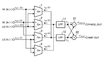
- FIG. 1 is a configuration diagram showing a configuration of an amplitude phase detection circuit according to Embodiment 1.
- FIG. FIG. 2 is a configuration diagram showing the configuration of the amplitude phase detection circuit according to the second embodiment.
- FIG. 3 is a configuration diagram showing the configuration of the amplitude phase detection circuit according to the third embodiment.
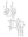
- FIG. 4 is a configuration diagram showing the configuration of an amplitude phase detection circuit according to the fourth embodiment.
- FIG. 5 is a configuration diagram showing the configuration of an amplitude phase detection circuit according to the fifth embodiment.
- FIG. 6 is a configuration diagram showing the configuration of an amplitude phase detection circuit according to the sixth embodiment.
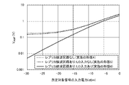
- FIG. 7 is a graph showing an example of simulation comparison results of the amplitude phase detection circuits according to the fourth to sixth embodiments.
- FIG. 1 is a configuration diagram showing a configuration of an amplitude phase detection circuit according to Embodiment 1.
- the amplitude phase detection circuit according to the first embodiment includes a first transconductance element 1, a second transconductance element 2, a third transconductance element 3, a fourth transconductance element 4, and a 1 low-pass filter 11 , a second low-pass filter 12 , a subtractor 21 and an adder 22 .
- the amplitude phase detection circuit according to Embodiment 1 includes four input terminals and two output terminals in addition to the components shown above.
- the four input terminals are represented by RF_IN(+), RF_IN(-), LO_IN(+), and LO_IN(-) on the left side of FIG.
- the two output terminals are represented by PHASE_OUT and AMP_OUT shown on the right side of FIG.
- RF_IN(+) and RF_IN(-) are differential input terminals for the signal to be measured, and the signal to be measured is input as a differential signal.
- LO_IN(+) and LO_IN(-) are differential input terminals for local signals, and local signals are also input as differential signals.
- the local signal is a signal with the same frequency as the signal to be measured.
- PHASE_OUT is a terminal for outputting the phase difference of the signal to be measured with respect to the local signal.
- AMP_OUT is a terminal for outputting the amplitude of the signal to be measured.
- the first transconductance element 1, the second transconductance element 2, the third transconductance element 3, and the fourth transconductance element 4 each have a positive phase input and a negative phase input.
- the positive phase input is indicated by the "+” symbol in FIG.
- the negative phase input is indicated by the "-” symbol in FIG.
- the circuit is configured such that either positive phase input is connected to RF_IN(+) or RF_IN(-) relating to the differential signal of the signal to be measured.
- the circuit is configured such that LO_IN(+) or LO_IN(-) relating to the differential signal of the local signal is connected to any negative phase input.
- each of the four transconductance elements (1 to 4) constitutes a circuit with different combinations of inputs.
- the first transconductance element 1, the second transconductance element 2, the third transconductance element 3, and the fourth transconductance element 4 are all nonlinear elements having the same nonlinear characteristics.
- the transconductance element is exemplified as the nonlinear element here, the nonlinear element may be an element other than the transconductance element.
- a more preferable configuration is that these four transconductance elements (1 to 4) all have the same second-order nonlinear characteristics.
- the positive phase input of the first transconductance element 1 is connected to RF_IN(+), and the negative phase input is connected to LO_IN(+).
- the positive phase input of the second transconductance element 2 is connected to RF_IN(-), and the negative phase input is connected to LO_IN(+).
- the positive phase input of the third transconductance element 3 is connected to RF_IN(-), and the negative phase input is connected to LO_IN(-).
- the positive phase input of the fourth transconductance element 4 is connected to RF_IN(+), and the negative phase input is connected to LO_IN(-).
- All four transconductance elements (1 to 4) output current are indicated in FIG. 1 as id1, id2, id3 and id4, respectively.
- the output current (id 1 ) of the first transconductance element 1 and the output current (id 3 ) of the third transconductance element 3 are combined and sent to the second low-pass filter 12 .
- the output current (id2) of the second transconductance element 2 and the output current (id4) of the fourth transconductance element 4 are combined and sent to the first low-pass filter 11 .
- Both the first low-pass filter 11 and the second low-pass filter 12 block the AC component of the input signal and pass the DC component.
- the passed DC component undergoes current-voltage conversion.
- the DC component that has undergone current-voltage conversion by the first low-pass filter 11 is indicated as Va in FIG.
- the DC component that is current-voltage converted by the second low-pass filter 12 is indicated as Vb in FIG.
- Both the output (Va) of the first low-pass filter 11 and the output (Vb) of the second low-pass filter 12 are sent to the subtractor 21 and the adder 22 .
- the subtractor 21 performs a subtraction process of subtracting the output of the second low-pass filter 12 from the output of the first low-pass filter 11 .
- the result of the subtraction process is output from the PHASE_OUT terminal as a signal containing information about the phase difference.
- the adder 22 adds the output of the first low-pass filter 11 and the output of the second low-pass filter 12 .
- the result of addition processing is output from the AMP_OUT terminal as a signal containing information about amplitude.
- the operating principle of the amplitude phase detection circuit according to the first embodiment is clarified by the following specific formulas.
- the signal to be measured and the local signal are defined by the following formulas representing time waveforms.
- Vr is the amplitude of the signal under measurement
- Vl is the amplitude of the local signal
- ⁇ is the angular frequency of the signal under measurement and the local signal
- ⁇ is the phase difference of the signal under measurement with respect to the local signal.
- variables that take time as an argument are represented by lower-case letters, and constants that do not depend on time are represented by upper-case letters.
- the second-order nonlinear characteristics of the four transconductance elements (1 to 4) are defined by the following formulas. where ⁇ Vin(t) is the voltage obtained by subtracting the negative-phase input from the positive-phase input, iout(t) is the current to be output, and ⁇ , ⁇ , and ⁇ are coefficients representing second-order nonlinear characteristics of the transconductance element. .
- the output currents (id1, id2, id3, id4) of the four transconductance elements (1 to 4) are expressed as follows.
- a composite current of id1 and id3 and a composite current of id2 and id4 are expressed as follows.
- the composite current of id1 and id3 is sent to the second low-pass filter 12, and the composite current of id2 and id4 is sent to the first low-pass filter 11.
- the output (Va) of the first low-pass filter 11 and the output (Vb) of the second low-pass filter 12 are expressed as follows.
- K is a current-voltage conversion coefficient.
- a subtractor 21 subtracts the output (Vb) of the second low-pass filter 12 from the output (Va) of the first low-pass filter 11 .
- the subtraction result (V PHASE ) is expressed as follows.
- the adder 22 adds the output (Va) of the first low-pass filter 11 and the output (Vb) of the second low-pass filter 12 .
- the addition result (V AMP ) is expressed as follows.
- the amplitude (Vr) of the signal to be measured can be obtained from V AMP . Further, from the obtained Vr and V PHASE , the phase difference ( ⁇ ) of the signal to be measured with respect to the local signal can be obtained using the relationship of Equation (7).
- a PHASE_OUT terminal that outputs V PHASE is a terminal that outputs information about the phase of the signal to be measured.
- An AMP_OUT terminal that outputs V AMP is a terminal that outputs information about the amplitude of the signal to be measured.
- the amplitude-phase detection circuit according to Embodiment 1 has the above configuration, it is possible to simultaneously detect the amplitude and phase difference of the signal to be measured with a single circuit without relying on time division.
- Embodiment 1 shows that the amplitude phase detection circuit according to the technique of the present disclosure can obtain the amplitude (Vr) of the signal to be measured from V AMP according to equation (8).
- Equation (8) if the value of the constant term ⁇ of the second-order nonlinear characteristics of the nonlinear element is 0, the amplitude (Vr) can be calculated more easily.
- ⁇ is a value specific to nonlinear elements, its value cannot be changed arbitrarily.
- Embodiment 2 shows that the influence of the constant term ⁇ can be eliminated by adding a certain circuit to the configuration shown in Embodiment 1.
- FIG. 1 shows that the amplitude phase detection circuit according to the technique of the present disclosure can obtain the amplitude (Vr) of the signal to be measured from V AMP according to equation (8).
- Equation (8) if the value of the constant term ⁇ of the second-order nonlinear characteristics of the nonlinear element is 0, the amplitude (Vr) can be calculated more easily.
- ⁇
- FIG. 2 is a configuration diagram showing the configuration of the amplitude phase detection circuit according to the second embodiment.
- the reference numerals used in the second embodiment are the same as those used in the first embodiment except for newly added components. Moreover, in the description of the amplitude phase detection circuit according to the second embodiment, portions that overlap with those of the first embodiment are omitted as appropriate.
- the amplitude phase detection circuit according to the second embodiment has four transconductance elements (5, 6, 7, 8) and a third low-pass filter 13 in addition to the configuration of the first embodiment. , and a second subtractor 23 .
- the four transconductance elements (5, 6, 7, 8) have the same nonlinear characteristics as the transconductance elements (1, 2, 3, 4) according to the first embodiment (see formula (2)).
- the third low-pass filter 13 has the same characteristics as the first low-pass filter 11 and the second low-pass filter 12 according to the first embodiment, and has the same current-voltage conversion coefficient K.
- the four nonlinear elements are represented as four transconductance elements (5, 6, 7, 8) in FIG. 2, the disclosed technique is not limited to this. That is, the four transconductance elements (5, 6, 7, 8) may be the fifth nonlinear element, the sixth nonlinear element, the seventh nonlinear element, and the eighth nonlinear element, respectively.
- the inputs of the four transconductance elements (5, 6, 7, 8) are all connected to GND. All the output currents (id5, id6, id7, id8) of the four transconductance elements (5, 6, 7, 8) are combined and sent to the third low-pass filter 13.
- the output (Vc) of the third low-pass filter 13 is sent to the second subtractor 23 installed after the adder 22 .
- the second subtractor 23 performs a subtraction process of subtracting the output of the third low-pass filter 13 from the output of the adder 22 .
- the principle that the configuration according to the second embodiment can eliminate the influence of the constant term ⁇ will be clarified by the following specific formulas.
- the output currents (id5, id6, id7, id8) of the four transconductance elements (5, 6, 7, 8) are expressed as follows.
- the output (Vc) of the third low-pass filter 13 to which the synthesized current is input is expressed as follows.
- V AMP2 The subtraction result (V AMP2 ) of the second subtractor 23 is expressed as follows.
- the amplitude phase detection circuit according to the second embodiment since the amplitude phase detection circuit according to the second embodiment has the above configuration, it can simultaneously detect the amplitude and the phase difference of the signal to be measured more easily than the first embodiment.
- Embodiment 3 shows that the amplitude phase detection circuit according to the technology disclosed herein can obtain the amplitude (Vr) of the signal to be measured from V AMP2 according to equation (11).
- the amplitude (Vr) of the signal to be measured from V AMP2 As shown in equation (11), the amplitude (Vl) of the local signal must be correctly grasped.
- Embodiment 3 by slightly modifying the configuration shown in Embodiment 2, it is shown that the amplitude (Vr) of the signal to be measured can be obtained without using information on the amplitude (Vl) of the local signal. .
- FIG. 3 is a configuration diagram showing the configuration of the amplitude phase detection circuit according to the third embodiment.
- the reference numerals used in Embodiment 3 are the same as those used in Embodiments 1 and 2, except for newly added components. Also, in the description of the amplitude phase detection circuit according to the third embodiment, portions overlapping those of the first or second embodiment will be omitted as appropriate.
- the opposite phase inputs of the four transconductance elements are connected to different local signals. ing. Specifically, a signal from LO_IN(+) is input to the opposite phase inputs of the fifth transconductance element 5 and the sixth transconductance element 6 . A signal from LO_IN( ⁇ ) is input to the opposite phase inputs of the seventh transconductance element 7 and the eighth transconductance element 8 .
- the principle that the configuration according to the third embodiment does not require information on the amplitude (Vl) of the local signal will be clarified by the following specific formulas.
- the output currents (i d5-3 , i d6-3 , i d7-3 , i d8-3 ) of the four transconductance elements (5-8) are expressed as follows.
- the combined current is expressed as follows.
- the output (V c3 ) of the third low-pass filter 13 to which the synthesized current is input is expressed as follows. From the relationship between equations (6) and (14), the output (V AMP3 ) of the second subtractor 23 can be made without the amplitude (Vl) of the local signal.
- the amplitude-phase detection circuit according to Embodiment 3 has the above configuration, it is possible to simultaneously detect the amplitude and phase difference of the signal to be measured without using information on the amplitude (Vl) of the local signal.
- Embodiment 4 shows a configuration example of realizing an amplitude phase detection circuit according to the technique of the present disclosure using another nonlinear element.
- FIG. 4 is a configuration diagram showing the configuration of the amplitude phase detection circuit according to the fourth embodiment.
- the reference numerals used in the fourth embodiment are the same as those used in the previous embodiments, except for newly appearing components. Also, in the description of the amplitude phase detection circuit according to the fourth embodiment, portions overlapping with those of the previous embodiments will be omitted as appropriate.
- the amplitude phase detection circuit according to the fourth embodiment includes a first transistor 31, a second transistor 32, a third transistor 33, and a fourth transistor 34 as nonlinear elements.
- the amplitude phase detection circuit according to the fourth embodiment further includes inductor 41 .
- Components (101, 102) indicated by broken square lines in FIG. 4 are circuit configurations of the first low-pass filter 11 and the second low-pass filter 12 indicated by blocks in FIGS. 1 to 3 .
- the low pass filter circuits (101, 102) include resistors (51, 54) and capacitors (52, 53), respectively.
- a component (201) indicated by a square dashed line in FIG. 4 is a circuit configuration of the subtractor 21 indicated by a circle indicating subtraction in FIGS. 1 to 3 .
- a component (202) indicated by a square dashed line in FIG. 4 is a circuit configuration of the adder 22 indicated by a circle indicating addition in FIGS.
- the positive phase input and negative phase input of the transconductance elements (1-4) correspond to the gate terminals and source terminals of the transistors (31-34), respectively.
- RF_IN(+) is connected to the gate terminal of the first transistor 31, and LO_IN(+) is connected to the source terminal of the same element.
- the gate terminal of the second transistor 32 is connected to RF_IN(-), and the source terminal of the second transistor 32 is connected to LO_IN(+).
- the gate terminal of the third transistor 33 is connected to RF_IN(-), and the source terminal of the third transistor 33 is connected to LO_IN(-).
- a gate terminal of the fourth transistor 34 is connected to RF_IN(+), and a source terminal of the fourth transistor 34 is connected to LO_IN(-).
- An inductor 41 is connected between the LO_IN(+) terminal and the LO_IN(-) terminal, and its center tap terminal is grounded to GND.
- the outputs of the transconductance elements (1-4) correspond to the drain terminals of the transistors (31-34), respectively.
- the drain terminals of the first transistor 31 and the third transistor 33 are connected to each other and input to a first low-pass filter circuit 101 composed of a parallel connection of a resistor (51) and a capacitor (52).
- the drain terminals of the second transistor 32 and the fourth transistor 34 are connected to each other and input to a second low-pass filter circuit 102 composed of a parallel connection of a resistor (54) and a capacitor (53).
- the first low-pass filter circuit 101 and the second low-pass filter circuit 102 have functions of converting current into voltage and cutting AC components.
- the subtractor circuit 201 is a differential amplifier circuit composed of a subtractor operational amplifier 71 and resistors (61 to 64). output to the terminal.
- the adder circuit 202 is an adder circuit composed of the adder operational amplifier 72 and resistors (65 to 67). output to the terminal.
- the operating principle of the amplitude phase detection circuit according to the fourth embodiment is clarified by the following specific formulas.
- the signal to be measured and the local signal are defined by the following formulas representing time waveforms.
- equation (15) is defined assuming that there is a bias voltage V bias superimposed on the signal to be measured.
- the second-order nonlinear characteristics of the four transistors are defined by the following formulas.
- iD is the drain current flowing through the drain terminal
- VG is the gate voltage
- VS is the source voltage
- Vth is the threshold voltage
- ⁇ is a coefficient relating to the nonlinear characteristics of the transistor.
- drain currents (i D1 , i D2 , i D3 , i D4 ) flowing through the drain terminals of the four transistors are expressed as follows.
- a composite current of i D1 and i D3 and a composite current of i D2 and i D4 are expressed as follows.
- the output (Va) of the first low-pass filter circuit 101 and the output (Vb) of the second low-pass filter circuit 102 are expressed as follows.
- VDD is the power supply voltage
- R is the value of resistors (51, 54).
- V PHASE4 the output voltage of subtractor circuit 201
- V cm the common mode voltage.
- V AMP4 the output voltage of adder circuit 202
- V DD , R, ⁇ , V bias , V th , and Vl are known, so the amplitude (Vr) of the signal to be measured can be obtained from V AMP4 .
- V cm is also known, the phase difference ( ⁇ ) of the signal to be measured with respect to the local signal can be obtained from the obtained Vr and V PHASE4 using the relationship of Equation (21).
- the amplitude phase detection circuit can simultaneously detect the amplitude and phase difference of the signal to be measured with a single circuit without relying on time division.
- Embodiment 5 shows that the influence of the constant term ⁇ can be eliminated by adding a certain circuit to the configuration shown in Embodiment 1.
- FIG. 5 is a configuration diagram showing the configuration of an amplitude phase detection circuit according to the fifth embodiment.
- the reference numerals used in the fifth embodiment are the same as those used in the previous embodiments except for newly added components. Moreover, in the description of the amplitude phase detection circuit according to the fifth embodiment, portions overlapping with those of the previous embodiments will be omitted as appropriate.
- the amplitude phase detection circuit according to the fifth embodiment further includes a replica detection circuit 301 in addition to the configuration of the fourth embodiment.
- a 3-input adder/subtractor circuit 203 is used instead of the adder circuit 202 .
- Replica detection circuit 301 includes four transistors ( 35 , 36 , 37 , 38 ), third low-pass filter circuit 103 , second inductor 42 , and replica capacitor 81 .
- the four transistors (35, 36, 37, 38) have the same nonlinear characteristics as the transistors (31, 32, 33, 34) according to the fourth embodiment (see formula (16)).
- the third low-pass filter circuit 103 is composed of capacitors and resistors having the same values as those of the first low-pass filter circuit 101 and the second low-pass filter circuit 102 according to the fourth embodiment.
- the output of replica detection circuit 301 is connected to one of the three input terminals of 3-input adder/subtractor circuit 203 .
- the gate terminals of the four transistors are grounded through replica capacitors 81, respectively.
- the source terminals of the fifth transistor 35 and the sixth transistor 36 are each connected to one end (the left side in FIG. 5) of the second inductor 42 .
- the source terminals of the seventh transistor 37 and the eighth transistor 38 are connected to the other end (the right side in FIG. 5) of the second inductor 42, respectively.
- a center tap terminal of the second inductor 42 is grounded to GND. Drain terminals of the four transistors (35, 36, 37, 38) are connected to the third low-pass filter circuit 103, respectively.
- the output of the third low-pass filter circuit 103 is the output of the replica detection circuit 301, and is connected to one of the three input terminals of the 3-input adder/subtractor circuit 203 as described above.
- the drain currents (i D5 , i D6 , i D7 , i D8 ) of the four transistors (35-38) are expressed as follows.
- the output (V c5 ) of the third low-pass filter circuit 103 is expressed as follows.
- the resistance value of the 3-input adder/subtractor circuit 203 is determined so that the output (V AMP5 ) satisfies the following equation. Substituting the relationship between equations (20) and (24) into equation (25), the output (V AMP5 ) of the circuit shown in FIG. 5 is expressed as follows.
- the amplitude-phase detection circuit according to the fifth embodiment since the amplitude-phase detection circuit according to the fifth embodiment has the above configuration, it can simultaneously detect the amplitude and the phase difference of the signal to be measured more easily than the circuit according to the fourth embodiment.
- Embodiment 3 shows that the amplitude (Vr) of the signal to be measured can be obtained without using information on the amplitude (Vl) of the local signal by slightly modifying the configuration shown in Embodiment 2. ing. Similarly, in the sixth embodiment, by slightly modifying the configuration shown in the fifth embodiment, the amplitude (Vr) of the signal to be measured can be obtained without using the information on the amplitude (Vl) of the local signal. shown.
- FIG. 6 is a configuration diagram showing the configuration of the amplitude phase detection circuit according to the sixth embodiment.
- the reference numerals used in the sixth embodiment are the same as those used in the previous embodiments, except for newly added components. Also, in the description of the amplitude phase detection circuit according to the sixth embodiment, portions overlapping with those of the previous embodiments will be omitted as appropriate.
- the connection destinations of the source terminals of the four transistors (35 to 38) are changed so that local signals are input. Specifically, a signal from LO_IN(+) is input to the source terminals of the fifth transistor 35 and the sixth transistor 36 . A signal from LO_IN( ⁇ ) is input to the source terminals of the seventh transistor 37 and the eighth transistor 38 .
- the principle that the configuration according to the sixth embodiment does not require the information of the amplitude (Vl) of the local signal will be clarified by the following specific formulas.
- the output currents (i D5-6 , i D6-6 , i D7-6 , i D8-6 ) of the four transistors (35-38) are expressed as follows.
- a combined current in the circuit configuration of FIG. 6 is expressed as follows.
- the output (V c6 ) of the third low-pass filter circuit 103 is expressed as follows.
- the amplitude phase detection circuit according to Embodiment 6 has the above configuration, it is possible to simultaneously detect the amplitude and phase difference of the signal to be measured without using information on the amplitude (Vl) of the local signal.
- FIG. 7 is a graph showing an example of simulation comparison results of the amplitude phase detection circuits according to the fourth to sixth embodiments.
- the configuration of the fourth embodiment without the replica detection circuit 301 is easily affected by V bias and Vl when the input power of the signal to be measured is small.
- the linear characteristics are slightly improved by eliminating the influence of V bias .
- FIG. 7 shows that the adoption of the configuration of Embodiment 6 can improve the linear characteristic with respect to the input power of the signal to be measured.
- the technology disclosed herein can be applied to detection circuits of phased array antennas used in radar and communication devices, and has industrial applicability.
- first to eighth transconductance elements 11 to 13 first to third low-pass filters, 21 subtractor, 22 adder, 23 second subtractor, 31 to 38 first to eighth transistors, 41 inductor, 42 second inductor, 71 subtractor operational amplifier, 72 adder operational amplifier, 81 replica capacitor, 101 to 103 first to third low-pass filter circuits, 201 subtractor circuit, 202 adder circuit, 203 3-input adder/subtractor circuit, 301 Replica detection circuit.
Landscapes
- Engineering & Computer Science (AREA)
- Power Engineering (AREA)
- Measuring Phase Differences (AREA)
Abstract
本開示技術に係る振幅位相検波回路は、入力側から順に、少なくとも2組の差動入力端子、4つの非線形素子(1~4又は31~34)、2つのローパスフィルタ(11~12又は101~102)、加算器(22又は72)、減算器(21又は71)、を含む。
Description
本開示技術は、振幅位相検波回路に関する。
一般に信号の振幅と位相とを求める方法として、測定対象信号をAD変換し、AD変換されたデジタルデータに対して信号処理を行うことが考えられる。しかし取り扱う信号がマイクロ波帯及びミリ波帯等である場合、非常に高速なAD変換を行う必要がありこの方法は現実的ではない。取り扱う信号がマイクロ波帯及びミリ波帯等である場合は、アナログ的な振幅位相検波回路がよく用いられる。
振幅位相検波回路が用いられている製品の一例として、フェーズドアレーアンテナが知られている。フェーズドアレーアンテナはレーダや通信装置に使用されるアンテナ群であって、送信する電波(以下、「送信ビーム」という)の放射方向を制御できる性質を有する。フェーズドアレーアンテナの各アンテナは直線上又は円周上に配列され、ある任意の方向で同相に加わり合うように各アンテナ素子から出力する電波の位相を調整することにより、その方向に対して強い指向性を持つ。アンテナ素子へ供給される送信RF信号の振幅と位相は、可変利得増幅器及び移相器を用いて調整される場合と、各アンテナ素子にそれぞれ独立な発振器を接続し発振位相を制御する場合とがある。
アンテナ素子へ供給される送信RF信号のばらつきをなくすため、供給される信号の一部を取り出してフィードバック制御することが行われている。取り出した信号の測定は、振幅検波回路と位相検波回路とが用いられる。また、回路規模の増大を抑えるという目的で、信号の位相と振幅とを1つの回路で実現した振幅位相検波回路も開示されている(例えば特許文献1)。
特許文献1に係る振幅位相検波回路は、基準信号の位相を0°変化させて出力する第1の状態、基準信号の位相を90°変化させて出力する第2の状態、及び基準信号の通過を遮断する第3の状態の3つの状態を順に切り替えて動作するスイッチを備える。特許文献1に係る振幅位相検波回路は、第1の状態又は第2の状態の場合に基準信号と測定対象信号との位相差を算出し、第3の状態の場合に測定対象信号の振幅を算出している。より簡単に言えば、特許文献1に係る振幅位相検波回路は、時分割により位相と振幅の検波を実現している。
振幅位相検波回路は、算出する振幅と位相差とがあまり変化しない場合には従来の時分割方式の検波を採用してもさほど問題とはならない。しかし状況により振幅位相検波回路は、1つの回路で測定対象信号の振幅と位相差とを同時に検出することが望まれる。本開示技術はこの課題を解決し、時分割に頼らず1つの回路で測定対象信号の振幅と位相差とを同時に検出する振幅位相検波回路の提供を目的とする。
本開示技術に係る振幅位相検波回路は、入力側から順に、少なくとも2組の差動入力端子、4つの非線形素子、2つのローパスフィルタ、加算器、減算器、を含む。
本開示技術に係る振幅位相検波回路は上記構成を備えるため、時分割に頼らず1つの回路で測定対象信号の振幅と位相差とを同時に検出できる。
本開示技術に係る振幅位相検波回路は、以下の実施の形態ごとの図面に沿った説明により明らかにされる。
実施の形態1.
図1は、実施の形態1に係る振幅位相検波回路の構成を示す構成図である。図1が示すとおり実施の形態1に係る振幅位相検波回路は、第1トランスコンダクタンス素子1と、第2トランスコンダクタンス素子2と、第3トランスコンダクタンス素子3と、第4トランスコンダクタンス素子4と、第1ローパスフィルタ11と、第2ローパスフィルタ12と、減算器21と、加算器22と、を含む。
図1は、実施の形態1に係る振幅位相検波回路の構成を示す構成図である。図1が示すとおり実施の形態1に係る振幅位相検波回路は、第1トランスコンダクタンス素子1と、第2トランスコンダクタンス素子2と、第3トランスコンダクタンス素子3と、第4トランスコンダクタンス素子4と、第1ローパスフィルタ11と、第2ローパスフィルタ12と、減算器21と、加算器22と、を含む。
図1が示すとおり実施の形態1に係る振幅位相検波回路は上記に示した構成要素に加え、4つの入力端子と、2つの出力端子と、を含む。4つの入力端子は、図1の左側に記載されたRF_IN(+)、RF_IN(-)、LO_IN(+)、及びLO_IN(-)で表されている。2つの出力端子は、図1の右側に記載されたPHASE_OUT、及びAMP_OUTで表されている。RF_IN(+)とRF_IN(-)は測定対象信号のための差動入力端子であり、測定対象信号は差動信号として入力される。LO_IN(+)とLO_IN(-)はローカル信号のための差動入力端子であり、ローカル信号も差動信号として入力される。ローカル信号は、測定対象信号と同じ周波数の信号である。PHASE_OUTは、測定対象信号のローカル信号に対する位相差を出力するための端子である。AMP_OUTは、測定対象信号の振幅を出力するための端子である。
第1トランスコンダクタンス素子1、第2トランスコンダクタンス素子2、第3トランスコンダクタンス素子3、及び第4トランスコンダクタンス素子4は、それぞれ正相入力と逆相入力とを有する。正相入力は、図1において「+」の記号で示されている。逆相入力は、図1において「-」の記号で示されている。いずれの正相入力も、測定対象信号の差動信号に関するRF_IN(+)又はRF_IN(-)が接続されるように回路が構成されている。またいずれの逆相入力も、ローカル信号の差動信号に関するLO_IN(+)又はLO_IN(-)が接続されるように回路が構成されている。{RF_IN(+)、RF_IN(-)}から1つを選び、{LO_IN(+)、LO_IN(-)}から1つを選ぶ組合せは全部で4通りである。4つのトランスコンダクタンス素子(1~4)は、いずれも異なった入力の組合せで回路が構成されている。
また、第1トランスコンダクタンス素子1、第2トランスコンダクタンス素子2、第3トランスコンダクタンス素子3、及び第4トランスコンダクタンス素子4は、いずれも同じ非線形特性を有する非線形素子である。ここでは非線形素子としてトランスコンダクタンス素子を例示したが、非線形素子はトランスコンダクタンス素子以外の素子でもよい。より好ましい構成は、これら4つのトランスコンダクタンス素子(1~4)がいずれも同じ2次非線形特性を有することである。本開示技術に係る振幅位相検波回路が非線形特性を有する素子を採用する理由は、後述の動作原理の説明により明らかにされる。
また、第1トランスコンダクタンス素子1、第2トランスコンダクタンス素子2、第3トランスコンダクタンス素子3、及び第4トランスコンダクタンス素子4は、いずれも同じ非線形特性を有する非線形素子である。ここでは非線形素子としてトランスコンダクタンス素子を例示したが、非線形素子はトランスコンダクタンス素子以外の素子でもよい。より好ましい構成は、これら4つのトランスコンダクタンス素子(1~4)がいずれも同じ2次非線形特性を有することである。本開示技術に係る振幅位相検波回路が非線形特性を有する素子を採用する理由は、後述の動作原理の説明により明らかにされる。
図1の例では、第1トランスコンダクタンス素子1の正相入力はRF_IN(+)と接続され、逆相入力はLO_IN(+)が接続されている。第2トランスコンダクタンス素子2の正相入力はRF_IN(-)と接続され、逆相入力はLO_IN(+)が接続されている。第3トランスコンダクタンス素子3の正相入力はRF_IN(-)と接続され、逆相入力はLO_IN(-)が接続されている。第4トランスコンダクタンス素子4の正相入力はRF_IN(+)と接続され、逆相入力はLO_IN(-)が接続されている。
4つのトランスコンダクタンス素子(1~4)は、いずれも電流を出力する。4つのトランスコンダクタンス素子(1~4)の出力電流は、図1においてそれぞれ順にid1、id2、id3、及びid4と示されている。第1トランスコンダクタンス素子1の出力電流(id1)と第3トランスコンダクタンス素子3の出力電流(id3)とは、合成され、第2ローパスフィルタ12へ送られる。第2トランスコンダクタンス素子2の出力電流(id2)と第4トランスコンダクタンス素子4の出力電流(id4)とは、合成され、第1ローパスフィルタ11へ送られる。
第1ローパスフィルタ11及び第2ローパスフィルタ12は、いずれも入力された信号のAC成分を遮断し、DC成分を通過させる。通過したDC成分は、電流電圧変換がなされる。第1ローパスフィルタ11で電流電圧変換がなされたDC成分は、図1においてVaと示されている。第2ローパスフィルタ12で電流電圧変換がなされたDC成分は、図1においてVbと示されている。
第1ローパスフィルタ11の出力(Va)と第2ローパスフィルタ12の出力(Vb)とは、いずれも減算器21と加算器22とへ送られる。減算器21は、第1ローパスフィルタ11の出力から第2ローパスフィルタ12の出力を減算する減算処理を行う。減算処理結果は、PHASE_OUT端子より位相差に関する情報を含む信号として出力される。加算器22は、第1ローパスフィルタ11の出力と第2ローパスフィルタ12の出力との加算処理を行う。加算処理結果は、AMP_OUT端子より振幅に関する情報を含む信号として出力される。
実施の形態1に係る振幅位相検波回路の動作原理は、以下の具体的な数式により明らかにされる。測定対象信号及びローカル信号は、以下の時間波形を表す数式で定義される。
 ここで、Vrは測定対象信号の振幅、Vlはローカル信号の振幅、ωは測定対象信号及びローカル信号の角周波数、φはローカル信号に対する測定対象信号の位相差、をそれぞれ表す。以降、時間を引数とする変数は小文字アルファベットで表され、時間に依存しない定数等は大文字アルファベットで表される。
4つのトランスコンダクタンス素子(1~4)が有する2次非線形特性は、以下の数式で定義される。
 ここでΔVin(t)は正相入力から逆相入力を引いた電圧、iout(t)は出力される電流、α、β、γはトランスコンダクタンス素子が有する2次非線形特性を表す係数、である。
具体的に4つのトランスコンダクタンス素子(1~4)の出力電流(id1、id2、id3、id4)は、以下のように表される。

id1とid3との合成電流、id2とid4との合成電流は、以下のように表される。


id1とid3との合成電流は第2ローパスフィルタ12へ送付され、id2とid4との合成電流は第1ローパスフィルタ11へ送付される。第1ローパスフィルタ11の出力(Va)と第2ローパスフィルタ12の出力(Vb)とは、それぞれ以下のように表される。
 ただしKは、電流電圧変換係数である。
減算器21は、第1ローパスフィルタ11の出力(Va)から第2ローパスフィルタ12の出力(Vb)を減算する。減算結果(VPHASE)は、以下のように表される。
 加算器22は、第1ローパスフィルタ11の出力(Va)と第2ローパスフィルタ12の出力(Vb)との加算処理を行う。加算結果(VAMP)は、以下のように表される。

式(8)においてK、α、Vl、γは既知であるため、VAMPから測定対象信号の振幅(Vr)を求めることができる。さらに求めたVrとVPHASEとから、式(7)の関係を用いて測定対象信号のローカル信号に対する位相差(φ)を求めることができる。
VPHASEを出力するPHASE_OUT端子は、測定対象信号の位相に関する情報を出力する端子である。またVAMPを出力するAMP_OUT端子は、測定対象信号の振幅に関する情報を出力する端子である。
以上のとおり実施の形態1に係る振幅位相検波回路は上記構成を備えるため、時分割に頼らず1つの回路で測定対象信号の振幅と位相差とを同時に検出できる。
実施の形態2.
実施の形態1では、本開示技術に係る振幅位相検波回路が式(8)に従ってVAMPから測定対象信号の振幅(Vr)を求められることが示されている。式(8)が示すように非線形素子が有する2次非線形特性のうちの定数項γは、値が0であれば振幅(Vr)の算出がより容易になる。ただしγは非線形素子に固有の値であるため、任意に値を変更することはできない。
実施の形態2では、実施の形態1で示された構成に或る回路を追加することで、定数項γの影響を排除できることが示される。
実施の形態1では、本開示技術に係る振幅位相検波回路が式(8)に従ってVAMPから測定対象信号の振幅(Vr)を求められることが示されている。式(8)が示すように非線形素子が有する2次非線形特性のうちの定数項γは、値が0であれば振幅(Vr)の算出がより容易になる。ただしγは非線形素子に固有の値であるため、任意に値を変更することはできない。
実施の形態2では、実施の形態1で示された構成に或る回路を追加することで、定数項γの影響を排除できることが示される。
図2は、実施の形態2に係る振幅位相検波回路の構成を示す構成図である。実施の形態2で用いる符号は、あらたに追加された構成要素を除き実施の形態1で用いたものが用いられている。また、実施の形態2に係る振幅位相検波回路の説明において、実施の形態1と重複する部分は、適宜省略される。
図2が示すとおり実施の形態2に係る振幅位相検波回路は、実施の形態1の構成に加えて、さらに4つのトランスコンダクタンス素子(5、6、7、8)と、第3ローパスフィルタ13と、第2減算器23と、を含む。ここで4つのトランスコンダクタンス素子(5、6、7、8)は、実施の形態1に係るトランスコンダクタンス素子(1、2、3、4)と同じ非線形特性を有する(式(2)参照)。また、第3ローパスフィルタ13は、実施の形態1に係る第1ローパスフィルタ11及び第2ローパスフィルタ12と同じ特性を有し、電流電圧変換係数も同じKである。
図2では4つの非線形素子を4つのトランスコンダクタンス素子(5、6、7、8)として表したが、本開示技術はこれに限定されない。すなわち4つのトランスコンダクタンス素子(5、6、7、8)は、それぞれ第5非線形素子、第6非線形素子、第7非線形素子、及び第8非線形素子であってもよい。
図2では4つの非線形素子を4つのトランスコンダクタンス素子(5、6、7、8)として表したが、本開示技術はこれに限定されない。すなわち4つのトランスコンダクタンス素子(5、6、7、8)は、それぞれ第5非線形素子、第6非線形素子、第7非線形素子、及び第8非線形素子であってもよい。
4つのトランスコンダクタンス素子(5、6、7、8)の入力は、いずれもGNDに接続されている。4つのトランスコンダクタンス素子(5、6、7、8)の出力電流(id5、id6、id7、id8)はすべて合成され、第3ローパスフィルタ13へ送られる。第3ローパスフィルタ13の出力(Vc)は、加算器22の後段に設置された第2減算器23へ送られる。第2減算器23は、加算器22の出力から第3ローパスフィルタ13の出力を減算する減算処理を行う。
実施の形態2に係る構成が定数項γの影響を排除できる原理は、以下の具体的な数式により明らかにされる。4つのトランスコンダクタンス素子(5、6、7、8)の出力電流(id5、id6、id7、id8)は、以下のように表される。

合成電流が入力された第3ローパスフィルタ13の出力(Vc)は、以下のように表される。

第2減算器23の減算結果(VAMP2)は、以下のように表される。

以上のとおり実施の形態2に係る振幅位相検波回路は上記構成を備えるため、実施の形態1のものよりも容易に測定対象信号の振幅と位相差とを同時に検出できる。
実施の形態3.
実施の形態2では、本開示技術に係る振幅位相検波回路が式(11)に従ってVAMP2から測定対象信号の振幅(Vr)を求められることが示されている。式(11)が示すようにVAMP2から測定対象信号の振幅(Vr)を求めるには、ローカル信号の振幅(Vl)を正しく把握しなければならない。
実施の形態3では、実施の形態2で示された構成を少し変形することで、ローカル信号の振幅(Vl)の情報を用いることなく測定対象信号の振幅(Vr)が求められることが示される。
実施の形態2では、本開示技術に係る振幅位相検波回路が式(11)に従ってVAMP2から測定対象信号の振幅(Vr)を求められることが示されている。式(11)が示すようにVAMP2から測定対象信号の振幅(Vr)を求めるには、ローカル信号の振幅(Vl)を正しく把握しなければならない。
実施の形態3では、実施の形態2で示された構成を少し変形することで、ローカル信号の振幅(Vl)の情報を用いることなく測定対象信号の振幅(Vr)が求められることが示される。
図3は、実施の形態3に係る振幅位相検波回路の構成を示す構成図である。実施の形態3で用いる符号は、あらたに追加された構成要素を除き実施の形態1及び実施の形態2で用いたものが用いられている。また、実施の形態3に係る振幅位相検波回路の説明において、実施の形態1又は実施の形態2と重複する部分は、適宜省略される。
図3が示すとおり実施の形態3に係る振幅位相検波回路では、4つのトランスコンダクタンス素子(5、6、7、8)の逆相入力は、それぞれローカル信号が入力されるよう接続先が変更されている。具体的には第5トランスコンダクタンス素子5と第6トランスコンダクタンス素子6の逆相入力にはLO_IN(+)からの信号が入力される。また第7トランスコンダクタンス素子7と第8トランスコンダクタンス素子8の逆相入力にはLO_IN(-)からの信号が入力される。
実施の形態3に係る構成がローカル信号の振幅(Vl)の情報を不要とする原理は、以下の具体的な数式により明らかにされる。4つのトランスコンダクタンス素子(5~8)の出力電流(id5-3、id6-3、id7-3、id8-3)は、以下のように表される。

合成電流は、以下のように表される。

合成電流が入力された第3ローパスフィルタ13の出力(Vc3)は、以下のように表される。
 式(6)と式(14)との関係から、第2減算器23の出力(VAMP3)はローカル信号の振幅(Vl)を含まない形にすることができる。
以上のとおり実施の形態3に係る振幅位相検波回路は上記構成を備えるため、ローカル信号の振幅(Vl)の情報を用いることなく測定対象信号の振幅と位相差とを同時に検出できる。
実施の形態4.
実施の形態1から実施の形態3は、本開示技術に係る振幅位相検波回路における非線形素子をトランスコンダクタンス素子(1~8)で実現した構成例を示した。
実施の形態4は、別の非線形素子を用いて本開示技術に係る振幅位相検波回路を実現する構成例を示す。
実施の形態1から実施の形態3は、本開示技術に係る振幅位相検波回路における非線形素子をトランスコンダクタンス素子(1~8)で実現した構成例を示した。
実施の形態4は、別の非線形素子を用いて本開示技術に係る振幅位相検波回路を実現する構成例を示す。
図4は、実施の形態4に係る振幅位相検波回路の構成を示す構成図である。実施の形態4で用いる符号は、あらたに登場する構成要素を除き既出の実施の形態で用いたものが用いられている。また、実施の形態4に係る振幅位相検波回路の説明において、既出の実施の形態と重複する部分は、適宜省略される。
図4が示すとおり実施の形態4に係る振幅位相検波回路は、非線形素子として、第1トランジスタ31と、第2トランジスタ32と、第3トランジスタ33と、第4トランジスタ34と、を含む。
実施の形態4に係る振幅位相検波回路は、さらにインダクタ41を含む。
実施の形態4に係る振幅位相検波回路は、さらにインダクタ41を含む。
図4における四角い破線で示した構成要素(101、102)は、図1から図3ではブロックで示された第1ローパスフィルタ11及び第2ローパスフィルタ12を回路構成で示したものである。図4が示すとおりローパスフィルタ回路(101、102)は、それぞれ抵抗(51、54)と、コンデンサ(52、53)と、を含む。
図4における四角い破線で示した構成要素(201)は、図1から図3では減算を示す円で示された減算器21を回路構成で示したものである。また図4における四角い破線で示した構成要素(202)は、図1から図3では加算を示す円で示された加算器22を回路構成で示したものである。
トランスコンダクタンス素子(1~4)の正相入力と逆相入力とは、それぞれトランジスタ(31~34)のゲート端子とソース端子とに該当する。
図4の例では、第1トランジスタ31のゲート端子はRF_IN(+)が接続され、同素子のソース端子はLO_IN(+)が接続されている。第2トランジスタ32のゲート端子はRF_IN(-)が接続され、同素子のソース端子はLO_IN(+)が接続されている。第3トランジスタ33のゲート端子はRF_IN(-)が接続され、同素子のソース端子はLO_IN(-)が接続されている。第4トランジスタ34のゲート端子はRF_IN(+)が接続され、同素子のソース端子はLO_IN(-)が接続されている。
LO_IN(+)端子とLO_IN(-)端子との間にはインダクタ41が接続され、そのセンタータップ端子はGND接地されている。
図4の例では、第1トランジスタ31のゲート端子はRF_IN(+)が接続され、同素子のソース端子はLO_IN(+)が接続されている。第2トランジスタ32のゲート端子はRF_IN(-)が接続され、同素子のソース端子はLO_IN(+)が接続されている。第3トランジスタ33のゲート端子はRF_IN(-)が接続され、同素子のソース端子はLO_IN(-)が接続されている。第4トランジスタ34のゲート端子はRF_IN(+)が接続され、同素子のソース端子はLO_IN(-)が接続されている。
LO_IN(+)端子とLO_IN(-)端子との間にはインダクタ41が接続され、そのセンタータップ端子はGND接地されている。
トランスコンダクタンス素子(1~4)の出力は、それぞれトランジスタ(31~34)のドレイン端子が該当する。
第1トランジスタ31と第3トランジスタ33それぞれのドレイン端子は互いに接続され、抵抗(51)とコンデンサ(52)の並列接続で構成される第1ローパスフィルタ回路101に入力される。第2トランジスタ32と第4トランジスタ34それぞれのドレイン端子は互いに接続され、抵抗(54)とコンデンサ(53)の並列接続で構成される第2ローパスフィルタ回路102に入力される。
第1ローパスフィルタ回路101と第2ローパスフィルタ回路102とは、それぞれ電流を電圧に変換するとともにAC成分をカットする機能を有する。
第1トランジスタ31と第3トランジスタ33それぞれのドレイン端子は互いに接続され、抵抗(51)とコンデンサ(52)の並列接続で構成される第1ローパスフィルタ回路101に入力される。第2トランジスタ32と第4トランジスタ34それぞれのドレイン端子は互いに接続され、抵抗(54)とコンデンサ(53)の並列接続で構成される第2ローパスフィルタ回路102に入力される。
第1ローパスフィルタ回路101と第2ローパスフィルタ回路102とは、それぞれ電流を電圧に変換するとともにAC成分をカットする機能を有する。
減算器回路201は減算器用オペアンプ71と抵抗(61~64)で構成される差動増幅回路であり、第1ローパスフィルタ回路101の出力と第2ローパスフィルタ回路102の出力の電圧減算結果がPHASE_OUT端子へ出力される。また加算器回路202は加算器用オペアンプ72と抵抗(65~67)で構成される加算回路であり、第1ローパスフィルタ回路101の出力と第2ローパスフィルタ回路102の出力との電圧加算結果がAMP_OUT端子へ出力される。
実施の形態4に係る振幅位相検波回路の動作原理は、以下の具体的な数式により明らかにされる。測定対象信号及びローカル信号は、以下の時間波形を表す数式で定義される。
 式(1)とは異なり式(15)は、測定対象信号に重畳されたバイアス電圧Vbiasがあるものとして定義されている。
4つのトランジスタが有する2次非線形特性は、以下の数式で定義される。
 ここでiDはドレイン端子を流れるドレイン電流、VGはゲート電圧、VSはソース電圧、Vthは閾値電圧、δはトランジスタの非線形特性に関する係数である。
具体的に4つのトランジスタのドレイン端子を流れるドレイン電流(iD1、iD2、iD3、iD4)は、以下のように表される。

iD1とiD3との合成電流、iD2とiD4との合成電流は、以下のように表される。
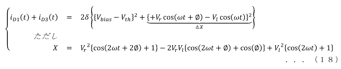

図4に示す回路においては、第1ローパスフィルタ回路101の出力(Va)と第2ローパスフィルタ回路102の出力(Vb)とは、それぞれ以下のように表される。
 ただしVDDは電源電圧、Rは抵抗(51、54)の値、である。
抵抗(61~64)の値が等しく、かつ、その値が十分大きいと仮定すると、減算器回路201の出力電圧(VPHASE4)は、以下の式で表される。
 ただしVcmは同相電圧である。
抵抗(65~67)の値が等しく、かつ、その値が十分大きいと仮定すると、加算器回路202の出力電圧(VAMP4)は、以下の式で表される。

抵抗(65~67)の値が等しく、かつ、その値が十分大きいと仮定すると、加算器回路202の出力電圧(VAMP4)は、以下の式で表される。
式(22)において、VDD、R、δ、Vbias、Vth、Vlは既知であるため、VAMP4から測定対象信号の振幅(Vr)を求めることができる。さらにVcmも既知であるため、求めたVrとVPHASE4とから、式(21)の関係を用いて測定対象信号のローカル信号に対する位相差(φ)を求めることができる。
以上のとおり実施の形態4に係る回路構成を用いても、本開示技術に係る振幅位相検波回路は、時分割に頼らず1つの回路で測定対象信号の振幅と位相差とを同時に検出できる。
実施の形態5.
実施の形態2では、実施の形態1で示された構成に或る回路を追加することで、定数項γの影響を排除できることが示されている。
同様に実施の形態5は、実施の形態4で示された構成に或る回路を追加することで、VbiasとVthとの影響を排除できることが示される。
実施の形態2では、実施の形態1で示された構成に或る回路を追加することで、定数項γの影響を排除できることが示されている。
同様に実施の形態5は、実施の形態4で示された構成に或る回路を追加することで、VbiasとVthとの影響を排除できることが示される。
図5は、実施の形態5に係る振幅位相検波回路の構成を示す構成図である。実施の形態5で用いる符号は、あらたに追加された構成要素を除き既出の実施の形態で用いたものが用いられている。また、実施の形態5に係る振幅位相検波回路の説明において、既出の実施の形態と重複する部分は、適宜省略される。
図5が示すとおり実施の形態5に係る振幅位相検波回路は、実施の形態4の構成に加えて、レプリカ検波回路301をさらに含む。また実施の形態5は、加算器回路202に代えて3入力加減算器回路203が用いられている。
レプリカ検波回路301は、4つのトランジスタ(35、36、37、38)と、第3ローパスフィルタ回路103と、第2インダクタ42と、レプリカ用コンデンサ81と、を含む。ここで4つのトランジスタ(35、36、37、38)は、実施の形態4に係るトランジスタ(31、32、33、34)と同じ非線形特性を有する(式(16)参照)。また、第3ローパスフィルタ回路103は、実施の形態4に係る第1ローパスフィルタ回路101及び第2ローパスフィルタ回路102と同じ値のコンデンサ及び抵抗により構成されている。
レプリカ検波回路301の出力は、3入力加減算器回路203の3つの入力端子のうちの1つの入力端子へ接続されている。
レプリカ検波回路301は、4つのトランジスタ(35、36、37、38)と、第3ローパスフィルタ回路103と、第2インダクタ42と、レプリカ用コンデンサ81と、を含む。ここで4つのトランジスタ(35、36、37、38)は、実施の形態4に係るトランジスタ(31、32、33、34)と同じ非線形特性を有する(式(16)参照)。また、第3ローパスフィルタ回路103は、実施の形態4に係る第1ローパスフィルタ回路101及び第2ローパスフィルタ回路102と同じ値のコンデンサ及び抵抗により構成されている。
レプリカ検波回路301の出力は、3入力加減算器回路203の3つの入力端子のうちの1つの入力端子へ接続されている。
4つのトランジスタ(35、36、37、38)のゲート端子は、それぞれレプリカ用コンデンサ81を介してGND接地されている。
第5トランジスタ35と第6トランジスタ36のソース端子は、それぞれ第2インダクタ42の一端(図5では左側)に接続されている。第7トランジスタ37と第8トランジスタ38のソース端子は、それぞれ第2インダクタ42の他端(図5では右側)に接続されている。
第2インダクタ42のセンタータップ端子は、GND接地されている。
4つのトランジスタ(35、36、37、38)のドレイン端子は、それぞれ第3ローパスフィルタ回路103に接続されている。
第5トランジスタ35と第6トランジスタ36のソース端子は、それぞれ第2インダクタ42の一端(図5では左側)に接続されている。第7トランジスタ37と第8トランジスタ38のソース端子は、それぞれ第2インダクタ42の他端(図5では右側)に接続されている。
第2インダクタ42のセンタータップ端子は、GND接地されている。
4つのトランジスタ(35、36、37、38)のドレイン端子は、それぞれ第3ローパスフィルタ回路103に接続されている。
第3ローパスフィルタ回路103の出力はレプリカ検波回路301の出力であり、前述のとおり3入力加減算器回路203の3つの入力端子のうちの1つの入力端子へ接続されている。
実施の形態5に係る構成がVbiasとVthとの影響を排除できる原理は、以下の具体的な数式により明らかにされる。4つのトランジスタ(35~38)のドレイン電流(iD5、iD6、iD7、iD8)は、以下のように表される。

図5に示す回路において、第3ローパスフィルタ回路103の出力(Vc5)は、以下のように表される。

3入力加減算器回路203は、出力(VAMP5)が以下の等式が成り立つように抵抗値を決めておく。
 式(20)と式(24)との関係を式(25)へ代入すれば、図5に示す回路の出力(VAMP5)は、以下のように表される。

以上のとおり実施の形態5に係る振幅位相検波回路は上記構成を備えるため、実施の形態4のものよりも容易に測定対象信号の振幅と位相差とを同時に検出できる。
実施の形態6.
実施の形態3では、実施の形態2で示された構成を少し変形することで、ローカル信号の振幅(Vl)の情報を用いることなく測定対象信号の振幅(Vr)が求められることが示されている。
同様に実施の形態6は、実施の形態5で示された構成を少し変形することで、ローカル信号の振幅(Vl)の情報を用いることなく測定対象信号の振幅(Vr)が求められることが示される。
実施の形態3では、実施の形態2で示された構成を少し変形することで、ローカル信号の振幅(Vl)の情報を用いることなく測定対象信号の振幅(Vr)が求められることが示されている。
同様に実施の形態6は、実施の形態5で示された構成を少し変形することで、ローカル信号の振幅(Vl)の情報を用いることなく測定対象信号の振幅(Vr)が求められることが示される。
図6は、実施の形態6に係る振幅位相検波回路の構成を示す構成図である。実施の形態6で用いる符号は、あらたに追加された構成要素を除き既出の実施の形態で用いたものが用いられている。また、実施の形態6に係る振幅位相検波回路の説明において、既出の実施の形態と重複する部分は、適宜省略される。
図6が示すとおり実施の形態6に係る振幅位相検波回路では、4つのトランジスタ(35~38)のソース端子は、それぞれローカル信号が入力されるよう接続先が変更されている。具体的には第5トランジスタ35と第6トランジスタ36のソース端子にはLO_IN(+)からの信号が入力される。また第7トランジスタ37と第8トランジスタ38のソース端子にはLO_IN(-)からの信号が入力される。
実施の形態6に係る構成がローカル信号の振幅(Vl)の情報を不要とする原理は、以下の具体的な数式により明らかにされる。4つのトランジスタ(35~38)の出力電流(iD5-6、iD6-6、iD7-6、iD8-6)は、以下のように表される。

図6の回路構成における合成電流は、以下のように表される。

図6に示す回路において、第3ローパスフィルタ回路103の出力(Vc6)は、以下のように表される。

式(20)と式(29)との関係から、図6に示す回路の出力(VAMP6)は、以下のように表される。

以上のとおり実施の形態6に係る振幅位相検波回路は上記構成を備えるため、ローカル信号の振幅(Vl)の情報を用いることなく測定対象信号の振幅と位相差とを同時に検出できる。
図7は、実施の形態4~6に係る振幅位相検波回路のシミュレーション比較結果の一例を示したグラフである。図7が示すとおり、レプリカ検波回路301がない実施の形態4の構成では測定対象信号の入力電力が小さい場合VbiasとVlの影響を受け易い。実施の形態5の構成では、Vbiasの影響を排除した分だけ、若干線形特性が改善されている。図7は、実施の形態6の構成を採用することにより、測定対象信号の入力電力に対する線形特性を改善できることを示している。
本開示技術は、レーダや通信装置に使用されるフェーズドアレーアンテナの検波回路に応用でき、産業上の利用可能性を有する。
1~8 第1~第8トランスコンダクタンス素子、 11~13 第1~第3ローパスフィルタ、 21 減算器、 22 加算器、 23 第2減算器、 31~38 第1~第8トランジスタ、 41 インダクタ、 42 第2インダクタ、 71 減算器用オペアンプ、 72 加算器用オペアンプ、 81 レプリカ用コンデンサ、 101~103 第1~第3ローパスフィルタ回路、 201 減算器回路、 202 加算器回路、 203 3入力加減算器回路、 301 レプリカ検波回路。
Claims (5)
- 入力側から順に、少なくとも2組の差動入力端子、4つの非線形素子、2つのローパスフィルタ、加算器、減算器、を含む振幅位相検波回路。
- 上流から順に、
前記非線形素子と同じ特性を有する第5非線形素子、第6非線形素子、第7非線形素子、及び第8非線形素子と、
第3ローパスフィルタと、
第2減算器と、をさらに含み、
前記第5非線形素子、前記第6非線形素子、前記第7非線形素子、及び前記第8非線形素子は、いずれも信号が入力されず、
前記第2減算器は、前記加算器の後段に設置されている請求項1に記載の振幅位相検波回路。 - 上流から順に、
前記非線形素子と同じ特性を有する第5非線形素子、第6非線形素子、第7非線形素子、及び第8非線形素子と、
第3ローパスフィルタと、
第2減算器と、をさらに含み、
前記第5非線形素子、前記第6非線形素子、前記第7非線形素子、及び前記第8非線形素子は、いずれもローカル信号が入力され、
前記第2減算器は、前記加算器の後段に設置されている請求項1に記載の振幅位相検波回路。 - 前記非線形素子は、トランスコンダクタンス素子である請求項1に記載の振幅位相検波回路。
- 前記非線形素子は、トランジスタである請求項1に記載の振幅位相検波回路。
Priority Applications (2)
| Application Number | Priority Date | Filing Date | Title |
|---|---|---|---|
| PCT/JP2021/005390 WO2022172425A1 (ja) | 2021-02-15 | 2021-02-15 | 振幅位相検波回路 |
| JP2022555615A JP7286030B2 (ja) | 2021-02-15 | 2021-02-15 | 振幅位相検波回路 |
Applications Claiming Priority (1)
| Application Number | Priority Date | Filing Date | Title |
|---|---|---|---|
| PCT/JP2021/005390 WO2022172425A1 (ja) | 2021-02-15 | 2021-02-15 | 振幅位相検波回路 |
Publications (1)
| Publication Number | Publication Date |
|---|---|
| WO2022172425A1 true WO2022172425A1 (ja) | 2022-08-18 |
Family
ID=82838534
Family Applications (1)
| Application Number | Title | Priority Date | Filing Date |
|---|---|---|---|
| PCT/JP2021/005390 Ceased WO2022172425A1 (ja) | 2021-02-15 | 2021-02-15 | 振幅位相検波回路 |
Country Status (2)
| Country | Link |
|---|---|
| JP (1) | JP7286030B2 (ja) |
| WO (1) | WO2022172425A1 (ja) |
Citations (3)
| Publication number | Priority date | Publication date | Assignee | Title |
|---|---|---|---|---|
| JPH07226677A (ja) * | 1994-02-15 | 1995-08-22 | Hitachi Ltd | 位相検波器、(π/2)移相器及びディジタル信号復調装置 |
| JP2000134038A (ja) * | 1998-10-21 | 2000-05-12 | Toshiba Corp | 検波回路 |
| JP2006173897A (ja) * | 2004-12-14 | 2006-06-29 | Matsushita Electric Ind Co Ltd | 直接直交復調器及び無線通信装置 |
Family Cites Families (3)
| Publication number | Priority date | Publication date | Assignee | Title |
|---|---|---|---|---|
| CN100438327C (zh) * | 2005-06-14 | 2008-11-26 | 北京大学 | 低压低功耗双栅金属氧化物半导体场效应晶体管混频器 |
| JP2011160214A (ja) * | 2010-02-01 | 2011-08-18 | Renesas Electronics Corp | 受信装置及びイメージ除去方法 |
| JP6408291B2 (ja) * | 2014-08-07 | 2018-10-17 | 新日本無線株式会社 | Iqミスマッチ補正方法および送受信装置 |
-
2021
- 2021-02-15 JP JP2022555615A patent/JP7286030B2/ja active Active
- 2021-02-15 WO PCT/JP2021/005390 patent/WO2022172425A1/ja not_active Ceased
Patent Citations (3)
| Publication number | Priority date | Publication date | Assignee | Title |
|---|---|---|---|---|
| JPH07226677A (ja) * | 1994-02-15 | 1995-08-22 | Hitachi Ltd | 位相検波器、(π/2)移相器及びディジタル信号復調装置 |
| JP2000134038A (ja) * | 1998-10-21 | 2000-05-12 | Toshiba Corp | 検波回路 |
| JP2006173897A (ja) * | 2004-12-14 | 2006-06-29 | Matsushita Electric Ind Co Ltd | 直接直交復調器及び無線通信装置 |
Also Published As
| Publication number | Publication date |
|---|---|
| JP7286030B2 (ja) | 2023-06-02 |
| JPWO2022172425A1 (ja) | 2022-08-18 |
Similar Documents
| Publication | Publication Date | Title |
|---|---|---|
| US6853247B2 (en) | Methods and apparatus for using Taylor series expansion concepts to substantially reduce nonlinear distortion | |
| US8169266B2 (en) | Mixer circuits and methods | |
| US20120105128A1 (en) | Calibration of passive harmonic-rejection mixer | |
| CN101663812B (zh) | 通过失真对跨导器进行线性化的方法和装置 | |
| US9590576B2 (en) | Differential amplifier | |
| Li et al. | A 2–24GHz 360° full-span differential vector modulator phase rotator with transformer-based poly-phase quadrature network | |
| KR20020025701A (ko) | 증폭회로 | |
| CN113572452A (zh) | 一种多相位移相器和多相位移相方法 | |
| KR20250073546A (ko) | 라디오 주파수 전력 증폭기 시스템 및 그의 출력 신호를 선형화하는 방법 | |
| JP7286030B2 (ja) | 振幅位相検波回路 | |
| EP0410295B1 (en) | Single-ended chopper stabilized operational amplifier | |
| TW202332198A (zh) | 級聯低噪寬頻主動移相器 | |
| Yadav et al. | New electronically fine-tunable CMOS floating resistor configuration and its application | |
| US5134400A (en) | Microwave multiplying D/A converter | |
| US12299509B2 (en) | Highly linear multiplier | |
| US20060234665A1 (en) | Mixer circuits and methods with improved spectral purity | |
| CN113014203B (zh) | 混合器电路系统 | |
| JP2024038764A (ja) | 増幅回路および通信装置 | |
| Kalyonov et al. | Research and development of a differential microwave attenuator based on BiCMOS SiGe technology with continuous attenuation control | |
| US20060068741A1 (en) | Reducing Noise and Distortion in a Receiver System | |
| Suksaibul et al. | Multiple-Input Multiple-Output Universal Filter Using DDTAs | |
| Gift et al. | Balanced-output-signal generator | |
| JP2744354B2 (ja) | 定振幅移相回路 | |
| WO2004107562A1 (en) | Method and apparatus for cancellation of third order intermodulation distortion and other nonlinearities | |
| JP5032626B2 (ja) | 増幅回路、ジャイレータ回路、信号を増幅するためのフィルタ・デバイス及び方法 |
Legal Events
| Date | Code | Title | Description |
|---|---|---|---|
| ENP | Entry into the national phase |
Ref document number: 2022555615 Country of ref document: JP Kind code of ref document: A |
|
| 121 | Ep: the epo has been informed by wipo that ep was designated in this application |
Ref document number: 21925676 Country of ref document: EP Kind code of ref document: A1 |
|
| NENP | Non-entry into the national phase |
Ref country code: DE |
|
| 122 | Ep: pct application non-entry in european phase |
Ref document number: 21925676 Country of ref document: EP Kind code of ref document: A1 |