WO2022168312A1 - 発光素子、表示装置 - Google Patents
発光素子、表示装置 Download PDFInfo
- Publication number
- WO2022168312A1 WO2022168312A1 PCT/JP2021/004589 JP2021004589W WO2022168312A1 WO 2022168312 A1 WO2022168312 A1 WO 2022168312A1 JP 2021004589 W JP2021004589 W JP 2021004589W WO 2022168312 A1 WO2022168312 A1 WO 2022168312A1
- Authority
- WO
- WIPO (PCT)
- Prior art keywords
- light
- layer
- emitting layer
- light emitting
- lower electrode
- Prior art date
- Legal status (The legal status is an assumption and is not a legal conclusion. Google has not performed a legal analysis and makes no representation as to the accuracy of the status listed.)
- Ceased
Links
Images




Classifications
-
- H—ELECTRICITY
- H10—SEMICONDUCTOR DEVICES; ELECTRIC SOLID-STATE DEVICES NOT OTHERWISE PROVIDED FOR
- H10K—ORGANIC ELECTRIC SOLID-STATE DEVICES
- H10K59/00—Integrated devices, or assemblies of multiple devices, comprising at least one organic light-emitting element covered by group H10K50/00
- H10K59/80—Constructional details
- H10K59/805—Electrodes
- H10K59/8051—Anodes
- H10K59/80518—Reflective anodes, e.g. ITO combined with thick metallic layers
-
- H—ELECTRICITY
- H05—ELECTRIC TECHNIQUES NOT OTHERWISE PROVIDED FOR
- H05B—ELECTRIC HEATING; ELECTRIC LIGHT SOURCES NOT OTHERWISE PROVIDED FOR; CIRCUIT ARRANGEMENTS FOR ELECTRIC LIGHT SOURCES, IN GENERAL
- H05B33/00—Electroluminescent light sources
- H05B33/12—Light sources with substantially two-dimensional [2D] radiating surfaces
-
- H—ELECTRICITY
- H05—ELECTRIC TECHNIQUES NOT OTHERWISE PROVIDED FOR
- H05B—ELECTRIC HEATING; ELECTRIC LIGHT SOURCES NOT OTHERWISE PROVIDED FOR; CIRCUIT ARRANGEMENTS FOR ELECTRIC LIGHT SOURCES, IN GENERAL
- H05B33/00—Electroluminescent light sources
- H05B33/12—Light sources with substantially two-dimensional [2D] radiating surfaces
- H05B33/22—Light sources with substantially two-dimensional [2D] radiating surfaces characterised by the chemical or physical composition or the arrangement of auxiliary dielectric or reflective layers
- H05B33/24—Light sources with substantially two-dimensional [2D] radiating surfaces characterised by the chemical or physical composition or the arrangement of auxiliary dielectric or reflective layers of metallic reflective layers
-
- H—ELECTRICITY
- H10—SEMICONDUCTOR DEVICES; ELECTRIC SOLID-STATE DEVICES NOT OTHERWISE PROVIDED FOR
- H10K—ORGANIC ELECTRIC SOLID-STATE DEVICES
- H10K50/00—Organic light-emitting devices
- H10K50/10—OLEDs or polymer light-emitting diodes [PLED]
- H10K50/11—OLEDs or polymer light-emitting diodes [PLED] characterised by the electroluminescent [EL] layers
- H10K50/125—OLEDs or polymer light-emitting diodes [PLED] characterised by the electroluminescent [EL] layers specially adapted for multicolour light emission, e.g. for emitting white light
- H10K50/13—OLEDs or polymer light-emitting diodes [PLED] characterised by the electroluminescent [EL] layers specially adapted for multicolour light emission, e.g. for emitting white light comprising stacked EL layers within one EL unit
-
- H—ELECTRICITY
- H10—SEMICONDUCTOR DEVICES; ELECTRIC SOLID-STATE DEVICES NOT OTHERWISE PROVIDED FOR
- H10K—ORGANIC ELECTRIC SOLID-STATE DEVICES
- H10K50/00—Organic light-emitting devices
- H10K50/10—OLEDs or polymer light-emitting diodes [PLED]
- H10K50/19—Tandem OLEDs
-
- H—ELECTRICITY
- H10—SEMICONDUCTOR DEVICES; ELECTRIC SOLID-STATE DEVICES NOT OTHERWISE PROVIDED FOR
- H10K—ORGANIC ELECTRIC SOLID-STATE DEVICES
- H10K50/00—Organic light-emitting devices
- H10K50/80—Constructional details
- H10K50/805—Electrodes
- H10K50/81—Anodes
- H10K50/818—Reflective anodes, e.g. ITO combined with thick metallic layers
-
- H—ELECTRICITY
- H10—SEMICONDUCTOR DEVICES; ELECTRIC SOLID-STATE DEVICES NOT OTHERWISE PROVIDED FOR
- H10K—ORGANIC ELECTRIC SOLID-STATE DEVICES
- H10K50/00—Organic light-emitting devices
- H10K50/80—Constructional details
- H10K50/85—Arrangements for extracting light from the devices
- H10K50/852—Arrangements for extracting light from the devices comprising a resonant cavity structure, e.g. Bragg reflector pair
-
- H—ELECTRICITY
- H10—SEMICONDUCTOR DEVICES; ELECTRIC SOLID-STATE DEVICES NOT OTHERWISE PROVIDED FOR
- H10K—ORGANIC ELECTRIC SOLID-STATE DEVICES
- H10K59/00—Integrated devices, or assemblies of multiple devices, comprising at least one organic light-emitting element covered by group H10K50/00
- H10K59/30—Devices specially adapted for multicolour light emission
- H10K59/32—Stacked devices having two or more layers, each emitting at different wavelengths
-
- H—ELECTRICITY
- H10—SEMICONDUCTOR DEVICES; ELECTRIC SOLID-STATE DEVICES NOT OTHERWISE PROVIDED FOR
- H10K—ORGANIC ELECTRIC SOLID-STATE DEVICES
- H10K59/00—Integrated devices, or assemblies of multiple devices, comprising at least one organic light-emitting element covered by group H10K50/00
- H10K59/80—Constructional details
- H10K59/875—Arrangements for extracting light from the devices
- H10K59/876—Arrangements for extracting light from the devices comprising a resonant cavity structure, e.g. Bragg reflector pair
-
- H—ELECTRICITY
- H10—SEMICONDUCTOR DEVICES; ELECTRIC SOLID-STATE DEVICES NOT OTHERWISE PROVIDED FOR
- H10K—ORGANIC ELECTRIC SOLID-STATE DEVICES
- H10K2102/00—Constructional details relating to the organic devices covered by this subclass
- H10K2102/301—Details of OLEDs
- H10K2102/351—Thickness
-
- H—ELECTRICITY
- H10—SEMICONDUCTOR DEVICES; ELECTRIC SOLID-STATE DEVICES NOT OTHERWISE PROVIDED FOR
- H10K—ORGANIC ELECTRIC SOLID-STATE DEVICES
- H10K59/00—Integrated devices, or assemblies of multiple devices, comprising at least one organic light-emitting element covered by group H10K50/00
- H10K59/30—Devices specially adapted for multicolour light emission
- H10K59/35—Devices specially adapted for multicolour light emission comprising red-green-blue [RGB] subpixels
Definitions
- the present invention relates to light-emitting elements and the like.
- Patent Document 1 discloses a tandem-type organic EL device with high luminous efficiency.
- the light-emitting element of Patent Document 1 has a problem that the luminance drops significantly (low viewing angle characteristics) when the viewing angle is away from 0 degrees (front view).
- a light-emitting element includes a light-reflective lower electrode, a light-transmitting and light-reflective upper electrode, and a lower electrode disposed between the lower electrode and the upper electrode.
- a first viewing angle at which a resonance effect of light of a selected wavelength emitted from the lower emission layer is maximized, and a resonance effect of the light of a selected wavelength emitted from the upper emission layer. is different from the second viewing angle at which is the maximum.
- the viewing angle characteristics of the light-emitting element are enhanced.
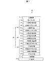
- FIG. 1 is a cross-sectional view showing the structure of a light-emitting element of this embodiment
- FIG. FIG. 4 is a cross-sectional view showing the light emitting state of the light emitting element of the present embodiment
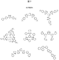
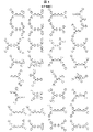
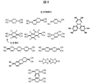
- It is an example of a material used for a light-emitting element. It is an example of a material used for a light-emitting element. It is an example of a material used for a light-emitting element. It is an example of a material used for a light-emitting element. It is an example of a material used for a light-emitting element. It is an example of a material used for a light-emitting element. It is an example of a material used for a light-emitting element.
- FIG. 9(a) and 9(b) are graphs showing the viewing angle-normalized luminance characteristics of the lower light emitting layer and the upper light emitting layer.
- FIG. 10(a) is a graph showing the viewing angle characteristics of the blue light emitting device of this embodiment
- FIG. 10(b) is a graph showing the viewing angle characteristics of the green light emitting device of this embodiment.
- (c) is a graph showing the viewing angle characteristics of the red light emitting device of this embodiment.
- 1 is a schematic cross-sectional view showing the configuration of a display device according to an embodiment
- FIG. 4 is a flow chart showing a method for manufacturing multi-color light-emitting elements in a display device.
- FIG. 1 is a cross-sectional view showing the configuration of the light emitting device of this embodiment.
- the light emitting device 80 includes a lower electrode 21, a hole injection layer 32, a lower hole transport layer 33, a lower electron blocking layer 34, a lower light emitting layer 35, a lower Side hole-blocking layer 36, lower electron-transporting layer 37, n-type charge-generating layer 41, p-type charge-generating layer 42, upper hole-transporting layer 53, upper electron-blocking layer 54, upper light-emitting layer 55, upper hole-blocking
- It is a top-emission type (structure for extracting light from above) that includes a layer 56, an upper electron-transporting layer 57, an electron-injecting layer 58, and an upper electrode 71 in this order.
- a hole-injecting layer 32 , a lower hole-transporting layer 33 , a lower electron-blocking layer 34 , a lower light-emitting layer 35 , a lower hole-blocking layer 36 , and a lower electron-transporting layer 37 constitute the first layer 30 .
- the upper hole-transporting layer 53, the upper electron-blocking layer 54, the upper light-emitting layer 55, the upper hole-blocking layer 56, the upper electron-transporting layer 57, and the electron-injecting layer 58 constitute the second layer 50
- the first layer 30 and the second layer 50 is disposed a charge generation layer 40 including an n-type charge generation layer (electron generation layer) 41 and a p-type charge generation layer (hole generation layer) 42 .
- the first layer 30 , the charge generating layer 40 and the second layer 50 make up the organic stack 60 .
- FIG. 2 is a cross-sectional view showing the light emitting state of the light emitting element of this embodiment.
- the lower electrode 21 functions as an anode and the upper electrode 71 functions as a cathode. Holes are supplied from the lower electrode 21 and electrons are supplied from the upper electrode 71.
- the charge generation layer 41 generates electrons and the p-type charge generation layer 42 generates holes. As a result, electrons and holes recombine in the lower light emitting layer 35 (excitons transition to the ground state), thereby emitting light in a predetermined wavelength range, and electrons and holes recombine in the upper light emitting layer 55. By combining, light in the predetermined wavelength range (light of the same color as that of the lower light emitting layer 35) is emitted.
- the electron transport material is not limited, for example, any one of electron transport organic materials such as oxadiazole compounds (eg, compound group A in FIG. 3 and compound group B in FIG. 4) can be used.
- a material obtained by adding Yb (ytterbium) or Li (lithium) in the range of 5 to 20% to the electron transporting organic material can be used.
- a material obtained by mixing an electron transporting organic material and Liq (lithium quinoline) at an appropriate ratio can be used.
- An electron-transporting organic material can be used as the hole blocking material for the lower hole blocking layer 36 and the upper hole blocking layer 56 .
- any one of the compound group C in FIG. 5 can be used.
- a material obtained by adding 1 to 10% of an electron accepting material to a hole transporting material can be used.
- any one of the compound group D in FIG. 6 can be used as the electron-accepting material, but the compound N (TCNQ-4F) is particularly suitable.
- the same material can be used for the p-type charge generation layer 42 and the hole injection layer 32 .
- Any one of the compound group E in FIG. 7, for example, can be used as the hole blocking material.
- the blue-emitting lower emitting layer 35 and upper emitting layer 55 may each include a host material (eg, compound 1 in FIG. 8) and a fluorescent dopant material (eg, compound 2 in FIG. 8).
- Each of the green-emitting lower emitting layer 35 and upper emitting layer 55 may comprise a host material (eg, compound 3 or compound 4 in FIG. 8) and a phosphorescent dopant material (eg, compound 5 in FIG. 8).
- Each of the red-emitting lower emitting layer 35 and upper emitting layer 55 may comprise a host material (eg, compound 6 of FIG. 8) and a phosphorescent dopant material (eg, compound 7 of FIG. 8).
- the lower electrode 21 (for example, the anode) can be configured by laminating ITO (Indium Tin Oxide) and Ag (silver) or an alloy containing Ag, for example.
- the upper electrode 71 (for example, cathode) can be made of a thin metal film such as a magnesium-silver alloy.
- the lower electrode 21 is light reflective
- the upper electrode 71 is light transmissive and light reflective
- the upper electrode 71 transmits more light than reflected light. Therefore, in the light-emitting element 80, by forming a macrocavity between the lower electrode 21 and the upper electrode 71, the light emitted from the front lower light-emitting layer 35 and the upper light-emitting layer 55 (having the same selected wavelength) can produce a resonance effect for This increases the intensity of the light of the selected wavelength, which can increase brightness and color purity.
- the lower electrode 21 and the lower electrode 21 are optimized (by approximating the resonance condition), the intensity becomes peaky near the selected wavelength of 625 [nm] for red light, near the selected wavelength of 535 [nm] for green light, and near the selected wavelength of 460 [nm] for blue light.
- Equation 1 For example, light with a wavelength ⁇ can obtain a resonance effect at the viewing angle ⁇ when Da satisfies Equation 1.
- m is an integer
- ⁇ a is the phase difference caused by light reflection at the lower electrode 21
- n is the refractive index of the organic laminate
- ⁇ e is the incident angle to the upper electrode 71 at the viewing angle ⁇ .
- the first viewing angle at which the resonance effect of the light of the selected wavelength emitted from the lower light emitting layer 35 is maximized, and the second viewing angle at which the resonance effect of the light of the selected wavelength emitted from the upper light emitting layer 55 is maximized It is different from the visual angle. That is, the first viewing angle is 0 degrees and the second viewing angle is an acute angle.
- Da is set so that the resonance effect is maximized at a vertical viewing angle
- Db is set so that the resonance effect is maximized at an oblique viewing angle
- do. DL is set to maximize the resonance effect at vertical viewing angles.
- LA in FIG. 9A is the normalized luminance of the lower light emitting layer 35 when Da is set so as to maximize the resonance effect at the vertical viewing angle (0 degrees), and LB in FIG.
- LT in FIG. It is the normalized luminance of the light emitting element. Comparing LT with LA in FIG. 5A, it can be seen that the luminance characteristics at viewing angles of 0 to 60 degrees are improved, and the color purity and viewing angle characteristics are enhanced.
- LA in FIG. 9B is the normalized luminance of the lower light emitting layer 35 when Da is set so as to maximize the resonance effect at the vertical viewing angle (0 degrees), and LB in FIG.
- LT in FIG. It is the normalized luminance of the light emitting element. Comparing LT with LA in FIG. 5B, it can be seen that the luminance at a viewing angle of 25 degrees or more is improved, but the luminance at a vertical viewing angle is low.
- Db is set to maximize the resonance effect at oblique viewing angles (10, 20, 25, 30, 40, 45, 50, and 60 degrees respectively). It is the normalized luminance of the element.
- Db (B3 to B5) so that the resonance effect is maximized at an oblique viewing angle of 20 degrees to 40 degrees for the blue light emitting element.
- Da is 116 [nm] to 126 [nm]
- Db is 192 [nm] to 212 [nm]
- DL is 220 [nm] to 240 [nm].
- FIG. 11 is a schematic cross-sectional view showing the configuration of the display device of this embodiment.
- a barrier layer 18, a TFT (thin film transistor) substrate 20 including pixel circuits, a blue light emitting element 80B, a green light emitting element 80G, and a red light emitting element 80R are provided on a substrate 15.
- An element layer 85, a sealing layer 87, and a functional layer 88 are provided in this order.
- the substrate 15 is a glass substrate or a flexible substrate whose main component is a resin such as polyimide.
- the substrate 15 can be composed of two layers of polyimide films and an inorganic film sandwiched between them.
- the barrier layer 18 can be composed of an inorganic insulating layer that prevents foreign substances such as water and oxygen from entering. Pixel circuits for controlling the blue light emitting element 80B, the green light emitting element 80G, and the red light emitting element 80R are formed in the TFT layer 20 .
- the light emitting element layer 85 includes a blue light emitting element 80B, a green light emitting element 80G, a red light emitting element 80R, and an insulating edge cover film 23 covering the edge of the lower electrode 21.
- the edge cover film 23 is formed, for example, by applying an organic material such as polyimide or acrylic resin and then patterning it by photolithography.
- the blue light emitting element 80B, green light emitting element 80G, and red light emitting element 80R are, for example, OLEDs (organic light emitting diodes).
- the sealing layer 87 that covers the light emitting element layer 85 is a layer that prevents foreign substances such as water and oxygen from penetrating into the light emitting element layer 85.
- the functional layer 88 is a layer having various functions such as optical control, touch sensor, and surface protection.
- the blue light emitting element 80B includes the lower electrode 21, the hole injection layer 32, the lower hole transport layer 33, the lower electron blocking layer 34, the lower light emitting layer 35B corresponding to the lower light emitting layer 35, and the lower light emitting layer 35B.
- the green light emitting element 80G includes the lower electrode 21, the hole injection layer 32, the lower hole transport layer 33, the lower electron blocking layer 34, the lower light emitting layer 35G corresponding to the lower light emitting layer 35, and the lower light emitting layer 35G.
- the red light emitting element 80R includes the lower electrode 21, the hole injection layer 32, the lower hole transport layer 33, the lower electron blocking layer 34, the lower light emitting layer 35R corresponding to the lower light emitting layer 35, and the lower light emitting layer 35R.
- 55R an upper hole blocking layer 56, an upper electron transport layer 57, an electron injection layer 58, and an upper electrode 71 in this order.
- the blue light emitting element 80B is designed, for example, as follows. That is, for the lower light emitting layer 35B, the distance Da1 from the lower electrode 21 is set so that the resonance effect is maximized at the vertical viewing angle, and for the upper light emitting layer 55B, the resonance effect is maximized at the oblique viewing angle. , and the distance DL1 between the lower electrode 21 and the upper electrode 71 is set so as to maximize the resonance effect at the vertical viewing angle.
- the design of the green light emitting element 80G is, for example, as follows. That is, for the lower light emitting layer 35G, the distance Da2 from the lower electrode 21 is set so that the resonance effect is maximized at the vertical viewing angle, and for the upper light emitting layer 55G, the resonance effect is maximized at the oblique viewing angle. , and the distance DL2 between the lower electrode 21 and the upper electrode 71 is set so as to maximize the resonance effect at the vertical viewing angle.
- the design of the red light emitting element 80R is, for example, as follows. That is, for the lower light emitting layer 35R, the distance Da3 from the lower electrode 21 is set so that the resonance effect is maximized at the vertical viewing angle, and for the upper light emitting layer 55R, the resonance effect is maximized at the oblique viewing angle. , and the distance DL3 between the lower electrode 21 and the upper electrode 71 is set so as to maximize the resonance effect at the vertical viewing angle. As a result, Da1 ⁇ Da2 ⁇ Da3, Db1 ⁇ Db2 ⁇ Db3, and DL1 ⁇ DL2 ⁇ DL3.
- each light emitting element can exhibit a microcavity effect (optical resonance effect), and color purity and viewing angle characteristics can be improved. It is possible to realize the display device 10 with high .
- FIG. 12 is a flow chart showing a method for manufacturing multi-color light-emitting elements in a display device.
- the lower electrode 21 is formed. Specifically, Ag and ITO are sequentially formed using a sputtering method.
- the hole injection layer 32 is formed. Specifically, co-evaporation of the hole-transporting material and the electron-accepting material is performed at a predetermined temperature and at a predetermined rate.
- the hole injection layer 32 is shared among the light emitting elements of a plurality of colors without using a fine metal mask.
- the lower hole transport layer 33 is formed. Specifically, the hole transport material is deposited at a predetermined temperature and at a predetermined rate. Here, a fine metal mask is not used, and the lower hole transport layer 33 is shared among the light emitting elements of a plurality of colors.
- step S4 the lower electron blocking layer 34 is formed. Specifically, the hole transport material is deposited at a predetermined temperature and at a predetermined rate. Here, a fine metal mask is used, and vapor deposition is performed so that the film thicknesses corresponding to the respective colors (blue light emitting element ⁇ green light emitting element ⁇ red light emitting element) are obtained.
- step S5 the lower light emitting layer 35 is formed. Specifically, co-evaporation of the light-emitting host and the dopant is performed at a predetermined temperature and at a predetermined rate.
- a fine metal mask is used to vapor-deposit materials corresponding to each color.
- the lower hole blocking layer 36 is formed. Specifically, the electron transport material is deposited at a predetermined temperature and at a predetermined rate. Here, a fine metal mask is not used, and the lower hole blocking layer 36 is shared among light emitting elements of a plurality of colors.
- the lower electron transport layer 37 is formed. Specifically, the electron transport material is deposited at a predetermined temperature and at a predetermined rate. Co-evaporation of an electron transporting material and lithium quinoline may also be used.
- a fine metal mask is not used, and the lower electron transport layer 37 is shared among light emitting elements of a plurality of colors.
- the n-type charge generation layer 41 is formed. Specifically, co-evaporation of the electron transport material and Yb or Li is performed at a predetermined temperature and at a predetermined rate. Here, a fine metal mask is not used, and the n-type charge generation layer 41 is shared among light emitting elements of a plurality of colors.
- the p-type charge generation layer 42 is formed. Specifically, co-evaporation of the hole-transporting material and the electron-accepting material is performed at a predetermined temperature and at a predetermined rate.
- the p-type charge generation layer 42 is shared among the light emitting elements of a plurality of colors without using a fine metal mask.
- the upper hole transport layer 53 is formed. Specifically, the hole transport material is deposited at a predetermined temperature and at a predetermined rate. Here, a fine metal mask is not used, and the upper hole transport layer 53 is shared among light emitting elements of a plurality of colors.
- the upper electron block layer 54 is formed. Specifically, the hole transport material is deposited at a predetermined temperature and at a predetermined rate. Here, a fine metal mask is used, and vapor deposition is performed so that the film thicknesses corresponding to the respective colors (blue light emitting element ⁇ green light emitting element ⁇ red light emitting element) are obtained.
- step S12 the upper light emitting layer 55 is formed. Specifically, co-evaporation of the light-emitting host and the dopant is performed at a predetermined temperature and at a predetermined rate.
- a fine metal mask is used to vapor-deposit materials corresponding to each color.
- step S13 the upper hole blocking layer 56 is formed. Specifically, the electron transport material is deposited at a predetermined temperature and at a predetermined rate. Here, a fine metal mask is not used, and the upper hole blocking layer 56 is shared among light emitting elements of a plurality of colors.
- the upper electron transport layer 57 is formed. Specifically, the electron transport material is deposited at a predetermined temperature and at a predetermined rate. Co-evaporation of an electron transporting material and lithium quinoline may also be used. Here, a fine metal mask is not used, and the upper electron transport layer 57 is shared between light emitting elements of a plurality of colors.
- step S15 the electron injection layer 58 is formed. Specifically, vapor deposition of lithium fluoride is performed at a predetermined temperature and at a predetermined rate. Here, a fine metal mask is not used, and the electron injection layer 58 is shared among light emitting elements of a plurality of colors.
- step S16 the upper electrode 71 is formed.
- a sputtering method is used to form, for example, a magnesium-silver alloy thin film.
- Light emission at a first viewing angle at which the resonance effect of the light of the selected wavelength emitted from the lower light emitting layer is maximized and a second viewing angle at which the resonance effect of the light of the selected wavelength emitted from the upper light emitting layer is maximized are different.
- Aspect 2 It is a top emission type that extracts light from the upper side, Aspect 1, for example, the light emitting device of Aspect 1, wherein the second viewing angle is an acute angle.
- the second viewing angle is an angle that forms 20 degrees or more and less than 45 degrees with respect to the normal to the upper light emitting layer.
- Aspect 6 comprising a plurality of charge functional layers between the lower electrode and the upper electrode;
- the light-emitting device eg, according to any one of aspects 1-5, wherein the plurality of charge functional layers includes a charge generating layer positioned between the lower light-emitting layer and the upper light-emitting layer.
- the charge generation layer comprises an electron generation layer and a hole generation layer;
- the organic laminate has a refractive index of 1.64 to 1.76.
- the light-emitting device for example, the light-emitting device according to aspect 5, wherein the thickness of the lower light-emitting layer is from 5 [nm] to 20 [nm], and the thickness of the upper light-emitting layer is from 15 [nm] to 40 [nm].
- the selected wavelength is 460 nm
- the distance between the lower electrode and the lower light emitting layer is 116 [nm] to 126 [nm]
- the distance between the lower electrode and the upper light emitting layer is 192 [nm] to 212 [nm]
- the light-emitting device according to aspect 10 wherein the organic laminate has a thickness of 220 [nm] to 240 [nm].
- the selected wavelength is 535 nm
- the distance between the lower electrode and the lower light-emitting layer is 134 [nm] to 144 [nm]
- the distance between the lower electrode and the upper light-emitting layer is 222 [nm] to 243 [nm]
- the light-emitting device according to aspect 10 wherein the organic laminate has a thickness of 255 [nm] to 275 [nm].
- the selected wavelength is 625 nm
- the distance between the lower electrode and the lower light-emitting layer is 158 [nm] to 168 [nm]
- the distance between the lower electrode and the upper light-emitting layer is 261 [nm] to 284 [nm]
- the light-emitting device according to aspect 10 wherein the organic laminate has a thickness of 298 [nm] to 318 [nm].
- the selected wavelength is 625 [nm], for example, the light emitting element according to Aspect 1 is included, and as a green light emitting element, the selected wavelength is 535 [nm], for example, the emission according to Aspect 1
- a display device comprising, as a blue light-emitting element, the light-emitting element according to aspect 1, for example, wherein the selected wavelength is 460 [nm].
- REFERENCE SIGNS LIST 10 display device 20 TFT substrate 21 lower electrode 35, 35B, 35G, 35R lower emitting layer 55, 55B, 55G, 55R upper emitting layer 60 organic laminate 71 upper electrode 80 light emitting element 85 light emitting element layer 87 sealing layer 88 Functional Layer 80R Red Light Emitting Element 80G Green Light Emitting Element 80B Blue Light Emitting Element
Landscapes
- Physics & Mathematics (AREA)
- Optics & Photonics (AREA)
- Electroluminescent Light Sources (AREA)
Priority Applications (3)
| Application Number | Priority Date | Filing Date | Title |
|---|---|---|---|
| US18/275,019 US12543475B2 (en) | 2021-02-08 | 2021-02-08 | Light-emitting element, display device |
| PCT/JP2021/004589 WO2022168312A1 (ja) | 2021-02-08 | 2021-02-08 | 発光素子、表示装置 |
| JP2022579298A JPWO2022168312A1 (https=) | 2021-02-08 | 2021-02-08 |
Applications Claiming Priority (1)
| Application Number | Priority Date | Filing Date | Title |
|---|---|---|---|
| PCT/JP2021/004589 WO2022168312A1 (ja) | 2021-02-08 | 2021-02-08 | 発光素子、表示装置 |
Publications (1)
| Publication Number | Publication Date |
|---|---|
| WO2022168312A1 true WO2022168312A1 (ja) | 2022-08-11 |
Family
ID=82742158
Family Applications (1)
| Application Number | Title | Priority Date | Filing Date |
|---|---|---|---|
| PCT/JP2021/004589 Ceased WO2022168312A1 (ja) | 2021-02-08 | 2021-02-08 | 発光素子、表示装置 |
Country Status (3)
| Country | Link |
|---|---|
| US (1) | US12543475B2 (https=) |
| JP (1) | JPWO2022168312A1 (https=) |
| WO (1) | WO2022168312A1 (https=) |
Cited By (2)
| Publication number | Priority date | Publication date | Assignee | Title |
|---|---|---|---|---|
| EP4404713A3 (en) * | 2023-01-17 | 2024-10-23 | Canon Kabushiki Kaisha | Light emitting element |
| JP2025081222A (ja) * | 2023-11-15 | 2025-05-27 | 安徽熙泰智能科技有限公司 | 高輝度oled表示デバイス、その其製造方法および表示装置 |
Citations (5)
| Publication number | Priority date | Publication date | Assignee | Title |
|---|---|---|---|---|
| JP2007265638A (ja) * | 2006-03-27 | 2007-10-11 | Sanyo Electric Co Ltd | 有機エレクトロルミネッセント素子 |
| US20150194471A1 (en) * | 2013-12-31 | 2015-07-09 | Lg Display Co., Ltd. | Organic light emitting display device and method for manufacturing the same |
| JP2016225221A (ja) * | 2015-06-02 | 2016-12-28 | コニカミノルタ株式会社 | 電界発光素子 |
| WO2017122386A1 (ja) * | 2016-01-14 | 2017-07-20 | コニカミノルタ株式会社 | 電界発光素子 |
| US20190198788A1 (en) * | 2017-11-30 | 2019-06-27 | Lg Display Co., Ltd. | Organic Light-Emitting Device and Organic Light-Emitting Display Device Using the Same |
Family Cites Families (6)
| Publication number | Priority date | Publication date | Assignee | Title |
|---|---|---|---|---|
| TW200714131A (en) | 2005-07-29 | 2007-04-01 | Sanyo Electric Co | Organic electroluminescent element and organic electroluminescent display device |
| JP2012195054A (ja) | 2011-03-14 | 2012-10-11 | Idemitsu Kosan Co Ltd | 有機エレクトロルミネッセンス素子 |
| US9112174B2 (en) * | 2011-08-12 | 2015-08-18 | Panasonic Corporation | Organic electroluminescent element |
| KR102567320B1 (ko) * | 2016-04-30 | 2023-08-16 | 엘지디스플레이 주식회사 | 유기 발광 소자 및 이를 적용한 유기 발광 표시 장치 |
| CN109659443B (zh) * | 2017-10-10 | 2024-03-22 | 京东方科技集团股份有限公司 | 显示面板、显示装置和改善显示面板色偏的方法 |
| CN117460288A (zh) * | 2023-10-17 | 2024-01-26 | 京东方科技集团股份有限公司 | 有机电致发光器件、显示面板和显示装置 |
-
2021
- 2021-02-08 WO PCT/JP2021/004589 patent/WO2022168312A1/ja not_active Ceased
- 2021-02-08 US US18/275,019 patent/US12543475B2/en active Active
- 2021-02-08 JP JP2022579298A patent/JPWO2022168312A1/ja active Pending
Patent Citations (5)
| Publication number | Priority date | Publication date | Assignee | Title |
|---|---|---|---|---|
| JP2007265638A (ja) * | 2006-03-27 | 2007-10-11 | Sanyo Electric Co Ltd | 有機エレクトロルミネッセント素子 |
| US20150194471A1 (en) * | 2013-12-31 | 2015-07-09 | Lg Display Co., Ltd. | Organic light emitting display device and method for manufacturing the same |
| JP2016225221A (ja) * | 2015-06-02 | 2016-12-28 | コニカミノルタ株式会社 | 電界発光素子 |
| WO2017122386A1 (ja) * | 2016-01-14 | 2017-07-20 | コニカミノルタ株式会社 | 電界発光素子 |
| US20190198788A1 (en) * | 2017-11-30 | 2019-06-27 | Lg Display Co., Ltd. | Organic Light-Emitting Device and Organic Light-Emitting Display Device Using the Same |
Cited By (3)
| Publication number | Priority date | Publication date | Assignee | Title |
|---|---|---|---|---|
| EP4404713A3 (en) * | 2023-01-17 | 2024-10-23 | Canon Kabushiki Kaisha | Light emitting element |
| JP2025081222A (ja) * | 2023-11-15 | 2025-05-27 | 安徽熙泰智能科技有限公司 | 高輝度oled表示デバイス、その其製造方法および表示装置 |
| JP7838847B2 (ja) | 2023-11-15 | 2026-04-01 | 安徽熙泰智能科技有限公司 | 高輝度oled表示デバイス、その其製造方法および表示装置 |
Also Published As
| Publication number | Publication date |
|---|---|
| US20240114715A1 (en) | 2024-04-04 |
| US12543475B2 (en) | 2026-02-03 |
| JPWO2022168312A1 (https=) | 2022-08-11 |
Similar Documents
| Publication | Publication Date | Title |
|---|---|---|
| US20250280712A1 (en) | Organic light-emitting diode display device including a thin film encapsulation layer | |
| CN100482025C (zh) | 有机电致发光显示器及其制造方法 | |
| TWI540938B (zh) | 有機發光元件的顯示器及其製造方法 | |
| CN101661951B (zh) | 彩色显示装置及其制造方法 | |
| US9018834B2 (en) | Organic light emitting device | |
| CN103915577B (zh) | 有机发光显示器件及其制造方法 | |
| TWI448194B (zh) | 有機發光元件,含彼之顯示元件,及含彼之照明裝置 | |
| US9859340B2 (en) | Organic electroluminescent display device having bent type or curved surface type display | |
| CN108029162B (zh) | 有机电致发光装置、照明装置和显示装置 | |
| US9343510B2 (en) | Organic light emitting display device | |
| US10217969B2 (en) | Organic light emitting diode display and method for fabricating the same | |
| US9949336B2 (en) | Organic light emitting diode device having electrode with Ag—Mg alloy | |
| Knauer et al. | Stacked inverted top-emitting green electrophosphorescent organic light-emitting diodes on glass and flexible glass substrates | |
| US20100283385A1 (en) | Organic el device | |
| JP2010080423A (ja) | カラー表示装置及びその製造方法 | |
| US20100327304A1 (en) | Organic el device and design method thereof | |
| JP2010056016A (ja) | カラー表示装置及びその製造方法 | |
| JP5832809B2 (ja) | 有機発光素子 | |
| CN108134012B (zh) | 有机发光二极管、有机发光显示面板及显示装置 | |
| JP4431125B2 (ja) | 平板ディスプレイ装置及びその製造方法 | |
| JP2019079699A (ja) | 表示装置 | |
| JP2012054091A (ja) | 多色表示装置 | |
| WO2022168312A1 (ja) | 発光素子、表示装置 | |
| Gaur et al. | Color Tunable Three Terminal (3‐T) Vertically Stacked Tandem Organic Electroluminescent Devices | |
| JP2018190666A (ja) | 有機エレクトロルミネッセンス素子、表示装置、照明装置 |
Legal Events
| Date | Code | Title | Description |
|---|---|---|---|
| 121 | Ep: the epo has been informed by wipo that ep was designated in this application |
Ref document number: 21924702 Country of ref document: EP Kind code of ref document: A1 |
|
| ENP | Entry into the national phase |
Ref document number: 2022579298 Country of ref document: JP Kind code of ref document: A |
|
| WWE | Wipo information: entry into national phase |
Ref document number: 18275019 Country of ref document: US |
|
| NENP | Non-entry into the national phase |
Ref country code: DE |
|
| 122 | Ep: pct application non-entry in european phase |
Ref document number: 21924702 Country of ref document: EP Kind code of ref document: A1 |
|
| WWG | Wipo information: grant in national office |
Ref document number: 18275019 Country of ref document: US |