WO2022157822A1 - Pixel circuit, display device, and method for driving same - Google Patents
Pixel circuit, display device, and method for driving same Download PDFInfo
- Publication number
- WO2022157822A1 WO2022157822A1 PCT/JP2021/001628 JP2021001628W WO2022157822A1 WO 2022157822 A1 WO2022157822 A1 WO 2022157822A1 JP 2021001628 W JP2021001628 W JP 2021001628W WO 2022157822 A1 WO2022157822 A1 WO 2022157822A1
- Authority
- WO
- WIPO (PCT)
- Prior art keywords
- bias
- switching element
- voltage
- data
- holding capacitor
- Prior art date
Links
- 238000000034 method Methods 0.000 title claims description 16
- 239000003990 capacitor Substances 0.000 claims abstract description 176
- 239000010409 thin film Substances 0.000 claims description 12
- 230000000415 inactivating effect Effects 0.000 claims description 6
- 239000004065 semiconductor Substances 0.000 claims description 5
- 229910021420 polycrystalline silicon Inorganic materials 0.000 claims description 4
- 229920005591 polysilicon Polymers 0.000 claims description 4
- 230000014759 maintenance of location Effects 0.000 claims description 2
- 238000005401 electroluminescence Methods 0.000 description 38
- 230000000052 comparative effect Effects 0.000 description 35
- 238000010586 diagram Methods 0.000 description 27
- 101100449067 Neurospora crassa (strain ATCC 24698 / 74-OR23-1A / CBS 708.71 / DSM 1257 / FGSC 987) cbs-2 gene Proteins 0.000 description 16
- 101100099821 Neurospora crassa (strain ATCC 24698 / 74-OR23-1A / CBS 708.71 / DSM 1257 / FGSC 987) cbs-1 gene Proteins 0.000 description 14
- 241000750042 Vini Species 0.000 description 13
- 230000008859 change Effects 0.000 description 10
- 230000004048 modification Effects 0.000 description 10
- 238000012986 modification Methods 0.000 description 10
- 101710171221 30S ribosomal protein S11 Proteins 0.000 description 5
- 101710171225 30S ribosomal protein S18 Proteins 0.000 description 5
- 230000000694 effects Effects 0.000 description 5
- 230000000630 rising effect Effects 0.000 description 4
- XLOMVQKBTHCTTD-UHFFFAOYSA-N Zinc monoxide Chemical compound [Zn]=O XLOMVQKBTHCTTD-UHFFFAOYSA-N 0.000 description 2
- 230000003071 parasitic effect Effects 0.000 description 2
- 230000000737 periodic effect Effects 0.000 description 2
- 239000002096 quantum dot Substances 0.000 description 2
- 230000009467 reduction Effects 0.000 description 2
- 101000641216 Aquareovirus G (isolate American grass carp/USA/PB01-155/-) Non-structural protein 4 Proteins 0.000 description 1
- GYHNNYVSQQEPJS-UHFFFAOYSA-N Gallium Chemical compound [Ga] GYHNNYVSQQEPJS-UHFFFAOYSA-N 0.000 description 1
- 101000927946 Homo sapiens LisH domain-containing protein ARMC9 Proteins 0.000 description 1
- 102100036882 LisH domain-containing protein ARMC9 Human genes 0.000 description 1
- 230000005540 biological transmission Effects 0.000 description 1
- 230000008094 contradictory effect Effects 0.000 description 1
- 238000013500 data storage Methods 0.000 description 1
- 230000001419 dependent effect Effects 0.000 description 1
- 230000006866 deterioration Effects 0.000 description 1
- 229910052733 gallium Inorganic materials 0.000 description 1
- 229910052738 indium Inorganic materials 0.000 description 1
- APFVFJFRJDLVQX-UHFFFAOYSA-N indium atom Chemical compound [In] APFVFJFRJDLVQX-UHFFFAOYSA-N 0.000 description 1
- 239000011159 matrix material Substances 0.000 description 1
- 230000007246 mechanism Effects 0.000 description 1
- 239000011787 zinc oxide Substances 0.000 description 1
Images


Classifications
-
- G—PHYSICS
- G09—EDUCATION; CRYPTOGRAPHY; DISPLAY; ADVERTISING; SEALS
- G09G—ARRANGEMENTS OR CIRCUITS FOR CONTROL OF INDICATING DEVICES USING STATIC MEANS TO PRESENT VARIABLE INFORMATION
- G09G3/00—Control arrangements or circuits, of interest only in connection with visual indicators other than cathode-ray tubes
- G09G3/20—Control arrangements or circuits, of interest only in connection with visual indicators other than cathode-ray tubes for presentation of an assembly of a number of characters, e.g. a page, by composing the assembly by combination of individual elements arranged in a matrix no fixed position being assigned to or needed to be assigned to the individual characters or partial characters
- G09G3/22—Control arrangements or circuits, of interest only in connection with visual indicators other than cathode-ray tubes for presentation of an assembly of a number of characters, e.g. a page, by composing the assembly by combination of individual elements arranged in a matrix no fixed position being assigned to or needed to be assigned to the individual characters or partial characters using controlled light sources
- G09G3/30—Control arrangements or circuits, of interest only in connection with visual indicators other than cathode-ray tubes for presentation of an assembly of a number of characters, e.g. a page, by composing the assembly by combination of individual elements arranged in a matrix no fixed position being assigned to or needed to be assigned to the individual characters or partial characters using controlled light sources using electroluminescent panels
- G09G3/32—Control arrangements or circuits, of interest only in connection with visual indicators other than cathode-ray tubes for presentation of an assembly of a number of characters, e.g. a page, by composing the assembly by combination of individual elements arranged in a matrix no fixed position being assigned to or needed to be assigned to the individual characters or partial characters using controlled light sources using electroluminescent panels semiconductive, e.g. using light-emitting diodes [LED]
- G09G3/3208—Control arrangements or circuits, of interest only in connection with visual indicators other than cathode-ray tubes for presentation of an assembly of a number of characters, e.g. a page, by composing the assembly by combination of individual elements arranged in a matrix no fixed position being assigned to or needed to be assigned to the individual characters or partial characters using controlled light sources using electroluminescent panels semiconductive, e.g. using light-emitting diodes [LED] organic, e.g. using organic light-emitting diodes [OLED]
- G09G3/3225—Control arrangements or circuits, of interest only in connection with visual indicators other than cathode-ray tubes for presentation of an assembly of a number of characters, e.g. a page, by composing the assembly by combination of individual elements arranged in a matrix no fixed position being assigned to or needed to be assigned to the individual characters or partial characters using controlled light sources using electroluminescent panels semiconductive, e.g. using light-emitting diodes [LED] organic, e.g. using organic light-emitting diodes [OLED] using an active matrix
- G09G3/3233—Control arrangements or circuits, of interest only in connection with visual indicators other than cathode-ray tubes for presentation of an assembly of a number of characters, e.g. a page, by composing the assembly by combination of individual elements arranged in a matrix no fixed position being assigned to or needed to be assigned to the individual characters or partial characters using controlled light sources using electroluminescent panels semiconductive, e.g. using light-emitting diodes [LED] organic, e.g. using organic light-emitting diodes [OLED] using an active matrix with pixel circuitry controlling the current through the light-emitting element
Definitions
- the present disclosure relates to a current-driven display device having a display element driven by current, such as an organic EL (Electro Luminescence) element, and particularly to a pixel circuit used in the display device.
- a display element driven by current such as an organic EL (Electro Luminescence) element
- a pixel circuit of an organic EL display device includes a drive transistor, a write control transistor, a holding capacitor, etc. in addition to the organic EL element.
- a thin film transistor is used for the drive transistor and the write control transistor, and a holding capacitor is connected to the gate terminal as the control terminal of the drive transistor.
- a voltage corresponding to a video signal representing an image to be displayed (more specifically, a voltage representing a gradation value of a pixel to be formed by the pixel circuit) is applied as a data voltage.
- An organic EL element is a self-luminous display element that emits light with a luminance corresponding to the current flowing through it.
- the drive transistor is provided in series with the organic EL element and controls the current flowing through the organic EL element according to the voltage held in the holding capacitor.
- a display device that performs pause driving is known as a display device with low power consumption.
- pause driving when the same image is displayed continuously, a drive period (refresh period) and a rest period (non-refresh period) are provided, the drive circuit is operated during the drive period, and the operation of the drive circuit is stopped during the rest period.
- It is a driving method, and is also called “intermittent driving” or "low frequency driving”.
- Pause driving can be applied when the off-leakage current of a transistor as a switching element included in a pixel circuit is small.
- a thin film transistor hereinafter referred to as an "oxide TFT" having a channel layer formed of an oxide semiconductor is known.
- indium gallium zinc oxide (InGaZnO) is used as the oxide semiconductor.
- the adopted oxide TFT (hereinafter referred to as “IGZO-TFT”) is used.
- IGZO-TFT thin film transistor
- LTPS-TFT thin film transistor having a channel layer formed of low-temperature polysilicon with high mobility
- IGZO-TFT having a small off-leak current is used as a switching element.
- An organic EL display device has been proposed in which a display unit configured by such a pixel circuit is used as a pixel circuit and performs pause driving (see, for example, US Patent Application Publication No. 2020/0118487).
- the organic EL element of each pixel circuit When rest driving is performed in an organic EL display device, the organic EL element of each pixel circuit is turned off by the light emission control transistor during a non-light emitting period provided for each frame period in the driving period. The operation of the circuit stops, and the organic EL element of each pixel circuit continues to emit light with a luminance corresponding to the data voltage written in the previous driving period.
- the pause period is much longer than the drive period (for example, the drive period consists of one or several frame periods, and the pause period consists of several tens of frame periods). , such drive periods and rest periods alternate. Therefore, when such a pause drive is performed, the off-lighting of the organic EL element during the drive period is visually recognized as flicker.
- the thin film transistor as the driving transistor in the pixel circuit has hysteresis. Due to its characteristic, flicker is still visible in low frequency drive (pause drive). That is, in this periodic light-off configuration, the voltage stress applied to the thin film transistor as the drive transistor differs between the drive period and the rest period. Unlike, this makes the flicker visible.
- bias stress voltage hereinafter referred to as "on-bias voltage” or simply “bias voltage”
- bias voltage is applied intentionally to the drive transistor during the idle period.
- a current-driven display device such as an organic EL display device be able to perform good display without visible flicker in the entire area of the display image even if the pause drive is performed.
- a pixel circuit is a display device having a display section including a plurality of data signal lines, a plurality of first scanning signal lines, a plurality of emission control lines, and first and second power supply lines. in any one of the plurality of data signal lines, corresponding to any one of the plurality of first scanning signal lines, and any one of the plurality of emission control lines
- a correspondingly arranged pixel circuit comprising: a display element driven by a current; a drive transistor having a control terminal, a first conduction terminal, and a second conduction terminal and provided in series with the display element; a data retention capacitor; a data write control switching element having a control terminal connected to a corresponding first scanning signal line and controlling writing of the voltage of the corresponding data signal line to the data holding capacitor; a first emission control switching element having a control terminal connected to a corresponding emission control line; a bias supply circuit;
- the display unit further includes a plurality of bias control lines, the pixel circuit corresponds to one of the plurality of
- a display device comprises: a display unit including a plurality of data signal lines, a plurality of first scanning signal lines, a plurality of emission control lines, a plurality of bias control lines, a first power supply line, a second power supply line, and a plurality of pixel circuits; a data side driver circuit that generates a plurality of data signals and applies them to the plurality of data signal lines; a scanning side drive circuit that selectively drives the plurality of first scanning signal lines, selectively drives the plurality of emission control lines, and selectively drives the plurality of bias control lines; A driving period consisting of a refresh frame period for writing the voltages of the plurality of data signals to the plurality of pixel circuits as data voltages, and a rest period consisting of a non-refresh frame period for stopping writing of the data voltages to the plurality of pixel circuits.
- each of the plurality of pixel circuits corresponds to any one of the plurality of data signal lines, corresponds to any one of the plurality of first scanning signal lines, and corresponds to any one of the plurality of emission control lines; , and corresponding to any one of the plurality of bias control lines, a display element driven by current; a drive transistor having a control terminal, a first conduction terminal and a second conduction terminal and provided in series with the display element; a data holding capacitor; and a corresponding first scanning signal line.
- a data write control switching element for controlling writing of the voltage of the corresponding data signal line to the data holding capacitor and having a control terminal connected to the corresponding light emission control line; including a light emission control switching element and a bias supply circuit,
- the bias supply circuit has a bias holding capacitor for holding a voltage corresponding to the voltage of the corresponding data signal line, and a control terminal connected to the corresponding bias control line, and is connected in series with the bias holding capacitor.
- the display control circuit is In the drive period, the voltage of the corresponding data signal line is written and held as the data voltage in the data holding capacitor when the first light emission control switching element is in an off state, and a voltage corresponding to the data voltage is produced.
- the data-side driving circuit and the controlling the scanning side drive circuit In the idle period, when the first light emission control switching element is in an off state, the voltage held by the bias holding capacitor is applied to the first conduction terminal of the driving transistor through the bias control switching element.
- the scanning side drive circuit is controlled such that a current corresponding to the voltage held by the data holding capacitor flows through the display element when the light emission control switching element is in an ON state.
- a driving method provides a display including a plurality of data signal lines, a plurality of first scanning signal lines, a plurality of emission control lines, first and second power supply lines, and a plurality of pixel circuits.
- a method of driving a display device comprising: The display unit further includes a plurality of bias control lines, each of the plurality of pixel circuits, corresponds to any one of the plurality of data signal lines, corresponds to any one of the plurality of first scanning signal lines, and corresponds to any one of the plurality of emission control lines; , and corresponding to any one of the plurality of bias control lines, a display element driven by current; a drive transistor having a control terminal, a first conduction terminal and a second conduction terminal and provided in series with the display element; a data holding capacitor; and a corresponding first scanning signal line.
- a data write control switching element for controlling writing of the voltage of the corresponding data signal line to the data holding capacitor and having a control terminal connected to the corresponding light emission control line; including a light emission control switching element and a bias supply circuit,
- the bias supply circuit has a bias holding capacitor for holding a voltage corresponding to the voltage of the corresponding data signal line, and a control terminal connected to the corresponding bias control line, and is connected in series with the bias holding capacitor.
- the driving method includes a drive period consisting of a refresh frame period in which voltages of a plurality of data signals are written as data voltages in the plurality of pixel circuits, and a non-refresh frame period in which writing of data voltages to the plurality of pixel circuits is stopped.
- the rest drive step includes: In the drive period, when the first light emission control switching element is in an off state, the voltage of the corresponding data signal line is written and held in the data holding capacitor as a data voltage, and a voltage corresponding to the data voltage is produced. The plurality of data signals are written and held in the bias holding capacitor so that a current corresponding to the voltage held in the data holding capacitor flows through the display element when the first emission control switching element is in an ON state.
- the idle period when the first light emission control switching element is in an off state, the voltage held by the bias holding capacitor is applied to the first conduction terminal of the driving transistor through the bias control switching element, Driving of the plurality of first scanning signal lines is stopped so that a current corresponding to the voltage held by the data holding capacitor flows through the display element when the light emission control switching element is in an ON state, and the plurality of bias control lines are driven. and selectively inactivating the plurality of emission control lines.
- the bias holding capacitor In a display device using a pixel circuit including a bias supply circuit having a bias control switching element and a bias control switching element, when pause driving is performed in which a drive period consisting of a refresh frame period and a rest period consisting of a non-refresh frame period alternately appear, The emission control line and the bias control line are driven during both the drive period and the rest period.
- the bias holding capacitor By driving the light emission control line and the bias control line in this manner, in each pixel circuit, when the voltage of the data signal line is written into the data holding capacitor, the bias holding capacitor also responds to the voltage of the data signal line during the drive period. The voltage is written and held, and in the idle period, the holding voltage of the bias holding capacitor is applied to the first conduction terminal of the drive transistor during the non-light emitting period. That is, a bias stress voltage corresponding to the display gradation of the pixel circuit is applied to the first conduction terminal of the driving transistor during the non-light emitting period of the idle period.
- FIG. 1 is a block diagram showing the overall configuration of a display device according to a first embodiment
- FIG. 4 is a timing chart for explaining the schematic operation in the normal drive mode of the display device according to the first embodiment
- FIG. 4 is a circuit diagram showing a configuration of a pixel circuit in a comparative example with respect to the first embodiment
- 4 is a timing chart for explaining the operation of the pixel circuit in the comparative example
- 7A and 7B are circuit diagrams for explaining the initialization operation, the data write operation, and the lighting operation of the pixel circuit in the comparative example
- FIG. 10 is a circuit diagram for explaining a light-off operation (without on-bias application) and an on-bias application operation of the pixel circuit in the comparative example;
- 2 is a circuit diagram showing the configuration of a pixel circuit in the first embodiment;
- FIG. 4 is a timing chart for explaining the operation of the pixel circuit in the first embodiment;
- FIG. 4A and 4B are circuit diagrams for explaining an initialization operation, a data write operation, and a lighting operation of the pixel circuit in the first embodiment;
- FIG. 4A and 4B are circuit diagrams for explaining a light-off operation (without on-bias application) and an on-bias application operation of the pixel circuit in the first embodiment;
- FIG. 5 is a timing chart for explaining a method of driving the display device according to the comparative example; 4 is a timing chart for explaining a driving method of the display device according to the first embodiment;
- FIG. 5 is a waveform diagram for explaining the extinguishing operation in the first embodiment and the comparative example;
- FIG. 4 is a waveform diagram for explaining a difference in turn-off waveforms between the first embodiment and the comparative example;
- FIG. 7 is a circuit diagram showing the configuration of a pixel circuit in a display device according to a second embodiment; 8 is a timing chart for explaining the operation of the pixel circuit in the second embodiment;
- FIG. 8A and 8B are circuit diagrams for explaining an initialization operation, a data write operation, and a lighting operation of the pixel circuit in the second embodiment
- FIG. FIG. 10 is a circuit diagram for explaining the extinguishing operation (without on-bias application) and the on-bias application operation of the pixel circuit in the second embodiment
- FIG. 4 is a circuit diagram showing the configuration of a pixel circuit in a display device according to a modification of the first embodiment; 20 is a timing chart for explaining the operation of the pixel circuit shown in FIG. 19;
- FIG. 4 is a circuit diagram showing a configuration example when a bias supply circuit is provided in a pixel circuit that does not perform threshold compensation by diode connection; 22 is a timing chart for explaining the operation of the pixel circuit shown in FIG. 21;
- the gate terminal corresponds to the control terminal
- one of the drain terminal and the source terminal corresponds to the first conduction terminal
- the other corresponds to the second conduction terminal.
- connection in this specification means “electrical connection” unless otherwise specified. Indirect connection via an element is also included.
- FIG. 1 is a block diagram showing the overall configuration of a display device 10 according to the first embodiment.
- This display device 10 is an organic EL display device that performs internal compensation. That is, in the display device 10, each pixel circuit 15 has a function of compensating for variations and fluctuations in the threshold voltage of the driving transistor therein.
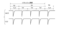
- the display device 10 also has two operation modes, a normal drive mode and a pause drive mode. That is, in the normal drive mode, the display device 10 operates so that the refresh frame periods Trf for rewriting the image data (data voltage in each pixel circuit) of the display section are continuous.
- a driving period TD and a rest period TP consisting of a plurality of non-refresh frame periods Tnrf for stopping rewriting of image data on the display section alternately appear (see FIG. 12 described later).
- the display device 10 includes a display section 11, a display control circuit 20, a data side drive circuit 30, a scanning side drive circuit 40, and a power supply circuit .
- the data side driver circuit 30 functions as a data signal line driver circuit (also called “data driver”).
- the scanning-side driving circuit 40 functions as a scanning signal line driving circuit (also called “gate driver”), a light emission control circuit (also called “emission driver”), and a bias control circuit.
- these three scanning-side circuits are implemented as one scanning-side drive circuit 40, but these three circuits may be separated as appropriate, and these three circuits may be separated. may be arranged separately on one side and the other side of the display section 11 .
- the power supply circuit 50 supplies the display unit 11 with a high-level power supply voltage ELVDD, a low-level power supply voltage ELVSS, an initialization voltage Vini, a display control circuit 20 , a data-side drive circuit 30 , and a scanning-side drive circuit 40 . and a power supply voltage (not shown) to be supplied to .
- the display unit 11 has m data signal lines D1, D2, .
- This (n is an integer equal to or greater than 2) second scanning signal lines NS-1, NS0, NS1, . . . , NSn are arranged.
- n light emission control lines (emission lines) EM1 to EMn are arranged along the n first scanning signal lines PS1 to PSn, respectively, and the n first scanning signal lines PS1 to PSn are provided with n light emission control lines (emission lines) EM1 to EMn, respectively.
- n bias control lines BS1 to BSn are arranged along it.
- the display unit 11 is provided with m ⁇ n pixel circuits 15 arranged in a matrix along m data signal lines D1 to Dm and n first scanning signal lines PS1 to PSn. .
- Each pixel circuit 15 corresponds to one of the m data signal lines D1 to Dm and corresponds to one of the n first scanning signal lines PS1 to PSn (hereinafter each pixel circuit 15 , the pixel circuit corresponding to the i-th first scanning signal line PSi and the j-th data signal line Dj is also referred to as the "i-th row j-th column pixel circuit", and the code "Pix (i, j )”).
- Each pixel circuit 15 corresponds to any one of the n second scanning signal lines NS1 to NSn and to any one of the n emission control lines EM1 to EMn. Each pixel circuit 15 also corresponds to any one of the n bias control lines BS1 to BSn.
- a power supply line (not shown) common to each pixel circuit 15 is arranged. That is, a first power supply line (hereinafter referred to as a “high level power supply line” and a symbol “ ELVDD”), and a second power supply line as a fixed voltage line for supplying the low level power supply voltage ELVSS for driving the organic EL element (hereinafter referred to as "low level power supply line", low level power supply voltage (indicated by the symbol "ELVSS”) is arranged.
- the display unit 11 is provided with an initialization voltage Vini as a fixed voltage line (not shown) for supplying an initialization voltage Vini used for a reset operation (also referred to as an “initialization operation”) for initializing each pixel circuit 15 .
- a line (labeled "Vini" like the initialization voltage) is also provided.
- a high-level power supply voltage ELVDD, a low-level power supply voltage ELVSS, and an initialization voltage Vini are supplied from the power supply circuit 50 .
- the display control circuit 20 receives an input signal Sin including image information representing an image to be displayed and timing control information for image display from the outside of the display device 10, and based on this input signal Sin, a data side control signal Scd and a scanning signal. A side control signal Scs is generated, and a data side control signal Scd and a scanning side control signal Scs are output to the data side driving circuit 30 and the scanning side driving circuit 40, respectively.
- the data side drive circuit 30 drives the data signal lines D1 to Dm based on the data side control signal Scd from the display control circuit 20. That is, the data-side drive circuit 30 generates m data signals D(1) to D(m) representing images to be displayed based on the data-side control signal Scd, and applies them to the data signal lines D1 to Dm, respectively. .
- the scanning drive circuit 40 drives the n first scanning signal lines PS1 to PSn and the n+2 second scanning signal lines NS-1 to NSn based on the scanning control signal Scs from the display control circuit 20. It functions as a signal line drive circuit, an emission control circuit that drives the emission control lines EM1 to EMn, and a bias control circuit that drives the bias control lines BS1 to BSn.
- the scanning-side driving circuit 40 drives the n first scanning signal lines PS1 to PSn for one horizontal period based on the scanning-side control signal Scs.
- n+2 second scanning signal lines NS-1 to NSn are sequentially selected for a predetermined period corresponding to one horizontal period, and the selected first scanning signal line PSk is activated for a predetermined period.
- a signal is applied (k is an integer satisfying 1 ⁇ k ⁇ n), an active signal is applied to the selected second scanning signal line NSs (s is an integer satisfying ⁇ 1 ⁇ s ⁇ n), and An inactive signal is applied to the selected first scanning signal line, and an inactive signal is applied to the non-selected second scanning signal line.
- m pixel circuits Pix(k, 1) to Pix(k, m) corresponding to the selected first scanning signal line PSk are collectively selected.
- m data signals D (1 ) to D(m) (hereinbelow, these voltages may be simply referred to as “data voltages” without distinction) are used as pixel data for the pixel circuits Pix(k, 1) to Pix(k, m ), respectively.
- a light-emission control signal high level
- a light emission control signal low level voltage
- the organic EL elements in the pixel circuits Pix (i, 1) to Pix (i, m) corresponding to the i-th first scanning signal line PSi are connected to the light emission control line. While the voltage of EMi is at the low level (activated state), the i-th pixel circuits Pix(i, 1) to Pix(i, m) emit light with luminance corresponding to the data voltages written respectively.
- the scanning-side drive circuit 40 also drives the emission control lines EM1 to EMn during the non-refresh frame period Tnrf in the same manner as during the refresh frame period Tnrf (see FIG. 12, which will be described later).
- the scanning-side drive circuit 40 drives the bias control lines BS1 to BSn so that they are sequentially selected in both the refresh frame period Trf and the non-refresh frame period Tnrf in the rest drive mode. (see FIG. 12 described later). Details of this operation will be described later.
- driving of the bias control lines BS1-BSn is stopped, and the bias control lines BS1-BSn are all maintained in a non-selected state.
- the display device 10 has two operation modes, the normal drive mode and the pause drive mode. First, the general operation of the display device 10 in the normal drive mode will be described.
- FIG. 2 is a timing chart for explaining the schematic operation of the display device 10 in normal drive mode.
- the scanning-side control signal Scs supplied from the display control circuit 20 to the scanning-side driving circuit 40 includes a two-phase clock signal composed of the first and second gate clock signals CK1 and CK2.
- the scan-side drive circuit 40 In the normal drive mode, the scan-side drive circuit 40 generates first scan signals PS(1) to PS(n) and second scan signals NS(-1), NS as shown in FIG. 2 based on the two-phase clock signals. (0), NS(1), . NS(-1) to NS(n) are applied to the second scanning signal lines NS-1 to NSn, respectively. Further, the scanning-side drive circuit 40 generates emission control signals EM(1) to EM(n) as shown in FIG.
- the data-side drive circuit 30 Based on the data-side control signal Scd from the display control circuit 20, the data-side drive circuit 30 outputs a data signal that changes in conjunction with the first scanning signals PS(1) to PS(n) as shown in FIG. D(1) to D(m) are generated and applied to the data signal lines D1 to Dm, respectively.
- each pixel circuit Pix(i, j) is initialized and data voltage is written. to emit light.
- the above various signals shown in FIG. By being driven as described above, the first scanning signal lines PS1 to PSn and the second scanning signal lines NS-1 to NSn are sequentially selected in one frame period, and the pixel circuits Pix (1, 1 of the display section 11) are selected. ) to Pix(n,m)) are repeated.
- the bias control lines BS1 to BSn are stopped from being driven and are maintained in a non-selected state (low level voltage).
- a drive period TD consisting of such a refresh frame period (hereinafter also referred to as "RF frame period”) Trf and a plurality of non-refresh frame periods (
- a pause period TP consisting of Tnrf (hereinafter also referred to as an "NRF frame” period) is alternately repeated.
- the scanning side driving circuit 40 drives the first scanning signal lines PS1 to PSn and the second scanning signal lines NS-1 to NSn, and the data side driving circuit 30 drives the data signal lines D1 to
- the driving of Dm is stopped, and the display based on the image data written in the previous driving period TD (RF frame period Trf) continues. Therefore, the rest drive mode is effective in reducing the power consumption of the display device when displaying a still image.
- bias control lines BS1-BSn are driven so as to be sequentially selected in both RF frame period Trf and NRF frame period Tnrf in the rest drive mode.
- the driving period TD is composed of only one RF frame period Trf, but may be composed of two or more RF frame periods Trf.
- the input signal Sin from the outside includes an operation mode signal Sm that indicates in which operation mode the display unit 11 is to be driven, the normal drive mode or the rest drive mode.
- This operation mode signal Sm is applied to the scanning side driving circuit 40 as part of the scanning side control signal Scs, and is also applied to the data side driving circuit 30 as part of the data side control signal Scd.
- the scanning-side drive circuit 40 drives the first scanning signal lines PS1 to PSn and the second scanning signal lines NS-1 to NSn according to the operation mode indicated by the operation mode signal Sm, and drives the emission control lines EM1 to EMn. They are driven in the same manner (same cycle and same duty ratio) regardless of whether they are in the normal drive mode or the rest drive mode.
- the scanning-side drive circuit 40 drives the bias control lines BS1 to BSn in the pause drive mode, and stops driving them in the normal drive mode.
- the data side drive circuit 30 drives the data signal lines D1 to Dn according to the operation mode indicated by this operation mode signal Sm. Since the subject of the present application is not related to the normal drive mode, the operation of the display device 10 or its pixel circuit will be mainly described below in the rest drive mode (the same applies to other embodiments described later). ).
- each pixel circuit Pix(i, j) data is written when the corresponding first and second scanning signal lines PSi, NSi are in the selected state.
- An initializing operation is performed when the second scanning signal line NSi-2 two lines before the second scanning signal line NSi is in a selected state.
- P-channel transistors are used as the first and second emission control transistors T5 and T6.
- L level voltage of level
- H level voltage of high level
- pixel circuit in the comparative example a pixel circuit in a display device as a comparative example of the present embodiment
- the configuration and operation of the pixel circuit 15 in the present embodiment The operation will be described in comparison with the configuration and operation of the pixel circuit in the comparative example.
- the bias control lines BS1 to BSn are not provided in the display section of the display device as the comparative example, and therefore the scanning side drive circuit 40 does not have a function as a bias control circuit.
- the configuration of the display device as the comparative example is the same as that of the display device according to the present embodiment except for the components related to the bias control lines BS1 to BSn. , and the description is omitted.
- a pixel circuit corresponding to such a configuration will be described as a pixel circuit in a comparative example.
- the inventor of the present application has confirmed that even if such a configuration is adopted, flicker cannot necessarily be suppressed in the entire area of the display image, and flicker can still be visually recognized. Therefore, hereinafter, the configuration and operation of the pixel circuit in the comparative example will be described while referring to the mechanism that causes this problem.
- the transistors T1, T2, and T7 are N-type transistors (more specifically, N-type IGZO-TFTs).
- the transistors T3 to T6 are P-type transistors (more specifically, P-type LTPS-TFTs).
- the data holding capacitor Cst is a capacitive element having two electrodes consisting of a first electrode and a second electrode. In the pixel circuit 15, the transistors T1 to T3 and T5 to T7 other than the driving transistor T4 function as switching elements.
- a corresponding first scanning signal line hereinafter also referred to as a "corresponding first scanning signal line” in the description focused on the pixel circuit) PSi, and a corresponding second scanning signal line.
- corresponding second scanning signal line in the description focused on the pixel circuit
- the second scanning signal line two lines before the corresponding second scanning signal line NSi second scanning signal lines NS-1 to the scanning signal line two lines before NSn in the scanning order
- the i-2-th second scanning signal line hereinafter also referred to simply as the "preceding second scanning signal line” in the description focused on the pixel circuit) NSi-2
- Corresponding light emission control line hereinafter also referred to as “corresponding light emission control line” in the description focusing on the pixel circuit) EMi
- corresponding data signal line hereinafter also referred to as "corresponding data signal line” in the description focusing on the pixel circuit
- the gate terminal as the control terminal of the driving transistor T4 is connected to the high-level power supply line ELVDD via the data holding capacitor Cst. It is connected to the initialization voltage line Vini through the first initialization transistor T1.
- a source terminal as a first conductive terminal of the drive transistor T4 is connected to the high-level power supply line ELVDD through the first light emission control transistor T5, and is connected to the corresponding data signal line Dj through the data write control transistor T3.
- a drain terminal as a second conductive terminal of the driving transistor T4 is connected to an anode electrode as a first terminal of the organic EL element OL via the second emission control transistor T6, and is connected to the driving transistor T4 via the threshold compensating transistor T2. It is connected to the gate terminal of transistor T4.
- the anode electrode of the organic EL element OL is connected to the initialization voltage line Vini through the second initialization transistor T7, and the cathode electrode as the second terminal of the organic EL element OL is connected to the low level power supply line ELVSS.
- the gate terminal of the data write control transistor T3 is connected to the first scanning signal line PSi
- the gate terminal of the threshold compensating transistor T2 is connected to the second scanning signal line NSi
- the gate terminal of the first initialization transistor T1 is connected to the preceding second scanning signal line. NSi-2, respectively.
- Gate terminals of the first emission control transistor T5, the second emission control transistor T5, and the second initialization transistor T7 are all connected to the corresponding emission control line EMi.
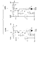
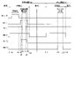
- FIG. 4 is a timing chart for explaining the operation of the pixel circuit Pix(i,j) during the non-light emitting period included in each frame period.
- times t1 to t8 are included in the RF frame period Trf that constitutes the drive period TD
- the drive period TD is switched to the pause period TP at time t9
- times t10 to t12 are the first frames in the pause period TP. It is included in the NRF frame period Tnrf.
- a light emission control signal (hereinafter referred to as a “corresponding light emission control signal”) EM(i) supplied to the pixel circuit Pix(i,j) of FIG. 3 via a corresponding light emission control line EMi changes from L level to H level at time t1.
- the P-type first and second emission control transistors T5 and T6 change from the ON state to the OFF state, and maintain the OFF state while the emission control signal EM(i) is at H level. Therefore, during the period t1 to t8 when the light emission control signal EM(i) is at H level, no current flows through the organic EL element OL and the pixel circuit Pix(i,j) is in the off state.
- the N-type second initialization transistor T7 is turned on, thereby initializing the voltage Va of the anode electrode of the organic EL element OL (hereinafter referred to as "anode voltage").
- anode voltage Such initialization of the anode voltage Va cuts off the influence of the past display history and suppresses deterioration of the display quality.
- the light emission control signal EM(i) supplied to the gate terminal of the second initialization transistor T7 is driven in the idle period TP in the same manner as in the drive period TD (see FIG. 4). Therefore, the initialization of the anode voltage Va by the second initialization transistor T7 works in the direction of further suppressing flicker in the pause drive by making the extinguishing period the same length in the drive period TD and the pause period TP.
- the second scanning signal supplied to the pixel circuit Pix(i, j) through the preceding second scanning signal line NSi-2 during the period in which the pixel circuit Pix(i, j) is in the off state that is, the non-light emitting period t1 to t8.
- NS(i-2) (hereinafter also referred to as "preceding second scanning signal”) changes from L level to H level at time t2.
- the N-type first initialization transistor T1 changes from the off state to the on state, and maintains the on state while the second scanning signal NS(i-2) is at H level.
- the data holding capacitor Cst is initialized, and the gate terminal of the driving transistor T4 and the first electrode of the data holding capacitor Cst are initialized. and the voltage of the node N2 becomes the initialization voltage Vini. That is, the voltage Vg of the gate terminal of the drive transistor T4 (hereinafter referred to as "gate voltage”) becomes the initialization voltage Vini.
- the pixel circuit 15a schematically shows the state of the pixel circuit Pix(i, j) at this time, that is, the circuit state during the initialization operation.
- dotted line circles indicate that the transistors as switching elements therein are in the OFF state
- dotted line rectangles indicate that the transistors as switching elements therein are in the ON state. It shows that Such a representation method is also employed in the pixel circuits 15a (WR) and 15a (EM) in FIG. 5, and further employed in FIGS. It is
- a second scanning signal (hereinafter also referred to as a "corresponding second scanning signal”) NS(i) given by the second scanning signal NS(i) changes from L level to H level at time t4.
- the N-type threshold compensating transistor T2 changes from an off state to an on state, and maintains the on state while the corresponding second scanning signal NS(i) is at H level. and its drain terminal are short-circuited, that is, in a diode-connected state.
- the first scanning signal (hereinafter also referred to as the “corresponding first scanning signal”) is applied to the pixel circuit Pix(i,j) through the corresponding first scanning signal line PSi. ) PS(i) changes from H level to L level at time t5. As a result, the P-type data write control transistor T3 changes from the off state to the on state, and maintains the on state while the corresponding first scanning signal PS(i) is at L level.
- a data signal D ( The voltage j) is applied as the data voltage Vdata to the data holding capacitor Cst via the diode-connected drive transistor T4.
- the threshold-compensated data voltage is written to and held in the data holding capacitor Cst, and the gate voltage Vg of the driving transistor T4 becomes the voltage of the first electrode of the data holding capacitor Cst (hereinafter referred to as the voltage of the data holding capacitor Cst). (also called “holding voltage”).
- the pixel circuit 15a (WR) schematically shows the state of the pixel circuit Pix(i, j) at this time, that is, the circuit state during the data write operation.
- the corresponding second scanning signal NS(i) changes from H level to L level, and the threshold compensation transistor T2 is turned off.
- the corresponding light emission control signal EM(i) changes from H level to L level, thereby turning on the first and second light emission control transistors T5 and T6, and the light emission period starts.
- It flows through the control transistor T5, the drive transistor T4, the second emission control transistor T6, and the organic EL element OL to the low-level power supply line ELVSS.
- the organic EL element OL emits light with luminance corresponding to the current I1.
- the pixel circuit 15a schematically shows the state of the pixel circuit Pix(i, j) at this time, that is, the circuit state during the lighting operation.
- the above light emission period continues until time t9 when the corresponding light emission control signal EM(i) changes from L level to H level.
- the corresponding emission control signal EM(i) changes to H level at time t9
- the first and second emission control transistors T5 and T6 change from ON to OFF
- the emission control signal EM(i) changes to H level. remains off during Therefore, during the period t9 to t12 in which the light emission control signal EM(i) is at H level, no current flows through the organic EL element OL, and the pixel circuit Pix(i,j) is in the off state.
- the drive period TD is switched to the pause period TP.
- the driving of the second scanning signal lines NS-1 to NSn is stopped and the second scanning signals NS(-1) to NS(n) are maintained at L level.
- the driving of the single scanning signal lines PS1 to PSn and the emission control lines EM1 to EMn continues (see FIG. 4 and FIG. 11 described later).
- the corresponding first scanning signal PS(i) changes from the H level to the L level at time t10 during the non-light emitting period t9 to t12 within the pause period TP (NRF frame period Tnrf).
- the data write control transistor T3 changes from the off state to the on state, and maintains the on state while the corresponding first scanning signal PS(i) is at L level.
- the data-side drive circuit 30 is connected to the corresponding data signal line Dj.
- the pixel circuit 15a (OB) schematically shows the state of the pixel circuit Pix(i, j) at this time, that is, the circuit state during the on-bias application operation.
- the pixel circuit 15a (NEM) schematically shows the state of the pixel circuit Pix(i, j) during the period other than the on-bias application period t10 to t11 in the non-light emitting period t9 to t12 within the idle period TP. clearly shown.
- the voltage stress applied to the drive transistor T4 during the non-light emission period within the drive period TD and the voltage stress applied to the driving transistor T4 during the non-light emitting period within the pause period TP can be reduced. This suppresses the difference in the threshold value Vth of the drive transistor T4 between the start time t8 of the lighting operation in the drive period TD and the start time t12 of the lighting operation in the pause period TP.
- the difference in the waveform portion indicating the extinguishing operation (more specifically, the rising waveform that changes from the extinguished state to the lit state) in the luminance waveform becomes small, and flickering occurs during the pause driving. becomes difficult to see.
- the gate-source voltage Vgs of the drive transistor T4 during the on-bias application period t10 to t11 within the pause period TP is the display gradation indicated by the holding voltage of the data holding capacitor Cst.
- Dependent For example, in the circuit configuration shown in FIG. 3, the lower the display gradation, the higher the data voltage Vdata to be written. The absolute value of the inter-voltage Vgs becomes smaller.
- the driving transistor T4 is in a diode-connected state due to the ON-state threshold compensating transistor T2.
- the on-bias voltage Vob is a fixed value
- flicker cannot be simultaneously suppressed in all pixel circuits 15, that is, in the entire display image area, and flicker is visible due to other factors affecting flicker. also more likely. Therefore, in the display device according to the present embodiment, an appropriate on-bias voltage is applied to each pixel circuit in accordance with the display gradation in order to reliably perform good display without visible flicker in the entire area of the display image while performing pause driving. is applied.
- the pixel circuit according to this embodiment will be described below.
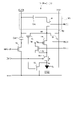
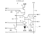
- FIG. 7 is a circuit diagram showing the configuration of the pixel circuit 15 in this embodiment.
- FIG. 4 is a circuit diagram showing a configuration of a j-th pixel circuit Pix(i,j) (1 ⁇ i ⁇ n, 1 ⁇ j ⁇ m);
- This pixel circuit like the pixel circuit 15a in the comparative example shown in FIG. 1 initialization transistor T1", “threshold compensation transistor T2", “data write control transistor T3", “driving transistor T4", "first emission control transistor T5", “second emission control transistor T6", “second initialization transistor T7”) and one data holding capacitor Cst.
- Transistors T1, T2 and T7 are N-type transistors.
- Transistors T3-T6 are P-type transistors.
- the N-type transistors T1, T2, and T7 are IGZO-TFTs
- the P-type transistors T3 to T6 are LTPS-TFTs, but they are not limited to this.
- the data holding capacitor Cst is a capacitive element having two electrodes consisting of a first electrode and a second electrode.
- the pixel circuit 15 in this embodiment includes a bias supply circuit 151 including a bias control transistor T8 and a bias holding capacitor Cbs. is provided.
- the transistors T1 to T3 and T5 to T8 other than the driving transistor T4 function as switching elements.
- the second scanning signal line two lines before the corresponding second scanning signal line NSi, that is, the i-2-th second scanning signal line (preceding second scanning signal line) NSi-2, the corresponding first scanning signal line line (corresponding first scanning signal line) PSi, corresponding emission control line (corresponding emission control line) EMi, corresponding data signal line (corresponding data signal line) Dj, initialization voltage line Vini, high level power supply line ELVDD , and a low-level power supply line ELVSS are connected.
- the bias control line BSi corresponding thereto is also connected.
- the pixel circuit Pix(i,j) may be connected to a second scanning signal line immediately preceding the corresponding second scanning signal line NSi instead of the preceding second scanning signal line NSi-2.
- the bias control transistor T8 and the bias holding capacitor Cbs are connected in series with each other.
- the bias control transistor T8 has a gate terminal connected to the corresponding bias control line BSi, and a node (hereinafter referred to as "first node ) has a drain terminal connected to N1.
- a source terminal of the drive transistor T4 is connected to the high level power supply line ELVDD via the bias control transistor T8 and the bias holding capacitor Cbs.
- the capacitance value of the bias holding capacitor Cbs is set to a value sufficiently larger than the capacitance value of the parasitic capacitance formed between the first node N1 and other nodes.
- FIG. 7 is a timing chart for explaining the operation of the pixel circuit Pix(i,j) during the non-light emitting period included in each frame period.
- the first scanning signal PS(i) and the second scanning signal NS for driving the pixel circuit 15 in this embodiment are the first scanning signal PS(i) for driving the pixel circuit 15a in the comparative example
- the 2 Scanning signals NS(i), NS(i-2), emission control signal EM(i), and data signal D(j) change in the same manner.
- the transistors T1 to T3 and T5 to T7 as switching elements included in the pixel circuit 15 in this embodiment are similar to the transistors T1 to T3 and T5 to T7 as switching elements included in the pixel circuit 15a in the comparative example. , and similar initialization and data write operations are performed.
- the first scanning signal PS(i) supplied to the pixel circuit 15a in the comparative example is the same as in the drive period TD (RF frame period Trf) as shown in FIG.
- the first scanning signal PS(i) applied to the pixel circuit 15 according to the present embodiment is maintained at H level as shown in FIG.
- the pixel circuit 15 of the present embodiment has a configuration in which the bias supply circuit 151 including the bias control transistor T8 and the bias holding capacitor Cbs is added to the pixel circuit of the comparative example (see FIG. 7). ), and a bias control signal BS(i) (hereinafter referred to as "corresponding bias control signal BS(i)”) is applied to the gate terminal of the bias control transistor T8 through a corresponding bias control line BSi.
- corresponding bias control signal BS(i) (hereinafter referred to as "corresponding bias control signal BS(i)”
- the bias control signal BS(i) changes from the L level to the H level at time t5, and changes from the H level to the L level at time t8. and change.
- the bias control signal BS(i) changes during the idle period TP (NRF frame period Tnrf) as well as during the drive period TD (RF frame period Trf). That is, the bias control signal BS(i) changes from the L level to the H level at time t12 and changes from the H level to the L level at time t13 during the non-light emitting period t11 to t14 within the NRF frame period Tnrf. do.
- FIG. 9 is a diagram showing the circuit state of the pixel circuit Pix(i, j) in this embodiment during each operation during the drive period TD.
- the pixel circuit 15 schematically shows the state of the pixel circuit Pix(i,j) during the initialization period t2 to t3, that is, the circuit state during the initialization operation.
- the state of the pixel circuit Pix(i, j) during the data write period t6 to t7 that is, the circuit state during the data write operation.
- j that is, the circuit state during the lighting operation.
- the bias control signal BS(i) is at H level during the period t5-t8 including the data write periods t6-t7, so the bias control transistor T8 is turned on during the data write periods t6-t7. is. Therefore, as can be seen from the pixel circuit 15 (WR) during the data write operation shown in FIG. 9, the voltage of the corresponding data signal line Dj (the voltage of the data signal D(j)) is is written in the data storage capacitor Cst as a data voltage via the data write control transistor T3 in the ON state and the drive transistor T4 in the diode connection state, and the data write control transistor T3 in the ON state and the bias control transistor in the ON state. It is also applied to bias holding capacitor Cbs through T8. Therefore, in the data write period t6 to t7, the voltage of the corresponding data signal line Dj at that time, that is, the data voltage Vdata is also written and held in the bias holding capacitor Cbs.
- FIG. 10 is a diagram showing the circuit state during each operation during the pause period TP for the pixel circuit Pix(i, j) in this embodiment.
- the pixel circuit 15 (OB) is the pixel circuit Pix(i,j ), that is, the circuit state during the on-bias application operation
- the pixel circuit 15 (NEM) is in the state of the pixel circuit Pix ( The state of i, j) is shown schematically.
- the data voltage is written to the data holding capacitor Cst while performing internal compensation as described above, thereby causing the voltage of the gate terminal of the driving transistor T4 (
- the gate voltage Vg) is the value given by the above equation (1).
- This gate voltage Vg corresponds to the holding voltage of the bias holding capacitor Cbs, and is maintained during the rest period TP immediately thereafter. Therefore, during the on-bias application period t12 to t13, a voltage corresponding to the threshold voltage Vth is applied between the gate and source of the driving transistor T4 regardless of the display grayscale indicated by the voltage held by the data holding capacitor Cst. Become. In the present embodiment, as shown in FIG.
- the emission control signal EM(i) and the bias control signal BS(i) change in the same way regardless of whether it is the drive period TD or the pause period TP.
- the on-bias voltage Vob as described above is applied between the gate and source of the driving transistor T4.
- the capacitance value of the bias holding capacitor Cbs is sufficiently larger than the capacitance value of the parasitic capacitance formed between the first node N1 and other nodes, the bias holding capacitor Cbs Even if the on-bias application is repeated a plurality of times during the pause period TP for one data voltage write, the voltage held by the bias holding capacitor Cbs does not substantially change.
- the pixel circuits Pix(1, 1) to Pix(n, m) of the display unit 11 receive the first scanning signals PS(1) to PS(1) to Pix(n, m) as shown in FIG. It is driven by PS(n), second scanning signals NS(-1) to NS(n), emission control signals EM(1) to EM(n), and data signals D(1) to D(m).
- the pixel circuits Pix(1,1) to Pix(n,m) of the display unit 11 receive the first scanning signal PS as shown in FIG. (1) to PS(n), second scanning signals NS(-1) to NS(n), bias control signals BS(1) to BS(n), emission control signals EM(1) to EM(n), It is driven by data signals D(1)-D(m).
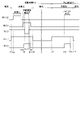
- FIG. 13 shows a luminance waveform (hereinafter referred to as “comparative luminance waveform”) La(i,j) of the pixel circuit Pix(i,j) in a comparative example based on the driving method shown in FIG. 11, and
- FIG. 3 shows a luminance waveform (hereinafter referred to as “luminance waveform of the present embodiment”) L(i, j) of the pixel circuit Pix(i, j) in the present embodiment based on the driving method.
- FIG. 14 shows the luminance waveform La(i, j) of the comparative example and the luminance waveform L(i, j) of the present embodiment so as to make it easier to see the difference between both luminance waveforms.
- a luminance waveform L(i, j) is indicated by a solid line
- a luminance waveform La(i, j) of the comparative example is indicated by a dotted line.
- the waveform (light-off waveform) indicating the light-off operation in the drive period TD (RF frame period Trf) and the idle period TP (NRF) There is a difference from the waveform (light-off waveform) indicating the light-off operation in the frame period Tnrf). More specifically, there is a difference in the rise of the luminance waveform when the pixel circuit Pix(i, j) changes from the off state to the on state due to the emission control signal EM(i) changing from the H level to the L level. .
- the emission control signal EM(i) changing from the H level to the L level.
- the rise of the luminance waveform in the NRF frame period Tnrf is steeper than the rise of the luminance waveform in the RF frame period Trf. It is considered that this is due to the hysteresis characteristic of the drive transistor T4.
- Such a difference in rise of the luminance waveform between the RF frame period Trf and the NRF frame period Tnrf is due to the corresponding data signal line Dj and the data signal line Dj from the data side drive circuit 30 during the on-bias application period t10 to t11 (see FIG. 4). It can be reduced by changing the on-bias voltage Vob applied to the source terminal of the drive transistor T4 via the write control transistor T3 (the pixel circuit 15a (OB )reference).
- the gate voltage Vg of the driving transistor T4 during the on-bias application period t10 to t11 depends on the display gradation indicated by the holding voltage of the data holding capacitor Cst. Therefore, in order to sufficiently reduce such a difference in rising waveform of the luminance waveform, the value of the on-bias voltage Vob to be applied to the pixel circuit Pix(i, j) is set to It is necessary to adjust according to the display gradation. However, such adjustment of the on-bias voltage Vob is difficult to achieve in the display device as the comparative example. Therefore, in the display device as the comparative example, the on-bias voltage Vob is usually set as a fixed value.
- the data voltage Vdata held in the bias holding capacitor Cbs is applied through the ON-state bias control transistor T8 during the ON bias application period t12 to t13. , is applied as an on-bias voltage Vob to the source terminal of the drive transistor T4 (see the pixel circuit 15 (OB) during the on-bias application operation shown in FIG. 10).
- the data voltage Vdata indicating the display gradation in each pixel circuit Pix(i, j) is applied to the source terminal of the drive transistor T4, thereby causing the drive transistor T4 to be energized during the on-bias application period t12 to t13.
- the gate-source voltage Vgs does not depend on the display gradation, and has a value substantially equal to the gate-source voltage Vgs of the driving transistor T4 during the data writing period t6 to t7 in the immediately preceding driving period TD.
- the difference in rising waveform of the luminance waveform between the RF frame period Trf and the NRF frame period Tnrf is sufficiently reduced in all pixel circuits 15 at the same time.
- flicker is simultaneously suppressed in the entire area of the displayed image, and even if the optimum value of the on-bias voltage Vob deviates due to other factors affecting flicker, the flicker becomes less visible.
- FIG. 1 This organic EL display device has first bias control lines BS11 to BS1n as bias write control lines and bias control lines as bias application control lines instead of the bias control lines BS1 to BSn in the display device according to the first embodiment.
- Second bias control lines BS21 to BS2n are provided, and each pixel circuit in the present embodiment corresponds to any one of the n first bias control lines BS11 to BS1n, and n second bias control lines BS11 to BS1n. It corresponds to any one of the control lines BS21 to BS2n.
- the scanning-side drive circuit applies first bias control signals BS1(1) to BS1(n) to first bias control lines BS11 to BS1n, respectively, and applies second bias control signals BS2(n) to second bias control lines BS21 to BS2n. 1) to BS2(n) are applied.
- the pixel circuit in this embodiment is provided with a bias supply circuit as in the pixel circuit in the first embodiment. is different from the configuration of the bias supply circuit in .
- Other configurations of the display device according to the present embodiment are basically the same as those of the display device according to the first embodiment. Description is omitted (see FIGS. 1 and 2).
- FIG. 15 is a circuit diagram showing the configuration of the pixel circuit 16 in this embodiment.
- FIG. 4 is a circuit diagram showing a configuration of a j-th pixel circuit Pix(i,j) (1 ⁇ i ⁇ n, 1 ⁇ j ⁇ m);
- This pixel circuit 16 has the same configuration as the pixel circuit 15 (FIG. 7) in the first embodiment except for the configuration of the bias supply circuit 152 .
- the components other than the bias supply circuit 152 are denoted by the same reference numerals as the components included in the pixel circuit 15 in the first embodiment. A detailed explanation is omitted.
- the pixel circuit Pix(i, j) of the i-th row and the j-th column which is the pixel circuit 16 in this embodiment, includes the corresponding first scanning signal line PSi, the corresponding second scanning signal line NSi, the preceding
- the corresponding emission control line EMi the corresponding data signal line Dj
- the initialization voltage line Vini the high level power supply line ELVDD
- the low level power supply line ELVSS the pixel circuit Pix(i , j) are connected to the first and second bias control lines BS1i and BS2i.
- a bias supply circuit 152 provided in the pixel circuit 16 includes a bias application control transistor T8, a bias write control transistor T9, a bias holding capacitor Cbs1, and a voltage dividing capacitor Cbs2.
- the bias write control transistor T9 has a gate terminal connected to a first bias control line (hereinafter referred to as "corresponding first bias control line”) BS1i corresponding to the pixel circuit Pix(i, j), and a switching element. function as
- the bias application control transistor T8 has a gate terminal connected to a second bias control line (hereinafter referred to as a "corresponding second bias control line”) BS2i corresponding to the pixel circuit Pix(i,j). It functions as a switching element corresponding to the bias control transistor T8 in the first embodiment.
- the source terminal of the driving transistor T4 is connected to the high-level power supply line ELVDD through the bias application control transistor T8 and the bias holding capacitor Cbs1 in this order, and is connected to the bias holding voltage through the bias write control transistor T9 and the voltage dividing capacitor Cbs2. It is connected to the connection point between the capacitor Cbs1 and the bias application control transistor T8. Also in this embodiment, the source terminal of the drive transistor T4 is connected to the corresponding data signal line Dj through the data write control transistor T3, so the corresponding data signal line Dj is connected to the bias write control transistor T9 and the voltage dividing transistor T9. Through the capacitor Cbs2, it is connected to the connection point between the bias application control transistor T8 and the bias holding capacitor Cbs1. The bias holding capacitor Cbs1 and the voltage dividing capacitor Cbs2 are connected in series to form a voltage dividing circuit.
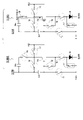
- FIG. 16 is a timing chart for explaining the operation of the pixel circuit Pix(i,j) during the non-light emitting period included in each frame period.
- the first scanning signal PS(i) for driving the pixel circuit Pix(i, j) in this embodiment corresponds to the pixel circuit Pix(i, j) in the first embodiment.
- the first scanning signal PS(i) for driving, the second scanning signals NS(i) and NS(i-2), the light emission control signal EM(i), and the data signal D(j) change in the same manner. .
- the transistors T1 to T3 and T5 to T7 serving as switching elements included in the pixel circuit 15 of the present embodiment are replaced with the transistors T1 to T3 and T5 serving as switching elements included in the pixel circuit 15 of the first embodiment.
- the same initialization operation and data write operation are performed.
- the gate terminal of the bias write control transistor T9 is connected to the first bias control line BS1i through the corresponding first bias control line BS1i.
- a signal BS1(i) (hereinafter referred to as a “corresponding first bias control signal BS1(i)”) is applied as a bias write control signal, and a corresponding second bias control line BS2i is connected to the gate terminal of the bias application control transistor T8.
- a second bias control signal BS2(i) (hereinafter referred to as a “corresponding second bias control signal BS2(i)”) is applied as a bias application control signal via the second bias control signal BS2(i). As shown in FIG.
- the corresponding first bias control signal BS1(i) changes from L level to H level at time t5, and changes from H level to L level at time t8. change to level.
- the first bias control signal BS1(i) is maintained at low level during the pause period TP (NRF frame period Tnrf).
- the corresponding second bias control signal BS2(i) is maintained at a low level during the driving period TD (RF frame period Trf), and during the non-light emitting period t11 to t14 during the pause period TP (NRF frame period Tnrf). , and changes from H level to L level at time t13.
- FIG. 17 is a diagram showing the circuit state during each operation during the drive period TD for the pixel circuit Pix(i, j) in this embodiment.
- the pixel circuit 16 (INI) schematically shows the state of the pixel circuit Pix(i, j) during the initialization period t2 to t3, that is, the circuit state during the initialization operation, and the pixel circuit 16 (WR) , the state of the pixel circuit Pix(i, j) during the data write period t6 to t7, that is, the circuit state during the data write operation. , j), that is, the circuit state during the lighting operation.
- FIG. 18 is a diagram showing circuit states during each operation during the pause period TP for the pixel circuit Pix(i, j) in this embodiment.
- the pixel circuit 16 (NEM) is the pixel circuit Pix ( i, j)
- the pixel circuit 16 (OB) is in the on-bias application period t12-t13 in which the corresponding second bias control signal BS2(i) is at H level during the non-light-emitting period t11-t14.
- 2 schematically shows the state of the pixel circuit Pix(i, j) of , that is, the circuit state during the on-bias application operation.
- the data write control transistor T3, the first emission control transistor T5, and the bias The write control transistor T9 is in an off state and the bias application control transistor T8 is in an on state (see the pixel circuit 16 (OB) during the on-bias application operation shown in FIG. 18).
- the voltage difference between the data voltage Vdata held in the voltage dividing circuit and the high-level power supply voltage ELVDD during the data writing period t6 to t7 in the immediately preceding driving period TD is transferred to the bias holding capacitor Cbs1 and the voltage dividing capacitor Cbs2.
- a voltage obtained by dividing the voltage by V that is, a voltage Vob expressed by the following equation is applied to the source terminal of the driving transistor T4 as an on-bias voltage.
- symbols "Cbs1" and “Cbs2” denote the capacitance values of the bias holding capacitor Cbs1 and the voltage dividing capacitor Cbs2, respectively.
- Vob ELVDD+(Vdata ⁇ ELVDD) ⁇ Cbs2/(Cbs1+Cbs2) ⁇ ...(2)
- the on-bias voltage Vob applied to the source terminal of the driving transistor T4 in each pixel circuit 16 can be adjusted by the capacitance ratio Cbs1/Cbs2 as shown in the above equation (2). Therefore, according to the present embodiment, by setting the capacitance ratio Cbs1/Cbs2, the same effects as those of the first embodiment can be obtained more reliably.
- FIG. 19 is a circuit diagram showing a configuration example when the present invention is applied to a pixel circuit (see JP-A-2019-211775) using an N-type LTPS-TFT as the drive transistor T4.
- the pixel circuit 17 shown in FIG. 19 includes one organic EL element OL as a display element, an initialization transistor T1, a threshold compensation transistor T2, a data write control transistor T3, a drive transistor T4, and a first light emission. It includes a control transistor T5, a second emission control transistor T6, and one data holding capacitor Cst, and these components T1 to T6, Cst, and OL are connected as shown in FIG.
- the pixel circuit 17 is also provided with a bias supply circuit 151 including a bias control transistor T8 and a bias holding capacitor Cbs connected in series.
- the source terminal of the drive transistor T4 is connected to the low level power supply line ELVSS via the bias control transistor T8 and the bias holding capacitor Cbs.
- the first scanning signal lines PS1 to PSn and the second scanning signal lines NS-1 to NSn (FIG. 1 ), the first scanning signal lines NS11 to NS1n for transmitting the first scanning signals NS1(1) to NS1(n), respectively, and the second scanning signals NS2(1) to NS2(n), respectively.
- Second scanning signal lines NS21 to NS2n for transmission and third scanning signal lines NS31 to NS3n for transmitting the third scanning signals NS3(1) to NS3(n), respectively, are arranged in the display section 11. It is Further, in the display device according to this modification, first emission control signals EM1(1) to EM1(n) are respectively transmitted instead of the emission control lines EM1 to EMn (see FIG. 1) in the first embodiment.
- the display unit 11 is provided with first emission control lines EM11 to EM1n for transmitting second emission control signals EM2(1) to EM2(n), and second emission control lines EM21 to EM2n for transmitting the second emission control signals EM2(1) to EM2(n), respectively.
- Other configurations in this modification are basically the same as those in the first embodiment.
- a first emission control signal EM1(i), a second emission control signal EM2(i), and a bias control signal BS(i) are provided.
- the initialization operation is performed during the periods t2 to t3 of the non-light emitting periods t1 to t8 in the drive period TD (refresh frame period), and the data is held during the periods t5 to t6.
- Data voltage Vdata is written with internal compensation to capacitor Cst. Since the bias control transistor T8 is on during the period t4-t7, the data voltage Vdata is also written to the bias holding capacitor Cbs through the bias control transistor T8 during the period t5-t6.
- the data write control transistor T3 is P-type, and the threshold compensation transistor T2 and the first initialization transistor T1 are N-type. It may be a conductive type. For example, these transistors T1 to T3 may all be P-type.
- n+2 scanning signal lines serving as the first scanning signal lines PS1 to PSn and the second scanning signal lines NS-1 to NSn may be arranged in the display section 11. FIG. In this way, the number of scanning signal lines can be reduced to about half compared with the above-described embodiments, and the configurations of the display section 11 and the scanning-side driving circuit 40 are simplified.
- the bias control transistor T8 controls the writing of the data voltage to the bias holding capacitor Cbs and also controls the voltage held in the bias holding capacitor Cbs (on-bias voltage Vob). is applied to the drive transistor T4.
- the function of the bias control transistor T8 may be realized by two transistors. That is, instead of the bias control transistor T8, a bias write control transistor for controlling writing of the data voltage to the bias holding capacitor Cbs and application of the holding voltage (on-bias voltage Vob) in the bias holding capacitor Cbs to the drive transistor T4. may be configured to use a bias application control transistor for controlling .
- the pixel circuit has, for example, the connection point between the bias control transistor T8 and the bias holding capacitor Cbs in the configuration shown in FIG. is configured to function as a bias application control transistor.
- first and second bias control signals BS1(i) and BS2(i) as shown in FIG. 16 are applied to the gate terminal of the bias write control transistor and the gate terminal of the bias application control transistor, respectively. be done.
- the pixel circuit 15 configured as shown in FIG. 7 or the pixel circuit 16 configured as shown in FIG. 15 is used. is not limited to the configurations shown in FIGS. 7 and 15, either.
- the pixel circuits (FIGS. 7 and 15) in the above-described embodiments are configured to perform threshold compensation by diode connection of the drive transistor T4. It is also applicable to a pixel circuit without a threshold compensation function).
- FIG. 21 shows a configuration example in which the present invention is applied to a pixel circuit that does not perform threshold compensation by diode connection of the driving transistor T4, that is, a configuration example in which a bias supply circuit is provided in a pixel circuit without a threshold compensation function.
- the pixel circuit 18 shown in FIG. 21 includes one organic EL element OL as a display element, a data write control transistor T3, a drive transistor T4, a first emission control transistor T5, and a second emission control transistor T6. , an initialization transistor T7 and one data holding capacitor Cst, and these components T3-T7, Cst, OL are connected as shown in FIG.
- the pixel circuit 18 is also provided with a bias supply circuit 152 including a bias application control transistor T8 and a bias holding capacitor Cbs connected in series, and a bias write control transistor T9.
- the source terminal of the drive transistor T4 is connected to the high level power supply line ELVDD through the bias application control transistor T8 and the bias holding capacitor Cbs.
- the data signal line Dj corresponding to the pixel circuit 18 is connected via the bias write control transistor T9 to the connection point between the bias application control transistor T8 and the bias holding capacitor Cbs.
- the first bias control signal BS1 (see FIG. 1) is used.
- FIG. 22 shows the pixel circuit 18 of FIG. 21 configured as described above, that is, the pixel circuit 18 corresponding to the i-th scanning signal line PSi and the j-th data signal line Dj, i-th row and j-th column pixel circuit.
- 4 is a timing chart for explaining the operation of Pix(i, j), more specifically timing for explaining the operation of the pixel circuit Pix(i, j) during a non-light emitting period included in each frame period; Chart.
- a first scanning signal PS(i), an emission control signal EM(i), a first bias control signal BS1(i), and a first bias control signal BS1(i) which change as shown in FIG.
- a second bias control signal BS2(i) is provided.
- the voltage of the data signal line Dj corresponding to the data holding capacitor Cst in the period t4 to t5 among the non-light emitting periods t1 to t8 in the drive period TD (refresh frame period) is the data.
- the voltage of the corresponding data signal line Dj is written to the bias holding capacitor Cbs via the bias write control transistor T9.
- the voltage of the corresponding data signal line Dj written to the bias holding capacitor Cbs is a voltage corresponding to the data voltage Vdata written to the data holding capacitor Cst, but not the same level as the data voltage Vdata.
- This voltage is set so as to eliminate or reduce the difference between the voltage stress applied during the non-light-emitting period within the drive period TD and the voltage stress applied during the non-light-emitting period within the pause period TP for T4.
- such a voltage is applied from the corresponding data signal line Dj to the bias holding capacitor Cbs in the pixel circuit Pix(i,j) during the period t6 to t7.
- the data side drive circuit 30 drives the data signal lines D1 to Dm.
- the voltage (voltage corresponding to the data voltage Vdata) held in the bias holding capacitor Cbs is biased.
- An on-bias voltage Vob is applied to the source terminal of the drive transistor T4 via the application control transistor T8.
- the period t5 to t8 during which the corresponding bias control signal BS(i) or the corresponding first bias control signal BS1(i) is at the H level in the drive period TD is the corresponding second Although shorter than the period t4-t9 in which the scanning signal NS(i) is at H level and longer than the data write period t6-t7 (see FIGS.
- the corresponding bias control signal BS(i) or the corresponding th The period t5 to t8 in which the 1 bias control signal BS1(i) is at H level is set to the same length as the period t4 to t9 in which the corresponding second scanning signal NS(i) is at H level or the data write period t6 to t7. good too.
- the on-bias application period t12 to t13 in the pause period TP is longer than the data write period t6 to t7 (FIGS. 8 and 16), but the on-bias application period t12 ⁇ t13 may have the same length as the data write period t6 to t7 or a length shorter than the data write period t6 to t7.
- each embodiment has been described by taking the organic EL display device as an example, but the present invention is not limited to the organic EL display device, and the pause driving is performed using the display element driven by current.
- Any display device that performs Display elements that can be used here include, for example, organic EL elements, namely organic light emitting diodes (OLED), inorganic light emitting diodes and quantum dot light emitting diodes (Quantum dot Light Emitting Diode (QLED)). be.
- Cst Data holding capacitor
- Cbs Bias holding capacitor
- Cbs2 Voltage dividing capacitor
- T1 First initialization transistor (first initialization switching element) T2 ...
- threshold compensation transistor threshold compensation switching element T3 ... data write control transistor (data write control switching element) T4: drive transistor T5: first emission control transistor (first emission control switching element) T6 ... second emission control transistor (second emission control switching element) T7 ... second initialization transistor (second initialization switching element) T8 ... bias control transistor (bias control switching element), Bias application control transistor (bias application control switching element) T9 ... bias write control transistor (bias write control switching element) TD ... drive period TP ... pause period Trf ... refresh frame period (RF frame period) Tnrf: non-refresh frame period (NRF frame period) Vob ... On-bias voltage
Abstract
The present invention discloses a current-drive-type display device such as an organic EL display device, said display device being capable of providing a good display without perceptible flicker in all regions of a display screen even if driving is paused. Each pixel circuit 15 is provided with a bias supply circuit 151 that includes a bias holding capacitor Cbs and a bias control transistor T8 that are connected in series. In a paused drive mode, light emission control lines and bias control lines are driven during both drive periods and pause periods. By controlling the bias control transistor using the bias control line, during drive periods, the voltage of a data signal line Dj is also written to the bias holding capacitor Cbs when being written to a data holding capacitor Cst, and during pause periods, the voltage written to the bias holding capacitor Cbs is applied to the source terminal of the drive transistor during on-bias application periods within non-light-emission periods.
Description
本開示は、有機EL(Electro Luminescence)素子等の電流で駆動される表示素子を備えた電流駆動型の表示装置に関するものであり、特に、当該表示装置で使用される画素回路に関する。
The present disclosure relates to a current-driven display device having a display element driven by current, such as an organic EL (Electro Luminescence) element, and particularly to a pixel circuit used in the display device.
近年、有機EL素子(有機発光ダイオード(Organic Light Emitting Diode: OLED)とも呼ばれる)を含む画素回路を備えた有機EL表示装置が実用化されている。有機EL表示装置の画素回路は、有機EL素子に加えて、駆動トランジスタや、書込制御トランジスタ、保持キャパシタ等を含んでいる。駆動トランジスタや書込制御トランジスタには、薄膜トランジスタ(Thin Film Transistor)が使用され、駆動トランジスタの制御端子としてのゲート端子に保持キャパシタが接続され、この保持キャパシタには、駆動回路からデータ信号線を介して、表示すべき画像を表す映像信号に応じた電圧(より詳しくは、当該画素回路で形成すべき画素の階調値を示す電圧)がデータ電圧として与えられる。有機EL素子は、それに流れる電流に応じた輝度で発光する自発光型表示素子である。駆動トランジスタは、有機EL素子と直列に設けられ、保持キャパシタに保持される電圧にしたがって、有機EL素子に流れる電流を制御する。
In recent years, organic EL display devices equipped with pixel circuits including organic EL elements (also called organic light emitting diodes (OLEDs)) have been put to practical use. A pixel circuit of an organic EL display device includes a drive transistor, a write control transistor, a holding capacitor, etc. in addition to the organic EL element. A thin film transistor is used for the drive transistor and the write control transistor, and a holding capacitor is connected to the gate terminal as the control terminal of the drive transistor. A voltage corresponding to a video signal representing an image to be displayed (more specifically, a voltage representing a gradation value of a pixel to be formed by the pixel circuit) is applied as a data voltage. An organic EL element is a self-luminous display element that emits light with a luminance corresponding to the current flowing through it. The drive transistor is provided in series with the organic EL element and controls the current flowing through the organic EL element according to the voltage held in the holding capacitor.
一方、低消費電力の表示装置として、休止駆動を行う表示装置が知られている。休止駆動とは、同じ画像を続けて表示するときに駆動期間(リフレッシュ期間)と休止期間(非リフレッシュ期間)を設け、駆動期間では駆動回路を動作させ、休止期間では駆動回路の動作を停止させる駆動方法であり、「間欠駆動」または「低周波駆動」とも呼ばれる。休止駆動は、画素回路に含まれるスイッチング素子としてのトランジスタのオフリーク電流が小さい場合に適用できる。オフリーク電流が小さいトランジスタとして、チャネル層が酸化物半導体で形成された薄膜トランジスタ(以下「酸化物TFT」という)が知られており、典型的には、酸化物半導体として酸化インジウムガリウム亜鉛(InGaZnO)を採用した酸化物TFT(以下「IGZO-TFT」という。)が使用されている。このことから、画素回路において、移動度の高い低温ポリシリコンでチャネル層が形成された薄膜トランジスタ(以下「LTPS-TFT」という)を駆動トランジスタとして使用しつつ、オフリーク電流が小さいIGZO-TFTをスイッチング素子として使用し、そのような画素回路により構成される表示部に対して休止駆動を行う有機EL表示装置が提案されている(例えば米国特許出願公開第2020/0118487号明細書参照)。
On the other hand, a display device that performs pause driving is known as a display device with low power consumption. In pause driving, when the same image is displayed continuously, a drive period (refresh period) and a rest period (non-refresh period) are provided, the drive circuit is operated during the drive period, and the operation of the drive circuit is stopped during the rest period. It is a driving method, and is also called "intermittent driving" or "low frequency driving". Pause driving can be applied when the off-leakage current of a transistor as a switching element included in a pixel circuit is small. As a transistor with a small off-leakage current, a thin film transistor (hereinafter referred to as an "oxide TFT") having a channel layer formed of an oxide semiconductor is known. Typically, indium gallium zinc oxide (InGaZnO) is used as the oxide semiconductor. The adopted oxide TFT (hereinafter referred to as “IGZO-TFT”) is used. For this reason, in the pixel circuit, a thin film transistor (hereinafter referred to as "LTPS-TFT") having a channel layer formed of low-temperature polysilicon with high mobility is used as a driving transistor, and an IGZO-TFT having a small off-leak current is used as a switching element. An organic EL display device has been proposed in which a display unit configured by such a pixel circuit is used as a pixel circuit and performs pause driving (see, for example, US Patent Application Publication No. 2020/0118487).
有機EL表示装置において休止駆動を行う場合、駆動期間では、各画素回路の有機EL素子は、フレーム期間毎に設けられる非発光期間に発光制御トランジスタにより消灯状態とされるが、休止期間では、駆動回路の動作が停止し、各画素回路の有機EL素子は、その前の駆動期間において書き込まれたデータ電圧に応じた輝度で発光を続ける。一般に、休止期間は駆動期間に比べ格段に長く(例えば、駆動期間は1または数フレーム期間から構成され、休止期間は数十フレーム期間から構成される)、休止駆動方式の有機EL表示装置では動作中に、そのような駆動期間と休止期間とが交互に現れる。このため、このような休止駆動を行うと、駆動期間における有機EL素子の消灯がフリッカとして視認されることになる。
When rest driving is performed in an organic EL display device, the organic EL element of each pixel circuit is turned off by the light emission control transistor during a non-light emitting period provided for each frame period in the driving period. The operation of the circuit stops, and the organic EL element of each pixel circuit continues to emit light with a luminance corresponding to the data voltage written in the previous driving period. In general, the pause period is much longer than the drive period (for example, the drive period consists of one or several frame periods, and the pause period consists of several tens of frame periods). , such drive periods and rest periods alternate. Therefore, when such a pause drive is performed, the off-lighting of the organic EL element during the drive period is visually recognized as flicker.
これに対し米国特許出願公開第2019/0057646号明細書には、休止駆動(低周波駆動)を行う場合に視認されるフリッカを解消すべく、駆動期間(データリフレッシュ期間T_refrech)での有機EL素子(発光ダイオード304)の消灯による輝度低下に加えて、休止期間(拡張ブランキング期間T_blank)においても適切な頻度での消灯により輝度低下が生じるように構成された画素回路とその駆動方法が記載されている(段落[0049]~[0052]、図8A,8B,9A,9B参照)。
On the other hand, in US Patent Application Publication No. 2019/0057646, in order to eliminate visible flicker when performing pause driving (low-frequency driving), the organic EL element during the driving period (data refresh period T_refrech) A pixel circuit and a driving method thereof are described, which are configured so that, in addition to luminance reduction due to turning off the (light emitting diode 304), luminance reduction occurs due to turning off at an appropriate frequency even in a pause period (extended blanking period T_blank). (paragraphs [0049] to [0052], see FIGS. 8A, 8B, 9A, and 9B).
しかし、休止期間においても適切な頻度での消灯により輝度低下が生じるように構成されていても(以下このような構成を「周期的消灯構成」という)、画素回路における駆動トランジスタとしての薄膜トランジスタはヒステリシス特性を有することから、低周波駆動(休止駆動)において依然としてフリッカが視認される。すなわち、この周期的消灯構成では、駆動トランジスタとしての薄膜トランジスタに加わる電圧ストレスが駆動期間と休止期間とで異なることから、その駆動トランジスタのヒステリシス特性のために駆動期間と休止期間とで消灯波形が若干異なり、これによりフリッカが視認される。
However, even if it is configured so that the luminance is lowered by turning off lights at an appropriate frequency even in the idle period (such a configuration is hereinafter referred to as a "periodic turning off configuration"), the thin film transistor as the driving transistor in the pixel circuit has hysteresis. Due to its characteristic, flicker is still visible in low frequency drive (pause drive). That is, in this periodic light-off configuration, the voltage stress applied to the thin film transistor as the drive transistor differs between the drive period and the rest period. Unlike, this makes the flicker visible.
このような駆動トランジスタのヒステリシス特性に起因するフリッカの発生を抑制するために、休止期間において駆動トランジスタに意図的にバイアスストレス電圧(以下「オンバイアス電圧」または単に「バイアス電圧」という)を印加することが提案されている(例えば米国特許出願公開第2020/0118487号明細書、日本国特開2020-112795号公報参照)。しかし、このように休止期間において意図的にバイアス電圧を印加しても、必ずしも表示画像の全領域においてフリッカを抑制できず、フリッカが依然として視認されうることが本願発明者により確認されている。
In order to suppress the occurrence of flicker due to such hysteresis characteristics of the drive transistor, a bias stress voltage (hereinafter referred to as "on-bias voltage" or simply "bias voltage") is applied intentionally to the drive transistor during the idle period. (See, for example, US Patent Application Publication No. 2020/0118487 and Japanese Patent Application Publication No. 2020-112795). However, the inventors of the present application have confirmed that even if the bias voltage is applied intentionally in the rest period, the flicker cannot necessarily be suppressed in the entire area of the display image, and the flicker can still be visually recognized.
そこで、有機EL表示装置のような電流駆動型の表示装置において休止駆動を行っても表示画像の全領域においてフリッカの視認されない良好な表示を行えるようにすることが望まれる。
Therefore, it is desired that a current-driven display device such as an organic EL display device be able to perform good display without visible flicker in the entire area of the display image even if the pause drive is performed.
本発明の幾つかの実施形態に係る画素回路は、複数のデータ信号線と複数の第1走査信号線と複数の発光制御線と第1および第2電源線とを含む表示部を有する表示装置において、前記複数のデータ信号線のいずれか1つに対応し、かつ、前記複数の第1走査信号線のいずれか1つに対応し、かつ、前記複数の発光制御線のいずれか1つに対応するように設けられた画素回路であって、
電流によって駆動される表示素子と、
制御端子と第1導通端子と第2導通端子とを有し前記表示素子と直列に設けられた駆動トランジスタと、
データ保持キャパシタと、
対応する第1走査信号線に接続された制御端子を有し、対応するデータ信号線の電圧の前記データ保持キャパシタへの書き込みを制御するデータ書込制御スイッチング素子と、
対応する発光制御線に接続された制御端子を有する第1発光制御スイッチング素子と、
バイアス供給回路とを備え、
前記表示部は、複数のバイアス制御線を更に含み、
当該画素回路は、複数のバイアス制御線のいずれか1つに対応し、
前記バイアス供給回路は、
前記対応するデータ信号線の電圧に応じた電圧を保持するためのバイアス保持キャパシタと、
対応するバイアス制御線に接続された制御端子を有し前記バイアス保持キャパシタに直列に接続されたバイアス制御スイッチング素子とを含み、
前記駆動トランジスタの前記制御端子は、前記データ保持キャパシタを介して固定電圧線に接続されており、
前記駆動トランジスタの前記第1導通端子は、前記第1発光制御スイッチング素子を介して前記第1電源線に接続されるとともに、前記バイアス制御スイッチング素子および前記バイアス保持キャパシタを介して固定電圧線に接続されている。 A pixel circuit according to some embodiments of the present invention is a display device having a display section including a plurality of data signal lines, a plurality of first scanning signal lines, a plurality of emission control lines, and first and second power supply lines. in any one of the plurality of data signal lines, corresponding to any one of the plurality of first scanning signal lines, and any one of the plurality of emission control lines A correspondingly arranged pixel circuit comprising:
a display element driven by a current;
a drive transistor having a control terminal, a first conduction terminal, and a second conduction terminal and provided in series with the display element;
a data retention capacitor;
a data write control switching element having a control terminal connected to a corresponding first scanning signal line and controlling writing of the voltage of the corresponding data signal line to the data holding capacitor;
a first emission control switching element having a control terminal connected to a corresponding emission control line;
a bias supply circuit;
The display unit further includes a plurality of bias control lines,
the pixel circuit corresponds to one of the plurality of bias control lines,
The bias supply circuit is
a bias holding capacitor for holding a voltage corresponding to the voltage of the corresponding data signal line;
a bias control switching element connected in series with the bias holding capacitor having a control terminal connected to a corresponding bias control line;
the control terminal of the drive transistor is connected to a fixed voltage line through the data holding capacitor;
The first conduction terminal of the drive transistor is connected to the first power supply line via the first light emission control switching element and to a fixed voltage line via the bias control switching element and the bias holding capacitor. It is
本発明の幾つかの実施形態に係る表示装置は、
複数のデータ信号線、複数の第1走査信号線、複数の発光制御線、複数のバイアス制御線、第1電源線、第2電源線、および、複数の画素回路を含む表示部と、
複数のデータ信号を生成して前記複数のデータ信号線に印加するデータ側駆動回路と、
前記複数の第1走査信号線を選択的に駆動し、前記複数の発光制御線を選択的に駆動し、前記複数のバイアス制御線を選択的に駆動する走査側駆動回路と、
前記複数の画素回路に前記複数のデータ信号の電圧をデータ電圧として書き込むリフレッシュフレーム期間からなる駆動期間と前記複数の画素回路へのデータ電圧の書き込みを停止する非リフレッシュフレーム期間からなる休止期間とが交互に現れるように、前記データ側駆動回路および前記走査側駆動回路を制御する表示制御回路とを備え、
前記複数の画素回路のそれぞれは、
前記複数のデータ信号線のいずれか1つに対応し、かつ、前記複数の第1走査信号線のいずれか1つに対応し、かつ、前記複数の発光制御線のいずれか1つに対応し、かつ、複数のバイアス制御線のいずれか1つに対応し、
電流によって駆動される表示素子と、制御端子と第1導通端子と第2導通端子とを有し前記表示素子と直列に設けられた駆動トランジスタと、データ保持キャパシタと、対応する第1走査信号線に接続された制御端子を有し対応するデータ信号線の電圧の前記データ保持キャパシタへの書き込みを制御するデータ書込制御スイッチング素子と、対応する発光制御線に接続された制御端子を有する第1発光制御スイッチング素子と、バイアス供給回路とを含み、
前記複数の画素回路のそれぞれにおいて、
前記バイアス供給回路は、前記対応するデータ信号線の電圧に応じた電圧を保持するためのバイアス保持キャパシタと、対応するバイアス制御線に接続された制御端子を有し前記バイアス保持キャパシタに直列に接続されたバイアス制御スイッチング素子とを含み、
前記駆動トランジスタの前記制御端子は、前記データ保持キャパシタを介して固定電圧線に接続されており、
前記駆動トランジスタの前記第1導通端子は、前記第1発光制御スイッチング素子を介して前記第1電源線に接続されるとともに、前記バイアス制御スイッチング素子および前記バイアス保持キャパシタを介して固定電圧線に接続されており、
前記表示制御回路は、
前記駆動期間では、前記第1発光制御スイッチング素子がオフ状態のときに前記対応するデータ信号線の電圧がデータ電圧として前記データ保持キャパシタに書き込まれて保持されるとともに当該データ電圧に応じた電圧が前記バイアス保持キャパシタに書き込まれて保持され、前記第1発光制御スイッチング素子がオン状態のときに前記データ保持キャパシタの保持電圧に応じた電流が前記表示素子に流れるように、前記データ側駆動回路および前記走査側駆動回路を制御し、
前記休止期間では、前記第1発光制御スイッチング素子がオフ状態のときに前記バイアス保持キャパシタの保持電圧が前記バイアス制御スイッチング素子を介して前記駆動トランジスタの前記第1導通端子に印加され、前記第1発光制御スイッチング素子がオン状態のときに前記データ保持キャパシタの保持電圧に応じた電流が前記表示素子に流れるように、前記走査側駆動回路を制御する。 A display device according to some embodiments of the present invention comprises:
a display unit including a plurality of data signal lines, a plurality of first scanning signal lines, a plurality of emission control lines, a plurality of bias control lines, a first power supply line, a second power supply line, and a plurality of pixel circuits;
a data side driver circuit that generates a plurality of data signals and applies them to the plurality of data signal lines;
a scanning side drive circuit that selectively drives the plurality of first scanning signal lines, selectively drives the plurality of emission control lines, and selectively drives the plurality of bias control lines;
A driving period consisting of a refresh frame period for writing the voltages of the plurality of data signals to the plurality of pixel circuits as data voltages, and a rest period consisting of a non-refresh frame period for stopping writing of the data voltages to the plurality of pixel circuits. a display control circuit for controlling the data-side driving circuit and the scanning-side driving circuit so as to appear alternately;
each of the plurality of pixel circuits,
corresponds to any one of the plurality of data signal lines, corresponds to any one of the plurality of first scanning signal lines, and corresponds to any one of the plurality of emission control lines; , and corresponding to any one of the plurality of bias control lines,
a display element driven by current; a drive transistor having a control terminal, a first conduction terminal and a second conduction terminal and provided in series with the display element; a data holding capacitor; and a corresponding first scanning signal line. a data write control switching element for controlling writing of the voltage of the corresponding data signal line to the data holding capacitor and having a control terminal connected to the corresponding light emission control line; including a light emission control switching element and a bias supply circuit,
In each of the plurality of pixel circuits,
The bias supply circuit has a bias holding capacitor for holding a voltage corresponding to the voltage of the corresponding data signal line, and a control terminal connected to the corresponding bias control line, and is connected in series with the bias holding capacitor. and a bias-controlled switching element;
the control terminal of the drive transistor is connected to a fixed voltage line through the data holding capacitor;
The first conduction terminal of the drive transistor is connected to the first power supply line via the first light emission control switching element and to a fixed voltage line via the bias control switching element and the bias holding capacitor. has been
The display control circuit is
In the drive period, the voltage of the corresponding data signal line is written and held as the data voltage in the data holding capacitor when the first light emission control switching element is in an off state, and a voltage corresponding to the data voltage is produced. The data-side driving circuit and the controlling the scanning side drive circuit;
In the idle period, when the first light emission control switching element is in an off state, the voltage held by the bias holding capacitor is applied to the first conduction terminal of the driving transistor through the bias control switching element. The scanning side drive circuit is controlled such that a current corresponding to the voltage held by the data holding capacitor flows through the display element when the light emission control switching element is in an ON state.
本発明の幾つかの実施形態に係る駆動方法は、複数のデータ信号線と複数の第1走査信号線と複数の発光制御線と第1および第2電源線と複数の画素回路とを含む表示部を有する表示装置の駆動方法であって、
前記表示部は、複数のバイアス制御線を更に含み、
前記複数の画素回路のそれぞれは、
前記複数のデータ信号線のいずれか1つに対応し、かつ、前記複数の第1走査信号線のいずれか1つに対応し、かつ、前記複数の発光制御線のいずれか1つに対応し、かつ、複数のバイアス制御線のいずれか1つに対応し、
電流によって駆動される表示素子と、制御端子と第1導通端子と第2導通端子とを有し前記表示素子と直列に設けられた駆動トランジスタと、データ保持キャパシタと、対応する第1走査信号線に接続された制御端子を有し対応するデータ信号線の電圧の前記データ保持キャパシタへの書き込みを制御するデータ書込制御スイッチング素子と、対応する発光制御線に接続された制御端子を有する第1発光制御スイッチング素子と、バイアス供給回路とを含み、
前記複数の画素回路のそれぞれにおいて、
前記バイアス供給回路は、前記対応するデータ信号線の電圧に応じた電圧を保持するためのバイアス保持キャパシタと、対応するバイアス制御線に接続された制御端子を有し前記バイアス保持キャパシタに直列に接続されたバイアス制御スイッチング素子とを含み、
前記駆動トランジスタの前記制御端子は、前記データ保持キャパシタを介して固定電圧線に接続されており、
前記駆動トランジスタの前記第1導通端子は、前記第1発光制御スイッチング素子を介して前記第1電源線に接続されるとともに、前記バイアス制御スイッチング素子および前記バイアス保持キャパシタを介して固定電圧線に接続されており、
前記駆動方法は、前記複数の画素回路に複数のデータ信号の電圧をデータ電圧として書き込むリフレッシュフレーム期間からなる駆動期間と前記複数の画素回路へのデータ電圧の書き込みを停止する非リフレッシュフレーム期間からなる休止期間とが交互に現れるように、前記複数のデータ信号線および前記複数の第1走査信号線を駆動する休止駆動ステップを備え、
前記休止駆動ステップは、
前記駆動期間において、前記第1発光制御スイッチング素子がオフ状態のときに前記対応するデータ信号線の電圧がデータ電圧として前記データ保持キャパシタに書き込まれて保持されるとともに当該データ電圧に応じた電圧が前記バイアス保持キャパシタに書き込まれて保持され、前記第1発光制御スイッチング素子がオン状態のときに前記データ保持キャパシタの保持電圧に応じた電流が前記表示素子に流れるように、前記複数のデータ信号を前記複数のデータ信号線に印加し、かつ、前記複数の第1走査信号線および前記複数のバイアス制御線を選択的に駆動するとともに前記複数の発光制御線を選択的に非活性化する駆動期間ステップと、
前記休止期間において、前記第1発光制御スイッチング素子がオフ状態のときに前記バイアス保持キャパシタの保持電圧が前記バイアス制御スイッチング素子を介して前記駆動トランジスタの前記第1導通端子に印加され、前記第1発光制御スイッチング素子がオン状態のときに前記データ保持キャパシタの保持電圧に応じた電流が前記表示素子に流れるように、前記複数の第1走査信号線の駆動を停止して前記複数のバイアス制御線を選択的に駆動するとともに前記複数の発光制御線を選択的に非活性化する休止期間ステップとを含む。 A driving method according to some embodiments of the present invention provides a display including a plurality of data signal lines, a plurality of first scanning signal lines, a plurality of emission control lines, first and second power supply lines, and a plurality of pixel circuits. A method of driving a display device comprising:
The display unit further includes a plurality of bias control lines,
each of the plurality of pixel circuits,
corresponds to any one of the plurality of data signal lines, corresponds to any one of the plurality of first scanning signal lines, and corresponds to any one of the plurality of emission control lines; , and corresponding to any one of the plurality of bias control lines,
a display element driven by current; a drive transistor having a control terminal, a first conduction terminal and a second conduction terminal and provided in series with the display element; a data holding capacitor; and a corresponding first scanning signal line. a data write control switching element for controlling writing of the voltage of the corresponding data signal line to the data holding capacitor and having a control terminal connected to the corresponding light emission control line; including a light emission control switching element and a bias supply circuit,
In each of the plurality of pixel circuits,
The bias supply circuit has a bias holding capacitor for holding a voltage corresponding to the voltage of the corresponding data signal line, and a control terminal connected to the corresponding bias control line, and is connected in series with the bias holding capacitor. and a bias-controlled switching element;
the control terminal of the drive transistor is connected to a fixed voltage line through the data holding capacitor;
The first conduction terminal of the drive transistor is connected to the first power supply line via the first light emission control switching element and to a fixed voltage line via the bias control switching element and the bias holding capacitor. has been
The driving method includes a drive period consisting of a refresh frame period in which voltages of a plurality of data signals are written as data voltages in the plurality of pixel circuits, and a non-refresh frame period in which writing of data voltages to the plurality of pixel circuits is stopped. a pause driving step of driving the plurality of data signal lines and the plurality of first scanning signal lines so that rest periods appear alternately;
The rest drive step includes:
In the drive period, when the first light emission control switching element is in an off state, the voltage of the corresponding data signal line is written and held in the data holding capacitor as a data voltage, and a voltage corresponding to the data voltage is produced. The plurality of data signals are written and held in the bias holding capacitor so that a current corresponding to the voltage held in the data holding capacitor flows through the display element when the first emission control switching element is in an ON state. A driving period applied to the plurality of data signal lines, selectively driving the plurality of first scanning signal lines and the plurality of bias control lines, and selectively inactivating the plurality of emission control lines a step;
In the idle period, when the first light emission control switching element is in an off state, the voltage held by the bias holding capacitor is applied to the first conduction terminal of the driving transistor through the bias control switching element, Driving of the plurality of first scanning signal lines is stopped so that a current corresponding to the voltage held by the data holding capacitor flows through the display element when the light emission control switching element is in an ON state, and the plurality of bias control lines are driven. and selectively inactivating the plurality of emission control lines.
本発明の上記幾つかの実施形態によれば、電流によって駆動される表示素子、駆動トランジスタ、データ書込制御スイッチング素子、第1発光制御スイッチング素子、および、データ保持キャパシタに加えて、バイアス保持キャパシタおよびバイアス制御スイッチング素子を有するバイアス供給回路を含む画素回路を用いた表示装置において、リフレッシュフレーム期間からなる駆動期間と非リフレッシュフレーム期間からなる休止期間とが交互に現れる休止駆動が行われる場合に、駆動期間と休止期間のいずれにおいても発光制御線とバイアス制御線が駆動される。このような発光制御線とバイアス制御線の駆動により、各画素回路において、駆動期間では、データ信号線の電圧がデータ保持キャパシタに書き込まれるときにバイアス保持キャパシタにも当該データ信号線の電圧に応じた電圧が書き込まれて保持され、休止期間では、バイアス保持キャパシタの保持電圧が非発光期間内に駆動トランジスタの第1導通端子に印加される。すなわち、休止期間における非発光期間内に駆動トランジスタの第1導通端子に当該画素回路の表示階調に応じたバイアスストレス電圧が印加される。これにより、各画素回路において、駆動トランジスタにつき駆動期間内の非発光期間に加わる電圧ストレスと休止期間内の非発光期間に加わる電圧ストレスとの差が解消または低減され、フリッカが視認され難くなる。このようにして、低消費電力化を図るべく休止駆動を行った場合においても、表示画像の全領域においてフリッカの視認されない良好な表示が得られる。
According to the above several embodiments of the present invention, in addition to the current-driven display element, the drive transistor, the data write control switching element, the first emission control switching element, and the data holding capacitor, the bias holding capacitor In a display device using a pixel circuit including a bias supply circuit having a bias control switching element and a bias control switching element, when pause driving is performed in which a drive period consisting of a refresh frame period and a rest period consisting of a non-refresh frame period alternately appear, The emission control line and the bias control line are driven during both the drive period and the rest period. By driving the light emission control line and the bias control line in this manner, in each pixel circuit, when the voltage of the data signal line is written into the data holding capacitor, the bias holding capacitor also responds to the voltage of the data signal line during the drive period. The voltage is written and held, and in the idle period, the holding voltage of the bias holding capacitor is applied to the first conduction terminal of the drive transistor during the non-light emitting period. That is, a bias stress voltage corresponding to the display gradation of the pixel circuit is applied to the first conduction terminal of the driving transistor during the non-light emitting period of the idle period. As a result, in each pixel circuit, the difference between the voltage stress applied to the drive transistor during the non-light-emitting period within the drive period and the voltage stress applied during the non-light-emitting period within the idle period is eliminated or reduced, making flicker less visible. In this manner, even when pause driving is performed to reduce power consumption, good display with no visible flicker can be obtained in the entire display image area.
以下、添付図面を参照しつつ実施形態について説明する。なお、以下で言及する各トランジスタにおいて、ゲート端子は制御端子に相当し、ドレイン端子およびソース端子の一方は第1導通端子に相当し、他方は第2導通端子に相当する。また、以下の各実施形態におけるトランジスタは例えば薄膜トランジスタであるが、本発明はこれに限定されない。さらにまた、本明細書における「接続」とは、特に断らない限り「電気的接続」を意味し、本発明の要旨を逸脱しない範囲において、直接的な接続を意味する場合のみならず、他の素子を介した間接的な接続を意味する場合も含むものとする。
Embodiments will be described below with reference to the accompanying drawings. In each transistor referred to below, the gate terminal corresponds to the control terminal, one of the drain terminal and the source terminal corresponds to the first conduction terminal, and the other corresponds to the second conduction terminal. Further, although the transistors in the following embodiments are, for example, thin film transistors, the present invention is not limited to this. Furthermore, "connection" in this specification means "electrical connection" unless otherwise specified. Indirect connection via an element is also included.
<1.第1の実施形態>
<1.1 全体構成>
図1は、第1の実施形態に係る表示装置10の全体構成を示すブロック図である。この表示装置10は、内部補償を行う有機EL表示装置である。すなわち、この表示装置10において、各画素回路15は、その内部の駆動トランジスタの閾値電圧のばらつきや変動を補償する機能を有している。また、この表示装置10は、通常駆動モードと休止駆動モードとの2つの動作モードを有している。すなわち表示装置10は、通常駆動モードでは、表示部の画像データ(各画素回路内のデータ電圧)を書き換えるリフレッシュフレーム期間Trfが連続するように動作し、休止駆動モードでは、リフレッシュフレーム期間Trfのみからなる駆動期間TDと表示部の画像データの書き換えを停止する複数の非リフレッシュフレーム期間Tnrfからなる休止期間TPとが交互に現れるように動作する(後述の図12参照)。 <1. First Embodiment>
<1.1 Overall configuration>
FIG. 1 is a block diagram showing the overall configuration of adisplay device 10 according to the first embodiment. This display device 10 is an organic EL display device that performs internal compensation. That is, in the display device 10, each pixel circuit 15 has a function of compensating for variations and fluctuations in the threshold voltage of the driving transistor therein. The display device 10 also has two operation modes, a normal drive mode and a pause drive mode. That is, in the normal drive mode, the display device 10 operates so that the refresh frame periods Trf for rewriting the image data (data voltage in each pixel circuit) of the display section are continuous. A driving period TD and a rest period TP consisting of a plurality of non-refresh frame periods Tnrf for stopping rewriting of image data on the display section alternately appear (see FIG. 12 described later).
<1.1 全体構成>
図1は、第1の実施形態に係る表示装置10の全体構成を示すブロック図である。この表示装置10は、内部補償を行う有機EL表示装置である。すなわち、この表示装置10において、各画素回路15は、その内部の駆動トランジスタの閾値電圧のばらつきや変動を補償する機能を有している。また、この表示装置10は、通常駆動モードと休止駆動モードとの2つの動作モードを有している。すなわち表示装置10は、通常駆動モードでは、表示部の画像データ(各画素回路内のデータ電圧)を書き換えるリフレッシュフレーム期間Trfが連続するように動作し、休止駆動モードでは、リフレッシュフレーム期間Trfのみからなる駆動期間TDと表示部の画像データの書き換えを停止する複数の非リフレッシュフレーム期間Tnrfからなる休止期間TPとが交互に現れるように動作する(後述の図12参照)。 <1. First Embodiment>
<1.1 Overall configuration>
FIG. 1 is a block diagram showing the overall configuration of a
図1に示すように、この表示装置10は、表示部11、表示制御回路20、データ側駆動回路30、走査側駆動回路40、および、電源回路50を備えている。データ側駆動回路30はデータ信号線駆動回路(「データドライバ」とも呼ばれる)として機能する。走査側駆動回路40は、走査信号線駆動回路(「ゲートドライバ」とも呼ばれる)、発光制御回路(「エミッションドライバ」とも呼ばれる)、および、バイアス制御回路として機能する。図1に示す構成ではこれら走査側の3つの回路が1つの走査側駆動回路40として実現されているが、これら3つの回路が適宜分離された構成であってもよく、また、これら3つの回路が表示部11の一方側と他方側に分離されて配置される構成であってもよい。また、データ側駆動回路および走査側駆動回路の少なくとも一部が表示部11と一体的に形成されていてもよい。これらの点は、後述の他の実施形態や変形例においても同様である。電源回路50は、表示部11に供給すべき後述のハイレベル電源電圧ELVDD、ローレベル電源電圧ELVSS、および初期化電圧Viniと、表示制御回路20、データ側駆動回路30、および走査側駆動回路40に供給すべき電源電圧(不図示)とを生成する。
As shown in FIG. 1, the display device 10 includes a display section 11, a display control circuit 20, a data side drive circuit 30, a scanning side drive circuit 40, and a power supply circuit . The data side driver circuit 30 functions as a data signal line driver circuit (also called "data driver"). The scanning-side driving circuit 40 functions as a scanning signal line driving circuit (also called “gate driver”), a light emission control circuit (also called “emission driver”), and a bias control circuit. In the configuration shown in FIG. 1, these three scanning-side circuits are implemented as one scanning-side drive circuit 40, but these three circuits may be separated as appropriate, and these three circuits may be separated. may be arranged separately on one side and the other side of the display section 11 . At least part of the data-side driving circuit and the scanning-side driving circuit may be formed integrally with the display section 11 . These points are the same in other embodiments and modifications described later. The power supply circuit 50 supplies the display unit 11 with a high-level power supply voltage ELVDD, a low-level power supply voltage ELVSS, an initialization voltage Vini, a display control circuit 20 , a data-side drive circuit 30 , and a scanning-side drive circuit 40 . and a power supply voltage (not shown) to be supplied to .
表示部11には、m本(mは2以上の整数)のデータ信号線D1,D2,…,Dmと、これらに交差するn本の第1走査信号線PS1,PS2,…,PSnおよびn+2本(nは2以上の整数)の第2走査信号線NS-1,NS0,NS1,…,NSnとが配設されている。また、n本の第1走査信号線PS1~PSnにそれぞれ沿ってn本の発光制御線(エミッションライン)EM1~EMnが配設され、さらに、n本の第1走査信号線PS1~PSnにそれぞれ沿ってn本のバイアス制御線BS1~BSnが配設されている。また表示部11には、m本のデータ信号線D1~Dmおよびn本の第1走査信号線PS1~PSnに沿ってマトリクス状に配置されたm×n個の画素回路15が設けられている。各画素回路15は、m本のデータ信号線D1~Dmのいずれか1つに対応するとともにn本の第1走査信号線PS1~PSnのいずれか1つに対応する(以下、各画素回路15を区別する場合には、i番目の第1走査信号線PSiおよびj番目のデータ信号線Djに対応する画素回路を「i行j列目の画素回路」ともいい、符号“Pix(i,j)”で示す)。また各画素回路15は、n本の第2走査信号線NS1~NSnのいずれか1つに対応するとともに、n本の発光制御線EM1~EMnのいずれか1つに対応する。さらに各画素回路15は、n本のバイアス制御線BS1~BSnのいずれか1つにも対応する。
The display unit 11 has m data signal lines D1, D2, . This (n is an integer equal to or greater than 2) second scanning signal lines NS-1, NS0, NS1, . . . , NSn are arranged. Further, n light emission control lines (emission lines) EM1 to EMn are arranged along the n first scanning signal lines PS1 to PSn, respectively, and the n first scanning signal lines PS1 to PSn are provided with n light emission control lines (emission lines) EM1 to EMn, respectively. n bias control lines BS1 to BSn are arranged along it. The display unit 11 is provided with m×n pixel circuits 15 arranged in a matrix along m data signal lines D1 to Dm and n first scanning signal lines PS1 to PSn. . Each pixel circuit 15 corresponds to one of the m data signal lines D1 to Dm and corresponds to one of the n first scanning signal lines PS1 to PSn (hereinafter each pixel circuit 15 , the pixel circuit corresponding to the i-th first scanning signal line PSi and the j-th data signal line Dj is also referred to as the "i-th row j-th column pixel circuit", and the code "Pix (i, j )”). Each pixel circuit 15 corresponds to any one of the n second scanning signal lines NS1 to NSn and to any one of the n emission control lines EM1 to EMn. Each pixel circuit 15 also corresponds to any one of the n bias control lines BS1 to BSn.
また表示部11には、各画素回路15に共通の図示しない電源線が配設されている。すなわち、後述の有機EL素子を駆動するためのハイレベル電源電圧ELVDDを供給するための固定電圧線としての第1電源線(以下「ハイレベル電源線」といい、ハイレベル電源電圧と同じく符号“ELVDD”で示す)、および、有機EL素子を駆動するためのローレベル電源電圧ELVSSを供給するための固定電圧線としての第2電源線(以下「ローレベル電源線」といい、ローレベル電源電圧と同じく符号“ELVSS”で示す)が配設されている。さらに表示部11には、各画素回路15の初期化のためのリセット動作(「初期化動作」ともいう)に使用する初期化電圧Viniを供給するための図示しない固定電圧線としての初期化電圧線(初期化電圧と同じく符号“Vini”で示す)も配設されている。ハイレベル電源電圧ELVDD、ローレベル電源電圧ELVSS、および初期化電圧Viniは、電源回路50から供給される。
In the display section 11, a power supply line (not shown) common to each pixel circuit 15 is arranged. That is, a first power supply line (hereinafter referred to as a "high level power supply line" and a symbol " ELVDD"), and a second power supply line as a fixed voltage line for supplying the low level power supply voltage ELVSS for driving the organic EL element (hereinafter referred to as "low level power supply line", low level power supply voltage (indicated by the symbol "ELVSS") is arranged. Further, the display unit 11 is provided with an initialization voltage Vini as a fixed voltage line (not shown) for supplying an initialization voltage Vini used for a reset operation (also referred to as an “initialization operation”) for initializing each pixel circuit 15 . A line (labeled "Vini" like the initialization voltage) is also provided. A high-level power supply voltage ELVDD, a low-level power supply voltage ELVSS, and an initialization voltage Vini are supplied from the power supply circuit 50 .
表示制御回路20は、表示すべき画像を表す画像情報および画像表示のためのタイミング制御情報を含む入力信号Sinを表示装置10の外部から受け取り、この入力信号Sinに基づきデータ側制御信号Scdおよび走査側制御信号Scsを生成し、データ側制御信号Scdをデータ側駆動回路30に、走査側制御信号Scsを走査側駆動回路40にそれぞれ出力する。
The display control circuit 20 receives an input signal Sin including image information representing an image to be displayed and timing control information for image display from the outside of the display device 10, and based on this input signal Sin, a data side control signal Scd and a scanning signal. A side control signal Scs is generated, and a data side control signal Scd and a scanning side control signal Scs are output to the data side driving circuit 30 and the scanning side driving circuit 40, respectively.
データ側駆動回路30は、表示制御回路20からのデータ側制御信号Scdに基づきデータ信号線D1~Dmを駆動する。すなわちデータ側駆動回路30は、データ側制御信号Scdに基づき、表示すべき画像を表すm個のデータ信号D(1)~D(m)を生成してデータ信号線D1~Dmにそれぞれ印加する。
The data side drive circuit 30 drives the data signal lines D1 to Dm based on the data side control signal Scd from the display control circuit 20. That is, the data-side drive circuit 30 generates m data signals D(1) to D(m) representing images to be displayed based on the data-side control signal Scd, and applies them to the data signal lines D1 to Dm, respectively. .
走査側駆動回路40は、表示制御回路20からの走査側制御信号Scsに基づき、n本の第1走査信号線PS1~PSnおよびn+2本の第2走査信号線NS-1~NSnを駆動する走査信号線駆動回路、発光制御線EM1~EMnを駆動する発光制御回路、および、バイアス制御線BS1~BSnを駆動するバイアス制御回路として機能する。
The scanning drive circuit 40 drives the n first scanning signal lines PS1 to PSn and the n+2 second scanning signal lines NS-1 to NSn based on the scanning control signal Scs from the display control circuit 20. It functions as a signal line drive circuit, an emission control circuit that drives the emission control lines EM1 to EMn, and a bias control circuit that drives the bias control lines BS1 to BSn.
より詳細には、走査側駆動回路40は、リフレッシュフレーム期間Trfでは、走査信号線駆動回路として、走査側制御信号Scsに基づき、n本の第1走査信号線PS1~PSnを1水平期間に対応する所定期間ずつ順次に選択するとともにn+2本の第2走査信号線NS-1~NSnを1水平期間に対応する所定期間ずつ順次に選択し、選択した第1走査信号線PSkに対してアクティブな信号を印加するとともに(kは1≦k≦nなる整数)、選択した第2走査信号線NSsに対してアクティブな信号を印加し(sは-1≦s≦nなる整数)、かつ、非選択の第1走査信号線には非アクティブな信号を印加するとともに、非選択の第2走査信号線には非アクティブな信号を印加する。これにより、選択された第1走査信号線PSkに対応したm個の画素回路Pix(k,1)~Pix(k,m)が一括して選択される。その結果、当該第1走査信号線PSkの選択期間(以下「第k走査選択期間」という)において、データ側駆動回路30からデータ信号線D1~Dmに印加されたm個のデータ信号D(1)~D(m)の電圧(以下では、これらの電圧を区別せずに単に「データ電圧」と呼ぶことがある)が画素データとして、画素回路Pix(k,1)~Pix(k,m)にそれぞれ書き込まれる。なお、後述の図7に示すように本実施形態では、第1走査信号線PSi1は画素回路15内のPチャネル型(以下「P型」ともいう)トランジスタのゲート端子に接続され(i1=1~n)、第2走査信号線NSi2は画素回路15内のNチャネル型(以下「N型」ともいう)トランジスタのゲート端子に接続される(i2=-1~n)。このため、選択した第1走査信号線PSi1にはアクティブな信号としてローレベル電圧が印加され、選択した第2走査信号線NSi2にはアクティブな信号としてハイレベル電圧が印加される。
More specifically, in the refresh frame period Trf, the scanning-side driving circuit 40, as a scanning-signal-line driving circuit, drives the n first scanning signal lines PS1 to PSn for one horizontal period based on the scanning-side control signal Scs. n+2 second scanning signal lines NS-1 to NSn are sequentially selected for a predetermined period corresponding to one horizontal period, and the selected first scanning signal line PSk is activated for a predetermined period. A signal is applied (k is an integer satisfying 1≦k≦n), an active signal is applied to the selected second scanning signal line NSs (s is an integer satisfying −1≦s≦n), and An inactive signal is applied to the selected first scanning signal line, and an inactive signal is applied to the non-selected second scanning signal line. As a result, m pixel circuits Pix(k, 1) to Pix(k, m) corresponding to the selected first scanning signal line PSk are collectively selected. As a result, m data signals D (1 ) to D(m) (hereinbelow, these voltages may be simply referred to as “data voltages” without distinction) are used as pixel data for the pixel circuits Pix(k, 1) to Pix(k, m ), respectively. As shown in FIG. 7, which will be described later, in this embodiment, the first scanning signal line PSi1 is connected to the gate terminal of a P-channel (hereinafter also referred to as "P-type") transistor in the pixel circuit 15 (i1=1). . . . n), and the second scanning signal line NSi2 is connected to the gate terminal of the N-channel type (hereinafter also referred to as "N-type") transistor in the pixel circuit 15 (i2=-1 to n). Therefore, a low-level voltage is applied as an active signal to the selected first scanning signal line PSi1, and a high-level voltage is applied as an active signal to the selected second scanning signal line NSi2.
また走査側駆動回路40は、リフレッシュフレーム期間Trfにおいて、発光制御線EM1~EMnを、それらが第1および第2走査信号線PS1~PSn,NS-1~NSnの上記駆動に連動して選択的に非活性化されるように駆動する。すなわち、走査側駆動回路40は、発光制御回路として、走査側制御信号Scsに基づき、i番目の発光制御線EMiに対し、第i水平期間を含む所定期間では非発光を示す発光制御信号(ハイレベル電圧)を印加し、それ以外の期間では発光を示す発光制御信号(ローレベル電圧)を印加する(i=1~n)。i番目の第1走査信号線PSiに対応する画素回路(以下「i行目の画素回路」ともいう)Pix(i,1)~Pix(i,m)内の有機EL素子は、発光制御線EMiの電圧がローレベル(活性化状態)である間、i行目の画素回路Pix(i,1)~Pix(i,m)にそれぞれ書き込まれたデータ電圧に応じた輝度で発光する。なお、走査側駆動回路40は、非リフレッシュフレーム期間Tnrfにおいても、発光制御線EM1~EMnをリフレッシュフレーム期間Tnrfでの駆動と同様に駆動する(後述の図12参照)。
In addition, the scanning-side driving circuit 40 selectively activates the light emission control lines EM1 to EMn in conjunction with the driving of the first and second scanning signal lines PS1 to PSn and NS-1 to NSn in the refresh frame period Trf. drive to be deactivated. That is, the scanning-side drive circuit 40, as a light-emission control circuit, supplies the i-th light-emission control line EMi with a light-emission control signal (high level) indicating non-emission during a predetermined period including the i-th horizontal period based on the scanning-side control signal Scs. level voltage) is applied, and in other periods, a light emission control signal (low level voltage) indicating light emission is applied (i=1 to n). The organic EL elements in the pixel circuits Pix (i, 1) to Pix (i, m) corresponding to the i-th first scanning signal line PSi (hereinafter also referred to as “i-th pixel circuits”) are connected to the light emission control line. While the voltage of EMi is at the low level (activated state), the i-th pixel circuits Pix(i, 1) to Pix(i, m) emit light with luminance corresponding to the data voltages written respectively. The scanning-side drive circuit 40 also drives the emission control lines EM1 to EMn during the non-refresh frame period Tnrf in the same manner as during the refresh frame period Tnrf (see FIG. 12, which will be described later).
さらに走査側駆動回路40は、バイアス制御回路として、休止駆動モードでは、リフレッシュフレーム期間Trfおよび非リフレッシュフレーム期間Tnrfのいずれにおいても、バイアス制御線BS1~BSnをそれらが順次に選択されるように駆動する(後述の図12参照)。この動作の詳細は後述する。なお通常駆動モードでは、バイアス制御線BS1~BSnの駆動は停止され、バイアス制御線BS1~BSnは全て非選択状態に維持される。
Further, the scanning-side drive circuit 40, as a bias control circuit, drives the bias control lines BS1 to BSn so that they are sequentially selected in both the refresh frame period Trf and the non-refresh frame period Tnrf in the rest drive mode. (see FIG. 12 described later). Details of this operation will be described later. In the normal drive mode, driving of the bias control lines BS1-BSn is stopped, and the bias control lines BS1-BSn are all maintained in a non-selected state.
<1.2 概略動作>
既述のように、本実施形態に係る表示装置10は、通常駆動モードと休止駆動モードとの2つの動作モードを有している。まず、通常駆動モードにおける表示装置10の概略動作を説明する。 <1.2 General operation>
As described above, thedisplay device 10 according to this embodiment has two operation modes, the normal drive mode and the pause drive mode. First, the general operation of the display device 10 in the normal drive mode will be described.
既述のように、本実施形態に係る表示装置10は、通常駆動モードと休止駆動モードとの2つの動作モードを有している。まず、通常駆動モードにおける表示装置10の概略動作を説明する。 <1.2 General operation>
As described above, the
図2は、通常駆動モードにおける表示装置10の概略動作を説明するためのタイミングチャートである。表示制御回路20から走査側駆動回路40に与えられる走査側制御信号Scsには、第1および第2ゲートクロック信号CK1,CK2からなる2相クロック信号が含まれている。通常駆動モードにおいて走査側駆動回路40は、この2相クロック信号に基づき、図2に示すような第1走査信号PS(1)~PS(n)および第2走査信号NS(-1),NS(0),NS(1),…,NS(n)を生成し、第1走査信号PS(1)~PS(n)を第1走査信号線PS1~PSnにそれぞれ印加し、第2走査信号NS(-1)~NS(n)を第2走査信号線NS-1~NSnにそれぞれ印加する。また、走査側駆動回路40は、上記2相クロック信号(第1および第2ゲートクロック信号CK1,CK2)に基づき、図2に示すような発光制御信号EM(1)~EM(n)を生成して発光制御線EM1~EMnにそれぞれ印加する。一方、データ側駆動回路30は、表示制御回路20からのデータ側制御信号Scdに基づき、図2に示すように第1走査信号PS(1)~PS(n)に連動して変化するデータ信号D(1)~D(m)を生成し、データ信号線D1~Dmにそれぞれ印加する。このようにして表示部11における第1走査信号線PS1~PSn、第2走査信号線NS-1~NSn、発光制御線EM1~EMn、および、データ信号線D1~Dmが駆動されることで、非発光期間において、各画素回路Pix(i,j)に対し初期化およびデータ電圧の書き込みが行われ、発光期間において、各画素回路Pix(i,j)は書き込まれたデータ電圧に応じた輝度で発光する。
FIG. 2 is a timing chart for explaining the schematic operation of the display device 10 in normal drive mode. The scanning-side control signal Scs supplied from the display control circuit 20 to the scanning-side driving circuit 40 includes a two-phase clock signal composed of the first and second gate clock signals CK1 and CK2. In the normal drive mode, the scan-side drive circuit 40 generates first scan signals PS(1) to PS(n) and second scan signals NS(-1), NS as shown in FIG. 2 based on the two-phase clock signals. (0), NS(1), . NS(-1) to NS(n) are applied to the second scanning signal lines NS-1 to NSn, respectively. Further, the scanning-side drive circuit 40 generates emission control signals EM(1) to EM(n) as shown in FIG. 2 based on the two-phase clock signals (first and second gate clock signals CK1 and CK2). and applied to the emission control lines EM1 to EMn. On the other hand, based on the data-side control signal Scd from the display control circuit 20, the data-side drive circuit 30 outputs a data signal that changes in conjunction with the first scanning signals PS(1) to PS(n) as shown in FIG. D(1) to D(m) are generated and applied to the data signal lines D1 to Dm, respectively. By driving the first scanning signal lines PS1 to PSn, the second scanning signal lines NS-1 to NSn, the emission control lines EM1 to EMn, and the data signal lines D1 to Dm in the display section 11 in this manner, During the non-light emitting period, each pixel circuit Pix(i, j) is initialized and data voltage is written. to emit light.
通常駆動モードでは、図2に示した上記各種信号により第1走査信号線PS1~PSn、第2走査信号線NS-1~NSn、発光制御線EM1~EMn、および、データ信号線D1~Dmが上記のように駆動されることで、1フレーム期間において第1走査信号線PS1~PSnおよび第2走査信号線NS-1~NSnを順次選択して表示部11(の画素回路Pix(1,1)~Pix(n,m))に画像データを書き込むリフレッシュフレーム期間Trfが繰り返される。なお既述のように、通常駆動モードでは、バイアス制御線BS1~BSnは、その駆動が停止され、非選択状態(ローレベル電圧)に維持される。
In the normal drive mode, the above various signals shown in FIG. By being driven as described above, the first scanning signal lines PS1 to PSn and the second scanning signal lines NS-1 to NSn are sequentially selected in one frame period, and the pixel circuits Pix (1, 1 of the display section 11) are selected. ) to Pix(n,m)) are repeated. As described above, in the normal drive mode, the bias control lines BS1 to BSn are stopped from being driven and are maintained in a non-selected state (low level voltage).
これに対し、休止駆動モードでは、後述の図12に示すように、そのようなリフレッシュフレーム期間(以下「RFフレーム期間」ともいう)Trfのみからなる駆動期間TDと、複数の非リフレッシュフレーム期間(以下「NRFフレーム」期間ともいう)Tnrfからなる休止期間TPとが交互に繰り返される。休止期間TP(NRFフレーム期間Tnrf)では、走査側駆動回路40による第1走査信号線PS1~PSnおよび第2走査信号線NS-1~NSnの駆動とデータ側駆動回路30によるデータ信号線D1~Dmの駆動とが停止し、直前の駆動期間TD(RFフレーム期間Trf)に書き込まれた画像データによる表示が継続する。このため休止駆動モードは、静止画を表示する場合において表示装置の消費電力の削減に有効である。バイアス制御線BS1~BSnは、図12に示すように休止駆動モードでは、RFフレーム期間TrfおよびNRFフレーム期間Tnrfのいずれにおいても、順次に選択されるように駆動される。これにより、NRFフレーム期間Tnrfにおいて、各画素回路15に対し、直前のRFフレーム期間Trfに当該画素回路15に書き込まれたデータ電圧に応じたオンバイアス電圧が印加される(詳細は後述)。なお図12の例では、駆動期間TDは1つのRFフレーム期間Trfのみから構成されるが、2つ以上のRFフレーム期間Trfから構成されていてもよい。
On the other hand, in the rest drive mode, as shown in FIG. 12 described later, a drive period TD consisting of such a refresh frame period (hereinafter also referred to as "RF frame period") Trf and a plurality of non-refresh frame periods ( A pause period TP consisting of Tnrf (hereinafter also referred to as an "NRF frame" period) is alternately repeated. In the pause period TP (NRF frame period Tnrf), the scanning side driving circuit 40 drives the first scanning signal lines PS1 to PSn and the second scanning signal lines NS-1 to NSn, and the data side driving circuit 30 drives the data signal lines D1 to The driving of Dm is stopped, and the display based on the image data written in the previous driving period TD (RF frame period Trf) continues. Therefore, the rest drive mode is effective in reducing the power consumption of the display device when displaying a still image. As shown in FIG. 12, bias control lines BS1-BSn are driven so as to be sequentially selected in both RF frame period Trf and NRF frame period Tnrf in the rest drive mode. As a result, in the NRF frame period Tnrf, an on-bias voltage corresponding to the data voltage written in the pixel circuit 15 in the previous RF frame period Trf is applied to each pixel circuit 15 (details will be described later). Note that in the example of FIG. 12, the driving period TD is composed of only one RF frame period Trf, but may be composed of two or more RF frame periods Trf.
外部からの入力信号Sinには、上記のような通常駆動モードと休止駆動モードのうちいずれの動作モードで表示部11を駆動するかを示す動作モード信号Smが含まれている。この動作モード信号Smは、走査側制御信号Scsの一部として走査側駆動回路40に与えられるともに、データ側制御信号Scdの一部としてデータ側駆動回路30に与えられる。走査側駆動回路40は、この動作モード信号Smで示される動作モードに応じて第1走査信号線PS1~PSnおよび第2走査信号線NS-1~NSnを駆動し、発光制御線EM1~EMnを通常駆動モードか休止駆動モードかに拘わらず同様の形態(同一の周期および同一のデューティ比)で駆動する。また走査側駆動回路40は、バイアス制御線BS1~BSnを休止駆動モードで駆動し、通常駆動モードでそれらの駆動を停止する。データ側駆動回路30は、この動作モード信号Smで示される動作モードに応じてデータ信号線D1~Dnを駆動する。なお、本願の課題は通常駆動モードとは関係しないので、以下において、表示装置10またはその画素回路の動作については、休止駆動モードにおける動作を中心に説明する(後述の他の実施形態においても同様)。
The input signal Sin from the outside includes an operation mode signal Sm that indicates in which operation mode the display unit 11 is to be driven, the normal drive mode or the rest drive mode. This operation mode signal Sm is applied to the scanning side driving circuit 40 as part of the scanning side control signal Scs, and is also applied to the data side driving circuit 30 as part of the data side control signal Scd. The scanning-side drive circuit 40 drives the first scanning signal lines PS1 to PSn and the second scanning signal lines NS-1 to NSn according to the operation mode indicated by the operation mode signal Sm, and drives the emission control lines EM1 to EMn. They are driven in the same manner (same cycle and same duty ratio) regardless of whether they are in the normal drive mode or the rest drive mode. The scanning-side drive circuit 40 drives the bias control lines BS1 to BSn in the pause drive mode, and stops driving them in the normal drive mode. The data side drive circuit 30 drives the data signal lines D1 to Dn according to the operation mode indicated by this operation mode signal Sm. Since the subject of the present application is not related to the normal drive mode, the operation of the display device 10 or its pixel circuit will be mainly described below in the rest drive mode (the same applies to other embodiments described later). ).
本実施形態では、駆動期間TD(RFフレーム期間Trf)において、各画素回路Pix(i,j)に対し、それに対応する第1および第2走査信号線PSi,NSiが選択状態のときにデータ書込動作が行われ、その第2走査信号線NSiの2つ前の第2走査信号線NSi-2が選択状態のとき初期化動作が行われる。各画素回路Pix(i,j)がそのデータ書込動作および初期化動作が行われる期間において消灯状態となるように発光制御線EMiが駆動される(i=1~n)(後述の図8参照)。後述のように、本実施形態における画素回路Pix(i,j)では、第1および第2発光制御トランジスタT5,T6としてPチャネル型トランジスタが使用されているので、各発光制御線EMiは、ローレベル(Lレベル)の電圧を与えられると活性化状態となり、ハイレベル(Hレベル)の電圧を与えられると非活性化状態となる。
In the present embodiment, in the drive period TD (RF frame period Trf), for each pixel circuit Pix(i, j), data is written when the corresponding first and second scanning signal lines PSi, NSi are in the selected state. An initializing operation is performed when the second scanning signal line NSi-2 two lines before the second scanning signal line NSi is in a selected state. The light emission control line EMi is driven (i=1 to n) so that each pixel circuit Pix(i, j) is turned off during the period during which the data write operation and the initialization operation are performed (i=1 to n) (FIG. 8 to be described later). reference). As will be described later, in the pixel circuit Pix(i,j) of this embodiment, P-channel transistors are used as the first and second emission control transistors T5 and T6. When a voltage of level (L level) is applied, it is activated, and when a voltage of high level (H level) is applied, it is deactivated.
<1.3 画素回路の構成および動作>
以下では、まず、本実施形態の比較例としての表示装置における画素回路(以下「比較例における画素回路」ともいう)の構成および動作を説明し、その後、本実施形態における画素回路15の構成および動作を、比較例における画素回路の構成および動作と比較しつつ説明する。なお、当該比較例としての表示装置の表示部には、バイアス制御線BS1~BSnが配設されておらず、したがって、走査側駆動回路40は、バイアス制御回路としての機能を有していない。しかし、当該比較例としての表示装置の構成は、バイアス制御線BS1~BSnに関連する構成要素以外については本実施形態に係る表示装置と同様であるので、同一または対応する部分に同一の参照符号を付して説明を省略する。 <1.3 Configuration and Operation of Pixel Circuit>
In the following, first, the configuration and operation of a pixel circuit in a display device as a comparative example of the present embodiment (hereinafter also referred to as "pixel circuit in the comparative example") will be described, and then the configuration and operation of thepixel circuit 15 in the present embodiment. The operation will be described in comparison with the configuration and operation of the pixel circuit in the comparative example. In addition, the bias control lines BS1 to BSn are not provided in the display section of the display device as the comparative example, and therefore the scanning side drive circuit 40 does not have a function as a bias control circuit. However, the configuration of the display device as the comparative example is the same as that of the display device according to the present embodiment except for the components related to the bias control lines BS1 to BSn. , and the description is omitted.
以下では、まず、本実施形態の比較例としての表示装置における画素回路(以下「比較例における画素回路」ともいう)の構成および動作を説明し、その後、本実施形態における画素回路15の構成および動作を、比較例における画素回路の構成および動作と比較しつつ説明する。なお、当該比較例としての表示装置の表示部には、バイアス制御線BS1~BSnが配設されておらず、したがって、走査側駆動回路40は、バイアス制御回路としての機能を有していない。しかし、当該比較例としての表示装置の構成は、バイアス制御線BS1~BSnに関連する構成要素以外については本実施形態に係る表示装置と同様であるので、同一または対応する部分に同一の参照符号を付して説明を省略する。 <1.3 Configuration and Operation of Pixel Circuit>
In the following, first, the configuration and operation of a pixel circuit in a display device as a comparative example of the present embodiment (hereinafter also referred to as "pixel circuit in the comparative example") will be described, and then the configuration and operation of the
<1.3.1 比較例における画素回路の構成および動作>
既述のように、休止駆動を行う有機EL表示装置において画素回路内の駆動トランジスタのヒステリシス特性に起因して発生するフリッカを抑制するために、休止期間において駆動トランジスタに意図的に電圧ストレスを与えるべくオンバイアス電圧を印加することが提案されている。この提案に基づき、例えば、休止期間において適切な頻度で非発光期間を設け、その非発光期間内においてデータ側駆動回路からデータ信号線を介して各画素回路にオンバイアス電圧を印加するという構成が考えられる。そこで、このような構成に対応した画素回路を比較例における画素回路として説明する。なお既述のように、このような構成を採用しても、必ずしも表示画像の全領域においてフリッカを抑制できず、フリッカが依然として視認されうることが本願発明者により確認されている。そこで以下では、この不具合の生じるメカニズムに言及しつつ、比較例における画素回路の構成および動作を説明する。 <1.3.1 Configuration and Operation of Pixel Circuit in Comparative Example>
As described above, in order to suppress flicker that occurs due to the hysteresis characteristics of the drive transistor in the pixel circuit in the organic EL display device that performs the pause drive, voltage stress is intentionally applied to the drive transistor during the pause period. It has been proposed to apply an on-bias voltage for this purpose. Based on this proposal, for example, a non-light-emitting period is provided at an appropriate frequency in the rest period, and an on-bias voltage is applied to each pixel circuit from the data-side driver circuit via the data signal line during the non-light-emitting period. Conceivable. Therefore, a pixel circuit corresponding to such a configuration will be described as a pixel circuit in a comparative example. As described above, the inventor of the present application has confirmed that even if such a configuration is adopted, flicker cannot necessarily be suppressed in the entire area of the display image, and flicker can still be visually recognized. Therefore, hereinafter, the configuration and operation of the pixel circuit in the comparative example will be described while referring to the mechanism that causes this problem.
図3は、比較例における画素回路15aの構成を示す回路図であり、より詳しくは、i番目の第1走査信号線PSiおよびj番目のデータ信号線Djに対応する画素回路15aすなわちi行j列目の画素回路Pix(i,j)の構成を示す回路図である(1≦i≦n、1≦j≦m)。この画素回路15aは、表示素子としての1個の有機EL素子OLと、7個のトランジスタT1~T7(以下、これらを「第1初期化トランジスタT1」、「閾値補償トランジスタT2」、「データ書込制御トランジスタT3」、「駆動トランジスタT4」、「第1発光制御トランジスタT5」、「第2発光制御トランジスタT6」、「第2初期化トランジスタT7」という)と、1個のデータ保持キャパシタCstとを含んでいる。トランジスタT1,T2,T7はN型トランジスタ(より詳しくはN型のIGZO-TFT)である。トランジスタT3~T6はP型トランジスタ(より詳しくはP型のLTPS-TFT)である。データ保持キャパシタCstは、第1電極および第2電極からなる2つの電極を有する容量素子である。なお、画素回路15において、駆動トランジスタT4以外のトランジスタT1~T3,T5~T7はスイッチング素子として機能する。
FIG. 3 is a circuit diagram showing the configuration of the pixel circuit 15a in the comparative example. FIG. 3 is a circuit diagram showing a configuration of a pixel circuit Pix(i,j) in a column (1≦i≦n, 1≦j≦m); The pixel circuit 15a includes one organic EL element OL as a display element and seven transistors T1 to T7 (hereinafter referred to as "first initialization transistor T1", "threshold compensation transistor T2", "data writing transistor T2"). "load control transistor T3", "drive transistor T4", "first emission control transistor T5", "second emission control transistor T6", and "second initialization transistor T7"), one data holding capacitor Cst, and contains. The transistors T1, T2, and T7 are N-type transistors (more specifically, N-type IGZO-TFTs). The transistors T3 to T6 are P-type transistors (more specifically, P-type LTPS-TFTs). The data holding capacitor Cst is a capacitive element having two electrodes consisting of a first electrode and a second electrode. In the pixel circuit 15, the transistors T1 to T3 and T5 to T7 other than the driving transistor T4 function as switching elements.
画素回路Pix(i,j)には、それに対応する第1走査信号線(以下、画素回路に注目した説明において「対応第1走査信号線」ともいう)PSi、それに対応する第2走査信号線(以下、画素回路に注目した説明において「対応第2走査信号線」ともいう)NSi、対応第2走査信号線NSiの2つ前の第2走査信号線(第2走査信号線NS-1~NSnの走査順における2つ前の走査信号線)すなわちi-2番目の第2走査信号線(以下、画素回路に注目した説明において単に「先行第2走査信号線」ともいう)NSi-2、それに対応する発光制御線(以下、画素回路に注目した説明において「対応発光制御線」ともいう)EMi、それに対応するデータ信号線(以下、画素回路に注目した説明において「対応データ信号線」ともいう)Dj、初期化電圧線Vini、ハイレベル電源線ELVDD、および、ローレベル電源線ELVSSが接続されている。
In the pixel circuit Pix(i, j), a corresponding first scanning signal line (hereinafter also referred to as a "corresponding first scanning signal line" in the description focused on the pixel circuit) PSi, and a corresponding second scanning signal line. (hereinafter also referred to as "corresponding second scanning signal line" in the description focused on the pixel circuit) NSi, the second scanning signal line two lines before the corresponding second scanning signal line NSi (second scanning signal lines NS-1 to the scanning signal line two lines before NSn in the scanning order), i.e., the i-2-th second scanning signal line (hereinafter also referred to simply as the "preceding second scanning signal line" in the description focused on the pixel circuit) NSi-2; Corresponding light emission control line (hereinafter also referred to as "corresponding light emission control line" in the description focusing on the pixel circuit) EMi, corresponding data signal line (hereinafter also referred to as "corresponding data signal line" in the description focusing on the pixel circuit) ) Dj, the initialization voltage line Vini, the high level power supply line ELVDD, and the low level power supply line ELVSS are connected.
図3に示すように、比較例における画素回路Pix(i,j)では、駆動トランジスタT4の制御端子としてのゲート端子は、データ保持キャパシタCstを介してハイレベル電源線ELVDDに接続されるとともに、第1初期化トランジスタT1を介して初期化電圧線Viniに接続されている。駆動トランジスタT4の第1導通端子としてのソース端子は、第1発光制御トランジスタT5を介してハイレベル電源線ELVDDに接続されるとともに、データ書込制御トランジスタT3を介して対応データ信号線Djに接続されている。駆動トランジスタT4の第2導通端子としてのドレイン端子は、第2発光制御トランジスタT6を介して有機EL素子OLの第1端子としてのアノード電極に接続されるとともに、閾値補償トランジスタT2を介して当該駆動トランジスタT4のゲート端子に接続されている。有機EL素子OLのアノード電極は、第2初期化トランジスタT7を介して初期化電圧線Viniに接続され、有機EL素子OLの第2端子としてのカソード電極は、ローレベル電源線ELVSSに接続されている。データ書込制御トランジスタT3のゲート端子は第1走査信号線PSiに、閾値補償トランジスタT2のゲート端子は第2走査信号線NSiに、第1初期化トランジスタT1のゲート端子は先行第2走査信号線NSi-2に、それぞれ接続されている。第1発光制御トランジスタT5、第2発光制御トランジスタT5、および第2初期化トランジスタT7のゲート端子は、いずれも、対応発光制御線EMiに接続されている。
As shown in FIG. 3, in the pixel circuit Pix(i, j) in the comparative example, the gate terminal as the control terminal of the driving transistor T4 is connected to the high-level power supply line ELVDD via the data holding capacitor Cst. It is connected to the initialization voltage line Vini through the first initialization transistor T1. A source terminal as a first conductive terminal of the drive transistor T4 is connected to the high-level power supply line ELVDD through the first light emission control transistor T5, and is connected to the corresponding data signal line Dj through the data write control transistor T3. It is A drain terminal as a second conductive terminal of the driving transistor T4 is connected to an anode electrode as a first terminal of the organic EL element OL via the second emission control transistor T6, and is connected to the driving transistor T4 via the threshold compensating transistor T2. It is connected to the gate terminal of transistor T4. The anode electrode of the organic EL element OL is connected to the initialization voltage line Vini through the second initialization transistor T7, and the cathode electrode as the second terminal of the organic EL element OL is connected to the low level power supply line ELVSS. there is The gate terminal of the data write control transistor T3 is connected to the first scanning signal line PSi, the gate terminal of the threshold compensating transistor T2 is connected to the second scanning signal line NSi, and the gate terminal of the first initialization transistor T1 is connected to the preceding second scanning signal line. NSi-2, respectively. Gate terminals of the first emission control transistor T5, the second emission control transistor T5, and the second initialization transistor T7 are all connected to the corresponding emission control line EMi.
次に、図3に示した画素回路15aすなわち比較例におけるi行j列目の画素回路Pix(i,j)における動作を、図3とともに図4を参照して説明する。図4は、各フレーム期間に含まれる非発光期間での画素回路Pix(i,j)の動作を説明するためのタイミングチャートである。このタイミングチャートにおいて、時刻t1~t8は、駆動期間TDを構成するRFフレーム期間Trfに含まれ、時刻t9で駆動期間TDから休止期間TPへと切り替わり、時刻t10~t12は休止期間TPにおける最初のNRFフレーム期間Tnrfに含まれる。
Next, the operation of the pixel circuit 15a shown in FIG. 3, that is, the pixel circuit Pix(i, j) in the i-th row and j-th column in the comparative example will be described with reference to FIG. 3 and FIG. FIG. 4 is a timing chart for explaining the operation of the pixel circuit Pix(i,j) during the non-light emitting period included in each frame period. In this timing chart, times t1 to t8 are included in the RF frame period Trf that constitutes the drive period TD, the drive period TD is switched to the pause period TP at time t9, and times t10 to t12 are the first frames in the pause period TP. It is included in the NRF frame period Tnrf.
図3の画素回路Pix(i,j)に対応発光制御線EMiを介して与えられる発光制御信号(以下「対応発光制御信号」という)EM(i)が、時刻t1でLレベルからHレベルに変化すると、P型の第1および第2発光制御トランジスタT5,T6がオン状態からオフ状態へと変化し、発光制御信号EM(i)がHレベルの間、オフ状態を維持する。したがって、発光制御信号EM(i)がHレベルである期間t1~t8は、有機EL素子OLに電流が流れず画素回路Pix(i,j)は消灯状態である。なお、この期間t1~t8では、N型の第2初期化トランジスタT7がオン状態となることで、有機EL素子OLのアノード電極の電圧(以下「アノード電圧」という)Vaが初期化される。このようなアノード電圧Vaの初期化により、過去の表示履歴の影響が遮断されて表示品質の低下が抑えられる。また、この第2初期化トランジスタT7のゲート端子に与えられる発光制御信号EM(i)は、休止期間TPにおいても駆動期間TDと同様に駆動される(図4参照)。このため、この第2初期化トランジスタT7によるアノード電圧Vaの初期化は、駆動期間TDと休止期間TPとで消灯期間を同じ長さとして休止駆動におけるフリッカをより抑制する方向に働く。
A light emission control signal (hereinafter referred to as a “corresponding light emission control signal”) EM(i) supplied to the pixel circuit Pix(i,j) of FIG. 3 via a corresponding light emission control line EMi changes from L level to H level at time t1. When it changes, the P-type first and second emission control transistors T5 and T6 change from the ON state to the OFF state, and maintain the OFF state while the emission control signal EM(i) is at H level. Therefore, during the period t1 to t8 when the light emission control signal EM(i) is at H level, no current flows through the organic EL element OL and the pixel circuit Pix(i,j) is in the off state. During the period t1 to t8, the N-type second initialization transistor T7 is turned on, thereby initializing the voltage Va of the anode electrode of the organic EL element OL (hereinafter referred to as "anode voltage"). Such initialization of the anode voltage Va cuts off the influence of the past display history and suppresses deterioration of the display quality. Also, the light emission control signal EM(i) supplied to the gate terminal of the second initialization transistor T7 is driven in the idle period TP in the same manner as in the drive period TD (see FIG. 4). Therefore, the initialization of the anode voltage Va by the second initialization transistor T7 works in the direction of further suppressing flicker in the pause drive by making the extinguishing period the same length in the drive period TD and the pause period TP.
画素回路Pix(i,j)が消灯状態である期間すなわち非発光期間t1~t8において、先行第2走査信号線NSi-2を介して画素回路Pix(i,j)に与えられる第2走査信号(以下「先行第2走査信号」ともいう)NS(i-2)が、時刻t2にLレベルからHレベルに変化する。これによりN型の第1初期化トランジスタT1がオフ状態からオン状態に変化し、第2走査信号NS(i-2)がHレベルの間、オン状態を維持する。第1初期化トランジスタT1がオン状態である期間(以下「初期化期間」という)t2~t3では、データ保持キャパシタCstが初期化され、駆動トランジスタT4のゲート端子とデータ保持キャパシタCstの第1電極とを含むノードN2の電圧が初期化電圧Viniとなる。すなわち、駆動トランジスタT4のゲート端子の電圧(以下「ゲート電圧」という)Vgが初期化電圧Viniとなる。
The second scanning signal supplied to the pixel circuit Pix(i, j) through the preceding second scanning signal line NSi-2 during the period in which the pixel circuit Pix(i, j) is in the off state, that is, the non-light emitting period t1 to t8. NS(i-2) (hereinafter also referred to as "preceding second scanning signal") changes from L level to H level at time t2. As a result, the N-type first initialization transistor T1 changes from the off state to the on state, and maintains the on state while the second scanning signal NS(i-2) is at H level. During a period t2 to t3 in which the first initialization transistor T1 is on (hereinafter referred to as an "initialization period"), the data holding capacitor Cst is initialized, and the gate terminal of the driving transistor T4 and the first electrode of the data holding capacitor Cst are initialized. and the voltage of the node N2 becomes the initialization voltage Vini. That is, the voltage Vg of the gate terminal of the drive transistor T4 (hereinafter referred to as "gate voltage") becomes the initialization voltage Vini.
図5において画素回路15a(INI)は、このときの画素回路Pix(i,j)の状態すなわち初期化動作時の回路状態を模式的に示している。この図5の画素回路15a(INI)において、点線の円は、その中のスイッチング素子としてのトランジスタがオフ状態であることを示し、点線の矩形は、その中のスイッチング素子としてのトランジスタがオン状態であることを示している。このような表現方法は、図5における画素回路15a(WR)および15a(EM)においても採用されており、さらに後述の図6、図9、図10、図17、および、図18においても採用されている。
In FIG. 5, the pixel circuit 15a (INI) schematically shows the state of the pixel circuit Pix(i, j) at this time, that is, the circuit state during the initialization operation. In the pixel circuit 15a (INI) of FIG. 5, dotted line circles indicate that the transistors as switching elements therein are in the OFF state, and dotted line rectangles indicate that the transistors as switching elements therein are in the ON state. It shows that Such a representation method is also employed in the pixel circuits 15a (WR) and 15a (EM) in FIG. 5, and further employed in FIGS. It is
図3の画素回路Pix(i,j)の非発光期間t1~t8において、先行第2走査信号NS(i-2)が時刻t3にLレベルに変化し、対応第2走査信号線NSiを介して与えられる第2走査信号(以下「対応第2走査信号」ともいう)NS(i)が時刻t4にLレベルからHレベルに変化する。これによりN型の閾値補償トランジスタT2は、オフ状態からオン状態へと変化し、対応第2走査信号NS(i)がHレベルの間、オン状態を維持し、駆動トランジスタT4は、そのゲート端子とそのドレイン端子とが短絡された状態すなわちダイオード接続状態となっている。
During the non-light emitting period t1 to t8 of the pixel circuit Pix(i, j) in FIG. A second scanning signal (hereinafter also referred to as a "corresponding second scanning signal") NS(i) given by the second scanning signal NS(i) changes from L level to H level at time t4. As a result, the N-type threshold compensating transistor T2 changes from an off state to an on state, and maintains the on state while the corresponding second scanning signal NS(i) is at H level. and its drain terminal are short-circuited, that is, in a diode-connected state.
閾値補償トランジスタT2がオン状態である期間t4~t7において、対応第1走査信号線PSiを介して画素回路Pix(i,j)に与えられる第1走査信号(以下「対応第1走査信号」ともいう)PS(i)が、時刻t5にHレベルからLレベルに変化する。これによりP型のデータ書込制御トランジスタT3は、オフ状態からオン状態に変化し、対応第1走査信号PS(i)がLレベルの間、オン状態を維持する。データ書込制御トランジスタT3がオン状態である期間(以下「データ書込期間」という)t5~t6において、対応データ信号線Djを介して画素回路Pix(i,j)に与えられるデータ信号D(j)の電圧がデータ電圧Vdataとして、ダイオード接続状態の駆動トランジスタT4を介してデータ保持キャパシタCstに与えられる。これにより、閾値補償の施されたデータ電圧がデータ保持キャパシタCstに書き込まれて保持され、駆動トランジスタT4のゲート電圧Vgは、データ保持キャパシタCstの第1電極の電圧(以下「データ保持キャパシタCstの保持電圧」ともいう)に維持される。このときゲート電圧Vgは、駆動トランジスタT4の閾値をVth(<0)とすると、次式で与えられる値となる。
Vg=Vdata+Vth …(1)
このようにしてデータ書込期間t5~t6では、内部補償を行いつつデータ電圧の書込が行われる。図5において画素回路15a(WR)は、このときの画素回路Pix(i,j)の状態すなわちデータ書込動作時の回路状態を模式的に示している。 During the period t4 to t7 in which the threshold compensating transistor T2 is on, the first scanning signal (hereinafter also referred to as the “corresponding first scanning signal”) is applied to the pixel circuit Pix(i,j) through the corresponding first scanning signal line PSi. ) PS(i) changes from H level to L level at time t5. As a result, the P-type data write control transistor T3 changes from the off state to the on state, and maintains the on state while the corresponding first scanning signal PS(i) is at L level. During a period t5 to t6 during which the data write control transistor T3 is on (hereinafter referred to as a "data write period"), a data signal D ( The voltage j) is applied as the data voltage Vdata to the data holding capacitor Cst via the diode-connected drive transistor T4. As a result, the threshold-compensated data voltage is written to and held in the data holding capacitor Cst, and the gate voltage Vg of the driving transistor T4 becomes the voltage of the first electrode of the data holding capacitor Cst (hereinafter referred to as the voltage of the data holding capacitor Cst). (also called "holding voltage"). At this time, the gate voltage Vg has a value given by the following equation, where Vth (<0) is the threshold value of the drive transistor T4.
Vg=Vdata+Vth (1)
In this way, during the data write period t5-t6, the data voltage is written while performing the internal compensation. In FIG. 5, thepixel circuit 15a (WR) schematically shows the state of the pixel circuit Pix(i, j) at this time, that is, the circuit state during the data write operation.
Vg=Vdata+Vth …(1)
このようにしてデータ書込期間t5~t6では、内部補償を行いつつデータ電圧の書込が行われる。図5において画素回路15a(WR)は、このときの画素回路Pix(i,j)の状態すなわちデータ書込動作時の回路状態を模式的に示している。 During the period t4 to t7 in which the threshold compensating transistor T2 is on, the first scanning signal (hereinafter also referred to as the “corresponding first scanning signal”) is applied to the pixel circuit Pix(i,j) through the corresponding first scanning signal line PSi. ) PS(i) changes from H level to L level at time t5. As a result, the P-type data write control transistor T3 changes from the off state to the on state, and maintains the on state while the corresponding first scanning signal PS(i) is at L level. During a period t5 to t6 during which the data write control transistor T3 is on (hereinafter referred to as a "data write period"), a data signal D ( The voltage j) is applied as the data voltage Vdata to the data holding capacitor Cst via the diode-connected drive transistor T4. As a result, the threshold-compensated data voltage is written to and held in the data holding capacitor Cst, and the gate voltage Vg of the driving transistor T4 becomes the voltage of the first electrode of the data holding capacitor Cst (hereinafter referred to as the voltage of the data holding capacitor Cst). (also called "holding voltage"). At this time, the gate voltage Vg has a value given by the following equation, where Vth (<0) is the threshold value of the drive transistor T4.
Vg=Vdata+Vth (1)
In this way, during the data write period t5-t6, the data voltage is written while performing the internal compensation. In FIG. 5, the
データ書込期間t5~t6後の時刻t7に、対応第2走査信号NS(i)がHレベルからLレベルへと変化し、閾値補償トランジスタT2がオフ状態となる。その後、時刻t8に、対応発光制御信号EM(i)がHレベルからLレベルへと変化し、これにより第1および第2発光制御トランジスタT5,T6がオン状態となって、発光期間が開始する。この発光期間では、データ保持キャパシタCstに保持された電圧すなわち駆動トランジスタT4のゲート・ソース間の電圧(絶対値)|Vgs|に応じた量の電流I1が、ハイレベル電源線ELVDDから第1発光制御トランジスタT5、駆動トランジスタT4、第2発光制御トランジスタT6、および、有機EL素子OLを経由してローレベル電源線ELVSSに流れる。これにより有機EL素子OLは、この電流I1に応じた輝度で発光する。図5において画素回路15a(EM)は、このときの画素回路Pix(i,j)の状態すなわち点灯動作時の回路状態を模式的に示している。
At time t7 after the data write period t5-t6, the corresponding second scanning signal NS(i) changes from H level to L level, and the threshold compensation transistor T2 is turned off. After that, at time t8, the corresponding light emission control signal EM(i) changes from H level to L level, thereby turning on the first and second light emission control transistors T5 and T6, and the light emission period starts. . During this light emission period, a current I1 corresponding to the voltage (absolute value) |Vgs| It flows through the control transistor T5, the drive transistor T4, the second emission control transistor T6, and the organic EL element OL to the low-level power supply line ELVSS. As a result, the organic EL element OL emits light with luminance corresponding to the current I1. In FIG. 5, the pixel circuit 15a (EM) schematically shows the state of the pixel circuit Pix(i, j) at this time, that is, the circuit state during the lighting operation.
上記の発光期間は、対応発光制御信号EM(i)がLレベルからHレベルへと変化する時刻t9まで継続する。時刻t9で対応発光制御信号EM(i)がHレベルに変化すると、第1および第2発光制御トランジスタT5,T6がオン状態からオフ状態へと変化し、発光制御信号EM(i)がHレベルの間、オフ状態を維持する。したがって、発光制御信号EM(i)がHレベルである期間t9~t12は、有機EL素子OLに電流が流れず、画素回路Pix(i,j)は消灯状態である。
The above light emission period continues until time t9 when the corresponding light emission control signal EM(i) changes from L level to H level. When the corresponding emission control signal EM(i) changes to H level at time t9, the first and second emission control transistors T5 and T6 change from ON to OFF, and the emission control signal EM(i) changes to H level. remains off during Therefore, during the period t9 to t12 in which the light emission control signal EM(i) is at H level, no current flows through the organic EL element OL, and the pixel circuit Pix(i,j) is in the off state.
既述のように、時刻t9で駆動期間TDから休止期間TPへと切り替わる。本比較例では、休止期間TPにおいて、第2走査信号線NS-1~NSnの駆動が停止して第2走査信号NS(-1)~NS(n)はLレベルに維持されるが、第1走査信号線PS1~PSnおよび発光制御線EM1~EMnの駆動は継続する(図4および後述の図11参照)。
As described above, at time t9, the drive period TD is switched to the pause period TP. In this comparative example, during the pause period TP, the driving of the second scanning signal lines NS-1 to NSn is stopped and the second scanning signals NS(-1) to NS(n) are maintained at L level. The driving of the single scanning signal lines PS1 to PSn and the emission control lines EM1 to EMn continues (see FIG. 4 and FIG. 11 described later).
このため、休止期間TP(NRFフレーム期間Tnrf)内の非発光期間t9~t12において、対応第1走査信号PS(i)が時刻t10にHレベルからLレベルに変化する。これによりデータ書込制御トランジスタT3は、オフ状態からオン状態に変化し、対応第1走査信号PS(i)がLレベルの間、オン状態を維持する。休止期間TP内の非発光期間t9~t12においてデータ書込制御トランジスタT3がオン状態である期間(以下「オンバイアス印加期間」という)t10~t11は、データ側駆動回路30から対応データ信号線Djに出力される電圧がオンバイアス電圧Vobとしてデータ書込制御トランジスタT3を介して駆動トランジスタT4のソース端子に印加される。図6において画素回路15a(OB)は、このときの画素回路Pix(i,j)の状態すなわちオンバイアス印加動作時の回路状態を模式的に示している。なお、図6において画素回路15a(NEM)は、休止期間TP内の非発光期間t9~t12のうちオンバイアス印加期間t10~t11以外の期間での画素回路Pix(i,j)の状態を模式的に示している。
Therefore, the corresponding first scanning signal PS(i) changes from the H level to the L level at time t10 during the non-light emitting period t9 to t12 within the pause period TP (NRF frame period Tnrf). As a result, the data write control transistor T3 changes from the off state to the on state, and maintains the on state while the corresponding first scanning signal PS(i) is at L level. During the period t10-t11 in which the data write control transistor T3 is in the ON state in the non-light-emitting period t9-t12 within the pause period TP (hereinafter referred to as the "on-bias application period"), the data-side drive circuit 30 is connected to the corresponding data signal line Dj. is applied to the source terminal of the drive transistor T4 via the data write control transistor T3 as the on-bias voltage Vob. In FIG. 6, the pixel circuit 15a (OB) schematically shows the state of the pixel circuit Pix(i, j) at this time, that is, the circuit state during the on-bias application operation. In FIG. 6, the pixel circuit 15a (NEM) schematically shows the state of the pixel circuit Pix(i, j) during the period other than the on-bias application period t10 to t11 in the non-light emitting period t9 to t12 within the idle period TP. clearly shown.
ここで、オンバイアス印加期間t10~t11においてデータ側駆動回路30から出力されるオンバイアス電圧Vobの値を適切に設定することにより、駆動期間TD内の非発光期間に駆動トランジスタT4に加わる電圧ストレスと休止期間TP内の非発光期間に駆動トランジスタT4に加わる電圧ストレスとの差を低減することができる。これにより、駆動期間TDにおける点灯動作の開始時t8と休止期間TPにおける点灯動作の開始時t12との間での駆動トランジスタT4の閾値Vthの相違が抑えられる。その結果、駆動期間TDと休止期間TPとで、輝度波形のうち消灯動作を示す波形部分(より詳しくは、消灯状態から点灯状態へと変化する立ち上がり波形)の差が小さくなり、休止駆動においてフリッカが視認され難くなる。
Here, by appropriately setting the value of the on-bias voltage Vob output from the data side drive circuit 30 during the on-bias application period t10 to t11, the voltage stress applied to the drive transistor T4 during the non-light emission period within the drive period TD and the voltage stress applied to the driving transistor T4 during the non-light emitting period within the pause period TP can be reduced. This suppresses the difference in the threshold value Vth of the drive transistor T4 between the start time t8 of the lighting operation in the drive period TD and the start time t12 of the lighting operation in the pause period TP. As a result, between the drive period TD and the pause period TP, the difference in the waveform portion indicating the extinguishing operation (more specifically, the rising waveform that changes from the extinguished state to the lit state) in the luminance waveform becomes small, and flickering occurs during the pause driving. becomes difficult to see.
しかし、オンバイアス電圧Vobを固定値とすると、休止期間TP内のオンバイアス印加期間t10~t11における駆動トランジスタT4のゲート・ソース間電圧Vgsは、データ保持キャパシタCstの保持電圧が示す表示階調に依存する。例えば図3に示す回路構成では、表示階調が低いほど、書き込むべきデータ電圧Vdataは高くなるので、駆動トランジスタT4において固定値としてのオンバイアス電圧Vobがソース端子に印加されたときのゲート・ソース間電圧Vgsの絶対値が小さくなる。これに対し、駆動期間TD内のデータ書込期間t5~t6では、オン状態の閾値補償トランジスタT2により駆動トランジスタT4がダイオード接続状態となっていることから、駆動トランジスタT4のゲート・ソース間電圧Vgsは、データ保持キャパシタCstの保持電圧に拘わらず駆動トランジスタT4の閾値電圧Vthの絶対値となる。このため、各画素回路15において、駆動トランジスタT4につき駆動期間TD内の非発光期間に加わる電圧ストレスと休止期間TP内の非発光期間に加わる電圧ストレスとの差が当該画素回路の表示階調に応じて異なる。
However, if the on-bias voltage Vob is a fixed value, the gate-source voltage Vgs of the drive transistor T4 during the on-bias application period t10 to t11 within the pause period TP is the display gradation indicated by the holding voltage of the data holding capacitor Cst. Dependent. For example, in the circuit configuration shown in FIG. 3, the lower the display gradation, the higher the data voltage Vdata to be written. The absolute value of the inter-voltage Vgs becomes smaller. On the other hand, in the data write period t5 to t6 within the driving period TD, the driving transistor T4 is in a diode-connected state due to the ON-state threshold compensating transistor T2. is the absolute value of the threshold voltage Vth of the driving transistor T4 regardless of the voltage held by the data holding capacitor Cst. Therefore, in each pixel circuit 15, the difference between the voltage stress applied to the drive transistor T4 during the non-light-emitting period within the drive period TD and the voltage stress applied during the non-light-emitting period within the pause period TP affects the display gradation of the pixel circuit. Varies accordingly.
したがって、オンバイアス電圧Vobが固定値である場合には、全ての画素回路15すなわち表示画像の全領域において同時にフリッカを抑制することができず、フリッカに影響する他の要因によってフリッカが視認される可能性も高くなる。そこで、本実施形態に係る表示装置は、休止駆動を行いつつ表示画像の全領域において確実にフリッカの視認されない良好な表示を行うために、画素回路ごとに表示階調に応じ適切なオンバイアス電圧が印加されるように構成されている。以下、このような本実施形態における画素回路について説明する。
Therefore, when the on-bias voltage Vob is a fixed value, flicker cannot be simultaneously suppressed in all pixel circuits 15, that is, in the entire display image area, and flicker is visible due to other factors affecting flicker. also more likely. Therefore, in the display device according to the present embodiment, an appropriate on-bias voltage is applied to each pixel circuit in accordance with the display gradation in order to reliably perform good display without visible flicker in the entire area of the display image while performing pause driving. is applied. The pixel circuit according to this embodiment will be described below.
<1.3.2 第1の実施形態における画素回路の構成および動作>
図7は、本実施形態における画素回路15の構成を示す回路図であり、より詳しくは、i番目の第1走査信号線PSiおよびj番目のデータ信号線Djに対応する画素回路15すなわちi行j列目の画素回路Pix(i,j)の構成を示す回路図である(1≦i≦n、1≦j≦m)。この画素回路15は、図3に示した比較例における画素回路15aと同様、表示素子としての1個の有機EL素子OLと、7個のトランジスタT1~T7(比較例と同様、これらを「第1初期化トランジスタT1」、「閾値補償トランジスタT2」、「データ書込制御トランジスタT3」、「駆動トランジスタT4」、「第1発光制御トランジスタT5」、「第2発光制御トランジスタT6」、「第2初期化トランジスタT7」という)と、1個のデータ保持キャパシタCstとを含んでいる。トランジスタT1,T2,T7はN型トランジスタである。トランジスタT3~T6はP型トランジスタである。本実施形態では、N型トランジスタT1,T2,T7はIGZO-TFTであり、P型のトランジスタT3~T6はLTPS-TFTであるが、これには限定されない。データ保持キャパシタCstは、第1電極および第2電極からなる2つの電極を有する容量素子である。また、図7を図3と比較すればわかるように、本実施形態における画素回路15には、比較例における画素回路15aとは異なり、バイアス制御トランジスタT8およびバイアス保持キャパシタCbsを含むバイアス供給回路151が設けられている。なお、画素回路15において、駆動トランジスタT4以外のトランジスタT1~T3,T5~T8はスイッチング素子として機能する。 <1.3.2 Configuration and Operation of Pixel Circuit in First Embodiment>
FIG. 7 is a circuit diagram showing the configuration of thepixel circuit 15 in this embodiment. FIG. 4 is a circuit diagram showing a configuration of a j-th pixel circuit Pix(i,j) (1≦i≦n, 1≦j≦m); This pixel circuit 15, like the pixel circuit 15a in the comparative example shown in FIG. 1 initialization transistor T1", "threshold compensation transistor T2", "data write control transistor T3", "driving transistor T4", "first emission control transistor T5", "second emission control transistor T6", "second initialization transistor T7") and one data holding capacitor Cst. Transistors T1, T2 and T7 are N-type transistors. Transistors T3-T6 are P-type transistors. In this embodiment, the N-type transistors T1, T2, and T7 are IGZO-TFTs, and the P-type transistors T3 to T6 are LTPS-TFTs, but they are not limited to this. The data holding capacitor Cst is a capacitive element having two electrodes consisting of a first electrode and a second electrode. Further, as can be seen by comparing FIG. 7 with FIG. 3, unlike the pixel circuit 15a in the comparative example, the pixel circuit 15 in this embodiment includes a bias supply circuit 151 including a bias control transistor T8 and a bias holding capacitor Cbs. is provided. In the pixel circuit 15, the transistors T1 to T3 and T5 to T8 other than the driving transistor T4 function as switching elements.
図7は、本実施形態における画素回路15の構成を示す回路図であり、より詳しくは、i番目の第1走査信号線PSiおよびj番目のデータ信号線Djに対応する画素回路15すなわちi行j列目の画素回路Pix(i,j)の構成を示す回路図である(1≦i≦n、1≦j≦m)。この画素回路15は、図3に示した比較例における画素回路15aと同様、表示素子としての1個の有機EL素子OLと、7個のトランジスタT1~T7(比較例と同様、これらを「第1初期化トランジスタT1」、「閾値補償トランジスタT2」、「データ書込制御トランジスタT3」、「駆動トランジスタT4」、「第1発光制御トランジスタT5」、「第2発光制御トランジスタT6」、「第2初期化トランジスタT7」という)と、1個のデータ保持キャパシタCstとを含んでいる。トランジスタT1,T2,T7はN型トランジスタである。トランジスタT3~T6はP型トランジスタである。本実施形態では、N型トランジスタT1,T2,T7はIGZO-TFTであり、P型のトランジスタT3~T6はLTPS-TFTであるが、これには限定されない。データ保持キャパシタCstは、第1電極および第2電極からなる2つの電極を有する容量素子である。また、図7を図3と比較すればわかるように、本実施形態における画素回路15には、比較例における画素回路15aとは異なり、バイアス制御トランジスタT8およびバイアス保持キャパシタCbsを含むバイアス供給回路151が設けられている。なお、画素回路15において、駆動トランジスタT4以外のトランジスタT1~T3,T5~T8はスイッチング素子として機能する。 <1.3.2 Configuration and Operation of Pixel Circuit in First Embodiment>
FIG. 7 is a circuit diagram showing the configuration of the
本実施形態における図7の画素回路Pix(i,j)においても、図3の比較例における画素回路Pix(i,j)と同様、それに対応する第2走査信号線(対応第2走査信号線)NSi、対応第2走査信号線NSiの2つ前の第2走査信号線すなわちi-2番目の第2走査信号線(先行第2走査信号線)NSi-2、それに対応する第1走査信号線(対応第1走査信号線)PSi、それに対応する発光制御線(対応発光制御線)EMi、それに対応するデータ信号線(対応データ信号線)Dj、初期化電圧線Vini、ハイレベル電源線ELVDD、および、ローレベル電源線ELVSSが接続されている。これに加えて、本実施形態における画素回路Pix(i,j)では、それに対応するバイアス制御線BSiも接続されている。なお、画素回路Pix(i,j)に、先行第2走査信号線NSi-2に代えて対応第2走査信号線NSiの1つ前の第2走査信号線が接続されていてもよい。
In the pixel circuit Pix(i, j) in FIG. 7 according to the present embodiment, as in the pixel circuit Pix(i, j) in the comparative example in FIG. ) NSi, the second scanning signal line two lines before the corresponding second scanning signal line NSi, that is, the i-2-th second scanning signal line (preceding second scanning signal line) NSi-2, the corresponding first scanning signal line line (corresponding first scanning signal line) PSi, corresponding emission control line (corresponding emission control line) EMi, corresponding data signal line (corresponding data signal line) Dj, initialization voltage line Vini, high level power supply line ELVDD , and a low-level power supply line ELVSS are connected. In addition, in the pixel circuit Pix(i,j) in this embodiment, the bias control line BSi corresponding thereto is also connected. Note that the pixel circuit Pix(i,j) may be connected to a second scanning signal line immediately preceding the corresponding second scanning signal line NSi instead of the preceding second scanning signal line NSi-2.
本実施形態における画素回路Pix(i,j)内における構成要素T1~T7,Cst,OLの間の接続関係、および、当該画素回路Pix(i,j)に接続される上記の信号線NSi,NSi-2,PSi,EMi,Dj、電源線ELVDD,ELVSS、初期化電圧線Viniと当該構成要素T1~T7,Cst,OLとの接続関係は、図7に示す通りであって、比較例における画素回路Pix(i,j)の接続構成(図3参照)と同様である。
The connection relationship between the components T1 to T7, Cst, and OL in the pixel circuit Pix(i, j) in this embodiment, and the signal lines NSi, connected to the pixel circuit Pix(i, j), The connection relationship between NSi-2, PSi, EMi, Dj, power supply lines ELVDD, ELVSS, initialization voltage line Vini and the components T1 to T7, Cst, OL is as shown in FIG. This is the same as the connection configuration of the pixel circuit Pix(i,j) (see FIG. 3).
本実施形態における画素回路15に設けられたバイアス供給回路151では、バイアス制御トランジスタT8とバイアス保持キャパシタCbsとは互いに直列に接続されている。バイアス制御トランジスタT8は、対応バイアス制御線BSiに接続されたゲート端子、および、データ書込制御トランジスタT3と第1発光制御トランジスタT5と駆動トランジスタT4との接続点を含むノード(以下「第1ノード」という)N1に接続されたドレイン端子を有している。駆動トランジスタT4のソース端子は、バイアス制御トランジスタT8およびバイアス保持キャパシタCbsを介してハイレベル電源線ELVDDに接続されている。バイアス保持キャパシタCbsの容量値は、第1ノードN1と他のノードとの間に形成される寄生容量の容量値に比べ十分に大きい値に設定されている。
In the bias supply circuit 151 provided in the pixel circuit 15 of this embodiment, the bias control transistor T8 and the bias holding capacitor Cbs are connected in series with each other. The bias control transistor T8 has a gate terminal connected to the corresponding bias control line BSi, and a node (hereinafter referred to as "first node ) has a drain terminal connected to N1. A source terminal of the drive transistor T4 is connected to the high level power supply line ELVDD via the bias control transistor T8 and the bias holding capacitor Cbs. The capacitance value of the bias holding capacitor Cbs is set to a value sufficiently larger than the capacitance value of the parasitic capacitance formed between the first node N1 and other nodes.
次に、図7に示した画素回路15すなわち本実施形態におけるi行j列目の画素回路Pix(i,j)における動作を、図7とともに図8を参照して説明する。図8は、各フレーム期間に含まれる非発光期間での画素回路Pix(i,j)の動作を説明するためのタイミングチャートである。
Next, the operation of the pixel circuit 15 shown in FIG. 7, that is, the pixel circuit Pix(i, j) in the i-th row and j-th column in this embodiment will be described with reference to FIG. 7 and FIG. FIG. 8 is a timing chart for explaining the operation of the pixel circuit Pix(i,j) during the non-light emitting period included in each frame period.
図8を図4と比較すればわかるように、駆動期間TD(RFフレーム期間Trf)において、本実施形態における画素回路15を駆動するための第1走査信号PS(i)、第2走査信号NS(i),NS(i-2)、発光制御信号EM(i)、および、データ信号D(j)は、比較例における画素回路15aを駆動するための第1走査信号PS(i)、第2走査信号NS(i),NS(i-2)、発光制御信号EM(i)、および、データ信号D(j)と同様に変化する。これにより、本実施形態における画素回路15に含まれるスイッチング素子としてのトランジスタT1~T3,T5~T7は、比較例における画素回路15aに含まれるスイッチング素子としてのトランジスタT1~T3,T5~T7と同様に動作し、これにより同様の初期化動作およびデータ書込動作が行われる。なお、休止期間TP(NRFフレーム期間Tnrf)では、比較例における画素回路15aに与えられる第1走査信号PS(i)は、図4に示すように駆動期間TD(RFフレーム期間Trf)と同様に変化するが、本実施形態に係る画素回路15に与えられる第1走査信号PS(i)は、図8に示すようにHレベルに維持される。
As can be seen by comparing FIG. 8 with FIG. 4, in the driving period TD (RF frame period Trf), the first scanning signal PS(i) and the second scanning signal NS for driving the pixel circuit 15 in this embodiment (i), NS(i-2), the emission control signal EM(i), and the data signal D(j) are the first scanning signal PS(i) for driving the pixel circuit 15a in the comparative example, the 2 Scanning signals NS(i), NS(i-2), emission control signal EM(i), and data signal D(j) change in the same manner. Thus, the transistors T1 to T3 and T5 to T7 as switching elements included in the pixel circuit 15 in this embodiment are similar to the transistors T1 to T3 and T5 to T7 as switching elements included in the pixel circuit 15a in the comparative example. , and similar initialization and data write operations are performed. Note that in the rest period TP (NRF frame period Tnrf), the first scanning signal PS(i) supplied to the pixel circuit 15a in the comparative example is the same as in the drive period TD (RF frame period Trf) as shown in FIG. Although it changes, the first scanning signal PS(i) applied to the pixel circuit 15 according to the present embodiment is maintained at H level as shown in FIG.
また既述のように、本実施形態における画素回路15は、バイアス制御トランジスタT8およびバイアス保持キャパシタCbsを含むバイアス供給回路151が比較例における画素回路に追加された構成となっており(図7参照)、バイアス制御トランジスタT8のゲート端子には、対応バイアス制御線BSiを介してバイアス制御信号BS(i)(以下「対応バイアス制御信号BS(i)」という)が与えられる。図8に示すように、このバイアス制御信号BS(i)は、駆動期間TD(RFフレーム期間Trf)では、時刻t5にLレベルからHレベルへと変化し、時刻t8にHレベルからLレベルへと変化する。また、このバイアス制御信号BS(i)は、休止期間TP(NRFフレーム期間Tnrf)においても、駆動期間TD(RFフレーム期間Trf)と同様に変化する。すなわち、このバイアス制御信号BS(i)は、NRFフレーム期間Tnrf内の非発光期間t11~t14において、時刻t12にLレベルからHレベルへと変化し、時刻t13にHレベルからLレベルへと変化する。
As described above, the pixel circuit 15 of the present embodiment has a configuration in which the bias supply circuit 151 including the bias control transistor T8 and the bias holding capacitor Cbs is added to the pixel circuit of the comparative example (see FIG. 7). ), and a bias control signal BS(i) (hereinafter referred to as "corresponding bias control signal BS(i)") is applied to the gate terminal of the bias control transistor T8 through a corresponding bias control line BSi. As shown in FIG. 8, in the driving period TD (RF frame period Trf), the bias control signal BS(i) changes from the L level to the H level at time t5, and changes from the H level to the L level at time t8. and change. Also, the bias control signal BS(i) changes during the idle period TP (NRF frame period Tnrf) as well as during the drive period TD (RF frame period Trf). That is, the bias control signal BS(i) changes from the L level to the H level at time t12 and changes from the H level to the L level at time t13 during the non-light emitting period t11 to t14 within the NRF frame period Tnrf. do.
図9は、本実施形態における画素回路Pix(i,j)について駆動期間TDにおける各動作時の回路状態を示す図である。図9において、画素回路15(INI)は、初期化期間t2~t3における画素回路Pix(i,j)の状態すなわち初期化動作時の回路状態を模式的に示し、画素回路15(WR)は、データ書込期間t6~t7における画素回路Pix(i,j)の状態すなわちデータ書込動作時の回路状態を模式的に示し、画素回路15(EM)は、発光期間における画素回路Pix(i,j)の状態すなわち点灯動作時の回路状態を模式的に示している。
FIG. 9 is a diagram showing the circuit state of the pixel circuit Pix(i, j) in this embodiment during each operation during the drive period TD. In FIG. 9, the pixel circuit 15 (INI) schematically shows the state of the pixel circuit Pix(i,j) during the initialization period t2 to t3, that is, the circuit state during the initialization operation. , the state of the pixel circuit Pix(i, j) during the data write period t6 to t7, that is, the circuit state during the data write operation. , j), that is, the circuit state during the lighting operation.
本実施形態では、データ書込期間t6~t7を含む期間t5~t8はバイアス制御信号BS(i)がHレベルであるので、バイアス制御トランジスタT8はデータ書込期間t6~t7の間、オン状態である。このため、図9に示すデータ書込動作時の画素回路15(WR)からわかるように、データ書込期間t6~t7では、対応データ信号線Djの電圧(データ信号D(j)の電圧)が、オン状態のデータ書込制御トランジスタT3およびダイオード接続状態の駆動トランジスタT4を介してデータ電圧としてデータ保持キャパシタCstに書き込まれるとともに、オン状態のデータ書込制御トランジスタT3およびオン状態のバイアス制御トランジスタT8を介してバイアス保持キャパシタCbsにも与えられる。したがって、データ書込期間t6~t7において、その時点の対応データ信号線Djの電圧すなわちデータ電圧Vdataがバイアス保持キャパシタCbsにも書き込まれて保持される。
In this embodiment, the bias control signal BS(i) is at H level during the period t5-t8 including the data write periods t6-t7, so the bias control transistor T8 is turned on during the data write periods t6-t7. is. Therefore, as can be seen from the pixel circuit 15 (WR) during the data write operation shown in FIG. 9, the voltage of the corresponding data signal line Dj (the voltage of the data signal D(j)) is is written in the data storage capacitor Cst as a data voltage via the data write control transistor T3 in the ON state and the drive transistor T4 in the diode connection state, and the data write control transistor T3 in the ON state and the bias control transistor in the ON state. It is also applied to bias holding capacitor Cbs through T8. Therefore, in the data write period t6 to t7, the voltage of the corresponding data signal line Dj at that time, that is, the data voltage Vdata is also written and held in the bias holding capacitor Cbs.
図10は、本実施形態における画素回路Pix(i,j)につき休止期間TPにおける各動作時の回路状態を示す図である。図10において、画素回路15(OB)は、非発光期間t11~t14のうちバイアス制御信号BS(i)がHレベルである期間であるオンバイアス印加期間t12~t13の画素回路Pix(i,j)の状態、すなわちオンバイアス印加動作時の回路状態を模式的に示し、画素回路15(NEM)は、非発光期間t11~t14のうちオンバイアス印加期間t12~t13以外の期間の画素回路Pix(i,j)の状態を模式的に示している。
FIG. 10 is a diagram showing the circuit state during each operation during the pause period TP for the pixel circuit Pix(i, j) in this embodiment. In FIG. 10, the pixel circuit 15 (OB) is the pixel circuit Pix(i,j ), that is, the circuit state during the on-bias application operation, the pixel circuit 15 (NEM) is in the state of the pixel circuit Pix ( The state of i, j) is shown schematically.
休止期間TP(NRFフレーム期間Tnrf)においてバイアス制御信号BS(i)がHレベルであるオンバイアス印加期間t12~t13では、図10に示すオンバイアス印加動作時の画素回路15(OB)からわかるように、データ書込制御トランジスタT3および第1発光制御トランジスタT5はオフ状態であってバイアス制御トランジスタT8がオン状態である。これにより、直前の駆動期間TD(RFフレーム期間Trf)内のデータ書込期間t6~t7にバイアス保持キャパシタCbsに保持されたデータ電圧Vdataが、オンバイアス電圧Vobとして駆動トランジスタT4のソース端子に印加される。一方、当該データ書込期間t6~t7においてデータ保持キャパシタCstには、既述のように、内部補償を行いつつデータ電圧の書込が行われ、これにより、駆動トランジスタT4のゲート端子の電圧(ゲート電圧Vg)は、上記式(1)で与えられる値となる。このゲート電圧Vgは、バイアス保持キャパシタCbsの保持電圧に相当し、直後の休止期間TPの間、維持される。したがって、オンバイアス印加期間t12~t13では、駆動トランジスタT4のゲート・ソース間に、データ保持キャパシタCstの保持電圧が示す表示階調に拘わらず、閾値電圧Vthに相当する電圧が印加されることになる。本実施形態では、発光制御信号EM(i)およびバイアス制御信号BS(i)は、図8に示すように、駆動期間TDか休止期間TPかに拘わらず同様に変化するので、駆動期間TD内のいずれのNRFフレーム期間Tnrfにおいても、上記のようなオンバイアス電圧Vobが駆動トランジスタT4のゲート・ソース間に印加される。なお、既述のように、バイアス保持キャパシタCbsの容量値は、第1ノードN1と他のノードとの間に形成される寄生容量の容量値に比べ十分に大きいので、バイアス保持キャパシタCbsへのデータ電圧の1回の書込に対して休止期間TPで複数回のオンバイアス印加が繰り返されても、バイアス保持キャパシタCbsの保持電圧はほぼ変化しない。
During the on-bias application period t12 to t13 in which the bias control signal BS(i) is at H level in the pause period TP (NRF frame period Tnrf), as can be seen from the pixel circuit 15 (OB) during the on-bias application operation shown in FIG. Meanwhile, the data write control transistor T3 and the first light emission control transistor T5 are off, and the bias control transistor T8 is on. As a result, the data voltage Vdata held in the bias holding capacitor Cbs during the data writing period t6 to t7 in the immediately preceding driving period TD (RF frame period Trf) is applied to the source terminal of the driving transistor T4 as the on-bias voltage Vob. be done. On the other hand, during the data writing period t6 to t7, the data voltage is written to the data holding capacitor Cst while performing internal compensation as described above, thereby causing the voltage of the gate terminal of the driving transistor T4 ( The gate voltage Vg) is the value given by the above equation (1). This gate voltage Vg corresponds to the holding voltage of the bias holding capacitor Cbs, and is maintained during the rest period TP immediately thereafter. Therefore, during the on-bias application period t12 to t13, a voltage corresponding to the threshold voltage Vth is applied between the gate and source of the driving transistor T4 regardless of the display grayscale indicated by the voltage held by the data holding capacitor Cst. Become. In the present embodiment, as shown in FIG. 8, the emission control signal EM(i) and the bias control signal BS(i) change in the same way regardless of whether it is the drive period TD or the pause period TP. In any NRF frame period Tnrf, the on-bias voltage Vob as described above is applied between the gate and source of the driving transistor T4. As described above, since the capacitance value of the bias holding capacitor Cbs is sufficiently larger than the capacitance value of the parasitic capacitance formed between the first node N1 and other nodes, the bias holding capacitor Cbs Even if the on-bias application is repeated a plurality of times during the pause period TP for one data voltage write, the voltage held by the bias holding capacitor Cbs does not substantially change.
<1.4 効果>
以下、休止駆動モードでの本実施形態における消灯動作を上記比較例における消灯動作と比較しつつ本実施形態の効果を説明する。 <1.4 Effect>
The effect of the present embodiment will be described below by comparing the light-off operation in the rest drive mode in the present embodiment with the light-off operation in the comparative example.
以下、休止駆動モードでの本実施形態における消灯動作を上記比較例における消灯動作と比較しつつ本実施形態の効果を説明する。 <1.4 Effect>
The effect of the present embodiment will be described below by comparing the light-off operation in the rest drive mode in the present embodiment with the light-off operation in the comparative example.
比較例では、図2および図4からわかるように、表示部11の画素回路Pix(1,1)~Pix(n,m)は、図11に示すような第1走査信号PS(1)~PS(n)、第2走査信号NS(-1)~NS(n)、発光制御信号EM(1)~EM(n)、データ信号D(1)~D(m)により駆動される。これに対し本実施形態では、図2および図8からわかるように、表示部11の画素回路Pix(1,1)~Pix(n,m)は、図12に示すような第1走査信号PS(1)~PS(n)、第2走査信号NS(-1)~NS(n)、バイアス制御信号BS(1)~BS(n)、発光制御信号EM(1)~EM(n)、データ信号D(1)~D(m)により駆動される。
In the comparative example, as can be seen from FIGS. 2 and 4, the pixel circuits Pix(1, 1) to Pix(n, m) of the display unit 11 receive the first scanning signals PS(1) to PS(1) to Pix(n, m) as shown in FIG. It is driven by PS(n), second scanning signals NS(-1) to NS(n), emission control signals EM(1) to EM(n), and data signals D(1) to D(m). On the other hand, in the present embodiment, as can be seen from FIGS. 2 and 8, the pixel circuits Pix(1,1) to Pix(n,m) of the display unit 11 receive the first scanning signal PS as shown in FIG. (1) to PS(n), second scanning signals NS(-1) to NS(n), bias control signals BS(1) to BS(n), emission control signals EM(1) to EM(n), It is driven by data signals D(1)-D(m).
図13は、図11に示す駆動方法に基づく比較例における画素回路Pix(i,j)の輝度波形(以下「比較例の輝度波形」という)La(i、j)、および、図12に示す駆動方法に基づく本実施形態における画素回路Pix(i,j)の輝度波形(以下「本実施形態の輝度波形」という)L(i、j)を示している。図14は、比較例の輝度波形La(i,j)と本実施形態の輝度波形L(i,j)との相違を見やすくするために両輝度波形を重ねて示しており、本実施形態の輝度波形L(i,j)は実線で示され、比較例の輝度波形La(i,j)は点線で示されている。
FIG. 13 shows a luminance waveform (hereinafter referred to as “comparative luminance waveform”) La(i,j) of the pixel circuit Pix(i,j) in a comparative example based on the driving method shown in FIG. 11, and FIG. 3 shows a luminance waveform (hereinafter referred to as “luminance waveform of the present embodiment”) L(i, j) of the pixel circuit Pix(i, j) in the present embodiment based on the driving method. FIG. 14 shows the luminance waveform La(i, j) of the comparative example and the luminance waveform L(i, j) of the present embodiment so as to make it easier to see the difference between both luminance waveforms. A luminance waveform L(i, j) is indicated by a solid line, and a luminance waveform La(i, j) of the comparative example is indicated by a dotted line.
図13および図14からわかるように、比較例の輝度波形La(i,j)では、駆動期間TD(RFフレーム期間Trf)での消灯動作を示す波形(消灯波形)と、休止期間TP(NRFフレーム期間Tnrf)での消灯動作を示す波形(消灯波形)との間に相違がある。より詳しくは、発光制御信号EM(i)がHレベルからLレベルへと変化することで画素回路Pix(i,j)が消灯状態から点灯状態へ変化するときの輝度波形の立ち上がりに相違がある。図13および図14に示す例では、NRFフレーム期間Tnrfでの輝度波形の立ち上がりは、RFフレーム期間Trfでの輝度波形の立ち上がりよりも急峻となっている。これは、駆動トランジスタT4のヒステリシス特性によるものと考えられる。RFフレーム期間TrfとNRFフレーム期間Tnrfの間でのこのような輝度波形の立ち上がりの相違は、オンバイアス印加期間t10~t11(図4参照)にデータ側駆動回路30から対応データ信号線Djおよびデータ書込制御トランジスタT3を介して駆動トランジスタT4のソース端子に印加されるオンバイアス電圧Vobを変更することで低減することが可能である(図6に示すオンバイアス印加動作時の画素回路15a(OB)参照)。しかし、オンバイアス印加期間t10~t11における駆動トランジスタT4のゲート電圧Vgは、データ保持キャパシタCstの保持電圧が示す表示階調に依存する。このため、このような輝度波形の立ち上がり波形の相違を十分に低減するには、画素回路Pix(i,j)に与えるべきオンバイアス電圧Vobの値を、画素回路Pix(i,j)毎にその表示階調に応じて調整する必要がある。しかし、このようなオンバイアス電圧Vobの調整は比較例としての表示装置では実現困難である。このため、比較例としての表示装置では、通常、オンバイアス電圧Vobは固定値として設定される。この場合、このような輝度波形の立ち上がり波形の相違を全画素回路15aにつき十分に低減することができない。その結果、表示画像の全領域において同時にフリッカを抑制することは困難であり、フリッカに影響する他の要因によってフリッカが視認される可能性も高くなる。
As can be seen from FIGS. 13 and 14, in the luminance waveform La(i, j) of the comparative example, the waveform (light-off waveform) indicating the light-off operation in the drive period TD (RF frame period Trf) and the idle period TP (NRF There is a difference from the waveform (light-off waveform) indicating the light-off operation in the frame period Tnrf). More specifically, there is a difference in the rise of the luminance waveform when the pixel circuit Pix(i, j) changes from the off state to the on state due to the emission control signal EM(i) changing from the H level to the L level. . In the examples shown in FIGS. 13 and 14, the rise of the luminance waveform in the NRF frame period Tnrf is steeper than the rise of the luminance waveform in the RF frame period Trf. It is considered that this is due to the hysteresis characteristic of the drive transistor T4. Such a difference in rise of the luminance waveform between the RF frame period Trf and the NRF frame period Tnrf is due to the corresponding data signal line Dj and the data signal line Dj from the data side drive circuit 30 during the on-bias application period t10 to t11 (see FIG. 4). It can be reduced by changing the on-bias voltage Vob applied to the source terminal of the drive transistor T4 via the write control transistor T3 (the pixel circuit 15a (OB )reference). However, the gate voltage Vg of the driving transistor T4 during the on-bias application period t10 to t11 depends on the display gradation indicated by the holding voltage of the data holding capacitor Cst. Therefore, in order to sufficiently reduce such a difference in rising waveform of the luminance waveform, the value of the on-bias voltage Vob to be applied to the pixel circuit Pix(i, j) is set to It is necessary to adjust according to the display gradation. However, such adjustment of the on-bias voltage Vob is difficult to achieve in the display device as the comparative example. Therefore, in the display device as the comparative example, the on-bias voltage Vob is usually set as a fixed value. In this case, such a difference in rising waveform of the luminance waveform cannot be sufficiently reduced for all the pixel circuits 15a. As a result, it is difficult to simultaneously suppress flicker in the entire area of the display image, and flicker is more likely to be visible due to other factors that affect flicker.
これに対し本実施形態によれば、各画素回路Pix(i,j)において(図7参照)、駆動期間TD(RFフレーム期間Trf)内のデータ書込期間t6~t7に(図8参照)、対応データ信号線Djの電圧であるデータ電圧Vdataが、オン状態のデータ書込制御トランジスタT3およびオン状態のバイアス制御トランジスタT8を介してバイアス保持キャパシタCbsにも与えられ、バイアス保持キャパシタCbsに保持される(図9に示すデータ書込動作時の画素回路15(WR)参照)。その駆動期間TDに続く休止期間TPにおける各NRFフレーム期間Tnrfでは、バイアス保持キャパシタCbsに保持された当該データ電圧Vdataが、オンバイアス印加期間t12~t13において、オン状態のバイアス制御トランジスタT8を介して、駆動トランジスタT4のソース端子にオンバイアス電圧Vobとして印加される(図10に示すオンバイアス印加動作時の画素回路15(OB)参照)。このようにして、各画素回路Pix(i,j)においてその表示階調を示すデータ電圧Vdataが駆動トランジスタT4のソース端子に印加されることで、オンバイアス印加期間t12~t13における駆動トランジスタT4のゲート・ソース間電圧Vgsは、その表示階調に依存せず、直前の駆動期間TD内のデータ書込期間t6~t7における駆動トランジスタT4のゲート・ソース間電圧Vgsにほぼ等しい値となる。これにより、RFフレーム期間TrfとNRFフレーム期間Tnrfの間での輝度波形の立ち上がり波形の相違が、全画素回路15において同時に十分に低減される。その結果、表示画像の全領域において同時にフリッカが抑制され、フリッカに影響する他の要因によってオンバイアス電圧Vobの最適値がずれた場合でもフリッカが視認され難くなる。
In contrast, according to the present embodiment, in each pixel circuit Pix(i,j) (see FIG. 7), during the data writing period t6 to t7 (see FIG. 8) within the drive period TD (RF frame period Trf). , data voltage Vdata which is the voltage of corresponding data signal line Dj is also applied to bias holding capacitor Cbs through data write control transistor T3 in the ON state and bias control transistor T8 in the ON state, and is held in bias holding capacitor Cbs. (See pixel circuit 15 (WR) during data write operation shown in FIG. 9). In each NRF frame period Tnrf in the pause period TP following the driving period TD, the data voltage Vdata held in the bias holding capacitor Cbs is applied through the ON-state bias control transistor T8 during the ON bias application period t12 to t13. , is applied as an on-bias voltage Vob to the source terminal of the drive transistor T4 (see the pixel circuit 15 (OB) during the on-bias application operation shown in FIG. 10). In this manner, the data voltage Vdata indicating the display gradation in each pixel circuit Pix(i, j) is applied to the source terminal of the drive transistor T4, thereby causing the drive transistor T4 to be energized during the on-bias application period t12 to t13. The gate-source voltage Vgs does not depend on the display gradation, and has a value substantially equal to the gate-source voltage Vgs of the driving transistor T4 during the data writing period t6 to t7 in the immediately preceding driving period TD. As a result, the difference in rising waveform of the luminance waveform between the RF frame period Trf and the NRF frame period Tnrf is sufficiently reduced in all pixel circuits 15 at the same time. As a result, flicker is simultaneously suppressed in the entire area of the displayed image, and even if the optimum value of the on-bias voltage Vob deviates due to other factors affecting flicker, the flicker becomes less visible.
<2.第2の実施形態>
次に、図15から図18を参照して、第2の実施形態に係る有機EL表示装置について説明する。この有機EL表示装置は、上記第1の実施形態に係る表示装置におけるバイアス制御線BS1~BSnに代えて、バイアス書込制御線としての第1バイアス制御線BS11~BS1nおよびバイアス印加制御線としての第2バイアス制御線BS21~BS2nが設けられており、本実施形態における各画素回路は、n本の第1バイアス制御線BS11~BS1nのいずれか1つに対応するとともに、n本の第2バイアス制御線BS21~BS2nのいずれか1つに対応する。走査側駆動回路は、第1バイアス制御線BS11~BS1nに第1バイアス制御信号BS1(1)~BS1(n)をそれぞれ印加し、第2バイアス制御線BS21~BS2nに第2バイアス制御信号BS2(1)~BS2(n)をそれぞれ印加するように構成されている。また、本実施形態における画素回路には、上記第1の実施形態における画素回路と同様、バイアス供給回路が設けられているが、本実施形態におけるバイアス供給回路の構成は、上記第1の実施形態におけるバイアス供給回路の構成と相違する。本実施形態に係る表示装置における他の構成は、上記第1の実施形態に係る表示装置の構成と基本的に同様であるので、同一または対応する部分には同一の参照符号を付して詳しい説明を省略する(図1~図2参照)。 <2. Second Embodiment>
Next, an organic EL display device according to a second embodiment will be described with reference to FIGS. 15 to 18. FIG. This organic EL display device has first bias control lines BS11 to BS1n as bias write control lines and bias control lines as bias application control lines instead of the bias control lines BS1 to BSn in the display device according to the first embodiment. Second bias control lines BS21 to BS2n are provided, and each pixel circuit in the present embodiment corresponds to any one of the n first bias control lines BS11 to BS1n, and n second bias control lines BS11 to BS1n. It corresponds to any one of the control lines BS21 to BS2n. The scanning-side drive circuit applies first bias control signals BS1(1) to BS1(n) to first bias control lines BS11 to BS1n, respectively, and applies second bias control signals BS2(n) to second bias control lines BS21 to BS2n. 1) to BS2(n) are applied. In addition, the pixel circuit in this embodiment is provided with a bias supply circuit as in the pixel circuit in the first embodiment. is different from the configuration of the bias supply circuit in . Other configurations of the display device according to the present embodiment are basically the same as those of the display device according to the first embodiment. Description is omitted (see FIGS. 1 and 2).
図15は、本実施形態における画素回路16の構成を示す回路図であり、より詳しくは、i番目の第1走査信号線PSiおよびj番目のデータ信号線Djに対応する画素回路16すなわちi行j列目の画素回路Pix(i,j)の構成を示す回路図である(1≦i≦n、1≦j≦m)。この画素回路16は、バイアス供給回路152の構成を除き、上記第1の実施形態における画素回路15(図7)と同様の構成を有している。このため、この画素回路16の構成のうちバイアス供給回路152以外の部分については、上記第1の実施形態における画素回路15に含まれる構成要素と同一の構成要素に同一の参照符号を付して詳しい説明を省略する。
FIG. 15 is a circuit diagram showing the configuration of the pixel circuit 16 in this embodiment. FIG. 4 is a circuit diagram showing a configuration of a j-th pixel circuit Pix(i,j) (1≦i≦n, 1≦j≦m); This pixel circuit 16 has the same configuration as the pixel circuit 15 (FIG. 7) in the first embodiment except for the configuration of the bias supply circuit 152 . For this reason, in the configuration of the pixel circuit 16, the components other than the bias supply circuit 152 are denoted by the same reference numerals as the components included in the pixel circuit 15 in the first embodiment. A detailed explanation is omitted.
図15に示すように、本実施形態における画素回路16であるi行j列目の画素回路Pix(i,j)には、対応第1走査信号線PSi、対応第2走査信号線NSi、先行第2走査信号線NSi-2、対応発光制御線EMi、対応データ信号線Dj、初期化電圧線Vini、ハイレベル電源線ELVDD、および、ローレベル電源線ELVSSに加えて、その画素回路Pix(i,j)に対応する第1および第2バイアス制御線BS1i,BS2iが接続されている。また、この画素回路16に設けられたバイアス供給回路152は、バイアス印加制御トランジスタT8、バイアス書込制御トランジスタT9、バイアス保持キャパシタCbs1、および、分圧用キャパシタCbs2を含んでいる。バイアス書込制御トランジスタT9は、当該画素回路Pix(i,j)に対応する第1バイアス制御線(以下「対応第1バイアス制御線」という)BS1iに接続されたゲート端子を有し、スイッチング素子として機能する。また、バイアス印加制御トランジスタT8は、当該画素回路Pix(i,j)に対応する第2バイアス制御線(以下「対応第2バイアス制御線」という)BS2iに接続されたゲート端子を有し、上記第1の実施形態におけるバイアス制御トランジスタT8に対応するスイッチング素子として機能する。駆動トランジスタT4のソース端子は、バイアス印加制御トランジスタT8およびバイアス保持キャパシタCbs1を順に介してハイレベル電源線ELVDDに接続されるとともに、バイアス書込制御トランジスタT9および分圧用キャパシタCbs2を介して、バイアス保持キャパシタCbs1とバイアス印加制御トランジスタT8との接続点に接続されている。本実施形態においても駆動トランジスタT4のソース端子はデータ書込制御トランジスタT3を介して対応データ信号線Djに接続されているので、当該対応データ信号線Djは、バイアス書込制御トランジスタT9および分圧用キャパシタCbs2を介して、バイアス印加制御トランジスタT8とバイアス保持キャパシタCbs1との接続点に接続されることになる。なお、バイアス保持キャパシタCbs1および分圧用キャパシタCbs2とは、互いに直列に接続されて分圧回路を構成する。
As shown in FIG. 15, the pixel circuit Pix(i, j) of the i-th row and the j-th column, which is the pixel circuit 16 in this embodiment, includes the corresponding first scanning signal line PSi, the corresponding second scanning signal line NSi, the preceding In addition to the second scanning signal line NSi-2, the corresponding emission control line EMi, the corresponding data signal line Dj, the initialization voltage line Vini, the high level power supply line ELVDD, and the low level power supply line ELVSS, the pixel circuit Pix(i , j) are connected to the first and second bias control lines BS1i and BS2i. A bias supply circuit 152 provided in the pixel circuit 16 includes a bias application control transistor T8, a bias write control transistor T9, a bias holding capacitor Cbs1, and a voltage dividing capacitor Cbs2. The bias write control transistor T9 has a gate terminal connected to a first bias control line (hereinafter referred to as "corresponding first bias control line") BS1i corresponding to the pixel circuit Pix(i, j), and a switching element. function as The bias application control transistor T8 has a gate terminal connected to a second bias control line (hereinafter referred to as a "corresponding second bias control line") BS2i corresponding to the pixel circuit Pix(i,j). It functions as a switching element corresponding to the bias control transistor T8 in the first embodiment. The source terminal of the driving transistor T4 is connected to the high-level power supply line ELVDD through the bias application control transistor T8 and the bias holding capacitor Cbs1 in this order, and is connected to the bias holding voltage through the bias write control transistor T9 and the voltage dividing capacitor Cbs2. It is connected to the connection point between the capacitor Cbs1 and the bias application control transistor T8. Also in this embodiment, the source terminal of the drive transistor T4 is connected to the corresponding data signal line Dj through the data write control transistor T3, so the corresponding data signal line Dj is connected to the bias write control transistor T9 and the voltage dividing transistor T9. Through the capacitor Cbs2, it is connected to the connection point between the bias application control transistor T8 and the bias holding capacitor Cbs1. The bias holding capacitor Cbs1 and the voltage dividing capacitor Cbs2 are connected in series to form a voltage dividing circuit.
次に、図15に示した画素回路16すなわち本実施形態におけるi行j列目の画素回路Pix(i,j)における動作を、図15とともに図16を参照して説明する。図16は、各フレーム期間に含まれる非発光期間での画素回路Pix(i,j)の動作を説明するためのタイミングチャートである。
Next, the operation of the pixel circuit 16 shown in FIG. 15, that is, the pixel circuit Pix(i, j) in the i-th row and j-th column in this embodiment will be described with reference to FIG. 15 and FIG. FIG. 16 is a timing chart for explaining the operation of the pixel circuit Pix(i,j) during the non-light emitting period included in each frame period.
図16を図8と比較すればわかるように、駆動期間TD(RFフレーム期間Trf)において、本実施形態における画素回路Pix(i,j)を駆動するための第1走査信号PS(i)、第2走査信号NS(i),NS(i-2)、発光制御信号EM(i)、および、データ信号D(j)は、上記第1の実施形態における画素回路Pix(i,j)を駆動するための第1走査信号PS(i)、第2走査信号NS(i),NS(i-2)、発光制御信号EM(i)、および、データ信号D(j)と同様に変化する。これにより、本実施形態における画素回路15に含まれるスイッチング素子としてのトランジスタT1~T3,T5~T7が、上記第1の実施形態における画素回路15に含まれるスイッチング素子としてのトランジスタT1~T3,T5~T7と同様に動作することで、同様の初期化動作およびデータ書込動作が行われる。
As can be seen by comparing FIG. 16 with FIG. 8, in the driving period TD (RF frame period Trf), the first scanning signal PS(i) for driving the pixel circuit Pix(i, j) in this embodiment, The second scanning signals NS(i), NS(i-2), the light emission control signal EM(i), and the data signal D(j) correspond to the pixel circuit Pix(i, j) in the first embodiment. The first scanning signal PS(i) for driving, the second scanning signals NS(i) and NS(i-2), the light emission control signal EM(i), and the data signal D(j) change in the same manner. . As a result, the transistors T1 to T3 and T5 to T7 serving as switching elements included in the pixel circuit 15 of the present embodiment are replaced with the transistors T1 to T3 and T5 serving as switching elements included in the pixel circuit 15 of the first embodiment. By operating in the same manner as in ˜T7, the same initialization operation and data write operation are performed.
図15に示すように、本実施形態における画素回路16に設けられたバイアス供給回路152では、バイアス書込制御トランジスタT9のゲート端子には、対応第1バイアス制御線BS1iを介して第1バイアス制御信号BS1(i)(以下「対応第1バイアス制御信号BS1(i)」という)がバイアス書込制御信号として与えられ、バイアス印加制御トランジスタT8のゲート端子には、対応第2バイアス制御線BS2iを介して第2バイアス制御信号BS2(i)(以下「対応第2バイアス制御信号BS2(i)」という)がバイアス印加制御信号として与えられる。図16に示すように、対応第1バイアス制御信号BS1(i)は、駆動期間TD(RFフレーム期間Trf)では、時刻t5にLレベルからHレベルへと変化し、時刻t8にHレベルからLレベルへと変化する。この第1バイアス制御信号BS1(i)は、休止期間TP(NRFフレーム期間Tnrf)ではローレベルに維持される。一方、対応第2バイアス制御信号BS2(i)は、駆動期間TD(RFフレーム期間Trf)ではローレベルに維持され、休止期間TP(NRFフレーム期間Tnrf)では、非発光期間t11~t14において時刻t12にLレベルからHレベルへと変化し、時刻t13にHレベルからLレベルへと変化する。このように、対応第1バイアス制御信号BS1(i)は、駆動期間TDにおいて上記第1の実施形態における対応バイアス制御信号BS(i)と同様に変化し、対応第2バイアス制御信号BS2(i)は、休止期間TPにおいて上記第1の実施形態における対応バイアス制御信号BS(i)と同様に変化する(図8、図16参照)。なお、上記第1の実施形態と同様、休止期間TPにおいて第2バイアス制御信号BS2(i)がHレベルである期間t12~t13を「オンバイアス印加期間」という。
As shown in FIG. 15, in the bias supply circuit 152 provided in the pixel circuit 16 in this embodiment, the gate terminal of the bias write control transistor T9 is connected to the first bias control line BS1i through the corresponding first bias control line BS1i. A signal BS1(i) (hereinafter referred to as a "corresponding first bias control signal BS1(i)") is applied as a bias write control signal, and a corresponding second bias control line BS2i is connected to the gate terminal of the bias application control transistor T8. A second bias control signal BS2(i) (hereinafter referred to as a "corresponding second bias control signal BS2(i)") is applied as a bias application control signal via the second bias control signal BS2(i). As shown in FIG. 16, in the drive period TD (RF frame period Trf), the corresponding first bias control signal BS1(i) changes from L level to H level at time t5, and changes from H level to L level at time t8. change to level. The first bias control signal BS1(i) is maintained at low level during the pause period TP (NRF frame period Tnrf). On the other hand, the corresponding second bias control signal BS2(i) is maintained at a low level during the driving period TD (RF frame period Trf), and during the non-light emitting period t11 to t14 during the pause period TP (NRF frame period Tnrf). , and changes from H level to L level at time t13. In this way, the corresponding first bias control signal BS1(i) changes in the drive period TD in the same manner as the corresponding bias control signal BS(i) in the first embodiment, and the corresponding second bias control signal BS2(i) changes during the driving period TD. ) changes in the pause period TP in the same manner as the corresponding bias control signal BS(i) in the first embodiment (see FIGS. 8 and 16). As in the first embodiment, the period t12 to t13 during which the second bias control signal BS2(i) is at H level in the pause period TP is called an "on-bias application period".
図17は、本実施形態における画素回路Pix(i,j)につき駆動期間TDにおける各動作時の回路状態を示す図である。図17において、画素回路16(INI)は、初期化期間t2~t3における画素回路Pix(i,j)の状態すなわち初期化動作時の回路状態を模式的に示し、画素回路16(WR)は、データ書込期間t6~t7における画素回路Pix(i,j)の状態すなわちデータ書込動作時の回路状態を模式的に示し、画素回路16(EM)は、発光期間における画素回路Pix(i,j)の状態すなわち点灯動作時の回路状態を模式的に示している。
FIG. 17 is a diagram showing the circuit state during each operation during the drive period TD for the pixel circuit Pix(i, j) in this embodiment. In FIG. 17, the pixel circuit 16 (INI) schematically shows the state of the pixel circuit Pix(i, j) during the initialization period t2 to t3, that is, the circuit state during the initialization operation, and the pixel circuit 16 (WR) , the state of the pixel circuit Pix(i, j) during the data write period t6 to t7, that is, the circuit state during the data write operation. , j), that is, the circuit state during the lighting operation.
本実施形態では、データ書込期間t6~t7を含む期間t5~t8は第1バイアス制御信号BS1(i)がHレベルであるので、画素回路Pix(i,j)においてバイアス書込制御トランジスタT9はデータ書込期間t6~t7ではオン状態である。このため、図17に示すデータ書込動作時の画素回路16(WR)からわかるように、データ書込期間t6~t7では、対応データ信号線Djの電圧(データ信号D(j)の電圧)が、オン状態のデータ書込制御トランジスタT3およびダイオード接続状態の駆動トランジスタT4を介してデータ電圧Vdataとしてデータ保持キャパシタCstに書き込まれるとともに、オン状態のデータ書込制御トランジスタT3およびオン状態のバイアス書込制御トランジスタT9を介して、バイアス保持キャパシタCbs1および分圧用キャパシタCbs2からなる分圧回路に与えられる。したがって、データ書込期間t6~t7において対応データ信号線Djの電圧すなわちデータ電圧Vdataが当該分圧回路にも与えられて保持される。
In the present embodiment, since the first bias control signal BS1(i) is at H level during the period t5-t8 including the data write periods t6-t7, the bias write control transistor T9 in the pixel circuit Pix(i,j) is on during the data write period t6-t7. Therefore, as can be seen from the pixel circuit 16 (WR) during the data write operation shown in FIG. 17, the voltage of the corresponding data signal line Dj (the voltage of the data signal D(j)) is is written into the data holding capacitor Cst as the data voltage Vdata through the data write control transistor T3 in the ON state and the drive transistor T4 in the diode connection state, and the data write control transistor T3 in the ON state and the bias write transistor in the ON state. Via the load control transistor T9, it is applied to a voltage dividing circuit consisting of a bias holding capacitor Cbs1 and a voltage dividing capacitor Cbs2. Therefore, the voltage of the corresponding data signal line Dj, that is, the data voltage Vdata is applied to the voltage dividing circuit and held during the data write period t6-t7.
図18は、本実施形態における画素回路Pix(i,j)につき休止期間TPにおける各動作時の回路状態を示す図である。図18において、画素回路16(NEM)は、非発光期間t11~t14のうち対応第2バイアス制御信号BS2(i)がHレベルであるオンバイアス印加期間t12~t13以外の期間の画素回路Pix(i,j)の状態を模式的に示し、画素回路16(OB)は、非発光期間t11~t14のうち対応第2バイアス制御信号BS2(i)がHレベルであるオンバイアス印加期間t12~t13の画素回路Pix(i,j)の状態、すなわちオンバイアス印加動作時の回路状態を模式的に示している。
FIG. 18 is a diagram showing circuit states during each operation during the pause period TP for the pixel circuit Pix(i, j) in this embodiment. In FIG. 18, the pixel circuit 16 (NEM) is the pixel circuit Pix ( i, j), and the pixel circuit 16 (OB) is in the on-bias application period t12-t13 in which the corresponding second bias control signal BS2(i) is at H level during the non-light-emitting period t11-t14. 2 schematically shows the state of the pixel circuit Pix(i, j) of , that is, the circuit state during the on-bias application operation.
休止期間TP(NRFフレーム期間Tnrf)において対応第2バイアス制御信号BS2(i)がHレベルであるオンバイアス印加期間t12~t13では、データ書込制御トランジスタT3、第1発光制御トランジスタT5、およびバイアス書込制御トランジスタT9はオフ状態であってバイアス印加制御トランジスタT8がオン状態である(図18に示すオンバイアス印加動作時の画素回路16(OB)参照)。これにより、直前の駆動期間TD内のデータ書込期間t6~t7において当該分圧回路に保持されたデータ電圧Vdataとハイレベル電源電圧ELVDDとの電圧差をバイアス保持キャパシタCbs1と分圧用キャパシタCbs2とによって分圧することにより得られる電圧、すなわち次式で表される電圧Vobがオンバイアス電圧として駆動トランジスタT4のソース端子に印加される。ここで、符号“Cbs1”および“Cbs2”は、それぞれ、バイアス保持キャパシタCbs1および分圧用キャパシタCbs2の容量値を示すものとする。
Vob=ELVDD+(Vdata-ELVDD){Cbs2/(Cbs1+Cbs2)} …(2) During the on-bias application period t12-t13 in which the corresponding second bias control signal BS2(i) is at H level in the pause period TP (NRF frame period Tnrf), the data write control transistor T3, the first emission control transistor T5, and the bias The write control transistor T9 is in an off state and the bias application control transistor T8 is in an on state (see the pixel circuit 16 (OB) during the on-bias application operation shown in FIG. 18). As a result, the voltage difference between the data voltage Vdata held in the voltage dividing circuit and the high-level power supply voltage ELVDD during the data writing period t6 to t7 in the immediately preceding driving period TD is transferred to the bias holding capacitor Cbs1 and the voltage dividing capacitor Cbs2. A voltage obtained by dividing the voltage by V, that is, a voltage Vob expressed by the following equation is applied to the source terminal of the driving transistor T4 as an on-bias voltage. Here, symbols "Cbs1" and "Cbs2" denote the capacitance values of the bias holding capacitor Cbs1 and the voltage dividing capacitor Cbs2, respectively.
Vob=ELVDD+(Vdata−ELVDD){Cbs2/(Cbs1+Cbs2)} …(2)
このようにして、本実施形態においても、上記第1の実施形態と同様、休止期間TPにおける各NRFフレーム期間Tnrf内のオンバイアス印加期間t12~t13に、駆動トランジスタT4のソース端子に対し、データ保持キャパシタCstに保持されている電圧が示す表示階調に応じた電圧がオンバイアス電圧Vobとして印加される。しかし、上記第1の実施形態では、直前の駆動期間TD内のデータ書込期間におけるデータ電圧Vdataがそのままオンバイアス電圧Vobとして駆動トランジスタT4のソース端子に印加されるのに対し、本実施形態では、上記式(2)で表されるオンバイアス電圧Vobが駆動トランジスタT4のソース端子に印加される。上記式(2)からわかるように、本実施形態では、駆動トランジスタT4のソース端子に印加されるオンバイアス電圧Vobの値をバイアス保持キャパシタCbs1と分圧用キャパシタCbs2との容量比によって調整することができる。
In this manner, in the present embodiment, as in the first embodiment, during the on-bias application period t12 to t13 in each NRF frame period Tnrf in the pause period TP, data is applied to the source terminal of the drive transistor T4. A voltage corresponding to the display gradation indicated by the voltage held in the holding capacitor Cst is applied as the on-bias voltage Vob. However, in the first embodiment, the data voltage Vdata in the data write period in the immediately preceding drive period TD is applied as it is to the source terminal of the drive transistor T4 as the on-bias voltage Vob. , the on-bias voltage Vob represented by the above equation (2) is applied to the source terminal of the drive transistor T4. As can be seen from the above equation (2), in this embodiment, the value of the on-bias voltage Vob applied to the source terminal of the driving transistor T4 can be adjusted by the capacitance ratio between the bias holding capacitor Cbs1 and the voltage dividing capacitor Cbs2. can.
以上のように本実施形態によれば、各画素回路16において、休止期間TP内の各NRFフレーム期間Tnrfに設けられたオンバイアス印加期間t12~t13に、当該画素回路16の表示階調に応じた電圧がオンバイアス電圧Vobとして駆動トランジスタT4のソース端子に印加される。これにより、上記第1の実施形態と同様、表示画像の全領域において同時にフリッカが抑制され、フリッカに影響する他の要因によってオンバイアス電圧Vobの最適値がずれた場合でもフリッカが視認され難くなる。しかも本実施形態は、各画素回路16において駆動トランジスタT4のソース端子に印加されるオンバイアス電圧Vobが上記式(2)に示すように容量比Cbs1/Cbs2によって調整可能な構成となっている。このため、本実施形態によれば、容量比Cbs1/Cbs2の設定によって、上記第1の実施形態の効果と同様の効果をより確実に得ることができる。
As described above, according to the present embodiment, in each pixel circuit 16, during the on-bias application period t12 to t13 provided in each NRF frame period Tnrf within the pause period TP, a This voltage is applied to the source terminal of the drive transistor T4 as the on-bias voltage Vob. As a result, as in the first embodiment, flicker is simultaneously suppressed in the entire area of the displayed image, and even if the optimum value of the on-bias voltage Vob deviates due to other factors affecting flicker, the flicker becomes less visible. . Moreover, in this embodiment, the on-bias voltage Vob applied to the source terminal of the driving transistor T4 in each pixel circuit 16 can be adjusted by the capacitance ratio Cbs1/Cbs2 as shown in the above equation (2). Therefore, according to the present embodiment, by setting the capacitance ratio Cbs1/Cbs2, the same effects as those of the first embodiment can be obtained more reliably.
<5.変形例>
本発明は、上記各実施形態に限定されるものではなく、本発明の範囲を逸脱しない限りにおいて種々の変形を施すことができる。例えば、下記のような変形例が考えられる。 <5. Variation>
The present invention is not limited to the above embodiments, and various modifications can be made without departing from the scope of the present invention. For example, the following modifications are conceivable.
上記各実施形態では、画素回路15,16は、P型トランジスタとN型トランジスタの双方を含み、典型的には、P型トランジスタについては移動度の高いLTPS-TFTが使用され、N型トランジスタについてオフリーク特性が良いIGZO-TFT等の酸化物TFTが使用される。しかし、これらのTFTに限定されるものではなく、また、使用すべきトランジスタのチャネル型をP型とN型の間で適宜に変更して同様に動作するように構成されていてもよい。例えば、各実施形態においてP型のLTPS-TFTに代えてN型のLTPS-TFTを使用した構成を採用してもよい。
In each of the above embodiments, the pixel circuits 15 and 16 include both P-type transistors and N-type transistors. Typically, LTPS-TFTs with high mobility are used for the P-type transistors, and An oxide TFT such as an IGZO-TFT having good off-leak characteristics is used. However, it is not limited to these TFTs, and the channel type of the transistor to be used may be appropriately changed between P-type and N-type so as to operate in the same manner. For example, in each embodiment, a configuration using an N-type LTPS-TFT instead of the P-type LTPS-TFT may be employed.
図19は、N型のLTPS-TFTを駆動トランジスタT4として用いた画素回路(特開2019-211775号公報参照)に本発明を適用した場合の構成例を示す回路図である。図19に示す画素回路17は、表示素子としての1個の有機EL素子OLと、初期化トランジスタT1と、閾値補償トランジスタT2と、データ書込制御トランジスタT3と、駆動トランジスタT4と、第1発光制御トランジスタT5と、第2発光制御トランジスタT6と、1個のデータ保持キャパシタCstとを含んでおり、これらの構成要素T1~T6,Cst,OLは図19に示すように接続されている。また、この画素回路17には、互いに直列に接続されたバイアス制御トランジスタT8およびバイアス保持キャパシタCbsを含むバイアス供給回路151が設けられている。駆動トランジスタT4のソース端子は、これらのバイアス制御トランジスタT8およびバイアス保持キャパシタCbsを介してローレベル電源線ELVSSに接続されている。このような図19に示す画素回路17を使用した変形例に係る表示装置では、上記第1の実施形態における第1走査信号線PS1~PSnおよび第2走査信号線NS-1~NSn(図1参照)に代えて、第1走査信号NS1(1)~NS1(n)をそれぞれ伝達するための第1走査信号線NS11~NS1nと、第2走査信号NS2(1)~NS2(n)をそれぞれ伝達するための第2走査信号線NS21~NS2nと、第3走査信号NS3(1)~NS3(n)をそれぞれ伝達するための第3走査信号線NS31~NS3nとが、表示部11に配設されている。また、この変形例に係る表示装置では、上記第1の実施形態における発光制御線EM1~EMn(図1参照)に代えて、第1発光制御信号EM1(1)~EM1(n)をそれぞれ伝達するための第1発光制御線EM11~EM1n、および、第2発光制御信号EM2(1)~EM2(n)をそれぞれ伝達するための第2発光制御線EM21~EM2nが表示部11に配設されている。この変形例における他の構成は、上記第1の実施形態と基本的に同様である。
FIG. 19 is a circuit diagram showing a configuration example when the present invention is applied to a pixel circuit (see JP-A-2019-211775) using an N-type LTPS-TFT as the drive transistor T4. The pixel circuit 17 shown in FIG. 19 includes one organic EL element OL as a display element, an initialization transistor T1, a threshold compensation transistor T2, a data write control transistor T3, a drive transistor T4, and a first light emission. It includes a control transistor T5, a second emission control transistor T6, and one data holding capacitor Cst, and these components T1 to T6, Cst, and OL are connected as shown in FIG. The pixel circuit 17 is also provided with a bias supply circuit 151 including a bias control transistor T8 and a bias holding capacitor Cbs connected in series. The source terminal of the drive transistor T4 is connected to the low level power supply line ELVSS via the bias control transistor T8 and the bias holding capacitor Cbs. In the display device according to the modification using the pixel circuit 17 shown in FIG. 19, the first scanning signal lines PS1 to PSn and the second scanning signal lines NS-1 to NSn (FIG. 1 ), the first scanning signal lines NS11 to NS1n for transmitting the first scanning signals NS1(1) to NS1(n), respectively, and the second scanning signals NS2(1) to NS2(n), respectively. Second scanning signal lines NS21 to NS2n for transmission and third scanning signal lines NS31 to NS3n for transmitting the third scanning signals NS3(1) to NS3(n), respectively, are arranged in the display section 11. It is Further, in the display device according to this modification, first emission control signals EM1(1) to EM1(n) are respectively transmitted instead of the emission control lines EM1 to EMn (see FIG. 1) in the first embodiment. The display unit 11 is provided with first emission control lines EM11 to EM1n for transmitting second emission control signals EM2(1) to EM2(n), and second emission control lines EM21 to EM2n for transmitting the second emission control signals EM2(1) to EM2(n), respectively. ing. Other configurations in this modification are basically the same as those in the first embodiment.
図20は、上記のように構成された変形例におけるi番目の第1走査信号線NS1iおよびj番目のデータ信号線Djに対応する画素回路17すなわちi行j列目の画素回路Pix(i,j)の動作、より詳しくは、各フレーム期間に含まれる非発光期間での当該画素回路Pix(i,j)の動作を説明するためのタイミングチャートである。この変形例における画素回路Pix(i,j)には、図20に示すように変化する第1走査信号NS1(i)、第2走査信号NS2(i)、第3走査信号NS3(i)、第1発光制御信号EM1(i)、第2発光制御信号EM2(i)、バイアス制御信号BS(i)が与えられる。これにより、画素回路Pix(i,j)では、駆動期間TD(リフレッシュフレーム期間)における非発光期間t1~t8のうち、期間t2~t3で初期化動作が行われ、期間t5~t6でデータ保持キャパシタCstへの内部補償を伴うデータ電圧Vdataの書込が行われる。期間t4~t7においてバイアス制御トランジスタT8はオン状態であるので、期間t5~t6では、上記データ電圧Vdataはバイアス制御トランジスタT8を介してバイアス保持キャパシタCbsにも書き込まれる。また、休止期間TPを構成する各非リフレッシュフレーム期間における非発光期間t9~t14のうち、期間t10~t13で、バイアス保持キャパシタCbsに保持されたデータ電圧Vdataが駆動トランジスタT4のソース端子にオンバイアス電圧Vobとして印加される。このように動作する本変形例によっても上記第1の実施形態と同様の効果が得られる。
FIG. 20 shows the pixel circuit 17 corresponding to the i-th first scanning signal line NS1i and the j-th data signal line Dj, that is, the i-th row and j-th column pixel circuit Pix(i, j), more specifically, a timing chart for explaining the operation of the pixel circuit Pix(i,j) in the non-light emitting period included in each frame period. In the pixel circuit Pix(i, j) in this modified example, a first scanning signal NS1(i), a second scanning signal NS2(i), a third scanning signal NS3(i), which change as shown in FIG. A first emission control signal EM1(i), a second emission control signal EM2(i), and a bias control signal BS(i) are provided. As a result, in the pixel circuit Pix(i, j), the initialization operation is performed during the periods t2 to t3 of the non-light emitting periods t1 to t8 in the drive period TD (refresh frame period), and the data is held during the periods t5 to t6. Data voltage Vdata is written with internal compensation to capacitor Cst. Since the bias control transistor T8 is on during the period t4-t7, the data voltage Vdata is also written to the bias holding capacitor Cbs through the bias control transistor T8 during the period t5-t6. In addition, during periods t10 to t13 of the non-light emitting periods t9 to t14 in each non-refresh frame period constituting the pause period TP, the data voltage Vdata held in the bias holding capacitor Cbs is applied to the source terminal of the driving transistor T4. applied as voltage Vob. This modified example that operates in this manner also provides the same effects as those of the first embodiment.
上記各実施形態における画素回路15または16では、データ書込制御トランジスタT3はP型であり、閾値補償トランジスタT2および第1初期化トランジスタT1はN型であるが、これらのトランジスタT1~T3を同じ導電型としてもよい。例えば、これらのトランジスタT1~T3を全てP型としてもよい。この場合、第1走査信号線PS1~PSnと第2走査信号線NS-1~NSnとを兼ねるn+2本の走査信号線を表示部11に配設すればよい。このようにすれば、上記各実施形態に比べ、走査信号線の本数をほぼ1/2にすることができ、表示部11および走査側駆動回路40の構成が簡略化される。
In the pixel circuit 15 or 16 in each of the above embodiments, the data write control transistor T3 is P-type, and the threshold compensation transistor T2 and the first initialization transistor T1 are N-type. It may be a conductive type. For example, these transistors T1 to T3 may all be P-type. In this case, n+2 scanning signal lines serving as the first scanning signal lines PS1 to PSn and the second scanning signal lines NS-1 to NSn may be arranged in the display section 11. FIG. In this way, the number of scanning signal lines can be reduced to about half compared with the above-described embodiments, and the configurations of the display section 11 and the scanning-side driving circuit 40 are simplified.
上記第1の実施形態における画素回路15(図7)では、バイアス制御トランジスタT8は、バイアス保持キャパシタCbsへのデータ電圧の書き込みを制御するとともに、バイアス保持キャパシタCbsにおける保持電圧(オンバイアス電圧Vob)の駆動トランジスタT4への印加を制御する。しかし、このようなバイアス制御トランジスタT8の機能を2つのトランジスタで実現する構成としてもよい。すなわち、バイアス制御トランジスタT8に代えて、バイアス保持キャパシタCbsへのデータ電圧の書き込みを制御するバイアス書込制御トランジスタと、バイアス保持キャパシタCbsにおける保持電圧(オンバイアス電圧Vob)の駆動トランジスタT4への印加を制御するバイアス印加制御トランジスタとを使用する構成としてもよい。この場合、画素回路は、例えば、図7に示す構成においてバイアス制御トランジスタT8とバイアス保持キャパシタCbsとの接続点がバイアス書込制御トランジスタを介して対応データ信号線Djに接続され、バイアス制御トランジスタT8がバイアス印加制御トランジスタとして機能するように構成される。この構成において、バイアス書込制御トランジスタのゲート端子およびバイアス印加制御トランジスタのゲート端子には、例えば図16に示すような第1および第2バイアス制御信号BS1(i),BS2(i)がそれぞれ与えられる。
In the pixel circuit 15 (FIG. 7) of the first embodiment, the bias control transistor T8 controls the writing of the data voltage to the bias holding capacitor Cbs and also controls the voltage held in the bias holding capacitor Cbs (on-bias voltage Vob). is applied to the drive transistor T4. However, the function of the bias control transistor T8 may be realized by two transistors. That is, instead of the bias control transistor T8, a bias write control transistor for controlling writing of the data voltage to the bias holding capacitor Cbs and application of the holding voltage (on-bias voltage Vob) in the bias holding capacitor Cbs to the drive transistor T4. may be configured to use a bias application control transistor for controlling . In this case, the pixel circuit has, for example, the connection point between the bias control transistor T8 and the bias holding capacitor Cbs in the configuration shown in FIG. is configured to function as a bias application control transistor. In this configuration, first and second bias control signals BS1(i) and BS2(i) as shown in FIG. 16 are applied to the gate terminal of the bias write control transistor and the gate terminal of the bias application control transistor, respectively. be done.
上記第2の実施形態における画素回路16(図15)では、バイアス印加制御トランジスタT8とバイアス書込制御トランジスタT9とが設けられており、バイアス印加制御トランジスタT8とバイアス保持キャパシタCbs1との接続点が分圧用キャパシタCbs2およびバイアス書込制御トランジスタT9を介して駆動トランジスタT4のソース端子に接続されている。これに代えて、この画素回路16においても、当該接続点が分圧用キャパシタCbs2およびバイアス書込制御トランジスタを介して対応データ信号線Djに接続されるようにしてもよい。
In the pixel circuit 16 (FIG. 15) of the second embodiment, a bias application control transistor T8 and a bias write control transistor T9 are provided. It is connected to the source terminal of the drive transistor T4 via the voltage dividing capacitor Cbs2 and the bias write control transistor T9. Alternatively, in this pixel circuit 16 as well, the connection point may be connected to the corresponding data signal line Dj via the voltage dividing capacitor Cbs2 and the bias write control transistor.
上記各実施形態では、図7に示すように構成された画素回路15または図15に示すように構成された画素回路16が使用されているが、画素回路におけるバイアス供給回路151,152以外の構成についても、図7や図15に示す構成に限定されない。上記各実施形態における画素回路(図7、図15)では、駆動トランジスタT4のダイオード接続により閾値補償を行うように構成されているが、本発明は、このような閾値補償を行わない画素回路(閾値補償機能無しの画素回路)に対しても適用可能である。
In each of the above embodiments, the pixel circuit 15 configured as shown in FIG. 7 or the pixel circuit 16 configured as shown in FIG. 15 is used. is not limited to the configurations shown in FIGS. 7 and 15, either. The pixel circuits (FIGS. 7 and 15) in the above-described embodiments are configured to perform threshold compensation by diode connection of the drive transistor T4. It is also applicable to a pixel circuit without a threshold compensation function).
図21は、駆動トランジスタT4のダイオード接続による閾値補償を行わない画素回路に本発明を適用した場合の構成例、すなわち閾値補償機能無しの画素回路にバイアス供給回路を設けた場合の構成例を示す回路図である。図21に示す画素回路18は、表示素子としての1個の有機EL素子OLと、データ書込制御トランジスタT3と、駆動トランジスタT4と、第1発光制御トランジスタT5と、第2発光制御トランジスタT6と、初期化トランジスタT7と、1個のデータ保持キャパシタCstとを含んでおり、これらの構成要素T3~T7,Cst,OLは図21に示すように接続されている。また、この画素回路18には、互いに直列に接続されたバイアス印加制御トランジスタT8およびバイアス保持キャパシタCbsと、バイアス書込制御トランジスタT9とを含むバイアス供給回路152が設けられている。駆動トランジスタT4のソース端子は、これらのバイアス印加制御トランジスタT8およびバイアス保持キャパシタCbsを介してハイレベル電源線ELVDDに接続されている。また、この画素回路18に対応するデータ信号線Djは、バイアス書込制御トランジスタT9を介して、バイアス印加制御トランジスタT8とバイアス保持キャパシタCbsとの接続点に接続されている。このような図21に示す画素回路18を使用した変形例に係る表示装置では、上記第1の実施形態におけるバイアス制御線BS1~BSn(図1参照)に代えて、第1バイアス制御信号BS1(1)~BS1(n)をそれぞれ伝達するための第1バイアス制御線BS11~BS1nと、第2バイアス制御信号BS2(1)~BS2(n)をそれぞれ伝達するための第2バイアス制御線BS21~BS2nとが、表示部11に配設されている。この変形例における他の構成は、上記第1の実施形態と基本的に同様である。
FIG. 21 shows a configuration example in which the present invention is applied to a pixel circuit that does not perform threshold compensation by diode connection of the driving transistor T4, that is, a configuration example in which a bias supply circuit is provided in a pixel circuit without a threshold compensation function. It is a circuit diagram. The pixel circuit 18 shown in FIG. 21 includes one organic EL element OL as a display element, a data write control transistor T3, a drive transistor T4, a first emission control transistor T5, and a second emission control transistor T6. , an initialization transistor T7 and one data holding capacitor Cst, and these components T3-T7, Cst, OL are connected as shown in FIG. The pixel circuit 18 is also provided with a bias supply circuit 152 including a bias application control transistor T8 and a bias holding capacitor Cbs connected in series, and a bias write control transistor T9. The source terminal of the drive transistor T4 is connected to the high level power supply line ELVDD through the bias application control transistor T8 and the bias holding capacitor Cbs. Also, the data signal line Dj corresponding to the pixel circuit 18 is connected via the bias write control transistor T9 to the connection point between the bias application control transistor T8 and the bias holding capacitor Cbs. In the display device according to the modification using the pixel circuit 18 shown in FIG. 21, instead of the bias control lines BS1 to BSn (see FIG. 1) in the first embodiment, the first bias control signal BS1 (see FIG. 1) is used. 1) to BS1(n) for transmitting the first bias control lines BS11 to BS1n, respectively, and second bias control lines BS21 to BS21 for transmitting the second bias control signals BS2(1) to BS2(n), respectively. BS2n are arranged in the display unit 11. FIG. Other configurations in this modification are basically the same as those in the first embodiment.
図22は、上記のように構成された図21の画素回路18、すなわちi番目の走査信号線PSiおよびj番目のデータ信号線Djに対応する画素回路18であるi行j列目の画素回路Pix(i,j)の動作を説明するためのタイミングチャートであり、より詳しくは、各フレーム期間に含まれる非発光期間での当該画素回路Pix(i,j)の動作を説明するためのタイミングチャートである。この変形例における画素回路Pix(i,j)には、図22に示すように変化する第1走査信号PS(i)、発光制御信号EM(i)、第1バイアス制御信号BS1(i)、第2バイアス制御信号BS2(i)が与えられる。これにより、画素回路Pix(i,j)では、駆動期間TD(リフレッシュフレーム期間)における非発光期間t1~t8のうち、期間t4~t5においてデータ保持キャパシタCstに対応データ信号線Djの電圧がデータ電圧Vdataとして書き込まれ、期間6~t7においてバイアス保持キャパシタCbsに対応データ信号線Djの電圧がバイアス書込制御トランジスタT9を介して書き込まれる。ここで、バイアス保持キャパシタCbsに書き込まれる対応データ信号線Djの電圧は、データ保持キャパシタCstに書き込まれるデータ電圧Vdataに応じた電圧であるが、データ電圧Vdataと同じレベルの電圧ではなく、駆動トランジスタT4につき駆動期間TD内の非発光期間に加わる電圧ストレスと休止期間TP内の非発光期間に加わる電圧ストレスとの差が解消または低減されるように設定された電圧である。本構成例の画素回路Pix(i,j)を使用する表示装置では、このような電圧が期間t6~t7に対応データ信号線Djから当該画素回路Pix(i,j)内のバイアス保持キャパシタCbsに与えられるようにデータ側駆動回路30がデータ信号線D1~Dmを駆動する。また、休止期間TPを構成する各非リフレッシュフレーム期間における非発光期間t9~t12のうち、期間t10~t11で、バイアス保持キャパシタCbsに保持された上記電圧(データ電圧Vdataに応じた電圧)がバイアス印加制御トランジスタT8を介して駆動トランジスタT4のソース端子にオンバイアス電圧Vobとして印加される。このように動作する本変形例によれば、駆動トランジスタのダイオード接続による閾値補償を行わない画素回路(閾値補償機能無しの画素回路)においても上記第1の実施形態と同様の効果が得られる。
FIG. 22 shows the pixel circuit 18 of FIG. 21 configured as described above, that is, the pixel circuit 18 corresponding to the i-th scanning signal line PSi and the j-th data signal line Dj, i-th row and j-th column pixel circuit. 4 is a timing chart for explaining the operation of Pix(i, j), more specifically timing for explaining the operation of the pixel circuit Pix(i, j) during a non-light emitting period included in each frame period; Chart. In the pixel circuit Pix(i, j) in this modified example, a first scanning signal PS(i), an emission control signal EM(i), a first bias control signal BS1(i), and a first bias control signal BS1(i), which change as shown in FIG. A second bias control signal BS2(i) is provided. As a result, in the pixel circuit Pix(i, j), the voltage of the data signal line Dj corresponding to the data holding capacitor Cst in the period t4 to t5 among the non-light emitting periods t1 to t8 in the drive period TD (refresh frame period) is the data. In the period 6 to t7, the voltage of the corresponding data signal line Dj is written to the bias holding capacitor Cbs via the bias write control transistor T9. Here, the voltage of the corresponding data signal line Dj written to the bias holding capacitor Cbs is a voltage corresponding to the data voltage Vdata written to the data holding capacitor Cst, but not the same level as the data voltage Vdata. This voltage is set so as to eliminate or reduce the difference between the voltage stress applied during the non-light-emitting period within the drive period TD and the voltage stress applied during the non-light-emitting period within the pause period TP for T4. In the display device using the pixel circuit Pix(i,j) of this configuration example, such a voltage is applied from the corresponding data signal line Dj to the bias holding capacitor Cbs in the pixel circuit Pix(i,j) during the period t6 to t7. , the data side drive circuit 30 drives the data signal lines D1 to Dm. Further, during the period t10 to t11 of the non-light emitting period t9 to t12 in each non-refresh frame period constituting the pause period TP, the voltage (voltage corresponding to the data voltage Vdata) held in the bias holding capacitor Cbs is biased. An on-bias voltage Vob is applied to the source terminal of the drive transistor T4 via the application control transistor T8. According to this modified example that operates in this manner, even in a pixel circuit that does not perform threshold compensation by diode connection of the drive transistor (a pixel circuit without a threshold compensation function), the same effects as those of the first embodiment can be obtained.
上記各実施形態では、駆動期間TD(各RFフレーム期間Trf)において対応バイアス制御信号BS(i)または対応第1バイアス制御信号BS1(i)がHレベルである期間t5~t8は、対応第2走査信号NS(i)がHレベルである期間t4~t9よりも短くかつデータ書込期間t6~t7よりも長いが(図8、図16参照)、対応バイアス制御信号BS(i)または対応第1バイアス制御信号BS1(i)がHレベルである期間t5~t8を、対応第2走査信号NS(i)がHレベルである期間t4~t9またはデータ書込期間t6~t7と同じ長さとしてもよい。
In each of the above embodiments, the period t5 to t8 during which the corresponding bias control signal BS(i) or the corresponding first bias control signal BS1(i) is at the H level in the drive period TD (each RF frame period Trf) is the corresponding second Although shorter than the period t4-t9 in which the scanning signal NS(i) is at H level and longer than the data write period t6-t7 (see FIGS. 8 and 16), the corresponding bias control signal BS(i) or the corresponding th The period t5 to t8 in which the 1 bias control signal BS1(i) is at H level is set to the same length as the period t4 to t9 in which the corresponding second scanning signal NS(i) is at H level or the data write period t6 to t7. good too.
上記各実施形態では、休止期間TP(各NRFフレーム期間Tnrf)におけるオンバイアス印加期間t12~t13は、データ書込期間t6~t7よりも長いが(図8、図16)、オンバイアス印加期間t12~t13を、データ書込期間t6~t7と同じ長さまたはデータ書込期間t6~t7よりも短い長さとしてもよい。
In each of the above embodiments, the on-bias application period t12 to t13 in the pause period TP (each NRF frame period Tnrf) is longer than the data write period t6 to t7 (FIGS. 8 and 16), but the on-bias application period t12 ˜t13 may have the same length as the data write period t6 to t7 or a length shorter than the data write period t6 to t7.
なお、本発明の趣旨に反せず且つ技術的に矛盾しない範囲で上記第1および第2の実施形態およびそれらの変形例のいずれかを組み合わせてもよい。
It should be noted that any one of the first and second embodiments and their modifications may be combined as long as they do not contradict the gist of the present invention and are not technically contradictory.
以上においては、有機EL表示装置を例に挙げて各実施形態が説明されたが、本発明は、有機EL表示装置に限定されるものではなく、電流で駆動される表示素子を用い休止駆動を行う表示装置であれば適用可能である。ここで使用可能な表示素子は、例えば、有機EL素子すなわち有機発光ダイオード(Organic Light Emitting Diode(OLED))の他、無機発光ダイオードや量子ドット発光ダイオード(Quantum dot Light Emitting Diode(QLED))等である。
In the above, each embodiment has been described by taking the organic EL display device as an example, but the present invention is not limited to the organic EL display device, and the pause driving is performed using the display element driven by current. Any display device that performs Display elements that can be used here include, for example, organic EL elements, namely organic light emitting diodes (OLED), inorganic light emitting diodes and quantum dot light emitting diodes (Quantum dot Light Emitting Diode (QLED)). be.
10 …有機EL表示装置
11 …表示部
15,16 …画素回路
20 …表示制御回路
30 …データ側駆動回路(データ信号線駆動回路)
40 …走査側駆動回路(走査信号線駆動回路/発光制御回路/バイアス制御回路)
151,152 …バイアス供給回路
Pix(j,i)…画素回路(i=1~n、j=1~m)
PSi …第1走査信号線(i=1,2,…,n)
NSi …第2走査信号線(i=-1,0,1,…,n)
EMi …発光制御線(i=1~n)
BSi …バイアス制御線(i=1~n)
BS1i…第1バイアス制御線(i=1~n)
BS2i…第2バイアス制御線(i=1~n)
Dj …データ信号線(j=1~m)
ELVDD…ハイレベル電源線(第1電源線)、ハイレベル電源電圧
ELVSS…ローレベル電源線(第2電源線)、ローレベル電源電圧
OL …有機EL素子(表示素子)
Cst …データ保持キャパシタ
Cbs …バイアス保持キャパシタ
Cbs1…バイアス保持キャパシタ
Cbs2…分圧用キャパシタ
T1 …第1初期化トランジスタ(第1初期化スイッチング素子)
T2 …閾値補償トランジスタ(閾値補償スイッチング素子)
T3 …データ書込制御トランジスタ(データ書込制御スイッチング素子)
T4 …駆動トランジスタ
T5 …第1発光制御トランジスタ(第1発光制御スイッチング素子)
T6 …第2発光制御トランジスタ(第2発光制御スイッチング素子)
T7 …第2初期化トランジスタ(第2初期化スイッチング素子)
T8 …バイアス制御トランジスタ(バイアス制御スイッチング素子)、
バイアス印加制御トランジスタ(バイアス印加制御スイッチング素子)
T9 …バイアス書込制御トランジスタ(バイアス書込制御スイッチング素子)
TD …駆動期間
TP …休止期間
Trf …リフレッシュフレーム期間(RFフレーム期間)
Tnrf …非リフレッシュフレーム期間(NRFフレーム期間)
Vob …オンバイアス電圧 REFERENCE SIGNS LIST 10: organic EL display device 11:display units 15, 16: pixel circuit 20: display control circuit 30: data side drive circuit (data signal line drive circuit)
40 ... scanning side drive circuit (scanning signal line drive circuit/light emission control circuit/bias control circuit)
151, 152 -- bias supply circuit Pix(j, i) -- pixel circuit (i=1 to n, j=1 to m)
PSi . . . first scanning signal line (i=1, 2, . . . , n)
NSi . . . second scanning signal line (i=-1, 0, 1, . . . , n)
EMi ... Emission control line (i = 1 to n)
BSi … bias control line (i=1 to n)
BS1i: first bias control line (i=1 to n)
BS2i: second bias control line (i=1 to n)
Dj … Data signal line (j=1 to m)
ELVDD...High-level power supply line (first power supply line), high-level power supply voltage ELVSS...Low-level power supply line (second power supply line), low-level power supply voltage OL...Organic EL element (display element)
Cst: Data holding capacitor Cbs: Bias holding capacitor Cbs1: Bias holding capacitor Cbs2: Voltage dividing capacitor T1: First initialization transistor (first initialization switching element)
T2 ... threshold compensation transistor (threshold compensation switching element)
T3 ... data write control transistor (data write control switching element)
T4: drive transistor T5: first emission control transistor (first emission control switching element)
T6 ... second emission control transistor (second emission control switching element)
T7 ... second initialization transistor (second initialization switching element)
T8 ... bias control transistor (bias control switching element),
Bias application control transistor (bias application control switching element)
T9 ... bias write control transistor (bias write control switching element)
TD ... drive period TP ... pause period Trf ... refresh frame period (RF frame period)
Tnrf: non-refresh frame period (NRF frame period)
Vob … On-bias voltage
11 …表示部
15,16 …画素回路
20 …表示制御回路
30 …データ側駆動回路(データ信号線駆動回路)
40 …走査側駆動回路(走査信号線駆動回路/発光制御回路/バイアス制御回路)
151,152 …バイアス供給回路
Pix(j,i)…画素回路(i=1~n、j=1~m)
PSi …第1走査信号線(i=1,2,…,n)
NSi …第2走査信号線(i=-1,0,1,…,n)
EMi …発光制御線(i=1~n)
BSi …バイアス制御線(i=1~n)
BS1i…第1バイアス制御線(i=1~n)
BS2i…第2バイアス制御線(i=1~n)
Dj …データ信号線(j=1~m)
ELVDD…ハイレベル電源線(第1電源線)、ハイレベル電源電圧
ELVSS…ローレベル電源線(第2電源線)、ローレベル電源電圧
OL …有機EL素子(表示素子)
Cst …データ保持キャパシタ
Cbs …バイアス保持キャパシタ
Cbs1…バイアス保持キャパシタ
Cbs2…分圧用キャパシタ
T1 …第1初期化トランジスタ(第1初期化スイッチング素子)
T2 …閾値補償トランジスタ(閾値補償スイッチング素子)
T3 …データ書込制御トランジスタ(データ書込制御スイッチング素子)
T4 …駆動トランジスタ
T5 …第1発光制御トランジスタ(第1発光制御スイッチング素子)
T6 …第2発光制御トランジスタ(第2発光制御スイッチング素子)
T7 …第2初期化トランジスタ(第2初期化スイッチング素子)
T8 …バイアス制御トランジスタ(バイアス制御スイッチング素子)、
バイアス印加制御トランジスタ(バイアス印加制御スイッチング素子)
T9 …バイアス書込制御トランジスタ(バイアス書込制御スイッチング素子)
TD …駆動期間
TP …休止期間
Trf …リフレッシュフレーム期間(RFフレーム期間)
Tnrf …非リフレッシュフレーム期間(NRFフレーム期間)
Vob …オンバイアス電圧 REFERENCE SIGNS LIST 10: organic EL display device 11:
40 ... scanning side drive circuit (scanning signal line drive circuit/light emission control circuit/bias control circuit)
151, 152 -- bias supply circuit Pix(j, i) -- pixel circuit (i=1 to n, j=1 to m)
PSi . . . first scanning signal line (i=1, 2, . . . , n)
NSi . . . second scanning signal line (i=-1, 0, 1, . . . , n)
EMi ... Emission control line (i = 1 to n)
BSi … bias control line (i=1 to n)
BS1i: first bias control line (i=1 to n)
BS2i: second bias control line (i=1 to n)
Dj … Data signal line (j=1 to m)
ELVDD...High-level power supply line (first power supply line), high-level power supply voltage ELVSS...Low-level power supply line (second power supply line), low-level power supply voltage OL...Organic EL element (display element)
Cst: Data holding capacitor Cbs: Bias holding capacitor Cbs1: Bias holding capacitor Cbs2: Voltage dividing capacitor T1: First initialization transistor (first initialization switching element)
T2 ... threshold compensation transistor (threshold compensation switching element)
T3 ... data write control transistor (data write control switching element)
T4: drive transistor T5: first emission control transistor (first emission control switching element)
T6 ... second emission control transistor (second emission control switching element)
T7 ... second initialization transistor (second initialization switching element)
T8 ... bias control transistor (bias control switching element),
Bias application control transistor (bias application control switching element)
T9 ... bias write control transistor (bias write control switching element)
TD ... drive period TP ... pause period Trf ... refresh frame period (RF frame period)
Tnrf: non-refresh frame period (NRF frame period)
Vob … On-bias voltage
Claims (20)
- 複数のデータ信号線と複数の第1走査信号線と複数の発光制御線と第1および第2電源線とを含む表示部を有する表示装置において、前記複数のデータ信号線のいずれか1つに対応し、かつ、前記複数の第1走査信号線のいずれか1つに対応し、かつ、前記複数の発光制御線のいずれか1つに対応するように設けられた画素回路であって、
電流によって駆動される表示素子と、
制御端子と第1導通端子と第2導通端子とを有し前記表示素子と直列に設けられた駆動トランジスタと、
データ保持キャパシタと、
対応する第1走査信号線に接続された制御端子を有し、対応するデータ信号線の電圧の前記データ保持キャパシタへの書き込みを制御するデータ書込制御スイッチング素子と、
対応する発光制御線に接続された制御端子を有する第1発光制御スイッチング素子と、
バイアス供給回路とを備え、
前記表示部は、複数のバイアス制御線を更に含み、
当該画素回路は、複数のバイアス制御線のいずれか1つに対応し、
前記バイアス供給回路は、
前記対応するデータ信号線の電圧に応じた電圧を保持するためのバイアス保持キャパシタと、
対応するバイアス制御線に接続された制御端子を有し前記バイアス保持キャパシタに直列に接続されたバイアス制御スイッチング素子とを含み、
前記駆動トランジスタの前記制御端子は、前記データ保持キャパシタを介して固定電圧線に接続されており、
前記駆動トランジスタの前記第1導通端子は、前記第1発光制御スイッチング素子を介して前記第1電源線に接続されるとともに、前記バイアス制御スイッチング素子および前記バイアス保持キャパシタを介して固定電圧線に接続されている、画素回路。 In a display device having a display section including a plurality of data signal lines, a plurality of first scanning signal lines, a plurality of light emission control lines, and first and second power supply lines, any one of the plurality of data signal lines A pixel circuit provided to correspond to and correspond to any one of the plurality of first scanning signal lines and to correspond to any one of the plurality of light emission control lines,
a display element driven by a current;
a drive transistor having a control terminal, a first conduction terminal, and a second conduction terminal and provided in series with the display element;
a data retention capacitor;
a data write control switching element having a control terminal connected to a corresponding first scanning signal line and controlling writing of the voltage of the corresponding data signal line to the data holding capacitor;
a first emission control switching element having a control terminal connected to a corresponding emission control line;
a bias supply circuit;
The display unit further includes a plurality of bias control lines,
the pixel circuit corresponds to one of the plurality of bias control lines,
The bias supply circuit is
a bias holding capacitor for holding a voltage corresponding to the voltage of the corresponding data signal line;
a bias control switching element connected in series with the bias holding capacitor having a control terminal connected to a corresponding bias control line;
the control terminal of the drive transistor is connected to a fixed voltage line through the data holding capacitor;
The first conduction terminal of the drive transistor is connected to the first power supply line via the first light emission control switching element and to a fixed voltage line via the bias control switching element and the bias holding capacitor. pixel circuit. - 前記表示部は、複数のバイアス書込制御線を更に含み、
当該画素回路は、前記複数のバイアス書込制御線のいずれか1つに対応し、
前記バイアス供給回路は、対応するバイアス書込制御線に接続された制御端子を有するバイアス書込制御スイッチング素子を更に含み、
前記対応するデータ信号線は、前記バイアス書込制御スイッチング素子を介して、前記バイアス制御スイッチング素子と前記バイアス保持キャパシタとの接続点に接続されている、請求項1に記載の画素回路。 The display further includes a plurality of bias write control lines,
the pixel circuit corresponds to any one of the plurality of bias write control lines;
the bias supply circuit further includes a bias write control switching element having a control terminal connected to a corresponding bias write control line;
2. The pixel circuit according to claim 1, wherein said corresponding data signal line is connected via said bias write control switching element to a connection point between said bias control switching element and said bias holding capacitor. - 前記バイアス供給回路は、前記バイアス書込制御スイッチング素子に直列に接続された分圧用キャパシタを更に含み、
前記対応するデータ信号線は、前記バイアス書込制御スイッチング素子および前記分圧用キャパシタを介して、前記バイアス制御スイッチング素子と前記バイアス保持キャパシタとの接続点に接続されており、
前記駆動トランジスタの前記第1導通端子は、前記バイアス制御スイッチング素子を介して前記バイアス保持キャパシタと前記分圧用キャパシタとの接続点に接続されている、請求項2に記載の画素回路。 the bias supply circuit further includes a voltage dividing capacitor connected in series with the bias write control switching element;
the corresponding data signal line is connected to a connection point between the bias control switching element and the bias holding capacitor via the bias write control switching element and the voltage dividing capacitor;
3. The pixel circuit according to claim 2, wherein said first conduction terminal of said drive transistor is connected to a connection point between said bias holding capacitor and said voltage dividing capacitor via said bias control switching element. - 閾値補償スイッチング素子と、
第2発光制御スイッチング素子とを更に備え、
前記表示部は、複数の第2走査信号線を更に含み、
当該画素回路は、前記複数の第2走査信号線のいずれか1つに対応し、
前記閾値補償スイッチング素子は、対応する第2走査信号線に接続された制御端子を有し、
前記駆動トランジスタの前記第1導通端子は、前記データ書込制御スイッチング素子を介して前記対応するデータ信号線に接続されており、
前記駆動トランジスタの前記第2導通端子は、前記閾値補償スイッチング素子を介して前記駆動トランジスタの前記制御端子に接続されるとともに、前記第2発光制御スイッチング素子を介して前記第2電源線に接続されている、請求項1から3のいずれか1項に記載の画素回路。 a threshold compensating switching element;
Further comprising a second emission control switching element,
The display unit further includes a plurality of second scanning signal lines,
the pixel circuit corresponds to any one of the plurality of second scanning signal lines;
the threshold compensating switching element has a control terminal connected to a corresponding second scanning signal line;
the first conduction terminal of the drive transistor is connected to the corresponding data signal line through the data write control switching element;
The second conduction terminal of the drive transistor is connected to the control terminal of the drive transistor via the threshold compensating switching element, and is connected to the second power supply line via the second emission control switching element. 4. A pixel circuit according to any one of claims 1 to 3, wherein the pixel circuit comprises: - 前記駆動トランジスタと前記データ書込制御スイッチング素子と前記第1および第2発光制御スイッチング素子とは、低温ポリシリコンにより形成されたチャネル層を有する薄膜トランジスタであり、
前記閾値補償スイッチング素子と前記バイアス制御スイッチング素子とは、酸化物半導体により形成されたチャネル層を有する薄膜トランジスタである、請求項4に記載の画素回路。 the drive transistor, the data write control switching element, and the first and second light emission control switching elements are thin film transistors having channel layers made of low-temperature polysilicon;
5. The pixel circuit according to claim 4, wherein said threshold compensation switching element and said bias control switching element are thin film transistors having channel layers made of an oxide semiconductor. - 前記駆動トランジスタは、P型トランジスタであり、
前記第1電源線は、高圧側電源電圧を供給するための電源線であり、
前記第2電源線は、低圧側電源電圧を供給するための電源線であり、
前記駆動トランジスタの前記第2導通端子は、前記第2発光制御スイッチング素子および前記表示素子を介して前記第2電源線に接続されている、請求項4に記載の画素回路。 the drive transistor is a P-type transistor,
the first power line is a power line for supplying a high-voltage power supply voltage;
the second power line is a power line for supplying a low-voltage power supply voltage;
5. The pixel circuit according to claim 4, wherein said second conduction terminal of said drive transistor is connected to said second power supply line via said second emission control switching element and said display element. - 前記駆動トランジスタは、N型トランジスタであり、
前記第1電源線は、低圧側電源電圧を供給するための電源線であり、
前記第2電源線は、高圧側電源電圧を供給するための電源線であり、
前記駆動トランジスタの前記第1導通端子は、前記第1発光制御スイッチング素子および前記表示素子を介して前記第1電源線に接続されている、請求項4に記載の画素回路。 the drive transistor is an N-type transistor,
the first power line is a power line for supplying a low-voltage power supply voltage;
the second power line is a power line for supplying a high-voltage power supply voltage;
5. The pixel circuit according to claim 4, wherein said first conduction terminal of said drive transistor is connected to said first power supply line via said first emission control switching element and said display element. - 前記データ書込制御スイッチング素子と前記閾値補償スイッチング素子とは、互いに同じ導電型のトランジスタであり、
前記表示部は、前記複数の第1走査信号線と前記複数の第2走査信号線とを兼ねる複数の走査信号線を含む、請求項4に記載の画素回路。 the data write control switching element and the threshold compensation switching element are transistors of the same conductivity type;
5. The pixel circuit according to claim 4, wherein said display section includes a plurality of scanning signal lines serving as said plurality of first scanning signal lines and said plurality of second scanning signal lines. - 第1初期化スイッチング素子を更に備え、
前記表示部は、初期化電圧線を更に含み、
前記駆動トランジスタの前記制御端子は、前記第1初期化スイッチング素子を介して前記初期化電圧線に接続されている、請求項6から8のいずれか1項に記載の画素回路。 further comprising a first initialization switching element;
The display unit further includes an initialization voltage line,
9. The pixel circuit according to any one of claims 6 to 8, wherein said control terminal of said drive transistor is connected to said initialization voltage line via said first initialization switching element. - 第1および2初期化スイッチング素子を更に備え、
前記表示部は、初期化電圧線を更に含み、
前記駆動トランジスタの前記制御端子は、前記第1初期化スイッチング素子を介して前記初期化電圧線に接続されており、
前記第2初期化スイッチング素子は、前記対応する発光制御線に接続された制御端子を有し、前記対応する発光制御線が非活化されているときにオン状態であり、
前記表示素子の第1端子は、前記第2発光制御スイッチング素子を介して前記駆動トランジスタの前記第2導通端子に接続されるとともに、前記第2初期化スイッチング素子を介して前記初期化電圧線に接続されており、前記表示素子の第2端子は前記第2電源線に接続されている、請求項6に記載の画素回路。 further comprising first and second initialization switching elements;
The display unit further includes an initialization voltage line,
the control terminal of the drive transistor is connected to the initialization voltage line via the first initialization switching element;
the second initialization switching element has a control terminal connected to the corresponding emission control line, and is in an ON state when the corresponding emission control line is inactivated;
A first terminal of the display element is connected to the second conduction terminal of the drive transistor via the second light emission control switching element and to the initialization voltage line via the second initialization switching element. 7. The pixel circuit of claim 6, wherein the second terminal of the display element is connected to the second power supply line. - 前記駆動トランジスタと前記データ書込制御スイッチング素子と前記第1および第2発光制御スイッチング素子とは、低温ポリシリコンにより形成されたチャネル層を有する薄膜トランジスタであり、
前記閾値補償スイッチング素子と前記バイアス制御スイッチング素子と前記第1初期化スイッチング素子とは、酸化物半導体により形成されたチャネル層を有する薄膜トランジスタである、請求項9または10に記載の画素回路。 the drive transistor, the data write control switching element, and the first and second light emission control switching elements are thin film transistors having channel layers made of low-temperature polysilicon;
11. The pixel circuit according to claim 9, wherein said threshold compensation switching element, said bias control switching element and said first initialization switching element are thin film transistors having channel layers formed of an oxide semiconductor. - 複数のデータ信号線、複数の第1走査信号線、複数の発光制御線、複数のバイアス制御線、第1電源線、第2電源線、および、複数の画素回路を含む表示部と、
複数のデータ信号を生成して前記複数のデータ信号線に印加するデータ側駆動回路と、
前記複数の第1走査信号線を選択的に駆動し、前記複数の発光制御線を選択的に駆動し、前記複数のバイアス制御線を選択的に駆動する走査側駆動回路と、
前記複数の画素回路に前記複数のデータ信号の電圧をデータ電圧として書き込むリフレッシュフレーム期間からなる駆動期間と前記複数の画素回路へのデータ電圧の書き込みを停止する非リフレッシュフレーム期間からなる休止期間とが交互に現れるように、前記データ側駆動回路および前記走査側駆動回路を制御する表示制御回路と
を備え、
前記複数の画素回路のそれぞれは、
前記複数のデータ信号線のいずれか1つに対応し、かつ、前記複数の第1走査信号線のいずれか1つに対応し、かつ、前記複数の発光制御線のいずれか1つに対応し、かつ、複数のバイアス制御線のいずれか1つに対応し、
電流によって駆動される表示素子と、制御端子と第1導通端子と第2導通端子とを有し前記表示素子と直列に設けられた駆動トランジスタと、データ保持キャパシタと、対応する第1走査信号線に接続された制御端子を有し対応するデータ信号線の電圧の前記データ保持キャパシタへの書き込みを制御するデータ書込制御スイッチング素子と、対応する発光制御線に接続された制御端子を有する第1発光制御スイッチング素子と、バイアス供給回路とを含み、
前記複数の画素回路のそれぞれにおいて、
前記バイアス供給回路は、前記対応するデータ信号線の電圧に応じた電圧を保持するためのバイアス保持キャパシタと、対応するバイアス制御線に接続された制御端子を有し前記バイアス保持キャパシタに直列に接続されたバイアス制御スイッチング素子とを含み、
前記駆動トランジスタの前記制御端子は、前記データ保持キャパシタを介して固定電圧線に接続されており、
前記駆動トランジスタの前記第1導通端子は、前記第1発光制御スイッチング素子を介して前記第1電源線に接続されるとともに、前記バイアス制御スイッチング素子および前記バイアス保持キャパシタを介して固定電圧線に接続されており、
前記表示制御回路は、
前記駆動期間では、前記第1発光制御スイッチング素子がオフ状態のときに前記対応するデータ信号線の電圧がデータ電圧として前記データ保持キャパシタに書き込まれて保持されるとともに当該データ電圧に応じた電圧が前記バイアス保持キャパシタに書き込まれて保持され、前記第1発光制御スイッチング素子がオン状態のときに前記データ保持キャパシタの保持電圧に応じた電流が前記表示素子に流れるように、前記データ側駆動回路および前記走査側駆動回路を制御し、
前記休止期間では、前記第1発光制御スイッチング素子がオフ状態のときに前記バイアス保持キャパシタの保持電圧が前記駆動トランジスタの前記第1導通端子に印加され、前記第1発光制御スイッチング素子がオン状態のときに前記データ保持キャパシタの保持電圧に応じた電流が前記表示素子に流れるように、前記走査側駆動回路を制御する、表示装置。 a display unit including a plurality of data signal lines, a plurality of first scanning signal lines, a plurality of emission control lines, a plurality of bias control lines, a first power supply line, a second power supply line, and a plurality of pixel circuits;
a data side driver circuit that generates a plurality of data signals and applies them to the plurality of data signal lines;
a scanning side drive circuit that selectively drives the plurality of first scanning signal lines, selectively drives the plurality of emission control lines, and selectively drives the plurality of bias control lines;
A driving period consisting of a refresh frame period for writing the voltages of the plurality of data signals to the plurality of pixel circuits as data voltages, and a rest period consisting of a non-refresh frame period for stopping writing of the data voltages to the plurality of pixel circuits. a display control circuit for controlling the data-side driving circuit and the scanning-side driving circuit so as to appear alternately;
each of the plurality of pixel circuits,
corresponds to any one of the plurality of data signal lines, corresponds to any one of the plurality of first scanning signal lines, and corresponds to any one of the plurality of emission control lines; , and corresponding to any one of the plurality of bias control lines,
a display element driven by current; a drive transistor having a control terminal, a first conduction terminal and a second conduction terminal and provided in series with the display element; a data holding capacitor; and a corresponding first scanning signal line. a data write control switching element for controlling writing of the voltage of the corresponding data signal line to the data holding capacitor and having a control terminal connected to the corresponding light emission control line; including a light emission control switching element and a bias supply circuit,
In each of the plurality of pixel circuits,
The bias supply circuit has a bias holding capacitor for holding a voltage corresponding to the voltage of the corresponding data signal line, and a control terminal connected to the corresponding bias control line, and is connected in series with the bias holding capacitor. and a bias-controlled switching element;
the control terminal of the drive transistor is connected to a fixed voltage line through the data holding capacitor;
The first conduction terminal of the drive transistor is connected to the first power supply line via the first light emission control switching element and to a fixed voltage line via the bias control switching element and the bias holding capacitor. has been
The display control circuit is
In the drive period, the voltage of the corresponding data signal line is written and held as the data voltage in the data holding capacitor when the first light emission control switching element is in an off state, and a voltage corresponding to the data voltage is produced. The data-side driving circuit and the controlling the scanning side drive circuit;
In the idle period, the voltage held by the bias holding capacitor is applied to the first conductive terminal of the drive transistor when the first emission control switching element is in the off state, and the first emission control switching element is in the on state. A display device that controls the scanning-side drive circuit so that a current corresponding to the voltage held by the data holding capacitor flows through the display element. - 前記表示部は、複数のバイアス書込制御線を更に含み、
当該画素回路は、前記複数のバイアス書込制御線のいずれか1つに対応し、
前記複数の画素回路のそれぞれにおいて、
前記バイアス供給回路は、前記対応するバイアス書込制御線に接続された制御端子を有するバイアス書込制御スイッチング素子を更に含み、
前記対応するデータ信号線は、前記バイアス書込制御スイッチング素子を介して、前記バイアス制御スイッチング素子と前記バイアス保持キャパシタとの接続点に接続されており、
前記表示制御回路は、前記駆動期間において前記第1発光制御スイッチング素子がオフ状態のときに、前記データ保持キャパシタに書き込まれるべき前記データ電圧に応じた電圧が前記バイアス書込制御スイッチング素子を介して前記バイアス保持キャパシタに書き込まれて保持され、前記休止期間において前記第1発光制御スイッチング素子がオフ状態のときに、前記バイアス保持キャパシタの保持電圧が前記バイアス制御スイッチング素子を介して前記駆動トランジスタの前記第1導通端子に印加されるように、前記データ側駆動回路および前記走査側駆動回路を制御する、請求項12に記載の表示装置。 The display further includes a plurality of bias write control lines,
the pixel circuit corresponds to any one of the plurality of bias write control lines;
In each of the plurality of pixel circuits,
the bias supply circuit further includes a bias write control switching element having a control terminal connected to the corresponding bias write control line;
the corresponding data signal line is connected via the bias write control switching element to a connection point between the bias control switching element and the bias holding capacitor;
In the display control circuit, when the first light emission control switching element is in an off state in the driving period, a voltage corresponding to the data voltage to be written into the data holding capacitor is applied via the bias write control switching element. The voltage held in the bias holding capacitor is written and held in the bias holding capacitor, and when the first light emission control switching element is in the off state in the rest period, the voltage held in the bias holding capacitor is applied to the driving transistor via the bias control switching element. 13. The display device of claim 12, controlling the data side driver circuit and the scan side driver circuit to be applied to the first conduction terminal. - 前記複数の画素回路のそれぞれにおいて、
前記バイアス供給回路は、前記バイアス書込制御スイッチング素子に直列に接続された分圧用キャパシタを更に含み、
前記対応するデータ信号線は、前記バイアス書込制御スイッチング素子および前記分圧用キャパシタを介して、前記バイアス制御スイッチング素子と前記バイアス保持キャパシタとの接続点に接続されており、
前記駆動トランジスタの前記第1導通端子は、前記バイアス制御スイッチング素子を介して前記バイアス保持キャパシタと前記分圧用キャパシタとの接続点に接続されており、
前記表示制御回路は、前記駆動期間において前記第1発光制御スイッチング素子がオフ状態のときに、前記データ保持キャパシタに書き込まれるべき前記データ電圧に応じた電圧が前記バイアス書込制御スイッチング素子および前記分圧用キャパシタを介して前記バイアス保持キャパシタに書き込まれて保持され、前記休止期間において前記第1発光制御スイッチング素子がオフ状態のときに、前記バイアス保持キャパシタの保持電圧が前記バイアス制御スイッチング素子を介して前記駆動トランジスタの前記第1導通端子に印加されるように、前記データ側駆動回路および前記走査側駆動回路を制御する、請求項13に記載の表示装置。 In each of the plurality of pixel circuits,
the bias supply circuit further includes a voltage dividing capacitor connected in series with the bias write control switching element;
the corresponding data signal line is connected to a connection point between the bias control switching element and the bias holding capacitor via the bias write control switching element and the voltage dividing capacitor;
the first conductive terminal of the drive transistor is connected to a connection point between the bias holding capacitor and the voltage dividing capacitor via the bias control switching element;
In the display control circuit, when the first light emission control switching element is in an off state in the drive period, the voltage corresponding to the data voltage to be written into the data holding capacitor is controlled by the bias write control switching element and the bias write control switching element. When the first light emission control switching element is in an off state during the pause period, the voltage held in the bias holding capacitor is written to and held in the bias holding capacitor through the bias control switching element. 14. The display device of claim 13, controlling the data side driver circuit and the scan side driver circuit to be applied to the first conduction terminal of the drive transistor. - 前記表示部は、複数の第2走査信号線を更に含み、
前記走査側駆動回路は、前記複数の第2走査信号線を選択的に駆動し、
前記複数の画素回路のそれぞれは、
前記複数の第2走査信号線のいずれか1つに対応し、
対応する第2走査信号線に接続された制御端子を有する閾値補償スイッチング素子と、前記対応する発光制御線に接続された制御端子を有する第2発光制御スイッチング素子とを更に含み、
前記複数の画素回路のそれぞれにおいて、
前記駆動トランジスタの前記第1導通端子は、前記データ書込制御スイッチング素子を介して前記対応するデータ信号線に接続され、
前記駆動トランジスタの前記第2導通端子は、前記閾値補償スイッチング素子を介して前記駆動トランジスタの前記制御端子に接続されるとともに、前記第2発光制御スイッチング素子を介して前記第2電源線に接続されており、
前記表示制御回路は、前記駆動期間において前記第1および第2発光制御スイッチング素子がオフ状態のときに、前記対応するデータ信号線の電圧がデータ電圧として前記データ書込制御スイッチング素子と前記駆動トランジスタと前記閾値補償スイッチング素子とを介して前記データ保持キャパシタに書き込まれて保持されるように、前記データ側駆動回路および前記走査側駆動回路を制御する、請求項12から14のいずれか1項に記載の表示装置。 The display unit further includes a plurality of second scanning signal lines,
The scanning-side drive circuit selectively drives the plurality of second scanning signal lines,
each of the plurality of pixel circuits,
corresponding to any one of the plurality of second scanning signal lines;
further comprising a threshold compensating switching element having a control terminal connected to a corresponding second scanning signal line, and a second emission control switching element having a control terminal connected to the corresponding emission control line;
In each of the plurality of pixel circuits,
the first conduction terminal of the drive transistor is connected to the corresponding data signal line via the data write control switching element;
The second conduction terminal of the drive transistor is connected to the control terminal of the drive transistor via the threshold compensating switching element, and is connected to the second power supply line via the second emission control switching element. and
In the display control circuit, when the first and second light emission control switching elements are in an off state in the drive period, the voltage of the corresponding data signal line is the data voltage, and the data write control switching element and the drive transistor 15. The data-side driving circuit and the scanning-side driving circuit are controlled so as to be written and held in the data holding capacitor via the threshold compensating switching element and the threshold compensating switching element. Display device as described. - 前記駆動トランジスタと前記データ書込制御スイッチング素子と前記第1および第2発光制御スイッチング素子とは、低温ポリシリコンにより形成されたチャネル層を有する薄膜トランジスタであり、
前記閾値補償スイッチング素子とバイアス制御スイッチング素子とは、酸化物半導体により形成されたチャネル層を有する薄膜トランジスタである、請求項15に記載の表示装置。 the drive transistor, the data write control switching element, and the first and second light emission control switching elements are thin film transistors having channel layers made of low-temperature polysilicon;
16. The display device according to claim 15, wherein said threshold compensating switching element and bias control switching element are thin film transistors having channel layers made of an oxide semiconductor. - 複数のデータ信号線と複数の第1走査信号線と複数の発光制御線と第1および第2電源線と複数の画素回路とを含む表示部を有する表示装置の駆動方法であって、
前記表示部は、複数のバイアス制御線を更に含み、
前記複数の画素回路のそれぞれは、
前記複数のデータ信号線のいずれか1つに対応し、かつ、前記複数の第1走査信号線のいずれか1つに対応し、かつ、前記複数の発光制御線のいずれか1つに対応し、かつ、複数のバイアス制御線のいずれか1つに対応し、
電流によって駆動される表示素子と、制御端子と第1導通端子と第2導通端子とを有し前記表示素子と直列に設けられた駆動トランジスタと、データ保持キャパシタと、対応する第1走査信号線に接続された制御端子を有し対応するデータ信号線の電圧の前記データ保持キャパシタへの書き込みを制御するデータ書込制御スイッチング素子と、対応する発光制御線に接続された制御端子を有する第1発光制御スイッチング素子と、バイアス供給回路とを含み、
前記複数の画素回路のそれぞれにおいて、
前記バイアス供給回路は、前記対応するデータ信号線の電圧に応じた電圧を保持するためのバイアス保持キャパシタと、対応するバイアス制御線に接続された制御端子を有し前記バイアス保持キャパシタに直列に接続されたバイアス制御スイッチング素子とを含み、
前記駆動トランジスタの前記制御端子は、前記データ保持キャパシタを介して固定電圧線に接続されており、
前記駆動トランジスタの前記第1導通端子は、前記第1発光制御スイッチング素子を介して前記第1電源線に接続されるとともに、前記バイアス制御スイッチング素子および前記バイアス保持キャパシタを介して固定電圧線に接続されており、
前記駆動方法は、前記複数の画素回路に複数のデータ信号の電圧をデータ電圧として書き込むリフレッシュフレーム期間からなる駆動期間と前記複数の画素回路へのデータ電圧の書き込みを停止する非リフレッシュフレーム期間からなる休止期間とが交互に現れるように、前記複数のデータ信号線および前記複数の第1走査信号線を駆動する休止駆動ステップを備え、
前記休止駆動ステップは、
前記駆動期間において、前記第1発光制御スイッチング素子がオフ状態のときに前記対応するデータ信号線の電圧がデータ電圧として前記データ保持キャパシタに書き込まれて保持されるとともに当該データ電圧に応じた電圧が前記バイアス保持キャパシタに書き込まれて保持され、前記第1発光制御スイッチング素子がオン状態のときに前記データ保持キャパシタの保持電圧に応じた電流が前記表示素子に流れるように、前記複数のデータ信号を前記複数のデータ信号線に印加し、かつ、前記複数の第1走査信号線および前記複数のバイアス制御線を選択的に駆動するとともに前記複数の発光制御線を選択的に非活性化する駆動期間ステップと、
前記休止期間において、前記第1発光制御スイッチング素子がオフ状態のときに前記バイアス保持キャパシタの保持電圧が前記駆動トランジスタの前記第1導通端子に印加され、前記第1発光制御スイッチング素子がオン状態のときに前記データ保持キャパシタの保持電圧に応じた電流が前記表示素子に流れるように、前記複数の第1走査信号線の駆動を停止して前記複数のバイアス制御線を選択的に駆動するとともに前記複数の発光制御線を選択的に非活性化する休止期間ステップとを含む、駆動方法。 A method of driving a display device having a display section including a plurality of data signal lines, a plurality of first scanning signal lines, a plurality of emission control lines, first and second power supply lines, and a plurality of pixel circuits, comprising:
The display unit further includes a plurality of bias control lines,
each of the plurality of pixel circuits,
corresponds to any one of the plurality of data signal lines, corresponds to any one of the plurality of first scanning signal lines, and corresponds to any one of the plurality of emission control lines; , and corresponding to any one of the plurality of bias control lines,
a display element driven by current; a drive transistor having a control terminal, a first conduction terminal and a second conduction terminal and provided in series with the display element; a data holding capacitor; and a corresponding first scanning signal line. a data write control switching element for controlling writing of the voltage of the corresponding data signal line to the data holding capacitor and having a control terminal connected to the corresponding light emission control line; including a light emission control switching element and a bias supply circuit,
In each of the plurality of pixel circuits,
The bias supply circuit has a bias holding capacitor for holding a voltage corresponding to the voltage of the corresponding data signal line, and a control terminal connected to the corresponding bias control line, and is connected in series with the bias holding capacitor. and a bias-controlled switching element;
the control terminal of the drive transistor is connected to a fixed voltage line through the data holding capacitor;
The first conduction terminal of the drive transistor is connected to the first power supply line via the first light emission control switching element and to a fixed voltage line via the bias control switching element and the bias holding capacitor. has been
The driving method includes a drive period consisting of a refresh frame period in which voltages of a plurality of data signals are written as data voltages in the plurality of pixel circuits, and a non-refresh frame period in which writing of data voltages to the plurality of pixel circuits is stopped. a pause driving step of driving the plurality of data signal lines and the plurality of first scanning signal lines so that rest periods appear alternately;
The rest drive step includes:
In the drive period, when the first light emission control switching element is in an off state, the voltage of the corresponding data signal line is written and held in the data holding capacitor as a data voltage, and a voltage corresponding to the data voltage is produced. The plurality of data signals are written and held in the bias holding capacitor so that a current corresponding to the voltage held in the data holding capacitor flows through the display element when the first emission control switching element is in an ON state. A driving period applied to the plurality of data signal lines, selectively driving the plurality of first scanning signal lines and the plurality of bias control lines, and selectively inactivating the plurality of emission control lines a step;
In the pause period, when the first emission control switching element is in the off state, the voltage held by the bias holding capacitor is applied to the first conduction terminal of the driving transistor, and when the first emission control switching element is in the on state. driving of the plurality of first scanning signal lines is stopped and the plurality of bias control lines are selectively driven so that a current corresponding to the voltage held by the data holding capacitor flows through the display element when the and a rest period step of selectively inactivating the plurality of emission control lines. - 前記表示部は、複数のバイアス書込制御線を更に含み、
当該画素回路は、前記複数のバイアス書込制御線のいずれか1つに対応し、
前記複数の画素回路のそれぞれにおいて、
前記バイアス供給回路は、対応するバイアス書込制御線に接続された制御端子を有するバイアス書込制御スイッチング素子を更に含み、
前記対応するデータ信号線は、前記バイアス書込制御スイッチング素子を介して、前記バイアス制御スイッチング素子と前記バイアス保持キャパシタとの接続点に接続されており、
前記駆動期間ステップでは、前記駆動期間において前記第1発光制御スイッチング素子がオフ状態のときに、前記データ保持キャパシタに書き込まれるべき前記データ電圧に応じた電圧が前記バイアス書込制御スイッチング素子を介して前記バイアス保持キャパシタに書き込まれて保持されるように、前記複数のデータ信号が前記複数のデータ信号線に印加され、かつ、前記複数の第1走査信号線および前記複数のバイアス書込制御線が選択的に駆動されるとともに前記複数の発光制御線が選択的に非活性化され、
前記休止期間ステップでは、前記休止期間において前記第1発光制御スイッチング素子がオフ状態のときに、前記バイアス保持キャパシタの保持電圧が前記バイアス制御スイッチング素子を介して前記駆動トランジスタの前記第1導通端子に印加されるように、前記複数の第1走査信号線の駆動が停止されて前記複数のバイアス制御線が選択的に駆動されるとともに前記複数の発光制御線が選択的に非活性化される、請求項17に記載の駆動方法。 The display further includes a plurality of bias write control lines,
the pixel circuit corresponds to any one of the plurality of bias write control lines;
In each of the plurality of pixel circuits,
the bias supply circuit further includes a bias write control switching element having a control terminal connected to a corresponding bias write control line;
the corresponding data signal line is connected via the bias write control switching element to a connection point between the bias control switching element and the bias holding capacitor;
In the drive period step, when the first light emission control switching element is in an off state during the drive period, a voltage corresponding to the data voltage to be written into the data holding capacitor is applied through the bias write control switching element. The plurality of data signals are applied to the plurality of data signal lines so as to be written and held in the bias holding capacitors, and the plurality of first scanning signal lines and the plurality of bias write control lines are connected to each other. selectively driving and selectively inactivating the plurality of emission control lines;
In the pause period step, when the first emission control switching element is in an off state during the pause period, the voltage held by the bias holding capacitor is applied to the first conduction terminal of the drive transistor through the bias control switching element. selectively driving the plurality of bias control lines and selectively inactivating the plurality of emission control lines such that the plurality of first scanning signal lines are de-energized and the plurality of emission control lines are selectively deactivated; The driving method according to claim 17. - 前記複数の画素回路のそれぞれにおいて、
前記バイアス供給回路は、前記バイアス書込制御スイッチング素子に直列に接続された分圧用キャパシタを更に含み、
前記対応するデータ信号線は、前記バイアス書込制御スイッチング素子および前記分圧用キャパシタを介して、前記バイアス制御スイッチング素子と前記バイアス保持キャパシタとの接続点に接続されており、
前記駆動トランジスタの前記第1導通端子は、前記バイアス制御スイッチング素子を介して前記バイアス保持キャパシタと前記分圧用キャパシタとの接続点に接続されており、
前記駆動期間ステップでは、前記駆動期間において前記第1発光制御スイッチング素子がオフ状態のときに、前記データ保持キャパシタに書き込まれるべき前記データ電圧に応じた電圧が前記バイアス書込制御スイッチング素子および前記分圧用キャパシタを介して前記バイアス保持キャパシタに書き込まれて保持されるように、前記複数のデータ信号が前記複数のデータ信号線に印加され、かつ、前記複数のバイアス制御線の駆動が停止されて前記複数の第1走査信号線および前記複数のバイアス書込制御線が選択的に駆動されるとともに前記複数の発光制御線が選択的に非活性化され
前記休止期間ステップでは、前記休止期間において前記第1発光制御スイッチング素子がオフ状態のときに、前記バイアス保持キャパシタの保持電圧が前記バイアス制御スイッチング素子を介して前記駆動トランジスタの前記第1導通端子に印加されるように、前記複数の第1走査信号線および前記複数のバイアス書込制御線の駆動が停止されて前記複数のバイアス制御線が選択的に駆動されるとともに前記複数の発光制御線が選択的に非活性化される、請求項17に記載の駆動方法。 In each of the plurality of pixel circuits,
the bias supply circuit further includes a voltage dividing capacitor connected in series with the bias write control switching element;
the corresponding data signal line is connected to a connection point between the bias control switching element and the bias holding capacitor via the bias write control switching element and the voltage dividing capacitor;
the first conductive terminal of the drive transistor is connected to a connection point between the bias holding capacitor and the voltage dividing capacitor via the bias control switching element;
In the drive period step, when the first light emission control switching element is in an off state during the drive period, the voltage corresponding to the data voltage to be written into the data holding capacitor is applied to the bias write control switching element and the bias write control switching element. The plurality of data signals are applied to the plurality of data signal lines so as to be written and held in the bias holding capacitor via the voltage capacitor, and the driving of the plurality of bias control lines is stopped, and the The plurality of first scanning signal lines and the plurality of bias write control lines are selectively driven and the plurality of light emission control lines are selectively deactivated in the pause period step, wherein the first scan signal lines and the bias write control lines are selectively deactivated in the pause period. 1 the plurality of first scans such that when one light emission control switching element is in an off state, the voltage held by the bias holding capacitor is applied to the first conduction terminal of the drive transistor through the bias control switching element; 18. The signal line and the plurality of bias write control lines are de-driven to selectively drive the plurality of bias control lines and selectively deactivate the plurality of emission control lines. The driving method described in . - 前記表示部は、複数の第2走査信号線を更に含み、
前記複数の画素回路のそれぞれは、
前記複数の第2走査信号線のいずれか1つに対応し、
対応する第2走査信号線に接続された制御端子を有する閾値補償スイッチング素子と、前記対応する発光制御線に接続された制御端子を有する第2発光制御スイッチング素子とを更に含み、
前記複数の画素回路のそれぞれにおいて、
前記駆動トランジスタの前記第1導通端子は、前記データ書込制御スイッチング素子を介して前記対応するデータ信号線に接続され、
前記駆動トランジスタの前記第2導通端子は、前記閾値補償スイッチング素子を介して前記駆動トランジスタの前記制御端子に接続されるとともに、前記第2発光制御スイッチング素子を介して前記第2電源線に接続されており、
前記駆動期間ステップでは、前記駆動期間において前記第1および第2発光制御スイッチング素子がオフ状態のときに、前記対応するデータ信号線の電圧がデータ電圧として前記データ書込制御スイッチング素子と前記駆動トランジスタと前記閾値補償スイッチング素子とを介して前記データ保持キャパシタに書き込まれて保持されるように、前記複数のデータ信号が前記複数のデータ信号線に印加され、かつ、前記複数の第1走査信号線が選択的に駆動されるとともに前記複数の発光制御線が選択的に非活性化される、請求項17から19のいずれか1項に記載の駆動方法。 The display unit further includes a plurality of second scanning signal lines,
each of the plurality of pixel circuits,
corresponding to any one of the plurality of second scanning signal lines;
further comprising a threshold compensating switching element having a control terminal connected to a corresponding second scanning signal line, and a second emission control switching element having a control terminal connected to the corresponding emission control line;
In each of the plurality of pixel circuits,
the first conduction terminal of the drive transistor is connected to the corresponding data signal line via the data write control switching element;
The second conduction terminal of the drive transistor is connected to the control terminal of the drive transistor via the threshold compensating switching element, and is connected to the second power supply line via the second emission control switching element. and
In the drive period step, when the first and second light emission control switching elements are in an off state during the drive period, the voltage of the corresponding data signal line serves as the data voltage for the data write control switching element and the drive transistor. and the threshold compensation switching element, the plurality of data signals are applied to the plurality of data signal lines so as to be written and held in the data holding capacitors, and the plurality of first scanning signal lines 20. The driving method according to any one of claims 17 to 19, wherein is selectively driven and said plurality of light emission control lines are selectively deactivated.
Priority Applications (2)
| Application Number | Priority Date | Filing Date | Title |
|---|---|---|---|
| PCT/JP2021/001628 WO2022157822A1 (en) | 2021-01-19 | 2021-01-19 | Pixel circuit, display device, and method for driving same |
| JP2022576248A JPWO2022157822A1 (en) | 2021-01-19 | 2021-01-19 |
Applications Claiming Priority (1)
| Application Number | Priority Date | Filing Date | Title |
|---|---|---|---|
| PCT/JP2021/001628 WO2022157822A1 (en) | 2021-01-19 | 2021-01-19 | Pixel circuit, display device, and method for driving same |
Publications (1)
| Publication Number | Publication Date |
|---|---|
| WO2022157822A1 true WO2022157822A1 (en) | 2022-07-28 |
Family
ID=82549587
Family Applications (1)
| Application Number | Title | Priority Date | Filing Date |
|---|---|---|---|
| PCT/JP2021/001628 WO2022157822A1 (en) | 2021-01-19 | 2021-01-19 | Pixel circuit, display device, and method for driving same |
Country Status (2)
| Country | Link |
|---|---|
| JP (1) | JPWO2022157822A1 (en) |
| WO (1) | WO2022157822A1 (en) |
Citations (4)
| Publication number | Priority date | Publication date | Assignee | Title |
|---|---|---|---|---|
| JP2012128386A (en) * | 2010-12-10 | 2012-07-05 | Samsung Mobile Display Co Ltd | Pixel. display device using the same, and driving method thereof |
| JP2014137601A (en) * | 2013-01-17 | 2014-07-28 | Samsung Display Co Ltd | Pixel and organic field light emission display device using the same |
| US20190221165A1 (en) * | 2018-01-15 | 2019-07-18 | Samsung Display Co., Ltd. | Pixel and organic light emitting display device including the same |
| KR20200080787A (en) * | 2018-12-27 | 2020-07-07 | 엘지디스플레이 주식회사 | Display apparatus |
-
2021
- 2021-01-19 WO PCT/JP2021/001628 patent/WO2022157822A1/en active Application Filing
- 2021-01-19 JP JP2022576248A patent/JPWO2022157822A1/ja active Pending
Patent Citations (4)
| Publication number | Priority date | Publication date | Assignee | Title |
|---|---|---|---|---|
| JP2012128386A (en) * | 2010-12-10 | 2012-07-05 | Samsung Mobile Display Co Ltd | Pixel. display device using the same, and driving method thereof |
| JP2014137601A (en) * | 2013-01-17 | 2014-07-28 | Samsung Display Co Ltd | Pixel and organic field light emission display device using the same |
| US20190221165A1 (en) * | 2018-01-15 | 2019-07-18 | Samsung Display Co., Ltd. | Pixel and organic light emitting display device including the same |
| KR20200080787A (en) * | 2018-12-27 | 2020-07-07 | 엘지디스플레이 주식회사 | Display apparatus |
Also Published As
| Publication number | Publication date |
|---|---|
| JPWO2022157822A1 (en) | 2022-07-28 |
Similar Documents
| Publication | Publication Date | Title |
|---|---|---|
| KR102482335B1 (en) | Display apparatus, method of driving display panel using the same | |
| KR102509795B1 (en) | Display apparatus, method of driving display panel using the same | |
| US11557251B2 (en) | Display device and drive method therefor | |
| JP5176522B2 (en) | Self-luminous display device and driving method thereof | |
| US11398187B2 (en) | Display device and method for driving same | |
| JP5157467B2 (en) | Self-luminous display device and driving method thereof | |
| CN112992049B (en) | Electroluminescent display device with pixel driving circuit | |
| US20060208976A1 (en) | Active matrix type display device and driving method thereof | |
| KR20090005588A (en) | Light lmitting display device and driving method thereof | |
| TW201426709A (en) | Display device, drive method for display device, and electronic equipment | |
| KR102647169B1 (en) | Display apparatus and method of driving display panel using the same | |
| US11094254B2 (en) | Display device and method for driving same | |
| JP2008175945A (en) | Pixel circuit and display device | |
| JP2010266493A (en) | Driving method for pixel circuit and display apparatus | |
| JP2006227239A (en) | Display device and display method | |
| JP2009080199A (en) | Display device and method for driving the same | |
| US11922875B2 (en) | Pixel circuit, display device, and drive method therefor | |
| US20230368730A1 (en) | Display device and method for driving same | |
| WO2022157822A1 (en) | Pixel circuit, display device, and method for driving same | |
| WO2023053328A1 (en) | Display device and method for driving same | |
| WO2022162941A1 (en) | Pixel circuit and display device | |
| JP2011209370A (en) | Display apparatus and display driving method | |
| JP2007011214A (en) | Pixel circuit, display device, and driving method of pixel circuit | |
| WO2024053003A1 (en) | Display device and method for driving same | |
| WO2022264359A1 (en) | Display device and method for driving same |
Legal Events
| Date | Code | Title | Description |
|---|---|---|---|
| 121 | Ep: the epo has been informed by wipo that ep was designated in this application |
Ref document number: 21920939 Country of ref document: EP Kind code of ref document: A1 |
|
| ENP | Entry into the national phase |
Ref document number: 2022576248 Country of ref document: JP Kind code of ref document: A |
|
| NENP | Non-entry into the national phase |
Ref country code: DE |
|
| 122 | Ep: pct application non-entry in european phase |
Ref document number: 21920939 Country of ref document: EP Kind code of ref document: A1 |