WO2022149486A1 - 超音波デバイス、インピーダンス整合層及び静電駆動デバイス - Google Patents
超音波デバイス、インピーダンス整合層及び静電駆動デバイス Download PDFInfo
- Publication number
- WO2022149486A1 WO2022149486A1 PCT/JP2021/048057 JP2021048057W WO2022149486A1 WO 2022149486 A1 WO2022149486 A1 WO 2022149486A1 JP 2021048057 W JP2021048057 W JP 2021048057W WO 2022149486 A1 WO2022149486 A1 WO 2022149486A1
- Authority
- WO
- WIPO (PCT)
- Prior art keywords
- electrode
- layer
- film
- drive device
- matching
- Prior art date
- Legal status (The legal status is an assumption and is not a legal conclusion. Google has not performed a legal analysis and makes no representation as to the accuracy of the status listed.)
- Ceased
Links
Images



Classifications
-
- B—PERFORMING OPERATIONS; TRANSPORTING
- B06—GENERATING OR TRANSMITTING MECHANICAL VIBRATIONS IN GENERAL
- B06B—METHODS OR APPARATUS FOR GENERATING OR TRANSMITTING MECHANICAL VIBRATIONS OF INFRASONIC, SONIC, OR ULTRASONIC FREQUENCY, e.g. FOR PERFORMING MECHANICAL WORK IN GENERAL
- B06B1/00—Methods or apparatus for generating mechanical vibrations of infrasonic, sonic, or ultrasonic frequency
- B06B1/02—Methods or apparatus for generating mechanical vibrations of infrasonic, sonic, or ultrasonic frequency making use of electrical energy
- B06B1/0292—Electrostatic transducers, e.g. electret-type
-
- G—PHYSICS
- G01—MEASURING; TESTING
- G01S—RADIO DIRECTION-FINDING; RADIO NAVIGATION; DETERMINING DISTANCE OR VELOCITY BY USE OF RADIO WAVES; LOCATING OR PRESENCE-DETECTING BY USE OF THE REFLECTION OR RERADIATION OF RADIO WAVES; ANALOGOUS ARRANGEMENTS USING OTHER WAVES
- G01S7/00—Details of systems according to groups G01S13/00, G01S15/00, G01S17/00
- G01S7/52—Details of systems according to groups G01S13/00, G01S15/00, G01S17/00 of systems according to group G01S15/00
- G01S7/52017—Details of systems according to groups G01S13/00, G01S15/00, G01S17/00 of systems according to group G01S15/00 particularly adapted to short-range imaging
- G01S7/52019—Details of transmitters
-
- G—PHYSICS
- G01—MEASURING; TESTING
- G01S—RADIO DIRECTION-FINDING; RADIO NAVIGATION; DETERMINING DISTANCE OR VELOCITY BY USE OF RADIO WAVES; LOCATING OR PRESENCE-DETECTING BY USE OF THE REFLECTION OR RERADIATION OF RADIO WAVES; ANALOGOUS ARRANGEMENTS USING OTHER WAVES
- G01S7/00—Details of systems according to groups G01S13/00, G01S15/00, G01S17/00
- G01S7/52—Details of systems according to groups G01S13/00, G01S15/00, G01S17/00 of systems according to group G01S15/00
- G01S7/52017—Details of systems according to groups G01S13/00, G01S15/00, G01S17/00 of systems according to group G01S15/00 particularly adapted to short-range imaging
- G01S7/52079—Constructional features
-
- H—ELECTRICITY
- H04—ELECTRIC COMMUNICATION TECHNIQUE
- H04R—LOUDSPEAKERS, MICROPHONES, GRAMOPHONE PICK-UPS OR LIKE ACOUSTIC ELECTROMECHANICAL TRANSDUCERS; ELECTRIC HEARING AIDS; PUBLIC ADDRESS SYSTEMS
- H04R19/00—Electrostatic transducers
-
- G—PHYSICS
- G01—MEASURING; TESTING
- G01N—INVESTIGATING OR ANALYSING MATERIALS BY DETERMINING THEIR CHEMICAL OR PHYSICAL PROPERTIES
- G01N2291/00—Indexing codes associated with group G01N29/00
- G01N2291/04—Wave modes and trajectories
- G01N2291/044—Internal reflections (echoes), e.g. on walls or defects
-
- G—PHYSICS
- G01—MEASURING; TESTING
- G01N—INVESTIGATING OR ANALYSING MATERIALS BY DETERMINING THEIR CHEMICAL OR PHYSICAL PROPERTIES
- G01N2291/00—Indexing codes associated with group G01N29/00
- G01N2291/10—Number of transducers
- G01N2291/106—Number of transducers one or more transducer arrays
-
- G—PHYSICS
- G01—MEASURING; TESTING
- G01N—INVESTIGATING OR ANALYSING MATERIALS BY DETERMINING THEIR CHEMICAL OR PHYSICAL PROPERTIES
- G01N29/00—Investigating or analysing materials by the use of ultrasonic, sonic or infrasonic waves; Visualisation of the interior of objects by transmitting ultrasonic or sonic waves through the object
- G01N29/22—Details, e.g. general constructional or apparatus details
- G01N29/221—Arrangements for directing or focusing the acoustical waves
-
- G—PHYSICS
- G01—MEASURING; TESTING
- G01N—INVESTIGATING OR ANALYSING MATERIALS BY DETERMINING THEIR CHEMICAL OR PHYSICAL PROPERTIES
- G01N29/00—Investigating or analysing materials by the use of ultrasonic, sonic or infrasonic waves; Visualisation of the interior of objects by transmitting ultrasonic or sonic waves through the object
- G01N29/22—Details, e.g. general constructional or apparatus details
- G01N29/24—Probes
-
- G—PHYSICS
- G10—MUSICAL INSTRUMENTS; ACOUSTICS
- G10K—SOUND-PRODUCING DEVICES; METHODS OR DEVICES FOR PROTECTING AGAINST, OR FOR DAMPING, NOISE OR OTHER ACOUSTIC WAVES IN GENERAL; ACOUSTICS NOT OTHERWISE PROVIDED FOR
- G10K11/00—Methods or devices for transmitting, conducting or directing sound in general; Methods or devices for protecting against, or for damping, noise or other acoustic waves in general
- G10K11/18—Methods or devices for transmitting, conducting or directing sound
- G10K11/26—Sound-focusing or directing, e.g. scanning
- G10K11/32—Sound-focusing or directing, e.g. scanning characterised by the shape of the source
Definitions
- the present invention relates to an ultrasonic device, an impedance matching layer and an electrostatic drive device.
- Airborne Ultrasound Phased Array which can generate powerful aerial ultrasonic waves, is used in various measurements and parametric speakers, and in recent years, aerial haptics, floating of minute or lightweight objects, and airflow. It is being considered for use in a wide range of applications such as control of speakers. Therefore, a highly efficient ultrasonic device has been proposed (see, for example, Patent Documents 1 and 2 and Non-Patent Documents 1 to 5).
- Takaaki Kamigaki, Yuki Ninomiya, Hiroyuki Shinoda Development of electrostatically driven aerial ultrasonic oscillators with high efficiency and high output, Proceedings of the Society of Instrument and Control Engineers, Vol. 54, No. 3, pp. 340-345, 2018. Takaaki Kamigaki, Yuki Ninomiya, and Hiroyuki Shinoda, "Electrotically Driven Airborne Airborne Ultrasound Transmitter Shield Invest. 2018 International Flexible Electricals Technology Conference (IFERC), pp. 1-3, August. 7-9, 2018, Ottawa, Canada. Takaaki Kamigaki, and Hiroyuki Shinoda, "Driving Circuit Design for Electrostatic Ultrasound Transmitter," in Proc.
- ultrasonic devices can be easily incorporated into existing devices and installed in limited spaces such as inside cars and indoors, so they can be used in daily life and in various ways. It will be possible to incorporate it into the infrastructure.
- the present invention has decided to provide an ultrasonic device, an impedance matching layer, and an electrostatic drive device for realizing a sheet-shaped aerial ultrasonic device capable of high output, high efficiency, and transparency.
- an ultrasonic device for transmitting ultrasonic waves.
- This ultrasonic device includes an electrostatically driven device and an impedance matching layer.
- the electrostatic drive device includes a first electrode and a second electrode.
- the first electrode is a driving film, and is arranged by applying tension to a position facing the second electrode.
- the second electrode comprises a through hole.
- At least one of the first electrode and the second electrode is a laminated film in which a plurality of materials having different conductivitys are laminated.
- the impedance matching layer includes a matching film and a gas.
- the matching membrane is less than or equal to the sound power at which the loss at resonance is transmitted. Tension is applied and arranged at a position facing the first electrode.
- the gas is sealed between the matching membrane and the first electrode.
- the distance between the surface of the matching film facing the first electrode and the surface of the first electrode facing the first electrode is a value corresponding to the amplitude amplification factor, which is the ratio of the amplitude of the driving film to the amplitude of the matching film.
- FIG. 1 is a diagram showing a configuration example of an ultrasonic device according to an embodiment of the present invention. As shown in the figure, the ultrasonic device 1 includes an electrostatic drive device 2, an impedance matching layer 3, and a power supply 4. The ultrasonic device 1 is a device that sends ultrasonic waves into the air or the like.
- the electrostatic drive device 2 includes a first electrode 21 and a second electrode 22.
- the first electrode 21 is a driving film, and is arranged at a position facing the second electrode 22 by applying tension. Further, the second electrode 22 is provided with a through hole. At least one of the first electrode 21 and the second electrode 22 is a laminated film in which a plurality of materials having different conductivitys are laminated. Specifically, when the first electrode 21 is made of a conductor and the second electrode 22 is made of a laminated film, the first electrode 21 is made of a laminated film and the second electrode 22 is made of a conductor. In this case, both the first electrode 21 and the second electrode 22 may be formed of a laminated film.
- Different laminated films for the first electrode 21 and the second electrode 22 for example, two laminated films composed of a conductor and an insulator on one side, and three layers composed of a conductor, an insulator and a conductor on the other side. It is also possible to use a laminated film.
- the electrostatic drive device 2 is provided on the spacer 5 provided on the substrate 6, the second electrode 22 is provided on the substrate 6 side, and the first electrode 21 is provided via the spacer 23.
- the substrate 6 is made of, for example, an acrylic plate, a circuit board, or the like, and the spacer 5 and the spacer 23 are made of, for example, polyimide. The details of the electrostatic drive device 2 will be described later.
- the impedance matching layer 3 includes a matching film 31 and a gas 32.
- the matching film 31 is arranged so that the resonance loss is equal to or less than the sound power to be transmitted, and tension is applied to the position facing the first electrode 21.
- the gas 32 is sealed between the matching film 31 and the first electrode 21.
- the distance between the surface of the matching film 31 facing the first electrode 21 and the surface of the first electrode facing the first electrode 21 is a value corresponding to the amplitude amplification factor which is the ratio of the amplitude of the driving film and the amplitude of the matching film. ..
- the impedance matching layer 3 has a configuration in which a matching film 31 is provided via a spacer 33 provided on the electrostatic drive device 2.
- the spacer 33 is made of, for example, polyimide. The details of the impedance matching layer 3 will be described later.
- the voltage of the AC power supply 42 is biased by the voltage of the DC power supply 41 due to the combination of the DC power supply 41 and the AC power supply 42, that is, the voltage vibrating with the same polarity is the first electrode 21 and the second electrode 21. It is applied between the electrodes 22 of.
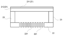
- FIGS. 2 to 4 are views showing a configuration example of the electrostatic drive device 2.
- the electrostatic drive device 2 includes a first electrode 21 and a second electrode 22.
- the first electrode 21 operates (vibrates) as a driving film, is a stack of a plurality of materials having different conductivitys, and is arranged by applying tension to a position facing the second electrode 22. It was set up. Specifically, in the first electrode 21, the first layer 211 and the second layer 212 are laminated, and the second layer 212 is arranged at a position facing the second electrode 22. The conductivity of the second layer 212 is lower than that of the first layer 211.
- the first layer 211 as a conductor and the second layer 212 as an insulator, it is possible to satisfy the condition that the conductivity of the second layer 212 is lower than that of the first layer 211. can. Further, the second layer 212 does not have to be an insulator and may be a conductor having a sufficiently high resistance value.
- the application of tension is to resonate at a desired resonance frequency and suppress the pull-in phenomenon.
- the pull-in phenomenon is a general problem in electrostatic actuators, and is a phenomenon in which the drive film sticks to the lower electrode and cannot operate. This is because the balance of the force applied to the vibrating membrane when the driving membrane is displaced, that is, the balance between the electrostatic force and the restoring force due to the membrane rigidity is lost.
- the parallel plate type structure is driven by a constant voltage, this phenomenon occurs when the displacement exceeds 1/3 of the initial gap. In a typical parallel plate type structure, the drive film is operated so as not to exceed this displacement.
- the second electrode 22 includes a through hole 221.
- the through hole 221 is for suppressing the reactance component due to the gas existing between the first electrode 21 and the second electrode 22. That is, in the through hole 221, when the first electrode 21 which is a driving film vibrates, the gas existing between the first electrode 21 and the second electrode 22 can freely enter and exit through the through hole 221. It is for doing so.
- At least one of the first electrode and the second electrode is a laminated film in which a plurality of materials having different conductivitys are laminated, but here, a case where the first electrode is a laminated film will be described. ..
- both the first electrode 21 and the second electrode 22 may be made of a laminated film.
- the first electrode 21 can be calibrated so that the first layer 213, the second layer 214, and the third layer 215 are laminated in this order.
- the third layer 215 is arranged at a position facing the second electrode 22.
- tension is applied to the first electrode 21.
- the first layer 213 and the third layer 215 are electrically connected to each other. This makes it possible to prevent the permanent charge from adhering to the surface of the second layer 214 when the electrostatic drive device 2 is operated.
- the second layer 214 is, for example, an insulator, and when an electric charge adheres to the insulator, the bias voltage due to the DC power supply 41 is effectively reduced.
- the conductivity of the second layer 214 is lower than that of the first layer 213, the conductivity of the third layer 215 is equal to or less than the conductivity of the first layer 213, and that of the second layer 214. Higher than conductivity.
- the first layer 213 is a first conductor
- the second layer 214 is an insulator
- the third layer 215 is a second conductor.
- first conductor first layer 213 and the second conductor (third layer 215) are connected via an electric resistance 216.
- electric resistance 216 Even when the first electrode 21 and the second electrode 22 come into contact with each other due to reasons such as the electrostatic drive device 2 being compressed when the electrostatic drive device 2 is operated, theoretically The short-circuit current that becomes infinite does not flow, only the current limited by the electric resistance 216 flows, and it is possible to prevent a large current from flowing through the electrostatic drive device 2.
- the electrical resistance 216 is connected, it is possible to prevent the permanent attachment of the charge to the surface of the second layer 214.
- the first layer 213 is used as the first conductor
- the second layer 214 is used as the insulator
- the third layer 215 is used as the second conductor
- the resistance value of the second conductor is the resistance of the first conductor.
- the second electrode 22 is configured such that the first conductor 222, the insulator 223, and the second conductor 224 are laminated in order, and the first conductor 222 and the second conductor 222 are laminated. It is also possible to electrically connect the conductor 224 to obtain the same effect.
- the second electrode 22 includes a through hole 221.
- the through hole 221 is for suppressing the reactance component due to the gas existing between the first electrode 21 and the second electrode 22. That is, in the through hole 221, when the first electrode 21 which is a driving film vibrates, the gas existing between the first electrode 21 and the second electrode 22 can freely enter and exit through the through hole 221. It is for doing so.
- the maximum distance between the first electrode 21 and the second electrode 22 is the value obtained by dividing the squared value of the discharge voltage at which a discharge occurs between the first electrode 21 and the second electrode 22 by the distance. Is a value that becomes.
- ⁇ is the dielectric constant of the gas between the first electrode 21 and the second electrode 22
- ⁇ is the conductor occupancy of the second electrode 22 having the through hole 221.
- the first electrode 21 and the second electrode 22 are filled with a gas having a property of being less likely to generate an electric discharge than air, for example, sulfur hexafluoride (SF 6 ). It is also possible to further suppress the discharge between the electrode 21 and the second electrode 22. As a result, the discharge voltage V can be increased, and as a result, the power upper limit value W can be increased.
- a gas having a property of being less likely to generate an electric discharge than air for example, sulfur hexafluoride (SF 6 ).
- the first electrode 21 is divided into units, and the size of each unit is set so that the resonance frequency of the first electrode 21 becomes a value corresponding to the drive frequency. Specifically, it is desirable that the size of each unit is determined so that the resonance frequency of the first electrode 21 is close to the drive frequency.
- the impedance matching layer 3 includes a matching film 31 and a gas 32.
- the impedance matching layer 3 is provided with a matching film 31 via a spacer 33 provided on the electrostatic drive device 2.
- the impedance matching layer 3 can also be used in combination with a drive device other than the electrostatic drive device 2.
- the matching film 31 is arranged by applying tension to a position facing the vibration surface of the vibration device, for example, the surface of the first electrode 21 which is the vibration film of the electrostatic drive device 2 on the side of the first layer 211. Will be done.
- the matching film 31 does not have an opening, and the vibrating surface also has no opening.
- the matching film 31 has a resonance loss of the same level as or less than the sound power transmitted.
- the real part of the mechanical impedance of the matching film 31 alone which represents the loss at resonance of the matching film 31 alone, is a value obtained by dividing the mass impedance of the matching film 31 by the Q value of the matching film 31 alone.
- the mechanical impedance of the matching film 31 alone is the ratio of the applied pressure to the vibration rate of the film when the matching film 31 is present alone, and the vibration rate and the applied pressure are the average values in the film. ..
- ⁇ / Q is an ultrasonic wave. Is equal to or less than the intrinsic acoustic impedance ⁇ c of the air to which the air is sent. Considering the electroacoustic conversion efficiency, it is desirable that ⁇ / Q is a value sufficiently smaller than ⁇ c.
- the gas 32 is enclosed between the matching film 31 and the vibration surface, for example, the surface of the first electrode 21, which is the vibration film of the electrostatic drive device 2, on the side of the first layer 211.
- the gas 32 is, for example, air.
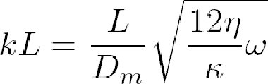
- the distance between the surface of the matching film 31 facing the vibrating surface and the vibrating surface, that is, the distance Dm between the matching film 31 and the vibrating surface depends on the amplitude amplification factor which is the ratio of the amplitude of the vibrating surface to the amplitude of the matching film. Will be decided. Specifically, when k is represented by the number 1, it is a condition of D m that the kL shown in the number 2 is 5 or less, and preferably, the kL is sufficiently smaller than 5 D.
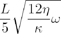
- the distance D m is equal to or greater than the first value shown in Equation 3.
- the condition of the distance D m described here is based on the viscous loss of the gas 32, and also indicates the condition in which the viscous loss does not matter. Therefore, although the distance D m is actually determined according to the amplitude amplification factor, it is necessary to determine the amplitude amplification factor so that the loss due to the viscosity and heat conduction determined by the distance D m is not excessive.
- the first value is a value obtained by multiplying the second value by the length L of the matching film 31 and divided by 5
- the second value is the square root of the third value.
- the third value is a value obtained by multiplying the value obtained by dividing the gas viscosity ⁇ of the gas by the gas bulk modulus ⁇ of the gas by 12, and further multiplying by the angular frequency ⁇ when the matching film 31 is vibrated.
- D m is a value sufficiently larger than 10 ⁇ m.
- the size L of the unit matching film 31 needs to be such that the lowest-order resonance frequency of a single unit of the matching film 31 is smaller than the frequency at which the matching film 31 is vibrated. This is because the reactance during driving of the matching film 31 alone is mass (inductive, reactance is a positive value). Therefore, the matching film 31, the first electrode 21, and the second electrode 22 have a predetermined size, and the unit fixed at the edge portion thereof is used as a unit, and these units are integrated in the plane direction to form an array. be able to.
- the unit has, for example, a matching film 31 or the like having a circular shape having a diameter of 2 mm.
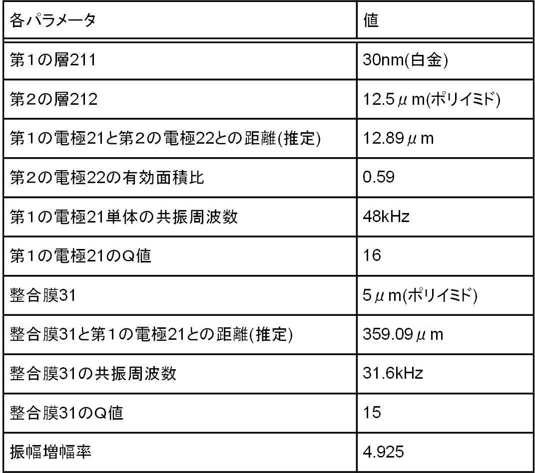
- the Q value of the first electrode 21 and the Q value of the matching film 31 in Table 1 are both measured in air.
- the amplitude amplification factor in Table 1 is the ratio of the amplitude of the matching film 31 to the amplitude of the driving film (first electrode 21).
- the present invention may be provided in each of the following embodiments. It is an impedance matching layer and includes a matching film and a gas.
- the matching film has an acoustic power or less at which a loss during resonance is transmitted, and tension is applied to a position facing the vibration surface of the vibrating device.
- the gas is disposed and is sealed between the matching film and the vibrating surface, and the distance between the matching film surface facing the vibrating surface and the vibrating surface is the amplitude of the vibrating surface and the vibration surface.
- An impedance matching layer that is a value corresponding to the amplitude amplification factor, which is the ratio of the amplitudes of the matching film.
- the distance is equal to or greater than the first value
- the first value is a value obtained by multiplying the second value by the length of the matching film and dividing by 5.
- the second value is the square root of the third value
- the third value is a value obtained by dividing the gas viscosity of the gas by the gas bulk modulus of the gas multiplied by 12, and further, the matching film.
- Impedance matching layer which is the value obtained by multiplying the angular frequency when vibrating.
- the matching film is an impedance matching layer having a magnitude such that the lowest-order resonance frequency of a single element of the matching film is smaller than the frequency at which the matching film is vibrated.
- the first electrode is a drive film, and tension is applied to a position facing the second electrode.
- the second electrode is provided with a through hole, and at least one of the first electrode and the second electrode is an electrostatic laminated film in which a plurality of materials having different conductivitys are laminated.
- Drive device In the electrostatic drive device, the laminated film is such that a first layer and a second layer are laminated, and the second layer is arranged at a position facing another electrode, and the second layer is formed.
- the conductivity of the electrostatic drive device is lower than the conductivity of the first layer.
- the laminated film is such that the first layer, the second layer, and the third layer are laminated in order, and the third layer is arranged at a position facing the other electrodes.
- the conductivity of the second layer is lower than that of the first layer, and the conductivity of the third layer is equal to or less than the conductivity of the first layer.
- An electrostatic drive device having a higher conductivity than the layer and in which the first layer and the third layer are electrically connected.
- the first layer is a first conductor
- the second layer is an insulator
- the third layer is a second conductor
- the second layer is a second conductor
- the resistance value of the conductor is higher than the resistance value of the first conductor.
- the first layer is a first conductor
- the second layer is an insulator
- the third layer is a second conductor
- the first layer is a first conductor
- the second layer is an insulator
- the third layer is a second conductor
- the first layer is an electrostatic drive device in which the conductor of the above and the second conductor are connected via an electric resistance.
- the first electrode is divided into units, and the size of the unit is such that the resonance frequency of the first electrode becomes a value corresponding to the drive frequency.
- Drive device In the electrostatic drive device, the distance between the first electrode and the second electrode is the square of the discharge voltage at which a discharge occurs between the first electrode and the second electrode.
- An electrostatic drive device whose maximum value is the value divided by the distance.
- an electrostatic drive device in which a gas having a property of being less likely to generate an electric discharge than air is filled between the first electrode and the second electrode. Of course, this is not the case.
- Ultrasonic device 2 Electrostatic drive device 3: Impedance matching layer 4: Power supply 5: Spacer 6: Substrate 21: First electrode 22: Second electrode 23: Spacer 31: Matching film 32: Gas 33: Spacer 41: DC power supply 42: AC power supply 211: First layer 212: Second layer 213: First layer 214: Second layer 215: Third layer 216: Electrical resistance 221: Through hole 222: First Conductor 223: Insulator 224: Second conductor
Landscapes
- Engineering & Computer Science (AREA)
- Physics & Mathematics (AREA)
- Computer Networks & Wireless Communication (AREA)
- General Physics & Mathematics (AREA)
- Radar, Positioning & Navigation (AREA)
- Remote Sensing (AREA)
- Acoustics & Sound (AREA)
- Signal Processing (AREA)
- Mechanical Engineering (AREA)
- Transducers For Ultrasonic Waves (AREA)
- Micromachines (AREA)
Abstract
Description
図1は、本発明の実施形態に係る超音波デバイスの構成例を示した図である。同図に示すように、超音波デバイス1は、静電駆動デバイス2と、インピーダンス整合層3と、電源4とを備える。この超音波デバイス1は、超音波を空気中等に送出するデバイスである。
図2乃至図4は、静電駆動デバイス2の構成例を示した図である。図2に示すように、静電駆動デバイス2は、第1の電極21と、第2の電極22とを備える。第1の電極21は、駆動膜として動作(振動)するもので、導電率の異なる複数の材料が積層されたものであり、第2の電極22と対向する位置に、張力が印加されて配設されたものである。具体的には、第1の電極21は、第1の層211と、第2の層212とが積層され、第2の層212が第2の電極22と対向する位置に配設される。第2の層212の導電率は、第1の層211の導電率よりも低い。例えば、第1の層211を導体とし、第2の層212を絶縁体とすることで、第2の層212の導電率が第1の層211の導電率よりも低いといった条件を満たすことができる。また、第2の層212は、絶縁体である必要はなく、十分に抵抗値の高い導体であってもよい。
図1に示すように、インピーダンス整合層3は、整合膜31と、気体32とを備える。インピーダンス整合層3は、静電駆動デバイス2の上に設けられたスペーサ33を介して整合膜31が設けられる。なお、インピーダンス整合層3は、静電駆動デバイス2以外の駆動デバイスと組み合わせて用いることも可能である。

整合膜31の大きさLは、整合膜31の単体の最低次共振周波数が、整合膜31を振動させる際の周波数より小さくなる大きさである必要がある。これは、整合膜31単体での駆動時リアクタンスが質量性(誘導性、リアクタンスが正の値)となるためである。このため、整合膜31、第1の電極21、第2の電極22を所定の大きさとし、これらの辺縁部で固定されたものをユニットとし、このユニットを平面方向に集積してアレイとすることができる。ユニットは、例えば、整合膜31等が、直径2mmの円形のものである。
表1に示すパラメータにより実験を行った。その結果、80kHzにおける目標振幅に、46.2kHzで到達し、インピーダンス整合層3によって所定の振幅増幅効果が得られることが確認できた。
本発明は、次に記載の各態様で提供されてもよい。
インピーダンス整合層であって、整合膜と、気体とを備え、前記整合膜は、共振時ロスが送出される音響パワー以下であり、振動デバイスの振動面に対向する位置に、張力が印加されて配設され、前記気体は、前記整合膜と前記振動面との間に封入され、前記振動面に対向する前記整合膜の面と、該振動面との距離が、前記振動面の振幅と前記整合膜の振幅の比である振幅増幅率に応じた値であるインピーダンス整合層。
前記インピーダンス整合層において、前記距離は、第1の値以上であり、前記第1の値は、第2の値に、前記整合膜の長さを乗じた値を5で除した値であり、前記第2の値は、第3の値の平方根であり、前記第3の値は、前記気体の気体粘性を前記気体の気体体積弾性率で除した値に12を乗じ、さらに、前記整合膜を振動させる際の角周波数を乗じた値であるインピーダンス整合層。
前記インピーダンス整合層において、前記整合膜は、該整合膜の単体の最低次共振周波数が、該整合膜を振動させる際の周波数より小さくなる大きさであるインピーダンス整合層。
静電駆動デバイスであって、第1の電極と、第2の電極とを備え、前記第1の電極は、駆動膜であり、前記第2の電極と対向する位置に、張力が印加されて配設され、前記第2の電極は、貫通孔を備え、前記第1の電極と前記第2の電極との少なくとも一方は、導電率の異なる複数の材料が積層された積層膜である静電駆動デバイス。
前記静電駆動デバイスにおいて、前記積層膜は、第1の層と、第2の層とが積層され、前記第2の層が他の電極と対向する位置に配設され、前記第2の層の導電率は、前記第1の層の導電率よりも低い静電駆動デバイス。
前記静電駆動デバイスにおいて、前記積層膜は、第1の層と、第2の層と、第3の層とが順に積層され、前記第3の層が他の電極と対向する位置に配設され、前記第2の層の導電率は、前記第1の層の導電率よりも低く、前記第3の層の導電率は、前記第1の層の導電率以下であり、前記第2の層の導電率よりも高く、前記第1の層と前記第3の層とが電気的に接続されている静電駆動デバイス。
前記静電駆動デバイスにおいて、前記第1の層は、第1の導体であり、前記第2の層は、絶縁体であり、前記第3の層は、第2の導体であり、前記第2の導体の抵抗値は、前記第1の導体の抵抗値よりも高い静電駆動デバイス。
前記静電駆動デバイスにおいて、前記第1の層は、第1の導体であり、前記第2の層は、絶縁体であり、前記第3の層は、第2の導体であり、前記第1の導体と前記第2の導体とが、電気抵抗を介して接続されている静電駆動デバイス。
前記静電駆動デバイスにおいて、前記第1の電極は、ユニットに区切られ、前記ユニットの大きさは、前記第1の電極の共振周波数が、駆動周波数に応じた値となる大きさである静電駆動デバイス。
前記静電駆動デバイスにおいて、前記第1の電極と前記第2の電極との距離は、前記第1の電極と前記第2の電極との間で放電が生じる放電電圧を2乗した値を前記距離で除した値が、最大となる値である静電駆動デバイス。
前記静電駆動デバイスにおいて、前記第1の電極と前記第2の電極との間に、空気よりも放電が生じにくい性質を有する気体が充満されている静電駆動デバイス。
もちろん、この限りではない。
2 :静電駆動デバイス
3 :インピーダンス整合層
4 :電源
5 :スペーサ
6 :基板
21 :第1の電極
22 :第2の電極
23 :スペーサ
31 :整合膜
32 :気体
33 :スペーサ
41 :直流電源
42 :交流電源
211 :第1の層
212 :第2の層
213 :第1の層
214 :第2の層
215 :第3の層
216 :電気抵抗
221 :貫通孔
222 :第1の導体
223 :絶縁体
224 :第2の導体
Claims (12)
- 超音波を送出する超音波デバイスであって、
静電駆動デバイスと、インピーダンス整合層とを備え、
前記静電駆動デバイスは、第1の電極と、第2の電極とを備え、
前記第1の電極は、駆動膜であり、前記第2の電極と対向する位置に、張力が印加されて配設され、
前記第2の電極は、貫通孔を備え、
前記第1の電極と前記第2の電極との少なくとも一方は、導電率の異なる複数の材料が積層された積層膜であり、
前記インピーダンス整合層は、整合膜と、気体とを備え、
前記整合膜は、
共振時ロスが送出される音響パワー以下であり、
前記第1の電極と対向する位置に、張力が印加されて配設され、
前記気体は、前記整合膜と前記第1の電極との間に封入され、
前記第1の電極に対向する前記整合膜の面と、対向する前記第1の電極の面との距離が、前記駆動膜の振幅と前記整合膜の振幅の比である振幅増幅率に応じた値である
超音波デバイス。 - インピーダンス整合層であって、
整合膜と、気体とを備え、
前記整合膜は、
共振時ロスが送出される音響パワー以下であり、
振動デバイスの振動面に対向する位置に、張力が印加されて配設され、
前記気体は、前記整合膜と前記振動面との間に封入され、
前記振動面に対向する前記整合膜の面と、該振動面との距離が、前記振動面の振幅と前記整合膜の振幅の比である振幅増幅率に応じた値である
インピーダンス整合層。 - 請求項2に記載のインピーダンス整合層において、
前記距離は、第1の値以上であり、
前記第1の値は、第2の値に、前記整合膜の長さを乗じた値を5で除した値であり、
前記第2の値は、第3の値の平方根であり、
前記第3の値は、前記気体の気体粘性を前記気体の気体体積弾性率で除した値に12を乗じ、さらに、前記整合膜を振動させる際の角周波数を乗じた値である
インピーダンス整合層。 - 請求項2又は請求項3に記載のインピーダンス整合層において、
前記整合膜は、該整合膜の単体の最低次共振周波数が、該整合膜を振動させる際の周波数より小さくなる大きさである
インピーダンス整合層。 - 静電駆動デバイスであって、
第1の電極と、第2の電極とを備え、
前記第1の電極は、駆動膜であり、前記第2の電極と対向する位置に、張力が印加されて配設され、
前記第2の電極は、貫通孔を備え、
前記第1の電極と前記第2の電極との少なくとも一方は、導電率の異なる複数の材料が積層された積層膜である
静電駆動デバイス。 - 請求項5に記載の静電駆動デバイスにおいて、
前記積層膜は、第1の層と、第2の層とが積層され、前記第2の層が他の電極と対向する位置に配設され、
前記第2の層の導電率は、前記第1の層の導電率よりも低い
静電駆動デバイス。 - 請求項5に記載の静電駆動デバイスにおいて、
前記積層膜は、第1の層と、第2の層と、第3の層とが順に積層され、前記第3の層が他の電極と対向する位置に配設され、
前記第2の層の導電率は、前記第1の層の導電率よりも低く、
前記第3の層の導電率は、前記第1の層の導電率以下であり、前記第2の層の導電率よりも高く、
前記第1の層と前記第3の層とが電気的に接続されている
静電駆動デバイス。 - 請求項7に記載の静電駆動デバイスにおいて、
前記第1の層は、第1の導体であり、
前記第2の層は、絶縁体であり、
前記第3の層は、第2の導体であり、
前記第2の導体の抵抗値は、前記第1の導体の抵抗値よりも高い
静電駆動デバイス。 - 請求項7に記載の静電駆動デバイスにおいて、
前記第1の層は、第1の導体であり、
前記第2の層は、絶縁体であり、
前記第3の層は、第2の導体であり、
前記第1の導体と前記第2の導体とが、電気抵抗を介して接続されている
静電駆動デバイス。 - 請求項5乃至請求項9のいずれか1項に記載の静電駆動デバイスにおいて、
前記第1の電極は、ユニットに区切られ、
前記ユニットの大きさは、前記第1の電極の共振周波数が、駆動周波数に応じた値となる大きさである
静電駆動デバイス。 - 請求項5乃至請求項10のいずれか1項に記載の静電駆動デバイスにおいて、
前記第1の電極と前記第2の電極との距離は、前記第1の電極と前記第2の電極との間で放電が生じる放電電圧を2乗した値を前記距離で除した値が、最大となる値である
静電駆動デバイス。 - 請求項5乃至請求項11のいずれか1項に記載の静電駆動デバイスにおいて、
前記第1の電極と前記第2の電極との間に、空気よりも放電が生じにくい性質を有する気体が充満されている
静電駆動デバイス。
Priority Applications (3)
| Application Number | Priority Date | Filing Date | Title |
|---|---|---|---|
| US18/270,342 US12601818B2 (en) | 2021-01-06 | 2021-12-23 | Ultrasound device, impedance matching layer, and electrostatic drive device |
| JP2022574003A JP7527680B2 (ja) | 2021-01-06 | 2021-12-23 | 超音波デバイス、インピーダンス整合層及び静電駆動デバイス |
| CN202180088959.3A CN116711327A (zh) | 2021-01-06 | 2021-12-23 | 超声波设备、阻抗匹配层及静电驱动设备 |
Applications Claiming Priority (2)
| Application Number | Priority Date | Filing Date | Title |
|---|---|---|---|
| JP2021-000922 | 2021-01-06 | ||
| JP2021000922 | 2021-01-06 |
Publications (1)
| Publication Number | Publication Date |
|---|---|
| WO2022149486A1 true WO2022149486A1 (ja) | 2022-07-14 |
Family
ID=82357301
Family Applications (1)
| Application Number | Title | Priority Date | Filing Date |
|---|---|---|---|
| PCT/JP2021/048057 Ceased WO2022149486A1 (ja) | 2021-01-06 | 2021-12-23 | 超音波デバイス、インピーダンス整合層及び静電駆動デバイス |
Country Status (4)
| Country | Link |
|---|---|
| US (1) | US12601818B2 (ja) |
| JP (1) | JP7527680B2 (ja) |
| CN (1) | CN116711327A (ja) |
| WO (1) | WO2022149486A1 (ja) |
Cited By (1)
| Publication number | Priority date | Publication date | Assignee | Title |
|---|---|---|---|---|
| WO2024202815A1 (ja) * | 2023-03-24 | 2024-10-03 | 国立大学法人 東京大学 | 超音波デバイス、制御装置、プログラム及びシステム |
Citations (3)
| Publication number | Priority date | Publication date | Assignee | Title |
|---|---|---|---|---|
| JPS5473618A (en) * | 1977-11-24 | 1979-06-13 | Sony Corp | Gas-filled condenser type speaker |
| JPH0523698U (ja) * | 1991-09-09 | 1993-03-26 | ホシデン株式会社 | エレクトレツトコンデンサマイクロホンユニツト |
| JP2014033301A (ja) * | 2012-08-02 | 2014-02-20 | Foster Electric Co Ltd | 接触型マイクロフォン |
Family Cites Families (17)
| Publication number | Priority date | Publication date | Assignee | Title |
|---|---|---|---|---|
| US5272758A (en) * | 1991-09-09 | 1993-12-21 | Hosiden Corporation | Electret condenser microphone unit |
| JP3345844B2 (ja) * | 1993-11-26 | 2002-11-18 | 日本特殊陶業株式会社 | 超音波送受波器 |
| JP3294496B2 (ja) * | 1996-04-16 | 2002-06-24 | 株式会社日立製作所 | 弾性表面波装置とそれを用いた通信装置 |
| CA2332158C (en) * | 2000-03-07 | 2004-09-14 | Matsushita Electric Industrial Co., Ltd. | Ultrasonic probe |
| JP2001346296A (ja) * | 2000-06-01 | 2001-12-14 | Matsushita Electric Ind Co Ltd | 音響整合部材とその製造方法 |
| JP4573483B2 (ja) * | 2001-09-20 | 2010-11-04 | 古野電気株式会社 | 超音波振動子 |
| WO2007017776A2 (en) * | 2005-08-08 | 2007-02-15 | Koninklijke Philips Electronics, N.V. | Wide-bandwidth matrix transducer with polyethylene third matching layer |
| JP2007104371A (ja) * | 2005-10-05 | 2007-04-19 | Seiko Epson Corp | 静電型超音波トランスデューサ |
| AU2010284313B2 (en) * | 2009-08-17 | 2016-01-28 | Histosonics, Inc. | Disposable acoustic coupling medium container |
| JP2011101163A (ja) * | 2009-11-05 | 2011-05-19 | Canon Inc | 静電容量型電気機械変換装置 |
| WO2011146138A2 (en) * | 2010-05-21 | 2011-11-24 | Misonix Incorporated | Dual-mode piezocomposite ultrasonic transducer |
| JP6707000B2 (ja) * | 2016-08-31 | 2020-06-10 | 国立大学法人 東京大学 | 超音波発生デバイス |
| JP2019029862A (ja) * | 2017-07-31 | 2019-02-21 | 国立大学法人 東京大学 | 超音波発生デバイス |
| GB201802593D0 (en) * | 2018-02-16 | 2018-04-04 | Fujifilm Diosynth Biotechnologies Uk Ltd | Rig |
| TWI791376B (zh) * | 2022-01-14 | 2023-02-01 | 佳世達科技股份有限公司 | 波形改善方法及超音波換能器 |
| JP2024137007A (ja) * | 2023-03-24 | 2024-10-04 | 国立大学法人 東京大学 | 超音波デバイス、制御装置、プログラム及びシステム |
| JP2025073618A (ja) * | 2023-10-27 | 2025-05-13 | アイリスオーヤマ株式会社 | 照明制御システム、照明装置、電子デバイス、照明制御方法、表示方法およびプログラム |
-
2021
- 2021-12-23 US US18/270,342 patent/US12601818B2/en active Active
- 2021-12-23 CN CN202180088959.3A patent/CN116711327A/zh active Pending
- 2021-12-23 JP JP2022574003A patent/JP7527680B2/ja active Active
- 2021-12-23 WO PCT/JP2021/048057 patent/WO2022149486A1/ja not_active Ceased
Patent Citations (3)
| Publication number | Priority date | Publication date | Assignee | Title |
|---|---|---|---|---|
| JPS5473618A (en) * | 1977-11-24 | 1979-06-13 | Sony Corp | Gas-filled condenser type speaker |
| JPH0523698U (ja) * | 1991-09-09 | 1993-03-26 | ホシデン株式会社 | エレクトレツトコンデンサマイクロホンユニツト |
| JP2014033301A (ja) * | 2012-08-02 | 2014-02-20 | Foster Electric Co Ltd | 接触型マイクロフォン |
Non-Patent Citations (1)
| Title |
|---|
| KAMIGAKI TAKAAKI, NINOMIYA YUKI, SHINODA HIROYUKI: "Electrostatically Driven Airborne Ultrasound Transducer with Perforated Backplate for Nonlinear Acoustic Applications", PROCEEDINGS OF THE 23RD INTERNATIONAL CONGRESS ON ACOUSTICS, DEUTSCHE GESELLSCHAFT FüR AKUSTIK, 13 September 2019 (2019-09-13), XP055949173, ISSN: 2226-7808, DOI: 10.18154/rwth-conv-238867 * |
Cited By (1)
| Publication number | Priority date | Publication date | Assignee | Title |
|---|---|---|---|---|
| WO2024202815A1 (ja) * | 2023-03-24 | 2024-10-03 | 国立大学法人 東京大学 | 超音波デバイス、制御装置、プログラム及びシステム |
Also Published As
| Publication number | Publication date |
|---|---|
| JP7527680B2 (ja) | 2024-08-05 |
| JPWO2022149486A1 (ja) | 2022-07-14 |
| CN116711327A (zh) | 2023-09-05 |
| US20240085544A1 (en) | 2024-03-14 |
| US12601818B2 (en) | 2026-04-14 |
Similar Documents
| Publication | Publication Date | Title |
|---|---|---|
| US8907733B2 (en) | Oscillator | |
| JP5682973B2 (ja) | 発振装置および電子機器 | |
| US9135906B2 (en) | Ultrasonic generator | |
| TWI589163B (zh) | 靜電式電聲傳導器 | |
| JPH09500247A (ja) | 高圧低インピーダンス静電トランスデューサ | |
| JP5803917B2 (ja) | 発振装置および電子機器 | |
| CN115567859B (zh) | 推挽式静电薄膜超声换能器及定向发声装置 | |
| JP7527680B2 (ja) | 超音波デバイス、インピーダンス整合層及び静電駆動デバイス | |
| JP5637211B2 (ja) | 発振装置 | |
| CN211240077U (zh) | 压电反馈模组及装置 | |
| JP5440422B2 (ja) | 発振装置 | |
| JP2012029078A (ja) | 発振装置 | |
| JP5810484B2 (ja) | 発振装置 | |
| JP2012029087A (ja) | 発振装置 | |
| JP5488266B2 (ja) | 発振装置 | |
| JP2019029862A (ja) | 超音波発生デバイス | |
| JP5516181B2 (ja) | 発振装置 | |
| CN223125012U (zh) | 一种mems压电执行器及扬声器 | |
| JP2012029104A (ja) | 発振装置および電子機器 | |
| JP2012217038A (ja) | 発振装置および携帯端末装置 | |
| JP2025170575A (ja) | 超音波トランスデューサおよび超音波センサ | |
| CN118321130A (zh) | 超声波换能器及电子设备 | |
| CN117376791A (zh) | 一种mems压电执行器及扬声器 | |
| JP2012015764A (ja) | 発振装置 | |
| JP2012134599A (ja) | 発振装置および電子機器 |
Legal Events
| Date | Code | Title | Description |
|---|---|---|---|
| 121 | Ep: the epo has been informed by wipo that ep was designated in this application |
Ref document number: 21917706 Country of ref document: EP Kind code of ref document: A1 |
|
| ENP | Entry into the national phase |
Ref document number: 2022574003 Country of ref document: JP Kind code of ref document: A |
|
| WWE | Wipo information: entry into national phase |
Ref document number: 18270342 Country of ref document: US |
|
| WWE | Wipo information: entry into national phase |
Ref document number: 202180088959.3 Country of ref document: CN |
|
| NENP | Non-entry into the national phase |
Ref country code: DE |
|
| 122 | Ep: pct application non-entry in european phase |
Ref document number: 21917706 Country of ref document: EP Kind code of ref document: A1 |
|
| WWG | Wipo information: grant in national office |
Ref document number: 18270342 Country of ref document: US |