WO2022145342A1 - 光変調器とそれを用いた光送信装置 - Google Patents
光変調器とそれを用いた光送信装置 Download PDFInfo
- Publication number
- WO2022145342A1 WO2022145342A1 PCT/JP2021/047930 JP2021047930W WO2022145342A1 WO 2022145342 A1 WO2022145342 A1 WO 2022145342A1 JP 2021047930 W JP2021047930 W JP 2021047930W WO 2022145342 A1 WO2022145342 A1 WO 2022145342A1
- Authority
- WO
- WIPO (PCT)
- Prior art keywords
- modulation
- electrode
- signal
- wiring
- optical
- Prior art date
- Legal status (The legal status is an assumption and is not a legal conclusion. Google has not performed a legal analysis and makes no representation as to the accuracy of the status listed.)
- Ceased
Links
Images




Classifications
-
- G—PHYSICS
- G02—OPTICS
- G02F—OPTICAL DEVICES OR ARRANGEMENTS FOR THE CONTROL OF LIGHT BY MODIFICATION OF THE OPTICAL PROPERTIES OF THE MEDIA OF THE ELEMENTS INVOLVED THEREIN; NON-LINEAR OPTICS; FREQUENCY-CHANGING OF LIGHT; OPTICAL LOGIC ELEMENTS; OPTICAL ANALOGUE/DIGITAL CONVERTERS
- G02F1/00—Devices or arrangements for the control of the intensity, colour, phase, polarisation or direction of light arriving from an independent light source, e.g. switching, gating or modulating; Non-linear optics
- G02F1/01—Devices or arrangements for the control of the intensity, colour, phase, polarisation or direction of light arriving from an independent light source, e.g. switching, gating or modulating; Non-linear optics for the control of the intensity, phase, polarisation or colour
- G02F1/21—Devices or arrangements for the control of the intensity, colour, phase, polarisation or direction of light arriving from an independent light source, e.g. switching, gating or modulating; Non-linear optics for the control of the intensity, phase, polarisation or colour by interference
- G02F1/212—Mach-Zehnder type
-
- G—PHYSICS
- G02—OPTICS
- G02F—OPTICAL DEVICES OR ARRANGEMENTS FOR THE CONTROL OF LIGHT BY MODIFICATION OF THE OPTICAL PROPERTIES OF THE MEDIA OF THE ELEMENTS INVOLVED THEREIN; NON-LINEAR OPTICS; FREQUENCY-CHANGING OF LIGHT; OPTICAL LOGIC ELEMENTS; OPTICAL ANALOGUE/DIGITAL CONVERTERS
- G02F1/00—Devices or arrangements for the control of the intensity, colour, phase, polarisation or direction of light arriving from an independent light source, e.g. switching, gating or modulating; Non-linear optics
- G02F1/01—Devices or arrangements for the control of the intensity, colour, phase, polarisation or direction of light arriving from an independent light source, e.g. switching, gating or modulating; Non-linear optics for the control of the intensity, phase, polarisation or colour
- G02F1/21—Devices or arrangements for the control of the intensity, colour, phase, polarisation or direction of light arriving from an independent light source, e.g. switching, gating or modulating; Non-linear optics for the control of the intensity, phase, polarisation or colour by interference
- G02F1/225—Devices or arrangements for the control of the intensity, colour, phase, polarisation or direction of light arriving from an independent light source, e.g. switching, gating or modulating; Non-linear optics for the control of the intensity, phase, polarisation or colour by interference in an optical waveguide structure
-
- G—PHYSICS
- G02—OPTICS
- G02B—OPTICAL ELEMENTS, SYSTEMS OR APPARATUS
- G02B6/00—Light guides; Structural details of arrangements comprising light guides and other optical elements, e.g. couplings
- G02B6/24—Coupling light guides
- G02B6/42—Coupling light guides with opto-electronic elements
- G02B6/4201—Packages, e.g. shape, construction, internal or external details
- G02B6/4274—Electrical aspects
- G02B6/4277—Protection against electromagnetic interference [EMI], e.g. shielding means
-
- G—PHYSICS
- G02—OPTICS
- G02F—OPTICAL DEVICES OR ARRANGEMENTS FOR THE CONTROL OF LIGHT BY MODIFICATION OF THE OPTICAL PROPERTIES OF THE MEDIA OF THE ELEMENTS INVOLVED THEREIN; NON-LINEAR OPTICS; FREQUENCY-CHANGING OF LIGHT; OPTICAL LOGIC ELEMENTS; OPTICAL ANALOGUE/DIGITAL CONVERTERS
- G02F1/00—Devices or arrangements for the control of the intensity, colour, phase, polarisation or direction of light arriving from an independent light source, e.g. switching, gating or modulating; Non-linear optics
- G02F1/01—Devices or arrangements for the control of the intensity, colour, phase, polarisation or direction of light arriving from an independent light source, e.g. switching, gating or modulating; Non-linear optics for the control of the intensity, phase, polarisation or colour
- G02F1/03—Devices or arrangements for the control of the intensity, colour, phase, polarisation or direction of light arriving from an independent light source, e.g. switching, gating or modulating; Non-linear optics for the control of the intensity, phase, polarisation or colour based on ceramics or electro-optical crystals, e.g. exhibiting Pockels effect or Kerr effect
- G02F1/035—Devices or arrangements for the control of the intensity, colour, phase, polarisation or direction of light arriving from an independent light source, e.g. switching, gating or modulating; Non-linear optics for the control of the intensity, phase, polarisation or colour based on ceramics or electro-optical crystals, e.g. exhibiting Pockels effect or Kerr effect in an optical waveguide structure
-
- G—PHYSICS
- G02—OPTICS
- G02F—OPTICAL DEVICES OR ARRANGEMENTS FOR THE CONTROL OF LIGHT BY MODIFICATION OF THE OPTICAL PROPERTIES OF THE MEDIA OF THE ELEMENTS INVOLVED THEREIN; NON-LINEAR OPTICS; FREQUENCY-CHANGING OF LIGHT; OPTICAL LOGIC ELEMENTS; OPTICAL ANALOGUE/DIGITAL CONVERTERS
- G02F1/00—Devices or arrangements for the control of the intensity, colour, phase, polarisation or direction of light arriving from an independent light source, e.g. switching, gating or modulating; Non-linear optics
- G02F1/01—Devices or arrangements for the control of the intensity, colour, phase, polarisation or direction of light arriving from an independent light source, e.g. switching, gating or modulating; Non-linear optics for the control of the intensity, phase, polarisation or colour
- G02F1/03—Devices or arrangements for the control of the intensity, colour, phase, polarisation or direction of light arriving from an independent light source, e.g. switching, gating or modulating; Non-linear optics for the control of the intensity, phase, polarisation or colour based on ceramics or electro-optical crystals, e.g. exhibiting Pockels effect or Kerr effect
- G02F1/035—Devices or arrangements for the control of the intensity, colour, phase, polarisation or direction of light arriving from an independent light source, e.g. switching, gating or modulating; Non-linear optics for the control of the intensity, phase, polarisation or colour based on ceramics or electro-optical crystals, e.g. exhibiting Pockels effect or Kerr effect in an optical waveguide structure
- G02F1/0356—Devices or arrangements for the control of the intensity, colour, phase, polarisation or direction of light arriving from an independent light source, e.g. switching, gating or modulating; Non-linear optics for the control of the intensity, phase, polarisation or colour based on ceramics or electro-optical crystals, e.g. exhibiting Pockels effect or Kerr effect in an optical waveguide structure controlled by a high-frequency electromagnetic wave component in an electric waveguide structure
-
- G—PHYSICS
- G02—OPTICS
- G02F—OPTICAL DEVICES OR ARRANGEMENTS FOR THE CONTROL OF LIGHT BY MODIFICATION OF THE OPTICAL PROPERTIES OF THE MEDIA OF THE ELEMENTS INVOLVED THEREIN; NON-LINEAR OPTICS; FREQUENCY-CHANGING OF LIGHT; OPTICAL LOGIC ELEMENTS; OPTICAL ANALOGUE/DIGITAL CONVERTERS
- G02F1/00—Devices or arrangements for the control of the intensity, colour, phase, polarisation or direction of light arriving from an independent light source, e.g. switching, gating or modulating; Non-linear optics
- G02F1/01—Devices or arrangements for the control of the intensity, colour, phase, polarisation or direction of light arriving from an independent light source, e.g. switching, gating or modulating; Non-linear optics for the control of the intensity, phase, polarisation or colour
- G02F1/21—Devices or arrangements for the control of the intensity, colour, phase, polarisation or direction of light arriving from an independent light source, e.g. switching, gating or modulating; Non-linear optics for the control of the intensity, phase, polarisation or colour by interference
- G02F1/225—Devices or arrangements for the control of the intensity, colour, phase, polarisation or direction of light arriving from an independent light source, e.g. switching, gating or modulating; Non-linear optics for the control of the intensity, phase, polarisation or colour by interference in an optical waveguide structure
- G02F1/2255—Devices or arrangements for the control of the intensity, colour, phase, polarisation or direction of light arriving from an independent light source, e.g. switching, gating or modulating; Non-linear optics for the control of the intensity, phase, polarisation or colour by interference in an optical waveguide structure controlled by a high-frequency electromagnetic component in an electric waveguide structure
Definitions
- the present invention relates to an optical modulator and an optical transmission device using the same, and in particular, is applied to a modulation substrate having an optical waveguide and a modulation electrode for modulating a light wave propagating in the optical waveguide, and a modulation electrode.
- the present invention relates to an optical modulator provided with a wiring board provided with wiring for relaying a modulation signal.
- an optical modulator using a modulation substrate having an optical waveguide and a modulation electrode that modulates a light wave propagating in the optical waveguide is widely used.
- optical modulators are required to have a wider band or smaller size, and a plurality of different high-frequency signals are simultaneously applied to one optical modulator.
- Patent Document 1 proposes a structure in which a wiring board is arranged so as to overlap the modulation board.
- the problem to be solved by the present invention is to solve the above-mentioned problems and to provide an optical modulator capable of suppressing crosstalk of a modulated signal even when a wiring board is arranged so as to overlap the modulation board. be.
- Another object of the present invention is to provide an optical transmission device using these light modulators.
- the light modulator and the optical transmitter of the present invention have the following technical features.
- a modulation substrate having an optical waveguide and a modulation electrode for modulating a light wave propagating in the optical waveguide, and a wiring board provided with a wiring for relaying a modulation signal applied to the modulation electrode.
- the wiring board is arranged so as to overlap the modulation board so as to cover the action part where the modulation is performed by the modulation electrode, and the wiring board has at least a part of the position facing the action part. It is characterized in that a radio wave absorbing member is arranged therein.
- the radio wave absorbing member is characterized in that it is connected to either the grounded wiring of the wiring board or the grounded electrode of the modulation electrode.
- a plurality of Mach-Zehnder-type optical waveguides are arranged in parallel in the working portion, and a modulation electrode is provided corresponding to each Mach-Zehnder-type optical waveguide. It is characterized by being arranged.
- the modulation electrode includes a signal electrode and a ground electrode arranged so as to sandwich the signal electrode, and the signal electrode and the radio wave absorbing member.
- the distance to the signal electrode is larger than the distance between the signal electrode and the ground electrode.
- the modulation electrode is composed of a signal electrode and a ground electrode, and is located between a specific Mach Zender type optical waveguide and an adjacent Mach Zender type optical waveguide.
- the ground electrode and the radio wave absorbing member are arranged so as to face each other.
- the radio wave absorbing member is arranged inside the grounding electrode, and the side surfaces of both are arranged.
- the distance S is characterized in that the following equation is satisfied by using the width W of the signal electrode adjacent to the ground electrode and the distance G between the signal electrode and the ground electrode. S ⁇ 2G + W ⁇ ⁇ ⁇ ⁇ Expression
- the radio wave absorbing member extends along the signal electrode to the outside of the acting portion.
- a terminating device electrically connected to the modulation electrode is arranged on the wiring board. ..
- a driver circuit element that generates a modulation signal applied to the modulation electrode is arranged adjacent to the modulation substrate, and the driver circuit is provided.
- the output terminal of the element is characterized in that it is connected to the wiring of the wiring board.
- An optical transmitter comprising the optical modulator according to any one of (1) to (9) above and a signal generator for generating a modulation signal to be input to the driver circuit element. ..
- a modulation board having an optical waveguide and a modulation electrode for modulating a light wave propagating in the optical waveguide, and a wiring board provided with a wiring for relaying a modulation signal applied to the modulation electrode are provided.
- the wiring board is arranged so as to overlap the modulation board so as to cover the action part where the modulation is performed by the modulation electrode, and the wiring board has a radio wave at a position facing the action part. Since the absorbing member is arranged, it is possible to provide an optical modulator capable of effectively suppressing crosstalk of the modulated signal even when the wiring substrate is arranged so as to overlap the modulation substrate.
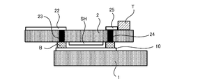
- the present invention comprises a modulation substrate 1 having an optical waveguide and a modulation electrode 10 for modulating a light wave propagating in the optical waveguide, and a modulation signal applied to the modulation electrode 10.
- the wiring board is arranged so as to cover an action portion where modulation is performed by the modulation electrode, and is arranged so as to be superimposed on the modulation board.
- the substrate is characterized in that the radio wave absorbing member SH is arranged at least a part of the position facing the acting portion.
- FIG. 1 is a plan view showing an example of an optical modulator.
- the mainstream is to introduce the input light to one end face of the optical modulator and derive the output light from the other end face, but in recent years, as shown in FIG. 1, one side of the optical modulator (FIG.
- the input collimator 6 for introducing the input light L1 and the output collimator 60 for deriving the output light L2 are both arranged on the right side of the above) to facilitate the connection related to the optical signal.
- An optical waveguide is formed on the modulation substrate 1, an input light L1 is incident on the modulation substrate 1, and a light wave related to the output light L2 is output.
- an input terminal 4 for inputting the modulation signal Sin is provided on the side opposite to the input / output unit of the light wave.
- the input terminal 4 is composed of flexible wiring, a connector terminal, or the like.
- the modulated signal Sin is generated by a digital signal processor (DSP) or the like arranged outside the housing.
- DSP digital signal processor
- the modulation signal Sin input from the input terminal 4 is input to the driver circuit element 3 via the circuit board 40.
- the driver circuit element 3 has signal amplifiers connected in multiple stages and outputs an amplified modulated signal.
- the modulation signal output by the driver circuit element 3 is applied to the modulation electrode of the modulation board 1 via the wiring board 2.
- the driver circuit element 3 may be housed in the housing 5 like the modulation board 1, but can also be arranged outside the housing 5. Further, reference numeral 50 indicates a lid member for airtightly sealing the housing 5.
- a ferroelectric substrate having an electro-optical effect such as lithium niobate (LN), lithium tantalate (LT), or PLZT (lead lanthanum tantalate zirconate), or a reinforced substrate made of these materials is used. Those with a phase growth film formed are available. Further, a substrate using various materials such as a semiconductor material such as InP or an organic material can also be used.
- a rib-type optical waveguide having a convex portion corresponding to the optical waveguide is used on the substrate, such as etching the surface of a substrate other than the optical waveguide or forming grooves on both sides of the optical waveguide. It is possible. It is also possible to form an optical waveguide by forming a high refractive index portion on the surface of the substrate by a thermal diffusion method, a proton exchange method, or the like for Ti or the like. It is also possible to form a composite optical waveguide by diffusing a high-refractive index material in the rib-type optical waveguide portion.
- the thickness of the modulation substrate on which the optical waveguide is formed may be composed of a thin plate of 10 ⁇ m or less, more preferably 5 ⁇ m or less, in order to achieve speed matching between the microwave and the light wave of the modulation signal.
- the height of the rib-type optical waveguide is set to 2 ⁇ m or less, more preferably 1 ⁇ m or less. It is also possible to form a vapor phase growth film on the reinforcing substrate and process the film into the shape of an optical waveguide.
- the modulation board composed of thin plates is bonded and fixed to the reinforcing board via direct bonding or an adhesive layer such as resin in order to increase the mechanical strength.
- an adhesive layer such as resin
- a material having a lower refractive index than the optical waveguide or a substrate on which the optical waveguide is formed and having a thermal expansion coefficient close to that of the optical waveguide or the like, for example, quartz or the like is preferably used.
- the same material as the thin plate such as the LN substrate as the reinforcing substrate.
- a modulation electrode or a bias electrode is formed along the optical wave guide.
- the electrode can be formed by laminating Au on a base metal such as Au or Ti by a plating method.
- FIG. 2 is an enlarged view of the dotted frame portion of FIG. 1 (b), and the wiring 22 (25) for propagating the modulation signal is formed on the wiring board 2.
- the wiring board 2 an insulating substrate using a ceramic of alumina or aluminum nitride is used, and electrical wiring is formed on the upper surface or the lower surface of the wiring board 2 of FIG. Further, a terminating device T for a modulation signal is also formed on the wiring board 2.
- Vias 23 and 24 are provided on the wiring board 2, and wiring is connected to the opposite surface of the board.
- the connection between the wiring board (connection wiring portion (pad portion) formed on the back surface of the wiring board) and the modulation electrode 10 of the modulation board 1 is performed by flip-chip bond. Specifically, there is a method of forming a pad portion of a wiring substrate with an Au electrode pad and connecting it to an Au electrode of a modulation electrode by crimping by applying heat / vibration, or a bump connection using a conductive adhesive B.
- the modulation signal is introduced from the wiring 22 through the via 23 and the bump B to the modulation electrode 10. After that, it reaches the wiring 25 through the bump and the via 24, and reaches the terminating device T composed of the terminating resistor and the like. Since the terminating member T serves as a heat source, it may be kept as far away from the substrate 1 as possible.
- the feature of the optical modulator of the present invention is that the radio wave absorbing member SH is arranged at a position facing the modulation substrate 1 (the working portion of the modulation electrode 10) of the wiring board 2.
- the radio wave absorbing member may be made of a ferrite sintered material using iron, carbon, nickel, Kovar or the like.
- the radio wave absorbing member may be connected to either the ground wiring of the wiring formed on the wiring board 2 or the ground electrode (a part of the modulation electrode) of the modulation electrode 1 and set to the ground potential.
- FIGS. 3 to 9 show an example of using two nested optical waveguides for the optical waveguide.
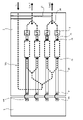
- FIG. 3 shows a wiring board 2, and an optical waveguide formed on another modulation board is shown by a dotted line WG.
- Reference numeral 3 is a driver circuit element, and the modulation signal is transmitted from the output terminal 30 formed on the upper surface to the pad portion 21 of the wiring of the wiring board 2 via the wire bonding WB. The modulated signal is guided from the pad portion 21 to the back surface of the wiring board 2 via the wiring 22 and the via 23.
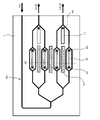
- FIG. 4 is a plan view of the modulation substrate 1.
- An optical waveguide WG, a modulation electrode 10, and a bias electrode 11 are formed on the modulation substrate 1.
- the description of the ground electrode and the like formed so as to sandwich the modulation electrode is omitted.
- the modulation signal that has passed through the modulation electrode 10 propagates to the wiring 240 of the wiring board 2 via the bump connection B2, and further reaches the terminating device T via the via 24 and the wiring 25.
- the terminating device T has a circuit configuration in which a terminating resistor and the like are combined, and the modulated signal is converted into heat energy and becomes a heat source.
- the wiring board 2 is hermetically sealed in the metal housing 5 together with the modulation board 1, so that the terminator T is moved away from the action portion of the modulation board 1, particularly the modulation electrode 10. It may be arranged.
- a bias electrode 11 is formed on the modulation substrate 1 in order to control the bias voltage of optical modulation.
- the voltage supply to the bias electrode 11 is also the wiring 27, via 28, and wiring of the wiring board 2 of FIGS. 3 and 5. It is also possible to carry out via 280 and the bump connection B3.
- a plurality of Mach-Zehnder-type optical waveguides are arranged in parallel in the acting portion where the modulation electrode 10 applies an electric field to the optical waveguide.
- a modulation electrode is arranged corresponding to each Mach-Zehnder type optical waveguide. Different modulation signals are applied to each modulation electrode 10, and crosstalk also occurs with each other.
- the radio wave absorbing member SH is arranged on the wiring board 2 corresponding to the acting portion of the modulation electrode 10. The radio wave absorbing member SH suppresses a part of the modulation signal leaking from the wiring board 2 side from being mixed in the modulation electrode 10.
- the radio wave absorbing member SH is formed on the surface of the wiring board 2, a recess may be formed in the wiring board 2 and may be formed so as to be embedded in the recess, if necessary.
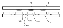
- FIGS. 6 (a) to 6 (c) A part of each cross-sectional view taken along the dotted lines A1 to A3 in FIG. 5 is shown in FIGS. 6 (a) to 6 (c).
- the reference numerals WG1 and WG2 drawn in FIGS. 6 (b) and 6 (c) indicate a branch waveguide of one Mach-Zehnder type optical waveguide of the optical waveguide WG.
- the modulation electrode includes a signal electrode 10 and a ground electrode GND arranged so as to sandwich the signal electrode 10, and the distance H between the signal electrode 10 and the radio wave absorbing member SH is the signal. It is set to be larger than the distance G between the electrode 10 and the ground electrode GND. This is to prevent the presence of the radio wave absorbing member from obstructing the electric field formed between the signal electrode and the ground electrode.
- FIG. 6 an embodiment in which the radio wave absorbing member SH is arranged above the signal electrode is shown.
- a part of the electric field formed by the signal electrode and the ground electrode is absorbed by the radio wave absorbing member and branches.
- the electric fields applied to the waveguides WG1 and WG2 may be weakened.
- FIGS. 7 to 9 describe an embodiment in which the radio wave absorbing member is arranged so as to face the ground electrode arranged between the signal electrodes 10.
- FIG. 7 is a diagram in which the arrangement pattern of the radio wave absorbing member SH arranged on the wiring board 2 is superimposed on the modulation board 1 of FIG.
- the radio wave absorbing member SH is arranged between the adjacent Mach-Zehnder type optical waveguides or between the signal electrodes.
- FIG. 8 is a cross-sectional view taken along the dotted line A3 of FIG.
- a ground electrode GND is arranged between adjacent Mach Zender type optical waveguides (between signal electrodes), and a radio wave absorbing member SH is arranged on the wiring board 2 so as to face the ground electrode.
- the radio wave absorbing member SH and the ground electrode GND effectively suppress crosstalk of the modulated signal applied to the acting portion of the adjacent Mach-Zehnder type optical waveguide.
- the radio wave absorbing member SH is not arranged on the upper side of the signal electrode, absorption of the electric field formed by the signal electrode is also suppressed.
- FIG. 9 is a further enlarged view of a part of FIG.
- a bump B that electrically connects the ground electrode GND and the ground wiring provided on the wiring board 2 is also shown.
- the height H of the bump B is about 50 ⁇ m.
- the radio wave absorbing member SH in FIG. 9 When the ground electrode GND and the radio wave absorbing member SH in FIG. 9 are viewed in a plan view from above the drawing, the radio wave absorbing member SH is arranged inside the ground electrode GND. Further, the distance S between the two sides is set so as not to affect the electric field formed by the signal electrode 10 (SIG1 or SIG2) as much as possible. Specifically, the width W of the signal electrode adjacent to the ground electrode and the distance G between the signal electrode and the ground electrode are set so as to satisfy the following equation. S ⁇ 2G + W ⁇ ⁇ ⁇ ⁇ Expression
- the length in the direction in which the modulated signal of the radio wave absorbing member SH propagates is extended to the outside of the acting portion of the signal electrode 10, thereby extending the wiring substrate. It is possible to effectively block the cross talk signal radiated from the bump connection B1 which is the connection portion between the wiring 230 formed on the back surface of No. 2 and the modulation electrode 10 of the modulation substrate 1.
- the region of the action portion (horizontal width in the drawing) in FIG. 7 substantially coincides with the length of the signal electrode 10.
- the length of the radio wave shielding member SH is longer than the length of the signal electrode 10.
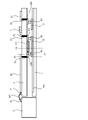
- FIG. 10 is a modification of FIG. 5, and wiring 22 and the like are provided on the back surface of the wiring board 2. Then, a driver circuit element 3 which is arranged adjacent to the modulation board 1 and generates a modulation signal applied to the modulation electrode 10 is arranged, and the wiring board 2 is arranged at an output terminal formed on the upper surface of the driver circuit element. The wiring 22 is connected. As a result, the wire bonding WB of FIG. 5 is also omitted, and wiring can be simplified.
- the terminating member T is provided on the lower surface of the wiring board 2, but it goes without saying that it can be arranged on the upper surface of the wiring board 2 as in FIG.
- optical modulator By including the above-mentioned optical modulator and a signal generator that generates a modulation signal to be input to the driver circuit element in the optical modulator, it is possible to provide an optical transmitter having the same effect.
- an optical modulator capable of suppressing crosstalk of a modulated signal even when the wiring board is arranged so as to overlap the modulation substrate. It is also possible to provide an optical transmission device using these light modulators.
Landscapes
- Physics & Mathematics (AREA)
- Nonlinear Science (AREA)
- General Physics & Mathematics (AREA)
- Optics & Photonics (AREA)
- Electromagnetism (AREA)
- Chemical & Material Sciences (AREA)
- Engineering & Computer Science (AREA)
- Ceramic Engineering (AREA)
- Crystallography & Structural Chemistry (AREA)
- Optical Modulation, Optical Deflection, Nonlinear Optics, Optical Demodulation, Optical Logic Elements (AREA)
Abstract
Description
(1) 光導波路と該光導波路を伝搬する光波を変調するための変調電極とを有する変調基板と、該変調電極に印加される変調信号を中継する配線を設けた配線基板とを備えた光変調器において、該配線基板は、該変調電極により変調が行われる作用部を覆うように、該変調基板に重ねて配置され、該配線基板には、該作用部に対向する位置の少なくとも一部に、電波吸収部材が配置されていることを特徴とする。
S≧2G+W ・・・・ 式
本発明は、図1乃至10に示すように、光導波路と該光導波路を伝搬する光波を変調するための変調電極10とを有する変調基板1と、該変調電極10に印加される変調信号を中継する配線22を設けた配線基板2とを備えた光変調器において、該配線基板は、該変調電極により変調が行われる作用部を覆うように、該変調基板に重ねて配置され、該配線基板には、該作用部に対向する位置の少なくとも一部に、電波吸収部材SHが配置されていることを特徴とする。
また、InPなどの半導体材料又は有機材料など種々の材料を利用した基板も利用可能である。
S≧2G+W ・・・・ 式
2 配線基板
3 ドライバ回路素子
SH 電波吸収部材
Claims (10)
- 光導波路と該光導波路を伝搬する光波を変調するための変調電極とを有する変調基板と、
該変調電極に印加される変調信号を中継する配線を設けた配線基板とを備えた光変調器において、
該配線基板は、該変調電極により変調が行われる作用部を覆うように、該変調基板に重ねて配置され、
該配線基板には、該作用部に対向する位置の少なくとも一部に、電波吸収部材が配置されていることを特徴とする光変調器。 - 請求項1に記載の光変調器において、該電波吸収部材は、該配線基板の接地配線又は該変調電極の接地電極のいずれかに接続されていることを特徴とする光変調器。
- 請求項1又は2に記載の光変調器において、該作用部では、複数のマッハツェンダー型光導波路が並列に配置され、各マッハツェンダー型光導波路に対応して変調電極が配置されていることを特徴とする光変調器。
- 請求項1乃至3のいずれかに記載の光変調器において、該変調電極は信号電極とそれを挟むように配置される接地電極を備え、該信号電極と該電波吸収部材までの距離は、該信号電極と該接地電極との間隔よりも大きいことを特徴とする光変調器。
- 請求項3に記載の光変調器において、該変調電極は信号電極と接地電極で構成され、特定のマッハツェンダー型光導波路と隣接する他のマッハツェンダー型光導波路との間に、該接地電極と該電波吸収部材とを対向して配置することを特徴とする光変調器。
- 請求項5に記載の光変調器において、該接地電極と該電波吸収部材とを平面視した場合に、該接地電極の内側に該電波吸収部材が配置され、両者の側辺の距離Sは、該接地電極に隣接する該信号電極の幅Wと該信号電極と該接地電極との間隔Gを用いて、以下の式を満足することを特徴とする光変調器。
S≧2G+W ・・・・ 式 - 請求項5又は6に記載の光変調器において、該電波吸収部材は、該信号電極に沿って、該作用部の外にまで延びていることを特徴とする光変調器。
- 請求項1乃至7のいずれかに記載の光変調器において、該配線基板には、該変調電極と電気的に接続される終端器が配置されていることを特徴とする光変調器。
- 請求項1乃至8のいずれかに記載の光変調器において、該変調基板に隣接して該変調電極に印加する変調信号を発生するドライバ回路素子が配置され、該ドライバ回路素子の出力端子は、該配線基板の配線に接続されていることを特徴とする光変調器。
- 請求項1乃至9のいずれかに記載の光変調器と、該ドライバ回路素子に入力する変調信号を生成する信号発生器とを備えることを特徴とする光送信装置。
Priority Applications (2)
| Application Number | Priority Date | Filing Date | Title |
|---|---|---|---|
| US18/267,695 US12474619B2 (en) | 2020-12-28 | 2021-12-23 | Optical modulator and optical transmission device using same |
| CN202180084162.6A CN116762036A (zh) | 2020-12-28 | 2021-12-23 | 光调制器和使用了该光调制器的光发送装置 |
Applications Claiming Priority (2)
| Application Number | Priority Date | Filing Date | Title |
|---|---|---|---|
| JP2020219102A JP7567471B2 (ja) | 2020-12-28 | 2020-12-28 | 光変調器とそれを用いた光送信装置 |
| JP2020-219102 | 2020-12-28 |
Publications (1)
| Publication Number | Publication Date |
|---|---|
| WO2022145342A1 true WO2022145342A1 (ja) | 2022-07-07 |
Family
ID=82259374
Family Applications (1)
| Application Number | Title | Priority Date | Filing Date |
|---|---|---|---|
| PCT/JP2021/047930 Ceased WO2022145342A1 (ja) | 2020-12-28 | 2021-12-23 | 光変調器とそれを用いた光送信装置 |
Country Status (4)
| Country | Link |
|---|---|
| US (1) | US12474619B2 (ja) |
| JP (1) | JP7567471B2 (ja) |
| CN (1) | CN116762036A (ja) |
| WO (1) | WO2022145342A1 (ja) |
Cited By (2)
| Publication number | Priority date | Publication date | Assignee | Title |
|---|---|---|---|---|
| WO2025186938A1 (ja) * | 2024-03-06 | 2025-09-12 | 住友大阪セメント株式会社 | 光導波路素子及びそれを用いた光変調器並びに光送信装置 |
| GB2639539A (en) * | 2024-02-21 | 2025-10-01 | Cambridge Consultants | Optical modulation |
Families Citing this family (1)
| Publication number | Priority date | Publication date | Assignee | Title |
|---|---|---|---|---|
| JPWO2025004256A1 (ja) * | 2023-06-28 | 2025-01-02 |
Citations (6)
| Publication number | Priority date | Publication date | Assignee | Title |
|---|---|---|---|---|
| JPH10239647A (ja) * | 1997-02-28 | 1998-09-11 | Tdk Corp | 光変調器 |
| JP2001174766A (ja) * | 1999-12-21 | 2001-06-29 | Sumitomo Osaka Cement Co Ltd | 導波路型光変調器 |
| JP2016071199A (ja) * | 2014-09-30 | 2016-05-09 | 住友大阪セメント株式会社 | 光制御素子 |
| US20180102847A1 (en) * | 2016-10-11 | 2018-04-12 | Korea Advanced Institute Of Science And Technology | Photonic beam forming network chip based on silicon semiconductor |
| WO2019239683A1 (ja) * | 2018-06-14 | 2019-12-19 | 三菱電機株式会社 | 光変調器及び光送信モジュール |
| WO2020202607A1 (ja) * | 2019-03-29 | 2020-10-08 | 住友大阪セメント株式会社 | 光変調素子、及び光変調モジュール |
Family Cites Families (5)
| Publication number | Priority date | Publication date | Assignee | Title |
|---|---|---|---|---|
| US5042895A (en) * | 1988-01-19 | 1991-08-27 | E. I. Du Pont De Nemours And Company | Waveguide structure using potassium titanyl phosphate |
| EP2653908A1 (en) * | 2012-04-16 | 2013-10-23 | Leica Geosystems AG | Electro-optic modulator and electro-optic distance-measuring device |
| JP6221294B2 (ja) | 2013-03-28 | 2017-11-01 | 住友大阪セメント株式会社 | 光制御素子 |
| JP6229649B2 (ja) * | 2014-12-08 | 2017-11-15 | 富士通オプティカルコンポーネンツ株式会社 | 光モジュール |
| JP6627379B2 (ja) * | 2015-09-30 | 2020-01-08 | 住友大阪セメント株式会社 | 光制御素子 |
-
2020
- 2020-12-28 JP JP2020219102A patent/JP7567471B2/ja active Active
-
2021
- 2021-12-23 CN CN202180084162.6A patent/CN116762036A/zh active Pending
- 2021-12-23 WO PCT/JP2021/047930 patent/WO2022145342A1/ja not_active Ceased
- 2021-12-23 US US18/267,695 patent/US12474619B2/en active Active
Patent Citations (6)
| Publication number | Priority date | Publication date | Assignee | Title |
|---|---|---|---|---|
| JPH10239647A (ja) * | 1997-02-28 | 1998-09-11 | Tdk Corp | 光変調器 |
| JP2001174766A (ja) * | 1999-12-21 | 2001-06-29 | Sumitomo Osaka Cement Co Ltd | 導波路型光変調器 |
| JP2016071199A (ja) * | 2014-09-30 | 2016-05-09 | 住友大阪セメント株式会社 | 光制御素子 |
| US20180102847A1 (en) * | 2016-10-11 | 2018-04-12 | Korea Advanced Institute Of Science And Technology | Photonic beam forming network chip based on silicon semiconductor |
| WO2019239683A1 (ja) * | 2018-06-14 | 2019-12-19 | 三菱電機株式会社 | 光変調器及び光送信モジュール |
| WO2020202607A1 (ja) * | 2019-03-29 | 2020-10-08 | 住友大阪セメント株式会社 | 光変調素子、及び光変調モジュール |
Cited By (2)
| Publication number | Priority date | Publication date | Assignee | Title |
|---|---|---|---|---|
| GB2639539A (en) * | 2024-02-21 | 2025-10-01 | Cambridge Consultants | Optical modulation |
| WO2025186938A1 (ja) * | 2024-03-06 | 2025-09-12 | 住友大阪セメント株式会社 | 光導波路素子及びそれを用いた光変調器並びに光送信装置 |
Also Published As
| Publication number | Publication date |
|---|---|
| CN116762036A (zh) | 2023-09-15 |
| JP7567471B2 (ja) | 2024-10-16 |
| US20240061309A1 (en) | 2024-02-22 |
| JP2022104096A (ja) | 2022-07-08 |
| US12474619B2 (en) | 2025-11-18 |
Similar Documents
| Publication | Publication Date | Title |
|---|---|---|
| WO2022145342A1 (ja) | 光変調器とそれを用いた光送信装置 | |
| US8031987B2 (en) | Optical modulator | |
| JP2020166159A (ja) | 光導波路素子、及び光導波路デバイス | |
| US12591152B2 (en) | Optical modulator and optical transmission device using same | |
| US11442329B2 (en) | Optical waveguide element, optical modulator, optical modulation module, and optical transmission apparatus | |
| WO2020115999A1 (ja) | 光変調器 | |
| CN116249930B (zh) | 光调制器及使用其的光发送装置 | |
| JP4056545B2 (ja) | 高周波線路の接続構造 | |
| WO2023188366A1 (ja) | 光デバイスとそれを用いた光送信装置 | |
| JP7035704B2 (ja) | 光導波路素子 | |
| JP7098930B2 (ja) | 光変調器及びそれを用いた光送信装置 | |
| JP6729133B2 (ja) | 光変調器 | |
| US20250355310A1 (en) | Optical waveguide element, and optical transmission apparatus and optical modulation device using optical waveguide element | |
| JP7677102B2 (ja) | 光導波路素子及びそれを用いた光変調デバイス並びに光送信装置 | |
| US20250264746A1 (en) | Optical modulation device, optical modulator, optical modulation module, optical transmission apparatus, and optical transmission system | |
| JP3824265B2 (ja) | 高周波線路の接続構造 | |
| WO2024247269A1 (ja) | 光回路 | |
| WO2024247268A1 (ja) | 光回路 | |
| WO2025186938A1 (ja) | 光導波路素子及びそれを用いた光変調器並びに光送信装置 |
Legal Events
| Date | Code | Title | Description |
|---|---|---|---|
| 121 | Ep: the epo has been informed by wipo that ep was designated in this application |
Ref document number: 21915202 Country of ref document: EP Kind code of ref document: A1 |
|
| WWE | Wipo information: entry into national phase |
Ref document number: 202180084162.6 Country of ref document: CN |
|
| NENP | Non-entry into the national phase |
Ref country code: DE |
|
| 122 | Ep: pct application non-entry in european phase |
Ref document number: 21915202 Country of ref document: EP Kind code of ref document: A1 |
|
| WWG | Wipo information: grant in national office |
Ref document number: 18267695 Country of ref document: US |