WO2022137702A1 - 半導体装置及び電子機器 - Google Patents
半導体装置及び電子機器 Download PDFInfo
- Publication number
- WO2022137702A1 WO2022137702A1 PCT/JP2021/035901 JP2021035901W WO2022137702A1 WO 2022137702 A1 WO2022137702 A1 WO 2022137702A1 JP 2021035901 W JP2021035901 W JP 2021035901W WO 2022137702 A1 WO2022137702 A1 WO 2022137702A1
- Authority
- WO
- WIPO (PCT)
- Prior art keywords
- base
- tubular member
- semiconductor device
- housing
- plan
- Prior art date
- Legal status (The legal status is an assumption and is not a legal conclusion. Google has not performed a legal analysis and makes no representation as to the accuracy of the status listed.)
- Ceased
Links
Images




Classifications
-
- G—PHYSICS
- G01—MEASURING; TESTING
- G01L—MEASURING FORCE, STRESS, TORQUE, WORK, MECHANICAL POWER, MECHANICAL EFFICIENCY, OR FLUID PRESSURE
- G01L9/00—Measuring steady of quasi-steady pressure of fluid or fluent solid material by electric or magnetic pressure-sensitive elements; Transmitting or indicating the displacement of mechanical pressure-sensitive elements, used to measure the steady or quasi-steady pressure of a fluid or fluent solid material, by electric or magnetic means
- G01L9/0041—Transmitting or indicating the displacement of flexible diaphragms
- G01L9/0051—Transmitting or indicating the displacement of flexible diaphragms using variations in ohmic resistance
- G01L9/0052—Transmitting or indicating the displacement of flexible diaphragms using variations in ohmic resistance of piezoresistive elements
-
- H—ELECTRICITY
- H10—SEMICONDUCTOR DEVICES; ELECTRIC SOLID-STATE DEVICES NOT OTHERWISE PROVIDED FOR
- H10W—GENERIC PACKAGES, INTERCONNECTIONS, CONNECTORS OR OTHER CONSTRUCTIONAL DETAILS OF DEVICES COVERED BY CLASS H10
- H10W76/00—Containers; Fillings or auxiliary members therefor; Seals
- H10W76/10—Containers or parts thereof
- H10W76/12—Containers or parts thereof characterised by their shape
- H10W76/15—Containers comprising an insulating or insulated base
-
- G—PHYSICS
- G01—MEASURING; TESTING
- G01L—MEASURING FORCE, STRESS, TORQUE, WORK, MECHANICAL POWER, MECHANICAL EFFICIENCY, OR FLUID PRESSURE
- G01L19/00—Details of, or accessories for, apparatus for measuring steady or quasi-steady pressure of a fluent medium insofar as such details or accessories are not special to particular types of pressure gauges
- G01L19/06—Means for preventing overload or deleterious influence of the measured medium on the measuring device or vice versa
- G01L19/0627—Protection against aggressive medium in general
- G01L19/0654—Protection against aggressive medium in general against moisture or humidity
-
- G—PHYSICS
- G01—MEASURING; TESTING
- G01L—MEASURING FORCE, STRESS, TORQUE, WORK, MECHANICAL POWER, MECHANICAL EFFICIENCY, OR FLUID PRESSURE
- G01L19/00—Details of, or accessories for, apparatus for measuring steady or quasi-steady pressure of a fluent medium insofar as such details or accessories are not special to particular types of pressure gauges
- G01L19/14—Housings
- G01L19/147—Details about the mounting of the sensor to support or covering means
-
- G—PHYSICS
- G01—MEASURING; TESTING
- G01L—MEASURING FORCE, STRESS, TORQUE, WORK, MECHANICAL POWER, MECHANICAL EFFICIENCY, OR FLUID PRESSURE
- G01L9/00—Measuring steady of quasi-steady pressure of fluid or fluent solid material by electric or magnetic pressure-sensitive elements; Transmitting or indicating the displacement of mechanical pressure-sensitive elements, used to measure the steady or quasi-steady pressure of a fluid or fluent solid material, by electric or magnetic means
- G01L9/0041—Transmitting or indicating the displacement of flexible diaphragms
-
- H—ELECTRICITY
- H10—SEMICONDUCTOR DEVICES; ELECTRIC SOLID-STATE DEVICES NOT OTHERWISE PROVIDED FOR
- H10W—GENERIC PACKAGES, INTERCONNECTIONS, CONNECTORS OR OTHER CONSTRUCTIONAL DETAILS OF DEVICES COVERED BY CLASS H10
- H10W74/00—Encapsulations, e.g. protective coatings
- H10W74/10—Encapsulations, e.g. protective coatings characterised by their shape or disposition
- H10W74/131—Encapsulations, e.g. protective coatings characterised by their shape or disposition the semiconductor body being only partially enclosed
-
- H—ELECTRICITY
- H10—SEMICONDUCTOR DEVICES; ELECTRIC SOLID-STATE DEVICES NOT OTHERWISE PROVIDED FOR
- H10W—GENERIC PACKAGES, INTERCONNECTIONS, CONNECTORS OR OTHER CONSTRUCTIONAL DETAILS OF DEVICES COVERED BY CLASS H10
- H10W76/00—Containers; Fillings or auxiliary members therefor; Seals
- H10W76/60—Seals
Definitions
- the present invention relates to a semiconductor device for measuring pressure and an electronic device provided with the semiconductor device.
- Patent Document 1 discloses a pressure sensor that measures pressure.
- the pressure sensor is attached to a housing such as a pressure measuring device.
- the pressure sensor includes a substrate and a tubular cap adhered to a frame portion provided on the substrate.
- An annular O-ring is fitted around the cap. With the pressure sensor attached to the housing, the gap between the housing and the pressure sensor is sealed by an O-ring. This prevents the liquid from entering the inside of the housing from the outside of the housing through the gap.
- the adhesive surface of the cap with the frame portion is small. If the adhesive surface is small, the adhesive may squeeze out of the cap when adhering the cap to the frame. Therefore, in the pressure sensor, in order to prevent the adhesive from squeezing out, a complicated process is performed in which a recess for attracting the adhesive is provided on the adhesive surface.
- the semiconductor device for measuring pressure disclosed in Patent Document 2 has a flange portion in which a tubular member corresponding to the above cap projects outward, and the flange portion is adhered to a resin package.
- the adhesive surface of the flange portion with the resin package is larger than the adhesive surface of the cap of the pressure sensor disclosed in Patent Document 1. Therefore, in the semiconductor device, it is possible to reduce the protrusion of the adhesive without performing complicated processing such as the cap of the pressure sensor disclosed in Patent Document 1.
- the problem described below occurs because the tubular member is provided with a flange portion.
- the semiconductor device is attached to the housing by being inserted into a mounting hole provided in the housing with the O-ring fitted in the tubular member. At this time, the O-ring may be caught on the bent edge of the opening of the mounting hole, making it difficult to mount the semiconductor device and the O-ring on the housing.
- the mounting hole is formed in a circular shape because the O-ring is circular in a plan view, whereas the flange portion is rectangular. That is, it is necessary to increase the diameter of the mounting hole so that the flange portion can be inserted.
- the gap between the inner side surface of the housing constituting the mounting hole and the flange portion becomes large. Then, since the O-ring is not sufficiently supported in the central portion, the O-ring may hang down. In this case, it may not be possible to sufficiently prevent the liquid from entering the inside of the housing.
- Patent Document 1 Since the pressure sensor disclosed in Patent Document 1 does not have a flange portion, the above problem does not occur, but as described above, complicated processing for restricting the protrusion of the adhesive is required.
- an object of the present invention is to solve the above-mentioned problems, in which complicated processing for controlling the squeeze out of the adhesive is not required, and the casing can be prevented from infiltrating the liquid into the housing.
- the purpose is to provide a semiconductor device that can be attached to a body.
- the semiconductor device is With the base board A detection element mounted on the upper surface of the base substrate and having a detection unit for detecting pressure, A resin package provided on the upper surface of the base substrate, the detection element is embedded, and has an exposed hole for exposing the detection portion of the detection element upward.
- a tubular member supported by the resin package The resin package is A base provided on the upper surface of the base substrate and in which the detection element is embedded, and The exposed hole is provided with a protrusion that protrudes upward from the base and enters the tubular member.
- the tubular member is Cylindrical body and A flange portion extending from the outer surface of the main body portion over the entire circumference of the main body portion and supported by the base portion is provided. At least a part of the flange portion is located inside the outer edge portion of the base portion of the resin package in a plan view. The outer surface of the protrusion is adhered to the inner peripheral surface of the tubular member.
- the adhesive it is possible to attach the adhesive to the housing in a manner that does not require complicated processing for restricting the protrusion of the adhesive and can prevent the liquid from entering the inside of the housing.
- FIG. 6 is a cross-sectional view taken along the line AA of FIG.
- the semiconductor device is With the base board A detection element mounted on the upper surface of the base substrate and having a detection unit for detecting pressure, A resin package provided on the upper surface of the base substrate, the detection element is embedded, and has an exposed hole for exposing the detection portion of the detection element upward.
- a tubular member supported by the resin package The resin package is A base provided on the upper surface of the base substrate and in which the detection element is embedded, and The exposed hole is provided with a protrusion that protrudes upward from the base and enters the tubular member.
- the tubular member is Cylindrical body and A flange portion projecting from the outer surface of the main body portion and supported by the base portion is provided. At least a part of the flange portion is located inside the outer edge portion of the base portion of the resin package in a plan view. The outer surface of the protrusion is adhered to the inner peripheral surface of the tubular member.
- the flange portion is located inside the outer edge portion of the base portion in a plan view. Therefore, when a semiconductor device in which an O-ring is fitted in the main body of a tubular member is placed in a recess of an electronic device housing, if the flange is also placed in the recess, at least a part of the flange is The diameter of the recess can be reduced by the amount that is located inside the outer edge of the base. As a result, the gap between the flange portion and the inner side surface of the housing constituting the recess can be reduced.
- the outer surface of the protrusion is adhered to the inner peripheral surface of the tubular member. Even if the adhesive between the outer surface of the protruding portion and the inner peripheral surface of the tubular member protrudes, the protruding adhesive is located inside the tubular member. Therefore, the squeezed adhesive does not hinder the attachment of the semiconductor device to the housing.
- the flange portion of the tubular member and the base portion of the resin package do not necessarily have to be adhered to each other, it is not necessary to increase the contact area between the flange portion and the base portion. Further, it is not necessary to perform complicated processing such as providing a recess for attracting the adhesive to the flange portion.
- the base portion of the resin package may be polygonal in a plan view, and the flange portion of the tubular member may be circular in a plan view. According to this configuration, in a plan view, the flange portion is circular like the O-ring fitted to the main body portion of the tubular member. Therefore, the gap between the flange portion and the inner side surface of the housing constituting the recess can be reduced, and the variation in the gap can be eliminated.
- the base portion of the resin package protrudes upward from the first base portion provided on the upper surface of the base substrate and the first base portion, and is located inside the outer edge portion of the first base portion in a plan view, and has a cylindrical shape.
- a second base portion that supports the flange portion of the member may be provided.
- the second base is located inside the outer edge of the first base in a plan view. Therefore, when the semiconductor device in which the O-ring is fitted in the main body of the tubular member is arranged in the recess of the housing of the electronic device, when not only the tubular member but also the second base portion is arranged in the recess.
- the diameter of the recess can be reduced by the amount that the second base is located inside the outer edge of the first base. As a result, the gap between the flange portion and the inner side surface of the housing constituting the recess can be reduced. Further, by inserting the second base portion into the recess, the O-ring fitted to the main body portion of the tubular member can be inserted deeper into the recess.
- the first base of the resin package may be polygonal in a plan view
- the second base of the resin package may be circular in a plan view.
- the second base portion is circular like the O-ring fitted to the main body portion of the tubular member. Therefore, the gap between the second base portion and the inner side surface of the housing constituting the recess can be reduced, and the variation in the gap can be eliminated.
- the resin package may be located inside the outer edge of the base substrate in a plan view. According to this configuration, the resin package is located inside the outer edge portion of the base substrate in a plan view. Therefore, when the semiconductor device in which the O-ring is fitted in the main body of the tubular member is placed in the recess of the housing of the electronic device, if the entire resin package is placed in the recess, the resin package is placed on the base substrate. The diameter of the recess can be reduced by the amount located inside the outer edge. As a result, the gap between the flange portion and the inner side surface of the housing constituting the recess can be reduced. Further, by inserting the entire resin package into the recess, the O-ring fitted in the main body of the tubular member can be inserted deeper into the recess.
- the base substrate may be polygonal in a plan view, and the resin package may be circular in a plan view. According to this configuration, in plan view, the resin package is circular like the O-ring fitted to the tubular member. Therefore, the gap between the resin package and the inner side surface of the housing constituting the recess can be reduced, and the variation in the gap can be eliminated.
- the main body of the tubular member may be cylindrical or elliptical tubular. According to this configuration, when the O-ring is fitted to the main body, a gap is unlikely to occur between the O-ring and the main body. As a result, it is possible to reduce the possibility that the liquid will flow between the O-ring and the main body.
- the flange portion of the tubular member may project from the outer surface of the main body portion over the entire circumference of the main body portion. According to this configuration, the O-ring can be stably supported by the flange portion in a state where the O-ring is fitted to the main body portion.
- the protruding portion of the resin package may protrude upward from the flange portion of the tubular member.
- the semiconductor device in a state where the O-ring is fitted to the main body of the tubular member, the semiconductor device can be configured so that the protruding portion faces the O-ring with the main body of the tubular member interposed therebetween. ..
- the protrusion can receive the deformation of the main body of the tubular member due to the force acting on the main body of the tubular member from the O-ring, so that the deformation can be suppressed.
- the tubular member may be made of metal. According to this configuration, since the tubular member is made of metal, the dimensional accuracy of the tubular member can be improved.
- the tubular member may be made of resin. According to this configuration, since the tubular member is made of resin, it is possible to increase the adhesive strength when the tubular member is adhered to the resin package also made of resin.
- the semiconductor device may include a circuit element mounted on the upper surface of the base substrate and electrically connected to the detection element.
- the electronic device is arranged with the semiconductor device so as to surround the tubular member in a plan view, and an O-ring whose inner peripheral portion is in contact with the outer surface of the main body portion of the tubular member. And a housing to which the semiconductor device is attached.
- the housing is recessed from the inner surface of the housing toward the outer surface of the housing, and the concave portion in which at least the tubular member of the semiconductor device and the O-ring are arranged and the concave portion are provided in the housing.
- the housing that comprises an opening that opens to the outside of the body and exposes the detection portion of the detection element to the outside of the housing via the tubular member arranged in the recess, and constitutes the recess.
- the inner surface of the body has a tapered surface at an end on the inner surface side of the housing, which is inclined so that the inner diameter of the recess becomes smaller toward the outer surface of the housing from the inner surface of the housing. May be good.
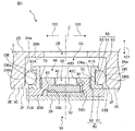
- FIG. 1 is a perspective view of a semiconductor device according to the first embodiment of the present invention.
- FIG. 2 is a cross-sectional view taken along the line AA of FIG.
- the height direction 101, the circumferential direction 102, and the radial direction 103 shown in these figures and the drawings described later are for facilitating the understanding of the present invention and do not limit the invention.
- the base substrate 20 side is defined as the lower side
- the tubular member 60 side is defined as the upper side.
- the circumferential direction 102 is a direction along the circumference of the cylindrical member 60 having a cylindrical shape.
- the radial direction 103 is a direction extending radially from the axis C (see FIG. 2) of the tubular member 60.
- the semiconductor device 10 is a pressure sensor that detects pressure. As shown in FIGS. 1 and 2, the semiconductor device 10 includes a base substrate 20, a circuit element 30 mounted on the base substrate 20, a detection element 40 mounted on the base substrate 20, a resin package 50, and a cylinder. The shape member 60 is provided.
- the base substrate 20 is a rigid substrate such as a glass epoxy substrate or a ceramic substrate, but is not limited to this.
- the base substrate 20 may be a lead frame.
- the base substrate 20 has a rectangular parallelepiped shape thin in the height direction 101. That is, in the first embodiment, the base substrate 20 is a quadrangle in a plan view.
- the shape of the base substrate 20 is not limited to a rectangular parallelepiped shape (a shape that is a quadrangle in a plan view).
- the base substrate 20 may be a polygon other than a quadrangle in a plan view.
- the circuit element 30 is mounted on the upper surface 20A of the base substrate 20.
- the base substrate 20 includes a pad 20B on the upper surface 20A. In FIG. 2, one pad 20B is described, but the number of pads 20B is not limited to one.
- the pad 20B is electrically connected to the circuit element 30 via the bonding wire 82.
- the base substrate 20 includes an external connection terminal (not shown) on the lower surface 20C, which is the back surface of the upper surface 20A.
- the semiconductor device 10 is electrically connected to another external device, for example, a printed circuit board mounted on an electronic device 1 (see FIG. 3) described later by an external connection terminal.
- the circuit element 30 includes an upper surface 30A and a lower surface 30B which is the back surface of the upper surface 30A.
- the circuit element 30 is an element provided with an integrated circuit (ASIC: Application Specific Integrated Circuit) for a specific application.
- ASIC Application Specific Integrated Circuit
- the lower surface 30B of the circuit element 30 is adhered to the upper surface 20A of the base substrate 20 by a die attach film, a die attach material, or the like.
- the circuit element 30 includes a first pad 30C on the upper surface 30A. In FIG. 2, only one first pad 30C is shown, but the number of the first pad 30C is not limited to one.
- the first pad 30C is electrically connected to the pad 20B of the base substrate 20 via the bonding wire 82.
- the circuit element 30 is provided with a second pad 30D on the upper surface 30A separately from the first pad 30C.
- a second pad 30D is described, but the number of the second pad 30D is not limited to one.
- the second pad 30D is electrically connected to the detection element 40 via the bonding wire 81.
- the circuit element 30 includes a signal processing circuit that processes the signal output from the detection element 40 and outputs the processed signal to the base substrate 20.
- the circuit element 30 includes a converter, a filter, a temperature sensor, a processor, a memory, and the like.
- the converter converts the voltage signal output from the detection element 40 into a digital signal.
- the filter filters the digital signal from the converter.
- the temperature sensor detects the temperature.
- the processor corrects the filtered digital signal based on the temperature detected by the temperature sensor.
- the memory stores a correction coefficient or the like used when correcting a digital signal using the detected temperature.
- the detection element 40 is a pressure sensor element for measuring pressure.
- the detection element 40 includes an upper surface 40A and a lower surface 40B which is a back surface of the upper surface 40A.
- the detection element 40 is, for example, a piezo resistance type pressure sensor element or a capacitance type pressure sensor element, and is a MEMS (Micro Electro Mechanical Systems) element.
- the lower surface 40B of the detection element 40 is adhered to the upper surface 30A of the circuit element 30 by a die attach film, a die attach material, or the like. As a result, the detection element 40 is mounted on the upper surface 30A of the circuit element 30.
- the detection element 40 includes a pad 40C on the upper surface 40A. In FIG. 2, one pad 40C is shown, but the number of pads 40C is not limited to one.
- the pad 40C is electrically connected to the second pad 30D of the circuit element 30 via the bonding wire 81. That is, the detection element 40 is electrically connected to the base substrate 20 via the circuit element 30.
- the detection element 40 includes a detection unit 40D on which a pressure acts on the upper surface 40A. That is, the detection unit 40D detects the pressure.
- the detection unit 40D of the detection element 40 which is a pressure sensor element, is a membrane or a diaphragm that receives pressure.
- the detection unit 40D is provided with a passivation film, for example, and is waterproof.
- the resin package 50 is manufactured by molding a hard resin such as a thermosetting resin, for example, an epoxy mold resin, onto the upper surface 20A of the base substrate 20. That is, as shown in FIG. 2, the resin package 50 is provided on the upper surface 20A of the base substrate 20. The portion of the upper surface 20A (particularly the pad 20B) of the base substrate 20 is protected and waterproof by being covered with the resin package 50.
- a hard resin such as a thermosetting resin, for example, an epoxy mold resin
- the circuit element 30, the detection element 40, and the bonding wires 81 and 82 are embedded in the resin package 50.
- the circuit element 30 particularly the first pad 30C and the second pad 30D
- the detection element 40 particularly the pad 40C
- the bonding wires 81 and 82 are protected and waterproof. ..
- the electrical connection between the base substrate 20 and the circuit element 30 and the electrical connection between the circuit element 30 and the detection element 40 are waterproofed by the resin package 50.
- the resin package 50 includes a base 51 and a protruding portion 52.
- the base 51 constitutes the base substrate 20 side of the resin package 50. That is, the base 51 constitutes the lower part of the resin package 50. As shown in FIG. 2, the lower surface 51A of the base 51 is in contact with the upper surface 20A of the base substrate 20. That is, the base 51 is provided on the upper surface 20A of the base substrate 20.
- the base 51 has a rectangular parallelepiped shape thin in the height direction 101. That is, in the first embodiment, the base 51 is a quadrangle in a plan view. In a plan view, the base 51 and the base substrate 20 have the same shape and the same size. As a result, the outer surface 51Ca of the base 51 and the outer surface 20Da of the base substrate 20 are flush with each other.
- the shape of the base 51 is not limited to a rectangular parallelepiped shape (a shape that is a quadrangle in a plan view).
- the base 51 may be a polygon other than a quadrangle in a plan view.
- the base 51 may be circular, for example, other than a polygon in a plan view.
- the base 51 and the base substrate 20 may have different shapes or different sizes.
- the protruding portion 52 constitutes the opposite side of the base substrate 20 with respect to the base portion 51 of the resin package 50. That is, the protruding portion 52 constitutes the upper portion of the resin package 50.
- the protruding portion 52 protrudes from the base portion 51 so as to be separated from the base substrate 20. In other words, the protruding portion 52 protrudes upward from the base 51.
- the protruding portion 52 is inserted into the tubular member 60, which will be described later.
- the protrusion 52 is provided at the center of the base 51 in a plan view.
- the base 51 extends outward from the outer surface 52A of the protrusion 52.
- the circuit element 30, the lower part of the detection element 40, the lower part of the bonding wire 81, and the bonding wire 82 are embedded in the base 51.
- the upper portion of the detection element 40 and the upper portion of the bonding wire 81 are embedded in the protrusion 52.
- the lower portion of the circuit element 30 may be embedded in the base portion 51, and the upper portion of the circuit element 30 may be embedded in the protruding portion 52. Further, the lower portion of the bonding wire 82 may be embedded in the base portion 51, and the upper portion of the bonding wire 82 may be embedded in the protruding portion 52. Further, the entire detection element 40 may be embedded in the base 51. Further, the entire bonding wire 81 may be embedded in the base 51.
- the protruding portion 52 includes an exposed hole 53.
- the exposed hole 53 penetrates the protruding portion 52 in the vertical direction. That is, the protruding portion 52 has a cylindrical shape.
- the outer shape of the protruding portion 52 is matched to the shape of the inner peripheral surface 61B of the main body portion 61 of the tubular member 60, which will be described later.
- the inner peripheral surface 61B of the main body 61 of the tubular member 60 has a circular shape in a plan view. Therefore, the outer shape of the protruding portion 52 is also circular in a plan view. That is, in the first embodiment, the protruding portion 52 has a cylindrical shape.
- the outer shape of the protruding portion 52 also has another shape. For example, when the inner peripheral surface 61B of the tubular member 60 is a quadrangle in a plan view, the outer shape of the protruding portion 52 is a square cylinder.
- the opening of the exposed hole 53 is provided on the upper surface 52B of the protruding portion 52. That is, the resin package 50 exposes the detection unit 40D of the detection element 40 upward.
- a pressure acts on the detection unit 40D of the detection element 40 from the outside of the semiconductor device 10 via the cylindrical member 60 and the exposed hole 53, which will be described later, and the detection element 40 can measure the pressure.
- the protrusion 52 is located around the detection unit 40D of the detection element 40 in a plan view. That is, the protruding portion 52 is located outside the detection portion 40D in a plan view.
- the detection unit 40D which is a portion exposed to the outside by the exposure hole 53, is waterproofed by, for example, a passivation film.
- the shape of the exposed hole 53 is a square shape in a plan view, but may be another shape (for example, a circular shape in a plan view).
- the exposed hole 53 may function as a pressure introduction hole for introducing pressure into the detection unit 40D.
- the tubular member 60 is made of a metal such as stainless steel.
- the tubular member may be made of a material other than metal.
- the tubular member may be made of resin. Examples of the resin include a hard resin constituting the resin package 50.
- the tubular member 60 includes a main body portion 61, an upper flange portion 62, and a lower flange portion 63.
- the lower flange portion 63 is an example of the flange portion.
- the main body portion 61, the upper flange portion 62, and the lower flange portion 63 may be integrally molded, or may be composed of separate members and may be combined by fitting or the like.
- the main body 61 has a cylindrical shape in the first embodiment.
- the protruding portion 52 of the resin package 50 enters the internal space 64 of the main body portion 61 from below.
- the outer shape of the protruding portion 52 is matched to the shape of the inner peripheral surface 61B of the main body portion 61 of the tubular member 60. Therefore, the outer surface 52A of the protrusion 52 faces the inner peripheral surface 61B of the main body 61.
- a slight gap is formed between the outer surface 52A of the protrusion 52 and the inner peripheral surface 61B of the main body 61.
- the adhesive 70 is interposed in this gap.
- the outer surface 52A of the protruding portion 52 is adhered to the inner peripheral surface 61B of the main body portion 61.
- the outer surface 52A of the protrusion 52 may be in contact with the inner peripheral surface 61B of the main body 61.
- the upper flange portion 62 projects in the radial direction 103 from the outer surface 61A of the main body portion 61.
- the upper flange portion 62 is located at the upper end portion of the main body portion 61.
- the upper flange portion 62 projects over the entire circumference of the outer surface 61A in the circumferential direction 102.
- the upper flange portion 62 is circular in a plan view.
- the upper flange portion 62 may be located at a position other than the upper end portion of the main body portion 61. Further, the upper flange portion 62 may project from a part of the outer surface 61A in the circumferential direction 102.
- the tubular member 60 may include a plurality of upper flange portions 62 arranged at intervals in the circumferential direction 102. Further, the upper flange portion 62 may have a shape other than a circle in a plan view, for example, a quadrangle in a plan view.
- the lower flange portion 63 projects in the radial direction 103 from the outer surface 61A of the main body portion 61.
- the lower flange portion 63 is located below the upper flange portion 62, and is located at a distance from the upper flange portion 62 in the height direction 4.
- the lower flange portion 63 is located at the lower end portion of the main body portion 61.
- the lower flange portion 63 projects over the entire circumference of the outer surface 61A in the circumferential direction 102.
- the lower flange portion 63 is circular in a plan view.
- the lower surface 60A of the lower flange portion 63 is in contact with the upper surface 51B of the base portion 51 of the resin package 50 from above. That is, the lower flange portion 63 is supported by the base portion 51 of the resin package 50.
- the lower flange portion 63 is located inside the outer edge portion 51C of the base portion 51 of the resin package 50 in a plan view.
- the outer edge portion 51C of the base portion 51 is a portion formed by the outer surface 51Ca of the base portion 51 and the vicinity of the outer surface 51Ca of the base portion 51.
- the lower flange portion 63 may be located at a position other than the lower end portion of the main body portion 61.
- the lower end of the main body 61 is located below the lower flange 63, and the lower end of the main body 61 is supported by the base 51 of the resin package 50.
- the lower flange portion 63 may project from a part of the outer surface 61A in the circumferential direction 102.
- the tubular member 60 may include a plurality of lower flange portions 63 arranged at intervals in the circumferential direction 102.
- the lower flange portion 63 may have a shape other than a circle in a plan view, for example, a quadrangle in a plan view.
- the upper surface 52B of the protruding portion 52 is located above the lower flange portion 63 in a state where the protruding portion 52 of the resin package 50 has entered the main body portion 61 from below. That is, the protruding portion 52 protrudes above the lower flange portion 63.
- the position of the upper surface 52B of the protrusion 52 is not limited to the position shown in FIG.
- the upper surface 52B of the protruding portion 52 may be located below the upper end of the lower flange portion 63.
- the upper surface 52B of the protruding portion 52 may be at the same height as the upper end portion of the tubular member 60.
- FIG. 3 is a diagram corresponding to a cross section along the line AA of FIG. 1 in a state where the semiconductor device of FIG. 1 is attached to an electronic device.
- FIG. 4 is a diagram corresponding to a cross section along the line BB of FIG. 1 in a state where the semiconductor device of FIG. 1 is attached to an electronic device.
- the semiconductor device 10 is used by being attached to the housing 2 of the electronic device 1.
- the electronic device 1 is, for example, a pressure measuring device, and includes a semiconductor device 10, an O-ring OR, and a housing 2.
- the O-ring OR is fitted to the tubular member 60 of the semiconductor device 10.
- the O-ring OR is annular.
- the inner diameter of the O-ring OR is the same as or substantially the same as the outer diameter of the main body 61 of the tubular member 60.
- the O-ring OR is made of a member that is easily compressed and deformed, such as nitrile rubber.
- the O-ring OR is arranged so as to surround the main body 61 of the tubular member 60 in a plan view.
- the inner diameter of the O-ring OR is larger than the outer diameter of the main body 61.
- the O-ring OR attached to the main body portion 61 of the tubular member 60 is restricted from coming off from the upper end portion of the main body portion 61 by the upper flange portion 62 of the tubular member 60.
- the O-ring OR mounted on the main body 61 is restricted from coming off from the lower end of the main body 61 by the lower flange portion 63 of the tubular member 60.
- the upper flange portion 62 of the tubular member 60 may be omitted. In that case, the inner diameter of the O-ring OR is smaller than the outer diameter of the main body 61 so that the O-ring OR does not loosely fit.
- the housing 2 has a recess 2A and an opening 2B.
- the recess 2A is recessed from the inner surface 2C of the housing 2 toward the outer surface 2D of the housing 2.
- the inner surface 2C of the housing 2 faces the internal space of the housing 2.
- the outer surface 2D of the housing 2 is the back surface of the inner surface 2C and faces the outside of the housing 2.
- the semiconductor device 10 equipped with the O-ring OR is arranged in the recess 2A.
- the O-ring OR, the tubular member 60, the protruding portion 52 of the resin package 50, and the upper portion of the detection element 40 are arranged in the recess 2A.
- the semiconductor device 10 arranged in the recess 2A is attached to the housing 2 by a known means (not shown) such as fitting. Further, the portion of the semiconductor device 10 that is arranged in the recess 2A is not limited to the above-mentioned portion. Of the semiconductor device 10, at least the O-ring OR and the tubular member 60 may be arranged in the recess 2A.
- the opening 2B penetrates the housing 2.
- the opening 2B communicates the outside of the housing 2 with the recess 2A. That is, the opening 2B opens the recess 2A to the outside of the housing 2.
- the detection unit 40D of the detection element 40 of the semiconductor device 10 has an exposed hole 53 of the resin package 50, an internal space 64 of the main body 61 of the tubular member 60, a recess 2A of the housing 2, and an opening 2B of the housing 2. It communicates with the outside of the electronic device 1 via the device 1. That is, the opening 2B exposes the detection unit 40D to the outside of the housing 2 via the tubular member 60. Thereby, the external pressure of the electronic device 1 can be measured by the semiconductor device 10.
- the O-ring OR is arranged in the gap between the semiconductor device 10 arranged as described above and the inner side surface 2Aa constituting the recess 2A of the housing 2.
- the length 103 in the radial direction between the outer surface 61A of the main body 61 of the tubular member 60 and the inner surface 2Aa constituting the recess 2A is , Shorter than the diameter R of the O-ring OR (see FIG. 2). Therefore, when the semiconductor device 10 is arranged in the recess 2A, the O-ring OR is compressed and deformed (see FIGS. 3 and 4).
- the inner peripheral portion ORa of the O-ring OR contacts the outer surface 61A of the main body portion 61 of the tubular member 60, and the outer peripheral portion ORb of the O-ring OR contacts the inner side surface 2Aa constituting the recess 2A.
- the gap between the semiconductor device 10 and the housing 2 is sealed, and the O-ring OR prevents the liquid from entering the inside of the electronic device 1 from the outside of the electronic device 1 through the gap.
- the inner side surface 2Aa constituting the concave portion 2A of the housing 2 has a tapered surface 2F at the end 2E on the inner surface 2C side of the housing 2.
- the end portion 2E on the inner surface 2C side of the housing 2 is a portion formed by the inner surface 2C of the housing 2 and the vicinity of the inner surface 2C of the housing 2.
- the tapered surface 2F is a surface inclined with respect to the height direction 4.
- the tapered surface 2F is directed toward the axis C of the tubular member 60 from the inner surface 2C toward the outer surface 2D.
- the tapered surface 2F is inclined with respect to the height direction 4 so that the inner diameter of the recess 2A becomes smaller from the inner surface 2C toward the outer surface 2D.
- the presence or absence of the tapered surface 2F is arbitrary.
- the semiconductor device 10 is inserted into the recess 2A from the internal space side of the housing 2 with the upper flange portion 62 side of the tubular member 60 as the head.
- the O-ring OR comes into contact with the tapered surface 2F from the internal space side of the housing 2.
- the O-ring OR When the semiconductor device 10 is further inserted into the recess 2A, the O-ring OR is guided along the tapered surface 2F. At this time, a reaction force acts from the tapered surface 2F to the O-ring OR. This reaction force includes a component in the direction toward the axis C. This component compresses the O-ring OR. The compressed O-ring OR passes through the tapered surface 2F. As a result, as described above, the inner peripheral portion ORa of the O-ring OR is in contact with the outer surface 61A of the main body portion 61 of the tubular member 60, and the outer peripheral portion ORb of the O-ring OR is the inner surface surface constituting the recess 2A. Contact 2Aa. As a result, the gap between the semiconductor device 10 and the housing 2 is sealed.
- the upper surface 51B of the base 51 of the resin package 50 comes into contact with the inner surface 2C of the housing 2.
- the peripheral portion of the apex of the quadrangle comes into contact with the inner surface 2C of the housing 2.
- the semiconductor device 10 is positioned with respect to the housing 2. That is, it is restricted that the semiconductor device 10 is inserted into the recess 2A more than necessary.
- the lower flange portion 63 is located inside the outer edge portion 51C of the base portion 51 in a plan view. Therefore, when the semiconductor device 10 in which the O-ring OR is fitted in the main body 61 of the tubular member 60 is arranged in the recess 2A of the housing 2 of the electronic device 1, the lower flange 63 is also arranged in the recess 2A. In this case, the diameter of the recess 2A can be reduced by the amount that the lower flange portion 63 is located inside the outer edge portion 51C of the base portion 51. As a result, the gap between the lower flange portion 63 and the inner side surface 2Aa of the housing 2 constituting the recess 2A can be reduced.
- the lower flange portion 63 is located inside the outer edge portion 51C of the base portion 51 in a plan view, but a part of the lower flange portion 63 is located outside the outer edge portion 51C of the base portion 51. May be.
- a part of the lower flange portion 63 may be located outside the central portion of the four sides of the upper surface 51B of the base portion 51. That is, if the peripheral portion of the apex of the upper surface 51B of the base portion 51 is located outside the lower flange portion 63, the peripheral portion comes into contact with the inner surface 2C of the housing 2, so that the semiconductor device 10 is the housing. Positioned relative to 2.
- the outer surface 52A of the protrusion 52 is adhered to the inner peripheral surface 61B of the tubular member 60. Even if the adhesive 70 between the outer surface 52A of the protruding portion 52 and the inner peripheral surface 61B of the tubular member 60 protrudes, the protruding adhesive 70 is the internal space 64 of the tubular member 60 or the tubular shape. It is located below the lower flange portion 63 of the member 60. Therefore, the protruding adhesive 70 does not hinder the attachment of the semiconductor device 10 to the housing 2.
- the lower flange portion 63 of the tubular member 60 and the base portion 51 of the resin package 50 do not necessarily have to be adhered to each other, it is not necessary to increase the contact area between the lower flange portion 63 and the base portion 51. Further, it is not necessary to perform complicated processing such as providing a recess for attracting the adhesive of the lower flange portion 63.
- the lower flange portion 63 is circular like the O-ring OR fitted to the main body portion 61 of the tubular member 60. Therefore, the gap between the lower flange portion 63 and the inner side surface 2Aa of the housing 2 constituting the recess 2A can be reduced, and the variation in the gap can be eliminated.
- the main body portion 61 has a cylindrical shape. As a result, when the O-ring OR is fitted to the main body 61, a gap is unlikely to occur between the O-ring OR and the main body 61. As a result, it is possible to reduce the possibility that the liquid will flow between the O-ring OR and the main body 61.
- the lower flange portion 63 projects from the outer surface 61A of the main body portion 61 to the entire circumference of the main body portion 61. Therefore, the O-ring OR can be stably supported by the lower flange portion 63 in a state where the O-ring OR is fitted to the main body portion 61.
- the protruding portion 52 protrudes above the lower flange portion 63 of the tubular member 60. Therefore, in a state where the O-ring OR is fitted to the main body 61 of the tubular member 60, the semiconductor so that the protruding portion 52 faces the O-ring OR in the radial direction 103 with the main body 61 of the tubular member 60 interposed therebetween.
- the device 10 can be configured.
- the protrusion 52 can receive the deformation of the main body 61 of the tubular member 60 due to the force acting on the main body 61 of the tubular member 60 from the O-ring OR, so that the deformation can be suppressed.
- the tubular member 60 is made of metal, the dimensional accuracy of the tubular member 60 can be improved.
- the adhesive strength when the tubular member 60 is adhered to the resin package 50 which is also made of resin can be increased.
- the tapered surface 2F is O.
- the main body 61 of the tubular member 60 may be cylindrical and is not limited to a cylindrical shape.
- the main body portion 61 may have an elliptical cylinder shape or a polygonal cylinder shape.
- the detection element 40 is mounted on the upper surface 30A of the circuit element 30, but the detection element 40 may be mounted on the upper surface 20A of the base substrate 20 by adhesion or the like.
- the circuit element 30 is electrically connected to the base substrate 20 via the bonding wire 82, and the detection element 40 is electrically connected to the circuit element 30 via the bonding wire 81.
- the connection mode of the base substrate 20, the circuit element 30, and the detection element 40 is not limited to this.
- the detection element 40 may be connected to the base substrate 20 via a bonding wire in the same manner as the circuit element 30. In this case, the detection element 40 is electrically connected to the circuit element 30 via the base substrate 20.
- the base substrate 20, the circuit element 30, and the detection element 40 are electrically connected via the bonding wires 81 and 82, respectively.
- the base substrate 20, the circuit element 30, and the detection element 40 may be electrically connected by means other than the bonding wires 81 and 82.
- the circuit element 30 may be mounted on the base substrate 20 by a flip chip. In this case, the circuit element 30 and the base substrate 20 are electrically connected by solder.
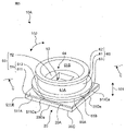
- FIG. 5 is a perspective view of the semiconductor device according to the second embodiment of the present invention.
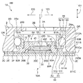
- FIG. 6 is a diagram corresponding to a cross section along the line CC of FIG. 5 in a state where the semiconductor device of FIG. 5 is attached to an electronic device.
- the semiconductor device 10A according to the second embodiment is different from the semiconductor device 10 according to the first embodiment in that the base portion 51 of the resin package 50 includes a first base portion 511 and a second base portion 512.
- the base 51 of the resin package 50 includes a first base 511 and a second base 512.
- the first base portion 511 constitutes the base substrate 20 side of the base 51. That is, the first base portion 511 constitutes the lower portion of the base portion 51.
- the lower surface 511A of the first base portion 511 is in contact with the upper surface 20A of the base substrate 20. That is, the first base portion 511 is provided on the upper surface 20A of the base substrate 20.
- the first base portion 511 has a rectangular parallelepiped shape thin in the height direction 101. That is, in the second embodiment, the first base portion 511 is a quadrangle in a plan view. In a plan view, the first base portion 511 and the base substrate 20 have the same shape and the same size. As a result, the outer surface 511Ca of the first base portion 511 and the outer surface 20Da of the base substrate 20 are flush with each other.
- the shape of the first base portion 511 is not limited to a rectangular parallelepiped shape (a shape that is a quadrangle in a plan view).
- the first base portion 511 may be a polygon other than a quadrangle in a plan view.
- the first base portion 511 may be circular, for example, other than a polygon in a plan view.
- the first base portion 511 and the base substrate 20 may have different shapes or different sizes.
- the second base portion 512 constitutes the opposite side of the base substrate 20 with respect to the first base portion 511 of the base 51. That is, the second base portion 512 constitutes the upper portion of the base portion 51.
- the second base portion 512 protrudes from the first base portion 511 so as to be separated from the base substrate 20. In other words, the second base 512 projects upward from the first base 511.
- the second base portion 512 has a cylindrical shape. That is, the second base portion 512 is circular in a plan view.
- the second base portion 512 may have a shape other than a cylinder, for example, a quadrangular prism shape. In this case, the second base 512 is a quadrangle in a plan view.
- the upper surface 512A of the second base portion 512 is in contact with the lower surface 60A of the lower flange portion 63 of the tubular member 60 from below. That is, the second base portion 512 supports the lower flange portion 63 of the tubular member 60.
- the second base portion 512 is located inside the outer edge portion 511C of the first base portion 511 in a plan view.
- the outer edge portion 511C of the first base portion 511 is a portion formed by the vicinity of the outer surface 511Ca of the first base portion 511 and the outer surface 511Ca of the first base portion 511.
- the protruding portion 52 protrudes upward from the second base portion 512.
- the semiconductor device 10A according to the second embodiment is inserted into the recess 2A of the housing 2 in the same manner as the semiconductor device 10 according to the first embodiment.
- the electronic device 1A includes a semiconductor device 10A, an O-ring OR mounted on the semiconductor device 10A, and a housing 2.
- the upper surface 511B of the first base portion 511 is in contact with the inner surface 2C of the housing 2.
- the peripheral portion of the apex of the quadrangle is in contact with the inner surface 2C of the housing 2.
- the central portion in other words, adjacent to each other
- the central portion of the quadrangular upper surface 511B of the first base portion 511.
- the middle portion of the two vertices is not in contact with the inner surface 2C of the housing 2.
- the O-ring OR, the tubular member 60, the protruding portion 52 of the resin package 50, the second base portion 512, the upper portion of the detection element 40, and the upper portion of the circuit element 30 are arranged in the recess 2A. Has been done.
- the second base portion 512 is located inside the outer edge portion 511C of the first base portion 511 in a plan view. Therefore, when the semiconductor device 10A in which the O-ring OR is fitted in the main body portion 61 of the tubular member 60 is arranged in the recess 2A of the housing 2 of the electronic device 1A, not only the tubular member 60 but also the second base portion. When the 512 is also arranged in the recess 2A, the diameter of the recess 2A can be reduced by the amount that the second base 512 is located inside the outer edge portion 511C of the first base 511.
- the gap between the lower flange portion 63 and the inner side surface 2Aa of the housing 2 constituting the recess 2A can be reduced. Further, by inserting the second base portion 512 into the recess 2A, the O-ring OR fitted in the main body portion 61 of the tubular member 60 can be inserted deeper into the recess 2A.
- the second base portion 512 is circular like the O-ring OR fitted to the main body portion 61 of the tubular member 60. Therefore, the gap between the second base portion 512 and the inner side surface 2Aa of the housing 2 constituting the recess 2A can be reduced, and the variation in the gap can be eliminated.
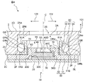
- FIG. 7 is a perspective view of the semiconductor device according to the third embodiment of the present invention.
- FIG. 8 is a diagram corresponding to a cross section along the DD line of FIG. 7 in a state where the semiconductor device of FIG. 7 is attached to an electronic device.
- the difference between the semiconductor device 10B according to the third embodiment and the semiconductor device 10 according to the first embodiment is that the resin package 50A is located inside the outer edge portion of the base substrate 20 in a plan view.
- the semiconductor device 10B includes a resin package 50A.
- the resin package 50A includes a base portion 54 having a configuration different from that of the base portion 51 of the first embodiment, and a protruding portion 52 having the same configuration as that of the first embodiment and protruding upward from the base portion 54.
- the base portion 54 is located inside the outer edge portion 20D (see FIG. 8) of the base substrate 20 in a plan view.
- the outer edge portion 20D of the base substrate 20 is a portion formed by the outer surface 20Da of the base substrate 20 and the vicinity of the outer surface 20Da of the base substrate 20.
- the base 51 (see FIG. 1), which has the same size as the base substrate 20 in a plan view, and the base 54 have different configurations.
- the outer edge portion 54C of the base portion 54 is located inside the outer edge portion 20D of the base substrate 20.
- the outer edge portion 54C of the base portion 54 is a portion composed of the outer surface 54Ca of the base portion 54 and the vicinity of the outer surface 54Ca of the base portion 54.
- the protruding portion 52 is located inside the outer edge portion 54C of the base portion 54.
- the resin package 50A including the base portion 54 and the protruding portion 52 is located inside the outer edge portion 20D of the base substrate 20 in a plan view.
- the base 54 has a cylindrical shape. That is, the base 54 is circular in a plan view. That is, the resin package 50 including the base 54 is circular in a plan view.
- the base 54 may have a shape other than a cylinder.
- the base 54 may have a quadrangular prism shape. In this case, the resin package 50 including the base 54 is a quadrangle in a plan view.
- the base substrate 20 has a thin rectangular parallelepiped shape in the height direction 101 as in the first embodiment. That is, the base substrate 20 is a quadrangle in a plan view.
- the shape of the base substrate 20 is not limited to a rectangular parallelepiped shape (a shape that is a quadrangle in a plan view).
- the base substrate 20 may be a polygon other than a quadrangle in a plan view.
- the upper surface 54B of the base portion 54 is in contact with the lower surface 60A of the lower flange portion 63 of the tubular member 60 from below. That is, the base portion 54 supports the lower flange portion 63 of the tubular member 60.
- the semiconductor device 10B according to the third embodiment is inserted into the recess 2A of the housing 2 in the same manner as the semiconductor device 10 according to the first embodiment.
- the electronic device 1B includes a semiconductor device 10B, an O-ring OR mounted on the semiconductor device 10B, and a housing 2.
- the upper surface 20A of the base substrate 20 is in contact with the inner surface 2C of the housing 2.
- the peripheral portion of the apex of the quadrangle is in contact with the inner surface 2C of the housing 2.
- the semiconductor device 10B is positioned with respect to the housing 2.
- the central portion of the side of the quadrangle (in other words, adjacent 2).
- the middle portion of the two vertices) is not in contact with the inner surface 2C of the housing 2.
- all parts of the semiconductor device 10B except the base substrate 20 are arranged in the recess 2A.
- the resin package 50A is located inside the outer edge portion 20D of the base substrate 20 in a plan view. Therefore, when the semiconductor device 10B in which the O-ring OR is fitted in the main body 61 of the tubular member 60 is arranged in the recess 2A of the housing 2 of the electronic device 1B, the entire resin package 50A is arranged in the recess 2A. In this case, the diameter of the recess 2A can be reduced by the amount that the resin package 50A is located inside the outer edge portion 20D of the base substrate 20. As a result, the gap between the lower flange portion 6 and the inner side surface 2Aa of the housing 2 constituting the recess 2A can be reduced. Further, by inserting the entire resin package 50A into the recess 2A, the O-ring OR fitted in the main body 61 of the tubular member 60 can be inserted deeper into the recess 2A.
- the resin package 50A in a plan view, is circular like the O-ring OR fitted to the tubular member 60. Therefore, the gap between the resin package 50A and the inner side surface 2Aa of the housing 2 constituting the recess 2A can be reduced, and the variation in the gap can be eliminated.
Landscapes
- Physics & Mathematics (AREA)
- General Physics & Mathematics (AREA)
- Chemical & Material Sciences (AREA)
- Analytical Chemistry (AREA)
- Measuring Fluid Pressure (AREA)
Abstract
接着剤のはみ出し規制のための複雑な加工が不要であり、且つ筐体内部への液体の浸入を防止可能な態様で筐体に取付可能な半導体装置を提供する。本発明に係る半導体装置10は、ベース基板20上に実装され、圧力を検出する検出部40Dを備える検出素子40と、ベース基板20上に設けられた樹脂パッケージ50と、樹脂パッケージ50に支持された筒状部材60とを備える。樹脂パッケージ50は、ベース基板20上に設けられ、検出素子40が埋設された基部51と、検出部40Dを露出させる露出穴53を有し、基部51から筒状部材60内へ突出した突出部52とを備える。筒状部材60は、筒状の本体部61と、基部51に支持された下フランジ部63とを備える。下フランジ部63は、平面視において基部51の外縁部51Cより内側に位置する。突出部52の外側面52Aは、筒状部材60の内周面61Bと接着されている。
Description
本発明は、圧力を測定する半導体装置、及び当該半導体装置を備えた電子機器に関する。
特許文献1には、圧力を測定する圧力センサが開示されている。圧力センサは、圧力測定装置等の筐体に取り付けられる。圧力センサは、基板と、基材に設けられた枠部に接着された筒状のキャップとを備えている。キャップの周りには、円環状のOリングが嵌装されている。圧力センサが筐体に取り付けられた状態において、筐体と圧力センサとの間の隙間が、Oリングによって封止される。これにより、隙間を介して筐体の外部から筐体の内部に液体が浸入することが防止されている。
しかしながら、特許文献1に開示された圧力センサでは、キャップにおける枠部との接着面が小さい。接着面が小さい場合、キャップを枠部に接着するときに接着剤がキャップからはみ出すおそれがある。そのため、圧力センサでは、接着剤のはみ出しを防止するために、接着剤を誘引するための凹部を接着面に設ける複雑な加工が施されている。
これに対して、特許文献2に開示された圧力を測定する半導体装置では、上記のキャップに対応する筒状部材が外方へ張り出したフランジ部を備えており、フランジ部が樹脂パッケージと接着される。フランジ部は外方へ張り出しているため、フランジ部における樹脂パッケージとの接着面は、特許文献1に開示された圧力センサのキャップの接着面より大きい。そのため、当該半導体装置では、特許文献1に開示された圧力センサのキャップのような複雑な加工を行うことなく、接着剤のはみ出しを少なくすることができる。
しかしながら、特許文献2に開示された半導体装置では、筒状部材がフランジ部を備えていることによって、以下に説明する問題が発生する。半導体装置は、Oリングが筒状部材に嵌装された状態で、筐体に設けられた取り付け穴に挿入されることによって、筐体に取り付けられる。このとき、取り付け穴の開口部の屈曲した縁部にOリングが引っ掛かり、半導体装置及びOリングの筐体への取り付けが困難になるおそれがある。
これを解決するために、取り付け穴の開口部の縁部に面取りを施すことが考えられる。しかし、面取りが施された場合、Oリングが嵌装された半導体装置が筐体に取り付けられた状態において、Oリングと筐体の面取り部分との間に隙間が生じるおそれがある。この場合、筐体の内部への液体の浸入を十分に防止できないおそれがある。
これを解決するために、Oリングに加えて、Oリングより手前側に位置するフランジ部も、取り付け穴に挿入されるように、取り付け穴の外径を大きくすることが考えられる。これにより、手前側のフランジ部も取り付け穴に挿入される分、Oリングを筐体の面取り部分より奥まで挿入することができる。そのため、Oリングと筐体の面取り部分との隙間が大きくなるという問題は生じない。
しかしながら、特許文献2に開示された半導体装置では、平面視において、Oリングが円形であるために取り付け穴が円形に形成されているのに対して、フランジ部は矩形である。つまり、フランジ部が挿入可能となるように取り付け穴の直径を大きくする必要がある。この場合、フランジ部の矩形の各辺の中央部において、取り付け穴を構成する筐体の内側面とフランジ部との隙間が大きくなってしまう。すると、当該中央部において、Oリングは十分に支持されないため、Oリングが垂れ下がってしまうおそれがある。この場合、筐体の内部への液体の浸入を十分に防止できないおそれがある。
特許文献1に開示された圧力センサは、フランジ部を備えていないために、上記の問題は生じないが、上述したように接着剤のはみ出し規制のための複雑な加工が必要となってしまう。
従って、本発明の目的は、前記課題を解決することにあって、接着剤のはみ出し規制のための複雑な加工が不要であり、且つ筐体内部への液体の浸入を防止可能な態様で筐体に取り付け可能な半導体装置を提供することにある。
前記目的を達成するために、本発明は以下のように構成する。
本発明の一態様に係る半導体装置は、
ベース基板と、
前記ベース基板の上面に実装され、圧力を検出する検出部を備える検出素子と、
前記ベース基板の上面に設けられ、前記検出素子が埋設され、前記検出素子の前記検出部を上方へ露出させる露出穴を有する樹脂パッケージと、
前記樹脂パッケージに支持された筒状部材と、を備え、
前記樹脂パッケージは、
前記ベース基板の上面に設けられ、前記検出素子が埋設された基部と、
前記露出穴を有し、前記基部から上方へ突出して前記筒状部材に入り込んだ突出部と、を備え、
前記筒状部材は、
円筒状の本体部と、
前記本体部の外側面から前記本体部の全周に亘って張り出し、前記基部に支持されたフランジ部と、を備え、
前記フランジ部の少なくとも一部は、平面視において前記樹脂パッケージの前記基部の外縁部より内側に位置し、
前記突出部の外側面は、前記筒状部材の内周面と接着されている。
本発明の一態様に係る半導体装置は、
ベース基板と、
前記ベース基板の上面に実装され、圧力を検出する検出部を備える検出素子と、
前記ベース基板の上面に設けられ、前記検出素子が埋設され、前記検出素子の前記検出部を上方へ露出させる露出穴を有する樹脂パッケージと、
前記樹脂パッケージに支持された筒状部材と、を備え、
前記樹脂パッケージは、
前記ベース基板の上面に設けられ、前記検出素子が埋設された基部と、
前記露出穴を有し、前記基部から上方へ突出して前記筒状部材に入り込んだ突出部と、を備え、
前記筒状部材は、
円筒状の本体部と、
前記本体部の外側面から前記本体部の全周に亘って張り出し、前記基部に支持されたフランジ部と、を備え、
前記フランジ部の少なくとも一部は、平面視において前記樹脂パッケージの前記基部の外縁部より内側に位置し、
前記突出部の外側面は、前記筒状部材の内周面と接着されている。
本発明によれば、接着剤のはみ出し規制のための複雑な加工が不要であり、且つ筐体内部への液体の浸入を防止可能な態様で筐体に取り付け可能である。
本発明の一態様に係る半導体装置は、
ベース基板と、
前記ベース基板の上面に実装され、圧力を検出する検出部を備える検出素子と、
前記ベース基板の上面に設けられ、前記検出素子が埋設され、前記検出素子の前記検出部を上方へ露出させる露出穴を有する樹脂パッケージと、
前記樹脂パッケージに支持された筒状部材と、を備え、
前記樹脂パッケージは、
前記ベース基板の上面に設けられ、前記検出素子が埋設された基部と、
前記露出穴を有し、前記基部から上方へ突出して前記筒状部材に入り込んだ突出部と、を備え、
前記筒状部材は、
筒状の本体部と、
前記本体部の外側面から張り出し、前記基部に支持されたフランジ部と、を備え、
前記フランジ部の少なくとも一部は、平面視において前記樹脂パッケージの前記基部の外縁部より内側に位置し、
前記突出部の外側面は、前記筒状部材の内周面と接着されている。
ベース基板と、
前記ベース基板の上面に実装され、圧力を検出する検出部を備える検出素子と、
前記ベース基板の上面に設けられ、前記検出素子が埋設され、前記検出素子の前記検出部を上方へ露出させる露出穴を有する樹脂パッケージと、
前記樹脂パッケージに支持された筒状部材と、を備え、
前記樹脂パッケージは、
前記ベース基板の上面に設けられ、前記検出素子が埋設された基部と、
前記露出穴を有し、前記基部から上方へ突出して前記筒状部材に入り込んだ突出部と、を備え、
前記筒状部材は、
筒状の本体部と、
前記本体部の外側面から張り出し、前記基部に支持されたフランジ部と、を備え、
前記フランジ部の少なくとも一部は、平面視において前記樹脂パッケージの前記基部の外縁部より内側に位置し、
前記突出部の外側面は、前記筒状部材の内周面と接着されている。
この構成によれば、フランジ部の少なくとも一部は、平面視において基部の外縁部より内側に位置している。そのため、筒状部材の本体部にOリングが嵌装された半導体装置が電子機器の筐体の凹部に配置されるときに、フランジ部も凹部に配置された場合、フランジ部の少なくとも一部が基部の外縁部より内側に位置している分だけ、凹部の直径を小さくすることができる。これにより、フランジ部と凹部を構成する筐体の内側面との隙間を小さくすることができる。
この構成によれば、突出部の外側面が筒状部材の内周面と接着されている。仮に、突出部の外側面と筒状部材の内周面との間の接着剤がはみ出したとしても、はみ出した接着剤は、筒状部材の内部に位置している。そのため、はみ出した接着剤が、半導体装置の筐体への取り付けを阻害することはない。
また、筒状部材のフランジ部と樹脂パッケージの基部とは必ずしも接着する必要がないため、フランジ部と基部との接触面積を大きくする必要はない。また、フランジ部に接着剤を誘引するための凹部を設ける等の複雑な加工を施す必要はない。
前記樹脂パッケージの前記基部は、平面視において多角形であり、前記筒状部材の前記フランジ部は、平面視において円形であってもよい。この構成によれば、平面視において、フランジ部は、筒状部材の本体部に嵌装されるOリングと同様に円形である。そのため、フランジ部と凹部を構成する筐体の内側面との隙間を小さくできると共に、当該隙間のばらつきを無くすことができる。
前記樹脂パッケージの前記基部は、前記ベース基板の上面に設けられた第1基部と、前記第1基部から上方へ突出し、平面視において前記第1基部の外縁部より内側に位置し、前記筒状部材の前記フランジ部を支持する第2基部と、を備えていてもよい。
この構成によれば、第2基部は、平面視において第1基部の外縁部より内側に位置している。そのため、筒状部材の本体部にOリングが嵌装された半導体装置が電子機器の筐体の凹部に配置されるときに、筒状部材だけでなく第2基部も凹部に配置された場合、第2基部が第1基部の外縁部より内側に位置している分だけ凹部の直径を小さくすることができる。これにより、フランジ部と凹部を構成する筐体の内側面との隙間を小さくすることができる。また、第2基部が凹部に挿入されることによって、筒状部材の本体部に嵌装されたOリングを凹部のより奥まで挿入することができる。
前記樹脂パッケージの前記第1基部は、平面視において多角形であり、前記樹脂パッケージの前記第2基部は、平面視において円形であってもよい。この構成によれば、平面視において、第2基部は、筒状部材の本体部に嵌装されるOリングと同様に円形である。そのため、第2基部と凹部を構成する筐体の内側面との隙間を小さくできると共に、当該隙間のばらつきを無くすことができる。
前記樹脂パッケージは、平面視において前記ベース基板の外縁部より内側に位置していてもよい。この構成によれば、樹脂パッケージは、平面視においてベース基板の外縁部より内側に位置している。そのため、筒状部材の本体部にOリングが嵌装された半導体装置が電子機器の筐体の凹部に配置されるときに、樹脂パッケージ全体が凹部に配置された場合、樹脂パッケージがベース基板の外縁部より内側に位置している分だけ凹部の直径を小さくすることができる。これにより、フランジ部と凹部を構成する筐体の内側面との隙間を小さくすることができる。また、樹脂パッケージ全体が凹部に挿入されることによって、筒状部材の本体部に嵌装されたOリングを凹部のより奥まで挿入することができる。
前記ベース基板は、平面視において多角形であり、前記樹脂パッケージは、平面視において円形であってもよい。この構成によれば、平面視において、樹脂パッケージは、筒状部材に嵌装されるOリングと同様に円形である。そのため、樹脂パッケージと凹部を構成する筐体の内側面との隙間を小さくできると共に、当該隙間のばらつきを無くすことができる。
前記筒状部材の前記本体部は、円筒状または楕円筒状であってもよい。この構成によれば、本体部にOリングが嵌装された状態において、Oリングと本体部との間に隙間が生じにくい。その結果、Oリングと本体部との間を介して液体が流通する可能性を低くすることができる。
前記筒状部材の前記フランジ部は、前記本体部の外側面から前記本体部の全周に亘って張り出していてもよい。この構成によれば、本体部にOリングが嵌装された状態において、フランジ部によってOリングを安定して支持することができる。
前記樹脂パッケージの前記突出部は、前記筒状部材の前記フランジ部より上方まで突出していてもよい。この構成によれば、Oリングが筒状部材の本体部に嵌装された状態において、突出部が筒状部材の本体部を挟んでOリングと対向するように半導体装置を構成することができる。これにより、Oリングから筒状部材の本体部へ作用した力による筒状部材の本体部の変形を突出部によって受けることができるため、当該変形を抑制することができる。
前記筒状部材は、金属で構成されていてもよい。この構成によれば、筒状部材が金属で構成されているため、筒状部材の寸法精度を向上させることができる。
前記筒状部材は、樹脂で構成されていてもよい。この構成によれば、筒状部材が樹脂で構成されているため、同じく樹脂で構成されている樹脂パッケージに筒状部材が接着される際の接着強度を強くすることができる。
本発明の一態様に係る半導体装置は、前記ベース基板の上面に実装され、前記検出素子と電気的に接続された回路素子を備えていてもよい。
本発明の一態様に係る電子機器は、上記半導体装置と、平面視において前記筒状部材を囲むように配置され、内周部が前記筒状部材の前記本体部の外側面に接触したOリングと、前記半導体装置が取り付けられる筐体と、を備える。
前記筐体は、前記筐体の内面から前記筐体の外面へ向けて凹んでおり、前記半導体装置のうちの少なくとも筒状部材と前記Oリングとが配置される凹部と、前記凹部を前記筐体の外部へ開口させ、前記凹部に配置された前記筒状部材を介して前記検出素子の前記検出部を前記筐体の外部へ露出させる開口部と、を備え、前記凹部を構成する前記筐体の内側面は、前記筐体の内面側の端部に、前記筐体の内面から前記筐体の外面へ向かうにしたがって前記凹部の内径が小さくなるように傾斜したテーパ面を有していてもよい。
この構成によれば、筒状部材の本体部にOリングが嵌装された半導体装置が電子機器の筐体の凹部に挿入されるとき、テーパ面がOリングに接触することによって、Oリングを凹部内へ円滑に案内することができる。
<第1実施形態>
図1は、本発明の第1実施形態に係る半導体装置の斜視図である。図2は、図1のA-A線に沿った断面図である。これらの図及び後述する図に示す高さ方向101、周方向102、及び径方向103は、本発明の理解を容易にするためのものであって、発明を限定するものではない。高さ方向101において、ベース基板20側が下、筒状部材60側が上と定義される。周方向102は、円筒形状である筒状部材60の円周に沿った方向である。径方向103は、筒状部材60の軸線C(図2参照)から放射状に延びる方向である。
図1は、本発明の第1実施形態に係る半導体装置の斜視図である。図2は、図1のA-A線に沿った断面図である。これらの図及び後述する図に示す高さ方向101、周方向102、及び径方向103は、本発明の理解を容易にするためのものであって、発明を限定するものではない。高さ方向101において、ベース基板20側が下、筒状部材60側が上と定義される。周方向102は、円筒形状である筒状部材60の円周に沿った方向である。径方向103は、筒状部材60の軸線C(図2参照)から放射状に延びる方向である。
半導体装置10は、圧力を検出する圧力センサである。図1及び図2に示すように、半導体装置10は、ベース基板20と、ベース基板20に実装された回路素子30と、ベース基板20に実装された検出素子40と、樹脂パッケージ50と、筒状部材60とを備える。
第1実施形態において、ベース基板20は、ガラスエポキシ基板やセラミック基板等のリジッド基板であるが、これに限らない。例えば、ベース基板20は、リードフレームであってもよい。
第1実施形態において、ベース基板20は、高さ方向101に薄い直方体形状である。つまり、第1実施形態において、ベース基板20は、平面視において四角形である。なお、ベース基板20の形状は直方体形状(平面視において四角形である形状)に限らない。例えば、ベース基板20は、平面視において四角形以外の多角形であってもよい。
図2に示すように、ベース基板20の上面20Aに、回路素子30が実装されている。ベース基板20は、上面20Aにパッド20Bを備える。図2において、パッド20Bは1つ記されているが、パッド20Bは1つに限らない。パッド20Bは、ボンディングワイヤ82を介して回路素子30と電気的に接続される。ベース基板20は、上面20Aの裏面である下面20Cに外部接続端子(不図示)を備える。半導体装置10は、外部接続端子によって、外部の他の装置、例えば後述する電子機器1(図3参照)に搭載されたプリント基板と電気的に接続される。
回路素子30は、上面30Aと、上面30Aの裏面である下面30Bとを備える。第1実施形態において、回路素子30は、特定用途向け集積回路(ASIC:Application Specific Integrated Circuit)を備える素子である。第1実施形態の場合、回路素子30の下面30Bが、ダイアタッチフィルムやダイアタッチ材等によって、ベース基板20の上面20Aに接着されている。
回路素子30は、上面30Aに第1パッド30Cを備える。図2において、第1パッド30Cは1つのみ記されているが、第1パッド30Cは1つに限らない。第1パッド30Cは、ボンディングワイヤ82を介してベース基板20のパッド20Bと電気的に接続される。
回路素子30は、第1パッド30Cとは別に、上面30Aに第2パッド30Dを備える。図2において、第2パッド30Dは1つ記されているが、第2パッド30Dは1つに限らない。第2パッド30Dは、ボンディングワイヤ81を介して検出素子40と電気的に接続される。
回路素子30は、検出素子40から出力された信号を処理し、処理後の信号をベース基板20に出力する信号処理回路を備える。例えば、第1実施形態の場合、回路素子30は、コンバータ、フィルタ、温度センサ、プロセッサ、及びメモリ等を備える。コンバータは、検出素子40から出力された電圧信号をデジタル信号に変換する。フィルタは、コンバータからのデジタル信号をフィルタリングする。温度センサは、温度を検出する。プロセッサは、温度センサの検出温度に基づいてフィルタリングされたデジタル信号を補正する。メモリは、検出温度を用いてデジタル信号を補正するときに使用する補正係数などを記憶する。
第1実施形態の場合、検出素子40は、圧力を測定するための圧力センサ素子である。検出素子40は、上面40Aと、上面40Aの裏面である下面40Bとを備える。検出素子40は、例えば、ピエゾ抵抗型の圧力センサ素子または静電容量型の圧力センサ素子であり、MEMS(Micro Electro Mechanical Systems)素子である。第1実施形態の場合、検出素子40の下面40Bが、ダイアタッチフィルムやダイアタッチ材等によって、回路素子30の上面30Aに接着されている。これにより、検出素子40は、回路素子30の上面30Aに実装されている。
検出素子40は、上面40Aにパッド40Cを備える。図2において、パッド40Cは1つ記されているが、パッド40Cは1つに限らない。パッド40Cは、ボンディングワイヤ81を介して回路素子30の第2パッド30Dと電気的に接続される。すなわち、検出素子40は、回路素子30を介して、ベース基板20に電気的に接続されている。
検出素子40は、上面40Aに、圧力が作用する検出部40Dを備える。つまり、検出部40Dは、圧力を検出する。第1実施形態の場合、圧力センサ素子である検出素子40の検出部40Dは、圧力を受けるメンブレンやダイヤフラムである。なお、検出部40Dは、例えば、パッシベーション膜を備えており、防水されている。
樹脂パッケージ50は、例えば熱硬化性樹脂などの硬質樹脂、例えばエポキシモールド樹脂をベース基板20の上面20Aにモールド成型することによって作製される。つまり、図2に示すように、樹脂パッケージ50は、ベース基板20の上面20Aに設けられている。ベース基板20の上面20Aの部分(特にパッド20B)は、樹脂パッケージ50に覆われることにより保護されつつ防水されている。
図2に示すように、回路素子30、検出素子40、及びボンディングワイヤ81,82は、樹脂パッケージ50に埋設されている。樹脂パッケージ50内に埋設されることにより、回路素子30(特に第1パッド30C及び第2パッド30D)、検出素子40(特にパッド40C)、及びボンディングワイヤ81,82が保護されつつ防水されている。
以上より、ベース基板20と回路素子30との間の電気的接続および回路素子30と検出素子40との間の電気的接続が、樹脂パッケージ50によって防水されている。
図1及び図2に示すように、樹脂パッケージ50は、基部51と、突出部52とを備える。
基部51は、樹脂パッケージ50のうち、ベース基板20側を構成している。つまり、基部51は、樹脂パッケージ50の下部を構成している。図2に示すように、基部51の下面51Aは、ベース基板20の上面20Aに接触している。つまり、基部51は、ベース基板20の上面20Aに設けられている。
第1実施形態において、基部51は、高さ方向101に薄い直方体形状である。つまり、第1実施形態において、基部51は、平面視において四角形である。平面視において、基部51とベース基板20とは同一形状且つ同一の大きさである。これにより、基部51の外側面51Caと、ベース基板20の外側面20Daとは、面一となっている。
なお、基部51の形状は直方体形状(平面視において四角形である形状)に限らない。例えば、基部51は、平面視において四角形以外の多角形であってもよい。また、基部51は、平面視において多角形以外、例えば円形であってもよい。また、平面視において、基部51とベース基板20とは異なる形状であってもよいし、異なる大きさであってもよい。
突出部52は、樹脂パッケージ50のうち、基部51に対してベース基板20の反対側を構成している。つまり、突出部52は、樹脂パッケージ50の上部を構成している。突出部52は、ベース基板20から離れるように基部51から突出している。言い換えると、突出部52は、基部51から上方へ突出している。
突出部52は、後述する筒状部材60に入り込んでいる。
第1実施形態において、突出部52は、平面視における基部51の中央部に設けられている。言い換えると、平面視において、基部51は、突出部52の外側面52Aより外側へ延出している。
第1実施形態において、回路素子30、検出素子40の下部、ボンディングワイヤ81の下部、及びボンディングワイヤ82は、基部51に埋設されている。第1実施形態において、検出素子40の上部及びボンディングワイヤ81の上部は、突出部52に埋設されている。
なお、回路素子30の下部が基部51に埋設され、回路素子30の上部が突出部52に埋設されていてもよい。また、ボンディングワイヤ82の下部が基部51に埋設され、ボンディングワイヤ82の上部が突出部52に埋設されていてもよい。また、検出素子40の全部が基部51に埋設されていてもよい。また、ボンディングワイヤ81の全部が基部51に埋設されていてもよい。
突出部52は、露出穴53を備える。露出穴53は、突出部52を上下方向に貫通している。つまり、突出部52は、筒状である。
突出部52の外形は、後述する筒状部材60の本体部61の内周面61Bの形状に合わせられている。後述するように、第1実施形態において、筒状部材60の本体部61の内周面61Bは平面視において円形状である。そのため、突出部52の外形も平面視において円形状とされている。つまり、第1実施形態において、突出部52は円筒状である。なお、筒状部材60の内周面61Bが平面視において円形状ではない他の形状である場合、突出部52の外形も他の形状となる。例えば、筒状部材60の内周面61Bが平面視において四角形である場合、突出部52の外形は四角筒状である。
検出素子40の上面40Aの一部と検出部40Dとは、露出穴53の下端部に面している。つまり、検出素子40の上面40Aの一部と検出部40Dとは、露出穴53を介して樹脂パッケージ50の外部に露出されている。すなわち、露出穴53は、検出素子40の検出部40Dを樹脂パッケージ50の外部に露出させる。
露出穴53の開口部は、突出部52の上面52Bに設けられている。つまり、樹脂パッケージ50は、検出素子40の検出部40Dを上方へ露出させる。後述する筒状部材60と露出穴53を介して、半導体装置10の外部から検出素子40の検出部40Dに圧力が作用し、検出素子40は当該圧力を測定することができる。
突出部52は、平面視において、検出素子40の検出部40Dの周りに位置している。つまり、突出部52は、平面視において、検出部40Dの外側に位置している。
なお、検出素子40において、露出穴53によって外部に露出する部分である検出部40Dは、例えばパッシベーション膜によって防水されている。また、第1実施形態において、露出穴53の形状は、平面視で四角形状であるが、別の形状(例えば平面視で円形状)であってもよい。露出穴53は、圧力を検出部40Dに導入する圧力導入孔として機能できればよい。
筒状部材60は、第1実施形態において、ステンレススチール等の金属で構成されている。なお、筒状部材は、金属以外で構成されていてもよい。例えば、筒状部材は、樹脂で構成されていてもよい。前記の樹脂としては、例えば、樹脂パッケージ50を構成する硬質樹脂が挙げられる。
図1及び図2に示すように、筒状部材60は、本体部61と、上フランジ部62と、下フランジ部63とを備える。下フランジ部63は、フランジ部の一例である。なお、本体部61、上フランジ部62、及び下フランジ部63は、一体成型されていてもよいし、別部材で構成されており嵌合等によって組み合わされていてもよい。
本体部61は、第1実施形態において円筒状である。樹脂パッケージ50の突出部52が、下方から本体部61の内部空間64に入り込んでいる。前述したように、突出部52の外形は、筒状部材60の本体部61の内周面61Bの形状に合わせられている。そのため、突出部52の外側面52Aは、本体部61の内周面61Bと対向している。第1実施形態において、突出部52の外側面52Aと、本体部61の内周面61Bとの間には、僅かな隙間が形成されている。この隙間に、接着剤70が介在している。つまり、突出部52の外側面52Aは、本体部61の内周面61Bと接着されている。なお、突出部52の外側面52Aは、本体部61の内周面61Bと接触していてもよい。
上フランジ部62は、本体部61の外側面61Aから径方向103に張り出している。上フランジ部62は、本体部61の上端部に位置している。上フランジ部62は、周方向102における外側面61Aの全周に亘って張り出している。上フランジ部62は、平面視において円形である。
なお、上フランジ部62は、本体部61の上端部以外に位置していてもよい。また、上フランジ部62は、周方向102における外側面61Aの一部から張り出していてもよい。例えば、筒状部材60は、周方向102に間隔を開けて配置された複数の上フランジ部62を備えていてもよい。また、上フランジ部62は、平面視において円形以外の形状、例えば平面視において四角形であってもよい。
下フランジ部63は、本体部61の外側面61Aから径方向103に張り出している。下フランジ部63は、上フランジ部62より下方に位置しており、高さ方向4において上フランジ部62と間隔を開けて位置している。下フランジ部63は、本体部61の下端部に位置している。下フランジ部63は、周方向102における外側面61Aの全周に亘って張り出している。下フランジ部63は、平面視において円形である。
図2に示すように、下フランジ部63の下面60Aは、樹脂パッケージ50の基部51の上面51Bに上方から接触している。つまり、下フランジ部63は、樹脂パッケージ50の基部51に支持されている。
下フランジ部63は、平面視において、樹脂パッケージ50の基部51の外縁部51Cより内側に位置している。基部51の外縁部51Cは、基部51の外側面51Caと、基部51における外側面51Caの近傍とよりなる部分である。
なお、下フランジ部63は、本体部61の下端部以外に位置していてもよい。この場合、例えば、本体部61の下端部が下フランジ部63より下方に位置し、本体部61の下端部が樹脂パッケージ50の基部51に支持される。また、下フランジ部63は、周方向102における外側面61Aの一部から張り出していてもよい。例えば、筒状部材60は、周方向102に間隔を開けて配置された複数の下フランジ部63を備えていてもよい。また、下フランジ部63は、平面視において円形以外の形状、例えば平面視において四角形であってもよい。
樹脂パッケージ50の突出部52が下方から本体部61に入り込んだ状態において、突出部52の上面52Bは、下フランジ部63より上方に位置している。つまり、突出部52は、下フランジ部63より上方まで突出している。なお、突出部52の上面52Bの位置は、図2に示す位置に限らない。例えば、突出部52の上面52Bは、下フランジ部63の上端より下方に位置していてもよい。また、例えば、突出部52の上面52Bは、筒状部材60の上端部と同じ高さであってもよい。
図3は、図1の半導体装置が電子機器に取り付けられた状態における図1のA-A線に沿った断面に対応する図である。図4は、図1の半導体装置が電子機器に取り付けられた状態における図1のB-B線に沿った断面に対応する図である。
図3及び図4に示すように、半導体装置10は、電子機器1の筐体2に取り付けられて使用される。電子機器1は、例えば圧力測定装置であり、半導体装置10と、OリングORと、筐体2とを備えている。
OリングORは、半導体装置10の筒状部材60に嵌装される。OリングORは、環状である。OリングORの内径は、筒状部材60の本体部61の外径と同一または略同一に構成されている。OリングORは、ニトリルゴム等の圧縮変形容易な部材によって構成されている。
図2に破線で示すように、OリングORは、平面視において、筒状部材60の本体部61を囲むように配置されている。第1実施形態では、OリングORの内径は、本体部61の外径より大きく構成されている。
図2に示すように、筒状部材60の本体部61に装着されたOリングORが、本体部61の上端部から抜けることは、筒状部材60の上フランジ部62によって規制される。本体部61に装着されたOリングORが、本体部61の下端部から抜けることは、筒状部材60の下フランジ部63によって規制される。なお、筒状部材60の上フランジ部62はなくともよい。その場合、OリングORが遊嵌しないように、OリングORの内径は本体部61の外径より小さく構成される 。
図3及び図4に示すように、筐体2は、凹部2Aと、開口部2Bとを有する。
凹部2Aは、筐体2の内面2Cから筐体2の外面2Dへ向けて凹んでいる。筐体2の内面2Cは、筐体2の内部空間に面している。筐体2の外面2Dは、内面2Cの裏面であり、筐体2の外部に面している。OリングORが装着された半導体装置10が、凹部2Aに配置される。第1実施形態では、OリングORと、筒状部材60と、樹脂パッケージ50の突出部52と、検出素子40の上部とが、凹部2Aに配置されている。
なお、凹部2Aに配置された半導体装置10は、嵌合等の公知の手段(不図示)によって、筐体2に取り付けられている。また、半導体装置10のうち凹部2Aに配置されるのは、上述した部分に限らない。半導体装置10のうち、少なくともOリングORと筒状部材60とが、凹部2Aに配置されていればよい。
開口部2Bは、筐体2を貫通している。開口部2Bは、筐体2の外部と凹部2Aとを連通している。つまり、開口部2Bは、凹部2Aを筐体2の外部へ開口させている。半導体装置10の検出素子40の検出部40Dは、樹脂パッケージ50の露出穴53、筒状部材60の本体部61の内部空間64、筐体2の凹部2A、及び筐体2の開口部2Bを介して、電子機器1の外部と連通している。つまり、開口部2Bは、検出部40Dを、筒状部材60を介して筐体2の外部へ露出させている。これにより、半導体装置10によって、電子機器1の外部の圧力が測定可能である。
上記のように配置された半導体装置10と筐体2の凹部2Aを構成する内側面2Aaとの間の隙間にOリングORが配置される。
半導体装置10が筐体2の凹部2Aに配置された状態において、筒状部材60の本体部61の外側面61Aと、凹部2Aを構成する内側面2Aaとの間の径方向103の長さは、OリングORの直径R(図2参照)より短い。そのため、半導体装置10が凹部2Aに配置されるとき、OリングORは圧縮変形する(図3及び図4参照)。これにより、OリングORの内周部ORaは、筒状部材60の本体部61の外側面61Aに接触し、OリングORの外周部ORbは、凹部2Aを構成する内側面2Aaに接触する。その結果、半導体装置10と筐体2との間の隙間が封止され、電子機器1の外部から当該隙間を介して電子機器1の内部へ液体が浸入することが、OリングORによって防止される。
筐体2の凹部2Aを構成する内側面2Aaは、筐体2の内面2C側の端部2Eに、テーパ面2Fを有する。筐体2の内面2C側の端部2Eは、筐体2の内面2Cと、筐体2における内面2Cの近傍とよりなる部分である。テーパ面2Fは、高さ方向4に対して傾斜した面である。テーパ面2Fは、内面2Cから外面2Dに向かうにしたがって筒状部材60の軸線Cへ向かっている。言い換えると、テーパ面2Fは、内面2Cから外面2Dに向かうにしたがって凹部2Aの内径が小さくなるように高さ方向4に対して傾斜している。なお、テーパ面2Fの有無は任意である。
半導体装置10は、筐体2の内部空間側から、筒状部材60の上フランジ部62側を先頭として凹部2Aに挿入される。半導体装置10が凹部2Aに挿入される過程において、OリングORが筐体2の内部空間側からテーパ面2Fに接触する。
半導体装置10が凹部2Aに更に挿入されると、OリングORは、テーパ面2Fに沿って案内される。このとき、テーパ面2FからOリングORへ反力が作用する。この反力は、軸線Cへ向かう向きの成分を含む。この成分によって、OリングORは、圧縮される。圧縮したOリングORは、テーパ面2Fを通過する。これにより、上述したように、OリングORの内周部ORaは、筒状部材60の本体部61の外側面61Aに接触し、OリングORの外周部ORbは、凹部2Aを構成する内側面2Aaに接触する。その結果、半導体装置10と筐体2との間の隙間が封止される。
半導体装置10が凹部2Aに更に挿入されると、図4に示すように、樹脂パッケージ50の基部51の上面51Bが、筐体2の内面2Cに接触する。詳細には、基部51の四角形の上面51Bのうち、当該四角形の頂点の周辺部が、筐体2の内面2Cに接触する。これにより、半導体装置10は筐体2に対して位置決めされる。つまり、半導体装置10が必要以上に凹部2Aに挿入されることが規制される。
なお、上記周辺部が筐体2の内面2Cに接触した状態において、図3に示すように、基部51の四角形の上面51Bのうち、当該四角形の辺の中央部(言い換えると隣り合う2つの頂点の中間部)は、筐体2の内面2Cに接触しない。
第1実施形態によれば、下フランジ部63は、平面視において基部51の外縁部51Cより内側に位置している。そのため、筒状部材60の本体部61にOリングORが嵌装された半導体装置10が電子機器1の筐体2の凹部2Aに配置されるときに、下フランジ部63も凹部2Aに配置された場合、下フランジ部63が基部51の外縁部51Cより内側に位置している分だけ、凹部2Aの直径を小さくすることができる。これにより、下フランジ部63と凹部2Aを構成する筐体2の内側面2Aaとの隙間を小さくすることができる。なお、第1実施形態では、下フランジ部63は平面視において基部51の外縁部51Cより内側に位置しているが、下フランジ部63の一部が基部51の外縁部51Cより外側に位置していてもよい。例えば、下フランジ部63の一部が、基部51の上面51Bのうち、4つの辺の中央部より外側に位置していてもよい。すなわち、基部51の上面51Bのうち、頂点の周辺部が下フランジ部63より外側に位置していれば、上記周辺部が筐体2の内面2Cに接触することにより、半導体装置10は筐体2に対して位置決めされる。
第1実施形態によれば、突出部52の外側面52Aが筒状部材60の内周面61Bと接着されている。仮に、突出部52の外側面52Aと筒状部材60の内周面61Bとの間の接着剤70がはみ出したとしても、はみ出した接着剤70は、筒状部材60の内部空間64または筒状部材60の下フランジ部63の下方に位置している。そのため、はみ出した接着剤70が、半導体装置10の筐体2への取り付けを阻害することはない。
また、筒状部材60の下フランジ部63と樹脂パッケージ50の基部51とは必ずしも接着する必要がないため、下フランジ部63と基部51との接触面積を大きくする必要はない。また、下フランジ部63の接着剤を誘引するための凹部を設ける等の複雑な加工を施す必要はない。
第1実施形態によれば、平面視において、下フランジ部63は、筒状部材60の本体部61に嵌装されるOリングORと同様に円形である。そのため、下フランジ部63と凹部2Aを構成する筐体2の内側面2Aaとの隙間を小さくできると共に、当該隙間のばらつきを無くすことができる。
第1実施形態によれば、本体部61が円筒状である。これにより、本体部61にOリングORが嵌装された状態において、OリングORと本体部61との間に隙間が生じにくい。その結果、OリングORと本体部61との間を介して液体が流通する可能性を低くすることができる。
第1実施形態によれば、下フランジ部63は、本体部61の外側面61Aから本体部61の全周に亘って張り出している。そのため、本体部61にOリングORが嵌装された状態において、下フランジ部63によってOリングORを安定して支持することができる。
第1実施形態によれば、突出部52は、筒状部材60の下フランジ部63より上方まで突出している。そのため、OリングORが筒状部材60の本体部61に嵌装された状態において、突出部52が筒状部材60の本体部61を挟んでOリングORと径方向103に対向するように半導体装置10を構成することができる。これにより、OリングORから筒状部材60の本体部61へ作用した力による筒状部材60の本体部61の変形を突出部52によって受けることができるため、当該変形を抑制することができる。
第1実施形態によれば、筒状部材60が金属で構成されているため、筒状部材60の寸法精度を向上させることができる。
筒状部材60が樹脂で構成されている場合、同じく樹脂で構成されている樹脂パッケージ50に筒状部材60が接着される際の接着強度を強くすることができる。
第1実施形態によれば、筒状部材60の本体部61にOリングORが嵌装された半導体装置10が電子機器1の筐体2の凹部2Aに挿入されるとき、テーパ面2FがOリングORに接触することによって、OリングORを凹部2A内へ円滑に案内することができる。
第1実施形態において、筒状部材60の本体部61は、筒状であればよく、円筒状に限らない。例えば、本体部61は、楕円筒状であってもよいし、多角筒状であってもよい。なお、本体部61が多角筒状である場合、角数が多い程、OリングORとの隙間ができ難いため、好ましい。
第1実施形態では、検出素子40は回路素子30の上面30Aに実装されていたが、検出素子40はベース基板20の上面20Aに接着等によって実装されていてもよい。
第1実施形態では、回路素子30はボンディングワイヤ82を介してベース基板20と電気的に接続され、検出素子40はボンディングワイヤ81を介して回路素子30と電気的に接続されていた。しかし、ベース基板20、回路素子30、及び検出素子40の接続態様は、これに限らない。例えば、検出素子40は、回路素子30と同様にボンディングワイヤを介してベース基板20と接続されていてもよい。この場合、検出素子40は、ベース基板20を介して回路素子30と電気的に接続される。
第1実施形態では、ベース基板20、回路素子30、検出素子40は、それぞれボンディングワイヤ81,82を介して電気的に接続されていた。しかし、ベース基板20、回路素子30、検出素子40は、ボンディングワイヤ81,82以外の手段によって電気的に接続されていてもよい。例えば、回路素子30がフリップチップによってベース基板20に実装されていてもよい。この場合、回路素子30とベース基板20とは半田によって電気的に接続される。
<第2実施形態>
図5は、本発明の第2実施形態に係る半導体装置の斜視図である。図6は、図5の半導体装置が電子機器に取り付けられた状態における図5のC-C線に沿った断面に対応する図である。第2実施形態に係る半導体装置10Aが第1実施形態に係る半導体装置10と異なる点は、樹脂パッケージ50の基部51が第1基部511と第2基部512とを備える点である。
図5は、本発明の第2実施形態に係る半導体装置の斜視図である。図6は、図5の半導体装置が電子機器に取り付けられた状態における図5のC-C線に沿った断面に対応する図である。第2実施形態に係る半導体装置10Aが第1実施形態に係る半導体装置10と異なる点は、樹脂パッケージ50の基部51が第1基部511と第2基部512とを備える点である。
図5及び図6に示すように、樹脂パッケージ50の基部51は、第1基部511と第2基部512とを備える。
第1基部511は、基部51のうち、ベース基板20側を構成している。つまり、第1基部511は、基部51の下部を構成している。第1基部511の下面511Aは、ベース基板20の上面20Aに接触している。つまり、第1基部511は、ベース基板20の上面20Aに設けられている。
第2実施形態において、第1基部511は、高さ方向101に薄い直方体形状である。つまり、第2実施形態において、第1基部511は、平面視において四角形である。平面視において、第1基部511とベース基板20とは同一形状且つ同一の大きさである。これにより、第1基部511の外側面511Caと、ベース基板20の外側面20Daとは、面一となっている。
なお、第1基部511の形状は直方体形状(平面視において四角形である形状)に限らない。例えば、第1基部511は、平面視において四角形以外の多角形であってもよい。また、第1基部511は、平面視において多角形以外、例えば円形であってもよい。また、平面視において、第1基部511とベース基板20とは異なる形状であってもよいし、異なる大きさであってもよい。
第2基部512は、基部51のうち、第1基部511に対してベース基板20の反対側を構成している。つまり、第2基部512は、基部51の上部を構成している。第2基部512は、ベース基板20から離れるように第1基部511から突出している。言い換えると、第2基部512は、第1基部511から上方へ突出している。
第2実施形態において、第2基部512は円柱形状である。つまり、第2基部512は、平面視において円形である。なお、第2基部512は、円柱以外の形状、例えば四角柱形状であってもよい。この場合、第2基部512は、平面視において四角形である。
図6に示すように、第2基部512の上面512Aは、筒状部材60の下フランジ部63の下面60Aに下方から接触している。つまり、第2基部512は、筒状部材60の下フランジ部63を支持している。
図5及び図6に示すように、第2基部512は、平面視において、第1基部511の外縁部511Cより内側に位置している。第1基部511の外縁部511Cは、第1基部511の外側面511Caと、第1基部511における外側面511Caの近傍とよりなる部分である。
突出部52は、第2基部512から上方へ突出している。
図6に示すように、第2実施形態に係る半導体装置10Aは、第1実施形態に係る半導体装置10と同様に、筐体2の凹部2Aに挿入される。電子機器1Aは、半導体装置10Aと、半導体装置10Aに装着されたOリングORと、筐体2とを備える。
半導体装置10Aが筐体2の凹部2Aに挿入された状態において、第1基部511の上面511Bが、筐体2の内面2Cに接触している。詳細には、第1基部511の四角形の上面511Bのうち、当該四角形の頂点の周辺部が、筐体2の内面2Cに接触している。これにより、半導体装置10Aは筐体2に対して位置決めされている。
なお、第1実施形態と同様に、上記周辺部が筐体2の内面2Cに接触した状態において、第1基部511の四角形の上面511Bのうち、当該四角形の辺の中央部(言い換えると隣り合う2つの頂点の中間部)は、筐体2の内面2Cに接触していない。
第2実施形態では、OリングORと、筒状部材60と、樹脂パッケージ50の突出部52及び第2基部512と、検出素子40の上部と、回路素子30の上部とが、凹部2Aに配置されている。
第2実施形態によれば、第2基部512は、平面視において第1基部511の外縁部511Cより内側に位置している。そのため、筒状部材60の本体部61にOリングORが嵌装された半導体装置10Aが電子機器1Aの筐体2の凹部2Aに配置されるときに、筒状部材60だけでなく第2基部512も凹部2Aに配置された場合、第2基部512が第1基部511の外縁部511Cより内側に位置している分だけ凹部2Aの直径を小さくすることができる。これにより、下フランジ部63と凹部2Aを構成する筐体2の内側面2Aaとの隙間を小さくすることができる。また、第2基部512が凹部2Aに挿入されることによって、筒状部材60の本体部61に嵌装されたOリングORを凹部2Aのより奥まで挿入することができる。
第2実施形態によれば、平面視において、第2基部512は、筒状部材60の本体部61に嵌装されるOリングORと同様に円形である。そのため、第2基部512と凹部2Aを構成する筐体2の内側面2Aaとの隙間を小さくできると共に、当該隙間のばらつきを無くすことができる。
<第3実施形態>
図7は、本発明の第3実施形態に係る半導体装置の斜視図である。図8は、図7の半導体装置が電子機器に取り付けられた状態における図7のD-D線に沿った断面に対応する図である。第3実施形態に係る半導体装置10Bが第1実施形態に係る半導体装置10と異なる点は、樹脂パッケージ50Aが平面視においてベース基板20の外縁部より内側に位置する点である。
図7は、本発明の第3実施形態に係る半導体装置の斜視図である。図8は、図7の半導体装置が電子機器に取り付けられた状態における図7のD-D線に沿った断面に対応する図である。第3実施形態に係る半導体装置10Bが第1実施形態に係る半導体装置10と異なる点は、樹脂パッケージ50Aが平面視においてベース基板20の外縁部より内側に位置する点である。
図7及び図8に示すように、半導体装置10Bは、樹脂パッケージ50Aを備える。
樹脂パッケージ50Aは、第1実施形態の基部51とは異なる構成の基部54と、第1実施形態と同構成であって基部54から上方に突出した突出部52とを備える。
基部54は、平面視においてベース基板20の外縁部20D(図8参照)より内側に位置する。ベース基板20の外縁部20Dは、ベース基板20の外側面20Daと、ベース基板20における外側面20Daの近傍とよりなる部分である。この点、平面視においてベース基板20と同一の大きさとなっている基部51(図1参照)と、基部54とは異なる構成である。
言い換えると、平面視において、基部54の外縁部54Cは、ベース基板20の外縁部20Dより内側に位置する。基部54の外縁部54Cは、基部54の外側面54Caと、基部54における外側面54Caの近傍とよりなる部分である。
また、平面視において、突出部52は、基部54の外縁部54Cより内側に位置する。
以上より、基部54及び突出部52よりなる樹脂パッケージ50Aは、平面視においてベース基板20の外縁部20Dより内側に位置する。
第3実施形態において、基部54は、円柱形状である。つまり、基部54は、平面視において円形である。すなわち、基部54を含む樹脂パッケージ50は、平面視において円形である。なお、基部54は、円柱以外の形状であってもよい。例えば、基部54は、四角柱形状であってもよい。この場合、基部54を含む樹脂パッケージ50は、平面視において四角形である。
第3実施形態において、ベース基板20は、第1実施形態と同様に高さ方向101に薄い直方体形状である。つまり、ベース基板20は、平面視において四角形である。なお、ベース基板20の形状は直方体形状(平面視において四角形である形状)に限らない。例えば、ベース基板20は、平面視において四角形以外の多角形であってもよい。
図8に示すように、基部54の上面54Bは、筒状部材60の下フランジ部63の下面60Aに下方から接触している。つまり、基部54は、筒状部材60の下フランジ部63を支持している。
第3実施形態に係る半導体装置10Bは、第1実施形態に係る半導体装置10と同様に、筐体2の凹部2Aに挿入される。電子機器1Bは、半導体装置10Bと、半導体装置10Bに装着されたOリングORと、筐体2とを備える。
半導体装置10Bが筐体2の凹部2Aに挿入された状態において、ベース基板20の上面20Aが、筐体2の内面2Cに接触している。詳細には、ベース基板20の四角形の上面20Aのうち、当該四角形の頂点の周辺部が、筐体2の内面2Cに接触している。これにより、半導体装置10Bは筐体2に対して位置決めされている。
なお、第1実施形態と同様に、上記周辺部が筐体2の内面2Cに接触した状態において、ベース基板20の四角形の上面20Aのうち、当該四角形の辺の中央部(言い換えると隣り合う2つの頂点の中間部)は、筐体2の内面2Cに接触していない。
第3実施形態では、半導体装置10Bにおけるベース基板20を除く全ての部分が、凹部2Aに配置されている。
第3実施形態によれば、樹脂パッケージ50Aは、平面視においてベース基板20の外縁部20Dより内側に位置している。そのため、筒状部材60の本体部61にOリングORが嵌装された半導体装置10Bが電子機器1Bの筐体2の凹部2Aに配置されるときに、樹脂パッケージ50A全体が凹部2Aに配置された場合、樹脂パッケージ50Aがベース基板20の外縁部20Dより内側に位置している分だけ凹部2Aの直径を小さくすることができる。これにより、下フランジ部6と凹部2Aを構成する筐体2の内側面2Aaとの隙間を小さくすることができる。また、樹脂パッケージ50A全体が凹部2Aに挿入されることによって、筒状部材60の本体部61に嵌装されたOリングORを凹部2Aのより奥まで挿入することができる。
第3実施形態によれば、平面視において、樹脂パッケージ50Aは、筒状部材60に嵌装されるOリングORと同様に円形である。そのため、樹脂パッケージ50Aと凹部2Aを構成する筐体2の内側面2Aaとの隙間を小さくできると共に、当該隙間のばらつきを無くすことができる。
なお、前記様々な実施形態のうちの任意の実施形態を適宜組み合わせることにより、それぞれの有する効果を奏するようにすることができる。
本発明は、適宜図面を参照しながら好ましい実施の形態に関連して充分に記載されているが、この技術に熟練した人々にとっては種々の変形や修正は明白である。そのような変形や修正は、添付した請求の範囲による本発明の範囲から外れない限りにおいて、その中に含まれると理解されるべきである。
1 電子機器
2 筐体
2A 凹部
2Aa 内側面
2B 開口部
2C 内面
2D 外面
2E 端部
2F テーパ面
10 半導体装置
20 ベース基板
20A 上面
20D 外縁部
40 検出素子
40D 検出部
50 樹脂パッケージ
51 基部
511 第1基部
511C 外縁部
512 第2基部
51C 外縁部
52 突出部
52A 外側面
53 露出穴
60 筒状部材
61 本体部
61A 外側面
61B 内周面
63 下フランジ部(フランジ部)
OR Oリング
ORa 内周部
2 筐体
2A 凹部
2Aa 内側面
2B 開口部
2C 内面
2D 外面
2E 端部
2F テーパ面
10 半導体装置
20 ベース基板
20A 上面
20D 外縁部
40 検出素子
40D 検出部
50 樹脂パッケージ
51 基部
511 第1基部
511C 外縁部
512 第2基部
51C 外縁部
52 突出部
52A 外側面
53 露出穴
60 筒状部材
61 本体部
61A 外側面
61B 内周面
63 下フランジ部(フランジ部)
OR Oリング
ORa 内周部
Claims (14)
- ベース基板と、
前記ベース基板の上面に実装され、圧力を検出する検出部を備える検出素子と、
前記ベース基板の上面に設けられ、前記検出素子が埋設され、前記検出素子の前記検出部を上方へ露出させる露出穴を有する樹脂パッケージと、
前記樹脂パッケージに支持された筒状部材と、を備え、
前記樹脂パッケージは、
前記ベース基板の上面に設けられ、前記検出素子が埋設された基部と、
前記露出穴を有し、前記基部から上方へ突出して前記筒状部材に入り込んだ突出部と、を備え、
前記筒状部材は、
筒状の本体部と、
前記本体部の外側面から張り出し、前記基部に支持されたフランジ部と、を備え、
前記フランジ部の少なくとも一部は、平面視において前記樹脂パッケージの前記基部の外縁部より内側に位置し、
前記突出部の外側面は、前記筒状部材の内周面と接着されている半導体装置。 - 前記樹脂パッケージの前記基部は、平面視において多角形であり、
前記筒状部材の前記フランジ部は、平面視において円形である請求項1に記載の半導体装置。 - 前記樹脂パッケージの前記基部は、
前記ベース基板の上面に設けられた第1基部と、
前記第1基部から上方へ突出し、平面視において前記第1基部の外縁部より内側に位置し、前記筒状部材の前記フランジ部を支持する第2基部と、を備える請求項2に記載の半導体装置。 - 前記樹脂パッケージの前記第1基部は、平面視において多角形であり、
前記樹脂パッケージの前記第2基部は、平面視において円形である請求項3に記載の半導体装置。 - 前記樹脂パッケージは、平面視において前記ベース基板の外縁部より内側に位置する請求項1に記載の半導体装置。
- 前記ベース基板は、平面視において多角形であり、
前記樹脂パッケージは、平面視において円形である請求項5に記載の半導体装置。 - 前記筒状部材の前記本体部は、円筒状または楕円筒状である請求項1から6のいずれか1項に記載の半導体装置。
- 前記筒状部材の前記フランジ部は、前記本体部の外側面から前記本体部の全周に亘って張り出している請求項1から7のいずれか1項に記載の半導体装置。
- 前記樹脂パッケージの前記突出部は、前記筒状部材の前記フランジ部より上方まで突出している請求項1から8のいずれか1項に記載の半導体装置。
- 前記筒状部材は、金属で構成されている請求項1から9のいずれか1項に記載の半導体装置。
- 前記筒状部材は、樹脂で構成されている請求項1から9のいずれか1項に記載の半導体装置。
- 前記ベース基板の上面に実装され、前記検出素子と電気的に接続された回路素子を備える請求項1から11のいずれか1項に記載の半導体装置。
- 請求項1から12のいずれか1項に記載の半導体装置と、
平面視において前記筒状部材を囲むように配置され、内周部が前記筒状部材の前記本体部の外側面に接触したOリングと、
前記半導体装置が取り付けられる筐体と、を備える電子機器。 - 前記筐体は、
前記筐体の内面から前記筐体の外面へ向けて凹んでおり、前記半導体装置のうちの少なくとも筒状部材と前記Oリングとが配置される凹部と、
前記凹部を前記筐体の外部へ開口させ、前記凹部に配置された前記筒状部材を介して前記検出素子の前記検出部を前記筐体の外部へ露出させる開口部と、を備え、
前記凹部を構成する前記筐体の内側面は、前記筐体の内面側の端部に、前記筐体の内面から前記筐体の外面へ向かうにしたがって前記凹部の内径が小さくなるように傾斜したテーパ面を有する請求項13に記載の電子機器。
Priority Applications (2)
| Application Number | Priority Date | Filing Date | Title |
|---|---|---|---|
| CN202180084915.3A CN116601474A (zh) | 2020-12-23 | 2021-09-29 | 半导体装置及电子设备 |
| US18/205,583 US20230307303A1 (en) | 2020-12-23 | 2023-06-05 | Semiconductor device and electronic device |
Applications Claiming Priority (2)
| Application Number | Priority Date | Filing Date | Title |
|---|---|---|---|
| JP2020-214066 | 2020-12-23 | ||
| JP2020214066 | 2020-12-23 |
Related Child Applications (1)
| Application Number | Title | Priority Date | Filing Date |
|---|---|---|---|
| US18/205,583 Continuation US20230307303A1 (en) | 2020-12-23 | 2023-06-05 | Semiconductor device and electronic device |
Publications (1)
| Publication Number | Publication Date |
|---|---|
| WO2022137702A1 true WO2022137702A1 (ja) | 2022-06-30 |
Family
ID=82157495
Family Applications (1)
| Application Number | Title | Priority Date | Filing Date |
|---|---|---|---|
| PCT/JP2021/035901 Ceased WO2022137702A1 (ja) | 2020-12-23 | 2021-09-29 | 半導体装置及び電子機器 |
Country Status (3)
| Country | Link |
|---|---|
| US (1) | US20230307303A1 (ja) |
| CN (1) | CN116601474A (ja) |
| WO (1) | WO2022137702A1 (ja) |
Cited By (1)
| Publication number | Priority date | Publication date | Assignee | Title |
|---|---|---|---|---|
| WO2025146741A1 (ja) * | 2024-01-04 | 2025-07-10 | 株式会社村田製作所 | 圧力センサ |
Families Citing this family (2)
| Publication number | Priority date | Publication date | Assignee | Title |
|---|---|---|---|---|
| WO2022102234A1 (ja) * | 2020-11-16 | 2022-05-19 | 株式会社村田製作所 | 半導体装置及び電子機器 |
| US20250006573A1 (en) * | 2023-06-30 | 2025-01-02 | Texas Instruments Incorporated | Open cavity sensor |
Citations (7)
| Publication number | Priority date | Publication date | Assignee | Title |
|---|---|---|---|---|
| JP2001509890A (ja) * | 1997-01-29 | 2001-07-24 | シーメンス アクチエンゲゼルシヤフト | 管接続装置を備えた圧力センサ構成部材 |
| JP2014059046A (ja) * | 2012-08-21 | 2014-04-03 | Sekisui Chem Co Ltd | 配管継手、配管継手構造および配管継手を用いた漏水防止方法 |
| JP2017166872A (ja) * | 2016-03-14 | 2017-09-21 | 株式会社テージーケー | 圧力センサモジュール及び圧力センサモジュールの接続構造 |
| JP3212911U (ja) * | 2017-07-27 | 2017-10-05 | アルプス電気株式会社 | 防水型圧力センサ |
| US20190242772A1 (en) * | 2018-02-02 | 2019-08-08 | Stmicroelectronics S.R.L. | Mems pressure sensor with multiple sensitivity and small dimensions |
| WO2019176527A1 (ja) * | 2018-03-15 | 2019-09-19 | 株式会社村田製作所 | 半導体装置及び電子機器 |
| WO2019208127A1 (ja) * | 2018-04-25 | 2019-10-31 | 株式会社村田製作所 | 半導体装置及び電子機器 |
Family Cites Families (5)
| Publication number | Priority date | Publication date | Assignee | Title |
|---|---|---|---|---|
| US7992445B2 (en) * | 2006-10-02 | 2011-08-09 | Panasonic Electric Works Co., Ltd. | Pressure sensor |
| JP5010395B2 (ja) * | 2007-08-24 | 2012-08-29 | パナソニック株式会社 | 圧力センサ |
| JP6340734B2 (ja) * | 2015-09-18 | 2018-06-13 | Smc株式会社 | 圧力センサ |
| JP2019129201A (ja) * | 2018-01-23 | 2019-08-01 | 三菱電機株式会社 | 半導体装置、および、半導体装置の製造方法 |
| CN213041427U (zh) * | 2018-03-20 | 2021-04-23 | 阿尔卑斯阿尔派株式会社 | 压力传感器 |
-
2021
- 2021-09-29 CN CN202180084915.3A patent/CN116601474A/zh active Pending
- 2021-09-29 WO PCT/JP2021/035901 patent/WO2022137702A1/ja not_active Ceased
-
2023
- 2023-06-05 US US18/205,583 patent/US20230307303A1/en active Pending
Patent Citations (7)
| Publication number | Priority date | Publication date | Assignee | Title |
|---|---|---|---|---|
| JP2001509890A (ja) * | 1997-01-29 | 2001-07-24 | シーメンス アクチエンゲゼルシヤフト | 管接続装置を備えた圧力センサ構成部材 |
| JP2014059046A (ja) * | 2012-08-21 | 2014-04-03 | Sekisui Chem Co Ltd | 配管継手、配管継手構造および配管継手を用いた漏水防止方法 |
| JP2017166872A (ja) * | 2016-03-14 | 2017-09-21 | 株式会社テージーケー | 圧力センサモジュール及び圧力センサモジュールの接続構造 |
| JP3212911U (ja) * | 2017-07-27 | 2017-10-05 | アルプス電気株式会社 | 防水型圧力センサ |
| US20190242772A1 (en) * | 2018-02-02 | 2019-08-08 | Stmicroelectronics S.R.L. | Mems pressure sensor with multiple sensitivity and small dimensions |
| WO2019176527A1 (ja) * | 2018-03-15 | 2019-09-19 | 株式会社村田製作所 | 半導体装置及び電子機器 |
| WO2019208127A1 (ja) * | 2018-04-25 | 2019-10-31 | 株式会社村田製作所 | 半導体装置及び電子機器 |
Cited By (1)
| Publication number | Priority date | Publication date | Assignee | Title |
|---|---|---|---|---|
| WO2025146741A1 (ja) * | 2024-01-04 | 2025-07-10 | 株式会社村田製作所 | 圧力センサ |
Also Published As
| Publication number | Publication date |
|---|---|
| US20230307303A1 (en) | 2023-09-28 |
| CN116601474A (zh) | 2023-08-15 |
Similar Documents
| Publication | Publication Date | Title |
|---|---|---|
| US12385796B2 (en) | Semiconductor device and electronic apparatus with O-ring reinforcement structure | |
| CN213579899U (zh) | 半导体装置及电子设备 | |
| US20230307303A1 (en) | Semiconductor device and electronic device | |
| US8316725B2 (en) | Force sensor | |
| US8806964B2 (en) | Force sensor | |
| EP2889599B1 (en) | Physical quantity measuring sensor and sensor module | |
| US12178135B2 (en) | Semiconductor device with depression in package and method for manufacturing same | |
| CN213180487U (zh) | 半导体装置及电子设备 | |
| WO2012133065A1 (ja) | 圧力センサパッケージ | |
| US10732057B2 (en) | Low cost overmolded leadframe force sensor with multiple mounting positions | |
| CN213041427U (zh) | 压力传感器 | |
| JP2022050096A (ja) | 半導体装置及び電子機器 | |
| US20250067612A1 (en) | Pressure sensor device | |
| WO2025146741A1 (ja) | 圧力センサ | |
| JP5542638B2 (ja) | 圧力検出器 | |
| WO2023233772A1 (ja) | 圧力センサ装置 | |
| CN212086489U (zh) | Mems麦克风 | |
| JP3003212U (ja) | 圧力検出器 | |
| JP6030539B2 (ja) | センサモジュール及び物理量測定センサ | |
| JP5997686B2 (ja) | 物理量測定センサ | |
| JP2004317235A (ja) | 物理量センサの実装構造 | |
| JP2018179624A (ja) | 圧力検出装置 |
Legal Events
| Date | Code | Title | Description |
|---|---|---|---|
| 121 | Ep: the epo has been informed by wipo that ep was designated in this application |
Ref document number: 21909860 Country of ref document: EP Kind code of ref document: A1 |
|
| WWE | Wipo information: entry into national phase |
Ref document number: 202180084915.3 Country of ref document: CN |
|
| NENP | Non-entry into the national phase |
Ref country code: DE |
|
| 122 | Ep: pct application non-entry in european phase |
Ref document number: 21909860 Country of ref document: EP Kind code of ref document: A1 |
|
| NENP | Non-entry into the national phase |
Ref country code: JP |