WO2022137292A1 - Sepicコンバータの同期整流素子の駆動用電源 - Google Patents
Sepicコンバータの同期整流素子の駆動用電源 Download PDFInfo
- Publication number
- WO2022137292A1 WO2022137292A1 PCT/JP2020/047724 JP2020047724W WO2022137292A1 WO 2022137292 A1 WO2022137292 A1 WO 2022137292A1 JP 2020047724 W JP2020047724 W JP 2020047724W WO 2022137292 A1 WO2022137292 A1 WO 2022137292A1
- Authority
- WO
- WIPO (PCT)
- Prior art keywords
- drive
- voltage
- inductor
- output voltage
- drive voltage
- Prior art date
- Legal status (The legal status is an assumption and is not a legal conclusion. Google has not performed a legal analysis and makes no representation as to the accuracy of the status listed.)
- Ceased
Links
Images


Classifications
-
- H—ELECTRICITY
- H02—GENERATION; CONVERSION OR DISTRIBUTION OF ELECTRIC POWER
- H02M—APPARATUS FOR CONVERSION BETWEEN AC AND AC, BETWEEN AC AND DC, OR BETWEEN DC AND DC, AND FOR USE WITH MAINS OR SIMILAR POWER SUPPLY SYSTEMS; CONVERSION OF DC OR AC INPUT POWER INTO SURGE OUTPUT POWER; CONTROL OR REGULATION THEREOF
- H02M3/00—Conversion of DC power input into DC power output
- H02M3/02—Conversion of DC power input into DC power output without intermediate conversion into AC
- H02M3/04—Conversion of DC power input into DC power output without intermediate conversion into AC by static converters
- H02M3/10—Conversion of DC power input into DC power output without intermediate conversion into AC by static converters using discharge tubes with control electrode or semiconductor devices with control electrode
- H02M3/145—Conversion of DC power input into DC power output without intermediate conversion into AC by static converters using discharge tubes with control electrode or semiconductor devices with control electrode using devices of a triode or transistor type requiring continuous application of a control signal
- H02M3/155—Conversion of DC power input into DC power output without intermediate conversion into AC by static converters using discharge tubes with control electrode or semiconductor devices with control electrode using devices of a triode or transistor type requiring continuous application of a control signal using semiconductor devices only
- H02M3/1557—Single ended primary inductor converters [SEPIC]
-
- H—ELECTRICITY
- H02—GENERATION; CONVERSION OR DISTRIBUTION OF ELECTRIC POWER
- H02M—APPARATUS FOR CONVERSION BETWEEN AC AND AC, BETWEEN AC AND DC, OR BETWEEN DC AND DC, AND FOR USE WITH MAINS OR SIMILAR POWER SUPPLY SYSTEMS; CONVERSION OF DC OR AC INPUT POWER INTO SURGE OUTPUT POWER; CONTROL OR REGULATION THEREOF
- H02M1/00—Details of apparatus for conversion
- H02M1/08—Circuits specially adapted for the generation of control voltages for semiconductor devices incorporated in static converters
-
- H—ELECTRICITY
- H02—GENERATION; CONVERSION OR DISTRIBUTION OF ELECTRIC POWER
- H02M—APPARATUS FOR CONVERSION BETWEEN AC AND AC, BETWEEN AC AND DC, OR BETWEEN DC AND DC, AND FOR USE WITH MAINS OR SIMILAR POWER SUPPLY SYSTEMS; CONVERSION OF DC OR AC INPUT POWER INTO SURGE OUTPUT POWER; CONTROL OR REGULATION THEREOF
- H02M3/00—Conversion of DC power input into DC power output
- H02M3/02—Conversion of DC power input into DC power output without intermediate conversion into AC
- H02M3/04—Conversion of DC power input into DC power output without intermediate conversion into AC by static converters
- H02M3/10—Conversion of DC power input into DC power output without intermediate conversion into AC by static converters using discharge tubes with control electrode or semiconductor devices with control electrode
- H02M3/145—Conversion of DC power input into DC power output without intermediate conversion into AC by static converters using discharge tubes with control electrode or semiconductor devices with control electrode using devices of a triode or transistor type requiring continuous application of a control signal
- H02M3/155—Conversion of DC power input into DC power output without intermediate conversion into AC by static converters using discharge tubes with control electrode or semiconductor devices with control electrode using devices of a triode or transistor type requiring continuous application of a control signal using semiconductor devices only
- H02M3/156—Conversion of DC power input into DC power output without intermediate conversion into AC by static converters using discharge tubes with control electrode or semiconductor devices with control electrode using devices of a triode or transistor type requiring continuous application of a control signal using semiconductor devices only with automatic control of output voltage or current, e.g. switching regulators
- H02M3/158—Conversion of DC power input into DC power output without intermediate conversion into AC by static converters using discharge tubes with control electrode or semiconductor devices with control electrode using devices of a triode or transistor type requiring continuous application of a control signal using semiconductor devices only with automatic control of output voltage or current, e.g. switching regulators including plural semiconductor devices as final control devices for a single load
- H02M3/1588—Conversion of DC power input into DC power output without intermediate conversion into AC by static converters using discharge tubes with control electrode or semiconductor devices with control electrode using devices of a triode or transistor type requiring continuous application of a control signal using semiconductor devices only with automatic control of output voltage or current, e.g. switching regulators including plural semiconductor devices as final control devices for a single load comprising at least one synchronous rectifier element
-
- H—ELECTRICITY
- H02—GENERATION; CONVERSION OR DISTRIBUTION OF ELECTRIC POWER
- H02M—APPARATUS FOR CONVERSION BETWEEN AC AND AC, BETWEEN AC AND DC, OR BETWEEN DC AND DC, AND FOR USE WITH MAINS OR SIMILAR POWER SUPPLY SYSTEMS; CONVERSION OF DC OR AC INPUT POWER INTO SURGE OUTPUT POWER; CONTROL OR REGULATION THEREOF
- H02M1/00—Details of apparatus for conversion
- H02M1/0003—Details of control, feedback or regulation circuits
- H02M1/0006—Arrangements for supplying an adequate voltage to the control circuit of converters
-
- Y—GENERAL TAGGING OF NEW TECHNOLOGICAL DEVELOPMENTS; GENERAL TAGGING OF CROSS-SECTIONAL TECHNOLOGIES SPANNING OVER SEVERAL SECTIONS OF THE IPC; TECHNICAL SUBJECTS COVERED BY FORMER USPC CROSS-REFERENCE ART COLLECTIONS [XRACs] AND DIGESTS
- Y02—TECHNOLOGIES OR APPLICATIONS FOR MITIGATION OR ADAPTATION AGAINST CLIMATE CHANGE
- Y02B—CLIMATE CHANGE MITIGATION TECHNOLOGIES RELATED TO BUILDINGS, e.g. HOUSING, HOUSE APPLIANCES OR RELATED END-USER APPLICATIONS
- Y02B70/00—Technologies for an efficient end-user side electric power management and consumption
- Y02B70/10—Technologies improving the efficiency by using switched-mode power supplies [SMPS], i.e. efficient power electronics conversion e.g. power factor correction or reduction of losses in power supplies or efficient standby modes
Definitions
- the present invention relates to a DC / DC converter configured by a SEPIC circuit.
- a buck-boost converter is used as a means to generate a stable output voltage from an unstable input power source such as an automobile battery. It is necessary to improve the efficiency of the power supply circuit in order to suppress wasteful consumption of the battery, but as shown in FIG. 10, it is composed of a synchronous rectification type SEPIC circuit that realizes loss reduction by using a P-channel MOSFET as a rectification means.
- the resulting DC-DC converter is disclosed in Patent Documents 1 and 2.
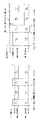
- Patent Document 1 has a configuration in which the power supply voltage of the P-channel MOSFET drive circuit is supplied from the drive voltage Vdrv. Therefore, as shown in FIG. 11 (1), when the output voltage Vo is lower than the drive voltage Vdrv, it is used for synchronous rectification. The P-channel MOSFET can be driven on and off. However, as shown in FIG. 11 (2), when the output voltage Vo is set higher than the drive voltage Vdrv, the first drive signal switches from Low to High at the timing of T2b and exceeds the threshold value Vth_Nch of the N channel MOSFET3. The N-channel MOSFET 3 switches from off to on.
- Patent Document 2 discloses a configuration in which a drive voltage of a synchronous rectification P-channel MOSFET is supplied from between an output voltage and GND.
- the drive circuit of the synchronous rectification P-channel MOSFET can be simplified, and an output voltage Vo higher than the drive voltage of the drive circuit can be generated.
- the off-drive side of the output stage circuit of the drive means of the synchronous rectification P-channel MOSFET is composed of a resistor, it is difficult to discharge the gate-source capacitance Cgs of the synchronous rectification P-channel MOSFET at high speed, and it is used in vehicles. There is a problem that it is difficult to cope with high-speed switching operation at, for example, 2 MHz or higher, which is required in.
- the lower the on-resistance value of the P-channel MOSFET the larger the gate-source capacitance Cgs tends to be. Therefore, when a large output current is supplied, the gate-source capacitance Cgs becomes large and the switching loss increases. Even if the gate resistance is reduced to accelerate the switching operation, the loss of the gate resistance becomes excessive this time, and high-speed switching operation becomes difficult.
- the output voltage set value determines the power supply voltage value of the driver IC.
- a sufficient drive voltage cannot be supplied, which causes a problem that the P-channel MOSFET cannot be driven off.
- a drive voltage switching means of a drive circuit for driving a synchronous rectification MOS transistor is provided.
- the drive voltage switching means switches the connection so that power is supplied from the output voltage to the drive circuit to the drive circuit, and power is supplied to the drive circuit.
- the connection is switched so as to supply power from the drive voltage.
- the present invention it is possible to secure a power source for driving a MOS transistor for synchronous rectification by switching and connecting to a higher voltage of either the drive voltage or the output voltage. As a result, the P-channel MOSFET can be reliably driven off.
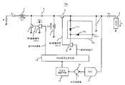
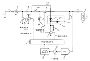
- FIG. 1 is a diagram showing a DC / DC converter configured by the SEPIC circuit according to the first embodiment of the present invention.
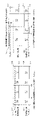
- FIG. 2 is a diagram showing a first drive signal and a second drive signal depending on the voltage magnitude relationship between the drive voltage and the output voltage in the first embodiment of the present invention shown in FIG.
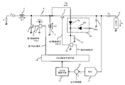
- FIG. 3 is a diagram showing a DC / DC converter configured by the SEPIC circuit according to the second embodiment of the present invention.
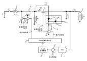
- FIG. 4 is a diagram showing a DC / DC converter configured by the SEPIC circuit according to the third embodiment of the present invention.
- FIG. 5 is a diagram showing a DC / DC converter configured by the SEPIC circuit according to the fourth embodiment of the present invention.
- FIG. 1 is a diagram showing a DC / DC converter configured by the SEPIC circuit according to the first embodiment of the present invention.
- FIG. 2 is a diagram showing a first drive signal and a second drive signal depending on the voltage magnitude relationship between the drive voltage and the output voltage in the first embodiment
- FIG. 6 is a diagram showing a first drive signal and a second drive signal when the output voltage Vo is higher than the drive voltage Vdrv in the fourth embodiment of the present invention shown in FIG.
- FIG. 7 is a diagram showing operation waveforms of each part when the output voltage Vo is higher than the drive voltage Vdrv in the fourth embodiment of the present invention shown in FIG.
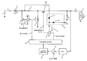
- FIG. 8 is a diagram showing a DC / DC converter configured by the SEPIC circuit according to the fifth embodiment of the present invention.
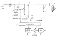
- FIG. 9 is a diagram showing a DC / DC converter configured by the SEPIC circuit according to the sixth embodiment of the present invention.
- FIG. 10 is a diagram showing a SEPIC circuit of the prior art.
- FIG. 11 is a diagram showing a first drive signal and a second drive signal depending on the voltage magnitude relationship between the drive voltage and the output voltage in the prior art shown in FIG.
- the first inductor 2 In the first embodiment of FIG. 1, the first inductor 2, the N channel MOSFET 3, the coupling capacitor 4, the second inductor 5, the P channel MOSFET 6, the output capacitor 7, the output load 8, the first drive means 9, and the second drive means are shown. It is composed of 10, an AD converter 11, a subtractor 12, a filter calculation means 13, a PWM signal generation means 14, and a drive voltage switching unit 15. Further, the drive voltage switching unit 15 is composed of a switch means 16, a switch means 17, and a voltage switching control means 18, and the voltage switching control means 18 compares the output voltage Vo and the drive voltage Vdrv, and the output voltage Vo is determined. When the drive voltage is lower than Vdrv, the switch means 16 is turned on and the switch means 17 is turned off.
- the second driving means 10 drives the P channel MOSFET 6 at the driving voltage Vdrv.
- the switch means 16 is turned off and the switch means 17 is turned on.
- the second driving means 10 drives the P channel MOSFET 4 with the output voltage Vo.
- a drive voltage Vdrv is supplied to the power supply terminal of the first drive means 1, and the N-channel MOSFET 3 is driven based on the first PWM signal output from the PWM signal generation means.
- the gate threshold voltage Vth_Nch is not affected by the output voltage Vo.
- a drive voltage Vdrv or an output voltage Vo is supplied to the power supply terminal of the second drive means 10 via the drive voltage switching unit 15, and the P channel MOSFET 6 is driven based on the second PWM signal.
- the output voltage Vo is generated by supplying the excited energy to the output capacitor 7 and the output load 8.
- the AD converter 11 detects the output voltage Vo, converts it into a digital value having a predetermined number of bits, and outputs the digital conversion value to the subtractor 12.
- the subtractor 12 generates a difference value between the output target value and the digital conversion value, and outputs the difference value to the filter calculation means 13.
- the filter calculation means 13 performs PI or PID calculation based on the difference value, and outputs the calculated value to the PWM signal generation means 14.
- the PWM signal generation means 14 generates a first PWM signal and a second PWM signal having a duty according to the calculated value.
- the first drive signal switches from High to Low and falls below the threshold value Vth_Nch of the N-channel MOSFET 2, so that the N-channel MOSFET 2 is switched from on to off. Further, since the second drive signal is switched from High to Low and falls below the threshold value Vth_Pch (GND reference) of the P channel MOSFET 6, the P channel MOSFET 4 is switched from off to on. At the timing of T2a, the first drive signal is switched from Low to High and the threshold value Vth_Nch of the N-channel MOSFET 3 is exceeded, so that the N-channel MOSFET 3 is switched from off to on.
- the second drive signal is switched from Low to High and exceeds the threshold value Vth_Pch (GND reference) of the P channel MOSFET 6, the P channel MOSFET 6 is switched from on to off.
- the output voltage Vo is set higher than the drive voltage Vdrv
- the drive voltage Vdrv is supplied to the power supply voltage of the first drive means
- the power supply voltage of the second drive means 10 is the switch means of the drive voltage switching unit 15.
- the output voltage Vo is supplied via 17.
- the first drive signal switches from High to Low and falls below the threshold value Vth_Nch of the N-channel MOSFET 3, so that the N-channel MOSFET 3 switches from on to off.
- the second drive signal is switched from High to Low and falls below the threshold value Vth_Pch (GND reference) of the P channel MOSFET 6, the P channel MOSFET 6 is switched from off to on.
- the first drive signal switches from Low to High and exceeds the threshold value Vth_Nch of the N-channel MOSFET 2, so that the N-channel MOSFET 2 is switched from off to on.
- the second drive signal is switched from Low to High and exceeds the threshold value Vth_Pch (GND reference) of the P channel MOSFET 6, the P channel MOSFET 6 is switched from on to off.
- the optimum power supply voltage can be supplied to the second drive means regardless of the output voltage value, a highly efficient power supply circuit can be configured in a wide output voltage range.
- high speed is possible because a general push-pull output driver IC in which the output stage circuit is composed of a combination of a P-channel MOSFET and an N-channel MOSFET can be used as the second drive means. It can handle operations, and can also support switching operations of 2 MHz or higher, which are required for in-vehicle applications. Further, it is also possible to realize cost reduction by integrating the second drive means 10 and the drive voltage switching means 15 on the same semiconductor substrate. Further, if an element in which the inductor 2 and the inductor 5 are made of one core material is used, the effect of integration of mounting and cost reduction can be further obtained.
- the second embodiment shown in FIG. 3 is different from the first embodiment shown in FIG. 1 in that the drive voltage switching means 15 is changed to 15a.
- the drive voltage switching means 15a is composed of a cathode common connection between the diode 16a and the diode 17a.
- the drive voltage switching means 15a is composed of an or circuit of the diode 16a and the diode 17a, compares the output voltage Vo and the drive voltage Vdrv, and when the output voltage Vo is lower than the drive voltage Vdrv, the second from the diode 16a to the second.
- the drive voltage Vdrv is supplied to the power supply terminal of the drive means 10.
- the P channel MOSFET 6 is driven by the drive voltage Vdrv.
- the output voltage Vo exceeds the drive voltage Vdrv
- the output voltage Vo is supplied from the diode 17a to the power supply terminal of the second drive means 10.
- the P channel MOSFET 6 is driven by the output voltage Vo.
- the second embodiment is configured to drive the P channel MOSFET 6 via the diode 16a or 17a, and a voltage drop occurs due to the forward voltage VF of the diode. Therefore, it is preferable to use a Schottky diode having a low forward voltage. ..
- the third embodiment shown in FIG. 4 is a change from the drive voltage switching means 15a to 15b with respect to the second embodiment of FIG. 3, and is a change of the anode connection portion of the diode 17b configured in the drive voltage switching means 15b.
- the anode of the diode 17b is connected to the drain of the P channel MOSFET 6 and the connection point of the inductance 5 and the capacitor 4, and the cathode is connected to the drive voltage Vdrv in an ore connection to obtain a drive voltage higher than that of the second embodiment. Can be generated.
- the diode 17b is higher than that of the second embodiment.
- the voltage supplied to the power supply terminal of the second drive means 10 can be supplied higher by the on-voltage between the drain and the source of the P channel MOSFET 6. Therefore, the gate terminal voltage of the P channel MOSFET 6 at the time of off becomes higher than that of the third embodiment, and the gate terminal capacity can be charged more quickly, so that the P channel MOSFET 6 can be turned off at high speed.
- the fourth embodiment shown in FIG. 5 is changed from the drive voltage switching means 15b to 15c with respect to the third embodiment of FIG. 4, and has an inductance 5, a capacitor 4, a connection point with the diode 17c anode, and a drain terminal of the P channel MOSFET 6.
- the difference is that a third inductor 20c is added in between.
- the third inductor 20c may be an inductor having a small inductance value such as ferrite beads, and may be replaced by the inductance of the board wiring or the like.
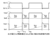
- FIG. 6 shows a first drive signal and a second drive signal when the output voltage Vo is higher than the drive voltage Vdrv.
- FIG. 7 is an operation waveform diagram of the N-channel MOSFET 3, the P-channel MOSFET 6, and the diode D17c under the same conditions.
- the drive voltage switching means 15c is changed to 15d with respect to the fourth embodiment of FIG. 5, and the insertion point of the third inductor 20d is the capacitor 4, the second inductor 5, and the P channel MOSFET 6.
- the difference is that it is inserted between the drain terminal connection points of.
- the anode of the diode 17d of the drive voltage switching means 15d is connected to the connection point between the capacitor 4 and the second inductor 5.
- the third inductor 20d may be an inductor having a small inductance value such as ferrite beads, or may be replaced by an inductance of the board wiring or the like.
- the high side voltage of the drive output of the second drive means 10 can be set higher than the output voltage Vo, so that the same effect as that of the fourth embodiment can be obtained. Be done.
- the drive voltage switching means 15 is changed to 15e with respect to the second embodiment of FIG. 3, and the anode terminal of the diode 17e of the drive voltage switching means 15e is connected to the output voltage Vo connection to the inductance 3
- the pulse voltage value of the anode terminal voltage of the diode 17e is the sum of the input voltage Vi and the output voltage Vo
- the voltage of the second drive signal of the P channel MOSFET 6 can be supplied as high as the input voltage Vi. Therefore, the gate terminal voltage of the P-channel MOSFET 6 at the time of off can be made higher than the output voltage VO, and the gate terminal capacity can be charged quickly, so that the P-channel MOSFET 6 can be turned off at high speed.
- the drive power supply according to the present invention is suitable for use as a drive power source for a synchronous rectifying element of a SEPIC converter. Therefore, it can be used as a power source for an in-vehicle device using this.
Landscapes
- Engineering & Computer Science (AREA)
- Power Engineering (AREA)
- Dc-Dc Converters (AREA)
Abstract
同期整流型SEPIC回路で構成されたDC-DCコンバータの駆動用電源を安定供給する。 【解決手段】 インダクタ2、5、スイッチング素子3、コンデンサ4、同期整流素子6、出力コンデンサ7で構成された同期整流型SEPIC回路1において、出力電圧Voと同期整流素子6の駆動電源電圧Vdrvの大小関係に関わらず、同期整流素子6の駆動信号電圧を安定に供給するための駆動電圧切替部15を備える。駆動電圧切替部15は、出力電圧Voが駆動電源電圧Vdrvより高い設定では、出力電圧Voから第2駆動回路10へ電源供給するように接続切替し、出力電圧Voが駆動電圧Vdrvより低い設定時は駆動電圧Vdrvから電源供給するように接続切替する手段を備えたことを特徴とする。
Description
本発明は、SEPIC回路で構成されたDC/DCコンバータに関する。
自動車のバッテリーなどの不安定な入力電源から安定した出力電圧を生成する手段として、昇降圧コンバータが使用されている。バッテリーの無駄な消耗を抑えるには電源回路の高効率化が必要であるが、図10に示すように、整流手段にPチャネルMOSFETを用いることで損失低減を実現した同期整流型SEPIC回路で構成されたDC-DCコンバータが、特許文献1、2に開示されている。
特許文献1は、PチャネルMOSFET駆動回路の電源電圧を駆動電圧Vdrvから供給する構成のため、図11(1)に示すように、出力電圧Voが駆動電圧Vdrvより低い場合には、同期整流用PチャネルMOSFETをオンオフ駆動できる。
しかし、図11(2)に示すように、出力電圧Voが駆動電圧Vdrvより高い設定では、T2bのタイミングで第1駆動信号がLowからHighに切り替わりNチャネルMOSFET3のしきい値Vth_Nchを上回るためにNチャネルMOSFET3はオフからオンに切り変わる。一方、第2駆動信号がLowからHighに切り替わるがPチャネルMOSFET6のしきい値Vth_Pch(GND基準)を上回ることができないためにPチャネルMOSFET6はオンからオフに切り変わらない。このために出力電圧Vo端子からPchMOSFET6と第2インダクタ5を介してGNDへ電流が逆流してしまい、出力電圧Voが駆動電圧Vdrvよりも上昇することができない。このために、出力電圧Voの設定を、駆動電圧Vdrvよりも低く制限しなければならない問題がある。
また、特許文献2には、同期整流用PチャネルMOSFETの駆動電圧を出力電圧とGND間から供給する構成が開示されている。これにより同期整流用PチャネルMOSFETの駆動回路を簡素化でき、駆動回路の駆動電圧よりも高い出力電圧Voを発生することができる。
しかし、同期整流用PチャネルMOSFETの駆動手段の出力段回路のオフ駆動側が抵抗で構成されているので、同期整流用PチャネルMOSFETのゲート―ソース間容量Cgsを高速に放電するが難しく、車載用途で求められる、例えば2MHz以上での高速なスイッチング動作への対応が困難な問題がある。その上、PチャネルMOSFETのオン抵抗値が低くなる程ゲート―ソース間容量Cgsは大きくなる傾向にある。
従って、大出力電流を供給する場合、ゲート―ソース間容量Cgsは大きくなり、スイッチング損失が増加する。仮にゲート抵抗を小さくしてスイッチング動作を早めたとしても、今度はゲート抵抗の損失が過大になってしまい、高速なスイッチング動作が困難になる。
しかし、図11(2)に示すように、出力電圧Voが駆動電圧Vdrvより高い設定では、T2bのタイミングで第1駆動信号がLowからHighに切り替わりNチャネルMOSFET3のしきい値Vth_Nchを上回るためにNチャネルMOSFET3はオフからオンに切り変わる。一方、第2駆動信号がLowからHighに切り替わるがPチャネルMOSFET6のしきい値Vth_Pch(GND基準)を上回ることができないためにPチャネルMOSFET6はオンからオフに切り変わらない。このために出力電圧Vo端子からPchMOSFET6と第2インダクタ5を介してGNDへ電流が逆流してしまい、出力電圧Voが駆動電圧Vdrvよりも上昇することができない。このために、出力電圧Voの設定を、駆動電圧Vdrvよりも低く制限しなければならない問題がある。
また、特許文献2には、同期整流用PチャネルMOSFETの駆動電圧を出力電圧とGND間から供給する構成が開示されている。これにより同期整流用PチャネルMOSFETの駆動回路を簡素化でき、駆動回路の駆動電圧よりも高い出力電圧Voを発生することができる。
しかし、同期整流用PチャネルMOSFETの駆動手段の出力段回路のオフ駆動側が抵抗で構成されているので、同期整流用PチャネルMOSFETのゲート―ソース間容量Cgsを高速に放電するが難しく、車載用途で求められる、例えば2MHz以上での高速なスイッチング動作への対応が困難な問題がある。その上、PチャネルMOSFETのオン抵抗値が低くなる程ゲート―ソース間容量Cgsは大きくなる傾向にある。
従って、大出力電流を供給する場合、ゲート―ソース間容量Cgsは大きくなり、スイッチング損失が増加する。仮にゲート抵抗を小さくしてスイッチング動作を早めたとしても、今度はゲート抵抗の損失が過大になってしまい、高速なスイッチング動作が困難になる。
ここで、駆動手段に一般的なドライバIC(出力段がPチャネルMOSFETとNチャネルMOSFETの組み合わせで構成されたプッシュプル構成)を用いた場合でも、出力電圧設定値がドライバICの電源電圧値を上回る条件では十分な駆動電圧を供給できず、PチャネルMOSFETをオフ駆動できない問題を生じる。
上記問題に鑑み、本発明は、出力電圧設定範囲によらずSEPIC回路の同期整流用PチャネルMOSFETを制御できる駆動用電源を提供することを課題とする。
上記課題を解決するために、本発明の一態様によれば、同期整流型SEPICであるDC-DCコンバータにおいて、同期整流用MOSトランジスタを駆動するための駆動回路の駆動電圧切替手段を備え、前記駆動電圧切替手段は、前記駆動回路へ電源供給するための駆動電圧が出力電圧より低い設定時に、前記駆動回路へ出力電圧から前記駆動回路へ電源供給するように接続切替し、前記駆動回路へ電源供給するための駆動電圧が出力電圧より高い設定時は、駆動電圧から電源供給するように接続切替する手段を備えたことを特徴とする。
本発明によると、駆動電圧と出力電圧のいずれかの高い電圧に切り替えて接続することで、同期整流用MOSトランジスタを駆動するための電源を確保することが可能になる。これにより、PチャネルMOSFETを確実にオフ駆動することができる。
(実施形態1)
図1の第1実施例は、第1インダクタ2、NチャネルMOSFET3、カップリングコンデンサ4、第2インダクタ5、PチャネルMOSFET6、出力コンデンサ7、出力負荷8、第1駆動手段9、第2駆動手段10、ADコンバータ11、減算器12、フィルタ演算手段13、PWM信号生成手段14、駆動電圧切替部15で構成されている。
また、駆動電圧切替部15は、スイッチ手段16、スイッチ手段17、および電圧切替制御手段18とで構成され、電圧切替制御手段18にて出力電圧Voと駆動電圧Vdrvを比較し、出力電圧Voが駆動電圧Vdrvを下回っている場合にはスイッチ手段16をオン、スイッチ手段17をオフにする。これによって、第2駆動手段10はPチャネルMOSFET6を駆動電圧Vdrvで駆動する。
また、出力電圧Voが駆動電圧Vdrvを上回っている場合にはスイッチ手段16をオフ、スイッチ手段17をオンにする。これによって、第2駆動手段10はPチャネルMOSFET4を出力電圧Voで駆動する。
なお、第1駆動手段1の電源端子には、駆動電圧Vdrvが供給され、PWM信号生成手段から出力される第1PWM信号を基にNチャネルMOSFET3を駆動する。ここで、NチャネルMOSFET3のソースはGND側に接続されるため、ゲート閾値電圧Vth_Nchは出力電圧Voに影響されない。
第2駆動手段10の電源端子には、駆動電圧切替部15を介して駆動電圧Vdrvまたは出力電圧Voの電圧が供給され、第2PWM信号を基にPチャネルMOSFET6を駆動する。
NチャネルMOSFET3がオン、且つ、PチャネルMOSET6がオフの期間に、第1インダクタ2と第2インダクタ5にエネルギーを励磁して、NチャネルMOSFET3がオフ、且つ、PチャネルMOSFET6がオンの期間に、励磁されたエネルギーを出力コンデンサ7と出力負荷8に対して供給することで出力電圧Voを発生する。
ADコンバータ11は、出力電圧Voを検出し、所定のビット数のデジタル値に変換し、デジタル変換値を減算器12に出力する。
減算器12は、出力目標値とデジタル変換値の差分値を発生し、フィルタ演算手段13に出力する。フィルタ演算手段13は、差分値を基にPIやPID演算を行い、演算値をPWM信号生成手段14へ出力する。
PWM信号生成手段14は演算値に応じたデュティーを持つ第1PWM信号と、第2PWM信号を生成する。
図1の第1実施例は、第1インダクタ2、NチャネルMOSFET3、カップリングコンデンサ4、第2インダクタ5、PチャネルMOSFET6、出力コンデンサ7、出力負荷8、第1駆動手段9、第2駆動手段10、ADコンバータ11、減算器12、フィルタ演算手段13、PWM信号生成手段14、駆動電圧切替部15で構成されている。
また、駆動電圧切替部15は、スイッチ手段16、スイッチ手段17、および電圧切替制御手段18とで構成され、電圧切替制御手段18にて出力電圧Voと駆動電圧Vdrvを比較し、出力電圧Voが駆動電圧Vdrvを下回っている場合にはスイッチ手段16をオン、スイッチ手段17をオフにする。これによって、第2駆動手段10はPチャネルMOSFET6を駆動電圧Vdrvで駆動する。
また、出力電圧Voが駆動電圧Vdrvを上回っている場合にはスイッチ手段16をオフ、スイッチ手段17をオンにする。これによって、第2駆動手段10はPチャネルMOSFET4を出力電圧Voで駆動する。
なお、第1駆動手段1の電源端子には、駆動電圧Vdrvが供給され、PWM信号生成手段から出力される第1PWM信号を基にNチャネルMOSFET3を駆動する。ここで、NチャネルMOSFET3のソースはGND側に接続されるため、ゲート閾値電圧Vth_Nchは出力電圧Voに影響されない。
第2駆動手段10の電源端子には、駆動電圧切替部15を介して駆動電圧Vdrvまたは出力電圧Voの電圧が供給され、第2PWM信号を基にPチャネルMOSFET6を駆動する。
NチャネルMOSFET3がオン、且つ、PチャネルMOSET6がオフの期間に、第1インダクタ2と第2インダクタ5にエネルギーを励磁して、NチャネルMOSFET3がオフ、且つ、PチャネルMOSFET6がオンの期間に、励磁されたエネルギーを出力コンデンサ7と出力負荷8に対して供給することで出力電圧Voを発生する。
ADコンバータ11は、出力電圧Voを検出し、所定のビット数のデジタル値に変換し、デジタル変換値を減算器12に出力する。
減算器12は、出力目標値とデジタル変換値の差分値を発生し、フィルタ演算手段13に出力する。フィルタ演算手段13は、差分値を基にPIやPID演算を行い、演算値をPWM信号生成手段14へ出力する。
PWM信号生成手段14は演算値に応じたデュティーを持つ第1PWM信号と、第2PWM信号を生成する。
次に、駆動電圧と出力電圧との電圧大小関係による第1駆動信号と第2駆動信号を示す図2のタイミングチャートを参照しながら詳細な全体動作を説明する。
ここで、第1インダクタ2と第2インダクタ5には、ほぼ等しいインダクタ値が選定されているものと仮定する。出力電圧Voの設定が駆動電圧Vdrvより低い場合は、第1駆動手段9の電源電圧には駆動電圧Vdrvが供給され、第2駆動手段10の電源電圧には駆動電圧切替部15のスイッチ手段16を介して駆動電圧Vdrvが供給される。
T1aのタイミングで第1駆動信号がHighからLowに切り替わりNチャネルMOSFET2のしきい値Vth_Nchを下回るためにNチャネルMOSFET2はオンからオフに切り変わる。また、第2駆動信号がHighからLowに切り替わりPチャネルMOSFET6のしきい値Vth_Pch(GND基準)を下回るためにPチャネルMOSFET4はオフからオンに切り変わる。
T2aのタイミングで第1駆動信号がLowからHighに切り替わりNチャネルMOSFET3のしきい値Vth_Nchを上回るためにNチャネルMOSFET3はオフからオンに切り変わる。また、第2駆動信号がLowからHighに切り替わりPチャネルMOSFET6のしきい値Vth_Pch(GND基準)を上回るためにPチャネルMOSFET6はオンからオフに切り変わる。
一方で出力電圧Voの設定が駆動電圧Vdrvより高い場合は、第1駆動手段の電源電圧には駆動電圧Vdrvが供給され、第2駆動手段10の電源電圧には駆動電圧切替部15のスイッチ手段17を介して出力電圧Voが供給される。
T1bのタイミングで第1駆動信号がHighからLowに切り替わりNチャネルMOSFET3のしきい値Vth_Nchを下回るためにNチャネルMOSFET3はオンからオフに切り変わる。また、第2駆動信号がHighからLowに切り替わりPチャネルMOSFET6のしきい値Vth_Pch(GND基準)を下回るためにPチャネルMOSFET6はオフからオンに切り変わる。
T2bのタイミングで第1駆動信号がLowからHighに切り替わりNチャネルMOSFET2のしきい値Vth_Nchを上回るためにNチャネルMOSFET2はオフからオンに切り変わる。また、第2駆動信号がLowからHighに切り替わりPチャネルMOSFET6のしきい値Vth_Pch(GND基準)を上回るためにPチャネルMOSFET6はオンからオフに切り変わる。
このように、先行技術1に対しては、出力電圧値に依らず最適な電源電圧を第2駆動手段に供給できるために広い出力電圧範囲で高効率な電源回路を構成できる。
また、先行技術2に対しては、第2駆動手段に出力段回路がPチャネルMOSFETとNチャネルMOSFETの組み合わせで構成されたプッシュプル出力の一般的なドライバICを用いることができるために高速な動作に対応でき、車載用途で求められる2MHz以上のスイッチング動作にも対応することができる。
また、第2駆動手段10と駆動電圧切替手段15を同一の半導体基板上に集積化することでコストダウンを実現することも可能である。さらに、インダクタ2とインダクタ5が一つのコア材で構成された素子を用いれば実装の集積化とコストダウンの効果をより得ることができる。
ここで、第1インダクタ2と第2インダクタ5には、ほぼ等しいインダクタ値が選定されているものと仮定する。出力電圧Voの設定が駆動電圧Vdrvより低い場合は、第1駆動手段9の電源電圧には駆動電圧Vdrvが供給され、第2駆動手段10の電源電圧には駆動電圧切替部15のスイッチ手段16を介して駆動電圧Vdrvが供給される。
T1aのタイミングで第1駆動信号がHighからLowに切り替わりNチャネルMOSFET2のしきい値Vth_Nchを下回るためにNチャネルMOSFET2はオンからオフに切り変わる。また、第2駆動信号がHighからLowに切り替わりPチャネルMOSFET6のしきい値Vth_Pch(GND基準)を下回るためにPチャネルMOSFET4はオフからオンに切り変わる。
T2aのタイミングで第1駆動信号がLowからHighに切り替わりNチャネルMOSFET3のしきい値Vth_Nchを上回るためにNチャネルMOSFET3はオフからオンに切り変わる。また、第2駆動信号がLowからHighに切り替わりPチャネルMOSFET6のしきい値Vth_Pch(GND基準)を上回るためにPチャネルMOSFET6はオンからオフに切り変わる。
一方で出力電圧Voの設定が駆動電圧Vdrvより高い場合は、第1駆動手段の電源電圧には駆動電圧Vdrvが供給され、第2駆動手段10の電源電圧には駆動電圧切替部15のスイッチ手段17を介して出力電圧Voが供給される。
T1bのタイミングで第1駆動信号がHighからLowに切り替わりNチャネルMOSFET3のしきい値Vth_Nchを下回るためにNチャネルMOSFET3はオンからオフに切り変わる。また、第2駆動信号がHighからLowに切り替わりPチャネルMOSFET6のしきい値Vth_Pch(GND基準)を下回るためにPチャネルMOSFET6はオフからオンに切り変わる。
T2bのタイミングで第1駆動信号がLowからHighに切り替わりNチャネルMOSFET2のしきい値Vth_Nchを上回るためにNチャネルMOSFET2はオフからオンに切り変わる。また、第2駆動信号がLowからHighに切り替わりPチャネルMOSFET6のしきい値Vth_Pch(GND基準)を上回るためにPチャネルMOSFET6はオンからオフに切り変わる。
このように、先行技術1に対しては、出力電圧値に依らず最適な電源電圧を第2駆動手段に供給できるために広い出力電圧範囲で高効率な電源回路を構成できる。
また、先行技術2に対しては、第2駆動手段に出力段回路がPチャネルMOSFETとNチャネルMOSFETの組み合わせで構成されたプッシュプル出力の一般的なドライバICを用いることができるために高速な動作に対応でき、車載用途で求められる2MHz以上のスイッチング動作にも対応することができる。
また、第2駆動手段10と駆動電圧切替手段15を同一の半導体基板上に集積化することでコストダウンを実現することも可能である。さらに、インダクタ2とインダクタ5が一つのコア材で構成された素子を用いれば実装の集積化とコストダウンの効果をより得ることができる。
(実施形態2)
図3に示す実施形態2は、図1の実施形態1に対して駆動電圧切替手段15から15aに変更になっているところが相違点である。駆動電圧切替手段15aはダイオード16aとダイオード17aとのカソードコモン接続で構成されている。
駆動電圧切替手段15aは、ダイオード16aとダイオード17aとのオア回路から構成され、出力電圧Voと駆動電圧Vdrvを比較し、出力電圧Voが駆動電圧Vdrvを下回っている場合にはダイオード16aから第2駆動手段10の電源端子に対し駆動電圧Vdrvが供給される。これによって、PチャネルMOSFET6を駆動電圧Vdrvで駆動する。
また、出力電圧Voが駆動電圧Vdrvを上回っている場合にはダイオード17aから第2駆動手段10の電源端子に対し出力電圧Voが供給される。これによって、PチャネルMOSFET6を出力電圧Voで駆動する。
実施形態2はダイオード16aまたは17aを介してPチャネルMOSFET6を駆動する構成であり、ダイオードの順方向電圧VFによる電圧降下が発生するため、低順方向電圧のショットキーダイオードなどを使用することが好ましい。
図3に示す実施形態2は、図1の実施形態1に対して駆動電圧切替手段15から15aに変更になっているところが相違点である。駆動電圧切替手段15aはダイオード16aとダイオード17aとのカソードコモン接続で構成されている。
駆動電圧切替手段15aは、ダイオード16aとダイオード17aとのオア回路から構成され、出力電圧Voと駆動電圧Vdrvを比較し、出力電圧Voが駆動電圧Vdrvを下回っている場合にはダイオード16aから第2駆動手段10の電源端子に対し駆動電圧Vdrvが供給される。これによって、PチャネルMOSFET6を駆動電圧Vdrvで駆動する。
また、出力電圧Voが駆動電圧Vdrvを上回っている場合にはダイオード17aから第2駆動手段10の電源端子に対し出力電圧Voが供給される。これによって、PチャネルMOSFET6を出力電圧Voで駆動する。
実施形態2はダイオード16aまたは17aを介してPチャネルMOSFET6を駆動する構成であり、ダイオードの順方向電圧VFによる電圧降下が発生するため、低順方向電圧のショットキーダイオードなどを使用することが好ましい。
(実施形態3)
図4に示す実施形態3は、図3の実施形態2に対して駆動電圧切替手段15aから15bに変更であり、駆動電圧切替手段15bに構成されているダイオード17bのアノード接続箇所の変更になっているところが相違点である。
実施形態3は、PチャネルMOSFET6のドレインとインダクタンス5、コンデンサ4の接続点にダイオード17bのアノードを接続し、カソードを駆動電圧Vdrvとオア接続にすることで、実施形態2よりも高い駆動電圧を生成できる。
PチャネルMOSFET6がオン動作している時のドレイン~ソース間の電圧降下が出力電圧Voに加算されるため、出力電圧Voが駆動電圧Vdrvを上回っている場合には、実施形態2よりもダイオード17bから第2駆動手段10の電源端子に対し供給される電圧が、PチャネルMOSFET6のドレイン~ソース間のオン電圧分だけ高く供給できる効果がある。このため、オフ時のPチャネルMOSFET6のゲート端子電圧が、実施形態3よりも高くなり、ゲート端子容量をよりすばやく充電できるのでPチャネルMOSFET6を高速にオフすることが可能となる。
図4に示す実施形態3は、図3の実施形態2に対して駆動電圧切替手段15aから15bに変更であり、駆動電圧切替手段15bに構成されているダイオード17bのアノード接続箇所の変更になっているところが相違点である。
実施形態3は、PチャネルMOSFET6のドレインとインダクタンス5、コンデンサ4の接続点にダイオード17bのアノードを接続し、カソードを駆動電圧Vdrvとオア接続にすることで、実施形態2よりも高い駆動電圧を生成できる。
PチャネルMOSFET6がオン動作している時のドレイン~ソース間の電圧降下が出力電圧Voに加算されるため、出力電圧Voが駆動電圧Vdrvを上回っている場合には、実施形態2よりもダイオード17bから第2駆動手段10の電源端子に対し供給される電圧が、PチャネルMOSFET6のドレイン~ソース間のオン電圧分だけ高く供給できる効果がある。このため、オフ時のPチャネルMOSFET6のゲート端子電圧が、実施形態3よりも高くなり、ゲート端子容量をよりすばやく充電できるのでPチャネルMOSFET6を高速にオフすることが可能となる。
(実施形態4)
図5に示す実施形態4は、図4の実施形態3に対して駆動電圧切替手段15bから15cに変更になり、インダクタンス5、コンデンサ4、ダイオード17cアノードとの接続点とPチャネルMOSFET6のドレイン端子間に、第3インダクタ20cを追加しているところが相違点である。ここで、第3インダクタ20cはフェライトビーズなどのインダクタンス値の小さいインダクタでよく、基板配線のインダクタンスなどで代替えしてもよい。
実施形態4では、PチャネルMOSFET6と直列にインダクタ20cを接続することで、第2駆動手段10の駆動出力のHigh側電圧を出力電圧Voより高く設定できるため、実施例3より高速なスイッチングが実現でき、より高効率な電源が構成できる。
図6は、出力電圧Voが駆動電圧Vdrvより高い場合の第1駆動信号と第2駆動信号を示す。図7は、同条件でのNチャネルMOSFET3、PチャネルMOSFET6、ダイオードD17cの動作波形図である。
図7に示す時刻T1cにてPチャネルMOSFET6がターンオフ、PチャネルMOSFET6がターンオンするとインダクタ20cに起電力が生じ、時刻T1´cの期間までダイオード17cを介してコンデンサ19に充電電流が流れる。これにより、図6に示すように、PチャネルMOSFET6の第2駆動信号のHigh側電圧を第3インダクタ20cによる充電電圧分だけ高く供給できる効果がある。このため、PチャネルMOSFET6のゲート端子容量をすばやく充電でき、PチャネルMOSFET6を高速にオフすることが可能となる。
図5に示す実施形態4は、図4の実施形態3に対して駆動電圧切替手段15bから15cに変更になり、インダクタンス5、コンデンサ4、ダイオード17cアノードとの接続点とPチャネルMOSFET6のドレイン端子間に、第3インダクタ20cを追加しているところが相違点である。ここで、第3インダクタ20cはフェライトビーズなどのインダクタンス値の小さいインダクタでよく、基板配線のインダクタンスなどで代替えしてもよい。
実施形態4では、PチャネルMOSFET6と直列にインダクタ20cを接続することで、第2駆動手段10の駆動出力のHigh側電圧を出力電圧Voより高く設定できるため、実施例3より高速なスイッチングが実現でき、より高効率な電源が構成できる。
図6は、出力電圧Voが駆動電圧Vdrvより高い場合の第1駆動信号と第2駆動信号を示す。図7は、同条件でのNチャネルMOSFET3、PチャネルMOSFET6、ダイオードD17cの動作波形図である。
図7に示す時刻T1cにてPチャネルMOSFET6がターンオフ、PチャネルMOSFET6がターンオンするとインダクタ20cに起電力が生じ、時刻T1´cの期間までダイオード17cを介してコンデンサ19に充電電流が流れる。これにより、図6に示すように、PチャネルMOSFET6の第2駆動信号のHigh側電圧を第3インダクタ20cによる充電電圧分だけ高く供給できる効果がある。このため、PチャネルMOSFET6のゲート端子容量をすばやく充電でき、PチャネルMOSFET6を高速にオフすることが可能となる。
(実施形態5)
図8に示す実施形態5は、図5の実施形態4に対して駆動電圧切替手段15cから15dに変更になり、第3インダクタ20dの挿入個所をコンデンサ4と、第2インダクタ5とPチャネルMOSFET6のドレイン端子接続点の間に挿入したところが相違点である。また、駆動電圧切替手段15dのダイオード17dのアノードは、コンデンサ4と第2インダクタ5との接続点に接続される。ここで、実施形態4と同様に、第3インダクタ20dはフェライトビーズなどのインダクタンス値の小さいインダクタでもよく、基板配線のインダクタンスなどで代替えしてもよい。
実施形態5では、PチャネルMOSFET6と直列にインダクタ20dを接続することで、第2駆動手段10の駆動出力のHigh側電圧を出力電圧Voより高く設定できるため、実施例4と同等の効果を得られる。
図8に示す実施形態5は、図5の実施形態4に対して駆動電圧切替手段15cから15dに変更になり、第3インダクタ20dの挿入個所をコンデンサ4と、第2インダクタ5とPチャネルMOSFET6のドレイン端子接続点の間に挿入したところが相違点である。また、駆動電圧切替手段15dのダイオード17dのアノードは、コンデンサ4と第2インダクタ5との接続点に接続される。ここで、実施形態4と同様に、第3インダクタ20dはフェライトビーズなどのインダクタンス値の小さいインダクタでもよく、基板配線のインダクタンスなどで代替えしてもよい。
実施形態5では、PチャネルMOSFET6と直列にインダクタ20dを接続することで、第2駆動手段10の駆動出力のHigh側電圧を出力電圧Voより高く設定できるため、実施例4と同等の効果を得られる。
(実施形態6)
図9に示す実施形態6は、図3の実施形態2に対して駆動電圧切替手段15から15eに変更になり、駆動電圧切替手段15eのダイオード17eのアノード端子を出力電圧Vo接続から、インダクタンス3、コンデンサ4、NチャネルMOSFET3のドレイン端子との接続点に変更しているところが相違点である。
ここで、ダイオード17eのアノード端子電圧のパルス電圧値は入力電圧Viと出力電圧Voの和になり、PチャネルMOSFET6の第2駆動信号の電圧を入力電圧Vi分だけ高く供給できる。このため、オフ時のPチャネルMOSFET6のゲート端子電圧を出力電圧VOよりも高くでき、すばやくゲート端子容量を充電できるためにPチャネルMOSFET6を高速にオフすることが可能となる。
図9に示す実施形態6は、図3の実施形態2に対して駆動電圧切替手段15から15eに変更になり、駆動電圧切替手段15eのダイオード17eのアノード端子を出力電圧Vo接続から、インダクタンス3、コンデンサ4、NチャネルMOSFET3のドレイン端子との接続点に変更しているところが相違点である。
ここで、ダイオード17eのアノード端子電圧のパルス電圧値は入力電圧Viと出力電圧Voの和になり、PチャネルMOSFET6の第2駆動信号の電圧を入力電圧Vi分だけ高く供給できる。このため、オフ時のPチャネルMOSFET6のゲート端子電圧を出力電圧VOよりも高くでき、すばやくゲート端子容量を充電できるためにPチャネルMOSFET6を高速にオフすることが可能となる。
以上、本発明の実施形態を説明したが、上記実施形態は、本発明の技術的思想を具体化するための例示であって、個々の構成、組合せ等を上記のものに特定するものではない。本発明は、要旨を逸脱しない範囲内で種々変更して実施できる。
以上のように、本発明に係る駆動用電源は、SEPICコンバータの同期整流素子の駆動用電源などに用いるのに好適である。従って、これを用いた車載装置の電源などに利用可能である。
1、1a、1b、1c、1d、1e SEPICコンバータ
2 第1インダクタ
3 NチャネルMOSFET
4 コンデンサ
5 第2インダクタ
6 PチャネルMOSFET
7 出力コンデンサ
8 負荷
9 第1駆動手段
10 第2駆動手段
11 ADコンバータ
12 減算器
13 フィルタ演算手段
14 PWM信号生成手段
15、15a、15b、15c、15d、15e 駆動電圧切替部
16、16a、16b、16c、16d、16e ダイオード
17、17a、17b、17c、17d、17e ダイオード
18 電圧切替制御手段
19 コンデンサ
20c、20d 第3インダクタ
2 第1インダクタ
3 NチャネルMOSFET
4 コンデンサ
5 第2インダクタ
6 PチャネルMOSFET
7 出力コンデンサ
8 負荷
9 第1駆動手段
10 第2駆動手段
11 ADコンバータ
12 減算器
13 フィルタ演算手段
14 PWM信号生成手段
15、15a、15b、15c、15d、15e 駆動電圧切替部
16、16a、16b、16c、16d、16e ダイオード
17、17a、17b、17c、17d、17e ダイオード
18 電圧切替制御手段
19 コンデンサ
20c、20d 第3インダクタ
Claims (7)
- 同期整流型SEPICであるDC-DCコンバータにおいて、
同期整流用MOSトランジスタを駆動するための駆動回路の駆動電圧切替手段を備え、
前記駆動電圧切替手段は、
前記駆動回路へ電源供給するための駆動電圧が出力電圧より低い設定時に、
前記駆動回路へ前記出力電圧から前記駆動回路へ電源供給するように接続切替し、
前記駆動回路へ電源供給するための駆動電圧が前記出力電圧より高い設定時は、前記駆動電圧から電源供給するように接続を切替える手段を備えたことを特徴とするDC-DCコンバータ。 - 入力電源とカップリングコンデンサの第1端子間に接続された第1インダクタと、
前記カップリングコンデンサの第1端子と接地間に接続された第1スイッチング素子と、
前記カップリングコンデンサの第2端子と前記接地間に接続された第2インダクタと、
前記カップリングコンデンサの第2端子と出力端子間に接続された第2スイッチング素子と、
前記第2スイッチング素子を駆動するための駆動手段と、
前記駆動手段へ電源供給するための駆動電圧と、を備えた同期整流型SEPIC回路で構成されたDC-DCコンバータにおいて、
前記駆動手段の駆動電圧切替手段を備え、
前記駆動電圧切替手段は、出力電圧が前記駆動電圧よりも高い設定に応じて、前記出力電圧または前記出力電圧より高い電圧源から前記駆動手段へ電源供給を行うように接続を切替え、前記出力電圧が前記駆動電圧よりも低い設定に応じて、前記駆動電圧から前記駆動手段へ電源供給を行うように接続を切替えることを特徴とするDC-DCコンバータ。 - 前記駆動電圧切替手段は、前記駆動電圧と前記駆動手段の間に接続された第1整流手段と、前記出力電圧と前記駆動手段の間に接続された第2整流手段を備えたことを特徴とする請求項1に記載のDC-DCコンバータ。
- 前記駆動電圧切替手段は、前記駆動電圧と前記駆動手段の間に接続された第1整流手段と、前記出力電圧と前記駆動手段の間に接続された第2整流手段を備え
前記第2整流手段は、前記カップリングコンデンサの第2端子と第2スイッチング素子との接続点に接続されることを特徴とする請求項2に記載のDC-DCコンバータ。 - 第3のインダクタと、前記第3のインダクタは、前記カップリングコンデンサの第2端子と接続された第2インダクタとの接続点と前記第2スイッチング素子との間に接続され、
前記第2整流手段は、前記カップリングコンデンサの第2端子と第2インダクタとの接続点に接続されることを特徴とする請求項2に記載のDC-DCコンバータ。 - 第3のインダクタと、前記第3のインダクタの一方は前記カップリングコンデンサの第2端子と接続され、他方は第2インダクタと前記第2スイッチング素子との接続点に接続され、
前記第2整流手段は、前記カップリングコンデンサの第2端子と第3インダクタとの接続点に接続されることを特徴とする請求項2に記載のDC-DCコンバータ。 - 前記駆動電圧切替手段は、前記駆動電圧と前記駆動手段の間に接続された第1整流手段と、
前記カップリングコンデンサの第1端子と第1スイッチング素子との接続点と前記駆動手段の間に接続された第2整流手段を備えたことを特徴とする請求項2に記載のDC-DCコンバータ。
Priority Applications (4)
| Application Number | Priority Date | Filing Date | Title |
|---|---|---|---|
| PCT/JP2020/047724 WO2022137292A1 (ja) | 2020-12-21 | 2020-12-21 | Sepicコンバータの同期整流素子の駆動用電源 |
| CN202080025518.4A CN114982112A (zh) | 2020-12-21 | 2020-12-21 | Sepic转换器的同步整流元件的驱动用电源 |
| JP2021561682A JP7647569B2 (ja) | 2020-12-21 | 2020-12-21 | Sepicコンバータの同期整流素子の駆動用電源 |
| US17/486,974 US12003180B2 (en) | 2020-12-21 | 2021-09-28 | Power supply for driving synchronous rectification elements of SEPIC converter |
Applications Claiming Priority (1)
| Application Number | Priority Date | Filing Date | Title |
|---|---|---|---|
| PCT/JP2020/047724 WO2022137292A1 (ja) | 2020-12-21 | 2020-12-21 | Sepicコンバータの同期整流素子の駆動用電源 |
Related Child Applications (1)
| Application Number | Title | Priority Date | Filing Date |
|---|---|---|---|
| US17/486,974 Continuation US12003180B2 (en) | 2020-12-21 | 2021-09-28 | Power supply for driving synchronous rectification elements of SEPIC converter |
Publications (1)
| Publication Number | Publication Date |
|---|---|
| WO2022137292A1 true WO2022137292A1 (ja) | 2022-06-30 |
Family
ID=82021722
Family Applications (1)
| Application Number | Title | Priority Date | Filing Date |
|---|---|---|---|
| PCT/JP2020/047724 Ceased WO2022137292A1 (ja) | 2020-12-21 | 2020-12-21 | Sepicコンバータの同期整流素子の駆動用電源 |
Country Status (4)
| Country | Link |
|---|---|
| US (1) | US12003180B2 (ja) |
| JP (1) | JP7647569B2 (ja) |
| CN (1) | CN114982112A (ja) |
| WO (1) | WO2022137292A1 (ja) |
Families Citing this family (1)
| Publication number | Priority date | Publication date | Assignee | Title |
|---|---|---|---|---|
| CN117767767B (zh) * | 2024-02-22 | 2024-05-10 | 江苏展芯半导体技术股份有限公司 | 一种多路输出的辅助电源 |
Citations (2)
| Publication number | Priority date | Publication date | Assignee | Title |
|---|---|---|---|---|
| JP2017069180A (ja) * | 2015-09-28 | 2017-04-06 | 三菱電機株式会社 | 光源点灯装置及び照明器具 |
| JP2019058016A (ja) * | 2017-09-22 | 2019-04-11 | キヤノン株式会社 | 電源装置 |
Family Cites Families (8)
| Publication number | Priority date | Publication date | Assignee | Title |
|---|---|---|---|---|
| US7352158B2 (en) | 2005-05-06 | 2008-04-01 | Mobility Electronics, Inc. | SEPIC synchronous rectification |
| JP2008193866A (ja) * | 2007-02-07 | 2008-08-21 | Seiko Instruments Inc | 昇圧型スイッチングレギュレータ |
| JP5167733B2 (ja) * | 2007-09-06 | 2013-03-21 | 株式会社リコー | 昇圧型dc/dcコンバータ |
| CN102005919B (zh) * | 2009-09-02 | 2014-03-12 | 瑞萨集成电路设计(北京)有限公司 | 一种升压型dc-dc转换器及方法 |
| JP2014003814A (ja) * | 2012-06-19 | 2014-01-09 | Rohm Co Ltd | 電源装置、並びに、これを用いた車載機器及び車両 |
| JP5937442B2 (ja) * | 2012-07-06 | 2016-06-22 | 旭化成エレクトロニクス株式会社 | Dc−dcコンバータ |
| US10469065B2 (en) * | 2018-03-01 | 2019-11-05 | Dialog Semiconductor (Uk) Limited | Multi-level gate control for transistor devices |
| US11233390B2 (en) * | 2019-09-09 | 2022-01-25 | Apple Inc. | Transient power management circuit |
-
2020
- 2020-12-21 JP JP2021561682A patent/JP7647569B2/ja active Active
- 2020-12-21 WO PCT/JP2020/047724 patent/WO2022137292A1/ja not_active Ceased
- 2020-12-21 CN CN202080025518.4A patent/CN114982112A/zh active Pending
-
2021
- 2021-09-28 US US17/486,974 patent/US12003180B2/en active Active
Patent Citations (2)
| Publication number | Priority date | Publication date | Assignee | Title |
|---|---|---|---|---|
| JP2017069180A (ja) * | 2015-09-28 | 2017-04-06 | 三菱電機株式会社 | 光源点灯装置及び照明器具 |
| JP2019058016A (ja) * | 2017-09-22 | 2019-04-11 | キヤノン株式会社 | 電源装置 |
Also Published As
| Publication number | Publication date |
|---|---|
| US20220200458A1 (en) | 2022-06-23 |
| JP7647569B2 (ja) | 2025-03-18 |
| US12003180B2 (en) | 2024-06-04 |
| JPWO2022137292A1 (ja) | 2022-06-30 |
| CN114982112A (zh) | 2022-08-30 |
Similar Documents
| Publication | Publication Date | Title |
|---|---|---|
| US7528589B2 (en) | Step-up DC/DC converter and electronic appliance therewith | |
| KR101196027B1 (ko) | 집적 이상 다이오드 기능의 듀얼 입력 dc-dc 변환기 | |
| CN101610033B (zh) | Dc-dc变换器 | |
| US8120338B2 (en) | Dropper-type regulator | |
| US7692474B2 (en) | Control circuit for a high-side semiconductor switch for switching a supply voltage | |
| US11323031B2 (en) | Half-bridge driver circuit with a switched capacitor supply voltage for high side drive signal generation | |
| US11695321B2 (en) | Gate drive adapter | |
| JP5794855B2 (ja) | 電源装置の駆動回路及び電源装置 | |
| US11387735B2 (en) | Half-bridge circuit with slew rate control | |
| CN112511002B (zh) | Dc-dc转换器和dc-dc开关模式电源及其方法 | |
| US6867574B2 (en) | Switch mode power supply and driving method for efficient RF amplification | |
| JP7647569B2 (ja) | Sepicコンバータの同期整流素子の駆動用電源 | |
| JP2019517238A (ja) | Dc−dcコンバータのための電力段 | |
| US20070153553A1 (en) | Control circuit for lossless switching converter | |
| JPH08140341A (ja) | スイッチング素子を用いたマイクロ電源装置 | |
| JP7265344B2 (ja) | 電源ic及び電源回路 | |
| US8198879B2 (en) | Booster circuit and PWM signal generator | |
| CN110663164B (zh) | 具有多个功率模式的功率转换器预驱动器系统 | |
| US20250247004A1 (en) | Switching power supply device | |
| WO2023067775A1 (ja) | Dc-dcコンバータ | |
| WO2022107655A1 (ja) | レベルシフト回路及び電源装置 | |
| JP2005245165A (ja) | 駆動回路およびスイッチング電源装置 |
Legal Events
| Date | Code | Title | Description |
|---|---|---|---|
| ENP | Entry into the national phase |
Ref document number: 2021561682 Country of ref document: JP Kind code of ref document: A |
|
| 121 | Ep: the epo has been informed by wipo that ep was designated in this application |
Ref document number: 20966790 Country of ref document: EP Kind code of ref document: A1 |
|
| NENP | Non-entry into the national phase |
Ref country code: DE |
|
| 122 | Ep: pct application non-entry in european phase |
Ref document number: 20966790 Country of ref document: EP Kind code of ref document: A1 |