WO2022130804A1 - 半導体装置、半導体装置の製造方法、及び電子機器 - Google Patents
半導体装置、半導体装置の製造方法、及び電子機器 Download PDFInfo
- Publication number
- WO2022130804A1 WO2022130804A1 PCT/JP2021/040047 JP2021040047W WO2022130804A1 WO 2022130804 A1 WO2022130804 A1 WO 2022130804A1 JP 2021040047 W JP2021040047 W JP 2021040047W WO 2022130804 A1 WO2022130804 A1 WO 2022130804A1
- Authority
- WO
- WIPO (PCT)
- Prior art keywords
- insulating film
- electrodes
- electrode
- semiconductor device
- substrate
- Prior art date
- Legal status (The legal status is an assumption and is not a legal conclusion. Google has not performed a legal analysis and makes no representation as to the accuracy of the status listed.)
- Ceased
Links
Images







Classifications
-
- H—ELECTRICITY
- H10—SEMICONDUCTOR DEVICES; ELECTRIC SOLID-STATE DEVICES NOT OTHERWISE PROVIDED FOR
- H10F—INORGANIC SEMICONDUCTOR DEVICES SENSITIVE TO INFRARED RADIATION, LIGHT, ELECTROMAGNETIC RADIATION OF SHORTER WAVELENGTH OR CORPUSCULAR RADIATION
- H10F39/00—Integrated devices, or assemblies of multiple devices, comprising at least one element covered by group H10F30/00, e.g. radiation detectors comprising photodiode arrays
- H10F39/011—Manufacture or treatment of image sensors covered by group H10F39/12
- H10F39/014—Manufacture or treatment of image sensors covered by group H10F39/12 of CMOS image sensors
-
- H—ELECTRICITY
- H10—SEMICONDUCTOR DEVICES; ELECTRIC SOLID-STATE DEVICES NOT OTHERWISE PROVIDED FOR
- H10F—INORGANIC SEMICONDUCTOR DEVICES SENSITIVE TO INFRARED RADIATION, LIGHT, ELECTROMAGNETIC RADIATION OF SHORTER WAVELENGTH OR CORPUSCULAR RADIATION
- H10F39/00—Integrated devices, or assemblies of multiple devices, comprising at least one element covered by group H10F30/00, e.g. radiation detectors comprising photodiode arrays
- H10F39/011—Manufacture or treatment of image sensors covered by group H10F39/12
- H10F39/018—Manufacture or treatment of image sensors covered by group H10F39/12 of hybrid image sensors
-
- H—ELECTRICITY
- H10—SEMICONDUCTOR DEVICES; ELECTRIC SOLID-STATE DEVICES NOT OTHERWISE PROVIDED FOR
- H10F—INORGANIC SEMICONDUCTOR DEVICES SENSITIVE TO INFRARED RADIATION, LIGHT, ELECTROMAGNETIC RADIATION OF SHORTER WAVELENGTH OR CORPUSCULAR RADIATION
- H10F39/00—Integrated devices, or assemblies of multiple devices, comprising at least one element covered by group H10F30/00, e.g. radiation detectors comprising photodiode arrays
- H10F39/011—Manufacture or treatment of image sensors covered by group H10F39/12
- H10F39/024—Manufacture or treatment of image sensors covered by group H10F39/12 of coatings or optical elements
-
- H—ELECTRICITY
- H10—SEMICONDUCTOR DEVICES; ELECTRIC SOLID-STATE DEVICES NOT OTHERWISE PROVIDED FOR
- H10F—INORGANIC SEMICONDUCTOR DEVICES SENSITIVE TO INFRARED RADIATION, LIGHT, ELECTROMAGNETIC RADIATION OF SHORTER WAVELENGTH OR CORPUSCULAR RADIATION
- H10F39/00—Integrated devices, or assemblies of multiple devices, comprising at least one element covered by group H10F30/00, e.g. radiation detectors comprising photodiode arrays
- H10F39/011—Manufacture or treatment of image sensors covered by group H10F39/12
- H10F39/026—Wafer-level processing
-
- H—ELECTRICITY
- H10—SEMICONDUCTOR DEVICES; ELECTRIC SOLID-STATE DEVICES NOT OTHERWISE PROVIDED FOR
- H10F—INORGANIC SEMICONDUCTOR DEVICES SENSITIVE TO INFRARED RADIATION, LIGHT, ELECTROMAGNETIC RADIATION OF SHORTER WAVELENGTH OR CORPUSCULAR RADIATION
- H10F39/00—Integrated devices, or assemblies of multiple devices, comprising at least one element covered by group H10F30/00, e.g. radiation detectors comprising photodiode arrays
- H10F39/10—Integrated devices
- H10F39/12—Image sensors
-
- H—ELECTRICITY
- H10—SEMICONDUCTOR DEVICES; ELECTRIC SOLID-STATE DEVICES NOT OTHERWISE PROVIDED FOR
- H10F—INORGANIC SEMICONDUCTOR DEVICES SENSITIVE TO INFRARED RADIATION, LIGHT, ELECTROMAGNETIC RADIATION OF SHORTER WAVELENGTH OR CORPUSCULAR RADIATION
- H10F39/00—Integrated devices, or assemblies of multiple devices, comprising at least one element covered by group H10F30/00, e.g. radiation detectors comprising photodiode arrays
- H10F39/80—Constructional details of image sensors
- H10F39/803—Pixels having integrated switching, control, storage or amplification elements
- H10F39/8037—Pixels having integrated switching, control, storage or amplification elements the integrated elements comprising a transistor
-
- H—ELECTRICITY
- H10—SEMICONDUCTOR DEVICES; ELECTRIC SOLID-STATE DEVICES NOT OTHERWISE PROVIDED FOR
- H10F—INORGANIC SEMICONDUCTOR DEVICES SENSITIVE TO INFRARED RADIATION, LIGHT, ELECTROMAGNETIC RADIATION OF SHORTER WAVELENGTH OR CORPUSCULAR RADIATION
- H10F39/00—Integrated devices, or assemblies of multiple devices, comprising at least one element covered by group H10F30/00, e.g. radiation detectors comprising photodiode arrays
- H10F39/80—Constructional details of image sensors
- H10F39/805—Coatings
- H10F39/8053—Colour filters
-
- H—ELECTRICITY
- H10—SEMICONDUCTOR DEVICES; ELECTRIC SOLID-STATE DEVICES NOT OTHERWISE PROVIDED FOR
- H10F—INORGANIC SEMICONDUCTOR DEVICES SENSITIVE TO INFRARED RADIATION, LIGHT, ELECTROMAGNETIC RADIATION OF SHORTER WAVELENGTH OR CORPUSCULAR RADIATION
- H10F39/00—Integrated devices, or assemblies of multiple devices, comprising at least one element covered by group H10F30/00, e.g. radiation detectors comprising photodiode arrays
- H10F39/80—Constructional details of image sensors
- H10F39/805—Coatings
- H10F39/8057—Optical shielding
-
- H—ELECTRICITY
- H10—SEMICONDUCTOR DEVICES; ELECTRIC SOLID-STATE DEVICES NOT OTHERWISE PROVIDED FOR
- H10F—INORGANIC SEMICONDUCTOR DEVICES SENSITIVE TO INFRARED RADIATION, LIGHT, ELECTROMAGNETIC RADIATION OF SHORTER WAVELENGTH OR CORPUSCULAR RADIATION
- H10F39/00—Integrated devices, or assemblies of multiple devices, comprising at least one element covered by group H10F30/00, e.g. radiation detectors comprising photodiode arrays
- H10F39/80—Constructional details of image sensors
- H10F39/811—Interconnections
-
- H—ELECTRICITY
- H10—SEMICONDUCTOR DEVICES; ELECTRIC SOLID-STATE DEVICES NOT OTHERWISE PROVIDED FOR
- H10P—GENERIC PROCESSES OR APPARATUS FOR THE MANUFACTURE OR TREATMENT OF DEVICES COVERED BY CLASS H10
- H10P14/00—Formation of materials, e.g. in the shape of layers or pillars
- H10P14/40—Formation of materials, e.g. in the shape of layers or pillars of conductive or resistive materials
-
- H—ELECTRICITY
- H10—SEMICONDUCTOR DEVICES; ELECTRIC SOLID-STATE DEVICES NOT OTHERWISE PROVIDED FOR
- H10W—GENERIC PACKAGES, INTERCONNECTIONS, CONNECTORS OR OTHER CONSTRUCTIONAL DETAILS OF DEVICES COVERED BY CLASS H10
- H10W20/00—Interconnections in chips, wafers or substrates
- H10W20/01—Manufacture or treatment
-
- H—ELECTRICITY
- H10—SEMICONDUCTOR DEVICES; ELECTRIC SOLID-STATE DEVICES NOT OTHERWISE PROVIDED FOR
- H10W—GENERIC PACKAGES, INTERCONNECTIONS, CONNECTORS OR OTHER CONSTRUCTIONAL DETAILS OF DEVICES COVERED BY CLASS H10
- H10W20/00—Interconnections in chips, wafers or substrates
- H10W20/40—Interconnections external to wafers or substrates, e.g. back-end-of-line [BEOL] metallisations or vias connecting to gate electrodes
-
- H—ELECTRICITY
- H10—SEMICONDUCTOR DEVICES; ELECTRIC SOLID-STATE DEVICES NOT OTHERWISE PROVIDED FOR
- H10W—GENERIC PACKAGES, INTERCONNECTIONS, CONNECTORS OR OTHER CONSTRUCTIONAL DETAILS OF DEVICES COVERED BY CLASS H10
- H10W90/00—Package configurations
Definitions
- the technique (the present technique) according to the present disclosure relates to a semiconductor device, a method for manufacturing the semiconductor device, and an electronic device.
- the atomic diffusion bonding technique when the atomic diffusion bonding technique is applied to a hybrid structure in which the insulating film and the electrodes are in the same plane, Si and metal deposited on the insulating film become a leak source between the electrodes, so ANL (annealing) is performed after bonding. ) Insulation by treatment is required.
- the ANL temperature is required to be 200 ° C. or higher, and it is difficult to achieve a low temperature of 150 ° C. or lower in the entire joining process.
- the present disclosure has been made in view of such circumstances, and an object of the present invention is to provide a semiconductor device, a method for manufacturing a semiconductor device, and an electronic device capable of lowering the temperature of the entire joining process to room temperature. ..
- One aspect of the present disclosure is a first insulating film formed on a first semiconductor substrate, a plurality of first bonded electrodes formed on the surface of the first insulating film, and the first semiconductor substrate.
- a second insulating film formed on a second semiconductor substrate hybridally bonded to the second insulating film, a plurality of second bonded electrodes formed on the surface of the second insulating film, the first insulating film, and the above.
- the first insulating film comprises the entire surface of the bonding surface composed of the plurality of first bonding electrodes, the second insulating film, and the metal film covering the entire surface of the bonding surface composed of the plurality of second bonding electrodes.
- Has a first digging portion formed between at least a part of the first joint electrodes of the plurality of first joint electrodes and separating the metal film between the joint electrodes, and the second insulating film is It is a semiconductor device formed between at least a part of the above-mentioned second junction electrodes and having a second digging portion for separating the metal film between the junction electrodes.
- Another aspect of the present disclosure is a first junction electrode forming step of forming a plurality of first junction electrodes on the surface of a first insulating film formed on the first semiconductor substrate, and a second semiconductor substrate. Between the second junction electrode forming step of forming a plurality of second junction electrodes on the surface of the second insulating film formed above and at least a part of the first junction electrodes. Between the first dug portion forming step of forming the first dug portion in which the first insulating film is dug and the junction electrode of at least a part of the plurality of second junction electrodes.
- another aspect of the present disclosure is a first insulating film formed on the first semiconductor substrate, a plurality of first junction electrodes formed on the surface of the first insulating film, and the first one.
- the first is provided with a film and a metal film covering the entire surface of the bonding surface composed of the plurality of first bonding electrodes, the second insulating film, and the entire surface of the bonding surface composed of the plurality of second bonding electrodes.
- the insulating film is formed between at least a part of the bonding electrodes of the plurality of first bonding electrodes, has a first digging portion for separating the metal film between the bonding electrodes, and has the second insulating film.
- the film is an electronic device provided with a semiconductor device, which is formed between at least a part of the plurality of second junction electrodes and has a second digging portion for separating the metal film between the junction electrodes.
- FIG. 1 As an example of the semiconductor device to which this technique is applied, it is a schematic block diagram of an image sensor. It is sectional drawing of the main part which shows the structure of the semiconductor device of 1st Embodiment of this technique. As a comparative example, it is a figure which shows the process of bonding the bonding surface on the first substrate side and the bonding surface on the second substrate side. In the first embodiment, it is a top view which looked at the 2nd substrate from the light incident side. In the first embodiment, it is sectional drawing which shows the state which the bonded surface on the 1st substrate side and the bonded surface on the 2nd substrate side are bonded.
- first modification of the first embodiment of the present technique it is a cross-sectional view of a main part showing a configuration of a semiconductor device.
- second modification of the first embodiment of the present technique it is a cross-sectional view of a main part showing a configuration of a semiconductor device. It is a figure which shows the process flow for forming the semiconductor device which concerns on 2nd Embodiment of this technique. It is a figure which shows the process flow for forming the semiconductor device which concerns on 3rd Embodiment of this technique.
- it is a plan view which looked at the 2nd substrate from the light incident side.
- a fifth embodiment of the present technique it is a plan view which saw the 2nd substrate from the light incident side.
- it is sectional drawing which shows the state which the 1st substrate and the 2nd substrate are bonded together.
- it is sectional drawing which shows the state which the 1st substrate and the 2nd substrate are bonded together.
- it is sectional drawing which shows the state which the 1st substrate and the 2nd substrate are bonded together.
- it is sectional drawing which shows the state which the 1st substrate and the 2nd substrate are bonded together.
- it is sectional drawing which shows the state which the 1st substrate and the 2nd substrate are bonded together.
- FIG. 1 shows an example of the schematic structure of an endoscopic surgery system.
- FIG. 1 shows an example of the functional structure of a camera head and a CCU.
- FIG. 1 shows an example of the schematic structure of a vehicle control system.
- explanatory drawing shows an example of the installation position of the vehicle exterior information detection unit and the image pickup unit.
- the definition of the vertical direction in the following description is merely a definition for convenience of explanation, and does not limit the technical idea of the present disclosure.
- the top and bottom are converted to left and right and read, and if the object is rotated by 180 ° and observed, the top and bottom are reversed and read.
- the effects described in the present specification are merely examples and are not limited, and other effects may be used.
- FIG. 1 is a schematic configuration diagram of an image sensor as an example of a semiconductor device to which the present technology is applied.
- the semiconductor device 1 shown in FIG. 1 includes a first substrate 2 as a sensor substrate and a second substrate 7 as a circuit board laminated with respect to the first substrate 2, so-called 3 It is a semiconductor device (image sensor) with a dimensional structure.
- the first substrate 2 is provided with a pixel region 4 in which a plurality of pixels 3 including a photoelectric conversion unit are regularly arranged two-dimensionally.
- a plurality of pixel drive lines 5 are wired in the row direction
- a plurality of vertical signal lines 6 are wired in the column direction
- one pixel 3 is one pixel drive line 5 and one. It is arranged so as to be connected to the vertical signal line 6 of the above.
- Each of these pixels 3 is provided with a photoelectric conversion unit, a floating diffusion, and a pixel circuit composed of a plurality of transistors (MOS transistors), a capacitive element, and the like. In some cases, a part of the pixel circuit is shared by a plurality of pixels.
- the transistor constituting the pixel circuit the first substrate 2 or the second substrate 7 has, for example, at least one of a transfer transistor, a reset transistor, an amplification transistor, and a selection transistor.
- the second substrate 7 has peripheral circuits such as a vertical drive circuit 8 for driving each pixel 3 provided on the first substrate 2, a column signal processing circuit 9, a horizontal drive circuit 10, and a system control circuit 11. Is provided.
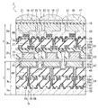
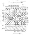
- FIG. 2 is a cross-sectional view of a main part showing the configuration of the semiconductor device according to the first embodiment of the present technology, and is a cross-sectional view of three pixels in FIG.
- the detailed configuration of the semiconductor device of the first embodiment will be described based on the cross-sectional view of the main part.
- the bonding surface 41 of the first substrate 2 and the bonding surface 71 of the second substrate 7 are arranged to face each other in a state where the metal thin film 12 is sandwiched between the first substrate 2 and the second substrate. It is an image sensor having a three-dimensional structure in which 7 and 7 are bonded together.
- the semiconductor layer 2a, the wiring layer 2b, and the electrode layer 2c are laminated in order from the side opposite to the second substrate 7, and the surface of the electrode layer 2c is relative to the second substrate 7. It is configured as a bonding surface 41.
- the semiconductor layer 7a, the wiring layer 7b, and the electrode layer 7c are laminated in order from the opposite side of the first substrate 2, and the surface of the electrode layer 7c is bonded to the first substrate 2. It is configured as a surface 71.
- a protective film 15, a color filter layer 17, and an on-chip lens 19 are laminated in the order shown on the surface of the first substrate 2 opposite to the second substrate 7.
- the detailed configurations of the layers constituting the first substrate 2 and the second substrate 7 and the metal thin film 12 will be sequentially described, and further, the configurations of the protective film 15, the color filter layer 17, and the on-chip lens 19 will be sequentially described. explain.
- the semiconductor layer 2a on the first substrate 2 side is a thin film of a semiconductor substrate 20 made of, for example, single crystal silicon.
- a photoelectric conversion unit 21 composed of an n-type impurity layer (or p-type impurity layer) is provided for each pixel. It is provided.
- a floating diffusion FD composed of an n + type impurity layer, a source / drain 23 of the transistor Tr, and another impurity layer (not shown here) are provided. ..
- the wiring layer 2b provided on the semiconductor layer 2a in the first substrate 2 has a transfer gate TG provided via a gate insulating film 25 on the interface side with the semiconductor layer 2a, a gate electrode 27 of the transistor Tr, and further. It has other electrodes (not shown here).
- the transfer gate TG and the gate electrode 27 are covered with an interlayer insulating film 29, and an embedded wiring 31 is provided in the groove pattern formed in the interlayer insulating film 29.
- the embedded wiring 31 is composed of a barrier metal layer 31a that covers the inner wall of the groove pattern, and a wiring layer 31b made of copper (Cu) embedded in the groove pattern via the barrier metal layer 31a.
- the wiring layer 2b as described above may be configured as a further laminated multi-layer wiring layer.
- the electrode layer 2c provided on the wiring layer 2b in the first substrate 2 has a diffusion-preventing insulating film 32 for copper (Cu) and a first insulating film 35 laminated on the interface side with the wiring layer 2b. It is equipped with.
- the first insulating film 35 is made of, for example, a TEOS film, and the first electrode 33 is provided as an embedded electrode in the groove pattern formed in the first insulating film 35.
- the TEOS film is a silicon oxide film formed by a chemical vapor deposition method (hereinafter referred to as CVD method) using TEOS gas (Tetra Ethoxy Silane gas: composition Si (OC2H5) 4) as a raw material gas. ..
- the first electrode 33 is composed of a barrier metal layer 33a that covers the inner wall of the groove pattern, and a first electrode film 33b made of copper (Cu) embedded in the groove pattern via the barrier metal layer 33a. ..
- the surface of the electrode layer 2c having such a configuration is the bonding surface 41 on the side of the first substrate 2 with respect to the second substrate 7.
- the bonded surface 41 is configured such that the first electrode 33 and the first insulating film 35 are exposed, and is in a state of being flattened by, for example, chemical mechanical polishing (hereinafter referred to as CMP).
- CMP chemical mechanical polishing
- a part of the groove pattern provided in the first insulating film 35 reaches the embedded wiring 31 provided in the wiring layer 2b and is embedded in the groove pattern.
- the first electrode 33 is connected to the embedded wiring 31 as needed.
- the semiconductor layer 7a on the second substrate 7 side is a thin film of a semiconductor substrate 50 made of, for example, single crystal silicon.
- the surface layer on the first substrate 2 side is provided with a source / drain 51 of the transistor Tr, an impurity layer (not shown here), and the like.
- the wiring layer 7b provided on the semiconductor layer 7a in the second substrate 7 has a gate electrode 55 provided on the interface side with the semiconductor layer 7a via a gate insulating film 53, and further, the illustration thereof is omitted here. It has other electrodes. These gate electrodes 55 and other electrodes are covered with an interlayer insulating film 57, and an embedded wiring 59 is provided in the groove pattern formed in the interlayer insulating film 57.
- the embedded wiring 59 is composed of a barrier metal layer 59a that covers the inner wall of the groove pattern, and a wiring layer 59b made of copper (Cu) embedded in the groove pattern via the barrier metal layer 59a.
- the wiring layer 7b as described above may have a multi-layer wiring layer structure.
- the electrode layer 7c provided on the wiring layer 7b in the second substrate 7 has a diffusion-preventing insulating film 61 against copper (Cu) on the interface side with the wiring layer 7b, and a second insulating film 69 laminated on the copper (Cu). And have.
- the second insulating film 69 is made of, for example, a TEOS film, and a second electrode 67 is provided as an embedded electrode in the groove pattern formed in the second insulating film 69.
- the second electrode 67 is composed of a barrier metal layer 67a that covers the inner wall of the groove pattern and a second electrode film 67b made of copper (Cu) embedded in the groove pattern via the barrier metal layer 67a.
- the second electrode 67 is arranged so as to correspond to the first electrode 33 on the first substrate 2 side, and is electrically connected to the first electrode 33 on the first substrate 2 side via the metal thin film 12. There is.
- the surface of such an electrode layer 7c is a bonding surface 71 on the side of the second substrate 7 with respect to the first substrate 2.
- the bonded surface 71 is configured such that the second electrode 67 and the second insulating film 69 are exposed, and is in a state of being flattened by, for example, CMP.
- the protective film 15 is provided so as to cover the photoelectric conversion unit 21 of the first substrate 2.
- the protective film 15 is made of a material film having passivation property, and for example, a silicon oxide film, a silicon nitride film, a silicon nitride film, or the like is used.
- the color filter layer 17 is composed of color filters of each color provided on a one-to-one basis corresponding to each photoelectric conversion unit 21.
- the arrangement of color filters for each color is not limited.
- the on-chip lens 19 is provided on a one-to-one basis corresponding to the color filters of each color constituting each photoelectric conversion unit 21 and the color filter layer 17, and is configured so that the incident light is focused on each photoelectric conversion unit 21. Has been done.
- Metal thin film 12 The metal thin film 12 is sandwiched between the bonding surface 41 on the first substrate 2 side and the bonding surface 71 on the second substrate 7 side, and covers the entire surface of the bonding surface 41 and the bonding surface 71. There is. That is, the first substrate 2 and the second substrate 7 are bonded to each other via the metal thin film 12.
- the digging portion 13 is provided between the adjacent first electrodes 33
- the digging portion 14 is provided between the adjacent second electrodes 67.
- the irradiated light passes through the on-chip lens 19 and the color filter layer 17, and the transmitted light is photoelectrically converted by the photoelectric conversion unit 21 to generate a signal charge. .. Then, the generated signal charge is passed through the transistor Tr formed in the wiring layer 2b to the first electrode 33 and the first electrode 33 as a pixel signal in the vertical signal line 6 shown in FIG. 1 formed by the embedded wiring 31. It is output to the second substrate 7 via the two electrodes 67.
- signal processing such as noise removal is performed for each pixel row for the signal output from the pixel 3 for one row.
- the second substrate 7 performs signal processing such as CDS (Correlated Double Sampling) and AD (Analog Digital) conversion for removing fixed pattern noise peculiar to pixels.
- FIG. 3 shows, as a comparative example, a step of bonding the bonding surface 41 on the first substrate 2 side and the bonding surface 71 on the second substrate 7 side.
- the surface of the second electrode 67 and the second insulating film 69 formed on the second substrate 7 is covered, and the metal thin film 12 is formed on the entire surface.
- the metal thin film 12 is formed of a material such as Ti, Ta, etc. to a thickness of 10 to 100 nm by using an ALD (Atomic Layer Deposition) method, a CVD (Chemical Vapor Deposition) method, or the like. After the metal thin film 12 is formed, the surface is flattened by using the CMP method or the like, if necessary.
- a first substrate 2 formed by the method shown in FIG. 3A is prepared, and a Wet using, for example, formic acid on the bonding surface 41 on the first substrate 2 side and the bonding surface 71 on the second substrate 7 side. Treatment or Dry treatment using plasma such as Ar, NH3, H2 is performed. By this treatment, the oxide film on the surface of the first electrode 33 and the surface of the second electrode 67 is removed to expose a clean metal surface. Then, as shown in FIG. 3B, the bonding surface 41 on the first substrate 2 side and the bonding surface 71 on the second substrate 7 side are opposed to each other, and both are bonded to each other.
- the joining technique when the joining technique is applied to a hybrid structure in which the first electrode 33 and the first insulating film 35 are present in the same plane, and a hybrid structure in which the second electrode 67 and the second insulating film 69 are present in the same plane, the first Silicon (Si) and metal deposited on the insulating film 35 and the second insulating film 69 serve as a leak source between the first electrode 33 and the second electrode 67, and are therefore shown in FIG. 3 (c) after joining.
- insulation by annealing (ANL) treatment is required.
- the ANL treatment is a treatment in which heat treatment is performed in an annealing device such as a hot plate or RTA in an N2 atmosphere or vacuum at atmospheric pressure, for example.
- the metal thin film 12 in the portion in contact with the first insulating film 35 and the second insulating film 69 reacts with each other.
- an insulating film 12a made of a reaction product is formed between the first substrate 2 and the second substrate 7.
- the ANL temperature is required to be 200 ° C or higher, and it is difficult to achieve a low temperature of 150 ° C or lower for the entire joining process.
- the hybrid bonding is performed by using atomic diffusion, and the structure has a recessed shape between the electrodes on the hybrid bonding surface.
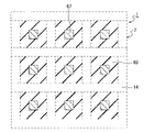
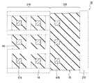
- FIG. 4 is a plan view of the second substrate 7 as viewed from the light incident side in the first embodiment.
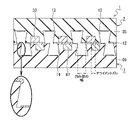
- FIG. 5 is a cross-sectional view showing a state in which the bonding surface 41 on the first substrate 2 side and the bonding surface 71 on the second substrate 7 side are bonded in the first embodiment.
- FIG. 4 illustrates a case where a plurality of second electrodes 67 are arranged at equal pitches in the row direction and the column direction.
- the plurality of second electrodes 67 are electrically separated by a digging portion 14 in which the second insulating film 69 is dug.
- the dug portion 14 is formed in a grid pattern so as to surround each of the second electrodes 67.
- the arrangement pattern of the second electrode 67 is not limited to the case of FIG. 4, and various arrangement patterns can be adopted.
- a digging portion 13 in which the first insulating film 35 is dug is formed between the adjacent first electrodes 33. Further, a digging portion 14 in which the second insulating film 69 is dug is formed between the adjacent second electrodes 67.
- the dug portions 13 and 14 divide the metal thin film 12. Further, the dug portions 13 and 14 have a reverse taper shape, and the metal thin film 12 is divided in the middle.
- the dug portions 13 and 14 can also absorb the misalignment between the first electrode 33 and the second electrode 67.
- the opening width of each of the dug portions 13 and 14 is larger than twice the alignment deviation that occurs when the first electrode 33 and the second electrode 67 are joined.
- the opening width is the opening width on the side of the bonding surface 41 on the side of the first substrate 2 and the side of the bonding surface 71 on the side of the second substrate 7.
- the metal thin film 12 between the first electrodes 33 is separated by the dug portion 13, and the metal thin film 12 between the second electrodes 67 is separated by the dug portion 14. This makes it possible to reduce the temperature of the entire joining process to room temperature. Further, the capacity can be expected to be reduced by providing the gap structure on the bonding surface 41 on the first substrate 2 side and the bonding surface 71 on the second substrate 7 side.
- the dug portions 13 and 14 by forming the dug portions 13 and 14 into a reverse taper shape, a vacuum having a large volume can be created, whereby the temperature of the entire joining process can be lowered to room temperature. Become. Further, according to the first embodiment, when the alignment deviation generated at the time of joining the first electrode 33 and the second electrode 67 can be predicted to some extent, the opening widths of the dug portions 13 and 14 are set to the alignment deviation 2. If it is made larger than twice, the misalignment can be absorbed.
- FIG. 6 is a cross-sectional view of a main part showing a configuration of a semiconductor device as a first modification of the first embodiment of the present technology.
- the same parts as those in FIG. 2 are designated by the same reference numerals, and detailed description thereof will be omitted.
- the insulating film 22 is formed in a region other than the color filter layer 17.
- One pixel 3 is formed for each set of the color filter layer 17, the on-chip lens 19, and the photoelectric conversion unit 21.
- the first insulating film 35 is made of, for example, a TEOS film, and a first electrode pad 331 and a dummy electrode 332 are provided as embedded electrodes in the groove pattern formed in the first insulating film 35. There is.
- the second insulating film 69 is made of, for example, a TEOS film, and a second electrode pad 671 and a dummy electrode 672 are provided as embedded electrodes in the groove pattern formed in the second insulating film 69. There is.
- the digging portion where the first insulating film 35 is dug between the adjacent first electrode pad 331 and the dummy electrode 332 and between the adjacent dummy electrodes 332. 13 is formed. Further, a digging portion 14 in which the second insulating film 69 is dug is formed between the adjacent second electrode pad 671 and the dummy electrode 672, and between the adjacent dummy electrodes 672.
- the dug portions 13 and 14 have a reverse taper shape, and the metal thin film 12 is divided in the middle.
- FIG. 7 is a cross-sectional view of a main part showing a configuration of a semiconductor device as a second modification of the first embodiment of the present technology.
- the same parts as those in FIG. 2 are designated by the same reference numerals, and detailed description thereof will be omitted.
- the first substrate 2 is a first semiconductor substrate 33-1 made of thinned silicon, in which a photodiode PD serving as a photoelectric conversion unit and a plurality of pixels composed of a plurality of pixel transistors Tr1 and Tr2 are arranged in a row.
- a pixel array 34 arranged two-dimensionally in a shape is formed.
- a plurality of MOS transistors constituting a control circuit are formed on the first semiconductor substrate 33-1.
- a plurality of wires 351-1 to 354-1 and wiring 333 made of four layers of metals M1 to M4 are provided via the first insulating film 35 in this example.
- the arranged multilayer wiring layer 37-1 is formed.
- copper (Cu) wirings formed by the dual damascene method are used.
- a light-shielding film 39-1 including the optical black region 41-1 is formed on the back surface side of the first semiconductor substrate 33-1 via an insulating film 38-1, and further via a flattening film 43-1.
- the color filter 44-1 and the on-semiconductor substrate lens 45-1 are formed on the effective pixel array 42-1.
- the on-semiconductor substrate lens 45-1 can also be formed on the optical black region 41-1.
- the conductive via 52 is located between the corresponding pixel transistor and the wiring 351-1 to 354-1 and between the adjacent upper and lower layer wirings 351-1 to 354-1 and the wiring 333. Connected via -1. Further, the wiring 333 is connected to the required wiring 354-1 by the metal M3 of the third layer via the conductive via 52-1. Further, a vertical signal line 6 is formed on the third layer.
- a logic circuit 55-1 constituting a peripheral circuit is formed in a region of each semiconductor substrate of the second semiconductor substrate 54-1 made of silicon.
- the logic circuit 55-1 is formed by a plurality of MOS transistors Tr11 to Tr14 including CMOS transistors.
- Wiring 571-1 to 574-1 and wiring 673 made of metal M11 to M14 having a plurality of layers, in this example, four layers are arranged on the surface side of the second semiconductor substrate 54-1 via the second insulating film 69.
- the multi-layer wiring layer 59-1 is formed. Copper (Cu) wiring by the dual damascene method is used for wirings 571-1 to 574-1 and wiring 673.
- the conductive via 64 is located between the MOS transistors Tr11 to Tr14 and the wirings 571-1 to 573-1 and between the adjacent upper and lower layer wirings 571-1 to 573-1. It is connected via -1. Further, a wiring 673 made of the fourth metal M14 is formed so as to face the joint surface with the first substrate 2. The wiring 673 is connected to the required wiring 5731 by the third metal M13 via the conductive via 64-1.
- the first substrate 2 and the second substrate 7 are bonded to each other via a metal thin film 12.
- the digging portion 13 in which the first insulating film 35 is dug is formed between the wiring 333 and the wiring 334 and between the adjacent wirings 334.
- a digging portion 14 in which the second insulating film 69 is dug is formed between the wiring 673 and the wiring 674, and between the adjacent wirings 674.
- the dug portions 13 and 14 have a reverse taper shape, and the metal thin film 12 is divided in the middle.
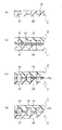
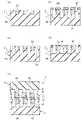
- FIG. 8 shows a process flow for forming the semiconductor device 1 according to the second embodiment of the present technology.
- the surfaces of the second electrode 67 and the second insulating film 69 formed on the second substrate 7 are flattened by a CMP method or the like as necessary to perform a hybrid. Form the structure.
- a resist pattern 100 is formed on the surfaces of the second electrode 67 and the second insulating film 69 by using lithography, and DRY is formed with respect to the second insulating film 69.
- An etching process is performed to form a dug portion 14 between the second electrodes 67.
- the reverse taper shape enables more reliable separation between the second electrodes 67 at the time of metal film sputtering of atomic diffusion bonding.
- resist stripping is performed to remove the resist pattern 100.
- CMP may be performed again to clean the bonded surface, that is, the bonded surface 71.
- metal sputtering is performed in the atomic diffusion bonding device to form the metal thin film 12 on the surface of the second electrode 67.
- the first substrate 2 formed by the methods shown in FIGS. 8 (a) to 8 (d) is prepared, and the bonding surface 41 and the first substrate 2 on the first substrate 2 side are prepared. 2 Align with the bonding surface 71 on the 7 side of the substrate and join them together.
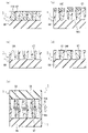
- FIG. 9 shows a process flow for forming the semiconductor device 1 according to the third embodiment of the present technology.
- the surfaces of the second electrode 67 and the second insulating film 69 formed on the second substrate 7 are flattened by a CMP method or the like as necessary to perform a hybrid.
- the reverse taper dummy pattern 110 is formed.
- a resist pattern 100 is formed on the surfaces of the second electrode 67, the second insulating film 69, and the reverse taper dummy pattern 110 by using lithography, and the reverse taper dummy is formed.
- the pattern 110 is subjected to WET etching treatment to remove the Cu electrode of the reverse taper dummy pattern 110, and a dug portion 14A is formed between the second electrodes 67.
- resist stripping is performed to remove the resist pattern 100.
- CMP may be performed again to clean the bonded surface, that is, the bonded surface 71.
- metal sputtering is performed in the atomic diffusion bonding device to form the metal thin film 12 on the surface of the second electrode 67.
- FIG. 9 (e) the first substrate 2 formed by the methods shown in FIGS. 9 (a) to 9 (d) is prepared, and the bonding surface 41 and the first substrate 2 on the first substrate 2 side are prepared. 2 Align with the bonding surface 71 on the 7 side of the substrate and join them together.
- the third embodiment by forming the reverse taper dummy pattern 110, the depth between the first electrode 33 and the digging portion 13, the second electrode 67 and the digging portion 14 The depths of the digging portions 13 and 14 can be made uniform, and the formation regions of the dug portions 13 and 14 can be made smaller, which contributes to the miniaturization of the semiconductor device 1.
- FIG. 10 is a plan view of the second substrate 7A as viewed from the light incident side as the fourth embodiment of the present technique.
- the same parts as those in FIG. 4 are designated by the same reference numerals, and detailed description thereof will be omitted.
- a plurality of second electrodes 67 are arranged at equal pitches in the row direction and the column direction.
- the plurality of second electrodes 67 are electrically separated by the dug portion 14B into which the second insulating film 69 of the second substrate 7A is dug.
- the dug portion 14B is formed in a ring shape so as to surround each of the second electrodes 67, and the second electrode 67 is located at the center of the ring shape.
- the dug portion 14B has a square shape, but it may be circular. Further, although not shown in FIG. 10, a plurality of first electrodes 33 are arranged at equal pitches in the row direction and the column direction on the first substrate 2, and a ring is formed around each first electrode 33. It is surrounded by a shaped digging portion 13. Then, the second substrate 7A is aligned with the first substrate 2 and joined to the first substrate 2. As a result, the semiconductor device 1C is formed.
- the fourth embodiment by forming the ring-shaped digging portion 14B around each of the plurality of second electrodes 67, the temperature of the entire joining process is further higher than that of the first embodiment. Can be cooled to room temperature.
- FIG. 11 is a plan view of the second substrate 7B as viewed from the light incident side as the fifth embodiment of the present technique.
- the same parts as those in FIG. 4 are designated by the same reference numerals, and detailed description thereof will be omitted.
- the second substrate 7B is divided into a region 210 that requires separation between electrodes, a region 220 that does not require separation, and a dicing region 230.
- a plurality of second electrodes 67A are arranged at equal pitches in the row direction and the column direction.
- the plurality of second electrodes 67A are electrically separated by a digging portion 14 in which the second insulating film 69 of the second substrate 7A is dug.
- a plurality of second electrodes 67B are arranged at equal pitches in the column direction.
- the plurality of second electrodes 67B may be arranged at equal pitches in the row direction. Since the dicing region 230 needs to be strong, it is desirable not to provide the dug portion 14.
- the first substrate 2 is also divided into a region 210 that requires separation between electrodes, a region 220 that does not require separation, and a dicing region 230. Then, the second substrate 7B is aligned with the first substrate 2 and joined to the first substrate 2. As a result, the semiconductor device 1D is formed.
- the temperature of the entire joining process is controlled by dividing the second substrate 7B into a region 210 that requires separation between electrodes, a region 220 that does not require separation, and a dicing region 230.
- the temperature can be lowered to room temperature, and the bonding strength of the semiconductor device 1D can be improved.
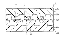
- FIG. 12 is a cross-sectional view showing a state in which the first substrate 2C and the second substrate 7C are bonded together as the sixth embodiment of the present technology.
- the same parts as those in FIG. 5 are designated by the same reference numerals, and detailed description thereof will be omitted.
- Inorganic insulating films such as SiO2, SiN, SiCN, and SiCO are used for the first insulating film 35A and the second insulating film 69A.
- an organic insulating film containing polyimide or the like may be used, or a metal oxide such as Al2O3 or TiO2 may be used.
- the metal thin film 12A a metal capable of sputtering such as Ti, Cr, Mn, Au, and Al is used.
- a conductive oxide such as ITO or IZGO may be used for the metal thin film 12A.
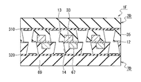
- FIG. 13 is a cross-sectional view showing a state in which the first substrate 2D and the second substrate 7D are bonded together as the seventh embodiment of the present technology.
- the same parts as those in FIG. 5 are designated by the same reference numerals, and detailed description thereof will be omitted.
- an etching stopper layer 310 for aligning the bottom surface of the dug portion 13 is formed on the first insulating film 35 of the first substrate 2D. Further, an etching stopper layer 320 for aligning the bottom surface of the dug portion 14 is formed on the second insulating film 69 of the second substrate 7D.
- a film type different from the first insulating film 35 and the second insulating film 69 such as SiN, SiCN, and SiCO is used.
- the second substrate 7D is aligned with the first substrate 2D and joined to the first substrate 2D.
- the semiconductor device 1F is formed.
- the etching stopper layer 310 for aligning the bottom surface of the dug portion 13 is formed on the first insulating film 35 of the first substrate 2D, and the second substrate 7D is second.
- the etching stopper layer 320 for aligning the bottom surfaces of the digging portions 14 is formed on the insulating film 69, it is useful for controlling the shape of the openings of the plurality of digging portions 13 and the plurality of digging portions 14.
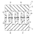
- FIG. 14 is a cross-sectional view showing a state in which the first substrate 2E and the second substrate 7E are bonded together as the eighth embodiment of the present technology.
- the same parts as those in FIG. 5 are designated by the same reference numerals, and detailed description thereof will be omitted.
- a digging portion 410 in which the first insulating film 35 is dug is formed between the adjacent first electrodes 33. Further, a digging portion 420 in which the second insulating film 69 is dug is formed between the adjacent second electrodes 67.
- the digging portion 410 is located on the bottom surface side of the first opening 411 having a diameter R1 from the bonding surface side of the first substrate 2E side toward the bottom surface side and the first opening 411, and from the diameter R1. It is composed of a second opening 412 having a large diameter R2.
- the dug portion 420 is located on the bottom surface side of the first opening 421 having a diameter R1 from the bonding surface side of the second substrate 7E side toward the bottom surface side, and from the diameter R1. It is composed of a second opening 422 having a large diameter R2.
- the second substrate 7E is aligned with the first substrate 2E and joined to the first substrate 2E.
- the semiconductor device 1G is formed.
- the digging portion 410 has a two-stage configuration of the first opening 411 and the second opening 412, and the digging portion 420 has the first opening 421.
- the two-stage structure By forming the two-stage structure with the second opening 422, it is possible to more reliably divide the metal thin film 12 at the time of metal sputtering of the atomic diffusion bond.
- FIG. 15 is a cross-sectional view showing a state in which the first substrate 2 and the second substrate 7 are bonded together as another embodiment of the present technology.
- the same parts as those in FIG. 5 are designated by the same reference numerals, and detailed description thereof will be omitted.
- the metal thin film 12B is composed of a first metal thin film 121 formed on the bonding surface 41 on the first substrate 2 side and a second metal thin film 122 formed on the bonding surface 71 on the second substrate 7 side. .. Then, the second substrate 7 is aligned with the first substrate 2 and is joined to the first substrate 2 while the first metal thin film 121 and the second metal thin film 122 are separated. As a result, the semiconductor device 1H is formed.
- the bonding interface between the first metal thin film 121 and the second metal thin film 122 after bonding may or may not be flat. Further, between the dug portion 13 and the dug portion 14, one end of the first metal thin film 121 and one end of the second metal thin film 122 may be joined so as to be offset or aligned.
- FIG. 16 as another embodiment of the present technique, one end of the first metal thin film 121 and one end of the second metal thin film 122 are aligned between the dug portion 13 and the dug portion 14, and the first substrate is shown. It is sectional drawing which shows the state which 2 and the 2nd substrate 7 are bonded together. In FIG. 16, the same parts as those in FIG. 15 are designated by the same reference numerals, and detailed description thereof will be omitted.
- the second substrate 7 is aligned with the first substrate 2, and one end of the first metal thin film 121 and one end of the second metal thin film 122 are aligned between the dug portion 13 and the dug portion 14, and the second substrate 7 is the second.
- the 1 metal thin film 121 and the 2nd metal thin film 122 are joined to the 1st substrate 2 while being separated. As a result, the semiconductor device 1I is formed.
- the metal thin film 12B may be configured such that the first metal thin film 121 and the second metal thin film 122 are bonded as they are, or may be integrated after bonding. Further, examples of the first metal thin film 121 and the second metal thin film 122 being joined while being separated are the first modification and the second modification of the first to eighth embodiments and the first embodiment. It can also be applied to the configuration of the metal thin film 12 in the example.
- the first electrode 33 is embedded in the first insulating film 35 and the second electrode 67 is embedded in the second insulating film 69
- the first insulating film 35 may form a plurality of insulating films laminated in multiple layers
- the second insulating film 69 may form a plurality of insulating films laminated in multiple layers. good.
- the first electrode 33 may be formed so as to be embedded across a plurality of insulating films.
- the second electrode 67 may be formed so as to be embedded across a plurality of insulating films.
- the first electrode 33 and the second electrode 67 may be formed outside the pixel region.
- a set of the first electrode 33 and the second electrode 67 may be electrically connected to a plurality of pixels in the pixel region or outside the pixel region.
- the power supplied from the outside to the first substrate 2 can be supplied to the second substrate 7 via the first electrode 33 and the second electrode 67. Further, it can be connected to a reference potential (ground potential or fixed potential) via the first electrode 33 and the second electrode 67 so as to realize an electrical shield.
- the technique according to the present disclosure can be applied to various products.
- the techniques according to the present disclosure may be applied to an endoscopic surgery system.
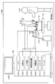
- FIG. 17 is a diagram showing an example of a schematic configuration of an endoscopic surgery system to which the technique according to the present disclosure (the present technique) can be applied.
- FIG. 17 shows a surgeon (doctor) 11131 performing surgery on patient 11132 on patient bed 11133 using the endoscopic surgery system 11000.
- the endoscopic surgery system 11000 includes an endoscope 11100, other surgical tools 11110 such as an abdominal tube 11111 and an energy treatment tool 11112, and a support arm device 11120 that supports the endoscope 11100.
- a cart 11200 equipped with various devices for endoscopic surgery.
- the endoscope 11100 is composed of a lens barrel 11101 in which a region having a predetermined length from the tip is inserted into the body cavity of the patient 11132, and a camera head 11102 connected to the base end of the lens barrel 11101.
- the endoscope 11100 configured as a so-called rigid mirror having a rigid barrel 11101 is illustrated, but the endoscope 11100 may be configured as a so-called flexible mirror having a flexible barrel. good.
- An opening in which an objective lens is fitted is provided at the tip of the lens barrel 11101.
- a light source device 11203 is connected to the endoscope 11100, and the light generated by the light source device 11203 is guided to the tip of the lens barrel by a light guide extending inside the lens barrel 11101, and is an objective. It is irradiated toward the observation target in the body cavity of the patient 11132 through the lens.
- the endoscope 11100 may be a direct endoscope, a perspective mirror, or a side endoscope.
- An optical system and an image sensor are provided inside the camera head 11102, and the reflected light (observation light) from the observation target is focused on the image sensor by the optical system.
- the observation light is photoelectrically converted by the image pickup device, and an electric signal corresponding to the observation light, that is, an image signal corresponding to the observation image is generated.
- the image signal is transmitted as RAW data to the camera control unit (CCU: Camera Control Unit) 11201.
- CCU Camera Control Unit
- the CCU11201 is composed of a CPU (Central Processing Unit), a GPU (Graphics Processing Unit), and the like, and comprehensively controls the operations of the endoscope 11100 and the display device 11202. Further, the CCU11201 receives an image signal from the camera head 11102, and performs various image processing on the image signal for displaying an image based on the image signal, such as development processing (demosaic processing). The display device 11202 displays an image based on the image signal processed by the CCU 11201 under the control of the CCU 11201.
- a CPU Central Processing Unit
- GPU Graphics Processing Unit
- the light source device 11203 is composed of, for example, a light source such as an LED (Light Emitting Diode), and supplies irradiation light for photographing an operating part or the like to the endoscope 11100.
- the input device 11204 is an input interface to the endoscopic surgery system 11000.
- the user can input various information and input instructions to the endoscopic surgery system 11000 via the input device 11204. For example, the user inputs an instruction to change the imaging conditions (type of irradiation light, magnification, focal length, etc.) by the endoscope 11100.
- the treatment tool control device 11205 controls the drive of the energy treatment tool 11112 for cauterizing, incising, sealing a blood vessel, or the like.
- the pneumoperitoneum device 11206 uses a gas in the pneumoperitoneum tube 11111 to inflate the body cavity of the patient 11132 for the purpose of securing the field of view by the endoscope 11100 and securing the work space of the operator. Is sent.
- the recorder 11207 is a device capable of recording various information related to surgery.
- the printer 11208 is a device capable of printing various information related to surgery in various formats such as text, images, and graphs.
- the light source device 11203 that supplies the irradiation light to the endoscope 11100 when photographing the surgical site can be composed of, for example, an LED, a laser light source, or a white light source composed of a combination thereof.
- a white light source is configured by a combination of RGB laser light sources, the output intensity and output timing of each color (each wavelength) can be controlled with high accuracy. Therefore, the light source device 11203 adjusts the white balance of the captured image. It can be carried out.
- the laser light from each of the RGB laser light sources is irradiated to the observation target in a time-division manner, and the drive of the image sensor of the camera head 11102 is controlled in synchronization with the irradiation timing to correspond to each of RGB. It is also possible to capture the image in a time-division manner. According to this method, a color image can be obtained without providing a color filter in the image pickup device.
- the drive of the light source device 11203 may be controlled so as to change the intensity of the output light at predetermined time intervals.
- the drive of the image sensor of the camera head 11102 in synchronization with the timing of the change of the light intensity to acquire an image in time division and synthesizing the image, so-called high dynamic without blackout and overexposure. Range images can be generated.
- the light source device 11203 may be configured to be able to supply light in a predetermined wavelength band corresponding to special light observation.
- special light observation for example, by utilizing the wavelength dependence of light absorption in body tissue to irradiate light in a narrower band than the irradiation light (that is, white light) during normal observation, the surface layer of the mucous membrane.
- a so-called narrow band imaging is performed in which a predetermined tissue such as a blood vessel is photographed with high contrast.
- fluorescence observation may be performed in which an image is obtained by fluorescence generated by irradiating with excitation light.
- the body tissue is irradiated with excitation light to observe the fluorescence from the body tissue (autofluorescence observation), or a reagent such as indocyanine green (ICG) is locally injected into the body tissue and the body tissue is injected. It is possible to obtain a fluorescence image by irradiating the excitation light corresponding to the fluorescence wavelength of the reagent.
- the light source device 11203 may be configured to be capable of supplying narrowband light and / or excitation light corresponding to such special light observation.
- FIG. 18 is a block diagram showing an example of the functional configuration of the camera head 11102 and CCU11201 shown in FIG.
- the camera head 11102 includes a lens unit 11401, an image pickup unit 11402, a drive unit 11403, a communication unit 11404, and a camera head control unit 11405.
- CCU11201 has a communication unit 11411, an image processing unit 11412, and a control unit 11413.
- the camera head 11102 and CCU11201 are communicably connected to each other by a transmission cable 11400.
- the lens unit 11401 is an optical system provided at a connection portion with the lens barrel 11101.
- the observation light taken in from the tip of the lens barrel 11101 is guided to the camera head 11102 and incident on the lens unit 11401.
- the lens unit 11401 is configured by combining a plurality of lenses including a zoom lens and a focus lens.
- the image pickup unit 11402 is composed of an image pickup element.
- the image pickup element constituting the image pickup unit 11402 may be one (so-called single plate type) or a plurality (so-called multi-plate type).
- each image pickup element may generate an image signal corresponding to each of RGB, and a color image may be obtained by synthesizing them.
- the image pickup unit 11402 may be configured to have a pair of image pickup elements for acquiring image signals for the right eye and the left eye corresponding to 3D (Dimensional) display, respectively.
- the 3D display enables the operator 11131 to more accurately grasp the depth of the living tissue in the surgical site.
- a plurality of lens units 11401 may be provided corresponding to each image pickup element.
- the image pickup unit 11402 does not necessarily have to be provided on the camera head 11102.
- the image pickup unit 11402 may be provided inside the lens barrel 11101 immediately after the objective lens.
- the drive unit 11403 is composed of an actuator, and is controlled by the camera head control unit 11405 to move the zoom lens and the focus lens of the lens unit 11401 by a predetermined distance along the optical axis. As a result, the magnification and focus of the image captured by the image pickup unit 11402 can be adjusted as appropriate.
- the communication unit 11404 is configured by a communication device for transmitting and receiving various information to and from the CCU11201.
- the communication unit 11404 transmits the image signal obtained from the image pickup unit 11402 as RAW data to the CCU 11201 via the transmission cable 11400.
- the communication unit 11404 receives a control signal for controlling the drive of the camera head 11102 from the CCU 11201 and supplies the control signal to the camera head control unit 11405.
- the control signal includes, for example, information to specify the frame rate of the captured image, information to specify the exposure value at the time of imaging, and / or information to specify the magnification and focus of the captured image. Contains information about the condition.
- the image pickup conditions such as the frame rate, exposure value, magnification, and focus may be appropriately specified by the user, or may be automatically set by the control unit 11413 of the CCU11201 based on the acquired image signal. good.
- the endoscope 11100 is equipped with a so-called AE (Auto Exposure) function, an AF (Auto Focus) function, and an AWB (Auto White Balance) function.
- the camera head control unit 11405 controls the drive of the camera head 11102 based on the control signal from the CCU 11201 received via the communication unit 11404.
- the communication unit 11411 is configured by a communication device for transmitting and receiving various information to and from the camera head 11102.
- the communication unit 11411 receives an image signal transmitted from the camera head 11102 via the transmission cable 11400.
- the communication unit 11411 transmits a control signal for controlling the drive of the camera head 11102 to the camera head 11102.
- Image signals and control signals can be transmitted by telecommunications, optical communication, or the like.
- the image processing unit 11412 performs various image processing on the image signal which is the RAW data transmitted from the camera head 11102.
- the control unit 11413 performs various controls related to the imaging of the surgical site and the like by the endoscope 11100 and the display of the captured image obtained by the imaging of the surgical site and the like. For example, the control unit 11413 generates a control signal for controlling the drive of the camera head 11102.
- control unit 11413 causes the display device 11202 to display an image captured by the surgical unit or the like based on the image signal processed by the image processing unit 11412.
- the control unit 11413 may recognize various objects in the captured image by using various image recognition techniques.
- the control unit 11413 detects a surgical tool such as forceps, a specific biological part, bleeding, mist when using the energy treatment tool 11112, etc. by detecting the shape, color, etc. of the edge of the object included in the captured image. Can be recognized.
- the control unit 11413 may superimpose and display various surgical support information on the image of the surgical unit by using the recognition result. By superimposing and displaying the surgical support information and presenting it to the surgeon 11131, the burden on the surgeon 11131 can be reduced and the surgeon 11131 can surely proceed with the surgery.
- the transmission cable 11400 connecting the camera head 11102 and CCU11201 is an electric signal cable corresponding to electric signal communication, an optical fiber corresponding to optical communication, or a composite cable thereof.
- the communication is performed by wire using the transmission cable 11400, but the communication between the camera head 11102 and the CCU11201 may be performed wirelessly.
- the above is an example of an endoscopic surgery system to which the technique according to the present disclosure can be applied.
- the technique according to the present disclosure can be applied to, for example, the endoscope 11100, the image pickup unit 11402 of the camera head 11102, the image processing unit 11412 of the CCU 11201, and the like among the configurations described above.
- the semiconductor device 1 of FIG. 1 can be applied to the image pickup unit 10402.
- the technique according to the present disclosure may be applied to other, for example, a microscopic surgery system.
- the technique according to the present disclosure can be applied to various products.
- the technology according to the present disclosure is realized as a device mounted on a moving body of any kind such as an automobile, an electric vehicle, a hybrid electric vehicle, a motorcycle, a bicycle, a personal mobility, an airplane, a drone, a ship, and a robot. You may.
- FIG. 19 is a block diagram showing a schematic configuration example of a vehicle control system, which is an example of a mobile control system to which the technique according to the present disclosure can be applied.
- the vehicle control system 12000 includes a plurality of electronic control units connected via the communication network 12001.
- the vehicle control system 12000 includes a drive system control unit 12010, a body system control unit 12020, an outside information detection unit 12030, an in-vehicle information detection unit 12040, and an integrated control unit 12050.
- a microcomputer 12051, an audio image output unit 12052, and an in-vehicle network I / F (interface) 12053 are shown.
- the drive system control unit 12010 controls the operation of the device related to the drive system of the vehicle according to various programs.
- the drive system control unit 12010 has a driving force generator for generating a driving force of a vehicle such as an internal combustion engine or a driving motor, a driving force transmission mechanism for transmitting the driving force to the wheels, and a steering angle of the vehicle. It functions as a control device such as a steering mechanism for adjusting and a braking device for generating braking force of the vehicle.
- the body system control unit 12020 controls the operation of various devices mounted on the vehicle body according to various programs.
- the body system control unit 12020 functions as a keyless entry system, a smart key system, a power window device, or a control device for various lamps such as headlamps, back lamps, brake lamps, turn signals or fog lamps.
- the body system control unit 12020 may be input with radio waves transmitted from a portable device that substitutes for the key or signals of various switches.
- the body system control unit 12020 receives inputs of these radio waves or signals and controls a vehicle door lock device, a power window device, a lamp, and the like.
- the outside information detection unit 12030 detects information outside the vehicle equipped with the vehicle control system 12000.
- the image pickup unit 12031 is connected to the vehicle outside information detection unit 12030.
- the vehicle outside information detection unit 12030 causes the image pickup unit 12031 to capture an image of the outside of the vehicle and receives the captured image.
- the out-of-vehicle information detection unit 12030 may perform object detection processing or distance detection processing such as a person, a vehicle, an obstacle, a sign, or a character on the road surface based on the received image.
- the image pickup unit 12031 is an optical sensor that receives light and outputs an electric signal according to the amount of the light received.
- the image pickup unit 12031 can output an electric signal as an image or can output it as distance measurement information. Further, the light received by the image pickup unit 12031 may be visible light or invisible light such as infrared light.
- the in-vehicle information detection unit 12040 detects the in-vehicle information.
- a driver state detection unit 12041 that detects a driver's state is connected to the vehicle interior information detection unit 12040.
- the driver state detection unit 12041 includes, for example, a camera that images the driver, and the in-vehicle information detection unit 12040 determines the degree of fatigue or concentration of the driver based on the detection information input from the driver state detection unit 12041. It may be calculated, or it may be determined whether or not the driver has fallen asleep.
- the microcomputer 12051 calculates the control target value of the driving force generator, the steering mechanism, or the braking device based on the information inside and outside the vehicle acquired by the vehicle exterior information detection unit 12030 or the vehicle interior information detection unit 12040, and the drive system control unit.
- a control command can be output to 12010.
- the microcomputer 12051 realizes ADAS (Advanced Driver Assistance System) functions including vehicle collision avoidance or impact mitigation, follow-up driving based on inter-vehicle distance, vehicle speed maintenance driving, vehicle collision warning, vehicle lane deviation warning, and the like. It is possible to perform cooperative control for the purpose of.
- ADAS Advanced Driver Assistance System
- the microcomputer 12051 controls the driving force generating device, the steering mechanism, the braking device, and the like based on the information around the vehicle acquired by the outside information detection unit 12030 or the inside information detection unit 12040, so that the driver can control the driver. It is possible to perform coordinated control for the purpose of automatic driving that runs autonomously without depending on the operation.
- the microcomputer 12051 can output a control command to the body system control unit 12020 based on the information outside the vehicle acquired by the vehicle outside information detection unit 12030.
- the microcomputer 12051 controls the headlamps according to the position of the preceding vehicle or the oncoming vehicle detected by the outside information detection unit 12030, and performs cooperative control for the purpose of anti-glare such as switching the high beam to the low beam. It can be carried out.
- the audio image output unit 12052 transmits an output signal of at least one of audio and image to an output device capable of visually or audibly notifying information to the passenger or the outside of the vehicle.
- an audio speaker 12061, a display unit 12062, and an instrument panel 12063 are exemplified as output devices.
- the display unit 12062 may include, for example, at least one of an onboard display and a head-up display.
- FIG. 20 is a diagram showing an example of the installation position of the image pickup unit 12031.
- the vehicle 12100 has image pickup units 12101, 12102, 12103, 12104, 12105 as image pickup units 12031.
- the image pickup units 12101, 12102, 12103, 12104, 12105 are provided, for example, at positions such as the front nose, side mirrors, rear bumpers, back doors, and the upper part of the windshield in the vehicle interior of the vehicle 12100.
- the image pickup unit 12101 provided in the front nose and the image pickup section 12105 provided in the upper part of the windshield in the vehicle interior mainly acquire an image in front of the vehicle 12100.
- the image pickup units 12102 and 12103 provided in the side mirror mainly acquire images of the side of the vehicle 12100.
- the image pickup unit 12104 provided in the rear bumper or the back door mainly acquires an image of the rear of the vehicle 12100.
- the images in front acquired by the image pickup units 12101 and 12105 are mainly used for detecting a preceding vehicle, a pedestrian, an obstacle, a traffic light, a traffic sign, a lane, or the like.
- FIG. 20 shows an example of the shooting range of the imaging units 12101 to 12104.
- the imaging range 12111 indicates the imaging range of the imaging unit 12101 provided on the front nose
- the imaging ranges 12112 and 12113 indicate the imaging range of the imaging units 12102 and 12103 provided on the side mirrors, respectively
- the imaging range 12114 indicates the imaging range.
- the imaging range of the imaging unit 12104 provided on the rear bumper or the back door is shown. For example, by superimposing the image data captured by the imaging units 12101 to 12104, a bird's-eye view image of the vehicle 12100 can be obtained.
- At least one of the image pickup units 12101 to 12104 may have a function of acquiring distance information.
- at least one of the image pickup units 12101 to 12104 may be a stereo camera including a plurality of image pickup elements, or may be an image pickup element having pixels for phase difference detection.
- the microcomputer 12051 has a distance to each three-dimensional object within the image pickup range 12111 to 12114 based on the distance information obtained from the image pickup unit 12101 to 12104, and a temporal change of this distance (relative speed with respect to the vehicle 12100). By obtaining can. Further, the microcomputer 12051 can set an inter-vehicle distance to be secured in advance in front of the preceding vehicle, and can perform automatic braking control (including follow-up stop control), automatic acceleration control (including follow-up start control), and the like. In this way, it is possible to perform coordinated control for the purpose of automatic driving or the like that autonomously travels without relying on the driver's operation.
- automatic braking control including follow-up stop control
- automatic acceleration control including follow-up start control
- the microcomputer 12051 converts three-dimensional object data related to a three-dimensional object into two-wheeled vehicles, ordinary vehicles, large vehicles, pedestrians, electric poles, and other three-dimensional objects based on the distance information obtained from the image pickup units 12101 to 12104. It can be classified and extracted and used for automatic avoidance of obstacles. For example, the microcomputer 12051 distinguishes obstacles around the vehicle 12100 into obstacles that are visible to the driver of the vehicle 12100 and obstacles that are difficult to see. Then, the microcomputer 12051 determines the collision risk indicating the risk of collision with each obstacle, and when the collision risk is equal to or higher than the set value and there is a possibility of collision, the microcomputer 12051 via the audio speaker 12061 or the display unit 12062. By outputting an alarm to the driver and performing forced deceleration and avoidance steering via the drive system control unit 12010, driving support for collision avoidance can be provided.
- At least one of the image pickup units 12101 to 12104 may be an infrared camera that detects infrared rays.
- the microcomputer 12051 can recognize a pedestrian by determining whether or not a pedestrian is present in the captured image of the imaging unit 12101 to 12104.
- recognition of a pedestrian is, for example, a procedure for extracting feature points in an image captured by an image pickup unit 12101 to 12104 as an infrared camera, and pattern matching processing is performed on a series of feature points indicating the outline of an object to determine whether or not the pedestrian is a pedestrian. It is done by the procedure to determine.
- the audio image output unit 12052 determines the square contour line for emphasizing the recognized pedestrian.
- the display unit 12062 is controlled so as to superimpose and display. Further, the audio image output unit 12052 may control the display unit 12062 so as to display an icon or the like indicating a pedestrian at a desired position.
- the above is an example of a vehicle control system to which the technique according to the present disclosure can be applied.
- the technique according to the present disclosure can be applied to, for example, the image pickup unit 12031 among the configurations described above.
- the semiconductor device 1 of FIG. 1 can be applied to the image pickup unit 12031.
- the present disclosure may also have the following structure. (1) The first insulating film formed on the first semiconductor substrate and A plurality of first junction electrodes formed on the surface of the first insulating film, and A second insulating film formed on the second semiconductor substrate that is hybrid-bonded to the first semiconductor substrate, A plurality of second junction electrodes formed on the surface of the second insulating film, and A metal film covering the entire surface of the bonding surface composed of the first insulating film and the plurality of first bonding electrodes, and the entire surface of the bonding surface composed of the second insulating film and the plurality of second bonding electrodes.
- the first insulating film is formed between at least a part of the bonding electrodes of the plurality of first bonding electrodes, and has a first digging portion for separating the metal film between the bonding electrodes.
- the second insulating film is a semiconductor device formed between at least a part of the plurality of second junction electrodes and having a second dug portion for separating the metal film between the junction electrodes.
- Each of the first and second dug portions is located on the bottom surface side from the first opening and the first opening having the first diameter from the joint surface side to the bottom surface side.
- Device. The semiconductor device according to (1) above, wherein the first dug portion is ring-shaped, and the first junction electrode is formed in the center of the ring shape.
- the first and second insulating films are an inorganic insulating film containing at least one of SiO2, SiN, SiCN, and SiCO, an organic insulating film containing at least polyimide, and a metal oxide containing any one of Al2O3 and TiO2. At least one of them.
- the metal film includes a first metal film that covers the entire surface of a bonding surface composed of the first insulating film and the plurality of first bonding electrodes, and the second insulating film and the plurality of second bonding electrodes.
- the semiconductor device according to (1) above comprising a second metal film covering the entire surface of a joint surface made of electrodes.
- the semiconductor device according to (12) wherein the first metal film and the second metal film are integrated in a bonded state between the first semiconductor substrate and the second semiconductor substrate.
- the semiconductor device according to (12), wherein the first metal film and the second metal film are divided in a bonded state between the first semiconductor substrate and the second semiconductor substrate.
- With a second wiring layer having The first region of the first metal film is in contact with the first region of the first electrode and the first region of the second metal film.
- the second region of the first metal film is in contact with the first region of the first insulating film and the second region of the second metal film.
- the third region of the first metal film is a semiconductor device in contact with the second region of the first insulating film and the first region of the second dug portion. (16) The first region of the second metal film is in contact with the first region of the third electrode. The semiconductor device according to (15), wherein the second region of the second metal film is in contact with the second region of the third electrode.
- the first joint electrode forming step includes a step of forming a dummy pattern of the first dug portion made of the same metal as the first joint electrode at the same time as the first joint electrode.
- the first digging portion forming step includes a step of forming the first digging portion by removing the metal of the dummy pattern.
- the second joint electrode forming step includes a step of forming a dummy pattern of the second dug portion made of the same metal as the second joint electrode at the same time as the second joint electrode.
- the second digging portion forming step includes a step of forming the second digging portion by removing the metal of the dummy pattern.
- the first insulating film is formed between at least a part of the bonding electrodes of the plurality of first bonding electrodes, and has a first digging portion for separating the metal film between the bonding electrodes.
- the second insulating film is formed between at least a part of the junction electrodes of the plurality of second junction electrodes, and has a second digging portion for separating the metal film between the junction electrodes.
- the semiconductor device is used for an image sensor. The electronic device according to (19) above.
- Multilayer wiring layer 39-1 ... Light-shielding film, 41, 71 ... bonded surface, 41-1 ... optical black region, 42-1 ... effective pixel array, 43-1 ... flattening film, 44-1 ... color filter, 45-1 ... on semiconductor substrate lens , 52-1, 64-1 ... Conductive via, 54-1 ... Second semiconductor substrate, 55-1 ... Logic circuit, 67, 67A, 67B ... Second electrode, 67b ... Second electrode film, 69, 69A ... Second insulating film, 100 ... resist pattern, 110 ... reverse taper dummy pattern, 121 ... first metal thin film, 122 ... second metal thin film, 210, 220 ... region, 230 ...
- dicing region 310, 320 ... etching stopper layer, 330-1 ... Surface, 331 ... First electrode pad, 332,672 ... Dummy electrode, 333,334,351-1,354-1,571-1,573-1,574-1,673,674 ... Wiring, 410, 420 ... Digging part, 411, 421 ... First opening, 421, 422 ... Second opening, 671 ... Second electrode pad, 10402, 11402, 12031, 12101, 12102, 12103, 12104, 12105 ... Imaging unit, 11000 ... Endoscopic surgery system, 11100 ... Endoscope, 11101 ... End barrel, 11102 ... Camera head, 11110 ... Surgery tool, 11111 ...
- Air abdominal tube 11112 ... Eneru Gee treatment tool, 11120 ... Support arm device, 11131 ... Operator (doctor), 11132 ... Patient, 11133 ... Patient bed, 11200 ... Cart, 11201 ... Camera control unit (CCU: Camera Control Unit), 11202 ... Display device, 11203 ... Light source device, 11204 ... Input device, 11205 ... Treatment tool control device, 11206 ... Air belly device, 11207 ... Recorder, 11208 ... Printer, 11400 ... Transmission cable, 11401 ... Lens unit, 11403 ... Drive unit, 11404, 11411 ... Communication Unit, 11405 ... Camera head control unit, 11412 ... Image processing unit, 11413 ... Control unit, 12000 ...
- Vehicle control system 12001 ... Communication network, 12010 ... Drive system control unit, 12020 ... Body system control unit, 12030 ... Vehicle outside information detection Unit, 12040 ... In-vehicle information detection unit, 12041 ... Driver status detection unit, 12050 ... Integrated control unit, 12051 ... Microcomputer, 12052 ... Audio image output unit, 12061 ... Audio speaker, 12062 ... Display unit, 12063 ... Instrument panel , 12100 ... Vehicle, 12111, 12112, 12113, 12114 ... Imaging range.
Landscapes
- Solid State Image Pick-Up Elements (AREA)
- Internal Circuitry In Semiconductor Integrated Circuit Devices (AREA)
Abstract
Description
なお、本明細書中に記載される効果はあくまで例示であって限定されるものでは無く、また他の効果があってもよい。
(イメージセンサの構成例)
図1は、本技術が適用される半導体装置の一例として、イメージセンサの概略構成図である。
図2は、本技術の第1の実施形態の半導体装置の構成を示す要部断面図であり、図1における3画素分の断面図である。以下、この要部断面図に基づいて、本第1の実施形態の半導体装置の詳細な構成を説明する。
次に、第1基板2および第2基板7を構成する各層、および金属薄膜12の詳細な構成を順次説明し、さらに、保護膜15、カラーフィルタ層17、およびオンチップレンズ19の構成を順次説明する。
第1基板2側の半導体層2aは、例えば単結晶シリコンからなる半導体基板20を薄膜化したものである。この半導体層2aにおいて、カラーフィルタ層17やオンチップレンズ19等が配置されている第1面側には、例えばn型不純物層(またはp型不純物層)からなる光電変換部21が画素毎に設けられている。一方、半導体層2aの第2面側には、n+型不純物層からなるフローティングディフュージョンFDおよびトランジスタTrのソース/ドレイン23、さらにはここでの図示を省略した他の不純物層などが設けられている。
第1基板2において半導体層2a上に設けられた配線層2bは、半導体層2aとの界面側に、ゲート絶縁膜25を介して設けられた転送ゲートTGおよびトランジスタTrのゲート電極27、さらにはここでの図示を省略した他の電極を有している。これらの転送ゲートTGおよびゲート電極27は、層間絶縁膜29で覆われており、層間絶縁膜29に形成された溝パターン内には埋込配線31が設けられている。この埋込配線31は、溝パターンの内壁を覆うバリアメタル層31aと、バリアメタル層31aを介して溝パターンに埋め込まれた銅(Cu)からなる配線層31bとにより構成されている。
なお、以上のような配線層2bは、さらに積層された多層配線層として構成されていてもよい。
第1基板2において配線層2b上に設けられた電極層2cは、配線層2bとの界面側に、銅(Cu)に対する拡散防止絶縁膜32と、これに積層された第1絶縁膜35とを備えている。第1絶縁膜35は、例えばTEOS膜からなり、第1絶縁膜35に形成された溝パターン内には、埋込電極として第1電極33が設けられている。なおTEOS膜とは、TEOSガス(Tetra Ethoxy Silaneガス:組成Si(OC2H5)4)を原料ガスとする化学気相成長法(Chemical Vapor Deposition:以下CVD法)により成膜された酸化シリコン膜である。そして、第1電極33は、溝パターンの内壁を覆うバリアメタル層33aと、バリアメタル層33aを介して溝パターンに埋め込まれた銅(Cu)からなる第1電極膜33bとにより構成されている。
なお、ここでの図示は省略したが、第1絶縁膜35に設けられた溝パターンの一部は、配線層2bに設けた埋込配線31に達しており、この溝パターン内部に埋め込まれた第1電極33が必要に応じて埋込配線31に接続された状態となっている。
一方、第2基板7側の半導体層7aは、例えば単結晶シリコンからなる半導体基板50を薄膜化したものである。この半導体層7aにおいて、第1基板2側の表面層には、トランジスタTrのソース/ドレイン51、さらにはここでの図示を省略した不純物層などが設けられている。
第2基板7において半導体層7a上に設けられた配線層7bは、半導体層7aとの界面側に、ゲート絶縁膜53を介して設けられたゲート電極55、さらにはここでの図示を省略した他の電極を有している。これらのゲート電極55および他の電極は、層間絶縁膜57で覆われており、層間絶縁膜57に形成された溝パターン内には埋込配線59が設けられている。埋込配線59は、溝パターンの内壁を覆うバリアメタル層59aと、バリアメタル層59aを介して溝パターンに埋め込まれた銅(Cu)からなる配線層59bとにより構成されている。
なお、以上のような配線層7bは、多層配線層構造としてもよい。
第2基板7において配線層7b上に設けられた電極層7cは、配線層7bとの界面側に、銅(Cu)に対する拡散防止絶縁膜61と、この上部に積層された第2絶縁膜69とを備えている。第2絶縁膜69は例えばTEOS膜からなり、第2絶縁膜69に形成された溝パターン内には、埋込電極として第2電極67が設けられている。第2電極67は、溝パターンの内壁を覆うバリアメタル層67aと、バリアメタル層67aを介して溝パターンに埋め込まれた銅(Cu)からなる第2電極膜67bとにより構成されている。この第2電極67は、第1基板2側の第1電極33と対応するように配置され、金属薄膜12を介した状態で第1基板2側の第1電極33と電気的に接続されている。
保護膜15は、第1基板2の光電変換部21を覆って設けられている。この保護膜15は、パッシベーション性を有する材料膜で構成され、例えば酸化シリコン膜、窒化シリコン膜、または酸窒化シリコン膜などが用いられる。
オンチップレンズ19は、各光電変換部21およびカラーフィルタ層17を構成する各色のカラーフィルタに対応して1対1で設けられ、各光電変換部21に入射光が集光されるように構成されている。
金属薄膜12は、第1基板2側の貼合せ面41と第2基板7側の貼合せ面71との間に狭持されており、貼合せ面41および貼合せ面71の全面を覆っている。すなわち、第1基板2と第2基板7とは、この金属薄膜12を介して貼り合わせられている。
本第1の実施形態では、隣接する第1電極33間に掘り込み部13を設け、隣接する第2電極67間に掘り込み部14を設けている。
以上の構成を有する半導体装置1では、照射された光がオンチップレンズ19及びカラーフィルタ層17を透過し、透過した光が光電変換部21で光電変換されることで、信号電荷が生成される。そして、生成された信号電荷が、配線層2b内に形成されたトランジスタTrを介して、埋込配線31で形成された図1に示した垂直信号線6で画素信号として第1電極33及び第2電極67を介して第2基板7へ出力される。第2基板7では、1行分の画素3から出力される信号に対して画素列毎にノイズ除去等の信号処理を行う。例えば第2基板7では画素固有の固定パターンノイズを除去するためのCDS(Correlated Double Sampling:相関2重サンプリング)及びAD(Analog Digital)変換等の信号処理を行う。
図3は、比較例として、第1基板2側の貼合せ面41と第2基板7側の貼合せ面71とを貼り合わせる工程を示している。
そこで、第1の実施形態では、原子拡散を用いたハイブリッド接合であり、ハイブリッド接合面の電極間に凹み形状を有した構造とする。
以上のように第1の実施形態によれば、第1電極33間の金属薄膜12の分離を掘り込み部13によって行い、第2電極67間の金属薄膜12の分離を掘り込み部14によって行うことにより、接合プロセス全体の温度を室温まで低温化可能となる。また、第1基板2側の貼合わせ面41、第2基板7側の貼合わせ面71にギャップ構造を設けることにより、容量の低減が期待できる。
さらに、第1の実施形態によれば、第1電極33と第2電極67との接合時に発生するアライメントズレがある程度予測できる場合に、掘り込み部13,14それぞれの開口幅をアライメントズレの2倍より大きくすれば、アライメントズレを吸収できる。
図6は、本技術の第1の実施形態の第1の変形例として、半導体装置の構成を示す要部断面図である。図6において、上記図2と同一部分には同一符号を付して詳細な説明を省略する。
第1基板2において第1絶縁膜35は、例えばTEOS膜からなり、第1絶縁膜35に形成された溝パターン内には、埋込電極として第1電極パッド331及びダミー電極332が設けられている。
このように第1の実施形態の第1の変形例であっても、上記第1の実施形態と同様の作用効果が得られる。
図7は、本技術の第1の実施形態の第2の変形例として、半導体装置の構成を示す要部断面図である。図7において、上記図2と同一部分には同一符号を付して詳細な説明を省略する。
ところで、第1の実施形態の第2の変形例では、配線333と配線334との間、隣接する配線334間に、第1絶縁膜35を掘り込んだ掘り込み部13が形成されている。また、配線673と配線674との間、隣接する配線674間に、第2絶縁膜69を掘り込んだ掘り込み部14が形成されている。掘り込み部13,14は、逆テーパー形状であり、途中で金属薄膜12が分断されている。
このように第1の実施形態の第2の変形例であっても、上記第1の実施形態と同様の作用効果が得られる。
次に、第2の実施形態について説明する。第2の実施形態は、上記第1の実施形態に係る半導体装置の製造方法について説明する。
図8は、本技術の第2の実施形態に係る半導体装置1を形成するためのプロセスフローを示す。
次に、図8(d)に示すように、原子拡散接合の装置内で金属スパッタを行って第2電極67の表面に金属薄膜12を形成する。以後、図8(e)に示すように、図8(a)~図8(d)に示す方法で形成された第1基板2を用意し、第1基板2側の貼合せ面41と第2基板7側の貼合せ面71とのアライメントをとって、両者を接合させる。
以上のように第2の実施形態によれば、上記第1の実施形態と同様の作用効果が得られる。
次に、第3の実施形態について説明する。第3の実施形態は、上記第1の実施形態に係る半導体装置の他の製造方法について説明する。
図9は、本技術の第3の実施形態に係る半導体装置1を形成するためのプロセスフローを示す。
ハイブリッド構造を形成した後に、図9(b)に示すように、リソグラフィーを用いて第2電極67、第2絶縁膜69及び逆テーパーダミーパターン110の表面にレジストパターン100を形成し、逆テーパーダミーパターン110に対してWETエッチング処理を行って、逆テーパーダミーパターン110のCu電極を除去し、第2電極67間に掘り込み部14Aを形成する。
以上のように第3の実施形態によれば、逆テーパーダミーパターン110を形成しておくことで、第1電極33と掘り込み部13との深さ、第2電極67と掘り込み部14との深さを揃えることができ、掘り込み部13,14の形成領域を小さくでき、その分、半導体装置1の小型化に寄与できる。
次に、第4の実施形態について説明する。第4の実施形態は、上記第1の実施形態の変形であり、掘り込み部がリング状で、接合電極がリング状の中心部に形成される場合について説明する。
図10は、本技術の第4の実施形態として、第2基板7Aを光入射側から見た平面図である。図10において、上記図4と同一部分には同一符号を付して詳細な説明を省略する。
そして、第2基板7Aは、第1基板2とのアライメントをとって、第1基板2と接合される。これにより、半導体装置1Cが形成される。
以上のように第4の実施形態によれば、複数の第2電極67それぞれの周囲にリング状の掘り込み部14Bを形成することで、上記第1の実施形態よりもさらに接合プロセス全体の温度を室温まで低温化可能となる。
次に、第5の実施形態について説明する。第5の実施形態は、上記第1の実施形態の変形であり、掘り込み部を設ける領域と、設けない領域とを有する場合について説明する。
図11は、本技術の第5の実施形態として、第2基板7Bを光入射側から見た平面図である。図11において、上記図4と同一部分には同一符号を付して詳細な説明を省略する。
そして、第2基板7Bは、第1基板2とのアライメントをとって、第1基板2と接合される。これにより、半導体装置1Dが形成される。
以上のように第5の実施形態によれば、第2基板7Bを、電極間分離が必要な領域210と、不要な領域220と、ダイシング領域230とに分けることにより、接合プロセス全体の温度を室温まで低温化可能となるとともに、半導体装置1Dの接合強度を向上させることもできる。
次に、第6の実施形態について説明する。第6の実施形態は、上記第1の実施形態の変形であり、絶縁膜と原子拡散結合に用いる金属のバリエーションについて説明する。
図12は、本技術の第6の実施形態として、第1基板2Cと第2基板7Cとを貼り合わせた状態を示す断面図である。図12において、上記図5と同一部分には同一符号を付して詳細な説明を省略する。
そして、第2基板7Cは、第1基板2Cとのアライメントをとって、第1基板2Cと接合される。これにより、半導体装置1Eが形成される。
以上のように第6の実施形態であっても、上記第1の実施形態と同様の作用効果が得られる。
次に、第7の実施形態について説明する。第7の実施形態は、上記第1の実施形態の変形であり、掘り込み部にエッチングストッパーを設けた場合について説明する。
図13は、本技術の第7の実施形態として、第1基板2Dと第2基板7Dとを貼り合わせた状態を示す断面図である。図13において、上記図5と同一部分には同一符号を付して詳細な説明を省略する。
以上のように第7の実施形態によれば、第1基板2Dの第1絶縁膜35に、掘り込み部13の底面を揃えるためのエッチングストッパー層310を形成し、第2基板7Dの第2絶縁膜69に、掘り込み部14の底面を揃えるためのエッチングストッパー層320を形成することにより、複数の掘り込み部13及び複数の掘り込み部14それぞれの開口の形状制御に役立つ。
次に、第8の実施形態について説明する。第8の実施形態は、上記第1の実施形態の変形であり、掘り込み部の底面部分を拡大した構造について説明する。
図14は、本技術の第8の実施形態として、第1基板2Eと第2基板7Eとを貼り合わせた状態を示す断面図である。図14において、上記図5と同一部分には同一符号を付して詳細な説明を省略する。
以上のように第8の実施形態によれば、掘り込み部410を第1の開口部411と第2の開口部412との2段構成とし、掘り込み部420を第1の開口部421と第2の開口部422との2段構成とすることにより、原子拡散結合の金属スパッタの際に、金属薄膜12の分断をより確実に行うことができる。
上記のように、本技術は第1から第8の実施形態及び第1の実施形態の第1の変形例及び第2の変形例によって記載したが、この開示の一部をなす論述及び図面は本技術を限定するものであると理解すべきではない。上記の第1から第8の実施形態が開示する技術内容の趣旨を理解すれば、当業者には様々な代替実施形態、実施例及び運用技術が本技術に含まれ得ることが明らかとなろう。また、第1から第8の実施形態及び第1の実施形態の第1の変形例及び第2の変形例がそれぞれ開示する構成を、矛盾の生じない範囲で適宜組み合わせることができる。例えば、複数の異なる実施形態がそれぞれ開示する構成を組み合わせてもよく、同一の実施形態の複数の異なる変形例がそれぞれ開示する構成を組み合わせてもよい。
図15は、本技術の他の実施形態として、第1基板2と第2基板7とを貼り合わせた状態を示す断面図である。図15において、上記図5と同一部分には同一符号を付して詳細な説明を省略する。
そして、第2基板7は、第1基板2とのアライメントをとって、第1金属薄膜121と第2金属薄膜122とが分断されたまま第1基板2と接合される。これにより、半導体装置1Hが形成される。
第2基板7は、第1基板2とのアライメントをとり、掘り込み部13と掘り込み部14との間において、第1金属薄膜121の一端と第2金属薄膜122の一端とを揃え、第1金属薄膜121と第2金属薄膜122とが分断されたまま第1基板2と接合される。これにより、半導体装置1Iが形成される。
また、第1金属薄膜121と第2金属薄膜122とが分断されたまま接合される例は、第1から第8の実施形態及び第1の実施形態の第1の変形例及び第2の変形例における金属薄膜12の構成にも適用できる。
上記構成によると、例えば、第1基板2に外部から供給された電源を、第1電極33及び第2電極67を介して、第2基板7に供給することができる。また、電気的なシールドを実現するように、第1電極33及び第2電極67を介して、基準電位(接地電位または固定電位)に接続することができる。
本開示に係る技術(本技術)は、様々な製品へ応用することができる。例えば、本開示に係る技術は、内視鏡手術システムに適用されてもよい。
図17では、術者(医師)11131が、内視鏡手術システム11000を用いて、患者ベッド11133上の患者11132に手術を行っている様子が図示されている。図示するように、内視鏡手術システム11000は、内視鏡11100と、気腹チューブ11111やエネルギー処置具11112等の、その他の術具11110と、内視鏡11100を支持する支持アーム装置11120と、内視鏡下手術のための各種の装置が搭載されたカート11200と、から構成される。
表示装置11202は、CCU11201からの制御により、当該CCU11201によって画像処理が施された画像信号に基づく画像を表示する。
入力装置11204は、内視鏡手術システム11000に対する入力インタフェースである。ユーザは、入力装置11204を介して、内視鏡手術システム11000に対して各種の情報の入力や指示入力を行うことができる。例えば、ユーザは、内視鏡11100による撮像条件(照射光の種類、倍率及び焦点距離等)を変更する旨の指示等を入力する。
カメラヘッド11102は、レンズユニット11401と、撮像部11402と、駆動部11403と、通信部11404と、カメラヘッド制御部11405と、を有する。CCU11201は、通信部11411と、画像処理部11412と、制御部11413と、を有する。カメラヘッド11102とCCU11201とは、伝送ケーブル11400によって互いに通信可能に接続されている。
撮像部11402が多板式で構成される場合には、例えば各撮像素子によってRGBそれぞれに対応する画像信号が生成され、それらが合成されることによりカラー画像が得られてもよい。あるいは、撮像部11402は、3D(Dimensional)表示に対応する右目用及び左目用の画像信号をそれぞれ取得するための1対の撮像素子を有するように構成されてもよい。3D表示が行われることにより、術者11131は術部における生体組織の奥行きをより正確に把握することが可能になる。なお、撮像部11402が多板式で構成される場合には、各撮像素子に対応して、レンズユニット11401も複数系統設けられ得る。
駆動部11403は、アクチュエータによって構成され、カメラヘッド制御部11405からの制御により、レンズユニット11401のズームレンズ及びフォーカスレンズを光軸に沿って所定の距離だけ移動させる。これにより、撮像部11402による撮像画像の倍率及び焦点が適宜調整され得る。
通信部11411は、カメラヘッド11102との間で各種の情報を送受信するための通信装置によって構成される。通信部11411は、カメラヘッド11102から、伝送ケーブル11400を介して送信される画像信号を受信する。
画像処理部11412は、カメラヘッド11102から送信されたRAWデータである画像信号に対して各種の画像処理を施す。
ここで、図示する例では、伝送ケーブル11400を用いて有線で通信が行われていたが、カメラヘッド11102とCCU11201との間の通信は無線で行われてもよい。
なお、ここでは、一例として内視鏡手術システムについて説明したが、本開示に係る技術は、その他、例えば、顕微鏡手術システム等に適用されてもよい。
本開示に係る技術(本技術)は、様々な製品へ応用することができる。例えば、本開示に係る技術は、自動車、電気自動車、ハイブリッド電気自動車、自動二輪車、自転車、パーソナルモビリティ、飛行機、ドローン、船舶、ロボット等のいずれかの種類の移動体に搭載される装置として実現されてもよい。
車両制御システム12000は、通信ネットワーク12001を介して接続された複数の電子制御ユニットを備える。図19に示した例では、車両制御システム12000は、駆動系制御ユニット12010、ボディ系制御ユニット12020、車外情報検出ユニット12030、車内情報検出ユニット12040、及び統合制御ユニット12050を備える。また、統合制御ユニット12050の機能構成として、マイクロコンピュータ12051、音声画像出力部12052、及び車載ネットワークI/F(interface)12053が図示されている。
図20では、車両12100は、撮像部12031として、撮像部12101,12102,12103,12104,12105を有する。
(1)
第1の半導体基板に形成された第1の絶縁膜と、
前記第1の絶縁膜の表面に形成された複数の第1の接合電極と、
前記第1の半導体基板とハイブリッド接合される第2の半導体基板に形成された第2の絶縁膜と、
前記第2の絶縁膜の表面に形成された複数の第2の接合電極と、
前記第1の絶縁膜及び前記複数の第1の接合電極からなる接合面の全面、前記第2の絶縁膜及び前記複数の第2の接合電極からなる接合面の全面を被覆する金属膜と
を備え、
前記第1の絶縁膜は、前記複数の第1の接合電極のうち少なくとも一部の接合電極間に形成され、接合電極間の金属膜を分離する第1の掘り込み部を有し、
前記第2の絶縁膜は、前記複数の第2の接合電極のうち少なくとも一部の接合電極間に形成され、接合電極間の金属膜を分離する第2の掘り込み部を有する
半導体装置。
(2)
前記第1及び第2の掘り込み部のそれぞれは、接合面側に第1の径と、底面側に前記第1の径より大きい第2の径とを有し、途中で前記金属膜が分断されている
前記(1)に記載の半導体装置。
(3)
前記第1及び第2の掘り込み部のそれぞれは、逆テーパー形状であり、途中で前記金属膜が分断されている
前記(2)に記載の半導体装置。
(4)
前記第1及び第2の掘り込み部のそれぞれは、接合面側から底面側へ向かって前記第1の径を有する第1の開口部と、前記第1の開口部より前記底面側に位置し、前記第2の径を有する第2の開口部とにより構成される
前記(2)に記載の半導体装置。
(5)
前記第1及び第2の掘り込み部それぞれの開口幅は、前記第1の接合電極と前記第2の接合電極との接合時に発生するアライメントズレの2倍より大きい
前記(1)に記載の半導体装置。
(6)
前記第1の掘り込み部はリング状であり、前記第1の接合電極は当該リング状の中心部に形成される
前記(1)に記載の半導体装置。
(7)
前記第2の掘り込み部はリング状であり、前記第2の接合電極は当該リング状の中心部に形成される
前記(1)に記載の半導体装置。
(8)
前記第1の絶縁膜は、前記複数の第1の掘り込み部の底面を揃えるためのエッチングストッパー層を形成する
前記(1)に記載の半導体装置。
(9)
前記第2の絶縁膜は、前記複数の第2の掘り込み部の底面を揃えるためのエッチングストッパー層を形成する
前記(1)に記載の半導体装置。
(10)
前記エッチングストッパー層は、前記第1の絶縁膜または前記第2の絶縁膜と異なる材料を用いる
前記(8)または前記(9)に記載の半導体装置。
(11)
前記第1及び第2の絶縁膜は、SiO2、SiN、SiCN、SiCOの少なくとも1つを含む無機絶縁膜、及び少なくともポリミドを含む有機絶縁膜、及びAl2O3、TiO2のいずれか一方を含む金属酸化物のうち、少なくとも1つであり、
前記金属膜は、Ti、Cr、Mn、Au、Alの少なくとも1つを含む金属、ITO、IZGOのいずれか一方を含む導電性酸化物のうち、少なくとも1つである
前記(1)に記載の半導体装置。
(12)
前記金属膜は、前記第1の絶縁膜及び前記複数の第1の接合電極からなる接合面の全面を被覆する第1の金属膜と、前記第2の絶縁膜及び前記複数の第2の接合電極からなる接合面の全面を被覆する第2の金属膜と、を有する
前記(1)に記載の半導体装置。
(13)
前記第1の金属膜及び前記第2の金属膜は、前記第1の半導体基板と前記第2の半導体基板との接合状態で、一体化する
前記(12)に記載の半導体装置。
(14)
前記第1の金属膜及び前記第2の金属膜は、前記第1の半導体基板と前記第2の半導体基板との接合状態で、分断されている
前記(12)に記載の半導体装置。
(15)
第1の絶縁膜と、第1の電極と、第2の電極と、前記第1の電極と前記第2の電極との間に形成された第1の掘り込み部と、第1の金属膜とを有する第1の配線層と、
第2の絶縁膜と、第3の電極と、第4の電極と、前記第3の電極と前記第4の電極との間に形成された第2の掘り込み部と、第2の金属膜とを有する第2の配線層と
を備え、
前記第1の金属膜の第1領域は、前記第1の電極の第1領域と前記第2の金属膜の第1領域とに接し、
前記第1の金属膜の第2領域は、前記第1の絶縁膜の第1領域と前記第2の金属膜の第2領域とに接し、
前記第1の金属膜の第3領域は、前記第1の絶縁膜の第2領域と前記第2の掘り込み部の第1領域とに接する
半導体装置。
(16)
前記第2の金属膜の第1領域は、前記第3の電極の第1領域と接し、
前記第2の金属膜の第2領域は、前記第3の電極の第2領域と接する
前記(15)に記載の半導体装置。
(17)
第1の半導体基板に形成された第1の絶縁膜の表面に複数の第1の接合電極を形成する第1の接合電極形成工程と、
第2の半導体基板に形成された第2の絶縁膜の表面に複数の第2の接合電極を形成する第2の接合電極形成工程と、
前記複数の第1の接合電極のうち少なくとも一部の接合電極間に、前記第1の絶縁膜を掘り込んだ第1の掘り込み部を形成する第1の掘り込み部形成工程と、
前記複数の第2の接合電極のうち少なくとも一部の接合電極間に、前記第2の絶縁膜を掘り込んだ第2の掘り込み部を形成する第2の掘り込み部形成工程と、
前記第1の絶縁膜及び前記複数の第1の接合電極からなる接合面の全面、前記第1の掘り込み部の底面を金属膜で被覆する工程と、
前記第2の絶縁膜及び前記複数の第2の接合電極からなる接合面の全面、前記第2の掘り込み部の底面を金属膜で被覆する工程と、
前記第1の半導体基板の前記複数の第1の接合電極と、前記第2の半導体基板の前記複数の第2の接合電極とをハイブリッド接合する工程と、
を有する、半導体装置の製造方法。
(18)
前記第1の接合電極形成工程は、前記第1の接合電極と同時に、前記第1の接合電極と同一の金属からなる前記第1の掘り込み部のダミーパターンを形成する工程を有し、
前記第1の掘り込み部形成工程は、前記ダミーパターンの金属を除去することにより、前記第1の掘り込み部を形成する工程を有し、
前記第2の接合電極形成工程は、前記第2の接合電極と同時に、前記第2の接合電極と同一の金属からなる前記第2の掘り込み部のダミーパターンを形成する工程を有し、
前記第2の掘り込み部形成工程は、前記ダミーパターンの金属を除去することにより、前記第2の掘り込み部を形成する工程を有する、
前記(17)に記載の半導体装置の製造方法。
(19)
第1の半導体基板に形成された第1の絶縁膜と、
前記第1の絶縁膜の表面に形成された複数の第1の接合電極と、
前記第1の半導体基板とハイブリッド接合される第2の半導体基板に形成された第2の絶縁膜と、
前記第2の絶縁膜の表面に形成された複数の第2の接合電極と、
前記第1の絶縁膜及び前記複数の第1の接合電極からなる接合面の全面、前記第2の絶縁膜及び前記複数の第2の接合電極からなる接合面の全面を被覆する金属膜と
を備え、
前記第1の絶縁膜は、前記複数の第1の接合電極のうち少なくとも一部の接合電極間に形成され、接合電極間の金属膜を分離する第1の掘り込み部を有し、
前記第2の絶縁膜は、前記複数の第2の接合電極のうち少なくとも一部の接合電極間に形成され、接合電極間の金属膜を分離する第2の掘り込み部を有する、半導体装置を備えた、
電子機器。
(20)
前記半導体装置は、イメージセンサに用いられる、
前記(19)に記載の電子機器。
Claims (20)
- 第1の半導体基板に形成された第1の絶縁膜と、
前記第1の絶縁膜の表面に形成された複数の第1の接合電極と、
前記第1の半導体基板とハイブリッド接合される第2の半導体基板に形成された第2の絶縁膜と、
前記第2の絶縁膜の表面に形成された複数の第2の接合電極と、
前記第1の絶縁膜及び前記複数の第1の接合電極からなる接合面の全面、前記第2の絶縁膜及び前記複数の第2の接合電極からなる接合面の全面を被覆する金属膜と
を備え、
前記第1の絶縁膜は、前記複数の第1の接合電極のうち少なくとも一部の接合電極間に形成され、接合電極間の金属膜を分離する第1の掘り込み部を有し、
前記第2の絶縁膜は、前記複数の第2の接合電極のうち少なくとも一部の接合電極間に形成され、接合電極間の金属膜を分離する第2の掘り込み部を有する
半導体装置。 - 前記第1及び第2の掘り込み部のそれぞれは、接合面側に第1の径と、底面側に前記第1の径より大きい第2の径とを有し、途中で前記金属膜が分断されている
請求項1に記載の半導体装置。 - 前記第1及び第2の掘り込み部のそれぞれは、逆テーパー形状であり、途中で前記金属膜が分断されている
請求項2に記載の半導体装置。 - 前記第1及び第2の掘り込み部のそれぞれは、接合面側から底面側へ向かって前記第1の径を有する第1の開口部と、前記第1の開口部より前記底面側に位置し、前記第2の径を有する第2の開口部とにより構成される
請求項2に記載の半導体装置。 - 前記第1及び第2の掘り込み部それぞれの開口幅は、前記第1の接合電極と前記第2の接合電極との接合時に発生するアライメントズレの2倍より大きい
請求項1に記載の半導体装置。 - 前記第1の掘り込み部はリング状であり、前記第1の接合電極は当該リング状の中心部に形成される
請求項1に記載の半導体装置。 - 前記第2の掘り込み部はリング状であり、前記第2の接合電極は当該リング状の中心部に形成される
請求項1に記載の半導体装置。 - 前記第1の絶縁膜は、前記複数の第1の掘り込み部の底面を揃えるためのエッチングストッパー層を形成する
請求項1に記載の半導体装置。 - 前記第2の絶縁膜は、前記複数の第2の掘り込み部の底面を揃えるためのエッチングストッパー層を形成する
請求項1に記載の半導体装置。 - 前記エッチングストッパー層は、前記第1の絶縁膜または前記第2の絶縁膜と異なる材料を用いる
請求項8または請求項9に記載の半導体装置。 - 前記第1及び第2の絶縁膜は、SiO2、SiN、SiCN、SiCOの少なくとも1つを含む無機絶縁膜、及び少なくともポリミドを含む有機絶縁膜、及びAl2O3、TiO2のいずれか一方を含む金属酸化物のうち、少なくとも1つであり、
前記金属膜は、Ti、Cr、Mn、Au、Alの少なくとも1つを含む金属、ITO、IZGOのいずれか一方を含む導電性酸化物のうち、少なくとも1つである
請求項1に記載の半導体装置。 - 前記金属膜は、前記第1の絶縁膜及び前記複数の第1の接合電極からなる接合面の全面を被覆する第1の金属膜と、前記第2の絶縁膜及び前記複数の第2の接合電極からなる接合面の全面を被覆する第2の金属膜と、を有する
請求項1に記載の半導体装置。 - 前記第1の金属膜及び前記第2の金属膜は、前記第1の半導体基板と前記第2の半導体基板との接合状態で、一体化する
請求項12に記載の半導体装置。 - 前記第1の金属膜及び前記第2の金属膜は、前記第1の半導体基板と前記第2の半導体基板との接合状態で、分断されている
請求項12に記載の半導体装置。 - 第1の絶縁膜と、第1の電極と、第2の電極と、前記第1の電極と前記第2の電極との間に形成された第1の掘り込み部と、第1の金属膜とを有する第1の配線層と、
第2の絶縁膜と、第3の電極と、第4の電極と、前記第3の電極と前記第4の電極との間に形成された第2の掘り込み部と、第2の金属膜とを有する第2の配線層と
を備え、
前記第1の金属膜の第1領域は、前記第1の電極の第1領域と前記第2の金属膜の第1領域とに接し、
前記第1の金属膜の第2領域は、前記第1の絶縁膜の第1領域と前記第2の金属膜の第2領域とに接し、
前記第1の金属膜の第3領域は、前記第1の絶縁膜の第2領域と前記第2の掘り込み部の第1領域とに接する
半導体装置。 - 前記第2の金属膜の第1領域は、前記第3の電極の第1領域と接し、
前記第2の金属膜の第2領域は、前記第3の電極の第2領域と接する
請求項15に記載の半導体装置。 - 第1の半導体基板に形成された第1の絶縁膜の表面に複数の第1の接合電極を形成する第1の接合電極形成工程と、
第2の半導体基板に形成された第2の絶縁膜の表面に複数の第2の接合電極を形成する第2の接合電極形成工程と、
前記複数の第1の接合電極のうち少なくとも一部の接合電極間に、前記第1の絶縁膜を掘り込んだ第1の掘り込み部を形成する第1の掘り込み部形成工程と、
前記複数の第2の接合電極のうち少なくとも一部の接合電極間に、前記第2の絶縁膜を掘り込んだ第2の掘り込み部を形成する第2の掘り込み部形成工程と、
前記第1の絶縁膜及び前記複数の第1の接合電極からなる接合面の全面、前記第1の掘り込み部の底面を金属膜で被覆する工程と、
前記第2の絶縁膜及び前記複数の第2の接合電極からなる接合面の全面、前記第2の掘り込み部の底面を金属膜で被覆する工程と、
前記第1の半導体基板の前記複数の第1の接合電極と、前記第2の半導体基板の前記複数の第2の接合電極とをハイブリッド接合する工程と、
を有する、半導体装置の製造方法。 - 前記第1の接合電極形成工程は、前記第1の接合電極と同時に、前記第1の接合電極と同一の金属からなる前記第1の掘り込み部のダミーパターンを形成する工程を有し、
前記第1の掘り込み部形成工程は、前記ダミーパターンの金属を除去することにより、前記第1の掘り込み部を形成する工程を有し、
前記第2の接合電極形成工程は、前記第2の接合電極と同時に、前記第2の接合電極と同一の金属からなる前記第2の掘り込み部のダミーパターンを形成する工程を有し、
前記第2の掘り込み部形成工程は、前記ダミーパターンの金属を除去することにより、前記第2の掘り込み部を形成する工程を有する、
請求項17に記載の半導体装置の製造方法。 - 第1の半導体基板に形成された第1の絶縁膜と、
前記第1の絶縁膜の表面に形成された複数の第1の接合電極と、
前記第1の半導体基板とハイブリッド接合される第2の半導体基板に形成された第2の絶縁膜と、
前記第2の絶縁膜の表面に形成された複数の第2の接合電極と、
前記第1の絶縁膜及び前記複数の第1の接合電極からなる接合面の全面、前記第2の絶縁膜及び前記複数の第2の接合電極からなる接合面の全面を被覆する金属膜と
を備え、
前記第1の絶縁膜は、前記複数の第1の接合電極のうち少なくとも一部の接合電極間に形成され、接合電極間の金属膜を分離する第1の掘り込み部を有し、
前記第2の絶縁膜は、前記複数の第2の接合電極のうち少なくとも一部の接合電極間に形成され、接合電極間の金属膜を分離する第2の掘り込み部を有する、半導体装置を備えた、
電子機器。 - 前記半導体装置は、イメージセンサに用いられる、
請求項19に記載の電子機器。
Priority Applications (2)
| Application Number | Priority Date | Filing Date | Title |
|---|---|---|---|
| US18/256,984 US20240047503A1 (en) | 2020-12-18 | 2021-10-29 | Semiconductor device, method for manufacturing semiconductor device, and electronic device |
| CN202180082999.7A CN116830265A (zh) | 2020-12-18 | 2021-10-29 | 半导体设备、制造半导体设备的方法以及电子设备 |
Applications Claiming Priority (2)
| Application Number | Priority Date | Filing Date | Title |
|---|---|---|---|
| JP2020210140A JP2022096892A (ja) | 2020-12-18 | 2020-12-18 | 半導体装置、半導体装置の製造方法、及び電子機器 |
| JP2020-210140 | 2020-12-18 |
Publications (1)
| Publication Number | Publication Date |
|---|---|
| WO2022130804A1 true WO2022130804A1 (ja) | 2022-06-23 |
Family
ID=82059759
Family Applications (1)
| Application Number | Title | Priority Date | Filing Date |
|---|---|---|---|
| PCT/JP2021/040047 Ceased WO2022130804A1 (ja) | 2020-12-18 | 2021-10-29 | 半導体装置、半導体装置の製造方法、及び電子機器 |
Country Status (4)
| Country | Link |
|---|---|
| US (1) | US20240047503A1 (ja) |
| JP (1) | JP2022096892A (ja) |
| CN (1) | CN116830265A (ja) |
| WO (1) | WO2022130804A1 (ja) |
Families Citing this family (2)
| Publication number | Priority date | Publication date | Assignee | Title |
|---|---|---|---|---|
| WO2025052889A1 (ja) * | 2023-09-04 | 2025-03-13 | ソニーセミコンダクタソリューションズ株式会社 | 半導体装置および電子機器 |
| KR20250131455A (ko) * | 2024-02-27 | 2025-09-03 | 엘지디스플레이 주식회사 | 표시 장치 |
Citations (7)
| Publication number | Priority date | Publication date | Assignee | Title |
|---|---|---|---|---|
| JP2002026123A (ja) * | 2000-07-05 | 2002-01-25 | Tadatomo Suga | 半導体装置およびその製造方法 |
| US20020089055A1 (en) * | 1999-11-30 | 2002-07-11 | Clevenger Lawrence A. | Chip packaging system and method using deposited diamond film |
| JP2014143399A (ja) * | 2012-12-25 | 2014-08-07 | Nikon Corp | 基板および基板接合方法 |
| WO2015040784A1 (ja) * | 2013-09-17 | 2015-03-26 | パナソニックIpマネジメント株式会社 | 半導体装置及びその製造方法 |
| JP2015115446A (ja) * | 2013-12-11 | 2015-06-22 | 株式会社東芝 | 半導体装置の製造方法 |
| WO2018211974A1 (ja) * | 2017-05-16 | 2018-11-22 | ソニーセミコンダクタソリューションズ株式会社 | 半導体装置の製造方法及び半導体装置 |
| JP2019047043A (ja) * | 2017-09-05 | 2019-03-22 | 日本放送協会 | 積層型半導体素子および半導体素子基板、ならびにこれらの製造方法 |
Family Cites Families (7)
| Publication number | Priority date | Publication date | Assignee | Title |
|---|---|---|---|---|
| JP2014060380A (ja) * | 2012-06-14 | 2014-04-03 | Rohm Co Ltd | 光電変換装置 |
| JP5939184B2 (ja) * | 2013-03-22 | 2016-06-22 | ソニー株式会社 | 半導体装置の製造方法 |
| US9087821B2 (en) * | 2013-07-16 | 2015-07-21 | Taiwan Semiconductor Manufacturing Co., Ltd. | Hybrid bonding with through substrate via (TSV) |
| US8860229B1 (en) * | 2013-07-16 | 2014-10-14 | Taiwan Semiconductor Manufacturing Co., Ltd. | Hybrid bonding with through substrate via (TSV) |
| KR102776683B1 (ko) * | 2017-10-03 | 2025-03-07 | 소니 세미컨덕터 솔루션즈 가부시키가이샤 | 고체 촬상 소자, 고체 촬상 소자의 제조 방법 및 전자 기기 |
| CN113348555B (zh) * | 2019-03-18 | 2023-08-18 | 铠侠股份有限公司 | 半导体装置及其制造方法 |
| US11315871B2 (en) * | 2019-06-13 | 2022-04-26 | Nanya Technology Corporation | Integrated circuit device with bonding structure and method of forming the same |
-
2020
- 2020-12-18 JP JP2020210140A patent/JP2022096892A/ja active Pending
-
2021
- 2021-10-29 CN CN202180082999.7A patent/CN116830265A/zh active Pending
- 2021-10-29 WO PCT/JP2021/040047 patent/WO2022130804A1/ja not_active Ceased
- 2021-10-29 US US18/256,984 patent/US20240047503A1/en active Pending
Patent Citations (7)
| Publication number | Priority date | Publication date | Assignee | Title |
|---|---|---|---|---|
| US20020089055A1 (en) * | 1999-11-30 | 2002-07-11 | Clevenger Lawrence A. | Chip packaging system and method using deposited diamond film |
| JP2002026123A (ja) * | 2000-07-05 | 2002-01-25 | Tadatomo Suga | 半導体装置およびその製造方法 |
| JP2014143399A (ja) * | 2012-12-25 | 2014-08-07 | Nikon Corp | 基板および基板接合方法 |
| WO2015040784A1 (ja) * | 2013-09-17 | 2015-03-26 | パナソニックIpマネジメント株式会社 | 半導体装置及びその製造方法 |
| JP2015115446A (ja) * | 2013-12-11 | 2015-06-22 | 株式会社東芝 | 半導体装置の製造方法 |
| WO2018211974A1 (ja) * | 2017-05-16 | 2018-11-22 | ソニーセミコンダクタソリューションズ株式会社 | 半導体装置の製造方法及び半導体装置 |
| JP2019047043A (ja) * | 2017-09-05 | 2019-03-22 | 日本放送協会 | 積層型半導体素子および半導体素子基板、ならびにこれらの製造方法 |
Also Published As
| Publication number | Publication date |
|---|---|
| JP2022096892A (ja) | 2022-06-30 |
| CN116830265A (zh) | 2023-09-29 |
| US20240047503A1 (en) | 2024-02-08 |
Similar Documents
| Publication | Publication Date | Title |
|---|---|---|
| JP7291148B2 (ja) | 半導体装置 | |
| EP3905330A1 (en) | Imaging element and method for manufacturing imaging element | |
| CN110199394B (zh) | 图像传感器及图像传感器的制造方法 | |
| WO2018194030A1 (ja) | 半導体素子およびその製造方法、並びに電子機器 | |
| US11515351B2 (en) | Semiconductor device and method of manufacturing semiconductor device | |
| US11387265B2 (en) | Image capturing element and image capturing device | |
| WO2019155782A1 (ja) | 半導体装置および半導体装置の製造方法 | |
| JPWO2020158515A1 (ja) | 固体撮像素子、電子機器、および固体撮像素子の製造方法 | |
| WO2022130804A1 (ja) | 半導体装置、半導体装置の製造方法、及び電子機器 | |
| WO2020116040A1 (ja) | 半導体装置及び電子機器 | |
| US20200286936A1 (en) | Semiconductor device and manufacturing method of semiconductor device | |
| WO2024101204A1 (ja) | 光検出装置及び積層基板 | |
| WO2019176302A1 (ja) | 撮像素子および撮像素子の製造方法 | |
| WO2022130844A1 (ja) | 撮像装置及び撮像装置の製造方法 | |
| JP7759387B2 (ja) | 固体撮像装置およびその製造方法 | |
| EP4564434A1 (en) | Imaging device and electronic appliance | |
| US20240021498A1 (en) | Semiconductor device and method for manufacturing semiconductor device | |
| WO2023112520A1 (ja) | 半導体装置、電子機器、及びウエハ | |
| WO2025032967A1 (ja) | 半導体装置およびその製造方法 | |
| TW202447946A (zh) | 攝像裝置及電子機器 | |
| WO2022130987A1 (ja) | 固体撮像装置およびその製造方法 | |
| KR20250028350A (ko) | 촬상 소자 및 전자 기기 | |
| WO2023119840A1 (ja) | 撮像素子、撮像素子の製造方法、電子機器 | |
| TW202226564A (zh) | 固態攝像裝置及其製造方法 | |
| WO2019097949A1 (ja) | 半導体装置および半導体の製造方法、並びに撮像装置 |
Legal Events
| Date | Code | Title | Description |
|---|---|---|---|
| 121 | Ep: the epo has been informed by wipo that ep was designated in this application |
Ref document number: 21906168 Country of ref document: EP Kind code of ref document: A1 |
|
| WWE | Wipo information: entry into national phase |
Ref document number: 202180082999.7 Country of ref document: CN |
|
| WWE | Wipo information: entry into national phase |
Ref document number: 18256984 Country of ref document: US |
|
| NENP | Non-entry into the national phase |
Ref country code: DE |
|
| 122 | Ep: pct application non-entry in european phase |
Ref document number: 21906168 Country of ref document: EP Kind code of ref document: A1 |