WO2022123724A1 - 光伝送システム、波長分散補償方法、第1の光通信装置及び第2の光通信装置 - Google Patents
光伝送システム、波長分散補償方法、第1の光通信装置及び第2の光通信装置 Download PDFInfo
- Publication number
- WO2022123724A1 WO2022123724A1 PCT/JP2020/046039 JP2020046039W WO2022123724A1 WO 2022123724 A1 WO2022123724 A1 WO 2022123724A1 JP 2020046039 W JP2020046039 W JP 2020046039W WO 2022123724 A1 WO2022123724 A1 WO 2022123724A1
- Authority
- WO
- WIPO (PCT)
- Prior art keywords
- optical
- wavelength dispersion
- signal
- communication device
- dispersion amount
- Prior art date
- Legal status (The legal status is an assumption and is not a legal conclusion. Google has not performed a legal analysis and makes no representation as to the accuracy of the status listed.)
- Ceased
Links
Images







Classifications
-
- H—ELECTRICITY
- H04—ELECTRIC COMMUNICATION TECHNIQUE
- H04B—TRANSMISSION
- H04B10/00—Transmission systems employing electromagnetic waves other than radio-waves, e.g. infrared, visible or ultraviolet light, or employing corpuscular radiation, e.g. quantum communication
- H04B10/25—Arrangements specific to fibre transmission
- H04B10/2507—Arrangements specific to fibre transmission for the reduction or elimination of distortion or dispersion
- H04B10/2513—Arrangements specific to fibre transmission for the reduction or elimination of distortion or dispersion due to chromatic dispersion
Definitions
- the present invention relates to an optical transmission system, a wavelength dispersion compensation method, a first optical communication device, and a second optical communication device.
- Waveform distortion occurs due to the wavelength dispersion effect of the optical fiber.
- Wavelength dispersion is a phenomenon in which the propagation velocity in an optical fiber differs depending on the wavelength, and the longer the optical fiber, the greater this effect.
- Waveform distortion due to wavelength dispersion can be compensated by performing signal processing based on information on the amount of wavelength dispersion received by the signal (see, for example, Non-Patent Document 1).
- a dedicated measuring device is used to measure the wavelength dispersion amount of an optical transmission line composed of an optical fiber, and such a dedicated measuring device can measure the wavelength dispersion amount of any wavelength. Although it is versatile, it is expensive. On the other hand, the transmission rate of the main signal of the optical communication device used in actual operation and the center wavelength of the optical signal of the main signal are specified in advance. Therefore, it suffices if the amount of wavelength dispersion can be measured within the range of the spread of the spectrum of the optical signal generated from the main signal, and there is a demand for a means for such measurement at low cost.
- the optical fiber constituting the optical transmission line is physically cut, and the optical fiber of the optical transmission line is fused to reconnect the optical fiber.
- the length may change. Since the wavelength dispersion amount changes when the optical fiber length of the optical transmission line changes in this way, it is necessary to remeasure the wavelength dispersion amount.
- the dedicated measuring device as described above it is necessary to temporarily stop the operation of the communication service, but the operation of the communication service should be temporarily stopped.
- the wavelength dispersion amount can be measured using an optical communication device used in actual operation, the cost can be suppressed because it is not necessary to use an external device such as a dedicated measuring device, and the external device can be used.
- the maintenance operation cost required for installation and the like can be suppressed, and the wavelength dispersion amount can be measured without temporarily stopping the operation of the communication service.
- the transmission rate when transmitting the main signal is generally a high transmission rate, and since the frequency spectrum of the optical signal generated from the main signal is greatly widened, it is easily affected by waveform distortion due to the wavelength dispersion effect of the optical fiber. Therefore, even if the optical signal of the main signal is transmitted without performing wavelength dispersion compensation, synchronization cannot be established on the receiving side, and there is a problem that the wavelength dispersion amount cannot be measured using the main signal.
- the present invention is a technique capable of obtaining the amount of wavelength dispersion required to compensate for the waveform distortion due to the wavelength dispersion effect that the main signal receives in the optical transmission line without using a general-purpose measuring device.
- the purpose is to provide.
- One aspect of the present invention is an optical transmission system including a first optical communication device, a second optical communication device that communicates with the first optical communication device, and an optical transmission path for transmitting an optical signal. Therefore, the first optical communication device generates a signal for calculating the wavelength dispersion amount of the transmission rate at which synchronization is established with the second optical communication device without performing wavelength dispersion compensation in the optical transmission path.
- the main signal generation unit that generates a main signal having a transmission rate higher than the transmission rate of the signal for calculating the wavelength dispersion amount, and the main signal generated by the main signal generation unit.
- the wavelength dispersion compensation processing unit that performs wavelength dispersion compensation based on the wavelength dispersion amount of the optical transmission line calculated by the second optical communication device, and the wavelength dispersion generated by the wavelength dispersion amount calculation signal generation unit.
- a plurality of optical signals having different center wavelengths are generated from the amount calculation signal, an optical signal is generated from the main signal whose wavelength dispersion compensation processing unit has compensated for wavelength dispersion, and the generated optical signal is transmitted to the optical transmission path.
- the second optical communication device includes an optical signal generation unit, and the second optical communication device receives an optical signal transmitted by the optical transmission path and demolishes the received optical signal into an electric signal, and the optical signal receiving unit.
- Optical including a wavelength dispersion amount calculation unit that calculates the wavelength dispersion amount of the optical transmission path based on the delay time between the plurality of wavelength dispersion amount calculation signals included in the electric signal demolished by the signal receiving unit. It is a transmission system.
- One aspect of the present invention is a wavelength in an optical transmission system including a first optical communication device, a second optical communication device that communicates with the first optical communication device, and an optical transmission path for transmitting an optical signal.
- the signal generation unit for calculating the wavelength dispersion amount of the first optical communication device is synchronized with the second optical communication device without performing wavelength dispersion compensation in the optical transmission path.
- a signal for calculating the wavelength dispersion amount of the transmission rate to be established is generated, and the optical signal generation unit of the first optical communication device is different from the signal for calculating the wavelength dispersion amount generated by the signal generation unit for calculating the wavelength dispersion amount.
- a plurality of optical signals having a central wavelength are generated and sent to the optical transmission line, and the optical signal receiving unit of the second optical communication device receives the optical signal transmitted by the optical transmission line and receives the optical signal.
- the wavelength dispersion amount calculation unit of the second optical communication device is based on the delay time between the wavelength dispersion amount calculation signals included in the electric signal demolished by the optical signal reception unit.
- the wavelength dispersion amount of the optical transmission path is calculated, and the main signal generation unit of the first optical communication device generates a main signal having a transmission rate higher than the transmission rate of the wavelength dispersion amount calculation signal.
- the wavelength dispersion compensation processing unit of the first optical communication device is based on the wavelength dispersion amount of the optical transmission line calculated by the second optical communication device with respect to the main signal generated by the main signal generation unit.
- a wavelength that performs wavelength dispersion compensation, and the optical signal generation unit of the first optical communication device generates an optical signal from the main signal that the wavelength dispersion compensation processing unit compensates for wavelength dispersion and sends it to the optical transmission path. It is a distributed compensation method.
- One aspect of the present invention is an optical transmission system including a first optical communication device, a second optical communication device that communicates with the first optical communication device, and an optical transmission path for transmitting an optical signal.
- No. 1 optical communication device which is a signal for calculating the wavelength dispersion amount of a transmission rate at which synchronization is established with the second optical communication device without performing wavelength dispersion compensation in the optical transmission path.
- the second optical communication device with respect to the main signal generation unit that generates a main signal having a transmission rate higher than the transmission rate of the wavelength dispersion amount calculation signal and the main signal generated by the main signal generation unit.
- the center wavelength different from that of the wavelength dispersion compensation processing unit that performs wavelength dispersion compensation based on the wavelength dispersion amount of the optical transmission line calculated by the above and the wavelength dispersion amount calculation signal generated by the wavelength dispersion amount calculation signal generation unit.
- the present invention includes an optical signal generation unit that generates a plurality of optical signals, generates an optical signal from the main signal that the wavelength dispersion compensation processing unit compensates for wavelength dispersion, and sends the generated optical signal to the optical transmission path. This is the first optical communication device.
- One aspect of the present invention is an optical transmission system including a first optical communication device, a second optical communication device that communicates with the first optical communication device, and an optical transmission path for transmitting an optical signal.
- No. 2 optical communication device which is an optical signal transmitted by the optical transmission line and a transmission rate at which synchronization is established with the first optical communication device without performing wavelength dispersion compensation in the optical transmission line.
- An optical signal receiving unit that receives a plurality of optical signals having different central wavelengths generated from the signal for calculating the amount of wavelength dispersion and demolishes the received optical signal into an electric signal, and an electric signal demolished by the optical signal receiving unit.
- It is a second optical communication device including a wavelength dispersion amount calculation unit for calculating the wavelength dispersion amount of the optical transmission path based on the delay time between the plurality of included signals for calculating the wavelength dispersion amount.
- the present invention it is possible to obtain the amount of wavelength dispersion required to compensate for the waveform distortion due to the wavelength dispersion effect that the main signal receives in the optical transmission line without using a general-purpose measuring device.
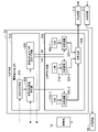
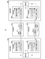
- FIG. 1 is a block diagram showing a configuration of an optical transmission system 1 according to the first embodiment.
- the optical transmission system 1 includes optical communication devices 2A and 2B and optical transmission lines 3-1 and 3-2.
- the optical communication device 2A is referred to as a first optical communication device
- the optical communication device 2B is also referred to as a second optical communication device.
- the optical transmission line 3-1 is a transmission line that transmits an optical signal transmitted by the optical communication device 2A to the optical communication device 2B.
- the optical transmission line 3-2 is a transmission line that transmits an optical signal transmitted by the optical communication device 2B to the optical communication device 2A.
- the solid line connecting the optical communication device 2A and the optical communication device 2B propagates an optical signal related to data transmitted / received via the optical transmission lines 3-1 and 3-2. It is a connecting line.
- the broken line connection line is a connection line through which electrical signals related to control transmitted and received by the control units 7A and 7B propagate. The meanings of these line types are the same in FIGS. 2, 5, 6, 8, and 16 to 18 after FIG. 1.
- Each of the optical transmission lines 3-1 and 3-2 includes optical fibers 31-1 and 31-2 and optical amplifiers 32-1 and 32-2. It is assumed that the optical fiber 31-1 and the optical fiber 31-2 are transmission media of optical signals having the same properties. It is assumed that the distance between the optical transmission line 3-1 and the optical transmission line 3-2 is the same. Therefore, it is assumed that the wavelength dispersion effect generated in the optical transmission line 3-1 and the optical transmission line 3-2 is the same.
- Each of the optical amplifiers 32-1 and 32-2 included in each of the optical transmission lines 3-1 and 3-2 is connected to the optical fibers 31-1 and 31-2, and the optical fibers 31-1 and 31- The optical signal propagating in each of 2 is amplified.
- the configuration shown in the optical transmission paths 3-1 and 3-2 is an example.
- the optical amplifier 32-1 may be inserted in the middle of the optical fiber 31-1 or the optical fiber 31-2.
- An optical amplifier 32-2 may be inserted in the middle of the optical fiber, or a device such as an optical switch or a reproduction repeater other than the optical amplifiers 32-1 and 32-2 may be connected to the optical fibers 31-1 and 31-2. It may be inserted in the middle of the optical fibers 31-1 and 31-2.
- the optical communication device 2A includes an optical transmission unit 5A, an optical reception unit 6A, and a control unit 7A.
- the optical transmission unit 5A includes an electrical signal generation unit 51A and an optical signal generation unit 52A.
- the electric signal generation unit 51A includes a wavelength dispersion amount calculation signal generation unit 81A, a main signal generation unit 82A, and a wavelength dispersion compensation processing unit 83A.
- the signal generation unit 81A for calculating the wavelength dispersion amount calculates the wavelength dispersion amount, which is a digital electric signal at a transmission rate that establishes synchronization with the optical communication device 2B without performing wavelength dispersion compensation in the optical transmission path 3-1. Signals for 2 channels are generated and output at the same transmission rate.
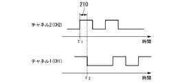
- Each of the wavelength dispersion amount calculation signals of the two channels is, for example, as shown in FIG. 3, a pulse signal of a different NRZ (Non Return to Zero) system.
- the signal for calculating the wavelength dispersion amount may be a pulse signal other than the NRZ method as long as the timing of the pulse change can be clearly detected.
- the signal generation unit 81A for calculating the wavelength dispersion amount is for calculating the wavelength dispersion amount of the two channels so that the timings at which the pulses in the wavelength dispersion amount calculation signals of the two channels change match. Generate a signal.
- the wavelength dispersion amount calculation signal generation unit 81A generates the wavelength dispersion amount calculation signal
- the wavelength dispersion amount calculation signal is generated by including a specific synchronization data pattern for detecting synchronization at the beginning.
- the main signal generation unit 82A encodes the data to be transmitted to the optical communication device 2B to generate a main signal which is a digital electric signal.
- the main signal is generated by including a specific synchronization data pattern for detecting synchronization at the beginning.
- the specific synchronization data pattern included when the main signal generation unit 82A generates the main signal is different from the synchronization data pattern of the wavelength dispersion amount calculation signal.
- the transmission rate of the main signal generated by the main signal generation unit 82A is higher than the transmission rate of the signal for calculating the wavelength dispersion amount, and when the wavelength dispersion compensation is not performed, synchronization with the optical communication device 2B is performed. The transmission rate is not established.
- the wavelength dispersion compensation processing unit 83A performs wavelength dispersion compensation for the main signal output by the main signal generation unit 82A based on the wavelength dispersion amount of the optical transmission line 3-1 calculated by the optical communication device 2B.
- the optical signal generation unit 52A includes a light source 91A-1, 91A-2, 91A-3, an optical modulator 92A-1, 92A-2, 92A-3, and an optical coupler 90A.
- the light source 91A-1 emits light having a wavelength of ⁇ 1 .
- the light source 91A-2 emits light having a wavelength of ⁇ 2 .
- the light source 91A-3 emits light having a wavelength of ⁇ 3 .
- the optical coupler 90A is, for example, an optical coupler, which is connected to the output side of each of the optical modulators 92A-1, 92A-2, and 92A-3 via an optical fiber, and is connected to the optical transmission line 3- via the optical fiber. Connect to 1.
- one channel of the two channels of the wavelength dispersion amount calculation signal generated by the wavelength dispersion amount calculation signal generation unit 81A (hereinafter, the channel is referred to as “channel 1 or CH (Channel) 1”). ”), The light of wavelength ⁇ 1 emitted by the light source 91A-1 is modulated to generate an optical signal of the wavelength dispersion amount calculation signal of channel 1.
- the other channel of the two-channel wavelength dispersion amount calculation signal generated by the wavelength dispersion amount calculation signal generation unit 81A (hereinafter, the channel is referred to as “channel 2 or CH (Channel) 2”). ”),
- the light of wavelength ⁇ 2 emitted by the light source 91A-2 is modulated to generate an optical signal of the wavelength dispersion amount calculation signal of channel 2.
- the optical coupler 90A is an optical signal of a signal for calculating the wavelength dispersion amount of channel 1 generated by the light modulator 92A-1 and an optical signal of a signal for calculating the wavelength dispersion amount of channel 2 generated by the light modulator 92A-2. Is combined and sent to the optical transmission path 3-1.
- the light modulator 92A-3 modulates the light of the wavelength ⁇ 3 emitted by the light source 91A-3 based on the main signal of the wavelength dispersion compensation processing unit 83A to generate the optical signal of the main signal.
- the light modulator 92A-3 sends the generated optical signal of wavelength ⁇ 3 to the optical transmission line 3-1 via the optical coupler 90A.
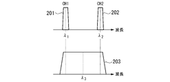
- FIG. 4 shows the optical signal spectrum 201 of the wavelength dispersion calculation signal of the channel 1 of the wavelength ⁇ 1 generated by the optical modulator 92A-1 and the channel 2 of the wavelength ⁇ 2 generated by the optical modulator 92A-2.
- 6 is a graph showing the relationship between the optical signal spectrum 202 of the wavelength dispersion amount calculation signal and the optical signal spectrum 203 of the main signal having the wavelength ⁇ 3 generated by the optical modulator 92A-3.
- the horizontal axis of the two graphs shown in FIG. 4 is the wavelength, and the vertical axis is the light intensity.
- the spectrum 201 of the optical signal of the wavelength dispersion amount calculation signal of channel 1 has a center wavelength of ⁇ 1
- 202 has a center wavelength of ⁇ 2
- the spectrum 203 of the optical signal of the main signal has a center wavelength of ⁇ 3 .
- the wavelength dispersion amount calculation signals of channel 1 and channel 2 have the same transmission rate. Therefore, the spreads of the spectra 201 and 202 are the same, which is lower than the transmission rate of the main signal, and therefore narrower than the spread of the spectra 203 of the optical signal of the main signal.
- ⁇ 2 needs to be predetermined.
- the range of the wavelength ⁇ 1 which is the minimum center wavelength and the wavelength ⁇ 2 which is the maximum center wavelength should be maximized.
- the wavelength ⁇ 1 and the wavelength ⁇ 2 need to be predetermined.
- the transmission rate of the wavelength dispersion amount calculation signal, the wavelength ⁇ 1 and the wavelength ⁇ 2 are predetermined so as not to prevent the wavelength dispersion amount from being calculated. Therefore, in the optical transmission line 3-1 each of the optical signals of the wavelength dispersion amount calculation signal of the channel 1 and the channel 2 does not interfere with each other.
- the optical transmission unit 5A does not transmit the optical signal of the main signal to the optical transmission line 3-1 during the period in which the optical signal of the signal for calculating the wavelength dispersion amount of channel 1 and channel 2 is transmitted to the optical transmission line 3-1. Therefore, the optical signal of the signal for calculating the wavelength dispersion amount of the channel 1 and the channel 2 and the optical signal of the main signal do not interfere with each other in the optical transmission line 3-1.
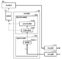
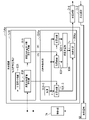
- the optical receiving unit 6A includes an optical signal receiving unit 61A and an electric signal processing unit 62A. As shown in FIG. 5, the optical signal receiving unit 61A includes a demodulator 102A-3.
- the demodulator 102A-3 is connected to the optical transmission line 3-2 via an optical fiber, and demodulates the main signal of the digital electric signal from the optical signal of the wavelength ⁇ 3 transmitted by the optical transmission line 3-2. ..
- the demodulation is, for example, when the optical signal of the main signal is generated by intensity modulation, the optical signal is directly detected and converted into a digital electric signal.
- the electric signal processing unit 62A includes a main signal processing unit 112A and a synchronization determination unit 114A.
- the synchronization determination unit 114A determines whether or not synchronization can be established based on the main signal demodulated by the demodulator 102A-3 from the optical signal having the wavelength ⁇ 3 .
- the determination as to whether or not synchronization can be established is performed, for example, by whether or not a specific synchronization data pattern included at the beginning of the main signal is detected.
- the synchronization determination unit 114A determines that synchronization can be established when a specific synchronization data pattern is detected, and determines that synchronization cannot be established when a specific synchronization data pattern is not detected.
- the synchronization determination unit 114A determines that synchronization can be established, it outputs the captured main signal to the main signal processing unit 112A.
- the captured main signal is not output to the main signal processing unit 112A, and the synchronization failure notification signal indicating that synchronization cannot be established is output to the control unit 7A. do.
- the main signal processing unit 112A decodes the main signal output by the synchronization determination unit 114A and reads out the data contained in the main signal.
- the main signal processing unit 112A outputs the read data to the control unit 7A.
- the control unit 7A is used for each of the electric signal generation unit 51A and the optical signal generation unit 52A of the optical transmission unit 5A, and the optical signal reception unit 61A and the electric signal processing unit 62A of the optical reception unit 6A. It is connected and performs a process of controlling the operation of the electric signal generation unit 51A, the optical signal generation unit 52A, the optical signal reception unit 61A, and the electric signal processing unit 62A.
- the control unit 7A receives an instruction to start the process of calculating the wavelength dispersion amount by the operation of the user of the optical transmission system 1
- the control unit 7A outputs the start instruction signal to the wavelength dispersion amount calculation signal generation unit 81A.
- the control unit 7A captures the data output by the main signal processing unit 112A, and when the captured data is data indicating the wavelength dispersion amount, outputs the data indicating the wavelength dispersion compensation amount to the wavelength dispersion compensation processing unit 83A. An end instruction signal indicating that the process of calculating the wavelength dispersion amount is terminated is output to the wavelength dispersion amount calculation signal generation unit 81A.
- the control unit 7A If the captured data is not data indicating the amount of wavelength dispersion, the control unit 7A outputs the captured data to the outside. When the control unit 7A receives the synchronization failure notification signal from the synchronization determination unit 114A, the control unit 7A notifies the user of the optical transmission system 1 that synchronization of the main signal could not be established in the optical transmission line 3-2. do. When arbitrary data to be transmitted to the optical communication device 2B is given from the outside, the control unit 7A outputs the given data to the main signal generation unit 82A.
- the optical communication device 2B includes an optical receiving unit 6B, an optical transmitting unit 5B, and a control unit 7B.
- the optical receiving unit 6B includes an optical signal receiving unit 61B and an electric signal processing unit 62B.
- the optical signal receiving unit 61B includes an optical bandpass filter unit 101B-1, 101B-2, a demodulator 102B-1, 102B-2, 102B-3, and an optical turnout 100B.
- the optical branching device 100B is, for example, an optical coupler, and is connected to each input side of the optical band path filter units 101B-1 and 101B-2 and the input side of the demodulator 102B-3 via an optical fiber. It is connected to the optical transmission line 3-1 via an optical fiber.
- the optical branching device 100B receives the optical signal transmitted by the optical transmission path 3-1 and branches into three, and each of the three branched optical signals is combined with the optical band path filter units 101B-1 and 101B-2. , Output to demodulator 102B-3.
- the optical bandpass filter unit 101B-1 captures the optical signal output by the optical branching device 100B, filters the captured optical signal by the bandpass, and outputs an optical signal having a constant wavelength width centered on the wavelength ⁇ 1. ..
- the optical bandpass filter unit 101B-2 captures the optical signal output by the optical branching device 100B, filters the captured optical signal by the bandpass, and outputs an optical signal having a constant wavelength width centered on the wavelength ⁇ 2 . ..
- the range of a certain wavelength width in the optical bandpass filter units 101B-1 and 101B-2 is the same as or almost the same as the wavelength width of the spectra 201 and 202 shown in FIG. That is, the size of the range of a certain wavelength width in the optical bandpass filter units 101B-1 and 101B-2 is a size predetermined according to the transmission rate of the wavelength dispersion amount calculation signal of the channel 1 and the channel 2. ..
- the demodulator 102B-1 demodulates the wavelength dispersion amount calculation signal of channel 1, which is a digital electric signal, from the optical signal of wavelength ⁇ 1 output by the optical band path filter unit 101B-1.
- the demodulator 102B-2 demodulates the wavelength dispersion amount calculation signal of channel 2, which is a digital electric signal, from the optical signal of wavelength ⁇ 2 output by the optical band path filter unit 101B-2.
- the demodulator 102B-3 demodulates the main signal of the digital electric signal from the optical signal output by the optical turnout 100B.
- the electric signal processing unit 62B includes a wavelength dispersion amount calculation unit 111B, a main signal processing unit 112B, a synchronization determination unit 113B, and a synchronization determination unit 114B.
- the synchronization determination unit 113B includes a signal for calculating the wavelength dispersion amount of channel 1 demodrated by the demodulator 102B-1 from the optical signal of wavelength ⁇ 1 and the channel 2 demodled by the demodulator 102B-2 from the optical signal of wavelength ⁇ 2 . Based on the wavelength dispersion amount calculation signal, it is determined whether or not synchronization can be established in both the wavelength dispersion amount calculation signal of channel 1 and channel 2.
- the determination of whether or not synchronization can be established depends on, for example, whether or not a specific synchronization data pattern included at the beginning of both the wavelength dispersion amount calculation signals of channel 1 and channel 2 is detected. Will be done.
- the synchronization determination unit 113B detects a specific synchronization data pattern from both the wavelength dispersion amount calculation signals of channel 1 and channel 2, it determines that synchronization can be established, and calculates the wavelength dispersion amount of channel 1 and channel 2. If a specific synchronization data pattern is not detected from either one or both of the signals, it is determined that synchronization cannot be established.
- the synchronization determination unit 113B determines that synchronization can be established, it outputs the captured channel 1 and channel 2 wavelength dispersion amount calculation signals to the wavelength dispersion amount calculation unit 111B.
- the synchronization determination unit 113B determines that synchronization cannot be established, the synchronization determination unit 113B outputs a synchronization failure notification signal including information for identifying the channel for which synchronization could not be established to the control unit 7B.
- the wavelength dispersion amount calculation unit 111B is affected by the wavelength dispersion effect while propagating through the optical transmission path 3-1 so that the optical signal of the wavelength dispersion amount calculation signal of channel 1 of wavelength ⁇ 1 and the wavelength ⁇ 2
- the wavelength dispersion amount is calculated from the time difference in propagation between the optical signal and the optical signal of the wavelength dispersion amount calculation signal of channel 2.
- the wavelength dispersion amount calculation unit 111B calculates the delay time represented by reference numeral 210 from the following equation (1).
- the wavelength dispersion amount calculation unit 111B previously stores the wavelength ⁇ 1 which is the center wavelength of the wavelength dispersion amount calculation signal of channel 1 and the wavelength ⁇ 2 which is the center wavelength of the wavelength dispersion amount calculation signal of channel 2 in the internal storage area. I remember that.
- the unit of the wavelengths ⁇ 1 and ⁇ 2 is, for example, [nm (nano-meter)].
- the wavelength dispersion amount calculation unit 111B calculates the wavelength dispersion amount D [psec / nm] by the following equation (2) based on the calculated delay time and the wavelengths ⁇ 1 and ⁇ 2 stored in the internal storage area.
- the synchronization determination unit 114B has the synchronization determination unit 114A of the optical communication device 2A shown in FIG. 5, except that the connection destination is the demodulator 102B-3 and the main signal processing unit 112B.
- the main signal processing unit 112B has the same configuration as the main signal processing unit 112A of the optical communication device 2A shown in FIG. 5, except that the connection destination is the control unit 7B and the synchronization determination unit 114B. It has the same configuration.
- the optical transmission unit 5B includes an electrical signal generation unit 51B and an optical signal generation unit 52B.
- the electric signal generation unit 51B includes a main signal generation unit 82B and a wavelength dispersion compensation processing unit 83B.
- the main signal generation unit 82B has the same configuration as the main signal generation unit 82A of the optical communication device 2A shown in FIG. 2, except that the connection destination is the control unit 7B and the wavelength dispersion compensation processing unit 83B. Be prepared.
- the wavelength dispersion compensation processing unit 83B has a configuration in which the connection destinations are the main signal generation unit 82B, the control unit 7B, and the optical modulator 92B-3, and the wavelength dispersion of the optical communication device 2A shown in FIG. It has the same configuration as the compensation processing unit 83A.
- the optical signal generation unit 52B includes a light source 91B-3 and an optical modulator 92B-3.
- the light source 91B-3 emits light having a wavelength ⁇ 3 like the light source 91A-3 of the optical communication device 2A shown in FIG.
- the light modulator 92B-3 modulates the light of the wavelength ⁇ 3 emitted by the light source 91B-3 based on the main signal of the wavelength dispersion compensation processing unit 83B to generate the optical signal of the main signal.
- the light modulator 92B-3 is connected to the optical transmission line 3-2 via an optical fiber, and sends the generated optical signal of wavelength ⁇ 3 to the optical transmission line 3-2.
- control unit 7B is used for each of the optical signal receiving unit 61B and the electric signal processing unit 62B of the optical receiving unit 6B, and the electric signal generation unit 51B and the optical signal generation unit 52B of the optical transmission unit 5B. It connects and performs a process of controlling the operation of the optical signal receiving unit 61B, the electric signal processing unit 62B, the electric signal generation unit 51B, and the optical signal generation unit 52B.
- the control unit 7B captures data indicating the wavelength dispersion amount D output by the wavelength dispersion amount calculation unit 111B, and inputs the captured data indicating the wavelength dispersion amount D to the main signal generation unit 82B and the wavelength dispersion compensation processing unit 83B. Output.
- the control unit 7B receives a synchronization non-establishment notification signal from the synchronization determination unit 113B including information specifying a channel for which synchronization could not be established
- the control unit 7B informs the user of the optical transmission system 1 that the optical transmission line 3-1. Notifies that the synchronization of the signal for calculating the wavelength dispersion amount could not be established, and also notifies the information specifying the channel for which synchronization could not be established.
- the control unit 7B receives the synchronization failure notification signal from the synchronization determination unit 114B, the control unit 7B notifies the user of the optical transmission system 1 that synchronization of the main signal could not be established in the optical transmission line 3-1. do.
- control unit 7B When the control unit 7B captures the data output by the main signal processing unit 112B, the control unit 7B outputs the captured data to the outside. When arbitrary data to be transmitted to the optical communication device 2A is given from the outside, the control unit 7B outputs the given data to the main signal generation unit 82B.
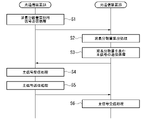
- FIG. 9 is a sequence diagram showing the entire flow of the process of performing wavelength dispersion compensation by the optical transmission system 1.
- the optical transmission unit 5A of the optical communication device 2A performs a signal generation process for calculating the wavelength dispersion amount (step S1).
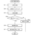
- FIG. 10 is a flowchart showing the details of the process of step S1.
- the control unit 7A of the optical communication device 2A receives an instruction to start the process of calculating the wavelength dispersion amount by the operation of the user of the optical transmission system 1, the start instruction signal is sent to the wavelength dispersion amount calculation signal generation unit 81A.
- Output step S1-1
- the wavelength dispersion amount calculation signal generation unit 81A receives the start instruction signal from the control unit 7A, the wavelength dispersion amount calculation signal is generated for channel 1 and channel 2, and the generated wavelength dispersion amount calculation signal for channel 1 is generated. It is output to the optical modulator 92A-1, and the generated signal for calculating the wavelength dispersion amount of the channel 2 is output to the optical modulator 92A-2 (step S1-2).
- the optical modulator 92A-1 captures the wavelength dispersion calculation signal of channel 1 output by the wavelength dispersion calculation signal generation unit 81A, and based on the captured channel 1 wavelength dispersion calculation signal, the light source 91A- The light of the wavelength ⁇ 1 emitted by 1 is modulated to generate the optical signal of the wavelength dispersion amount calculation signal of the channel 1.
- the light modulator 92A-1 outputs the optical signal of the generated wavelength dispersion amount calculation signal of the channel 1 of the wavelength ⁇ 1 to the optical coupler 90A.
- the optical modulator 92A-2 captures the wavelength dispersion calculation signal of channel 2 output by the wavelength dispersion calculation signal generation unit 81A, and based on the captured channel 2 wavelength dispersion calculation signal, the light source 91A- The light of wavelength ⁇ 2 emitted by 2 is modulated to generate an optical signal of a signal for calculating the wavelength dispersion amount of channel 2.
- the light modulator 92A-2 outputs the optical signal of the generated wavelength dispersion amount calculation signal of the channel 2 of the wavelength ⁇ 2 to the optical coupler 90A (step S1-3).
- the optical coupler 90A takes in the optical signal of the wavelength dispersion amount calculation signal of the channel 1 of the wavelength ⁇ 1 output by the optical modulator 92A-1, and outputs the optical signal of the channel 2 of the wavelength ⁇ 2 output by the optical modulator 92A-2.
- the optical signal of the wavelength dispersion amount calculation signal is captured, and the two captured optical signals are combined and transmitted to the optical transmission path 3-1 (step S1-4).
- the wavelength dispersion amount calculation signal generation unit 81A determines whether or not an end instruction signal indicating that the process of calculating the wavelength dispersion amount is terminated is received from the control unit 7A (step S1-5). When it is determined that the wavelength dispersion amount calculation signal generation unit 81A has not received the end instruction signal from the control unit 7A (steps S1-5, No), the processing of steps S1-2 and subsequent steps is performed again.
- FIG. 11 is a flowchart showing the details of the process of step S2.
- the optical branching device 100B receives the optical signal transmitted by the optical transmission path 3-1 and branches the received optical signal into three, the demodulator 102B-3 and the optical band path filter units 101B-1, 101B. Output to -2 (step S2-1).
- the optical bandpass filter unit 101B-1 captures the optical signal output by the optical branching device 100B, filters the captured optical signal, and demodulates an optical signal having a certain wavelength width centered on the wavelength ⁇ 1. Output to.
- the optical band path filter unit 101B-2 captures the optical signal output by the optical branching device 100B, filters the captured optical signal, and produces an optical signal having a certain wavelength width centered on the wavelength ⁇ 2 demodulator 102B-2. Is output to (step S2-2).
- the demodulator 102B-1 demodulates the wavelength dispersion amount calculation signal of channel 1, which is a digital electric signal, from the optical signal output by the optical bandpass filter unit 101B-1.
- the demodulator 102B-1 outputs the demodulated channel 1 wavelength dispersion amount calculation signal to the synchronization determination unit 113B.
- the demodulator 102B-2 demodulates the wavelength dispersion amount calculation signal of channel 2, which is a digital electric signal, from the optical signal output by the optical bandpass filter unit 101B-2.
- the demodulator 102B-2 outputs the demodulated channel 2 wavelength dispersion amount calculation signal to the synchronization determination unit 113B (step S2-3).
- the synchronization determination unit 113B takes in the wavelength dispersion amount calculation signal of channel 1 output by the demodulator 102B-1 and the wavelength dispersion amount calculation signal of channel 2 output by the demodulator 102B-2.
- the synchronization determination unit 113B synchronizes both the wavelength dispersion amount calculation signal of the channel 1 and the channel 2 based on the captured channel 1 wavelength dispersion amount calculation signal and the channel 2 wavelength dispersion amount calculation signal. It is determined whether or not it can be established (step S2-4).
- the synchronization determination unit 113B When it is determined that synchronization cannot be established (step S2-4, No), the synchronization determination unit 113B outputs a synchronization failure notification signal including information for identifying the channel for which synchronization could not be established to the control unit 7B.
- the control unit 7B takes in the synchronization failure notification signal output by the synchronization determination unit 113B, and cannot establish synchronization of the wavelength dispersion amount calculation signal in the optical transmission line 3-1 for the user of the optical transmission system 1. Not only that, but also the information for identifying the channel for which synchronization could not be established included in the synchronization failure notification signal is notified (step S2-5), and the process ends.
- the synchronization determination unit 113B outputs the captured channel 1 and channel 2 wavelength dispersion amount calculation signal to the wavelength dispersion amount calculation unit 111B.
- the wavelength dispersion amount calculation unit 111B captures the wavelength dispersion amount calculation signals of channel 1 and channel 2 output by the synchronization determination unit 113B, and the equation (1) is based on the wavelength dispersion amount calculation signals of the captured channels 1 and 2. ) To calculate the delay time (step S2-6).
- the wavelength dispersion amount calculation unit 111B calculates the wavelength dispersion amount D [psec / nm] by the equation (2) based on the calculated delay time and the wavelengths ⁇ 1 and ⁇ 2 stored in the internal storage area.
- the wavelength dispersion amount calculation unit 111B outputs the data indicating the calculated wavelength dispersion amount D to the control unit 7B (step S2-7), and ends the process.
- the demodulator 102B-3 for the main signal captures and captures the optical signals of the signals for calculating the wavelength dispersion amount of channel 1 and channel 2 output by the optical branching device 100B at the timing of step S2-1. Is demodulated into an electric signal and output to the synchronization determination unit 114B.
- the demodulator 102B-3 since the optical signal of the signal for calculating the wavelength dispersion amount of channel 1 and channel 2 is not a normal main signal having the wavelength ⁇ 3 as the central wavelength, the demodulator 102B-3 has the wavelength dispersion amount of channel 1 and channel 2.
- the optical signal of the calculation signal cannot be demodulated normally, and the electric signal demodulated by the demodulator 102B-3 does not include a specific synchronization data pattern corresponding to the main signal.
- the synchronization determination unit 114B does not determine that synchronization can be established based on the electric signal demodulated by the demodulator 102B-3, and outputs the electric signal demodulated by the demodulator 102B-3 to the main signal processing unit 112B. There is no such thing.
- FIG. 12 is a flowchart showing the details of the process of step S3.
- the control unit 7B captures data indicating the wavelength dispersion amount D output by the wavelength dispersion amount calculation unit 111B in the process of step S2-7, and the captured data indicating the wavelength dispersion amount D is wavelength-dispersed with the main signal generation unit 82B. It is output to the compensation processing unit 83B.
- the main signal generation unit 82B takes in data indicating the wavelength dispersion amount D output by the control unit 7B.
- the wavelength dispersion compensation processing unit 83B takes in the data indicating the wavelength dispersion amount D output by the control unit 7B, and writes and stores the data indicating the captured wavelength dispersion amount D in the internal storage area (step S3-1).
- the main signal generation unit 82B encodes the data indicating the wavelength dispersion amount D to generate the main signal.
- the main signal generation unit 82B outputs the generated main signal to the wavelength dispersion compensation processing unit 83B (step S3-2).
- the wavelength dispersion compensation processing unit 83B captures the main signal including the data indicating the wavelength dispersion amount D output by the main signal generation unit 82B, and internally stores the main signal including the data indicating the captured wavelength dispersion amount D. Wavelength dispersion compensation is performed based on the wavelength dispersion amount D stored in the region.
- the wavelength dispersion compensation processing unit 83B outputs a main signal including data indicating the wavelength dispersion amount D for which the wavelength dispersion is compensated to the light modulator 92B-3 (step S3-3).
- the optical modulator 92B-3 modulates the light of the wavelength ⁇ 3 emitted by the light source 91B-3 based on the main signal including the data indicating the wavelength dispersion amount D of the wavelength dispersion compensation processing unit 83B.
- An optical signal of the main signal is generated (step S3-4).
- the light modulator 92B-3 sends an optical signal of the generated main signal of wavelength ⁇ 3 to the optical transmission line 3-2 (step S3-5), and ends the process.
- FIG. 13 is a flowchart showing the details of the process of step S4.
- the demodulator 102A-3 of the optical receiving unit 6A of the optical communication device 2A receives the optical signal of the main signal of the wavelength ⁇ 3 transmitted by the optical transmission path 3-2, and is the main digital electric signal from the received optical signal. Demote the signal.
- the demodulator 102A-3 outputs the demodulated main signal to the synchronization determination unit 114A (step S4-1).
- the synchronization determination unit 114A captures the main signal output by the demodulator 102A-3, and determines whether or not synchronization can be established based on the captured main signal (step S4-2).
- step S4-2 When it is determined that synchronization cannot be established (step S4-2, No), the synchronization determination unit 114A outputs a synchronization non-establishment notification signal indicating that synchronization could not be established to the control unit 7A.
- the control unit 7A takes in the synchronization failure notification signal output by the synchronization determination unit 114A, and notifies the user of the optical transmission system 1 that synchronization of the main signal could not be established in the optical transmission line 3-2. Then (step S4-3), the process is terminated.
- the synchronization determination unit 114A outputs the captured main signal to the main signal processing unit 112A.
- the main signal processing unit 112A captures the main signal output by the synchronization determination unit 114A, decodes the captured main signal, reads out the data indicating the wavelength dispersion amount D, and outputs the data indicating the read wavelength dispersion amount D to the control unit 7A. Is output to (step S4-4).
- the control unit 7A captures the data output by the main signal processing unit 112A, and determines whether or not the captured data is data indicating the wavelength dispersion amount D (step S4-5). Here, since the data output by the main signal processing unit 112A is the data indicating the wavelength dispersion amount D, the control unit 7A determines that the captured data is the data indicating the wavelength dispersion amount D (step S4-). 5, Yes).
- the control unit 7A outputs data indicating the wavelength dispersion amount D to the wavelength dispersion compensation processing unit 83A of the optical transmission unit 5A (step S4-6).
- the wavelength dispersion compensation processing unit 83A takes in the data indicating the wavelength dispersion amount D output by the control unit 7A, and writes and stores the data indicating the captured wavelength dispersion amount D in the internal storage area.
- the control unit 7A outputs an end instruction signal indicating that the process of calculating the wavelength dispersion amount is terminated to the wavelength dispersion amount calculation signal generation unit 81A of the optical transmission unit 5A (step S4-7), and ends the process. do.
- the wavelength dispersion amount calculation signal generation unit 81A determines that the end instruction signal has been received as shown in step S1-5 of FIG. 10 (step S1). -5, Yes), the signal transmission process for calculating the wavelength dispersion amount shown in FIG. 10 is completed.
- step S4-5 determines in step S4-5 that the captured data is not the data indicating the wavelength dispersion amount D (steps S4-5, No)
- the control unit 7A outputs the captured data to the outside (step S4). -8), the process is terminated.
- data indicating the wavelength dispersion amount D is stored in the storage areas inside both the wavelength dispersion compensation processing units 83A and 83B of the optical communication devices 2A and 2B, and the optical transmission path 3 is stored from the optical communication device 2B. Synchronization will be established in the path for transmitting the main signal to the optical communication device 2A via -2.
- step S5 the control unit 7A and the optical transmission unit 5A of the optical communication device 2A perform a main signal transmission process of transmitting arbitrary data by a main signal (step S5).
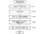
- FIG. 14 is a flowchart showing the details of the process of step S5.
- the control unit 7A takes in the given data and outputs the taken-in data to the main signal generation unit 82A.
- the main signal generation unit 82A captures the data output by the control unit 7A (step S5-1).
- the main signal generation unit 82A encodes the captured data to generate a main signal.
- the main signal generation unit 82A outputs the generated main signal to the wavelength dispersion compensation processing unit 83A (step S5-2).
- the wavelength dispersion compensation processing unit 83A captures the main signal output by the main signal generation unit 82A, and performs wavelength dispersion compensation based on the wavelength dispersion amount D stored in the internal storage area for the captured main signal.
- the wavelength dispersion compensation processing unit 83A outputs the wavelength dispersion compensated main signal to the light modulator 92A-3 (step S5-3).
- the light modulator 92A-3 modulates the light of the wavelength ⁇ 3 emitted by the light source 91A-3 based on the main signal of the wavelength dispersion compensation processing unit 83A to generate the optical signal of the main signal (the optical modulator of the main signal is generated. Step S5-4).
- the light modulator 92A-3 sends the generated optical signal having a wavelength ⁇ 3 to the optical transmission line 3-1 via the optical coupler 90A (step S5-5), and ends the process.
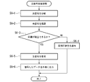
- FIG. 15 is a flowchart showing the details of the process of step S6.
- the optical branching device 100B receives the optical signal transmitted by the optical transmission path 3-1 and branches the received optical signal into three, the demodulator 102B-3 and the optical band path filter units 101B-1, 101B. Output to -2 (step S6-1).
- the demodulator 102B-3 demodulates the main signal of the digital electric signal from the optical signal transmitted by the optical transmission line 3-1 (step S6-2).
- the demodulator 102B-3 outputs the demodulated main signal to the synchronization determination unit 114B.
- the synchronization determination unit 114B takes in the main signal output by the demodulator 102B-3.
- the synchronization determination unit 114B determines whether or not synchronization can be established based on the captured main signal (step S6-3).
- step S6-3 When it is determined that synchronization cannot be established (step S6-3, No), the synchronization determination unit 114B outputs a synchronization non-establishment notification signal indicating that synchronization could not be established to the control unit 7B.
- the control unit 7B takes in the synchronization failure notification signal output by the synchronization determination unit 114B, and notifies the user of the optical transmission system 1 that the synchronization of the main signal could not be established in the optical transmission line 3-1. Then (step S6-4), the process is terminated.
- the synchronization determination unit 114B outputs the captured main signal to the main signal processing unit 112B.
- the main signal processing unit 112B captures the main signal output by the synchronization determination unit 114B, decodes the captured main signal, reads the data, and outputs the read data to the control unit 7B (step S6-5).
- the control unit 7B captures the data output by the synchronization determination unit 114B, outputs the captured data to the outside (step S6-6), and ends the process.
- the wavelength width of the spectrum of the optical signal of the main signal having the wavelength ⁇ 3 transmitted by the optical transmission line 3-1 includes the wavelengths ⁇ 1 and ⁇ 2 . Therefore, at the timing of step S6-2, each of the optical bandpass filter units 101B-1 and 101B-2 extracts the optical signal of the main signal that the optical branching device 100B branches and outputs by filtering. A part of the optical signal of the main signal is output to the demodulators 102B-1 and 102B-2 corresponding to each. However, since the demodulators 102B-1 and 102B-2 demodulate a part of the optical signal of the main signal, the main signal cannot be demodulated normally, and the demodulators 102B-1 and 102B-2 do not.
- the demodulated electric signal does not include a synchronization data pattern corresponding to the signal for calculating the amount of wavelength dispersion. Therefore, the synchronization determination unit 113B does not determine that synchronization can be established based on the electric signals demodulated by the demodulators 102B-1 and 102B-2, and the demodulators 102B-1 and 102B-2 demodulate the electric signals. It is not output to the wavelength dispersion amount calculation unit 111B.
- control unit 7A Main signal generation unit 82A, wavelength dispersion compensation processing unit 83A, light source 91A-3 and optical modulator 92A-3 perform the same processing as control unit 7B, main signal generation unit 82B, wavelength dispersion compensation processing unit 83B. , Light source 91B-3 and light modulator 92B-3.
- the demodulator 102A-3 receives the optical signal transmitted by the optical transmission path 3-2, and is step S6-1 of the processes of steps S6-1 to S6-6 shown in FIG.
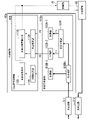
- FIG. 16 is a block diagram showing a configuration of the optical transmission system 1a of the second embodiment.
- the optical transmission system 1a includes optical communication devices 2Aa and 2Ba.
- the optical communication device 2Aa includes an optical transmission unit 5Aa, an optical reception unit 6A, and a control unit 7A.
- the optical communication device 2Ba includes an optical receiving unit 6Ba, an optical transmitting unit 5B, and a control unit 7B.
- the optical transmission unit 5Aa included in the optical communication device 2Aa includes an electrical signal generation unit 51A and an optical signal generation unit 52Aa.
- the optical signal generation unit 52Aa includes a light source 91A-3, an optical modulator 92A-1, 92A-2, 92A-3, a wavelength division multiplexing unit 93A, and an optical coupler 90Aa.
- the light source 91A-3 is a light source that emits light having a wavelength ⁇ 3 which is the wavelength of the main signal, like the light source 91A-3 of the first embodiment, and in the second embodiment, the light modulator 92A- Light is emitted to each of 1 to 92A-3.
- the wavelength multiplexing unit 93A converts the optical signal of the wavelength dispersion amount calculation signal of the channel 1 of the wavelength ⁇ 3 output by the optical modulator 92A-1 into the optical signal of the wavelength ⁇ 1 , and the optical modulator 92A-2 outputs it.
- the optical signal of the wavelength dispersion amount calculation signal of the channel 2 of the wavelength ⁇ 3 is converted into the optical signal of the wavelength ⁇ 2 .
- the optical coupler 90Aa is, for example, an optical coupler, which is connected to the output side of the wavelength multiplexing unit 93A and the output side of the optical modulator 92A-3 via an optical fiber, and is connected to the optical transmission line 3 via the optical fiber. Connect to -1.
- the optical receiving unit 6Ba of the optical communication device 2Ba includes an optical signal receiving unit 61Ba and an electric signal processing unit 62B. As shown in FIG. 18, the optical signal receiving unit 61Ba includes demodulators 102B-1, 102B-2, 102B-3, a wavelength separation unit 103B, and an optical turnout 100Ba.
- the optical branching device 100Ba is, for example, an optical coupler, which is connected to the input side of the wavelength separator 103B and the input side of the demodulator 102B-3 via an optical fiber, and is connected to the optical transmission line 3- via the optical fiber. Connect to 1.
- the optical branching device 100Ba branches the optical signal transmitted by the optical transmission line 3-1 into two, and outputs each of the two branched optical signals to the wavelength separator 103B and the demodulator 102B-3.
- the wavelength separation unit 103B captures the optical signal output by the optical branching device 100Ba, and separates the captured optical signal into an optical signal having a wavelength ⁇ 1 and an optical signal having a wavelength ⁇ 2 .
- the wavelength separation unit 103B sets the wavelength of the separated optical signal of wavelength ⁇ 1 to wavelength ⁇ 3 and outputs it to the demodulator 102B-1, and sets the wavelength of the separated optical signal of wavelength ⁇ 2 to wavelength ⁇ 3 and outputs the demodulator 102B. Output to -2.
- the optical modulator 92A-1 captures the wavelength dispersion calculation signal of channel 1 output by the wavelength dispersion calculation signal generation unit 81A, and based on the captured channel 1 wavelength dispersion calculation signal, the light source 91A- The light of the wavelength ⁇ 3 emitted by 3 is modulated to generate an optical signal of the wavelength dispersion amount calculation signal of channel 1.
- the light modulator 92A-1 outputs the optical signal of the generated wavelength dispersion amount calculation signal of the channel 1 of the wavelength ⁇ 3 to the wavelength multiplexing unit 93A.
- the optical modulator 92A-2 captures the wavelength dispersion calculation signal of channel 2 output by the wavelength dispersion calculation signal generation unit 81A, and based on the captured channel 2 wavelength dispersion calculation signal, the light source 91A- The light of wavelength ⁇ 3 emitted by 2 is modulated to generate an optical signal of a signal for calculating the wavelength dispersion amount of channel 2.
- the light modulator 92A-2 outputs the optical signal of the generated wavelength dispersion amount calculation signal of the channel 2 of the wavelength ⁇ 3 to the wavelength multiplexing unit 93A.
- the wavelength multiplexing unit 93A is the optical signal of the wavelength dispersion amount calculation signal of the wavelength ⁇ 3 output by the optical modulator 92A-1 and the wavelength of the channel 2 of the wavelength ⁇ 3 output by the optical modulator 92A-2.
- the optical signal of the dispersion amount calculation signal is taken in.
- the wavelength multiplexing unit 93A converts the optical signal of the captured wavelength ⁇ 3 channel 1 wavelength dispersion calculation signal into an optical signal of wavelength ⁇ 1 , and the captured wavelength ⁇ 3 channel 2 wavelength dispersion calculation signal. Converts the optical signal of the wavelength ⁇ 2 optical signal.
- the wavelength division multiplexing unit 93A performs wavelength division multiplexing of two optical signals whose wavelengths have been converted and outputs them to the optical coupler 90Aa.
- the optical coupler 90Aa sends an optical signal in which the optical signals of the wavelength ⁇ 1 and the wavelength ⁇ 2 output by the wavelength multiplexing unit 93A are wavelength-multiplexed to the optical transmission path 3-1.
- the optical branching device 100Ba receives the optical signal transmitted by the optical transmission path 3-1 and branches the received optical signal into two, and each of the two branched optical signals is wavelength-separated from the demodulator 102B-3. Output to unit 103B.
- the wavelength separation unit 103B captures the optical signal output by the optical branching device 100Ba, and separates the captured optical signal into an optical signal having a wavelength ⁇ 1 and an optical signal having a wavelength ⁇ 2 .
- the wavelength separation unit 103B sets the wavelength of the separated optical signal of wavelength ⁇ 1 to wavelength ⁇ 3 and outputs the wavelength to the demodulator 102B-1.
- the wavelength separation unit 103B sets the wavelength of the separated optical signal of wavelength ⁇ 2 to wavelength ⁇ 3 and outputs the wavelength to the demodulator 102B-2.
- the optical branching device 100Ba receives the optical signal transmitted by the optical transmission path 3-1 and branches the received optical signal into two, and each of the two branched optical signals is combined with the demodulator 102B-3 and the wavelength. Output to the separation unit 103B.
- the wavelength multiplexing unit 93A shown in FIG. 17 has a wavelength of two wavelengths ⁇ 3 corresponding to each of the wavelength dispersion amount calculation signals of channel 1 and channel 2. It is converted into ⁇ 1 and the wavelength ⁇ 2 .
- the wavelength division multiplexing unit 93A includes an electric signal input interface
- the optical signal generation unit 52Aa does not include the optical modulators 92A-1 and 92A-2
- the wavelength division multiplexing unit 93A has a wavelength.
- the wavelength dispersion amount calculation signals of channel 1 and channel 2 output by the dispersion amount calculation signal generation unit 81A may be taken in.
- the wavelength multiplexing unit 93A generates an optical signal having a wavelength ⁇ 1 from the captured channel 1 wavelength dispersion calculation signal, and generates an optical signal having a wavelength ⁇ 2 from the captured channel 2 wavelength dispersion calculation signal.
- the two generated optical signals are wavelength-multiplexed and output to the optical coupler 90Aa.
- the optical signal reception unit 61Ba does not include the demodulators 102B-1 and 102B-2, and the wavelength separation unit 103B has a wavelength ⁇ 1.
- the signal for calculating the wavelength dispersion amount of channel 1 is demoted from the optical signal and output to the synchronization determination unit 113B, and the signal for calculating the wavelength dispersion amount of channel 2 is demoted from the optical signal of wavelength ⁇ 2 and output to the synchronization determination unit 113B. You may try to do it.
- the wavelength ⁇ is as shown in FIG.
- the light source 91A- 1 that emits the light of 1 and the light source 91A-2 that emits the light of the wavelength ⁇ 2 were used.
- WDM Widelength Division Multiplexing
- the wavelength division multiplexing unit 93A provided in the optical transmission unit 5Aa of the optical communication device 2A provides the wavelength dispersion amount of the channel 1 of the wavelength ⁇ 1 .
- the optical signal of the calculation signal and the optical signal of the wavelength dispersion amount calculation signal of the channel 2 having the wavelength ⁇ 2 are generated.
- the wavelength dispersion amount calculation signal generation unit 81A generates wavelength dispersion amount calculation amount signals of two different pulse patterns, and the optical signal generation units 52A and 52Aa generate wavelength dispersion amount calculation amount signals.
- Two optical signals having different wavelengths are generated from the two-channel wavelength dispersion amount calculation amount signal generated by the wavelength dispersion amount calculation signal generation unit 81A.
- the wavelength dispersion amount calculation signal generation unit 81A may generate a wavelength dispersion amount calculation amount signal having three or more different pulse patterns. For example, when a plurality of optical carriers, that is, optical signals having a plurality of wavelengths are multiplexed with a main signal, the plurality of optical carriers receive different amounts of wavelength dispersion.
- two channels of the wavelength dispersion amount calculation signal are assigned to each of the plurality of optical carriers by using the wavelength dispersion amount calculation amount signals of three or more different pulse patterns.
- the optical signal generation units 52A and 52Aa When generating a wavelength dispersion amount calculation amount signal of three or more channels of different pulse patterns, the optical signal generation units 52A and 52Aa generate wavelength dispersions of three or more channels of different pulse patterns generated by the wavelength dispersion amount calculation signal generation unit 81A.
- the optical communication devices 2B and 2Ba are provided with a configuration in which each of the plurality of optical signals is demoted to a wavelength dispersion amount calculation amount signal of the digital electric signal, and the synchronization determination unit 113B is demoted from the plurality of optical signals. It is determined whether or not synchronization can be established for all of the plurality of wavelength dispersion amount calculation amount signals.
- the wavelength dispersion amount calculation unit 111B selects two wavelength dispersion amount calculation amount signals corresponding to each of the plurality of carriers from the plurality of wavelength dispersion amount calculation amount signals for which synchronization has been established, and assigns the two wavelength dispersion amount calculation amount signals to each of the plurality of carriers. On the other hand, the wavelength dispersion amount of each of the plurality of carriers is calculated based on the two wavelength dispersion amount calculation amount signals selected.
- the wavelength dispersion amount calculation signal generation unit 81A is designed to generate wavelength dispersion amount calculation signals of two different pulse patterns, but the two-channel wavelength dispersion.
- the pulse pattern of the quantity calculation amount signal may be the same pulse pattern. This is because the delay time can be calculated if the difference in the timing of the pulse change can be detected even if the pulse pattern is the same.
- the optical transmission systems 1 and 1a of the first and second embodiments described above include optical communication devices 2A and 2Aa which are first optical communication devices and optical communication devices 2B and 2Ba which are second optical communication devices. , An optical transmission line 3-1 for transmitting an optical signal.
- the signal generation unit 81A for calculating the wavelength dispersion amount has a transmission rate at which synchronization is established with the optical communication devices 2B and 2Ba without performing wavelength dispersion compensation in the optical transmission path 3-1. Generates a signal for calculating the amount of wavelength dispersion.
- the main signal generation unit 82A generates a main signal having a transmission rate higher than the transmission rate of the wavelength dispersion amount calculation signal.
- the wavelength dispersion compensation processing unit 83A performs wavelength dispersion compensation for the main signal generated by the main signal generation unit 82A based on the wavelength dispersion amount of the optical transmission line 3-1 calculated by the optical communication devices 2B and 2Ba.
- the optical signal generation units 52A and 52Aa generate a plurality of optical signals having different center wavelengths from the wavelength dispersion amount calculation signal generated by the wavelength dispersion amount calculation signal generation unit 81A, and the wavelength dispersion compensation processing unit 83A performs wavelength dispersion compensation.
- An optical signal is generated from the generated main signal, and the generated optical signal is transmitted to the optical transmission path 3-1.
- the optical signal receiving units 61B and 61Ba receive the optical signal transmitted by the optical transmission path 3-1 and demolish the received optical signal into an electric signal.
- the wavelength dispersion amount calculation unit 111B calculates the wavelength dispersion amount of the optical transmission path 3-1 based on the delay time between the wavelength dispersion amount calculation signals included in the electric signals demolished by the optical signal reception units 61B and 61Ba. do.
- the optical communication devices 2A and 2Aa and the optical communication devices 2B and 2Ba provide wavelength dispersion compensation in the optical transmission path 3-1. Since the wavelength dispersion amount of the optical transmission path 3-1 is calculated using the signal for calculating the wavelength dispersion amount of the transmission rate at which synchronization is established with the optical communication devices 2B and 2Ba without performing the calculation, a general-purpose measuring device can be used. Without using it, it is possible to obtain the amount of wavelength dispersion required to compensate for the waveform distortion due to the wavelength dispersion effect that the main signal receives in the optical transmission path.
- the optical fiber constituting the optical transmission line 3-1 is physically cut, and optical transmission is performed by performing fusion to reconnect the optical fiber. Even if the optical fiber length of the path 3-1 changes and it is necessary to remeasure the wavelength dispersion amount of the optical transmission path 3-1, the optical communication device connected to the optical transmission path 3-1 in operation. Since 2A, 2Aa and the optical communication devices 2B, 2Ba automatically calculate the wavelength dispersion amount of the optical transmission path 3-1, the wavelength dispersion compensation of the main signal is not temporarily stopped. Will be able to do.
- the optical communication devices 2A and 2Aa and the optical communication devices 2B and 2Ba each have a configuration in which optical signals are transmitted and received to each other, but the optical transmission systems 1, 1a are provided.
- the optical communication devices 2A and 2Aa may not be provided with the optical transmission path 3-2
- the optical communication devices 2A and 2Aa may not be provided with the optical reception unit 6A
- the optical communication devices 2B and 2Ba may not be provided with the optical transmission unit 5B.
- the optical communication devices 2A and 2Aa become devices specialized in transmitting optical signals
- the optical communication devices 2B and 2Ba become devices specialized in receiving optical signals.
- the optical communication devices 2B and 2Ba exchange data indicating the wavelength dispersion amount calculated by the wavelength dispersion amount calculation unit 111B between, for example, the optical communication devices 2A and 2Aa and the optical communication devices 2B and 2Ba.
- a configuration for transmitting to the optical communication devices 2A and 2Aa by another line to be connected is required.
- the wavelength dispersion amount of the optical transmission line 3-1 and the optical transmission line 3-2 is the same, but the optical transmission line 3-1 and the optical transmission line 3-2 are the same.
- the optical communication devices 2A and 2Aa need to receive the wavelength dispersion amount calculation signal transmitted by the optical communication devices 2B and 2Ba to calculate the wavelength dispersion amount of the optical transmission line 3-2. There is.
- the optical communication devices 2A and 2Aa are provided with the optical receiving units 6B and 6Ba included in the optical communication devices 2B and 2Ba instead of the optical receiving units 6A, and the optical communication devices 2B and 2Ba are provided in the optical transmitting unit 5B.
- the wavelength dispersion amount of the optical transmission path 3-1 cannot be regarded as the wavelength dispersion amount of the optical transmission path 3-2.
- the optical communication device 2B The data indicating the wavelength dispersion amount of the optical transmission path 3-1 calculated by 2Ba cannot be transmitted to the optical communication devices 2A and 2Aa via the optical transmission path 3-2 by the main signal, and the optical communication devices 2A and 2Aa cannot be transmitted. Data indicating the amount of wavelength dispersion of the optical transmission path 3-2 calculated by the above cannot be transmitted to the optical communication devices 2B and 2Ba via the optical transmission path 3-1 by the main signal. Therefore, in order to transmit the data indicating the wavelength dispersion amount to the opposite device, another line connecting the optical communication devices 2A and 2Aa and the optical communication devices 2B and 2Ba is required.
- the optical communication devices 2B and 2Ba may transmit the calculated wavelength dispersion amount to the optical communication devices 2A and 2Aa via the optical transmission path 3-2 by the main signal. Instead, the wavelength dispersion amount calculated by the optical communication devices 2B and 2Ba is transmitted to the optical communication devices 2A and 2Aa by another line connecting the optical communication devices 2A and 2Aa and the optical communication devices 2B and 2Ba. May be good.
- the electric signal generation unit 51B of the optical communication devices 2B and 2Ba with the optical communication devices 2A and 2Aa without performing wavelength dispersion compensation in the optical transmission path 3-2 is generated by the optical signal generation unit 52B and the electric signal generation unit 51B.
- the optical signal generated by optical modulation based on the generated electric signal may be transmitted to the optical communication devices 2A and 2Aa through the optical transmission path 3-2.
- the optical signal at the transmission rate establishes synchronization between the optical communication devices 2B and 2Ba and the optical communication devices 2A and 2Aa without wavelength dispersion compensation. Therefore, the electric signal processing unit 62A of the optical communication devices 2A and 2Aa can receive the data indicating the wavelength dispersion amount calculated and transmitted by the optical communication devices 2B and 2Ba through the demodulation by the optical signal receiving unit 61A.
- the wavelength dispersion compensation processing unit 83A can perform wavelength dispersion compensation of the main signal based on the wavelength dispersion amount received by the electric signal processing unit 62A.
- the condition of the transmission rate of the main signal generated by the main signal generation units 82A and 82B is a transmission rate higher than the transmission rate of the signal for calculating the wavelength dispersion amount, and the wavelength dispersion.
- the transmission rate of the main signal is preferably a wavelength dispersion compensation, but is a transmission rate at which synchronization is established with the opposite device when the wavelength dispersion compensation is not performed, and the wavelength dispersion amount.
- the transmission rate may be higher than the transmission rate of the calculation signal.
- the optical signal receiving unit 61B of the optical receiving unit 6B of the optical communication device 2B replaces the optical band path filter units 101B-1 and 101B-2 with the captured optical signal having a wavelength ⁇ 1 . It is equipped with an optical demultiplexer that demultiplexes into the frequency ⁇ 2 and the optical demultiplexer outputs the demultiplexed optical signal with the wavelength ⁇ 1 to the demodulator 102B-1 and outputs the demultiplexed optical signal with the wavelength ⁇ 2 . It may be output to the demodulator 102B-2.
- a single-core optical fiber 31-1, 31-2 is applied to each of the optical transmission lines 3-1 and 3-2, and the optical transmission lines 31-1 and 31-2 are physically applied. Is provided with different optical transmission lines 3-1 and 3-2.
- the optical transmission lines 3-1 and 3-2 may be logical paths by wavelength division multiplexing as follows. For example, the spectrum of the optical signal of the main signal transmitted by the optical communication devices 2A and 2Aa to the optical communication devices 2B and 2Ba, and the light of the main signal transmitted by the optical communication devices 2B and 2Ba to the optical communication devices 2A and 2Aa.
- the wavelengths of the two main signals are predetermined so that they do not overlap with the signal spectra.
- the optical communication devices 2A and 2Aa include a duplexer connected to the optical transmission units 5A and 5Aa and the optical reception unit 6A, and the optical communication devices 2B and 2Ba include the optical transmission unit 5B and the optical reception unit 6B. It is equipped with a duplexer connected to 6Ba.
- An optical transmission line composed of a single-core optical fiber connects two duplexers. By wavelength division multiplexing in this way, it becomes possible to provide logically different optical transmission lines 3-1 and 3-2 depending on the optical transmission line including a single-core optical fiber. However, in this case, it is necessary to calculate the wavelength dispersion amount for each of the wavelengths of the two predetermined main signals.
- the electric signal generation unit 51A, the electric signal processing unit 62A of the optical communication devices 2A and 2Aa and the electric signal generation unit 51B and the electric signal processing unit 62B of the optical communication devices 2B and 2Ba in the first and second embodiments described above are computerized. It may be realized by. In that case, a program for realizing this function may be recorded on a computer-readable recording medium, and the program recorded on the recording medium may be read by a computer system and executed.
- the term "computer system" as used herein includes hardware such as an OS and peripheral devices.
- the "computer-readable recording medium” refers to a portable medium such as a flexible disk, a magneto-optical disk, a ROM, or a CD-ROM, and a storage device such as a hard disk built in a computer system.
- a “computer-readable recording medium” is a communication line for transmitting a program via a network such as the Internet or a communication line such as a telephone line, and dynamically holds the program for a short period of time. It may also include a program that holds a program for a certain period of time, such as a volatile memory inside a computer system that is a server or a client in that case.
- the above program may be for realizing a part of the above-mentioned functions, and may be further realized for realizing the above-mentioned functions in combination with a program already recorded in the computer system. It may be realized by using a programmable logic device such as FPGA (Field Programmable Gate Array).
- FPGA Field Programmable Gate Array
- Optical transmission system 2A, 2B ... Optical communication device, 3-1, 3-2 ... Optical transmission path, 5A, 5B ... Optical transmission unit, 6A, 6B ... Optical receiver unit, 7A, 7B ... Control unit, 31 -1, 31-2 ... Optical fiber, 32-1, 32-2 ... Optical amplifier, 51A, 51B ... Electrical signal generation unit, 52A, 52B ... Optical signal generation unit, 61A, 61B ... Optical signal reception unit, 62A, 62B ... Electrical signal processing unit
Landscapes
- Physics & Mathematics (AREA)
- Electromagnetism (AREA)
- Engineering & Computer Science (AREA)
- Computer Networks & Wireless Communication (AREA)
- Signal Processing (AREA)
- Optical Communication System (AREA)
Abstract
第1の光通信装置の波長分散量算出用信号生成部が、光伝送路において波長分散補償を行うことなく第2の光通信装置との間で同期が確立する伝送レートの波長分散量算出用信号を生成し、第1の光通信装置の光信号生成部が、波長分散量算出用信号生成部が生成した波長分散量算出用信号から異なる中心波長の複数の光信号を生成して光伝送路に送出し、第2の光通信装置の光信号受信部が、光伝送路が伝送する光信号を受信し、受信した光信号を電気信号に復調し、第2の光通信装置の波長分散量算出部が、光信号受信部が復調した電気信号に含まれる波長分散量算出用信号の間の遅延時間に基づいて、光伝送路の波長分散量を算出する。
Description
本発明は、光伝送システム、波長分散補償方法、第1の光通信装置及び第2の光通信装置に関する。
光ファイバ通信において信号が光ファイバ中を伝搬する過程で、光ファイバが有する波長分散効果により波形歪みが生じる。波長分散は光ファイバ中の伝搬速度が波長に依存して異なる現象であり、光ファイバが長いほどこの影響は大きくなる。波長分散による波形歪みは、信号が受ける波長分散量の情報を元に信号処理を施すことで補償することが可能である(例えば、非特許文献1参照)。
Jin Wang and J. M. Kahn, "Performance of Electrical Equalizers in Optically Amplified OOK and DPSK Systems", IEEE Photonics Technology Letters, May 2004, Vol.16, No.5, pp.1397-1399, doi: 10.1109/LPT.2004.826222
一般に、光ファイバで構成される光伝送路の波長分散量を測定するためには、専用の測定装置が用いられるが、このような専用の測定装置は、任意の波長の波長分散量を測定できるなど汎用的である反面、高価である。これに対して、実際の運用に用いる光通信装置の主信号の伝送レートや主信号の光信号の中心波長は、予め特定されている。そのため、主信号から生成する光信号のスペクトルの広がりの範囲内で波長分散量を測定できればよく、そのような測定を低コストでできる手段が求められている。
また、例えば、通信サービスの運用を開始した後に、光伝送路を構成する光ファイバが物理的に切断されてしまい、光ファイバを接続し直すために融着を行うことにより光伝送路の光ファイバ長が変化するような場合がある。このように光伝送路の光ファイバ長が変化すると波長分散量は変化するため波長分散量を測定し直す必要がある。このような場合、上記のような専用の測定装置を光伝送路に接続するためには、通信サービスの運用を一時的に停止する必要があるが、通信サービスの運用を一時的に停止させることなく、波長分散量を測定できる手段が求められている。
例えば、実際の運用に用いる光通信装置を用いて波長分散量を測定することができれば、専用の測定装置といった外部の装置を用いる必要がないためコストを抑えることができ、また、外部の装置の設置等に要する保守稼働のコストを抑えることができ、また、通信サービスの運用を一時的に停止させることなく波長分散量を測定することができる。しかしながら、主信号を伝送する際の伝送レートは、一般に高い伝送レートであり、主信号から生成する光信号の周波数スペクトルが大きく広がるために光ファイバの波長分散効果による波形歪みの影響を受けやすい。そのため、波長分散補償を行わずに主信号の光信号を送信しても受信側において同期を確立することができず、主信号を用いて波長分散量を測定することができないという問題がある。
上記事情に鑑み、本発明は、汎用的な測定装置を用いずに、主信号が光伝送路において受ける波長分散効果による波形歪みを補償するために必要な波長分散量を求めることができる技術の提供を目的としている。
本発明の一態様は、第1の光通信装置と、前記第1の光通信装置と通信を行う第2の光通信装置と、光信号を伝送する光伝送路とを備える光伝送システムであって、前記第1の光通信装置は、前記光伝送路において波長分散補償を行うことなく前記第2の光通信装置との間で同期が確立する伝送レートの波長分散量算出用信号を生成する波長分散量算出用信号生成部と、前記波長分散量算出用信号の伝送レートよりも高い伝送レートの主信号を生成する主信号生成部と、前記主信号生成部が生成する前記主信号に対して、前記第2の光通信装置が算出する前記光伝送路の波長分散量に基づいて波長分散補償を行う波長分散補償処理部と、前記波長分散量算出用信号生成部が生成する前記波長分散量算出用信号から異なる中心波長の複数の光信号を生成し、前記波長分散補償処理部が波長分散補償した前記主信号から光信号を生成し、生成した前記光信号を前記光伝送路に送出する光信号生成部と、を備え、前記第2の光通信装置は、前記光伝送路が伝送する光信号を受信し、受信した光信号を電気信号に復調する光信号受信部と、前記光信号受信部が復調する電気信号に含まれる複数の前記波長分散量算出用信号の間の遅延時間に基づいて、前記光伝送路の波長分散量を算出する波長分散量算出部と、を備える光伝送システムである。
本発明の一態様は、第1の光通信装置と、前記第1の光通信装置と通信を行う第2の光通信装置と、光信号を伝送する光伝送路とを備える光伝送システムにおける波長分散補償方法であって、前記第1の光通信装置の波長分散量算出用信号生成部が、前記光伝送路において波長分散補償を行うことなく前記第2の光通信装置との間で同期が確立する伝送レートの波長分散量算出用信号を生成し、前記第1の光通信装置の光信号生成部が、前記波長分散量算出用信号生成部が生成した前記波長分散量算出用信号から異なる中心波長の複数の光信号を生成して前記光伝送路に送出し、前記第2の光通信装置の光信号受信部が、前記光伝送路が伝送する光信号を受信し、受信した光信号を電気信号に復調し、前記第2の光通信装置の波長分散量算出部が、前記光信号受信部が復調した電気信号に含まれる前記波長分散量算出用信号の間の遅延時間に基づいて、前記光伝送路の波長分散量を算出し、前記第1の光通信装置の主信号生成部が、前記波長分散量算出用信号の伝送レートよりも高い伝送レートの主信号を生成し、前記第1の光通信装置の波長分散補償処理部が、前記主信号生成部が生成した前記主信号に対して、前記第2の光通信装置が算出した前記光伝送路の波長分散量に基づいて波長分散補償を行い、前記第1の光通信装置の光信号生成部が、前記波長分散補償処理部が波長分散補償した前記主信号から光信号を生成して前記光伝送路に送出する、波長分散補償方法である。
本発明の一態様は、第1の光通信装置と、前記第1の光通信装置と通信を行う第2の光通信装置と、光信号を伝送する光伝送路とを備える光伝送システムにおける第1の光通信装置であって、前記光伝送路において波長分散補償を行うことなく前記第2の光通信装置との間で同期が確立する伝送レートの波長分散量算出用信号であって前記第2の光通信装置が当該波長分散量算出用信号の間の遅延時間に基づいて前記光伝送路の波長分散量を算出する波長分散量算出用信号を生成する波長分散量算出用信号生成部と、前記波長分散量算出用信号の伝送レートよりも高い伝送レートの主信号を生成する主信号生成部と、前記主信号生成部が生成する前記主信号に対して、前記第2の光通信装置が算出する前記光伝送路の波長分散量に基づいて波長分散補償を行う波長分散補償処理部と、前記波長分散量算出用信号生成部が生成する前記波長分散量算出用信号から異なる中心波長の複数の光信号を生成し、前記波長分散補償処理部が波長分散補償した前記主信号から光信号を生成し、生成した前記光信号を前記光伝送路に送出する光信号生成部と、を備える第1の光通信装置である。
本発明の一態様は、第1の光通信装置と、前記第1の光通信装置と通信を行う第2の光通信装置と、光信号を伝送する光伝送路とを備える光伝送システムにおける第2の光通信装置であって、前記光伝送路が伝送する光信号であって前記光伝送路において波長分散補償を行うことなく前記第1の光通信装置との間で同期が確立する伝送レートの波長分散量算出用信号から生成される異なる中心波長の複数の光信号を受信し、受信した光信号を電気信号に復調する光信号受信部と、前記光信号受信部が復調する電気信号に含まれる複数の前記波長分散量算出用信号の間の遅延時間に基づいて、前記光伝送路の波長分散量を算出する波長分散量算出部と、を備える第2の光通信装置である。
この発明によれば、汎用的な測定装置を用いずに、主信号が光伝送路において受ける波長分散効果による波形歪みを補償するために必要な波長分散量を求めることができる。
以下、本発明の実施形態について図面を参照して説明する。
(第1の実施形態)
図1は、第1の実施形態による光伝送システム1の構成を示すブロック図である。光伝送システム1は、光通信装置2A,2B及び光伝送路3-1,3-2を備える。以下、説明の便宜上、光通信装置2Aを第1の光通信装置といい、光通信装置2Bを第2の光通信装置ともいう。光伝送路3-1は、光通信装置2Aが送信する光信号を光通信装置2Bまで伝送する伝送路である。光伝送路3-2は、光通信装置2Bが送信する光信号を光通信装置2Aまで伝送する伝送路である。
(第1の実施形態)
図1は、第1の実施形態による光伝送システム1の構成を示すブロック図である。光伝送システム1は、光通信装置2A,2B及び光伝送路3-1,3-2を備える。以下、説明の便宜上、光通信装置2Aを第1の光通信装置といい、光通信装置2Bを第2の光通信装置ともいう。光伝送路3-1は、光通信装置2Aが送信する光信号を光通信装置2Bまで伝送する伝送路である。光伝送路3-2は、光通信装置2Bが送信する光信号を光通信装置2Aまで伝送する伝送路である。
なお、図1において、光通信装置2Aと光通信装置2Bとを接続する実線の接続線は、光伝送路3-1,3-2を介して送受信されるデータに関連する光信号が伝搬する接続線である。破線の接続線は、制御部7A,7Bが送受信する制御に関する電気信号が伝搬する接続線である。これらの線種の意味は、図1以降の図2、図5、図6、図8、図16~図18においても同様である。
光伝送路3-1,3-2の各々は、光ファイバ31-1,31-2と、光増幅器32-1,32-2を備える。光ファイバ31-1と、光ファイバ31-2は、同一の性質の光信号の伝送媒体であるものとする。光伝送路3-1と、光伝送路3-2の距離は、同一の距離であるものとする。そのため、光伝送路3-1と、光伝送路3-2において生じる波長分散効果は、同一であるものとする。
光伝送路3-1,3-2の各々が備える光増幅器32-1,32-2の各々は、光ファイバ31-1,31-2に接続されており、光ファイバ31-1,31-2の各々を伝搬する光信号の増幅を行う。なお、光伝送路3-1,3-2に示す構成は、一例であり、例えば、光ファイバ31-1の途中に光増幅器32-1が挿入されていてもよいし、光ファイバ31-2の途中に光増幅器32-2が挿入されていてもよいし、光増幅器32-1,32-2以外に光スイッチや再生中継機などのデバイスが、光ファイバ31-1,31-2に接続されていてもよいし、光ファイバ31-1,31-2の途中に挿入されていてもよい。
光通信装置2Aは、光送信部5A、光受信部6A及び制御部7Aを備える。光送信部5Aは、電気信号生成部51Aと、光信号生成部52Aとを備える。電気信号生成部51Aは、図2に示すように、波長分散量算出用信号生成部81A、主信号生成部82A及び波長分散補償処理部83Aを備える。
波長分散量算出用信号生成部81Aは、光伝送路3-1において波長分散補償を行うことなく光通信装置2Bとの間で同期が確立する伝送レートのディジタルの電気信号である波長分散量算出用信号を、同一の伝送レートで2チャンネル分、生成して出力する。2つのチャンネルの波長分散量算出用信号の各々は、例えば、図3に示すように、それぞれが異なるNRZ(Non Return to Zero)方式のパルス信号である。なお、波長分散量算出用信号は、パルスの変化のタイミングが明確に検出できるのであれば、NRZ方式以外のパルス信号であってもよい。
波長分散量算出用信号生成部81Aは、図3の破線で示すように、2つのチャンネルの波長分散量算出用信号におけるパルスが変化するタイミングが一致するように2つのチャンネルの波長分散量算出用信号を生成する。波長分散量算出用信号生成部81Aは、波長分散量算出用信号を生成する際、同期を検出するための特定の同期用データパターンを先頭に含めて波長分散量算出用信号を生成する。
主信号生成部82Aは、光通信装置2Bに送信するデータを符号化してディジタルの電気信号である主信号を生成する。主信号生成部82Aは、主信号を生成する際、同期を検出するための特定の同期用データパターンを先頭に含めて主信号を生成する。なお、主信号生成部82Aが主信号を生成する際に含める特定の同期用データパターンは、波長分散量算出用信号の同期用データパターンとは異なるものとする。主信号生成部82Aが生成する主信号の伝送レートは、波長分散量算出用信号の伝送レートよりも高い伝送レートであり、波長分散補償を行わない場合、光通信装置2Bとの間で同期が確立しない伝送レートである。
波長分散補償処理部83Aは、光通信装置2Bが算出する光伝送路3-1の波長分散量に基づいて、主信号生成部82Aが出力する主信号に対して波長分散補償を行う。
光信号生成部52Aは、図2に示すように、光源91A-1,91A-2,91A-3、光変調器92A-1,92A-2,92A-3及び光結合器90Aを備える。光源91A-1は、波長λ1の光を出射する。光源91A-2は、波長λ2の光を出射する。光源91A-3は、波長λ3の光を出射する。光結合器90Aは、例えば光カプラであり、光変調器92A-1,92A-2,92A-3の各々の出力側に光ファイバを介して接続し、光ファイバを介して光伝送路3-1に接続する。
光変調器92A-1は、波長分散量算出用信号生成部81Aが生成する2チャンネルの波長分散量算出用信号の一方のチャンネル(以下、当該チャンネルを「チャンネル1、または、CH(Channel)1」という)の波長分散量算出用信号に基づいて、光源91A-1が出射する波長λ1の光を変調してチャンネル1の波長分散量算出用信号の光信号を生成する。
光変調器92A-2は、波長分散量算出用信号生成部81Aが生成する2チャンネルの波長分散量算出用信号の他方のチャンネル(以下、当該チャンネルを「チャンネル2、または、CH(Channel)2」という)の波長分散量算出用信号に基づいて、光源91A-2が出射する波長λ2の光を変調してチャンネル2の波長分散量算出用信号の光信号を生成する。光結合器90Aは、光変調器92A-1が生成するチャンネル1の波長分散量算出用信号の光信号と、光変調器92A-2が生成するチャンネル2の波長分散量算出用信号の光信号とを結合して光伝送路3-1に送出する。
光変調器92A-3は、波長分散補償処理部83Aが波長分散補償した主信号に基づいて、光源91A-3が出射する波長λ3の光を変調して主信号の光信号を生成する。光変調器92A-3は、生成した波長λ3の光信号を光結合器90Aを介して光伝送路3-1に送出する。
図4は、光変調器92A-1が生成する波長λ1のチャンネル1の波長分散量算出用信号の光信号のスペクトル201と、光変調器92A-2が生成する波長λ2のチャンネル2の波長分散量算出用信号の光信号のスペクトル202と、光変調器92A-3が生成する波長λ3の主信号の光信号のスペクトル203との関係を示すグラフである。図4に示す2つのグラフの横軸は、波長であり、縦軸は、光強度である。
図4の上のグラフに示すように、チャンネル1の波長分散量算出用信号の光信号のスペクトル201は、中心波長がλ1であり、チャンネル2の波長分散量算出用信号の光信号のスペクトル202は、中心波長がλ2である。図4の下のグラフに示すように主信号の光信号のスペクトル203は、中心波長がλ3である。チャンネル1とチャンネル2の波長分散量算出用信号は、同一の伝送レートである。そのため、各々のスペクトル201,202の広がりも同一であり、主信号の伝送レートよりも低いため、主信号の光信号のスペクトル203の広がりよりも狭くなっている。
主信号の光信号に生じる波長分散量を求めるためには、波長λ1と波長λ2の範囲が、主信号の光信号のスペクトル203の広がりの範囲に含まれるように波長λ1と、波長λ2とが予め定められる必要がある。さらに、より高い精度で主信号の光信号に生じる波長分散量を求める場合には、最小の中心波長である波長λ1と、最大の中心波長である波長λ2の範囲が最大になるように波長λ1と、波長λ2とが予め定められる必要がある。
チャンネル1の波長分散量算出用信号の光信号のスペクトル201の範囲と、チャンネル2の波長分散量算出用信号の光信号のスペクトル202の範囲とは、光結合器90Aによって結合される際に重複しないように波長分散量算出用信号の伝送レートと、波長λ1と、波長λ2とが予め定められる。そのため、光伝送路3-1において、チャンネル1とチャンネル2の波長分散量算出用信号の光信号の各々が干渉することはない。光送信部5Aは、チャンネル1とチャンネル2の波長分散量算出用信号の光信号を光伝送路3-1に送出する期間には、主信号の光信号を光伝送路3-1に送出しないので、チャンネル1とチャンネル2の波長分散量算出用信号の光信号と、主信号の光信号とが、光伝送路3-1において干渉することもない。
光受信部6Aは、光信号受信部61Aと、電気信号処理部62Aとを備える。光信号受信部61Aは、図5に示すように、復調器102A-3を備える。復調器102A-3は、光伝送路3-2に光ファイバを介して接続しており、光伝送路3-2が伝送する波長λ3の光信号からディジタルの電気信号の主信号を復調する。ここで、復調とは、例えば、主信号の光信号が強度変調により生成されている場合、直接検波を行って光信号をディジタルの電気信号に変換することである。
電気信号処理部62Aは、主信号処理部112Aと、同期判定部114Aとを備える。同期判定部114Aは、復調器102A-3が波長λ3の光信号から復調する主信号に基づいて同期が確立できるか否かを判定する。ここで、同期が確立できるか否かの判定は、例えば、主信号の先頭に含まれている特定の同期用データパターンを検出したか否かによって行われる。同期判定部114Aは、特定の同期用データパターンを検出した場合、同期が確立できると判定し、特定の同期用データパターンを検出しなかった場合、同期が確立できないと判定する。
同期判定部114Aは、同期が確立できると判定した場合、取り込んだ主信号を主信号処理部112Aに出力する。同期判定部114Aは、同期が確立できないと判定した場合、取り込んだ主信号を主信号処理部112Aに出力せず、同期が確立できなかったことを示す同期不確立通知信号を制御部7Aに出力する。
主信号処理部112Aは、同期判定部114Aが出力する主信号を復号して主信号に含まれるデータを読み出す。主信号処理部112Aは、読み出したデータを制御部7Aに出力する。
制御部7Aは、図1に示すように、光送信部5Aの電気信号生成部51A及び光信号生成部52A、並びに、光受信部6Aの光信号受信部61A及び電気信号処理部62Aの各々に接続し、電気信号生成部51A、光信号生成部52A、光信号受信部61A及び電気信号処理部62Aの動作を制御する処理を行う。制御部7Aは、光伝送システム1の利用者の操作により、波長分散量を算出する処理を開始する指示を受けた場合、開始指示信号を波長分散量算出用信号生成部81Aに出力する。
制御部7Aは、主信号処理部112Aが出力するデータを取り込み、取り込んだデータが波長分散量を示すデータである場合、波長分散補償量を示すデータを、波長分散補償処理部83Aに出力し、波長分散量を算出する処理を終了することを示す終了指示信号を、波長分散量算出用信号生成部81Aに出力する。
制御部7Aは、取り込んだデータが波長分散量を示すデータでない場合、取り込んだデータを外部に出力する。制御部7Aは、同期判定部114Aから同期不確立通知信号を受けた場合、光伝送システム1の利用者に対して、光伝送路3-2において主信号の同期が確立できなかったことを通知する。制御部7Aは、外部から光通信装置2Bに送信する任意のデータが与えられた場合、与えられたデータを、主信号生成部82Aに出力する。
光通信装置2Bは、光受信部6B、光送信部5B及び制御部7Bを備える。光受信部6Bは、光信号受信部61Bと、電気信号処理部62Bとを備える。光信号受信部61Bは、図6に示すように、光バンドパスフィルタ部101B-1,101B-2、復調器102B-1,102B-2,102B-3及び光分岐器100Bを備える。
光分岐器100Bは、例えば、光カプラであり、光バンドパスフィルタ部101B-1,101B-2の各々の入力側と、復調器102B-3の入力側とに光ファイバを介して接続し、光ファイバを介して光伝送路3-1に接続する。光分岐器100Bは、光伝送路3-1が伝送する光信号を受信して3つに分岐し、3つに分岐した光信号の各々を光バンドパスフィルタ部101B-1,101B-2と、復調器102B-3とに出力する。
光バンドパスフィルタ部101B-1は、光分岐器100Bが出力する光信号を取り込み、取り込んだ光信号をバンドパスによりフィルタリングして波長λ1を中心とする一定の波長幅の光信号を出力する。光バンドパスフィルタ部101B-2は、光分岐器100Bが出力する光信号を取り込み、取り込んだ光信号をバンドパスによりフィルタリングして波長λ2を中心とする一定の波長幅の光信号を出力する。
光バンドパスフィルタ部101B-1,101B-2における一定の波長幅の範囲は、図4に示したスペクトル201,202の波長幅と同一か、または、ほぼ同一の範囲である。すなわち、光バンドパスフィルタ部101B-1,101B-2における一定の波長幅の範囲の大きさは、チャンネル1とチャンネル2の波長分散量算出用信号の伝送レートにしたがって予め定められる大きさである。
復調器102B-1は、光バンドパスフィルタ部101B-1が出力する波長λ1の光信号からディジタルの電気信号であるチャンネル1の波長分散量算出用信号を復調する。復調器102B-2は、光バンドパスフィルタ部101B-2が出力する波長λ2の光信号からディジタルの電気信号であるチャンネル2の波長分散量算出用信号を復調する。復調器102B-3は、光分岐器100Bが出力する光信号からディジタルの電気信号の主信号を復調する。
電気信号処理部62Bは、図6に示すように、波長分散量算出部111B、主信号処理部112B、同期判定部113B及び同期判定部114Bを備える。同期判定部113Bは、復調器102B-1が波長λ1の光信号から復調したチャンネル1の波長分散量算出用信号と、復調器102B-2が波長λ2の光信号から復調したチャンネル2の波長分散量算出用信号とに基づいて、チャンネル1とチャンネル2の波長分散量算出用信号の両方において同期が確立できるか否かを判定する。
ここで、同期が確立できるか否かの判定は、例えば、チャンネル1とチャンネル2の波長分散量算出用信号の両方の先頭に含まれている特定の同期用データパターンを検出したか否かによって行われる。同期判定部113Bは、チャンネル1とチャンネル2の波長分散量算出用信号の両方から特定の同期用データパターンを検出した場合、同期が確立できると判定し、チャンネル1とチャンネル2の波長分散量算出用信号のいずれか一方、または、両方から特定の同期用データパターンを検出しなかった場合、同期が確立できないと判定する。
同期判定部113Bは、同期が確立できると判定した場合、取り込んだチャンネル1とチャンネル2の波長分散量算出用信号を波長分散量算出部111Bに出力する。同期判定部113Bは、同期が確立できないと判定した場合、同期が確立できなかったチャンネルを特定する情報を含む同期不確立通知信号を制御部7Bに出力する。
波長分散量算出部111Bは、光伝送路3-1を伝搬する間に波長分散効果の影響を受けることによって、波長λ1のチャンネル1の波長分散量算出用信号の光信号と、波長λ2のチャンネル2の波長分散量算出用信号の光信号との間において生じる伝搬の時間差から波長分散量を算出する。
例えば、図7に示すように、同期判定部113Bが出力するチャンネル1の波長分散量算出用信号のパルス列において、あるパルスの変化がτ1[psec(picosecond)]に発生したとする。この場合に、同期判定部113Bが出力するチャンネル2の波長分散量算出用信号のパルス列において、チャンネル1の波長分散量算出用信号のパルス列のτ1[psec]に発生したパルスの変化に対応するパルスの変化、言い換えると、波長分散量算出用信号生成部81Aが生成した際には同一のタイミングであったパルスの変化がτ2[psec(picosecond)]に発生したとする。この場合、波長分散量算出部111Bは、次式(1)より符号210で示される遅延時間を算出する。
遅延時間=|τ1-τ2|・・・(1)
波長分散量算出部111Bは、予め内部の記憶領域にチャンネル1の波長分散量算出用信号の中心波長である波長λ1と、チャンネル2の波長分散量算出用信号の中心波長である波長λ2とを記憶させている。なお、波長λ1,λ2の単位は、例えば、[nm(nano-meter)]である。
波長分散量算出部111Bは、算出した遅延時間と、内部の記憶領域が記憶する波長λ1,λ2とに基づいて次式(2)により波長分散量D[psec/nm]を算出する。
D=|τ1-τ2|/|λ1-λ2|・・・(2)
電気信号処理部62Bにおいて、同期判定部114Bは、接続先が復調器102B-3と主信号処理部112Bとになる構成の他は、図5に示した光通信装置2Aの同期判定部114Aと同一の構成を備えており、主信号処理部112Bは、接続先が制御部7Bと同期判定部114Bとになる構成の他は、図5に示した光通信装置2Aの主信号処理部112Aと同一の構成を備える。
光送信部5Bは、電気信号生成部51Bと、光信号生成部52Bとを備える。電気信号生成部51Bは、図8に示すように、主信号生成部82Bと、波長分散補償処理部83Bとを備える。主信号生成部82Bは、接続先が、制御部7Bと、波長分散補償処理部83Bとになる構成の他は、図2に示した光通信装置2Aの主信号生成部82Aと同一の構成を備える。波長分散補償処理部83Bは、接続先が、主信号生成部82Bと、制御部7Bと、光変調器92B-3とになる構成の他は、図2に示した光通信装置2Aの波長分散補償処理部83Aと同一の構成を備える。
光信号生成部52Bは、図8に示すように、光源91B-3と、光変調器92B-3とを備える。光源91B-3は、図2に示した光通信装置2Aの光源91A-3と同じく波長λ3の光を出射する。光変調器92B-3は、波長分散補償処理部83Bが波長分散補償した主信号に基づいて、光源91B-3が出射する波長λ3の光を変調して主信号の光信号を生成する。光変調器92B-3は、光伝送路3-2に光ファイバを介して接続しており、生成した波長λ3の光信号を光伝送路3-2に送出する。
制御部7Bは、図1に示すように、光受信部6Bの光信号受信部61B及び電気信号処理部62B、並びに、光送信部5Bの電気信号生成部51B及び光信号生成部52Bの各々に接続し、光信号受信部61B、電気信号処理部62B、電気信号生成部51B及び光信号生成部52Bの動作を制御する処理を行う。
制御部7Bは、波長分散量算出部111Bが出力する波長分散量Dを示すデータを取り込み、取り込んだ波長分散量Dを示すデータを、主信号生成部82Bと、波長分散補償処理部83Bとに出力する。制御部7Bは、同期判定部113Bから同期が確立できなかったチャンネルを特定する情報を含む同期不確立通知信号を受けた場合、光伝送システム1の利用者に対して、光伝送路3-1において波長分散量算出用信号の同期が確立できなかったことを通知するとともに、同期が確立できなかったチャンネルを特定する情報を通知する。制御部7Bは、同期判定部114Bから同期不確立通知信号を受けた場合、光伝送システム1の利用者に対して、光伝送路3-1において主信号の同期が確立できなかったことを通知する。
制御部7Bは、主信号処理部112Bが出力するデータを取り込んだ場合、取り込んだデータを外部に出力する。制御部7Bは、外部から光通信装置2Aに送信する任意のデータが与えられた場合、与えられたデータを、主信号生成部82Bに出力する。
(第1の実施形態による波長分散補償の処理)
次に、図9から図15を参照しつつ光伝送システム1による波長分散補償を行う処理について説明する。図9は、光伝送システム1による波長分散補償を行う処理の全体の流れを示すシーケンス図である。
次に、図9から図15を参照しつつ光伝送システム1による波長分散補償を行う処理について説明する。図9は、光伝送システム1による波長分散補償を行う処理の全体の流れを示すシーケンス図である。
光通信装置2Aの光送信部5Aが波長分散量算出用信号生成処理を行う(ステップS1)。図10は、ステップS1の処理の詳細を示すフローチャートである。光通信装置2Aの制御部7Aは、光伝送システム1の利用者の操作により、波長分散量を算出する処理を開始する指示を受けると、開始指示信号を波長分散量算出用信号生成部81Aに出力する(ステップS1-1)。波長分散量算出用信号生成部81Aは、制御部7Aから開始指示信号を受けると、チャンネル1とチャンネル2の波長分散量算出用信号を生成し、生成したチャンネル1の波長分散量算出用信号を光変調器92A-1に出力し、生成したチャンネル2の波長分散量算出用信号を光変調器92A-2に出力する(ステップS1-2)。
光変調器92A-1は、波長分散量算出用信号生成部81Aが出力するチャンネル1の波長分散量算出用信号を取り込み、取り込んだチャンネル1の波長分散量算出用信号に基づいて、光源91A-1が出射する波長λ1の光を変調してチャンネル1の波長分散量算出用信号の光信号を生成する。光変調器92A-1は、生成した波長λ1のチャンネル1の波長分散量算出用信号の光信号を光結合器90Aに出力する。
光変調器92A-2は、波長分散量算出用信号生成部81Aが出力するチャンネル2の波長分散量算出用信号を取り込み、取り込んだチャンネル2の波長分散量算出用信号に基づいて、光源91A-2が出射する波長λ2の光を変調してチャンネル2の波長分散量算出用信号の光信号を生成する。光変調器92A-2は、生成した波長λ2のチャンネル2の波長分散量算出用信号の光信号を光結合器90Aに出力する(ステップS1-3)。
光結合器90Aは、光変調器92A-1が出力する波長λ1のチャンネル1の波長分散量算出用信号の光信号を取り込み、光変調器92A-2が出力する波長λ2のチャンネル2の波長分散量算出用信号の光信号を取り込み、取り込んだ2つの光信号を結合して光伝送路3-1に送出する(ステップS1-4)。
波長分散量算出用信号生成部81Aは、制御部7Aから波長分散量を算出する処理を終了することを示す終了指示信号を受けているか否かを判定する(ステップS1-5)。波長分散量算出用信号生成部81Aが制御部7Aから終了指示信号を受けていないと判定した場合(ステップS1-5、No)、再びステップS1-2以降の処理が行われる。
一方、波長分散量算出用信号生成部81Aは、制御部7Aから終了指示信号を受けていると判定した場合(ステップS1-5、Yes)、処理を終了する。
図9に戻り、光伝送路3-1が伝送する光信号を受信して光通信装置2Bの光受信部6Bが波長分散量算出処理を行う(ステップS2)。図11は、ステップS2の処理の詳細を示すフローチャートである。
光分岐器100Bは、光伝送路3-1が伝送する光信号を受信し、受信した光信号を3つに分岐して、復調器102B-3と、光バンドパスフィルタ部101B-1,101B-2とに出力する(ステップS2-1)。
光バンドパスフィルタ部101B-1は、光分岐器100Bが出力する光信号を取り込み、取り込んだ光信号をフィルタリングして波長λ1を中心とする一定の波長幅の光信号を復調器102B-1に出力する。光バンドパスフィルタ部101B-2は、光分岐器100Bが出力する光信号を取り込み、取り込んだ光信号をフィルタリングして波長λ2を中心とする一定の波長幅の光信号を復調器102B-2に出力する(ステップS2-2)。
復調器102B-1は、光バンドパスフィルタ部101B-1が出力する光信号からディジタルの電気信号であるチャンネル1の波長分散量算出用信号を復調する。復調器102B-1は、復調したチャンネル1の波長分散量算出用信号を同期判定部113Bに出力する。復調器102B-2は、光バンドパスフィルタ部101B-2が出力する光信号からディジタルの電気信号であるチャンネル2の波長分散量算出用信号を復調する。復調器102B-2は、復調したチャンネル2の波長分散量算出用信号を同期判定部113Bに出力する(ステップS2-3)。
同期判定部113Bは、復調器102B-1が出力するチャンネル1の波長分散量算出用信号と、復調器102B-2が出力するチャンネル2の波長分散量算出用信号とを取り込む。同期判定部113Bは、取り込んだチャンネル1の波長分散量算出用信号と、チャンネル2の波長分散量算出用信号とに基づいて、チャンネル1とチャンネル2の波長分散量算出用信号の両方において同期が確立できるか否かを判定する(ステップS2-4)。
同期判定部113Bは、同期が確立できないと判定した場合(ステップS2-4、No)、同期が確立できなかったチャンネルを特定する情報を含む同期不確立通知信号を制御部7Bに出力する。制御部7Bは、同期判定部113Bが出力する同期不確立通知信号を取り込み、光伝送システム1の利用者に対して、光伝送路3-1において波長分散量算出用信号の同期が確立できなかったことを通知するとともに、同期不確立通知信号に含まれる同期が確立できなかったチャンネルを特定する情報を通知して(ステップS2-5)、処理を終了する。
一方、同期判定部113Bは、同期が確立できると判定した場合(ステップS2-4、Yes)、取り込んだチャンネル1とチャンネル2の波長分散量算出用信号を波長分散量算出部111Bに出力する。波長分散量算出部111Bは、同期判定部113Bが出力するチャンネル1とチャンネル2の波長分散量算出用信号を取り込み、取り込んだチャンネル1とチャンネル2の波長分散量算出用信号に基づいて式(1)により遅延時間を算出する(ステップS2-6)。
波長分散量算出部111Bは、算出した遅延時間と、内部の記憶領域が記憶する波長λ1,λ2とに基づいて式(2)により波長分散量D[psec/nm]を算出する。波長分散量算出部111Bは、算出した波長分散量Dを示すデータを制御部7Bに出力して(ステップS2-7)、処理を終了する。
なお、主信号用の復調器102B-3は、ステップS2-1のタイミングにおいて、光分岐器100Bが出力するチャンネル1とチャンネル2の波長分散量算出用信号の光信号を取り込み、取り込んだ光信号を電気信号に復調して同期判定部114Bに出力することになる。ただし、チャンネル1とチャンネル2の波長分散量算出用信号の光信号は、波長λ3を中心波長とする正常な主信号ではないため、復調器102B-3がチャンネル1とチャンネル2の波長分散量算出用信号の光信号を正常に復調できるわけではなく、復調器102B-3が復調した電気信号には、主信号に対応する特定の同期用データパターンは含まれていない。そのため、同期判定部114Bが、復調器102B-3が復調した電気信号に基づいて、同期が確立できると判定せず、復調器102B-3が復調した電気信号を主信号処理部112Bに出力することはない。
図9に戻り、光通信装置2Bの制御部7Bと光送信部5Bが波長分散量を含む主信号の送信処理を行う(ステップS3)。図12は、ステップS3の処理の詳細を示すフローチャートである。
制御部7Bは、波長分散量算出部111BがステップS2-7の処理において出力する波長分散量Dを示すデータを取り込み、取り込んだ波長分散量Dを示すデータを主信号生成部82Bと、波長分散補償処理部83Bとに出力する。主信号生成部82Bは、制御部7Bが出力する波長分散量Dを示すデータを取り込む。波長分散補償処理部83Bは、制御部7Bが出力する波長分散量Dを示すデータを取り込み、取り込んだ波長分散量Dを示すデータを内部の記憶領域に書き込んで記憶させる(ステップS3-1)。
主信号生成部82Bは、波長分散量Dを示すデータを符号化して主信号を生成する。主信号生成部82Bは、生成した主信号を波長分散補償処理部83Bに出力する(ステップS3-2)。波長分散補償処理部83Bは、主信号生成部82Bが出力する波長分散量Dを示すデータを含む主信号を取り込み、取り込んだ波長分散量Dを示すデータを含む主信号に対して、内部の記憶領域が記憶する波長分散量Dに基づく波長分散補償を行う。波長分散補償処理部83Bは、波長分散補償した波長分散量Dを示すデータを含む主信号を光変調器92B-3に出力する(ステップS3-3)。
光変調器92B-3は、波長分散補償処理部83Bが波長分散補償した波長分散量Dを示すデータを含む主信号に基づいて、光源91B-3が出射する波長λ3の光を変調して主信号の光信号を生成する(ステップS3-4)。光変調器92B-3は、生成した波長λ3の主信号の光信号を光伝送路3-2に送出して(ステップS3-5)、処理を終了する。
図9に戻り、光伝送路3-2が伝送する光信号を受信して光通信装置2Aの光受信部6Aと制御部7Aとが主信号受信処理を行う(ステップS4)。図13は、ステップS4の処理の詳細を示すフローチャートである。
光通信装置2Aの光受信部6Aの復調器102A-3は、光伝送路3-2が伝送する波長λ3の主信号の光信号を受信し、受信した光信号からディジタルの電気信号の主信号を復調する。復調器102A-3は、復調した主信号を同期判定部114Aに出力する(ステップS4-1)。同期判定部114Aは、復調器102A-3が出力する主信号を取り込み、取り込んだ主信号に基づいて同期が確立できるか否かを判定する(ステップS4-2)。
同期判定部114Aは、同期が確立できないと判定した場合(ステップS4-2、No)、同期が確立できなかったことを示す同期不確立通知信号を制御部7Aに出力する。制御部7Aは、同期判定部114Aが出力する同期不確立通知信号を取り込み、光伝送システム1の利用者に対して、光伝送路3-2において主信号の同期が確立できなかったことを通知して(ステップS4-3)、処理を終了する。
一方、同期判定部114Aは、同期が確立できると判定した場合(ステップS4-2、Yes)、取り込んだ主信号を主信号処理部112Aに出力する。主信号処理部112Aは、同期判定部114Aが出力する主信号を取り込み、取り込んだ主信号を復号して波長分散量Dを示すデータを読み出し、読み出した波長分散量Dを示すデータを制御部7Aに出力する(ステップS4-4)。
制御部7Aは、主信号処理部112Aが出力するデータを取り込み、取り込んだデータが波長分散量Dを示すデータであるか否かを判定する(ステップS4-5)。ここでは、主信号処理部112Aが出力するデータは、波長分散量Dを示すデータであるため、制御部7Aは、取り込んだデータが波長分散量Dを示すデータであると判定する(ステップS4-5、Yes)。
制御部7Aは、波長分散量Dを示すデータを光送信部5Aの波長分散補償処理部83Aに出力する(ステップS4-6)。波長分散補償処理部83Aは、制御部7Aが出力する波長分散量Dを示すデータを取り込み、取り込んだ波長分散量Dを示すデータを内部の記憶領域に書き込んで記憶させる。制御部7Aは、波長分散量を算出する処理を終了することを示す終了指示信号を光送信部5Aの波長分散量算出用信号生成部81Aに出力して(ステップS4-7)、処理を終了する。波長分散量算出用信号生成部81Aは、制御部7Aが出力する終了指示信号を取り込んだ場合、図10のステップS1-5に示すように、終了指示信号を受けていると判定し(ステップS1-5、Yes)、図10に示す波長分散量算出用信号送信処理を終了する。
なお、ステップS4-5において、制御部7Aは、取り込んだデータが波長分散量Dを示すデータでないと判定した場合(ステップS4-5、No)、取り込んだデータを外部に出力して(ステップS4-8)、処理を終了する。
これにより、光通信装置2A,2Bの波長分散補償処理部83A,83Bの両方の内部の記憶領域に波長分散量Dを示すデータが記憶されることになり、光通信装置2Bから光伝送路3-2を介して光通信装置2Aに主信号を送信する経路において同期が確立することになる。
図9に戻り、光通信装置2Aの制御部7Aと光送信部5Aが任意のデータを主信号によって送信する主信号送信処理を行う(ステップS5)。図14は、ステップS5の処理の詳細を示すフローチャートである。
制御部7Aは、外部から光通信装置2Bに送信する任意のデータが与えられると、与えられたデータを取り込み、取り込んだデータを主信号生成部82Aに出力する。主信号生成部82Aは、制御部7Aが出力するデータを取り込む(ステップS5-1)。主信号生成部82Aは、取り込んだデータを符号化して主信号を生成する。主信号生成部82Aは、生成した主信号を波長分散補償処理部83Aに出力する(ステップS5-2)。
波長分散補償処理部83Aは、主信号生成部82Aが出力する主信号を取り込み、取り込んだ主信号に対して、内部の記憶領域が記憶する波長分散量Dに基づく波長分散補償を行う。波長分散補償処理部83Aは、波長分散補償した主信号を光変調器92A-3に出力する(ステップS5-3)。
光変調器92A-3は、波長分散補償処理部83Aが波長分散補償した主信号に基づいて、光源91A-3が出射する波長λ3の光を変調して主信号の光信号を生成する(ステップS5-4)。光変調器92A-3は、生成した波長λ3の光信号を、光結合器90Aを介して光伝送路3-1に送出して(ステップS5-5)、処理を終了する。
図9に戻り、光伝送路3-1が伝送する光信号を受信して光通信装置2Bの光受信部6Bと制御部7Bが主信号受信処理を行う(ステップS6)。図15は、ステップS6の処理の詳細を示すフローチャートである。
光分岐器100Bは、光伝送路3-1が伝送する光信号を受信し、受信した光信号を3つに分岐して、復調器102B-3と、光バンドパスフィルタ部101B-1,101B-2とに出力する(ステップS6-1)。復調器102B-3は、光伝送路3-1が伝送する光信号からディジタルの電気信号の主信号を復調する(ステップS6-2)。復調器102B-3は、復調した主信号を同期判定部114Bに出力する。同期判定部114Bは、復調器102B-3が出力する主信号を取り込む。同期判定部114Bは、取り込んだ主信号に基づいて同期が確立できるか否かを判定する(ステップS6-3)。
同期判定部114Bは、同期が確立できないと判定した場合(ステップS6-3、No)、同期が確立できなかったことを示す同期不確立通知信号を制御部7Bに出力する。制御部7Bは、同期判定部114Bが出力する同期不確立通知信号を取り込み、光伝送システム1の利用者に対して、光伝送路3-1において主信号の同期が確立できなかったことを通知して(ステップS6-4)、処理を終了する。
一方、同期判定部114Bは、同期が確立できると判定した場合(ステップS6-3、Yes)、取り込んだ主信号を主信号処理部112Bに出力する。主信号処理部112Bは、同期判定部114Bが出力する主信号を取り込み、取り込んだ主信号を復号してデータを読み出し、読み出したデータを制御部7Bに出力する(ステップS6-5)。
制御部7Bは、同期判定部114Bが出力するデータを取り込み、取り込んだデータを外部に出力して(ステップS6-6)、処理を終了する。
なお、図4に示すように、光伝送路3-1が伝送する波長λ3の主信号の光信号のスペクトルの波長幅は、波長λ1,λ2を含んでいる。そのため、ステップS6-2のタイミングで、光バンドパスフィルタ部101B-1,101B-2の各々は、光分岐器100Bが分岐して出力する主信号の光信号を取り込んだ場合、フィルタリングにより抽出する主信号の光信号の一部を、各々に対応する復調器102B-1,102B-2に出力することになる。ただし、復調器102B-1,102B-2は、主信号の光信号の一部を復調することになるため、正常に主信号を復調できるわけではなく、復調器102B-1,102B-2が復調する電気信号には、波長分散量算出用信号に対応する同期用データパターンは含まれていない。そのため、同期判定部113Bは、復調器102B-1,102B-2が復調した電気信号に基づいて、同期が確立できると判定せず、復調器102B-1,102B-2が復調した電気信号を波長分散量算出部111Bに出力することはない。
これにより、光通信装置2Aから光伝送路3-1を介して光通信装置2Bに主信号を送信する経路において同期が確立することになる。なお、光通信装置2Bから光通信装置2Aに対して任意のデータを主信号により送信する場合、光通信装置2Bにおいては、図14に示したステップS5-1~S5-5において、制御部7A、主信号生成部82A、波長分散補償処理部83A、光源91A-3及び光変調器92A-3が行う処理と同一の処理が、制御部7B、主信号生成部82B、波長分散補償処理部83B、光源91B-3及び光変調器92B-3によって行われる。光通信装置2Aにおいては、復調器102A-3が、光伝送路3-2が伝送する光信号を受信し、図15に示したステップS6-1~S6-6の処理のうちステップS6-1の処理を除いた処理において、復調器102B-3、同期判定部114B、主信号処理部112B及び制御部7Bが行った処理と同一の処理が、復調器102A-3、同期判定部114A、主信号処理部112A及び制御部7Aによって行われることになる。
(第2の実施形態)
図16は、第2の実施形態の光伝送システム1aの構成を示すブロック図である。第2の実施形態において、第1の実施形態と同一の構成については、同一の符号を付し、以下、異なる構成について説明する。光伝送システム1aは、光通信装置2Aa,2Baを備える。光通信装置2Aaは、光送信部5Aa、光受信部6A及び制御部7Aを備える。光通信装置2Baは、光受信部6Ba、光送信部5B及び制御部7Bを備える。
図16は、第2の実施形態の光伝送システム1aの構成を示すブロック図である。第2の実施形態において、第1の実施形態と同一の構成については、同一の符号を付し、以下、異なる構成について説明する。光伝送システム1aは、光通信装置2Aa,2Baを備える。光通信装置2Aaは、光送信部5Aa、光受信部6A及び制御部7Aを備える。光通信装置2Baは、光受信部6Ba、光送信部5B及び制御部7Bを備える。
光通信装置2Aaが備える光送信部5Aaは、電気信号生成部51Aと、光信号生成部52Aaを備える。光信号生成部52Aaは、図17に示すように、光源91A-3、光変調器92A-1,92A-2,92A-3、波長多重部93A及び光結合器90Aaを備える。光源91A-3は、第1の実施形態の光源91A-3と同様に、主信号の波長である波長λ3の光を出射する光源であり、第2の実施形態では、光変調器92A-1~92A-3の各々に光を出射する。
波長多重部93Aは、光変調器92A-1が出力する波長λ3のチャンネル1の波長分散量算出用信号の光信号を波長λ1の光信号に変換し、光変調器92A-2が出力する波長λ3のチャンネル2の波長分散量算出用信号の光信号を波長λ2の光信号に変換する。
光結合器90Aaは、例えば、光カプラであり、波長多重部93Aの出力側と、光変調器92A-3の出力側とに光ファイバを介して接続し、光ファイバを介して光伝送路3-1に接続する。
光通信装置2Baの光受信部6Baは、光信号受信部61Baと、電気信号処理部62Bとを備える。光信号受信部61Baは、図18に示すように、復調器102B-1,102B-2,102B-3、波長分離部103B及び光分岐器100Baを備える。
光分岐器100Baは、例えば、光カプラであり、波長分離部103Bの入力側と、復調器102B-3の入力側とに光ファイバを介して接続し、光ファイバを介して光伝送路3-1に接続する。光分岐器100Baは、光伝送路3-1が伝送する光信号を2つに分岐し、2つに分岐した光信号の各々を波長分離部103Bと、復調器102B-3とに出力する。
波長分離部103Bは、光分岐器100Baが出力する光信号を取り込み、取り込んだ光信号を波長λ1の光信号と、波長λ2の光信号とに分離する。波長分離部103Bは、分離した波長λ1の光信号の波長を波長λ3にして復調器102B-1に出力し、分離した波長λ2の光信号の波長を波長λ3にして復調器102B-2に出力する。
(第2の実施形態による波長分散補償の処理)
第2の実施形態の光伝送システム1aにおける波長分散補償の処理は、図9から図15を参照して説明した第1の実施形態の光伝送システム1における波長分散補償の処理において、以下に示す点が変わる他は、第1の実施形態の光伝送システム1における波長分散補償の処理と同一の処理が行われる。
第2の実施形態の光伝送システム1aにおける波長分散補償の処理は、図9から図15を参照して説明した第1の実施形態の光伝送システム1における波長分散補償の処理において、以下に示す点が変わる他は、第1の実施形態の光伝送システム1における波長分散補償の処理と同一の処理が行われる。
第2の実施形態では、図10のステップS1-3の処理に替えて、以下の処理が行われる。光変調器92A-1は、波長分散量算出用信号生成部81Aが出力するチャンネル1の波長分散量算出用信号を取り込み、取り込んだチャンネル1の波長分散量算出用信号に基づいて、光源91A-3が出射する波長λ3の光を変調してチャンネル1の波長分散量算出用信号の光信号を生成する。光変調器92A-1は、生成した波長λ3のチャンネル1の波長分散量算出用信号の光信号を波長多重部93Aに出力する。
光変調器92A-2は、波長分散量算出用信号生成部81Aが出力するチャンネル2の波長分散量算出用信号を取り込み、取り込んだチャンネル2の波長分散量算出用信号に基づいて、光源91A-2が出射する波長λ3の光を変調してチャンネル2の波長分散量算出用信号の光信号を生成する。光変調器92A-2は、生成した波長λ3のチャンネル2の波長分散量算出用信号の光信号を波長多重部93Aに出力する。
波長多重部93Aは、光変調器92A-1が出力する波長λ3のチャンネル1の波長分散量算出用信号の光信号と、光変調器92A-2が出力する波長λ3のチャンネル2の波長分散量算出用信号の光信号とを取り込む。波長多重部93Aは、取り込んだ波長λ3のチャンネル1の波長分散量算出用信号の光信号を波長λ1の光信号に変換し、取り込んだ波長λ3のチャンネル2の波長分散量算出用信号の光信号を波長λ2光信号に変換する。波長多重部93Aは、波長を変換した2つの光信号を波長多重して光結合器90Aaに出力する。
第2の実施形態では、図10のステップS1-4の処理に替えて、以下の処理が行われる。光結合器90Aaは、波長多重部93Aが出力する波長λ1と波長λ2の光信号が波長多重された光信号を光伝送路3-1に送出する。
第2の実施形態では、図11のステップS2-1の処理に替えて、以下の処理が行われる。光分岐器100Baは、光伝送路3-1が伝送する光信号を受信し、受信した光信号を2つに分岐し、分岐した2つの光信号の各々を復調器102B-3と、波長分離部103Bとに出力する。
第2の実施形態では、図11のステップS2-2の処理に替えて、以下の処理が行われる。波長分離部103Bは、光分岐器100Baが出力する光信号を取り込み、取り込んだ光信号を波長λ1の光信号と、波長λ2の光信号とに分離する。波長分離部103Bは、分離した波長λ1の光信号の波長を波長λ3にして復調器102B-1に出力する。波長分離部103Bは、分離した波長λ2の光信号の波長を波長λ3にして復調器102B-2に出力する。
第2の実施形態では、図15のステップS6-1の処理に替えて、以下の処理が行われる。光分岐器100Baは、光伝送路3-1が伝送する光信号を受信し、受信した光信号を2つに分岐し、2つに分岐した光信号の各々を復調器102B-3と、波長分離部103Bとに出力する。
なお、上記の第2の実施形態では、図17に示す波長多重部93Aが、チャンネル1とチャンネル2の波長分散量算出用信号の各々に対応する2つの波長λ3の光信号の波長を波長λ1と、波長λ2とに変換するようにしている。これに対して、波長多重部93Aが、電気信号の入力インタフェースを備えている場合、光信号生成部52Aaは、光変調器92A-1,92A-2を備えず、波長多重部93Aが、波長分散量算出用信号生成部81Aが出力するチャンネル1とチャンネル2の波長分散量算出用信号を取り込むようにしてもよい。この場合、波長多重部93Aは、取り込んだチャンネル1の波長分散量算出用信号から波長λ1の光信号を生成し、取り込んだチャンネル2の波長分散量算出用信号から波長λ2の光信号を生成し、生成した2つの光信号を波長多重して光結合器90Aaに出力することになる。
図18に示す波長分離部103Bが電気信号の出力インタフェースを備えている場合、光信号受信部61Baは、復調器102B-1,102B-2を備えず、波長分離部103Bが、波長λ1の光信号からチャンネル1の波長分散量算出用信号を復調して同期判定部113Bに出力し、波長λ2の光信号からチャンネル2の波長分散量算出用信号を復調して同期判定部113Bに出力するようにしてもよい。
第1の実施形態では、チャンネル1とチャンネル2の波長分散量算出用信号の各々から波長λ1の光信号と、波長λ2の光信号を生成する際、図2に示すように、波長λ1の光を出射する光源91A-1と、波長λ2の光を出射する光源91A-2とを用いていた。これに対して、第2の実施形態では、WDM(Wavelength Division Multiplexing)技術を利用し、光通信装置2Aの光送信部5Aaが備える波長多重部93Aにより、波長λ1のチャンネル1の波長分散量算出用信号の光信号と、波長λ2のチャンネル2の波長分散量算出用信号の光信号とを生成するという違いがある。
なお、上記の第1及び第2の実施形態では、波長分散量算出用信号生成部81Aは、2チャンネルの異なるパルスパターンの波長分散量算出量信号を生成し、光信号生成部52A,52Aaは、波長分散量算出用信号生成部81Aが生成した2チャンネルの波長分散量算出量信号から異なる波長の2つの光信号を生成するようにしている。これに対して、波長分散量算出用信号生成部81Aが、3チャンネル以上の異なるパルスパターンの波長分散量算出量信号を生成するようにしてもよい。例えば、複数の光キャリア、すなわち複数の波長の光信号に主信号が多重している場合、複数の光キャリアは、それぞれ異なる量の波長分散を受けることになる。この場合、3チャンネル以上の異なるパルスパターンの波長分散量算出量信号を用いて、図4に示したように、複数の光キャリアの各々に波長分散量算出用信号の2つのチャネルを割り当てて、複数の光キャリアの各々の波長分散量を個別に算出し、個別に算出した波長分散量に基づいて複数の光キャリアの各々の波長分散補償を行うことにより、主信号の信号品質を向上させることが可能になる。3チャンネル以上の異なるパルスパターンの波長分散量算出量信号を生成する場合、光信号生成部52A,52Aaは、波長分散量算出用信号生成部81Aが生成する3チャンネル以上の異なるパルスパターンの波長分散量算出量信号から、波長分散量算出量信号の数に一致する数の異なる波長の複数の光信号を生成し、生成した複数の光信号を光結合器90A,90Aaを介して光伝送路3-1に送出することになる。光通信装置2B,2Baは、複数の光信号の各々をディジタルの電気信号の波長分散量算出量信号に復調する構成を備えることになり、同期判定部113Bは、複数の光信号から復調された複数の波長分散量算出量信号の全てにおいて同期が確立できるか否かを判定することになる。波長分散量算出部111Bは、同期が確立した複数の波長分散量算出量信号の中から、複数のキャリアの各々に対応する2つの波長分散量算出量信号を選択し、複数のキャリアの各々に対して選択した2つの波長分散量算出量信号に基づいて、複数のキャリアの各々の波長分散量を算出することになる。
上記の第1及び第2の実施形態では、波長分散量算出用信号生成部81Aは、2チャンネルの異なるパルスパターンの波長分散量算出用信号を生成するようにしているが、2チャンネルの波長分散量算出量信号のパルスパターンは同一のパルスパターンであってもよい。同一のパルスパターンであっても、パルスの変化のタイミングの違いが検出できれば遅延時間を算出することができるからである。
上記の第1及び第2の実施形態の光伝送システム1,1aは、第1の光通信装置である光通信装置2A,2Aaと、第2の光通信装置である光通信装置2B,2Baと、光信号を伝送する光伝送路3-1とを備える。光通信装置2A,2Aaにおいて、波長分散量算出用信号生成部81Aは、光伝送路3-1において波長分散補償を行うことなく光通信装置2B,2Baとの間で同期が確立する伝送レートの波長分散量算出用信号を生成する。主信号生成部82Aは、波長分散量算出用信号の伝送レートよりも高い伝送レートの主信号を生成する。波長分散補償処理部83Aは、主信号生成部82Aが生成する主信号に対して、光通信装置2B,2Baが算出する光伝送路3-1の波長分散量に基づいて波長分散補償を行う。光信号生成部52A,52Aaは、波長分散量算出用信号生成部81Aが生成する波長分散量算出用信号から異なる中心波長の複数の光信号を生成し、波長分散補償処理部83Aが波長分散補償した主信号から光信号を生成し、生成した光信号を光伝送路3-1に送出する。光通信装置2B,2Baにおいて、光信号受信部61B,61Baは、光伝送路3-1が伝送する光信号を受信し、受信した光信号を電気信号に復調する。波長分散量算出部111Bは、光信号受信部61B,61Baが復調する電気信号に含まれる波長分散量算出用信号の間の遅延時間に基づいて、光伝送路3-1の波長分散量を算出する。
上記の構成により、第1及び第2の実施形態の光伝送システム1,1aでは、光通信装置2A,2Aaと、光通信装置2B,2Baとが、光伝送路3-1において波長分散補償を行うことなく光通信装置2B,2Baとの間で同期が確立する伝送レートの波長分散量算出用信号を用いて光伝送路3-1の波長分散量を算出するので、汎用的な測定装置を用いずに、主信号が光伝送路において受ける波長分散効果による波形歪みを補償するために必要な波長分散量を求めることができる。そして、求めた波長分散量を主信号の波長分散補償に適用することにより、主信号の通信品質を高めることが可能となる。また、汎用的な測定装置といった外部の装置をそもそも用いないのでコストを抑えることができ、また、外部の装置の設置等に要する保守稼働のコストも抑えることができる。また、例えば、通信サービスの運用を開始した後に、光伝送路3-1を構成する光ファイバが物理的に切断されてしまい、光ファイバを接続し直すために融着を行うこと等により光伝送路3-1の光ファイバ長が変化して光伝送路3-1の波長分散量を測定し直す必要がある場合であっても、運用中の光伝送路3-1に接続した光通信装置2A,2Aaと、光通信装置2B,2Baとが自動的に光伝送路3-1の波長分散量を算出するので、通信サービスの運用を一時的に停止させることなく、主信号の波長分散補償を行うことが可能になる。
なお、上記の第1及び第2の実施形態では、光通信装置2A,2Aa及び光通信装置2B,2Baの各々が、互いに光信号を送受信する構成を備えているが、光伝送システム1,1aが、光伝送路3-2を備えず、光通信装置2A,2Aaが、光受信部6Aを備えず、光通信装置2B,2Baが、光送信部5Bを備えない構成であってもよい。この場合、光通信装置2A,2Aaが、光信号を送信することに特化した装置になり、光通信装置2B,2Baが、光信号を受信することに特化した装置になる。ただし、この場合、光通信装置2B,2Baは、波長分散量算出部111Bが算出する波長分散量を示すデータを、例えば、光通信装置2A,2Aaと、光通信装置2B,2Baとの間を接続する別の回線により、光通信装置2A,2Aaに送信する構成が必要となる。
上記の第1及び第2の実施形態では、光伝送路3-1と光伝送路3-2の波長分散量が同一であるとしているが、光伝送路3-1と光伝送路3-2の波長分散量が異なる場合、光通信装置2A,2Aaが、光通信装置2B,2Baが送信する波長分散量算出用信号を受信して、光伝送路3-2の波長分散量を算出する必要がある。そのため、例えば、光通信装置2A,2Aaは、光受信部6Aに替えて、光通信装置2B,2Baが備える光受信部6B,6Baを備え、光通信装置2B,2Baは、光送信部5Bに替えて、光通信装置2A,2Aaが備える光送信部5A,5Aaを備える必要がある。この場合、上記の第1及び第2の実施形態のように、光伝送路3-1の波長分散量を光伝送路3-2の波長分散量とみなすことができないので、光通信装置2B,2Baが算出した光伝送路3-1の波長分散量を示すデータを主信号により光伝送路3-2を介して光通信装置2A,2Aaに送信することができず、光通信装置2A,2Aaが算出した光伝送路3-2の波長分散量を示すデータを主信号により光伝送路3-1を介して光通信装置2B,2Baに送信することができない。そのため、波長分散量を示すデータを対向する装置に送信するために、光通信装置2A,2Aaと、光通信装置2B,2Baとを接続する別の回線が必要になる。
上記の第1及び第2の実施形態においても、光通信装置2B,2Baは、算出した波長分散量を主信号により光伝送路3-2を介して光通信装置2A,2Aaに送信するのではなく、光通信装置2A,2Aaと、光通信装置2B,2Baとを接続する別の回線により、光通信装置2B,2Baが算出した波長分散量を光通信装置2A,2Aaに送信するようにしてもよい。
また、上記の第1及び第2の実施形態において、光通信装置2B,2Baの電気信号生成部51Bが、光伝送路3-2において波長分散補償を行うことなく光通信装置2A,2Aaとの間で同期が確立する伝送レートのディジタルの電気信号であって波長分散量算出部111Bが算出した波長分散量を含む電気信号を生成し、光信号生成部52Bが、電気信号生成部51Bが生成した電気信号に基づいて光変調して生成した光信号を、光伝送路3-2を通じて光通信装置2A,2Aaに送信するようにしてもよい。当該伝送レートの光信号は、上記した波長分散量算出用信号と同様に、波長分散補償なしに光通信装置2B,2Baと、光通信装置2A,2Aaとの間で同期が確立する。そのため、光通信装置2A,2Aaの電気信号処理部62Aは、光通信装置2B,2Baが算出して送信する波長分散量を示すデータを光信号受信部61Aによる復調を経て受信することができ、波長分散補償処理部83Aは、電気信号処理部62Aが受信した波長分散量に基づいて主信号の波長分散補償を行うことが可能になる。
上記の第1及び第2の実施形態において、主信号生成部82A,82Bが生成する主信号の伝送レートの条件として、波長分散量算出用信号の伝送レートよりも高い伝送レートであり、波長分散補償を行わない場合、対向する装置との間で同期が確立しない伝送レートであるとしているが、この条件に限られるものではない。例えば、主信号の伝送レートは、波長分散補償を行うのが望ましいが、波長分散補償を行わない場合に、対向する装置との間で同期が確立してしまう伝送レートであって、波長分散量算出用信号の伝送レートよりも高い伝送レートであってもよい。
上記の第1の実施形態において、光通信装置2Bの光受信部6Bの光信号受信部61Bは、光バンドパスフィルタ部101B-1,101B-2に替えて、取り込んだ光信号を波長λ1と波長λ2に分波する光分波器を備え、光分波器が、分波した波長λ1の光信号を復調器102B-1に出力し、分波した波長λ2の光信号を復調器102B-2に出力するようにしてもよい。
上記の第1及び第2の実施形態の光伝送システム1,1aは、光伝送路3-1,3-2の各々に、一心の光ファイバ31-1,31-2を適用し、物理的に異なる光伝送路3-1,3-2を備えるようにしている。これに対して、光伝送路3-1,3-2は、以下のような波長多重による論理的な経路であってもよい。例えば、光通信装置2A,2Aaが光通信装置2B,2Baに送信する主信号の光信号のスペクトルと、光通信装置2B,2Baが光通信装置2A,2Aaに主信号を送信する主信号の光信号のスペクトルとが重複しないように、2つの主信号の波長を予め定めておく。光通信装置2A,2Aaは、光送信部5A,5Aaと、光受信部6Aとに接続する合分波器を備え、光通信装置2B,2Baは、光送信部5Bと、光受信部6B,6Baとに接続する合分波器を備える。一心の光ファイバにより構成される光伝送路で2つの合分波器の間を接続する。このようにして波長多重することにより、一心の光ファイバを備える光伝送路により、論理的に異なる光伝送路3-1,3-2を備えることが可能となる。ただし、この場合、予め定めた2つの主信号の波長の各々に対する波長分散量を算出する必要がある。
上述した第1及び第2の実施形態における光通信装置2A,2Aaの電気信号生成部51A、電気信号処理部62A及び光通信装置2B,2Baの電気信号生成部51B、電気信号処理部62Bをコンピュータで実現するようにしてもよい。その場合、この機能を実現するためのプログラムをコンピュータ読み取り可能な記録媒体に記録して、この記録媒体に記録されたプログラムをコンピュータシステムに読み込ませ、実行することによって実現してもよい。なお、ここでいう「コンピュータシステム」とは、OSや周辺機器等のハードウェアを含むものとする。また、「コンピュータ読み取り可能な記録媒体」とは、フレキシブルディスク、光磁気ディスク、ROM、CD-ROM等の可搬媒体、コンピュータシステムに内蔵されるハードディスク等の記憶装置のことをいう。さらに「コンピュータ読み取り可能な記録媒体」とは、インターネット等のネットワークや電話回線等の通信回線を介してプログラムを送信する場合の通信線のように、短時間の間、動的にプログラムを保持するもの、その場合のサーバやクライアントとなるコンピュータシステム内部の揮発性メモリのように、一定時間プログラムを保持しているものも含んでもよい。また上記プログラムは、前述した機能の一部を実現するためのものであってもよく、さらに前述した機能をコンピュータシステムにすでに記録されているプログラムとの組み合わせで実現できるものであってもよく、FPGA(Field Programmable Gate Array)等のプログラマブルロジックデバイスを用いて実現されるものであってもよい。
以上、この発明の実施形態について図面を参照して詳述してきたが、具体的な構成はこの実施形態に限られるものではなく、この発明の要旨を逸脱しない範囲の設計等も含まれる。
波長分散が生じる光伝送路に適用することができる。
1…光伝送システム、2A,2B…光通信装置、3-1,3-2…光伝送路、5A,5B…光送信部、6A,6B…光受信部、7A,7B…制御部、31-1,31-2…光ファイバ、32-1,32-2…光増幅器、51A,51B…電気信号生成部、52A,52B…光信号生成部、61A,61B…光信号受信部、62A,62B…電気信号処理部
Claims (8)
- 第1の光通信装置と、前記第1の光通信装置と通信を行う第2の光通信装置と、光信号を伝送する光伝送路とを備える光伝送システムであって、
前記第1の光通信装置は、
前記光伝送路において波長分散補償を行うことなく前記第2の光通信装置との間で同期が確立する伝送レートの波長分散量算出用信号を生成する波長分散量算出用信号生成部と、
前記波長分散量算出用信号の伝送レートよりも高い伝送レートの主信号を生成する主信号生成部と、
前記主信号生成部が生成する前記主信号に対して、前記第2の光通信装置が算出する前記光伝送路の波長分散量に基づいて波長分散補償を行う波長分散補償処理部と、
前記波長分散量算出用信号生成部が生成する前記波長分散量算出用信号から異なる中心波長の複数の光信号を生成し、前記波長分散補償処理部が波長分散補償した前記主信号から光信号を生成し、生成した前記光信号を前記光伝送路に送出する光信号生成部と、
を備え、
前記第2の光通信装置は、
前記光伝送路が伝送する光信号を受信し、受信した光信号を電気信号に復調する光信号受信部と、
前記光信号受信部が復調する電気信号に含まれる複数の前記波長分散量算出用信号の間の遅延時間に基づいて、前記光伝送路の波長分散量を算出する波長分散量算出部と、
を備える光伝送システム。 - 前記光信号生成部は、
前記波長分散量算出用信号から異なる中心波長の複数の光信号を生成する際、複数の光源であって各々が前記異なる中心波長の光を出射する光源の各々が出射する光を前記波長分散量算出用信号に基づいて変調することにより、前記異なる中心波長の複数の光信号を生成する、
請求項1に記載の光伝送システム。 - 前記光信号生成部は、
前記波長分散量算出用信号に基づいて波長多重した光信号を生成することにより、前記異なる中心波長の複数の光信号を生成する、
請求項1に記載の光伝送システム。 - 前記光信号生成部が前記波長分散量算出用信号から生成する前記異なる中心波長の複数の光信号の各々の中心波長により示される波長の範囲が、前記主信号から生成される光信号のスペクトルの広がりの範囲に含まれ、かつ最大の前記中心波長と、最小の前記中心波長の差が最大になるように前記複数の光信号の各々の中心波長が予め定められる、
請求項1から3のいずれか一項に記載の光伝送システム。 - 前記第2の光通信装置は、
前記波長分散量算出部が算出する前記波長分散量を含む光信号であって前記主信号の光信号、または、前記波長分散量を含む光信号であって前記光伝送路において波長分散補償を行うことなく前記第1の光通信装置との間で同期が確立する伝送レートの光信号を前記光伝送路に送出する光送信部
を備え、
前記第1の光通信装置は、
前記第2の光通信装置が送出して前記光伝送路が伝送する前記波長分散量を含む光信号を受信し、受信した前記光信号から前記波長分散量を読み出し、読み出した前記波長分散量を前記波長分散補償処理部に出力する光受信部
を備える請求項1から4のいずれか一項に記載の光伝送システム。 - 第1の光通信装置と、前記第1の光通信装置と通信を行う第2の光通信装置と、光信号を伝送する光伝送路とを備える光伝送システムにおける波長分散補償方法であって、
前記第1の光通信装置の波長分散量算出用信号生成部が、前記光伝送路において波長分散補償を行うことなく前記第2の光通信装置との間で同期が確立する伝送レートの波長分散量算出用信号を生成し、
前記第1の光通信装置の光信号生成部が、前記波長分散量算出用信号生成部が生成した前記波長分散量算出用信号から異なる中心波長の複数の光信号を生成して前記光伝送路に送出し、
前記第2の光通信装置の光信号受信部が、前記光伝送路が伝送する光信号を受信し、受信した光信号を電気信号に復調し、
前記第2の光通信装置の波長分散量算出部が、前記光信号受信部が復調した電気信号に含まれる前記波長分散量算出用信号の間の遅延時間に基づいて、前記光伝送路の波長分散量を算出し、
前記第1の光通信装置の主信号生成部が、前記波長分散量算出用信号の伝送レートよりも高い伝送レートの主信号を生成し、
前記第1の光通信装置の波長分散補償処理部が、前記主信号生成部が生成した前記主信号に対して、前記第2の光通信装置が算出した前記光伝送路の波長分散量に基づいて波長分散補償を行い、
前記第1の光通信装置の光信号生成部が、前記波長分散補償処理部が波長分散補償した前記主信号から光信号を生成して前記光伝送路に送出する、
波長分散補償方法。 - 第1の光通信装置と、前記第1の光通信装置と通信を行う第2の光通信装置と、光信号を伝送する光伝送路とを備える光伝送システムにおける第1の光通信装置であって、
前記光伝送路において波長分散補償を行うことなく前記第2の光通信装置との間で同期が確立する伝送レートの波長分散量算出用信号であって前記第2の光通信装置が当該波長分散量算出用信号の間の遅延時間に基づいて前記光伝送路の波長分散量を算出する波長分散量算出用信号を生成する波長分散量算出用信号生成部と、
前記波長分散量算出用信号の伝送レートよりも高い伝送レートの主信号を生成する主信号生成部と、
前記主信号生成部が生成する前記主信号に対して、前記第2の光通信装置が算出する前記光伝送路の波長分散量に基づいて波長分散補償を行う波長分散補償処理部と、
前記波長分散量算出用信号生成部が生成する前記波長分散量算出用信号から異なる中心波長の複数の光信号を生成し、前記波長分散補償処理部が波長分散補償した前記主信号から光信号を生成し、生成した前記光信号を前記光伝送路に送出する光信号生成部と、
を備える第1の光通信装置。 - 第1の光通信装置と、前記第1の光通信装置と通信を行う第2の光通信装置と、光信号を伝送する光伝送路とを備える光伝送システムにおける第2の光通信装置であって、
前記光伝送路が伝送する光信号であって前記光伝送路において波長分散補償を行うことなく前記第1の光通信装置との間で同期が確立する伝送レートの波長分散量算出用信号から生成される異なる中心波長の複数の光信号を受信し、受信した光信号を電気信号に復調する光信号受信部と、
前記光信号受信部が復調する電気信号に含まれる複数の前記波長分散量算出用信号の間の遅延時間に基づいて、前記光伝送路の波長分散量を算出する波長分散量算出部と、
を備える第2の光通信装置。
Priority Applications (1)
| Application Number | Priority Date | Filing Date | Title |
|---|---|---|---|
| PCT/JP2020/046039 WO2022123724A1 (ja) | 2020-12-10 | 2020-12-10 | 光伝送システム、波長分散補償方法、第1の光通信装置及び第2の光通信装置 |
Applications Claiming Priority (1)
| Application Number | Priority Date | Filing Date | Title |
|---|---|---|---|
| PCT/JP2020/046039 WO2022123724A1 (ja) | 2020-12-10 | 2020-12-10 | 光伝送システム、波長分散補償方法、第1の光通信装置及び第2の光通信装置 |
Publications (1)
| Publication Number | Publication Date |
|---|---|
| WO2022123724A1 true WO2022123724A1 (ja) | 2022-06-16 |
Family
ID=81973481
Family Applications (1)
| Application Number | Title | Priority Date | Filing Date |
|---|---|---|---|
| PCT/JP2020/046039 Ceased WO2022123724A1 (ja) | 2020-12-10 | 2020-12-10 | 光伝送システム、波長分散補償方法、第1の光通信装置及び第2の光通信装置 |
Country Status (1)
| Country | Link |
|---|---|
| WO (1) | WO2022123724A1 (ja) |
Citations (3)
| Publication number | Priority date | Publication date | Assignee | Title |
|---|---|---|---|---|
| JP2017005551A (ja) * | 2015-06-12 | 2017-01-05 | 日本電信電話株式会社 | 光受信装置及びコヒーレント光通信システム |
| JP2017017427A (ja) * | 2015-06-29 | 2017-01-19 | 日本電信電話株式会社 | 波長分散推定装置及び光伝送システム |
| WO2018016055A1 (ja) * | 2016-07-21 | 2018-01-25 | 三菱電機株式会社 | 光通信装置および周波数制御方法 |
-
2020
- 2020-12-10 WO PCT/JP2020/046039 patent/WO2022123724A1/ja not_active Ceased
Patent Citations (3)
| Publication number | Priority date | Publication date | Assignee | Title |
|---|---|---|---|---|
| JP2017005551A (ja) * | 2015-06-12 | 2017-01-05 | 日本電信電話株式会社 | 光受信装置及びコヒーレント光通信システム |
| JP2017017427A (ja) * | 2015-06-29 | 2017-01-19 | 日本電信電話株式会社 | 波長分散推定装置及び光伝送システム |
| WO2018016055A1 (ja) * | 2016-07-21 | 2018-01-25 | 三菱電機株式会社 | 光通信装置および周波数制御方法 |
Similar Documents
| Publication | Publication Date | Title |
|---|---|---|
| CN101636940B (zh) | 传输路径监控方法和装置 | |
| CN102594447B (zh) | 波分复用系统的光信噪比监测装置及方法 | |
| WO2017179431A1 (ja) | 光ファイバセンサ、及び光ファイバセンサシステム | |
| TWI493899B (zh) | 動態波長分配光路由及應用此光路由的終端裝置 | |
| JP4491268B2 (ja) | 分散補償量設定方法,受信端局および波長多重光伝送システム | |
| CN113330694B (zh) | 光传输线监视装置、光传输线监视系统和光传输线监视方法 | |
| JP2002062217A (ja) | 光伝送路監視システム及びその監視装置及びその監視方法 | |
| CN101188460A (zh) | 无源光网和城域网的全光网络互联系统 | |
| WO2012158451A1 (en) | Optical protection and switch enabled optical repeating | |
| CN103954307A (zh) | 光纤激光传感器时分、波分联合复用方法 | |
| JP2013524183A (ja) | 光リフレクトメトリを用いたシステムの監視 | |
| US12549875B2 (en) | Optical communication system, control apparatus and quality compensation method | |
| US9154233B2 (en) | Frequency modulation signal demodulator and light receiving apparatus | |
| US8320777B2 (en) | Temperature controlled interferometer for phase demodulation | |
| JP2012015675A (ja) | Wdm信号光の監視装置 | |
| JP6386419B2 (ja) | 光伝送システム及びクロストーク測定方法 | |
| JP2009027421A (ja) | 光伝送システム | |
| CN113949455B (zh) | 光通信设备及光通信系统 | |
| JP2003258373A (ja) | 波長制御装置及び波長制御方法 | |
| JP4061276B2 (ja) | 光通信ネットワークのアド/ドロップノード | |
| JP2000201106A (ja) | 光伝送システム | |
| KR101145500B1 (ko) | 광 선로 감시 기능을 구비한 중계 장치 및 이를 포함하는 수동 광 통신망 시스템 | |
| JP2008228206A (ja) | 光角度変調器 | |
| JP7839429B2 (ja) | 通信システム、第1の光通信装置、第2の光通信装置及び伝送路特性特定方法 | |
| JP4034798B2 (ja) | 光adm装置、システム、および方法 |
Legal Events
| Date | Code | Title | Description |
|---|---|---|---|
| 121 | Ep: the epo has been informed by wipo that ep was designated in this application |
Ref document number: 20965106 Country of ref document: EP Kind code of ref document: A1 |
|
| NENP | Non-entry into the national phase |
Ref country code: DE |
|
| 122 | Ep: pct application non-entry in european phase |
Ref document number: 20965106 Country of ref document: EP Kind code of ref document: A1 |
|
| NENP | Non-entry into the national phase |
Ref country code: JP |