WO2022118479A1 - Method for manufacturing semiconductor device - Google Patents
Method for manufacturing semiconductor device Download PDFInfo
- Publication number
- WO2022118479A1 WO2022118479A1 PCT/JP2020/045335 JP2020045335W WO2022118479A1 WO 2022118479 A1 WO2022118479 A1 WO 2022118479A1 JP 2020045335 W JP2020045335 W JP 2020045335W WO 2022118479 A1 WO2022118479 A1 WO 2022118479A1
- Authority
- WO
- WIPO (PCT)
- Prior art keywords
- manufacturing
- adhesive layer
- semiconductor device
- curable adhesive
- carrier
- Prior art date
Links
- 239000004065 semiconductor Substances 0.000 title claims abstract description 215
- 238000000034 method Methods 0.000 title claims abstract description 110
- 238000004519 manufacturing process Methods 0.000 title claims abstract description 90
- 239000012790 adhesive layer Substances 0.000 claims abstract description 92
- 239000003566 sealing material Substances 0.000 claims abstract description 28
- 238000007789 sealing Methods 0.000 claims abstract description 11
- 239000010410 layer Substances 0.000 claims description 101
- 230000008569 process Effects 0.000 claims description 26
- 229920005989 resin Polymers 0.000 claims description 23
- 239000011347 resin Substances 0.000 claims description 23
- 229910000679 solder Inorganic materials 0.000 claims description 22
- 239000008393 encapsulating agent Substances 0.000 claims description 19
- 239000000758 substrate Substances 0.000 claims description 18
- 239000011521 glass Substances 0.000 claims description 14
- 239000006096 absorbing agent Substances 0.000 claims description 13
- 239000000853 adhesive Substances 0.000 claims description 13
- 230000001070 adhesive effect Effects 0.000 claims description 13
- 229920005992 thermoplastic resin Polymers 0.000 claims description 13
- 239000003795 chemical substances by application Substances 0.000 claims description 8
- 230000009477 glass transition Effects 0.000 claims description 8
- 238000005498 polishing Methods 0.000 claims description 8
- 239000004593 Epoxy Substances 0.000 claims description 7
- 239000000969 carrier Substances 0.000 claims description 6
- 239000011342 resin composition Substances 0.000 claims description 5
- 238000004140 cleaning Methods 0.000 claims description 3
- 238000002844 melting Methods 0.000 claims description 2
- 230000008018 melting Effects 0.000 claims description 2
- 238000007790 scraping Methods 0.000 claims description 2
- 230000001681 protective effect Effects 0.000 description 26
- 230000008707 rearrangement Effects 0.000 description 12
- 239000003822 epoxy resin Substances 0.000 description 9
- 239000000178 monomer Substances 0.000 description 9
- 229920000647 polyepoxide Polymers 0.000 description 9
- NIXOWILDQLNWCW-UHFFFAOYSA-N acrylic acid group Chemical group C(C=C)(=O)O NIXOWILDQLNWCW-UHFFFAOYSA-N 0.000 description 8
- 230000000052 comparative effect Effects 0.000 description 6
- 238000010586 diagram Methods 0.000 description 6
- 239000000463 material Substances 0.000 description 6
- 239000000047 product Substances 0.000 description 6
- 238000002834 transmittance Methods 0.000 description 6
- 125000003700 epoxy group Chemical group 0.000 description 5
- 229920001519 homopolymer Polymers 0.000 description 5
- VYPSYNLAJGMNEJ-UHFFFAOYSA-N Silicium dioxide Chemical compound O=[Si]=O VYPSYNLAJGMNEJ-UHFFFAOYSA-N 0.000 description 4
- 229920006243 acrylic copolymer Polymers 0.000 description 4
- 239000011241 protective layer Substances 0.000 description 4
- 229920001169 thermoplastic Polymers 0.000 description 4
- 239000004416 thermosoftening plastic Substances 0.000 description 4
- RYGMFSIKBFXOCR-UHFFFAOYSA-N Copper Chemical compound [Cu] RYGMFSIKBFXOCR-UHFFFAOYSA-N 0.000 description 3
- 230000015572 biosynthetic process Effects 0.000 description 3
- 238000011109 contamination Methods 0.000 description 3
- 229910052802 copper Inorganic materials 0.000 description 3
- 239000010949 copper Substances 0.000 description 3
- 238000010330 laser marking Methods 0.000 description 3
- 239000000126 substance Substances 0.000 description 3
- PXHVJJICTQNCMI-UHFFFAOYSA-N Nickel Chemical compound [Ni] PXHVJJICTQNCMI-UHFFFAOYSA-N 0.000 description 2
- 239000004642 Polyimide Substances 0.000 description 2
- IISBACLAFKSPIT-UHFFFAOYSA-N bisphenol A Chemical compound C=1C=C(O)C=CC=1C(C)(C)C1=CC=C(O)C=C1 IISBACLAFKSPIT-UHFFFAOYSA-N 0.000 description 2
- PXKLMJQFEQBVLD-UHFFFAOYSA-N bisphenol F Chemical compound C1=CC(O)=CC=C1CC1=CC=C(O)C=C1 PXKLMJQFEQBVLD-UHFFFAOYSA-N 0.000 description 2
- 238000006243 chemical reaction Methods 0.000 description 2
- 230000003749 cleanliness Effects 0.000 description 2
- 229920001577 copolymer Polymers 0.000 description 2
- 239000000945 filler Substances 0.000 description 2
- RAXXELZNTBOGNW-UHFFFAOYSA-N imidazole Natural products C1=CNC=N1 RAXXELZNTBOGNW-UHFFFAOYSA-N 0.000 description 2
- 230000031700 light absorption Effects 0.000 description 2
- 229920003986 novolac Polymers 0.000 description 2
- 239000005011 phenolic resin Substances 0.000 description 2
- 229920001721 polyimide Polymers 0.000 description 2
- 229920000098 polyolefin Polymers 0.000 description 2
- 239000000377 silicon dioxide Substances 0.000 description 2
- 239000002904 solvent Substances 0.000 description 2
- QTWJRLJHJPIABL-UHFFFAOYSA-N 2-methylphenol;3-methylphenol;4-methylphenol Chemical compound CC1=CC=C(O)C=C1.CC1=CC=CC(O)=C1.CC1=CC=CC=C1O QTWJRLJHJPIABL-UHFFFAOYSA-N 0.000 description 1
- ISWSIDIOOBJBQZ-UHFFFAOYSA-N Phenol Chemical compound OC1=CC=CC=C1 ISWSIDIOOBJBQZ-UHFFFAOYSA-N 0.000 description 1
- 239000004793 Polystyrene Substances 0.000 description 1
- 239000004820 Pressure-sensitive adhesive Substances 0.000 description 1
- GWEVSGVZZGPLCZ-UHFFFAOYSA-N Titan oxide Chemical compound O=[Ti]=O GWEVSGVZZGPLCZ-UHFFFAOYSA-N 0.000 description 1
- 125000003647 acryloyl group Chemical group O=C([*])C([H])=C([H])[H] 0.000 description 1
- 230000009471 action Effects 0.000 description 1
- 229910052782 aluminium Inorganic materials 0.000 description 1
- XAGFODPZIPBFFR-UHFFFAOYSA-N aluminium Chemical compound [Al] XAGFODPZIPBFFR-UHFFFAOYSA-N 0.000 description 1
- 239000006229 carbon black Substances 0.000 description 1
- 150000001875 compounds Chemical class 0.000 description 1
- 238000010276 construction Methods 0.000 description 1
- 238000007796 conventional method Methods 0.000 description 1
- 229930003836 cresol Natural products 0.000 description 1
- 238000006073 displacement reaction Methods 0.000 description 1
- 238000009826 distribution Methods 0.000 description 1
- 230000000694 effects Effects 0.000 description 1
- 238000010828 elution Methods 0.000 description 1
- 239000012467 final product Substances 0.000 description 1
- 238000005187 foaming Methods 0.000 description 1
- 238000005227 gel permeation chromatography Methods 0.000 description 1
- 239000003292 glue Substances 0.000 description 1
- 238000010438 heat treatment Methods 0.000 description 1
- -1 imidazole compound Chemical class 0.000 description 1
- 230000001678 irradiating effect Effects 0.000 description 1
- 230000007246 mechanism Effects 0.000 description 1
- 229910052751 metal Inorganic materials 0.000 description 1
- 239000002184 metal Substances 0.000 description 1
- 125000005395 methacrylic acid group Chemical group 0.000 description 1
- 229910000480 nickel oxide Inorganic materials 0.000 description 1
- 239000000049 pigment Substances 0.000 description 1
- 238000007747 plating Methods 0.000 description 1
- 229920002223 polystyrene Polymers 0.000 description 1
- 238000002360 preparation method Methods 0.000 description 1
- 229910052710 silicon Inorganic materials 0.000 description 1
- 239000010703 silicon Substances 0.000 description 1
- 239000007779 soft material Substances 0.000 description 1
- OGIDPMRJRNCKJF-UHFFFAOYSA-N titanium oxide Inorganic materials [Ti]=O OGIDPMRJRNCKJF-UHFFFAOYSA-N 0.000 description 1
Images


Classifications
-
- H—ELECTRICITY
- H01—ELECTRIC ELEMENTS
- H01L—SEMICONDUCTOR DEVICES NOT COVERED BY CLASS H10
- H01L24/00—Arrangements for connecting or disconnecting semiconductor or solid-state bodies; Methods or apparatus related thereto
- H01L24/93—Batch processes
- H01L24/95—Batch processes at chip-level, i.e. with connecting carried out on a plurality of singulated devices, i.e. on diced chips
- H01L24/96—Batch processes at chip-level, i.e. with connecting carried out on a plurality of singulated devices, i.e. on diced chips the devices being encapsulated in a common layer, e.g. neo-wafer or pseudo-wafer, said common layer being separable into individual assemblies after connecting
-
- H—ELECTRICITY
- H01—ELECTRIC ELEMENTS
- H01L—SEMICONDUCTOR DEVICES NOT COVERED BY CLASS H10
- H01L21/00—Processes or apparatus adapted for the manufacture or treatment of semiconductor or solid state devices or of parts thereof
- H01L21/02—Manufacture or treatment of semiconductor devices or of parts thereof
- H01L21/04—Manufacture or treatment of semiconductor devices or of parts thereof the devices having at least one potential-jump barrier or surface barrier, e.g. PN junction, depletion layer or carrier concentration layer
- H01L21/50—Assembly of semiconductor devices using processes or apparatus not provided for in a single one of the subgroups H01L21/06 - H01L21/326, e.g. sealing of a cap to a base of a container
- H01L21/56—Encapsulations, e.g. encapsulation layers, coatings
- H01L21/561—Batch processing
-
- H—ELECTRICITY
- H01—ELECTRIC ELEMENTS
- H01L—SEMICONDUCTOR DEVICES NOT COVERED BY CLASS H10
- H01L21/00—Processes or apparatus adapted for the manufacture or treatment of semiconductor or solid state devices or of parts thereof
- H01L21/02—Manufacture or treatment of semiconductor devices or of parts thereof
- H01L21/04—Manufacture or treatment of semiconductor devices or of parts thereof the devices having at least one potential-jump barrier or surface barrier, e.g. PN junction, depletion layer or carrier concentration layer
- H01L21/50—Assembly of semiconductor devices using processes or apparatus not provided for in a single one of the subgroups H01L21/06 - H01L21/326, e.g. sealing of a cap to a base of a container
- H01L21/56—Encapsulations, e.g. encapsulation layers, coatings
- H01L21/568—Temporary substrate used as encapsulation process aid
-
- H—ELECTRICITY
- H01—ELECTRIC ELEMENTS
- H01L—SEMICONDUCTOR DEVICES NOT COVERED BY CLASS H10
- H01L21/00—Processes or apparatus adapted for the manufacture or treatment of semiconductor or solid state devices or of parts thereof
- H01L21/67—Apparatus specially adapted for handling semiconductor or electric solid state devices during manufacture or treatment thereof; Apparatus specially adapted for handling wafers during manufacture or treatment of semiconductor or electric solid state devices or components ; Apparatus not specifically provided for elsewhere
- H01L21/683—Apparatus specially adapted for handling semiconductor or electric solid state devices during manufacture or treatment thereof; Apparatus specially adapted for handling wafers during manufacture or treatment of semiconductor or electric solid state devices or components ; Apparatus not specifically provided for elsewhere for supporting or gripping
- H01L21/6835—Apparatus specially adapted for handling semiconductor or electric solid state devices during manufacture or treatment thereof; Apparatus specially adapted for handling wafers during manufacture or treatment of semiconductor or electric solid state devices or components ; Apparatus not specifically provided for elsewhere for supporting or gripping using temporarily an auxiliary support
- H01L21/6836—Wafer tapes, e.g. grinding or dicing support tapes
-
- H—ELECTRICITY
- H01—ELECTRIC ELEMENTS
- H01L—SEMICONDUCTOR DEVICES NOT COVERED BY CLASS H10
- H01L23/00—Details of semiconductor or other solid state devices
- H01L23/12—Mountings, e.g. non-detachable insulating substrates
-
- H—ELECTRICITY
- H01—ELECTRIC ELEMENTS
- H01L—SEMICONDUCTOR DEVICES NOT COVERED BY CLASS H10
- H01L23/00—Details of semiconductor or other solid state devices
- H01L23/28—Encapsulations, e.g. encapsulating layers, coatings, e.g. for protection
- H01L23/31—Encapsulations, e.g. encapsulating layers, coatings, e.g. for protection characterised by the arrangement or shape
- H01L23/3107—Encapsulations, e.g. encapsulating layers, coatings, e.g. for protection characterised by the arrangement or shape the device being completely enclosed
- H01L23/3121—Encapsulations, e.g. encapsulating layers, coatings, e.g. for protection characterised by the arrangement or shape the device being completely enclosed a substrate forming part of the encapsulation
- H01L23/3128—Encapsulations, e.g. encapsulating layers, coatings, e.g. for protection characterised by the arrangement or shape the device being completely enclosed a substrate forming part of the encapsulation the substrate having spherical bumps for external connection
-
- H—ELECTRICITY
- H01—ELECTRIC ELEMENTS
- H01L—SEMICONDUCTOR DEVICES NOT COVERED BY CLASS H10
- H01L23/00—Details of semiconductor or other solid state devices
- H01L23/28—Encapsulations, e.g. encapsulating layers, coatings, e.g. for protection
- H01L23/31—Encapsulations, e.g. encapsulating layers, coatings, e.g. for protection characterised by the arrangement or shape
- H01L23/3107—Encapsulations, e.g. encapsulating layers, coatings, e.g. for protection characterised by the arrangement or shape the device being completely enclosed
- H01L23/3135—Double encapsulation or coating and encapsulation
-
- H—ELECTRICITY
- H01—ELECTRIC ELEMENTS
- H01L—SEMICONDUCTOR DEVICES NOT COVERED BY CLASS H10
- H01L24/00—Arrangements for connecting or disconnecting semiconductor or solid-state bodies; Methods or apparatus related thereto
- H01L24/01—Means for bonding being attached to, or being formed on, the surface to be connected, e.g. chip-to-package, die-attach, "first-level" interconnects; Manufacturing methods related thereto
- H01L24/10—Bump connectors ; Manufacturing methods related thereto
- H01L24/15—Structure, shape, material or disposition of the bump connectors after the connecting process
- H01L24/16—Structure, shape, material or disposition of the bump connectors after the connecting process of an individual bump connector
-
- H—ELECTRICITY
- H01—ELECTRIC ELEMENTS
- H01L—SEMICONDUCTOR DEVICES NOT COVERED BY CLASS H10
- H01L24/00—Arrangements for connecting or disconnecting semiconductor or solid-state bodies; Methods or apparatus related thereto
- H01L24/93—Batch processes
- H01L24/95—Batch processes at chip-level, i.e. with connecting carried out on a plurality of singulated devices, i.e. on diced chips
- H01L24/97—Batch processes at chip-level, i.e. with connecting carried out on a plurality of singulated devices, i.e. on diced chips the devices being connected to a common substrate, e.g. interposer, said common substrate being separable into individual assemblies after connecting
-
- H—ELECTRICITY
- H01—ELECTRIC ELEMENTS
- H01L—SEMICONDUCTOR DEVICES NOT COVERED BY CLASS H10
- H01L2221/00—Processes or apparatus adapted for the manufacture or treatment of semiconductor or solid state devices or of parts thereof covered by H01L21/00
- H01L2221/67—Apparatus for handling semiconductor or electric solid state devices during manufacture or treatment thereof; Apparatus for handling wafers during manufacture or treatment of semiconductor or electric solid state devices or components; Apparatus not specifically provided for elsewhere
- H01L2221/683—Apparatus for handling semiconductor or electric solid state devices during manufacture or treatment thereof; Apparatus for handling wafers during manufacture or treatment of semiconductor or electric solid state devices or components; Apparatus not specifically provided for elsewhere for supporting or gripping
- H01L2221/68304—Apparatus for handling semiconductor or electric solid state devices during manufacture or treatment thereof; Apparatus for handling wafers during manufacture or treatment of semiconductor or electric solid state devices or components; Apparatus not specifically provided for elsewhere for supporting or gripping using temporarily an auxiliary support
- H01L2221/68327—Apparatus for handling semiconductor or electric solid state devices during manufacture or treatment thereof; Apparatus for handling wafers during manufacture or treatment of semiconductor or electric solid state devices or components; Apparatus not specifically provided for elsewhere for supporting or gripping using temporarily an auxiliary support used during dicing or grinding
-
- H—ELECTRICITY
- H01—ELECTRIC ELEMENTS
- H01L—SEMICONDUCTOR DEVICES NOT COVERED BY CLASS H10
- H01L2221/00—Processes or apparatus adapted for the manufacture or treatment of semiconductor or solid state devices or of parts thereof covered by H01L21/00
- H01L2221/67—Apparatus for handling semiconductor or electric solid state devices during manufacture or treatment thereof; Apparatus for handling wafers during manufacture or treatment of semiconductor or electric solid state devices or components; Apparatus not specifically provided for elsewhere
- H01L2221/683—Apparatus for handling semiconductor or electric solid state devices during manufacture or treatment thereof; Apparatus for handling wafers during manufacture or treatment of semiconductor or electric solid state devices or components; Apparatus not specifically provided for elsewhere for supporting or gripping
- H01L2221/68304—Apparatus for handling semiconductor or electric solid state devices during manufacture or treatment thereof; Apparatus for handling wafers during manufacture or treatment of semiconductor or electric solid state devices or components; Apparatus not specifically provided for elsewhere for supporting or gripping using temporarily an auxiliary support
- H01L2221/68345—Apparatus for handling semiconductor or electric solid state devices during manufacture or treatment thereof; Apparatus for handling wafers during manufacture or treatment of semiconductor or electric solid state devices or components; Apparatus not specifically provided for elsewhere for supporting or gripping using temporarily an auxiliary support used as a support during the manufacture of self supporting substrates
-
- H—ELECTRICITY
- H01—ELECTRIC ELEMENTS
- H01L—SEMICONDUCTOR DEVICES NOT COVERED BY CLASS H10
- H01L2224/00—Indexing scheme for arrangements for connecting or disconnecting semiconductor or solid-state bodies and methods related thereto as covered by H01L24/00
- H01L2224/01—Means for bonding being attached to, or being formed on, the surface to be connected, e.g. chip-to-package, die-attach, "first-level" interconnects; Manufacturing methods related thereto
- H01L2224/10—Bump connectors; Manufacturing methods related thereto
- H01L2224/15—Structure, shape, material or disposition of the bump connectors after the connecting process
- H01L2224/16—Structure, shape, material or disposition of the bump connectors after the connecting process of an individual bump connector
- H01L2224/161—Disposition
- H01L2224/16151—Disposition the bump connector connecting between a semiconductor or solid-state body and an item not being a semiconductor or solid-state body, e.g. chip-to-substrate, chip-to-passive
- H01L2224/16221—Disposition the bump connector connecting between a semiconductor or solid-state body and an item not being a semiconductor or solid-state body, e.g. chip-to-substrate, chip-to-passive the body and the item being stacked
- H01L2224/16225—Disposition the bump connector connecting between a semiconductor or solid-state body and an item not being a semiconductor or solid-state body, e.g. chip-to-substrate, chip-to-passive the body and the item being stacked the item being non-metallic, e.g. insulating substrate with or without metallisation
-
- H—ELECTRICITY
- H01—ELECTRIC ELEMENTS
- H01L—SEMICONDUCTOR DEVICES NOT COVERED BY CLASS H10
- H01L2224/00—Indexing scheme for arrangements for connecting or disconnecting semiconductor or solid-state bodies and methods related thereto as covered by H01L24/00
- H01L2224/93—Batch processes
- H01L2224/95—Batch processes at chip-level, i.e. with connecting carried out on a plurality of singulated devices, i.e. on diced chips
- H01L2224/95001—Batch processes at chip-level, i.e. with connecting carried out on a plurality of singulated devices, i.e. on diced chips involving a temporary auxiliary member not forming part of the bonding apparatus, e.g. removable or sacrificial coating, film or substrate
-
- H—ELECTRICITY
- H01—ELECTRIC ELEMENTS
- H01L—SEMICONDUCTOR DEVICES NOT COVERED BY CLASS H10
- H01L2224/00—Indexing scheme for arrangements for connecting or disconnecting semiconductor or solid-state bodies and methods related thereto as covered by H01L24/00
- H01L2224/93—Batch processes
- H01L2224/95—Batch processes at chip-level, i.e. with connecting carried out on a plurality of singulated devices, i.e. on diced chips
- H01L2224/96—Batch processes at chip-level, i.e. with connecting carried out on a plurality of singulated devices, i.e. on diced chips the devices being encapsulated in a common layer, e.g. neo-wafer or pseudo-wafer, said common layer being separable into individual assemblies after connecting
-
- H—ELECTRICITY
- H01—ELECTRIC ELEMENTS
- H01L—SEMICONDUCTOR DEVICES NOT COVERED BY CLASS H10
- H01L2224/00—Indexing scheme for arrangements for connecting or disconnecting semiconductor or solid-state bodies and methods related thereto as covered by H01L24/00
- H01L2224/93—Batch processes
- H01L2224/95—Batch processes at chip-level, i.e. with connecting carried out on a plurality of singulated devices, i.e. on diced chips
- H01L2224/97—Batch processes at chip-level, i.e. with connecting carried out on a plurality of singulated devices, i.e. on diced chips the devices being connected to a common substrate, e.g. interposer, said common substrate being separable into individual assemblies after connecting
-
- H—ELECTRICITY
- H01—ELECTRIC ELEMENTS
- H01L—SEMICONDUCTOR DEVICES NOT COVERED BY CLASS H10
- H01L2924/00—Indexing scheme for arrangements or methods for connecting or disconnecting semiconductor or solid-state bodies as covered by H01L24/00
- H01L2924/15—Details of package parts other than the semiconductor or other solid state devices to be connected
- H01L2924/151—Die mounting substrate
- H01L2924/15165—Monolayer substrate
-
- H—ELECTRICITY
- H01—ELECTRIC ELEMENTS
- H01L—SEMICONDUCTOR DEVICES NOT COVERED BY CLASS H10
- H01L2924/00—Indexing scheme for arrangements or methods for connecting or disconnecting semiconductor or solid-state bodies as covered by H01L24/00
- H01L2924/15—Details of package parts other than the semiconductor or other solid state devices to be connected
- H01L2924/151—Die mounting substrate
- H01L2924/153—Connection portion
- H01L2924/1531—Connection portion the connection portion being formed only on the surface of the substrate opposite to the die mounting surface
- H01L2924/15311—Connection portion the connection portion being formed only on the surface of the substrate opposite to the die mounting surface being a ball array, e.g. BGA
Definitions
- This disclosure relates to a method for manufacturing a semiconductor device.
- Patent Document 1 discloses a heat-releaseable pressure-sensitive adhesive sheet used for manufacturing a semiconductor device.
- a fan-out package is known as one of the methods for manufacturing semiconductor devices.
- individualized semiconductor chips dies
- RDL Re-Distribution Layer
- a rewiring layer RDL: Re-Distribution Layer
- FIG. 5 when the semiconductor element 10 is rearranged on the carrier 120, the semiconductor element 10 is placed on the adhesive layer 122 of the carrier 120 (see, for example, Patent Document 1). Is being placed first. However, since the adhesive layer 122 temporarily fixes the semiconductor element 10 and does not firmly fix the semiconductor element 10 on the carrier 120, the position shifts to the semiconductor element when the semiconductor element is sealed by the sealing material. May occur.
- the method for manufacturing this semiconductor device includes a step of preparing a plurality of semiconductor devices each having a first surface on which a connection terminal is formed and a second surface on the opposite side of the first surface, and a curability on the carrier.
- a curable adhesive layer is used as a layer for mounting a plurality of semiconductor elements on a carrier, and the curable adhesive layer is cured to fix the plurality of semiconductor elements to a support member.
- the curable adhesive layer is cured to fix the plurality of semiconductor elements to a support member.
- the carrier is a glass substrate
- the adhesive force of the curable adhesive layer to the glass substrate is 1 MPa or more when the curable adhesive layer is cured, and the laser is applied to the curable adhesive layer. It may be 5 MPa or less when irradiated with.
- the adhesive force of the curable adhesive layer to the glass substrate is 1 MPa or more when the curable adhesive layer is cured, the fixing of the semiconductor element to the support member is further strengthened, and the position of the semiconductor element is displaced. Can be further reduced.
- the adhesive force of the curable adhesive layer to the glass substrate is 5 MPa or less when the curable adhesive layer is irradiated with a laser, it can be easily removed by laser irradiation when removing the carrier. Therefore, work efficiency can be improved.
- the curable adhesive layer is formed from a resin composition containing a thermoplastic resin and an epoxy curing agent, and the glass transition temperature of the thermoplastic resin may be ⁇ 40 ° C. or higher and 40 ° C. or lower. In this case, it is possible to reduce the warp after the package is completed.
- the curable adhesive layer may contain a light absorber or may have light absorption characteristics. The light absorber or the light absorption characteristic may absorb light of 193 nm or more and 351 nm or less, which is the wavelength range of an excimer laser, which is a kind of UV laser, for example.
- the excimer laser examples include a XeF excimer laser (wavelength 351 nm), a XeCl excimer laser (wavelength 303 nm), a KrF excimer laser (wavelength 248 nm), an ArF excimer laser (wavelength 193 nm), and the like. Further, other UV lasers such as a YAG laser (3rd harmonic wave) (wavelength 355 nm) and a YAG laser (4th harmonic wave) (wavelength 266 nm) may be used.
- a YAG laser (3rd harmonic wave) wavelength 355 nm
- a YAG laser (4th harmonic wave) wavelength 266 nm
- the thickness of the curable adhesive layer may be 1 ⁇ m or more and 400 ⁇ m or less after curing.
- the cured curable adhesive layer can more reliably hold the plurality of semiconductor elements, and the misalignment of the semiconductor elements can be further reduced. Further, when the thickness is 400 ⁇ m or less, it is possible to reduce the height of the manufactured semiconductor device.
- the carrier is preferably a glass substrate or a transparent resin substrate, and the thickness thereof is preferably 0.1 mm or more and 2.0 mm or less.
- steps such as polishing the encapsulant or forming a rewiring layer while suppressing the displacement of the plurality of semiconductor elements held by the carriers, and the accuracy is further reduced. It is possible to manufacture a good semiconductor device.
- a step of polishing a sealing material layer for sealing a plurality of semiconductor elements fixed to the support member may be further provided in a state where the plurality of semiconductor elements are fixed to the support member.
- the carrier attached by the curable adhesive layer from the beginning can be used as it is as the protective film in each process. ..
- the manufacturing process can be simplified and the manufacturing cost can be reduced as compared with the case where the protective film is separately used.
- the carrier from the beginning is used as it is, it is possible to further reduce the misalignment of a plurality of semiconductor elements as compared with the case where a protective film is separately attached on the way.
- a step of forming a rewiring layer on the first surface of the plurality of semiconductor elements fixed to the support member may be further provided in a state where the plurality of semiconductor elements are fixed to the support member.
- the semiconductor element is attached to the carrier with an adhesive layer, or the rigid carrier is removed in the middle and the encapsulant is polished, so that the encapsulant and the encapsulant are sealed.
- the flatness of the surface of the semiconductor device is deteriorated, and it is difficult to form a fine rewiring layer.
- this manufacturing method since a plurality of semiconductor elements are sealed with a sealing material while being mounted on the carrier, the surface of the sealing material and the semiconductor element sealed by the sealing material is sealed. The flatness of the can be improved. Therefore, according to this manufacturing method, it is possible to easily form a fine rewiring layer.
- a step of attaching a solder ball to the connection terminal or the rewiring layer of the plurality of semiconductor elements in a state where the plurality of semiconductor elements are fixed to the support member may be further provided.
- the solder balls since the solder balls are attached to the semiconductor element or the rewiring layer mounted on the carrier without any positional deviation, the solder balls can be attached with high accuracy.
- the carrier is a light-transmitting substrate
- the curable adhesive layer contains a light absorber
- the cured curable adhesive layer is irradiated with laser light from the carrier side.
- the carrier removal work can be simplified. Further, it is possible to improve the flatness or cleanliness of the surface from which the carrier has been removed because of the treatment by the laser beam.
- the carrier may be removed by scraping or melting the carrier in the removing step.
- a step of cleaning the exposed surface of either the cured curable adhesive layer or the sealing material layer with the sealing material may be further provided.
- the surface of the manufactured semiconductor device can be made cleaner and the appearance can be improved.
- a step of separating a plurality of semiconductor elements into individual pieces may be further provided after the step of removing.
- various processes are performed by holding the semiconductor device on the carrier until it is individualized into each semiconductor device including the semiconductor element, it is not necessary to use various protective layers (backside coat, etc.) conventionally used. It also improves, and it is possible to reduce the manufacturing process or the manufacturing cost.
- the mounting step a plurality of electronic components are attached to the support member together with the plurality of semiconductor elements, and in the step of fixing, the curable adhesive layer may be cured and the plurality of electronic components may be fixed to the support member. good.
- electronic components can also be mounted with high positional accuracy, and a more complicated semiconductor device can be manufactured by a simple method.
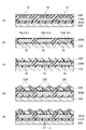
- FIG. 1 is a cross-sectional view showing an example of a semiconductor device manufactured by the method according to the embodiment of the present disclosure.
- 2 (a) to 2 (d) are diagrams showing a part of the method for manufacturing the semiconductor device shown in FIG. 1.
- 3 (a) to 3 (d) are views showing a method for manufacturing the semiconductor device shown in FIG. 1 and which is performed after the process of FIG. 2.
- 6 (a) to 6 (d) are diagrams showing a first method for manufacturing a semiconductor device, which is a step performed after the step of FIG. 7 (a) to 7 (d) are diagrams showing a first method for manufacturing a semiconductor device, which is a step performed after the step of FIG. 8 (a) to 8 (e) are views showing a part of a second method (face-up, with support plate) for manufacturing a semiconductor device.
- 6 (a) to 6 (e) are diagrams showing a second method for manufacturing a semiconductor device, which is a step performed after the step of FIG. 10 (a) to 10 (f) are diagrams showing a second method for manufacturing a semiconductor device, which is a step performed after the step of FIG. 9.
- FIG. 1 is a cross-sectional view schematically showing an example of a semiconductor device manufactured by the manufacturing method according to the present embodiment.
- the semiconductor device 1 is, for example, a device having a fan-out structure, and includes a semiconductor element 10, a sealing material layer 11, a protective layer 12, a rewiring layer 13, and a solder ball 14.
- the semiconductor device 1 is manufactured by, for example, a fan-out package (FO-PKG) technique, and may be manufactured by, for example, a fan-out wafer level package (FO-WLP) technique, or a fan-out panel level package ( It may be manufactured by FO-PLP) technique.
- FO-PKG fan-out package
- FO-WLP fan-out wafer level package
- FO-PLP fan-out panel level package
- the sealing material layer 11 is a layer in which the semiconductor element 10 is sealed with a sealing material such as resin.
- the protective layer 12 is a cured layer arranged on the second surface 10b of the semiconductor element 10 and the surface 11a of the encapsulant layer 11, and is formed by curing the curable adhesive layer 22 described later.
- the rewiring layer 13 is a layer for widening the terminal pitch of the connection terminal 10c on the first surface 10a side of the semiconductor element 10, and is composed of, for example, an insulating portion 13a such as polyimide and a wiring portion 13b such as copper wiring.
- the solder ball 14 is connected to a terminal whose terminal pitch is widened by the rewiring layer 13, whereby the connection terminal 10c of the semiconductor element 10 is pitch-converted (widened) and connected to the solder ball 14.
- FIGS. 2 to 4. are diagrams showing in order a method of manufacturing the semiconductor device 1.
- a plurality of semiconductor elements 10 each having a first surface 10a on which a connection terminal 10c is formed and a second surface 10b on the opposite side of the first surface 10a are prepared (FIG. 1 and FIG. 2 (b)).
- the plurality of semiconductor elements 10 are collectively formed by, for example, a normal semiconductor process, and then individualized by dicing to manufacture each semiconductor element 10. Since a conventional method can be used for this manufacturing process, the description thereof will be omitted.
- a curable adhesive layer 22 is formed on a carrier 20 having light transmittance such as a glass substrate, whereby a support member for supporting a plurality of semiconductor elements 10 is formed. 24 is formed (prepared).
- the thickness of the carrier 20 is set to, for example, 0.1 mm or more and 2.0 mm or less. There is. However, the thickness of the carrier 20 is not limited to this.
- the carrier 20 is preferably a glass substrate, but may be a transparent resin substrate having light transmittance. Further, the carrier 20 may have a disk-shaped wafer shape or a rectangular panel shape when viewed in a plan view.
- the curable adhesive layer 22 can be formed from, for example, a member (curable resin film) in which a resin composition which is a curable adhesive is formed into a film, and can be attached to the carrier 20 to form a support member 24. can do.
- the curable adhesive constituting the curable adhesive layer 22 is an adhesive that is cured by at least one of heat and light, and is, for example, a resin composition containing a thermoplastic resin and an epoxy curing agent.
- the thermoplastic resin contained in this curable adhesive may have a glass transition temperature of ⁇ 40 ° C. or higher and 40 ° C. or lower.
- Such a curable adhesive layer 22 may be preliminarily configured so that the thickness after curing is, for example, 1 ⁇ m or more and 400 ⁇ m or more.
- the curable resin film constituting the curable adhesive layer 22 may have a tack property at 25 ° C., more specifically, a tack property to the extent that it can be bonded to a glass substrate in an environment of 25 ° C. It may have sex.
- the adhesive force of the curable adhesive layer 22 to the carrier 20 is 1 MPa or more when the curable adhesive layer 22 is cured, and 5 MPa or less when the curable adhesive layer 22 is irradiated with a laser. It may be configured as follows.
- the curable adhesive layer 22 is a portion heated by laser irradiation in a laser peeling step (see FIG. 3D) described later, and the resin composition thereof contains a light absorber that absorbs laser light. It is preferable to have.
- the curable adhesive layer 22 is a curable resin film containing a light absorber, the curable adhesive layer 22 has sufficiently low light transmittance.
- the light absorber contained in the curable adhesive layer 22 a material that absorbs laser light from an excima laser and generates heat may be selected, and even if a black pigment or dye is added as the light absorber, for example. good.
- Specific examples of the light absorber include carbon black, aluminum, nickel, and titanium oxide.
- the content of the light absorber can be, for example, within the range in which the curable resin film constituting the curable adhesive layer 22 has a transmittance of 20% or less with respect to light having a wavelength of 351 nm.
- the content of the light absorber may be 1% by mass or more and 30% by mass or less, or 1% by mass or more and 20% by mass or less, based on the mass of the curable adhesive layer 22.
- the transmittance here means the ratio of the intensity of transmitted light to the intensity of incident light when light having a predetermined wavelength is incident on the curable adhesive layer 22 from one main surface side.
- the thermoplastic resin constituting the curable adhesive layer 22 may have a reactive group.
- the reactive group of the thermoplastic resin may be, for example, an epoxy group.
- the thermoplastic resin may be a (meth) acrylic copolymer or a (meth) acrylic copolymer having a reactive group.
- (meth) acrylic is used as a term to mean acrylic or methacrylic. Other similar terms are interpreted in the same way.
- the (meth) acrylic copolymer is a copolymer containing a (meth) acrylic monomer having a (meth) acryloyl group as a monomer unit.
- the (meth) acrylic copolymer forms a homopolymer having a glass transition temperature of 50 ° C. or higher, and a (meth) acrylic monomer forming a homopolymer having a glass transition temperature of 0 ° C. or lower.
- a copolymer containing a (meth) acrylic monomer having an epoxy group as a monomer unit may be used.
- the glass transition temperature of homopolymers formed by (meth) acrylic monomers with epoxy groups is not limited.
- the (meth) acrylic monomer forming a homopolymer having a glass transition temperature of 50 ° C. or higher and the (meth) acrylic monomer forming a homopolymer having a glass transition temperature of 0 ° C. or lower are monomers having no epoxy group. There can be.
- the weight average molecular weight of the thermoplastic resin constituting the curable adhesive layer 22 may be 200,000 or more and 1,000,000 or less.
- the weight average molecular weight here can be a standard polystyrene equivalent value measured by gel permeation chromatography.
- the content of the thermoplastic resin may be 10% by mass or more and 80% by mass or less based on the mass of the film constituting the curable adhesive layer 22.
- the curable resin film constituting the curable adhesive layer 22 may further contain a curable resin which is a compound having a reactive group.
- the curable resin may be an epoxy resin having two or more epoxy groups, and examples thereof include bisphenol A type epoxy resin, bisphenol F type epoxy resin, phenol novolac type epoxy resin, and cresol novolac type epoxy resin. Can be mentioned.
- the molecular weight of the curable resin may be 3000 or less.
- the curable adhesive layer 22 containing a curable resin has curability and tends to have an appropriate tack property.
- the content of the curable resin may be 1% by mass or more and 50% by mass or less based on the mass of the curable resin film constituting the curable adhesive layer 22.
- the curable adhesive layer 22 may further contain a silica filler.
- the content of the silica filler may be 1% by mass or more and 60% by mass or less, or 5% by mass or more and 60% by mass or less, based on the mass of the film constituting the curable adhesive layer 22.
- the curable adhesive layer 22 may further contain a curing agent that reacts with the reactive group of the thermoplastic resin, the reactive group of the curable resin, or both of them.
- the curing agent may be, for example, a phenol resin.
- the curable adhesive layer 22 may further contain a curing accelerator that accelerates the reaction of the curing agent.
- the curing accelerator may be an imidazole compound.
- the plurality of semiconductor elements 10 are arranged so that the second surfaces 10b of the plurality of semiconductor elements 10 face the curable adhesive layer 22.
- the step of attaching to the support member 24 is performed.
- the curable adhesive layer 22 is cured by at least one of heat and light, as shown in FIG. 2 (c).
- the cured layer 22a is used.
- the plurality of semiconductor elements 10 are fixed to the cured layer 22a of the support member 24a.
- the plurality of semiconductor elements 10 are sealed with a sealing resin (sealing material) such as epoxy.
- a sealing resin such as epoxy
- the semiconductor element 10 is entirely covered with the sealing resin and is included in the sealing material layer 26.
- the material for encapsulating the semiconductor element 10 may be an insulating resin other than epoxy.
- the sealing material is in a state where the plurality of semiconductor elements 10 are fixed to the support member 24a (carrier 20).
- a step of polishing the layer 26 is performed.
- the sealing material layer 26 is polished to the extent that the connection terminal 10c arranged on the first surface 10a side of the semiconductor element 10 is exposed to the outside from the sealing resin.
- the connection terminal 10c of the semiconductor element 10 is exposed from the surface of the polished encapsulant layer 26a, and connection is possible.
- the rewiring layer 28 is formed on the first surface 10a of the plurality of semiconductor elements 10.
- the rewiring layer 28 is a portion corresponding to the rewiring layer 13 of the semiconductor device 1 described above, and is composed of an insulating layer portion 28a such as polyimide and a wiring portion 28b such as copper wiring in the insulating layer portion 28a. ..
- the formation of the insulating layer and the formation of the wiring portion are repeated a predetermined number of times to form the wiring layer for performing the pitch conversion.
- the rewiring layer 28 is formed in a state where the semiconductor element 10 and the encapsulant layer 26a are stably arranged on the carrier 20, it becomes easy to construct a fine rewiring layer. ing.
- solder ball 30 is formed so that the connection terminal 10c of the semiconductor element 10 of the above is connected to the solder ball 30.
- the pitch of the solder balls 30 is formed to be wider than the terminal pitch of the connection terminal 10c of the semiconductor element 10.
- the solder ball 30 corresponds to the solder ball 14 in the semiconductor device 1 described above.
- the cured layer 22a is irradiated with laser light L from the carrier 20 side, laser marking is performed on the cured layer 22a, and necessary information such as a product name is written.
- the carrier 20 is removed from the cured layer 22a as shown in FIG. 3D.
- the laser used for removing the carrier 20 is, for example, an excimer laser which is a kind of UV laser, and the transmittance of the laser light of the carrier 20 made of a glass substrate is 99% or more.
- the light absorber in the cured layer 22a is generated to generate heat, and the cured layer 22a and the carrier 20 are separated from each other.
- the wavelength of the laser light emitted from the excimer laser to the cured layer 22a may be 532 nm, or may be another wavelength.
- the laser used here may be an excimer laser such as an XeF excimer laser (wavelength 351 nm), a XeCl excimer laser (wavelength 303 nm), a KrF excimer laser (wavelength 248 nm), or an ArF excimer laser (wavelength 193 nm).
- an excimer laser such as an XeF excimer laser (wavelength 351 nm), a XeCl excimer laser (wavelength 303 nm), a KrF excimer laser (wavelength 248 nm), or an ArF excimer laser (wavelength 193 nm).
- Other UV lasers such as a YAG laser (3rd harmonic wave) (wavelength 355 nm) and a YAG laser (4th harmonic wave) (wavelength 266 nm) may be used. The same applies to the lasers used below.
- the carrier removing method is not limited to this.
- the carrier 20 may be scraped off from the cured layer 22a, or the carrier 20 or the like may be dissolved (dissolved) with a predetermined solvent.
- the cured layer 22a may be removed together during this removal step.
- the exposed surface of the cured layer 22a or, when the cured layer 22a is removed, the exposed surface of the sealing material layer 26a with the encapsulant may be cleaned by a predetermined method.
- the carrier 20 is removed by such a method, the carrier 20 does not have to be a light-transmitting substrate, and the curable adhesive layer 22 does not have to contain a light absorber.
- the dicing tape 32 is attached to the exposed surface side of the cured layer 22a to form a wafer-shaped or panel-shaped die rearrangement body.
- the die rearrangement body is diced at a predetermined position S, and each portion including the semiconductor element 10 is individually separated to form a semiconductor device 1. do.
- the plurality of semiconductor devices 1 shown in FIGS. 4 (d) and 1 can be obtained from the die rearrangement body in which the plurality of semiconductor elements 10 are rearranged.
- 5 to 7 are views for sequentially explaining a first method (face-up, without support plate) for manufacturing a semiconductor device having a fan-out structure.
- 8 to 10 are views for sequentially explaining a second method (face-up, with support plate) for manufacturing a semiconductor device having a fan-out structure.
- the adhesive layer 122 is provided on the metal carrier 120.
- the adhesive layer 122 for example, a release sheet having an adhesive strength at room temperature but whose adhesive strength is reduced by heating is used.
- the plurality of semiconductor elements 10 are arranged on the adhesive layer 122 so that the second surface 10b of the plurality of semiconductor elements 10 faces the adhesive layer 122 (that is, face-up).
- the semiconductor element 10 is sealed with a sealing material to form the sealing material layer 124, and when the sealing is completed, the adhesive layer 122 or the like is heated to heat the semiconductor element 10.
- the adhesive layer 122 is peeled off from the surface to remove the carrier 120 (see FIG. 5D).
- the protective film 126 is attached to the surface of the encapsulant layer 124 on the side where the semiconductor element 10 is exposed.
- the protective film 126 is, for example, a film called a backside coat (BSC) or the like, and is a film that protects the semiconductor element 10 from contamination in a subsequent step.
- This protective film is made of, for example, an epoxy resin.
- the encapsulant layer 124 on the protective film 126 is polished until the connection terminal 10c of the semiconductor device 1 is exposed to obtain the encapsulant layer 124a.
- the rewiring layer 128 and the solder ball 130 are sequentially formed on the semiconductor element 10 arranged on the protective film 126.
- a protective tape 132 for protecting the solder balls 130 is further attached.
- the protective tape 132 is made of, for example, polyolefin.
- the protective film 126 is scraped off while the solder balls 130 are protected by the protective tape 132.
- a part of the semiconductor element 10 on the second surface 10b side may be scraped to reduce the thickness.
- the dicing tape 136 is attached via the BSC film 134, and the protective tape 132 is removed in that state.
- the BSC film 134 is made of, for example, an epoxy resin.
- each portion including the semiconductor element 10 is diced and individualized by the same method as that shown in FIGS. 4 (a) to 4 (d) to obtain each semiconductor device.
- the carrier 120 and the adhesive layer 122 are used in the step of processing the semiconductor element 10.
- the protective film 126 (See) and BSC film 134 (see FIG. 7B) are used.
- one kind of member including the carrier 20 and the curable adhesive layer 22 is used in many parts of the process, and is integrated into this one member. Therefore, according to the manufacturing method according to the present embodiment, the number of members used can be significantly reduced as compared with the first method, and the mounting process and the removing process of each member can be significantly reduced. The process of manufacturing the semiconductor device 1 can be greatly simplified.
- the semiconductor element 10 is arranged on the adhesive layer 122 and sealed with a sealing material. Therefore, the position shift of the semiconductor element 10 on the carrier 120 is likely to occur. Moreover, a heat-foaming film may be used as the adhesive layer 122, and in that case, the position of the semiconductor element 10 is more likely to shift.
- the semiconductor element 10 is arranged on the curable adhesive layer 22 and sealed with a sealing material. The curable adhesive layer 22 is cured to fix the semiconductor element 10 to the carrier 20 or the like before performing a treatment such as stopping. Therefore, according to the manufacturing method according to the present embodiment, it is possible to reliably prevent the positional deviation of the semiconductor element 10 as compared with the first method.
- the carrier 120 or the like may be a material having no heat resistance / chemical resistance, and the carrier 120 may be used at an early stage of the processing step.
- the encapsulant layer 124 is polished on the protective film 126 made of a relatively soft material. For this reason, the flatness of the die rearrangement body in which the plurality of semiconductor elements 10 are rearranged deteriorates, that is, the flatness of the encapsulant layer 124 or the semiconductor element 10 deteriorates, and the rewiring formed thereafter becomes poor. It becomes difficult to form the layer 128 finely.
- the method according to the present embodiment as shown in FIGS.
- the carrier 20 is made of a material having heat resistance / chemical resistance, so that the carrier 20 is continued. Polishing is performed with the encapsulant layer 26 arranged on the carrier 20. Therefore, according to the manufacturing method according to the present embodiment, the flatness of the encapsulant layer 26 and the semiconductor element 10 can be easily improved as compared with the first method, and the rewiring layer 28 to be formed thereafter is finely formed. can do.
- the back surface of the die rearrangement body in which the plurality of semiconductor elements 10 are arranged is made of epoxy. Since it is a resin, it may contaminate the process. Further, there is a possibility that the resin component of this epoxy may be eluted depending on the chemicals used in the process, and in this case, the yield of copper wiring or the like due to the plating process (wiring formation) in the rewiring layer may be affected.
- the carrier 20 continuously covers the back surface of the die rearrangement body during each step. The above-mentioned contamination or elution can be prevented. That is, the process of manufacturing the semiconductor device 1 can be maintained in a state of high cleanliness.
- the back surface of the die rearrangement body in which the semiconductor element 10 is rearranged is made of epoxy resin, which may contaminate the device environment and the like. Therefore, it is necessary to separately provide a case, a manufacturing apparatus, and a transport / suction mechanism used for manufacturing a fan-in wafer level package (WLP) whose back surface is silicon or the like.
- the carrier 20 made of glass or the like covers the back surface of the die rearrangement body during each step. Therefore, it is possible to prevent the above-mentioned contamination and the like.
- the manufacturing method according to the present embodiment it is possible to manufacture a semiconductor device having a fan-out structure such as FO-WLP by using the same manufacturing equipment as the fan-in WLP.
- a protective tape 132 is further used to protect the solder balls 130. is doing.
- the carrier 20 and the curable adhesive layer 22 are mainly used, and one member is used to aggregate the members used in each processing step. .. Therefore, according to the manufacturing method according to the present embodiment, the number of members used can be further reduced as compared with the first method, and the mounting process and the removing step of each member can be further reduced, and the semiconductor can be used. The process of manufacturing the device 1 can be further simplified.
- the carrier 120 is removed at an early stage, so that the die rearrangement body for rearranging the semiconductor element 10 is made too thin. It is difficult to reduce the height because each process cannot be performed.
- the carrier 20 and the curable adhesive layer 22 are mainly used, and each treatment step is performed using one member from the initial stage of the step. There is. Therefore, according to the manufacturing method according to the present embodiment, the die rearrangement body can be made thin from the beginning, and the height of the semiconductor device 1 can be further reduced.
- the second method according to the comparative example shown in FIGS. 8 to 10 and the comparison with the second method will be described.
- the curable release layer 222 is provided on the glass carrier 220.
- the curable release layer 222 is baked by heat or the like to obtain a cured layer 222a.
- a thermoplastic temporary fixing layer 224 is formed on the cured layer 222a, and the temporary fixed layer 224 is baked and cured by heat or the like to cure the cured layer. Let it be 224a.
- the plurality of semiconductor elements 10 are arranged on the cured layer 224a so that the second surface 10b of the plurality of semiconductor elements 10 faces the cured layer 224a (that is, face up). ..
- the cured layer 224a serving as the temporary fixing material is a thermoplastic resin, and the semiconductor element 10 is temporarily fixed at high temperature and high pressure.
- the semiconductor element 10 is sealed with a sealing material to form the sealing material layer 226.
- the sealing material layer 226 is polished until the connection terminal 10c of the semiconductor element 10 is exposed to obtain the sealing material layer 226a.
- connection terminal 10c may also be polished to make the connection terminal 10c a shorter connection terminal 10d.
- the rewiring layer 228 and the solder ball 230 are sequentially formed on the semiconductor element 10.
- the cured layer 222a is irradiated with laser light L from the carrier 220 side, the cured layer 222a is melted by heat, and the carrier 220 is peeled off.
- the cured layer 224a is exposed on the surface side.
- a protective tape 232 for protecting the solder ball 230 is further attached.
- the protective tape 232 is made of, for example, polyolefin.
- the cured layer 224a is removed by a predetermined cleaning process to expose the second surface 10b of the semiconductor element 10 to the outside.
- the second surface 10b side of the semiconductor element 10 may be polished to be thinned to form the semiconductor element 10A.
- the dicing tape 236 is attached via the BSC film 234, and the protective tape 232 is removed in that state.
- the BSC film 234 is made of, for example, an epoxy resin.
- laser marking is performed on the BSC film 234 with the laser beam L, and necessary information such as the product name is written.
- each portion including the semiconductor element 10 is diced and individualized by the same method as that shown in FIGS. 4 (a) to 4 (d) to obtain each semiconductor device.
- the curable release layer 222 (see FIGS. 8 (a) and 8 (b)) and the thermoplastic temporary fixing layer are used in the step of processing the semiconductor element 10.
- Three types of members are used: 224 (see FIGS. 8 (c) and 8 (d)) and protective tape 232 (see FIGS. 10 (b) and 10 (c)).
- one kind of member including the carrier 20 and the curable adhesive layer 22 is mainly used, and each treatment step is performed using this one member. Is aggregated. Therefore, according to the manufacturing method according to the present embodiment, the number of members used can be significantly reduced as compared with the second method, and the mounting process and the removing process of each member can be significantly reduced. The process of manufacturing the semiconductor device 1 can be greatly simplified.
- the cured layer 224a which is a temporary fixing material, is thermoplastic in the step shown in FIG. 8 (e)
- the cured layer 224a is pressed for a long time to attach the semiconductor element 10 to the carrier 220.
- the cycle time of the process of FIG. 8 (e) tends to be long.
- the semiconductor element 10 is arranged on the curable adhesive layer 22 and sealed with a sealing material.
- the curable adhesive layer 22 is cured to fix the semiconductor element 10 to the carrier 20 or the like before performing a treatment such as stopping. Therefore, according to the manufacturing method according to the present embodiment, the semiconductor element 10 can be fixed to the carrier 20 at a low temperature and a low pressure and in a short cycle time as compared with the second method.
- the curable release layer 222 is installed and baked, and the thermoplastic temporary fixing layer 224 is installed and baked to perform the semiconductor element. 10 is attached to the carrier 220. Therefore, since the semiconductor element 10 is attached to the carrier 220, the process becomes complicated and the number of members used increases.
- the semiconductor element 10 is arranged on the curable adhesive layer 22 to form a curable adhesive layer. 22 is cured to fix the semiconductor element 10 to the carrier 20 or the like. Therefore, according to the manufacturing method according to the present embodiment, the semiconductor element 10 can be easily connected by the carrier 20 as compared with the second method.
- a product in which the dicing tape 236 and the BSC film 234 are integrated after polishing may be used.
- This integrated product often does not have sufficient glue residue, dicing property, pick-up property, etc., and it is difficult to reduce the height of the semiconductor device 1.
- the curable adhesive layer 22 used for fixing the semiconductor element 10 to the carrier 20 at the beginning is used as it is in the semiconductor device 1, such an integrated product is used. There is no need and individual dicing tapes can be used. Therefore, it is possible to reduce the height of the semiconductor device by using a dicing tape suitable for reducing the height.
- the carrier 20 and the curable adhesive layer 22 are mainly used, and each treatment step is performed by using one member from the initial stage of the step. .. Therefore, according to the manufacturing method according to the present embodiment, the die rearrangement body can be made thin from the beginning, and the height of the semiconductor device 1 can be further reduced.
- the second method as shown in FIGS. 9 (e) and 10 (a), it is necessary to separate the cured layer 222a for peeling and the carrier 220 by a laser in the middle of the process, and the die is rearranged. It is necessary to clean and remove the cured layer 224a, which is an adhesive remaining on the body, with a solvent. Therefore, there is a problem that the process for removing the carrier 220 becomes complicated, and it takes time and effort accordingly.
- the manufacturing method according to the present embodiment as shown in FIG. 3D, the cured layer 22a is irradiated with a laser to remove the carrier 20, and most of the cured layer 22a is used as it is as a semiconductor device. It is a part of 1 (protective layer 12). Therefore, the removal work of the carrier 20 can be simplified.
- the process of manufacturing the semiconductor device 1 having a fan-out structure can be significantly simplified as compared with the first method and the second method according to the comparative example. Further, since the positional deviation of the semiconductor element 10 can be reduced, it becomes possible to manufacture the semiconductor device 1 having a smaller size and a lower profile with higher accuracy.
- the present invention is not limited to the above embodiments and can be applied to various embodiments.
- the method of manufacturing the semiconductor device 1 including the semiconductor device 10 has been described, but the semiconductor device or device including a plurality of electronic components in addition to or in place of the semiconductor device 10 with a plurality of electronic components.
- the present invention may be applied to the manufacturing method of.
- a plurality of electronic components are mounted on the support member 24 together with the plurality of semiconductor elements 10
- the fixing step shown in FIG. 2C the curable adhesive layer 22 is cured.
- a plurality of electronic components are fixed to the support member 24 together with the semiconductor element 10.
- the electronic component referred to here may be, for example, a passive element such as a cabasher or a resistor, or may be a component such as MEMS.
Abstract
This method for manufacturing a semiconductor device 1 comprises: a step for preparing a plurality of semiconductor elements 10, each having a first surface 10a on which a connection terminal 10c is formed and a second surface 10b on the reverse side from the first surface 10a; a step for preparing a support member 24 in which a curable adhesive layer 22 is formed on a carrier 20; a step for attaching the plurality of semiconductor elements 10 to the support member 24 such that the second surfaces 10b of the plurality of semiconductor elements 10 face the curable adhesive layer 22; a step for fixing the plurality of semiconductor elements 10 to the support member 24 by curing the curable adhesive layer 22; a step for sealing the plurality of semiconductor elements 10 with a sealing material; and a step for removing the carrier 20.
Description
本開示は、半導体装置の製造方法に関する。
This disclosure relates to a method for manufacturing a semiconductor device.
特許文献1には、半導体装置の製造に用いられる加熱剥離型粘着シートが開示されている。
Patent Document 1 discloses a heat-releaseable pressure-sensitive adhesive sheet used for manufacturing a semiconductor device.
半導体装置の製造方法の1つとして、ファンアウトパッケージが知られている。このファンアウトパッケージでは、個片化した半導体チップ(ダイ)を別のウエハ上に配列、封止して再配置ウエハとした後に、再配線層(RDL:Re-Distribution Layer)を形成し、各半導体装置を製造する。このようなファンアウトパッケージの工法では、例えば図5に示すように、半導体素子10をキャリア120上に再配置する際、キャリア120の粘着層122(例えば特許文献1を参照)上に半導体素子10をまずは配置することが行われている。しかしながら、粘着層122は半導体素子10を仮固定するものでありキャリア120上に半導体素子10を強固に固定するものではないため、封止材によって半導体素子を封止する際に半導体素子に位置ずれが生じることがある。
A fan-out package is known as one of the methods for manufacturing semiconductor devices. In this fan-out package, individualized semiconductor chips (dies) are arranged on another wafer, sealed to form a rearranged wafer, and then a rewiring layer (RDL: Re-Distribution Layer) is formed. Manufactures semiconductor devices. In such a fan-out package construction method, for example, as shown in FIG. 5, when the semiconductor element 10 is rearranged on the carrier 120, the semiconductor element 10 is placed on the adhesive layer 122 of the carrier 120 (see, for example, Patent Document 1). Is being placed first. However, since the adhesive layer 122 temporarily fixes the semiconductor element 10 and does not firmly fix the semiconductor element 10 on the carrier 120, the position shifts to the semiconductor element when the semiconductor element is sealed by the sealing material. May occur.
本開示は、半導体素子の位置ずれを低減するための製造方法を提供することを目的とする。
It is an object of the present disclosure to provide a manufacturing method for reducing the misalignment of a semiconductor element.
本開示は、一側面として、半導体装置の製造方法に関する。この半導体装置の製造方法は、接続端子が形成された第1面と該第1面の逆側にある第2面とをそれぞれが有する複数の半導体素子を準備する工程と、キャリア上に硬化性接着剤層が形成された支持部材を準備する工程と、複数の半導体素子の各第2面が硬化性接着剤層に向くように複数の半導体素子を支持部材に取り付ける工程と、硬化性接着剤層を硬化して複数の半導体素子を支持部材に固定する工程と、複数の半導体素子を封止材により封止する工程と、キャリアを除去する工程と、を備える。
This disclosure relates to a method for manufacturing a semiconductor device as one aspect. The method for manufacturing this semiconductor device includes a step of preparing a plurality of semiconductor devices each having a first surface on which a connection terminal is formed and a second surface on the opposite side of the first surface, and a curability on the carrier. A step of preparing a support member on which an adhesive layer is formed, a step of attaching a plurality of semiconductor elements to the support member so that each second surface of the plurality of semiconductor elements faces the curable adhesive layer, and a curable adhesive. It includes a step of curing a layer and fixing a plurality of semiconductor elements to a support member, a step of sealing the plurality of semiconductor elements with a sealing material, and a step of removing carriers.
この方法では、複数の半導体素子をキャリア上に取り付けるための層として硬化性接着剤層を用い、これを硬化して複数の半導体素子を支持部材に固定している。この場合、複数の半導体素子が硬化された硬化性接着剤層によりキャリア上に固定されるため、半導体素子の位置ずれを低減することができる。
In this method, a curable adhesive layer is used as a layer for mounting a plurality of semiconductor elements on a carrier, and the curable adhesive layer is cured to fix the plurality of semiconductor elements to a support member. In this case, since the plurality of semiconductor elements are fixed on the carrier by the cured curable adhesive layer, the misalignment of the semiconductor elements can be reduced.
上記製造方法において、キャリアがガラス基板であり、硬化性接着剤層のガラス基板への接着力は、硬化性接着剤層を硬化した場合に1MPa以上であり、且つ、硬化性接着剤層へレーザを照射した場合に5MPa以下であってもよい。硬化性接着剤層のガラス基板への接着力が、硬化性接着剤層を硬化した場合に1MPa以上であることにより、半導体素子の支持部材への固定をより強固にして、半導体素子の位置ずれをより低減することができる。また、硬化性接着剤層のガラス基板への接着力が、硬化性接着剤層へレーザを照射した場合に5MPa以下であることにより、キャリアを除去する際にレーザ照射で簡単に取り外すことが可能となり、作業効率を改善することができる。
In the above manufacturing method, the carrier is a glass substrate, the adhesive force of the curable adhesive layer to the glass substrate is 1 MPa or more when the curable adhesive layer is cured, and the laser is applied to the curable adhesive layer. It may be 5 MPa or less when irradiated with. When the adhesive force of the curable adhesive layer to the glass substrate is 1 MPa or more when the curable adhesive layer is cured, the fixing of the semiconductor element to the support member is further strengthened, and the position of the semiconductor element is displaced. Can be further reduced. Further, since the adhesive force of the curable adhesive layer to the glass substrate is 5 MPa or less when the curable adhesive layer is irradiated with a laser, it can be easily removed by laser irradiation when removing the carrier. Therefore, work efficiency can be improved.
上記製造方法において、硬化性接着剤層は、熱可塑性樹脂、及びエポキシ硬化剤を含む樹脂組成物から形成され、熱可塑性樹脂のガラス転移温度が-40℃以上40℃以下であってもよい。この場合、パッケージ完成後の反りを低減するといったことが可能となる。なお、硬化性接着剤層は、光吸収剤を含んでもよく、又は、光吸収特性を有していてもよい。光吸収剤又は光吸収特性は、例えばUVレーザの一種であるエキシマレーザの波長域である193nm以上351nm以下の光を吸収してもよい。このエキシマレーザとしては、例えば、XeFエキシマレーザ(波長351nm)、XeClエキシマレーザ(波長303nm)、KrFエキシマレーザ(波長248nm)、ArFエキシマレーザ(波長193nm)等を挙げることができる。また、その他のUVレーザである、YAGレーザ(3倍波)(波長355nm)、YAGレーザ(4倍波)(波長266nm)等を用いてもよい。
In the above production method, the curable adhesive layer is formed from a resin composition containing a thermoplastic resin and an epoxy curing agent, and the glass transition temperature of the thermoplastic resin may be −40 ° C. or higher and 40 ° C. or lower. In this case, it is possible to reduce the warp after the package is completed. The curable adhesive layer may contain a light absorber or may have light absorption characteristics. The light absorber or the light absorption characteristic may absorb light of 193 nm or more and 351 nm or less, which is the wavelength range of an excimer laser, which is a kind of UV laser, for example. Examples of the excimer laser include a XeF excimer laser (wavelength 351 nm), a XeCl excimer laser (wavelength 303 nm), a KrF excimer laser (wavelength 248 nm), an ArF excimer laser (wavelength 193 nm), and the like. Further, other UV lasers such as a YAG laser (3rd harmonic wave) (wavelength 355 nm) and a YAG laser (4th harmonic wave) (wavelength 266 nm) may be used.
上記製造方法において、硬化性接着剤層の厚みは、硬化後において1μm以上400μm以下であってもよい。この場合、硬化した硬化性接着剤層により複数の半導体素子をより確実に保持して、半導体素子の位置ずれを一層低減することができる。また、厚みが400μm以下であることにより、製造される半導体装置の低背化を図ることが可能である。
In the above manufacturing method, the thickness of the curable adhesive layer may be 1 μm or more and 400 μm or less after curing. In this case, the cured curable adhesive layer can more reliably hold the plurality of semiconductor elements, and the misalignment of the semiconductor elements can be further reduced. Further, when the thickness is 400 μm or less, it is possible to reduce the height of the manufactured semiconductor device.
上記製造方法において、キャリアは、ガラス基板又は透明樹脂基板であり、その厚さが0.1mm以上2.0mm以下であることが好ましい。この場合、キャリアによって保持される複数の半導体素子等の位置ずれを抑制した状態で、例えば、封止材の研磨又は再配線層の形成などの工程を行うことができ、より低背化した精度のよい半導体装置を作製することが可能となる。
In the above manufacturing method, the carrier is preferably a glass substrate or a transparent resin substrate, and the thickness thereof is preferably 0.1 mm or more and 2.0 mm or less. In this case, it is possible to perform steps such as polishing the encapsulant or forming a rewiring layer while suppressing the displacement of the plurality of semiconductor elements held by the carriers, and the accuracy is further reduced. It is possible to manufacture a good semiconductor device.
上記製造方法において、複数の半導体素子が支持部材に固定された状態で、支持部材に固定された複数の半導体素子を封止する封止材層を研磨する工程を更に備えてもよい。この場合、従来のファンアウト工法で用いている半導体素子の保護膜を別途設ける必要がなく、当初から硬化性接着剤層によって貼り付けられているキャリアをそのまま各工程における保護膜として用いることができる。これにより、別途、保護膜を用いる場合に比べて、製造工程を簡素化したり、また製造コストを低減したりすることができる。また、当初からのキャリアをそのまま利用しているため、途中で別途、保護膜を貼り付ける場合に比べて、複数の半導体素子の位置ずれをより一層低減することも可能である。
In the above manufacturing method, a step of polishing a sealing material layer for sealing a plurality of semiconductor elements fixed to the support member may be further provided in a state where the plurality of semiconductor elements are fixed to the support member. In this case, it is not necessary to separately provide a protective film for the semiconductor element used in the conventional fan-out method, and the carrier attached by the curable adhesive layer from the beginning can be used as it is as the protective film in each process. .. As a result, the manufacturing process can be simplified and the manufacturing cost can be reduced as compared with the case where the protective film is separately used. Further, since the carrier from the beginning is used as it is, it is possible to further reduce the misalignment of a plurality of semiconductor elements as compared with the case where a protective film is separately attached on the way.
上記製造方法において、複数の半導体素子が支持部材に固定された状態で、支持部材に固定された複数の半導体素子の第1面上に再配線層を形成する工程を更に備えてもよい。従来のファンアウト工法では、半導体素子を粘着層でキャリアに取り付けていたり、剛性のあるキャリアを途中で取り外して封止材を研磨していたりするため、封止材及び封止材に封止されている半導体素子の表面の平坦性が悪くなり、微細な再配線層を形成することが困難であった。これに対し、本製造方法によれば、キャリア上に複数の半導体素子を取り付けたまま封止材で封止等されるため、封止材及び封止材に封止されている半導体素子の表面の平坦性を高めることができる。このため、本製造方法によれば、微細な再配線層を容易に形成することが可能となる。
In the above manufacturing method, a step of forming a rewiring layer on the first surface of the plurality of semiconductor elements fixed to the support member may be further provided in a state where the plurality of semiconductor elements are fixed to the support member. In the conventional fan-out method, the semiconductor element is attached to the carrier with an adhesive layer, or the rigid carrier is removed in the middle and the encapsulant is polished, so that the encapsulant and the encapsulant are sealed. The flatness of the surface of the semiconductor device is deteriorated, and it is difficult to form a fine rewiring layer. On the other hand, according to this manufacturing method, since a plurality of semiconductor elements are sealed with a sealing material while being mounted on the carrier, the surface of the sealing material and the semiconductor element sealed by the sealing material is sealed. The flatness of the can be improved. Therefore, according to this manufacturing method, it is possible to easily form a fine rewiring layer.
上記製造方法において、複数の半導体素子が支持部材に固定された状態で、複数の半導体素子の接続端子又は再配線層に半田ボールを取り付ける工程を更に備えてもよい。この場合、キャリア上に位置ずれなく取り付けられた半導体素子又は再配線層に対して半田ボールを取り付けるため、精度よく半田ボールを取り付けることが可能となる。
In the above manufacturing method, a step of attaching a solder ball to the connection terminal or the rewiring layer of the plurality of semiconductor elements in a state where the plurality of semiconductor elements are fixed to the support member may be further provided. In this case, since the solder balls are attached to the semiconductor element or the rewiring layer mounted on the carrier without any positional deviation, the solder balls can be attached with high accuracy.
上記製造方法において、キャリアが光透過性基板であり、硬化性接着剤層が光吸収剤を含み、除去する工程では、硬化した硬化性接着剤層に対してキャリア側からレーザ光を照射して、キャリアを除去することが好ましい。この場合、キャリアの取り外し作業を簡易なものとすることができる。また、レーザ光による処理のため、キャリアを取り外した表面の平坦性又は清浄度を高くすることも可能である。
In the above manufacturing method, the carrier is a light-transmitting substrate, the curable adhesive layer contains a light absorber, and in the step of removing the carrier, the cured curable adhesive layer is irradiated with laser light from the carrier side. , It is preferable to remove the carrier. In this case, the carrier removal work can be simplified. Further, it is possible to improve the flatness or cleanliness of the surface from which the carrier has been removed because of the treatment by the laser beam.
上記製造方法において、除去する工程では、キャリアを削る又は溶かすことにより、キャリアを除去してもよい。
In the above manufacturing method, the carrier may be removed by scraping or melting the carrier in the removing step.
上記製造方法において、除去する工程の後に、硬化した硬化性接着剤層又は封止材による封止材層の何れかの露出面をクリーニングする工程を更に備えてもよい。この場合、製造される半導体装置の表面をより綺麗にして見栄えをよくすることができる。
In the above manufacturing method, after the removing step, a step of cleaning the exposed surface of either the cured curable adhesive layer or the sealing material layer with the sealing material may be further provided. In this case, the surface of the manufactured semiconductor device can be made cleaner and the appearance can be improved.
上記製造方法において、除去する工程の後に複数の半導体素子を個片化する工程を更に備えてもよい。この場合、半導体素子を含む各半導体装置へ個片化するまでキャリア上に保持して各種の工程を行うことになるため、従来用いていた各種の保護層(バックサイドコート等)を用いなくてもよくなり、製造工程の削減又は製造コストの低減を図ることができる。
In the above manufacturing method, a step of separating a plurality of semiconductor elements into individual pieces may be further provided after the step of removing. In this case, since various processes are performed by holding the semiconductor device on the carrier until it is individualized into each semiconductor device including the semiconductor element, it is not necessary to use various protective layers (backside coat, etc.) conventionally used. It also improves, and it is possible to reduce the manufacturing process or the manufacturing cost.
上記製造方法において、取り付ける工程では、複数の半導体素子と共に複数の電子部品を支持部材に取り付け、固定する工程では、硬化性接着剤層を硬化して複数の電子部品を支持部材に固定してもよい。この場合、電子部品も位置精度よく取り付けることが可能となり、より複雑な半導体装置を簡易な方法で作製することが可能となる。
In the above manufacturing method, in the mounting step, a plurality of electronic components are attached to the support member together with the plurality of semiconductor elements, and in the step of fixing, the curable adhesive layer may be cured and the plurality of electronic components may be fixed to the support member. good. In this case, electronic components can also be mounted with high positional accuracy, and a more complicated semiconductor device can be manufactured by a simple method.
本開示の一側面によれば、半導体装置の製造にあたり、半導体素子の位置ずれを低減することができる。
According to one aspect of the present disclosure, it is possible to reduce the misalignment of the semiconductor element in the manufacture of the semiconductor device.
以下、必要により図面を参照しながら本開示のいくつかの実施形態について詳細に説明する。ただし、本開示は以下の実施形態に限られるものではない。以下の説明では、同一又は相当部分には同一の符号を付し、重複する説明は省略することがある。上下左右等の位置関係は、特に断らない限り、図面に示す位置関係に基づくものとする。図面の寸法比率は図示の比率に限られるものではない。
Hereinafter, some embodiments of the present disclosure will be described in detail with reference to the drawings as necessary. However, the present disclosure is not limited to the following embodiments. In the following description, the same or corresponding parts may be designated by the same reference numerals, and duplicate description may be omitted. Unless otherwise specified, the positional relationship such as up, down, left, and right shall be based on the positional relationship shown in the drawings. The dimensional ratios in the drawings are not limited to the ratios shown.
(半導体装置の構成)
図1は、本実施形態に係る製造方法によって製造される半導体装置の一例を模式的に示す断面図である。図1に示すように、半導体装置1は、例えばファンアウト構造を有する装置であり、半導体素子10、封止材層11、保護層12、再配線層13、及び、半田ボール14を備える。半導体装置1は、例えばファンアウトパッケージ(FO-PKG)技術によって作製されるものであり、例えばファンアウトウエハレベルパッケージ(FO-WLP)技術によって作製されてもよく、又は、ファンアウトパネルレベルパッケージ(FO-PLP)技術によって作製されてもよい。封止材層11は、半導体素子10を樹脂等の封止材により封止した層である。保護層12は、半導体素子10の第2面10b及び封止材層11の面11a上に配置された硬化層であり、後述する硬化性接着剤層22を硬化することにより形成される。再配線層13は、半導体素子10の第1面10a側の接続端子10cの端子ピッチを広げるための層であり、例えばポリイミド等の絶縁部分13a及び銅配線等の配線部分13bから構成される。半田ボール14は、再配線層13によって端子ピッチが広げられた端子に接続され、これにより半導体素子10の接続端子10cがピッチ変換されて(広げられて)半田ボール14に接続される。 (Semiconductor device configuration)
FIG. 1 is a cross-sectional view schematically showing an example of a semiconductor device manufactured by the manufacturing method according to the present embodiment. As shown in FIG. 1, thesemiconductor device 1 is, for example, a device having a fan-out structure, and includes a semiconductor element 10, a sealing material layer 11, a protective layer 12, a rewiring layer 13, and a solder ball 14. The semiconductor device 1 is manufactured by, for example, a fan-out package (FO-PKG) technique, and may be manufactured by, for example, a fan-out wafer level package (FO-WLP) technique, or a fan-out panel level package ( It may be manufactured by FO-PLP) technique. The sealing material layer 11 is a layer in which the semiconductor element 10 is sealed with a sealing material such as resin. The protective layer 12 is a cured layer arranged on the second surface 10b of the semiconductor element 10 and the surface 11a of the encapsulant layer 11, and is formed by curing the curable adhesive layer 22 described later. The rewiring layer 13 is a layer for widening the terminal pitch of the connection terminal 10c on the first surface 10a side of the semiconductor element 10, and is composed of, for example, an insulating portion 13a such as polyimide and a wiring portion 13b such as copper wiring. The solder ball 14 is connected to a terminal whose terminal pitch is widened by the rewiring layer 13, whereby the connection terminal 10c of the semiconductor element 10 is pitch-converted (widened) and connected to the solder ball 14.
図1は、本実施形態に係る製造方法によって製造される半導体装置の一例を模式的に示す断面図である。図1に示すように、半導体装置1は、例えばファンアウト構造を有する装置であり、半導体素子10、封止材層11、保護層12、再配線層13、及び、半田ボール14を備える。半導体装置1は、例えばファンアウトパッケージ(FO-PKG)技術によって作製されるものであり、例えばファンアウトウエハレベルパッケージ(FO-WLP)技術によって作製されてもよく、又は、ファンアウトパネルレベルパッケージ(FO-PLP)技術によって作製されてもよい。封止材層11は、半導体素子10を樹脂等の封止材により封止した層である。保護層12は、半導体素子10の第2面10b及び封止材層11の面11a上に配置された硬化層であり、後述する硬化性接着剤層22を硬化することにより形成される。再配線層13は、半導体素子10の第1面10a側の接続端子10cの端子ピッチを広げるための層であり、例えばポリイミド等の絶縁部分13a及び銅配線等の配線部分13bから構成される。半田ボール14は、再配線層13によって端子ピッチが広げられた端子に接続され、これにより半導体素子10の接続端子10cがピッチ変換されて(広げられて)半田ボール14に接続される。 (Semiconductor device configuration)
FIG. 1 is a cross-sectional view schematically showing an example of a semiconductor device manufactured by the manufacturing method according to the present embodiment. As shown in FIG. 1, the
(半導体装置の製造方法)
次に、図2~図4を参照して、半導体装置1を製造する方法について説明する。図2~図4は、半導体装置1を製造する方法を順に示す図である。この半導体装置の製造方法では、まず、接続端子10cが形成された第1面10aと第1面10aの逆側にある第2面10bとをそれぞれが有する複数の半導体素子10を準備する(図1及び図2(b)を参照)。複数の半導体素子10は、例えば、通常の半導体プロセスによってまとめて形成され、その後、ダイシングによって個片化され、各半導体素子10が作製される。この作製工程は、従来の工法を用いることができるため、説明を省略する。 (Manufacturing method of semiconductor device)
Next, a method for manufacturing thesemiconductor device 1 will be described with reference to FIGS. 2 to 4. 2 to 4 are diagrams showing in order a method of manufacturing the semiconductor device 1. In the method for manufacturing this semiconductor device, first, a plurality of semiconductor elements 10 each having a first surface 10a on which a connection terminal 10c is formed and a second surface 10b on the opposite side of the first surface 10a are prepared (FIG. 1 and FIG. 2 (b)). The plurality of semiconductor elements 10 are collectively formed by, for example, a normal semiconductor process, and then individualized by dicing to manufacture each semiconductor element 10. Since a conventional method can be used for this manufacturing process, the description thereof will be omitted.
次に、図2~図4を参照して、半導体装置1を製造する方法について説明する。図2~図4は、半導体装置1を製造する方法を順に示す図である。この半導体装置の製造方法では、まず、接続端子10cが形成された第1面10aと第1面10aの逆側にある第2面10bとをそれぞれが有する複数の半導体素子10を準備する(図1及び図2(b)を参照)。複数の半導体素子10は、例えば、通常の半導体プロセスによってまとめて形成され、その後、ダイシングによって個片化され、各半導体素子10が作製される。この作製工程は、従来の工法を用いることができるため、説明を省略する。 (Manufacturing method of semiconductor device)
Next, a method for manufacturing the
また、図2(a)に示すように、ガラス基板等の光透過性を有するキャリア20上に硬化性接着剤層22を形成し、これにより、複数の半導体素子10を支持するための支持部材24を形成(準備)する。本製造方法では、ダイ再配置体上に取り付けられた半導体素子10を再度個片化するまでキャリア20上で各種の工程を行うため、キャリア20の厚みを例えば0.1mm以上2.0mm以下としている。但し、キャリア20の厚みはこれに限定されない。キャリア20は、ガラス基板であることが好ましいが、光透過性を有する透明樹脂基板であってもよい。また、キャリア20は、平面視した際に円板状のウエハ形状であってもよいし、矩形状のパネル形状であってもよい。
Further, as shown in FIG. 2A, a curable adhesive layer 22 is formed on a carrier 20 having light transmittance such as a glass substrate, whereby a support member for supporting a plurality of semiconductor elements 10 is formed. 24 is formed (prepared). In this manufacturing method, various steps are performed on the carrier 20 until the semiconductor element 10 mounted on the die rearrangement body is re-fragmented. Therefore, the thickness of the carrier 20 is set to, for example, 0.1 mm or more and 2.0 mm or less. There is. However, the thickness of the carrier 20 is not limited to this. The carrier 20 is preferably a glass substrate, but may be a transparent resin substrate having light transmittance. Further, the carrier 20 may have a disk-shaped wafer shape or a rectangular panel shape when viewed in a plan view.
硬化性接着剤層22は、例えば、硬化性接着剤である樹脂組成物をフィルム状にした部材(硬化性樹脂フィルム)から形成することができ、キャリア20に貼り付けることにより、支持部材24とすることができる。硬化性接着剤層22を構成する硬化性接着剤は、熱及び光の少なくとも一方によって硬化する接着剤であり、例えば、熱可塑性樹脂、及び、エポキシ硬化剤を含む樹脂組成物である。この硬化性接着剤に含まれる熱可塑性樹脂は、そのガラス転移温度が-40℃以上40℃以下であってもよい。このような硬化性接着剤層22は、硬化後の厚みが例えば1μm以上400μm以上になるように予め構成されていてもよい。また、硬化性接着剤層22を構成する硬化性樹脂フィルムは、25℃においてタック性を有してもよく、より具体的には、25℃の環境下でガラス基板に貼り合わせられる程度のタック性を有していてもよい。硬化性接着剤層22のキャリア20への接着力は、硬化性接着剤層22を硬化した場合に1MPa以上であり、且つ、硬化性接着剤層22へレーザを照射した場合に5MPa以下となるように構成されていてもよい。
The curable adhesive layer 22 can be formed from, for example, a member (curable resin film) in which a resin composition which is a curable adhesive is formed into a film, and can be attached to the carrier 20 to form a support member 24. can do. The curable adhesive constituting the curable adhesive layer 22 is an adhesive that is cured by at least one of heat and light, and is, for example, a resin composition containing a thermoplastic resin and an epoxy curing agent. The thermoplastic resin contained in this curable adhesive may have a glass transition temperature of −40 ° C. or higher and 40 ° C. or lower. Such a curable adhesive layer 22 may be preliminarily configured so that the thickness after curing is, for example, 1 μm or more and 400 μm or more. Further, the curable resin film constituting the curable adhesive layer 22 may have a tack property at 25 ° C., more specifically, a tack property to the extent that it can be bonded to a glass substrate in an environment of 25 ° C. It may have sex. The adhesive force of the curable adhesive layer 22 to the carrier 20 is 1 MPa or more when the curable adhesive layer 22 is cured, and 5 MPa or less when the curable adhesive layer 22 is irradiated with a laser. It may be configured as follows.
硬化性接着剤層22は、後述するレーザ剥離工程(図3(d)を参照)でレーザ照射により加熱される部分であり、その樹脂組成物は、レーザ光を吸収する光吸収剤を含んでいることが好ましい。硬化性接着剤層22が光吸収剤を含む硬化性樹脂フィルムである場合、硬化性接着剤層22は十分に低い光透過性となる。硬化性接着剤層22に含まれる光吸収剤として、エキシマレーザによるレーザ光を吸収して発熱する材料が選定されてもよく、例えば黒色の顔料又は染料などが光吸収剤として添加されていてもよい。光吸収剤の具体例としては、カーボンブラック、アルミニウム、ニッケル、酸化チタンが挙げられる。光吸収剤の含有量は、例えば硬化性接着剤層22を構成する硬化性樹脂フィルムが波長351nmの光に対する透過率が20%以下となる範囲内のものとすることができる。具体的には、光吸収剤の含有量が、硬化性接着剤層22の質量を基準として1質量%以上30質量%以下、又は1質量%以上20質量%以下であってもよい。ここでの透過率は、硬化性接着剤層22に対して一方の主面側から所定の波長を有する光を入射させたときに、入射光の強度に対する透過光の強度の割合を意味する。
The curable adhesive layer 22 is a portion heated by laser irradiation in a laser peeling step (see FIG. 3D) described later, and the resin composition thereof contains a light absorber that absorbs laser light. It is preferable to have. When the curable adhesive layer 22 is a curable resin film containing a light absorber, the curable adhesive layer 22 has sufficiently low light transmittance. As the light absorber contained in the curable adhesive layer 22, a material that absorbs laser light from an excima laser and generates heat may be selected, and even if a black pigment or dye is added as the light absorber, for example. good. Specific examples of the light absorber include carbon black, aluminum, nickel, and titanium oxide. The content of the light absorber can be, for example, within the range in which the curable resin film constituting the curable adhesive layer 22 has a transmittance of 20% or less with respect to light having a wavelength of 351 nm. Specifically, the content of the light absorber may be 1% by mass or more and 30% by mass or less, or 1% by mass or more and 20% by mass or less, based on the mass of the curable adhesive layer 22. The transmittance here means the ratio of the intensity of transmitted light to the intensity of incident light when light having a predetermined wavelength is incident on the curable adhesive layer 22 from one main surface side.
硬化性接着剤層22を構成する熱可塑性樹脂は、反応性基を有していてもよい。熱可塑性樹脂の反応性基は、例えばエポキシ基であってもよい。熱可塑性樹脂は、(メタ)アクリル共重合体であってもよく、反応性基を有する(メタ)アクリル共重合体であってもよい。本明細書において、「(メタ)アクリル」は、アクリル又はメタクリルを意味する用語として用いられる。他の類似の用語も同様に解釈される。
The thermoplastic resin constituting the curable adhesive layer 22 may have a reactive group. The reactive group of the thermoplastic resin may be, for example, an epoxy group. The thermoplastic resin may be a (meth) acrylic copolymer or a (meth) acrylic copolymer having a reactive group. As used herein, "(meth) acrylic" is used as a term to mean acrylic or methacrylic. Other similar terms are interpreted in the same way.
(メタ)アクリル共重合体は、(メタ)アクリロイル基を有する(メタ)アクリルモノマーをモノマー単位として含む共重合体である。(メタ)アクリル共重合体が、50℃以上のガラス転移温度を有するホモポリマーを形成する(メタ)アクリルモノマーと、0℃以下のガラス転移温度を有するホモポリマーを形成する(メタ)アクリルモノマーと、エポキシ基を有する(メタ)アクリルモノマーとをモノマー単位として含む共重合体であってもよい。エポキシ基を有する(メタ)アクリルモノマーによって形成されるホモポリマーのガラス転移温度は制限されない。50℃以上のガラス転移温度を有するホモポリマーを形成する(メタ)アクリルモノマー、及び、0℃以下のガラス転移温度を有するホモポリマーを形成する(メタ)アクリルモノマーは、エポキシ基を有しないモノマーであることができる。
The (meth) acrylic copolymer is a copolymer containing a (meth) acrylic monomer having a (meth) acryloyl group as a monomer unit. The (meth) acrylic copolymer forms a homopolymer having a glass transition temperature of 50 ° C. or higher, and a (meth) acrylic monomer forming a homopolymer having a glass transition temperature of 0 ° C. or lower. , A copolymer containing a (meth) acrylic monomer having an epoxy group as a monomer unit may be used. The glass transition temperature of homopolymers formed by (meth) acrylic monomers with epoxy groups is not limited. The (meth) acrylic monomer forming a homopolymer having a glass transition temperature of 50 ° C. or higher and the (meth) acrylic monomer forming a homopolymer having a glass transition temperature of 0 ° C. or lower are monomers having no epoxy group. There can be.
硬化性接着剤層22を構成する熱可塑性樹脂の重量平均分子量は、200,000以上1,000,000以下であってもよい。ここでの重量平均分子量は、ゲル浸透クロマトグラフィーによって測定される、標準ポリスチレン換算値であることができる。また、熱可塑性樹脂の含有量は、硬化性接着剤層22を構成するフィルムの質量を基準として、10質量%以上80質量%以下であってもよい。
The weight average molecular weight of the thermoplastic resin constituting the curable adhesive layer 22 may be 200,000 or more and 1,000,000 or less. The weight average molecular weight here can be a standard polystyrene equivalent value measured by gel permeation chromatography. Further, the content of the thermoplastic resin may be 10% by mass or more and 80% by mass or less based on the mass of the film constituting the curable adhesive layer 22.
硬化性接着剤層22を構成する硬化性樹脂フィルムは、反応性基を有する化合物である硬化性樹脂を更に含んでいてもよい。硬化性樹脂は、2以上のエポキシ基を有するエポキシ樹脂であってもよく、その例としては、ビスフェノールA型エポキシ樹脂、ビスフェノールF型エポキシ樹脂、フェノールノボラック型エポキシ樹脂、及びクレゾールノボラック型エポキシ樹脂が挙げられる。硬化性樹脂の分子量は3000以下であってもよい。硬化性樹脂を含む硬化性接着剤層22は、硬化性を有するとともに、適度なタック性を有し易い。硬化性樹脂の含有量は、硬化性接着剤層22を構成する硬化性樹脂フィルムの質量を基準として、1質量%以上50質量%以下であってもよい。
The curable resin film constituting the curable adhesive layer 22 may further contain a curable resin which is a compound having a reactive group. The curable resin may be an epoxy resin having two or more epoxy groups, and examples thereof include bisphenol A type epoxy resin, bisphenol F type epoxy resin, phenol novolac type epoxy resin, and cresol novolac type epoxy resin. Can be mentioned. The molecular weight of the curable resin may be 3000 or less. The curable adhesive layer 22 containing a curable resin has curability and tends to have an appropriate tack property. The content of the curable resin may be 1% by mass or more and 50% by mass or less based on the mass of the curable resin film constituting the curable adhesive layer 22.
硬化性接着剤層22は、シリカフィラーを更に含んでいてもよい。シリカフィラーの含有量は、硬化性接着剤層22を構成するフィルムの質量を基準として、1質量%以上60質量%以下、又は5質量%以上60質量%以下であってもよい。
The curable adhesive layer 22 may further contain a silica filler. The content of the silica filler may be 1% by mass or more and 60% by mass or less, or 5% by mass or more and 60% by mass or less, based on the mass of the film constituting the curable adhesive layer 22.
硬化性接着剤層22は、熱可塑性樹脂の反応性基、硬化性樹脂の反応性基、又はこれらの両方と反応する硬化剤を更に含んでいてもよい。硬化剤は、例えばフェノール樹脂であってもよい。硬化性接着剤層22が硬化剤を含む場合、硬化剤の反応を促進する硬化促進剤を更に含んでいてもよい。例えば硬化剤がフェノール樹脂である場合、硬化促進剤がイミダゾール化合物であってもよい。
The curable adhesive layer 22 may further contain a curing agent that reacts with the reactive group of the thermoplastic resin, the reactive group of the curable resin, or both of them. The curing agent may be, for example, a phenol resin. When the curable adhesive layer 22 contains a curing agent, it may further contain a curing accelerator that accelerates the reaction of the curing agent. For example, when the curing agent is a phenol resin, the curing accelerator may be an imidazole compound.
続いて、支持部材24の準備が終了すると、図2(b)に示すように、複数の半導体素子10の各第2面10bが硬化性接着剤層22に向くように複数の半導体素子10を支持部材24に取り付ける工程を行う。
Subsequently, when the preparation of the support member 24 is completed, as shown in FIG. 2B, the plurality of semiconductor elements 10 are arranged so that the second surfaces 10b of the plurality of semiconductor elements 10 face the curable adhesive layer 22. The step of attaching to the support member 24 is performed.
続いて、支持部材24の硬化性接着剤層22上に半導体素子10が取り付けられると、図2(c)に示すように、硬化性接着剤層22を熱及び光の少なくとも一方によって硬化させて硬化層22aとする。この硬化により、複数の半導体素子10は、支持部材24aの硬化層22aに固定される。
Subsequently, when the semiconductor element 10 is mounted on the curable adhesive layer 22 of the support member 24, the curable adhesive layer 22 is cured by at least one of heat and light, as shown in FIG. 2 (c). The cured layer 22a is used. By this curing, the plurality of semiconductor elements 10 are fixed to the cured layer 22a of the support member 24a.
続いて、半導体素子10が支持部材24aに固定されると、図2(d)に示すように、エポキシ等の封止樹脂(封止材)により、複数の半導体素子10を封止する。これにより、半導体素子10はその全体が封止樹脂に覆われて封止材層26内に包含される。この際、複数の半導体素子10は支持部材24aに固定されているため、各半導体素子10のキャリア20(支持部材24a)に対する位置ずれは生じない。半導体素子10を封止する材料は、エポキシ以外の絶縁樹脂であってもよい。
Subsequently, when the semiconductor element 10 is fixed to the support member 24a, as shown in FIG. 2D, the plurality of semiconductor elements 10 are sealed with a sealing resin (sealing material) such as epoxy. As a result, the semiconductor element 10 is entirely covered with the sealing resin and is included in the sealing material layer 26. At this time, since the plurality of semiconductor elements 10 are fixed to the support member 24a, the positional deviation of each semiconductor element 10 with respect to the carrier 20 (support member 24a) does not occur. The material for encapsulating the semiconductor element 10 may be an insulating resin other than epoxy.
続いて、半導体素子10が封止樹脂により封止されると、図3(a)に示すように、複数の半導体素子10が支持部材24a(キャリア20)に固定された状態で、封止材層26を研磨する工程を行う。この研磨工程では、例えば、半導体素子10の第1面10a側に配置されている接続端子10cが封止樹脂から外側に露出する程度まで封止材層26を研磨する。これにより、研磨済の封止材層26aの表面から半導体素子10の接続端子10cが露出して、接続可能となる。
Subsequently, when the semiconductor element 10 is sealed with the sealing resin, as shown in FIG. 3A, the sealing material is in a state where the plurality of semiconductor elements 10 are fixed to the support member 24a (carrier 20). A step of polishing the layer 26 is performed. In this polishing step, for example, the sealing material layer 26 is polished to the extent that the connection terminal 10c arranged on the first surface 10a side of the semiconductor element 10 is exposed to the outside from the sealing resin. As a result, the connection terminal 10c of the semiconductor element 10 is exposed from the surface of the polished encapsulant layer 26a, and connection is possible.
続いて、封止材層の研磨が終了すると、図3(b)に示すように、複数の半導体素子10が支持部材24a(キャリア20)に固定された状態で、支持部材24aに固定された複数の半導体素子10の第1面10a上に再配線層28を形成する。再配線層28は、上述した半導体装置1の再配線層13に対応する部分であり、ポリイミド等の絶縁層部分28aと、絶縁層部分28a中の銅配線等の配線部分28bとから構成される。再配線層28の形成工程では、絶縁層の形成と配線部分の形成とを所定回数繰り返して、ピッチ変換を行うための配線層を形成する。この製造方法では、半導体素子10及び封止材層26a等がキャリア20上に安定して配置されている状態で再配線層28を形成しているため、微細な再配線層を構築し易くなっている。
Subsequently, when the polishing of the encapsulant layer was completed, as shown in FIG. 3B, the plurality of semiconductor elements 10 were fixed to the support member 24a in a state of being fixed to the support member 24a (carrier 20). The rewiring layer 28 is formed on the first surface 10a of the plurality of semiconductor elements 10. The rewiring layer 28 is a portion corresponding to the rewiring layer 13 of the semiconductor device 1 described above, and is composed of an insulating layer portion 28a such as polyimide and a wiring portion 28b such as copper wiring in the insulating layer portion 28a. .. In the step of forming the rewiring layer 28, the formation of the insulating layer and the formation of the wiring portion are repeated a predetermined number of times to form the wiring layer for performing the pitch conversion. In this manufacturing method, since the rewiring layer 28 is formed in a state where the semiconductor element 10 and the encapsulant layer 26a are stably arranged on the carrier 20, it becomes easy to construct a fine rewiring layer. ing.
続いて、再配線層が形成されると、図3(c)に示すように、複数の半導体素子10が支持部材24a(キャリア20)に固定された状態で、再配線層28を介して複数の半導体素子10の接続端子10cが半田ボール30に接続するように半田ボール30を形成する。この際、半田ボール30のピッチは、半導体素子10の接続端子10cの端子ピッチよりも広くなるように形成されている。この半田ボール30は、上述した半導体装置1における半田ボール14に対応する。
Subsequently, when the rewiring layer is formed, as shown in FIG. 3C, a plurality of semiconductor elements 10 are fixed to the support member 24a (carrier 20) via the rewiring layer 28. The solder ball 30 is formed so that the connection terminal 10c of the semiconductor element 10 of the above is connected to the solder ball 30. At this time, the pitch of the solder balls 30 is formed to be wider than the terminal pitch of the connection terminal 10c of the semiconductor element 10. The solder ball 30 corresponds to the solder ball 14 in the semiconductor device 1 described above.
続いて、半田ボール30の取り付けが行われると、硬化層22aに対してキャリア20側からレーザ光Lを照射して、硬化層22aにレーザマーキングを行い、製品名等の必要な情報を書き込むと共に、レーザ光Lの照射により、図3(d)に示すように、キャリア20を硬化層22aから除去する。キャリア20の除去に用いるレーザは、例えばUVレーザの一種であるエキシマレーザであり、ガラス基板からなるキャリア20のレーザ光の透過率は99%以上になっている。より具体的には、例えば波長351nmのレーザ光をエキシマレーザから硬化層22aに向かって照射することにより、硬化層22a中の光吸収剤を発熱させ、硬化層22aとキャリア20との間を剥離させる。なお、エキシマレーザから硬化層22aに照射するレーザ光の波長は532nmでもよく、他の波長でもよい。例えば、ここで用いるレーザは、XeFエキシマレーザ(波長351nm)、XeClエキシマレーザ(波長303nm)、KrFエキシマレーザ(波長248nm)、ArFエキシマレーザ(波長193nm)等のエキシマレーザであってもよいし、その他のUVレーザである、YAGレーザ(3倍波)(波長355nm)、YAGレーザ(4倍波)(波長266nm)等であってもよい。以下で使用されるレーザも同様である。
Subsequently, when the solder ball 30 is attached, the cured layer 22a is irradiated with laser light L from the carrier 20 side, laser marking is performed on the cured layer 22a, and necessary information such as a product name is written. By irradiation with the laser beam L, the carrier 20 is removed from the cured layer 22a as shown in FIG. 3D. The laser used for removing the carrier 20 is, for example, an excimer laser which is a kind of UV laser, and the transmittance of the laser light of the carrier 20 made of a glass substrate is 99% or more. More specifically, for example, by irradiating a laser beam having a wavelength of 351 nm from the excimer laser toward the cured layer 22a, the light absorber in the cured layer 22a is generated to generate heat, and the cured layer 22a and the carrier 20 are separated from each other. Let me. The wavelength of the laser light emitted from the excimer laser to the cured layer 22a may be 532 nm, or may be another wavelength. For example, the laser used here may be an excimer laser such as an XeF excimer laser (wavelength 351 nm), a XeCl excimer laser (wavelength 303 nm), a KrF excimer laser (wavelength 248 nm), or an ArF excimer laser (wavelength 193 nm). Other UV lasers such as a YAG laser (3rd harmonic wave) (wavelength 355 nm) and a YAG laser (4th harmonic wave) (wavelength 266 nm) may be used. The same applies to the lasers used below.
上記のキャリア除去工程では、レーザ光によるキャリアを剥離する方法を用いたが、キャリアの除去方法はこれに限定されない。例えば、硬化層22aからキャリア20を削り取ってもよいし、又は、所定の溶剤によってキャリア20等を溶解する(溶かす)ようにしてもよい。この除去工程の際に硬化層22aを一緒に除去してもよい。また、この除去工程の後に、硬化層22aの露出面、又は硬化層22aが除去された場合には封止材による封止材層26aの露出面を所定の方法でクリーニングしてもよい。これにより最終製品である半導体装置1の表面側をより綺麗なものとすることができる。なお、キャリア20をこのような方法で除去する場合には、キャリア20は光透過性基板でなくてもよく、また、硬化性接着剤層22が光吸収剤を含んでいなくてもよい。
In the above carrier removing step, a method of peeling carriers by laser light was used, but the carrier removing method is not limited to this. For example, the carrier 20 may be scraped off from the cured layer 22a, or the carrier 20 or the like may be dissolved (dissolved) with a predetermined solvent. The cured layer 22a may be removed together during this removal step. Further, after this removal step, the exposed surface of the cured layer 22a or, when the cured layer 22a is removed, the exposed surface of the sealing material layer 26a with the encapsulant may be cleaned by a predetermined method. As a result, the surface side of the semiconductor device 1 which is the final product can be made more beautiful. When the carrier 20 is removed by such a method, the carrier 20 does not have to be a light-transmitting substrate, and the curable adhesive layer 22 does not have to contain a light absorber.
続いて、キャリア20を除去すると、図4(a)に示すように、硬化層22aの露出面側にダイシングテープ32を貼り付けて、ウエハ形状またはパネル形状のダイ再配置体とする。そして、図4(b)及び図4(c)に示すように、ダイ再配置体を所定の箇所Sでダイシングし、半導体素子10を含む各部分をそれぞれ個片化して、各半導体装置1とする。これにより、複数の半導体素子10を再配置したダイ再配置体から、図4(d)及び図1に示す複数の半導体装置1を得ることができる。
Subsequently, when the carrier 20 is removed, as shown in FIG. 4A, the dicing tape 32 is attached to the exposed surface side of the cured layer 22a to form a wafer-shaped or panel-shaped die rearrangement body. Then, as shown in FIGS. 4 (b) and 4 (c), the die rearrangement body is diced at a predetermined position S, and each portion including the semiconductor element 10 is individually separated to form a semiconductor device 1. do. As a result, the plurality of semiconductor devices 1 shown in FIGS. 4 (d) and 1 can be obtained from the die rearrangement body in which the plurality of semiconductor elements 10 are rearranged.
ここで、本実施形態に係る半導体装置1の製造方法による作用効果について、比較例の方法と対比して説明する。図5~図7は、ファンアウト構造を有する半導体装置を製造する第1方法(フェイスアップ、支持板なし)を順に説明する図である。図8~図10は、ファンアウト構造を有する半導体装置を製造する第2方法(フェイスアップ、支持板あり)を順に説明する図である。まず、図5~図7に示す第1方法及びそれとの対比について説明する。
Here, the action and effect of the manufacturing method of the semiconductor device 1 according to the present embodiment will be described in comparison with the method of the comparative example. 5 to 7 are views for sequentially explaining a first method (face-up, without support plate) for manufacturing a semiconductor device having a fan-out structure. 8 to 10 are views for sequentially explaining a second method (face-up, with support plate) for manufacturing a semiconductor device having a fan-out structure. First, the first method shown in FIGS. 5 to 7 and its comparison will be described.
(第1方法及び対比)
図5(a)に示すように、比較例に係る第1方法では、まず、金属製のキャリア120上に粘着層122を設ける。粘着層122としては、例えば常温では粘着力を有するものの加熱により粘着力が低下する剥離シートなどが用いられる。そして、図5(b)に示すように、粘着層122に複数の半導体素子10の第2面10bが向くように(つまりフェイスアップ)、粘着層122上に複数の半導体素子10を配置する。その後、図5(c)に示すように、半導体素子10を封止材で封止して封止材層124を形成し、封止が終了すると、粘着層122等を加熱して半導体素子10から粘着層122を剥離してキャリア120を除去する(図5(d)を参照)。 (1st method and comparison)
As shown in FIG. 5A, in the first method according to the comparative example, first, theadhesive layer 122 is provided on the metal carrier 120. As the adhesive layer 122, for example, a release sheet having an adhesive strength at room temperature but whose adhesive strength is reduced by heating is used. Then, as shown in FIG. 5B, the plurality of semiconductor elements 10 are arranged on the adhesive layer 122 so that the second surface 10b of the plurality of semiconductor elements 10 faces the adhesive layer 122 (that is, face-up). After that, as shown in FIG. 5C, the semiconductor element 10 is sealed with a sealing material to form the sealing material layer 124, and when the sealing is completed, the adhesive layer 122 or the like is heated to heat the semiconductor element 10. The adhesive layer 122 is peeled off from the surface to remove the carrier 120 (see FIG. 5D).
図5(a)に示すように、比較例に係る第1方法では、まず、金属製のキャリア120上に粘着層122を設ける。粘着層122としては、例えば常温では粘着力を有するものの加熱により粘着力が低下する剥離シートなどが用いられる。そして、図5(b)に示すように、粘着層122に複数の半導体素子10の第2面10bが向くように(つまりフェイスアップ)、粘着層122上に複数の半導体素子10を配置する。その後、図5(c)に示すように、半導体素子10を封止材で封止して封止材層124を形成し、封止が終了すると、粘着層122等を加熱して半導体素子10から粘着層122を剥離してキャリア120を除去する(図5(d)を参照)。 (1st method and comparison)
As shown in FIG. 5A, in the first method according to the comparative example, first, the
続いて、図5(e)に示すように、封止材層124において半導体素子10が露出している側の面に保護膜126を貼り付ける。保護膜126は、例えば、バックサイドコート(BSC)等と呼ばれるものであり、この後の工程での汚染から半導体素子10を保護する膜である。この保護膜は、例えば、エポキシ樹脂 から構成される。そして、図6(a)に示すように、保護膜126上の封止材層124を半導体装置1の接続端子10cが露出するまで研磨し、封止材層124aとする。その後、図6(b)及び図6(c)に示すように、保護膜126上に配置された半導体素子10の上に、再配線層128及び半田ボール130を順に形成する。
Subsequently, as shown in FIG. 5 (e), the protective film 126 is attached to the surface of the encapsulant layer 124 on the side where the semiconductor element 10 is exposed. The protective film 126 is, for example, a film called a backside coat (BSC) or the like, and is a film that protects the semiconductor element 10 from contamination in a subsequent step. This protective film is made of, for example, an epoxy resin. Then, as shown in FIG. 6A, the encapsulant layer 124 on the protective film 126 is polished until the connection terminal 10c of the semiconductor device 1 is exposed to obtain the encapsulant layer 124a. After that, as shown in FIGS. 6 (b) and 6 (c), the rewiring layer 128 and the solder ball 130 are sequentially formed on the semiconductor element 10 arranged on the protective film 126.
続いて、半田ボール130が形成されると、図6(d)に示すように、半田ボール130を保護する保護テープ132(BGテープ)を更に貼り付ける。保護テープ132は、例えば、ポリオレフィンから構成されている。そして、図7(a)に示すように、半田ボール130が保護テープ132で保護された状態で、保護膜126を削り取る処理を行う。この際、半導体素子10の第2面10b側の一部を削り、薄型化してもよい。その後、図7(b)及び図7(c)に示すように、BSC膜134を介してダイシングテープ136を貼り付けて、その状態で保護テープ132を除去する工程を行う。BSC膜134は、例えば、エポキシ樹脂から構成されている。そして、保護テープ132の除去が終了すると、図7(d)に示すように、BSC膜134にレーザ光Lによりレーザマーキングを行い、製品名等の必要な情報を書き込む。BSC膜134は半導体装置の一部を構成する。その後、図4(a)~図4(d)に示す方法と同様の方法で、半導体素子10を含む各部分をダイシングして個片化し、各半導体装置を得る。
Subsequently, when the solder balls 130 are formed, as shown in FIG. 6 (d), a protective tape 132 (BG tape) for protecting the solder balls 130 is further attached. The protective tape 132 is made of, for example, polyolefin. Then, as shown in FIG. 7A, the protective film 126 is scraped off while the solder balls 130 are protected by the protective tape 132. At this time, a part of the semiconductor element 10 on the second surface 10b side may be scraped to reduce the thickness. Then, as shown in FIGS. 7 (b) and 7 (c), the dicing tape 136 is attached via the BSC film 134, and the protective tape 132 is removed in that state. The BSC film 134 is made of, for example, an epoxy resin. Then, when the removal of the protective tape 132 is completed, as shown in FIG. 7D, laser marking is performed on the BSC film 134 by the laser beam L, and necessary information such as the product name is written. The BSC film 134 constitutes a part of the semiconductor device. After that, each portion including the semiconductor element 10 is diced and individualized by the same method as that shown in FIGS. 4 (a) to 4 (d) to obtain each semiconductor device.
このように比較例に係る第1方法では、半導体素子10を処理する工程において、少なくとも、キャリア120及び粘着層122(図5(a)を参照)と、保護膜126(図5(e)を参照)と、BSC膜134(図7(b)を参照)の3種類の膜を使用している。これに対し、本実施形態に係る方法では、キャリア20及び硬化性接着剤層22を含む1種類の部材を工程の多くの部分で使用しており、この1つの部材に集約している。このため、本実施形態に係る製造方法によれば、第1方法に比べて、使用する部材を大幅に減らすことができ、また、各部材の取り付け工程及びその除去工程を大幅減らすことができ、半導体装置1を製造するプロセスを大幅に簡略化することが可能となる。
As described above, in the first method according to the comparative example, at least the carrier 120 and the adhesive layer 122 (see FIG. 5A) and the protective film 126 (FIG. 5E) are used in the step of processing the semiconductor element 10. (See) and BSC film 134 (see FIG. 7B) are used. On the other hand, in the method according to the present embodiment, one kind of member including the carrier 20 and the curable adhesive layer 22 is used in many parts of the process, and is integrated into this one member. Therefore, according to the manufacturing method according to the present embodiment, the number of members used can be significantly reduced as compared with the first method, and the mounting process and the removing process of each member can be significantly reduced. The process of manufacturing the semiconductor device 1 can be greatly simplified.
また、第1方法では、図5(b)及び図5(c)に示す工程において、粘着層122の上に半導体素子10を配置して、封止材で封止するようにしている。このため、キャリア120上の半導体素子10の位置ずれが生じ易い。しかも、粘着層122としては、熱発泡フィルムが用いられることもあり、その場合、更に半導体素子10の位置ずれが生じ易い。これに対し、本実施形態に係る方法では、図2(b)及び図2(c)に示す工程において、硬化性接着剤層22の上に半導体素子10を配置して、封止材で封止する等の処理を行う前に硬化性接着剤層22を硬化して半導体素子10をキャリア20等に固定させている。このため、本実施形態に係る製造方法によれば、第1方法に比べて、半導体素子10の位置ずれを確実に防止することができる。
Further, in the first method, in the steps shown in FIGS. 5 (b) and 5 (c), the semiconductor element 10 is arranged on the adhesive layer 122 and sealed with a sealing material. Therefore, the position shift of the semiconductor element 10 on the carrier 120 is likely to occur. Moreover, a heat-foaming film may be used as the adhesive layer 122, and in that case, the position of the semiconductor element 10 is more likely to shift. On the other hand, in the method according to the present embodiment, in the steps shown in FIGS. 2 (b) and 2 (c), the semiconductor element 10 is arranged on the curable adhesive layer 22 and sealed with a sealing material. The curable adhesive layer 22 is cured to fix the semiconductor element 10 to the carrier 20 or the like before performing a treatment such as stopping. Therefore, according to the manufacturing method according to the present embodiment, it is possible to reliably prevent the positional deviation of the semiconductor element 10 as compared with the first method.
また、第1方法では、図5(c)~図5(e)に示すように、キャリア120等が耐熱/耐薬品性がない材料であることがあり、処理工程の早い段階でキャリア120を取り外すと共に、比較的柔らかい材料からなる保護膜126上において封止材層124の研磨を行う。このため、複数の半導体素子10を再配置したダイ再配置体での平坦性が悪くなってしまう、つまり、封止材層124又は半導体素子10の平坦性が悪くなり、その後に形成する再配線層128の微細な形成が困難となる。これに対し、本実施形態に係る方法では、図2(d)及び図3(a)に示すように、キャリア20が耐熱/耐薬品性を有する材料から構成されているため、キャリア20を継続して使用でき、キャリア20上に封止材層26を配置した状態で研磨を行っている。このため、本実施形態に係る製造方法によれば、第1方法に比べて、封止材層26及び半導体素子10の平坦性を良好にし易く、その後に形成する再配線層28を微細に形成することができる。
Further, in the first method, as shown in FIGS. 5 (c) to 5 (e), the carrier 120 or the like may be a material having no heat resistance / chemical resistance, and the carrier 120 may be used at an early stage of the processing step. At the same time as removing, the encapsulant layer 124 is polished on the protective film 126 made of a relatively soft material. For this reason, the flatness of the die rearrangement body in which the plurality of semiconductor elements 10 are rearranged deteriorates, that is, the flatness of the encapsulant layer 124 or the semiconductor element 10 deteriorates, and the rewiring formed thereafter becomes poor. It becomes difficult to form the layer 128 finely. On the other hand, in the method according to the present embodiment, as shown in FIGS. 2 (d) and 3 (a), the carrier 20 is made of a material having heat resistance / chemical resistance, so that the carrier 20 is continued. Polishing is performed with the encapsulant layer 26 arranged on the carrier 20. Therefore, according to the manufacturing method according to the present embodiment, the flatness of the encapsulant layer 26 and the semiconductor element 10 can be easily improved as compared with the first method, and the rewiring layer 28 to be formed thereafter is finely formed. can do.
また、第1方法では、図5(d)~図7(b)に示すように、複数の半導体素子10を配置するダイ再配置体の背面(例えば、保護膜126及びBSC膜134)がエポキシ樹脂であるため、工程を汚染する可能性がある。また、工程で使用する薬品によりこのエポキシの樹脂成分が溶出する可能性もあり、この場合、再配線層でのメッキ工程(配線形成)による銅配線等の歩留まりに影響を与える可能性がある。これに対し、本実施形態に係る方法では、図3(a)~図3(d)に示すように、各工程中、キャリア20がダイ再配置体の背面を継続して覆っているため、上述した汚染又は溶出を防止することができる。つまり、半導体装置1を製造する工程を清浄度の高い状態に維持することができる。
Further, in the first method, as shown in FIGS. 5 (d) to 7 (b), the back surface of the die rearrangement body in which the plurality of semiconductor elements 10 are arranged (for example, the protective film 126 and the BSC film 134) is made of epoxy. Since it is a resin, it may contaminate the process. Further, there is a possibility that the resin component of this epoxy may be eluted depending on the chemicals used in the process, and in this case, the yield of copper wiring or the like due to the plating process (wiring formation) in the rewiring layer may be affected. On the other hand, in the method according to the present embodiment, as shown in FIGS. 3A to 3D, the carrier 20 continuously covers the back surface of the die rearrangement body during each step. The above-mentioned contamination or elution can be prevented. That is, the process of manufacturing the semiconductor device 1 can be maintained in a state of high cleanliness.
また、第1方法では、図6(b)~図7(b)に示すように、半導体素子10を再配置するダイ再配置体の背面がエポキシ樹脂であり装置環境等を汚染する可能性もあるため、背面がシリコン等であるファンイン(Fan-in)ウエハレベルパッケージ(WLP)の製造に用いられるケース、製造装置、搬送/吸着機構とは別々に設ける必要がある。これに対し、本実施形態に係る製造方法では、図3(a)~図3(d)に示すように、各工程中、ガラス等からなるキャリア20がダイ再配置体の背面を覆っているため、上述したような汚染等を防止することができる。その結果、本実施形態に係る製造方法であれば、ファンインWLPと同じ製造設備等を用いて、FO-WLP等のファンアウト構造の半導体装置を製造することが可能となる。
Further, in the first method, as shown in FIGS. 6 (b) to 7 (b), the back surface of the die rearrangement body in which the semiconductor element 10 is rearranged is made of epoxy resin, which may contaminate the device environment and the like. Therefore, it is necessary to separately provide a case, a manufacturing apparatus, and a transport / suction mechanism used for manufacturing a fan-in wafer level package (WLP) whose back surface is silicon or the like. On the other hand, in the manufacturing method according to the present embodiment, as shown in FIGS. 3A to 3D, the carrier 20 made of glass or the like covers the back surface of the die rearrangement body during each step. Therefore, it is possible to prevent the above-mentioned contamination and the like. As a result, according to the manufacturing method according to the present embodiment, it is possible to manufacture a semiconductor device having a fan-out structure such as FO-WLP by using the same manufacturing equipment as the fan-in WLP.
また、第1方法では、図6(d)及び図7(a)に示すように、キャリア120の後に取り付けた保護膜126を除去するため、保護テープ132を更に用いて、半田ボール130を保護している。これに対して、本実施形態に係る製造方法では、キャリア20及び硬化性接着剤層22を主に使用しており、1つの部材を使用して各処理工程で使用する部材を集約している。このため、本実施形態に係る製造方法によれば、第1方法に比べて、使用する部材を更に減らすことができ、また、各部材の取り付け工程及びその除去工程を更に減らすことができ、半導体装置1を製造するプロセスを更に簡略化することができる。
Further, in the first method, as shown in FIGS. 6 (d) and 7 (a), in order to remove the protective film 126 attached after the carrier 120, a protective tape 132 is further used to protect the solder balls 130. is doing. On the other hand, in the manufacturing method according to the present embodiment, the carrier 20 and the curable adhesive layer 22 are mainly used, and one member is used to aggregate the members used in each processing step. .. Therefore, according to the manufacturing method according to the present embodiment, the number of members used can be further reduced as compared with the first method, and the mounting process and the removing step of each member can be further reduced, and the semiconductor can be used. The process of manufacturing the device 1 can be further simplified.
また、第1方法では、図5(b)及び図5(c)に示すように、キャリア120を早い段階で除去してしまうため、半導体素子10を再配置するダイ再配置体をあまり薄くして各工程を行うことができず、低背化が困難である。これに対して、本実施形態に係る方法では、キャリア20及び硬化性接着剤層22を主に使用しており、工程の初期段階から1つの部材を使用して各処理工程を行うようにしている。このため、本実施形態に係る製造方法によれば、ダイ再配置体を当初から薄くしておくことが可能となり、半導体装置1のより一層の低背化が可能となる。
Further, in the first method, as shown in FIGS. 5 (b) and 5 (c), the carrier 120 is removed at an early stage, so that the die rearrangement body for rearranging the semiconductor element 10 is made too thin. It is difficult to reduce the height because each process cannot be performed. On the other hand, in the method according to the present embodiment, the carrier 20 and the curable adhesive layer 22 are mainly used, and each treatment step is performed using one member from the initial stage of the step. There is. Therefore, according to the manufacturing method according to the present embodiment, the die rearrangement body can be made thin from the beginning, and the height of the semiconductor device 1 can be further reduced.
(第2方法及び対比)
次に、図8~図10に示す比較例に係る第2方法及びそれとの対比について説明する。図8(a)に示すように、第2方法では、まず、ガラス製のキャリア220上に硬化性剥離層222を設ける。そして、図8(b)に示すように、硬化性剥離層222を熱等によりベーキングして硬化層222aとする。その後、図8(c)及び図8(d)に示すように、熱可塑性の仮固定層224を硬化層222a上に形成し、仮固定層224を熱等によりベーキングして硬化させて硬化層224aとする。 (Second method and comparison)
Next, the second method according to the comparative example shown in FIGS. 8 to 10 and the comparison with the second method will be described. As shown in FIG. 8A, in the second method, first, thecurable release layer 222 is provided on the glass carrier 220. Then, as shown in FIG. 8B, the curable release layer 222 is baked by heat or the like to obtain a cured layer 222a. After that, as shown in FIGS. 8 (c) and 8 (d), a thermoplastic temporary fixing layer 224 is formed on the cured layer 222a, and the temporary fixed layer 224 is baked and cured by heat or the like to cure the cured layer. Let it be 224a.
次に、図8~図10に示す比較例に係る第2方法及びそれとの対比について説明する。図8(a)に示すように、第2方法では、まず、ガラス製のキャリア220上に硬化性剥離層222を設ける。そして、図8(b)に示すように、硬化性剥離層222を熱等によりベーキングして硬化層222aとする。その後、図8(c)及び図8(d)に示すように、熱可塑性の仮固定層224を硬化層222a上に形成し、仮固定層224を熱等によりベーキングして硬化させて硬化層224aとする。 (Second method and comparison)
Next, the second method according to the comparative example shown in FIGS. 8 to 10 and the comparison with the second method will be described. As shown in FIG. 8A, in the second method, first, the
続いて、図8(e)に示すように、硬化層224aに複数の半導体素子10の第2面10bが向くように(つまりフェイスアップ)、硬化層224a上に複数の半導体素子10を配置する。この際、仮固定材となる硬化層224aが熱可塑性樹脂であり、高温及び高圧力にて半導体素子10を仮固定させる。その後、図9(a)に示すように、半導体素子10を封止材で封止して封止材層226を形成する。封止が終了すると、図9(b)に示すように、封止材層226を半導体素子10の接続端子10cが露出するまで研磨し、封止材層226aとする。この際、接続端子10cも含めて研磨し、接続端子10cをより短い接続端子10dとしてもよい。その後、図9(c)及び図9(d)に示すように、半導体素子10の上に、再配線層228及び半田ボール230を順に形成する。
Subsequently, as shown in FIG. 8E, the plurality of semiconductor elements 10 are arranged on the cured layer 224a so that the second surface 10b of the plurality of semiconductor elements 10 faces the cured layer 224a (that is, face up). .. At this time, the cured layer 224a serving as the temporary fixing material is a thermoplastic resin, and the semiconductor element 10 is temporarily fixed at high temperature and high pressure. After that, as shown in FIG. 9A, the semiconductor element 10 is sealed with a sealing material to form the sealing material layer 226. When the sealing is completed, as shown in FIG. 9B, the sealing material layer 226 is polished until the connection terminal 10c of the semiconductor element 10 is exposed to obtain the sealing material layer 226a. At this time, the connection terminal 10c may also be polished to make the connection terminal 10c a shorter connection terminal 10d. After that, as shown in FIGS. 9 (c) and 9 (d), the rewiring layer 228 and the solder ball 230 are sequentially formed on the semiconductor element 10.
続いて、図9(e)に示すように、キャリア220側から硬化層222aに対してレーザ光Lを照射し、硬化層222aを熱により溶かしてキャリア220を剥離する。これにより、図10(a)に示すように、硬化層224aが表面側に露出する。その後、図10(b)に示すように、半田ボール230を保護する保護テープ232を更に貼り付ける。保護テープ232は、例えば、ポリオレフィンから構成されている。そして、半田ボール230が保護テープ232で保護された状態で、硬化層224aを所定のクリーニング処理により取り除いて、半導体素子10の第2面10bを外側に露出させる。更に、図10(c)に示すように、半導体素子10の第2面10b側を研磨して薄くし、半導体素子10Aとしてもよい。
Subsequently, as shown in FIG. 9E, the cured layer 222a is irradiated with laser light L from the carrier 220 side, the cured layer 222a is melted by heat, and the carrier 220 is peeled off. As a result, as shown in FIG. 10A, the cured layer 224a is exposed on the surface side. Then, as shown in FIG. 10B, a protective tape 232 for protecting the solder ball 230 is further attached. The protective tape 232 is made of, for example, polyolefin. Then, with the solder balls 230 protected by the protective tape 232, the cured layer 224a is removed by a predetermined cleaning process to expose the second surface 10b of the semiconductor element 10 to the outside. Further, as shown in FIG. 10C, the second surface 10b side of the semiconductor element 10 may be polished to be thinned to form the semiconductor element 10A.
続いて、図10(d)及び図10(e)に示すように、BSC膜234を介してダイシングテープ236を貼り付けて、その状態で保護テープ232を除去する工程を行う。BSC膜234は、例えば、エポキシ樹脂から構成されている。そして、保護テープ232の除去が終了すると、図10(f)に示すように、BSC膜234にレーザ光Lにてレーザマーキングを行い、製品名等の必要な情報を書き込む。その後、図4(a)~図4(d)に示す方法と同様の方法で、半導体素子10を含む各部分をダイシングして個片化し、各半導体装置を得る。
Subsequently, as shown in FIGS. 10 (d) and 10 (e), the dicing tape 236 is attached via the BSC film 234, and the protective tape 232 is removed in that state. The BSC film 234 is made of, for example, an epoxy resin. Then, when the removal of the protective tape 232 is completed, as shown in FIG. 10 (f), laser marking is performed on the BSC film 234 with the laser beam L, and necessary information such as the product name is written. After that, each portion including the semiconductor element 10 is diced and individualized by the same method as that shown in FIGS. 4 (a) to 4 (d) to obtain each semiconductor device.
このように比較例に係る第2方法では、半導体素子10を処理する工程において、少なくとも、硬化性剥離層222(図8(a)及び図8(b)参照)と、熱可塑性の仮固定層224(図8(c)及び図8(d)参照)と、保護テープ232(図10(b)及び図10(c)参照)との3種類の部材を使用している。これに対し、本実施形態に係る方法では、キャリア20及び硬化性接着剤層22を含む1種類の部材を主に使用しており、この1つの部材を使用して各処理工程を行うようにして集約している。このため、本実施形態に係る製造方法によれば、第2方法に比べて、使用する部材を大幅に減らすことができ、また、各部材の取り付け工程及びその除去工程を大幅減らすことができ、半導体装置1を製造するプロセスを大幅に簡略化することが可能となる。
As described above, in the second method according to the comparative example, at least the curable release layer 222 (see FIGS. 8 (a) and 8 (b)) and the thermoplastic temporary fixing layer are used in the step of processing the semiconductor element 10. Three types of members are used: 224 (see FIGS. 8 (c) and 8 (d)) and protective tape 232 (see FIGS. 10 (b) and 10 (c)). On the other hand, in the method according to the present embodiment, one kind of member including the carrier 20 and the curable adhesive layer 22 is mainly used, and each treatment step is performed using this one member. Is aggregated. Therefore, according to the manufacturing method according to the present embodiment, the number of members used can be significantly reduced as compared with the second method, and the mounting process and the removing process of each member can be significantly reduced. The process of manufacturing the semiconductor device 1 can be greatly simplified.
また、第2方法では、図8(e)に示す工程において、仮固定材である硬化層224aが熱可塑性であることから、硬化層224aを長時間加圧して半導体素子10をキャリア220に取り付ける必要がある。このため、図8(e)の工程のサイクルタイムが長くなる傾向がある。これに対し、本実施形態に係る方法では、図2(b)及び図2(c)に示す工程において、硬化性接着剤層22の上に半導体素子10を配置して、封止材で封止する等の処理を行う前に硬化性接着剤層22を硬化して半導体素子10をキャリア20等に固定させている。このため、本実施形態に係る製造方法によれば、第2方法に比べて、低温及び低圧で、しかも短いサイクルタイムで半導体素子10をキャリア20に固定することができる。
Further, in the second method, since the cured layer 224a, which is a temporary fixing material, is thermoplastic in the step shown in FIG. 8 (e), the cured layer 224a is pressed for a long time to attach the semiconductor element 10 to the carrier 220. There is a need. Therefore, the cycle time of the process of FIG. 8 (e) tends to be long. On the other hand, in the method according to the present embodiment, in the steps shown in FIGS. 2 (b) and 2 (c), the semiconductor element 10 is arranged on the curable adhesive layer 22 and sealed with a sealing material. The curable adhesive layer 22 is cured to fix the semiconductor element 10 to the carrier 20 or the like before performing a treatment such as stopping. Therefore, according to the manufacturing method according to the present embodiment, the semiconductor element 10 can be fixed to the carrier 20 at a low temperature and a low pressure and in a short cycle time as compared with the second method.
また、第2方法では、図8(a)~図8(d)に示す工程において、硬化性剥離層222の設置及びベーキング、熱可塑性の仮固定層224の設置及びベーキングを行って、半導体素子10をキャリア220に取り付けるようにしている。このため、半導体素子10をキャリア220に取り付けるため工程が複雑になり、また使用する部材が多くなってしまう。これに対し、本実施形態に係る方法では、図2(b)及び図2(c)に示す工程において、硬化性接着剤層22の上に半導体素子10を配置して、硬化性接着剤層22を硬化して半導体素子10をキャリア20等に固定させている。このため、本実施形態に係る製造方法によれば、第2方法に比べて、半導体素子10をキャリア20により簡単に接続させることが可能となる。
Further, in the second method, in the steps shown in FIGS. 8 (a) to 8 (d), the curable release layer 222 is installed and baked, and the thermoplastic temporary fixing layer 224 is installed and baked to perform the semiconductor element. 10 is attached to the carrier 220. Therefore, since the semiconductor element 10 is attached to the carrier 220, the process becomes complicated and the number of members used increases. On the other hand, in the method according to the present embodiment, in the steps shown in FIGS. 2 (b) and 2 (c), the semiconductor element 10 is arranged on the curable adhesive layer 22 to form a curable adhesive layer. 22 is cured to fix the semiconductor element 10 to the carrier 20 or the like. Therefore, according to the manufacturing method according to the present embodiment, the semiconductor element 10 can be easily connected by the carrier 20 as compared with the second method.
また、第2方法では、図10(d)に示すように、研磨後にダイシングテープ236とBSC膜234とが一体となった製品を使うことがある。この一体製品は、ノリ残り、ダイシング性及びピックアップ性等が十分でないことが多く、半導体装置1を低背化することが困難である。これに対して、本実施形態に係る方法では、当初の半導体素子10のキャリア20への固定に用いた硬化性接着剤層22をそのまま半導体装置1に用いているため、かかる一体製品を使用する必要がなく、個別のダイシングテープを用いることができる。このため、低背化に適したダイシングテープを用いて、半導体装置の低背化を図ることができる。また、本実施形態に係る製造方法では、キャリア20及び硬化性接着剤層22を主に使用しており、工程の初期段階から1つの部材を使用して、各処理工程を行うようにしている。このため、本実施形態に係る製造方法によれば、ダイ再配置体を当初から薄くしておくことが可能となり、半導体装置1のより一層の低背化が可能となる。
Further, in the second method, as shown in FIG. 10D, a product in which the dicing tape 236 and the BSC film 234 are integrated after polishing may be used. This integrated product often does not have sufficient glue residue, dicing property, pick-up property, etc., and it is difficult to reduce the height of the semiconductor device 1. On the other hand, in the method according to the present embodiment, since the curable adhesive layer 22 used for fixing the semiconductor element 10 to the carrier 20 at the beginning is used as it is in the semiconductor device 1, such an integrated product is used. There is no need and individual dicing tapes can be used. Therefore, it is possible to reduce the height of the semiconductor device by using a dicing tape suitable for reducing the height. Further, in the manufacturing method according to the present embodiment, the carrier 20 and the curable adhesive layer 22 are mainly used, and each treatment step is performed by using one member from the initial stage of the step. .. Therefore, according to the manufacturing method according to the present embodiment, the die rearrangement body can be made thin from the beginning, and the height of the semiconductor device 1 can be further reduced.
また、第2方法では、図9(e)及び図10(a)に示すように、工程の途中で剥離用の硬化層222aとキャリア220とをレーザにより剥離する必要があり、またダイ再配置体に残った接着剤である硬化層224aを溶剤でクリーニング除去する必要がある。このため、キャリア220を取り外すための工程が複雑になり、その分、手間がかかってしまうといった問題がある。これに対して、本実施形態に係る製造方法では、図3(d)に示すように、硬化層22aにレーザを照射してキャリア20を除去すると共に、硬化層22aの大部分をそのまま半導体装置1の一部(保護層12)としている。このため、キャリア20の除去作業を簡素化することができる。
Further, in the second method, as shown in FIGS. 9 (e) and 10 (a), it is necessary to separate the cured layer 222a for peeling and the carrier 220 by a laser in the middle of the process, and the die is rearranged. It is necessary to clean and remove the cured layer 224a, which is an adhesive remaining on the body, with a solvent. Therefore, there is a problem that the process for removing the carrier 220 becomes complicated, and it takes time and effort accordingly. On the other hand, in the manufacturing method according to the present embodiment, as shown in FIG. 3D, the cured layer 22a is irradiated with a laser to remove the carrier 20, and most of the cured layer 22a is used as it is as a semiconductor device. It is a part of 1 (protective layer 12). Therefore, the removal work of the carrier 20 can be simplified.
このように、本実施形態に係る製造方法では、比較例に係る第1方法及び第2方法に比べて、ファンアウト構造を有する半導体装置1を製造する工程を大幅に簡素化することができる。また、半導体素子10の位置ずれを低減することができるので、より精度よく、より小型・低背化の半導体装置1を作製することが可能となる。
As described above, in the manufacturing method according to the present embodiment, the process of manufacturing the semiconductor device 1 having a fan-out structure can be significantly simplified as compared with the first method and the second method according to the comparative example. Further, since the positional deviation of the semiconductor element 10 can be reduced, it becomes possible to manufacture the semiconductor device 1 having a smaller size and a lower profile with higher accuracy.
以上、本発明の実施形態について詳細に説明してきたが、本発明は上記実施形態に限定されるものではなく、様々な実施形態に適用することができる。例えば、上記実施形態では、半導体素子10を含む半導体装置1の製造方法について説明したが、複数の電子部品を半導体素子10に加えて又はこれに代えて、複数の電子部品を備える半導体装置又は装置の製造方法に本発明を適用してもよい。この場合、図2(b)に示す取付け工程において、複数の半導体素子10と共に複数の電子部品を支持部材24に取り付け、図2(c)示す固定工程では、硬化性接着剤層22を硬化して半導体素子10と共に複数の電子部品を支持部材24に固定する。その他の工程は、上述した工程と同様なものとすることができる。このような製造方法によれば、より複雑な半導体装置等を形成することができる。なお、ここでいう電子部品は、例えば、キャバシタ又は抵抗器等の受動素子であってもよく、MEMS等の部品であってもよい。
Although the embodiments of the present invention have been described in detail above, the present invention is not limited to the above embodiments and can be applied to various embodiments. For example, in the above embodiment, the method of manufacturing the semiconductor device 1 including the semiconductor device 10 has been described, but the semiconductor device or device including a plurality of electronic components in addition to or in place of the semiconductor device 10 with a plurality of electronic components. The present invention may be applied to the manufacturing method of. In this case, in the mounting step shown in FIG. 2B, a plurality of electronic components are mounted on the support member 24 together with the plurality of semiconductor elements 10, and in the fixing step shown in FIG. 2C, the curable adhesive layer 22 is cured. A plurality of electronic components are fixed to the support member 24 together with the semiconductor element 10. Other steps can be the same as those described above. According to such a manufacturing method, a more complicated semiconductor device or the like can be formed. The electronic component referred to here may be, for example, a passive element such as a cabasher or a resistor, or may be a component such as MEMS.
1…半導体装置、10…半導体素子、10a…第1面、10b…第2面、10c…接続端子、20…キャリア、22…硬化性接着剤層、22a…硬化層、24,24a…支持部材、26,26a…封止材層、28…再配線層、30…半田ボール、32…ダイシングテープ。
1 ... Semiconductor device, 10 ... Semiconductor element, 10a ... First surface, 10b ... Second surface, 10c ... Connection terminal, 20 ... Carrier, 22 ... Curable adhesive layer, 22a ... Curing layer, 24, 24a ... Support member , 26, 26a ... Encapsulant layer, 28 ... Rewiring layer, 30 ... Solder ball, 32 ... Dicing tape.
Claims (13)
- 接続端子が形成された第1面と該第1面の逆側にある第2面とをそれぞれが有する複数の半導体素子を準備する工程と、
キャリア上に硬化性接着剤層が形成された支持部材を準備する工程と、
前記複数の半導体素子の前記各第2面が前記硬化性接着剤層に向くように前記複数の半導体素子を前記支持部材に取り付ける工程と、
前記硬化性接着剤層を硬化して前記複数の半導体素子を前記支持部材に固定する工程と、
前記複数の半導体素子を封止材により封止する工程と、
前記キャリアを除去する工程と、
備える、半導体装置の製造方法。 A step of preparing a plurality of semiconductor devices each having a first surface on which a connection terminal is formed and a second surface on the opposite side of the first surface.
The process of preparing a support member having a curable adhesive layer formed on the carrier, and
A step of attaching the plurality of semiconductor elements to the support member so that each of the second surfaces of the plurality of semiconductor elements faces the curable adhesive layer.
A step of curing the curable adhesive layer to fix the plurality of semiconductor elements to the support member, and a step of fixing the plurality of semiconductor elements to the support member.
The step of sealing the plurality of semiconductor elements with a sealing material and
The step of removing the carrier and
A method for manufacturing a semiconductor device. - 前記キャリアがガラス基板であり、
前記硬化性接着剤層の前記ガラス基板への接着力は、前記硬化性接着剤層を硬化した場合に1MPa以上であり、且つ、前記硬化性接着剤層へレーザを照射した場合に5MPa以下となる、
請求項1に記載の半導体装置の製造方法。 The carrier is a glass substrate.
The adhesive force of the curable adhesive layer to the glass substrate is 1 MPa or more when the curable adhesive layer is cured, and 5 MPa or less when the curable adhesive layer is irradiated with a laser. Become,
The method for manufacturing a semiconductor device according to claim 1. - 前記硬化性接着剤層は、熱可塑性樹脂、及びエポキシ硬化剤を含む樹脂組成物から形成され、前記熱可塑性樹脂のガラス転移温度が-40℃以上40℃以下である、
請求項1又は2に記載の半導体装置の製造方法。 The curable adhesive layer is formed of a resin composition containing a thermoplastic resin and an epoxy curing agent, and the glass transition temperature of the thermoplastic resin is −40 ° C. or higher and 40 ° C. or lower.
The method for manufacturing a semiconductor device according to claim 1 or 2. - 前記硬化性接着剤層の厚みは、硬化後において1μm以上400μm以下である、
請求項1~3の何れか一項に記載の半導体装置の製造方法。 The thickness of the curable adhesive layer is 1 μm or more and 400 μm or less after curing.
The method for manufacturing a semiconductor device according to any one of claims 1 to 3. - 前記キャリアは、ガラス基板又は透明樹脂基板であり、その厚さが0.1mm以上2.0mm以下である、
請求項1~4の何れか一項に記載の半導体装置の製造方法。 The carrier is a glass substrate or a transparent resin substrate, and the thickness thereof is 0.1 mm or more and 2.0 mm or less.
The method for manufacturing a semiconductor device according to any one of claims 1 to 4. - 前記複数の半導体素子が前記支持部材に固定された状態で、前記支持部材に固定された前記複数の半導体素子を封止する封止材層を研磨する工程を更に備える、
請求項1~5の何れか一項に記載の半導体装置の製造方法。 A step of polishing a sealing material layer for sealing the plurality of semiconductor elements fixed to the support member while the plurality of semiconductor elements are fixed to the support member is further provided.
The method for manufacturing a semiconductor device according to any one of claims 1 to 5. - 前記複数の半導体素子が前記支持部材に固定された状態で、前記支持部材に固定された前記複数の半導体素子の前記第1面上に再配線層を形成する工程を更に備える、
請求項1~6の何れか一項に記載の半導体装置の製造方法。 Further comprising a step of forming a rewiring layer on the first surface of the plurality of semiconductor elements fixed to the support member in a state where the plurality of semiconductor elements are fixed to the support member.
The method for manufacturing a semiconductor device according to any one of claims 1 to 6. - 前記複数の半導体素子が前記支持部材に固定された状態で、前記複数の半導体素子の前記接続端子又は前記再配線層に半田ボールを取り付ける工程を更に備える、
請求項1~7の何れか一項に記載の半導体装置の製造方法。 Further comprising a step of attaching a solder ball to the connection terminal or the rewiring layer of the plurality of semiconductor elements in a state where the plurality of semiconductor elements are fixed to the support member.
The method for manufacturing a semiconductor device according to any one of claims 1 to 7. - 前記キャリアが光透過性基板であり、前記硬化性接着剤層が光吸収剤を含み、
前記除去する工程では、硬化した前記硬化性接着剤層に対して前記キャリア側からレーザ光を照射して、前記キャリアを除去する、
請求項1~8の何れか一項に記載の半導体装置の製造方法。 The carrier is a light transmissive substrate, and the curable adhesive layer contains a light absorber.
In the removing step, the cured adhesive layer is irradiated with laser light from the carrier side to remove the carriers.
The method for manufacturing a semiconductor device according to any one of claims 1 to 8. - 前記除去する工程では、前記キャリアを削る又は溶かすことにより、前記キャリアを除去する、
請求項1~8の何れか一項に記載の半導体装置の製造方法。 In the removing step, the carriers are removed by scraping or melting the carriers.
The method for manufacturing a semiconductor device according to any one of claims 1 to 8. - 前記除去する工程の後に、硬化した前記硬化性接着剤層又は前記封止材による封止材層の何れかの露出面をクリーニングする工程を更に備える、
請求項1~10の何れか一項に記載の半導体装置の製造方法。 The step of removing is further provided with a step of cleaning the exposed surface of either the cured curable adhesive layer or the encapsulant layer of the encapsulant.
The method for manufacturing a semiconductor device according to any one of claims 1 to 10. - 前記除去する工程の後に前記複数の半導体素子を個片化する工程を更に備える、請求項1~11の何れか一項に記載の半導体装置の製造方法。 The method for manufacturing a semiconductor device according to any one of claims 1 to 11, further comprising a step of disassembling the plurality of semiconductor elements after the removing step.
- 前記取り付ける工程では、前記複数の半導体素子と共に複数の電子部品を前記支持部材に取り付け、
前記固定する工程では、前記硬化性接着剤層を硬化して前記複数の電子部品を前記支持部材に固定する、
請求項1~12の何れか一項に記載の半導体装置の製造方法。
In the mounting step, a plurality of electronic components are mounted on the support member together with the plurality of semiconductor elements.
In the fixing step, the curable adhesive layer is cured to fix the plurality of electronic components to the support member.
The method for manufacturing a semiconductor device according to any one of claims 1 to 12.
Priority Applications (6)
| Application Number | Priority Date | Filing Date | Title |
|---|---|---|---|
| PCT/JP2020/045335 WO2022118479A1 (en) | 2020-12-04 | 2020-12-04 | Method for manufacturing semiconductor device |
| US18/255,382 US20240030183A1 (en) | 2020-12-04 | 2021-12-02 | Method for manufacturing semiconductor device |
| JP2022549893A JP7226664B2 (en) | 2020-12-04 | 2021-12-02 | Semiconductor device manufacturing method |
| PCT/JP2021/044321 WO2022118929A1 (en) | 2020-12-04 | 2021-12-02 | Method for manufacturing semiconductor device |
| TW110145151A TW202230484A (en) | 2020-12-04 | 2021-12-03 | Method for manufacturing semiconductor device |
| JP2023016963A JP2023056529A (en) | 2020-12-04 | 2023-02-07 | Method of manufacturing semiconductor device |
Applications Claiming Priority (1)
| Application Number | Priority Date | Filing Date | Title |
|---|---|---|---|
| PCT/JP2020/045335 WO2022118479A1 (en) | 2020-12-04 | 2020-12-04 | Method for manufacturing semiconductor device |
Publications (1)
| Publication Number | Publication Date |
|---|---|
| WO2022118479A1 true WO2022118479A1 (en) | 2022-06-09 |
Family
ID=81853353
Family Applications (2)
| Application Number | Title | Priority Date | Filing Date |
|---|---|---|---|
| PCT/JP2020/045335 WO2022118479A1 (en) | 2020-12-04 | 2020-12-04 | Method for manufacturing semiconductor device |
| PCT/JP2021/044321 WO2022118929A1 (en) | 2020-12-04 | 2021-12-02 | Method for manufacturing semiconductor device |
Family Applications After (1)
| Application Number | Title | Priority Date | Filing Date |
|---|---|---|---|
| PCT/JP2021/044321 WO2022118929A1 (en) | 2020-12-04 | 2021-12-02 | Method for manufacturing semiconductor device |
Country Status (4)
| Country | Link |
|---|---|
| US (1) | US20240030183A1 (en) |
| JP (2) | JP7226664B2 (en) |
| TW (1) | TW202230484A (en) |
| WO (2) | WO2022118479A1 (en) |
Citations (3)
| Publication number | Priority date | Publication date | Assignee | Title |
|---|---|---|---|---|
| WO2017149810A1 (en) * | 2016-02-29 | 2017-09-08 | 三井金属鉱業株式会社 | Copper foil with carrier, production method for same, production method for coreless support with wiring layer, and production method for printed circuit board |
| JP2018009138A (en) * | 2016-07-05 | 2018-01-18 | 日立化成株式会社 | Resin composition for temporarily fixing, resin film for temporarily fixing and resin film sheet for temporarily fixing |
| JP2019129179A (en) * | 2018-01-22 | 2019-08-01 | 日立化成株式会社 | Method for manufacturing semiconductor device |
Family Cites Families (2)
| Publication number | Priority date | Publication date | Assignee | Title |
|---|---|---|---|---|
| JP2006222164A (en) | 2005-02-08 | 2006-08-24 | Shinko Electric Ind Co Ltd | Semiconductor device and its manufacturing method |
| JP5810957B2 (en) * | 2012-02-17 | 2015-11-11 | 富士通株式会社 | Semiconductor device manufacturing method and electronic device manufacturing method |
-
2020
- 2020-12-04 WO PCT/JP2020/045335 patent/WO2022118479A1/en active Application Filing
-
2021
- 2021-12-02 WO PCT/JP2021/044321 patent/WO2022118929A1/en active Application Filing
- 2021-12-02 JP JP2022549893A patent/JP7226664B2/en active Active
- 2021-12-02 US US18/255,382 patent/US20240030183A1/en active Pending
- 2021-12-03 TW TW110145151A patent/TW202230484A/en unknown
-
2023
- 2023-02-07 JP JP2023016963A patent/JP2023056529A/en active Pending
Patent Citations (3)
| Publication number | Priority date | Publication date | Assignee | Title |
|---|---|---|---|---|
| WO2017149810A1 (en) * | 2016-02-29 | 2017-09-08 | 三井金属鉱業株式会社 | Copper foil with carrier, production method for same, production method for coreless support with wiring layer, and production method for printed circuit board |
| JP2018009138A (en) * | 2016-07-05 | 2018-01-18 | 日立化成株式会社 | Resin composition for temporarily fixing, resin film for temporarily fixing and resin film sheet for temporarily fixing |
| JP2019129179A (en) * | 2018-01-22 | 2019-08-01 | 日立化成株式会社 | Method for manufacturing semiconductor device |
Also Published As
| Publication number | Publication date |
|---|---|
| JP7226664B2 (en) | 2023-02-21 |
| TW202230484A (en) | 2022-08-01 |
| WO2022118929A1 (en) | 2022-06-09 |
| JPWO2022118929A1 (en) | 2022-06-09 |
| US20240030183A1 (en) | 2024-01-25 |
| JP2023056529A (en) | 2023-04-19 |
Similar Documents
| Publication | Publication Date | Title |
|---|---|---|
| US20050158009A1 (en) | Structure and method for temporarily holding integrated circuit chips in accurate alignment | |
| JPH05179211A (en) | Dicing die-bonded film | |
| JP6268158B2 (en) | Laminates, methods, and materials for temporary substrate support and support separation | |
| TW200525770A (en) | Production method of semiconductor chip | |
| JP2015513211A (en) | Apparatus, composite laminate, method, and material for temporary substrate support | |
| JP2004260190A (en) | Sheet for forming chip protective film | |
| KR20120084194A (en) | Method for preparing semiconductor package and die for semiconductor package | |
| TWI773341B (en) | Manufacturing method of semiconductor device | |
| WO2022118479A1 (en) | Method for manufacturing semiconductor device | |
| JP2012054293A (en) | Method of manufacturing semiconductor device | |
| WO2022118480A1 (en) | Method for manufacturing semiconductor device | |
| WO2020218526A1 (en) | Semiconductor device having dolmen structure and manufacturing method therefor, and support piece formation laminate film and manufacturing method therefor | |
| JP4429692B2 (en) | Adhesive tape for protecting semiconductor wafer and method for producing semiconductor wafer using the same | |
| WO2022118969A1 (en) | Curable resin film, film material for semiconductor device production, curable resin composition for semiconductor device production, and method for producing semiconductor device | |
| TWI751483B (en) | Method for manufacturing semiconductor package | |
| WO2022185489A1 (en) | Method for manufacturing semiconductor device | |
| WO2020218530A1 (en) | Method for manufacturing semiconductor device having dolmen structure, and method for manufacturing support piece | |
| WO2020218524A1 (en) | Semiconductor device having dolmen structure and method for manufacturing same, and laminated film for forming support piece and method for manufacturing same | |
| US20210313290A1 (en) | Method for manufacturing semiconductor package | |
| TW202230613A (en) | Method for manufacturing semiconductor device | |
| WO2020217395A1 (en) | Semiconductor device having dolmen structure and method for manufacturing same, method for manufacturing support piece, and laminate film for support piece formation | |
| TWM598524U (en) | Composite multilayer substrate | |
| KR20120059794A (en) | Adhesive for semiconductor, semiconductor package comprising the same and method for reworking semiconductor package using the same | |
| CN111952166A (en) | Wafer bonding film and manufacturing method thereof |
Legal Events
| Date | Code | Title | Description |
|---|---|---|---|
| 121 | Ep: the epo has been informed by wipo that ep was designated in this application |
Ref document number: 20964330 Country of ref document: EP Kind code of ref document: A1 |
|
| NENP | Non-entry into the national phase |
Ref country code: DE |
|
| 122 | Ep: pct application non-entry in european phase |
Ref document number: 20964330 Country of ref document: EP Kind code of ref document: A1 |
|
| NENP | Non-entry into the national phase |
Ref country code: JP |