WO2022107397A1 - 光デバイスおよび光検出システム - Google Patents
光デバイスおよび光検出システム Download PDFInfo
- Publication number
- WO2022107397A1 WO2022107397A1 PCT/JP2021/028693 JP2021028693W WO2022107397A1 WO 2022107397 A1 WO2022107397 A1 WO 2022107397A1 JP 2021028693 W JP2021028693 W JP 2021028693W WO 2022107397 A1 WO2022107397 A1 WO 2022107397A1
- Authority
- WO
- WIPO (PCT)
- Prior art keywords
- optical waveguide
- optical
- light
- mirror
- waveguide
- Prior art date
- Legal status (The legal status is an assumption and is not a legal conclusion. Google has not performed a legal analysis and makes no representation as to the accuracy of the status listed.)
- Ceased
Links
Images
















Classifications
-
- G—PHYSICS
- G02—OPTICS
- G02F—OPTICAL DEVICES OR ARRANGEMENTS FOR THE CONTROL OF LIGHT BY MODIFICATION OF THE OPTICAL PROPERTIES OF THE MEDIA OF THE ELEMENTS INVOLVED THEREIN; NON-LINEAR OPTICS; FREQUENCY-CHANGING OF LIGHT; OPTICAL LOGIC ELEMENTS; OPTICAL ANALOGUE/DIGITAL CONVERTERS
- G02F1/00—Devices or arrangements for the control of the intensity, colour, phase, polarisation or direction of light arriving from an independent light source, e.g. switching, gating or modulating; Non-linear optics
- G02F1/29—Devices or arrangements for the control of the intensity, colour, phase, polarisation or direction of light arriving from an independent light source, e.g. switching, gating or modulating; Non-linear optics for the control of the position or the direction of light beams, i.e. deflection
- G02F1/295—Analog deflection from or in an optical waveguide structure]
-
- G—PHYSICS
- G01—MEASURING; TESTING
- G01S—RADIO DIRECTION-FINDING; RADIO NAVIGATION; DETERMINING DISTANCE OR VELOCITY BY USE OF RADIO WAVES; LOCATING OR PRESENCE-DETECTING BY USE OF THE REFLECTION OR RERADIATION OF RADIO WAVES; ANALOGOUS ARRANGEMENTS USING OTHER WAVES
- G01S7/00—Details of systems according to groups G01S13/00, G01S15/00, G01S17/00
- G01S7/48—Details of systems according to groups G01S13/00, G01S15/00, G01S17/00 of systems according to group G01S17/00
- G01S7/481—Constructional features, e.g. arrangements of optical elements
-
- G—PHYSICS
- G02—OPTICS
- G02B—OPTICAL ELEMENTS, SYSTEMS OR APPARATUS
- G02B6/00—Light guides; Structural details of arrangements comprising light guides and other optical elements, e.g. couplings
- G02B6/10—Light guides; Structural details of arrangements comprising light guides and other optical elements, e.g. couplings of the optical waveguide type
- G02B6/12—Light guides; Structural details of arrangements comprising light guides and other optical elements, e.g. couplings of the optical waveguide type of the integrated circuit kind
-
- G—PHYSICS
- G02—OPTICS
- G02B—OPTICAL ELEMENTS, SYSTEMS OR APPARATUS
- G02B6/00—Light guides; Structural details of arrangements comprising light guides and other optical elements, e.g. couplings
- G02B6/10—Light guides; Structural details of arrangements comprising light guides and other optical elements, e.g. couplings of the optical waveguide type
- G02B6/12—Light guides; Structural details of arrangements comprising light guides and other optical elements, e.g. couplings of the optical waveguide type of the integrated circuit kind
- G02B6/122—Basic optical elements, e.g. light-guiding paths
-
- G—PHYSICS
- G02—OPTICS
- G02B—OPTICAL ELEMENTS, SYSTEMS OR APPARATUS
- G02B6/00—Light guides; Structural details of arrangements comprising light guides and other optical elements, e.g. couplings
- G02B6/10—Light guides; Structural details of arrangements comprising light guides and other optical elements, e.g. couplings of the optical waveguide type
- G02B6/12—Light guides; Structural details of arrangements comprising light guides and other optical elements, e.g. couplings of the optical waveguide type of the integrated circuit kind
- G02B6/122—Basic optical elements, e.g. light-guiding paths
- G02B6/124—Geodesic lenses or integrated gratings
-
- G—PHYSICS
- G02—OPTICS
- G02F—OPTICAL DEVICES OR ARRANGEMENTS FOR THE CONTROL OF LIGHT BY MODIFICATION OF THE OPTICAL PROPERTIES OF THE MEDIA OF THE ELEMENTS INVOLVED THEREIN; NON-LINEAR OPTICS; FREQUENCY-CHANGING OF LIGHT; OPTICAL LOGIC ELEMENTS; OPTICAL ANALOGUE/DIGITAL CONVERTERS
- G02F1/00—Devices or arrangements for the control of the intensity, colour, phase, polarisation or direction of light arriving from an independent light source, e.g. switching, gating or modulating; Non-linear optics
- G02F1/01—Devices or arrangements for the control of the intensity, colour, phase, polarisation or direction of light arriving from an independent light source, e.g. switching, gating or modulating; Non-linear optics for the control of the intensity, phase, polarisation or colour
- G02F1/0136—Devices or arrangements for the control of the intensity, colour, phase, polarisation or direction of light arriving from an independent light source, e.g. switching, gating or modulating; Non-linear optics for the control of the intensity, phase, polarisation or colour for the control of polarisation, e.g. state of polarisation [SOP] control, polarisation scrambling, TE-TM mode conversion or separation
- G02F1/0142—TE-TM mode conversion
-
- G—PHYSICS
- G02—OPTICS
- G02F—OPTICAL DEVICES OR ARRANGEMENTS FOR THE CONTROL OF LIGHT BY MODIFICATION OF THE OPTICAL PROPERTIES OF THE MEDIA OF THE ELEMENTS INVOLVED THEREIN; NON-LINEAR OPTICS; FREQUENCY-CHANGING OF LIGHT; OPTICAL LOGIC ELEMENTS; OPTICAL ANALOGUE/DIGITAL CONVERTERS
- G02F1/00—Devices or arrangements for the control of the intensity, colour, phase, polarisation or direction of light arriving from an independent light source, e.g. switching, gating or modulating; Non-linear optics
- G02F1/01—Devices or arrangements for the control of the intensity, colour, phase, polarisation or direction of light arriving from an independent light source, e.g. switching, gating or modulating; Non-linear optics for the control of the intensity, phase, polarisation or colour
- G02F1/13—Devices or arrangements for the control of the intensity, colour, phase, polarisation or direction of light arriving from an independent light source, e.g. switching, gating or modulating; Non-linear optics for the control of the intensity, phase, polarisation or colour based on liquid crystals, e.g. single liquid crystal display cells
- G02F1/1326—Liquid crystal optical waveguides or liquid crystal cells specially adapted for gating or modulating between optical waveguides
-
- G—PHYSICS
- G02—OPTICS
- G02F—OPTICAL DEVICES OR ARRANGEMENTS FOR THE CONTROL OF LIGHT BY MODIFICATION OF THE OPTICAL PROPERTIES OF THE MEDIA OF THE ELEMENTS INVOLVED THEREIN; NON-LINEAR OPTICS; FREQUENCY-CHANGING OF LIGHT; OPTICAL LOGIC ELEMENTS; OPTICAL ANALOGUE/DIGITAL CONVERTERS
- G02F1/00—Devices or arrangements for the control of the intensity, colour, phase, polarisation or direction of light arriving from an independent light source, e.g. switching, gating or modulating; Non-linear optics
- G02F1/29—Devices or arrangements for the control of the intensity, colour, phase, polarisation or direction of light arriving from an independent light source, e.g. switching, gating or modulating; Non-linear optics for the control of the position or the direction of light beams, i.e. deflection
- G02F1/292—Devices or arrangements for the control of the intensity, colour, phase, polarisation or direction of light arriving from an independent light source, e.g. switching, gating or modulating; Non-linear optics for the control of the position or the direction of light beams, i.e. deflection by controlled diffraction or phased-array beam steering
-
- G—PHYSICS
- G02—OPTICS
- G02F—OPTICAL DEVICES OR ARRANGEMENTS FOR THE CONTROL OF LIGHT BY MODIFICATION OF THE OPTICAL PROPERTIES OF THE MEDIA OF THE ELEMENTS INVOLVED THEREIN; NON-LINEAR OPTICS; FREQUENCY-CHANGING OF LIGHT; OPTICAL LOGIC ELEMENTS; OPTICAL ANALOGUE/DIGITAL CONVERTERS
- G02F1/00—Devices or arrangements for the control of the intensity, colour, phase, polarisation or direction of light arriving from an independent light source, e.g. switching, gating or modulating; Non-linear optics
- G02F1/29—Devices or arrangements for the control of the intensity, colour, phase, polarisation or direction of light arriving from an independent light source, e.g. switching, gating or modulating; Non-linear optics for the control of the position or the direction of light beams, i.e. deflection
- G02F1/295—Analog deflection from or in an optical waveguide structure]
- G02F1/2955—Analog deflection from or in an optical waveguide structure] by controlled diffraction or phased-array beam steering
-
- G—PHYSICS
- G02—OPTICS
- G02F—OPTICAL DEVICES OR ARRANGEMENTS FOR THE CONTROL OF LIGHT BY MODIFICATION OF THE OPTICAL PROPERTIES OF THE MEDIA OF THE ELEMENTS INVOLVED THEREIN; NON-LINEAR OPTICS; FREQUENCY-CHANGING OF LIGHT; OPTICAL LOGIC ELEMENTS; OPTICAL ANALOGUE/DIGITAL CONVERTERS
- G02F1/00—Devices or arrangements for the control of the intensity, colour, phase, polarisation or direction of light arriving from an independent light source, e.g. switching, gating or modulating; Non-linear optics
- G02F1/01—Devices or arrangements for the control of the intensity, colour, phase, polarisation or direction of light arriving from an independent light source, e.g. switching, gating or modulating; Non-linear optics for the control of the intensity, phase, polarisation or colour
- G02F1/011—Devices or arrangements for the control of the intensity, colour, phase, polarisation or direction of light arriving from an independent light source, e.g. switching, gating or modulating; Non-linear optics for the control of the intensity, phase, polarisation or colour in optical waveguides, not otherwise provided for in this subclass
- G02F1/0113—Glass-based, e.g. silica-based, optical waveguides
-
- G—PHYSICS
- G02—OPTICS
- G02F—OPTICAL DEVICES OR ARRANGEMENTS FOR THE CONTROL OF LIGHT BY MODIFICATION OF THE OPTICAL PROPERTIES OF THE MEDIA OF THE ELEMENTS INVOLVED THEREIN; NON-LINEAR OPTICS; FREQUENCY-CHANGING OF LIGHT; OPTICAL LOGIC ELEMENTS; OPTICAL ANALOGUE/DIGITAL CONVERTERS
- G02F1/00—Devices or arrangements for the control of the intensity, colour, phase, polarisation or direction of light arriving from an independent light source, e.g. switching, gating or modulating; Non-linear optics
- G02F1/01—Devices or arrangements for the control of the intensity, colour, phase, polarisation or direction of light arriving from an independent light source, e.g. switching, gating or modulating; Non-linear optics for the control of the intensity, phase, polarisation or colour
- G02F1/13—Devices or arrangements for the control of the intensity, colour, phase, polarisation or direction of light arriving from an independent light source, e.g. switching, gating or modulating; Non-linear optics for the control of the intensity, phase, polarisation or colour based on liquid crystals, e.g. single liquid crystal display cells
Definitions
- This disclosure relates to optical devices and photodetection systems.
- Patent Document 1 discloses a configuration in which scanning by light can be performed by using a driving device that rotates a mirror.
- Patent Document 2 discloses an optical phased array having a plurality of nanophotonic antenna elements arranged two-dimensionally. Each antenna element is optically coupled to a variable optical delay line (ie, a phase shifter). In this optical phased array, a coherent optical beam is guided to each antenna element by a waveguide, and the phase of the optical beam is shifted by a phase shifter. This makes it possible to change the amplitude distribution of the far-field radiation pattern.
- a variable optical delay line ie, a phase shifter
- Patent Document 3 describes a waveguide provided with an optical waveguide layer in which light is waveguideed inside, a first distributed Bragg reflector formed on the upper surface and the lower surface of the optical waveguide layer, and a waveguide for incidenting light in the waveguide.
- a light deflection element including a light incident port and a light emitting port formed on the surface of the waveguide for emitting light incident from the light incident port and waveguide in the waveguide is disclosed.
- One aspect of the present disclosure provides a novel optical device capable of realizing scanning by light with a relatively simple configuration.
- the optical device is an optical device including a plurality of optical waveguide units arranged along a first direction, and each of the plurality of optical waveguide units has a first reflective surface.
- the first mirror comprises a mirror, a second mirror having a second reflective surface facing the first reflective surface, and at least one optical waveguide region located between the first mirror and the second mirror. The distance between the 1-reflection surface and the 2nd reflection surface is different for each optical waveguide unit.
- the present disclosure may be implemented in recording media such as systems, devices, methods, integrated circuits, computer programs or computer readable recording discs, systems, devices, methods, integrated circuits, etc. It may be realized by any combination of a computer program and a recording medium.
- the computer-readable recording medium may include a non-volatile recording medium such as a CD-ROM (Compact Disc-Read Only Memory).
- the device may be composed of one or more devices. When the device is composed of two or more devices, the two or more devices may be arranged in one device, or may be separately arranged in two or more separated devices.
- "device" can mean not only one device, but also a system of multiple devices.
- a one-dimensional scan or a two-dimensional scan using light can be realized with a relatively simple configuration.
- FIG. 1 is a perspective view schematically showing the configuration of an optical scanning device.
- FIG. 2 is a diagram schematically showing an example of a cross-sectional structure of one waveguide element and propagating light.
- FIG. 3A is a diagram showing a cross section of a waveguide array that emits light in a direction perpendicular to the emission plane of the waveguide array.
- FIG. 3B is a diagram showing a cross section of a waveguide array that emits light in a direction different from the direction perpendicular to the emission plane of the waveguide array.
- FIG. 4 is a perspective view schematically showing a waveguide array in a three-dimensional space.
- FIG. 5 is a schematic view of the waveguide array and the phase shifter array as viewed from the normal direction (Z direction) of the light emitting surface.
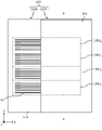
- FIG. 6A is a plan view schematically showing an example of an optical device according to the embodiment of the present disclosure.
- FIG. 6B is a plan view showing a state in which the superstructure is removed from the structure shown in FIG. 6A.
- FIG. 6C is an enlarged plan view of a part of the second optical waveguide unit shown in FIG. 6B.
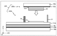
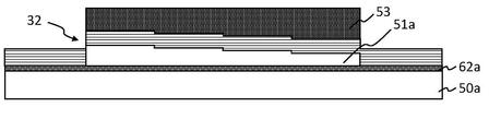
- FIG. 7A is a diagram schematically showing the structure of the cross section taken along the line AA of FIG. 6A in the state before the upper structure and the lower structure shown in FIG. 6A are bonded together.
- FIG. 6A is a plan view schematically showing an example of an optical device according to the embodiment of the present disclosure.
- FIG. 6B is a plan view showing a state in which the superstructure is removed from the structure shown in FIG. 6A.
- FIG. 6C is an enlarged plan view of
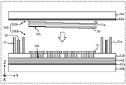
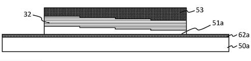
- FIG. 7B is a diagram schematically showing the structure of the cross section taken along the line BB of FIG. 6A in the state before the upper structure and the lower structure shown in FIG. 6A are bonded together.
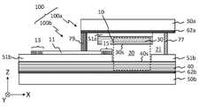
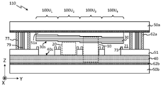
- FIG. 7C is a diagram schematically showing the structure of the cross section taken along the line CC of FIG. 6A in the state before the upper structure and the lower structure shown in FIG. 6A are bonded together.
- FIG. 8A is a diagram schematically showing the structure of the cross section taken along the line AA of FIG. 6A in a state where the upper structure and the lower structure shown in FIG. 6A are bonded to each other.
- FIG. 8B is a diagram schematically showing the structure of the cross section taken along the line BB of FIG.
- FIG. 8C is a diagram schematically showing the structure of the cross section taken along the line CC of FIG. 6A in a state where the upper structure and the lower structure shown in FIG. 6A are bonded to each other.
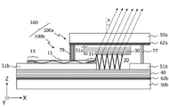
- FIG. 8D is an enlarged cross-sectional view of the second optical waveguide unit shown in FIG. 8C.
- FIG. 9 is a cross-sectional view schematically showing how light is emitted from an optical device.
- FIG. 10 is a graph showing the relationship between the emission angle of the light emitted from the optical device and the thickness of the optical waveguide region.
- FIG. 11 is a plan view schematically showing an example of an optical device according to the present embodiment.
- FIG. 12 is a perspective view schematically showing an example of a wide range of optical scans using the optical device according to the present embodiment.
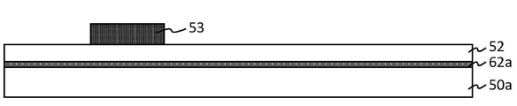
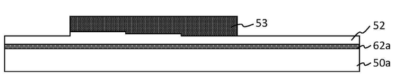
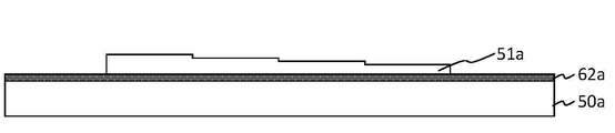
- FIG. 13A is a diagram for explaining an example of a manufacturing process of the superstructure.
- FIG. 13B is a diagram for explaining an example of a manufacturing process of the superstructure.
- FIG. 13C is a diagram for explaining an example of a manufacturing process of the superstructure.
- FIG. 13D is a diagram for explaining an example of a manufacturing process of the superstructure.
- FIG. 13E is a diagram for explaining an example of a manufacturing process of the superstructure.
- FIG. 13F is a diagram for explaining an example of a manufacturing process of the superstructure.
- FIG. 13G is a diagram for explaining an example of a manufacturing process of the superstructure.
- FIG. 13H is a diagram for explaining an example of a manufacturing process of the superstructure.
- FIG. 13I is a diagram for explaining an example of a manufacturing process of the superstructure.
- FIG. 13J is a diagram for explaining an example of a manufacturing process of the superstructure.
- FIG. 13K is a diagram for explaining an example of a manufacturing process of the superstructure.
- FIG. 13L is a diagram for explaining an example of a manufacturing process of the superstructure.
- FIG. 13M is a diagram for explaining an example of a manufacturing process of the superstructure.
- FIG. 13N is a diagram for explaining an example of a manufacturing process of the superstructure.
- FIG. 14A is a plan view schematically showing an example of an optical device according to this modification when viewed from the Z direction.
- FIG. 14A is a plan view schematically showing an example of an optical device according to this modification when viewed from the Z direction.
- FIG. 14B is a plan view showing a state in which the superstructure is removed from the structure shown in FIG. 14A.
- FIG. 14C is a diagram schematically showing the structure of the cross section taken along the line AA of FIG. 14A.
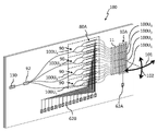
- FIG. 15 is a diagram showing a configuration example of an optical scan device in which the configurations shown in FIG. 11 are integrated on a circuit board.
- FIG. 16 is a schematic diagram showing a state in which a two-dimensional scan is performed by irradiating a light beam such as a laser at a distance from the light scanning device.
- FIG. 17 is a block diagram showing a configuration example of a LiDAR system capable of generating a ranging image.
- the present inventor has found that a conventional optical scanning device has a problem that it is difficult to scan a space with light without complicating the configuration of the device.
- the present inventor paid attention to the above-mentioned problems in the prior art, and examined the configuration for solving these problems.
- the present inventor has found that the above problem can be solved by using a waveguide element having a pair of facing mirrors and an optical waveguide layer sandwiched between the mirrors.
- One of the pair of mirrors in the waveguide element has a higher light transmittance than the other, and emits a part of the light propagating in the optical waveguide layer to the outside.
- the direction (or emission angle) of the emitted light can be changed by adjusting the refractive index or thickness of the optical waveguide layer or the wavelength of the light input to the optical waveguide layer, as described later. More specifically, by changing the refractive index, thickness, or wavelength, the component of the wave vector of the emitted light in the direction along the longitudinal direction of the optical waveguide layer can be changed. This realizes a one-dimensional scan.
- a two-dimensional scan can be realized. More specifically, by giving an appropriate phase difference to the light supplied to the plurality of waveguide elements and adjusting the phase difference, it is possible to change the direction in which the light emitted from the plurality of waveguide elements strengthens each other. can. Due to the change in the phase difference, the component of the wave vector of the emitted light in the direction intersecting the longitudinal direction of the optical waveguide layer changes. This makes it possible to realize a two-dimensional scan. 2 You can perform a two-dimensional scan. As described above, according to the embodiment of the present disclosure, it is possible to realize a two-dimensional scan by light with a relatively simple configuration.
- any one of the refractive index, thickness, and wavelength is selected from the group consisting of the refractive index of the optical waveguide layer, the thickness of the optical waveguide layer, and the wavelength input to the optical waveguide layer. Means at least one that is done. In order to change the emission direction of light, any one of the refractive index, the thickness, and the wavelength may be controlled independently. Alternatively, any two or all of these three may be controlled to change the light emission direction. In each of the following embodiments, the wavelength of the light input to the optical waveguide layer may be controlled in place of or in addition to the control of the refractive index or the thickness.
- the above basic principle can be applied not only to applications that emit light but also to applications that receive optical signals.
- the direction of the light that can be received can be changed one-dimensionally.
- the phase difference of light is changed by a plurality of phase shifters connected to a plurality of waveguide elements arranged in one direction, the direction of light that can be received can be changed two-dimensionally.
- the optical scanning device and the optical receiving device can be used as an antenna in an optical detection system such as a LiDAR (Light Detection and Ringing) system. Since the LiDAR system uses short wavelength electromagnetic waves (visible light, infrared rays, or ultraviolet rays) as compared with radar systems using radio waves such as millimeter waves, it is possible to detect the distance distribution of an object with high resolution.
- a LiDAR system can be mounted on a moving body such as an automobile, a UAV (Unmanned Aerial Vehicle, so-called drone), or an AGV (Automated Guided Vehicle), and can be used as one of collision avoidance techniques.
- an optical scanning device and an optical receiving device may be collectively referred to as an "optical device”.
- a device used for an optical scanning device or an optical receiving device may also be referred to as an "optical device”.
- light refers to electromagnetic waves including not only visible light (wavelength of about 400 nm to about 700 nm) but also ultraviolet rays (wavelength of about 10 nm to about 400 nm) and infrared rays (wavelength of about 700 nm to about 1 mm). means.
- ultraviolet light may be referred to as “ultraviolet light” and infrared light may be referred to as “infrared light”.
- scanning by light means changing the direction of light.
- One-dimensional scan means changing the direction of light linearly along a direction that intersects that direction.
- Tele-dimensional scanning means changing the direction of light two-dimensionally along a plane that intersects the direction.
- FIG. 1 is a perspective view schematically showing the configuration of the optical scan device 100.
- the optical scan device 100 includes a waveguide array including a plurality of waveguide elements 10.
- Each of the plurality of waveguide elements 10 has a shape extending in the X direction.
- the plurality of waveguide elements 10 are regularly arranged in the Y direction.
- the plurality of waveguide elements 10 propagate the light in the X direction and emit the light in the direction D3 intersecting the virtual plane parallel to the XY plane.
- the direction in which the waveguide element 10 extends and the arrangement direction of the waveguide elements 10 are orthogonal to each other, but the two may not be orthogonal to each other.
- a plurality of waveguide elements 10 are arranged at equal intervals in the Y direction, but they do not necessarily have to be arranged at equal intervals.
- Each of the plurality of waveguide elements 10 has a first mirror 30 and a second mirror 40 facing each other, and an optical waveguide layer 20 located between the mirror 30 and the mirror 40.
- Each of the mirror 30 and the mirror 40 has a reflective surface that intersects the direction D3 at the interface with the optical waveguide layer 20.
- the mirror 30, the mirror 40, and the optical waveguide layer 20 have a shape extending in the X direction.
- the plurality of first mirrors 30 of the plurality of waveguide elements 10 may be a plurality of parts of the mirror integrally configured.
- the plurality of second mirrors 40 of the plurality of waveguide elements 10 may be a plurality of parts of the mirror integrally configured.
- the plurality of optical waveguide layers 20 of the plurality of waveguide elements 10 may be a plurality of portions of the integrally configured optical waveguide layer. At least, (1) each first mirror 30 is configured separately from the other first mirror 30, and (2) each second mirror 40 is configured separately from the other second mirror 40. (3) Since each optical waveguide layer 20 is configured separately from the other optical waveguide layer 20, a plurality of waveguides can be formed.
- the term "composed of separate bodies" includes not only the fact that they are physically arranged with a space apart, but also that they are separated by a material having a different refractive index between them.
- the reflective surface of the first mirror 30 and the reflective surface of the second mirror 40 face each other almost in parallel.
- the first mirror 30 has a property of transmitting a part of the light propagating through the optical waveguide layer 20.
- the first mirror 30 has a higher light transmittance than the second mirror 40 for the light. Therefore, a part of the light propagating through the optical waveguide layer 20 is emitted to the outside from the first mirror 30.
- Such mirrors 30 and 40 can be, for example, multilayer mirrors formed of a multilayer film made of a dielectric (sometimes referred to as a "multilayer reflective film").
- the phase of the light input to each waveguide element 10 is controlled, and the refractive index or thickness of the optical waveguide layer 20 in these waveguide elements 10 or the wavelength of the light input to the optical waveguide layer 20 is synchronized. By changing the wavelengths at the same time, it is possible to realize a two-dimensional scan using light.
- the present inventor analyzed the operating principle of the waveguide element 10 in order to realize such a two-dimensional scan. Based on the result, we succeeded in realizing a two-dimensional scan by light by driving a plurality of waveguide elements 10 in synchronization.
- each waveguide element 10 when light is input to each waveguide element 10, light is emitted from the emission surface of each waveguide element 10.
- the emission surface is located on the opposite side of the reflection surface of the first mirror 30.
- the direction D3 of the emitted light depends on the refractive index, the thickness, and the wavelength of the light of the optical waveguide layer.
- at least one of the refractive index, the thickness, and the wavelength of each optical waveguide layer is synchronously controlled so that the light emitted from each waveguide element 10 is in substantially the same direction.
- the X-direction component of the wave number vector of the light emitted from the plurality of waveguide elements 10 can be changed.
- the direction D3 of the emitted light can be changed along the direction 101 shown in FIG.
- the emitted light interferes with each other.
- the direction in which the light strengthens due to interference can be changed. For example, when a plurality of waveguide elements 10 having the same size are arranged at equal intervals in the Y direction, light having a different phase is input to the plurality of waveguide elements 10 by a fixed amount. By changing the phase difference, the component in the Y direction of the wave vector of the emitted light can be changed.
- the direction D3 in which the emitted light is strengthened by interference can be changed along the direction 102 shown in FIG. .. This makes it possible to realize a two-dimensional scan using light.
- FIG. 2 is a diagram schematically showing an example of a cross-sectional structure of one waveguide element 10 and propagating light.
- the directions perpendicular to the X and Y directions shown in FIG. 1 are defined as the Z direction, and a cross section parallel to the XZ plane of the waveguide element 10 is schematically shown.
- the first mirror 30 and the second mirror 40 are arranged so as to sandwich the optical waveguide layer 20.
- the first mirror 30 has a first reflecting surface 30s.
- the second mirror 40 has a second reflecting surface 40s facing the first reflecting surface 30s.
- the light 20L introduced from one end of the optical waveguide layer 20 in the X direction is the first reflecting surface 30s of the first mirror 30 provided on the upper surface (upper surface in FIG. 2) of the optical waveguide layer 20 and the lower surface (FIG. 2). It propagates in the optical waveguide layer 20 while repeating reflection by the second reflecting surface 40s of the second mirror 40 provided on the lower surface of No. 2.
- the light transmittance of the first mirror 30 is higher than the light transmittance of the second mirror 40. Therefore, a part of the light can be mainly output from the first mirror 30.
- the light propagation angle means the angle of incidence on the interface between the mirror 30 or the mirror 40 and the optical waveguide layer 20.
- Light that is incident at an angle closer to perpendicular to the mirror 30 or the mirror 40 can also propagate. That is, light incident on the interface can also propagate at an angle smaller than the critical angle of total reflection. Therefore, the group velocity of light in the propagation direction of light is significantly lower than the speed of light in free space.
- the waveguide element 10 has the property that the light propagation conditions change significantly with respect to changes in the wavelength of light, the thickness of the optical waveguide layer 20, and the refractive index of the optical waveguide layer 20.
- a waveguide is referred to as a "reflecting waveguide” or a “slow light waveguide”.
- the emission angle ⁇ of the light emitted from the waveguide element 10 into the air is expressed by the following equation (1).
- the emission direction of the light is changed by changing any one of the wavelength ⁇ of the light in the air, the refractive index n w of the optical waveguide layer 20, and the thickness d of the optical waveguide layer 20. Can be done.
- the emission angle is 0 °.
- the emission angle changes to about 66 °.
- the emission angle changes to about 51 °.
- the emission angle changes to about 30 °. In this way, by changing any one of the wavelength ⁇ of the light, the refractive index n w of the optical waveguide layer 20, and the thickness d of the optical waveguide layer 20, the emission direction of the light can be significantly changed.
- the optical scan device 100 controls at least one of the wavelength ⁇ of the light input to the optical waveguide layer 20, the refractive index n w of the optical waveguide layer 20, and the thickness d of the optical waveguide layer 20. Controls the emission direction of light.
- the wavelength ⁇ of light may remain constant during operation without change. In that case, light scanning can be realized with a simpler configuration.
- the wavelength ⁇ is not particularly limited.
- the wavelength ⁇ is a wavelength of 400 nm to 1100 nm (that is, visible light to near-infrared light), which provides high detection sensitivity with a photodetector or image sensor that detects light by absorbing light with general silicon (Si). Can be included in the region.
- the wavelength ⁇ may be included in the wavelength range of near-infrared light from 1260 nm to 1625 nm, which has a relatively low transmission loss in an optical fiber or Si waveguide. Note that these wavelength ranges are examples.
- the wavelength range of the light used is not limited to the wavelength range of visible light or infrared light, and may be, for example, the wavelength range of ultraviolet light.
- the optical scan device 100 may include a first adjusting element that changes at least one of the refractive index, thickness, and wavelength of the optical waveguide layer 20 in each waveguide element 10.
- the light emission direction can be significantly changed by changing at least one of the refractive index n w , the thickness d, and the wavelength ⁇ of the optical waveguide layer 20. ..
- the emission angle of the light emitted from the mirror 30 can be changed in the direction along the waveguide element 10.
- the optical waveguide layer 20 may include a liquid crystal material or an electro-optical material.
- the optical waveguide layer 20 may be sandwiched by a pair of electrodes. By applying a voltage to the pair of electrodes, the refractive index of the optical waveguide layer 20 can be changed.
- At least one actuator may be connected to at least one of the mirror 30 and the mirror 40 in order to adjust the thickness of the optical waveguide layer 20.
- the thickness of the optical waveguide layer 20 can be changed by changing the distance between the mirror 30 and the mirror 40 by at least one actuator. If the optical waveguide layer 20 is formed of a liquid, the thickness of the optical waveguide layer 20 can be easily changed.
- FIG. 3A is a diagram showing a cross section of a waveguide array that emits light in a direction perpendicular to the emission surface of the waveguide array.
- FIG. 3A also shows the phase shift amount of the light propagating through each waveguide element 10.
- the phase shift amount is a value based on the phase of the light propagating through the waveguide element 10 at the left end.
- the waveguide array in this embodiment includes a plurality of waveguide elements 10 arranged at equal intervals.
- the dashed arc indicates the wavefront of light emitted from each waveguide element 10.
- the straight line shows the wavefront formed by the interference of light.
- the arrows indicate the direction of the light emitted from the waveguide array (ie, the direction of the wave vector).
- the phases of the light propagating in the optical waveguide layer 20 in each waveguide element 10 are the same.
- the light is emitted in a direction (Z direction) perpendicular to both the arrangement direction (Y direction) of the waveguide element 10 and the direction (X direction) in which the optical waveguide layer 20 extends.
- FIG. 3B is a diagram showing a cross section of a waveguide array that emits light in a direction different from the direction perpendicular to the emission plane of the waveguide array.
- the phases of the light propagating in the optical waveguide layer 20 in the plurality of waveguide elements 10 are different by a fixed amount ( ⁇ ) in the arrangement direction.
- the light is emitted in a direction different from the Z direction.
- ⁇ the component in the Y direction of the wave vector of light can be changed.
- the light emission angle ⁇ 0 is expressed by the following equation (2).
- the direction of the light emitted from the optical scan device 100 is not parallel to the XZ plane or the YZ plane. That is, ⁇ ⁇ 0 ° and ⁇ 0 ⁇ 0 °.
- FIG. 4 is a perspective view schematically showing a waveguide array in a three-dimensional space.
- the thick arrow shown in FIG. 4 indicates the direction of the light emitted from the optical scanning device 100.
- ⁇ is the angle formed by the light emission direction and the YZ plane.
- ⁇ satisfies equation (1).
- ⁇ 0 is the angle formed by the light emission direction and the XZ plane.
- ⁇ 0 satisfies the equation (2).
- phase shifter that changes the phase of the light may be provided before introducing the light into the waveguide element 10.
- the optical scan device 100 includes a plurality of phase shifters connected to each of the plurality of waveguide elements 10, and a second adjusting element for adjusting the phase of light propagating through each phase shifter.
- Each phase shifter includes a waveguide connected directly to or via another waveguide to the optical waveguide layer 20 in the corresponding one of the plurality of waveguide elements 10.
- the second adjusting element changes the direction D3 of the light emitted from the plurality of waveguide elements 10 by changing the phase difference of the light propagating from the plurality of phase shifters to the plurality of waveguide elements 10, respectively.
- a plurality of arranged phase shifters are also referred to as "phase shifter arrays”.
- FIG. 5 is a schematic view of the waveguide array 10A and the phase shifter array 80A as viewed from the normal direction (Z direction) of the light emitting surface.
- all phase shifters 80 have the same propagation characteristics and all waveguide elements 10 have the same propagation characteristics.
- Each phase shifter 80 and each waveguide element 10 may have the same length or may have different lengths.
- the respective phase shift amounts can be adjusted by the drive voltage. Further, by adopting a structure in which the length of each phase shifter 80 is changed in equal steps, it is possible to give a phase shift in equal steps with the same drive voltage.
- the optical scan device 100 drives an optical turnout 90 that branches and supplies light to a plurality of phase shifters 80, a first drive circuit 70a that drives each waveguide element 10, and each phase shifter 80.
- a second drive circuit 70b is further provided.
- the straight arrow in FIG. 5 indicates the input of light.
- Two-dimensional scanning can be realized by independently controlling the first drive circuit 70a and the second drive circuit 70b provided separately.
- the first drive circuit 70a functions as one element of the first adjustment element
- the second drive circuit 70b functions as one element of the second adjustment element.
- the first drive circuit 70a changes the angle of light emitted from the optical waveguide layer 20 by changing at least one of the refractive index and the thickness of the optical waveguide layer 20 in each waveguide element 10.
- the second drive circuit 70b changes the phase of the light propagating inside the optical waveguide layer 20 by changing the refractive index of the optical waveguide layer 20 in each phase shifter 80.
- the optical turnout 90 may be configured by a waveguide in which light is propagated by total internal reflection, or may be configured by a reflection type waveguide similar to the waveguide element 10.
- each light may be introduced into the phase shifter 80.
- a passive phase control structure by adjusting the length of the waveguide leading up to the phase shifter 80 can be used.
- a phase shifter that has the same function as the phase shifter 80 and can be controlled by an electric signal may be used.
- the phase may be adjusted before being introduced into the phase shifter 80 so that the light having the same phase is supplied to all the phase shifters 80.
- the control of each phase shifter 80 by the second drive circuit 70b can be simplified.
- An optical device having the same configuration as the above-mentioned optical scan device 100 can also be used as an optical receiving device. Details such as the operating principle and operating method of the optical device are disclosed in US Patent Application Publication No. 2018/0224709. The entire disclosure of this document is incorporated herein by reference.
- the optical device 100 can be manufactured, for example, by laminating an upper structure including a first mirror 30 and a lower structure including a second mirror 40.
- a sealing member such as an ultraviolet curable resin or a thermosetting resin can be used.
- a region corresponding to the above-mentioned optical waveguide layer is formed between the upper structure and the lower structure.
- the region is referred to as an "optical waveguide region".
- the optical waveguide region may include, for example, a liquid crystal material.
- vacuum encapsulation can be utilized to inject the liquid crystal material into the optical device 100.
- the liquid crystal material can be injected into the space surrounded by the sealing member. According to such a method, vacuum leakage can be prevented when the liquid crystal material is injected.
- the distance between the upper structure and the lower structure does not match the design value, and an error may occur, depending on the accuracy of the bonding. Due to this error, the manufactured optical device may not achieve the performance as designed, for example with respect to the emission angle and / or the intensity of the emitted light.
- the optical device has the following configurations in order to solve this problem.
- the optical device includes a plurality of optical waveguide units.
- Each of the plurality of optical waveguide units includes a first mirror 30, a second mirror 40, and at least one optical waveguide region located between them.
- the distance between the reflecting surface 30s of the first mirror 30 and the reflecting surface 40s of the second mirror 40 is different for each optical waveguide unit.
- the distance between the reflecting surface 30s of the first mirror 30 and the reflecting surface 40s of the second mirror 40 (hereinafter, also referred to as “mirror spacing”) in each optical waveguide unit is designed to be slightly different for each optical waveguide unit. obtain.
- each optical waveguide unit may be designed so that the design value of the mirror spacing differs by a fixed amount ⁇ d for each optical waveguide unit.
- ⁇ d is set to an appropriate value according to the number of optical waveguide units and the maximum value of the allowable error, as will be described in detail later.
- the mirror spacing may be within the allowable range in at least one other optical waveguide unit. Can be high.
- the optical device includes a plurality of optical waveguide units arranged along the first direction.
- Each of the plurality of optical waveguide units includes a first mirror having a first reflecting surface, a second mirror having a second reflecting surface facing the first reflecting surface, the first mirror, and the second mirror. It comprises at least one optical waveguide region located between. The distance between the first reflecting surface and the second reflecting surface is different for each optical waveguide unit.
- At least one of the plurality of optical waveguide units is optically coupled to the optical waveguide region, and light is input to the optical waveguide region. At least one optical input waveguide is provided.
- light can be input to the optical waveguide region in each of the plurality of optical waveguide units.
- the optical input waveguide is connected to the optical waveguide region via a mode converter in the optical device according to the second item.
- the mode converter can improve the efficiency of optical coupling from the optical input waveguide to the optical waveguide region.
- the optical device according to the fourth item is the optical device according to the third item, and the mode converter includes a grating.
- the grating comprises a structure in which the refractive index changes periodically along a second direction intersecting the first direction.
- the efficiency of optical coupling from the optical input waveguide to the optical waveguide region can be improved by appropriately designing the grating configuration.
- the optical device according to the fifth item is the optical device according to the third or fourth item, via the mode converter from the optical input waveguide to the optical waveguide region in at least one of the plurality of optical waveguide units.
- the efficiency of the optical coupling is 80% or more.
- light can be coupled to the optical waveguide region in at least one of a plurality of optical waveguide units with high efficiency.
- the efficiency of the optical coupling in the optical waveguide unit adjacent to at least one of the plurality of optical waveguide units is less than 80%.
- light can be coupled to the optical waveguide region with high efficiency only in a part of the optical waveguide units among the plurality of optical waveguide units.
- the optical device according to the seventh item is the optical device according to any one of the first to sixth items, in which the distance between the first reflecting surface and the second reflecting surface is along the first direction. It changes monotonously.
- the distance between the first mirror and the second mirror can be made different for each optical waveguide unit by the mirror having a multi-stage structure.
- the distance between the first reflecting surface and the second reflecting surface changes by a constant amount along the first direction. ..
- the optical device according to the ninth item has a higher transmittance than the second mirror in the optical device according to any one of the first to eighth items.
- a part of the light propagating in the optical waveguide region can be emitted to the outside through the first mirror.
- the optical device is the optical device according to the ninth item, wherein each of the plurality of optical waveguide units includes a first electrode and a second electrode, and the first mirror and the second mirror. Contains liquid crystal material between.
- the optical waveguide region is filled with the liquid crystal material.
- the direction of the light emitted through the first mirror or the light captured in the optical waveguide region via the first mirror can be changed.
- the optical device according to the eleventh item is the optical device according to any one of the first to tenth items, the first structure including the first mirror included in each of the plurality of optical waveguide units, and the said.
- the first reflecting surface and the second reflecting surface can be made substantially parallel by bonding the first structure and the second structure via the support member.
- the optical device according to the twelfth item is the optical device according to the eleventh item, in which the support member is formed of an elastic material.
- the first reflective surface and the second reflective surface can be made almost parallel by the support member formed of the elastic material.
- the optical device according to the thirteenth item selectively directs light to the optical waveguide region included in at least one of the plurality of optical waveguide units in the optical device according to any one of the first to twelfth items. Equipped with an optical switch that can be supplied to.
- At least one of a plurality of optical waveguide units can be selectively used.
- the optical device according to the fourteenth item is the optical device according to any one of the first to thirteenth items, in which light is supplied only to a part of the optical waveguide units among the plurality of optical waveguide units, and other optical waveguide units are supplied. No light is supplied to the optical waveguide unit.
- the efficiency of optical coupling to the optical waveguide region in some of the optical waveguide units is 80% or more in the optical device according to the fourteenth item.
- the optical device includes an optical device according to any one of the first to fifteenth items, a photodetector that detects light emitted from the optical device and reflected from an object, and the light. It includes a signal processing circuit that generates distance distribution data based on the output of the detector.
- This light detection system can generate a distance image.
- all or part of a circuit, unit, device, member or part, or all or part of a functional block in a block diagram is, for example, a semiconductor device, a semiconductor integrated circuit (IC), or an LSI (lage scale integration). ) Can be performed by one or more electronic circuits.
- the LSI or IC may be integrated on one chip, or may be configured by combining a plurality of chips.
- functional blocks other than the storage element may be integrated on one chip.
- it is called LSI or IC, but the name changes depending on the degree of integration, and it may be called system LSI, VLSI (very large scale integration), or ULSI (ultra large scale integration).
- a Field Programmable Gate Array (FPGA) programmed after the LSI is manufactured, or a reconfigurable logic device that can reconfigure the connection relationship inside the LSI or set up the circuit partition inside the LSI can also be used for the same purpose.
- FPGA Field Programmable Gate Array
- all or part of the function or operation of a circuit, unit, device, member or part can be executed by software processing.
- the software is recorded on a non-temporary recording medium such as one or more ROMs, optical disks, hard disk drives, etc., and when the software is run by a processor, the functions identified by the software It is performed by a processor and peripherals.
- the system or device may include one or more non-temporary recording media on which the software is recorded, a processor, and the required hardware device, such as an interface.
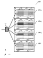
- FIG. 6A is a plan view schematically showing an example of the optical device 100 according to the embodiment of the present disclosure.
- the optical device 100 includes an upper structure 100a and a lower structure 100b.
- FIG. 6B is a plan view showing a state in which the superstructure 100a is removed from the structure shown in FIG. 6A.
- the side where the upper structure 100a is located is referred to as "upper part”, and the side where the lower structure 100b is located is referred to as “lower part”.
- the terms “upper” and “lower” are used for convenience of explanation and do not limit the posture of the optical device 100 when in use. Regardless of these terms, the posture of the optical device 100 can be arbitrarily determined according to the application.
- the upper structure 100a is also referred to as a “first structure”
- the lower structure 100b is also referred to as a “second structure”.
- the optical device 100 of the present embodiment includes a first optical waveguide unit 100U 1 , a second optical waveguide unit 100U 2 , a third optical waveguide unit 100U 3 , and a fourth optical waveguide unit 100U. 4 is provided.
- these optical waveguide units are also collectively referred to as "optical waveguide unit 100U" without distinction.
- the first optical waveguide unit 100U 1 to the fourth optical waveguide unit 100U 4 are arranged in the area surrounded by the broken line shown in FIGS. 6A and 6B.
- the number of the optical waveguide units 100U is not limited to four, and may be any number of two or more.
- FIG. 6C is an enlarged plan view of a part of the second optical waveguide unit 100U 2 shown in FIG. 6B.
- FIGS. 7A, 7B, and 7C are diagrams schematically showing the cross-sectional structure of the optical device 100 in the state before the upper structure 100a and the lower structure 100b shown in FIG. 6A are bonded together.
- the cross sections shown in FIGS. 7A to 7C correspond to the AA line cross section, the B-line cross section, and the CC line cross section of FIG. 6A, respectively.
- the downward arrows shown in FIGS. 7A to 7C indicate that the upper structure 100a is attached to the lower structure 100b.
- FIGS. 8A to 8C are diagrams schematically showing a cross-sectional structure of the optical device 100 in a state where the upper structure 100a and the lower structure 100b are bonded together.
- 8A to 8C show the structures of the AA line cross section, the BB line cross section, and the CC line cross section in FIG. 6A, respectively.
- FIG. 8D is an enlarged cross-sectional view of the second optical waveguide unit 100U 2 shown in FIG. 8C.
- the superstructure 100a includes a first substrate 50a, a first electrode 62a, a dielectric layer 51a, and a first mirror 30.
- the first electrode 62a, the first dielectric layer 51a, and the first mirror 30 are provided on the first substrate 50a in this order.
- the dielectric layer 51a and the first mirror 30 have a multi-stage structure having a step at the boundary portion of the optical waveguide unit 100U.
- the lower structure 100b includes a second substrate 50b, a second electrode 62b, a second mirror 40, a second dielectric layer 51b, a plurality of partition walls 73, a plurality of elastic spacers 77, a sealing member 79, and a plurality of optical waveguides 11.
- a second electrode 62b is provided on the second substrate 50b.
- a second mirror 40 is provided on the second electrode 62b.
- the reflective surface 40s of the second mirror 40 faces the reflective surface 30s of the first mirror 30.
- a second dielectric layer 51b is provided on the second mirror 40. A part of the second dielectric layer 51b is removed to expose a part of the reflecting surface 40s of the mirror 40.
- a plurality of partition walls 73, a plurality of elastic spacers 77, a sealing member 79, and a plurality of optical waveguides 11 are provided on the second dielectric layer 51b.
- the upper structure 100a and the lower structure 100b can be manufactured by, for example, a semiconductor process.
- the semiconductor process may include steps such as film formation by sputtering and vapor deposition, photolithography, and etching.
- the upper structure 100a and the lower structure 100b are bonded together in the manufacturing process of the optical device 100. Further, as shown in FIGS. 8A to 8C, the space sandwiched between the upper structure 100a and the lower structure 100b is filled with the liquid crystal material 21. In this way, the optical device 100 is manufactured. A part of the space filled with the liquid crystal material 21 is the optical waveguide region 20.
- the plurality of elastic spacers 77 are useful for arranging the first substrate 50a and the second substrate 50b in parallel at predetermined intervals in the bonding step. However, an error may occur in the distance between the substrate 50a and the substrate 50b.
- the distance between the first mirror 30 and the second mirror 40 in each optical waveguide unit 100U may be out of the allowable range. In that case, the direction or intensity of the light emitted from the optical waveguide unit 100U deviates from the design value, and the desired performance cannot be realized.
- a plurality of optical waveguide regions 20 are formed between the reflection surface 30s of the first mirror 30 and the reflection surface 40s of the second mirror 40. These optical waveguide regions 20 are partitioned by a partition wall 73.
- the dimension, that is, the thickness of each optical waveguide region 20 in the Z direction is equal to the distance between the reflecting surface 30s of the first mirror 30 and the reflecting surface 40s of the second mirror 40.
- the dimension, or width, of each optical waveguide region 20 in the Y direction is equal to the distance between the sides of the two partition walls 73 located on either side of the optical waveguide region 20.
- the portion of the first mirror 30 that overlaps the optical waveguide region 20 when viewed from the Z direction, the portion of the second mirror 40 that overlaps the optical waveguide region 20 when viewed from the Z direction, and the optical waveguide region 20 are optical waveguides.
- the optical waveguide functions as the above-mentioned waveguide element 10, that is, a slow light waveguide. In the following description, this optical waveguide will be referred to as "optical waveguide 10".
- each optical waveguide unit 100U has a first substrate 50a, a first electrode 62a, a first dielectric layer 51a, a first mirror 30, a second substrate 50b, a second electrode 62b, and a second mirror 40. , A second dielectric layer 51b, a plurality of optical waveguide regions 20, and a plurality of partition walls 73.
- Each optical waveguide unit 100U further includes a plurality of optical waveguides 11 connected to the plurality of optical waveguide regions 20, as shown in FIG. 6C.
- the first mirror 30 included in each optical waveguide unit 100U is a part of the first mirror 30 included in the optical device 100.
- the plurality of optical waveguide regions 20 included in each optical waveguide unit 100U are a part of the plurality of optical waveguide regions 20 included in the optical device 100.
- the distance between the reflecting surface 30s of the mirror 30 and the reflecting surface 40s of the mirror 40, that is, the mirror spacing is different for each optical waveguide unit 100U.
- the mirror spacing of the first optical waveguide unit 100U 1 is the widest, and the mirror spacing is gradually increased in the order of the second optical waveguide unit 100U 2 , the third optical waveguide unit 100U 3 , and the fourth optical waveguide unit 100U 4 .
- a plurality of steps are formed in the first dielectric layer 51a so that such a structure is realized.
- a similar step is generated on the surface of the first mirror 30, and a structure in which the mirror spacing differs for each optical waveguide unit 100U is realized.
- the design value of the mirror spacing of each optical waveguide unit 100U can be set to a different value by, for example, a constant value ⁇ d. ⁇ d is set to an appropriate value according to the number of optical waveguide units and the maximum value of the allowable error, as will be described in detail later. Even if there is an error in the distance between the first substrate 50a and the second substrate 50b due to such a design, the reflection surface 30s of the first mirror 30 and the reflection of the second mirror 40 in at least one optical waveguide unit 100U.
- the distance from the surface 40s can be kept within an allowable range.
- the light is emitted as designed, for example, with respect to the emission angle and / or the intensity of the emitted light. It can be emitted from 100.
- light may be supplied only to a selected optical waveguide unit among the plurality of optical waveguide units 100U, and light may not be supplied to the other optical waveguide units.
- the part of the optical waveguide unit is, for example, an optical waveguide unit having an optical coupling efficiency of 80% or more to the optical waveguide region 20.
- some of the optical waveguide units are optical waveguide units having a scannable angle width of 30 ° or more.
- the optical waveguide unit 100U to which light is not supplied is a dummy and is not used.
- the optical waveguide unit 100U to which light is not supplied is separated from the light source that inputs the light.
- the plurality of optical waveguide units 100U in the present embodiment are connected to each other to form a single structure. Not limited to such a structure, the plurality of optical waveguide units 100U may be physically separated. As shown in FIG. 8C, the plurality of optical waveguide units 100U in the present embodiment are lined up without a gap along the Y direction, but may be lined up with a gap. The dimensions of each optical waveguide unit 100U in the Y direction may be uniform or non-uniform.
- the number of the optical waveguide units 100U is not limited to four, and may be any number of two or more. The number of optical waveguide units 100U may be, for example, 2 or more and 10 or less.
- the substrate on which light is emitted has translucency. Both the substrates 50a and 50b may have translucency.
- the electrode on which light is emitted has translucency. Both the electrodes 62a and 62b may have translucency. At least one of the electrodes 62a and 62b can be formed, for example, from a transparent electrode.
- the dielectric layers 51a and 51b the dielectric layer on the side from which light is emitted has translucency. Both the dielectric layers 51a and 51b may have translucency.
- light is emitted from the plurality of optical waveguides 10 via the dielectric layer 51a, the electrodes 62a, and the substrate 50a in the superstructure 100a.
- the plurality of partition walls 73 are provided on the dielectric layer 51b.
- the plurality of partition walls 73 are arranged in the Y direction.
- Each of the plurality of partition walls 73 has a structure extending along the X direction.
- a part of the dielectric layer 51b located between the plurality of partition walls 73 when viewed from the Z direction is removed.
- a plurality of portions of the reflective surface 40s of the mirror 40 are exposed. Multiple exposed parts are lined up in the Y direction.
- Each of the plurality of exposed portions has a shape extending along the X direction. As shown in FIG.
- the portion of the dielectric layer 51b that has not been removed and the partition wall 73 immediately above the dielectric layer 51b form a convex portion extending in the X direction. Therefore, a plurality of convex portions arranged in the Y direction are formed on the mirror 40.
- the upper surface of the convex portion is not in contact with the reflective surface of the mirror 30, but may be in contact with the reflective surface.
- a plurality of concave portions are formed between the plurality of convex portions.
- the recess also has a structure extending along the X direction.
- each recess that is, the height of the protrusions on both sides of each recess, can be, for example, 1 ⁇ m or more and 10 ⁇ m or less.
- the depth of the concave portion and the height of the convex portion mean the respective dimensions measured along the Z direction in the drawing.
- the plurality of optical waveguide regions 20 are defined as regions in which a plurality of recesses are located when viewed from the Z direction.
- the optical waveguide region 20 is a region surrounded by a reflecting surface 30s of the mirror 30, a reflecting surface 40s of the mirror 40, two adjacent convex portions, and a space between the two adjacent convex portions and the mirror 30.
- the optical waveguide region 20 includes a liquid crystal material 21.
- the liquid crystal material 21 is used, but other types of dielectric materials capable of changing the refractive index by applying a voltage, for example, an electro-optical material may be used.
- An alignment film that defines the orientation direction of the liquid crystal material may be formed on the reflection surface 30s and / or the reflection surface 40s.
- six optical waveguide regions 20 are arranged along the Y direction.
- the number of the optical waveguide regions 20 in each optical waveguide unit 100U is not limited to 6, and may be any number of 1 or more.
- the number of optical waveguide regions 20 in each optical waveguide unit 100U may be, for example, 1 or more and 128 or less.
- the refractive index of the optical waveguide region 20 is higher than that of the partition wall 73 and the dielectric layer 51b.
- the light propagating in the optical waveguide region 20 does not leak to the convex portions located on both sides of the optical waveguide region 20. This is because the light propagating in the optical waveguide region 20 is totally reflected at the interface between the optical waveguide region 20 and the convex portion.
- the region where the convex portion exists and the region between the convex portion and the mirror 30 can be referred to as a “non-guided region”.
- a plurality of optical waveguide regions 20 and a plurality of non-waveguide regions are alternately arranged in the Y direction between the mirror 30 and the mirror 40. With this configuration, a plurality of optical waveguides 10 arranged in the Y direction are formed.
- the electrodes 62a and 62b face each other and indirectly sandwich the optical waveguide region 20. "Indirectly sandwiching" means sandwiching through another member.
- the mirror 30 and the mirror 40 are arranged between the electrodes 62a and 62b.
- the positional relationship between the electrode 62a and the mirror 30 may be reversed. In that case, an alignment film may be formed on the surface of the electrode 62a.
- the positional relationship between the electrode 62b and the mirror 40 may be reversed.
- the refractive index of the liquid crystal material 21 can be adjusted by adjusting the voltage applied to the electrodes 62a and 62b. By changing the voltage, the emission angle of the light emitted to the outside from the optical waveguide 10 changes.
- the plurality of elastic spacers 77 are formed of an elastic material and are located around the plurality of optical waveguides 10.
- a plurality of columnar elastic spacers 77 are two-dimensionally arranged. This arrangement may be regular, periodic, or irregular.
- the elastic spacer 77 is located both inside and outside the area enclosed by the sealing member 79.
- the elastic spacer 77 may be provided only on one of the inner side and the outer side of the region. As described above, the elastic spacer 77 is located on at least one of the inside and the outside of the region. A part of the elastic spacer 77 may be provided in the optical waveguide layer 20.
- the number of elastic spacers 77 may be any number of 1 or more.
- the elastic spacer 77 may have one connected shape inside and / or outside the area enclosed by the sealing member 79. The shape can be, for example, a linear, curved, wavy, or zigzag linear shape when viewed from the Z direction.
- the dimension of the elastic spacer 77 in the Z direction is larger than the dimension of the seal member 79 in the Z direction in the state before the upper structure 100a and the lower structure 100b are bonded together. Therefore, when the upper structure 100a and the lower structure 100b are attached, the electrodes 62a of the upper structure 100a first come into contact with the elastic spacer 77 of the lower structure 100b.
- Elastic deformation occurs in the elastic spacer 77.
- the elastic modulus is defined by dividing the applied force by the generated strain.
- the elastic modulus of the elastic spacer 77 is smaller than, for example, the elastic modulus of the mirror 30 and the partition wall 73. That is, the elastic spacer 77 is more easily deformed than the mirror 30 and the partition wall 73.
- the elastic spacer 77 acts like a spring and compresses. As a result, the substrate 50a and the substrate 50b are substantially parallel to each other.
- the plurality of elastic spacers 77 are sandwiched by the upper structure 100a and the lower structure 100b, and define the distance between the reflecting surface 30s and the reflecting surface 40s.
- the elastic spacer 77 is sandwiched between the electrode 62a included in the upper structure 100a and the dielectric layer 51b included in the lower structure 100b.
- the elastic spacer 77 is also referred to as a “support member”.
- the electrode 62b and the seal member 79 first come into contact with each other, the contact point becomes a fulcrum, and the upper structure 100a can tilt with respect to the lower structure 100b.
- the substrate 50a and the substrate 50b may not be parallel to each other.
- the elastic spacer 77 makes the substrate 50a and the substrate 50b substantially parallel, an error may occur in the distance between the substrate 50a and the substrate 50b for the following reasons.
- One possible reason is that there may be variations in the dimensions of the elastic spacer 77 in the Z direction before bonding.
- Another possible reason is that the amount of deformation of the elastic spacer 77 may vary due to fluctuations in the pressure when the upper structure 100a and the lower structure 100b are bonded together.
- the seal member 79 fixes the distance between the upper structure 100a and the lower structure 100b. As shown in FIG. 6B, the seal member 79 surrounds the plurality of optical waveguide regions 20 and the plurality of partition walls 73 when viewed from the Z direction.
- the seal member 79 includes a portion extending along the Y direction and a portion extending along the X direction from both sides of the portion.
- the seal member 79 is arranged on the dielectric layer 51b, and a portion extending along the Y direction is provided so as to straddle the plurality of optical waveguides 11.
- the upper surface of the seal member 79 is parallel to the XY plane.
- the dimensions of the portion of the sealing member 79 located directly above the dielectric layer 51b in the Z direction are the thicknesses of the partition wall 73, the mirror 30, and the dielectric layer 51a (that is, the dimensions in the Z direction) as shown in FIG. 8B. ) Is greater than the sum.
- the seal member 79 can be formed of, for example, a photocurable resin such as an ultraviolet curable resin or a thermosetting resin.
- the stretchable seal member 79 before curing allows the upper structure 100a and the lower structure 100b to be bonded together without a gap. After the upper structure 100a and the lower structure 100b are bonded together, the sealing member 79 is cured by light irradiation or heating.
- the material of the sealing member 79 does not need to be a photocurable resin or a thermosetting resin as long as the distance between the substrate 50a and the substrate 50b can be maintained for a long period of time.
- the liquid crystal material 21 can be injected into the space surrounded by the sealing member 79, for example by vacuum injection. By injecting the liquid crystal material 21 into the space, it is possible to prevent vacuum leakage when the liquid crystal material 21 is injected.
- the plurality of optical waveguides 11 are each connected to the plurality of optical waveguide regions 20. Light is supplied from the optical waveguide 11 to the optical waveguide region 20.
- the optical waveguide 11 is located on the dielectric layer 51b.
- the size of the dielectric layer 51b in the Z direction can be adjusted, for example, so that the optical waveguide 11 is located near the center of the optical waveguide region 20 in the Z direction.
- the optical waveguide 11 is a waveguide that propagates light by total internal reflection. Therefore, the refractive index of the optical waveguide 11 is higher than that of the dielectric layer 51b.
- each optical waveguide unit 100U in each optical waveguide unit 100U, six optical waveguides 11 are arranged in the Y direction.
- the number of the optical waveguides 11 in the optical waveguide unit 100U is not limited to 6, and may be any number of 1 or more.
- the number of optical waveguides 11 in each optical waveguide unit 100U may be, for example, 1 or more and 128 or less.
- the optical wave guide 11 is not limited to the total reflection waveguide, and may be a slow light waveguide.
- each optical waveguide 11 in each optical waveguide unit 100U includes a tip portion located between two adjacent partition walls among a plurality of partition walls 73.
- Each optical waveguide 11 includes a grating 15 at its tip.
- the grating 15 has a periodic structure in which the refractive index of the surface changes periodically along the X direction.
- the grating 15 may include, for example, grooves that are periodically aligned in the X direction.
- the propagation constant of the light propagating in the optical waveguide 11 is different from the propagation constant of the light propagating in the optical waveguide 10.
- the grating 15 converts a part of the light propagating through the optical waveguide 11 into diffracted light.
- the propagation constant of the diffracted light is equal to the value obtained by shifting the propagation constant of the light propagating through the optical waveguide 11 by the reciprocal lattice of the periodic structure, that is, by multiplying the reciprocal of the period by 2 ⁇ . If the propagation constant of the diffracted light matches the propagation constant of the light propagating in the optical waveguide region 20, the light propagating in the optical waveguide 11 is efficiently coupled to the optical waveguide region 20. Even when these two propagation constants do not completely match, if the difference between these two propagation constants can be reduced, the optical coupling efficiency from the optical waveguide 11 to the optical waveguide region 20 via the grating 15 is improved. The optical coupling efficiency depends on the period, duty ratio, and depth of the grooves contained in the grating 15.
- the tip portion including the grating 15 may be considered as another component.
- a mode converter any configuration that improves the optical coupling efficiency.
- Such a configuration may be, for example, a tapered structure in which the tip portion narrows toward the optical waveguide region 20.
- the optical waveguide 11 is connected to the optical waveguide region 20 via a mode converter.
- Each optical waveguide 11 includes a portion that overlaps with the substrate 50b but does not overlap with the substrate 50a when viewed from the Z direction. As shown in FIG. 6C, each optical waveguide 11 may include a grating 13 at the non-overlapping portion. In the example shown in FIG. 6C, each optical waveguide 11 includes a grating 13 at the tip opposite to the tip provided with the grating 15. The portion of the optical waveguide 11 including the grating 13 may be considered as another component. The light input via the grating 13 can be coupled to the optical waveguide 11 with higher efficiency.
- the optical waveguide 11 may include a portion that overlaps with the substrate 50b but does not overlap with the substrate 50a as in the present embodiment, or may include a portion that does not overlap with both the substrate 50a and the substrate 50b. As described above, the optical waveguide 11 may include a portion that does not overlap with at least one of the substrate 50a and the substrate 50b when viewed from a direction perpendicular to the surface of each substrate. Note that light may be directly input from the light source to the end of the optical waveguide region 20 without using the optical waveguide 11.
- FIG. 9 is a cross-sectional view schematically showing how the light emitted from the optical device 100 is emitted.
- the light input via the grating 13 propagates through the optical waveguide 11 and is input to the optical waveguide region 20 via the grating 15.
- the input light is emitted to the outside through the superstructure 100a.
- the emission direction of light is parallel to the XZ plane, and the emission angle thereof is ⁇ .
- FIG. 10 is a graph showing the relationship between the emission angle of the light emitted from the optical device 100 and the thickness of the optical waveguide region 20.
- the thickness of the optical waveguide region 20 is the distance between the first mirror 30 and the second mirror 40.
- FIG. 10 shows an example of the relationship between the emission angle and the thickness calculated for the 7th waveguide mode.
- the normal light refractive index of the liquid crystal material constituting the optical waveguide region 20 is 1.512
- the abnormal light refractive index is 1.665.
- the refractive index of the optical waveguide region 20 changes in the range of 1.512 to 1.665 depending on the application of a voltage to the liquid crystal material.
- the wavelength of the light propagating in the optical waveguide region 20 is 940 nm.
- the solid line shown in FIG. 10 represents the case where the refractive index of the optical waveguide region 20 is the upper limit value 1.665, and the broken line shown in FIG. 10 indicates the case where the refractive index of the optical waveguide region 20 is the lower limit value 1.512. show.
- the angle range between the solid line and the broken line shown in FIG. 10 is the range of the scannable emission angle.
- the range of emission angles that can be scanned depends on the thickness of the optical waveguide region 20. For example, when the thickness of the optical waveguide region 20 is 2.10 ⁇ m, the scannable emission angle range is 17 ° or more and 44 ° or less.
- the scannable angle width in this case is 27 °.
- the wider the scannable angle width the more applications the optical device 100 can be used for.
- it is desirable that the scannable angle width is 30 ° or more.
- the refractive index of the optical waveguide region 20 is the lower limit value of 1.512, no light is emitted if the thickness of the optical waveguide region 20 is 2.05 ⁇ m or less. If the refractive index of the optical waveguide region 20 is made higher than 1.512, light can be emitted even when the thickness is 2.05 ⁇ m or less.
- the refractive index of the optical waveguide region 20 is adjusted so that the emitted angle does not fall below 5 °. In the example shown in FIG.
- the scannable angle width can be 30 ° or more.
- the range is shown as a region 64.
- the scannable angle width does not necessarily have to be 30 ° or more.
- the thickness of the optical waveguide region 20 also affects the optical coupling efficiency from the optical waveguide 11 to the optical waveguide region 20.
- the optical coupling efficiency is, for example, 80% or more.
- the grating 15 functioning as a mode converter has grooves having a period of 670 nm, a duty ratio of 1: 1 and a depth of 45 nm, for example.
- the region 66 shows a range of thickness (2.010 ⁇ m or more and 2.085 ⁇ m or less) of the optical waveguide region 20 capable of increasing the optical coupling efficiency to 80% or more.
- the scannable angular width is not necessarily greater than or equal to 30 °.
- the range of the thickness of the optical waveguide region 20 in the region 66 includes the range of the thickness of the optical waveguide region 20 in the region 64.
- the optical coupling efficiency is 80% or more
- the scannable angle width is 30 ° or more.
- an optical coupling rate of 80% or more is also realized.
- the optical coupling efficiency does not necessarily have to be 80% or more depending on the purpose and application.
- the thickness range of the optical waveguide region 20 includes the region 64 or region 66.
- a manufacturing error may occur in the distance between the substrate 50a and the substrate 50b. It is not always easy to make the manufacturing error less than the allowable width of the thickness of the optical waveguide region 20.
- the optical device 100 according to the present embodiment as shown in FIG.
- the distance between the reflecting surface 30s of the mirror 30 and the reflecting surface 40s of the mirror 40 is different for each optical waveguide unit 100U. There is. Inside each optical waveguide unit 100U, the distance between the reflecting surface 30s and the reflecting surface 40s is substantially uniform. In the example shown in FIG. 8C, the distance between the reflecting surface 30s and the reflecting surface 40s in the plurality of optical waveguide units 100U changes monotonically by a fixed amount along the Y direction. In the example shown in FIG. 8C, the distance between the reflecting surface 30s and the reflecting surface 40s in the first optical unit region 100U 1 is larger than the distance between the reflecting surface 30s and the reflecting surface 40s in the second optical unit region 100U 2 .
- the distance between the reflecting surface 30s and the reflecting surface 40s in the second light unit region 100U 2 is larger than the distance between the reflecting surface 30s and the reflecting surface 40s in the third light unit region 100U 3 .
- the distance between the reflecting surface 30s and the reflecting surface 40s in the third optical unit region 100U 3 is larger than the distance between the reflecting surface 30s and the reflecting surface 40s in the fourth optical unit region 100U 4 .
- the distance between the reflecting surface 30s and the reflecting surface 40s in the plurality of optical waveguide units 100U that is, the mirror spacing does not need to change by a constant amount along the Y direction.
- the mirror spacing does not have to change monotonically along the Y direction.
- the distance between the reflecting surface 30s and the reflecting surface 40s in the plurality of optical waveguide units 100U may be increased and then decreased along the Y direction, or may be decreased and then increased along the Y direction. ..
- the thickness of the optical waveguide region 20 capable of achieving an optical coupling efficiency of 80% or more is 2.010 ⁇ m or more and 2.085 ⁇ m or less, and the allowable width in the range of the thickness is 75 nm.
- the central design value of the thickness of the optical waveguide region 20 is 2.0475 ⁇ m, and the central design value is the design value of the mirror spacing in the second optical waveguide unit 100U 2 and the mirror spacing in the third optical waveguide unit 00U 3 .
- Each unit can be designed to be in the middle of the design value.
- the mirror spacing in the plurality of optical waveguide units 100U can be designed to change by a constant amount, for example, along the Y direction by an allowable width of 75 nm.
- the design value of the thickness of the optical waveguide region 20 in the first optical waveguide unit 100U 1 is 2.160 ⁇ m
- the design value of the thickness of the optical waveguide region 20 in the second optical waveguide unit 100U 2 is 2.085 ⁇ m.
- the design value of the thickness of the optical waveguide region 20 in the third optical waveguide unit 100U 3 is 2.010 ⁇ m
- the design value of the thickness of the optical waveguide region 20 in the fourth optical waveguide unit 100U 4 is 1.935 ⁇ m. Is.
- one of the first optical waveguide unit 100U 1 to the fourth optical waveguide unit 100U 4 can achieve an optical coupling efficiency of 80% or more. It can be realized. Which optical waveguide unit 100U can achieve an optical coupling efficiency of 80% or more can be specified, for example, by a test performed after the optical device 100 is manufactured. An optical waveguide unit that achieves an optical coupling efficiency of 80% or more is selectively used for optical scanning.
- the absolute value of the error of the distance between the substrate 50a and the substrate 50b is larger than 0 nm and 75 nm or less, it is 80% or more in the second optical waveguide unit 100U 2 or the third optical waveguide unit 100U 3 .
- Optical coupling efficiency is achieved.
- the optical waveguide unit 100U 1 or the fourth optical waveguide unit 100U 4 achieves an optical coupling efficiency of 80% or more. Will be done.
- the optical waveguide unit has an optical coupling efficiency of 80% or more, the optical waveguide unit next to the optical waveguide unit has an optical coupling efficiency of less than 80%.
- a scannable angle width of 30 ° or more can be realized.
- the thickness of the optical waveguide region 20 capable of achieving a scannable angle width of 30 ° or more in addition to an optical coupling efficiency of 80% or more is 2.020 ⁇ m or more and 2.075 ⁇ m or less.
- the permissible width in the thickness range is 55 nm.
- the central design value of the thickness of the optical waveguide region 20 is 2.0475 ⁇ m, and the central design value is the design value of the mirror spacing in the second optical waveguide unit 100U 2 and the design value of the mirror spacing in the third optical waveguide unit 100U 3 .
- Each unit can be designed to be in the middle of.
- the mirror spacing in the plurality of optical waveguide units 100U may be designed to change by a constant amount by a permissible width of 55 nm along the Y direction.
- 80% or more of the optical coupling is performed in any one of the first optical waveguide unit 100U 1 to the fourth optical waveguide unit 100U 4 .
- a scannable angle width of 30 ° or more can be achieved.
- An optical waveguide unit that achieves an optical coupling efficiency of 80% or more and a scannable angle width of 30 ° or more is selectively used for optical scanning.
- the allowable upper limit value of the absolute value of the error of the distance between the substrate 50a and the substrate 50b is twice the above allowable width.
- the allowable upper limit value is three times the above allowable width.
- the allowable upper limit value is N times the above allowable width.
- only one of the plurality of optical waveguide units 100U realizes an optical coupling efficiency of 80% or more, or an optical coupling efficiency of 80% or more and a scannable angle width of 30 ° or more.
- Such performance may be achieved in two or more of the plurality of optical waveguide units.
- the optical device 100 according to the present embodiment even if the manufacturing error generated in the distance between the substrate 50a and the substrate 50b is large to some extent, such performance can be realized in at least one of the plurality of optical waveguide units. ..
- the central design value of the thickness of the optical waveguide region 20 is an intermediate value between the design value of the mirror spacing of the second optical waveguide unit 100U 2 and the design value of the mirror spacing of the third optical waveguide unit 00U 3 .
- the difference in thickness of the optical waveguide region 20 between two adjacent optical waveguide units is designed to be equal to the above allowable width.
- the difference in thickness of the optical waveguide region 20 between two adjacent optical waveguide units may be designed to be smaller than the above allowable width, or may be designed to be larger than the above allowable width.
- FIG. 11 is a plan view schematically showing an example of the optical device 100 according to the present embodiment.
- the optical device 100 in each optical waveguide unit 100U, is connected to a plurality of optical waveguides 10, a plurality of optical waveguides 11 connected to the plurality of optical waveguides 10, and a plurality of optical waveguides 11, respectively. It includes a plurality of connected phase shifters 80, a first drive circuit 70a for driving the plurality of optical waveguides 10, and a second drive circuit 70b for driving the plurality of optical waveguides 11.
- FIG. 11 among the components shown in FIGS. 8A to 8C, the components other than the plurality of optical waveguides 10 and the plurality of optical waveguides 11 are not shown.
- each optical waveguide unit 100U shown in FIG. 11 by driving a plurality of optical waveguides 10 by the first drive circuit 70a, the component in the X direction of the wave vector of the emitted light changes.
- the plurality of phase shifters 80 By driving the plurality of phase shifters 80 by the second drive circuit 70b, the component in the Y direction of the wave vector of the emitted light changes.
- the optical device 100 includes a plurality of optical turnouts 90 and an optical switch 92.
- Each optical turnout 90 branches and supplies light to a plurality of phase shifters 80 included in one optical waveguide unit 100U.
- the optical switch 92 selectively supplies light input from a light source (not shown) to at least one of the plurality of optical turnouts 90.
- the optical switch 92 can selectively supply the input light to the plurality of optical waveguide regions 20 included in at least one of the plurality of optical waveguide units 100U.
- the optical switch 92 supplies light only to a part of the optical waveguide units 100U among the plurality of optical waveguide units 100U, and does not supply light to the other optical waveguide units.
- the part of the optical waveguide unit is, for example, an optical waveguide unit having an optical coupling efficiency of 80% or more to the optical waveguide region 20.
- some of the optical waveguide units are optical waveguide units having a scannable angle width of 30 ° or more.
- the optical waveguide unit 100U to which light is not supplied is a dummy and is not used.
- the optical waveguide unit 100U to which light is not supplied is separated from the light source that inputs light to the optical switch 92.
- FIG. 12 is a perspective view schematically showing an example of a wide range of optical scans using the optical device 100 according to the present embodiment.
- the scan ranges of the light emitted from the plurality of optical waveguide units 100U are different from each other.
- the fan-shaped shape with double-headed arrows shown in FIG. 12 represents the scanning range of the light emitted from each optical waveguide unit 100U.
- the third optical waveguide unit 100U 3 realizes a scannable angle width of 30 ° or more. ..
- the optical waveguide unit other than the third optical waveguide unit 100U 3 does not realize a scannable angle width of 30 ° or more, it can emit light at an emission angle different from that of the third optical waveguide unit 100U 3 . Therefore, by using not only the third optical waveguide unit 100U 3 but also other optical waveguide units, it is possible to scan with a wider range of emission angles as in the plurality of scan ranges shown in FIG.
- the optical switch 92 shown in FIG. 11 can selectively input the light represented by the black arrow in FIG. 12 to the first optical waveguide unit 100U 1 to the fourth optical waveguide unit 100U 4 . Light may be input in the order of the first optical waveguide unit 100U 1 to the fourth optical waveguide unit 100U 4 , or light may be input in an irregular order.
- FIGS. 13A to 13N are views for explaining an example of a manufacturing process of the superstructure 100a.
- the electrode 62a and the dielectric layer 52 are formed on the substrate 50a in this order by a sputtering method or a thin-film deposition method.
- a photoresist pattern 53 is formed on the dielectric layer 52 by applying a photoresist, exposing and developing with a predetermined pattern.
- the portion of the dielectric layer 52 that does not overlap with the photoresist pattern 53 is removed by etching using the photoresist pattern 53 as a mask.
- the etching amount may be, for example, the above-mentioned allowable width of 75 nm or 55 nm.
- the photoresist pattern 53 shown in FIG. 13C is peeled off, and again, by applying, exposing, and developing the photoresist, a photoresist pattern 53 having another pattern is formed. ..
- the portion of the dielectric layer 52 that does not overlap with the photoresist pattern 53 is removed by etching using the photoresist pattern 53 as a mask.
- the portion of the dielectric layer 52 that overlaps with the photoresist pattern 53 has a two-stage structure.
- the dielectric layer 52 having a four-stage structure is formed by repeating the same steps on the dielectric layer 52.
- the portion of the electrode 62a that does not overlap with the dielectric layer 52 is exposed.
- the dielectric layer 52 having such a multi-stage structure becomes the dielectric layer 51a.
- the multilayer reflective film 32 is formed on the exposed portion of the electrode 62a and the dielectric layer 51a.
- the photoresist pattern 53 is formed on the multilayer reflective film 32 so as to overlap the dielectric layer 51a when viewed from the direction perpendicular to the substrate 50a.
- the portion of the multilayer reflective film 32 that does not overlap with the photoresist pattern 53 is removed by etching.
- the portion of the multilayer reflective film 32 that has not been removed becomes the mirror 30 having a multi-stage structure.
- the photoresist pattern 53 shown in FIG. 13M is peeled off.
- the superstructure 100a is manufactured by the above steps.
- the mirror 30 has a multi-stage structure. If the distance between the reflecting surface 30s and the reflecting surface 40s is different for each optical waveguide unit 100U, the mirror 40 may have a multi-stage structure instead of the mirror 30. Alternatively, both the mirror 30 and the mirror 40 may have a multi-stage structure. If the distance between the reflecting surface 30s and the reflecting surface 40s is different for each optical waveguide unit 100U, the superstructure 100a may be manufactured by a process different from the process described with reference to FIGS. 13A to 13N.
- the substrate 50a can be formed from, for example, two layers of SiO.
- the dimensions of the substrate 50b in the X and Y directions may be, for example, 8 mm and 20 mm, respectively, and the thickness of the substrate 50a may be, for example, 0.7 mm.
- the electrode 62a can be formed from, for example, an ITO sputtered layer.
- the thickness of the electrode 62a can be, for example, 50 nm.
- the dielectric layer 51a having a multi-stage structure can be formed from, for example, a SiO 2 vapor deposition layer.
- the minimum thickness of the SiO 2 thin-film deposition layer may be, for example, about 440 ⁇ m, and the maximum thickness of the SiO 2 thin-film deposition layer may be, for example, about 665 ⁇ m.
- the mirror 30 can be a multilayer reflective film.
- the multilayer reflective film can be formed by alternately depositing and laminating Nb 2 O 5 layers and SiO 2 layers.
- the thickness of the Nb 2 O 5 layer can be, for example, about 100 nm.
- the thickness of the SiO 2 layer can be, for example, about 200 nm.
- the mirror 30 has, for example, 7 layers of Nb 2 O 5 layers and 6 layers of SiO 2 layers for a total of 13 layers.
- the thickness of the mirror 30 can be, for example, 1.9 ⁇ m.
- the substrate 50b can be formed from, for example, two layers of SiO.
- the dimensions of the substrate 50b in the X and Y directions can be, for example, both 15 mm.
- the thickness of the substrate 50b can be, for example, 0.7 mm.
- the electrode 62b can be formed from, for example, an ITO sputtered layer.
- the thickness of the electrode 62b can be, for example, 50 nm.
- the mirror 40 can be a multilayer reflective film.
- the multilayer reflective film can be formed, for example, by alternately depositing and laminating Nb 2 O 5 layers and SiO 2 layers.
- the thickness of the Nb 2 O 5 layer can be, for example, about 100 nm.
- the thickness of the SiO 2 layer can be, for example, about 200 nm.
- the mirror 40 has, for example, 31 layers of Nb 2 O 5 layers and 30 layers of SiO 2 layers for a total of 61 layers.
- the thickness of the mirror 40 can be, for example, 9.1 ⁇ m.
- the dielectric layer 51b can be formed from, for example, a SiO 2 thin-film deposition layer.
- the thickness of the SiO 2 thin-film deposition layer may be, for example, about 1.0 ⁇ m.
- the optical waveguide 11 can be formed from, for example, an Nb 2 O 5 vapor deposition layer.
- the thickness of the Nb 2 O 5 thin-film deposition layer can be, for example, about 300 nm.
- a grating 15 and a grating 13 may be formed on the optical waveguide 11.
- the grating 15 has grooves having a period of 670 nm, a duty ratio of 1: 1 and a depth of 40 nm, for example.
- the grating 13 has grooves having a period of 680 nm, a duty ratio of 1: 1 and a depth of 40 nm, for example.
- the grating 15 and the grating 13 can be formed by patterning by a photolithography method.
- the dimension of the optical waveguide 11 in the Y direction can be, for example, 10 ⁇ m.
- the partition wall 73 may be formed from a SiO 2 vapor deposition layer.
- the thickness of the SiO 2 thin-film deposition layer can be, for example, 1.0 ⁇ m.
- the dimension of the partition wall 73 in the Y direction can be, for example, 50 ⁇ m.
- a part of the dielectric layer 51b can be removed by patterning by, for example, a photolithography method.
- the thickness of the optical waveguide region 20 can be, for example, 2.0 ⁇ m.
- the dimension of the optical waveguide region 20 in the Y direction can be, for example, 10 ⁇ m.
- a 5CB liquid crystal can be used as the material of the liquid crystal material 21.
- the elastic spacer 77 can be formed from, for example, a photosensitive resin used as a photoresist material.
- the method for manufacturing the elastic spacer 77 is as follows. A solution prepared by diluting the photosensitive resin with an organic solvent to a predetermined concentration and viscosity is prepared. By applying the solution onto the dielectric layer 51b by a coating technique such as a spin coating method, a solution layer having a uniform thickness is formed on the dielectric layer 51b. The thickness of the solution layer is determined in consideration of the amount of compression of the elastic spacer 77 when the upper structure 100a and the lower structure 100b are bonded together. Pre-baking after coating volatilizes the organic solvent contained in the solution layer.
- the pattern of the elastic spacer 77 is exposed on the solution layer by an exposure device such as a laser direct drawing device or a mask aligner. Unnecessary parts of the solution layer are removed by an alkaline developer. After that, a plurality of elastic spacers 77 having a predetermined height and shape are formed by post-baking in a state of being fixed to the dielectric layer 51b.
- the elastic spacer 77 may have a cylindrical shape having a diameter of, for example, about 30 ⁇ m.
- the plurality of elastic spacers 77 may be two-dimensionally arranged on the surface of a part of the dielectric layer 51b at a substantially uniform pitch.
- the pitch can be, for example, about 400 ⁇ m.
- a part of the surface of the dielectric layer 51b is a surface facing the exposed electrode 62a included in the superstructure 100a. If the plurality of elastic spacers 77 are uniformly arranged on the entire surface as much as possible, the distance between the substrate 50a and the substrate 50b can be more accurately defined.
- an ultraviolet curable adhesive 3026E manufactured by ThreeBond can be used for the sealing member 79.
- the seal member 79 is provided in a predetermined region on the dielectric layer 51b using, for example, a dispenser.
- the seal member 79 is cured by irradiation with ultraviolet rays having a wavelength of 365 nm and an energy density of 100 mJ / cm 2 , and the upper structure 100a and the lower structure 100b are bonded together. By this bonding, the optical device 100 according to the present embodiment is obtained.
- the substrates 50a and 50b may be made of a material other than SiO 2 .
- the substrates 50a and 50b may be, for example, an inorganic substrate such as glass or sapphire, or a resin substrate such as acrylic or polycarbonate. Since these inorganic substrates and resin substrates have translucency, they can be used as the substrates 50a and 50b.
- the reflectance of the mirror 30 from which light is emitted is, for example, 99.9%, and the reflectance of the mirror 40 from which light is not emitted is, for example, 99.99%.
- This condition can be realized by adjusting the number of layers of the multilayer reflective film.
- one layer has a refractive index of 2 or more and the other layer has a refractive index of less than 2. If the difference between the two refractive indexes is large, a high reflectance can be obtained.
- the layers having a refractive index of 2 or more are, for example, SiN x , AlN x , TiO x , ZrO x (1.7 ⁇ x ⁇ 2.0), NbO y , and TaO y (2.2 ⁇ y ⁇ 2.5). ) Is formed from at least one selected from the group consisting of.
- the layer having a refractive index of less than 2 is formed from, for example, at least one selected from the group consisting of SiO x and AlO x .
- the refractive index of the dielectric layer 51b can be, for example, less than 2.
- the refractive index of each optical waveguide 11 can be, for example, 2 or more. If the difference between the two refractive indexes is sufficiently large, the evanescent light exuding from each optical waveguide 11 to the dielectric layer 51b can be reduced.
- each optical waveguide unit 100U is provided with a plurality of optical waveguide regions 20 arranged in the Y direction.
- Such an optical waveguide region 20 may be, for example, one planar optical waveguide.
- a modification of the optical device 100 according to the present embodiment will be described with reference to FIGS. 14A to 14C.
- FIG. 14A is a plan view schematically showing an example of the optical device 110 according to this modification when viewed from the Z direction.
- the optical device 110 according to this modification includes an upper structure 110a and a lower structure 110b.
- FIG. 14B is a plan view showing a state in which the superstructure 110b is removed from the structure shown in FIG. 14A.
- FIG. 14C is a diagram schematically showing the structure of the cross section taken along the line AA of FIG. 14A.
- the superstructure 110a in this modification has the same structure as the superstructure 100a in the present embodiment.
- the two partition walls 73 are one optical waveguide. It is arranged on both sides of the region 20.
- the substructure 100b has a relatively wide recess in each optical waveguide unit 100U. With such a structure, the reflecting surface 40s of the mirror 40 is exposed over a relatively wide range extending along the X and Y directions. As shown in FIG. 14C, the recess is located between two protrusions extending in the X direction. In the example shown in FIG.
- the planar optical waveguide is formed by the reflective surface 30s of the mirror 30, the reflective surface 40s of the mirror 40, and one optical waveguide region 20 extending along the X and Y directions located between the two. It is formed.
- the optical waveguide region 20 is surrounded by the reflective surface 30s of the mirror 30, the reflective surface 40s of the mirror 40, the two convex portions formed by the partition wall 73, and the space between the two convex portions and the mirror 30.
- the optical waveguide region 20 is filled with a liquid crystal material 21 including a liquid crystal material.
- the plurality of optical waveguides 11 are connected to the optical waveguide region 20 in the planar optical waveguide 10.
- the light propagating through the plurality of optical waveguides 11 is coupled to the optical waveguide region 20.
- the combined light interferes within the optical waveguide region 20 to form an optical beam.
- the light beam formed in the optical waveguide region 20 is emitted to the outside via the superstructure 110a. Even in the optical device 110 according to the modification, the X-direction component and the Y-direction component of the wave vector of the emitted light can be changed.
- the optical wave guide 10 is a slow light waveguide.
- the optical waveguide 10 does not have to be a slow light waveguide.
- the optical waveguide 10 may be, for example, an optical waveguide that does not include the mirror 30 and the mirror 40 and propagates light within the optical waveguide region 20 by total internal reflection on the surface of the substrate 50a and the surface of the substrate 50b.
- the light propagating through the optical waveguide may be emitted to the outside not through the substrate 50a or the substrate 50b, for example, from the end of the optical waveguide 10.
- FIG. 15 is a diagram showing a configuration example of an optical scan device 100 in which the configuration shown in FIG. 11 is integrated on a circuit board (for example, a chip).
- the light source 130 can be, for example, a light emitting element such as a semiconductor laser.
- the light source 130 shown in FIG. 15 emits light having a single wavelength having a wavelength of ⁇ in free space.
- the light emitted from the light source 130 is selectively supplied to at least one of the first optical waveguide unit 100U 1 to the fourth optical waveguide unit 100U 4 by the optical switch 92.
- an electrode 62A and a plurality of electrodes 62B are provided on the chip.
- a control signal is supplied to the waveguide array 10A from the electrode 62A.
- a control signal is sent from each of the plurality of electrodes 62B to the plurality of phase shifters 80 in the phase shifter array 80A.
- the electrode 62A and the plurality of electrodes 62B may be connected to a control circuit (not shown) that generates the above control signal.
- the control circuit may be provided on the chip shown in FIG. 15 or may be provided on another chip in the optical device 100.
- all the components shown in FIG. 15 can be integrated on a chip having a size of about 2 mm ⁇ 1 mm.
- FIG. 16 is a schematic diagram showing a state in which a light beam such as a laser is irradiated far from the optical scan device 100 to perform a two-dimensional scan.
- the two-dimensional scan is performed by moving the beam spot 310 horizontally and vertically.
- a known TOF (Time Of Flight) method a two-dimensional distance measurement image can be acquired.
- the TOF method is a method of calculating the flight time of light by irradiating a laser and observing the reflected light from an object to obtain a distance.
- FIG. 17 is a block diagram showing a configuration example of a LiDAR system 300, which is an example of a photodetection system capable of generating such a ranging image.
- the LiDAR system 300 includes an optical scan device 100, a photodetector 400, a signal processing circuit 600, and a control circuit 500.
- the photodetector 400 detects the light emitted from the optical scan device 100 and reflected from the object.
- the photodetector 400 can be, for example, an image sensor sensitive to the wavelength ⁇ of light emitted from the optical scan device 100, or a photodetector including a light receiving element such as a photodiode.
- the photodetector 400 outputs an electric signal according to the amount of received light.
- the signal processing circuit 600 calculates the distance to the object based on the electric signal output from the photodetector 400, and generates the distance distribution data.
- the distance distribution data is data showing a two-dimensional distribution of distance (that is, a distance measurement image).
- the control circuit 500 is a processor that controls the optical scan device 100, the photodetector 400, and the signal processing circuit 600.
- the control circuit 500 controls the timing of irradiation of the light beam from the optical scan device 100 and the timing of exposure and signal readout of the photodetector 400, and instructs the signal processing circuit 600 to generate a distance measurement image.
- the frame rate for acquiring a distance measurement image can be selected from, for example, 60 fps, 50 fps, 30 fps, 25 fps, 24 fps, etc., which are commonly used in moving images. Further, considering the application to an in-vehicle system, the higher the frame rate, the higher the frequency of acquiring the distance measurement image, and the more accurately the obstacle can be detected. For example, when traveling at 60 km / h, an image can be acquired every time the car moves about 28 cm at a frame rate of 60 fps. At a frame rate of 120 fps, an image can be acquired every time the car moves about 14 cm. At a frame rate of 180 fps, an image can be acquired every time the car moves about 9.3 cm.
- the time required to acquire one ranging image depends on the speed of the beam scan. For example, in order to acquire an image having a resolution of 100 ⁇ 100 at 60 fps, it is necessary to perform a beam scan at 1.67 ⁇ s or less for each point.
- the control circuit 500 controls the emission of the light beam by the optical scan device 100 and the signal storage / reading by the photodetector 400 at an operating speed of 600 kHz.
- the optical scanning device or the optical device in each of the above-described embodiments of the present disclosure has almost the same configuration and can also be used as an optical receiving device.
- the optical receiving device includes the same waveguide array 10A as the optical scanning device, and a first adjusting element for adjusting the direction of receivable light.
- Each first mirror 30 of the waveguide array 10A transmits light incident on the surface opposite the first reflecting surface.
- Each optical waveguide layer 20 of the waveguide array 10A propagates the light transmitted through the first mirror 30.
- Receivable light captured in each optical waveguide layer 20 by the first adjusting element changing at least one of the refractive index and thickness of the optical waveguide layer 20 in each waveguide element 10 and the wavelength of light. You can change the direction.
- the second adjusting element for changing the phase difference between the two is provided, the direction of the receivable light can be changed two-dimensionally.
- an optical receiving device in which the light source 130 in the optical scanning device 100 shown in FIG. 15 is replaced with a receiving circuit can be configured.
- the light is sent to the optical turnout 90 through the phase shifter array 80A, and finally collected at one place and sent to the receiving circuit.
- the sensitivity of the optical receiving device can be adjusted by the adjusting elements separately incorporated in the waveguide array and the phase shifter array 80A.
- the directions of the wave vector are opposite.
- the incident light has an optical component in the direction in which the waveguide element 10 extends (X direction in the figure) and an optical component in the arrangement direction of the waveguide elements 10 (Y direction in the figure).
- the sensitivity of the optical component in the X direction can be adjusted by the adjusting element incorporated in the waveguide array 10A.
- the sensitivity of the optical component in the arrangement direction of the waveguide element 10 can be adjusted by the adjusting element incorporated in the phase shifter array 80A. From the phase difference ⁇ of the light when the sensitivity of the optical receiving device is maximized, the refractive index nw and the thickness d of the optical waveguide layer 20, ⁇ and ⁇ 0 shown in FIG. 4 can be found. Thereby, the incident direction of the light can be specified.
- the optical scanning device and the optical receiving device according to the embodiment of the present disclosure can be used for applications such as a rider system mounted on a vehicle such as an automobile, a UAV, or an AGV.
Landscapes
- Physics & Mathematics (AREA)
- Nonlinear Science (AREA)
- General Physics & Mathematics (AREA)
- Optics & Photonics (AREA)
- Engineering & Computer Science (AREA)
- Microelectronics & Electronic Packaging (AREA)
- Chemical & Material Sciences (AREA)
- Crystallography & Structural Chemistry (AREA)
- Radar, Positioning & Navigation (AREA)
- Remote Sensing (AREA)
- Computer Networks & Wireless Communication (AREA)
- Optical Integrated Circuits (AREA)
- Optical Modulation, Optical Deflection, Nonlinear Optics, Optical Demodulation, Optical Logic Elements (AREA)
Priority Applications (3)
| Application Number | Priority Date | Filing Date | Title |
|---|---|---|---|
| JP2022563578A JPWO2022107397A1 (https=) | 2020-11-20 | 2021-08-03 | |
| CN202180073638.6A CN116529626A (zh) | 2020-11-20 | 2021-08-03 | 光器件和光检测系统 |
| US18/313,416 US20230273501A1 (en) | 2020-11-20 | 2023-05-08 | Optical device and optical detection system |
Applications Claiming Priority (2)
| Application Number | Priority Date | Filing Date | Title |
|---|---|---|---|
| JP2020-192981 | 2020-11-20 | ||
| JP2020192981 | 2020-11-20 |
Related Child Applications (1)
| Application Number | Title | Priority Date | Filing Date |
|---|---|---|---|
| US18/313,416 Continuation US20230273501A1 (en) | 2020-11-20 | 2023-05-08 | Optical device and optical detection system |
Publications (1)
| Publication Number | Publication Date |
|---|---|
| WO2022107397A1 true WO2022107397A1 (ja) | 2022-05-27 |
Family
ID=81708726
Family Applications (1)
| Application Number | Title | Priority Date | Filing Date |
|---|---|---|---|
| PCT/JP2021/028693 Ceased WO2022107397A1 (ja) | 2020-11-20 | 2021-08-03 | 光デバイスおよび光検出システム |
Country Status (4)
| Country | Link |
|---|---|
| US (1) | US20230273501A1 (https=) |
| JP (1) | JPWO2022107397A1 (https=) |
| CN (1) | CN116529626A (https=) |
| WO (1) | WO2022107397A1 (https=) |
Cited By (1)
| Publication number | Priority date | Publication date | Assignee | Title |
|---|---|---|---|---|
| WO2024190029A1 (ja) * | 2023-03-15 | 2024-09-19 | パナソニックIpマネジメント株式会社 | 光デバイス |
Citations (6)
| Publication number | Priority date | Publication date | Assignee | Title |
|---|---|---|---|---|
| JP2009048021A (ja) * | 2007-08-21 | 2009-03-05 | Ricoh Co Ltd | 光偏向素子および光偏向モジュール |
| US20100202734A1 (en) * | 2009-02-12 | 2010-08-12 | The Governors Of The University Of Alberta | Tapered waveguide coupler and spectrometer |
| JP2013016591A (ja) * | 2011-07-01 | 2013-01-24 | Denso Corp | 光偏向素子および光偏向モジュール |
| JP2019174538A (ja) * | 2018-03-27 | 2019-10-10 | パナソニックIpマネジメント株式会社 | 光デバイス |
| WO2020059226A1 (ja) * | 2018-09-19 | 2020-03-26 | パナソニックIpマネジメント株式会社 | 光デバイスおよび光検出システム |
| JP2020072345A (ja) * | 2018-10-30 | 2020-05-07 | 富士通オプティカルコンポーネンツ株式会社 | 光送受信器、これを用いた光トランシーバモジュール、及び光送受信器の試験方法 |
Family Cites Families (10)
| Publication number | Priority date | Publication date | Assignee | Title |
|---|---|---|---|---|
| US7283242B2 (en) * | 2003-04-11 | 2007-10-16 | Thornton Robert L | Optical spectroscopy apparatus and method for measurement of analyte concentrations or other such species in a specimen employing a semiconductor laser-pumped, small-cavity fiber laser |
| EP3521920B1 (en) * | 2016-09-29 | 2021-09-29 | Panasonic Intellectual Property Management Co., Ltd. | Optical scan device, light receiving device, and optical detection system |
| CN108415205B (zh) * | 2017-02-09 | 2022-11-04 | 松下知识产权经营株式会社 | 光扫描设备、光接收设备以及光检测系统 |
| US10209509B1 (en) * | 2017-07-28 | 2019-02-19 | Panasonic Intellectual Property Management Co., Ltd. | Optical scanning device that includes mirrors and optical waveguide region |
| WO2019043917A1 (ja) * | 2017-09-01 | 2019-03-07 | 三菱電機株式会社 | レーザ装置 |
| WO2019099945A1 (en) * | 2017-11-16 | 2019-05-23 | Murat Okandan | Microsystems and semiconductor hybrid coherent light sources |
| GB201719629D0 (en) * | 2017-11-24 | 2018-01-10 | Spi Lasers Uk Ltd | Apparatus for providing optical radiation |
| JP7199035B2 (ja) * | 2018-03-09 | 2023-01-05 | パナソニックIpマネジメント株式会社 | 光デバイスおよび光検出システム |
| US11294193B2 (en) * | 2018-12-11 | 2022-04-05 | Northrop Grumman Systems Corporation | Wavelength-controlled beam stabilizer for spectrally beam combined laser sources |
| JP2020154105A (ja) * | 2019-03-19 | 2020-09-24 | 株式会社豊田中央研究所 | スイッチ式光アンテナ、スイッチ式光アンテナアレイ、及び光走査装置 |
-
2021
- 2021-08-03 WO PCT/JP2021/028693 patent/WO2022107397A1/ja not_active Ceased
- 2021-08-03 JP JP2022563578A patent/JPWO2022107397A1/ja active Pending
- 2021-08-03 CN CN202180073638.6A patent/CN116529626A/zh active Pending
-
2023
- 2023-05-08 US US18/313,416 patent/US20230273501A1/en active Pending
Patent Citations (6)
| Publication number | Priority date | Publication date | Assignee | Title |
|---|---|---|---|---|
| JP2009048021A (ja) * | 2007-08-21 | 2009-03-05 | Ricoh Co Ltd | 光偏向素子および光偏向モジュール |
| US20100202734A1 (en) * | 2009-02-12 | 2010-08-12 | The Governors Of The University Of Alberta | Tapered waveguide coupler and spectrometer |
| JP2013016591A (ja) * | 2011-07-01 | 2013-01-24 | Denso Corp | 光偏向素子および光偏向モジュール |
| JP2019174538A (ja) * | 2018-03-27 | 2019-10-10 | パナソニックIpマネジメント株式会社 | 光デバイス |
| WO2020059226A1 (ja) * | 2018-09-19 | 2020-03-26 | パナソニックIpマネジメント株式会社 | 光デバイスおよび光検出システム |
| JP2020072345A (ja) * | 2018-10-30 | 2020-05-07 | 富士通オプティカルコンポーネンツ株式会社 | 光送受信器、これを用いた光トランシーバモジュール、及び光送受信器の試験方法 |
Cited By (1)
| Publication number | Priority date | Publication date | Assignee | Title |
|---|---|---|---|---|
| WO2024190029A1 (ja) * | 2023-03-15 | 2024-09-19 | パナソニックIpマネジメント株式会社 | 光デバイス |
Also Published As
| Publication number | Publication date |
|---|---|
| CN116529626A (zh) | 2023-08-01 |
| US20230273501A1 (en) | 2023-08-31 |
| JPWO2022107397A1 (https=) | 2022-05-27 |
Similar Documents
| Publication | Publication Date | Title |
|---|---|---|
| US10649073B2 (en) | Optical scanning system including optical scanning device and photoreceiver device | |
| JP2022100389A (ja) | 光スキャンデバイス、光受信デバイス、および光検出システム | |
| JP7429928B2 (ja) | 光デバイスおよび光検出システム | |
| JP7162268B2 (ja) | 光スキャンデバイス、光受信デバイス、および光検出システム | |
| JP2019032513A (ja) | 光スキャンデバイス、光受信デバイス、およびライダーシステム | |
| WO2018193723A1 (ja) | 光スキャンデバイス、光受信デバイス、および光検出システム | |
| JP7199035B2 (ja) | 光デバイスおよび光検出システム | |
| JP7796361B2 (ja) | 光デバイス | |
| US11977314B2 (en) | Optical device, photodetection system, and method for manufacturing the same | |
| JP7678458B2 (ja) | 光デバイスおよび光検出システム | |
| JP2019028438A (ja) | 光スキャンデバイス、光受信デバイス、および光検出システム | |
| JP7630088B2 (ja) | 光デバイスおよび光検出システム | |
| WO2022107397A1 (ja) | 光デバイスおよび光検出システム | |
| WO2022113427A1 (ja) | 光デバイスおよび光検出システム | |
| US20250389949A1 (en) | Optical device | |
| US20250036001A1 (en) | Optical device and photodetection system | |
| US20220365403A1 (en) | Optical device, optical detection system, and optical fiber | |
| US20210356565A1 (en) | Optical device |
Legal Events
| Date | Code | Title | Description |
|---|---|---|---|
| 121 | Ep: the epo has been informed by wipo that ep was designated in this application |
Ref document number: 21894272 Country of ref document: EP Kind code of ref document: A1 |
|
| WWE | Wipo information: entry into national phase |
Ref document number: 202180073638.6 Country of ref document: CN |
|
| ENP | Entry into the national phase |
Ref document number: 2022563578 Country of ref document: JP Kind code of ref document: A |
|
| NENP | Non-entry into the national phase |
Ref country code: DE |
|
| 122 | Ep: pct application non-entry in european phase |
Ref document number: 21894272 Country of ref document: EP Kind code of ref document: A1 |