WO2022097339A1 - 表示装置 - Google Patents
表示装置 Download PDFInfo
- Publication number
- WO2022097339A1 WO2022097339A1 PCT/JP2021/029596 JP2021029596W WO2022097339A1 WO 2022097339 A1 WO2022097339 A1 WO 2022097339A1 JP 2021029596 W JP2021029596 W JP 2021029596W WO 2022097339 A1 WO2022097339 A1 WO 2022097339A1
- Authority
- WO
- WIPO (PCT)
- Prior art keywords
- light source
- display device
- led
- transparent resin
- segment
- Prior art date
- Legal status (The legal status is an assumption and is not a legal conclusion. Google has not performed a legal analysis and makes no representation as to the accuracy of the status listed.)
- Ceased
Links
Images






Classifications
-
- G—PHYSICS
- G02—OPTICS
- G02F—OPTICAL DEVICES OR ARRANGEMENTS FOR THE CONTROL OF LIGHT BY MODIFICATION OF THE OPTICAL PROPERTIES OF THE MEDIA OF THE ELEMENTS INVOLVED THEREIN; NON-LINEAR OPTICS; FREQUENCY-CHANGING OF LIGHT; OPTICAL LOGIC ELEMENTS; OPTICAL ANALOGUE/DIGITAL CONVERTERS
- G02F1/00—Devices or arrangements for the control of the intensity, colour, phase, polarisation or direction of light arriving from an independent light source, e.g. switching, gating or modulating; Non-linear optics
- G02F1/01—Devices or arrangements for the control of the intensity, colour, phase, polarisation or direction of light arriving from an independent light source, e.g. switching, gating or modulating; Non-linear optics for the control of the intensity, phase, polarisation or colour
- G02F1/13—Devices or arrangements for the control of the intensity, colour, phase, polarisation or direction of light arriving from an independent light source, e.g. switching, gating or modulating; Non-linear optics for the control of the intensity, phase, polarisation or colour based on liquid crystals, e.g. single liquid crystal display cells
- G02F1/133—Constructional arrangements; Operation of liquid crystal cells; Circuit arrangements
- G02F1/1333—Constructional arrangements; Manufacturing methods
- G02F1/1335—Structural association of cells with optical devices, e.g. polarisers or reflectors
- G02F1/1336—Illuminating devices
- G02F1/133602—Direct backlight
- G02F1/133603—Direct backlight with LEDs
-
- F—MECHANICAL ENGINEERING; LIGHTING; HEATING; WEAPONS; BLASTING
- F21—LIGHTING
- F21S—NON-PORTABLE LIGHTING DEVICES; SYSTEMS THEREOF; VEHICLE LIGHTING DEVICES SPECIALLY ADAPTED FOR VEHICLE EXTERIORS
- F21S2/00—Systems of lighting devices, not provided for in main groups F21S4/00 - F21S10/00 or F21S19/00, e.g. of modular construction
-
- F—MECHANICAL ENGINEERING; LIGHTING; HEATING; WEAPONS; BLASTING
- F21—LIGHTING
- F21V—FUNCTIONAL FEATURES OR DETAILS OF LIGHTING DEVICES OR SYSTEMS THEREOF; STRUCTURAL COMBINATIONS OF LIGHTING DEVICES WITH OTHER ARTICLES, NOT OTHERWISE PROVIDED FOR
- F21V19/00—Fastening of light sources or lamp holders
-
- G—PHYSICS
- G02—OPTICS
- G02F—OPTICAL DEVICES OR ARRANGEMENTS FOR THE CONTROL OF LIGHT BY MODIFICATION OF THE OPTICAL PROPERTIES OF THE MEDIA OF THE ELEMENTS INVOLVED THEREIN; NON-LINEAR OPTICS; FREQUENCY-CHANGING OF LIGHT; OPTICAL LOGIC ELEMENTS; OPTICAL ANALOGUE/DIGITAL CONVERTERS
- G02F1/00—Devices or arrangements for the control of the intensity, colour, phase, polarisation or direction of light arriving from an independent light source, e.g. switching, gating or modulating; Non-linear optics
- G02F1/01—Devices or arrangements for the control of the intensity, colour, phase, polarisation or direction of light arriving from an independent light source, e.g. switching, gating or modulating; Non-linear optics for the control of the intensity, phase, polarisation or colour
- G02F1/13—Devices or arrangements for the control of the intensity, colour, phase, polarisation or direction of light arriving from an independent light source, e.g. switching, gating or modulating; Non-linear optics for the control of the intensity, phase, polarisation or colour based on liquid crystals, e.g. single liquid crystal display cells
- G02F1/133—Constructional arrangements; Operation of liquid crystal cells; Circuit arrangements
- G02F1/1333—Constructional arrangements; Manufacturing methods
- G02F1/1335—Structural association of cells with optical devices, e.g. polarisers or reflectors
- G02F1/1336—Illuminating devices
- G02F1/133602—Direct backlight
- G02F1/133606—Direct backlight including a specially adapted diffusing, scattering or light controlling members
- G02F1/133607—Direct backlight including a specially adapted diffusing, scattering or light controlling members the light controlling member including light directing or refracting elements, e.g. prisms or lenses
-
- G—PHYSICS
- G02—OPTICS
- G02F—OPTICAL DEVICES OR ARRANGEMENTS FOR THE CONTROL OF LIGHT BY MODIFICATION OF THE OPTICAL PROPERTIES OF THE MEDIA OF THE ELEMENTS INVOLVED THEREIN; NON-LINEAR OPTICS; FREQUENCY-CHANGING OF LIGHT; OPTICAL LOGIC ELEMENTS; OPTICAL ANALOGUE/DIGITAL CONVERTERS
- G02F1/00—Devices or arrangements for the control of the intensity, colour, phase, polarisation or direction of light arriving from an independent light source, e.g. switching, gating or modulating; Non-linear optics
- G02F1/01—Devices or arrangements for the control of the intensity, colour, phase, polarisation or direction of light arriving from an independent light source, e.g. switching, gating or modulating; Non-linear optics for the control of the intensity, phase, polarisation or colour
- G02F1/13—Devices or arrangements for the control of the intensity, colour, phase, polarisation or direction of light arriving from an independent light source, e.g. switching, gating or modulating; Non-linear optics for the control of the intensity, phase, polarisation or colour based on liquid crystals, e.g. single liquid crystal display cells
- G02F1/133—Constructional arrangements; Operation of liquid crystal cells; Circuit arrangements
- G02F1/1333—Constructional arrangements; Manufacturing methods
- G02F1/1335—Structural association of cells with optical devices, e.g. polarisers or reflectors
- G02F1/1336—Illuminating devices
- G02F1/133614—Illuminating devices using photoluminescence, e.g. phosphors illuminated by UV or blue light
Definitions
- the present invention relates to a display device having a backlight, and more particularly to a display device that enables a high-contrast screen by using local dimming.
- a TFT substrate in which pixel electrodes and thin film transistors (TFTs) are formed in a matrix, and a facing substrate are arranged facing the TFT substrate, and a liquid crystal layer is sandwiched between the TFT substrate and the facing substrate. There is. Then, the image is formed by controlling the transmittance of light by the liquid crystal molecules for each pixel.
- TFTs thin film transistors
- the organic EL display device pixels having a light emitting element, a driving TFT, a switching TFT, and the like formed by the organic EL layer are formed in a matrix, and an image is formed by controlling the light emitting intensity of the organic EL layer for each pixel. .. Since the organic EL display device is a self-luminous element, the contrast of the image is excellent.
- Patent Document 1 exists as a prior art relating to local dimming.
- VR Virtual Reality
- medical display devices require higher-definition and higher-contrast images.
- finer control is required for local dimming as well.
- the area of the segment that is the unit of local dimming is reduced, and the light of each segment is placed in the adjacent segment. It is necessary to keep it out of reach.
- An object of the present invention is to solve such a problem, effectively perform local dimming, and realize a high-definition and high-contrast screen in a display device having a backlight.
- the present invention solves the above problems, and the main specific means are as follows.
- a display device having a display panel and a backlight, wherein the backlight has a light source and an optical sheet group, the light source has a light source substrate and LEDs arranged on the light source substrate, and the light source is ,
- the segment is divided into segments when viewed in a plane, in which at least one LED is present, the light source substrate and the LED are covered with a transparent resin, and the transparent resin is at the boundary of the segment.
- a display device characterized in that a groove-like gap is formed along the line.
- FIG. 1 It is a top view of the liquid crystal display device. It is sectional drawing of the liquid crystal display device. It is a top view which shows the example of the segment in the case of the local dimming operation in the liquid crystal display device. It is a top view of the comparative example 1 using a blue LED. It is sectional drawing of Comparative Example 1 using a blue LED. It is a top view of the comparative example 2 using a white LED. It is sectional drawing of the comparative example 2 using a white LED. It is sectional drawing which shows the problem of Comparative Examples 1 and 2. It is sectional drawing which shows the operation of Example 1. FIG. It is sectional drawing which shows the process for forming the groove-like gap in the transparent resin of Example 1. FIG.
- FIG. It is a top view of the light source substrate of Example 1.
- FIG. It is sectional drawing of Example 1.
- FIG. It is a graph which shows the effect of Example 1.
- FIG. It is a detailed cross-sectional view of the light source substrate of Example 1.
- FIG. It is a detailed cross-sectional view of the light source substrate which shows the other example of Example 1.
- FIG. It is a top view of the light source substrate explaining Example 2.
- FIG. It is a top view of the light source substrate which shows the structure of Example 2.
- FIG. It is sectional drawing of Example 3.
- FIG. It is a top view of the light source substrate which shows the structure of Example 4.
- FIG. It is a top view of the light source substrate which shows the structure of another example of Example 4.
- FIG. 1 is a plan view showing an example of a liquid crystal display device.
- the TFT substrate 100 and the facing substrate 200 are adhered to each other by a sealing material 16, and a liquid crystal display is sandwiched inside.
- a display region 14 is formed in a portion where the TFT substrate 100 and the facing substrate 200 overlap.
- the scanning lines 11 extend in the horizontal direction (x direction) and are arranged in the vertical direction (y direction).
- the video signal lines 12 extend in the vertical direction and are arranged in the horizontal direction.
- Pixels 13 are formed in a region surrounded by scanning lines 11 and video signal lines 12.
- the portion where the TFT substrate 100 does not overlap with the facing substrate 200 is the terminal region 15.
- a flexible wiring board 17 is connected to the terminal area 15 in order to supply power and signals to the liquid crystal display panel.
- the driver IC that drives the liquid crystal display panel is mounted on the flexible wiring board 17.
- a backlight is arranged on the back surface of the TFT as shown in FIG.
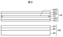
- FIG. 2 is a cross-sectional view of the liquid crystal display device.
- the backlight 20 is arranged on the back surface of the liquid crystal display panel 10.
- the liquid crystal display panel 10 has the following configuration. That is, the facing substrate 200 on which the black matrix and the color filter are formed is arranged so as to face the TFT substrate 100 on which the pixel electrodes, common electrodes, TFTs, scanning lines, video signal lines and the like are formed.
- the TFT substrate 100 and the facing substrate 200 are adhered to each other by a sealing material 16 at the periphery, and a liquid crystal 300 is enclosed inside.
- the liquid crystal molecules are initially oriented by the alignment film formed on the TFT substrate 100 and the facing substrate 200.
- the liquid crystal molecules rotate and form an image by controlling the light from the backlight 20 for each pixel. Since the liquid crystal 300 can control only the deflected light, the lower polarizing plate 101 is arranged under the TFT substrate 100, and only the deflected light is incident on the liquid crystal 300. The light modulated by the liquid crystal 300 is detected by the upper polarizing plate 201, and the image is visually recognized.
- the backlight 20 is arranged on the back surface of the liquid crystal display panel.
- the backlight 20 has a configuration in which the light guide plate 40 is arranged on the light source 30, and the optical sheet group 50 is arranged on the light guide plate 40.
- the backlight 20 of the display device includes a side light system in which a light source such as a light emitting diode (LED), which is a light emitting element, is arranged on the side surface of the light guide plate, and a direct type in which a light source such as an LED is arranged on the lower surface of the light guide plate.
- LED light emitting diode
- a direct type backlight is used.
- the light guide plate 40 is arranged on the light source 30.
- the light guide plate 40 is made of a transparent resin.
- the light guide plate 40 in FIG. 2 has a role of making the light from the LED, which is a point light source, uniform by reflecting the light incident on the light guide plate 40 at the interface.
- the optical sheet group 50 is arranged on the light guide plate 40.
- a prism sheet, a diffusion sheet, or the like is used for the optical sheet group 50.
- a color conversion sheet in which a phosphor is dispersed in a resin sheet or a color conversion sheet using quantum dots may be used.
- a deflection reflection sheet may be used. What kind of optical sheet is used or how many such optical sheets are used is determined by the display device.
- the bright part When displaying an image on a liquid crystal display device, the bright part transmits the backlight and the dark part shields the backlight.
- Image contrast is defined by the ratio of bright to dark areas.
- the dark portion is formed by shielding the light from the backlight by the liquid crystal.
- the shielding of the backlight by the liquid crystal is not perfect, and some light leaks. This will reduce the contrast.
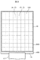
- FIG. 3 is an example of a liquid crystal display device showing a form of local dimming.
- FIG. 3 is a plan view of the liquid crystal display device, and the configuration is the same as that described with reference to FIG.
- the display area 14 is divided by segments 141.
- the dotted line in FIG. 3 is the boundary of the segment 141, but this is described for convenience, and the liquid crystal display panel does not have such a boundary.
- the light source in the backlight is arranged at the position corresponding to each segment.
- the segment (4, 2) is a bright part and the segment (5, 2) is a dark part.
- the light source of the segment (4, 2) portion that is, the LED is turned on
- the light source of the segment (5, 2) portion that is, the LED is not turned on.
- the black formed in the segment (5, 2) becomes a deep black display, and high contrast is realized.
- the light of the segment (4, 2) may reach the segment (5, 2). Then, the backlight is also illuminated on the segments (5, 2) that should be displayed in black, and the effect of local dimming cannot be fully exerted.
- FIGS. 4 and 5 are Comparative Example 1 showing the configuration of the backlight that enables local dimming.
- a blue LED 60 is used as a light source.
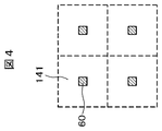
- FIG. 4 is a plan view showing the arrangement of the LED 60, which is a light source, in each segment 141 of the backlight.
- each segment 141 is partitioned by a dotted line. However, this dotted line is for convenience only and does not actually have a partition.
- the size of each segment is 4 mm ⁇ or less, and in the case of FIG. 5, it is, for example, 2 mm ⁇ .
- the size of the segment 141 in the following example is also the same.
- one LED 60 is arranged in each segment 141.
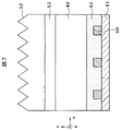
- FIG. 5 is a cross-sectional view of the backlight in Comparative Example 1.
- the LED 60 is arranged on the light source substrate 61, and the transparent resin 62 is formed so as to cover the LED 60.
- a blue LED is used for the LED 60.
- the transparent resin 62 for example, an acrylic resin or a silicone resin is used.
- the transparent resin 62 is for protecting the electrodes and wiring formed on the LED 60 and the light source substrate 61.
- the dotted line shown on the light source substrate 61 in FIG. 5 indicates the boundary of the segment for convenience.
- the light guide plate 40 is arranged on the transparent resin 62. Although the light guide plate 40 is transparent, it has a function of reflecting the light incident on the light guide plate 40 at the interface and making the light from the LED 60 uniform.
- the color conversion sheet 51 is arranged on the light guide plate 40.
- the color conversion sheet 51 is a transparent resin sheet in which a phosphor that receives blue light and develops yellow light is dispersed, and the light that has passed through the color conversion sheet 51 is white light.
- the thickness of the color conversion sheet 51 is, for example, 50 ⁇ m to 200 ⁇ m.
- a diffusion sheet 53 is arranged on the color conversion sheet 51.
- the diffusion sheet 53 is for diffusing the light from the light source 60 to make the brightness uniform.
- the thickness of the diffusion sheet 53 is, for example, 50 ⁇ m to 200 ⁇ m.
- a prism sheet 52 is arranged on the diffusion sheet 53.
- the prism sheet 52 is formed by extending prisms having a triangular cross section in the y direction and arranging them in the x direction.
- the role of the prism sheet 52 is to improve the efficiency of light utilization by directing the light emitted obliquely from the main surface of the color conversion sheet 51 in the direction perpendicular to the main surface of the color conversion sheet 51. In FIG.
- the number of prism sheets 52 is one, but a prism sheet having a prism array extending in a direction perpendicular to the prism array of the prism sheet 52 in FIG. 5 may be added.
- the thickness of the prism sheet is, for example, 50 microns in the portion of the prism array (that is, the height of the prism) and 70 microns in the thickness of the base material portion, which is about 120 microns in total.
- FIG. 6 and 7 are comparative examples 2 when a white LED 65 is used as a light source.
- FIG. 6 is the same as FIG. 4 except that the LED as a light source is a white LED 65.
- FIG. 7 is a cross-sectional view of the backlight in Comparative Example 2.
- the white LED 65 is arranged on the light source substrate 61, and the transparent resin 62 is formed so as to cover the white LED 65.
- the light guide plate 40 is arranged on the transparent resin 62.
- the role of the light guide plate 40 is the same as that described in Comparative Example 1.
- the diffusion sheet 53 exists on the light guide plate 40, and the color conversion sheet 51 does not exist. This is because the white LED 65 is used, so there is no need for color conversion.
- the role of the diffusion sheet 53 is the same as described in FIG.
- the prism sheet 52 is arranged on the diffusion sheet 53. The structure and operation of the prism sheet are the same as those described in FIG.
- Comparative Examples 1 and 2 The problem of Comparative Examples 1 and 2 is that the light from the LED 60 or 65 leaks from the transparent resin 62 covering the LEDs 60 and 65, the light guide plate 40, the color conversion sheet 51 and the diffusion sheet 53 to the adjacent segments. be. In particular, light leakage to the adjacent segment via the transparent resin 62, which is close to the light source, is large.
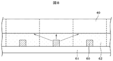
- FIG. 8 is a cross-sectional view showing the problems of Comparative Examples 1 and 2.
- the LED 60 is arranged on the light source substrate 61, and the transparent resin 62 is formed so as to cover the LED 60.
- a light guide plate 40 is arranged on the transparent resin 62.
- the optical sheet group above the light guide plate 40 is omitted.
- the dotted line in FIG. 8 indicates the boundary of the segment, but this is for convenience only, and such a line does not actually exist.
- the arrow in FIG. 8 indicates the traveling direction of light.
- the light from the LED 60 is emitted not only in the upward direction but also in the lateral direction or the diagonal direction.
- the light emitted obliquely from the LED 60 is incident on the adjacent segment. Even when black is displayed in the adjacent segment, this light is emitted to the display panel, and effective local dimming cannot be performed.
- FIG. 9 is a cross-sectional view showing the configuration and operation in this embodiment.
- the configuration of FIG. 9 is the same as that of FIG. 8 except that the transparent resin 62 is divided by the groove-shaped gap 70 at the boundary of the segment.
- the arrow in FIG. 9 indicates the emission direction of the light from the LED 60.
- the light emitted obliquely from the LED 60 is reflected by the groove-shaped gap 70 of the transparent resin 60, and the significantly reduced light is incident on the adjacent segment. That is, light is reflected at the interface between the transparent resin 62 and the groove-shaped gap 70 due to the difference in the refractive index between the transparent resin 62 and the air.
- the influence of light leakage on local dimming can be kept small.
- the refractive index of the transparent resin 62 the better.
- the material of the transparent resin 62 for example, an acrylic resin, a silicone resin, or the like can be used.
- the plane of the LED 60 is rectangular, for example, a square, and the width lx of the LED 60 is 0.1 mm to 0.5 mm.
- the thickness rt of the transparent resin is, for example, 0.5 mm to 1 mm.
- the height lh of the LED 60 is, for example, 0.3 mm to 0.5 mm.
- the width gw of the groove-shaped gap 70 has a relatively large degree of freedom, but it is better that it is as small as possible. That is, since the light from the LED 60 does not reach the groove-shaped gap 70, the portion of the groove-shaped gap 70 becomes dark, and when observed on the surface of the transparent resin 62, the brightness becomes uneven. However, normally, the influence of the groove-shaped gap 70 is scattered by the effect of the light guide plate 40, the diffusion sheet 53, etc. arranged on the transparent resin 62, and the uneven brightness is not recognized on the screen of the display panel. However, the narrower the width gw of the groove-shaped gap 70 is, the less likely it is that uneven brightness will occur.
- FIG. 10 is a cross-sectional view showing the process of forming the transparent resin 62 in FIG.
- the transparent resin 62 is processed by photolithography.
- the transparent resin 62 is made of a positive photosensitive resin.
- the photosensitive resin 62 is applied over the LED 60 on the light source substrate 61 and temporarily cured. Then, using the exposure mask 400, only the portion 621 corresponding to the groove-shaped gap 70 is exposed and developed. After that, it may be finally cured.
- FIG. 11 is a plan view of the light source substrate 61 formed in this way.
- a groove 70 is formed in the photosensitive resin 62 along the boundary of the segment 141, and the LED 60 is arranged in the central portion of the segment 141.
- the size of each segment 141 is 4 mm ⁇ or less, for example, 2 mm ⁇ .
- FIG. 12 is a cross-sectional view of a backlight according to the present invention using the light source substrate 61 shown in FIG.
- the area above the light guide plate 40 is the same as that in FIG. 5, which is Comparative Example 1.
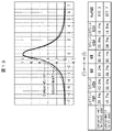
- the transparent resin 62 covering the LED 60 has a groove-shaped gap 70 formed at the boundary of the segments. Therefore, as described with reference to FIG. 9, light leakage to the adjacent segment through the transparent resin 62 can be reduced.
- FIG. 13 is a graph comparing light leakage to adjacent segments between Example 1 and Comparative Example 1.
- the data in the upper graph and the lower table in FIG. 13 are the same.
- the horizontal axis is the distance from the central portion of the specific segment in which the LED is arranged, and the unit is the diameter of the segment (lx in FIG. 9).
- the vertical axis is the relative brightness. That is, it is the relative brightness when the brightness in the central portion of the LED is 1.
- the brightness is measured above the prism sheets of FIGS. 5 (Comparative Example 1) and FIG. 12 (Example 1).
- the full lighting brightness in the table of FIG. 13 is the brightness when the full screen is displayed in white. In this case, it is almost the same in Example 1 and Comparative Example.
- the total lighting brightness is increased by about 1%, which is considered to be because the amount of light escaping to the outside of the screen when viewed in a plane is small in the segment around the screen. Can be done.
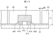
- FIG. 14 is a detailed cross-sectional view showing an LED 60, a transparent resin 62, a groove-shaped gap 70, and the like.
- the LED 60 is a blue LED.
- the light source substrate 61 is made of, for example, an epoxy resin.
- an electrode pad 612 connected to the anode 601 of the LED 60 and an electrode pad 613 connected to the cathode 602 of the LED 60 are formed of metal.
- Various other wirings are formed on the light source substrate 61, but they are omitted in FIG.
- the LED 60 is flip-chip bonded to the electrode pads 612 and 613 of the light source substrate 61.
- the LED 60 is formed by joining a p-type semiconductor and an n-type semiconductor, but in reality, various layers are formed in order to increase the luminous efficiency.
- the LED 60 is covered with a transparent resin 62 and protected.
- a voltage is applied to the LED 60, it emits light at the boundary between the p-type layer and the n-type layer.
- the light from the LED 60 is emitted not only in the upward direction but also in the lateral direction.
- the light emitted in the lateral direction enters the adjacent segment and adversely affects the local dimming operation. Therefore, as described with reference to FIG. 9, a groove-shaped gap 70 is formed to reflect light and reduce light leakage to adjacent pixels.
- the electrodes 612, 613 and the like are not protected by the transparent resin 62 and are exposed to the outside air. If a corrosive material is used for the electrode material, there is a risk of disconnection of the electrode. Further, since the thickness of the transparent resin 62 is relatively thick, about 0.5 mm to 1 mm, it may be difficult to reduce the width gw of the groove-shaped gap 70.
- the light emission of the LED 60 is performed at the junction between the p-type semiconductor and the n-type semiconductor. Therefore, even if the groove-shaped gap 70 is not formed up to the bottom of the LED 60, the light shielding effect from the LED 60 may be obtained. In such a case, the groove-shaped gap 70 may not be formed to a depth reaching the surface of the electrode or the light source substrate, and may be stopped in the middle.
- FIG. 15 is a cross-sectional view showing this example.
- the depth gd of the grooved gap 70 is larger than half the thickness rt of the transparent resin 62, but smaller than the thickness rt of the transparent resin 62.
- the depth of the groove-shaped gap 70 can be set to a value larger than the distance between the joint portion between the p-type semiconductor and the n-type semiconductor and the surface of the transparent resin 62, and smaller than the thickness rt of the transparent resin 62. ..
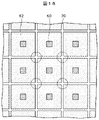
- FIG. 16 is a plan view showing a state in which the LED 60 and the transparent resin 62 are formed on the light source substrate and the groove-shaped gap 70 is formed in the transparent resin 62. As shown in FIG. 16, in the corner portion, the influence of the groove-shaped gap 70 on the brightness is most likely to be exerted.
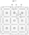
- FIG. 17 is a plan view showing the shape of the groove-shaped gap 70 formed in the transparent resin 62 to prevent this uneven brightness.
- the groove-shaped gap 70 is not formed in the portion corresponding to the corner portion of the segment. That is, if the groove-shaped gap 70 is not formed, the light from the LED 60 is not blocked, so that the brightness does not decrease. Further, since the corner portion of the segment has a large distance from the center of the LED 60, the amount of light leakage to the adjacent pixel through the corner is small. Therefore, even if the groove-shaped gap 70 is not formed in the corner portion, the effect of local dimming is not significantly impaired.
- the range in which the groove-shaped gap 70 is omitted is determined by the balance between the uneven brightness when the all-white display is displayed and the effect of local dimming. That is, the range in which the groove-shaped gap 70 is formed is determined within the range in which the luminance unevenness does not occur in the all-white display. For example, assuming that the range in which the groove-shaped gap 70 is omitted at the corner is s, in the experiment, s is preferably in the range of about 2 to 6 times the width gw of the groove-shaped gap 70.
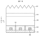
- FIG. 18 is a cross-sectional view showing a backlight according to the present invention when a white LED 65 is used.
- the light source portion of FIG. 18 merely changes the blue LED 60 in FIG. 12 of the first embodiment to a white LED 65.
- FIG. 18 there is no color conversion sheet in the optical sheet group. This is because the light source is white light, so there is no need for color conversion.
- Other configurations of FIG. 18 are the same as those of FIG.
- the detailed cross-sectional view of the light source substrate when the white LED 65 is used is the same as that of FIG. 14 or FIG. 15 in the first embodiment except that the blue LED 60 is replaced with the white LED. Further, the action and effect in these configurations are the same as those described in FIGS. 14 and 15 of Example 1. Further, the configuration described in the second embodiment can also be applied in the third embodiment.
- Examples 1 to 3 a case where one LED 60 as a light source is used per segment has been described.
- the present invention can be applied without any problem even when a plurality of LEDs 60 are formed per segment.
- the brightness of each LED 60 can be small, so that the problem that the bright spots due to the LEDs 60 are visible from the screen side is unlikely to occur. Therefore, it may be possible to remove the diffusion sheet 63 from the optical sheet group.
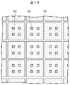
- FIG. 19 is a plan view when four LEDs 60 are used per segment.
- a groove-shaped gap 70 is formed along the boundary of each segment.
- Other configurations are the same as those in FIG. 11 of the first embodiment.
- the cross-sectional view is the same as that of FIG. 12 of the first embodiment except that there are a plurality of LEDs.
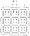
- FIG. 20 is a plan view showing an example in which four LEDs 60 are used per segment in the configuration of the second embodiment.
- FIG. 20 is the same as FIG. 17 of the second embodiment except that four LEDs 60 are present per segment.
- the light guide plate 40 is arranged on the transparent resin 62 that covers the LEDs 60 and 65, but the light guide plate 40 is not always necessary if there is no problem with uneven brightness or the like.
- the optical sheet group 50 is directly arranged on the transparent resin 62 that covers the LEDs 60 and 65.
Landscapes
- Physics & Mathematics (AREA)
- Nonlinear Science (AREA)
- Mathematical Physics (AREA)
- Chemical & Material Sciences (AREA)
- Crystallography & Structural Chemistry (AREA)
- General Physics & Mathematics (AREA)
- Optics & Photonics (AREA)
- Engineering & Computer Science (AREA)
- General Engineering & Computer Science (AREA)
- Liquid Crystal (AREA)
- Planar Illumination Modules (AREA)
- Devices For Indicating Variable Information By Combining Individual Elements (AREA)
Abstract
本発明の課題は、正確なローカルディミングによって、高精細で、コントラストの高い表示装置を実現することである。このために、本発明は、次のような構成をとる。表示パネル及びバックライトを有する表示装置であって、前記バックライトは光源と光学シート群を有し、前記光源は、光源基板61と前記光源基板61に配置したLED60を有し、前記光源は、平面で視てセグメントに分割され、前記セグメントには、少なくとも1個の前記LED60が存在し、前記光源基板61及び前記LED60は、透明樹脂62によって覆われ、前記透明樹脂62には、前記セグメントの境界に沿って溝状ギャップ70が形成されていることを特徴とする表示装置。
Description
本発明は、バックライトを有する表示装置に係り、特に、ローカルディミングを用いて高コントラスト画面を可能とする表示装置に関する。
液晶表示装置では画素電極および薄膜トランジスタ(TFT)等がマトリクス状に形成されたTFT基板と、TFT基板に対向して、対向基板が配置され、TFT基板と対向基板の間に液晶層が挟持されている。そして液晶分子による光の透過率を画素毎に制御することによって画像を形成している。
一方、有機EL表示装置では、有機EL層による発光素子、駆動TFT、スイッチングTFT等を有する画素がマトリクス状に形成され、画素毎に有機EL層の発光強度を制御して画像を形成している。有機EL表示装置は自発光素子なので、画像のコントラストが優れている。
しかし、画素の大きさは液晶表示装置のほうが小さくできるので、精細度は液晶表示装置のほうが優れている。そこで、液晶表示装置のコントラストを向上させる方式としてローカルディミングが開発されている。ローカルディミングに関する先行技術として、例えば特許文献1が存在する。
VR(Virtual Reality)用表示装置、医療用表示装置では、より高精細で、よりコントラストの高い画像が必要とされる。このような表示装置でローカルディミングを用いる場合、ローカルディミングについても、より細かい制御が必要である。
このような表示装置で、より効果的にローカルディミングを行い、コントラストを向上させるためには、例えば、ローカルディミングの単位となるセグメントの面積を小さくし、かつ、各セグメントの光が隣接するセグメントに及ばないようにする必要がある。
また、セグメントの面積を小さくすると、セグメントに複数のLEDを配置することが難しくなる。一方、各セグメントに1個のみLEDを配置した場合、輝度分布の均一化が問題となり、画面側からLEDが見えてしまうという問題を生ずる。これを対策するために、例えば、拡散シートを配置すると、拡散シートの影響によって、各セグメントの光が隣接するセグメントに漏れるという問題を生ずる。
本発明の課題は、このような問題を解決し、ローカルディミングを効果的に行い、バックライトを有する表示装置において、高精細で高コントラストの画面を実現することである。
本発明は上記課題を解決するものであり、主な具体的な手段は次のとおりである。
(1)表示パネル及びバックライトを有する表示装置であって、前記バックライトは光源と光学シート群を有し、前記光源は、光源基板と前記光源基板に配置したLEDを有し、前記光源は、平面で視てセグメントに分割され、前記セグメントには、少なくとも1個の前記LEDが存在し、前記光源基板及び前記LEDは、透明樹脂によって覆われ、前記透明樹脂には、前記セグメントの境界に沿って溝状ギャップが形成されていることを特徴とする表示装置。
(2)前記光学シート群と透明樹脂との間には、導光板が配置し、前記透明樹脂は前記導光板と接していることを特徴とする(1)に記載の表示装置。
(3)前記溝状ギャップは前記セグメントのコーナー部には形成されていないことを特徴とする(1)に記載の表示装置。
(4)前記溝状ギャップの深さは、前記透明樹脂の厚さよりも小さいことを特徴とする(1)に記載の表示装置。
以下に実施例を用いて本発明を詳細に説明する。
図1は液晶表示装置の1例を示す平面図である。図1において、TFT基板100と対向基板200がシール材16によって接着し、内部に液晶が挟持されている。TFT基板100と対向基板200がオーバーラップした部分に表示領域14が形成されている。表示領域14には、走査線11が横方向(x方向)に延在し、縦方向(y方向)に配列している。また、映像信号線12が縦方向に延在して横方向に配列している。走査線11と映像信号線12で囲まれた領域に画素13が形成されている。
図1において、TFT基板100が対向基板200とオーバーラップしていない部分は端子領域15となっている。端子領域15には、液晶表示パネルに電源や信号を供給するためにフレキシブル配線基板17が接続している。液晶表示パネルを駆動するドライバICはフレキシブル配線基板17に搭載されている。TFTの背面には、図2に示すようにバックライトが配置している。
図2は液晶表示装置の断面図である。図2において、液晶表示パネル10の背面にバックライト20が配置している。液晶表示パネル10は次のような構成になっている。すなわち、画素電極、コモン電極、TFT、走査線、映像信号線等が形成されたTFT基板100に対向して、ブラックマトリクスやカラーフィルタが形成された対向基板200が配置している。TFT基板100と対向基板200は周辺において、シール材16によって接着し、内部に液晶300が封入されている。
液晶分子は、TFT基板100及び対向基板200に形成された配向膜によって、初期配向している。画素電極とコモン電極の間に電圧が印加されると、液晶分子が回転し、画素毎にバックライト20からの光を制御することによって画像を形成する。液晶300は、偏向光のみ制御することが出来るので、TFT基板100の下に下偏光板101を配置して、偏向光のみを液晶300に入射する。液晶300で変調された光は、上偏光板201において、検光され、画像が視認される。
図2において、液晶表示パネルの背面にバックライト20が配置している。バックライト20は光源30の上に導光板40が配置し、その上に光学シート群50が配置している構成である。表示装置のバックライト20には、発光素子である発光ダイオード(LED)等の光源が導光板の側面に配置するサイドライト方式と、LED等の光源が導光板の下面に配置する直下型とが存在するが、本発明では、直下型方式のバックライトを使用する。
図2において、光源30の上には導光板40が配置している。導光板40は透明な樹脂で形成されている。図2における導光板40は、導光板40に入射した光を界面において反射させることによって、点光源であるLEDからの光を均一化させる役割を有する。
導光板40の上には光学シート群50が配置している。光学シート群50には、プリズムシート、拡散シート等が用いられる。この他に、光源に青色LED等を用いて白色光を得るために、樹脂シート内に蛍光体を分散した色変換シートや、量子ドットを使用した色変換シートが用いられることもある。また、バックライト20からの光の利用効率を向上させるために、偏向反射シートが用いられることもある。どのような光学シートを用いるか、あるいは、このような光学シートを何枚用いるかは表示装置によって決められる。
液晶表示装置に画像を表示する場合、明るい部分はバックライトを透過し、暗い部分は、バックライトを遮蔽する。画像のコントラストは、明るい部分と暗い部分の比によって定義される。液晶表示装置は、暗い部分は、液晶によってバックライトからの光を遮蔽することによって形成する。しかし、液晶によるバックライトの遮蔽は、完全ではなく、若干の光が漏れる。これによってコントラストが低下することになる。
ローカルディミングは、暗い部分には、バックライトを照射しないことによって、深い黒表示を可能とする。したがって、高いコントラストを実現することが出来る。図3はローカルディミングの形態を示す液晶表示装置の例である。図3は液晶表示装置の平面図であり、構成は図1で説明したのと同様である。図3において、表示領域14はセグメント141によって分割されている。図3における点線は、セグメント141の境界であるが、これは便宜上記載したものであり、液晶表示パネルにこのような境界があるわけではない。バックライトにおける光源が各セグメントに対応する位置に配置されている。
図3において、セグメント(4、2)は明るい部分であり、セグメント(5、2)は暗い部分であるとする。ローカルディミングでは、セグメント(4、2)の部分の光源、すなわち、LEDを点灯し、セグメント(5、2)の部分の光源、すなわち、LEDは点灯しない。そうすると、セグメント(5、2)の部分に形成される黒は、深い黒表示となり、高いコントラストが実現される。
しかし、セグメント間には境界があるわけではないので、例えばセグメントの輝度分布等によっては、セグメント(4、2)の光がセグメント(5、2)に及ぶ場合がある。そうすると、黒表示をするはずのセグメント(5、2)にもバックライトが照射されることになり、ローカルディミングの効果を十分に発揮できないことになる。
図4及び図5は、ローカルディミングを可能とするバックライトの構成を示す比較例1である。図4及び図5では、光源として青色LED60が使用されている。図4は、バックライトにおいて、各セグメント141における、光源であるLED60の配置を示す平面図である。図4において、各セグメント141は点線で仕切られている。しかし、この点線は、便宜上のものであり、実際に仕切りがあるわけではない。各セグメントの大きさは4mm□以下であり、図5の場合は、例えば2mm□である。以下の例におけるセグメント141の大きさも同様である。図4において、各セグメント141に1個のLED60が配置している。
図5は、比較例1におけるバックライトの断面図である。図5において、光源基板61の上にLED60が配置し、LED60を覆って透明樹脂62が形成されている。LED60には青色LEDが使用されている。透明樹脂62には、例えばアクリル樹脂あるいはシリコーン樹脂が使用される。透明樹脂62は、LED60、及び光源基板61に形成された電極及び配線を保護するためのものである。図5の光源基板61に記載された点線は、便宜上セグメントの境界を示すものである。
透明樹脂62の上に導光板40が配置している。導光板40は、透明であるが、導光板40に入射した光を界面において反射し、LED60からの光を均一化する働きを有する。導光板40の上に色変換シート51が配置している。色変換シート51は、透明樹脂シートに青色光を受けて黄色光を発色する蛍光体を分散させたものであり、色変換シート51を通過した光は、白色光となっている。色変換シート51の厚さは例えば50μm乃至200μmである。
色変換シート51の上には拡散シート53が配置している。拡散シート53は、光源60からの光を拡散して輝度を均一化するためのものである。拡散シート53の厚さは、例えば、50μm乃至200μmである。拡散シート53の上にはプリズムシート52が配置している。プリズムシート52は、断面が3角形状のプリズムがy方向に延在し、x方向に配列したものである。プリズムシート52の役割は、色変換シート51の主面から斜め方向に出射した光を、色変換シート51の主面と直角方向に向けることによって、光の利用効率を高めることである。図5では、プリズムシート52は、1枚であるが、図5のプリズムシート52のプリズムアレイと直角方向に延在するプリズムアレイを有するプリズムシートを加える場合もある。プリズムシートの厚さは、例えば、プリズムアレイの部分の厚さ(すなわち、プリズムの高さ)が50ミクロン、基材の部分の厚さが70ミクロンであり、合計120ミクロン程度である。
図6及び図7は、光源として白色LED65を使用した場合の比較例2である。図6は、光源であるLEDが白色LED65である他は図4と同じである。図7は、比較例2におけるバックライトの断面図である。図7において、光源基板61の上に白色LED65が配置し、白色LED65を覆って透明樹脂62が形成されている。
透明樹脂62の上に導光板40が配置している。導光板40の役割は比較例1で説明したのと同様である。導光板40の上に拡散シート53が存在しており、色変換シート51は存在していない。白色LED65を使用しているので、色変換の必要が無いからである。拡散シート53の役割は図5で説明したのと同じである。拡散シート53の上にプリズムシート52が配置している。プリズムシートの構成及び作用は図5で説明したのと同じである。
比較例1及び2の問題点は、LED60または65からの光が、LED60、65を覆う透明樹脂62、導光板40、色変換シート51及び拡散シート53から隣接するセグメントに漏れてしまうということである。特に、光源に近い、透明樹脂62を介しての隣接セグメントへの光漏れが大きい。
図8は、比較例1、2の問題点を示す断面図である。図8において、光源基板61の上にLED60が配置し、LED60を覆って透明樹脂62が形成されている。透明樹脂62の上には導光板40が配置している。導光板40より上側の光学シート群は省略されている。図8の点線はセグメントの境界を示すものであるが、これは便宜上のもので、実際にはこのような線が存在しているわけではない。
図8における矢印は光の進行方向を示す。LED60からの光は上方向のみでなく、横方向あるいは斜め方向にも出射する。図8において、LED60から斜め方向に出射した光は、隣接したセグメントに入射する。隣接したセグメントにおいて黒表示する場合にも、この光が表示パネルに照射されることになり、効果的なローカルディミングが出来なくなる。
図9は、本実施例における構成と作用を示す断面図である。図9の構成は、セグメントの境界において透明樹脂62が溝状ギャップ70によって分断されている他は図8と同じである。図9の矢印はLED60からの光の出射方向を示す。図9において、LED60から斜め方向に出射した光は、透明樹脂60の溝状ギャップ70において反射し、隣接するセグメントには大幅に低減した光が入射する。つまり、透明樹脂62と空気との屈折率の差によって、透明樹脂62と溝状ギャップ70との界面において、光が反射されるからである。これによって、光漏れの、ローカルディミングへの影響は小さく抑えることが出来る。
したがって、透明樹脂62の屈折率は大きいほどよい。透明樹脂62の材料としては、たとえば、アクリル樹脂、シリコーン樹脂等を使用することが出来る。図9において、LED60の平面は矩形であり、例えば、正方形であり、LED60の幅lxは0.1mm乃至0.5mmである。透明樹脂の厚さrtは例えば0.5mm乃至1mmである。LED60の高さlhは例えば0.3mm乃至0.5mmである。
溝状ギャップ70の幅gwは、比較的大きな自由度をもっているが、加工できる範囲で小さいほうがよい。つまり、溝状ギャップ70にはLED60からの光が届かないので、溝状ギャップ70の部分は暗くなり、透明樹脂62の表面で観測した場合、輝度むらとなる。しかし、通常は、透明樹脂62の上に配置する導光板40、拡散シート53等の効果によって、溝状ギャップ70の影響は散らされ、表示パネルの画面では輝度むら認識されない。ただし、溝状ギャップ70の幅gwは狭いほうが輝度むらは生じにくいことに変わりはない。
図10は、図9における透明樹脂62を形成するプロセスを示す断面図である。図10では、透明樹脂62は、フォトリソグラフィで加工する。図10において、透明樹脂62の材料は、ポジ型の感光性樹脂を用いる。光源基板61の上にLED60を覆って感光性樹脂62を塗布し、仮硬化させる。その後、露光マスク400を用いて、溝状ギャップ70に対応する部分621のみに露光し、現像する。その後、本硬化させればよい。
図11は、このようにして形成された光源基板61の平面図である。セグメント141の境界に沿って感光性樹脂62に溝状ギャップ70が形成されている、セグメント141の中央部分にはLED60が配置している。各セグメント141の大きさは4mm□以下であり、例えば2mm□である。
図12は、図11に示す光源基板61を用いた本発明によるバックライトの断面図である。図12において、導光板40から上側は比較例1である図5と同じである。図12において、LED60を覆う透明樹脂62には、セグメントの境界において溝状ギャップ70が形成されている。したがって、図9で説明したように、透明樹脂62を通しての隣接セグメントへの光漏れは軽減することが出来る。
図13は、隣接セグメントへの光漏れを実施例1と比較例1とで比較したグラフである。図13の上側のグラフと下側の表のデータは同じものである。図13のグラフにおいて、横軸は、LEDを配置した特定セグメントの中央部分からの距離であり、単位はセグメ
ントの径(図9におけるlx)である。縦軸は相対輝度である。すなわち、LEDの中心部分における輝度を1とした場合の相対輝度である。なお、輝度は、図5(比較例1)及び図12(実施例1)の各々のプリズムシートの上方で測定している。
ントの径(図9におけるlx)である。縦軸は相対輝度である。すなわち、LEDの中心部分における輝度を1とした場合の相対輝度である。なお、輝度は、図5(比較例1)及び図12(実施例1)の各々のプリズムシートの上方で測定している。
図13のグラフと図13の表を対応させると次のようになる。表における「境界」は、グラフの横軸の0.5または-0.5に対応し、表における「1セグメント先境界」は、グラフの横軸の1.5または-1.5に対応し、表における「2セグメント先境界」は、グラフの横軸の2.5または-2.5に対応する。
図13のグラフ及び表において、理論的には、輝度は、特定セグメント中央を挟んで対称になるはずであるが、実験誤差等によって、非対称になっている。しかし、傾向は読み取ることが出来る。図13のグラフにおいて、横軸のプラス方向における輝度と横軸の-方向の輝度の平均をとれば、より合理的な比較が可能になる。図13のグラフ及び表に示すように、実施例1では、比較例1に比較して隣接セグメントへの光漏れは軽減している。したがって、実施例1では、より正確なローカルディミングを行うことが出来る。
図13の表における全点灯輝度は、全画面白表示した場合の輝度である。この場合、実施例1と比較例ではほぼ同じである。なお、実施例1において、1%ほど全点灯輝度が大きくなっているが、これは、画面周辺のセグメントにおいて、平面で視て画面外側に逃げる光の量が実施例1では小さいためと考えることが出来る。
図14は、LED60、透明樹脂62、溝状ギャップ70等を示す詳細断面図である。LED60は、青色LEDである。図14において、光源基板61は、例えば、エポキシ樹脂で形成されている。光源基板61の上に、LED60の陽極601と接続する電極パッド612及びLED60の陰極602と接続する電極パッド613が金属で形成されている。光源基板61上には、この他に種々の配線が形成されているが、図14では省略されている。LED60は光源基板61の電極パッド612、613にフリップチップボンディングされている。LED60の端子電極601、602と光源基板61の電極パッド612、613を対向させて、半田615を介して接続している。LED60は、p型半導体とn型半導体が接合したものであるが、実際には発光効率を上げるために、さまざまな層が形成されている。
図14において、LED60は、透明樹脂62で覆われ、保護されている。LED60に電圧を印加すると、p型層とn型層の境界で発光する。LED60からの光は、上方向のみでなく、横方向にも出射する。横方向に出射した光は隣接セグメントに入射してローカルディミング動作に悪影響を及ぼす。そこで、図9で説明したように、溝状ギャップ70を形成して光を反射し、隣接画素への光漏れを軽減している。
ところで、図14に示すように、例えば電極612、613等は透明樹脂62によって保護されず、外気に露出された状態となっている。電極材料に腐食し易い材料を使用すると、電極の断線等の危険が生ずる。また、透明樹脂62の厚さは0.5mm乃至1mm程度と、比較的厚いので、溝状ギャップ70の幅gwを小さくすることが難しい場合がある。
一方、LED60の発光は、p型半導体とn型半導体が接合部分で行われる。したがって、LED60の底部まで、溝状ギャップ70を形成しなくとも、LED60からの光の遮蔽効果を得ることが出来る場合がある。このような場合、溝状ギャップ70を電極あるいは、光源基板の表面に達する深さまで形成せず、途中で止めてもよい。
図15はこの例を示す断面図である。図15において、溝状ギャップ70の深さgdは、透明樹脂62の厚さrtの半分よりも大きいが、透明樹脂62の厚さrtよりも小さい。あるいは、溝状ギャップ70の深さは、p型半導体とn型半導体の接合部分と透明樹脂62表面との距離よりも大きく、透明樹脂62の厚さrtよりも小さい値に設定することが出来る。
実施例1で説明したように、セグメントの境界に沿って溝状ギャップ70を形成した場合、図9で説明したように、隣接するセグメントへの光漏れを軽減することが出来る。一方、溝状ギャップ70の部分には、両側のセグメントにおけるLED60からの光が届きにくいために、透明樹脂62の直上で視た場合、溝状ギャップ70の部分は暗く見える。しかし、透明樹脂62の上に配置する導光板40や拡散シート63等の効果によって、この輝度むらは通常は見えない。
しかし、全画面を白表示した場合、図16において、丸で囲んだ部分、すなわち、セグメントのコーナー部分において、輝度が小さくなり、その結果、輝度むらを生ずる場合がある。図16は、光源基板の上にLED60、透明樹脂62が形成され、透明樹脂62に溝状ギャップ70が形成された状態を示す平面図である。図16に示すように、コーナー部では、溝状ギャップ70の輝度に対する影響が最も及び易い。
図17はこの輝度むらを対策する、透明樹脂62に形成する、溝状ギャップ70の形状を示す平面図である。図17に示すように、溝状ギャップ70は、セグメントのコーナー部に対応する部分には形成されていない。すなわち、溝状ギャップ70が形成されていなければ、LED60からの光は遮蔽されないので、輝度が低下することはない。また、セグメントのコーナー部は、LED60の中心からの距離が大きいので、コーナーを介しての隣接する画素への光漏れ量は小さい。したがってコーナー部に溝状ギャップ70を形成しなくとも、ローカルディミングの効果を大きく損なうことはない。
コーナー部において、溝状ギャップ70を省略する範囲は、全白表示をした時の輝度むらとローカルディミングの効果の兼ね合いで決める。つまり、全白表示における輝度むらを生じない範囲で溝状ギャップ70を形成する範囲を決めることになる。例えば、コーナーにおいて溝状ギャップ70を省略する範囲をsとすると、実験では、sは、溝状ギャップ70の幅gwの2倍乃至6倍程度の範囲がよい。
このように、実施例2の構成によれば、全白表示における輝度むらを生じないように、かつローカルディミングの効果を上げることが出来る。
実施例1及び2では、光源として青色LED60を使用した場合について説明した。しかし、本発明は、白色LED65を使用した場合についても適用することが出来る。図18は白色LED65を使用した場合における本発明によるバックライトを示す断面図である。図18の光源部分は、実施例1の図12における青色LED60を白色LED65に変えただけである。図18において、光学シート群には、色変換シートは存在していない。光源が白色光なので、色変換の必要が無いからである。図18のその他の構成は図12と同じである。
白色LED65を使用した場合の光源基板の詳細断面図は、青色LED60が白色LEDに替わる他は、実施例1における図14、あるいは、図15と同じである。また、これらの構成における作用効果も、実施例1の図14及び図15で説明したのと同じである。さらに、実施例2で説明した構成も、実施例3において、適用することが出来る。
実施例1乃至3では、光源であるLED60を1セグメント当たり1個使用する場合について説明した。しかし、本発明は、LED60は1セグメント当たり複数形成する場合も問題なく適用することが出来る。1セグメント当たり、複数のLED60が存在する場合は、個々のLED60の輝度は小さくてすむので、LED60による輝点が画面側から見えてしまうという問題は起こりにくい。したがって、光学シート群から拡散シート63を除去できる場合もある。
図19は、1セグメントあたり、4個のLED60を使用した場合の平面図である。図19において、各セグメントの境界に沿って溝状ギャップ70が形成されている。その他の構成は実施例1の図11と同様である。また、断面図は、LEDが複数ある他は、実施例1の図12と同じである。
図20は、実施例2の構成において、1セグメントあたり、4個のLED60を使用した場合の例を示す平面図である。図20は、LED60が1セグメント当たり4個存在している他は、実施例2の図17と同じである。
このように、LED60が1セグメントあたり複数存在する場合にも、本発明を適用することによってローカルディミングを効果的に行うことが出来る。また、溝状ギャップ70の形成範囲を制御することによって、輝度むらを防止しつつ、ローカルディミングを効果的に行うことが出来る。
以上の説明では、LED60、65を覆う透明樹脂62の上に導光板40を配置する構成となっているが、輝度むら等が問題なければ、導光板40は必ずしも必要はない。この場合、LED60、65を覆う透明樹脂62の上に直接光学シート群50が配置される構成となる。
10…表示パネル、 11…走査線、 12…映像信号線、 13…画素、 14…表示領域、 15…端子領域、 16…シール材、 17…フレキシブル配線基板、 20…バックライト、 30…光源、 40…導光板、 50…光学シート群、 60…青色LED、 61…光源基板、 62…透明樹脂、 65…白色LED、 70…溝状ギャップ、 100…TFT基板、 101…下偏光板、 200…対向基板、 201…上偏光板、 300…液晶、 400…露光マスク、 601…陽極、 602…陰極、 612…電極パッド、 613…電極パッド、 615…半田、 621…被露光領域
Claims (11)
- 表示パネル及びバックライトを有する表示装置であって、
前記バックライトは光源と光学シート群を有し、
前記光源は、光源基板と前記光源基板に配置したLEDを有し、
前記光源は、平面で視てセグメントに分割され、
前記セグメントには、少なくとも1個の前記LEDが存在し、
前記光源基板及び前記LEDは、透明樹脂によって覆われ、
前記透明樹脂には、前記セグメントの境界に沿って溝状ギャップが形成されていることを特徴とする表示装置。 - 前記光学シート群と透明樹脂との間には、導光板が配置し、前記透明樹脂は前記導光板と接していることを特徴とする請求項1に記載の表示装置。
- 前記溝状ギャップは前記セグメントのコーナー部には形成されていないことを特徴とする請求項1に記載の表示装置。
- 前記溝状ギャップの深さは、前記透明樹脂の厚さよりも小さいことを特徴とする請求項1に記載の表示装置。
- 前記溝状ギャップは空間であることを特徴とする請求項1に記載の表示装置。
- 前記LEDは青色LEDであり、前記光学シート群は色変換シートを含むことを特徴とする請求項1に記載の表示装置。
- 前記透明樹脂は感光性の樹脂で形成されていることを特徴とする請求項1に記載の表示装置。
- 前記セグメント内には、LEDが1個のみ存在し、前記光学シート群は拡散シートを含むことを特徴とする請求項1に記載の表示装置。
- 前記光学シート群は、プリズムシート、色変換シート、及び拡散シートを含むことを特徴とする請求項1に記載の表示装置。
- 前記バックライトはローカルディミング動作が可能であることを特徴とする請求項1乃至9のいずれか1項に記載の表示装置。
- 前記表示パネルは液晶表示パネルであることを特徴とする請求項1乃至9のいずれか1項に記載の表示装置。
Priority Applications (2)
| Application Number | Priority Date | Filing Date | Title |
|---|---|---|---|
| JP2022560649A JP7719094B2 (ja) | 2020-11-04 | 2021-08-11 | 表示装置および表示装置の製造方法 |
| US18/309,837 US12019330B2 (en) | 2020-11-04 | 2023-05-01 | Display device |
Applications Claiming Priority (2)
| Application Number | Priority Date | Filing Date | Title |
|---|---|---|---|
| JP2020-184172 | 2020-11-04 | ||
| JP2020184172 | 2020-11-04 |
Related Child Applications (1)
| Application Number | Title | Priority Date | Filing Date |
|---|---|---|---|
| US18/309,837 Continuation US12019330B2 (en) | 2020-11-04 | 2023-05-01 | Display device |
Publications (1)
| Publication Number | Publication Date |
|---|---|
| WO2022097339A1 true WO2022097339A1 (ja) | 2022-05-12 |
Family
ID=81457662
Family Applications (1)
| Application Number | Title | Priority Date | Filing Date |
|---|---|---|---|
| PCT/JP2021/029596 Ceased WO2022097339A1 (ja) | 2020-11-04 | 2021-08-11 | 表示装置 |
Country Status (3)
| Country | Link |
|---|---|
| US (1) | US12019330B2 (ja) |
| JP (1) | JP7719094B2 (ja) |
| WO (1) | WO2022097339A1 (ja) |
Families Citing this family (2)
| Publication number | Priority date | Publication date | Assignee | Title |
|---|---|---|---|---|
| GB2597100B (en) * | 2020-07-15 | 2024-01-31 | Design Led Products Ltd | Pixelated lighting device |
| WO2026058990A1 (ko) * | 2024-09-13 | 2026-03-19 | 엘지전자 주식회사 | 평면 조명 장치 |
Citations (4)
| Publication number | Priority date | Publication date | Assignee | Title |
|---|---|---|---|---|
| JP2018106826A (ja) * | 2016-12-22 | 2018-07-05 | オムロン株式会社 | 導光板、面光源装置、表示装置及び電子機器 |
| US20190094616A1 (en) * | 2017-09-28 | 2019-03-28 | Lg Display Co., Ltd. | Backlight unit and liquid crystal display device including the same |
| CN110806659A (zh) * | 2019-11-21 | 2020-02-18 | 业成科技(成都)有限公司 | 背光模组、其制作方法及显示装置 |
| CN111509105A (zh) * | 2019-08-30 | 2020-08-07 | 达运精密工业股份有限公司 | 发光元件、发光模块以及背光模块 |
Family Cites Families (7)
| Publication number | Priority date | Publication date | Assignee | Title |
|---|---|---|---|---|
| GB2438440B (en) * | 2006-05-26 | 2008-04-23 | Design Led Products Ltd | A composite light guiding device |
| TWI368792B (en) * | 2007-11-09 | 2012-07-21 | Au Optronics Corp | Lcd device, backlight module, thereof, with partition wall and method for manufacturing the same |
| JP2010135204A (ja) * | 2008-12-05 | 2010-06-17 | Citizen Electronics Co Ltd | 面状光源及び液晶表示装置 |
| US20120300135A1 (en) * | 2010-01-04 | 2012-11-29 | Sharp Kabushiki Kaisha | Lighting device, display device and television receiver |
| US9735198B2 (en) * | 2012-03-30 | 2017-08-15 | Cree, Inc. | Substrate based light emitter devices, components, and related methods |
| JP2017116683A (ja) | 2015-12-24 | 2017-06-29 | エルジー ディスプレイ カンパニー リミテッド | 液晶表示装置 |
| TWI739931B (zh) * | 2017-10-18 | 2021-09-21 | 優顯科技股份有限公司 | 顯示裝置 |
-
2021
- 2021-08-11 WO PCT/JP2021/029596 patent/WO2022097339A1/ja not_active Ceased
- 2021-08-11 JP JP2022560649A patent/JP7719094B2/ja active Active
-
2023
- 2023-05-01 US US18/309,837 patent/US12019330B2/en active Active
Patent Citations (4)
| Publication number | Priority date | Publication date | Assignee | Title |
|---|---|---|---|---|
| JP2018106826A (ja) * | 2016-12-22 | 2018-07-05 | オムロン株式会社 | 導光板、面光源装置、表示装置及び電子機器 |
| US20190094616A1 (en) * | 2017-09-28 | 2019-03-28 | Lg Display Co., Ltd. | Backlight unit and liquid crystal display device including the same |
| CN111509105A (zh) * | 2019-08-30 | 2020-08-07 | 达运精密工业股份有限公司 | 发光元件、发光模块以及背光模块 |
| CN110806659A (zh) * | 2019-11-21 | 2020-02-18 | 业成科技(成都)有限公司 | 背光模组、其制作方法及显示装置 |
Also Published As
| Publication number | Publication date |
|---|---|
| US12019330B2 (en) | 2024-06-25 |
| JPWO2022097339A1 (ja) | 2022-05-12 |
| JP7719094B2 (ja) | 2025-08-05 |
| US20230266620A1 (en) | 2023-08-24 |
Similar Documents
| Publication | Publication Date | Title |
|---|---|---|
| US20230341725A1 (en) | Display device | |
| US11003020B2 (en) | Light source package, backlight unit including light source package, and display device using the same | |
| KR102088872B1 (ko) | 백라이트 유닛 및 이를 구비한 액정표시장치 | |
| CN102819139B (zh) | 液晶显示装置 | |
| KR20110117579A (ko) | 액정표시장치 | |
| US12019330B2 (en) | Display device | |
| WO2022149359A1 (ja) | 表示装置 | |
| US12517397B2 (en) | Backlight and display device | |
| KR101827970B1 (ko) | 백라이트 유닛 및 그를 이용한 표시장치 | |
| US11392007B2 (en) | Display apparatus with a micro lite-emmitting diode panel overlapped with a reflective display panel | |
| CN108241235B (zh) | 光源模块及包括该光源模块的背光单元和液晶显示装置 | |
| KR20250023204A (ko) | 광 가이드 부재를 포함하는 유기 발광 표시 장치 | |
| US11852857B2 (en) | Display device | |
| JP2024036976A (ja) | 表示装置 | |
| JP2024054568A (ja) | 表示装置 | |
| US20250110370A1 (en) | Liquid crystal display device | |
| KR20110057710A (ko) | 백라이트 유닛 및 이를 구비한 액정표시장치 | |
| JP7737801B2 (ja) | 表示装置 | |
| JP2021162817A (ja) | 電子機器 | |
| KR20150125120A (ko) | 표시 장치 및 그 제조 방법 | |
| KR102678617B1 (ko) | 디스플레이 디바이스 | |
| US20250180801A1 (en) | Illumination device and display device | |
| JP2025126452A (ja) | 表示装置 | |
| JP2024106695A (ja) | バックライト及び表示装置 | |
| JP2024054567A (ja) | 表示装置 |
Legal Events
| Date | Code | Title | Description |
|---|---|---|---|
| 121 | Ep: the epo has been informed by wipo that ep was designated in this application |
Ref document number: 21888892 Country of ref document: EP Kind code of ref document: A1 |
|
| ENP | Entry into the national phase |
Ref document number: 2022560649 Country of ref document: JP Kind code of ref document: A |
|
| NENP | Non-entry into the national phase |
Ref country code: DE |
|
| 122 | Ep: pct application non-entry in european phase |
Ref document number: 21888892 Country of ref document: EP Kind code of ref document: A1 |