WO2022092129A1 - Wiring board, electronic device, and electronic module - Google Patents
Wiring board, electronic device, and electronic module Download PDFInfo
- Publication number
- WO2022092129A1 WO2022092129A1 PCT/JP2021/039572 JP2021039572W WO2022092129A1 WO 2022092129 A1 WO2022092129 A1 WO 2022092129A1 JP 2021039572 W JP2021039572 W JP 2021039572W WO 2022092129 A1 WO2022092129 A1 WO 2022092129A1
- Authority
- WO
- WIPO (PCT)
- Prior art keywords
- conductor
- wiring
- hole
- crystal grains
- wiring board
- Prior art date
Links
- 239000004020 conductor Substances 0.000 claims abstract description 151
- 239000010949 copper Substances 0.000 claims abstract description 87
- 239000013078 crystal Substances 0.000 claims abstract description 65
- 239000000758 substrate Substances 0.000 claims abstract description 25
- 229910052802 copper Inorganic materials 0.000 claims abstract description 9
- RYGMFSIKBFXOCR-UHFFFAOYSA-N Copper Chemical compound [Cu] RYGMFSIKBFXOCR-UHFFFAOYSA-N 0.000 claims abstract description 7
- 239000000470 constituent Substances 0.000 abstract 1
- 239000010410 layer Substances 0.000 description 24
- 239000010936 titanium Substances 0.000 description 14
- 238000004519 manufacturing process Methods 0.000 description 9
- 238000007747 plating Methods 0.000 description 9
- 239000000919 ceramic Substances 0.000 description 5
- 238000010304 firing Methods 0.000 description 5
- 239000007788 liquid Substances 0.000 description 5
- 238000001556 precipitation Methods 0.000 description 5
- 239000012141 concentrate Substances 0.000 description 4
- 238000000034 method Methods 0.000 description 4
- 229910052751 metal Inorganic materials 0.000 description 3
- 239000002184 metal Substances 0.000 description 3
- 150000002739 metals Chemical class 0.000 description 3
- 239000004065 semiconductor Substances 0.000 description 3
- 229910052719 titanium Inorganic materials 0.000 description 3
- GWEVSGVZZGPLCZ-UHFFFAOYSA-N Titan oxide Chemical compound O=[Ti]=O GWEVSGVZZGPLCZ-UHFFFAOYSA-N 0.000 description 2
- MCMNRKCIXSYSNV-UHFFFAOYSA-N Zirconium dioxide Chemical compound O=[Zr]=O MCMNRKCIXSYSNV-UHFFFAOYSA-N 0.000 description 2
- 238000005266 casting Methods 0.000 description 2
- 238000010586 diagram Methods 0.000 description 2
- 238000009713 electroplating Methods 0.000 description 2
- 239000007888 film coating Substances 0.000 description 2
- 238000009501 film coating Methods 0.000 description 2
- 229910052760 oxygen Inorganic materials 0.000 description 2
- 230000008646 thermal stress Effects 0.000 description 2
- OGIDPMRJRNCKJF-UHFFFAOYSA-N titanium oxide Inorganic materials [Ti]=O OGIDPMRJRNCKJF-UHFFFAOYSA-N 0.000 description 2
- 229910052581 Si3N4 Inorganic materials 0.000 description 1
- RTAQQCXQSZGOHL-UHFFFAOYSA-N Titanium Chemical compound [Ti] RTAQQCXQSZGOHL-UHFFFAOYSA-N 0.000 description 1
- 239000002253 acid Substances 0.000 description 1
- PNEYBMLMFCGWSK-UHFFFAOYSA-N aluminium oxide Inorganic materials [O-2].[O-2].[O-2].[Al+3].[Al+3] PNEYBMLMFCGWSK-UHFFFAOYSA-N 0.000 description 1
- QVGXLLKOCUKJST-UHFFFAOYSA-N atomic oxygen Chemical compound [O] QVGXLLKOCUKJST-UHFFFAOYSA-N 0.000 description 1
- 235000013405 beer Nutrition 0.000 description 1
- 238000005422 blasting Methods 0.000 description 1
- 229910000365 copper sulfate Inorganic materials 0.000 description 1
- PMHQVHHXPFUNSP-UHFFFAOYSA-M copper(1+);methylsulfanylmethane;bromide Chemical compound Br[Cu].CSC PMHQVHHXPFUNSP-UHFFFAOYSA-M 0.000 description 1
- ARUVKPQLZAKDPS-UHFFFAOYSA-L copper(II) sulfate Chemical compound [Cu+2].[O-][S+2]([O-])([O-])[O-] ARUVKPQLZAKDPS-UHFFFAOYSA-L 0.000 description 1
- 239000011229 interlayer Substances 0.000 description 1
- 150000002500 ions Chemical class 0.000 description 1
- 239000000463 material Substances 0.000 description 1
- 238000005259 measurement Methods 0.000 description 1
- 238000001000 micrograph Methods 0.000 description 1
- 230000003287 optical effect Effects 0.000 description 1
- 239000001301 oxygen Substances 0.000 description 1
- 230000002093 peripheral effect Effects 0.000 description 1
- 239000010970 precious metal Substances 0.000 description 1
- 238000004080 punching Methods 0.000 description 1
- HBMJWWWQQXIZIP-UHFFFAOYSA-N silicon carbide Chemical compound [Si+]#[C-] HBMJWWWQQXIZIP-UHFFFAOYSA-N 0.000 description 1
- 229910010271 silicon carbide Inorganic materials 0.000 description 1
- HQVNEWCFYHHQES-UHFFFAOYSA-N silicon nitride Chemical compound N12[Si]34N5[Si]62N3[Si]51N64 HQVNEWCFYHHQES-UHFFFAOYSA-N 0.000 description 1
- 238000005245 sintering Methods 0.000 description 1
- 229910000679 solder Inorganic materials 0.000 description 1
Images


Classifications
-
- H—ELECTRICITY
- H05—ELECTRIC TECHNIQUES NOT OTHERWISE PROVIDED FOR
- H05K—PRINTED CIRCUITS; CASINGS OR CONSTRUCTIONAL DETAILS OF ELECTRIC APPARATUS; MANUFACTURE OF ASSEMBLAGES OF ELECTRICAL COMPONENTS
- H05K1/00—Printed circuits
- H05K1/02—Details
- H05K1/11—Printed elements for providing electric connections to or between printed circuits
- H05K1/111—Pads for surface mounting, e.g. lay-out
- H05K1/112—Pads for surface mounting, e.g. lay-out directly combined with via connections
- H05K1/113—Via provided in pad; Pad over filled via
-
- H—ELECTRICITY
- H01—ELECTRIC ELEMENTS
- H01L—SEMICONDUCTOR DEVICES NOT COVERED BY CLASS H10
- H01L23/00—Details of semiconductor or other solid state devices
- H01L23/52—Arrangements for conducting electric current within the device in operation from one component to another, i.e. interconnections, e.g. wires, lead frames
- H01L23/522—Arrangements for conducting electric current within the device in operation from one component to another, i.e. interconnections, e.g. wires, lead frames including external interconnections consisting of a multilayer structure of conductive and insulating layers inseparably formed on the semiconductor body
- H01L23/532—Arrangements for conducting electric current within the device in operation from one component to another, i.e. interconnections, e.g. wires, lead frames including external interconnections consisting of a multilayer structure of conductive and insulating layers inseparably formed on the semiconductor body characterised by the materials
- H01L23/53204—Conductive materials
- H01L23/53209—Conductive materials based on metals, e.g. alloys, metal silicides
- H01L23/53228—Conductive materials based on metals, e.g. alloys, metal silicides the principal metal being copper
-
- H—ELECTRICITY
- H01—ELECTRIC ELEMENTS
- H01L—SEMICONDUCTOR DEVICES NOT COVERED BY CLASS H10
- H01L21/00—Processes or apparatus adapted for the manufacture or treatment of semiconductor or solid state devices or of parts thereof
- H01L21/02—Manufacture or treatment of semiconductor devices or of parts thereof
- H01L21/04—Manufacture or treatment of semiconductor devices or of parts thereof the devices having at least one potential-jump barrier or surface barrier, e.g. PN junction, depletion layer or carrier concentration layer
- H01L21/48—Manufacture or treatment of parts, e.g. containers, prior to assembly of the devices, using processes not provided for in a single one of the subgroups H01L21/06 - H01L21/326
- H01L21/4814—Conductive parts
- H01L21/4846—Leads on or in insulating or insulated substrates, e.g. metallisation
- H01L21/486—Via connections through the substrate with or without pins
-
- H—ELECTRICITY
- H01—ELECTRIC ELEMENTS
- H01L—SEMICONDUCTOR DEVICES NOT COVERED BY CLASS H10
- H01L23/00—Details of semiconductor or other solid state devices
- H01L23/12—Mountings, e.g. non-detachable insulating substrates
- H01L23/13—Mountings, e.g. non-detachable insulating substrates characterised by the shape
-
- H—ELECTRICITY
- H01—ELECTRIC ELEMENTS
- H01L—SEMICONDUCTOR DEVICES NOT COVERED BY CLASS H10
- H01L23/00—Details of semiconductor or other solid state devices
- H01L23/12—Mountings, e.g. non-detachable insulating substrates
- H01L23/14—Mountings, e.g. non-detachable insulating substrates characterised by the material or its electrical properties
- H01L23/15—Ceramic or glass substrates
-
- H—ELECTRICITY
- H01—ELECTRIC ELEMENTS
- H01L—SEMICONDUCTOR DEVICES NOT COVERED BY CLASS H10
- H01L23/00—Details of semiconductor or other solid state devices
- H01L23/48—Arrangements for conducting electric current to or from the solid state body in operation, e.g. leads, terminal arrangements ; Selection of materials therefor
- H01L23/488—Arrangements for conducting electric current to or from the solid state body in operation, e.g. leads, terminal arrangements ; Selection of materials therefor consisting of soldered or bonded constructions
- H01L23/498—Leads, i.e. metallisations or lead-frames on insulating substrates, e.g. chip carriers
- H01L23/49827—Via connections through the substrates, e.g. pins going through the substrate, coaxial cables
-
- H—ELECTRICITY
- H05—ELECTRIC TECHNIQUES NOT OTHERWISE PROVIDED FOR
- H05K—PRINTED CIRCUITS; CASINGS OR CONSTRUCTIONAL DETAILS OF ELECTRIC APPARATUS; MANUFACTURE OF ASSEMBLAGES OF ELECTRICAL COMPONENTS
- H05K1/00—Printed circuits
- H05K1/02—Details
- H05K1/09—Use of materials for the conductive, e.g. metallic pattern
-
- H—ELECTRICITY
- H05—ELECTRIC TECHNIQUES NOT OTHERWISE PROVIDED FOR
- H05K—PRINTED CIRCUITS; CASINGS OR CONSTRUCTIONAL DETAILS OF ELECTRIC APPARATUS; MANUFACTURE OF ASSEMBLAGES OF ELECTRICAL COMPONENTS
- H05K1/00—Printed circuits
- H05K1/02—Details
- H05K1/11—Printed elements for providing electric connections to or between printed circuits
- H05K1/115—Via connections; Lands around holes or via connections
-
- H—ELECTRICITY
- H05—ELECTRIC TECHNIQUES NOT OTHERWISE PROVIDED FOR
- H05K—PRINTED CIRCUITS; CASINGS OR CONSTRUCTIONAL DETAILS OF ELECTRIC APPARATUS; MANUFACTURE OF ASSEMBLAGES OF ELECTRICAL COMPONENTS
- H05K1/00—Printed circuits
- H05K1/02—Details
- H05K1/14—Structural association of two or more printed circuits
- H05K1/141—One or more single auxiliary printed circuits mounted on a main printed circuit, e.g. modules, adapters
-
- H—ELECTRICITY
- H05—ELECTRIC TECHNIQUES NOT OTHERWISE PROVIDED FOR
- H05K—PRINTED CIRCUITS; CASINGS OR CONSTRUCTIONAL DETAILS OF ELECTRIC APPARATUS; MANUFACTURE OF ASSEMBLAGES OF ELECTRICAL COMPONENTS
- H05K3/00—Apparatus or processes for manufacturing printed circuits
- H05K3/10—Apparatus or processes for manufacturing printed circuits in which conductive material is applied to the insulating support in such a manner as to form the desired conductive pattern
- H05K3/18—Apparatus or processes for manufacturing printed circuits in which conductive material is applied to the insulating support in such a manner as to form the desired conductive pattern using precipitation techniques to apply the conductive material
-
- H—ELECTRICITY
- H05—ELECTRIC TECHNIQUES NOT OTHERWISE PROVIDED FOR
- H05K—PRINTED CIRCUITS; CASINGS OR CONSTRUCTIONAL DETAILS OF ELECTRIC APPARATUS; MANUFACTURE OF ASSEMBLAGES OF ELECTRICAL COMPONENTS
- H05K3/00—Apparatus or processes for manufacturing printed circuits
- H05K3/40—Forming printed elements for providing electric connections to or between printed circuits
- H05K3/42—Plated through-holes or plated via connections
- H05K3/422—Plated through-holes or plated via connections characterised by electroless plating method; pretreatment therefor
-
- H—ELECTRICITY
- H05—ELECTRIC TECHNIQUES NOT OTHERWISE PROVIDED FOR
- H05K—PRINTED CIRCUITS; CASINGS OR CONSTRUCTIONAL DETAILS OF ELECTRIC APPARATUS; MANUFACTURE OF ASSEMBLAGES OF ELECTRICAL COMPONENTS
- H05K3/00—Apparatus or processes for manufacturing printed circuits
- H05K3/40—Forming printed elements for providing electric connections to or between printed circuits
- H05K3/42—Plated through-holes or plated via connections
- H05K3/423—Plated through-holes or plated via connections characterised by electroplating method
-
- H—ELECTRICITY
- H05—ELECTRIC TECHNIQUES NOT OTHERWISE PROVIDED FOR
- H05K—PRINTED CIRCUITS; CASINGS OR CONSTRUCTIONAL DETAILS OF ELECTRIC APPARATUS; MANUFACTURE OF ASSEMBLAGES OF ELECTRICAL COMPONENTS
- H05K3/00—Apparatus or processes for manufacturing printed circuits
- H05K3/40—Forming printed elements for providing electric connections to or between printed circuits
- H05K3/42—Plated through-holes or plated via connections
- H05K3/425—Plated through-holes or plated via connections characterised by the sequence of steps for plating the through-holes or via connections in relation to the conductive pattern
- H05K3/426—Plated through-holes or plated via connections characterised by the sequence of steps for plating the through-holes or via connections in relation to the conductive pattern initial plating of through-holes in substrates without metal
-
- H—ELECTRICITY
- H01—ELECTRIC ELEMENTS
- H01L—SEMICONDUCTOR DEVICES NOT COVERED BY CLASS H10
- H01L23/00—Details of semiconductor or other solid state devices
- H01L23/48—Arrangements for conducting electric current to or from the solid state body in operation, e.g. leads, terminal arrangements ; Selection of materials therefor
- H01L23/488—Arrangements for conducting electric current to or from the solid state body in operation, e.g. leads, terminal arrangements ; Selection of materials therefor consisting of soldered or bonded constructions
- H01L23/498—Leads, i.e. metallisations or lead-frames on insulating substrates, e.g. chip carriers
- H01L23/49866—Leads, i.e. metallisations or lead-frames on insulating substrates, e.g. chip carriers characterised by the materials
-
- H—ELECTRICITY
- H05—ELECTRIC TECHNIQUES NOT OTHERWISE PROVIDED FOR
- H05K—PRINTED CIRCUITS; CASINGS OR CONSTRUCTIONAL DETAILS OF ELECTRIC APPARATUS; MANUFACTURE OF ASSEMBLAGES OF ELECTRICAL COMPONENTS
- H05K1/00—Printed circuits
- H05K1/02—Details
- H05K1/03—Use of materials for the substrate
- H05K1/0306—Inorganic insulating substrates, e.g. ceramic, glass
-
- H—ELECTRICITY
- H05—ELECTRIC TECHNIQUES NOT OTHERWISE PROVIDED FOR
- H05K—PRINTED CIRCUITS; CASINGS OR CONSTRUCTIONAL DETAILS OF ELECTRIC APPARATUS; MANUFACTURE OF ASSEMBLAGES OF ELECTRICAL COMPONENTS
- H05K2201/00—Indexing scheme relating to printed circuits covered by H05K1/00
- H05K2201/09—Shape and layout
- H05K2201/09209—Shape and layout details of conductors
- H05K2201/095—Conductive through-holes or vias
- H05K2201/09563—Metal filled via
-
- H—ELECTRICITY
- H05—ELECTRIC TECHNIQUES NOT OTHERWISE PROVIDED FOR
- H05K—PRINTED CIRCUITS; CASINGS OR CONSTRUCTIONAL DETAILS OF ELECTRIC APPARATUS; MANUFACTURE OF ASSEMBLAGES OF ELECTRICAL COMPONENTS
- H05K2201/00—Indexing scheme relating to printed circuits covered by H05K1/00
- H05K2201/09—Shape and layout
- H05K2201/09818—Shape or layout details not covered by a single group of H05K2201/09009 - H05K2201/09809
- H05K2201/09827—Tapered, e.g. tapered hole, via or groove
-
- H—ELECTRICITY
- H05—ELECTRIC TECHNIQUES NOT OTHERWISE PROVIDED FOR
- H05K—PRINTED CIRCUITS; CASINGS OR CONSTRUCTIONAL DETAILS OF ELECTRIC APPARATUS; MANUFACTURE OF ASSEMBLAGES OF ELECTRICAL COMPONENTS
- H05K2201/00—Indexing scheme relating to printed circuits covered by H05K1/00
- H05K2201/10—Details of components or other objects attached to or integrated in a printed circuit board
- H05K2201/10227—Other objects, e.g. metallic pieces
- H05K2201/10378—Interposers
-
- H—ELECTRICITY
- H05—ELECTRIC TECHNIQUES NOT OTHERWISE PROVIDED FOR
- H05K—PRINTED CIRCUITS; CASINGS OR CONSTRUCTIONAL DETAILS OF ELECTRIC APPARATUS; MANUFACTURE OF ASSEMBLAGES OF ELECTRICAL COMPONENTS
- H05K2203/00—Indexing scheme relating to apparatus or processes for manufacturing printed circuits covered by H05K3/00
- H05K2203/07—Treatments involving liquids, e.g. plating, rinsing
- H05K2203/0703—Plating
- H05K2203/072—Electroless plating, e.g. finish plating or initial plating
-
- H—ELECTRICITY
- H05—ELECTRIC TECHNIQUES NOT OTHERWISE PROVIDED FOR
- H05K—PRINTED CIRCUITS; CASINGS OR CONSTRUCTIONAL DETAILS OF ELECTRIC APPARATUS; MANUFACTURE OF ASSEMBLAGES OF ELECTRICAL COMPONENTS
- H05K2203/00—Indexing scheme relating to apparatus or processes for manufacturing printed circuits covered by H05K3/00
- H05K2203/07—Treatments involving liquids, e.g. plating, rinsing
- H05K2203/0703—Plating
- H05K2203/0723—Electroplating, e.g. finish plating
-
- H—ELECTRICITY
- H05—ELECTRIC TECHNIQUES NOT OTHERWISE PROVIDED FOR
- H05K—PRINTED CIRCUITS; CASINGS OR CONSTRUCTIONAL DETAILS OF ELECTRIC APPARATUS; MANUFACTURE OF ASSEMBLAGES OF ELECTRICAL COMPONENTS
- H05K2203/00—Indexing scheme relating to apparatus or processes for manufacturing printed circuits covered by H05K3/00
- H05K2203/11—Treatments characterised by their effect, e.g. heating, cooling, roughening
- H05K2203/1126—Firing, i.e. heating a powder or paste above the melting temperature of at least one of its constituents
-
- H—ELECTRICITY
- H05—ELECTRIC TECHNIQUES NOT OTHERWISE PROVIDED FOR
- H05K—PRINTED CIRCUITS; CASINGS OR CONSTRUCTIONAL DETAILS OF ELECTRIC APPARATUS; MANUFACTURE OF ASSEMBLAGES OF ELECTRICAL COMPONENTS
- H05K2203/00—Indexing scheme relating to apparatus or processes for manufacturing printed circuits covered by H05K3/00
- H05K2203/11—Treatments characterised by their effect, e.g. heating, cooling, roughening
- H05K2203/1131—Sintering, i.e. fusing of metal particles to achieve or improve electrical conductivity
Definitions
- This disclosure relates to wiring boards, electronic devices and electronic modules.
- the wiring board according to the present disclosure is An insulating substrate having a first surface, a second surface opposite to the first surface, and a through hole extending from the first surface to the second surface.
- a wiring conductor located on the first surface and connected to the through conductor, Equipped with The through conductor and the wiring conductor contain copper as a main component and contain copper as a main component.
- the average size of Cu crystal grains in the through conductor is larger than the average size of Cu crystal grains in the wiring conductor.
- the electronic device according to this disclosure is With the above wiring board, Electronic components mounted on the wiring board and To prepare for.
- the electronic module according to this disclosure is With the above electronic devices The module board on which the electronic device is mounted and To prepare for.
- FIG. 1 It is a perspective view which shows the wiring board which concerns on embodiment of this disclosure. It is sectional drawing which shows the main part of the wiring board of FIG. It is a figure explaining the measuring method of the size of a Cu crystal grain. It is sectional drawing which shows the main part of the wiring board. It is a top view which shows the main part of the wiring board. It is explanatory drawing which shows an example of the manufacturing method of the wiring board which concerns on embodiment. It is a figure which shows the electronic apparatus and the electronic module which concerns on embodiment of this disclosure.
- FIG. 1 is a perspective view showing a wiring board according to an embodiment of the present disclosure.
- FIG. 2 is a cross-sectional view showing a main part of the wiring board of FIG.
- FIG. 2 shows a cross section of a portion of the wiring board 1 where the through conductor 25 is located.
- the wiring board 1 of the present embodiment includes an insulating substrate 10 having a first surface 11, a second surface 12 on the opposite side of the first surface 11, and a through hole 13 extending from the first surface 11 to the second surface 12. It includes a wiring conductor 21 located on the surface 11, a through conductor 25 located on the through hole 13 and the opening 13a of the through hole 13, and a wiring conductor 23 located on the second surface 12. The through conductor 25 is also located on the opening 13b on the second surface 12 side (opposite to the through hole 13). The through conductor 25 is connected to the wiring conductors 21 and 23.
- the insulating substrate 10 may be made of a ceramic containing aluminum nitride, silicon nitride, silicon carbide, alumina, zirconia, or the like as a main component.
- the through hole 13 has an opening 13a on the first surface 11 side and an opening 13b on the second surface 12 side, as shown by the alternate long and short dash line in FIG. Since the through conductor 25 is located in the through hole 13 and the openings 13a and 13b, the space is not open.
- the inner diameters of the openings 13a and 13b are larger than the inner diameter of the intermediate portion 13i of the through hole 13.
- the intermediate portion 13i means a flat surface portion in the through hole 13 parallel to the first surface 11 between the openings 13a and the openings 13b.
- the inner diameter of the through hole 13 may be gradually increased from the intermediate portion 13i to the opening 13a on the first surface 11 side.
- the inner diameter of the through hole 13 may be gradually increased from the intermediate portion 13i to the opening 13b on the second surface 12 side.
- the through hole 13 does not have to have a circular cross-sectional shape (cross-sectional shape parallel to the first surface 11), and if it is not circular, the above “inner diameter” may be read as "maximum width”.
- the wiring conductor 21 includes a main conductor portion 211 containing Cu (copper) as a main component, and an intermediate layer 212 located between the main conductor portion 211 and the first surface 11.
- the through conductor 25 includes a main conductor portion 251 containing Cu as a main component, and an intermediate layer 252 located between the main conductor portion 251 and the inner peripheral surface of the through hole 13.
- the wiring conductor 23 includes a main conductor portion 231 containing Cu as a main component, and an intermediate layer 232 located between the main conductor portion 231 and the second surface 12.
- the intermediate layers 212, 232 and 252 contain Cu, Ti (titanium) and O (oxygen).
- the main component means a component contained in an amount of 80% by mass or more.
- the main conductor portions 211 and 231 of the wiring conductors 21 and 23, and the main conductor portion 251 of the through conductor 25 are polycrystalline metals in which a plurality of Cu crystal grains t1 are gathered.
- Cu crystal grains t1 are schematically drawn.
- the actual Cu crystal grain t1 has various shapes such as granular and columnar, and has variations in size.
- the intermediate layers 212 and 232 of the wiring conductors 21 and 23 and the intermediate layer 252 of the through conductor 25 are polycrystalline metals in which a plurality of Cu crystal grains and a plurality of titanium oxide crystal grains are gathered.
- the sizes of the Cu crystal grains t1 of the wiring conductors 21 and 23, the Cu crystal grains t1 of the through conductor 25, and the Cu crystal grains of the intermediate layers 212, 232, and 252 will be described.
- the Cu crystal grains t1 of the wiring conductors 21 and 23 and the Cu crystal grains t1 of the through conductor 25 are simply referred to, they mean the Cu crystal grains t1 of the main conductor portions 211, 231 and 251.
- the size of Cu crystal grains is a size expressed in units of length.
- the wiring conductor 21 and the through conductor 25 are distinguished by the difference in the average size of the Cu crystal grains t1 and the difference in the average size.
- the average size of the Cu crystal grains t1 of the through conductor 25 is larger than the average size of the Cu crystal grains t1 of the wiring conductor 21.
- the difference in the average size of the Cu crystal grains t1 is a level difference that exceeds the error.
- the difference at a level exceeding the error may mean a difference of 1.5 times or more or 2 times or more of the standard deviation ⁇ of the size of the Cu crystal grain t1 measured at an arbitrary portion.
- Electromigration tends to occur around the opening 13a of the through hole 13 where the direction of the current changes and the current concentrates when the electric charge flows from the wiring conductor 21 to the through conductor 25.
- the Cu crystal grains t1 of the through conductor 25 is larger than the average size of the Cu crystal grains t1 of the wiring conductor 21, the Cu crystal grains t1 become difficult to move in the through conductor 25 and penetrate.
- the resistance to electromigration around the opening 13a of the hole 13 can be improved.
- the difference between the average size of the Cu crystal grains t1 of the through conductor 25 and the average size of the Cu crystal grains t1 of the wiring conductor 21 is 3 ⁇ m or less. With this configuration, the difference in size of the Cu crystal grains t1 at the boundary between the wiring conductor 21 and the through conductor 25 becomes small, so that the resistance to electromigration can be improved even at the boundary.
- the average size of the Cu crystal grains t1 of the through conductor 25 may be larger than the average size of the Cu crystal grains t1 of the wiring conductor 23 on the second surface 12 side.
- the difference in average magnitude is a level difference that exceeds the error and may be 3 ⁇ m or less.
- FIG. 3 is a diagram illustrating a method for measuring the size of Cu crystal grains.
- the Cu crystal grains t1 are simplified, and the number of Cu crystal grains t1 in the target region Rt is different from the actual number. 1.
- the SEM Sccanning Electron Microscope image or SIM (Scanning Ion Microscope) image
- the boundary (grain boundary) line of each Cu crystal grain t1 is extracted. 2.
- a region having a size including 20 to 100 Cu crystal grains t1 is arbitrarily selected as the target region Rt.
- the target region Rt is selected from a plurality of main portions of the conductor to be measured (main conductor portion 251 for the through conductor 25, main conductor portions 211 and 231 for the wiring conductors 21 and 23). 3.
- the number of Cu crystal grains t1 in each target region Rt is counted, and the area of each target region Rt is divided by the above number to calculate the average cross-sectional area of one Cu crystal grain t1. Further, assuming that the cross-sectional shape of each Cu crystal grain t1 is a circle, the diameter of the circle is calculated from the area, and the diameter is obtained as the average size of the Cu crystal grains t1.
- Example> When the average size of the Cu crystal grains t1 was measured for the through conductor 25 and the wiring conductor 21 for the wiring board 1 of the embodiment of the present disclosure, the result of the measurement result 1 was obtained.
- the result shows that the average size of the Cu crystal grains t1 of the through conductor 25 is larger than the average size of the Cu crystal grains t1 of the wiring conductor 21, and the difference between the two is 3 ⁇ m or less.
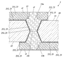
- FIG. 4A and 4B are views for explaining the boundary between the wiring conductor and the through conductor
- FIG. 4A is a cross-sectional view of a main part of the wiring board
- FIG. 4B is a plan view of the main part.
- the cross section of FIG. 4A is a cross section that passes through the through hole 13 and is perpendicular to the first surface 11.
- a large number of target regions Rt are set around the opening 13a of the through hole 13, the average size of Cu crystal grains t1 is measured for each target region Rt, and a boundary line in which the average size changes stepwise (FIG. By extracting (shown by a alternate long and short dash line in 4A), the boundary line can be specified as the boundary E1 between the through conductor 25 and the wiring conductor 21.
- the boundary E1 may be located outside the through hole 13 (that is, outside the opening 13a of the through hole 13) in the cross section of FIG. 4A. All of the boundaries E1 may be located outside the through holes 13. Electromigration tends to occur around the opening 13a of the through hole 13 in which the direction of the current changes and the current concentrates when the electric charge flows from the wiring conductor 21 to the through conductor 25. However, due to the configuration of the boundary E1 described above, the Cu crystal grains t1 of the through conductor 25 occupy the inside and outside of the opening 13a, so that the difference in size of the Cu crystal grains t1 between the inside and outside of the opening 13a becomes small. .. Therefore, the resistance to electromigration can be improved around the opening 13a of the through hole 13.
- the boundary E1 has the same tendency regardless of the orientation of the cross section (the orientation in the rotation direction about the central axis of the through hole 13). Therefore, when the wiring board 1 is seen through from the direction perpendicular to the first surface 11, the boundary E1 has a portion overlapping with the opening 13a of the through hole 13 of the insulating board 10, as shown in FIG. 4B. In the range having the above overlap, the difference in size of the Cu crystal grains t1 between the inside and the outside of the opening 13a becomes small. Therefore, with this configuration, the resistance to electromigration can be improved around the opening 13a of the through hole 13.
- the boundary E1 may overlap with the opening 13a in the entire circumferential direction of the opening 13a of the through hole 13. With this configuration, the resistance to electromigration can be improved over the entire circumferential direction of the opening 13a of the through hole 13.
- the boundary E1 includes the left first boundary line E1a and the right second boundary line E1b, and the distance between the first boundary line E1a and the second boundary line E1b penetrates.
- the distance from the hole 13 (opening 13a) may be narrower.
- the width of the through conductor 25 may be narrowed as it is separated from the through hole 13 (opening 13a).
- the angle between each portion of the boundary E1 and the line segment indicating the opening 13a may become smaller as it is closer to the edge of the opening 13a.
- the boundary E1 between the wiring conductor 23 and the through conductor 25 may be the same as the relationship between the boundary E1 on the first surface 11 side and the opening 13a in the relationship with the opening 13b on the second surface 12 side.
- the intermediate layers 212, 232, and 252 are polycrystalline metals containing at least Cu, Ti, and O, in which a plurality of Cu crystal grains and a plurality of titanium oxide crystal grains are gathered. Comparing the intermediate layer 252 of the through conductor 25 with the main conductor portion 251 of the through conductor 25, the average size of the Cu crystal grains is larger in the main conductor portion 251. Comparing the intermediate layers 212 and 232 of the wiring conductors 21 and 23 with the main conductor portions 211 and 231 of the wiring conductors 21 and 23, the average size of the Cu crystal grains is larger in the main conductor portions 211 and 231. ..
- the components of the intermediate layers 212 and 232 of the wiring conductors 21 and 23 and the intermediate layer 252 of the through conductor 25 and the average size of the Cu crystal grains may be substantially the same.
- FIG. 5 is a diagram illustrating an example of a method for manufacturing a wiring board according to an embodiment.
- the manufacturing method of the present embodiment includes a substrate forming step J1, a Ti film coating step J2, a firing step J3, a Cu plating and sinter step J4, an electrolytic plating step J5, and a resist peeling step J6 in chronological order.
- the ceramic green sheet which is a ceramic before sintering, is formed into a substrate shape by punching or die processing, and the substrate 70 before firing is formed.
- the substrate 70 is provided with a through hole 73 and a gutter 74 extending across the first surface 71 and the second surface 72 on the opposite side of the first surface 71.
- the diameter of the through hole 73 at an intermediate depth is larger than the diameter of the opening of the first surface 71 and the diameter of the opening of the second surface 72. Is also formed to be small.
- the substrate 70 becomes an insulating substrate 10 which is ceramic, and the through holes 73 and the gutters 74 of the substrate 70 before firing have the same shape as the through holes 13 and the gutters 14. It becomes.
- the through holes 13 and the gutters 14 may be formed by a method such as laser or blasting.
- the organic Ti liquid 81 is coated on the fired insulating substrate 10.
- the organic Ti liquid 81 is also applied to the inner wall surfaces of the through hole 73 and the gutter 74.
- the organic Ti liquid 81 may be applied to the first surface 71, the second surface 72, the inner wall surface of the through hole 73, and the inner wall surface of the gutter 74 with the same thickness.
- the organic Ti liquid 81 applied to the insulating substrate 10 is fired, so that the applied organic Ti liquid 81 becomes the oxidized Ti film 83.
- the Cu plating and sinter step J4 first, electroless Cu plating is applied on the Ti oxide film 83 on the surface of the insulating substrate 10, and then the sinter that diffuses the elements at the interface between the Ti oxide film 83 and the Cu plating film. Processing is done. By the sinter treatment, Cu is diffused in the Ti oxide film 83 to form the seed layer 85.
- the seed layer 85 corresponds to the intermediate layers 212, 232, and 252 in the wiring board 1 after the manufacturing process.
- the resist pattern 91 is formed so as to exclude the portions of the wiring conductors 21 and 23 and the through conductor 25, and electrolytic Cu plating is applied on the seed layer 85 not covered with the resist pattern 91.
- electrolytic Cu plating a Cu precipitation conductor 88 is formed on the seed layer 85, and the through holes 13 and the gutters 14 are filled with the Cu precipitation conductor 88.
- the Cu precipitation conductor 88 corresponds to the main conductor portions 211 and 231 of the wiring conductors 21 and 23, and the main conductor portion 251 of the through conductor 25.
- a through hole containing copper sulfate and a plating solution for beer filling (for example, VF-II manufactured by JCU Co., Ltd.) can be used.
- a Cu precipitation conductor is placed in a conductive rack, degreased, acid-treated, etc., then immersed in a plating solution and a current of about 0.5 to 3.0 A / dm 2 is applied. 88 is formed.
- the resist pattern 91 is removed, and the seed layer 85 not covered with the Cu precipitation conductor 88 is etched to manufacture the wiring board 1.
- the wiring board 1 it is possible to manufacture the wiring board 1 in which the average size of the Cu crystal grains t1 differs between the wiring conductors 21 and 23 and the through conductor 25 as described above.
- wiring conductors 21a and 21b and castings 25a and 25b are added to the configuration of FIG.
- FIG. 6 is a cross-sectional view showing an electronic device and an electronic module according to the embodiment of the present disclosure.
- the electronic device 60 is configured by mounting an electronic component 50 on a wiring board 1.
- the terminal of the electronic component 50 may be connected to the wiring conductor 21, and the terminal may be conducted to the wiring conductor 23 on the second surface 12 side via the wiring conductor 21 and the through conductor 25.
- a Ni film may be provided on the surfaces of the wiring conductors 21 and 23.
- Examples of the electronic component 50 include optical elements such as LD (LaserDiode), PD (PhotoDeode), LED (LightEmittingDiode), and image pickup elements such as CCD (ChargeCoupledDevice) type and CMOS (ComplementaryMetalOxideSemiconductor) type.
- Various electronic components such as piezoelectric vibrators such as crystal transducers, elastic surface wave elements, semiconductor elements such as semiconductor integrated circuit elements (ICs: Integrated Circuits), electric capacity elements, inductor elements, and resistors can be applied.
- the electronic module 100 is configured by mounting an electronic device 60 on a module board 110.
- other electronic devices, electronic elements, electric elements, and the like may be mounted on the module substrate 110.
- An electrode pad 111 may be provided on the module substrate 110, and the wiring conductor 23 of the electronic device 60 may be joined to the electrode pad 111 via a bonding material 113 such as solder.
- the reliability of the electronic device 60 and the electronic module 100 is improved by providing the wiring board 1 having improved resistance to electromigration around the opening 13a. Can be done.
- the wiring board, the electronic device, and the electronic module of the present disclosure are not limited to the above embodiment.
- the wiring conductor is exposed on the outer surface of the wiring board, and the through conductor is located between the two wiring conductors exposed on the outer surface of the wiring board.
- the wiring layer is located inside the substrate, and the through conductor may be an interlayer via of the multilayer wiring substrate.
- the through conductor may be a conductor constituting a through hole or a conductor constituting a casting.
- This disclosure can be used for wiring boards, electronic devices and electronic modules.
Abstract
Description
第1面と、前記第1面とは反対の第2面と、前記第1面から前記第2面にわたる貫通孔と、を有する絶縁基板と、
前記貫通孔内及び前記第1面側の前記貫通孔の開口上に位置する貫通導体と、
前記第1面に位置し前記貫通導体と繋がる配線導体と、
を備え、
前記貫通導体及び前記配線導体は主成分として銅を含み、
前記貫通導体におけるCu結晶粒の平均の大きさが、前記配線導体におけるCu結晶粒の平均の大きさよりも大きい。 The wiring board according to the present disclosure is
An insulating substrate having a first surface, a second surface opposite to the first surface, and a through hole extending from the first surface to the second surface.
A through conductor located in the through hole and above the opening of the through hole on the first surface side,
A wiring conductor located on the first surface and connected to the through conductor,
Equipped with
The through conductor and the wiring conductor contain copper as a main component and contain copper as a main component.
The average size of Cu crystal grains in the through conductor is larger than the average size of Cu crystal grains in the wiring conductor.
上記の配線基板と、
前記配線基板に搭載された電子部品と、
を備える。 The electronic device according to this disclosure is
With the above wiring board,
Electronic components mounted on the wiring board and
To prepare for.
上記の電子装置と、
前記電子装置が搭載されるモジュール用基板と、
を備える。 The electronic module according to this disclosure is
With the above electronic devices
The module board on which the electronic device is mounted and
To prepare for.
続いて、配線導体21、23のCu結晶粒t1、貫通導体25のCu結晶粒t1、中間層212、232、252のCu結晶粒の大きさについて説明する。以下、単に配線導体21、23のCu結晶粒t1、貫通導体25のCu結晶粒t1と言ったときには、主導体部211、231、251のCu結晶粒t1を意味するものとする。また、Cu結晶粒の大きさとは、長さの単位で表わされる大きさとする。 <Size of Cu crystal grains>
Subsequently, the sizes of the Cu crystal grains t1 of the
1.貫通導体25及び配線導体21を含む断面のSEM(Scanning Electron Microscope画像、又はSIM(Scanning Ion Microscope)画像において、各Cu結晶粒t1の境界(粒界)線を抽出する。
2.上記の画像から20個~100個のCu結晶粒t1が含まれる大きさの領域を、対象領域Rtとして任意に選ぶ。対象領域Rtは、計測対象の導体の主部(貫通導体25であれば主導体部251、配線導体21、23であれば主導体部211、231)から複数箇所選ぶ。
3.各対象領域Rt内のCu結晶粒t1の個数を計数し、各対象領域Rtの面積を上記個数で除算することで、1つのCu結晶粒t1の断面面積の平均を計算する。さらに、各Cu結晶粒t1の断面形状が円であるものと仮定し、上記面積から上記円の直径を計算し、当該直径をCu結晶粒t1の平均の大きさとして求める。 Since the Cu crystal grains t1 have various shapes such as granular and columnar, the average size of each Cu crystal grain t1 is determined by the following
1. 1. In the SEM (Scanning Electron Microscope image or SIM (Scanning Ion Microscope) image) of the cross section including the through
2. 2. From the above image, a region having a size including 20 to 100 Cu crystal grains t1 is arbitrarily selected as the target region Rt. The target region Rt is selected from a plurality of main portions of the conductor to be measured (main conductor portion 251 for the through
3. 3. The number of Cu crystal grains t1 in each target region Rt is counted, and the area of each target region Rt is divided by the above number to calculate the average cross-sectional area of one Cu crystal grain t1. Further, assuming that the cross-sectional shape of each Cu crystal grain t1 is a circle, the diameter of the circle is calculated from the area, and the diameter is obtained as the average size of the Cu crystal grains t1.
本開示の一実施例の配線基板1について貫通導体25と配線導体21とについてCu結晶粒t1の平均の大きさを計測すると、計測結果1の結果が得られた。

When the average size of the Cu crystal grains t1 was measured for the through
図4A及び図4Bは、配線導体と貫通導体との境界を説明する図であり、図4Aは配線基板の要部断面図、図4Bは当該要部の平面図である。図4Aの断面は、貫通孔13を通りかつ第1面11に垂直な断面である。 <Boundary between wiring conductor and through conductor>
4A and 4B are views for explaining the boundary between the wiring conductor and the through conductor, FIG. 4A is a cross-sectional view of a main part of the wiring board, and FIG. 4B is a plan view of the main part. The cross section of FIG. 4A is a cross section that passes through the through
中間層212、232、252は、先にも述べたように、少なくともCu、Ti、Oを含み、複数のCu結晶粒と複数のチタン酸化物の結晶粒とが集まった多結晶金属である。貫通導体25の中間層252と、貫通導体25の主導体部251とを比較すると、Cu結晶粒の平均の大きさは、主導体部251の方が大きい。配線導体21、23の中間層212、232と、配線導体21、23の主導体部211、231とを比較すると、Cu結晶粒の平均の大きさは、主導体部211、231の方が大きい。 <Middle layer>
As described above, the intermediate layers 212, 232, and 252 are polycrystalline metals containing at least Cu, Ti, and O, in which a plurality of Cu crystal grains and a plurality of titanium oxide crystal grains are gathered. Comparing the intermediate layer 252 of the through
図5は、実施形態に係る配線基板の製造方法の一例を説明する図である。 <Manufacturing method>
FIG. 5 is a diagram illustrating an example of a method for manufacturing a wiring board according to an embodiment.
図6は、本開示の実施形態に係る電子装置及び電子モジュールを示す断面図である。 <Electronic devices and electronic modules>
FIG. 6 is a cross-sectional view showing an electronic device and an electronic module according to the embodiment of the present disclosure.
10 絶縁基板
11 第1面
12 第2面
13 貫通孔
13a、13b 開口
13i 中間部
21、23 配線導体
25 貫通導体
211、231、251 主導体部
212、232、252 中間層
t1 Cu結晶粒
E1 境界
E1a 第1境界線
E1b 第2境界線
50 電子部品
60 電子装置
100 電子モジュール
110 モジュール用基板 1 Wiring
Claims (8)
- 第1面と、前記第1面とは反対の第2面と、前記第1面から前記第2面にわたる貫通孔と、を有する絶縁基板と、
前記貫通孔内及び前記第1面側の前記貫通孔の開口上に位置する貫通導体と、
前記第1面に位置し前記貫通導体と繋がる配線導体と、
を備え、
前記貫通導体及び前記配線導体は主成分として銅を含み、
前記貫通導体におけるCu結晶粒の平均の大きさが、前記配線導体におけるCu結晶粒の平均の大きさよりも大きい、
配線基板。 An insulating substrate having a first surface, a second surface opposite to the first surface, and a through hole extending from the first surface to the second surface.
A through conductor located in the through hole and above the opening of the through hole on the first surface side,
A wiring conductor located on the first surface and connected to the through conductor,
Equipped with
The through conductor and the wiring conductor contain copper as a main component and contain copper as a main component.
The average size of Cu crystal grains in the through conductor is larger than the average size of Cu crystal grains in the wiring conductor.
Wiring board. - 前記貫通導体におけるCu結晶粒の平均の大きさと、前記配線導体におけるCu結晶粒の平均の大きさとの差が3μm以下である、
請求項1記載の配線基板。 The difference between the average size of Cu crystal grains in the through conductor and the average size of Cu crystal grains in the wiring conductor is 3 μm or less.
The wiring board according to claim 1. - 前記貫通導体と前記配線導体との境界が、前記貫通孔の外に位置する、
請求項1又は請求項2記載の配線基板。 The boundary between the through conductor and the wiring conductor is located outside the through hole.
The wiring board according to claim 1 or 2. - 前記第1面に垂直な方向から透視したとき、前記貫通導体と前記配線導体との境界は、前記貫通導体と重なる部分を含む、
請求項1から請求項3のいずれか一項に記載の配線基板。 When viewed from a direction perpendicular to the first surface, the boundary between the through conductor and the wiring conductor includes a portion overlapping the through conductor.
The wiring board according to any one of claims 1 to 3. - 前記貫通孔を通り前記第1面に垂直な断面において、前記貫通導体と前記配線導体との左方の境界を示す第1境界線と、前記貫通導体と前記配線導体との右方の境界を示す第2境界線との間隔が、前記貫通孔から離れるほど狭い、
請求項1から請求項4のいずれか一項に記載の配線基板。 In a cross section perpendicular to the first surface through the through hole, the first boundary line indicating the left boundary between the through conductor and the wiring conductor and the right boundary between the through conductor and the wiring conductor are defined. The distance from the second boundary line shown is narrower as the distance from the through hole increases.
The wiring board according to any one of claims 1 to 4. - 前記貫通孔を通り前記第1面に垂直な断面において、前記貫通導体と前記配線導体との境界を示す境界線の各部と、前記貫通孔の開口を示す断面上の線分との角度が、前記開口の縁に近いほど小さい、
請求項1から請求項5のいずれか一項に記載の配線基板。 In the cross section perpendicular to the first surface through the through hole, the angle between each part of the boundary line indicating the boundary between the through conductor and the wiring conductor and the line segment on the cross section indicating the opening of the through hole is determined. The closer it is to the edge of the opening, the smaller it is.
The wiring board according to any one of claims 1 to 5. - 請求項1から請求項6のいずれか一項に記載の配線基板と、
前記配線基板に搭載された電子部品と、
を備える電子装置。 The wiring board according to any one of claims 1 to 6.
Electronic components mounted on the wiring board and
Electronic device equipped with. - 請求項7に記載の電子装置と、
前記電子装置が搭載されるモジュール用基板と、
を備える電子モジュール。 The electronic device according to claim 7 and
The module board on which the electronic device is mounted and
Electronic module with.
Priority Applications (5)
| Application Number | Priority Date | Filing Date | Title |
|---|---|---|---|
| EP21886247.2A EP4239668A1 (en) | 2020-10-30 | 2021-10-27 | Wiring board, electronic device, and electronic module |
| US18/033,827 US20230403793A1 (en) | 2020-10-30 | 2021-10-27 | Wiring board, electronic device, and electronic module |
| CN202180073797.6A CN116529870A (en) | 2020-10-30 | 2021-10-27 | Wiring substrate, electronic device, and electronic module |
| KR1020237013993A KR20230074556A (en) | 2020-10-30 | 2021-10-27 | Wiring boards, electronic devices and electronic modules |
| JP2022559183A JPWO2022092129A1 (en) | 2020-10-30 | 2021-10-27 |
Applications Claiming Priority (2)
| Application Number | Priority Date | Filing Date | Title |
|---|---|---|---|
| JP2020182532 | 2020-10-30 | ||
| JP2020-182532 | 2020-10-30 |
Publications (1)
| Publication Number | Publication Date |
|---|---|
| WO2022092129A1 true WO2022092129A1 (en) | 2022-05-05 |
Family
ID=81382575
Family Applications (1)
| Application Number | Title | Priority Date | Filing Date |
|---|---|---|---|
| PCT/JP2021/039572 WO2022092129A1 (en) | 2020-10-30 | 2021-10-27 | Wiring board, electronic device, and electronic module |
Country Status (6)
| Country | Link |
|---|---|
| US (1) | US20230403793A1 (en) |
| EP (1) | EP4239668A1 (en) |
| JP (1) | JPWO2022092129A1 (en) |
| KR (1) | KR20230074556A (en) |
| CN (1) | CN116529870A (en) |
| WO (1) | WO2022092129A1 (en) |
Citations (3)
| Publication number | Priority date | Publication date | Assignee | Title |
|---|---|---|---|---|
| WO2008084867A1 (en) | 2007-01-10 | 2008-07-17 | Nec Corporation | Semiconductor device and process for producing the semiconductor device |
| JP2012160559A (en) * | 2011-01-31 | 2012-08-23 | Kyocer Slc Technologies Corp | Method for manufacturing wiring board |
| JP2014225521A (en) * | 2013-05-15 | 2014-12-04 | イビデン株式会社 | Printed wiring board |
-
2021
- 2021-10-27 JP JP2022559183A patent/JPWO2022092129A1/ja active Pending
- 2021-10-27 CN CN202180073797.6A patent/CN116529870A/en active Pending
- 2021-10-27 KR KR1020237013993A patent/KR20230074556A/en unknown
- 2021-10-27 US US18/033,827 patent/US20230403793A1/en active Pending
- 2021-10-27 WO PCT/JP2021/039572 patent/WO2022092129A1/en active Application Filing
- 2021-10-27 EP EP21886247.2A patent/EP4239668A1/en active Pending
Patent Citations (3)
| Publication number | Priority date | Publication date | Assignee | Title |
|---|---|---|---|---|
| WO2008084867A1 (en) | 2007-01-10 | 2008-07-17 | Nec Corporation | Semiconductor device and process for producing the semiconductor device |
| JP2012160559A (en) * | 2011-01-31 | 2012-08-23 | Kyocer Slc Technologies Corp | Method for manufacturing wiring board |
| JP2014225521A (en) * | 2013-05-15 | 2014-12-04 | イビデン株式会社 | Printed wiring board |
Also Published As
| Publication number | Publication date |
|---|---|
| US20230403793A1 (en) | 2023-12-14 |
| EP4239668A1 (en) | 2023-09-06 |
| KR20230074556A (en) | 2023-05-30 |
| CN116529870A (en) | 2023-08-01 |
| JPWO2022092129A1 (en) | 2022-05-05 |
Similar Documents
| Publication | Publication Date | Title |
|---|---|---|
| JP6668723B2 (en) | Inductor components | |
| US6259608B1 (en) | Conductor pattern for surface mount devices and method therefor | |
| US9693458B2 (en) | Printed wiring board, method for manufacturing printed wiring board and package-on-package | |
| JP2019106429A (en) | Glass wiring substrate, method for manufacturing the same, and semiconductor device | |
| EP1261028A2 (en) | Cooling arrangement for an electronic apparatus | |
| US20150092356A1 (en) | Printed wiring board, method for manufacturing printed wiring board and package-on-package | |
| CN101276693B (en) | Method for manufacturing electronic component | |
| US20150092357A1 (en) | Printed wiring board, method for manufacturing printed wiring board and package-on-package | |
| US7656677B2 (en) | Multilayer electronic component and structure for mounting multilayer electronic component | |
| JP2017168503A (en) | Manufacturing method of electronic component and manufacturing apparatus of electronic component | |
| WO2022092129A1 (en) | Wiring board, electronic device, and electronic module | |
| KR100714774B1 (en) | Printed circuit board having alloyed solder bump | |
| JP5680342B2 (en) | Plating film, printed wiring board and module substrate | |
| US10224300B2 (en) | Pad structure and manufacturing method thereof | |
| JP4520665B2 (en) | Printed wiring board, manufacturing method thereof, and component mounting structure | |
| JP2011061179A (en) | Printed circuit board and method for manufacturing the same | |
| US6531664B1 (en) | Surface mount devices with solder | |
| JP5546352B2 (en) | Multiple wiring board | |
| JP4484672B2 (en) | Multiple wiring board | |
| JP2015225963A (en) | Wiring board, electronic device, and electronic module | |
| JP7478569B2 (en) | Wiring board, electronic device, and electronic module | |
| JP4737173B2 (en) | Circuit board | |
| JP5625510B2 (en) | Terminal structure, printed wiring board, module substrate, and electronic device | |
| JP6219695B2 (en) | WIRING BOARD AND SEMICONDUCTOR DEVICE HAVING THE SAME | |
| JP3723350B2 (en) | Wiring board and manufacturing method thereof |
Legal Events
| Date | Code | Title | Description |
|---|---|---|---|
| 121 | Ep: the epo has been informed by wipo that ep was designated in this application |
Ref document number: 21886247 Country of ref document: EP Kind code of ref document: A1 |
|
| ENP | Entry into the national phase |
Ref document number: 20237013993 Country of ref document: KR Kind code of ref document: A |
|
| ENP | Entry into the national phase |
Ref document number: 2022559183 Country of ref document: JP Kind code of ref document: A |
|
| WWE | Wipo information: entry into national phase |
Ref document number: 202180073797.6 Country of ref document: CN |
|
| NENP | Non-entry into the national phase |
Ref country code: DE |
|
| ENP | Entry into the national phase |
Ref document number: 2021886247 Country of ref document: EP Effective date: 20230530 |