WO2022085447A1 - センサ - Google Patents
センサ Download PDFInfo
- Publication number
- WO2022085447A1 WO2022085447A1 PCT/JP2021/036932 JP2021036932W WO2022085447A1 WO 2022085447 A1 WO2022085447 A1 WO 2022085447A1 JP 2021036932 W JP2021036932 W JP 2021036932W WO 2022085447 A1 WO2022085447 A1 WO 2022085447A1
- Authority
- WO
- WIPO (PCT)
- Prior art keywords
- pixel
- signal
- transistor
- charge
- charges
- Prior art date
- Legal status (The legal status is an assumption and is not a legal conclusion. Google has not performed a legal analysis and makes no representation as to the accuracy of the status listed.)
- Ceased
Links
Images
















































Classifications
-
- H—ELECTRICITY
- H10—SEMICONDUCTOR DEVICES; ELECTRIC SOLID-STATE DEVICES NOT OTHERWISE PROVIDED FOR
- H10F—INORGANIC SEMICONDUCTOR DEVICES SENSITIVE TO INFRARED RADIATION, LIGHT, ELECTROMAGNETIC RADIATION OF SHORTER WAVELENGTH OR CORPUSCULAR RADIATION
- H10F39/00—Integrated devices, or assemblies of multiple devices, comprising at least one element covered by group H10F30/00, e.g. radiation detectors comprising photodiode arrays
- H10F39/80—Constructional details of image sensors
- H10F39/803—Pixels having integrated switching, control, storage or amplification elements
- H10F39/8037—Pixels having integrated switching, control, storage or amplification elements the integrated elements comprising a transistor
-
- G—PHYSICS
- G01—MEASURING; TESTING
- G01S—RADIO DIRECTION-FINDING; RADIO NAVIGATION; DETERMINING DISTANCE OR VELOCITY BY USE OF RADIO WAVES; LOCATING OR PRESENCE-DETECTING BY USE OF THE REFLECTION OR RERADIATION OF RADIO WAVES; ANALOGOUS ARRANGEMENTS USING OTHER WAVES
- G01S17/00—Systems using the reflection or reradiation of electromagnetic waves other than radio waves, e.g. lidar systems
- G01S17/88—Lidar systems specially adapted for specific applications
- G01S17/89—Lidar systems specially adapted for specific applications for mapping or imaging
- G01S17/894—Three-dimensional [3D] imaging with simultaneous measurement of time-of-flight at a two-dimensional [2D] array of receiver pixels, e.g. time-of-flight cameras or flash lidar
-
- H—ELECTRICITY
- H04—ELECTRIC COMMUNICATION TECHNIQUE
- H04N—PICTORIAL COMMUNICATION, e.g. TELEVISION
- H04N25/00—Circuitry of solid-state image sensors [SSIS]; Control thereof
- H04N25/60—Noise processing, e.g. detecting, correcting, reducing or removing noise
- H04N25/65—Noise processing, e.g. detecting, correcting, reducing or removing noise applied to reset noise, e.g. KTC noise related to CMOS structures by techniques other than CDS
-
- H—ELECTRICITY
- H04—ELECTRIC COMMUNICATION TECHNIQUE
- H04N—PICTORIAL COMMUNICATION, e.g. TELEVISION
- H04N25/00—Circuitry of solid-state image sensors [SSIS]; Control thereof
- H04N25/70—SSIS architectures; Circuits associated therewith
-
- H—ELECTRICITY
- H04—ELECTRIC COMMUNICATION TECHNIQUE
- H04N—PICTORIAL COMMUNICATION, e.g. TELEVISION
- H04N25/00—Circuitry of solid-state image sensors [SSIS]; Control thereof
- H04N25/70—SSIS architectures; Circuits associated therewith
- H04N25/76—Addressed sensors, e.g. MOS or CMOS sensors
-
- H—ELECTRICITY
- H04—ELECTRIC COMMUNICATION TECHNIQUE
- H04N—PICTORIAL COMMUNICATION, e.g. TELEVISION
- H04N25/00—Circuitry of solid-state image sensors [SSIS]; Control thereof
- H04N25/70—SSIS architectures; Circuits associated therewith
- H04N25/76—Addressed sensors, e.g. MOS or CMOS sensors
- H04N25/77—Pixel circuitry, e.g. memories, A/D converters, pixel amplifiers, shared circuits or shared components
-
- H—ELECTRICITY
- H04—ELECTRIC COMMUNICATION TECHNIQUE
- H04N—PICTORIAL COMMUNICATION, e.g. TELEVISION
- H04N25/00—Circuitry of solid-state image sensors [SSIS]; Control thereof
- H04N25/70—SSIS architectures; Circuits associated therewith
- H04N25/79—Arrangements of circuitry being divided between different or multiple substrates, chips or circuit boards, e.g. stacked image sensors
-
- H—ELECTRICITY
- H10—SEMICONDUCTOR DEVICES; ELECTRIC SOLID-STATE DEVICES NOT OTHERWISE PROVIDED FOR
- H10F—INORGANIC SEMICONDUCTOR DEVICES SENSITIVE TO INFRARED RADIATION, LIGHT, ELECTROMAGNETIC RADIATION OF SHORTER WAVELENGTH OR CORPUSCULAR RADIATION
- H10F39/00—Integrated devices, or assemblies of multiple devices, comprising at least one element covered by group H10F30/00, e.g. radiation detectors comprising photodiode arrays
- H10F39/10—Integrated devices
- H10F39/12—Image sensors
- H10F39/18—Complementary metal-oxide-semiconductor [CMOS] image sensors; Photodiode array image sensors
-
- H—ELECTRICITY
- H10—SEMICONDUCTOR DEVICES; ELECTRIC SOLID-STATE DEVICES NOT OTHERWISE PROVIDED FOR
- H10F—INORGANIC SEMICONDUCTOR DEVICES SENSITIVE TO INFRARED RADIATION, LIGHT, ELECTROMAGNETIC RADIATION OF SHORTER WAVELENGTH OR CORPUSCULAR RADIATION
- H10F39/00—Integrated devices, or assemblies of multiple devices, comprising at least one element covered by group H10F30/00, e.g. radiation detectors comprising photodiode arrays
- H10F39/80—Constructional details of image sensors
- H10F39/802—Geometry or disposition of elements in pixels, e.g. address-lines or gate electrodes
-
- H—ELECTRICITY
- H10—SEMICONDUCTOR DEVICES; ELECTRIC SOLID-STATE DEVICES NOT OTHERWISE PROVIDED FOR
- H10F—INORGANIC SEMICONDUCTOR DEVICES SENSITIVE TO INFRARED RADIATION, LIGHT, ELECTROMAGNETIC RADIATION OF SHORTER WAVELENGTH OR CORPUSCULAR RADIATION
- H10F39/00—Integrated devices, or assemblies of multiple devices, comprising at least one element covered by group H10F30/00, e.g. radiation detectors comprising photodiode arrays
- H10F39/80—Constructional details of image sensors
- H10F39/803—Pixels having integrated switching, control, storage or amplification elements
- H10F39/8037—Pixels having integrated switching, control, storage or amplification elements the integrated elements comprising a transistor
- H10F39/80377—Pixels having integrated switching, control, storage or amplification elements the integrated elements comprising a transistor characterised by the channel of the transistor, e.g. channel having a doping gradient
-
- H—ELECTRICITY
- H10—SEMICONDUCTOR DEVICES; ELECTRIC SOLID-STATE DEVICES NOT OTHERWISE PROVIDED FOR
- H10F—INORGANIC SEMICONDUCTOR DEVICES SENSITIVE TO INFRARED RADIATION, LIGHT, ELECTROMAGNETIC RADIATION OF SHORTER WAVELENGTH OR CORPUSCULAR RADIATION
- H10F39/00—Integrated devices, or assemblies of multiple devices, comprising at least one element covered by group H10F30/00, e.g. radiation detectors comprising photodiode arrays
- H10F39/80—Constructional details of image sensors
- H10F39/811—Interconnections
-
- H—ELECTRICITY
- H10—SEMICONDUCTOR DEVICES; ELECTRIC SOLID-STATE DEVICES NOT OTHERWISE PROVIDED FOR
- H10F—INORGANIC SEMICONDUCTOR DEVICES SENSITIVE TO INFRARED RADIATION, LIGHT, ELECTROMAGNETIC RADIATION OF SHORTER WAVELENGTH OR CORPUSCULAR RADIATION
- H10F39/00—Integrated devices, or assemblies of multiple devices, comprising at least one element covered by group H10F30/00, e.g. radiation detectors comprising photodiode arrays
- H10F39/10—Integrated devices
- H10F39/12—Image sensors
- H10F39/15—Charge-coupled device [CCD] image sensors
- H10F39/153—Two-dimensional or three-dimensional array CCD image sensors
- H10F39/1538—Time-delay and integration
Definitions
- This disclosure relates to sensors.
- a distance measuring device using an indirect ToF (indirect Time of Flight: iToF) method has been developed.
- the iToF type distance measuring device indirectly calculates the distance from the distance measuring device to the object based on the phase difference between the irradiation light and the reflected light.
- Such an iToF sensor may have a memory element inside the pixel for accumulating the signal charge in order to reduce the noise of the signal charge.
- a memory element inside the pixel for accumulating the signal charge in order to reduce the noise of the signal charge.
- the number of elements constituting each pixel becomes large, and the pixel cannot be miniaturized.
- the iToF sensor reads the reset state after reading the signal state.
- CDS Correlated Double Sampling
- kTC noise random noise
- the present disclosure has been made in view of such a problem, and provides a sensor that can reduce kTC noise and can be miniaturized.
- the sensor on one side of the present disclosure is a sensor having a plurality of pixels, each of which is a first conductive type semiconductor layer having a first surface and light incident on the semiconductor layer provided in the semiconductor layer.
- a photoelectric conversion unit that converts electric charges into electric charges, a first conductive type first channel layer provided on the first surface side in the semiconductor layer, a first gate electrode provided above the first channel layer, and a first gate electrode. It is provided below the one channel layer and includes a second conductive type first capacitor layer that stores electric charges.
- the pixels are provided in the first conductive type second channel layer provided on the first surface side in the semiconductor layer, the second gate electrode provided above the second channel layer, and below the second channel layer. It may be further provided with a second conductive type second capacitor layer for accumulating charges.
- the pixel includes a first channel layer and a first gate electrode, further comprises a first amplification transistor electrically connected to a first signal line, and first amplification by the amount of charge stored in the first capacitor layer.
- the threshold of the transistor may be modulated.
- the pixel includes a second channel layer and a second gate electrode, further comprises a second amplification transistor electrically connected to the second signal line, and second amplification by the amount of charge stored in the second capacitor layer.
- the threshold of the transistor may be modulated.
- the pixel may be further provided with a second conductive type first power supply diffusion layer provided on the first surface side in the semiconductor layer and connected to the power supply.
- the pixel may be further provided with a second conductive type second power supply diffusion layer provided on the first surface side in the semiconductor layer and connected to the power supply.
- the pixel may further include a charge discharge transistor that discharges the charge of the photoelectric conversion unit.
- the pixels are the first comparator connected to the first signal line, the first current circuit for passing a current to the first comparator, the second comparator connected to the second signal line, and the second comparator to pass a current to the second comparator.
- a two-current circuit may be further provided.
- the pixel is connected to one end of the first amplification transistor and is connected between the first capacitance element that stores the charge from the first amplification transistor, the first capacitance element, and the first signal line, and is connected to the first capacitance element.
- a first source follower circuit that transmits a voltage corresponding to the charge to the first signal line, a second capacitance element that is connected to one end of the second amplification transistor and stores the charge from the second amplification transistor, and a second capacitance element.
- a second source follower circuit which is connected between the second signal line and the second signal line and transmits a voltage corresponding to the charge of the second capacitance element to the second signal line, may be further provided.
- the first and second capacitor layers are arranged on one side and the other side of the photoelectric conversion unit, respectively, and the first and second amplification transistors are also included. It may be arranged on one side and the other side of the photoelectric conversion unit.
- Light may be incident from the second surface of the semiconductor layer opposite to the first surface.
- the sensor may be provided so as to overlap the first and second capacitor layers in a plan view seen from the direction of light incident on the semiconductor layer, and the photoelectric conversion unit may be provided with a light-shielding film that does not overlap.
- the sensor may be provided so as to overlap the first and second capacitor layers in a plan view from the direction of light incident on the semiconductor layer, and the photoelectric conversion unit may be provided with a reflection unit that reflects light.
- the pixel may include a first transfer transistor that transfers the charge from the photoelectric conversion unit to the first capacitor layer, and a second transfer transistor that transfers the charge from the photoelectric conversion unit to the second capacitor layer.
- the pixel further comprises a first selection transistor connected between the first amplification transistor and the first signal line, and a second selection transistor connected between the second amplification transistor and the second signal line. May be good.
- the pixel further includes a first reset transistor provided between the first capacitor layer and the first power supply diffusion layer, and a second reset transistor provided between the second capacitor layer and the second power supply diffusion layer. You may prepare.
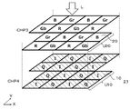
- the sensor includes a first semiconductor chip including a plurality of pixels, a first comparator connected to the first signal line, a first current circuit for passing a current through the first comparator, and a second comparator connected to the second signal line. Further, a second semiconductor chip including a second current circuit for passing a current through the second comparator may be provided, and the first semiconductor chip and the second semiconductor chip may be bonded to each other.
- the first and second semiconductor chips are electrically connected. May be done.
- the plurality of pixels may be an imaging pixel for acquiring an image of an object and a distance measuring pixel for measuring the distance to the object.
- the pixel transmits the signal voltage corresponding to the signal state in which the signal charge is accumulated in the first and second capacitor layers to the first and second signal lines, and then discharges the signal charge in the first and second capacitor layers.
- the reset voltage corresponding to the reset state of the above may be transmitted to the first and second signal lines, and the signal voltage and the reset voltage may be subjected to the correlation double sampling process.
- the pixels are provided on the first surface side in the semiconductor layer, and are provided on the first surface side of the second conductive type for accumulating charges from the first capacitor layer and on the first surface side in the semiconductor layer.
- a second conductive type second stray diffusion region for accumulating charges from the two capacitor layers is further provided, and a first signal line for transmitting a signal corresponding to the accumulated charges of the first capacitor layer and an accumulation of the second capacitor layer.
- a second signal line that transmits a signal according to the charge, a third signal line that transmits a signal corresponding to the accumulated charge in the first floating diffusion region, and a signal corresponding to the accumulated charge in the second floating diffusion region are transmitted.
- a fourth signal line may be further provided.
- the first floating diffusion region may accumulate the charge overflowing from the first capacitor layer
- the second floating diffusion region may accumulate the charge overflowing from the second capacitor layer
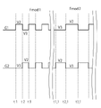
- the first and second capacitor layers accumulate charges from the photoelectric conversion unit distributed at the first frequency, and then transfer the charges to the first and second stray diffusion regions, respectively, and then the first and second capacitor layers are transferred to the first and second stray diffusion regions, respectively.
- Charges from the photoelectric conversion unit distributed at the second frequency may be accumulated.
- the sensor of the other aspect of the present disclosure is a sensor having a plurality of pixels, each of which is a photoelectric conversion unit that converts incident light into an electric charge, and a first and a first that alternately distributes an electric charge from the photoelectric conversion unit.
- the sensor stores the charges of the first and second memory units individually or collectively, the first stray diffusion region, and the second, which stores the charges of the third and fourth memory units individually or collectively.
- the first amplification transistor that outputs the voltage corresponding to the charge of the stray diffusion region and the first stray diffusion region to the first signal line
- the second signal line that outputs the voltage corresponding to the charge of the second stray diffusion region to the second signal line. 2 Amplification transistors may be further provided.
- the sensor has a common floating diffusion region that stores the charges of the first and second memory units individually or collectively, and stores the charges of the third and fourth memory units individually or collectively.
- a common amplification transistor that outputs a voltage corresponding to the charge in the floating diffusion region to the signal line may be further provided.
- the first and second memory units are connected in series between the first distribution transistor and the first amplification transistor, and the third and fourth memory units are connected in series between the second distribution transistor and the second amplification transistor. May be connected to.
- the first and second memory units may be connected in parallel, and the third and fourth memory units may be connected in parallel.
- the first and second memory units may transfer the electric charge to the CCD, and the third and fourth memory units may transfer the electric charge to the CCD.
- the sensor is provided on the first surface side in the semiconductor layer, and transmits a signal corresponding to the accumulated charge of the first capacitor layer and the first floating diffusion region of the second conductive type that stores the electric charge from the first capacitor layer.
- a third signal line for transmitting a signal corresponding to the accumulated charge in the first floating diffusion region may be further provided.
- the sensor may further include a source follower circuit provided between the first stray diffusion region and the third signal line.
- the pixel may further include a first transfer transistor that transfers the charge from the photoelectric conversion unit to the first capacitor layer.
- the pixel may further include a first selection transistor connected between the first amplification transistor and the first signal line.
- the pixel may further include a first reset transistor provided between the first capacitor layer and the first stray diffusion region, and a second reset transistor provided between the first stray diffusion region and the power supply. good.
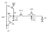
- the pixels are a first transfer transistor connected between the photoelectric conversion unit and the first floating diffusion region, and an overflow transistor and a second transfer transistor connected in series between the photoelectric conversion unit and the first floating diffusion region. And a third capacitive element connected between the node between the overflow transistor and the second transfer transistor and the reference power supply may be further provided.
- the pixels include a first transfer transistor connected between the photoelectric conversion unit and the first floating diffusion region, an overflow transistor provided between the photoelectric conversion unit and the first floating diffusion region, and a second transfer transistor.
- a CCD element provided between the overflow transistor and the second transfer transistor may be further provided.
- the sensors on the other side of the present disclosure are sensors having a plurality of pixels, each of which is a photoelectric conversion unit that converts incident light into electric charges and a first capacitor layer that stores electric charges from the photoelectric conversion unit.
- a first charge transistor provided above the first capacitor layer and accumulating charges from the photoelectric conversion unit to the first capacitor layer, a first stray diffusion region for accumulating charges from the first capacitor layer, and first. It includes a first transfer transistor provided between the stray diffusion region and the first charge capacitor.
- the sensor is provided between the first charge transistor and the first transfer transistor, is provided above the second capacitor layer and the second capacitor layer for accumulating the charge from the first capacitor layer, and is provided from the first capacitor layer. It may further include a second charge transistor that sends charges to the second capacitor layer.
- the sensor may further include a second transfer transistor provided between the photoelectric conversion unit and the first charge transistor.
- the plurality of pixels may be arranged so that the photoelectric conversion unit is unevenly distributed toward the center of the pixel region.
- the sensor on the other aspect of the present disclosure is a sensor that converts incident light into an electric charge and acquires an image corresponding to the electric charge, and is a plurality of shutter periods obtained by dividing an imaging period of one frame constituting the image.
- a photoelectric conversion unit that stores the electric charge generated in a part of the shutter period and a signal processing unit that estimates the signal of the entire frame from the electric charge in the part of the shutter period are provided.
- the signal processing unit may estimate that the signal of the entire frame is on a substantially linear extension line from the signal corresponding to the charge in a part of the shutter period.
- the sensor on the other aspect of the present disclosure is a sensor that converts incident light into an electric charge and acquires an image corresponding to the electric charge, and accumulates the electric charge generated during the imaging period of a plurality of frames constituting the image.
- the photoelectric conversion unit is provided, and a signal processing unit that estimates the signal of the first frame of the plurality of frames from the charges of the plurality of frames.
- the signal processing unit may estimate the average value of the signals corresponding to the charges in the periods of a plurality of frames as the signal of the first frame.
- FIG. 3 is a cross-sectional view showing a configuration example of a back-illuminated iTOF sensor according to a modified example of the first embodiment.
- FIG. 3 is a cross-sectional view showing a configuration example of a back-illuminated iTOF sensor according to another modification of the first embodiment.
- FIG. 3 is a cross-sectional view showing a configuration example of a back-illuminated iTOF sensor according to still another modification of the first embodiment.
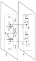
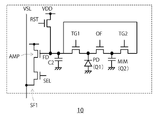
- the equivalent circuit diagram which shows an example of the composition of the pixel by 2nd Embodiment.
- the plan view which shows an example of the layout of the pixel by 2nd Embodiment.
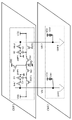
- the equivalent circuit diagram which shows an example of the composition of the pixel by 3rd Embodiment.
- the equivalent circuit diagram which shows an example of the composition of the pixel by 4th Embodiment.
- An equivalent circuit diagram showing an example of a pixel configuration according to a sixth embodiment The plan view which shows an example of the layout of the pixel by 6th Embodiment.
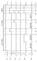
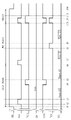
- the timing diagram which shows an example of the operation of a pixel by 6th Embodiment.
- the equivalent circuit diagram which shows an example of the composition of the pixel by 7th Embodiment.
- the plan view which shows an example of the layout of the pixel by 7th Embodiment.
- the equivalent circuit diagram which shows an example of the composition of the pixel by 8th Embodiment An equivalent circuit diagram showing an example of a pixel configuration according to a ninth embodiment.
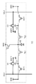
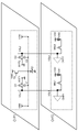
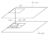
- An equivalent circuit diagram showing an example of a pixel configuration according to a tenth embodiment The plan view which shows an example of the layout of the pixel by 10th Embodiment. The timing diagram which shows an example of the operation of a pixel by 10th Embodiment. An equivalent circuit diagram showing an example of a pixel configuration according to the eleventh embodiment. An equivalent circuit diagram showing an example of a pixel configuration according to the twelfth embodiment. The equivalent circuit diagram which shows an example of the composition of the pixel by 13th Embodiment. The schematic diagram which shows the chip composition example of the pixel by 14th Embodiment. The schematic diagram which shows the chip composition example of the pixel by the fifteenth embodiment.
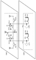
- the schematic diagram which shows the chip composition example of the pixel by 16th Embodiment The schematic diagram which shows the chip composition example of the pixel by 17th Embodiment.
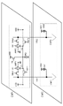
- the schematic diagram which shows the chip composition example of the pixel by 18th Embodiment The schematic diagram which shows the chip composition example of the pixel by 19th Embodiment.
- the schematic diagram which shows the chip composition example of the pixel by 20th Embodiment The schematic diagram which shows the chip composition example of the pixel by 21st Embodiment.
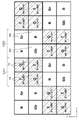
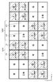
- the schematic diagram which shows the chip composition example of the pixel by 22nd Embodiment The plan view which shows an example of the pixel arrangement of the pixel area by 23rd Embodiment.
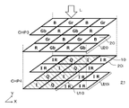
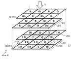
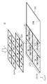
- FIG. 6 is a conceptual diagram showing an operation in a cross section along a line 55-55 in FIG.
- the plan view which shows an example of the layout of the pixel by 39th Embodiment.
- the timing diagram which shows an example of the operation of a pixel by 39th Embodiment.
- the timing diagram which shows the other example of the operation of a pixel by 39th Embodiment.
- the equivalent circuit diagram which shows the configuration example of the pixel by 40th Embodiment.
- FIG. 4 is a timing diagram showing another example of pixel operation according to the 40th embodiment.
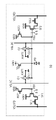
- the circuit diagram which shows an example of the composition of the pixel by 41st Embodiment.
- FIG. 5 is an equivalent circuit diagram showing an example of a pixel configuration according to the 53rd embodiment.
- FIG. 5 is an equivalent circuit diagram showing an example of a pixel configuration according to the 54th embodiment.
- FIG. 5 is an equivalent circuit diagram showing an example of a pixel configuration according to the 55th embodiment.
- the timing diagram which shows an example of the pixel reading operation by 55th Embodiment.
- the timing diagram which shows the other example of the pixel reading operation by 55th Embodiment.
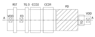
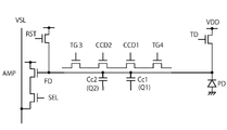
- FIG. 5 is an equivalent circuit diagram showing an example of a pixel configuration according to the 58th embodiment.
- the plan view which shows an example of the layout of the pixel by 58th Embodiment.
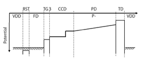
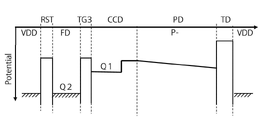
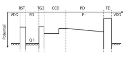
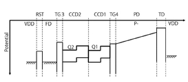
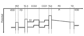
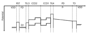
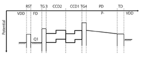
- FIG. 5 is a potential diagram showing the operation of pixels according to the 58th embodiment.
- FIG. 5 is a potential diagram showing the operation of pixels according to the 58th embodiment.
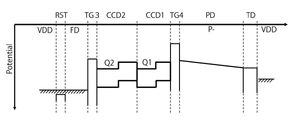
- FIG. 5 is a potential diagram showing the operation of pixels according to the 58th embodiment.
- FIG. 5 is a potential diagram showing the operation of pixels according to the 58th embodiment.
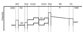
- FIG. 5 is a potential diagram showing the operation of pixels according to the 58th embodiment.
- FIG. 5 is a potential diagram showing the operation of pixels according to the 58th embodiment.
- FIG. 5 is a potential diagram showing the operation of pixels according to the 58th embodiment.
- FIG. 5 is a potential diagram showing the operation of pixels according to the 58th embodiment.
- FIG. 5 is a potential diagram showing the operation of pixels according to the 58th embodiment.
- FIG. 5 is a potential diagram showing the operation of pixels according to the 58th embodiment.
- FIG. 5 is a potential diagram showing the operation of pixels according to the 58th embodiment.
- FIG. 5 is a plan view showing an example of the layout of pixels according to the 59th embodiment.
- FIG. 5 is a potential diagram showing the operation of pixels according to the 59th embodiment.
- FIG. 5 is a potential diagram showing the operation of pixels according to the 59th embodiment.
- FIG. 5 is a potential diagram showing the operation of pixels according to the 59th embodiment.
- FIG. 5 is a potential diagram showing the operation of pixels according to the 59th embodiment.
- FIG. 5 is a potential diagram showing the operation of pixels according to the 59th embodiment.
- FIG. 5 is a potential diagram showing the operation of pixels according to the 59th embodiment.
- FIG. 5 is a potential diagram showing the operation of pixels according to the 59th embodiment.
- FIG. 5 is a potential diagram showing the operation of pixels according to the 59th embodiment.
- FIG. 5 is a potential diagram showing the operation of pixels according to the 59th embodiment.
- FIG. 5 is a potential diagram showing the operation of pixels according to the 59th embodiment.
- FIG. 5 is a potential diagram showing the operation of pixels according to the 59th embodiment.
- FIG. 5 is a potential diagram showing the operation of pixels according to the 59th embodiment.
- the equivalent circuit diagram which shows an example of the composition of the pixel by 60th Embodiment.
- the plan view which shows an example of the layout of the pixel by 60th Embodiment.
- the timing diagram which shows the operation of a pixel by 60th Embodiment.
- the potential figure which shows the operation of a pixel by 60th Embodiment The potential figure which shows the operation of a pixel by 60th Embodiment.
- the potential figure which shows the operation of a pixel by 60th Embodiment The potential figure which shows the operation of a pixel by 60th Embodiment.
- the potential figure which shows the operation of a pixel by 60th Embodiment The potential figure which shows the operation of a pixel by 60th Embodiment.
- the potential figure which shows the operation of a pixel by 60th Embodiment The potential figure which shows the operation of a pixel by 60th Embodiment.
- the potential figure which shows the operation of a pixel by 60th Embodiment The potential figure which shows the operation of a pixel by 60th Embodiment.
- the potential figure which shows the operation of a pixel by 60th Embodiment A layout diagram showing an example of pixels according to the 61st embodiment and a schematic diagram thereof.
- the schematic diagram which shows the arrangement example of the pixel in the pixel area by 61st Embodiment.
- the schematic diagram which shows the other arrangement example of the pixel in the pixel area by 61st Embodiment.
- the block diagram which shows the structural example of a light receiving element.
- the perspective view which shows the structural example of the light receiving element which can store the digital signal corresponding to the signal charge.
- the conceptual diagram which shows an example of the method of estimating the signal strength of each frame.
- the conceptual diagram which shows the other example of the method of estimating the signal strength of each frame.
- the conceptual diagram which shows an example of the operation method of the signal of each frame.
- the block diagram which shows the schematic configuration example of the vehicle control system which is an example of the mobile body control system to which the technique which concerns on this disclosure can be applied.
- the figure which shows the example of the installation position of the image pickup part.
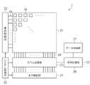
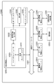
- FIG. 1 is a block diagram showing a configuration example of a distance measuring device according to the first embodiment.
- the distance measuring device 100 is a distance measuring sensor based on an indirect ToF (hereinafter, also referred to as iToF) method, and is used, for example, in an in-vehicle system mounted on a vehicle and measuring a distance to an object outside the vehicle. Further, the distance measuring device 100 may also be used for, for example, a system for identifying an individual such as face recognition.
- iToF indirect ToF
- the distance measuring device 100 includes a light receiving element 1, a light emitting element 2, a modulator 3, and a PLL (Phase Locked Loop) 4.
- PLL4 generates a pulse signal.
- the modulator 3 modulates the pulse signal from the PLL 4 to generate a control signal.
- the frequency of the control signal may be, for example, 5 megaHz to 200 megaHz.
- the light emitting element 2 emits light according to a control signal from the modulator.
- the light emitting element 2 has a light emitting diode that emits infrared light having a wavelength in the range of 780 nm to 1000 nm as a light source, and generates irradiation light in synchronization with a control signal of a square wave or a sine wave.
- the light generated by the light emitting element 2 may be, for example, short wave infrared light (SWIR (Short Wave Infrared Radiometer)) or the like.
- SWIR Short Wave Infrared Radiometer
- the irradiation light emitted from the light emitting element 2 is reflected by the object M and received by the light receiving element 1.
- the reflected light received by the light receiving element 1 is delayed from the timing when the light emitting element 2 emits light according to the distance to the object M.
- the delay time of the reflected light with respect to the irradiation light causes a phase difference between the irradiation light and the reflected light.
- the distance measuring device 100 calculates the phase difference between the irradiation light and the reflected light, and obtains the distance (depth information) from the distance measuring device 100 to the object M based on the phase difference.
- FIG. 2 is a block diagram showing a schematic configuration example of a light receiving element of the distance measuring device according to the first embodiment.
- the light receiving element 1 is an element used in the distance measuring device 100 according to the iToF method of FIG.
- the light receiving element 1 receives the light (reflected light) that is reflected and returned by the irradiation light generated by the light emitting element 2 as a light source, and outputs a depth image expressing the distance information to the object as a depth value. do.
- the light receiving element 1 has a pixel region 21 provided on a semiconductor substrate (not shown) and a peripheral circuit portion provided on the same semiconductor substrate.
- the peripheral circuit unit is composed of, for example, a vertical drive unit 22, a column processing unit 23, a horizontal drive unit 24, a system control unit 25, a signal processing unit 26, a data storage unit 27, and the like. All or part of the peripheral circuit portion may be provided on the same semiconductor substrate as the light receiving element 1, or may be provided on a substrate different from the light receiving element 1.
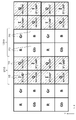
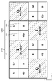
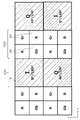
- the pixel region 21 has a plurality of pixels 10 two-dimensionally arranged in a matrix in the row direction and the column direction.
- the pixel 10 generates an electric charge according to the amount of received light, and outputs a signal corresponding to the electric charge. That is, the pixel 10 photoelectrically converts the incident light and outputs a signal corresponding to the electric charge obtained as a result.
- the details of the pixel 10 will be described later.
- the row direction is the horizontal direction in FIG. 2, and the column direction is the vertical direction.
- the pixel drive lines 28 are wired along the row direction for each pixel row with respect to the matrix-shaped pixel array, and two vertical signal lines 29 are arranged along the column direction in each pixel row. It is wired.
- the pixel drive line 28 transmits a drive signal for driving when reading a signal from the pixel 10.
- the pixel drive line 28 is shown as one wiring, but the wiring is not limited to one.
- One end of the pixel drive line 28 is connected to the output end corresponding to each line of the vertical drive unit 22.
- the vertical drive unit 22 is composed of a shift register, an address decoder, etc., and drives each pixel 10 of the pixel area 21 simultaneously for all pixels or in line units. That is, the vertical drive unit 22 constitutes a drive unit that controls the operation of each pixel 10 in the pixel region 21 together with the system control unit 25 that controls the vertical drive unit 22.
- the detection signal output from each pixel 10 of the pixel row according to the drive control by the vertical drive unit 22 is input to the column processing unit 23 through the vertical signal line 29.
- the column processing unit 23 performs predetermined signal processing on the detection signal output from each pixel 10 through the vertical signal line 29, and temporarily holds the detection signal after the signal processing. Specifically, the column processing unit 23 performs noise reduction processing, AD (Analog-to-Digital) conversion processing, and the like as signal processing.
- the horizontal drive unit 24 is composed of a shift register, an address decoder, etc., and sequentially selects unit circuits corresponding to the pixel strings of the column processing unit 23. By the selective scanning by the horizontal drive unit 24, the detection signals signal-processed for each unit circuit are sequentially output in the column processing unit 23.
- the system control unit 25 is composed of a timing generator or the like that generates various timing signals, and the vertical drive unit 22, the column processing unit 23, and the horizontal drive unit 24 are based on the various timing signals generated by the timing generator.
- Drive control such as.
- the signal processing unit 26 has an arithmetic processing function, and performs various signal processing such as arithmetic processing based on the detection signal output from the column processing unit 23.
- the data storage unit 27 temporarily stores data necessary for signal processing in the signal processing unit 26.
- the light receiving element 1 configured as described above includes the distance information to the object as a depth value in the pixel value, and outputs this pixel value as a depth image.
- the light receiving element 1 can be mounted on, for example, a vehicle-mounted system that is mounted on a vehicle and measures a distance to an object outside the vehicle.
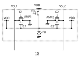
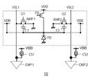
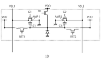
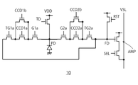
- FIG. 3 is an equivalent circuit diagram showing an example of the configuration of the pixel 10 according to the first embodiment.
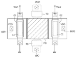
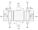
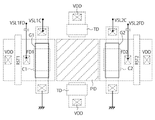
- FIG. 4 is a plan view showing an example of the layout of the pixels 10 according to the first embodiment.
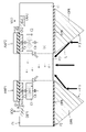
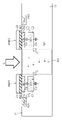
- FIG. 5 is a conceptual diagram showing the operation of the pixel 10.
- FIG. 5 shows a cross section along line AA of FIG.
- Each of the plurality of pixels 10 has the same configuration.
- the pixel 10 includes a photodiode PD, amplification transistors AMP1 and AMP2, capacitor layers C1 and C2, a power supply VDD, and vertical signal lines VSL1 and VSL2.
- the photodiode PD is a photoelectric conversion element that converts incident light into electric charges. As shown in FIG. 5, the photodiode PD is provided in the p-type semiconductor layer 11 as the first conductive type, and is provided between the amplification transistor AMP1 and the amplification transistor AMP2.
- the semiconductor layer 11 may be, for example, a silicon substrate, an epitaxial silicon layer, or the like.
- the source electrode of the amplification transistor AMP1 is connected to the vertical signal line VSL1, and the drain electrode thereof is grounded.
- the source electrode of the amplification transistor AMP2 is connected to the vertical signal line VSL2, and the drain electrode thereof is grounded.
- the amplification transistors AMP1 and AMP2 are both provided on the first surface F1 of the semiconductor layer 11, and are provided on both sides of the photodiode PD, respectively.
- the channel layers Ch1 and Ch2 of the amplification transistors AMP1 and AMP2 are p-type impurity diffusion layers provided on the first surface F1 side in the semiconductor layer 11, respectively.
- the gate electrodes G1 and G2 of the amplification transistors AMP1 and AMP2 are conductors provided above the channel layers Ch1 and Ch2, respectively, via the gate insulating films IN1 and IN2.
- the amplification transistors AMP1 and AMP2 receive the voltage of the gate electrodes G1 and G2 and enter a conductive state or a non-conducting state in the channel layers Ch1 and Ch2.
- the amplification transistors AMP1 and AMP2 are channel modulation transistors whose threshold voltage is modulated by the electric charge accumulated in the capacitor layers C1 and C2, respectively.
- the amplification transistors AMP1 and AMP2 are composed of, for example, a p-type MOSFET (Metal Oxide Semiconductor Field Effect Transistor).
- the amplification transistors AMP1 and AMP2 are channel modulation transistors, but do not have a ring structure. As a result, the area of the channel layers Ch1 and Ch2 can be reduced and the photoelectric conversion efficiency can be increased. As a result, kTC noise can be reduced. Further, when the capacitor layers C1 and C2 have a ring shape, the variation in the impurity charge distribution at the center of the ring causes variations in the performance of charge collection, storage and discharge between the taps of the capacitor layer C1 and the capacitor layer C2. Since the capacitor layers C1 and C2 according to the present embodiment have a substantially rectangular parallelepiped shape, it is possible to suppress variations in the performance of charge collection, storage, and discharge.
- the capacitor layers C1 and C2 are n - type impurity diffusion layers provided in the semiconductor layer 11 below the channel layers Ch1 and Ch2, respectively.
- the capacitor layers C1 and C2 can store the charge photoelectrically converted by the photodiode PD.
- the capacitor layer C1 is provided in the semiconductor layer 11 directly below the amplification transistor AMP1.
- the capacitor layer C1 is capacitively coupled to the channel layer Ch1 with a capacitive Ca, and is capacitively coupled to the semiconductor layer 11 with a capacitive Cb. Therefore, the threshold voltage of the amplification transistor AMP1 is modulated by the back bias effect depending on the amount of electric charge (for example, electron e ⁇ ) stored in the capacitor layer C1.
- the threshold voltage is modulated, even if the gate voltage is the same, the conduction state of the amplification transistor AMP1 changes, and the current or voltage of the vertical signal line VSL1 changes. Therefore, the vertical signal line VSL1 can transmit a voltage corresponding to the amount of electric charge stored in the capacitor layer C1.
- the capacitor layer C2 is provided in the semiconductor layer 11 directly below the amplification transistor AMP2.
- the capacitor layer C2 is capacitively coupled to the channel layer Ch2 with a capacitive Ca, and is capacitively coupled to the semiconductor layer 11 with a capacitive Cb. Therefore, the threshold voltage of the amplification transistor AMP2 is also modulated by the back bias effect depending on the amount of electric charge (for example, electron e ⁇ ) stored in the capacitor layer C2.
- the threshold voltage is modulated, even if the gate voltage is the same, the conduction state of the amplification transistor AMP2 changes, and the current or voltage of the vertical signal line VSL2 changes. Therefore, the vertical signal line VSL2 can transmit a voltage corresponding to the amount of electric charge stored in the capacitor layer C2.
- a gate electrode G1 is provided directly above the channel layer Ch1, and a capacitor layer C1 is provided directly below the channel layer Ch1. That is, the gate electrode G1 and the capacitor layer C1 are provided on opposite sides of the channel layer Ch1. As shown in FIG. 4, the gate electrode G1, the channel layer Ch1 and the capacitor layer C1 overlap each other in a plan view seen from the direction of light L incident on the semiconductor layer 11 (above the first surface F1 of the semiconductor layer 11). do.
- the channel layer Ch1 is a p-type impurity diffusion layer, and is of a reverse conductive type with respect to the capacitor layer C1.
- the sizes of the capacitor layers C1 and C2 are arbitrary in the plan view seen from the incident direction of L. For example, if the area of the capacitor layers C1 and C2 is increased, the photoelectric conversion efficiency is reduced, and if the area of the capacitor layers C1 and C2 is reduced, the photoelectric conversion efficiency is increased.
- the photoelectric conversion efficiency can be arbitrarily designed depending on the layout area of the capacitor layers C1 and C2.
- a gate electrode G2 is provided directly above the channel layer Ch2, and a capacitor layer C2 is provided directly below the channel layer Ch2. That is, the gate electrode G2 and the capacitor layer C2 are provided on opposite sides of the channel layer Ch2. As shown in FIG. 4, the gate electrode G2, the channel layer Ch2, and the capacitor layer C2 overlap each other in a plan view seen from above the first surface F1 of the semiconductor layer 11.
- the channel layer Ch2 is a p-type impurity diffusion layer, and is of a reverse conductive type with respect to the capacitor layer C2.
- the capacitor layers C1 and C2 are arranged on one side and the other side of the photodiode PD, respectively. Further, the amplification transistors AMP1 and AMP2 are also arranged on one side and the other side of the photodiode PD, respectively.
- the power supply diffusion layers DEF1 and DEF2 shown in FIGS. 4 and 5 are n + type impurity diffusion layers provided on the first surface F1 side in the semiconductor layer 11 and connected to the power supply VDD.
- the power supply diffusion layers DEF1 and DEF2 draw out the electric charges in the capacitor layers C1 and C2, and put the capacitor layers C1 and C2 in a reset state in which the electric charges are not accumulated.
- the vertical signal line VSL1 is connected to the source of the amplification transistor AMP1 and transmits a voltage corresponding to the threshold voltage of the amplification transistor AMP1 by passing a constant current.
- the vertical signal line VSL2 is connected to the source of the amplification transistor AMP2, and transmits a voltage corresponding to the threshold voltage of the amplification transistor AMP2 by passing a constant current.
- a current source is connected to the vertical signal lines VSL1 and VSL2. Since the amplification transistors AMP1 and AMP2 are p-type transistors, the current source is connected to the power supply side of the vertical signal lines VSL1 and VSL2. Further, as shown in FIG.
- a source follower circuit may be provided between the amplification transistors AMP1 and AMP2 and the vertical signal lines VSL1 and VSL2, respectively. Further, although not shown, the pixel 10 may have a current readout circuit configuration using a grounded-source circuit.
- the signal charge accumulated in the capacitor layers C1 and C2 is an electron, but the signal charge may be a hole.
- the light L is incident on the semiconductor layer 11 from the first surface F1. That is, the ranging device 100 of the present embodiment is a surface-illuminated iTOF sensor.
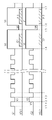
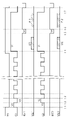
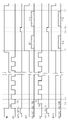
- FIG. 6 is a timing diagram showing an example of the operation of the pixel 10 according to the first embodiment.
- a reset operation for resetting the electric charge of the pixel 10 is performed on all the pixels.
- the stored charges of the photodiode PD and the capacitor layers C1 and C2 are discharged to the power supply VDD side.
- the amplification transistors AMP1 and AMP2 are driven alternately. For example, in the first period t1 to t2, the voltage of the gate electrode G1 rises to the high level V2 (collection voltage), and the voltage of the gate electrode G2 remains at the low level V3 (accumulated voltage). As a result, the amplification transistor AMP1 becomes a conductive state (hereinafter, on), and the amplification transistor AMP2 becomes a non-conducting state (hereinafter, off). At this time, the electric charge generated by the photodiode PD is transferred to the capacitor layer C1.
- the voltage of the gate electrode G2 rises to the high level V2, and the voltage of the gate electrode G1 falls to the low level V3.
- the amplification transistor AMP1 is turned off and the amplification transistor AMP2 is turned on.
- the electric charge generated in the photodiode PD is transferred to the capacitor layer C2.
- the electric charge generated by the photodiode PD is distributed and accumulated in the capacitor layers C1 and C2. In this case, the hole moves to the semiconductor layer 11 and is discharged.
- the first period t1 to t2 and the second period t2 to t3 are periodically and alternately repeated in synchronization with the irradiation light from the light emitting element 2.
- the capacitor layers C1 and C2 can accumulate charges according to the phase difference between the irradiation light from the light emitting element 2 of FIG. 1 and the reflected light received by the light receiving element 1.
- the relationship between the phase difference and the charges stored in the capacitor layers C1 and C2 will be described later.
- each pixel 10 in the pixel area 21 is sequentially selected.
- the read voltage V1 is applied to the gate electrodes G1 and G2 of the amplification transistors AMP1 and AMP2.
- the read voltage V1 is a voltage higher than the high level V2 at the time of charge accumulation.
- the amplification transistors AMP1 and AMP2 are brought into a conduction state according to the amount of electric charge accumulated in the capacitor layers C1 and C2, respectively.
- the vertical signal lines VSL1 and VSL2 transmit a voltage corresponding to the amount of electric charge stored in the capacitor layers C1 and C2, respectively.
- the vertical signal lines VSL1 and VSL2 receive the incident light L and transmit the signal voltages D1 and D2 corresponding to the signal charges generated by the photodiode PD, respectively.
- the reset voltage V4 is applied to the gate electrodes G1 and G2 of the amplification transistors AMP1 and AMP2.
- the reset voltage V4 is a voltage lower than the low level V3 at the time of charge accumulation.
- the amplification transistors AMP1 and AMP2 extract the signal charges accumulated in the capacitor layers C1 and C2, respectively, and discharge them to the power supply VDD.
- the signal charges are removed from the capacitor layers C1 and C2, and the capacitor layers C1 and C2 are in the reset state. That is, the pixel 10 is in a reset state in which the signal charge is not accumulated.
- each pixel 10 is sequentially selected.
- the read voltage V1 is also applied to the gate electrodes G1 and G2 of the amplification transistors AMP1 and AMP2.
- the amplification transistors AMP1 and AMP2 are brought into a conduction state according to the reset state of the capacitor layers C1 and C2, respectively.
- the vertical signal lines VSL1 and VSL2 transmit voltages according to the reset states of the capacitor layers C1 and C2, respectively.
- the vertical signal lines VSL1 and VSL2 transmit the reset voltages P1 and P2 corresponding to the capacitor layers C1 and C2 in the reset state in which the signal charges are not accumulated, respectively.
- the signal voltages D1 and D2 are output to the column processing unit 23 via the vertical signal lines VSL1 and VSL2, respectively, and then the reset voltages P1 and P2 are output to the column processing unit via the vertical signal lines VSL1 and VSL2, respectively. It is output to 23.
- the column processing unit 23 executes a correlated double sampling (CDS (Correlated Double Sampling)) process using the signal voltage D1 and the reset voltage P1. Thereby, an accurate signal component excluding the dark current component from the signal voltages D1 and D2 can be extracted.
- CDS Correlated Double Sampling
- the light L received by the pixel 10 is delayed from the timing of irradiation by the light source according to the distance to the object. Depending on the delay time according to the distance to the object, a phase difference occurs between the irradiation light and the reflected light, and the distribution ratio of the charges accumulated in the capacitor layer C1 and the capacitor layer C2 changes. Thereby, by detecting each potential of the capacitor layers C1 and C2, the phase difference between the irradiation light and the reflected light is calculated, and the distance to the object can be obtained based on this phase difference.
- the irradiation light is reflected by the object M in FIG. 1 and is received by the light receiving element 1.
- the frequency of the reflected light is the same as that of the illuminated light and remains Fmod.
- the time ⁇ t required from the emission of the irradiation light to the reflection on the object M and the return as the reflected light is the delay time (ToF) of the reflected light with respect to the irradiation light.
- the iToF uses the phase difference ⁇ between the irradiation light and the reflected light to measure the distance measuring device 100.
- the distance (depth information) D from the object M to the object M is calculated.
- the distance D is expressed by Equation 1.
- phase difference ⁇ is expressed by Equation 2.
- ⁇ arctan ((Q 90 -Q 270 ) / (Q 0 -Q 180 )) (Equation 2)
- the distance measuring device 100 can obtain the distance D (depth information) by using the iToF method.
- the amplification transistors AMP1 and AMP2 collect and store the electric charge generated by the photodiode PD in the capacitor layers C1 and C2, and the electric charge state (signal state or reset state) of the capacitor layers C1 and C2. ) Is being read. Further, the amplification transistors AMP1 and AMP2 also discharge (reset) the electric charge accumulated in the capacitor layers C1 and C2. As described above, since the amplification transistors AMP1 and AMP2 are channel modulation transistors having a plurality of functions, the pixel 10 according to the present embodiment can be composed of one photodiode PD and two transistors. As a result, each pixel 10 can be miniaturized, and the area of the pixel region 21 can be reduced.
- a channel modulation transistor is used for the amplification transistors AMP1 and AMP2.
- Capacitor layers C1 and C2 are provided below the channel layers Ch1 and Ch2, respectively, and the threshold voltage of the amplification transistors AMP1 and AMP2 is modulated depending on the amount of electric charge stored in the capacitor layers C1 and C2. Can be done.
- the reproducibility of the reset state is good.
- the electric charge in the floating diffusion region cannot be completely eliminated even if the floating diffusion region is reset. This is because the floating diffusion region is connected to the metal wiring, so that some electric charges enter the floating diffusion region from the metal wiring.
- the amount of electric charge in the floating diffusion region changes and the signal in the reset state varies. That is, the reproducibility of the reset state is not good. Therefore, if the reset state is detected after the signal state is detected, the reset state does not correspond to the noise component of the signal state, and an accurate signal component cannot be extracted even if the CDS processing is performed.
- the reproducibility of the reset state is good, so that the signal processing unit 26 is accurate with less kTC noise even if the reset state detected after the signal state is excluded from the signal state. Signal components can be extracted.
- the size of the pixel 10 can be reduced, and a signal component with less kTC noise can be obtained by CDS processing.
- the amplification transistors AMP1 and AMP2 are provided with capacitor layers C1 and C2 on the substrate side under the channel layers Ch1 and Ch2.
- the capacitor layers C1 and C2 are pocket regions for accumulating signal charges.
- the capacitor layers C1 and C2 can be formed in a small volume and capacity.
- the channel layers Ch1 and Ch2 and the semiconductor layer 11 are in contact with the capacitor layers C1 and C2 via the capacities Ca and Cb of a very small depletion layer having a PN junction. Therefore, in the amplification transistors AMP1 and AMP2, the output voltage value (photoelectric conversion efficiency) per electric charge becomes very high. Thereby, the sensitivity of the pixel 10 can be improved. Further, kTC noise can be reduced even when the light L has low illuminance.
- the capacitor layers C1 and C2 can be formed on a p-type substrate which is cheaper than an n-type substrate. Therefore, this embodiment can suppress an increase in manufacturing cost.
- FIG. 7 is a cross-sectional view showing a configuration example of a back-illuminated iTOF sensor according to a modified example of the first embodiment.
- the back-illuminated iTOF sensor In the back-illuminated iTOF sensor, light L is incident from the second surface F2 of the semiconductor layer 11 on the side opposite to the first surface F1.
- the present embodiment can also be applied to a back-illuminated iTOF sensor.
- FIG. 8 is a cross-sectional view showing a configuration example of a back-illuminated iTOF sensor according to another modification of the first embodiment.
- the light-shielding film OPB is provided in a region of the second surface F2 of the semiconductor layer 11 other than the photodiode PD.
- the light-shielding film OPB is provided so as to overlap the capacitor layers C1 and C2, and is provided so as not to overlap the photodiode PD.
- an opaque metal material that does not transmit light is used for the light-shielding film OPB.
- the light-shielding film OPB does not transmit light L in a region other than the photodiode PD. As a result, it is possible to suppress the light L from entering the capacitor layers C1 and C2, and it is possible to reduce the PLS (Parasitic Light Sensitivity).
- FIG. 9 is a cross-sectional view showing a configuration example of a back-illuminated iTOF sensor according to still another modification of the first embodiment.
- the reflective film OPR is provided on the light-shielding film OPB. Similar to the light-shielding film OPB, the reflective film OPR is provided in a region of the second surface F2 of the semiconductor layer 11 other than the photodiode PD. In a plan view seen from the incident direction of the light L, the reflective film OPR is provided so as to overlap the capacitor layers C1 and C2, and reflects the light on the photodiode PD.
- the reflective film OP is in contact with other materials (not shown) such as the atmosphere, silicon, and a silicon oxide film on the reflective surface F3, and reflects light L at the interface thereof.
- the reflective surface F3 is a side surface of the reflective film OVER inclined with respect to the incident direction of the light L.
- the reflective film OP is a low refractive index material (eg, polymer (refractive index 1.29), low refractive index) having a lower refractive index than the material in contact with the reflective surface F3 (eg, atmosphere, silicon, silicon oxide film, etc.). Resins (refractive index 1.33), fluororesin coating materials (refractive index 1.34), UV curable low refractive index resins (refractive index 1.40), etc.) are used.
- the reflective film OP can totally reflect the light L on the reflecting surface F3.
- OCL on-chip lens
- FIG. 10 is an equivalent circuit diagram showing an example of the configuration of the pixel 10 according to the second embodiment.
- FIG. 11 is a plan view showing an example of the layout of the pixels 10 according to the second embodiment.
- each of the pixels 10 further includes a charge discharge transistor TD that discharges the charge of the photodiode PD.
- the charge discharge transistor TD is connected between the power supply VDD and the cathode of the photodiode PD, and can discharge the charge (for example, electrons) stored in the photodiode PD to the power supply VDD.
- the charge discharge transistor TD is arranged so as to be adjacent to the upper and lower two sides of the photodiode PD.
- the charge discharge transistor TD is, for example, an n-type MOSFET. When the photodiode PD receives the light L, the charge discharge transistor TD is turned off.
- the charge discharge transistor TD When the photodiode PD is not receiving light L, the charge discharge transistor TD is turned on. For example, the charge discharge transistor TD is turned off during the light receiving period from t1 to t4 in FIG. 6, and the charge discharge transistor TD is turned on during the detection period from t4 to t7. As a result, it is possible to prevent unnecessary charges (noise) from being mixed into the capacitor layers C1 and C2 due to background light such as sunlight. As a result, the distance measuring accuracy of the distance measuring device 100 can be improved. Further, since the capacitor layers C1 and C2 are not ring-shaped but substantially rectangular parallelepiped, the charge discharge transistor TD tends to discharge charges from the capacitor layers C1 and C2 at the time of reset.
- FIG. 12 is an equivalent circuit diagram showing an example of the configuration of the pixel 10 according to the third embodiment.
- the pixel 10 further includes a comparator CMP1 as a first comparator, a comparator CMP2 as a second comparator, a current circuit CS1 as a first current circuit, and a current circuit CS2 as a second current circuit.
- the comparators CMP1 and CMP2 are connected to the vertical signal lines VSL1 and VSL2, respectively, and are provided in each pixel 10. Further, the current circuits CS1 and CS2 are connected between the power supply VDD and the vertical signal lines VSL1 and VSL2, respectively, and a current is passed through the vertical signal lines VSL1 and VSL2, respectively.
- third embodiment may be the same as the corresponding configurations of the first or second embodiment. Thereby, the third embodiment can also obtain the effect of the first or second embodiment.
- FIG. 13 is an equivalent circuit diagram showing an example of the configuration of the pixel 10 according to the fourth embodiment.
- the connection relationship between the cathode and the anode of the photodiode PD is opposite to that of the third embodiment.
- the capacitor layers C1 and C2 are composed of a p-type impurity diffusion layer and accumulate holes.
- the amplification transistors AMP1 and AMP2 are composed of an n-type well or an n-type MOSFET formed on an n-type substrate.
- the current circuits CS1 and CS2 are connected between the power supply VDD and the vertical signal lines VSL1 and VSL2, respectively, and a current flows in the direction opposite to the current circuits CS1 and CS2 of the third embodiment.
- the pixel 10 can accumulate the hole as a signal charge and detect the signal component.
- the pixel 10 of the fourth embodiment can be manufactured at low cost. Further, since the amplification transistors AMP1 and AMP2 are n-type MOSFETs, reading is possible with the same circuit configuration as the source follower circuit of the CMOS image sensor. Further, the capacitor layers C1 and C2 that accumulate holes have a voltage close to zero in the reset state, and the dark current is small. Therefore, the pixel 10 of the fourth embodiment can reduce the random noise.
- FIG. 14 is an equivalent circuit diagram showing an example of the configuration of the pixel 10 according to the fifth embodiment.
- the pixel 10 is a transfer transistor TRS1, TRS2, a capacitor element C3, a capacitor element C4, a reset transistor RST1, RST2, a source follower circuit SF1, a source follower circuit SF2, and a selection transistor SEL1. It is equipped with SEL2. Further, the vertical signal lines VSL1 and VSL2 are provided with current circuits CS1 and CS2, respectively.
- the transfer transistors TRS1 and TRS2 are provided between the sources of the amplification transistors AMP1 and AMP2 and the capacitor elements C3 and C4, respectively.
- the transfer transistor TRS1 is composed of, for example, an n-type MOSFET.
- the capacitor element C3 as the first capacitance element is connected between the transfer transistor TRS1 and the ground, and can store the electric charge from the amplification transistor AMP1 via the transfer transistor TRS1.
- the capacitor element C4 as the second capacitance element is connected between the transfer transistor TRS2 and the ground, and can store the electric charge from the amplification transistor AMP2 via the transfer transistor TRS2.
- the capacitor elements C3 and C4 may be composed of a capacitive element such as a MoM (Metal-on-Metal), a MIM (Metal-Insulator-Metal), or a MOS capacitor. Therefore, the capacitor elements C3 and C4 can have a sufficiently larger capacity than the capacitor layers C1 and C2 composed of the impurity diffusion layer, and can suppress the generation of noise.
- the reset transistor RST1 is connected between the capacitor element C3 and the power supply VDD, and the charge of the capacitor element C3 can be discharged to perform the reset operation.
- the reset transistor RST2 is connected between the capacitor element C4 and the power supply VDD, and can discharge the electric charge of the capacitor element C4 to perform the reset operation.
- the source follower circuit SF1 as the first source follower circuit is connected to the capacitor element C3 via the transfer transistor TRS1 and connected to the vertical signal line VSL1 via the selection transistor SEL1.
- the source follower circuit SF1 transmits a voltage corresponding to the amount of electric charge of the capacitor element C3 to the vertical signal line VSL1.
- the source follower circuit SF2 as the second source follower circuit is connected to the capacitor element C4 via the transfer transistor TRS2 and connected to the vertical signal line VSL2 via the selection transistor SEL2.
- the source follower circuit SF2 transmits a voltage corresponding to the amount of electric charge of the capacitor element C4 to the vertical signal line VSL2.
- the capacitor elements C3 and C4 and the source follower circuits SF1 and SF2 generate a signal voltage converted from the signal charge in the pixel 10, and transmit the signal voltage to the vertical signal lines VSL1 and VSL2, respectively. do. That is, the pixel 10 according to the fifth embodiment is a pixel of the voltage domain. As a result, the capacitor elements C3 and C4 are not provided in the semiconductor layer 11, and it is not necessary to store electric charges in the semiconductor layer 11. Therefore, the area of the semiconductor layer 11 can be reduced. As a result, the dark current generated in the semiconductor layer 11 can be reduced.
- FIG. 15 is an equivalent circuit diagram showing an example of the configuration of the pixel 10 according to the sixth embodiment.
- FIG. 16 is a plan view showing an example of the layout of the pixels 10 according to the sixth embodiment.
- the pixel 10 further includes transfer transistors TG1 and TG2.
- the transfer transistor TG1 is provided between the photodiode PD and the capacitor layer C1, and transfers the electric charge from the photodiode PD to the capacitor layer C1.
- the transfer transistor TG2 is provided between the photodiode PD and the capacitor layer C2, and transfers the electric charge from the photodiode PD to the capacitor layer C2.
- FIG. 16 in a plan view seen from the incident direction of the light L, two transfer transistors TG1 and TG2 are provided on each opposite side of the pair of photodiode PDs. As a result, the potential in the photodiode PD can be inclined, and the electric charge can be collected quickly.
- the signal charge path does not have an interface between the semiconductor layer 11 and the silicon oxide film.
- the signal charge does not pass through such an interface and is not trapped or detrapped along the way. Therefore, the transfer transistors TG1 and TG2 can smoothly transfer the signal charge.
- the transfer transistors TG1 and TG2 have a charge collecting function among the functions of the amplification transistors AMP1 and AMP2 of the second embodiment.
- FIG. 17 is a timing diagram showing an example of the operation of the pixel 10 according to the sixth embodiment.
- the transfer transistors TG1 and TG2 are responsible for the charge collection function. Therefore, during the light receiving period t1 to t4, the gate voltages of the transfer transistors TG1 and TG2 are alternately on / off controlled by the collection voltage V2 and the low level voltage. As a result, the electric charge generated by the photodiode PD is distributed to the capacitor layers C1 and C2. At this time, the gate voltage of the amplification transistors AMP1 and AMP2 is maintained at the low level storage voltage V3, and the amplification transistors AMP1 and AMP2 store charges in the capacitor layers C1 and C2.
- the charge discharge transistor TD When the light receiving period t1 to t4 ends, the charge discharge transistor TD is turned on, and the charge is discharged from the photodiode PD to reset.
- the read operation described with reference to FIG. 6 is executed.
- the signal voltages D1 and D2 are output to the column processing unit 23 via the vertical signal lines VSL1 and VSL2, respectively, and then the reset voltages P1 and P2 are output to the column processing unit via the vertical signal lines VSL1 and VSL2, respectively. It is output to 23.
- the column processing unit 23 executes CDS processing using the signal voltages D1 and D2 and the reset voltages P1 and P2.
- the number of transistors constituting each pixel 10 is increased by the amount of the transfer transistors TG1 and TG2.
- the transfer transistors TG1 and TG2 execute the charge collection function
- the gate voltage of the amplification transistors AMP1 and AMP2 does not need to be the collection voltage V2. Therefore, the operating margin of the amplification transistors AMP1 and AMP2 can be expanded, and the dynamic range of the signal voltage of the vertical signal lines VSL1 and VSL2 can be expanded. Further, since the drive voltage of the transfer transistors TG1 and TG2 can be lowered, the power consumption can be reduced.
- sixth embodiment may be the same as the corresponding configurations of the second embodiment. Therefore, the sixth embodiment can also obtain the effect of the second embodiment.
- the sixth embodiment may be combined with other embodiments other than the second embodiment.
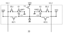
- FIG. 18 is an equivalent circuit diagram showing an example of the configuration of the pixel 10 according to the seventh embodiment.
- FIG. 19 is a plan view showing an example of the layout of the pixel 10 according to the seventh embodiment.
- the pixel 10 further includes the selection transistors SEL1 and SEL2.
- the selection transistor SEL1 as the first selection transistor is provided between the amplification transistor AMP1 and the vertical signal line VSL1, and when the pixel 10 is selected, the amplification transistor AMP1 and the vertical signal line VSL1 are provided. Connect between.
- the selection transistor SEL1 can transmit a voltage corresponding to the conduction state of the amplification transistor AMP1 to the vertical signal line VSL1.
- the selection transistor SEL2 as the second selection transistor is provided between the amplification transistor AMP2 and the vertical signal line VSL2, and connects between the amplification transistor AMP2 and the vertical signal line VSL2 when the pixel 10 is selected. ..
- the selection transistor SEL2 can transmit a voltage corresponding to the conduction state of the amplification transistor AMP2 to the vertical signal line VSL2.
- the selection transistors SEL1 and SEL2 are provided between the amplification transistors AMP1 and AMP2 and the vertical signal lines VSL1 and VSL2, respectively.
- the selection transistors SEL1 and SEL2 are composed of, for example, a p-type MOSFET.
- FIG. 20 is a timing diagram showing an example of the operation of the pixel 10 according to the seventh embodiment. Since the selection transistors SEL1 and SEL2 are p-type MOSFETs, low-active switching is performed.
- the selection transistors SEL1 and SEL2 are responsible for reading out the signal state and the reset state. Therefore, during the light receiving periods t1 to t4, the selection transistors SEL1 and SEL2 are turned off, and the collection and storage operations described with reference to FIG. 6 are executed. After that, in the read period t4 to t7, the selection transistors SEL1 and SEL2 of the selected pixel 10 are turned on, whereby the signal voltages D1 and D2 are read out to the vertical signal lines VSL1 and VSL2, respectively. Next, after the reset operation, the reset voltages P1 and P2 are read out to the vertical signal lines VSL1 and VSL2, respectively.
- the column processing unit 23 executes CDS processing using the signal voltages D1 and D2 and the reset voltages P1 and P2.
- the number of transistors constituting each pixel 10 is increased by the amount of the selection transistors SEL1 and SEL2.
- the selection transistors SEL1 and SEL2 by independently providing the selection transistors SEL1 and SEL2, row selection in the pixel region 21 can be facilitated, and crosstalk between rows can be suppressed.
- the distance measuring device 100 can obtain highly accurate distance measuring performance.
- the selection transistors SEL1 and SEL2 to execute the read function, the gate voltage of the amplification transistors AMP1 and AMP2 does not need to be set to the read voltage V1. Therefore, the operating margin of the amplification transistors AMP1 and AMP2 can be expanded, and the dynamic range of the signal voltage of the vertical signal lines VSL1 and VSL2 can be expanded.
- the seventh embodiment may be the same as the corresponding configurations of the second embodiment. Therefore, the seventh embodiment can also obtain the effect of the second embodiment.
- the seventh embodiment may be combined with other embodiments other than the second embodiment.
- FIG. 21 is an equivalent circuit diagram showing an example of the configuration of the pixel 10 according to the eighth embodiment.
- the vertical signal lines VSL1 and VSL2 are connected to the comparators CMP1 and CMP2 and the current circuits CS1 and CS2 of the third embodiment, respectively.
- a comparator and a constant current source may be arranged for each pixel. In this case, since the movement is for each pixel, the reading can be randomly accessed, and it is not necessary to read in order.
- the eighth embodiment may be applied to the distance measuring device 100 that simultaneously accumulates electric charges in all the pixels 10.
- the eighth embodiment may be the same as the corresponding configurations of the seventh embodiment. Therefore, the eighth embodiment can also obtain the effect of the seventh embodiment.
- the eighth embodiment may be combined with other embodiments other than the seventh embodiment.
- FIG. 22 is an equivalent circuit diagram showing an example of the configuration of the pixel 10 according to the ninth embodiment.
- the vertical signal lines VSL1 and VSL2 share the comparator CMP2 and the current circuit CS2, and are connected to the common comparator CMP2 and the current circuit CS2.
- the gain variation and the offset variation of the comparator are standardized.
- the ninth embodiment may be the same as the corresponding configurations of the seventh embodiment. Therefore, the ninth embodiment can also obtain the effect of the seventh embodiment.
- the ninth embodiment may be combined with other embodiments other than the seventh embodiment.
- FIG. 23 is an equivalent circuit diagram showing an example of the configuration of the pixel 10 according to the tenth embodiment.
- FIG. 24 is a plan view showing an example of the layout of the pixel 10 according to the tenth embodiment.
- the pixel 10 further includes reset transistors RST1 and RST2.
- the reset transistor RST1 as the first reset transistor is provided between the capacitor layer C1 and the power supply VDD, and connects between the capacitor layer C1 and the power supply VDD when the capacitor layer C1 is reset. ..
- the reset transistor RST1 discharges electric charge from the capacitor layer C1 to reset the capacitor layer C1.
- the reset transistor RST2 as the second reset transistor is provided between the capacitor layer C2 and the power supply VDD, and is connected between the capacitor layer C2 and the power supply VDD when the capacitor layer C2 is reset.
- the reset transistor RST2 discharges electric charge from the capacitor layer C2 to reset the capacitor layer C2.
- the reset transistors RST1 and RST2 are arranged between the capacitor layers C1 and C2 and the power supply VDD, respectively, in a plan view seen from the incident direction of the light L. Since the amplification transistors AMP1 and AMP2 are directly above the capacitor layers C1 and C2, it can be said that the reset transistors RST1 and RST2 are arranged between the amplification transistors AMP1 and AMP2 and the power supply VDD, respectively.
- the reset transistors RST1 and RST2 are composed of, for example, a p-type MOSFET.
- FIG. 25 is a timing diagram showing an example of the operation of the pixel 10 according to the tenth embodiment. Since the reset transistors RST1 and RST2 are p-type MOSFETs, low-active switching is performed.
- the reset transistors RST1 and RST2 are responsible for the reset operation. Therefore, during the light receiving periods t1 to t4, the reset transistors RST1 and RST2 are off, and the collection and storage operations described with reference to FIG. 6 are executed. After that, in the read period t4 to t5, the amplification transistors AMP1 and AMP2 of the selected pixel 10 are turned on, whereby the signal voltages D1 and D2 are read out to the vertical signal lines VSL1 and VSL2, respectively.
- the reset transistors RST1 and RST2 execute the reset operation.
- the reset transistors RST1 and RST2 discharge the charges of the capacitor layers C1 and C2 to the power supply VDD.
- the gate voltage of the amplification transistors AMP1 and AMP2 maintains the high level V1, and the amplification transistors AMP1 and AMP2 maintain the ON state.
- the reset transistors RST1 and RST2 are turned off during the read-out period t6 to t7 in the reset state, the reset voltages P1 and P2 are read out to the vertical signal lines VSL1 and VSL2, respectively.
- the column processing unit 23 executes CDS processing using the signal voltages D1 and D2 and the reset voltages P1 and P2.
- the number of transistors constituting each pixel 10 is increased by the amount of the reset transistors RST1 and RST2.
- the gate voltage of the amplification transistors AMP1 and AMP2 does not need to be the reset voltage V4. Therefore, the operating margin of the amplification transistors AMP1 and AMP2 can be expanded, and the dynamic range of the signal voltage of the vertical signal lines VSL1 and VSL2 can be expanded. Further, the operating margin of the reset transistors RST1 and RST2 can be expanded.
- the tenth embodiment may be the same as the corresponding configurations of the second embodiment. Therefore, the tenth embodiment can also obtain the effect of the second embodiment.
- the tenth embodiment may be combined with other embodiments other than the second embodiment.
- FIG. 26 is an equivalent circuit diagram showing an example of the configuration of the pixel 10 according to the eleventh embodiment.
- the pixel 10 further includes selection transistors SEL1 and SEL2 and reset transistors RST1 and RST2. That is, the eleventh embodiment is a combination of the seventh and tenth embodiments. Therefore, the eleventh embodiment can obtain the effects of the seventh and tenth embodiments.
- the amplification transistors AMP1 and AMP2, the selection transistors SEL1 and SEL2, and the reset transistors RST1 and RST2 are all composed of p-type MOSFETs.
- the signal charge is an electron
- the capacitor layers C1 and C2 for accumulating the electron are composed of an n-type impurity diffusion layer. Therefore, each channel of the amplification transistors AMP1 and AMP2, the selection transistors SEL1 and SEL2, and the reset transistors RST1 and RST2 needs to be a reverse conductive type p type with the capacitor layers C1 and C2. Therefore, the amplification transistors AMP1 and AMP2, the selection transistors SEL1 and SEL2, and the reset transistors RST1 and RST2 are all composed of p-type MOSFETs.
- the plane configuration and operation of the eleventh embodiment can be easily understood from the seventh and tenth embodiments. Therefore, the plan view and the timing diagram of the eleventh embodiment are omitted here.
- FIG. 27 is an equivalent circuit diagram showing an example of the configuration of the pixel 10 according to the twelfth embodiment.
- the pixel 10 further includes transfer transistors TG1 and TG2 and reset transistors RST1 and RST2. That is, the twelfth embodiment is a combination of the sixth and tenth embodiments. Therefore, the twelfth embodiment can obtain the effects of the sixth and tenth embodiments.
- FIG. 28 is an equivalent circuit diagram showing an example of the configuration of the pixel 10 according to the thirteenth embodiment.
- the pixel 10 further includes transfer transistors TG1 and TG2, reset transistors RST1 and RST2, and selection transistors SEL1 and SEL2. That is, the thirteenth embodiment is a combination of the sixth, seventh and tenth embodiments. Therefore, the thirteenth embodiment can obtain the effects of the sixth, seventh and tenth embodiments.
- the plane configuration and operation of the thirteenth embodiment can be easily understood from the sixth, seventh and tenth embodiments. Therefore, the plan view and the timing diagram of the thirteenth embodiment are omitted here.
- FIG. 29 is a schematic view showing a chip configuration example of the pixel 10 according to the 14th embodiment.
- the pixel 10 is formed on the semiconductor chip CHP1, and the circuits other than the pixel 10 are formed on the semiconductor chip CHP2. That is, the distance measuring device 100 is divided into semiconductor chips CHP1 and CHP2.
- the semiconductor chips CHP1 and CHP2 are bonded to each other for wiring and connection.
- the pixel 10 according to the third embodiment is shown.
- the semiconductor chip CHP1 mounts a pixel 10 including a photodiode PD, amplification transistors AMP1 and AMP2, capacitor layers C1 and C2, and a charge discharge transistor TD.
- the semiconductor chip CHP2 mounts the comparators CMP1 and CMP2 and the current circuits CS1 and CS2.
- the vertical signal lines VSL1 and VSL2 are wired and joined at the bonding surface between the semiconductor chip 1 and the semiconductor chip 2, respectively.
- the amplification transistor AMP1 of the semiconductor chip CHP1 is connected to the comparator CMP1 of the semiconductor chip CHP2 and the current circuit CS1 via a wire-bonded vertical signal line VSL1.
- the amplification transistor AMP2 of the semiconductor chip CHP2 is connected to the comparator CMP2 of the semiconductor chip CHP2 and the current circuit CS2 via a wire-bonded vertical signal line VSL2.
- the semiconductor chips CHP1 and CHP2 are electrically connected by joining the vertical signal lines VSL1 and VSL2 of the semiconductor chips CHP1 and CHP2, respectively.
- the vertical signal lines VSL1 and VSL2 are provided for each pixel column, and are provided in the same number as the number of pixels 10 in one pixel row. Therefore, in the semiconductor chip CHP2, the comparators CMP1 and CMP2 and the current circuits CS1 and CS2 are also provided for each pixel column, and are provided in the same number as the number of pixels 10 included in one pixel row. As a result, the comparators CMP1 and CMP2 and the current circuits CS1 and CS2 are shared by each pixel sequence, so that the layout area of the comparators CMP1 and CMP2 and the current circuits CS1 and CS2 becomes small. Further, the comparators CMP1 and CMP2 and the current circuits CS1 and CS2 can simultaneously detect signals from a plurality of pixels 10 included in one pixel row.
- the vertical signal lines VSL1 and VSL2 may be provided in the same number as the number of pixels 10 included in the plurality of pixel rows.
- the comparators CMP1 and CMP2 and the current circuits CS1 and CS2 are arranged in the same number as the number of pixels 10 in the plurality of pixel rows corresponding to the vertical signal lines VSL1 and VSL2.
- the vertical signal lines VSL1 and VSL2 may be provided corresponding to each pixel 10 of the semiconductor chip CHP1.
- the comparators CMP1 and CMP2 and the current circuits CS1 and CS2 are arranged in the same number as the number of pixels 10 of the semiconductor chip CHP1 corresponding to the vertical signal lines VSL1 and VSL2.
- the vertical signal lines VSL1, VSL2, comparators CMP1, CMP2 and the current circuits CS1 and CS2 are provided for each pixel 10 of the semiconductor chip CHP1, it is possible to execute the global shutter operation on the pixel 10 without dropping the saturation signal. can.
- the distance measuring device 100 can be used as a dynamic vision sensor that outputs a signal when the signal change of each pixel 10 is equal to or more than a certain threshold value.
- the 14th embodiment can be applied to embodiments other than the 2nd embodiment.
- the configuration of the broken line portion shown in FIGS. 13 to 15, 18, 18, 21 to 23, and 26 to 28 is mounted on the semiconductor chip CHP1, and other configurations such as a comparator and a current circuit are mounted on the semiconductor chip CHP2. It should be installed.
- the selection transistors SEL1 and SEL2 are independent of the amplification transistors AMP1 and AMP2, the pixel 10 can selectively turn on one of the selection transistors SEL1 and SEL2 to read the signal. .. In this case, crosstalk between adjacent vertical signal lines VSL1 and VSL2 can be suppressed.
- FIG. 30 is a schematic view showing a chip configuration example of the pixel 10 according to the fifteenth embodiment.
- the semiconductor chip CHP1 mounts a photodiode PD, amplification transistors AMP1, AMP2, transfer transistors TG1, TG2, capacitor layers C1, C2, and charge emission transistors TD.
- the semiconductor chip CHP2 mounts the comparators CMP1 and CMP2 and the current circuits CS1 and CS2.
- the configuration of the transfer transistors TG1 and TG2 may be the same as that of the sixth embodiment. Further, the other configurations of the fifteenth embodiment may be the same as the configurations of the fourteenth embodiment. Therefore, in the fifteenth embodiment, the vertical signal lines VSL1, VSL2, the comparators CMP1, CMP2, and the current circuits CS1 and CS2 are provided corresponding to each pixel row, and are provided in the same number as the number of pixels 10 in one pixel row. You may. Further, the vertical signal lines VSL1 and VSL2, the comparators CMP1 and CMP2, and the current circuits CS1 and CS2 may be provided corresponding to the pixels 10 included in the plurality of pixel rows.
- the vertical signal lines VSL1, VSL2, comparators CMP1, CMP2, and current circuits CS1 and CS2 are provided corresponding to each pixel 10 of the semiconductor chip CHP1, and even if the same number as the number of pixels 10 in the semiconductor chip CHP1 is provided. good.
- FIG. 31 is a schematic view showing a chip configuration example of the pixel 10 according to the 16th embodiment.
- the semiconductor chip CHP1 includes a photodiode PD, amplification transistors AMP1, AMP2, selection transistors SEL1, SEL2, capacitor layers C1 and C2, and a charge discharge transistor TD.
- the semiconductor chip CHP2 mounts the comparators CMP1 and CMP2 and the current circuits CS1 and CS2.
- the configuration of the selection transistors SEL1 and SEL2 may be the same as that of the seventh embodiment. Further, the other configurations of the 16th embodiment may be the same as the configurations of the 14th embodiment. Therefore, in the 16th embodiment, the vertical signal lines VSL1, VSL2, the comparators CMP1, CMP2, and the current circuits CS1 and CS2 are provided corresponding to each pixel row, and are provided in the same number as the number of pixels 10 in one pixel row. You may. Further, the vertical signal lines VSL1 and VSL2, the comparators CMP1 and CMP2, and the current circuits CS1 and CS2 may be provided corresponding to the pixels 10 included in the plurality of pixel rows.
- the vertical signal lines VSL1, VSL2, comparators CMP1, CMP2, and current circuits CS1 and CS2 are provided corresponding to each pixel 10 of the semiconductor chip CHP1, and may be provided in the same number as the number of pixels 10 in the semiconductor chip CHP1. ..
- FIG. 32 is a schematic view showing a chip configuration example of the pixel 10 according to the 17th embodiment.
- the pixel 10 according to the eighth embodiment is shown.
- the selection transistors SEL1 and SEL2 are provided on the semiconductor chip CHP2. That is, the semiconductor chip CHP1 mounts a photodiode PD, amplification transistors AMP1, AMP2, capacitor layers C1 and C2, and a charge discharge transistor TD.
- the semiconductor chip CHP2 mounts the comparators CMP1 and CMP2, the selection transistors SEL1 and SEL2, and the current circuits CS1 and CS2.
- the semiconductor chip CHP2 mounts the selection transistors SEL1 and SEL2 in addition to the comparators CMP1 and CMP2 and the current circuits CS1 and CS2.
- the selection transistor SEL1 is connected between the comparator CMP1 and the current circuit CS1
- the selection transistor SEL2 is connected between the comparator CMP2 and the current circuit CS2.
- the selection transistors SEL1 and SEL2 can selectively connect the current circuits CS1 and CS2 to the vertical signal lines VSL1 and VSL2, and selectively read the signal to the vertical signal lines VSL1 and VSL2.
- the number of elements of the semiconductor chip CHP1 can be reduced while ensuring the operating margins of the comparators (source follower circuits) CMP1 and CMP2.
- the semiconductor chip CHP1 on which the pixel 10 is mounted can be miniaturized.
- the other configurations of the 17th embodiment may be the same as the configurations of the 14th embodiment.
- the vertical signal lines VSL1, VSL2, comparators CMP1, CMP2, selection transistors SEL1, SEL2, and current circuits CS1 and CS2 are provided corresponding to each pixel row, and the number of pixels 10 in one pixel row is increased. The same number may be provided. Further, the vertical signal lines VSL1, VSL2, comparators CMP1, CMP2, selection transistors SEL1, SEL2, and current circuits CS1 and CS2 may be provided corresponding to pixels 10 included in a plurality of pixel rows.
- the vertical signal lines VSL1, VSL2, comparators CMP1, CMP2, selection transistors SEL1, SEL2, and current circuits CS1 and CS2 are provided corresponding to each pixel 10 of the semiconductor chip CHP1, and the number of pixels 10 in the semiconductor chip CHP1. May be provided in the same number as.
- FIG. 33 is a schematic view showing a chip configuration example of the pixel 10 according to the eighteenth embodiment.
- the eighteenth embodiment is different from the seventeenth embodiment in that the reset transistors RST1 and RST2 are provided.
- Other configurations of the eighteenth embodiment may be the same as the corresponding configurations of the seventeenth embodiment.
- the configurations of the reset transistors RST1 and RST2 may be the same as those of the tenth embodiment. Therefore, the eighteenth embodiment can obtain the effects of the tenth and seventeenth embodiments (FIGS. 23 and 32).
- FIG. 34 is a schematic view showing a chip configuration example of the pixel 10 according to the 19th embodiment.
- the selection transistors SEL1 and SEL2 are provided on the vertical signal lines VSL1 and VSL2, respectively.
- the selection transistor SEL1 is connected between the vertical signal line VSL1 and the comparator CMP1 and is connected between the vertical signal line VSL1 and the current circuit CS1.
- the selection transistor SEL1 electrically connects or disconnects the vertical signal line VSL1 from the comparator CMP1 and the current circuit CS1.
- the selection transistor SEL2 is connected between the vertical signal line VSL2 and the comparator CMP2, and is connected between the vertical signal line VSL2 and the current circuit CS2.
- the selection transistor SEL2 electrically connects or disconnects the vertical signal line VSL2 from the comparator CMP2 and the current circuit CS2.
- the selection transistors SEL1 and SEL2 can selectively read a signal to either the vertical signal line VSL1 or VSL2.
- Other configurations of the 19th embodiment may be the same as the corresponding configurations of the 18th embodiment. Therefore, the 19th embodiment can also obtain the effect of the 18th embodiment.
- the vertical signal lines VSL1, VSL2, the selection transistors SEL1, SEL2, the comparators CMP1, CMP2, and the current circuits CS1 and CS2 correspond to each pixel row and have the same number as the number of pixels 10 in one pixel row. It may be provided. Further, the vertical signal lines VSL1 and VSL2, the selection transistors LSE1, SEL2, the comparator CMP1, CMP2, and the current circuits CS1 and CS2 may be provided corresponding to the pixels 10 included in the plurality of pixel rows.
- the vertical signal lines VSL1, VSL2, selection transistors LSE1, SEL2, comparator CMP1, CMP2 and current circuits CS1 and CS2 correspond to each pixel 10 of the semiconductor chip CHP1 and have the same number as the number of pixels 10 in the semiconductor chip CHP1. It may be provided.
- FIG. 35 is a schematic view showing a chip configuration example of the pixel 10 according to the twentieth embodiment.
- the 20th embodiment is different from the 19th embodiment in that the selection transistors SEL1 and SEL2 are connected between the amplification transistors AMP1 and AMP2 and the vertical signal lines VSL1 and VSL2, respectively.
- the selection transistors SEL1 and SEL2 are provided on the semiconductor chip CHP1.
- Other configurations of the 20th embodiment may be the same as the corresponding configurations of the 19th embodiment.
- the twentieth embodiment may be said to be a combination of the eleventh and fourteenth embodiments. Therefore, the 20th embodiment can obtain the effects of the 11th and 14th embodiments (FIGS. 26 and 29).
- FIG. 36 is a schematic view showing a chip configuration example of the pixel 10 according to the 21st embodiment.
- the transfer transistors TG1 and TG2 are provided between the photodiode PD and the capacitor layer C1, respectively, and between the photodiode PD and the capacitor layer C2, respectively.
- the selection transistors SEL1 and SEL2 are connected between the comparator CMP1 and the current circuit CS1, respectively, and between the comparator CMP2 and the current circuit CS2. That is, the 21st embodiment can be said to be a combination with the 12th and 18th embodiments (FIGS. 27 and 33). Therefore, the 21st embodiment can obtain the effects of the 12th and 18th embodiments. Further, by providing the selection transistors SEL1 and SEL2, crosstalk between adjacent vertical signal lines VSL1 and VSL2 can be suppressed.
- the vertical signal lines VSL1, VSL2, the selection transistors SEL1, SEL2, the comparators CMP1, CMP2, and the current circuits CS1 and CS2 correspond to each pixel row and have the same number as the number of pixels 10 in one pixel row. It may be provided. Further, the vertical signal lines VSL1 and VSL2, the selection transistors SEL1, SEL2, the comparator CMP1, CMP2, and the current circuits CS1 and CS2 may be provided corresponding to the pixels 10 included in the plurality of pixel rows.
- the vertical signal lines VSL1, VSL2, selection transistors ESL1, SEL2, comparator CMP1, CMP2 and current circuits CS1 and CS2 correspond to each pixel 10 of the semiconductor chip CHP1 and have the same number as the number of pixels 10 in the semiconductor chip CHP1. It may be provided.
- FIG. 37 is a schematic view showing a chip configuration example of the pixel 10 according to the 22nd embodiment.
- the 22nd embodiment is different from the 21st embodiment in that the selection transistors SEL1 and SEL2 are connected between the amplification transistors AMP1 and AMP2 and the vertical signal lines VSL1 and VSL2, respectively.
- the selection transistors SEL1 and SEL2 are provided on the semiconductor chip CHP1.
- Other configurations of the 22nd embodiment may be the same as the corresponding configurations of the 21st embodiment.
- the 22nd embodiment may be referred to as a combination of the 13th and 14th embodiments (FIGS. 28 and 29). Therefore, the 22nd embodiment can obtain the effects of the 13th and 14th embodiments.
- FIG. 38 is a plan view showing an example of the pixel arrangement of the pixel region 21 according to the 23rd embodiment. Pixels 10 may be arranged on the entire surface in the pixel region 21. However, as shown in FIG. 38, in the pixel region 21, both the pixel 10 of the ranging device 100 (hereinafter referred to as the ranging pixel 10) and the pixel 20 of the image sensor (hereinafter referred to as the imaging pixel 20) are XY. It may be arranged in a plane.
- the distance measuring pixel 10 corresponds to the electric charge obtained when the phase ⁇ of the gate signals S TRG1 and S TRG2 with respect to the irradiation light is shifted by a predetermined value (for example, 0 degree, 90 degree, 180 degree, 270 degree).
- a predetermined value for example, 0 degree, 90 degree, 180 degree, 270 degree.
- the pixel that detects RGB of visible light receives light from the subject.
- a plurality of wavelengths of a light source for example, LED or the like
- the wavelength used is determined by the configuration of the camera system.
- the image pickup pixel 20 is a pixel for acquiring an image of an object, and is configured in, for example, a Bayer array, and has four image data of R (red), Gr (green), Gb (green), and B (blue). Is detected.
- the image pickup pixel 20 of the above be one image unit U20.
- the distance measuring unit U10 and the image unit U20 are alternately arranged two-dimensionally in the same plane (XY plane). That is, the distance measuring unit U10 and the image unit U20 are alternately arranged in the X direction and the Y direction.
- the image acquisition and the distance measuring process can be executed at the same time.
- image data R, Gr, Gb, and B are visible light image data having spectral peaks, respectively.
- a channel modulation transistor may be used for the image pickup pixel 20.
- the 23rd embodiment may be combined with any of the above embodiments.
- FIG. 39 is a plan view showing an example of the pixel arrangement of the pixel region 21 according to the 24th embodiment.
- the distance measuring unit U10i and the distance measuring unit U10q are alternately arranged in a staggered manner in the column direction (Y direction). In the X direction, the distance measuring unit U10i and the image unit U20 are arranged alternately, or the distance measuring unit U10q and the image unit U20 are arranged alternately.
- Other configurations of the 24th embodiment including the arrangement of the image unit U20 may be the same as those of the 23rd embodiment. Therefore, in the 24th embodiment, the image acquisition and the distance measuring process can be executed at the same time as in the 23rd embodiment.
- FIG. 40 is a plan view showing an example of the pixel arrangement of the pixel region 21 according to the 25th embodiment.
- the image pickup pixel 20 in the image unit U20 includes a pixel IR for detecting infrared light. That is, the image unit U20 is composed of image pickup pixels 20 for image data R (red), G (green), and B (blue), and image pickup pixels 20 for IR (infrared light).
- Other configurations of the 25th embodiment may be the same as those of the 23rd embodiment. Therefore, in the 25th embodiment, three processes of visible light image acquisition, gold infrared light image acquisition, and distance measurement processing can be executed at the same time.
- the configuration of the ranging unit U10 of the 25th embodiment may be the same as that of the 24th embodiment.
- FIG. 41 is a plan view showing an example of the pixel arrangement of the pixel region 21 according to the 26th embodiment.
- the ranging units U10 are arranged in a row in the Y direction
- the image units U20 are arranged in a row in the Y direction.
- the rows of the distance measuring unit U10 and the rows of the image unit U20 are arranged alternately in the X direction. This makes it possible to easily design the layout of the distance measuring unit U10 and the image unit U20.
- the internal configurations of the distance measuring unit U10 and the image unit U20 may be the same as those of the 23rd embodiment.
- Other configurations of the 26th embodiment may be the same as the corresponding configurations of the 23rd embodiment. Therefore, in the 26th embodiment, the image acquisition and the distance measuring process can be executed at the same time as in the 23rd embodiment.
- FIG. 42 is a plan view showing an example of the pixel arrangement of the pixel region 21 according to the 27th embodiment.
- the area of the distance measuring pixel 10 is substantially the same as the area of the image unit U20. Thereby, the sensitivity of the distance measuring pixel 10 can be improved more than the sensitivity of the imaging pixel 20.
- Other configurations of the 27th embodiment may be the same as the corresponding configurations of the 23rd embodiment. Therefore, in the 27th embodiment, the image acquisition and the distance measuring process can be executed at the same time as in the 23rd embodiment.
- FIG. 43 is a plan view showing an example of the pixel arrangement of the pixel region 21 according to the 28th embodiment.
- the layout of the distance measuring unit U10 and the image unit U20 can be easily designed, and the sensitivity of the distance measuring pixel 10 can be improved more than the sensitivity of the image pickup pixel 20.
- Other configurations of the 26th embodiment may be the same as the corresponding configurations of the 23rd embodiment. Therefore, in the 26th embodiment, the image acquisition and the distance measuring process can be executed at the same time as in the 23rd embodiment.
- FIG. 44 is a plan view showing an example of the pixel arrangement of the pixel region 21 according to the 29th embodiment.
- FIG. 45 is a conceptual diagram showing a configuration example of the pixel region 21 according to the thirtieth embodiment.
- the distance measuring pixel 10 and the imaging pixel 20 are arranged on semiconductor chips CHP3 and CHP4 which are different from each other.
- the image pickup pixel 20 is provided on the semiconductor chip CHP3, and the distance measuring pixel 10 is provided on the semiconductor chip CHP4.
- the semiconductor chip CHP3 is arranged with imaging pixels similar to those of the image unit U20 in FIG. 39.
- the distance measuring units U10i and U10q of FIG. 39 are alternately arranged on the semiconductor chip CHP4.
- the semiconductor chips CHP3 and CHP4 are bonded to each other and laminated.
- the light L is incident from the semiconductor chip CHP3 side.
- the semiconductor chip CHP3 receives the light L and transmits the light L to the semiconductor chip CHP4.
- both the distance measuring pixel 10 and the imaging pixel 20 can detect the light L.
- the image pickup pixel 20 can detect high-intensity visible light with little attenuation. Therefore, the spectral sensitivity characteristic of the image pickup pixel 20 is improved.
- the four image pickup pixels 20 of the image unit U20 are stacked at substantially the same position with respect to the four distance measurement pixels 10 of the distance measurement unit U10. Therefore, the distance measuring device 100 can obtain the image data and the distance measuring data with high resolution.
- the light L may be incident from the semiconductor chip CHP4 side.
- the semiconductor chip CHP4 receives the light L and transmits the light L to the semiconductor chip CHP3.
- the R (red) image pickup pixel has a spectral sensitivity of about 650 nm
- the Gr, Gb (green) image pickup pixel has a spectral sensitivity of about 550 nm
- the B (blue) image pickup pixel has a spectral sensitivity of about 450 nm. ..
- the ranging pixel 10 usually detects light in the infrared region of 840 nm to 1550 nm.
- the light in the infrared region is first detected in the distance measuring pixel 10, and then the visible light in the imaging pixel 20 is detected. To. In this case, it is possible to suppress the influence (color mixing) of the infrared light on the image pickup pixel 20.
- FIG. 46 is a conceptual diagram showing a configuration example of the pixel region 21 according to the 31st embodiment.
- the distance measuring units U10 of FIG. 38 are arranged in the semiconductor chip CHP4.
- Other configurations of the 31st embodiment, including the configuration of the semiconductor chip CHP3, may be the same as the corresponding configurations of the 30th embodiment.
- FIG. 47 is a conceptual diagram showing a configuration example of the pixel region 21 according to the 32nd embodiment.
- the distance measuring unit U10 of FIG. 38 and the image pickup pixels 20i of IR (infrared light) are alternately arranged two-dimensionally on the same plane.
- the IR image pickup pixel 20i is configured to have substantially the same area as the distance measuring unit U10.
- the area of the IR image pickup pixel 20i is substantially equal to the area of the distance measurement unit U10 and larger than the area of the distance measurement pixel 10. Therefore, the ranging device 100 according to the present embodiment can detect near-infrared light with high sensitivity.
- Other configurations of the 32nd embodiment may be the same as the corresponding configurations of the 30th embodiment. According to the 32nd embodiment, three processes of visible light image acquisition, gold infrared light image acquisition, and distance measurement processing can be executed at the same time.
- FIG. 48 is a conceptual diagram showing a configuration example of the pixel region 21 according to the 33rd embodiment.
- the distance measuring units U10 of FIG. 38 are arranged in a row in the Y direction, and the image units U20i of IR (infrared light) are also arranged in the Y direction.
- the columns of the ranging unit U10 and the columns of the IR image unit U20i are arranged alternately in the X direction.
- FIG. 49 is a conceptual diagram showing a configuration example of the pixel region 21 according to the 34th embodiment.
- the distance measuring unit U10 and the image unit U20i of the four image pickup pixels 20i are arranged alternately in the X direction and the Y direction.
- the spatial resolution of the image unit U20i is improved.
- Other configurations of the 34th embodiment may be the same as the corresponding configurations of the 33rd embodiment.
- the 34th embodiment can obtain the same effect as the 33rd embodiment.
- FIG. 50 is a conceptual diagram showing a configuration example of the pixel region 21 according to the 35th embodiment.
- the areas of the distance measuring pixel 10 of the image data I and the distance measuring pixel 10 of the image data Q are each of the image data R (red), Gr (green), and B (blue). It is larger than the area of the image pickup pixel 20.
- the area of the distance measuring pixel 10 is substantially the same as the area of the image unit U20. Thereby, the sensitivity of the distance measuring pixel 10 can be improved more than the sensitivity of the imaging pixel 20.
- the range-finding pixel 10 can detect the near-infrared light with high sensitivity by increasing the sensitivity of the range-finding pixel 10.
- Other configurations of the 35th embodiment may be the same as the corresponding configurations of the 30th embodiment. Therefore, in the 35th embodiment, the image acquisition and the distance measuring process can be executed at the same time as in the 30th embodiment.
- FIG. 51 is a conceptual diagram showing a configuration example of the pixel region 21 according to the 36th embodiment.
- the distance measuring pixels 10 of the image data I are arranged in the X direction
- the distance measuring pixels 10 of the image data Q are arranged in the X direction.
- the row of the distance measuring pixels 10 of the image data I and the row of the distance measuring pixels 10 of the image data Q appear alternately in the Y direction.
- Other configurations of the 36th embodiment may be the same as the corresponding configurations of the 35th embodiment. Therefore, in the 36th embodiment, the image acquisition and the distance measuring process can be executed at the same time as in the 35th embodiment.
- FIG. 52 is a conceptual diagram showing a configuration example of the pixel region 21 according to the 37th embodiment.
- the distance measuring pixels 10 of the image data I are 4 pixels of 2 ⁇ 2 to form one distance measuring unit U10i.
- the distance measuring pixels 10 of the image data Q are 4 pixels of 2 ⁇ 2 to form one distance measuring unit U10q.
- the distance measuring units U10I and U10q are arranged alternately in the X direction and / or the Y direction. As a result, in the semiconductor chip CHP4, the distance measuring units U10I and U10q are arranged substantially evenly.
- the distance measuring units U10i and U10q are alternately arranged in the XY plane, the spatial resolution of the distance measuring units U10i and U10q is improved.
- Other configurations of the 37th embodiment may be the same as the corresponding configurations of the 35th embodiment. Therefore, in the 37th embodiment, the image acquisition and the distance measuring process can be executed at the same time as in the 35th embodiment.
- FIG. 53 is a conceptual diagram showing a configuration example of the pixel region 21 according to the 38th embodiment.
- the distance measuring pixels 10 of the two image data I and the distance measuring pixels 10 of the two image data Q are 4 pixels of 2 ⁇ 2 to form one distance measuring unit U10.
- an IR (infrared light) image pickup pixel 20i is provided on the semiconductor chip CHP4.
- the area of the image pickup pixel 20i is larger than that of the distance measurement pixel 10, and is substantially equal to the area of the distance measurement unit U10.
- the ranging device 100 can detect near-infrared light with high sensitivity.
- the distance measuring device 100 can simultaneously execute three processes of visible light image acquisition, near infrared light image acquisition, and distance measuring processing.
- Other configurations of the 38th embodiment may be the same as the corresponding configurations of the 35th embodiment.
- FIG. 54 is an equivalent circuit diagram showing a configuration example of the pixel 10 according to the 39th embodiment.
- FIG. 55 is a conceptual diagram showing an operation in a cross section taken along the line 55-55 of FIG. 54.
- the floating diffusion regions FD1 and FD2 are further provided, and charges from the capacitor layers C1 and C2 can be accumulated.
- the reset transistors RST1 and RST2 are connected between the floating diffusion regions FD1 and FD2 and the power supply VDD, respectively.
- the reset transistor RST1 can perform a reset operation by discharging the electric charge in the floating diffusion region FD1.
- the reset transistor RST2 can perform a reset operation by discharging the electric charge in the floating diffusion region FD2.
- the source follower circuits SF1 and SF2 may have the same configuration as those of the fifth embodiment.
- the source follower circuit SF1 is connected between the stray diffusion region FD1 and the vertical signal line VSL1FD, and can transmit a voltage corresponding to the amount of electric charge accumulated in the stray diffusion region FD1 to the vertical signal line VSL1FD.
- the source follower circuit SF2 is connected between the stray diffusion region FD2 and the vertical signal line VSL2FD, and can transmit a voltage corresponding to the amount of electric charge accumulated in the stray diffusion region FD2 to the vertical signal line VSL2FD.
- the amplification transistor AMP1 is connected between the ground and the vertical signal line VSL1C, and can transmit a voltage corresponding to the amount of electric charge stored in the capacitor layer C1.
- the amplification transistor AMP2 is connected between the ground and the vertical signal line VSL2C, and can transmit a voltage corresponding to the amount of electric charge stored in the capacitor layer C2.
- the present embodiment includes the stray diffusion regions FD1 and FD2 in addition to the capacitor layers C1 and C2.
- the floating diffusion regions FD1 and FD2 may accumulate charges overflowing from the capacitor layers C1 and C2 when the capacitor layers C1 and C2 are filled with electric charges, respectively.
- the floating diffusion regions FD1 and FD2 may accumulate the charges transferred from the capacitor layers C1 and C2, respectively.
- the column processing unit 23 may execute signal processing using the signals from the vertical signal lines VSL1FD and VSL2FD.
- the stray diffusion regions FD1 and FD2 and the capacitor layers C1 and C2 can output individual signals from the vertical signal lines VSL1FD and VSL2FD and the vertical signal lines VSL1C and VSL2C. In this case, four types of signals are detected at one time. By changing the frequency in the first storage operation and the next storage operation in the capacitor layers C1 and C2, the distance measuring range can be expanded.
- the present embodiment also uses the capacitor layers C1 and C2, the same effect as that of the first embodiment can be obtained.
- FIG. 56 is a plan view showing an example of the layout of the pixel 10 according to the 39th embodiment.
- the stray diffusion regions FD1 and FD2 are provided on the surface of the semiconductor substrate 11 between the capacitor layers C1 and C2 and the reset transistors RST1 and RST2.
- Other layouts of the pixels 10 of the 39th embodiment may be the same as the layout of the 10th embodiment (FIG. 24).
- FIG. 57 is a timing diagram showing an example of the operation of the pixel 10 according to the 39th embodiment.
- FIG. 57 shows an operation example in which the capacitor layers C1 and C2 accumulate the charges overflowing from the capacitor layers C1 and C2, respectively.
- the operations of t1 to t7 may be basically the same as the corresponding operations of the tenth embodiment (FIG. 25). However, in the present embodiment, at t1 to t4, charges are first distributed and accumulated in the capacitor layers C1 and C2. When the capacitor layers C1 and C2 are filled with electric charges, the signal charges overflowing the capacitor layer C1 are accumulated in the stray diffusion region FD1, and the signal charges overflowing the capacitor layer C2 are accumulated in the stray diffusion region FD2.
- the capacitor layers C1 and C2 and the stray diffusion regions FD1 and FD2 have a large signal charge as compared with the above embodiment. Can be accumulated.
- the capacitor layers C1 and C2 accumulate the signal charges Q1a and Q2a, respectively, and the stray diffusion regions FD1 and FD2 accumulate the signal charges Q1b and Q2b, respectively.
- the pixel 10 can output the signal voltage D1 corresponding to the signal charge Q1a + Q1b and the signal voltage D2 corresponding to the signal charge Q2a + Q2b.
- the capacitor layers C1 and C2 do not overflow, and the signal charges Q1b and Q2b in the floating diffusion regions FD1 and FD2 become zero. In this case, the signal is detected only by the signal charges Q1a and Q2a. Therefore, even if the signal state is detected before the reset state, the CDS processing can be performed as in the above embodiment, and an accurate signal component with less kTC noise can be generated.
- the signal charge is large, the capacitor layers C1 and C2 overflow, and the signal charges Q1b and Q2b are accumulated in the floating diffusion regions FD1 and FD2.
- FIG. 58 is a timing diagram showing another example of the operation of the pixel 10 according to the 39th embodiment.
- FIG. 58 shows an operation example in which the floating diffusion regions FD1 and FD2 accumulate the charges transferred from the capacitor layers C1 and C2.
- the floating diffusion regions FD1 and FD2 and the capacitor layers C1 and C2 are reset before t1.
- the operations of t1 to t3 and t4 to t7 may be basically the same as the operations of FIG. 57.
- the signal charges of the capacitor layers C1 and C2 accumulated in t1 to t3 are transferred to the stray diffusion regions FD1 and FD2.
- signal charges are accumulated in the capacitor layers C1 and C2 at a frequency different from that of t1 to t3.
- Fmod1 100 MHz.
- the signal charges of the capacitor layers C1 and C2 are transferred to the stray diffusion regions FD1 and FD2.
- the vertical signal lines VSL1C, VSL2C and the vertical signal lines VSL1FD, VSL2FD may read out the signal charges of the capacitor layers C1 and C2 and the stray diffusion regions FD1 and FD2 in order or simultaneously. In this case, the read time is shortened.
- the vertical signal lines VSL1FD and VSL2FD read the first signal charges of the floating diffusion regions FD1 and FD2, and then transfer the signal charges of the capacitor layers C1 and C2 to the floating diffusion regions FD1 and FD2. Further, the vertical signal lines VSL1FD and VSL2FD may read out the next signal charge of the stray diffusion region FD1 and FD2. In this case, since the signal read paths are the same, the variation between the first signal and the next signal is small.
- the distance measurement range in iToF can be expanded.
- the distance measuring range of the distance measuring device 100 is about 1.5 m.
- the frequency Fmod2 20 MHz
- the ranging range of the ranging device 100 is about 7.5 m.
- FIG. 59 is an equivalent circuit diagram showing a configuration example of the pixel 10 according to the 40th embodiment.
- the pixel 10 further includes reset transistors RST1C and RST2C.
- the reset transistor RST1C is provided between the capacitor layer C1 and the stray diffusion region FD1.
- the reset transistor RST1C connects between the capacitor layer C1 and the power supply VDD via the floating diffusion region FD1 and the reset transistor RST1 when the capacitor layer C1 is reset. As a result, the reset transistor RST1C discharges electric charge from the capacitor layer C1 and resets.
- the reset transistor RST2C is provided between the capacitor layer C2 and the stray diffusion region FD2, and when resetting the capacitor layer C2, it is between the capacitor layer C2 and the power supply VDD via the stray diffusion region FD2 and the reset transistor RST2. To connect. As a result, the reset transistor RST2C discharges electric charge from the capacitor layer C2 and resets.
- Other configurations of this embodiment may be the same as the corresponding configurations of the 39th embodiment.
- FIG. 60 is a timing diagram showing an example of the operation of the pixel 10 according to the 40th embodiment.
- FIG. 60 shows an operation example in which the capacitor layers C1 and C2 accumulate the charges overflowing from the capacitor layers C1 and C2, respectively.
- FIG. 61 is a timing diagram showing another example of the operation of the pixel 10 according to the 40th embodiment.
- FIG. 61 shows an operation example in which the floating diffusion regions FD1 and FD2 accumulate the charges transferred from the capacitor layers C1 and C2. That is, FIG. 60 shows an example in which the embodiment of FIG. 57 of the 39th embodiment is applied to the 40th embodiment, and FIG. 61 shows an example in which the embodiment of FIG. 58 of the 40th embodiment is applied to the 40th embodiment. An example of application is shown.
- the reset transistors RST1, RST2, RST1C, and RST2C are reset by removing the charges of the capacitor layers C1 and C2 and the stray diffusion regions FD1 and FD2 in advance before t1. After that, the collection operation, the accumulation operation, and the reading operation of t1 to t5 are the same as the operations shown in FIG. 57 or FIG. 58 of the 39th embodiment.
- the reset transistors RST1, RST2, RST1C, and RST2C execute the reset operation.
- the reset transistors RST1 and RST2 discharge the electric charges of the floating diffusion regions FD1 and FD2 to the power supply VDD.
- the reset transistors RST1C and RST2C discharge the charges of the capacitor layers C1 and C2 to the power supply VDD via the floating diffusion regions FD1 and FD2.
- the next reading operation of t6 to t7 may be the same as the operation shown in FIG. 57 or FIG. 58 of the 39th embodiment. Therefore, the 40th embodiment can obtain the same effect as the 39th embodiment.
- the reset transistors RST1 and RST2 by causing the reset transistors RST1 and RST2 to execute the reset function, it is not necessary to set the voltage of the gate electrodes G1 and G2 of the amplification transistors AMP1 and AMP2 to the reset voltage V4. Therefore, the operating margin of the amplification transistors AMP1 and AMP2 can be expanded, and the dynamic range of the signal voltage of the vertical signal lines VSL1 and VSL2 can be expanded. Further, the operating margin of the reset transistors RST1 and RST2 can be expanded.
- the 39th embodiment may be combined with other embodiments.
- the pixel 10 of the 39th embodiment may further include the transfer transistors TF1 and TG2 of FIG.
- the pixel 10 of the 39th embodiment may further include the selection transistors SEL1 and SEL2 of FIG.
- the pixel 10 of the 39th embodiment may include any two or more of the reset transistors RST1C and RST2C, the transfer transistors TF1 and TG2, and the selection transistors SEL1 and SEL2.
- the distance measuring device 100 of the 39th embodiment can also obtain the respective effects.
- channel modulation transistors using capacitor layers C1 and C2 are used as the amplification transistors AMP1 and AMP2.
- the CCD element is used for accumulating signal charges.
- FIG. 62 is a circuit diagram showing an example of the configuration of the pixel 10 according to the 41st embodiment.
- the pixel 10 according to the 41st embodiment does not have the capacitor layers C1 and C2, and distributes the signal charge of the photodiode PD to the memory units MEM1a, MEM1b, MEM2a, and MEM2b via ordinary MOSFETs (G1 and G2), and then distributes the signal charge of the photodiode PD to the memory units MEM1a, MEM1b, MEM2a, and MEM2b. , CCD transfer.
- G1 and G2 may indicate a transistor having gate electrodes G1 and G2 or a gate voltage applied to each of them.
- the gate of the amplification transistor AMP1 is connected to the floating diffusion region FD1.
- a transfer transistor TG1, a memory unit MEM1a, MEM1b, and a distribution transistor G1 are connected in series between the floating diffusion region FD1 and the photodiode PD.
- the memory units MEM1a and MEM1b are connected in series between the transfer transistor TG1 and the distribution transistor G1.
- a transfer transistor TG2, a memory unit MEM2a, MEM2b, and a distribution transistor G2 are connected in series between the floating diffusion region FD2 and the photodiode PD.
- the memory units MEM2a and MEM2b are connected in series between the transfer transistor TG2 and the distribution transistor G2.
- the reset transistors RST1 and RST2 and the selection transistors SEL1 and SEL2 may be the same as those in FIG. 59.
- the amplification transistors AMP1 and AMP2 constitute a source follower circuit.
- the distribution transistors G1 and G2 alternately distribute signal charges (for example, electrons) photoelectrically converted by the photodiode PD at a predetermined frequency Fmod1 (for example, about 100 MHz). This signal charge is stored in the memory units MEM1b and MEM2b. Further, the memory units MEM1b and MEM2b transfer the signal charges to the memory units MEM1a and MEM2a, respectively.
- Fmod1 for example, about 100 MHz
- the distribution transistors G1 and G2 alternately distribute the signal charge of the photodiode PD at a predetermined frequency Fmod2 (for example, about 20 MHz).
- Fmod2 for example, about 20 MHz.
- This signal charge is stored in the memory units MEM1b and MEM2b after the first signal charge is transferred.
- the signal charges distributed at the first frequency Fmod1 are stored in the memory units MEM1a and MEM2a
- the signal charges distributed at the second frequency Fmod2 are stored in the memory units MEM1b and MEM2b.
- the transfer transistors TG1 and TG2 transfer the signal charges stored in the memory units MEM1a and MEM2a to the floating diffusion regions FD1 and FD2.
- the amplification transistors AMP1 and AMP2 can simultaneously output the signal voltage corresponding to the signal charge corresponding to the frequency Fmod1 to the vertical signal lines VSL1 and VSL2, respectively.
- the floating diffusion regions FD1 and FD2 are reset, and the transfer transistors TG1 and TG2 transfer the signal charges accumulated in the memory units MEM1b and MEM2b to the floating diffusion regions FD1 and FD2 via the memory units MEM1a and MEM2a.
- the amplification transistors AMP1 and AMP2 can simultaneously output the signal voltage corresponding to the signal charge corresponding to the frequency Fmod2 to the vertical signal lines VSL1 and VSL2, respectively.
- the floating diffusion region FD1 can individually store the charges of the memory units MEM1a and MEM1b at different timings, and the floating diffusion region FD2 can individually store the charges of the memory units MEM2a and MEM2b at different timings. ..
- the amplification transistors AMP1 and AMP2 can output the signal voltage corresponding to each charge of the memory units MEM1a and MEM1b and the memory units MEM2a and MEM2b (see FIG. 63A).
- the floating diffusion region FD1 may simultaneously store the charges of the memory units MEM1a and MEM1b
- the floating diffusion region FD2 may simultaneously store the charges of the memory units MEM2a and MEM2b.
- the amplification transistors AMP1 and AMP2 can output a signal voltage corresponding to the total charge of the memory units MEM1a and MEM1b and a signal voltage corresponding to the total charge of the memory units MEM2a and MEM2a (see FIG. 63B).
- the 41st embodiment it is possible to widen the ranging range in iToF, in which signals of a plurality of frequencies can be obtained by one reading operation.
- the charge distribution order may be reversed (reverse phase) in the first frequency Fmod 1 distribution operation and the second frequency Fmod 2 distribution operation. That is, the phase of the gate voltage of the distribution transistors G1 and G2 may be shifted by 180 degrees between the first distribution operation of the frequency Fmod1 and the second distribution operation of the frequency Fmod2.
- FIG. 63A is a timing diagram showing an operation example of the pixel 10 according to the 41st embodiment. In FIG. 63A, only the operation of the gate voltage of the distribution transistors G1 and G2 is shown, and the operation of the gate voltage of the other memory units MEM1a, MEM2a, MEM1b, and MEM2b is omitted.
- the first charge of t1 to t2 is distributed to the distribution transistor G1 side, and the next charge of t2 to t3 is distributed to the distribution transistor G2 side.
- This distribution process is repeatedly executed.
- the electric charges distributed by the distribution operation of the frequency Fmod1 are stored in the memory units MEM1b and MEM2b.
- the electric charge accumulated in the memory units MEM1b and MEM2b is transferred to the memory units MEM1a and MEM2a.
- the charges of t1_1 to t2_1 are initially distributed to the distribution transistor G2 side, and the next charges of t2_1 to t3_1 are distributed to the distribution transistor G1 side.
- This distribution process is repeatedly executed.
- the electric charges distributed by the distribution operation of the frequency Fmod2 are stored in the memory units MEM1b and MEM2b.
- the distribution order can be switched by reversing the on / off operation order of the distribution transistors G1 and G2 between the first distribution operation and the second distribution operation.
- noise due to PLS may be mixed in the memory units MEM1a, MEM2a, MEM1b, and MEM2b.
- the charge distribution order is reversed (opposite phase), and the phases of the gate voltages of the distribution transistors G1 and G2 are shifted by 180 degrees.
- the noise component of the PLS can be made to be substantially the same amount on the left and right.
- FIG. 63B is a timing diagram showing another example of the operation of the pixel 10 according to the 41st embodiment.
- the charge distribution order is the same in the first distribution operation and the second distribution operation. That is, the charge distribution order is the same (in-phase) in the first frequency Fmod 1 distribution operation and the second frequency Fmod 2 distribution operation. In this case, it is not necessary to shift the phase of the gate voltage of the distribution transistors G1 and G2 between the first distribution operation of the frequency Fmod1 and the second distribution operation of the frequency Fmod2.
- the first charge of t1 to t2 is distributed to the distribution transistor G1 side, and the next charge of t2 to t3 is distributed to the distribution transistor G2 side.
- This distribution process is repeatedly executed.
- the electric charges distributed by the distribution operation of the frequency Fmod1 are stored in the memory units MEM1b and MEM2b.
- the electric charge accumulated in the memory units MEM1b and MEM2b is transferred to the memory units MEM1a and MEM2a.
- the charges of t1_1 to t2_1 are initially distributed to the distribution transistor G1 side, and the next charges of t2_1 to t3_1 are distributed to the distribution transistor G2 side.
- This distribution process is repeatedly executed.
- the electric charges distributed by the distribution operation of the frequency Fmod2 are stored in the memory units MEM1b and MEM2b.
- the gate voltage of the distribution transistors G1 and G2 is used in the first distribution operation and the second distribution operation.
- the gate voltage of the distribution transistors G1 and G2 is used in the first distribution operation and the second distribution operation.
- signal charges having the same phase (same ⁇ ) are accumulated in the memory units MEM1a and MEM2a and the memory units MEM1b and MEM2b. Therefore, signal charges corresponding to a large amount of light can be accumulated in the memory units MEM1a and MEM2a and the memory units MEM1b and MEM2b, and the dynamic range can be substantially expanded.
- FIG. 64 is a circuit diagram showing an example of the configuration of the pixel 10 according to the 42nd embodiment.
- the floating diffusion region FD, the amplification transistor AMP, the reset transistor RST, and the selection transistor SEL are shared by the memory units MEM1a and MEM1b and the memory units MEM2a and MEM2b.
- one vertical signal line VSL is also provided for each pixel 10.
- the transfer transistors TG1 and TG2 alternately transfer the charges of the memory units MEM1a and MEM1b and the charges of the memory units MEM2a and MEM2b into the floating diffusion region FD. Forward. Then, the selection transistor SEL transmits the signal corresponding to the charge of the memory units MEM1a and MEM1b and the signal corresponding to the charge of the memory units MEM2a and MEM2b to the vertical signal line VSL at different timings. A reset operation is required between the output of the signal corresponding to the electric charge of the memory units MEM1a and MEM1b and the output of the signal corresponding to the electric charge of the memory units MEM2a and MEM2b.
- the pixel region 21 can be miniaturized.
- FIG. 65 is a circuit diagram showing an example of the configuration of the pixel 10 according to the 43rd embodiment.
- the memory units CCD1a and CCD1b are connected in parallel via the distribution transistors G1a and G1b and the transfer transistors TG1a and TG1b.
- the memory units CCD1a and CCD1b are connected to the photodiode PD via distribution transistors G1a and G1b, respectively, and individually receive signal charges at different timings.
- the memory units CCD1a and CCD1b are connected to the floating diffusion region FD1 via transfer transistors TG1a and TG1b, respectively, and individually send signal charges to the floating diffusion region FD1 at different timings.
- the memory units CCD2a and CCD2b are connected to the photodiode PD via distribution transistors G2a and G2b, respectively, and individually receive signal charges at different timings. Further, the memory units CCD2a and CCD2b are connected to the floating diffusion region FD2 via the transfer transistors TG2a and TG2b, respectively, and individually send signal charges to the floating diffusion region FD2 at different timings.
- the memory units CCD1a and CCD1b can operate the CCD in the same manner as the memory units MEM1a and MEM1b in FIG. 62, respectively, and the memory units CCD2a and CCD2b operate in the same manner as the memory units MEM2a and MEM2b in FIG. 62, respectively.
- the electric charge distributed by the distribution operation of the frequency Fmod1 is stored in the memory units CCD1a and CCD2a.
- the electric charges distributed by the distribution operation of the frequency Fmod2 are stored in the memory units CCD1b and CCD2b.
- the transfer transistors TG1a and TG2a transfer the signal charges stored in the memory units CCD1a and CCD2a to the floating diffusion regions FD1 and FD2.
- the amplification transistors AMP1 and AMP2 can simultaneously output the signal voltage corresponding to the signal charge corresponding to the frequency Fmod1 to the vertical signal lines VSL1 and VSL2, respectively.
- the floating diffusion regions FD1 and FD2 are reset, and the transfer transistors TG1b and TG2b transfer the signal charges stored in the memory units CCD1b and CCD2b to the floating diffusion regions FD1 and FD2.
- the amplification transistors AMP1 and AMP2 can simultaneously output the signal voltage corresponding to the signal charge corresponding to the frequency Fmod2 to the vertical signal lines VSL1 and VSL2, respectively.
- the noise component of the PLS can be made to be substantially the same amount on the left and right.
- the PLS component may be canceled in the distance measurement calculation.
- the characteristic variation of the distribution transistors G1a and G2a and the characteristic variation of the distribution transistors G1b and G2b can be canceled.
- FIG. 66 is a circuit diagram showing an example of the configuration of the pixel 10 according to the 44th embodiment.
- the 44th embodiment is an embodiment in which the 42nd embodiment is applied to the 43rd embodiment.
- the stray diffusion region FD, the amplification transistor AMP, the reset transistor RST, and the selection transistor SEL are shared by the memory units CCD1a and CCD1b and the memory units CCD2a and CCD2b. ..
- the floating diffusion region FD, the amplification transistor AMP, the reset transistor RST, and the selection transistor SEL are also shared with the distribution transistors G1a, G1b, G2a, G2b and the transfer transistors TG1a, TG1b, TG2a, and TG2b. ..
- the stray diffusion region FD and the amplification transistor AMP are shared, so that the offset variation of the stray diffusion region FD and the gain variation of the amplification transistor AMP are suppressed. Further, since the number of elements constituting each pixel 10 is smaller than that in the 43rd embodiment, the pixel region 21 can be miniaturized.
- FIG. 67 is a circuit diagram showing an example of the configuration of the pixel 10 according to the 45th embodiment.
- the distribution transistors G1b and G2b are not provided.
- the memory unit CCD1b is connected to the floating diffusion region FD1 via the transfer transistor TG1b.
- the memory unit CCD2b is connected to the floating diffusion region FD2 via the transfer transistor TG2b.
- the memory units CCD1a and CCD2a are connected to the photodiode PD via distribution transistors G1 and G2, respectively.
- Other configurations of the 45th embodiment may be the same as the corresponding configurations of the 43rd embodiment.
- the electric charge is transferred to the memory units CCD1b and CCD2b. Then, after the charge transfer, the electric charge is stored again in the memory units CCD1a and CCD2a.
- the distribution transistors G1 and G2 alternately distribute the signal charge photoelectrically converted by the photodiode PD at a predetermined frequency Fmod1.
- This signal charge is stored in the memory units CCD1a and CCD2a.
- the memory units CCD1a and CCD2a transfer signal charges to the memory units CCD1b and CCD2b, respectively.
- the distribution transistors G1 and G2 alternately distribute the signal charge of the photodiode PD at a predetermined frequency Fmod2.
- This signal charge is stored in the memory units CCD1a and CCD2a after the first signal charge is transferred.
- the signal charges distributed at the first frequency Fmod1 are stored in the memory units MEM1b and MEM2b, and the signal charges distributed at the second frequency Fmod2 are stored in the memory units MEM1a and MEM2a.
- the electric charges stored in the memory units CCD1a and CCD1b are distributed via a single distribution transistor G1.
- the electric charges stored in the memory units CCD2a and CCD2b are distributed via a single distribution transistor G2.
- the 45th embodiment has no variation in the distribution transistor G1 and no variation in the distribution transistor G2 as compared with the 43rd embodiment.
- the number of elements constituting each pixel 10 is smaller than that in the 43rd embodiment, which leads to miniaturization of the pixel region 21.
- FIG. 68 is a circuit diagram showing an example of the configuration of the pixel 10 according to the 46th embodiment.
- the 46th embodiment is an embodiment in which the 42nd embodiment is applied to the 45th embodiment.
- the stray diffusion region FD, the amplification transistor AMP, the reset transistor RST, and the selection transistor SEL are shared by the memory units CCD1a and CCD1b and the memory units CCD2a and CCD2b. ..
- the floating diffusion region FD, the amplification transistor AMP, the reset transistor RST, and the selection transistor SEL are also shared with respect to the distribution transistors G1 and G2 and the transfer transistors TG1a, TG1b, TG2a, and TG2b.
- the stray diffusion region FD and the amplification transistor AMP are shared, so that the offset variation of the stray diffusion region FD and the gain variation of the amplification transistor AMP are suppressed. Further, since the number of elements constituting each pixel 10 is smaller than that in the 45th embodiment, the pixel region 21 can be miniaturized.
- FIG. 69 is a circuit diagram showing an example of the configuration of the pixel 10 according to the 47th embodiment.
- the memory units CCD1a and CCD1b are connected in parallel, and the memory units CCD2a and CCD2b are connected in parallel.
- the memory units CCD1a and CCD1b are connected to the photodiode PD via the distribution transistor G1a, and are connected to the stray diffusion region FD1 via the transfer transistor TG1a.
- the memory units CCD2a and CCD2b are connected to the photodiode PD via the distribution transistor G2a, and are connected to the stray diffusion region FD2 via the transfer transistor TG2a.
- the distribution transistor G1a and the transfer transistor TG1a are shared by the memory units CCD1a and CCD1b, and the distribution transistor G2a and the transfer transistor TG2a are shared by the memory units CCD2a and CCD2b.
- the variation component of the distribution transistor (G1a, G1b in FIG. 66) and the variation component of the transfer transistor (TG1a, TG1b in FIG. 66) can be removed from the signal charges accumulated in the memory units CCD1a and CCD1b. Further, the variation component of the distribution transistor (G2a, G2b) and the variation component of the transfer transistor (TG2a, TG2b) can be removed from the signal charges stored in the memory units CCD2a and CCD2b. Further, since the number of elements constituting each pixel 10 is smaller than that in the 43rd embodiment, the pixel region 21 can be miniaturized.
- the charge distribution operation may be the same as the operation described with reference to FIG. 63A or FIG. 63B.
- the PLS component can be canceled by the same operation as in FIG. 63A. Further, the signal component due to the variation in the characteristics of the distribution transistors G1a and G2a can also be canceled.
- the dynamic range can be expanded by the same operation as in FIG. 63B.
- the distribution transistor G1a and the transfer transistor TG1a are shared by the memory units CCD1a and CCD1b, the charge distribution operation and the charge transfer operation are executed at different timings for each of the memory units CCD1a and CCD1b. Will be done. Since the distribution transistor G2a and the transfer transistor TG2a are also shared by the memory units CCD2a and CCD2b, the charge distribution operation and the charge transfer operation are executed at different timings for each of the memory units CCD2a and CCD2b.
- FIG. 70 is a circuit diagram showing an example of the configuration of the pixel 10 according to the 48th embodiment.
- the 48th embodiment is an embodiment in which the 42nd embodiment is applied to the 47th embodiment.
- the stray diffusion region FD, the amplification transistor AMP, the reset transistor RST, and the selection transistor SEL are shared by the memory units CCD1a and CCD1b and the memory units CCD2a and CCD2b. ..
- the floating diffusion region FD, the amplification transistor AMP, the reset transistor RST, and the selection transistor SEL are also shared with respect to the distribution transistors G1 and G2 and the transfer transistors TG1a, TG1b, TG2a, and TG2b.
- the stray diffusion region FD and the amplification transistor AMP are shared, so that the offset variation of the stray diffusion region FD and the gain variation of the amplification transistor AMP are suppressed. Further, since the number of elements constituting each pixel 10 is smaller than that in the 47th embodiment, the pixel region 21 can be miniaturized.
- FIG. 71 is an equivalent circuit diagram showing an example of the configuration of the pixel 10 according to the 49th embodiment.
- FIG. 72 is a plan view showing an example of the layout of the pixel 10 according to the 49th embodiment.
- the following embodiment is an embodiment in which this technique is applied to a CIS (CMOS (Complementary Metal Oxide Semiconductor) Image Sensor).
- CIS complementary Metal Oxide Semiconductor
- the embodiment of CIS may basically have one of the circuit configurations on both sides of the photodiode PD of the iToF sensor.
- the cross section of this embodiment has the configuration on one side of FIG.
- the embodiment of the iToF sensor is basically applicable to the following CIS.
- the basic block diagram of the following embodiment may be the same as that shown in FIG.
- the pixel 10 includes a photodiode PD, a capacitor layer C1, amplification transistors AMP1 and AMP2, vertical signal lines VSL1C and VSL1FD, a stray diffusion region FD1, a reset transistor RST1, and a selection transistor SEL1.
- the configurations of the photodiode PD and the amplification transistor AMP1 may be the same as those of the first embodiment.
- the source electrode of the amplification transistor AMP1 is connected to the vertical signal line VSL1C, and the drain electrode thereof is grounded.
- the amplification transistor AMP1 is a channel modulation transistor whose threshold voltage is modulated by the electric charge stored in the capacitor layer C1, similar to that of the first embodiment.
- the amplification transistor AMP1 is composed of, for example, a p-type MOSFET. In this case, the amplification transistor AMP1 constitutes a source follower circuit, and the threshold voltage of the channel layer changes due to the back bias effect due to the charge amount Q1 of the capacitor layer C1.
- the fluctuation of the threshold voltage of the amplification transistor AMP1 is output to the vertical signal line VSL1C as an output signal.
- the capacity of the capacitor layer C1 can be set by changing the layout area of the capacitor layer C1 shown in FIG. 72. For example, when the layout area of the capacitor layer C1 is reduced, the capacitance of the capacitor layer C1 is reduced, and the fluctuation of the signal voltage output to the vertical signal line VSL1C per charge becomes large. This leads to increasing the photoelectric conversion efficiency of the pixel 10. In the present embodiment, since the degree of freedom in the layout area of the capacitor layer C1 is high, the degree of freedom in setting the photoelectric conversion efficiency is also high.
- the amplification transistor AMP1 When the amplification transistor AMP1 is a p-type MOSFET, the charge stored in the capacitor layer C1 is an electron.
- the amplification transistor AMP1 may be composed of an n-type MOSFET. In this case, the charge accumulated in the capacitor layer C1 becomes a Hall charge.
- the capacitor layer C1 may have the same configuration as that of the first embodiment. It is an n - type impurity diffusion layer provided in the semiconductor layer below the channel layer of the amplification transistor AMP1.
- the capacitor layer C1 can store the charge photoelectrically converted by the photodiode PD.
- the conduction state of the amplification transistor AMP1 changes and the current or voltage of the vertical signal line VSL1 changes depending on the amount of electric charge Q1 (for example, electron e ⁇ ) stored in the capacitor layer C1. Therefore, the vertical signal line VSL1C can transmit a voltage corresponding to the amount of electric charge stored in the capacitor layer C1.
- the electric charges Q1 and Q2 may indicate the amount of electric charge.
- the photodiode PD, the amplification transistor AMP1, and the capacitor layer C1 may be basically the same as those of the first embodiment.
- the floating diffusion region FD1 is provided apart from the amplification transistor AMP1 and can accumulate charges from the capacitor layer C1.
- the configuration of the floating diffusion region FD1 may be similar to that of FIGS. 54 and 55.
- the reset transistor RST1 is connected between the floating diffusion region FD1 and the power supply VDD.
- the reset transistor RST1 can perform a reset operation by discharging the electric charge in the floating diffusion region FD1.
- the amplification transistor AMP1 is connected between the power supply VDD and the selection transistor SEL1, and the gate is connected to the stray diffusion region FD1.
- the amplification transistor AMP1 is connected to the vertical signal line VSL1FD via the selection transistor SEL1.
- the amplification transistor AMP1 and the selection transistor SEL1 form a source follower circuit SF1. Note that FIG. 72 omits the illustration of the source follower circuit SF1.
- the source follower circuit SF1 is connected between the stray diffusion region FD1 and the vertical signal line VSL1FD, and can transmit a voltage corresponding to the amount of electric charge accumulated in the stray diffusion region FD1 to the vertical signal line VSL1FD.
- the amplification transistor AMP1 can output a signal voltage corresponding to the charge Q1 stored in the capacitor layer C1 to the vertical signal line VSL1C.
- the vertical signal line VSL1C transmits a signal corresponding to the accumulated charge of the capacitor layer C1.
- the amplification transistor AMP2 can output a signal voltage corresponding to the charge Q2 stored in the stray diffusion region FD1 to the vertical signal line VSL1FD.
- the vertical signal line VSL1FD transmits a signal corresponding to the accumulated charge in the floating diffusion region FD1.
- the output signal of the capacitor layer C1 output from the vertical signal line VSL1C may be used.
- the output signals of both the capacitor layer C1 and the stray diffusion region FD1 output from the vertical signal lines VSL1C and VSL1FD may be used. ..
- the floating diffusion region FD1 can accumulate the saturated charge overflowing from the capacitor layer C1.
- the dynamic range of the pixel 10 can be expanded.
- the photoelectric conversion efficiencies of the capacitor layer C1 and the stray diffusion region FD1 are set to ⁇ C1 and ⁇ FD1 , respectively, and the signal charge amounts in the capacitor layer C1 and the stray diffusion region FD1 are set to Q1 and Q2, respectively.
- the combined output signal Vout of the vertical signal lines VSL1C and VSL1FD can be obtained by Equation 1.
- the pixel 10 of the present embodiment can detect a signal charge approximately 100 times as much. That is, the saturated charge amount of the pixel 10 becomes almost 100 times.
- each pixel usually requires five or more transistors in order to detect signal charges in a plurality of detection units (floating diffusion region or capacitor).
- the pixel 10 according to the present embodiment is composed of four transistors and one photodiode PD. Therefore, this embodiment leads to miniaturization of the pixel region 21.
- the signal voltage corresponding to the charge Q1 of the capacitor layer C1 and the signal voltage corresponding to the charge Q2 of the stray diffusion region FD1 are detected by different vertical signal lines VSL1C and VSL1FD, respectively. Therefore, for example, even if a large dark current component is mixed as noise in the floating diffusion region FD1, the dark current component affects only the signal of the charge Q2 and does not affect the signal of the charge Q1.
- both the output signals of the charges Q1 and Q2 are affected by the dark current component.
- the output signals of the charges Q1 and Q2 are transmitted to different vertical signal lines VSL1C and VSL1FD, respectively. Therefore, the dark current component of the floating diffusion region FD1 affects only the signal of the charge Q2 and does not affect the signal of the charge Q1. As a result, the influence of the dark current component on the output signal can be mitigated.
- the charge Q2 contains photon shot noise larger than the dark current component. Therefore, by making the charge Q2 sufficiently larger than the charge Q1, even if the charge Q2 in the floating diffusion region FD1 contains a dark current component, the influence of the dark current component on the charge Q2 can be reduced.
- the amplification transistor AMP1 is a p-type MOSFET
- resetting the capacitor layer C1 eliminates electrons to the stray diffusion region FD1 by making the gate voltage of the amplification transistor AMP1 a negative voltage.
- the charge of the capacitor layer C1 of the channel modulation transistor can be almost completely eliminated. Therefore, since the reproducibility of the reset state is good, the signal processing unit 26 in FIG. 2 is an accurate signal with little kTC noise even if the reset state detected after the signal state is excluded from the signal state in the CDS processing. Ingredients can be extracted.
- FIG. 73 is an equivalent circuit diagram showing an example of the configuration of the pixel 10 according to the 50th embodiment.
- the pixel 10 according to the present embodiment further includes a capacitor layer C2 connected between the floating diffusion region FD1 and the ground.
- Other configurations of this embodiment may be the same as the corresponding configurations of the 49th embodiment.
- the capacity of the floating diffusion region FD1 is increased by the amount of the capacitor layer C2.
- the dynamic range of the pixel 10 can be further expanded.
- the influence of the kTC noise component can be reduced.
- FIG. 74 is an equivalent circuit diagram showing an example of the configuration of the pixel 10 according to the 51st embodiment.
- the pixel 10 according to the present embodiment further includes a charge discharge transistor TD that discharges the charge of the photodiode PD.
- the charge discharge transistor TD is connected between the power supply VDD and the cathode of the photodiode PD, and the charge accumulated in the photodiode PD can be discharged to the power supply VDD.
- the planar layout, operation, and the like of the charge discharge transistor TD are as described in the third embodiment.
- FIG. 75 is an equivalent circuit diagram showing an example of the configuration of the pixel 10 according to the 52nd embodiment.
- the pixel 10 according to the present embodiment further includes a selection transistor SEL1C, a reset transistor RST1C, and a transfer transistor TG1.
- the selection transistor of the source follower circuit SF1 is SEL1FD.
- the selection transistor SEL1C is provided between the amplification transistor AMP1 and the vertical signal line VSL1C, and connects between the amplification transistor AMP1 and the vertical signal line VSL1C when the pixel 10 is selected. As a result, the selection transistor SEL1C can transmit a voltage corresponding to the conduction state of the amplification transistor AMP1 to the vertical signal line VSL1C.
- Other configurations, operations, and the like of the selective transistor SEL1C may be the same as those of the selective transistor SEL1 of the seventh embodiment.
- the reset transistor RST1C is provided between the capacitor layer C1 and the stray diffusion region FD1, and connects between the capacitor layer C1 and the power supply VDD via the stray diffusion region FD1 when the capacitor layer C1 is reset. As a result, the reset transistor RST1C discharges the electric charge from the capacitor layer C1 to reset the capacitor layer C1.
- Other configurations and operations of the reset transistor RST1C may be the same as those of the reset transistor RST1 of the tenth embodiment.
- the transfer transistor TG1 is provided between the photodiode PD and the capacitor layer C1, and transfers the electric charge from the photodiode PD to the capacitor layer C1 or the stray diffusion region FD1. Since there is no interface between the semiconductor layer and the silicon oxide film in the signal charge path, the charge is not trapped or detrapped in the middle of the path. Therefore, the transfer transistor TG1 can smoothly transfer the signal charge to the capacitor layer C1 or the stray diffusion region FD1.
- the transfer transistor TG1 has a charge collecting function among the functions of the amplification transistor AMP1. Other configurations and operations of the transfer transistor TG1 may be the same as those of the transfer transistor TG1 of the sixth embodiment.
- the pixel 10 further includes the selection transistor SEL1C, the reset transistor RST1C, and the transfer transistor TG1, so that the amplification transistor AMP1 as a channel modulation transistor corresponds to the function of accumulating charges in the capacitor layer C1 and the amount of charges thereof. It has only the function of generating a signal.
- the charge transfer function from the photodiode PD to the capacitor layer C1 and the stray diffusion region FD1, the selection function to transfer the signal voltage from the amplification transistor AMP1 to the vertical signal line VSL1C, and the liet function to reset the capacitor layer C1 are the transfer transistor TG1.
- the selection transistor SEL1C and the reset transistor RST1C are executed respectively. As a result, the operating margin of the amplification transistor AMP1 can be expanded, and the dynamic range of the signal voltages of the vertical signal lines VSL1 and VSL2 can be expanded.
- the pixel 10 may include any one or two of the selection transistor SEL1C, the reset transistor RST1C, and the transfer transistor TG1.
- FIG. 76 is a timing diagram showing an example of the reading operation of the pixel 10 according to the 52nd embodiment. First, it is assumed that the pixel 10 is in a reset state in which the floating diffusion region FD1 and the capacitor layer C1 are not accumulating charges.
- the charge discharge transistor TD In the signal charge storage operation up to t11, the charge discharge transistor TD, the selection transistors SEL1C, SEL1FD, and the reset transistors RST1C, RST1 are turned off.
- the amplification transistor AMP1 since the gate voltage G1 is at a low level, the amplification transistor AMP1 accumulates the signal charge from the photodiode PD in the capacitor layer C1.
- the transfer transistor TG1 is maintained in the ON state in this read operation.
- the charge discharge transistor TD is turned on, the charge of the photodiode PD is discharged, and the storage period ends.
- the reading period is from t11 to t17.
- the selection transistors SEL1C and SEL1FD are turned on.
- the signal voltage based on the charge amount Q2 stored in the stray diffusion region FD1 is transmitted to the vertical signal line VSL1FD via the selection transistor SEL1FD.
- the gate electrode G1 rises to a high level and turns off.
- the gate electrode G1 becomes an intermediate level higher than the low level and lower than the high level, and the amplification transistor AMP1 passes a current corresponding to the charge amount Q1 of the capacitor layer C1.
- the signal voltage corresponding to the charge amount Q1 of the capacitor layer C1 is transmitted to the vertical signal line VSL1C.
- the reset transistors RST1C and RST1 are turned on, and the charges in the stray diffusion region FD1 and the capacitor layer C1 are eliminated. As a result, the floating diffusion region FD1 and the capacitor layer C1 are reset.
- the selection transistors SEL1C and SEL1FD are turned off. As a result, the pixel 10 is electrically disconnected from the vertical signal lines VSL1C and VSL1FD.
- the signal state and reset state signals are AD converted.
- the signal from the vertical signal line VSL1C is CDS processed.
- the signal from the vertical signal line VSL1FD is DDS (Double Data Sampling) processed.
- the signal processing unit 26 can perform CDS processing by the signal from the vertical signal line VSL1C. Therefore, kTC noise can be suppressed for the signal charge Q1 of the capacitor layer C1.
- the charge in the floating diffusion region FD1 cannot be completely eliminated. Therefore, the signal processing unit 26 cannot CDS process the signal from the vertical signal line VSL1FD.
- kTC noise cannot be suppressed for the charge Q2 of the floating diffusion region FD1, but kTC noise can be suppressed for the charge Q1 of the capacitor layer C1.
- signals can be simultaneously output to the vertical signal lines VSL1C and VSL1FD from both the capacitor layer C1 and the stray diffusion region FD1. Therefore, the frame rate can be increased.
- FIG. 77 is a timing diagram showing another example of the reading operation of the pixel 10 according to the 52nd embodiment.
- the selection transistor SEL1C is kept off, and both the signal charges Q1 and Q2 are output to the vertical signal line VSL1FD via the selection transistor SEL1FD.
- the accumulation operation up to t11 may be the same as the operation described with reference to FIG. 76. As a result, the signal charge from the photodiode PD is accumulated in the capacitor layer C1 and the stray diffusion region FD1.
- the charge discharge transistor TD is turned on, the charge of the photodiode PD is discharged, and the storage period ends.
- the reading period is from t11 to t24.
- the gate electrode G1 rises to a high level and turns off.
- the gate electrode G1 becomes an intermediate level higher than the low level and lower than the high level, and the amplification transistor AMP1 passes a current corresponding to the charge amount Q1 of the capacitor layer C1.
- the signal voltage corresponding to the charge amount Q1 of the capacitor layer C1 is transmitted to the vertical signal line VSL1C.
- the selection transistor SEL1FD is turned on.
- the signal voltage based on the charge amount Q2 stored in the stray diffusion region FD1 is transmitted to the vertical signal line VSL1FD via the selection transistor SEL1FD.
- the reset transistor RST1 is turned on to eliminate the signal charge Q2 in the floating diffusion region FD1. As a result, the floating diffusion region FD1 is reset.
- the reset transistor RST1 is turned off, and the signal voltage based on the reset state of the stray diffusion region FD1 is transmitted to the vertical signal line VSL1FD via the selection transistor SEL1FD.
- the reading of the signal charge Q2 in the floating diffusion region FD1 is a DDS process as described above.
- the reset transistor RST1 is turned on to reset the floating diffusion region FD1 again.
- the reset transistor RST1 is turned off, and the signal voltage based on the reset state of the stray diffusion region FD1 is transmitted to the vertical signal line VSL1FD via the selection transistor SEL1FD.
- the reset state read at this time may be considered to be the same as the reset state of the capacitor layer C1.
- the reset transistor RST1C is turned on, and the signal charge Q1 of the capacitor layer C1 is transferred to the stray diffusion region FD1.
- the reset transistor RST1C is turned off, and the signal voltage based on the signal charge Q1 in the stray diffusion region FD1 is transmitted to the vertical signal line VSL1FD via the selection transistor SEL1FD.
- the reset transistor RST1 is turned on to eliminate the signal charge Q1 in the floating diffusion region FD1. As a result, the floating diffusion region FD1 is reset again.
- the reset transistor RST1 is turned off, and at t23, the selection transistor SEL1FD is turned off. Further, at t24, by turning off the charge discharge transistor TD, the pixel 10 can perform a charge storage operation.
- the pixel 10 outputs the signal state of the signal charge Q1 after outputting the reset state of the capacitor layer C1. Therefore, the signal processing unit 26 can perform CDS processing on the signal charge Q1 of the capacitor layer C1.
- both the signal charges Q1 and Q2 are detected in the same floating diffusion region FD1 and output to the vertical signal line VSL1FD. Therefore, since the photoelectric conversion efficiencies do not differ, it is not necessary to consider the difference in photoelectric conversion efficiencies between the capacitor layer C1 and the stray diffusion region FD1 when calculating the combined signal of the signal charges Q1 and Q2.
- FIG. 78 is an equivalent circuit diagram showing an example of the configuration of the pixel 10 according to the 53rd embodiment.
- the pixel 10 according to the present embodiment includes the reset transistor RST1C, but the selection transistor SEL1C and the transfer transistor TG1 are omitted.
- Other configurations of this embodiment may be the same as those of the 52nd embodiment.
- the pixel region 21 can be made smaller than that in the 52nd embodiment, and the dynamic range can be expanded in the same manner as in the 52nd embodiment.
- this embodiment may be basically the same as that of the 52nd embodiment except that the selection transistor SEL1C and the transfer transistor TG1 are omitted. Therefore, this embodiment can obtain the effect of the 52nd embodiment.
- FIG. 79 is an equivalent circuit diagram showing an example of the configuration of the pixel 10 according to the 54th embodiment.
- the pixel 10 according to the present embodiment includes the reset transistor RST1C and the transfer transistor TG1, but the selection transistor SEL1C is omitted.
- Other configurations of this embodiment may be the same as those of the 52nd embodiment.
- the pixel region 21 can be made smaller than that in the 52nd embodiment, and the dynamic range can be expanded in the same manner as in the 52nd embodiment.
- this embodiment may be basically the same as that of the 52nd embodiment except that the selection transistor SEL1C is omitted. Therefore, this embodiment can obtain the effect of the 52nd embodiment.
- FIG. 80 is an equivalent circuit diagram showing an example of the configuration of the pixel 10 according to the 55th embodiment.
- the pixel 10 according to the present embodiment does not have a channel modulation transistor, and the signal charge stored in the photodiode PD is Q1 and the signal charge stored in the capacitor element MIM (Metal Insulator Metal) is Q2.
- the capacitor element MIM is a capacitor element in which a metal layer, an insulating layer, and a metal layer are laminated.
- the signal charges Q1 and Q2 are detected by using the same stray diffusion region FD and the source follower circuit SF1. Therefore, the signal charges Q1 and Q2 are detected without being affected by the variation in the characteristics of the stray diffusion region and the source follower circuit. Further, the dynamic range can be increased by using the signal charges Q1 and Q2.
- Pixel 10 includes transfer transistors TG1 and TG2, an overflow transistor OF, and a capacitor element MIM.
- the transfer transistor TG1 is connected between the photodiode PD and the stray diffusion region FD.
- the overflow transistor OF is connected between the photodiode PD and the capacitor element MIM.
- the transfer transistor TG2 is connected between the capacitor element MIM and the stray diffusion region FD. That is, the overflow transistor OF and the transfer transistor TG2 are connected in series between the photodiode PD and the stray diffusion region FD.
- the capacitor element MIM as the third capacitance element is connected between the node between the overflow transistor OF and the transfer transistor TG2 and the ground (reference power supply).
- the capacity of the capacitor element MIM is larger than the capacity of the photodiode PD. Further, the capacity of the capacitor element MIM is larger than the capacity of the capacitor layer C2.
- the configuration of the reset transistor RST and the source follower circuit SF1 may be the same as those of the 54th embodiment.
- FIG. 81 is a timing diagram showing an example of the reading operation of the pixel 10 according to the 55th embodiment.
- the photodiode PD, the capacitor element MIM, and the stray diffusion region FD do not accumulate charges.
- the photodiode PD receives light and accumulates signal charges.
- the photodiode PD accumulates the signal charge Q1.
- the charge overflowing the photodiode PD is accumulated in the capacitor element MIM.
- the signal charge accumulated in the capacitor element MIM becomes Q2.
- the reading operation of the capacitor element MIM is started.
- the selection transistor SEL is turned on, and the reset state of the stray diffusion region FD is detected.
- the transfer transistor TG2 is turned on, and the signal charge of the capacitor element MIM is transferred to the stray diffusion region FD and the capacitor layer C2.
- the signal voltage based on the signal charge Q2 of the capacitor element MIM is transmitted to the vertical signal line VSL via the selection transistor SEL.
- the signal charge Q2 is detected with the transfer transistor TG2 turned on. Therefore, the signal charge Q2 is detected with a conversion efficiency according to the combined capacitance of the floating diffusion region FD, the capacitor layer C2, and the capacitor element MIM.
- the photodiode PD reading operation is started.
- the reset transistor RST is turned on, the charges in the floating diffusion region FD and the capacitor layer C2 are eliminated, and the floating diffusion region FD and the capacitor layer C2 are in the reset state.
- the transfer transistor TG1 is turned on, and the signal charge Q1 of the photodiode PD is transferred to the floating diffusion region FD and the capacitor layer C2.
- the signal voltage based on the signal charge Q1 of the photodiode PD is transmitted to the vertical signal line VSL via the selection transistor SEL.
- the signal charge Q1 is detected after turning off the transfer transistor TG1. Therefore, the signal charge Q1 is detected with a conversion efficiency according to the capacitance of the floating diffusion region FD and the capacitor layer C2.
- the reset transistor RST, the transfer transistors TG1, TG2, and the overflow transistor OF are turned on.
- the floating diffusion region FD, the capacitor layer C2, the capacitor element MIM, and the photodiode PD, and the floating diffusion region FD, the capacitor layer C2, the capacitor element MIM, and the photodiode PD are reset.
- the transfer transistor TG1 and the overflow transistor OF are turned off, and the photodiode PD is electrically separated from the capacitor element MIM and the stray diffusion region FD.
- the reset transistor RST is turned off, and the stray diffusion region FD and the capacitor layer C2 are disconnected from the power supply VDD.
- the transfer transistor TG2 is turned off, and the capacitor element MIM is cut off from the stray diffusion region FD and the capacitor layer C2.
- the selection transistor SEL is turned off, and the pixel 10 enters the storage operation again.
- the pixel 10 when the amount of light is small, only the photodiode PD accumulates the signal charge Q1. In this case, the signal charge Q1 is detected in the stray diffusion region FD and the relatively small capacitance of the capacitor layer C2. As a result, the pixel 10 can convert fine light with high conversion efficiency.
- the pixel 10 can convert light having a large amount of light.
- the pixel 10 detects the signal charges Q1 and Q2 after detecting the reset state. Therefore, the signal processing unit 26 can perform CDS processing on the signal corresponding to any of the signal charges Q1 and Q2. Therefore, a signal can be obtained with a good S / N ratio (Signal-to-Noise Ratio).
- FIG. 82 is a timing diagram showing another example of the reading operation of the pixel 10 according to the 55th embodiment.
- the photodiode PD, the capacitor element MIM, and the stray diffusion region FD do not accumulate charges.
- the photodiode PD receives light and accumulates signal charges. This charge storage operation is as described with reference to FIG. 81.
- the reading operation of the capacitor element MIM is started.
- the selection transistor SEL is turned on, and at t2, the reset transistor RST is turned on.
- the charges in the floating diffusion region FD and the capacitor layer C2 are eliminated, and the floating diffusion region FD and the capacitor layer C2 are reset.
- the reset transistor RST is turned off, and the reset state of the floating diffusion region FD is detected.
- the reading operation of the signal charge Q2 at t4 to t5 may be the same as the reading operation of t4 to t5 in FIG.
- the photodiode PD reading operation is started.
- the reset transistor RST is turned on, and the floating diffusion region FD and the capacitor layer C2 are in the reset state.
- the reset state read operation and the signal charge Q1 read operation at t7 to t10 may be the same as the read operations of t7 to t10 in FIG.
- the reset transistor RST, the transfer transistors TG1, TG2, and the overflow transistor OF are turned on.
- the floating diffusion region FD, the capacitor layer C2, the capacitor element MIM, and the photodiode PD, and the floating diffusion region FD, the capacitor layer C2, the capacitor element MIM, and the photodiode PD are reset.
- the reset transistor RST is turned off
- the transfer transistor TG1 and the overflow transistor OF are turned off
- the transfer transistor TG2 is turned off.
- the selection transistor SEL is turned off, and the pixel 10 enters the storage operation again.
- the stray diffusion region FD and the capacitor layer C1 are reset every time the signal charges Q1 and Q2 are detected. Therefore, the kTC noise components included in the read signals of the signal charge Q1 and the signal charge Q2 are different from each other. Therefore, the reading operation of the signal charges Q1 and Q2 becomes the DDS operation.
- the dynamic range of the amount of light that can be detected can be expanded.
- FIG. 83 is an equivalent circuit diagram showing an example of the configuration of the pixel 10 according to the 56th embodiment.
- the pixel 10 according to the present embodiment is different from the 55th embodiment in that a CCD element and a capacitor layer Cc are used instead of the MIM capacity as the capacitor element.
- the CCD element is provided between the overflow transistor OF and the transfer transistor TG2, and can completely transfer the electric charge accumulated in the capacitor layer Cc. Therefore, any signal corresponding to the signal charges Q1 and Q2 can be CDS processed. Therefore, the CIS according to the present embodiment can obtain a signal having a good S / N ratio.
- the capacity of the capacitor layer Cc is sufficiently larger than the capacity of the photodiode PD.
- the signal charges Q1 and Q2 are detected by using the same stray diffusion region FD and the source follower circuit SF1. Therefore, the signal charges Q1 and Q2 are detected without being affected by the variation in the characteristics of the stray diffusion region and the source follower circuit. Further, the dynamic range can be increased by using the photodiode PD and the capacitor layer Cc.
- FIG. 84 is a timing diagram showing an example of the reading operation of the pixel 10 according to the 56th embodiment.
- the photodiode PD, the CCD element, and the stray diffusion region FD do not accumulate charges.
- the gate voltage of the overflow transistor OF is a substantially intermediate voltage Vm between the high level and the low level, and is in a conduction state between on and off.
- the photodiode PD When the amount of light is small, the photodiode PD accumulates the signal charge Q1. When the amount of light is large, the charge overflowing the photodiode PD is accumulated in the capacitor layer Cc directly under the CCD element. The signal charge accumulated in the capacitor layer Cc becomes Q2.
- the operation of reading the signal charge Q2 of the capacitor layer Cc is started.
- the selection transistor SEL is turned on, and the reset state of the stray diffusion region FD is detected.
- the CCD element is turned off and the transfer transistor TG2 is turned on.
- the signal charge Q2 of the capacitor layer Cc is transferred to the stray diffusion region FD and the capacitor layer C2.
- the CCD element is turned on and the transfer transistor TG2 is turned off.
- the signal voltage based on the signal charge Q2 of the capacitor layer Cc is transmitted to the vertical signal line VSL via the selection transistor SEL.
- the photodiode PD reading operation is started.
- the reset transistor RST is turned on, and the floating diffusion region FD and the capacitor layer C2 are in the reset state.
- the reset state read operation and the signal charge Q1 read operation at t7 to t10 may be the same as the read operations of t7 to t10 in FIG.
- the reset transistor RST and the transfer transistors TG1 and TG2 are turned on.
- the CCD element may be off.
- charges are removed from the floating diffusion region FD, the capacitor layer C2, the capacitor layer Cc, and the photodiode PD, and the floating diffusion region FD, the capacitor layer C2, the capacitor element MIM, and the photodiode PD are reset.
- the transfer transistors TG1 and TG2 are turned off, and the CCD element is turned on.
- the reset transistor RST is turned off, and at t13, the selection transistor SEL is turned off. As a result, the pixel 10 enters the storage operation again.
- the CCD element and the capacitor layer Cc are used instead of the MIM capacity, but the same effect as that of the 55th embodiment can be obtained.
- FIG. 85 is a timing diagram showing an example of the reading operation of the pixel 10 according to the 56th embodiment.
- the photodiode PD, the CCD element, and the stray diffusion region FD do not accumulate charges.
- the photodiode PD receives light and accumulates signal charges.
- the charge storage operation is as described with reference to FIG. 84.
- the operation of reading the signal charge Q2 of the capacitor layer Cc is started.
- the selection transistor SEL is turned on, and the reset state of the stray diffusion region FD is detected.
- the reset transistor RST is turned on, and the charge is removed from the floating diffusion region FD and the capacitor layer C2 to reset.
- the dark current generated in the stray diffusion region FD is large, the reset state of the stray diffusion region FD and the capacitor layer C2 is eliminated by eliminating the charges of the stray diffusion region FD and the capacitor layer C2 immediately before reading the reset state in this way. Can be detected accurately.
- the operation of reading the signal charge Q2 of the capacitor layer Cc and the signal charge Q1 of the photodiode PD in t3 to t10 is the operation of t3 to t10 in FIG. May be the same as.
- the subsequent reset operation of t10 to t14 may be the same as the operation of t10 to t14 in FIG.
- the reset transistor RST is turned off at t11
- the transfer transistor TG2 is turned off at t13. In this way, the timing at which the reset transistor RST and the transfer transistor TG2 are turned off may be reversed.
- FIG. 86 is an equivalent circuit diagram showing an example of the configuration of the pixel 10 according to the 57th embodiment.
- a CCD element and a transfer transistor TG3 are provided between the photodiode PD and the stray diffusion region FD.
- a capacitor layer Cc is provided directly below the CCD element.
- the capacitor layer Cc can accumulate charges from the photodiode PD by the operation of the CCD element. For example, when the gate voltage of the CCD element is raised to a high level, the capacitor layer Cc accumulates electric charges (for example, electrons).
- the CCD element is connected to the floating diffusion region FD via the transfer transistor TG3, it is not directly connected to the floating diffusion region FD.
- the electric charge from the photodiode PD is accumulated in the capacitor layer Cc directly under the CCD element.
- the signal charge stored in the capacitor layer Cc is Q1.
- the electric charge overflowing the capacitor layer Cc is accumulated in the floating diffusion region FD and the capacitor layer C2 via the transfer transistor TG3.
- the signal charge accumulated in the capacitor layer C2 becomes Q2.
- the configurations of the floating diffusion region FD, the capacitor layer C2, the reset transistor RST, and the source follower circuit SF1 may be the same as those of the 56th embodiment.
- the signal voltage corresponding to the signal charge Q2 in the floating diffusion region FD is read out to the vertical signal line VSL.
- the reset state of the floating diffusion region FD is detected. Therefore, the reading of the signal charge Q2 is a DDS operation.
- the charge Q1 of the capacitor layer Cc is transferred to the floating diffusion region FD.
- the signal voltage corresponding to the signal charge Q1 in the floating diffusion region FD is read out to the vertical signal line VSL.
- the signal charge Q1 of the capacitor layer Cc can be detected. Therefore, the reading of the signal charge Q1 can be processed by CDS.
- the signal charges Q1 and Q2 are detected by using the same stray diffusion region FD and the source follower circuit SF1. Therefore, the signal charges Q1 and Q2 are detected without being affected by the variation in the characteristics of the stray diffusion region and the source follower circuit. Further, the dynamic range can be increased by using the photodiode PD and the capacitor layer Cc.
- FIG. 87 is an equivalent circuit diagram showing an example of the configuration of the pixel 10 according to the 58th embodiment.
- FIG. 88 is a plan view showing an example of the layout of the pixel 10 according to the 58th embodiment.
- the pixel 10 further includes a charge discharge transistor TD that discharges the charge of the photodiode PD.
- the charge discharge transistor TD is connected between the power supply VDD and the cathode of the photodiode PD, and can discharge the charge (for example, electrons) stored in the photodiode PD to the power supply VDD. Therefore, a signal can be obtained when the S / N ratio is good.
- the CCD element is arranged adjacent to one side of the photodiode PD, and the transfer transistor TG3, the stray diffusion region FD, the reset transistor RST, and the power supply VDD are adjacent to the CCD element in this order. And are arranged.
- the charge discharge transistor TD is arranged on the side of the photodiode PD on the side opposite to the side on which the CCD element is arranged.
- the charge discharge transistor TD is, for example, an n-type MOSFET.
- 58th embodiment may be the same as the corresponding configurations of the 57th embodiment. Thereby, the 58th embodiment can also obtain the effect of the 57th embodiment.
- 89 to 96 are potential diagrams showing the operation of the pixel 10 according to the 58th embodiment.
- 89-96 show the potential in the cross section along line AA of FIG. 88.
- the horizontal axis indicates the position, and the vertical axis indicates the potential.
- the lower part is in the positive electrode direction.
- FIGS. 89 to 91 are examples of storing signal charges Q1 and Q2 separately.
- the gate voltage of the reset transistor RST is set to a high level, and the reset transistor RST is turned on.
- the electric charge for example, an electron
- the signal voltage corresponding to the reset state of the stray diffusion region FD is first output to the vertical signal line VSL via the source follower circuit SF1.
- the signal charge accumulation operation is started.
- the potential potential of the CCD element is lower than the potential potential of the transfer transistor TG3.
- the signal charge Q2 passes through the CCD element and is accumulated in the floating diffusion region FD.
- the signal charge Q1 is not yet accumulated in the capacitor layer Cc.
- the signal voltage corresponding to the signal charge Q2 accumulated in the floating diffusion region FD is output to the vertical signal line VSL via the source follower circuit SF1.
- the gate voltage of the transfer transistor TG3 is set to a low level so that the potential is lower than the gate voltage of the CCD element.
- the signal charge Q1 is accumulated in the capacitor layer Cc directly below the CCD element.
- the charge discharge transistor TD is turned on and the charge of the photodiode PD is eliminated.
- the reset transistor RST is turned on. As a result, the signal charge Q2 in the floating diffusion region FD is eliminated and the reset state is set.
- the signal voltage corresponding to the reset state of the stray diffusion region FD is output to the vertical signal line VSL via the source follower circuit SF1.
- the transfer transistor TG3 is turned on, and the signal charge Q1 is transferred to the stray diffusion region FD.
- the transfer transistor TG3 is turned off, the signal voltage corresponding to the signal charge Q1 transferred to the stray diffusion region FD is output to the vertical signal line VSL via the source follower circuit SF1. To. After that, it returns to the reset state of FIG. 89.
- both the signal charges Q1 and Q2 are detected after the reset state of the stray diffusion region FD is detected. Therefore, both the reading of the signal charges Q1 and Q2 can be processed by CDS. Therefore, it leads to an improvement in the S / N ratio.
- the signal charges Q1 and Q2 may be individually stored charges. However, the charge overflowing from the capacitor layer Cc of the CCD element may be stored in the floating diffusion region FD as the signal charge Q2. In this case, when the signal charge is smaller than the capacity of the capacitor layer Cc, the signal charge does not overflow the capacitor layer Cc, so that the signal charge Q1 is accumulated only in the capacitor layer Cc and the signal charge Q2 becomes zero. On the other hand, when the signal charge is larger than the capacity of the capacitor layer Cc, the signal charge overflows the capacitor layer Cc and is accumulated in the stray diffusion region FD. In this case, the signal charges Q1 and Q2 are accumulated in both the capacitor layer Cc and the stray diffusion region FD.
- the signal charge Q2 may be the signal charge overflowing from the capacitor layer Cc. From this, by using the capacitor layer Cc and the stray diffusion region FD, the amount of detectable signal charge can be increased, so that the dynamic range of the pixel 10 can be increased.
- FIG. 97 is an equivalent circuit diagram showing an example of the configuration of the pixel 10 according to the 59th embodiment.
- FIG. 98 is a plan view showing an example of the layout of the pixel 10 according to the 59th embodiment.
- the pixel 10 according to the present embodiment includes a plurality of CCD elements CCD1 and CCD2 (hereinafter, simply referred to as CCD1 and CCD2) connected in series between the photodiode PD and the transfer transistor TG3.
- a capacitor layer Cc1 is provided directly below the CCD1.
- a capacitor layer Cc2 is provided directly below the CC2.
- the capacitor layer C2 is not connected to the floating diffusion region FD.
- the CCD1 is arranged adjacent to one side of the photodiode PD, and the CCD2 is arranged adjacent to the CCD1. Further, the transfer transistor TG3, the floating diffusion region FD, the reset transistor RST, and the power supply VDD are arranged adjacent to the CCD2 in this order.
- the charge discharge transistor TD is arranged on the side of the photodiode PD on the side opposite to the side on which the CCD element is arranged.
- the capacitor layer Cc1 directly under the CCD1 stores the signal charge Q1
- the capacitor layer Cc2 directly under the CCd2 stores the signal charge Q2.
- the signal charges Q1 and Q2 may be stored separately.
- the signal charge Q1 may be first stored in the capacitor layer Cc1, and the signal charge overflowing from the capacitor layer Cc1 may be stored in the capacitor layer Cc2 as the signal charge Q2.
- the signal charges overflowing from the capacitor layers Cc1 and Cc2 may be accumulated in the stray diffusion region FD. As a result, the amount of signal charge that can be detected can be increased, so that the dynamic range of the pixel 10 can be increased.
- the signal charges Q1 and Q2 are detected by using the same stray diffusion region FD and the source follower circuit SF1. Therefore, the signal charges Q1 and Q2 are detected without being affected by the variation in the characteristics of the stray diffusion region and the source follower circuit.
- 59th embodiment may be the same as the corresponding configurations of the 58th embodiment. Thereby, the 59th embodiment can also obtain the effect of the 58th embodiment.
- FIGS. 99 to 108 are potential diagrams showing the operation of the pixel 10 according to the 59th embodiment.
- 99-108 show the potential in the cross section along line AA of FIG. 98.
- the horizontal axis indicates the position, and the vertical axis indicates the potential.
- the lower part is in the positive electrode direction.
- FIGS. 99 to 108 are examples of storing signal charges Q1 and Q2 separately.
- the gate voltages of the reset transistor RST and the transfer transistor TG3 are set to high levels, and the reset transistor RST and the transfer transistor TG3 are turned on.
- the charges (for example, electrons) of the floating diffusion region FD, CCD1 and CCD2 are eliminated and the reset state is set.
- the reset transistor RST and the transfer transistor TG3 are turned off, and the signal charge storage operation is started.
- the gate voltage of the CCD2 is set to a higher level than the gate voltage of the transfer transistor TG3.
- the signal charge Q2 is accumulated in the capacitor layer Cc2 of the CCD2.
- the gate voltage of the CCD2 has a lower potential than the gate voltage of the CCD1, the signal charge Q1 is not accumulated in the capacitor layer Cc1.
- the gate voltage of the CCD1 is set to a high level, and the signal charge Q1 is accumulated in the capacitor layer Cc2 of the CCD1.
- the gate voltage of the reset transistor RST is set to a high level, and the stray diffusion region FD is reset again. Thereby, the noise component of PLS in the floating diffusion region FD can be eliminated.
- the reset transistor RST is turned off, the signal voltage corresponding to the reset state of the stray diffusion region FD is first output to the vertical signal line VSL via the source follower circuit SF1.
- the gate voltage of the transfer transistor TG3 is set to a high level. As a result, the transfer transistor TG3 is turned on, and the signal charge Q2 of the CCD1 is transferred to the floating diffusion region FD.
- the gate voltage of the transfer transistor TG3 becomes low level, and the transfer transistor TG3 turns off.
- the signal voltage corresponding to the signal charge Q2 stored in the stray diffusion region FD is output to the vertical signal line VSL via the source follower circuit SF1.
- the gate voltage of the CCD1 becomes lower than the gate voltage of the CCD2, and the signal charge Q1 of the capacitor layer Cc1 is transferred to the CCD2.
- the reset transistor RST is turned on again, and as shown in FIG. 106, the signal charge Q2 in the stray diffusion region FD is eliminated and the reset state is set. After the reset transistor RST is turned off, the signal voltage corresponding to the reset state of the stray diffusion region FD is first output to the vertical signal line VSL via the source follower circuit SF1.
- the gate voltage of the transfer transistor TG3 is set to a high level. As a result, the transfer transistor TG3 is turned on, and the signal charge Q1 transferred to the CCD1 is further transferred to the stray diffusion region FD.
- the signal voltage corresponding to the signal charge Q1 accumulated in the stray diffusion region FD is output to the vertical signal line VSL via the source follower circuit SF1.
- the gate voltage of the reset transistor RST becomes high level, and the reset transistor RST turns on. As a result, the signal charge Q1 in the floating diffusion region FD is eliminated and reset.
- the signal charges Q1 and Q2 of the capacitor layers Cc1 and Cc2 can be detected. Therefore, the reading of the signal charges Q1 and Q2 can be processed by CDS. As a result, the S / N ratio is improved.
- the signal charges Q1 and Q2 may be separately stored in the CCD1 and the CCD2, respectively.
- the charge overflowing from the capacitor layer Cc1 of the CCD1 may be stored in the CCD2 as a signal charge Q2.
- the signal charge when the signal charge is smaller than the capacity of the capacitor layer Cc1, the signal charge does not overflow the capacitor layer Cc1, so that the signal charge Q1 is accumulated only in the capacitor layer Cc1 and the signal charge Q2 becomes zero.
- the signal charge is larger than the capacity of the capacitor layer Cc1, the signal charge overflows the capacitor layer Cc1 and is accumulated in the capacitor layer Cc2.
- the signal charges Q1 and Q2 are accumulated in both the capacitor layers Cc1 and Cc2.
- the capacitor layers Cc1 and Cc2 By using the capacitor layers Cc1 and Cc2 in this way, the amount of signal charge that can be detected can be increased, so that the dynamic range of the pixel 10 can be increased.
- FIG. 109 is an equivalent circuit diagram showing an example of the configuration of the pixel 10 according to the 60th embodiment.
- FIG. 110 is a plan view showing an example of the layout of the pixel 10 according to the 60th embodiment.
- the pixel 10 according to the present embodiment further includes a transfer transistor TG4 between the CCD1 and the photodiode PD.
- the transfer transistor TG4 can transfer the signal charge of the photodiode PD to the capacitor layer Cc1 of the CCD1.
- the transfer transistor TG4 By providing the transfer transistor TG4, the range of the signal charge amount transferred from the photodiode PD to the CCD1 can be increased.
- 60th embodiment may be the same as the corresponding configurations of the 59th embodiment. Thereby, the 60th embodiment can also obtain the effect of the 59th embodiment.
- FIG. 111 is a timing diagram showing the operation of the pixel 10 according to the 60th embodiment.
- 112 to 121 are potential diagrams showing the operation of the pixel 10 according to the 60th embodiment.
- 112-121 show the potential in cross section along line AA of FIG. 110.
- the horizontal axis indicates the position, and the vertical axis indicates the potential.
- the lower part is in the positive electrode direction.
- the operation of the pixel 10 according to the present embodiment will be described with reference to FIGS. 111 to 121.
- FIGS. 111 to 121 are examples in which signal charges Q1 and Q2 are stored separately.
- the gate voltages of the reset transistor RST and the transfer transistor TG3 are set to high levels, and the reset transistor RST and the transfer transistor TG3 are turned on.
- the charges (for example, electrons) of the floating diffusion region FD, CCD1 and CCD2 are eliminated and the reset state is set.
- the reset transistor RST and the transfer transistor TG3 are turned off, and the accumulation of signal charges is started.
- the gate voltage of the CCD2 and the transfer transistor TG4 is set to a high level, and the CCD2 and the transfer transistor TG4 are turned on.
- the signal charge from the photodiode PD is stored in the capacitor layer Cc2 of the CCD2 as the signal charge Q2 (before t1 in FIG. 111).
- the gate voltage of the CCD1 is lower than the gate voltage of the CCD2, the signal charge Q1 is not accumulated in the capacitor layer Cc1.
- the charge discharge transistor TD, the selection transistor SEL, the reset transistor RST, and the CCD1 are turned off.
- the gate voltage of the CCD1 is set to a high level, and the signal charge Q1 is accumulated in the capacitor layer Cc1 of the CCD1 (t1 to t2).
- the gate voltage of the transfer transistor TG4 is returned to the low level, and the transfer transistor TG4 is turned off (t2).
- the charge discharge transistor TD is turned on to discharge the charge of the photodiode PD.
- the selection transistor SEL is turned on (t3).
- the gate voltage of the reset transistor RST is set to a high level, and the stray diffusion region FD is set to the reset state. Thereby, the noise component of PLS in the floating diffusion region FD can be eliminated.
- the reset transistor RST is turned off, the signal voltage corresponding to the reset state of the stray diffusion region FD is output to the vertical signal line VSL via the source follower circuit SF1 (t4 to t5).
- the gate voltage of the transfer transistor TG3 is set to a high level. As a result, the transfer transistor TG3 is turned on, and the signal charge Q2 of the CCD1 is transferred to the floating diffusion region FD (t5 to t6).
- the gate voltage of the transfer transistor TG3 becomes low level, and the transfer transistor TG3 turns off.
- the signal voltage corresponding to the signal charge Q2 stored in the stray diffusion region FD is output to the vertical signal line VSL via the source follower circuit SF1 (t6 to t7).
- the gate voltage of the CCD1 becomes lower than the gate voltage of the CCD2, and the signal charge Q1 of the capacitor layer Cc1 is transferred to the CCD2 (t7).
- the reset transistor RST is turned on again, and as shown in FIG. 119, the signal charge Q2 in the stray diffusion region FD is eliminated and the reset state is set (t8). .. Thereby, the noise component of PLS in the floating diffusion region FD can be eliminated.
- the reset transistor RST is turned off, the signal voltage corresponding to the reset state of the stray diffusion region FD is output to the vertical signal line VSL via the source follower circuit SF1 (t8 to t9).
- the gate voltage of the transfer transistor TG3 is set to a high level.
- the gate voltage of the CCD 2 may be set to a low level.
- the transfer transistor TG3 is turned on, and the signal charge Q1 transferred to the CCD2 is further transferred to the stray diffusion region FD (t10 to t11).
- the transfer transistor TG3 is turned off (t11).
- the gate voltage of the CCD2 is set to a high level.
- the signal voltage corresponding to the signal charge Q1 accumulated in the stray diffusion region FD is output to the vertical signal line VSL via the source follower circuit SF1 (t11 to t12).
- the selection transistor SEL, CCD1, and the charge discharge transistor TD are turned off, and the transfer transistor TG4 is turned on. Further, the reset transistor RST is turned on, the signal charge Q1 in the floating diffusion region FD is eliminated, and the reset transistor is reset. After that, the accumulation operation is repeated.
- the signal charges Q1 and Q2 may be read out separately. Further, the signal charge Q2 may be a signal charge overflowing from the capacitor layer Cc. Since the amount of signal charge that can be detected can be increased from this, the dynamic range of the pixel 10 can be increased.
- the signal charges Q1 and Q2 of the capacitor layers Cc1 and Cc2 can be detected. Therefore, the reading of the signal charges Q1 and Q2 can be processed by CDS. As a result, the S / N ratio is improved.
- FIG. 122 is a layout diagram showing an example of the pixel 10 according to the 61st embodiment and a schematic diagram thereof.
- FIG. 123 is a schematic diagram showing an example of arrangement of pixels 10 in the pixel region 21 according to the 61st embodiment.
- FIG. 124 is a diagram showing the incident direction of light with respect to the pixel 10.
- the right side "F" in FIG. 122 indicates the layout of the pixel 10 on the left side.
- the layout F shows the pixel 10 of FIG. 122 for convenience.
- the layout F shows the configuration shown in FIG. 71, it may be the pixel 10 of another embodiment.
- the pixels 10 are arranged in the layout F of FIG. 122.
- the pixels 10 are arranged in a mirror image layout in which the layout F in FIG. 122 is horizontally inverted (mirror surface inverted).
- the regions Ra and Rb are provided symmetrically on the center line Lc1 of the pixel region 21.
- the number of pixels 10 is not particularly limited.
- the light is incident at the central portion of the pixel region 21 in a direction substantially perpendicular to the light incident surface of the pixel region 21.
- the light is inclined with respect to the light incident surface due to the influence of OCL (OnChipLens) and is incident on the pixel region 21.
- OCL OnChipLens
- the incident light in the pixel region 21 causes concentric shading. Therefore, the light receiving angle changes depending on the distance and position from the center of the pixel 10 in the pixel region 21, the sensitivity of each pixel 10 varies, and the problem of color mixing between the pixels 10 occurs.
- the arrangement of the photodiode PD may be locally biased in the pixel 10.
- the light is inclined and incident on the pixel 10 depending on the distance and position from the center of the pixel region 21.
- the photodiode PD When light is incident on the photodiode PD, it is converted into a signal charge.
- a floating diffusion region FD or the like other than the photodiode PD it causes noise. Therefore, it is preferable that as much light as possible is incident on the photodiode PD.
- the amount of light incident on the photodiode PD changes depending on the distance and position from the center of the pixel region 21. ..
- each pixel 10 of both the regions Ra and Rb the photodiode PD is arranged so that it is closer to the centerline Lc1 than the other configurations in the pixel 10. That is, each pixel 10 is arranged so that the photodiode PD is unevenly distributed on the center line Lc1 side.
- the light is incident from the direction of the arrow A1 in FIG. 124.
- the incident light inclined from the center of the pixel region 21 is more likely to enter the photodiode PD than other transistors in the pixel 10 or the stray diffusion region FD.
- the pixel region 21 is less likely to be affected by the incident angle of light, and the effects of shading, variations in sensitivity, and problems of color mixing can be suppressed.
- the incident of light on the floating diffusion region FD can be suppressed to some extent, so that noise due to PLS can also be suppressed.
- FIG. 125 is a schematic view showing another arrangement example of the pixel 10 in the pixel region 21 according to the 61st embodiment.
- the pixel region 21 in the light receiving surface of the pixel region 21, the pixel region 21 is divided into four regions Ra, Rb, Rc, and Rd by the center lines Lc1 and Lc2 of the pixel region 21.
- the center lines Lc1 and LC2 are the center lines of the pixel regions 21 that are substantially orthogonal to each other.
- the plurality of pixels 10 are arranged symmetrically with the center line Lc1 as the boundary and symmetrically with the center line Lc2 as the boundary.
- each pixel 10 of the regions Ra to Rd the photodiode PD is arranged so as to be closer to the center lines Lc1 and Lc2 (center CNT) than other configurations in the pixel 10. That is, each pixel 10 is arranged in such a direction that the photodiode PD is unevenly distributed on the center lines Lc1 and Lc2 (center CNT) side.
- the light is incident from the direction of the arrow A1 in FIG. 124.
- the incident light inclined from the center of the pixel region 21 is more likely to enter the photodiode PD than other transistors in the pixel 10 or the stray diffusion region FD.
- the pixel region 21 is less likely to be affected by the incident angle of light, and the effects of shading, variations in sensitivity, and problems of color mixing can be suppressed. Further, with this arrangement, the incident of light on the floating diffusion region FD can be suppressed to some extent, so that noise due to PLS can also be suppressed.
- the layout of the pixel 10 is divided into two quadrants or four quadrants, but it may be divided into three quadrants or five or more quadrants. In this case, it is preferable that the line passing through the central CNT is divided substantially evenly. Further, in any quadrant, it is preferable that the photodiode PD of the pixel 10 is arranged closer to the center CNT.
- FIG. 126 is a block diagram showing a configuration example of the light receiving element.
- the light receiving element 1 further includes frame memories FM1 and FM2 for the configuration shown in FIG.
- the frame memories FM1 and FM2 are provided between the column processing unit 23 and the horizontal drive unit 24, and the column processing unit 23 stores the digital signal after AD conversion.
- the frame memories FM1 and FM2 each store one frame of digital signals.
- a frame is data that constitutes an image, and a moving image is composed of a plurality of frames. If the frame rate is high, many frames are required per unit time. For example, an image is composed of 60 frames or 120 frames per second.
- the number of frame memories is used to expand the dynamic range of the pixel 10.
- the number of frame memories is not particularly limited.
- FIG. 127 is a perspective view showing a configuration example of a light receiving element capable of storing digital signals corresponding to signal charges Q1 and Q2.
- the pixel 10 is provided on the first semiconductor chip Chip1.
- circuits such as a column processing unit 23, a signal processing unit 26, frame memories FM1 and FM2 are provided on the second semiconductor chip Chip2.
- the semiconductor chips Chip1 and Chip2 are bonded to each other, and the wirings of the respective vertical signal lines VSL are bonded to each other (Cu-Cu bonding). As a result, the semiconductor chips Chip1 and Chip2 function as one light receiving element.
- a part of the circuit such as the column processing unit 23, the signal processing unit 26, the frame memory FM1 and the FM2 may be provided on the semiconductor chip Chip1.
- FIG. 128 is a conceptual diagram showing an example of a method for estimating the signal strength of each frame.
- the signal charge is accumulated in the photodiode PD in the pixel 10.
- the capacitance (saturation charge amount) of the photodiode PD becomes small, and the possibility of overflow increases. Therefore, according to the present embodiment, the photodiode PD in the pixel 10 accumulates a part of the signal charge in one frame period, and the signal processing unit 26 uses the part of the signal charge to signal the entire frame. Guess the charge.
- the light receiving element divides one frame period into eight and accumulates signal charges in eight shutter periods.
- the data DT1 to DT8 are signals corresponding to the signal charges accumulated in the eight shutter periods. In this case, if all the signal charges corresponding to the eight shutter periods are accumulated, the photodiode PD may overflow.
- the photodiode PD stores only the signal charges corresponding to the first two shutter periods, and the signal processing unit 26 is from the data DT1 and DT2 corresponding to these two signal charges.
- the data DT8 may be estimated to be on a substantially linear extension of the data DT1 and DT2.
- a regression line of the mean square method may be used.
- FIG. 129 is a conceptual diagram showing another example of the method of estimating the signal strength of each frame.
- the photodiode PD accumulates signal charges for a plurality of frame periods (eg, 2/60 seconds). When the amount of incident light is very small, the signal charge does not accumulate much in the photodiode PD in one frame period. In this case, photon shot noise cannot be suppressed. Therefore, in the present embodiment, the photodiode PD collectively stores the signal charges for a plurality of frame periods, and the signal processing unit 26 estimates the signal for one frame using the signal charges.
- the accumulation period of frames A1 to B3 is constant.
- the photodiode PD accumulates the signal charges of two consecutive frames A1 and B1.
- the signal processing unit 26 averages the signals corresponding to the signal charges of the frames A1 and B1 to obtain the signal of the frame B1. Further, the photodiode PD accumulates the signal charges of two consecutive frames B1 and A2.
- the signal processing unit 26 averages the signals corresponding to the signal charges of the frames B1 and A2 to obtain the signal of the frame A2.
- the signal processing unit 26 averages the signals of frames A2 and B2 to obtain the signal of frame B2, averages the signals of frames B2 and A3, and uses the average value as the signal of frame A3.
- e ⁇ is an elementary charge element of an electron.
- the signals of the subsequent frames are calculated by averaging the signals of the frame and the previous frame.
- the signals of each frame A1 to B3 need to be accumulated in each of a plurality of nodes.
- FIG. 130 is a conceptual diagram showing an example of a signal calculation method for each frame.
- the signal of the first frame A1 (hereinafter, also referred to as signal A1) is held by the node NA1.
- the signal of the second frame B1 (hereinafter, also referred to as signal B1) is held by the two nodes NB1_1 and NB1_2.
- the signal processing unit 26 averages the signal A1 of the node NA1 and the signal B1 of the node NB1_1 to obtain the signal B1.
- the signal of the third frame A2 (hereinafter, also referred to as signal A2) is held by the two nodes NA2_1 and NA2_2.
- the signal processing unit 26 averages the signal B1 of the node NB1_2 and the signal A2 of the node NA2_1 to obtain the signal A2.
- the signal of the fourth frame B2 (hereinafter, also referred to as signal B2) is held by the two nodes NB2_1 and NB2_2.
- the signal processing unit 26 averages the signal A2 of the node NA2_2 and the signal B2 of the node NB2_1 to obtain the signal B2.
- the signal of the fifth frame A3 (hereinafter, also referred to as signal A3) is held by two nodes NA3_1 and NA3_2.
- the signal processing unit 26 averages the signal B2 of the node NB2_2 and the signal B2 of the node NA3_1 to obtain the signal A3.
- the signal processing unit 26 calculates the signal of each frame.
- the signal processing unit 26 averages the signals of two frames, but the signals of three or more frames may be averaged. This can further suppress photon shot noise.
- the signal processing unit 26 may calculate a signal of one frame from the regression line of the mean square method by using the signals of a plurality of frames. For example, the signal processing unit 26 may obtain a regression line of the mean square method using the signals A1, B1, A2, B2, ... Of the frame, and calculate the signal A1 from the equation of the regression line.
- This embodiment is applicable when it is dark and the amount of light is small, or when the size of the photodiode PD is relatively large. Further, when the light receiving element has a drive mode according to the present embodiment as one mode and the amount of light is less than the threshold value, imaging may be performed in this mode. As a result, even when the subject is dark, the light receiving element can obtain an image having a good S / N ratio with reduced photon shot noise.
- the 63rd embodiment or the 64th embodiment may be applied to a part of the pixels 10 of the pixel region 21.
- the other pixels 10 of the pixel region 21 generate a signal of the frame based on the signal charge of each frame.
- a part of the signal charge in one frame period is accumulated, and the signal processing unit 26 estimates the signal charge of the whole one frame by using the part of the signal charge.
- the signal processing unit 26 calculates the signal of one frame by using the signals of a plurality of frames.
- the remaining pixels 10 of the pixel region 21 generate a signal of the frame based on the signal charge of each frame. As a result, the dynamic range of the pixel region 21 can be locally expanded or the photon shot noise can be reduced.
- the 63rd embodiment or the 64th embodiment may be applied to each pixel 10.
- a part of the signal charge in one frame period is accumulated, and the signal processing unit 26 estimates the signal charge of the whole one frame by using the part of the signal charge.
- the signal processing unit 26 calculates the signal of one frame by using the signals of a plurality of frames.
- the remaining pixels 10 generate a signal for each frame based on the signal charge for that frame. As a result, the dynamic range can be expanded or the photon shot noise can be reduced for each pixel 10.
- the number of divisions of one frame may be set for each portion of the pixel region 21 or for each pixel 10.
- the number of frames used for calculating the signal of one frame may be set for each portion of the pixel region 21 or for each pixel 10.
- the number of divisions of one frame may be randomly set for each portion of the pixel area 21 or for each pixel 10. Further, when the 64th embodiment is applied, the number of frames used for calculating the signal of one frame may be randomly set for each portion of the pixel region 21 or for each pixel 10. In this case, the charge accumulation start, accumulation period, and accumulation end can be randomly set for each portion of the pixel region 21 or for each pixel 10. Therefore, an image with an improved S / N ratio can be obtained.
- a light receiving element can be used for an event driven sensor or the like.
- the start and end of the charge accumulation time may be any timing, and the optimum start time, accumulation time, and end time may be set for each pixel 10. Since this operation needs to process the AD conversion process in a row unit, there is a restriction that the accumulation time can be set only by an integral multiple of the AD conversion time. Therefore, the start time and the end time cannot be set arbitrarily. Therefore, it is suitable for a method of performing AD conversion for each pixel 10. Furthermore, it is a technology that can be used for moving sensors such as event-driven sensors.
- the technique according to the present disclosure can be applied to various products.
- the technology according to the present disclosure is realized as a device mounted on a moving body of any kind such as an automobile, an electric vehicle, a hybrid electric vehicle, a motorcycle, a bicycle, a personal mobility, an airplane, a drone, a ship, and a robot. You may.
- FIG. 131 is a block diagram showing a schematic configuration example of a vehicle control system, which is an example of a mobile control system to which the technique according to the present disclosure can be applied.
- the vehicle control system 12000 includes a plurality of electronic control units connected via the communication network 12001.
- the vehicle control system 12000 includes a drive system control unit 12010, a body system control unit 12020, an outside information detection unit 12030, an in-vehicle information detection unit 12040, and an integrated control unit 12050.
- a microcomputer 12051, an audio image output unit 12052, and an in-vehicle network I / F (Interface) 12053 are shown as a functional configuration of the integrated control unit 12050.
- the drive system control unit 12010 controls the operation of the device related to the drive system of the vehicle according to various programs.
- the drive system control unit 12010 has a driving force generator for generating a driving force of a vehicle such as an internal combustion engine or a driving motor, a driving force transmission mechanism for transmitting the driving force to the wheels, and a steering angle of the vehicle. It functions as a control device such as a steering mechanism for adjusting and a braking device for generating braking force of the vehicle.
- the body system control unit 12020 controls the operation of various devices mounted on the vehicle body according to various programs.
- the body system control unit 12020 functions as a keyless entry system, a smart key system, a power window device, or a control device for various lamps such as headlamps, back lamps, brake lamps, turn signals or fog lamps.
- the body system control unit 12020 may be input with radio waves transmitted from a portable device that substitutes for the key or signals of various switches.
- the body system control unit 12020 receives inputs of these radio waves or signals and controls a vehicle door lock device, a power window device, a lamp, and the like.
- the vehicle outside information detection unit 12030 detects information outside the vehicle equipped with the vehicle control system 12000.
- the image pickup unit 12031 is connected to the vehicle outside information detection unit 12030.
- the vehicle outside information detection unit 12030 causes the image pickup unit 12031 to capture an image of the outside of the vehicle and receives the captured image.
- the vehicle outside information detection unit 12030 may perform object detection processing or distance detection processing such as a person, a vehicle, an obstacle, a sign, or a character on the road surface based on the received image.
- the image pickup unit 12031 is an optical sensor that receives light and outputs an electric signal according to the amount of the light received.
- the image pickup unit 12031 can output an electric signal as an image or can output it as distance measurement information. Further, the light received by the image pickup unit 12031 may be visible light or invisible light such as infrared light.
- the in-vehicle information detection unit 12040 detects the in-vehicle information.
- a driver state detection unit 12041 that detects a driver's state is connected to the vehicle interior information detection unit 12040.
- the driver state detection unit 12041 includes, for example, a camera that images the driver, and the in-vehicle information detection unit 12040 determines the degree of fatigue or concentration of the driver based on the detection information input from the driver state detection unit 12041. It may be calculated, or it may be determined whether or not the driver has fallen asleep.
- the microcomputer 12051 calculates the control target value of the driving force generator, the steering mechanism, or the braking device based on the information inside and outside the vehicle acquired by the vehicle exterior information detection unit 12030 or the vehicle interior information detection unit 12040, and the drive system control unit.
- a control command can be output to 12010.
- the microcomputer 12051 realizes ADAS (Advanced Driver Assistance System) functions including vehicle collision avoidance or impact mitigation, follow-up driving based on inter-vehicle distance, vehicle speed maintenance driving, vehicle collision warning, vehicle lane deviation warning, and the like. It is possible to perform cooperative control for the purpose of.
- ADAS Advanced Driver Assistance System
- the microcomputer 12051 controls the driving force generating device, the steering mechanism, the braking device, and the like based on the information around the vehicle acquired by the vehicle exterior information detection unit 12030 or the vehicle interior information detection unit 12040. It is possible to perform coordinated control for the purpose of automatic driving that runs autonomously without depending on the operation.
- the microcomputer 12051 can output a control command to the body system control unit 12030 based on the information outside the vehicle acquired by the vehicle outside information detection unit 12030.
- the microcomputer 12051 controls the headlamps according to the position of the preceding vehicle or the oncoming vehicle detected by the outside information detection unit 12030, and performs cooperative control for the purpose of anti-glare such as switching the high beam to the low beam. It can be carried out.
- the audio image output unit 12052 transmits an output signal of at least one of audio and image to an output device capable of visually or audibly notifying information to the passenger or the outside of the vehicle.
- an audio speaker 12061, a display unit 12062, and an instrument panel 12063 are exemplified as output devices.
- the display unit 12062 may include, for example, at least one of an onboard display and a head-up display.
- FIG. 132 is a diagram showing an example of the installation position of the image pickup unit 12031.
- the image pickup unit 12031 has image pickup units 12101, 12102, 12103, 12104, and 12105.
- the image pickup units 12101, 12102, 12103, 12104, and 12105 are provided at positions such as, for example, the front nose, side mirrors, rear bumpers, back doors, and the upper part of the windshield in the vehicle interior of the vehicle 12100.
- the image pickup unit 12101 provided in the front nose and the image pickup section 12105 provided in the upper part of the windshield in the vehicle interior mainly acquire an image in front of the vehicle 12100.
- the image pickup units 12102 and 12103 provided in the side mirror mainly acquire images of the side of the vehicle 12100.
- the image pickup unit 12104 provided in the rear bumper or the back door mainly acquires an image of the rear of the vehicle 12100.
- the image pickup unit 12105 provided on the upper part of the windshield in the vehicle interior is mainly used for detecting a preceding vehicle, a pedestrian, an obstacle, a traffic light, a traffic sign, a lane, or the like.
- FIG. 132 shows an example of the shooting range of the imaging units 12101 to 12104.
- the imaging range 12111 indicates the imaging range of the imaging unit 12101 provided on the front nose
- the imaging ranges 12112 and 12113 indicate the imaging range of the imaging units 12102 and 12103 provided on the side mirrors, respectively
- the imaging range 12114 indicates the imaging range.
- the imaging range of the imaging unit 12104 provided on the rear bumper or the back door is shown. For example, by superimposing the image data captured by the image pickup units 12101 to 12104, a bird's-eye view image of the vehicle 12100 can be obtained.
- At least one of the image pickup units 12101 to 12104 may have a function of acquiring distance information.
- at least one of the image pickup units 12101 to 12104 may be a stereo camera including a plurality of image pickup elements, or may be an image pickup element having pixels for phase difference detection.
- the microcomputer 12051 has a distance to each three-dimensional object within the image pickup range 12111 to 12114 based on the distance information obtained from the image pickup unit 12101 to 12104, and a temporal change of this distance (relative speed with respect to the vehicle 12100).
- a predetermined speed for example, 0 km / h or more
- the microcomputer 12051 can set an inter-vehicle distance to be secured in advance in front of the preceding vehicle, and can perform automatic braking control (including follow-up stop control), automatic acceleration control (including follow-up start control), and the like. In this way, it is possible to perform coordinated control for the purpose of automatic driving or the like that autonomously travels without relying on the driver's operation.
- the microcomputer 12051 converts three-dimensional object data related to a three-dimensional object into two-wheeled vehicles, ordinary vehicles, large vehicles, pedestrians, electric poles, and other three-dimensional objects based on the distance information obtained from the image pickup units 12101 to 12104. It can be classified and extracted and used for automatic avoidance of obstacles. For example, the microcomputer 12051 distinguishes obstacles around the vehicle 12100 into obstacles that are visible to the driver of the vehicle 12100 and obstacles that are difficult to see. Then, the microcomputer 12051 determines the collision risk indicating the risk of collision with each obstacle, and when the collision risk is equal to or higher than the set value and there is a possibility of collision, the microcomputer 12051 via the audio speaker 12061 or the display unit 12062. By outputting an alarm to the driver and performing forced deceleration and avoidance steering via the drive system control unit 12010, driving support for collision avoidance can be provided.
- At least one of the image pickup units 12101 to 12104 may be an infrared camera that detects infrared rays.
- the microcomputer 12051 can recognize a pedestrian by determining whether or not a pedestrian is present in the captured image of the imaging unit 12101 to 12104.
- pedestrian recognition is, for example, a procedure for extracting feature points in an image captured by an image pickup unit 12101 to 12104 as an infrared camera, and pattern matching processing is performed on a series of feature points indicating the outline of an object to determine whether or not the pedestrian is a pedestrian. It is done by the procedure to determine.
- the audio image output unit 12052 determines the square contour line for emphasizing the recognized pedestrian.
- the display unit 12062 is controlled so as to superimpose and display. Further, the audio image output unit 12052 may control the display unit 12062 so as to display an icon or the like indicating a pedestrian at a desired position.
- the above is an example of a vehicle control system to which the technique according to the present disclosure can be applied.
- the technique according to the present disclosure can be applied to the image pickup unit 12031 among the configurations described above. As a result, the image pickup unit 12031 can obtain the effect of the above embodiment.
- the present technology can have the following configurations.
- a sensor with multiple pixels Each of the pixels A first conductive type semiconductor layer having a first surface and A photoelectric conversion unit provided in the semiconductor layer and converting light incident on the semiconductor layer into electric charges, A first conductive type first channel layer provided on the first surface side in the semiconductor layer, and The first gate electrode provided above the first channel layer and A sensor provided below the first channel layer and comprising a second conductive type first capacitor layer for accumulating the electric charge.
- the pixel is A first conductive type second channel layer provided on the first surface side in the semiconductor layer, and A second gate electrode provided above the second channel layer and The sensor according to (1), further provided with a second conductive type second capacitor layer provided below the second channel layer and accumulating the electric charge.
- the pixel is It further comprises a first amplification transistor comprising the first channel layer and the first gate electrode and electrically connected to the first signal line.
- the pixel is A second amplification transistor including the second channel layer and the second gate electrode and electrically connected to the second signal line is further provided.
- the pixel is The sensor according to any one of (1) to (4), further comprising a second conductive type first power supply diffusion layer provided on the first surface side in the semiconductor layer and connected to a power source. .. (6)
- the pixel is The sensor according to any one of (5), further comprising a second conductive type second power supply diffusion layer provided on the first surface side in the semiconductor layer and connected to a power source.
- the pixel is The sensor according to any one of (1) to (6), further comprising a charge discharging transistor for discharging the charge of the photoelectric conversion unit.
- the pixel is The first comparator connected to the first signal line and A first current circuit that allows current to flow through the first comparator, The second comparator connected to the second signal line and The sensor according to (4), further comprising a second current circuit for passing a current through the second comparator.
- the pixel is A first capacitive element connected to one end of the first amplification transistor and accumulating charges from the first amplification transistor, A first source follower circuit connected between the first capacitance element and the first signal line and transmitting a voltage corresponding to the electric charge of the first capacitance element to the first signal line.
- a second capacitive element connected to one end of the second amplification transistor and accumulating charges from the second amplification transistor.
- the first and second capacitor layers are arranged on one side and the other side of the photoelectric conversion unit in a plan view seen from the direction of light incident on the semiconductor layer.
- the pixel is A first-choice transistor connected between the first amplification transistor and the first signal line, The sensor according to (4), further comprising a second selection transistor connected between the second amplification transistor and the second signal line.
- the pixel is A first reset transistor provided between the first capacitor layer and the first power supply diffusion layer, The sensor according to (6), further comprising a second reset transistor provided between the second capacitor layer and the second power supply diffusion layer.
- the first semiconductor chip including the plurality of pixels and A first comparator connected to the first signal line, a first current circuit for passing a current to the first comparator, a second comparator connected to the second signal line, and a second comparator to pass a current to the second comparator.
- the sensor according to (4) By joining the first signal line of each of the first and second semiconductor chips and joining the second signal line of each of the first and second semiconductor chips, the first and second signals are joined.
- the pixel transmits a signal voltage corresponding to a signal state in which signal charges are accumulated in the first and second capacitor layers to the first and second signal lines, and then discharges the signal charge.
- the reset voltage corresponding to the reset state of the second capacitor layer is transmitted to the first and second signal lines.
- the sensor according to any one of (1) to (19), wherein the signal voltage and the reset voltage are subjected to correlation double sampling processing.
- the pixel is A second conductive type first floating diffusion region provided on the first surface side in the semiconductor layer and accumulating charges from the first capacitor layer. Further provided with a second conductive type second floating diffusion region provided on the first surface side in the semiconductor layer and accumulating charges from the second capacitor layer.
- the first floating diffusion region accumulates the charge overflowing from the first capacitor layer, 21.
- the first and second capacitor layers after accumulating charges from the photoelectric conversion unit distributed at the first frequency, are transferred to the first and second stray diffusion regions, respectively.
- a sensor with multiple pixels Each of the pixels A photoelectric conversion unit that converts incident light into electric charges, The first and second distribution transistors that alternately distribute the charges from the photoelectric conversion unit, and the first and second memory units that store the charges distributed by the first and second distribution transistors, respectively.
- a sensor including third and fourth memory units that store charges from the first and second memory units, respectively.
- (25) A first floating diffusion region in which the charges of the first and second memory units are stored individually or collectively.
- a second floating diffusion region that stores the charges of the third and fourth memory units individually or collectively.
- a first amplification transistor that outputs a voltage corresponding to the electric charge in the first floating diffusion region to the first signal line
- (26) A common floating diffusion region in which the charges of the first and second memory units are stored individually or collectively, and the charges of the third and fourth memory units are stored individually or collectively.
- the first and second memory units are connected in series between the first distribution transistor and the first amplification transistor, and are connected in series.
- the first and second memory units are connected in parallel, and the first and second memory units are connected in parallel.
- the first and second memory units transfer the electric charge to the CCD and transfer the charge to the CCD.
- the sensor according to any one of (24) to (28), wherein the third and fourth memory units transfer electric charges to a CCD.
- a second conductive type first floating diffusion region provided on the first surface side in the semiconductor layer and accumulating charges from the first capacitor layer.
- a first signal line that transmits a signal according to the accumulated charge of the first capacitor layer
- the sensor according to (1) further comprising a third signal line that transmits a signal corresponding to the accumulated charge in the first floating diffusion region.
- the sensor according to (30) further comprising a source follower circuit provided between the first stray diffusion region and the third signal line.
- the pixel is The sensor according to (30) or (31), further comprising a first transfer transistor that transfers charges from the photoelectric conversion unit to the first capacitor layer.
- the pixel is The sensor according to any one of (30) to (32), further comprising a first selection transistor connected between the first amplification transistor and the first signal line. (34) The pixel is A first reset transistor provided between the first capacitor layer and the first stray diffusion region, The sensor according to any one of (30) to (33), further comprising a second reset transistor provided between the first floating diffusion region and the power supply. (35) The pixel is A first transfer transistor connected between the photoelectric conversion unit and the first floating diffusion region, and an overflow transistor and a second transfer connected in series between the photoelectric conversion unit and the first floating diffusion region.
- the pixel is A first transfer transistor connected between the photoelectric conversion unit and the first floating diffusion region, an overflow transistor provided between the photoelectric conversion unit and the first floating diffusion region, and a second transfer transistor.
- a sensor with multiple pixels Each of the pixels A photoelectric conversion unit that converts incident light into electric charges, The first capacitor layer that stores the electric charge from the photoelectric conversion unit and A first charge transistor provided above the first capacitor layer and accumulating charge from the photoelectric conversion unit to the first capacitor layer. A first floating diffusion region that accumulates charges from the first capacitor layer, A sensor including a first transfer transistor provided between the first stray diffusion region and the first charge transistor. (38) A second capacitor layer provided between the first charge transistor and the first transfer transistor and accumulating charges from the first capacitor layer, The sensor according to (37), further including a second charge transistor provided above the second capacitor layer and for sending charges from the first capacitor layer to the second capacitor layer.
Landscapes
- Engineering & Computer Science (AREA)
- Multimedia (AREA)
- Signal Processing (AREA)
- Physics & Mathematics (AREA)
- Computer Networks & Wireless Communication (AREA)
- Electromagnetism (AREA)
- General Physics & Mathematics (AREA)
- Radar, Positioning & Navigation (AREA)
- Remote Sensing (AREA)
- Solid State Image Pick-Up Elements (AREA)
- Transforming Light Signals Into Electric Signals (AREA)
- Optical Radar Systems And Details Thereof (AREA)
Abstract
Description
図1は、第1実施形態による測距装置の構成例を示すブロック図である。測距装置100は、間接ToF(以下、iToFともいう)方式による測距センサであり、例えば、車両に搭載され、車外にある対象物までの距離を測定する車載用のシステム等に用いる。また、測距装置100は、例えば、顔認証等の個人を特定するシステム等にも用いてもよい。
D=(c×Δt)/2=(c×α)/(4π×Fmod) (式1)
位相差αが分かれば、式1により距離Dを算出することができる。
α=arctan((Q90-Q270)/(Q0-Q180)) (式2)
Qθ(θ=0、90、180、270)は、照射光に対してゲート信号STRG1、STRG2の位相をθだけずらしたときに、キャパシタ層C1,C2に蓄積される電荷量の差(電位差)を示す。即ち、iToF方式では、照射光に対するゲート信号STRG1、STRG2の位相を所定値(例えば、0度、90度、180度、270度)ずらしたときに得られる4つの画像データを用いて位相差αを演算する。そして、この位相差αを用いて距離Dを算出する。この演算は、図2の信号処理部26で実行すればよい。このように、本開示による測距装置100は、iToF方式を用いて距離D(デプス情報)を得ることができる。
図7は、第1実施形態の変形例による裏面照射型iTOFセンサの構成例を示す断面図である。裏面照射型iTOFセンサでは、第1面F1とは反対側の半導体層11の第2面F2から光Lが入射している。図7に示すように、本実施形態は、裏面照射型iTOFセンサに適用することもできる。
図10は、第2実施形態による画素10の構成の一例を示す等価回路図である。図11は、第2実施形態による画素10のレイアウトの一例を示す平面図である。
図12は、第3実施形態による画素10の構成の一例を示す等価回路図である。
図13は、第4実施形態による画素10の構成の一例を示す等価回路図である。
図14は、第5実施形態による画素10の構成の一例を示す等価回路図である。第5実施形態において、画素10は、転送トランジスタTRS1、TRS2と、キャパシタ素子C3と、キャパシタ素子C4と、リセットトランジスタRST1、RST2と、ソースフォロワ回路SF1と、ソースフォロワ回路SF2と、選択トランジスタSEL1、SEL2とを備えている。また、垂直信号線VSL1、VSL2には、それぞれ電流回路CS1、CS2が設けられている。
図15は、第6実施形態による画素10の構成の一例を示す等価回路図である。図16は、第6実施形態による画素10のレイアウトの一例を示す平面図である。
図18は、第7実施形態による画素10の構成の一例を示す等価回路図である。図19は、第7実施形態による画素10のレイアウトの一例を示す平面図である。
図21は、第8実施形態による画素10の構成の一例を示す等価回路図である。第8実施形態によれば、垂直信号線VSL1、VSL2が、第3実施形態のコンパレータCMP1、CMP2および電流回路CS1、CS2にそれぞれ接続されている。
図22は、第9実施形態による画素10の構成の一例を示す等価回路図である。第9実施形態によれば、垂直信号線VSL1、VSL2は、コンパレータCMP2および電流回路CS2を共有しており、共通のコンパレータCMP2および電流回路CS2に接続されている。これにより、コンパレータのゲインのばらつきおよびオフセットのばらつきが共通化される。
図23は、第10実施形態による画素10の構成の一例を示す等価回路図である。図24は、第10実施形態による画素10のレイアウトの一例を示す平面図である。
図26は、第11実施形態による画素10の構成の一例を示す等価回路図である。
図27は、第12実施形態による画素10の構成の一例を示す等価回路図である。
図28は、第13実施形態による画素10の構成の一例を示す等価回路図である。
図29は、第14実施形態による画素10のチップ構成例を示す概略図である。画素10は、半導体チップCHP1に形成されており、画素10以外の回路は半導体チップCHP2に形成されている。即ち、測距装置100は、半導体チップCHP1、CHP2に分割して構成されている。半導体チップCHP1、CHP2を貼合することによって配線接続されている。図29では、第3実施形態による画素10が示されている。
図18のように、選択トランジスタSEL1、SEL2が増幅トランジスタAMP1、AMP2とは別に独立している場合、画素10は、選択トランジスタSEL1、SEL2の一方を選択的にオンにして信号を読み出すことができる。この場合、隣接する垂直信号線VSL1、VSL2間のクロストークを抑制することができる。
図30は、第15実施形態による画素10のチップ構成例を示す概略図である。図30では、第6実施形態による画素10が示されている。半導体チップCHP1は、フォトダイオードPD、増幅トランジスタAMP1、AMP2、転送トランジスタTG1、TG2、キャパシタ層C1、C2、電荷排出トランジスタTDを搭載する。半導体チップCHP2は、コンパレータCMP1、CMP2および電流回路CS1、CS2を搭載する。
図31は、第16実施形態による画素10のチップ構成例を示す概略図である。図31では、第7実施形態による画素10が示されている。半導体チップCHP1は、フォトダイオードPD、増幅トランジスタAMP1、AMP2、選択トランジスタSEL1、SEL2、キャパシタ層C1、C2、電荷排出トランジスタTDを搭載する。半導体チップCHP2は、コンパレータCMP1、CMP2および電流回路CS1、CS2を搭載する。
図32は、第17実施形態による画素10のチップ構成例を示す概略図である。図32では、第8実施形態による画素10が示されている。ただし、選択トランジスタSEL1、SEL2は、半導体チップCHP2に設けられている。即ち、半導体チップCHP1は、フォトダイオードPD、増幅トランジスタAMP1、AMP2、キャパシタ層C1、C2、電荷排出トランジスタTDを搭載する。半導体チップCHP2は、コンパレータCMP1、CMP2、選択トランジスタSEL1、SEL2および電流回路CS1、CS2を搭載する。
図33は、第18実施形態による画素10のチップ構成例を示す概略図である。第18実施形態は、リセットトランジスタRST1、RST2を備えている点で第17実施形態と異なる。第18実施形態のその他の構成は、第17実施形態の対応する構成と同様でよい。リセットトランジスタRST1、RST2の構成は、第10実施形態のそれらと同様でよい。従って、第18実施形態は、第10および第17実施形態(図23、図32)の効果を得ることができる。
図34は、第19実施形態による画素10のチップ構成例を示す概略図である。第19実施形態によれば、選択トランジスタSEL1、SEL2がそれぞれ垂直信号線VSL1、VSL2に設けられている。選択トランジスタSEL1は、垂直信号線VSL1とコンパレータCMP1との間に接続され、かつ、垂直信号線VSL1と電流回路CS1との間に接続されている。選択トランジスタSEL1は、垂直信号線VSL1とコンパレータCMP1および電流回路CS1との間を電気的に接続または切断する。
図35は、第20実施形態による画素10のチップ構成例を示す概略図である。第20実施形態は、選択トランジスタSEL1、SEL2が増幅トランジスタAMP1、AMP2と垂直信号線VSL1、VSL2との間にそれぞれ接続されている点で第19実施形態と異なる。この場合、選択トランジスタSEL1、SEL2は、半導体チップCHP1に設けられている。第20実施形態のその他の構成は、第19実施形態の対応する構成と同様でよい。第20実施形態は、第11および第14実施形態の組み合わせと言ってもよい。従って、第20実施形態は、第11および第14実施形態(図26、図29)の効果を得ることができる。
図36は、第21実施形態による画素10のチップ構成例を示す概略図である。第21実施形態によれば、転送トランジスタTG1、TG2がそれぞれフォトダイオードPDとキャパシタ層C1との間、並びに、フォトダイオードPDとキャパシタ層C2との間に設けられている。選択トランジスタSEL1、SEL2は、それぞれコンパレータCMP1と電流回路CS1との間、並びに、コンパレータCMP2と電流回路CS2との間に接続されている。即ち、第21実施形態は、第12および第18実施形態との組み合わせ(図27、図33)と言ってよい。従って、第21実施形態は、第12および第18実施形態の効果を得ることができる。また、選択トランジスタSEL1、SEL2を設けることによって、隣接する垂直信号線VSL1、VSL2間のクロストークを抑制することができる。
図37は、第22実施形態による画素10のチップ構成例を示す概略図である。第22実施形態は、選択トランジスタSEL1、SEL2が増幅トランジスタAMP1、AMP2と垂直信号線VSL1、VSL2との間にそれぞれ接続されている点で第21実施形態と異なる。この場合、選択トランジスタSEL1、SEL2は、半導体チップCHP1に設けられている。第22実施形態のその他の構成は、第21実施形態の対応する構成と同様でよい。第22実施形態は、第13および第14実施形態の組み合わせ(図28、図29)と言ってもよい。従って、第22実施形態は、第13および第14実施形態の効果を得ることができる。
図38は、第23実施形態による画素領域21の画素配列の一例を示す平面図である。画素領域21には、画素10が全面に配列されていてもよい。しかし、図38に示すように、画素領域21には、測距装置100の画素10(以下、測距画素10)とイメージセンサの画素20(以下、撮像画素20)との両方がX-Y面内に配列されていてもよい。測距画素10は、上述の通り、照射光に対するゲート信号STRG1、STRG2の位相θを所定値(例えば、0度、90度、180度、270度)ずらしたときに得られる電荷に対応する4つの画像データI(θ=0度、180度)およびQ(θ=90度、270度)を得る。画像データI(θ=0度、180度)は、θ=0度、180度のときに得られる2つの画像データである。画像データQ(θ=90度、270度)は、θ=90度、270度のときに得られる2つの画像データである。なお、画像データI(θ=0度、180度)は、式2のQ(θ=0度、180度)に対応するものと考えてよい。尚、図示されていないが、可視光のRGBを検出する画素は、被写体からの光を受光する。しかし、測距を行うための光源(例えば、LED等)の波長は、カメラシステムとして複数準備される。どのような波長を使用するかは、カメラシステムの構成によって決定される。
図39は、第24実施形態による画素領域21の画素配列の一例を示す平面図である。第24実施形態では、測距単位が、4つの画像データI(θ=0、180)の測距画素で構成された測距単位U10iと4つの画像データQ(θ=90、270)の測距画素で構成された測距単位U10qとを含む。測距単位U10iと測距単位U10qは、列方向(Y方向)に交互に千鳥配置されている。X方向には、測距単位U10iとイメージ単位U20とが交互に配列され、あるいは、測距単位U10qとイメージ単位U20とが交互に配列されている。イメージ単位U20の配置を含む第24実施形態のその他の構成は、第23実施形態のそれと同じでよい。よって、第24実施形態は、第23実施形態と同様に、画像取得と測距処理を同時に実行することができる。
図40は、第25実施形態による画素領域21の画素配列の一例を示す平面図である。第25実施形態では、イメージ単位U20内の撮像画素20が、赤外光を検出する画素IRを含む。即ち、イメージ単位U20は、画像データR(赤)、G(緑)、B(青)の撮像画素20、および、IR(赤外光)の撮像画素20で構成される。第25実施形態のその他の構成は、第23実施形態のそれと同じでよい。よって、第25実施形態は、可視光の画像取得、金赤外光の画像取得、および、測距処理の3つの処理を同時に実行することができる。第25実施形態の測距単位U10の構成は、第24実施形態と同じでもよい。
図41は、第26実施形態による画素領域21の画素配列の一例を示す平面図である。第26実施形態では、測距単位U10がY方向に一列に並んで配列され、イメージ単位U20がY方向に一列に並んで配列されている。測距単位U10の列とイメージ単位U20の列は、X方向に交互に配置されている。これにより、測距単位U10およびイメージ単位U20のレイアウトを容易に設計することができる。測距単位U10およびイメージ単位U20のそれぞれの内部構成は、第23実施形態のそれらと同じでよい。第26実施形態のその他の構成は、第23実施形態の対応する構成と同じでよい。よって、第26実施形態は、第23実施形態と同様に、画像取得と測距処理を同時に実行することができる。
図42は、第27実施形態による画素領域21の画素配列の一例を示す平面図である。第27実施形態では、画像データI(θ=0、180)の測距画素および画像データQ(θ=90、270)の測距画素の面積が、画像データR(赤)、G(緑)、B(青)の各撮像画素20の面積よりも大きい。例えば、本実施形態では、測距画素10の面積は、イメージ単位U20の面積とほぼ同じである。これにより、測距画素10の感度を撮像画素20の感度よりも向上させることができる。第27実施形態のその他の構成は、第23実施形態の対応する構成と同じでよい。よって、第27実施形態は、第23実施形態と同様に、画像取得と測距処理を同時に実行することができる。
図43は、第28実施形態による画素領域21の画素配列の一例を示す平面図である。第28実施形態は、第26実施形態と第27実施形態との組み合わせである。従って、第28実施形態では、測距画素10がY方向に一列に並んで配列され、イメージ単位U20がY方向に一列に並んで配列されている。測距画素10の列とイメージ単位U20の列は、X方向に交互に配置されている。また、画像データI(θ=0、180)の測距画素10の列と画像データQ(θ=90、270)の測距画素10の列とがX方向に交互に現れるように配置される。さらに、測距画素10の面積は、各撮像画素20の面積よりも大きく、例えば、イメージ単位U20の面積とほぼ同じである。
図44は、第29実施形態による画素領域21の画素配列の一例を示す平面図である。第29実施形態は、測距画素10の列において、画像データI(θ=0、180)の測距画素10と画像データQ(θ=90、270)の測距画素10とがY方向に交互に配置される。画像データI(θ=0、180)の測距画素10と画像データQ(θ=90、270)の測距画素10とは、X方向にも交互に現れるように配置される。このような配置により、測距装置100の解像度を向上させることができる。
図45は、第30実施形態による画素領域21の構成例を示す概念図である。第30実施形態では、測距画素10と撮像画素20とが互いに異なる半導体チップCHP3、CHP4に配置されている。撮像画素20は、半導体チップCHP3に設けられており、測距画素10は、半導体チップCHP4に設けられている。半導体チップCHP3には、図39のイメージ単位U20と同様の撮像画素が配列されている。半導体チップCHP4には、図39の測距単位U10i、U10qが交互に配列されている。半導体チップCHP3、CHP4は、互いに貼合されており、積層されている。光Lは、半導体チップCHP3側から入射する。半導体チップCHP3は、光Lを受け、光Lを半導体チップCHP4へ透過させる。これにより、測距画素10および撮像画素20の両方が光Lを検出することができる。また、半導体チップCHP3が先に光Lを受けることによって、撮像画素20が減衰の少ない強度の高い可視光を検出することができる。このため、撮像画素20の分光感度特性が改善される。
図46は、第31実施形態による画素領域21の構成例を示す概念図である。第31実施形態では、半導体チップCHP4において、図38の測距単位U10が配列されている。半導体チップCHP3の構成を含め、第31実施形態のその他の構成は、第30実施形態の対応する構成と同様でよい。
図47は、第32実施形態による画素領域21の構成例を示す概念図である。第32実施形態では、半導体チップCHP4において、図38の測距単位U10と、IR(赤外光)の撮像画素20iとが同一平面上に交互に二次元配置されている。IRの撮像画素20iは、測距単位U10とほぼ同じ面積に構成される。IRの撮像画素20iの面積は、測距単位U10の面積とほぼ等しく、測距画素10の面積よりも大きい。よって、本実施形態による測距装置100は、近赤外光を高感度で検出することができる。第32実施形態のその他の構成は、第30実施形態の対応する構成と同様でよい。第32実施形態によれば、可視光の画像取得、金赤外光の画像取得、および、測距処理の3つの処理を同時に実行することができる。
図48は、第33実施形態による画素領域21の構成例を示す概念図である。第33実施形態では、半導体チップCHP4において、図38の測距単位U10がY方向に一列に配列されており、IR(赤外光)のイメージ単位U20iもY方向に配列されている。測距単位U10の列とIRのイメージ単位U20iの列は、X方向に交互に配列される。このように配列することによって、測距単位U10および撮像画素20iのレイアウトを容易に設計することができる。
図49は、第34実施形態による画素領域21の構成例を示す概念図である。第34実施形態では、半導体チップCHP4において、測距単位U10と4つの撮像画素20iのイメージ単位U20iとがX方向およびY方向に交互に配列されている。測距単位U10とイメージ単位U20iがX-Y面内で交互に配列されていることにより、イメージ単位U20iの空間解像度が向上する。第34実施形態のその他の構成は、第33実施形態の対応する構成と同様でよい。第34実施形態は、第33実施形態と同様の効果を得ることができる。
図50は、第35実施形態による画素領域21の構成例を示す概念図である。第35実施形態では、半導体チップCHP4において、画像データIの測距画素10および画像データQの測距画素10の面積が、画像データR(赤)、Gr(緑)、B(青)の各撮像画素20の面積よりも大きい。本実施形態では、測距画素10の面積は、イメージ単位U20の面積とほぼ同じである。これにより、測距画素10の感度を撮像画素20の感度よりも向上させることができる。近赤外光は、減衰しやすいため、測距画素10の感度を上げることによって、測距画素10は、近赤外光を高感度で検出することができる。第35実施形態のその他の構成は、第30実施形態の対応する構成と同じでよい。よって、第35実施形態は、第30実施形態と同様に、画像取得と測距処理を同時に実行することができる。
図51は、第36実施形態による画素領域21の構成例を示す概念図である。第36実施形態では、半導体チップCHP4において、画像データIの測距画素10がX方向に配列され、画像データQの測距画素10がX方向に配列されている。画像データIの測距画素10の列と、画像データQの測距画素10の列はY方向に交互に現れている。これにより、半導体チップCHP4のレイアウトが効率的に設計可能となる。第36実施形態のその他の構成は、第35実施形態の対応する構成と同じでよい。よって、第36実施形態は、第35実施形態と同様に、画像取得と測距処理を同時に実行することができる。
図52は、第37実施形態による画素領域21の構成例を示す概念図である。第37実施形態では、半導体チップCHP4において、画像データIの測距画素10が2×2の4画素で1つの測距単位U10iを構成している。画像データQの測距画素10が2×2の4画素で1つの測距単位U10qを構成している。図示しないが、測距単位U10I、U10qは、X方向および/またはY方向に交互に配列される。これにより、半導体チップCHP4において、測距単位U10I、U10qは、略均等に配置される。測距単位U10iとU10qとがX-Y面内で交互に配列されていることにより、測距単位U10i、U10qの空間解像度が向上する。第37実施形態のその他の構成は、第35実施形態の対応する構成と同じでよい。よって、第37実施形態は、第35実施形態と同様に、画像取得と測距処理を同時に実行することができる。
図53は、第38実施形態による画素領域21の構成例を示す概念図である。第38実施形態では、半導体チップCHP4において、2つの画像データIの測距画素10および2つの画像データQの測距画素10が2×2の4画素で1つの測距単位U10を構成している。また、IR(赤外光)の撮像画素20iが半導体チップCHP4に設けられている。撮像画素20iの面積は、測距画素10よりも大きく、測距単位U10の面積とほぼ等しい。これにより、測距装置100は、近赤外光を高感度で検出することができる。また、測距装置100は、可視光の画像取得、近赤外光の画像取得、および、測距処理の3つの処理を同時に実行することができる。第38実施形態のその他の構成は、第35実施形態の対応する構成と同様でよい。
図54は、第39実施形態による画素10の構成例を示す等価回路図である。図55は、図54の55-55線に沿った断面における動作を示す概念図である。第39実施形態では、浮遊拡散領域FD1、FD2がさらに設けられており、キャパシタ層C1、C2からの電荷を蓄積することができる。
図59は、第40実施形態による画素10の構成例を示す等価回路図である。第40実施形態において、画素10は、リセットトランジスタRST1C、RST2Cをさらに備えている。等価回路において、リセットトランジスタRST1Cは、キャパシタ層C1と浮遊拡散領域FD1との間に設けられている。リセットトランジスタRST1Cは、キャパシタ層C1をリセットするときに浮遊拡散領域FD1およびリセットトランジスタRST1を介してキャパシタ層C1と電源VDDとの間を接続する。これにより、リセットトランジスタRST1Cは、キャパシタ層C1から電荷を排出してリセットする。リセットトランジスタRST2Cは、キャパシタ層C2と浮遊拡散領域FD2との間に設けられており、キャパシタ層C2をリセットするときに浮遊拡散領域FD2およびリセットトランジスタRST2を介してキャパシタ層C2と電源VDDとの間を接続する。これにより、リセットトランジスタRST2Cは、キャパシタ層C2から電荷を排出してリセットする。本実施形態のその他の構成は、第39実施形態の対応する構成と同様でよい。
図62は、第41実施形態による画素10の構成の一例を示す回路図である。第41実施形態による画素10は、キャパシタ層C1、C2を有さず、通常のMOSFET(G1、G2)を介してメモリ部MEM1a、MEM1b、MEM2a、MEM2bへフォトダイオードPDの信号電荷を振り分け、その後、CCD転送する。尚、G1、G2は、ゲート電極G1、G2を有するそれぞれのトランジスタまたはそれぞれに印加されるゲート電圧を示す場合がある。
図64は、第42実施形態による画素10の構成の一例を示す回路図である。第42実施形態では、浮遊拡散領域FD、増幅トランジスタAMP、リセットトランジスタRST、選択トランジスタSELが、メモリ部MEM1a、MEM1bとメモリ部MEM2a、MEM2bとで共有化されている。これに伴い、垂直信号線VSLも各画素10に対して1本ずつ設けられている。
図65は、第43実施形態による画素10の構成の一例を示す回路図である。第43実施形態では、メモリ部CCD1a、CCD1bが振分けトランジスタG1a、G1bおよび転送トランジスタTG1a、TG1bを介して並列接続されている。メモリ部CCD1a、CCD1bは、それぞれ振分けトランジスタG1a、G1bを介してフォトダイオードPDに接続され、互いに異なるタイミングで個別に信号電荷を受け取る。さらに、メモリ部CCD1a、CCD1bは、それぞれ転送トランジスタTG1a、TG1bを介して浮遊拡散領域FD1に接続され、互いに異なるタイミングで個別に信号電荷を浮遊拡散領域FD1へ送る。
図66は、第44実施形態による画素10の構成の一例を示す回路図である。第44実施形態は、第43実施形態に第42実施形態を適用した実施形態である。第44実施形態では、第42実施形態と同様に、浮遊拡散領域FD、増幅トランジスタAMP、リセットトランジスタRST、選択トランジスタSELが、メモリ部CCD1a、CCD1bとメモリ部CCD2a、CCD2bとで共有化されている。これに伴い、浮遊拡散領域FD、増幅トランジスタAMP、リセットトランジスタRST、選択トランジスタSELは、振分けトランジスタG1a、G1b、G2a、G2bおよび転送トランジスタTG1a、TG1b、TG2a、TG2bに対しても共有化されている。
図67は、第45実施形態による画素10の構成の一例を示す回路図である。第45実施形態では、振分けトランジスタG1b、G2bが設けられていない。メモリ部CCD1bは、転送トランジスタTG1bを介して浮遊拡散領域FD1に接続されている。メモリ部CCD2bは、転送トランジスタTG2bを介して浮遊拡散領域FD2に接続されている。メモリ部CCD1a、CCD2aは、それぞれ振分けトランジスタG1、G2を介してフォトダイオードPDに接続されている。第45実施形態のその他の構成は、第43実施形態の対応する構成と同様でよい。
図68は、第46実施形態による画素10の構成の一例を示す回路図である。第46実施形態は、第45実施形態に第42実施形態を適用した実施形態である。第46実施形態では、第42実施形態と同様に、浮遊拡散領域FD、増幅トランジスタAMP、リセットトランジスタRST、選択トランジスタSELが、メモリ部CCD1a、CCD1bとメモリ部CCD2a、CCD2bとで共有化されている。これに伴い、浮遊拡散領域FD、増幅トランジスタAMP、リセットトランジスタRST、選択トランジスタSELは、振分けトランジスタG1、G2および転送トランジスタTG1a、TG1b、TG2a、TG2bに対しても共有化されている。
図69は、第47実施形態による画素10の構成の一例を示す回路図である。第47実施形態は、メモリ部CCD1a、CCD1bが並列に接続されており、メモリ部CCD2a、CCD2bが並列に接続されている。メモリ部CCD1a、CCD1bは、振分けトランジスタG1aを介してフォトダイオードPDに接続されており、転送トランジスタTG1aを介して浮遊拡散領域FD1に接続されている。メモリ部CCD2a、CCD2bは、振分けトランジスタG2aを介してフォトダイオードPDに接続されており、転送トランジスタTG2aを介して浮遊拡散領域FD2に接続されている。即ち、第47実施形態では、振分けトランジスタG1aおよび転送トランジスタTG1aが、メモリ部CCD1a、CCD1bに共有されており、振分けトランジスタG2aおよび転送トランジスタTG2aが、メモリ部CCD2a、CCD2bに共有されている。
図70は、第48実施形態による画素10の構成の一例を示す回路図である。第48実施形態は、第47実施形態に第42実施形態を適用した実施形態である。第48実施形態では、第42実施形態と同様に、浮遊拡散領域FD、増幅トランジスタAMP、リセットトランジスタRST、選択トランジスタSELが、メモリ部CCD1a、CCD1bとメモリ部CCD2a、CCD2bとで共有化されている。これに伴い、浮遊拡散領域FD、増幅トランジスタAMP、リセットトランジスタRST、選択トランジスタSELは、振分けトランジスタG1、G2および転送トランジスタTG1a、TG1b、TG2a、TG2bに対しても共有化されている。
図71は、第49実施形態による画素10の構成の一例を示す等価回路図である。図72は、第49実施形態による画素10のレイアウトの一例を示す平面図である。以下の実施形態は、CIS(CMOS(Complementary Metal Oxide Semiconductor) Image Sensor)に本技術を適用した形態である。CISでは、iToFセンサと異なり、フォトダイオードPDの電荷を左右に振り分ける振分け動作を行う必要がない。従って、CISの実施形態は、基本的に、上記iToFセンサのフォトダイオードPDの両側にある回路構成のいずれか片側の構成を有すればよい。本実施形態の断面は、図5の片側の構成を有する。また、上記iToFセンサの実施形態は、以下のCISにも基本的に適用可能である。以下の実施形態の基本的なブロック図は、図2に示すものと同じでよい。
Vout=μC1×Q1+μFD1×Q2=μC1(Q1+(μFD1/μC1)×Q2) (式1)
図73は、第50実施形態による画素10の構成の一例を示す等価回路図である。本実施形態による画素10は、浮遊拡散領域FD1とグランドとの間に接続されたキャパシタ層C2をさらに備えている。本実施形態のその他の構成は、第49実施形態の対応する構成と同様でよい。
図74は、第51実施形態による画素10の構成の一例を示す等価回路図である。本実施形態による画素10は、フォトダイオードPDの電荷を排出する電荷排出トランジスタTDをさらに備えている。電荷排出トランジスタTDは、電源VDDとフォトダイオードPDのカソードとの間に接続されており、フォトダイオードPDに蓄積された電荷を電源VDDへ排出することができる。電荷排出トランジスタTDの平面レイアウトや動作等については、第3実施形態に説明した通りである。
図75は、第52実施形態による画素10の構成の一例を示す等価回路図である。本実施形態による画素10は、選択トランジスタSEL1Cと、リセットトランジスタRST1Cと、転送トランジスタTG1とをさらに備えている。尚、便宜的に、ソースフォロワ回路SF1の選択トランジスタは、SEL1FDとしている。
図78は、第53実施形態による画素10の構成の一例を示す等価回路図である。本実施形態による画素10は、リセットトランジスタRST1Cを備えているが、選択トランジスタSEL1Cと、転送トランジスタTG1とが省略されている。本実施形態のその他の構成は、第52実施形態と同様でよい。本実施形態は、第52実施形態よりも画素領域21を小さくしつつ、第52実施形態と同様にダイナミックレンジを拡大することができる。
図79は、第54実施形態による画素10の構成の一例を示す等価回路図である。本実施形態による画素10は、リセットトランジスタRST1Cおよび転送トランジスタTG1を備えているが、選択トランジスタSEL1Cが省略されている。本実施形態のその他の構成は、第52実施形態と同様でよい。本実施形態は、第52実施形態よりも画素領域21を小さくしつつ、第52実施形態と同様にダイナミックレンジを拡大することができる。
図80は、第55実施形態による画素10の構成の一例を示す等価回路図である。本実施形態による画素10は、チャネル変調トランジスタを有さず、フォトダイオードPDに蓄積される信号電荷をQ1とし、キャパシタ素子MIM(Metal Insulator Metal)に蓄積される信号電荷をQ2とする。キャパシタ素子MIMは、金属層、絶縁層、金属層を積層させたキャパシタ素子である。
図83は、第56実施形態による画素10の構成の一例を示す等価回路図である。本実施形態による画素10は、キャパシタ素子としてMIM容量に代えて、CCD素子およびキャパシタ層Ccを用いている点で第55実施形態と異なる。CCD素子は、オーバーフロートランジスタOFと転送トランジスタTG2との間に設けられており、キャパシタ層Ccに蓄積された電荷を完全転送することができる。よって、信号電荷Q1、Q2に対応するいずれの信号もCDS処理することができる。従って、本実施形態によるCISは、S/N比の良好な信号を得ることができる。尚、キャパシタ層Ccの容量は、フォトダイオードPDの容量よりも充分に大きい。
図86は、第57実施形態による画素10の構成の一例を示す等価回路図である。本実施形態によれば、フォトダイオードPDと浮遊拡散領域FDとの間にCCD素子および転送トランジスタTG3が設けられている。CCD素子の直下には、キャパシタ層Ccが設けられている。キャパシタ層Ccは、CCD素子の動作によってフォトダイオードPDからの電荷を蓄積することができる。例えば、CCD素子のゲート電圧がハイレベルに立ち上げられることによって、キャパシタ層Ccは、電荷(例えば、電子)を蓄積する。CCD素子は、転送トランジスタTG3を介して浮遊拡散領域FDに接続されるものの、浮遊拡散領域FDに直接接続はされていない。
図87は、第58実施形態による画素10の構成の一例を示す等価回路図である。図88は、第58実施形態による画素10のレイアウトの一例を示す平面図である。本実施形態によれば、画素10は、フォトダイオードPDの電荷を排出する電荷排出トランジスタTDをさらに備えている。電荷排出トランジスタTDは、電源VDDとフォトダイオードPDのカソードとの間に接続されており、フォトダイオードPDに蓄積された電荷(例えば、電子)を電源VDDへ排出することができる。よって、S/N比の良好は信号を得ることができる。
図97は、第59実施形態による画素10の構成の一例を示す等価回路図である。図98は、第59実施形態による画素10のレイアウトの一例を示す平面図である。本実施形態による画素10は、フォトダイオードPDと転送トランジスタTG3との間に直列に接続された複数のCCD素子CCD1,CCD2(以下、単に、CCD1、CCD2と呼ぶ)を備えている。CCD1の直下には、キャパシタ層Cc1が設けられている。CC2の直下には、キャパシタ層Cc2が設けられている。浮遊拡散領域FDには、キャパシタ層C2は接続されていない。
図109は、第60実施形態による画素10の構成の一例を示す等価回路図である。図110は、第60実施形態による画素10のレイアウトの一例を示す平面図である。本実施形態による画素10は、CCD1とフォトダイオードPDとの間に転送トランジスタTG4をさらに備えている。転送トランジスタTG4は、フォトダイオードPDの信号電荷をCCD1のキャパシタ層Cc1へ転送することができる。転送トランジスタTG4を設けることによって、フォトダイオードPDからCCD1へ転送される信号電荷量の範囲を大きくすることができる。
図122は、第61実施形態による画素10の一例を示すレイアウト図とその略図である。図123は、第61実施形態による画素領域21における画素10の配置例を示す概略図である。図124は、画素10に対する光の入射方向を示す図である。図122の右側“F”は、左側の画素10のレイアウトを示すものとする。以下、レイアウトFは、図122の画素10を便宜的に示す。尚、レイアウトFは、図71に示す構成を示しているが、他の実施形態の画素10であってもよい。
図126は、受光素子の構成例を示すブロック図である。受光素子1は、図2の構成に対してフレームメモリFM1、FM2をさらに備えている。フレームメモリFM1、FM2は、カラム処理部23と、水平駆動部24との間に設けられており、カラム処理部23でAD変換後のデジタル信号を格納する。フレームメモリFM1、FM2は、それぞれ1フレーム分のデジタル信号を格納する。フレームは、画像を構成するデータであり、複数のフレームで動画を構成する。フレームレートが高い場合、単位時間に多くのフレームが必要とされる。例えば、画像は、1秒間に60フレームまたは120フレームで構成される。フレームメモリの数は、画素10のダイナミックレンジを拡大するために使用される。尚、フレームメモリの数は、特に限定しない。
図128は、各フレームの信号強度の推定方法の一例を示す概念図である。1フレームの期間(例えば、1/60秒)において、信号電荷は、画素10内のフォトダイオードPDに蓄積される。しかし、入射光の光量が非常に大きい場合、1フレーム期間において、信号電荷が画素10からオーバーフローするおそれがある。特に、画素10が微細化されると、フォトダイオードPDの容量(飽和電荷量)が小さくなり、オーバーフローする可能性が高くなる。そこで、本実施形態によれば、画素10内のフォトダイオードPDが1フレーム期間の一部の信号電荷を蓄積し、信号処理部26がその一部の信号電荷を用いて、1フレーム全体の信号電荷を推測する。
図129は、各フレームの信号強度の推定方法の他の例を示す概念図である。本実施形態では、フォトダイオードPDは、複数のフレーム期間(例えば、2/60秒)の信号電荷を蓄積する。入射光の光量が非常に小さい場合、1フレーム期間において、信号電荷がフォトダイオードPDにあまり蓄積されない。この場合、フォトンショットノイズを抑制することができない。そこで、本実施形態では、フォトダイオードPDが、複数のフレーム期間の信号電荷をまとめて蓄積し、信号処理部26は、その信号電荷を用いて、1フレームの信号を推測する。
第63実施形態または第64実施形態は、画素領域21の一部の画素10について適用してもよい。画素領域21の他の画素10は、各フレームの信号電荷に基づいて、該フレームの信号を生成する。
本開示に係る技術(本技術)は、様々な製品へ応用することができる。例えば、本開示に係る技術は、自動車、電気自動車、ハイブリッド電気自動車、自動二輪車、自転車、パーソナルモビリティ、飛行機、ドローン、船舶、ロボット等のいずれかの種類の移動体に搭載される装置として実現されてもよい。
(1)
複数の画素を有するセンサであって、
前記画素はそれぞれ、
第1面を有する第1導電型の半導体層と、
前記半導体層内に設けられ該半導体層に入射した光を電荷に変換する光電変換部と、
前記半導体層内の前記第1面側に設けられた第1導電型の第1チャネル層と、
前記第1チャネル層の上方に設けられた第1ゲート電極と、
前記第1チャネル層の下方に設けられ、前記電荷を蓄積する第2導電型の第1キャパシタ層とを備える、センサ。
(2)
前記画素は、
前記半導体層内の前記第1面側に設けられた第1導電型の第2チャネル層と、
前記第2チャネル層の上方に設けられた第2ゲート電極と、
前記第2チャネル層の下方に設けられ、前記電荷を蓄積する第2導電型の第2キャパシタ層とをさらに備えた、(1)に記載のセンサ。
(3)
前記画素は、
前記第1チャネル層および前記第1ゲート電極を含み、第1信号線に電気的に接続された第1増幅トランジスタをさらに備え、
前記第1キャパシタ層に蓄積された前記電荷の量によって、前記第1増幅トランジスタの閾値が変調される、(1)に記載のセンサ。
(4)
前記画素は、
前記第2チャネル層および前記第2ゲート電極を含み、第2信号線に電気的に接続された第2増幅トランジスタをさらに備え、
前記第2キャパシタ層に蓄積された前記電荷の量によって、前記第2増幅トランジスタの閾値が変調される、(3)に記載のセンサ。
(5)
前記画素は、
前記半導体層内の前記第1面側に設けられ、電源に接続される第2導電型の第1電源拡散層をさらに備えた、(1)から(4)のいずれか一項に記載のセンサ。
(6)
前記画素は、
前記半導体層内の前記第1面側に設けられ、電源に接続される第2導電型の第2電源拡散層をさらに備えた、(5)のいずれか一項に記載のセンサ。
(7)
前記画素は、
前記光電変換部の電荷を排出する電荷排出トランジスタをさらに備えた、(1)から(6)のいずれか一項に記載のセンサ。
(8)
前記画素は、
前記第1信号線に接続された第1コンパレータと、
前記第1コンパレータに電流を流す第1電流回路と、
前記第2信号線に接続された第2コンパレータと、
前記第2コンパレータに電流を流す第2電流回路とをさらに備えた、(4)に記載のセンサ。
(9)
前記画素は、
前記第1増幅トランジスタの一端に接続され、前記第1増幅トランジスタからの電荷を蓄積する第1容量素子と、
前記第1容量素子と前記第1信号線との間に接続され、前記第1容量素子の電荷に応じた電圧を前記第1信号線に伝達する第1ソースフォロワ回路と、
前記第2増幅トランジスタの一端に接続され、前記第2増幅トランジスタからの電荷を蓄積する第2容量素子と、
前記第2容量素子と前記第2信号線との間に接続され、前記第2容量素子の電荷に応じた電圧を前記第2信号線に伝達する第2ソースフォロワ回路とをさらに備えた(4)に記載のセンサ。
(10)
前記半導体層への光の入射方向から見た平面視において、前記第1および第2キャパシタ層は、前記光電変換部の一方側および他方側のそれぞれに配置されており、
前記第1および第2増幅トランジスタも、前記光電変換部の一方側および他方側のそれぞれに配置されている、(4)に記載のセンサ。
(11)
光は、前記第1面とは反対側の前記半導体層の第2面から入射する、(1)から(10)のいずれか一項に記載のセンサ。
(12)
前記半導体層への光の入射方向から見た平面視において、前記第1および第2キャパシタ層に重複するように設けられ、前記光電変換部には重複しない遮光膜を備えた、(11)に記載のセンサ。
(13)
前記半導体層への光の入射方向から見た平面視において、前記第1および第2キャパシタ層に重複するように設けられ、前記光電変換部に光を反射する反射部を備えた、(11)または(12)に記載のセンサ。
(14)
前記画素は、
前記光電変換部からの電荷を前記第1キャパシタ層へ転送する第1転送トランジスタと、
前記光電変換部からの電荷を前記第2キャパシタ層へ転送する第2転送トランジスタとを備えた、(2)または(4)のいずれか一項に記載のセンサ。
(15)
前記画素は、
前記第1増幅トランジスタと前記第1信号線との間に接続された第1選択トランジスタと、
前記第2増幅トランジスタと前記第2信号線との間に接続された第2選択トランジスタとをさらに備えた、(4)に記載のセンサ。
(16)
前記画素は、
前記第1キャパシタ層と前記第1電源拡散層との間に設けられた第1リセットトランジスタと、
前記第2キャパシタ層と前記第2電源拡散層との間に設けられた第2リセットトランジスタとをさらに備えた、(6)に記載のセンサ。
(17)
前記複数の画素を含む第1半導体チップと、
前記第1信号線に接続された第1コンパレータ、前記第1コンパレータに電流を流す第1電流回路、前記第2信号線に接続された第2コンパレータ、および、前記第2コンパレータに電流を流す第2電流回路とを含む第2半導体チップとを備え、
前記第1半導体チップと前記第2半導体チップとは貼合されている、(4)に記載のセンサ。
(18)
前記第1および前記第2半導体チップのそれぞれの前記第1信号線を接合し、前記第1および前記第2半導体チップのそれぞれの前記第2信号線を接合することによって、前記第1および第2半導体チップは電気的に接続されている、(17)に記載のセンサ。
(19)
前記複数の画素は、対象物の画像を取得する撮像画素で、前記対象物までの距離を測定する測距画素である、(1)から(18)のいずれか一項に記載のセンサ。
(20)
前記画素は、前記第1および第2キャパシタ層に信号電荷が蓄積された信号状態に応じた信号電圧を前記第1および第2信号線に伝達し、その後、前記信号電荷を排出した前記第1および第2キャパシタ層のリセット状態に応じたリセット電圧を前記第1および第2信号線に伝達し、
前記信号電圧と前記リセット電圧とが相関二重サンプリング処理される、(1)から(19)のいずれか一項に記載のセンサ。
(21)
前記画素は、
前記半導体層内の前記第1面側に設けられ、前記第1キャパシタ層からの電荷を蓄積する第2導電型の第1浮遊拡散領域と、
前記半導体層内の前記第1面側に設けられ、前記第2キャパシタ層からの電荷を蓄積する第2導電型の第2浮遊拡散領域とをさらに備え、
前記第1キャパシタ層の蓄積電荷に応じた信号を伝達する第1信号線と、
前記第2キャパシタ層の蓄積電荷に応じた信号を伝達する第2信号線と、
前記第1浮遊拡散領域の蓄積電荷に応じた信号を伝達する第3信号線と、
前記第2浮遊拡散領域の蓄積電荷に応じた信号を伝達する第4信号線とをさらに備えた、(2)に記載のセンサ。
(22)
前記第1浮遊拡散領域は、前記第1キャパシタ層からオーバーフローした電荷を蓄積し、
前記第2浮遊拡散領域は、前記第2キャパシタ層からオーバーフローした電荷を蓄積する、(21)に記載のセンサ。
(23)
前記第1および第2キャパシタ層は、第1周波数で振り分けられた前記光電変換部からの電荷を蓄積した後に、前記第1および第2浮遊拡散領域へそれぞれ転送し、
その後、前記第1および第2キャパシタ層は、第2周波数で振り分けられた前記光電変換部からの電荷を蓄積する、(21)に記載のセンサ。
(24)
複数の画素を有するセンサであって、
前記画素はそれぞれ、
入射した光を電荷に変換する光電変換部と、
前記光電変換部からの電荷を交互に振り分ける第1および第2振分けトランジスタと、 前記第1および第2振分けトランジスタで振り分けられた電荷をそれぞれ蓄積する第1および第2メモリ部と、
前記第1および第2メモリ部からの電荷をそれぞれ蓄積する第3および第4メモリ部とを備えた、センサ。
(25)
前記第1および第2メモリ部の電荷を個別に、あるいは、まとめて蓄積する第1浮遊拡散領域と、
前記第3および第4メモリ部の電荷を個別に、あるいは、まとめて蓄積する第2浮遊拡散領域と、
前記第1浮遊拡散領域の電荷に応じた電圧を第1信号線に出力する第1増幅トランジスタと、
前記第2浮遊拡散領域の電荷に応じた電圧を第2信号線に出力する第2増幅トランジスタとをさらに備えた、(24)に記載のセンサ。
(26)
前記第1および第2メモリ部の電荷を個別に、あるいは、まとめて蓄積し、かつ、前記第3および第4メモリ部の電荷を個別に、あるいは、まとめて蓄積する共通の浮遊拡散領域と、
前記浮遊拡散領域の電荷に応じた電圧を信号線に出力する共通の増幅トランジスタとをさらに備えた、(24)に記載のセンサ。
(27)
前記第1および第2メモリ部は、前記第1振分けトランジスタと前記第1増幅トランジスタとの間に直列に接続され、
前記第3および第4メモリ部は、前記第2振分けトランジスタと前記第2増幅トランジスタとの間に直列に接続されている、(25)または(26)に記載のセンサ。
(28)
前記第1および第2メモリ部は、並列に接続され、
前記第3および第4メモリ部は、並列に接続されている、(24)から(26)のいずれか一項に記載のセンサ。
(29)
前記第1および第2メモリ部は、電荷をCCD転送し、
前記第3および第4メモリ部は、電荷をCCD転送する、(24)から(28)のいずれか一項に記載のセンサ。
(30)
前記半導体層内の前記第1面側に設けられ、前記第1キャパシタ層からの電荷を蓄積する第2導電型の第1浮遊拡散領域と、
前記第1キャパシタ層の蓄積電荷に応じた信号を伝達する第1信号線と、
前記第1浮遊拡散領域の蓄積電荷に応じた信号を伝達する第3信号線と、さらに備えた、(1)に記載のセンサ。
(31)
前記第1浮遊拡散領域と前記第3信号線との間に設けられたソースフォロワ回路をさらに備えた、(30)に記載のセンサ。
(32)
前記画素は、
前記光電変換部からの電荷を前記第1キャパシタ層へ転送する第1転送トランジスタをさらに備えた、(30)または(31)に記載のセンサ。
(33)
前記画素は、
前記第1増幅トランジスタと前記第1信号線との間に接続された第1選択トランジスタをさらに備えた、(30)から(32)のいずれか一項に記載のセンサ。
(34)
前記画素は、
前記第1キャパシタ層と前記第1浮遊拡散領域との間に設けられた第1リセットトランジスタと、
前記第1浮遊拡散領域と電源との間に設けられた第2リセットトランジスタとをさらに備えた、(30)から(33)のいずれか一項に記載のセンサ。
(35)
前記画素は、
前記光電変換部と前記第1浮遊拡散領域との間に接続された第1転送トランジスタと、 前記光電変換部と前記第1浮遊拡散領域との間に直列に接続されたオーバーフロートランジスタおよび第2転送トランジスタと、
前記オーバーフロートランジスタと前記第2転送トランジスタとの間のノードと基準電源との間に接続された第3容量素子とをさらに備えた、(30)または(31)に記載のセンサ。
(36)
前記画素は、
前記光電変換部と前記第1浮遊拡散領域との間に接続された第1転送トランジスタと、 前記光電変換部と前記第1浮遊拡散領域との間に設けられたオーバーフロートランジスタ、第2転送トランジスタと、
前記オーバーフロートランジスタと前記第2転送トランジスタとの間に設けられたCCD素子とをさらに備えた、(30)または(31)に記載のセンサ。
(37)
複数の画素を有するセンサであって、
前記画素はそれぞれ、
入射した光を電荷に変換する光電変換部と、
前記光電変換部からの電荷を蓄積する第1キャパシタ層と、
前記第1キャパシタ層の上方に設けられ、前記光電変換部から前記第1キャパシタ層へ電荷を蓄積する第1電荷トランジスタと、
前記第1キャパシタ層からの電荷を蓄積する第1浮遊拡散領域と、
前記第1浮遊拡散領域と前記第1電荷トランジスタとの間に設けられた第1転送トランジスタとを備えた、センサ。
(38)
前記第1電荷トランジスタと前記第1転送トランジスタとの間に設けられ、前記第1キャパシタ層からの電荷を蓄積する第2キャパシタ層と、
前記第2キャパシタ層の上方に設けられ、前記第1キャパシタ層から前記第2キャパシタ層へ電荷を送る第2電荷トランジスタとをさらに備えた、(37)に記載のセンサ。
(39)
前記光電変換部と前記第1電荷トランジスタとの間に設けられた第2転送トランジスタをさらに備えた、(37)または(38)に記載のセンサ。
(40)
前記複数の画素は、前記光電変換部が画素領域の中心側へ偏在するように配置される、(1)から(39)のいずれか一項に記載のセンサ。
(41)
入射した光を電荷に変換し、該電荷に応じた画像を取得するセンサであって、
前記画像を構成する1つのフレームの撮像期間を分割した複数のシャッタ期間のうち、一部のシャッタ期間において生成された電荷を蓄積する光電変換部と、
前記一部のシャッタ期間の電荷から前記フレーム全体の信号を推定する信号処理部と、を備えたセンサ。
(42)
前記信号処理部は、前記一部のシャッタ期間の電荷に応じた信号から略線形の延長線上に前記フレーム全体の信号があると推定する、(41)に記載のセンサ。
(43)
入射した光を電荷に変換し、該電荷に応じた画像を取得するセンサであって、
前記画像を構成する複数のフレームの撮像期間において生成された電荷を蓄積する光電変換部と、
前記複数のフレームの電荷から前記複数のフレームのうち1つの第1フレームの信号を推定する信号処理部と、を備えたセンサ。
(44)
前記信号処理部は、前記複数のフレームの期間の電荷に対応する信号の平均値を前記第1フレームの信号として推定する、(43)に記載のセンサ。
Claims (44)
- 複数の画素を有するセンサであって、
前記画素はそれぞれ、
第1面を有する第1導電型の半導体層と、
前記半導体層内に設けられ該半導体層に入射した光を電荷に変換する光電変換部と、
前記半導体層内の前記第1面側に設けられた第1導電型の第1チャネル層と、
前記第1チャネル層の上方に設けられた第1ゲート電極と、
前記第1チャネル層の下方に設けられ、前記電荷を蓄積する第2導電型の第1キャパシタ層とを備える、センサ。 - 前記画素は、
前記半導体層内の前記第1面側に設けられた第1導電型の第2チャネル層と、
前記第2チャネル層の上方に設けられた第2ゲート電極と、
前記第2チャネル層の下方に設けられ、前記電荷を蓄積する第2導電型の第2キャパシタ層とをさらに備えた、請求項1に記載のセンサ。 - 前記画素は、
前記第1チャネル層および前記第1ゲート電極を含み、第1信号線に電気的に接続された第1増幅トランジスタをさらに備え、
前記第1キャパシタ層に蓄積された前記電荷の量によって、前記第1増幅トランジスタの閾値が変調される、請求項2に記載のセンサ。 - 前記画素は、
前記第2チャネル層および前記第2ゲート電極を含み、第2信号線に電気的に接続された第2増幅トランジスタをさらに備え、
前記第2キャパシタ層に蓄積された前記電荷の量によって、前記第2増幅トランジスタの閾値が変調される、請求項3に記載のセンサ。 - 前記画素は、
前記半導体層内の前記第1面側に設けられ、電源に接続される第2導電型の第1電源拡散層をさらに備えた、請求項1に記載のセンサ。 - 前記画素は、
前記半導体層内の前記第1面側に設けられ、電源に接続される第2導電型の第2電源拡散層をさらに備えた、請求項5に記載のセンサ。 - 前記画素は、
前記光電変換部の電荷を排出する電荷排出トランジスタをさらに備えた、請求項1に記載のセンサ。 - 前記画素は、
前記第1信号線に接続された第1コンパレータと、
前記第1コンパレータに電流を流す第1電流回路と、
前記第2信号線に接続された第2コンパレータと、
前記第2コンパレータに電流を流す第2電流回路とをさらに備えた、請求項4に記載のセンサ。 - 前記画素は、
前記第1増幅トランジスタの一端に接続され、前記第1増幅トランジスタからの電荷を蓄積する第1容量素子と、
前記第1容量素子と前記第1信号線との間に接続され、前記第1容量素子の電荷に応じた電圧を前記第1信号線に伝達する第1ソースフォロワ回路と、
前記第2増幅トランジスタの一端に接続され、前記第2増幅トランジスタからの電荷を蓄積する第2容量素子と、
前記第2容量素子と前記第2信号線との間に接続され、前記第2容量素子の電荷に応じた電圧を前記第2信号線に伝達する第2ソースフォロワ回路とをさらに備えた請求項4に記載のセンサ。 - 前記半導体層への光の入射方向から見た平面視において、前記第1および第2キャパシタ層は、前記光電変換部の一方側および他方側のそれぞれに配置されており、
前記第1および第2増幅トランジスタも、前記光電変換部の一方側および他方側のそれぞれに配置されている、請求項4に記載のセンサ。 - 光は、前記第1面とは反対側の前記半導体層の第2面から入射する、請求項1に記載のセンサ。
- 前記半導体層への光の入射方向から見た平面視において、前記第1および第2キャパシタ層に重複するように設けられ、前記光電変換部には重複しない遮光膜を備えた、請求項11に記載のセンサ。
- 前記半導体層への光の入射方向から見た平面視において、前記第1および第2キャパシタ層に重複するように設けられ、前記光電変換部に光を反射する反射部を備えた、請求項11に記載のセンサ。
- 前記画素は、
前記光電変換部からの電荷を前記第1キャパシタ層へ転送する第1転送トランジスタと、
前記光電変換部からの電荷を前記第2キャパシタ層へ転送する第2転送トランジスタとを備えた、請求項2に記載のセンサ。 - 前記画素は、
前記第1増幅トランジスタと前記第1信号線との間に接続された第1選択トランジスタと、
前記第2増幅トランジスタと前記第2信号線との間に接続された第2選択トランジスタとをさらに備えた、請求項4に記載のセンサ。 - 前記画素は、
前記第1キャパシタ層と前記第1電源拡散層との間に設けられた第1リセットトランジスタと、
前記第2キャパシタ層と前記第2電源拡散層との間に設けられた第2リセットトランジスタとをさらに備えた、請求項6に記載のセンサ。 - 前記複数の画素を含む第1半導体チップと、
前記第1信号線に接続された第1コンパレータ、前記第1コンパレータに電流を流す第1電流回路、前記第2信号線に接続された第2コンパレータ、および、前記第2コンパレータに電流を流す第2電流回路とを含む第2半導体チップとを備え、
前記第1半導体チップと前記第2半導体チップとは貼合されている、請求項4に記載のセンサ。 - 前記第1および前記第2半導体チップのそれぞれの前記第1信号線を接合し、前記第1および前記第2半導体チップのそれぞれの前記第2信号線を接合することによって、前記第1および第2半導体チップは電気的に接続されている、請求項17に記載のセンサ。
- 前記複数の画素は、対象物の画像を取得する撮像画素で、前記対象物までの距離を測定する測距画素である、請求項1に記載のセンサ。
- 前記画素は、前記第1および第2キャパシタ層に信号電荷が蓄積された信号状態に応じた信号電圧を前記第1および第2信号線に伝達し、その後、前記信号電荷を排出した前記第1および第2キャパシタ層のリセット状態に応じたリセット電圧を前記第1および第2信号線に伝達し、
前記信号電圧と前記リセット電圧とが相関二重サンプリング処理される、請求項4に記載のセンサ。 - 前記画素は、
前記半導体層内の前記第1面側に設けられ、前記第1キャパシタ層からの電荷を蓄積する第2導電型の第1浮遊拡散領域と、
前記半導体層内の前記第1面側に設けられ、前記第2キャパシタ層からの電荷を蓄積する第2導電型の第2浮遊拡散領域とをさらに備え、
前記第1キャパシタ層の蓄積電荷に応じた信号を伝達する第1信号線と、
前記第2キャパシタ層の蓄積電荷に応じた信号を伝達する第2信号線と、
前記第1浮遊拡散領域の蓄積電荷に応じた信号を伝達する第3信号線と、
前記第2浮遊拡散領域の蓄積電荷に応じた信号を伝達する第4信号線とをさらに備えた、請求項2に記載のセンサ。 - 前記第1浮遊拡散領域は、前記第1キャパシタ層からオーバーフローした電荷を蓄積し、
前記第2浮遊拡散領域は、前記第2キャパシタ層からオーバーフローした電荷を蓄積する、請求項21に記載のセンサ。 - 前記第1および第2キャパシタ層は、第1周波数で振り分けられた前記光電変換部からの電荷を蓄積した後に、前記第1および第2浮遊拡散領域へそれぞれ転送し、
その後、前記第1および第2キャパシタ層は、第2周波数で振り分けられた前記光電変換部からの電荷を蓄積する、請求項21に記載のセンサ。 - 複数の画素を有するセンサであって、
前記画素はそれぞれ、
入射した光を電荷に変換する光電変換部と、
前記光電変換部からの電荷を交互に振り分ける第1および第2振分けトランジスタと、 前記第1および第2振分けトランジスタで振り分けられた電荷をそれぞれ蓄積する第1および第2メモリ部と、
前記第1および第2メモリ部からの電荷をそれぞれ蓄積する第3および第4メモリ部とを備えた、センサ。 - 前記第1および第2メモリ部の電荷を個別に、あるいは、まとめて蓄積する第1浮遊拡散領域と、
前記第3および第4メモリ部の電荷を個別に、あるいは、まとめて蓄積する第2浮遊拡散領域と、
前記第1浮遊拡散領域の電荷に応じた電圧を第1信号線に出力する第1増幅トランジスタと、
前記第2浮遊拡散領域の電荷に応じた電圧を第2信号線に出力する第2増幅トランジスタとをさらに備えた、請求項24に記載のセンサ。 - 前記第1および第2メモリ部の電荷を個別に、あるいは、まとめて蓄積し、かつ、前記第3および第4メモリ部の電荷を個別に、あるいは、まとめて蓄積する共通の浮遊拡散領域と、
前記浮遊拡散領域の電荷に応じた電圧を信号線に出力する共通の増幅トランジスタとをさらに備えた、請求項24に記載のセンサ。 - 前記第1および第2メモリ部は、前記第1振分けトランジスタと前記第1増幅トランジスタとの間に直列に接続され、
前記第3および第4メモリ部は、前記第2振分けトランジスタと前記第2増幅トランジスタとの間に直列に接続されている、請求項25に記載のセンサ。 - 前記第1および第2メモリ部は、並列に接続され、
前記第3および第4メモリ部は、並列に接続されている、請求項24に記載のセンサ。 - 前記第1および第2メモリ部は、電荷をCCD転送し、
前記第3および第4メモリ部は、電荷をCCD転送する、請求項24に記載のセンサ。 - 前記半導体層内の前記第1面側に設けられ、前記第1キャパシタ層からの電荷を蓄積する第2導電型の第1浮遊拡散領域と、
前記第1キャパシタ層の蓄積電荷に応じた信号を伝達する第1信号線と、
前記第1浮遊拡散領域の蓄積電荷に応じた信号を伝達する第3信号線と、さらに備えた、請求項1に記載のセンサ。 - 前記第1浮遊拡散領域と前記第3信号線との間に設けられたソースフォロワ回路をさらに備えた、請求項30に記載のセンサ。
- 前記画素は、
前記光電変換部からの電荷を前記第1キャパシタ層へ転送する第1転送トランジスタをさらに備えた、請求項30に記載のセンサ。 - 前記画素は、
前記第1増幅トランジスタと前記第1信号線との間に接続された第1選択トランジスタをさらに備えた、請求項30に記載のセンサ。 - 前記画素は、
前記第1キャパシタ層と前記第1浮遊拡散領域との間に設けられた第1リセットトランジスタと、
前記第1浮遊拡散領域と電源との間に設けられた第2リセットトランジスタとをさらに備えた、請求項30に記載のセンサ。 - 前記画素は、
前記光電変換部と前記第1浮遊拡散領域との間に接続された第1転送トランジスタと、 前記光電変換部と前記第1浮遊拡散領域との間に直列に接続されたオーバーフロートランジスタおよび第2転送トランジスタと、
前記オーバーフロートランジスタと前記第2転送トランジスタとの間のノードと基準電源との間に接続された第3容量素子とをさらに備えた、請求項30に記載のセンサ。 - 前記画素は、
前記光電変換部と前記第1浮遊拡散領域との間に接続された第1転送トランジスタと、 前記光電変換部と前記第1浮遊拡散領域との間に設けられたオーバーフロートランジスタ、第2転送トランジスタと、
前記オーバーフロートランジスタと前記第2転送トランジスタとの間に設けられたCCD素子とをさらに備えた、請求項30に記載のセンサ。 - 複数の画素を有するセンサであって、
前記画素はそれぞれ、
入射した光を電荷に変換する光電変換部と、
前記光電変換部からの電荷を蓄積する第1キャパシタ層と、
前記第1キャパシタ層の上方に設けられ、前記光電変換部から前記第1キャパシタ層へ電荷を蓄積する第1電荷トランジスタと、
前記第1キャパシタ層からの電荷を蓄積する第1浮遊拡散領域と、
前記第1浮遊拡散領域と前記第1電荷トランジスタとの間に設けられた第1転送トランジスタとを備えた、センサ。 - 前記第1電荷トランジスタと前記第1転送トランジスタとの間に設けられ、前記第1キャパシタ層からの電荷を蓄積する第2キャパシタ層と、
前記第2キャパシタ層の上方に設けられ、前記第1キャパシタ層から前記第2キャパシタ層へ電荷を送る第2電荷トランジスタとをさらに備えた、請求項37に記載のセンサ。 - 前記光電変換部と前記第1電荷トランジスタとの間に設けられた第2転送トランジスタをさらに備えた、請求項37に記載のセンサ。
- 前記複数の画素は、前記光電変換部が画素領域の中心側へ偏在するように配置される、請求項1に記載のセンサ。
- 入射した光を電荷に変換し、該電荷に応じた画像を取得するセンサであって、
前記画像を構成する1つのフレームの撮像期間を分割した複数のシャッタ期間のうち、一部のシャッタ期間において生成された電荷を蓄積する光電変換部と、
前記一部のシャッタ期間の電荷から前記フレーム全体の信号を推定する信号処理部と、を備えたセンサ。 - 前記信号処理部は、前記一部のシャッタ期間の電荷に応じた信号から略線形の延長線上に前記フレーム全体の信号があると推定する、請求項41に記載のセンサ。
- 入射した光を電荷に変換し、該電荷に応じた画像を取得するセンサであって、
前記画像を構成する複数のフレームの撮像期間において生成された電荷を蓄積する光電変換部と、
前記複数のフレームの電荷から前記複数のフレームのうち1つの第1フレームの信号を推定する信号処理部と、を備えたセンサ。 - 前記信号処理部は、前記複数のフレームの期間の電荷に対応する信号の平均値を前記第1フレームの信号として推定する、請求項43に記載のセンサ。
Priority Applications (2)
| Application Number | Priority Date | Filing Date | Title |
|---|---|---|---|
| KR1020237015724A KR20230088747A (ko) | 2020-10-19 | 2021-10-06 | 센서 |
| US18/248,628 US20250089384A1 (en) | 2020-10-19 | 2021-10-06 | Sensor |
Applications Claiming Priority (2)
| Application Number | Priority Date | Filing Date | Title |
|---|---|---|---|
| JP2020175243A JP2023176046A (ja) | 2020-10-19 | 2020-10-19 | センサ |
| JP2020-175243 | 2020-10-19 |
Publications (1)
| Publication Number | Publication Date |
|---|---|
| WO2022085447A1 true WO2022085447A1 (ja) | 2022-04-28 |
Family
ID=81289872
Family Applications (1)
| Application Number | Title | Priority Date | Filing Date |
|---|---|---|---|
| PCT/JP2021/036932 Ceased WO2022085447A1 (ja) | 2020-10-19 | 2021-10-06 | センサ |
Country Status (4)
| Country | Link |
|---|---|
| US (1) | US20250089384A1 (ja) |
| JP (1) | JP2023176046A (ja) |
| KR (1) | KR20230088747A (ja) |
| WO (1) | WO2022085447A1 (ja) |
Cited By (2)
| Publication number | Priority date | Publication date | Assignee | Title |
|---|---|---|---|---|
| WO2025205977A1 (ja) * | 2024-03-26 | 2025-10-02 | ソニーセミコンダクタソリューションズ株式会社 | 光検出装置 |
| WO2026042811A1 (ja) * | 2024-08-22 | 2026-02-26 | Toppanホールディングス株式会社 | 距離画像撮像装置 |
Families Citing this family (4)
| Publication number | Priority date | Publication date | Assignee | Title |
|---|---|---|---|---|
| EP4067940B1 (en) * | 2021-03-31 | 2025-09-24 | Infineon Technologies AG | Time-of-flight imaging system and method and computer program for operating a time-of-flight imaging system |
| JP2024085815A (ja) * | 2022-12-15 | 2024-06-27 | キヤノン株式会社 | 放射線検出器、放射線検出器の駆動方法、および放射線撮像システム |
| US20250193516A1 (en) * | 2023-12-08 | 2025-06-12 | Omnivision Technologies, Inc. | Hybrid image sensors with multiple operating modes |
| WO2025263569A1 (ja) * | 2024-06-21 | 2025-12-26 | 株式会社ニコン | 撮像素子および撮像装置 |
Citations (3)
| Publication number | Priority date | Publication date | Assignee | Title |
|---|---|---|---|---|
| JP2014075729A (ja) * | 2012-10-05 | 2014-04-24 | Canon Inc | 画像処理装置及び画像処理方法 |
| JP2019004149A (ja) * | 2017-06-15 | 2019-01-10 | 三星電子株式会社Samsung Electronics Co.,Ltd. | 距離測定のためのイメージセンサ |
| JP2019041018A (ja) * | 2017-08-25 | 2019-03-14 | ソニー株式会社 | 撮像素子、積層型撮像素子及び固体撮像装置 |
-
2020
- 2020-10-19 JP JP2020175243A patent/JP2023176046A/ja active Pending
-
2021
- 2021-10-06 US US18/248,628 patent/US20250089384A1/en active Pending
- 2021-10-06 WO PCT/JP2021/036932 patent/WO2022085447A1/ja not_active Ceased
- 2021-10-06 KR KR1020237015724A patent/KR20230088747A/ko not_active Ceased
Patent Citations (3)
| Publication number | Priority date | Publication date | Assignee | Title |
|---|---|---|---|---|
| JP2014075729A (ja) * | 2012-10-05 | 2014-04-24 | Canon Inc | 画像処理装置及び画像処理方法 |
| JP2019004149A (ja) * | 2017-06-15 | 2019-01-10 | 三星電子株式会社Samsung Electronics Co.,Ltd. | 距離測定のためのイメージセンサ |
| JP2019041018A (ja) * | 2017-08-25 | 2019-03-14 | ソニー株式会社 | 撮像素子、積層型撮像素子及び固体撮像装置 |
Cited By (2)
| Publication number | Priority date | Publication date | Assignee | Title |
|---|---|---|---|---|
| WO2025205977A1 (ja) * | 2024-03-26 | 2025-10-02 | ソニーセミコンダクタソリューションズ株式会社 | 光検出装置 |
| WO2026042811A1 (ja) * | 2024-08-22 | 2026-02-26 | Toppanホールディングス株式会社 | 距離画像撮像装置 |
Also Published As
| Publication number | Publication date |
|---|---|
| US20250089384A1 (en) | 2025-03-13 |
| KR20230088747A (ko) | 2023-06-20 |
| JP2023176046A (ja) | 2023-12-13 |
Similar Documents
| Publication | Publication Date | Title |
|---|---|---|
| JP7566886B2 (ja) | センサ及び電子装置 | |
| WO2022085447A1 (ja) | センサ | |
| US11758300B2 (en) | Solid-state imaging device and imaging device with combined dynamic vision sensor and imaging functions | |
| JP2022546154A (ja) | 固体撮像デバイス及び共有回路要素を備えた撮像デバイス | |
| JP7277106B2 (ja) | 固体撮像装置及び撮像装置 | |
| WO2023079840A1 (ja) | 撮像装置および電子機器 | |
| WO2022209856A1 (ja) | 光検出装置 | |
| WO2022097446A1 (ja) | 固体撮像素子 | |
| WO2025094623A1 (ja) | 光検出装置 | |
| WO2022201898A1 (ja) | 撮像素子および撮像装置 | |
| CN118715617A (zh) | 光检测装置和电子设备 |
Legal Events
| Date | Code | Title | Description |
|---|---|---|---|
| 121 | Ep: the epo has been informed by wipo that ep was designated in this application |
Ref document number: 21882588 Country of ref document: EP Kind code of ref document: A1 |
|
| WWE | Wipo information: entry into national phase |
Ref document number: 18248628 Country of ref document: US |
|
| ENP | Entry into the national phase |
Ref document number: 20237015724 Country of ref document: KR Kind code of ref document: A |
|
| NENP | Non-entry into the national phase |
Ref country code: DE |
|
| 122 | Ep: pct application non-entry in european phase |
Ref document number: 21882588 Country of ref document: EP Kind code of ref document: A1 |
|
| NENP | Non-entry into the national phase |
Ref country code: JP |
|
| WWP | Wipo information: published in national office |
Ref document number: 18248628 Country of ref document: US |