WO2022070842A1 - Magneto-impedance sensor element - Google Patents
Magneto-impedance sensor element Download PDFInfo
- Publication number
- WO2022070842A1 WO2022070842A1 PCT/JP2021/033344 JP2021033344W WO2022070842A1 WO 2022070842 A1 WO2022070842 A1 WO 2022070842A1 JP 2021033344 W JP2021033344 W JP 2021033344W WO 2022070842 A1 WO2022070842 A1 WO 2022070842A1
- Authority
- WO
- WIPO (PCT)
- Prior art keywords
- magnetic
- sensor
- sensor element
- pulse current
- magnetic sensor
- Prior art date
Links
- 238000001514 detection method Methods 0.000 claims abstract description 59
- 230000008859 change Effects 0.000 claims abstract description 25
- 239000004020 conductor Substances 0.000 claims description 64
- 239000000758 substrate Substances 0.000 claims description 25
- 230000001953 sensory effect Effects 0.000 claims description 5
- 238000004804 winding Methods 0.000 claims description 4
- 230000000052 comparative effect Effects 0.000 description 10
- 230000000694 effects Effects 0.000 description 7
- 238000007747 plating Methods 0.000 description 7
- 238000010586 diagram Methods 0.000 description 6
- 230000005381 magnetic domain Effects 0.000 description 5
- 230000002093 peripheral effect Effects 0.000 description 5
- 230000035945 sensitivity Effects 0.000 description 5
- 238000000034 method Methods 0.000 description 4
- 230000007423 decrease Effects 0.000 description 3
- 238000009826 distribution Methods 0.000 description 3
- 230000004907 flux Effects 0.000 description 3
- 238000004519 manufacturing process Methods 0.000 description 3
- 238000005259 measurement Methods 0.000 description 2
- 230000004048 modification Effects 0.000 description 2
- 238000012986 modification Methods 0.000 description 2
- 230000001629 suppression Effects 0.000 description 2
- RYGMFSIKBFXOCR-UHFFFAOYSA-N Copper Chemical compound [Cu] RYGMFSIKBFXOCR-UHFFFAOYSA-N 0.000 description 1
- 230000009471 action Effects 0.000 description 1
- 230000004323 axial length Effects 0.000 description 1
- 238000012790 confirmation Methods 0.000 description 1
- 229910052802 copper Inorganic materials 0.000 description 1
- 239000010949 copper Substances 0.000 description 1
- 238000005520 cutting process Methods 0.000 description 1
- 238000005304 joining Methods 0.000 description 1
- 239000000696 magnetic material Substances 0.000 description 1
- 239000000463 material Substances 0.000 description 1
- 238000000059 patterning Methods 0.000 description 1
- 238000000206 photolithography Methods 0.000 description 1
- 230000008569 process Effects 0.000 description 1
- 230000009467 reduction Effects 0.000 description 1
- 239000011347 resin Substances 0.000 description 1
- 229920005989 resin Polymers 0.000 description 1
- 230000004043 responsiveness Effects 0.000 description 1
- 238000012360 testing method Methods 0.000 description 1
Images


Classifications
-
- G—PHYSICS
- G01—MEASURING; TESTING
- G01R—MEASURING ELECTRIC VARIABLES; MEASURING MAGNETIC VARIABLES
- G01R33/00—Arrangements or instruments for measuring magnetic variables
- G01R33/02—Measuring direction or magnitude of magnetic fields or magnetic flux
- G01R33/06—Measuring direction or magnitude of magnetic fields or magnetic flux using galvano-magnetic devices
- G01R33/063—Magneto-impedance sensors; Nanocristallin sensors
-
- G—PHYSICS
- G01—MEASURING; TESTING
- G01R—MEASURING ELECTRIC VARIABLES; MEASURING MAGNETIC VARIABLES
- G01R33/00—Arrangements or instruments for measuring magnetic variables
- G01R33/0052—Manufacturing aspects; Manufacturing of single devices, i.e. of semiconductor magnetic sensor chips
Definitions
- the present invention relates to a magnetoimpedance sensor element.
- MI sensor elements various magnetic impedance sensor elements (hereinafter, also appropriately referred to as MI sensor elements) have been developed. ing.
- the MI sensor element has a magnetometer and a detection coil wound around the magnetometer. Then, in a state where an external magnetic field is applied to the magnetic sensor, the external magnetic field can be detected by the voltage generated in the detection coil when a pulse current is passed through the magnetic sensor. That is, a voltage corresponding to the magnitude of the acting magnetic field is output from the detection coil, and the magnitude of the magnetic field in the magnetic field direction can be measured by this output. Therefore, it is ideal that no voltage is output to the detection coil when an external magnetic field is not applied to the magnetic sensor.
- the voltage may be output from the detection coil even when the magnetic field is not acting on the magnetic sensor.
- This phenomenon is called origin vibration.
- the origin vibration is considered to be a factor of the offset of the output of the magnetoimpedance sensor (hereinafter, appropriately referred to as "MI sensor") using the MI sensor element. Therefore, the performance of the MI sensor can be improved by suppressing the vibration at the origin of the MI sensor element.
- the present invention has been made in view of the above problems, and an object of the present invention is to provide a magnetoimpedance sensor element capable of suppressing origin vibration.
- the first aspect of the present invention has a magnetic sensor whose electromagnetic characteristics are changed by a magnetic field acting from the outside and a detection coil wound around the magnetic sensor, and applies a pulse current or a high frequency current to the magnetic sensor.
- a magnetic impedance sensor element configured to output a voltage corresponding to the strength of the magnetic field acting on the magnetic sensor from the detection coil by flowing the current.
- the magnetic sensor is a magnetoimpedance sensor element having a first magnetic sensitive portion and a second magnetic sensitive portion configured to allow the pulse current or high frequency current to flow in opposite directions to each other.
- a second aspect of the present invention is a magnetic sensitive body whose electromagnetic characteristics are changed by a magnetic field acting from the outside.
- a parallel conductor arranged parallel to the magnetic sensor, It has a detection coil wound around the magnetic sensor and a parallel conductor, and has. By passing a pulse current or a high-frequency current through the magnetic sensor, a voltage corresponding to the strength of the magnetic field acting on the magnetic sensor is output from the detection coil.
- the parallel conductor is a magnetic impedance sensor element configured to allow a pulse current or high frequency current to flow in the direction opposite to the pulse current or high frequency current flowing through the magnetic sensor.
- the magnetic sensory body has a first magnetic sensory portion and a second magnetic sensory portion configured so that the pulse current or the high frequency current flows in opposite directions to each other. As a result, the vibration at the origin can be suppressed.
- the magnetoimpedance sensor element of the second aspect has the parallel conductor.
- the parallel conductor is configured to allow a pulse current or high frequency current to flow in the direction opposite to the pulse current or high frequency current flowing through the magnetic sensor. As a result, the vibration at the origin can be suppressed.
- FIG. 1 The explanatory view of the MI sensor element in Embodiment 1.
- FIG. 1 The explanatory view of the MI sensor element seen from the normal direction of the substrate in Embodiment 1.
- FIG. 1 The circuit explanatory drawing of the state in which the 1st terminal and the 2nd terminal of the MI sensor element are connected to the pulse power source in Embodiment 1.
- Explanatory drawing of MI sensor element in comparative form A diagram showing the relationship between the magnetic field and the output voltage when an offset occurs in the comparative form.
- the explanatory view which shows the change of the electron spin of the MI sensor element when the pulse current is applied in the state which the magnetic field is not acting in the comparative form An explanatory diagram showing a change in electron spin of an MI sensor element when a pulse current is applied in a state where a magnetic field is applied in a comparative form.
- FIG. An explanatory diagram showing a change in electron spin of an MI sensor element when a pulse current is applied in a state where a magnetic field is applied in the first embodiment.
- FIG. 14 is a cross-sectional view taken along the line XV-XV in FIG.
- FIG. 19 is a cross-sectional view taken along the line XX-XX.
- FIG. 20 is a cross-sectional view taken along the line XXI-XXI.
- the magnetoimpedance element of the above aspect can be used, for example, in an electronic compass, a foreign matter detection sensor, a magnetic positioning system, or the like.
- the magnetic sensitive material can be made of, for example, an amorphous wire which is a linear member made of an amorphous magnetic material.
- the magnetic sensor is configured so that a pulse current or a high-frequency current flows in the axial direction thereof.
- the detection coil includes a first coil portion wound around the first magnetic sensing portion and a second coil portion wound around the second magnetic sensing portion. It is possible that the first coil portion and the second coil portion are electrically connected in series with each other and have the same winding direction. In this case, the MI sensor element can be easily and accurately manufactured.
- first magnetically sensitive portion and the second magnetically sensitive portion can be integrally formed as one magnetically sensitive wire.
- the MI sensor element can be easily and accurately manufactured. Further, since the difference in electromagnetic characteristics between the first magnetic sensing portion and the second magnetic sensing portion is unlikely to occur, it is easier to suppress the origin vibration.
- the MI sensor element has a substrate on which the magnetometer and the detection coil are mounted, and a grounded ground layer is formed on the substrate, and both ends of the magnetometer are the ground layers. Can be electrically connected to.
- the input / output terminals of the pulse current or the high frequency current in the MI sensor element can be reduced, and the portion where the path of the pulse current or the high frequency current becomes asymmetrical other than the magnetic sensor can be reduced.
- the manufacture of the MI sensor element can be facilitated, and the origin vibration can be suppressed more effectively.
- the MI sensor element has a first terminal drawn from one end of the first magnetic sensing portion and a second terminal pulled out from one end of the second magnetic sensing portion, and the first terminal.
- the second terminal may be electrically independent of each other.
- the impedance of the wiring connected to the first terminal and the second terminal can be adjusted to form the first terminal and the second terminal. It is possible to fine-tune the pulse current or high-frequency current to be passed.
- the parallel conductor can be connected in series with the magnetic sensor. In this case, it becomes easy to synchronize the pulse current or high frequency current flowing through the parallel conductor with the pulse current or high frequency current flowing through the magnetic sensor. Therefore, the suppression of the origin vibration can be realized more easily.
- the parallel conductors can be arranged adjacent to the magnetic sensor in one direction orthogonal to the axial direction of the magnetic sensor. In this case, the disturbance of the current distribution in the parallel conductor can be suppressed. Therefore, the origin vibration can be suppressed more effectively.
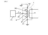
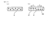
- the MI sensor element 1 of the present embodiment has a magnetometer 2 and a detection coil 3 wound around the magnetometer 2.
- the MI sensor element 1 is configured to output a voltage corresponding to the strength of the magnetic field acting on the magnetic sensor 2 from the detection coil 3 by passing a pulse current or a high frequency current through the magnetic sensor 2.
- a pulse current is passed through the magnetic sensor 2.
- the electromagnetic characteristics of the magnetic sensitive body 2 change due to a magnetic field acting from the outside.
- the magnetic sensor 2 is made of an amorphous wire.
- the magnetic sensor 2 is configured so that a pulse current flows in the axial direction thereof.
- the magnetic sensing body 2 has a first magnetic sensing portion 21 and a second magnetic sensing portion 22 configured so that pulse currents I1 and I2 flow in opposite directions to each other.
- the first magnetically sensitive portion 21 and the second magnetically sensitive portion 22 are integrally formed as one magnetically sensitive wire. That is, the magnetic sensitive body 2 is composed of one amorphous wire.
- the MI sensor element 1 has a central terminal 40 drawn from a central portion in the axial direction of the magnetometer 2.
- the MI sensor element 1 has a first terminal 41 drawn from one end of the first magnetic sensing portion 21 and a second terminal pulled out from one end of the second magnetic sensing portion 22. 42 and.
- the first terminal 41 and the second terminal 42 are respectively drawn out from both ends in the axial direction of the magnetic sensor 2.
- the portion from the portion where the central terminal 40 is pulled out to the portion where the first terminal 41 is pulled out is the first magnetic sensitive portion 21. Further, in the magnetic sensory body 2, the portion from the portion where the central terminal 40 is pulled out to the portion where the second terminal 42 is pulled out is the second magnetoreceptive portion 22.
- the detection coil 3 has a first coil portion 31 wound around the first magnetic sensing portion 21 and a second coil portion 32 wound around the second magnetic sensing portion 22.
- the first coil portion 31 and the second coil portion 32 are electrically connected in series with each other and have the same winding direction.
- Both ends of the detection coil 3 are connected to the output terminals 51 and 52, respectively.
- the end portion of the first coil portion 31 opposite to the second coil portion 32 is connected to one output terminal 51, and the end portion of the second coil portion 32 opposite to the first coil portion 31 is connected. , Is connected to the other output terminal 52.
- the first coil portion 31 and the second coil portion 32 have substantially the same number of turns.
- FIGS. 1 and 2 are explanatory views to the last, and the number of turns of the detection coil 3 is not particularly limited.
- each part of the detection coil 3 is inclined with respect to the circumferential direction of the magnetic sensitive body 2 when viewed from a direction orthogonal to the axial direction. However, in the figure, this inclination angle is shown to be larger than the actual one.
- the detection coil 3 is provided on the outer peripheral surface of the insulating layer that covers the outer periphery of the magnetic sensitive body 2.
- the detection coil 3 can be formed, for example, by plating.
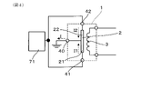
- the MI sensor element 1 has a substrate 6 on which a magnetometer 2 and a detection coil 3 are mounted. That is, the magnetic sensitive body 2 in the state where the detection coil 3 is wound as described above is fixed to the substrate 6 along the surface of the substrate 6.
- the board 6 is provided with a first terminal 41, a second terminal 42, a central terminal 40, and output terminals 51 and 52. These terminals may be formed on the surface of the substrate 6 by, for example, plating.
- connection wirings 411, 421, and 401 that electrically connect each of the first terminal 41, the second terminal 42, and the central terminal 40 and each part of the magnetic sensor 2 are also attached to the substrate 6 by plating or the like, for example. It is formed.
- connection wirings 511 and 521 that electrically connect the output terminals 51 and 52 and the detection coil 3 are also formed on the substrate 6 by plating or the like, for example.
- the MI sensor element 1 configured as described above is configured so that a pulse current can be applied to the magnetometer 2 from the central terminal 40. Then, in this case, the pulse current branches and flows into the first magnetic sensing portion 21 and the second magnetic sensing portion 22 in the central portion of the magnetic sensing body 2, and flows toward the first terminal 41 and the second terminal 42, respectively. Flows. That is, the pulse current I1 flowing through the first magnetic sensing portion 21 and the pulse current I2 flowing through the second magnetic sensing portion 22 flow in opposite directions to each other.
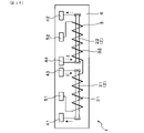
- Such a method of passing a pulse current through the magnetic sensor 2 can be realized, for example, by connecting a peripheral circuit simply shown in FIG. That is, the pulse power supply 71 that generates the pulse current is connected to the central terminal 40. Then, the first terminal 41 and the second terminal 42 are grounded, respectively. Then, by applying a pulse current from the pulse power supply 71 to the central portion of the magnetic sensor 2 via the central terminal 40, the first magnetic sensor 21 and the second magnetic sensor 22 of the magnetic sensor 2 are opposite to each other. Pulse currents I1 and I2 in the direction can be passed.
- the pulse current I1 flowing through the first magnetic sensing portion 21 and the pulse current I2 flowing through the second magnetic sensing portion 22 are made to have substantially the same magnitude. Further, the pulse current I1 and the pulse current I2 flow in synchronization with each other.
- the pulse current I1 and the pulse current I2 may be in opposite directions to each other. Therefore, as shown in FIG. 4, a pulse current can be applied to the magnetic sensor 2 from the first terminal 41 and the second terminal 42 toward the central terminal 40.
- the pulse power supply 71 can be connected to the first terminal 41 and the second terminal 42, and the central terminal 40 can be grounded, which is a peripheral circuit configuration.
- the peripheral circuits shown in FIGS. 3 and 4 are connected to the control unit, and the control unit controls the pulse power supply 71 and processes the output signal from the detection coil 3.
- the control unit can be configured by, for example, a microcomputer including a CPU, ROM, RAM, and the like.
- the magnetic sensor 2 has a first magnetic sensing portion 21 and a second magnetic sensing portion 22 configured so that pulse currents flow in opposite directions to each other. As a result, the vibration at the origin can be suppressed.
- the origin vibration is caused by the change in the magnetic field caused by the pulse current flowing through the magnetic sensor 2. That is, when the direction of the pulse current I flowing through the magnetic sensor 2 is only one direction as in the MI sensor element 9 of the comparative form shown in FIG. 5, the magnetic field change caused by the pulse current I occurs. Then, it is considered that an induced voltage is generated in the detection coil 3 due to this change in the magnetic field, so that an output is generated in the detection coil 3 even when an external magnetic field is not applied, that is, an origin vibration is generated. Be done.
- the MI sensor element 1 of the present embodiment is configured such that pulse currents I1 and I2 in opposite directions flow through the first magnetic sensing portion 21 and the second magnetic sensing portion 22 in the magnetic sensor 2. Has been done. This makes it possible to suppress the change in the magnetic field caused by the pulse current described above. That is, the magnetic field change caused by the pulse current I1 of the first magnetic sensing portion 21 and the magnetic field change caused by the pulse current I2 of the second magnetic sensing portion 22 cancel each other out. Therefore, in the MI sensor element 1 of the present embodiment, the magnetic field change caused by the pulse current is suppressed, and the origin vibration is suppressed.
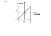
- the MI sensor element 1 has a certain relationship between the applied magnetic field and the output voltage (hereinafter, also referred to as input / output characteristics), and based on this, detects the magnitude of the applied magnetic field from the output voltage. Can be done (see Figure 7).
- the input / output characteristics show stable sensitivity in the predetermined output voltage range Rv
- the sensitivity decreases when the range is out of the range Rv. That is, the magnitude of the magnetic field that can be substantially measured is limited to the range Rh corresponding to the range Rv of the predetermined output voltage.
- the measurable magnetic field range Rh becomes narrow on the plus side or the minus side.
- the measurable range Rh of the magnetic field on the positive side becomes narrow.
- the strength of the magnetic field on one side is on the positive side, and the strength of the magnetic field in the opposite direction is on the negative side.
- the offset can be suppressed by suppressing the origin vibration as described above. Then, as shown in FIG. 7, by suppressing the offset, the measurable magnetic field range Rh can be widely secured on both the positive side and the negative side.
- the MI sensor element 1 utilizes the electromotive force generated in the detection coil 3 when the magnetic flux interlinking with the detection coil 3 (the magnetic flux in the axial direction of the magnetic sensor 2) is changed with time in the magnetic sensor 2. be.
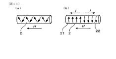
- the measurement principle using the MI sensor element 9 in the comparative form FIGS. 8 and 9.
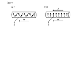
- the magnetic domain 2 has a magnetic domain structure in which a large number of magnetic domains are arranged in the axial direction. As shown in FIG. 8A, electron spins are formed in the circumferential direction in each magnetic domain, and the directions of the electron spins are opposite in the adjacent magnetic domains. In FIG. 8, the arrow drawn along the outer peripheral surface of the magnetic sensor 2 indicates the direction of the electron spin. The same applies to FIGS. 9 to 11.
- FIG. 9A when the external magnetic field H acts in the axial direction (that is, the magnetic sensing direction of the MI sensor element), the electron spin is tilted by the external magnetic field H.
- FIG. 9B when a pulse current is passed, the directions of the electron spins are aligned in the circumferential direction.
- the magnitude of the vector component of the electron spin in the direction of interlinking with the detection coil 3, that is, in the axial direction of the magnetic sensor 2 changes.
- a voltage is induced in the detection coil 3 by this change in magnetic flux.
- the magnitude of the magnetic field can be detected by the magnitude of the output voltage of the detection coil 3.
- the direction of the electron spin in the magnetic sensor 2 is partially reversed by applying the pulse current I.
- the pulse current I There is no change in the vector component of electron spin in the axial direction.
- the difference from the comparative form is that the directions of the electron spins when the pulse current I is applied are opposite in the first magnetic sensing portion 21 and the second magnetic sensing portion 22 in which the directions of the pulse currents are opposite. ..
- origin vibration may occur as described above. That is, in a state where an external magnetic field does not act as shown in FIG. 8B, a voltage may be induced in the detection coil 3 where an output voltage is not originally generated.
- the inventors considered that this vibration at the origin was caused by the change in the magnetic field caused by the application of the pulse current. As shown in FIG. 1, it is considered that the magnetic field generated by this pulse current is suppressed by canceling each other by flowing the pulse currents in opposite directions. Therefore, the inventors have succeeded in suppressing the origin vibration by adopting a configuration in which pulse currents flowing in opposite directions to the magnetic sensor 2 are passed (see an experimental example described later).
- the detection coil 3 has a first coil portion 31 and a second coil portion 32.
- the first coil portion 31 and the second coil portion 32 are electrically connected in series with each other and have the same winding direction. Thereby, the MI sensor element 1 can be easily and accurately manufactured.
- first magnetic sensing portion 21 and the second magnetic sensing portion 22 are integrally formed as one magnetic sensing wire. Therefore, the MI sensor element 1 can be manufactured easily and accurately. Further, since the difference in electromagnetic characteristics between the first magnetic sensing portion 21 and the second magnetic sensing portion 22 is unlikely to occur, it is easier to suppress the origin vibration.
- this embodiment is a form in which the first coil portion 31 and the second coil portion 32 are electrically connected to each other at the ends on opposite sides in the axial direction.
- the connection wiring 33 connecting the first coil portion 31 and the second coil portion 32 is formed, for example, on the surface of the substrate 6 by plating or the like.
- the first coil portion 31 and the second coil portion 32 are electrically connected to the output terminals 51 and 52 at the ends located close to each other in the axial direction.
- the effect confirmation test of the MI sensor element of the present disclosure was performed.
- the MI sensor element 1 shown in the second embodiment (FIG. 12) was prepared as the sample 1
- the MI sensor element 9 shown in the comparative embodiment (FIG. 5) was prepared as the sample 2 and the sample 3.
- the structure of the sample 2 and the sample 3 as the MI sensor element 9 is the same.
- the specific structure of the sample 2 and the sample 3 is the same as that of the sample 1 (that is, the second embodiment shown in FIG. 12) except that the central terminal 40 and the connection wiring 401 between the central terminal 40 and the magnetic sensor 2 are not provided. ..
- a pulse current having a predetermined magnitude was passed through the magnetic sensor 2.
- a pulse current was passed from the central terminal 40 toward the first terminal 41 and the second terminal 42.
- a pulse current was passed in the direction from one end to the other end of the magnetic sensor 2.
- the directions of the pulse current flowing through the sample 2 and the pulse current flowing through the sample 3 are opposite to each other.
- the pulse current flowing through each sample was the same magnitude and the same pulse waveform. That is, for the sample 1, the current value input to the central terminal 40 is twice the current value input to one end of the magnetic sensor 2 in the sample 2 and the sample 3.
- the voltage (output voltage) generated in the detection coil 3 in each sample was monitored.
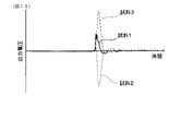
- the result is shown in FIG.
- the output voltage generated in the sample 1 is suppressed to less than half of the output voltage generated in the sample 2 and the sample 3. That is, in the sample 1, the origin vibration is suppressed.
- the output voltage of the sample 2 and the output voltage of the sample 3 have opposite codes. This is because the pulse current applied to the sample 2 and the direction of the pulse current applied to the sample 3 are opposite to each other, so that the direction of the magnetic field generated by these pulse currents is also opposite, and the origin vibration caused by this magnetic field is also reversed. It is thought that this is because it is in the opposite direction.
- the MI sensor element 1 of the second embodiment was able to suppress the origin vibration.
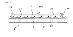
- this embodiment is a form in which the ground layer 61 is provided on the substrate 6.
- the grounding layer 61 is electrically grounded. Both ends of the magnetic sensor 2 are electrically connected to the ground layer 61.
- the description of the detection coil 3 is omitted.
- the ground layer 61 is formed in a plane on the substrate 6 so as to spread two-dimensionally.
- the ground layer 61 is formed so that the entire magnetic sensitive body 2 is arranged inside when viewed from the normal direction of the substrate 6.
- the magnetic sensitive body 2 when viewed from the normal direction of the substrate 6, the magnetic sensitive body 2, the output terminals 51 and 52, the central terminal 40, and the ground terminal 46 are arranged inside the contour of the ground layer 61. It is formed like this.
- the ground terminal 46 is a terminal that is electrically connected to the ground layer 61 and is exposed on the surface of the substrate 6. By connecting the ground terminal 46 to the external ground wiring, the ground layer 61 is grounded.
- the magnetic sensitive body 2 is electrically connected to the ground layer 61 at both ends thereof via a joining conductor 45. Further, the portions of the magnetic sensor 2 other than both ends are electrically insulated from the ground layer 61 by the insulating layer 62. Further, the central terminal 40 is electrically connected to the central portion of the magnetic sensitive body 2 via the connection wiring 401. Others are the same as in the second embodiment.
- the number of pulse current input terminals in the MI sensor element 1 can be reduced. Therefore, the manufacture of the MI sensor element 1 can be facilitated. Further, it is possible to reduce the portion where the pulse current path is asymmetrical except for the magnetic sensor 2. Thereby, the origin vibration can be suppressed more effectively. In addition, it has the same effect as that of the first embodiment.
- this embodiment is a form of the MI sensor element 1 in which the magnetometer 2 is divided into a plurality of arrangements. That is, in this embodiment, the first magnetic sensing portion 21 and the second magnetic sensing portion 22 are composed of individual magnetic sensing wires. The first magnetic sensing portion 21 and the second magnetic sensing portion 22 are arranged side by side in the axial direction. In particular, in this embodiment, the first magnetic sensing portion 21 and the second magnetic sensing portion 22 are arranged on the same straight line.
- first magnetic sensing portion 21 and the second magnetic sensing portion 22 have a pair of terminals connected to both ends thereof. That is, the first terminal 41 and the third terminal 43 are connected to both ends of the first magnetic sensing portion 21, respectively. Further, the second terminal 42 and the fourth terminal 44 are connected to both ends of the second magnetic sensing portion 22, respectively.
- the third terminal 43 is connected to the end of the first magnetic sensing portion 21 on the side closer to the second magnetic sensing portion 22, and the fourth terminal 44 is the first magnetic sensing portion 21 of the second magnetic sensing portion 22. It is connected to the end near the side.
- the first magnetic sensing portion 21 and the second magnetic sensing portion 22 are electrically independent of each other in the element. However, the first magnetic sensing portion 21 and the second magnetic sensing portion 22 may be electrically connected in the element.
- the first magnetic sensing portion 21 and the second magnetic sensing portion 22 can be magnetically sensitive wires having substantially the same diameter, length, and electromagnetic characteristics.
- the first magnetic sensing portion 21 and the second magnetic sensing portion 22 can be made into individual magnetic sensing wires by cutting one integrally manufactured magnetic sensing wire.
- a pulse current is passed from the third terminal 43 and the fourth terminal 44 to the first magnetic sensing portion 21 and the second magnetic sensing portion 22, respectively.
- pulse currents are passed from the first terminal 41 and the second terminal 42 to the first magnetic sensing portion 21 and the second magnetic sensing portion 22, respectively.
- pulse currents in opposite directions flow through the first magnetic sensing portion 21 and the second magnetic sensing portion 22.
- the application of the pulse current to the first magnetic sensing portion 21 and the second magnetic sensing portion 22 is performed in synchronization with each other. Others are the same as those in the first embodiment.
- a pulse current in the opposite direction can be reliably passed through the first magnetic sensing portion 21 and the second magnetic sensing portion 22.
- it has the same effect as that of the first embodiment.
- this embodiment is a form of the MI sensor element 1 in which the magnetometers 2 divided into a plurality of parts are arranged in parallel. That is, the first magnetic sensing portion 21 and the second magnetic sensing portion 22 are arranged in parallel. Further, in the detection coil 3, the first coil portion 31 and the second coil portion 32 are electrically connected in series with each other.
- the first magnetic sensing portion 21 and the second magnetic sensing portion 22 are arranged in parallel with each other and arranged side by side in a direction orthogonal to the axial direction.
- the first magnetic sensing portion 21 and the second magnetic sensing portion 22 are arranged at the same positions at both ends thereof in the axial direction. Others are the same as those in the first embodiment.
- pulse currents are passed from the third terminal 43 and the fourth terminal 44 to the first magnetic sensing portion 21 and the second magnetic sensing portion 22, respectively.
- pulse currents are passed from the first terminal 41 and the second terminal 42 to the first magnetic sensing portion 21 and the second magnetic sensing portion 22, respectively.
- pulse currents in opposite directions flow through the first magnetic sensing portion 21 and the second magnetic sensing portion 22.
- the application of the pulse current to the first magnetic sensing portion 21 and the second magnetic sensing portion 22 is performed in synchronization with each other.
- the axial length of the magnetic sensor 2 can be shortened. Therefore, it is possible to improve the sensing resolution of the MI sensor element 1 in the axial direction. In addition, the size of the MI sensor element 1 in the axial direction can be easily reduced. Others are the same as in the fourth embodiment.
- this embodiment is a form of the MI sensor element 1 in which the detection coil 3 is wound around the first magnetic sensing portion 21 and the second magnetic sensing portion 22 arranged in parallel. Also in this embodiment, pulse currents in opposite directions flow through the first magnetic sensing portion 21 and the second magnetic sensing portion 22. A pair of output terminals 51 and 52 are connected to both ends of the detection coil 3.
- an output voltage corresponding to the magnetic field is output from both ends of the detection coil 3. That is, the output voltage is output between the pair of output terminals 51 and 52.
- Others are the same as in the fifth embodiment.
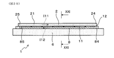
- this embodiment is a form of a magnetoimpedance sensor element 10 having a parallel conductor 8.
- the MI sensor element 10 of this embodiment has a magnetometer 2, a parallel conductor 8, and a detection coil 3.
- the electromagnetic characteristics of the magnetic sensitive body 2 change due to a magnetic field acting from the outside.
- the parallel conductor 8 is a conductor arranged in parallel with the magnetic sensitive body 2.
- the detection coil 3 is wound around the magnetic sensitive body 2 and the parallel conductor 8.
- the detection coil 3 is configured to output a voltage corresponding to the strength of the magnetic field acting on the magnetic sensor 2 by passing a pulse current or a high frequency current through the magnetic sensor 2.
- the parallel conductor 8 is configured to allow a pulse current or high frequency current to flow in the direction opposite to the pulse current or high frequency current flowing through the magnetic sensor 2. Further, in this embodiment, a pulse current is passed through the magnetic sensitive body 2 and the parallel conductor 8.
- the magnetic sensitive body 2 is a magnetic sensitive wire and is made of an amorphous wire.
- the parallel conductor 8 is connected in series with the magnetic sensitive body 2. That is, one end 84 of the parallel conductor 8 is electrically connected to one end 24 of the magnetic sensitive body 2.
- the parallel conductor 8 is formed on the surface of the substrate 6.
- the parallel conductor 8 may be formed on the surface of the substrate 6 by, for example, copper plating.
- the magnetic sensitive body 2 is arranged on the surface of the parallel conductor 8 on the opposite side of the substrate 6 via the insulating layer 11.
- an insulating layer 11 made of resin is formed on the surface of the parallel conductor 8.
- the detection coil 3 is omitted.
- the magnetic sensor 2 has an insulating layer 11 on the surface of the parallel conductor 8 so that the longitudinal direction (axial direction) of the magnetic sensor 2 and the longitudinal direction of the parallel conductor 8 coincide with each other. It is installed via. However, one end 24 of the magnetic sensitive body 2 and one end 84 of the parallel conductor 8 are connected at the end connecting portion 12. As shown in FIG. 19, the other end 25 of the magnetic sensor 2 is electrically connected to the magnetic sensor terminal 410 formed on the substrate 6, and the other end 85 of the parallel conductor 8 is for the conductor formed on the substrate 6. It is electrically connected to the terminal 420.
- the MI sensor element 10 has a magnetometer terminal 410 drawn from an end portion 25 on the opposite side of the end portion connecting portion 12 in the magnetometer body 2 and an end portion on the side opposite to the end portion connecting portion 12 in the parallel conductor 8. It has a conductor terminal 420 drawn from 85.
- the magnitude of the pulse current or high-frequency current flowing through the parallel conductor 8 is the same as the magnitude of the pulse current or high-frequency current flowing through the magnetic sensor 2. Therefore, for example, the thickness of the parallel conductor 8 can be adjusted to appropriately adjust the electric resistance of the parallel conductor 8.
- the parallel conductor 8 is not adjacent to each other in a part of the magnetic sensor 2, but the magnetic sensor 2 and the parallel conductor 8 are adjacent to each other over substantially the entire longitudinal direction (for example, 90% or more). Have been placed.
- the portion of the magnetic sensor 2 where the parallel conductors 8 are not adjacent to each other is a portion where the detection coil 3 is not wound.
- the detection coil 3 is wound so as to surround both the magnetic sensor 2 and the parallel conductor 8.
- the detection coil 3 has two coil portions 310 and 320.
- the two coil portions 310 and 320 are electrically connected to each other by connecting wirings 330 at the opposite ends of the magnetic sensitive body 2 in the axial direction.
- the two coil portions 310 and 320 are electrically connected to the output terminals 51 and 52 at the ends located close to each other in the axial direction.
- the parallel conductor 8 is arranged adjacent to the magnetic sensitive body 2 in one direction orthogonal to the axial direction of the magnetic sensitive body 2.
- the magnetic sensor 2 and the parallel conductor 8 are arranged adjacent to each other in the normal direction of the substrate 6.
- a pulse current or a high frequency current flows in the parallel conductor 8 in the direction opposite to the pulse current or the high frequency current flowing in the magnetic sensor 2.
- the origin vibration can be suppressed as in the first embodiment.
- the pulse current or high frequency current is appropriately referred to as a pulse current or the like.
- the change in the magnetic field caused by the pulse current or the like flowing through the magnetic sensor 2 can be canceled by the change in the magnetic field caused by the pulse current or the like flowing through the parallel conductor 8. If there is a difference between the magnitude of the pulse current or the like flowing through the parallel conductor 8 and the magnitude of the pulse current or the like flowing through the magnetic sensor 2, the above magnetic field change cannot be completely canceled, but it is suppressed. Can be done. Therefore, the origin vibration can be suppressed at the output of the MI sensor element 10.
- the origin vibration can be suppressed as described above by providing the parallel conductor 8. Therefore, the origin vibration can be suppressed without hindering the miniaturization of the MI sensor element 10. That is, in the case of this embodiment, it is not necessary to add or lengthen the magnetic sensor 2 in order to suppress the origin vibration.
- the parallel conductor 8 can be formed by, for example, a general wiring patterning technique using photolithography and plating. Therefore, the origin vibration can be suppressed without particularly complicating the manufacturing method of the MI sensor element 10.
- the parallel conductor 8 is connected in series with the magnetic sensitive body 2. This makes it easier to synchronize the pulse current or high-frequency current magnetic body flowing through the parallel conductor 8 with the pulse current or high-frequency current flowing through the magnetic sensor 2. Therefore, the suppression of the origin vibration can be realized more easily.
- the parallel conductor 8 is arranged adjacent to the magnetic sensitive body 2 in one direction orthogonal to the axial direction of the magnetic sensitive body 2. As a result, it is possible to suppress the disturbance of the current distribution in the parallel conductor 8. That is, when the frequency of the flowing pulse current or the like increases, the impedance of the insulating layer 11 arranged between the magnetic sensor 2 and the parallel conductor 8 tends to decrease. Then, if the parallel conductors are arranged adjacent to each other on the entire circumference of the magnetic sensitive body, the influence of the impedance reduction of the insulating layer becomes large, and the current distribution flowing through the parallel conductors tends to be disturbed.
- the parallel conductors 8 are arranged adjacent to each other only in one direction orthogonal to the axial direction of the magnetic sensor 2, the influence of the impedance decrease of the insulating layer 11 can be suppressed. As a result, it is possible to more effectively suppress the vibration at the origin. In addition, it has the same effect as that of the first embodiment.
- the magnetic sensor 2 and the parallel conductor 8 may be arranged so as to be arranged in a direction parallel to the surface of the substrate 6 (not shown). Further, as still another modification of the seventh embodiment, the magnetic sensor 2 and the parallel conductor 8 may be configured not to be electrically connected to each other (not shown). Then, in this case, a pulse current or the like can be applied to each of the magnetic sensor 2 and the parallel conductor 8 by a method according to the fourth embodiment. It should be noted that the parallel conductor and the magnetic sensor do not necessarily have to be completely parallel, and may be slightly inclined to each other as long as they are substantially parallel.
- the present invention is not limited to each of the above embodiments, and can be applied to various embodiments without departing from the gist thereof.
Abstract
Description
上記感磁体は、互いに逆向きに上記パルス電流又は高周波電流が流れるよう構成された第1感磁部と第2感磁部とを有する、マグネトインピーダンスセンサ素子にある。 The first aspect of the present invention has a magnetic sensor whose electromagnetic characteristics are changed by a magnetic field acting from the outside and a detection coil wound around the magnetic sensor, and applies a pulse current or a high frequency current to the magnetic sensor. A magnetic impedance sensor element configured to output a voltage corresponding to the strength of the magnetic field acting on the magnetic sensor from the detection coil by flowing the current.
The magnetic sensor is a magnetoimpedance sensor element having a first magnetic sensitive portion and a second magnetic sensitive portion configured to allow the pulse current or high frequency current to flow in opposite directions to each other.
該感磁体と平行に配置された平行導体と、
上記感磁体及び平行導体に巻回された検出コイルと、を有し、
上記感磁体にパルス電流又は高周波電流を流すことにより、上記感磁体に作用する磁場の強さに対応した電圧を上記検出コイルから出力するよう構成され、
上記平行導体には、上記感磁体に流れる上記パルス電流又は高周波電流と逆向きに、パルス電流又は高周波電流が流れるよう構成されている、マグネトインピーダンスセンサ素子にある。 A second aspect of the present invention is a magnetic sensitive body whose electromagnetic characteristics are changed by a magnetic field acting from the outside.
A parallel conductor arranged parallel to the magnetic sensor,
It has a detection coil wound around the magnetic sensor and a parallel conductor, and has.
By passing a pulse current or a high-frequency current through the magnetic sensor, a voltage corresponding to the strength of the magnetic field acting on the magnetic sensor is output from the detection coil.
The parallel conductor is a magnetic impedance sensor element configured to allow a pulse current or high frequency current to flow in the direction opposite to the pulse current or high frequency current flowing through the magnetic sensor.
また、上記感磁体は、例えば、アモルファス磁性体からなる線状部材である、アモルファスワイヤにて構成することができる。そして、感磁体には、その軸方向にパルス電流又は高周波電流が流れるように構成されている。 The magnetoimpedance element of the above aspect can be used, for example, in an electronic compass, a foreign matter detection sensor, a magnetic positioning system, or the like.
Further, the magnetic sensitive material can be made of, for example, an amorphous wire which is a linear member made of an amorphous magnetic material. The magnetic sensor is configured so that a pulse current or a high-frequency current flows in the axial direction thereof.
MIセンサ素子の実施形態につき、図1~図11を参照して説明する。
本形態のMIセンサ素子1は、図1に示すごとく、感磁体2と、感磁体2に巻回された検出コイル3と、を有する。そして、MIセンサ素子1は、感磁体2にパルス電流又は高周波電流を流すことにより、感磁体2に作用する磁場の強さに対応した電圧を検出コイル3から出力するよう構成されている。本形態においては、感磁体2にはパルス電流を流す。 (Embodiment 1)
An embodiment of the MI sensor element will be described with reference to FIGS. 1 to 11.
As shown in FIG. 1, the
図1に示すごとく、感磁体2は、互いに逆向きにパルス電流I1、I2が流れるよう構成された第1感磁部21と第2感磁部22とを有する。 The electromagnetic characteristics of the magnetic
As shown in FIG. 1, the
上記マグネトインピーダンスセンサ素子1において、感磁体2は、互いに逆向きにパルス電流が流れるよう構成された第1感磁部21と第2感磁部22とを有する。これにより、原点振動を抑制することができる。 Next, the action and effect of this embodiment will be described.
In the
そもそも、MIセンサ素子1は、感磁体2において、検出コイル3に鎖交する磁束(感磁体2の軸方向の磁束)を時間変化させたときに検出コイル3に生じる起電力を利用するものである。分かり易さのために、まず、比較形態(図5)のMIセンサ素子9を用いた測定原理を、図8、図9を参照して説明する。 Further, even when pulse currents in opposite directions are passed through the
In the first place, the
したがって、感磁体2に、互いに逆向きのパルス電流Iを印加しても、外部磁場Hの検出感度自体に影響を及ぼすことはない。 Then, as shown in FIGS. 11A and 11B, even when the pulse current I is applied in a state where the external magnetic field H is acting in the axial direction, the direction of interlinking with the
Therefore, even if the pulse currents I in opposite directions are applied to the
本形態は、図12に示すごとく、第1コイル部31と第2コイル部32とを、互いに、軸方向の反対側の端部同士において、電気的に接続した形態である。
第1コイル部31と第2コイル部32とを接続する接続配線33は、例えば、基板6の表面に、メッキ等にて形成されている。そして、第1コイル部31及び第2コイル部32は、軸方向において互いに近い位置の端部において、出力端子51、52のそれぞれに電気的に接続されている。 (Embodiment 2)
As shown in FIG. 12, this embodiment is a form in which the
The
本形態においても、実施形態1と同様の作用効果を有する。 Others are the same as those in the first embodiment. In addition, among the codes used in the second and subsequent embodiments, the same codes as those used in the above-mentioned embodiments represent the same components and the like as those in the above-mentioned embodiments, unless otherwise specified.
Also in this embodiment, it has the same effect as that of the first embodiment.
本例においては、図13に示すごとく、本開示のMIセンサ素子の効果確認試験を行った。
試料としては、実施形態2(図12)に示したMIセンサ素子1を、試料1、比較形態(図5)に示したMIセンサ素子9を、試料2、試料3として用意した。
試料2と試料3とは、MIセンサ素子9としての構造は同じである。また、試料2及び試料3の具体的な構造は、中央端子40及びこれと感磁体2との接続配線401がない以外は、試料1(すなわち、図12に示す実施形態2)と同様である。 (Experimental example)
In this example, as shown in FIG. 13, the effect confirmation test of the MI sensor element of the present disclosure was performed.
As a sample, the
The structure of the
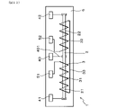
本形態は、図14、図15に示すごとく、基板6に接地層61を設けた形態である。
接地層61は、電気的に接地される。そして、感磁体2の両端部は、接地層61に電気的に接続されている。なお、図15においては、検出コイル3の記載を省略している。 (Embodiment 3)
As shown in FIGS. 14 and 15, this embodiment is a form in which the
The
その他は、実施形態2と同様である。 The magnetic
Others are the same as in the second embodiment.
その他、実施形態1と同様の作用効果を有する。 In this embodiment, the number of pulse current input terminals in the
In addition, it has the same effect as that of the first embodiment.
本形態は、図16に示すごとく、感磁体2を複数に分けて配置したMIセンサ素子1の形態である。
すなわち、本形態においては、第1感磁部21と第2感磁部22とを、個別の感磁ワイヤにて構成している。そして、第1感磁部21と第2感磁部22とは、軸方向に並んで配置されている。特に、本形態においては、同一直線上に、第1感磁部21と第2感磁部22とが配置されている。 (Embodiment 4)
As shown in FIG. 16, this embodiment is a form of the
That is, in this embodiment, the first
その他は、実施形態1と同様である。 In this embodiment, for example, a pulse current is passed from the
Others are the same as those in the first embodiment.
その他、実施形態1と同様の作用効果を有する。 In this embodiment, a pulse current in the opposite direction can be reliably passed through the first
In addition, it has the same effect as that of the first embodiment.
本形態は、図17に示すごとく、複数に分割した感磁体2を並列配置したMIセンサ素子1の形態である。
すなわち、第1感磁部21と第2感磁部22とを、並列配置している。また、検出コイル3における、第1コイル部31と第2コイル部32とは、互いに電気的に直列接続されている。 (Embodiment 5)
As shown in FIG. 17, this embodiment is a form of the
That is, the first
その他は、実施形態1と同様である。 The first
Others are the same as those in the first embodiment.
その他は、実施形態1と同様である。 It is also possible to calculate and synthesize the output signals generated from the respective coil units without directly connecting the
Others are the same as those in the first embodiment.
その他、実施形態4と同様である。 In this embodiment, the axial length of the
Others are the same as in the fourth embodiment.
本形態は、図18に示すごとく、並列配置した第1感磁部21及び第2感磁部22の周りに、検出コイル3を巻回したMIセンサ素子1の形態である。
本形態においても、第1感磁部21と第2感磁部22とには、互いに逆向きのパルス電流が流れるようにする。検出コイル3の両端に、一対の出力端子51、52が接続されている。 (Embodiment 6)
As shown in FIG. 18, this embodiment is a form of the
Also in this embodiment, pulse currents in opposite directions flow through the first
その他は、実施形態5と同様である。 In this embodiment, an output voltage corresponding to the magnetic field is output from both ends of the
Others are the same as in the fifth embodiment.
その他、実施形態5と同様の作用効果を有する。 In this embodiment, it is possible to facilitate further miniaturization of the
In addition, it has the same effect as that of the fifth embodiment.
本形態は、図19~図21に示すごとく、平行導体8を有するマグネトインピーダンスセンサ素子10の形態である。
本形態のMIセンサ素子10は、感磁体2と平行導体8と検出コイル3とを有する。感磁体2は、外部から作用する磁場により電磁特性が変化する。平行導体8は、感磁体2と平行に配置された導体である。検出コイル3は、感磁体2及び平行導体8に巻回されている。 (Embodiment 7)
As shown in FIGS. 19 to 21, this embodiment is a form of a magnetoimpedance sensor element 10 having a
The MI sensor element 10 of this embodiment has a
その他、実施形態1と同様の作用効果を有する。 Further, the
In addition, it has the same effect as that of the first embodiment.
また、実施形態7のさらに他の変形形態として、感磁体2と平行導体8とを互いに電気的に接続しない構成とすることもできる(図示略)。そして、この場合、実施形態4に準ずる方法にて、感磁体2と平行導体8とのそれぞれに、パルス電流等の印加を行うよう構成することができる。
なお、平行導体と感磁体とは、完全に平行である必要は必ずしもなく、実質的に平行であれば、互いに若干傾斜していてもよい。 As a modification of the
Further, as still another modification of the seventh embodiment, the
It should be noted that the parallel conductor and the magnetic sensor do not necessarily have to be completely parallel, and may be slightly inclined to each other as long as they are substantially parallel.
Claims (8)
- 外部から作用する磁場により電磁特性が変化する感磁体と、該感磁体に巻回された検出コイルと、を有し、上記感磁体にパルス電流又は高周波電流を流すことにより、上記感磁体に作用する磁場の強さに対応した電圧を上記検出コイルから出力するよう構成されたマグネトインピーダンスセンサ素子であって、
上記感磁体は、互いに逆向きに上記パルス電流又は高周波電流が流れるよう構成された第1感磁部と第2感磁部とを有する、マグネトインピーダンスセンサ素子。 It has a magnetic sensor whose electromagnetic characteristics change due to a magnetic field acting from the outside and a detection coil wound around the magnetic sensor, and acts on the magnetic sensor by passing a pulse current or a high-frequency current through the magnetic sensor. It is a magnetic impedance sensor element configured to output a voltage corresponding to the strength of the magnetic field from the detection coil.
The magnetic sensory body is a magnetoimpedance sensor element having a first magnetically sensitive portion and a second magnetically sensitive portion configured so that the pulse current or high frequency current flows in opposite directions to each other. - 上記検出コイルは、上記第1感磁部に巻回された第1コイル部と、上記第2感磁部に巻回された第2コイル部とを有し、上記第1コイル部と上記第2コイル部とは、互いに電気的に直列接続されると共に、巻回向きが同じである、請求項1に記載のマグネトインピーダンスセンサ素子。 The detection coil has a first coil portion wound around the first magnetic sensing portion and a second coil portion wound around the second magnetic sensing portion, and has the first coil portion and the first coil portion. The magnetoimpedance sensor element according to claim 1, wherein the two coil portions are electrically connected in series with each other and have the same winding direction.
- 上記第1感磁部と上記第2感磁部とは、一本の感磁ワイヤとして一体的に形成されている、請求項2に記載のマグネトインピーダンスセンサ素子。 The magnetoimpedance sensor element according to claim 2, wherein the first magnetically sensitive portion and the second magnetically sensitive portion are integrally formed as one magnetically sensitive wire.
- 上記感磁体及び上記検出コイルを搭載した基板を有し、該基板には、接地された接地層が形成されており、上記感磁体の両端部は、上記接地層に電気的に接続されている、請求項3に記載のマグネトインピーダンスセンサ素子。 It has a substrate on which the magnetic sensor and the detection coil are mounted, and a grounded ground layer is formed on the substrate, and both ends of the magnetic sensor are electrically connected to the ground layer. , The magnetic impedance sensor element according to claim 3.
- 上記第1感磁部の一端から引き出された第1端子と、上記第2感磁部の一端から引き出された第2端子と、を有し、上記第1端子と上記第2端子とは、互いに電気的に独立している、請求項1~3のいずれか一項に記載のマグネトインピーダンスセンサ素子。 It has a first terminal drawn from one end of the first magnetic sensing portion and a second terminal drawn out from one end of the second magnetic sensing portion, and the first terminal and the second terminal are referred to as each other. The magnetoimpedance sensor element according to any one of claims 1 to 3, which is electrically independent of each other.
- 外部から作用する磁場により電磁特性が変化する感磁体と、
該感磁体と平行に配置された平行導体と、
上記感磁体及び平行導体に巻回された検出コイルと、を有し、
上記感磁体にパルス電流又は高周波電流を流すことにより、上記感磁体に作用する磁場の強さに対応した電圧を上記検出コイルから出力するよう構成され、
上記平行導体には、上記感磁体に流れる上記パルス電流又は高周波電流と逆向きに、パルス電流又は高周波電流が流れるよう構成されている、マグネトインピーダンスセンサ素子。 A magnetic sensor whose electromagnetic characteristics change due to an external magnetic field,
A parallel conductor arranged parallel to the magnetic sensor,
It has a detection coil wound around the magnetic sensor and a parallel conductor, and has.
By passing a pulse current or a high-frequency current through the magnetic sensor, a voltage corresponding to the strength of the magnetic field acting on the magnetic sensor is output from the detection coil.
A magnetic impedance sensor element configured such that a pulse current or a high frequency current flows in the parallel conductor in the direction opposite to the pulse current or the high frequency current flowing in the magnetic sensor. - 上記平行導体は、上記感磁体と直列接続されている、請求項6に記載のマグネトインピーダンスセンサ素子。 The magnetoimpedance sensor element according to claim 6, wherein the parallel conductor is connected in series with the magnetic sensor.
- 上記平行導体は、上記感磁体に対して、該感磁体の軸方向に直交する一方向に隣接配置されている、請求項6又は7に記載のマグネトインピーダンスセンサ素子。 The magnetoimpedance sensor element according to claim 6 or 7, wherein the parallel conductor is adjacent to the magnetic sensor in one direction orthogonal to the axial direction of the magnetic sensor.
Priority Applications (4)
| Application Number | Priority Date | Filing Date | Title |
|---|---|---|---|
| JP2022553759A JPWO2022070842A1 (en) | 2020-09-30 | 2021-09-10 | |
| EP21875144.4A EP4191694A4 (en) | 2020-09-30 | 2021-09-10 | Magneto-impedance sensor element |
| US18/044,136 US20230333177A1 (en) | 2020-09-30 | 2021-09-10 | Magneto-impedance sensor element |
| CN202180055984.1A CN116034648A (en) | 2020-09-30 | 2021-09-10 | Magneto-impedance sensor element |
Applications Claiming Priority (2)
| Application Number | Priority Date | Filing Date | Title |
|---|---|---|---|
| JP2020-165692 | 2020-09-30 | ||
| JP2020165692 | 2020-09-30 |
Publications (1)
| Publication Number | Publication Date |
|---|---|
| WO2022070842A1 true WO2022070842A1 (en) | 2022-04-07 |
Family
ID=80950390
Family Applications (1)
| Application Number | Title | Priority Date | Filing Date |
|---|---|---|---|
| PCT/JP2021/033344 WO2022070842A1 (en) | 2020-09-30 | 2021-09-10 | Magneto-impedance sensor element |
Country Status (5)
| Country | Link |
|---|---|
| US (1) | US20230333177A1 (en) |
| EP (1) | EP4191694A4 (en) |
| JP (1) | JPWO2022070842A1 (en) |
| CN (1) | CN116034648A (en) |
| WO (1) | WO2022070842A1 (en) |
Cited By (1)
| Publication number | Priority date | Publication date | Assignee | Title |
|---|---|---|---|---|
| WO2023063036A1 (en) * | 2021-10-15 | 2023-04-20 | 愛知製鋼株式会社 | Magnetic detecting device |
Citations (11)
| Publication number | Priority date | Publication date | Assignee | Title |
|---|---|---|---|---|
| JP2000284030A (en) * | 1999-03-31 | 2000-10-13 | Minebea Co Ltd | Magnetic sensor element |
| US20050146326A1 (en) * | 2002-01-15 | 2005-07-07 | Xiaoping Li | Variable permeability magnetic field sensor and method |
| JP2006300906A (en) * | 2005-04-25 | 2006-11-02 | Aichi Steel Works Ltd | Magneto-impedance sensor element |
| WO2009044820A1 (en) * | 2007-10-02 | 2009-04-09 | Aichi Steel Corporation | Magneto-impedance element and magneto-impedance sensor |
| JP2009236803A (en) * | 2008-03-28 | 2009-10-15 | Aichi Steel Works Ltd | Magnet impedance sensor element |
| CN101738587A (en) * | 2008-11-24 | 2010-06-16 | 于文杰 | Micro-magnetic sensor |
| JP2012078198A (en) | 2010-10-01 | 2012-04-19 | Aichi Steel Works Ltd | Magneto impedance sensor element and manufacturing method of the same |
| JP2016151413A (en) * | 2015-02-16 | 2016-08-22 | マグネデザイン株式会社 | Superhigh sensitivity micro magnetic sensor |
| JP2018148189A (en) * | 2017-03-01 | 2018-09-20 | ナノコイル株式会社 | Method for manufacturing nanocoil type GSR sensor element |
| WO2018225454A1 (en) * | 2017-06-05 | 2018-12-13 | 朝日インテック株式会社 | Gsr sensor element |
| JP6839399B1 (en) * | 2020-09-29 | 2021-03-10 | マグネデザイン株式会社 | Magnetic field detection element |
Family Cites Families (4)
| Publication number | Priority date | Publication date | Assignee | Title |
|---|---|---|---|---|
| US5889403A (en) * | 1995-03-31 | 1999-03-30 | Canon Denshi Kabushiki Kaisha | Magnetic detecting element utilizing magnetic impedance effect |
| JP3360168B2 (en) * | 1999-04-08 | 2002-12-24 | ミネベア株式会社 | Magnetic impedance element |
| JP2001004726A (en) * | 1999-06-22 | 2001-01-12 | Tdk Corp | Magnetic field sensor |
| JP6240994B1 (en) * | 2016-12-15 | 2017-12-06 | 朝日インテック株式会社 | 3D magnetic field detection element and 3D magnetic field detection device |
-
2021
- 2021-09-10 WO PCT/JP2021/033344 patent/WO2022070842A1/en active Application Filing
- 2021-09-10 EP EP21875144.4A patent/EP4191694A4/en active Pending
- 2021-09-10 US US18/044,136 patent/US20230333177A1/en active Pending
- 2021-09-10 CN CN202180055984.1A patent/CN116034648A/en active Pending
- 2021-09-10 JP JP2022553759A patent/JPWO2022070842A1/ja active Pending
Patent Citations (11)
| Publication number | Priority date | Publication date | Assignee | Title |
|---|---|---|---|---|
| JP2000284030A (en) * | 1999-03-31 | 2000-10-13 | Minebea Co Ltd | Magnetic sensor element |
| US20050146326A1 (en) * | 2002-01-15 | 2005-07-07 | Xiaoping Li | Variable permeability magnetic field sensor and method |
| JP2006300906A (en) * | 2005-04-25 | 2006-11-02 | Aichi Steel Works Ltd | Magneto-impedance sensor element |
| WO2009044820A1 (en) * | 2007-10-02 | 2009-04-09 | Aichi Steel Corporation | Magneto-impedance element and magneto-impedance sensor |
| JP2009236803A (en) * | 2008-03-28 | 2009-10-15 | Aichi Steel Works Ltd | Magnet impedance sensor element |
| CN101738587A (en) * | 2008-11-24 | 2010-06-16 | 于文杰 | Micro-magnetic sensor |
| JP2012078198A (en) | 2010-10-01 | 2012-04-19 | Aichi Steel Works Ltd | Magneto impedance sensor element and manufacturing method of the same |
| JP2016151413A (en) * | 2015-02-16 | 2016-08-22 | マグネデザイン株式会社 | Superhigh sensitivity micro magnetic sensor |
| JP2018148189A (en) * | 2017-03-01 | 2018-09-20 | ナノコイル株式会社 | Method for manufacturing nanocoil type GSR sensor element |
| WO2018225454A1 (en) * | 2017-06-05 | 2018-12-13 | 朝日インテック株式会社 | Gsr sensor element |
| JP6839399B1 (en) * | 2020-09-29 | 2021-03-10 | マグネデザイン株式会社 | Magnetic field detection element |
Non-Patent Citations (1)
| Title |
|---|
| See also references of EP4191694A4 |
Cited By (1)
| Publication number | Priority date | Publication date | Assignee | Title |
|---|---|---|---|---|
| WO2023063036A1 (en) * | 2021-10-15 | 2023-04-20 | 愛知製鋼株式会社 | Magnetic detecting device |
Also Published As
| Publication number | Publication date |
|---|---|
| EP4191694A1 (en) | 2023-06-07 |
| CN116034648A (en) | 2023-04-28 |
| JPWO2022070842A1 (en) | 2022-04-07 |
| EP4191694A4 (en) | 2024-01-10 |
| US20230333177A1 (en) | 2023-10-19 |
Similar Documents
| Publication | Publication Date | Title |
|---|---|---|
| JP4655162B2 (en) | Magneto-impedance element and magneto-impedance sensor | |
| JP6069129B2 (en) | Enhancement of planar RF sensor technology | |
| EP2562550B1 (en) | Method for detecting magnetic field generated by a current to estimate the amount of current | |
| JP6107942B2 (en) | Magnetic current sensor and current measuring method | |
| JP6255902B2 (en) | Magnetic field detector | |
| EP1300687A2 (en) | Device for measuring magnetic fields | |
| US9678177B2 (en) | Magnetic sensor device for suppressing magnetic saturation | |
| JP5234459B2 (en) | Current sensor | |
| KR20040079932A (en) | Integrated magnetic field strap for signal isolator | |
| WO2022070842A1 (en) | Magneto-impedance sensor element | |
| JP6384677B2 (en) | Current sensor | |
| WO2015190155A1 (en) | Current sensor | |
| JP2008203238A (en) | Current detecting device | |
| WO2017213003A1 (en) | Magneto-impedance sensor | |
| JP6394740B2 (en) | Magnetic field detector | |
| JP6819164B2 (en) | Magnetic field detector | |
| JP2016145745A (en) | Magnetic sensor | |
| JP2021148625A (en) | Magnetic sensor device | |
| JP2010256316A (en) | Current sensor | |
| JP5556603B2 (en) | Magnetic isolator | |
| US11333723B2 (en) | Magnetic sensor | |
| US7355391B2 (en) | Electromechanical conversion device | |
| RU2495514C1 (en) | Magnetoresistive sensor | |
| WO2011155526A1 (en) | Flux gate sensor, electronic direction finder using same, and current meter | |
| WO2015125233A1 (en) | Current detection device |
Legal Events
| Date | Code | Title | Description |
|---|---|---|---|
| 121 | Ep: the epo has been informed by wipo that ep was designated in this application |
Ref document number: 21875144 Country of ref document: EP Kind code of ref document: A1 |
|
| ENP | Entry into the national phase |
Ref document number: 2022553759 Country of ref document: JP Kind code of ref document: A |
|
| WWE | Wipo information: entry into national phase |
Ref document number: 2021875144 Country of ref document: EP |
|
| ENP | Entry into the national phase |
Ref document number: 2021875144 Country of ref document: EP Effective date: 20230227 |
|
| NENP | Non-entry into the national phase |
Ref country code: DE |