WO2022065202A1 - 半導体装置 - Google Patents
半導体装置 Download PDFInfo
- Publication number
- WO2022065202A1 WO2022065202A1 PCT/JP2021/034165 JP2021034165W WO2022065202A1 WO 2022065202 A1 WO2022065202 A1 WO 2022065202A1 JP 2021034165 W JP2021034165 W JP 2021034165W WO 2022065202 A1 WO2022065202 A1 WO 2022065202A1
- Authority
- WO
- WIPO (PCT)
- Prior art keywords
- insulating film
- region
- main surface
- trench
- separation
- Prior art date
- Legal status (The legal status is an assumption and is not a legal conclusion. Google has not performed a legal analysis and makes no representation as to the accuracy of the status listed.)
- Ceased
Links
Images




















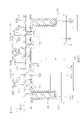


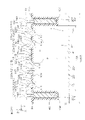

Classifications
-
- H—ELECTRICITY
- H10—SEMICONDUCTOR DEVICES; ELECTRIC SOLID-STATE DEVICES NOT OTHERWISE PROVIDED FOR
- H10W—GENERIC PACKAGES, INTERCONNECTIONS, CONNECTORS OR OTHER CONSTRUCTIONAL DETAILS OF DEVICES COVERED BY CLASS H10
- H10W10/00—Isolation regions in semiconductor bodies between components of integrated devices
- H10W10/10—Isolation regions comprising dielectric materials
- H10W10/17—Isolation regions comprising dielectric materials formed using trench refilling with dielectric materials, e.g. shallow trench isolations
-
- H—ELECTRICITY
- H10—SEMICONDUCTOR DEVICES; ELECTRIC SOLID-STATE DEVICES NOT OTHERWISE PROVIDED FOR
- H10D—INORGANIC ELECTRIC SEMICONDUCTOR DEVICES
- H10D30/00—Field-effect transistors [FET]
- H10D30/01—Manufacture or treatment
- H10D30/021—Manufacture or treatment of FETs having insulated gates [IGFET]
- H10D30/0221—Manufacture or treatment of FETs having insulated gates [IGFET] having asymmetry in the channel direction, e.g. lateral high-voltage MISFETs having drain offset region or extended-drain MOSFETs [EDMOS]
-
- H—ELECTRICITY
- H10—SEMICONDUCTOR DEVICES; ELECTRIC SOLID-STATE DEVICES NOT OTHERWISE PROVIDED FOR
- H10D—INORGANIC ELECTRIC SEMICONDUCTOR DEVICES
- H10D30/00—Field-effect transistors [FET]
- H10D30/01—Manufacture or treatment
- H10D30/021—Manufacture or treatment of FETs having insulated gates [IGFET]
- H10D30/028—Manufacture or treatment of FETs having insulated gates [IGFET] of double-diffused metal oxide semiconductor [DMOS] FETs
- H10D30/0291—Manufacture or treatment of FETs having insulated gates [IGFET] of double-diffused metal oxide semiconductor [DMOS] FETs of vertical DMOS [VDMOS] FETs
- H10D30/0297—Manufacture or treatment of FETs having insulated gates [IGFET] of double-diffused metal oxide semiconductor [DMOS] FETs of vertical DMOS [VDMOS] FETs using recessing of the gate electrodes, e.g. to form trench gate electrodes
-
- H—ELECTRICITY
- H10—SEMICONDUCTOR DEVICES; ELECTRIC SOLID-STATE DEVICES NOT OTHERWISE PROVIDED FOR
- H10D—INORGANIC ELECTRIC SEMICONDUCTOR DEVICES
- H10D30/00—Field-effect transistors [FET]
- H10D30/60—Insulated-gate field-effect transistors [IGFET]
- H10D30/601—Insulated-gate field-effect transistors [IGFET] having lightly-doped drain or source extensions, e.g. LDD IGFETs or DDD IGFETs
- H10D30/603—Insulated-gate field-effect transistors [IGFET] having lightly-doped drain or source extensions, e.g. LDD IGFETs or DDD IGFETs having asymmetry in the channel direction, e.g. lateral high-voltage MISFETs having drain offset region or extended drain IGFETs [EDMOS]
-
- H—ELECTRICITY
- H10—SEMICONDUCTOR DEVICES; ELECTRIC SOLID-STATE DEVICES NOT OTHERWISE PROVIDED FOR
- H10D—INORGANIC ELECTRIC SEMICONDUCTOR DEVICES
- H10D30/00—Field-effect transistors [FET]
- H10D30/60—Insulated-gate field-effect transistors [IGFET]
- H10D30/64—Double-diffused metal-oxide semiconductor [DMOS] FETs
- H10D30/66—Vertical DMOS [VDMOS] FETs
- H10D30/665—Vertical DMOS [VDMOS] FETs having edge termination structures
-
- H—ELECTRICITY
- H10—SEMICONDUCTOR DEVICES; ELECTRIC SOLID-STATE DEVICES NOT OTHERWISE PROVIDED FOR
- H10D—INORGANIC ELECTRIC SEMICONDUCTOR DEVICES
- H10D30/00—Field-effect transistors [FET]
- H10D30/60—Insulated-gate field-effect transistors [IGFET]
- H10D30/64—Double-diffused metal-oxide semiconductor [DMOS] FETs
- H10D30/66—Vertical DMOS [VDMOS] FETs
- H10D30/668—Vertical DMOS [VDMOS] FETs having trench gate electrodes, e.g. UMOS transistors
-
- H—ELECTRICITY
- H10—SEMICONDUCTOR DEVICES; ELECTRIC SOLID-STATE DEVICES NOT OTHERWISE PROVIDED FOR
- H10D—INORGANIC ELECTRIC SEMICONDUCTOR DEVICES
- H10D62/00—Semiconductor bodies, or regions thereof, of devices having potential barriers
- H10D62/10—Shapes, relative sizes or dispositions of the regions of the semiconductor bodies; Shapes of the semiconductor bodies
- H10D62/124—Shapes, relative sizes or dispositions of the regions of semiconductor bodies or of junctions between the regions
- H10D62/126—Top-view geometrical layouts of the regions or the junctions
- H10D62/127—Top-view geometrical layouts of the regions or the junctions of cellular field-effect devices, e.g. multicellular DMOS transistors or IGBTs
-
- H—ELECTRICITY
- H10—SEMICONDUCTOR DEVICES; ELECTRIC SOLID-STATE DEVICES NOT OTHERWISE PROVIDED FOR
- H10D—INORGANIC ELECTRIC SEMICONDUCTOR DEVICES
- H10D64/00—Electrodes of devices having potential barriers
- H10D64/111—Field plates
- H10D64/117—Recessed field plates, e.g. trench field plates or buried field plates
-
- H—ELECTRICITY
- H10—SEMICONDUCTOR DEVICES; ELECTRIC SOLID-STATE DEVICES NOT OTHERWISE PROVIDED FOR
- H10D—INORGANIC ELECTRIC SEMICONDUCTOR DEVICES
- H10D64/00—Electrodes of devices having potential barriers
- H10D64/20—Electrodes characterised by their shapes, relative sizes or dispositions
- H10D64/23—Electrodes carrying the current to be rectified, amplified, oscillated or switched, e.g. sources, drains, anodes or cathodes
- H10D64/251—Source or drain electrodes for field-effect devices
- H10D64/258—Source or drain electrodes for field-effect devices characterised by the relative positions of the source or drain electrodes with respect to the gate electrode
-
- H—ELECTRICITY
- H10—SEMICONDUCTOR DEVICES; ELECTRIC SOLID-STATE DEVICES NOT OTHERWISE PROVIDED FOR
- H10D—INORGANIC ELECTRIC SEMICONDUCTOR DEVICES
- H10D64/00—Electrodes of devices having potential barriers
- H10D64/20—Electrodes characterised by their shapes, relative sizes or dispositions
- H10D64/27—Electrodes not carrying the current to be rectified, amplified, oscillated or switched, e.g. gates
- H10D64/311—Gate electrodes for field-effect devices
- H10D64/411—Gate electrodes for field-effect devices for FETs
- H10D64/511—Gate electrodes for field-effect devices for FETs for IGFETs
- H10D64/514—Gate electrodes for field-effect devices for FETs for IGFETs characterised by the insulating layers
- H10D64/516—Gate electrodes for field-effect devices for FETs for IGFETs characterised by the insulating layers the thicknesses being non-uniform
-
- H—ELECTRICITY
- H10—SEMICONDUCTOR DEVICES; ELECTRIC SOLID-STATE DEVICES NOT OTHERWISE PROVIDED FOR
- H10D—INORGANIC ELECTRIC SEMICONDUCTOR DEVICES
- H10D64/00—Electrodes of devices having potential barriers
- H10D64/20—Electrodes characterised by their shapes, relative sizes or dispositions
- H10D64/27—Electrodes not carrying the current to be rectified, amplified, oscillated or switched, e.g. gates
- H10D64/311—Gate electrodes for field-effect devices
- H10D64/411—Gate electrodes for field-effect devices for FETs
- H10D64/511—Gate electrodes for field-effect devices for FETs for IGFETs
- H10D64/517—Gate electrodes for field-effect devices for FETs for IGFETs characterised by the conducting layers
- H10D64/518—Gate electrodes for field-effect devices for FETs for IGFETs characterised by the conducting layers characterised by their lengths or sectional shapes
-
- H—ELECTRICITY
- H10—SEMICONDUCTOR DEVICES; ELECTRIC SOLID-STATE DEVICES NOT OTHERWISE PROVIDED FOR
- H10D—INORGANIC ELECTRIC SEMICONDUCTOR DEVICES
- H10D84/00—Integrated devices formed in or on semiconductor substrates that comprise only semiconducting layers, e.g. on Si wafers or on GaAs-on-Si wafers
- H10D84/01—Manufacture or treatment
- H10D84/0123—Integrating together multiple components covered by H10D12/00 or H10D30/00, e.g. integrating multiple IGBTs
- H10D84/0126—Integrating together multiple components covered by H10D12/00 or H10D30/00, e.g. integrating multiple IGBTs the components including insulated gates, e.g. IGFETs
- H10D84/0165—Integrating together multiple components covered by H10D12/00 or H10D30/00, e.g. integrating multiple IGBTs the components including insulated gates, e.g. IGFETs the components including complementary IGFETs, e.g. CMOS devices
- H10D84/0188—Manufacturing their isolation regions
-
- H—ELECTRICITY
- H10—SEMICONDUCTOR DEVICES; ELECTRIC SOLID-STATE DEVICES NOT OTHERWISE PROVIDED FOR
- H10D—INORGANIC ELECTRIC SEMICONDUCTOR DEVICES
- H10D84/00—Integrated devices formed in or on semiconductor substrates that comprise only semiconducting layers, e.g. on Si wafers or on GaAs-on-Si wafers
- H10D84/01—Manufacture or treatment
- H10D84/02—Manufacture or treatment characterised by using material-based technologies
- H10D84/03—Manufacture or treatment characterised by using material-based technologies using Group IV technology, e.g. silicon technology or silicon-carbide [SiC] technology
- H10D84/038—Manufacture or treatment characterised by using material-based technologies using Group IV technology, e.g. silicon technology or silicon-carbide [SiC] technology using silicon technology, e.g. SiGe
-
- H—ELECTRICITY
- H10—SEMICONDUCTOR DEVICES; ELECTRIC SOLID-STATE DEVICES NOT OTHERWISE PROVIDED FOR
- H10D—INORGANIC ELECTRIC SEMICONDUCTOR DEVICES
- H10D84/00—Integrated devices formed in or on semiconductor substrates that comprise only semiconducting layers, e.g. on Si wafers or on GaAs-on-Si wafers
- H10D84/80—Integrated devices formed in or on semiconductor substrates that comprise only semiconducting layers, e.g. on Si wafers or on GaAs-on-Si wafers characterised by the integration of at least one component covered by groups H10D12/00 or H10D30/00, e.g. integration of IGFETs
- H10D84/82—Integrated devices formed in or on semiconductor substrates that comprise only semiconducting layers, e.g. on Si wafers or on GaAs-on-Si wafers characterised by the integration of at least one component covered by groups H10D12/00 or H10D30/00, e.g. integration of IGFETs of only field-effect components
- H10D84/83—Integrated devices formed in or on semiconductor substrates that comprise only semiconducting layers, e.g. on Si wafers or on GaAs-on-Si wafers characterised by the integration of at least one component covered by groups H10D12/00 or H10D30/00, e.g. integration of IGFETs of only field-effect components of only insulated-gate FETs [IGFET]
- H10D84/85—Complementary IGFETs, e.g. CMOS
- H10D84/856—Complementary IGFETs, e.g. CMOS the complementary IGFETs having different architectures than each other, e.g. high-voltage and low-voltage CMOS
-
- H—ELECTRICITY
- H10—SEMICONDUCTOR DEVICES; ELECTRIC SOLID-STATE DEVICES NOT OTHERWISE PROVIDED FOR
- H10W—GENERIC PACKAGES, INTERCONNECTIONS, CONNECTORS OR OTHER CONSTRUCTIONAL DETAILS OF DEVICES COVERED BY CLASS H10
- H10W10/00—Isolation regions in semiconductor bodies between components of integrated devices
-
- H—ELECTRICITY
- H10—SEMICONDUCTOR DEVICES; ELECTRIC SOLID-STATE DEVICES NOT OTHERWISE PROVIDED FOR
- H10W—GENERIC PACKAGES, INTERCONNECTIONS, CONNECTORS OR OTHER CONSTRUCTIONAL DETAILS OF DEVICES COVERED BY CLASS H10
- H10W10/00—Isolation regions in semiconductor bodies between components of integrated devices
- H10W10/01—Manufacture or treatment
-
- H—ELECTRICITY
- H10—SEMICONDUCTOR DEVICES; ELECTRIC SOLID-STATE DEVICES NOT OTHERWISE PROVIDED FOR
- H10W—GENERIC PACKAGES, INTERCONNECTIONS, CONNECTORS OR OTHER CONSTRUCTIONAL DETAILS OF DEVICES COVERED BY CLASS H10
- H10W10/00—Isolation regions in semiconductor bodies between components of integrated devices
- H10W10/01—Manufacture or treatment
- H10W10/011—Manufacture or treatment of isolation regions comprising dielectric materials
- H10W10/014—Manufacture or treatment of isolation regions comprising dielectric materials using trench refilling with dielectric materials, e.g. shallow trench isolations
- H10W10/0145—Manufacture or treatment of isolation regions comprising dielectric materials using trench refilling with dielectric materials, e.g. shallow trench isolations of trenches having shapes other than rectangular or V-shape
-
- H—ELECTRICITY
- H10—SEMICONDUCTOR DEVICES; ELECTRIC SOLID-STATE DEVICES NOT OTHERWISE PROVIDED FOR
- H10D—INORGANIC ELECTRIC SEMICONDUCTOR DEVICES
- H10D62/00—Semiconductor bodies, or regions thereof, of devices having potential barriers
- H10D62/10—Shapes, relative sizes or dispositions of the regions of the semiconductor bodies; Shapes of the semiconductor bodies
- H10D62/17—Semiconductor regions connected to electrodes not carrying current to be rectified, amplified or switched, e.g. channel regions
- H10D62/351—Substrate regions of field-effect devices
- H10D62/357—Substrate regions of field-effect devices of FETs
- H10D62/364—Substrate regions of field-effect devices of FETs of IGFETs
- H10D62/378—Contact regions to the substrate regions
-
- H—ELECTRICITY
- H10—SEMICONDUCTOR DEVICES; ELECTRIC SOLID-STATE DEVICES NOT OTHERWISE PROVIDED FOR
- H10D—INORGANIC ELECTRIC SEMICONDUCTOR DEVICES
- H10D64/00—Electrodes of devices having potential barriers
- H10D64/20—Electrodes characterised by their shapes, relative sizes or dispositions
Definitions
- Patent Document 1 discloses a semiconductor device including a semiconductor substrate, a thick oxide film, a thin oxide film, and a polysilicon layer.
- the thick oxide film is locally formed on the semiconductor substrate.
- the thin oxide film forms a high step with the thick oxide film on the semiconductor substrate.
- the side wall angle of the thick oxide film is 70 ° to 80 °.
- the polysilicon layer is formed on a thick oxide film and a thin oxide film. After the step of forming the polysilicon layer, a residue called a polysilicon stick remains attached to a high step between the thick oxide film and the thin oxide film. The polysilicon stick is completely removed by the dry etching method.
- One embodiment of the present invention provides a semiconductor device capable of improving reliability.
- One embodiment of the present invention is a field having a semiconductor chip having a main surface and an insulating side wall that partially covers the main surface and has an inclination angle of 20 ° or more and 40 ° or less.
- a semiconductor device including an insulating film.
- a semiconductor chip having a main surface, a separation trench formed on the main surface, a separation insulating film covering the inner wall of the separation trench, and the separation trench sandwiching the separation insulation film.
- a trench separation structure that includes a separation electrode embedded in the main surface and partitions the device region on the main surface, a functional device formed on the main surface in the device region, and the functional device so as to be exposed in the device region.
- a semiconductor device including a field insulating film having an insulating side wall having an inclination angle of 20 ° or more and 40 ° or less, which partially covers the main surface and forms an inclination angle with the main surface.
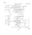
- FIG. 1 is a plan view showing a semiconductor device according to an embodiment of the present invention.
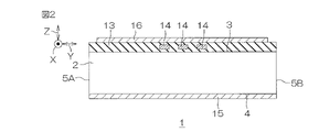
- FIG. 2 is a cross-sectional view taken along the line II-II shown in FIG.
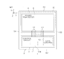
- FIG. 3 is a plan view showing the structure of the semiconductor chip shown in FIG.
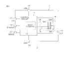
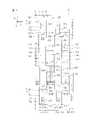
- FIG. 4 is a block circuit diagram showing an electrical structure of the semiconductor device shown in FIG.
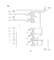
- FIG. 5 is an equivalent circuit diagram of the power transistor shown in FIG.
- FIG. 6 is a further equivalent circuit diagram of the power transistor shown in FIG.
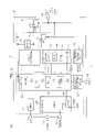
- FIG. 7 is a block circuit diagram showing a configuration example of the semiconductor device shown in FIG.
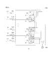
- FIG. 8A is a circuit diagram for explaining an operation example of the power transistor.
- FIG. 8B is a circuit diagram for explaining an operation example of the power transistor.
- FIG. 8A is a circuit diagram for explaining an operation example of the power transistor.
- FIG. 8B is a circuit diagram for explaining an operation example of the power transistor.
- FIG. 8A is a circuit diagram for explaining an operation example of
- FIG. 8C is a circuit diagram for explaining an operation example of the power transistor.
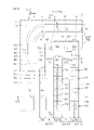
- FIG. 9 is an enlarged view of the region IX shown in FIG.
- FIG. 10 is an enlarged view of the region X shown in FIG.
- FIG. 11 is an enlarged view showing the area XI shown in FIG. 9 with a part omitted.
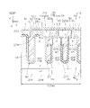
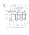
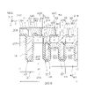
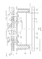
- FIG. 12 is a cross-sectional view taken along the line XII-XII shown in FIG.
- FIG. 13 is a cross-sectional view taken along the line XIII-XIII shown in FIG.
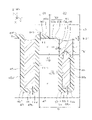
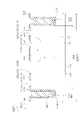
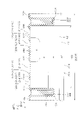
- FIG. 14A is an enlarged cross-sectional view of a main part of the structure shown in FIG. 14B is an enlarged cross-sectional view showing a main part of FIG. 14A.
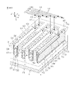
- FIG. 15 is a cross-sectional perspective view showing a main part of the first device region shown in FIG.
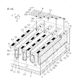
- FIG. 16A is a cross-sectional perspective view showing a control example of the power transistor.
- FIG. 16B is a cross-sectional perspective view showing a control example of the power transistor.
- FIG. 16C is a cross-sectional perspective view showing a control example of the power transistor.
- FIG. 17 is an enlarged view of the region XVII shown in FIG.
- FIG. 18 is a cross-sectional view taken along the line XVIII-XVIII shown in FIG.
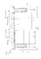
- FIG. 19 is an enlarged cross-sectional view of a main part of the structure shown in FIG.
- FIG. 20 is a cross-sectional view taken along the line XX-XX shown in FIG.
- FIG. 20 is a cross-sectional view taken along the line XX-XX shown in FIG.
- FIG. 21 is an enlarged cross-sectional view of a main part of the structure shown in FIG.
- FIG. 22A corresponds to the region shown in FIG. 12 and is a cross-sectional view for explaining an example of a method for manufacturing a semiconductor device.
- 22B is a cross-sectional view for explaining the process after FIG. 22A.
- 22C is a cross-sectional view for explaining the process after FIG. 22B.
- 22D is a cross-sectional view for explaining the process after FIG. 22C.
- 22E is a cross-sectional view for explaining the process after FIG. 22D.
- 22F is a cross-sectional view for explaining the process after FIG. 22E.
- FIG. 22G is a cross-sectional view for explaining the process after FIG. 22F.
- 22H is a cross-sectional view for explaining the process after FIG. 22G.
- 22I is a cross-sectional view for explaining the process after FIG. 22H.
- 22J is a cross-sectional view for explaining the process after FIG. 22I.
- 22K is a cross-sectional view for explaining the process after FIG. 22J.
- FIG. 22L is a cross-sectional view for explaining the process after FIG. 22K.
- 22M is a cross-sectional view for explaining the process after FIG. 22L.
- 22N is a cross-sectional view for explaining the process after FIG. 22M.
- FIG. 22O is a cross-sectional view for explaining the process after FIG. 22N.
- 22P is a cross-sectional view for explaining the process after FIG. 22O.
- 22Q is a cross-sectional view for explaining the process after FIG. 22P.
- 22R is a cross-sectional view for explaining the process after FIG. 22Q.
- 22S is a cross-sectional view for explaining the process after FIG. 22R.
- 22T is a cross-sectional view for explaining the process after FIG. 22S.
- 22U is a cross-sectional view for explaining the process after FIG. 22T.
- FIG. 23A corresponds to the region shown in FIG. 18 and is a cross-sectional view for explaining an example of a method for manufacturing a semiconductor device.
- FIG. 23B is a cross-sectional view for explaining the process after FIG. 23A.
- FIG. 23C is a cross-sectional view for explaining the process after FIG. 23B.
- FIG. 23D is a cross-sectional view for explaining the process after FIG. 23C.
- FIG. 23E is a cross-sectional view for explaining the process after FIG. 23D.
- FIG. 23F is a cross-sectional view for explaining the process after FIG. 23E.
- FIG. 23G is a cross-sectional view for explaining the process after FIG. 23F.
- FIG. 23H is a cross-sectional view for explaining the process after FIG. 23G.
- FIG. 23I is a cross-sectional view for explaining the process after FIG. 23H.
- FIG. 23J is a cross-sectional view for explaining the process after FIG. 23I.
- FIG. 23K is a cross-sectional view for explaining the process after FIG. 23J.
- FIG. 23L is a cross-sectional view for explaining the process after FIG. 23K.
- FIG. 23M is a cross-sectional view for explaining the process after FIG. 23L.
- FIG. 23N is a cross-sectional view for explaining the process after FIG. 23M.
- FIG. 23O is a cross-sectional view for explaining the process after FIG. 23N.
- FIG. 23P is a cross-sectional view for explaining the process after FIG. 23O.
- FIG. 23Q is a cross-sectional view for explaining the process after FIG. 23P.
- FIG. 23R is a cross-sectional view for explaining the process after FIG. 23Q.
- FIG. 23S is a cross-sectional view for explaining the process after FIG. 23R.
- FIG. 23T is a cross-sectional view for explaining the process after FIG. 23S.
- FIG. 23U is a cross-sectional view for explaining the process after FIG. 23T.
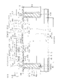
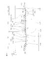
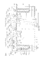
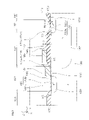
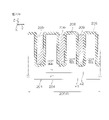
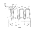
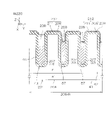
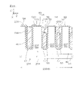
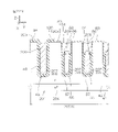
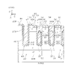
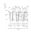
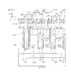
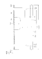
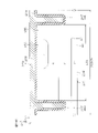
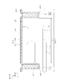
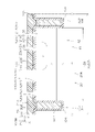
- FIG. 24 is a cross-sectional view showing a modified example of the first trench separation structure corresponding to FIG.
- FIG. 1 is a plan view showing a semiconductor device 1 according to an embodiment of the present invention.
- FIG. 2 is a cross-sectional view taken along the line II-II shown in FIG.
- FIG. 3 is a plan view showing the structure of the semiconductor chip 2 shown in FIG.
- FIG. 4 is a block circuit diagram showing an electrical structure of the semiconductor device 1 shown in FIG.
- FIG. 5 is an equivalent circuit diagram of the power transistor 8 shown in FIG.
- FIG. 6 is a further equivalent circuit diagram of the power transistor 8 shown in FIG.
- the semiconductor device 1 is composed of a switching device on the high side side
- the semiconductor device 1 can be used as a switching device on the low side side by adjusting the electrical connection form and function of various structures. Can also be provided.
- the semiconductor device 1 includes a semiconductor chip 2 formed in a rectangular parallelepiped shape in this embodiment.
- the semiconductor chip 2 is made of a Si (silicon) chip.
- the semiconductor chip 2 has a first main surface 3 on one side, a second main surface 4 on the other side, and first to fourth side surfaces 5A to 5D connecting the first main surface 3 and the second main surface 4. is doing.
- the first main surface 3 and the second main surface 4 are formed in a rectangular shape in a plan view (hereinafter, simply referred to as “plan view”) viewed from their normal direction Z.
- the first main surface 3 is a device surface on which a functional device is formed.
- the second main surface 4 is a mounting surface, and may be a grinding surface having a grinding mark.
- the first to fourth side surfaces 5A to 5D include a first side surface 5A, a second side surface 5B, a third side surface 5C, and a fourth side surface 5D.
- the first side surface 5A and the second side surface 5B extend in the first direction X along the first main surface 3 and face the second direction Y intersecting (specifically, orthogonal to) the first direction X.
- the third side surface 5C and the fourth side surface 5D extend in the second direction Y and face the first direction X.
- the semiconductor device 1 includes a first device region 6 partitioned on a first main surface 3.
- the first device area 6 is an output area in which an output signal to be output to the outside is generated.
- the first device region 6 is partitioned into a region on the third side surface 5C side in the first main surface 3.
- the arrangement and planar shape of the first device region 6 are arbitrary and are not limited to a specific form. However, from the viewpoint of obtaining good output characteristics, it is preferable that the first device region 6 occupies an area of one half or more of the first main surface 3.
- the semiconductor device 1 includes a second device region 7 partitioned in a region different from the first device region 6 on the first main surface 3.
- the second device area 7 is an input area in which an electric signal from the outside is input.
- the second device region 7 is partitioned into a region on the 4th side surface 5D side with respect to the first device region 6.
- the arrangement and planar shape of the second device region 7 are arbitrary and are not limited to a specific form.
- the second device area 7 preferably has a flat area equal to or smaller than the flat area of the first device area 6.
- the second device region 7 is preferably formed in an area ratio of 0.1 or more and 1 or less with respect to the first device region 6.
- the area ratio is the ratio of the flat area of the second device region 7 to the flat area of the first device region 6.
- the area ratio may be 0.1 or more and 0.25 or less, 0.25 or more and 0.5 or less, 0.5 or more and 0.75 or less, or 0.75 or more and 1 or less.
- the area ratio is preferably less than 1.
- the second device area 7 having a flat area exceeding the flat area of the first device area 6 may be adopted.
- the semiconductor device 1 includes an n-system (n ⁇ 2) power transistor 8 as an example of an insulated gate type gate split transistor formed in the first device region 6.
- the power transistor 8 may be referred to as a power MISFET (Metal Insulator Semiconductor Field Effect Transistor).
- the power transistor 8 includes one main drain DM, one main source SM, and n (n ⁇ 2) main gate GMs.
- the same or different n gate signals G are input to the n main gate GMs at arbitrary timings.
- the gate signal G includes an on signal that controls the power transistor 8 in the on state and an off signal that controls the power transistor 8 in the off state.
- the power transistor 8 outputs a single output current IOUT (output signal) from the main drain DM and the main source SM in response to the n gate signals G input to the n main gate GMs. That is, the power transistor 8 is composed of a multi-input single output type switching device.
- the output current IOUT is specifically a drain source current flowing between the main drain DM and the main source SM.
- the power transistor 8 specifically includes n (n ⁇ 2) system transistors 9 as individual control targets. More specifically, the power transistor 8 is composed of a parallel circuit of n system transistors 9 connected in parallel so that n gate signals G are individually input. In this embodiment, the n system transistors 9 are collectively formed in a single first device region 6. The n system transistors 9 are configured to be electrically controlled independently of each other in an on state and an off state. That is, the n-system power transistor 8 is configured so that the on-state system transistor 9 and the off-state system transistor 9 coexist at arbitrary timings.
- the n system transistors 9 include a system drain DS, a system source SS, and a system gate GS, respectively.
- the system drain DS of the n system transistors 9 is connected to the main drain DM, respectively.
- the system source SS of the n system transistors 9 is connected to the main source SM, respectively.
- the system gate GS of the n system transistors 9 is connected to the main gate GM in a one-to-one correspondence.
- the main drain DM of the power transistor 8, the main source SM, and the n main gate GMs are composed of the system drain DS of the n system transistors 9, the system source SS, and the n system gates GS, respectively.
- the n main gate GMs are substantially composed of n system gates GS.
- the n system transistors 9 generate an electric signal for each system in response to the gate signal G and output it to the main drain DM and the main source SM.
- the electric signal for each system is a drain source current flowing between the system drain DS and the system source SS of each system transistor 9.
- the electrical signal for each system is added between the main drain DM and the main source SM. This produces a single output current IOUT.
- the n system transistors 9 have gate threshold voltages substantially equal to each other.
- the numerical value to be measured here, the gate threshold voltage of one system transistor 9
- the numerical value to be compared here, the gate threshold voltage of the other system transistor 9.
- the case where the value to be measured is within the range of 0.9 times or more and 1.1 times or less of the value to be compared is also included.
- the n system transistors 9 may have substantially the same channel area as each other, or may have different channel areas from each other. That is, the n system transistors 9 may have on-resistance characteristics that are substantially equal to each other, or may have on-resistance characteristics that are different from each other.
- the n system transistors 9 include one or more unit transistors 10 systematized (grouped) as individual control targets, respectively. Specifically, each of the n system transistors 9 is composed of a parallel circuit of one or a plurality of unit transistors 10. Even when the system transistor 9 is composed of a single unit transistor 10, it is included in the "parallel circuit" referred to here.
- each system transistor 9 The number of unit transistors 10 included in each system transistor 9 is arbitrary, but it is preferable that at least one system transistor 9 out of n system transistors 9 includes a plurality of unit transistors 10.
- the n system transistors 9 may be composed of the same number of unit transistors 10 or may be composed of different numbers of unit transistors 10.
- Each unit transistor 10 includes a unit drain DU, a unit source SU, and a unit gate GU.
- the unit drain DU of one or more unit transistors 10 is electrically connected to the system drain DS.
- the unit source SU of one or more unit transistors 10 is electrically connected to the system source SS.
- the unit gate GU of one or more unit transistors 10 is electrically connected to the system gate GS.
- each system transistor 9 is each composed of a unit drain DU, a unit source SU, and a unit gate GU of one or more unit transistors 10.
- the plurality of unit transistors 10 may be of a trench gate type or a planar gate type. It is preferable that the plurality of unit transistors 10 have gate threshold voltages substantially equal to each other. Further, the plurality of unit transistors 10 may have substantially the same channel area as each other, or may have different channel areas from each other. That is, the plurality of unit transistors 10 may have on-resistance characteristics that are substantially equal to each other, or may have on-resistance characteristics that are different from each other.
- each system transistor 9 By adjusting the number of a plurality of unit transistors 10, the gate threshold voltage, the channel area, etc., the gate threshold voltage and the on-resistance characteristics (channel area) of each system transistor 9 can be precisely adjusted.
- the electrical characteristics of each system transistor 9 are adjusted according to the electrical specifications of the power transistor 8 to be achieved. Examples of the electrical specifications of the power transistor 8 include channel utilization, on-resistance Ron, switching waveform, and the like.
- the semiconductor device 1 includes a control IC 11 (Control Integrated Circuit) as an example of a control circuit formed in the second device region 7.
- the control IC 11 includes a plurality of types of functional circuits that realize various functions in response to an electric signal input from the outside.
- the plurality of types of functional circuits include a gate control circuit 12 that drives and controls the power transistor 8 in response to an electric signal from the outside.
- the gate control circuit 12 is configured to generate n gate signals G that individually control n system transistors 9.
- the control IC 11 forms a so-called IPD (Intelligent Power Device) together with the power transistor 8. IPD is also called IPM (Intelligent Power Module).
- the semiconductor device 1 includes an interlayer insulating layer 13 that covers the first main surface 3.
- the interlayer insulating layer 13 collectively covers the first device region 6 and the second device region 7.
- the interlayer insulating layer 13 is composed of a multilayer wiring structure having a laminated structure in which a plurality of insulating layers and a plurality of wiring layers are alternately laminated.
- Each insulating layer contains at least one of a SiO 2 film and a SiN film.
- Each wiring layer may include at least one of an Al layer, a Cu layer, an AlCu alloy layer, an AlSiCu alloy layer and an AlSi alloy layer.
- the semiconductor device 1 includes n gate wirings 14 as an example of control wirings formed on the first main surface 3 (anywhere above).
- the n gate wirings 14 are composed of n wiring layers formed in the interlayer insulating layer 13.
- the n gate wirings 14 are selectively routed in the interlayer insulating layer 13 and are electrically connected to the n main gate GMs of the power transistor 8 and the control IC 11 (gate control circuit 12), respectively.
- the n gate wirings 14 are electrically connected to the n main gates GM (n system gates GS) of the power transistor 8 in a one-to-one correspondence state in a state of being electrically independent from each other. Has been done. As a result, the n gate wirings 14 individually transmit the n gate signals G generated by the control IC 11 (gate control circuit 12) to the n main gate GMs of the power transistor 8.
- the n gate wirings 14 are electrically connected to the unit gate GU of one or a plurality of unit transistors 10 to be systematized as individual control targets from the aggregate composed of the plurality of unit transistors 10. ..
- the n gate wirings 14 may include one or more gate wirings 14 electrically connected to one unit transistor 10 to be systematized as an individual control target. Further, the n gate wirings 14 may include one or a plurality of gate wirings 14 for connecting a plurality of unit transistors 10 to be systematized as individual control targets in parallel.
- the semiconductor device 1 includes a plurality of (six in this form) terminal electrodes 15 to 20.
- a plurality of terminal electrodes 15 to 20 are shown by hatching.
- the number, arrangement, and planar shape of the plurality of terminal electrodes 15 to 20 are adjusted to any form according to the specifications of the power transistor 8 and the specifications of the control IC 11, and are not limited to the form shown in FIG.
- the plurality of terminal electrodes 15 to 20 include a drain terminal 15 (power supply terminal VBB), a source terminal 16 (output terminal OUT), an input terminal 17, a reference terminal 18, an enable terminal 19, and a sense terminal 20.
- the drain terminal 15 directly covers the second main surface 4 of the semiconductor chip 2 and is electrically connected to the second main surface 4.
- the drain terminal 15 is electrically connected to the main drain DM of the power transistor 8 and the control IC 11.
- the drain terminal 15 transmits the power supply voltage VB to the main drain DM of the power transistor 8 and various circuits of the control IC 11.
- the drain terminal 15 may include at least one of a Ti layer, a Ni layer, an Au layer, an Ag layer and an Al layer.
- the drain terminal 15 may have a laminated structure in which at least two of a Ti layer, a Ni layer, an Au layer, an Ag layer and an Al layer are laminated in any manner.
- the source terminal 16, the input terminal 17, the reference terminal 18, the enable terminal 19, and the sense terminal 20 are formed on the interlayer insulating layer 13.
- the source terminal 16 is formed on the first main surface 3 above the first device region 6.
- the source terminal 16 is electrically connected to the main source SM of the power transistor 8 and the control IC 11.
- the source terminal 16 transmits the output current IOUT generated by the power transistor 8 to the outside.
- the input terminal 17, the reference terminal 18, the enable terminal 19, and the sense terminal 20 are formed on the first main surface 3 above (specifically, above) a region outside the first device region 6 (specifically, the second device region 7). Has been done.
- the input terminal 17 transmits an input voltage for driving the control IC 11.
- the reference terminal 18 transmits a reference voltage (for example, ground voltage GND) to the power transistor 8 and the control IC 11.
- the enable terminal 19 transmits an electric signal for enabling or disabling a part or all of the functions of the control IC 11.
- the sense terminal 20 transmits an electric signal for detecting an abnormality in the control IC 11.
- the terminal electrodes 16 to 20 excluding the drain terminal 15 may include at least one of a pure Al layer, a pure Cu layer, an AlCu alloy layer, an AlSiCu alloy layer, and an AlSi alloy layer.
- a plating layer may be formed on the outer surface of the terminal electrodes 16 to 20, respectively.
- the plating layer may include at least one of a Ni layer, a Pd layer and an Au layer.
- FIG. 7 is a block circuit diagram showing a configuration example of the semiconductor device 1 shown in FIG. In the following, a case where the semiconductor device 1 is mounted on a vehicle will be described as an example.
- the semiconductor device 1 includes a drain terminal 15, a source terminal 16, an input terminal 17, a reference terminal 18, an enable terminal 19, a sense terminal 20, a power transistor 8, and a control IC 11.
- the drain terminal 15 is connected to the power supply.
- the power supply voltage VB may be 10 V or more and 20 V or less.
- the source terminal 16 is connected to the inductive load L.
- the inductive load L may be an inductance component of a coil, a solenoid, a harness, or the like.
- the input terminal 17 is externally connected to an MCU (MicroControllerUnit), a DC / DC converter or an LDO (LowDropOut).
- the input voltage may be 1 V or more and 10 V or less.
- the reference terminal 18 is grounded to the ground.
- the enable terminal 19 may be connected to the MCU. An electric signal for enabling or disabling a part or all of the functions of the control IC 11 is input to the enable terminal 19.
- the sense terminal 20 may be connected to a resistor.
- the main drain DM of the power transistor 8 is electrically connected to the drain terminal 15.
- the main source SM of the power transistor 8 is electrically connected to the control IC 11 (current detection circuit 26 described later) and the source terminal 16.
- the n main gate GMs of the power transistor 8 are electrically connected to the control IC 11 (specifically, the gate control circuit 12) via the n gate wiring 14.
- n gate wirings 14 are shown simplified by one line.
- the control IC 11 includes a gate control circuit 12, a sense transistor 21, an input circuit 22, a current / voltage control circuit 23, a protection circuit 24, an active clamp circuit 25, a current detection circuit 26, a power supply reverse connection protection circuit 27, and an abnormality detection circuit 28.
- the sense transistor 21 includes a drain, a source and a gate. The gate of the sense transistor 21 is electrically connected to the gate control circuit 12. The drain of the sense transistor 21 is electrically connected to the drain terminal 15. The source of the sense transistor 21 is electrically connected to the current detection circuit 26.
- the input circuit 22 is electrically connected to the input terminal 17 and the current / voltage control circuit 23.
- the input circuit 22 may include a Schmitt trigger circuit.
- the input circuit 22 shapes the waveform of the electric signal applied to the input terminal 17.
- the signal generated by the input circuit 22 is input to the current / voltage control circuit 23.
- the current / voltage control circuit 23 is electrically connected to the protection circuit 24, the gate control circuit 12, the power supply reverse connection protection circuit 27, and the abnormality detection circuit 28.
- the current / voltage control circuit 23 may include a logic circuit.
- the current / voltage control circuit 23 generates various voltages and currents in response to the electric signal from the input circuit 22 and the electric signal from the protection circuit 24.
- the current / voltage control circuit 23 includes a drive voltage generation circuit 29, a first constant voltage generation circuit 30, a second constant voltage generation circuit 31, and a reference voltage / current generation circuit 32.
- the drive voltage generation circuit 29 generates a drive voltage for driving the gate control circuit 12.
- the drive voltage may be set to a value obtained by subtracting a predetermined value from the power supply voltage VB.
- the drive voltage generation circuit 29 may generate a drive voltage of 5 V or more and 15 V or less obtained by subtracting 5 V from the power supply voltage VB.
- the drive voltage is input to the gate control circuit 12.
- the first constant voltage generation circuit 30 generates a first constant voltage for driving the protection circuit 24.
- the first constant voltage generation circuit 30 may include a Zener diode or a regulator circuit (here, a Zener diode).
- the first constant voltage may be 1 V or more and 5 V or less.
- the first constant voltage is input to the protection circuit 24 (specifically, the load open detection circuit 34 and the like described later).
- the second constant voltage generation circuit 31 generates a second constant voltage for driving the protection circuit 24.
- the second constant voltage generation circuit 31 may include a Zener diode and a regulator circuit (here, a regulator circuit).
- the second constant voltage may be 1 V or more and 5 V or less.
- the second constant voltage is input to the protection circuit 24 (specifically, the overheat protection circuit 35 and the low voltage malfunction suppression circuit 36 described later).
- the reference voltage / current generation circuit 32 generates reference voltage and reference current for various circuits.
- the reference voltage may be 1 V or more and 5 V or less.
- the reference current may be 1 mA or more and 1 A or less.
- the reference voltage and reference current are input to various circuits. If the various circuits include a comparator, the reference voltage and reference current may be input to the comparator.
- the protection circuit 24 is electrically connected to the current / voltage control circuit 23, the gate control circuit 12, the abnormality detection circuit 28, the source of the power transistor 8, and the source of the sense transistor 21.
- the protection circuit 24 includes an overcurrent protection circuit 33, a load open detection circuit 34, an overheat protection circuit 35, and a low voltage malfunction suppression circuit 36.
- the overcurrent protection circuit 33 is electrically connected to the source of the gate control circuit 12 and the sense transistor 21.
- the overcurrent protection circuit 33 protects the power transistor 8 from overcurrent by detecting the output current flowing through the power transistor 8 and limiting the output current to a certain value or less.
- the overcurrent protection circuit 33 may include a current monitor circuit.
- the signal generated by the overcurrent protection circuit 33 is input to the gate control circuit 12 (specifically, a drive signal output circuit described later).
- the load open detection circuit 34 is electrically connected to the current / voltage control circuit 23 and the main source SM of the power transistor 8.
- the load open detection circuit 34 detects the open state of the load.
- the signal generated by the load open detection circuit 34 is input to the current / voltage control circuit 23.
- the overheat protection circuit 35 is electrically connected to the current / voltage control circuit 23.
- the overheat protection circuit 35 monitors the temperature of the power transistor 8 and protects the power transistor 8 from an excessive temperature rise.
- the overheat protection circuit 35 forcibly turns off the power transistor 8 when the temperature of the power transistor 8 reaches a predetermined threshold value or when the temperature difference between the power transistor 8 and other circuits reaches a predetermined threshold value. Control to state.
- the superheat protection circuit 35 may include a temperature sensitive device such as a temperature sensitive diode or a thermistor.
- the signal generated by the overheat protection circuit 35 is input to the current / voltage control circuit 23.
- the low voltage malfunction suppression circuit 36 is electrically connected to the current / voltage control circuit 23.
- the low voltage malfunction suppression circuit 36 suppresses the malfunction of the power transistor 8 when the power supply voltage VB is less than a predetermined value.
- the signal generated by the low voltage malfunction suppression circuit 36 is input to the current / voltage control circuit 23.
- the gate control circuit 12 is electrically connected to the current / voltage control circuit 23, the protection circuit 24, the n main gate GMs of the power transistor 8, and the gate of the sense transistor 21.
- the gate control circuit 12 may include an oscillation circuit and a charge pump circuit.
- the gate control circuit 12 controls the on / off of the power transistor 8 in response to the electric signal from the current / voltage control circuit 23 and the electric signal from the protection circuit 24.
- the gate control circuit 12 generates n gate signals G to be output to the n gate wiring 14.
- the n gate signals G are input to the power transistor 8 via the n gate wiring 14.
- the gate control circuit 12 controls the on / off of the sense transistor 21.
- the gate control circuit 12 generates a gate signal to be output to the gate of the sense transistor 21 in response to the electric signal from the current / voltage control circuit 23 and the electric signal from the protection circuit 24.
- the on / off of the sense transistor 21 is controlled.
- the sense transistor 21 is preferably controlled at the same time as the power transistor 8.
- the active clamp circuit 25 is electrically connected to the drain terminal 15, the main gate GM of the power transistor 8, and the gate of the sense transistor 21.
- the active clamp circuit 25 protects the power transistor 8 from counter electromotive force.
- the active clamp circuit 25 may include a plurality of diodes.
- the active clamp circuit 25 may have a diode pair including a first diode row and a second diode row connected in reverse bias.
- the first diode row includes one or more diodes connected in series in the forward direction.
- the second diode train contains one or more diodes connected in series in the forward direction and is reverse biased to the first diode train.
- the one or more diodes constituting the first diode train may include at least one of a pn junction diode and a Zener diode.
- the one or more diodes constituting the second diode train may include at least one of a pn junction diode and a Zener diode.
- the current detection circuit 26 is electrically connected to the protection circuit 24, the abnormality detection circuit 28, the source of the power transistor 8, and the source of the sense transistor 21.
- the current detection circuit 26 detects the current flowing through the power transistor 8 and the sense transistor 21 and generates a current detection signal.
- the current detection signal is input to the abnormality detection circuit 28.
- the power supply reverse connection protection circuit 27 is electrically connected to the reference terminal 18 and the current / voltage control circuit 23.
- the power supply reverse connection protection circuit 27 protects the current / voltage control circuit 23, the power transistor 8 and the like from the reverse voltage when the power supply is reversely connected.
- the abnormality detection circuit 28 is electrically connected to the current / voltage control circuit 23, the protection circuit 24, and the current detection circuit 26.
- the abnormality detection circuit 28 monitors the voltage of the protection circuit 24.
- an abnormality voltage fluctuation, etc.
- the abnormality detection circuit 28 uses the voltage of the protection circuit 24. Generates an abnormality detection signal according to the above and outputs it to the outside.
- the abnormality detection circuit 28 includes a first multiplexer circuit 37 and a second multiplexer circuit 38.
- the first multiplexer circuit 37 includes two input units, one output unit, and one selective input unit.
- a protection circuit 24 and a current detection circuit 26 are connected to the input portion of the first multiplexer circuit 37, respectively.
- a second multiplexer circuit 38 is connected to the output unit of the first multiplexer circuit 37.
- a current / voltage control circuit 23 is connected to the selective input unit of the first multiplexer circuit 37.
- the first multiplexer circuit 37 generates an abnormality detection signal in response to an electric signal from the current / voltage control circuit 23, a voltage detection signal from the protection circuit 24, and a current detection signal from the current detection circuit 26.
- the abnormality detection signal generated by the first multiplexer circuit 37 is input to the second multiplexer circuit 38.
- the second multiplexer circuit 38 includes two input units and one output unit. An output unit of the first multiplexer circuit 37 and an enable terminal 19 are connected to the input unit of the second multiplexer circuit 38, respectively.
- a sense terminal 20 is connected to the output unit of the second multiplexer circuit 38.
- an on signal is input from the MCU to the enable terminal 19 and the resistor is connected to the sense terminal 20, an on signal is input from the MCU to the enable terminal 19, and an abnormality detection signal is taken out from the sense terminal 20.
- the abnormality detection signal is converted into a voltage signal by a resistor electrically connected to the sense terminal 20.
- the state abnormality of the semiconductor device 1 is detected based on this voltage signal.
- FIGS. 5 are circuit diagrams for explaining an operation example of the power transistor 8.
- a gate signal G that is, an on signal
- all the system transistors 9 are turned on.
- the power transistor 8 is turned on with all current paths open. Therefore, the channel utilization rate of the power transistor 8 is relatively increased, and the on-resistance Ron is relatively decreased.
- a gate signal G (that is, an on signal) exceeding the gate threshold voltage is input to the x (1 ⁇ x ⁇ n) gate wirings 14, and the gates 14 are gated to the (nx) gate wirings 14.
- a gate signal G that is, an off signal
- the x system transistors 9 are turned on and the (nx) system transistors 9 are turned off.
- the power transistor 8 is turned on with a part of the current path closed. Therefore, the channel utilization rate of the power transistor 8 is relatively reduced, and the on-resistance Ron is relatively increased.
- FIG. 9 is an enlarged view of the region IX shown in FIG.
- FIG. 10 is an enlarged view of the region X shown in FIG.
- FIG. 11 is an enlarged view showing the area XI shown in FIG. 9 with a part omitted.
- FIG. 12 is a cross-sectional view taken along the line XII-XII shown in FIG.
- FIG. 13 is a cross-sectional view taken along the line XIII-XIII shown in FIG.
- FIG. 14A is an enlarged cross-sectional view of a main part of the structure shown in FIG. 14B is an enlarged cross-sectional view showing a main part of FIG. 14A.
- FIG. 15 is a cross-sectional perspective view showing a main part of the first device region 6 shown in FIG. In FIG. 14B, hatching is omitted for convenience. In FIG. 15, for convenience, the structure on the first main surface 3 is omitted, and the gate wiring 14 and the like are simplified.
- the semiconductor device 1 is a first n-type (first conductive type) formed on the surface layer portion of the second main surface 4 of the semiconductor chip 2.
- the semiconductor region 41 is included.
- the first semiconductor region 41 forms the main drain DM of the power transistor 8.
- the first semiconductor region 41 may be referred to as a drain region.
- the first semiconductor region 41 is formed over the entire surface layer portion of the second main surface 4, and is exposed from the second main surface 4 and the first to fourth side surfaces 5A to 5D.
- the concentration of n-type impurities in the first semiconductor region 41 may be 1 ⁇ 10 18 cm -3 or more and 1 ⁇ 10 21 cm -3 or less.
- the first semiconductor region 41 is formed of a semiconductor substrate (Si substrate).
- the thickness of the first semiconductor region 41 may be 10 ⁇ m or more and 450 ⁇ m or less.
- the thickness of the first semiconductor region 41 may be 10 ⁇ m or more and 50 ⁇ m or less, 50 ⁇ m or more and 150 ⁇ m or less, 150 ⁇ m or more and 250 ⁇ m or less, 250 ⁇ m or more and 350 ⁇ m or less, and 350 ⁇ m or more and 450 ⁇ m or less.
- the thickness of the first semiconductor region 41 is preferably 50 ⁇ m or more and 150 ⁇ m or less.
- the semiconductor device 1 includes an n-type second semiconductor region 42 formed on the surface layer portion of the first main surface 3 of the semiconductor chip 2.
- the second semiconductor region 42 forms the main drain DM of the power transistor 8 together with the first semiconductor region 41.
- the second semiconductor region 42 may be referred to as a drift region or a drain drift region.
- the second semiconductor region 42 is formed over the entire surface layer portion of the first main surface 3 so as to be electrically connected to the first semiconductor region 41, and the first main surface 3 and the first to fourth side surfaces 5A to 5D. It is exposed from.
- the second semiconductor region 42 has an n-type impurity concentration lower than the n-type impurity concentration of the first semiconductor region 41.
- the concentration of n-type impurities in the second semiconductor region 42 may be 1 ⁇ 10 15 cm -3 or more and 1 ⁇ 10 18 cm -3 or less.
- the second semiconductor region 42 is formed by an epitaxial layer (Si epitaxial layer) in this form.
- the second semiconductor region 42 has a thickness less than the thickness of the first semiconductor region 41.
- the thickness of the second semiconductor region 42 may be 5 ⁇ m or more and 20 ⁇ m or less.
- the thickness of the second semiconductor region 42 may be 5 ⁇ m or more and 10 ⁇ m or less, 10 ⁇ m or more and 15 ⁇ m or less, or 15 ⁇ m or more and 20 ⁇ m or less.
- the thickness of the second semiconductor region 42 is preferably 5 ⁇ m or more and 15 ⁇ m or less.
- the semiconductor device 1 includes a first trench separation structure 43 (first trench separation structure) as an example of a region separation structure for partitioning the first device region 6 on the first main surface 3.
- the first trench separation structure 43 may be referred to as a DTI (deep trench isolation) structure or an STI (shallow trench isolation) structure.
- the first trench separation structure 43 is formed in an annular shape surrounding a part of the first main surface 3 in a plan view, and partitions the first device region 6 having a predetermined shape.
- the first trench separation structure 43 is formed in a square ring having four sides parallel to the first to fourth side surfaces 5A to 5D in a plan view, and partitions the first device region 6 having a rectangular shape. ..
- the planar shape of the first trench separation structure 43 is arbitrary, and may be formed in a polygonal annular shape.
- the first device region 6 may be partitioned into a polygonal shape according to the planar shape of the first trench separation structure 43.
- the first trench separation structure 43 has a separation width WI.
- the separation width WI is a width in a direction orthogonal to the direction in which the first trench separation structure 43 extends.
- the separation width WI may be 0.5 ⁇ m or more and 2.5 ⁇ m or less.
- the separation width WI may be 0.5 ⁇ m or more and 1 ⁇ m or less, 1 ⁇ m or more and 1.5 ⁇ m or less, 1.5 ⁇ m or more and 2 ⁇ m or less, or 2 ⁇ m or more and 2.5 ⁇ m or less.
- the separation width WI is preferably 1.2 ⁇ m or more and 2 ⁇ m or less.
- the first trench separation structure 43 has a separation depth DI.
- the separation depth DI may be 1 ⁇ m or more and 10 ⁇ m or less.
- the separation depth DI may be 1 ⁇ m or more and 2.5 ⁇ m or less, 2.5 ⁇ m or more and 5 ⁇ m or less, 5 ⁇ m or more and 7.5 ⁇ m or less, or 7.5 ⁇ m or more and 10 ⁇ m or less.
- the separation depth DI is preferably 2 ⁇ m or more and 6 ⁇ m or less.
- the aspect ratio DI / WI of the first trench separation structure 43 may be more than 1 and 5 or less.
- the aspect ratio DI / WI is the ratio of the separation depth DI to the separation width WI.
- the aspect ratio DI / WI is preferably 2 or more.
- the bottom wall of the first trench separation structure 43 is preferably formed with an interval of 1 ⁇ m or more and 10 ⁇ m or less with respect to the bottom of the second semiconductor region 42. It is particularly preferable that the bottom wall of the first trench separation structure 43 is formed at intervals of 1 ⁇ m or more and 5 ⁇ m or less with respect to the bottom of the second semiconductor region 42.
- the first trench separation structure 43 has a corner portion that connects a portion extending in the first direction X and a portion extending in the second direction Y in an arc shape.
- the four corners of the first trench separation structure 43 are formed in an arc shape. That is, the first device region 6 is divided into a quadrangular shape having four corners extending in an arc shape. It is preferable that the corner portion of the first trench separation structure 43 has a constant separation width WI along the arc direction.
- the first trench separation structure 43 has a single electrode structure including a separation trench 44, a separation insulating film 45 (separation insulator), and a separation electrode 46.
- the separation trench 44 is dug down from the first main surface 3 to the second main surface 4.
- the separation trench 44 is formed at intervals from the bottom of the second semiconductor region 42 to the first main surface 3 side.
- the separation trench 44 includes a side wall and a bottom wall.
- the angle formed by the side wall of the separation trench 44 with the first main surface 3 in the semiconductor chip 2 may be 90 ° or more and 92 ° or less.
- the separation trench 44 may be formed in a tapered shape in which the opening width narrows from the opening toward the bottom wall.
- the bottom wall corner of the separation trench 44 is preferably formed in a curved shape.
- the entire bottom wall of the separation trench 44 may be formed in a curved shape toward the second main surface 4.
- the separation insulating film 45 is formed on the wall surface of the separation trench 44. Specifically, the separation insulating film 45 is formed in a film shape over the entire wall surface of the separation trench 44, and partitions a U-shaped recess space in the separation trench 44.
- the separation insulating film 45 includes a silicon oxide film in this form. Specifically, the separation insulating film 45 includes a silicon oxide film made of an oxide of the semiconductor chip 2.
- the separation insulating film 45 has a separation thickness TI.
- the separation thickness TI is the thickness of the separation insulating film 45 along the normal direction of the wall surface of the separation trench 44.
- the separation thickness TI may be 0.1 ⁇ m or more and 1 ⁇ m or less.
- the separation thickness TI may be 0.1 ⁇ m or more and 0.25 ⁇ m or less, 0.25 ⁇ m or more and 0.5 ⁇ m or less, 0.5 ⁇ m or more and 0.75 ⁇ m or less, or 0.75 ⁇ m or more and 1 ⁇ m or less.
- the separation thickness TI is preferably 0.15 ⁇ m or more and 0.65 ⁇ m or less.
- the separation insulating film 45 includes a first portion 45a and a second portion 45b.
- the first portion 45a is a portion that covers the side wall of the separation trench 44.
- the second portion 45b is a portion that covers the bottom wall of the separation trench 44.
- the first portion 45a has a first separation thickness TI1.
- the first separation thickness TI1 is the thickness of the first portion 45a along the normal direction of the side wall of the separation trench 44.
- the separation thickness TI of the separation insulating film 45 is defined by the first separation thickness TI1.
- the second portion 45b has a second separation thickness TI2 (TI1 ⁇ TI2) different from the first separation thickness TI1.
- the second separation thickness TI2 is the thickness of the second portion 45b along the normal direction of the bottom wall of the separation trench 44.
- the second separation thickness TI2 is preferably less than the first separation thickness TI1 (TI2 ⁇ TI1).
- the second separation thickness TI2 may be 0.6 times or more and less than 1 times the first separation thickness TI1.
- the second separation thickness TI2 is preferably 0.7 times or more and 0.9 times or less the first separation thickness TI1.
- the separation electrode 46 is embedded as an integral part in the separation trench 44 with the separation insulating film 45 interposed therebetween.
- the separation electrode 46 in this form, comprises conductive polysilicon.
- a source voltage (for example, a ground voltage) as a reference voltage may be applied to the separation electrode 46.
- the semiconductor device 1 includes a p-type (second conductive type) body region 47 formed on the surface layer portion of the first main surface 3 in the first device region 6.
- the concentration of p-type impurities in the body region 47 may be 1 ⁇ 10 16 cm -3 or more and 1 ⁇ 10 18 cm -3 or less.
- the body region 47 is formed in the entire surface layer portion of the first main surface 3 in the first device region 6 and is in contact with the first trench separation structure 43.
- the body region 47 is formed in a region on the first main surface 3 side with respect to the bottom wall of the first trench separation structure 43. Specifically, the body region 47 is formed in a region on the first main surface 3 side with respect to the intermediate portion of the first trench separation structure 43.
- the semiconductor device 1 includes a body space 48 formed along the inner peripheral wall of the first trench separation structure 43 in the first device region 6.
- the body space 48 comprises a part of the body area 47.
- the body space 48 is formed in an annular shape along the inner peripheral wall of the first trench separation structure 43 in a plan view, and surrounds the inside of the first device region 6.
- the body space 48 has a space width WSP.
- the space width WSP may be greater than or equal to the separation width WI (WI ⁇ WSP) or less than or equal to the separation width WI (WSP ⁇ WI).
- the body space 48 preferably has a constant space width WSP along the inner peripheral wall of the first trench separation structure 43.
- the space width WSP may be 1 ⁇ m or more and 2.5 ⁇ m or less.
- the space width WSP may be 1 ⁇ m or more and 1.5 ⁇ m or less, 1.5 ⁇ m or more and 2 ⁇ m or less, or 2 ⁇ m or more and 2.5 ⁇ m or less.
- the space width WSP is preferably 1.2 ⁇ m or more and 2 ⁇ m or less.
- the semiconductor device 1 includes a power transistor 8 formed on the first main surface 3 in the first device region 6.
- the power transistor 8 is formed on the first main surface 3 with a space width WSP from the first trench separation structure 43. As a result, the power transistor 8 faces the first trench separation structure 43 with the body space 48 interposed therebetween.
- the power transistor 8 includes a plurality of unit transistors 10 collectively formed on the first main surface 3 of the first device region 6.
- FIG. 9 shows an example in which 16 unit transistors 10 are formed, but the number of unit transistors 10 is arbitrary.
- the plurality of unit transistors 10 are each formed in a band shape (rectangular shape) extending in the first direction X in a plan view, and are arranged side by side in a row in the second direction Y. As a result, the plurality of unit transistors 10 are formed in a striped shape extending in the first direction X in a plan view.
- each unit cell 50 includes one trench gate structure 51 and a channel cell 52 controlled by the trench gate structure 51.
- the channel cell 52 is a region in which the opening / closing of the current path is controlled by the trench gate structure 51.
- the unit cell 50 includes a pair of channel cells 52 formed on both sides of one trench gate structure 51.
- the cell width of the unit cell 50 may be 1 ⁇ m or more and 5 ⁇ m or less.
- the cell width is the width in the direction orthogonal to the direction in which the unit cell 50 extends (that is, the second direction Y).
- the length of the unit cell 50 in the first direction X is arbitrary and is adjusted by the length of the trench gate structure 51.
- the structure of one unit transistor 10 (unit cell 50) will be described, and then the arrangement of a plurality of unit transistors 10 (unit cell 50) will be described.
- the trench gate structure 51 is formed in a band shape (rectangular shape) extending in the first direction X in a plan view.
- the trench gate structure 51 has a first end portion 51A on one side and a second end portion 51B on the other side with respect to the first direction X (longitudinal direction).
- the trench gate structure 51 has a first width W1.
- the first width W1 is the width of the trench gate structure 51 in the lateral direction (second direction Y).
- the first width W1 may be substantially equal to the separation width WI of the first trench separation structure 43 (W1 ⁇ WI).
- the first width W1 is preferably less than the separation width WI (W1 ⁇ WI).
- the first width W1 is preferably less than the space width WSP (W1 ⁇ WSP).
- the first width W1 may be 0.5 ⁇ m or more and 2 ⁇ m or less.
- the first width W1 may be 0.5 ⁇ m or more and 1 ⁇ m or less, 1 ⁇ m or more and 1.5 ⁇ m or less, or 1.5 ⁇ m or more and 2 ⁇ m or less.
- the first width W1 is preferably 0.5 ⁇ m or more and 1.5 ⁇ m or less.
- the trench gate structure 51 has a first depth D1.
- the first depth D1 is substantially equal to the separation depth DI of the first trench separation structure 43 (D1 ⁇ DI).
- the first depth D1 is preferably less than the separation depth DI (D1 ⁇ DI).
- the first depth D1 may be 1 ⁇ m or more and 10 ⁇ m or less.
- the first depth D1 may be 1 ⁇ m or more and 2.5 ⁇ m or less, 2.5 ⁇ m or more and 5 ⁇ m or less, 5 ⁇ m or more and 7.5 ⁇ m or less, or 7.5 ⁇ m or more and 10 ⁇ m or less.
- the first depth D1 is preferably 2 ⁇ m or more and 6 ⁇ m or less.
- the aspect ratio D1 / W1 of the trench gate structure 51 may be more than 1 and 5 or less.
- the aspect ratio D1 / W1 is the ratio of the first depth D1 to the first width W1. It is particularly preferable that the aspect ratio D1 / W1 is 2 or more.
- the bottom wall of the trench gate structure 51 is preferably formed at a distance of 1 ⁇ m or more and 10 ⁇ m or less with respect to the bottom portion of the second semiconductor region 42. It is particularly preferable that the bottom wall of the trench gate structure 51 is formed at intervals of 1 ⁇ m or more and 5 ⁇ m or less with respect to the bottom portion of the second semiconductor region 42.
- the trench gate structure 51 has a multi-electrode structure including a gate trench 53, an upper insulating film 54, a lower insulating film 55, an upper electrode 56, a lower electrode 57, and an intermediate insulating film 58.
- the upper insulating film 54, the lower insulating film 55, and the intermediate insulating film 58 constitute the first insulating body.
- the upper electrode 56 and the lower electrode 57 are embedded in the gate trench 53 so as to be vertically insulated and separated by the first insulator.
- the gate trench 53 is dug down from the first main surface 3 to the second main surface 4.
- the gate trench 53 penetrates the body region 47 and is formed at intervals from the bottom of the second semiconductor region 42 to the first main surface 3 side.
- the gate trench 53 includes a side wall and a bottom wall.
- the angle formed by the side wall of the gate trench 53 with the first main surface 3 in the semiconductor chip 2 may be 90 ° or more and 92 ° or less.
- the gate trench 53 may be formed in a tapered shape in which the opening width narrows from the opening toward the bottom wall.
- the bottom wall corner of the gate trench 53 is preferably formed in a curved shape.
- the entire bottom wall of the gate trench 53 may be formed in a curved shape toward the second main surface 4.
- the upper insulating film 54 covers the upper wall surface of the gate trench 53. Specifically, the upper insulating film 54 covers the upper wall surface located in the region on the opening side of the gate trench 53 with respect to the bottom portion of the body region 47. The lower portion of the upper insulating film 54 crosses the boundary between the second semiconductor region 42 and the body region 47.
- the upper insulating film 54 has a portion that covers the body region 47 and a portion that covers the second semiconductor region 42.
- the covering area of the upper insulating film 54 with respect to the body region 47 is larger than the covering area of the upper insulating film 54 with respect to the second semiconductor region 42.
- the upper insulating film 54 contains silicon oxide in this form.
- the upper insulating film 54 includes a silicon oxide film made of an oxide of the semiconductor chip 2.
- the upper insulating film 54 is formed as a gate insulating film.
- the upper insulating film 54 has a first thickness T1 (T1 ⁇ TI) that is less than the separation thickness TI of the separation insulating film 45.
- the first thickness T1 is the thickness of the upper insulating film 54 along the normal direction of the wall surface of the gate trench 53.
- the first thickness T1 may be 0.01 ⁇ m or more and 0.05 ⁇ m or less.
- the first thickness T1 may be 0.01 ⁇ m or more and 0.02 ⁇ m or less, 0.02 ⁇ m or more and 0.03 ⁇ m or less, 0.03 ⁇ m or more and 0.04 ⁇ m or less, or 0.04 ⁇ m or more and 0.05 ⁇ m or less.
- the first thickness T1 is preferably 0.02 ⁇ m or more and 0.04 ⁇ m or less.
- the lower insulating film 55 covers the lower wall surface of the gate trench 53. Specifically, the lower insulating film 55 covers the lower wall surface located in the region on the bottom wall side of the gate trench 53 with respect to the bottom portion of the body region 47. The lower insulating film 55 partitions a U-shaped recess space in the region on the bottom wall side of the gate trench 53. The lower insulating film 55 is in contact with the second semiconductor region 42. The lower insulating film 55 contains silicon oxide in this form. Specifically, the lower insulating film 55 includes a silicon oxide film made of an oxide of the semiconductor chip 2. The lower insulating film 55 is formed as a field insulating film.
- the lower insulating film 55 has a second thickness T2 (T1 ⁇ T2) that exceeds the first thickness T1 of the upper insulating film 54.
- the second thickness T2 may be substantially equal to the separation thickness TI of the separation insulating film 45 (T2 ⁇ TI).
- the second thickness T2 is the thickness of the lower insulating film 55 along the normal direction of the wall surface of the gate trench 53.
- the second thickness T2 may be 0.1 ⁇ m or more and 1 ⁇ m or less.
- the second thickness T2 may be 0.1 ⁇ m or more and 0.25 ⁇ m or less, 0.25 ⁇ m or more and 0.5 ⁇ m or less, 0.5 ⁇ m or more and 0.75 ⁇ m or less, or 0.75 ⁇ m or more and 1 ⁇ m or less.
- the second thickness T2 is preferably 0.15 ⁇ m or more and 0.65 ⁇ m or less.
- the lower insulating film 55 includes a first portion 55a and a second portion 55b.
- the first portion 55a is a portion that covers the side wall of the gate trench 53.
- the second portion 55b is a portion that covers the bottom wall of the gate trench 53.
- the first portion 55a has a first lower thickness T21.
- the first lower thickness T21 is the thickness of the first portion 55a along the normal direction of the side wall of the gate trench 53.
- the second thickness T2 of the lower insulating film 55 is defined by the first lower thickness T21.
- the second portion 45b has a second lower thickness T22 (T21 ⁇ T22) different from the first lower thickness T21.
- the second lower thickness T22 is the thickness of the second portion 45b along the normal direction of the bottom wall of the gate trench 53.
- the second lower thickness T22 is preferably less than the first lower thickness T21 (T22 ⁇ T21).
- the second lower thickness T22 may be 0.6 times or more and less than 1 times the first lower thickness T21.
- the second lower thickness T22 is preferably 0.7 times or more and 0.9 times or less the first lower thickness T21.
- the second lower thickness T22 may be substantially equal to the second separation thickness TI2 of the separation insulating film 45 (T22 ⁇ TI2).
- the upper electrode 56 is embedded in the upper side (opening side) in the gate trench 53 with the upper insulating film 54 interposed therebetween.
- the upper electrode 56 is formed in a band shape (rectangular shape) extending in the first direction X in a plan view.
- the upper electrode 56 faces the body region 47 and the second semiconductor region 42 with the upper insulating film 54 interposed therebetween.
- the area of the upper electrode 56 facing the body region 47 is larger than the area of the upper electrode 56 facing the second semiconductor region 42.
- the upper electrode 56 in this form, comprises conductive polysilicon.
- the upper electrode 56 is formed as a gate electrode. A gate signal G is applied to the upper electrode 56.
- the lower electrode 57 is embedded in the lower side (bottom wall side) in the gate trench 53 with the lower insulating film 55 interposed therebetween.
- the lower electrode 57 faces the second semiconductor region 42 with the lower insulating film 55 interposed therebetween.
- the lower electrode 57 has an upper end portion protruding from the lower insulating film 55 toward the first main surface 3 side.
- the upper end of the lower electrode 57 extends toward the upper electrode 56 so as to occlude with the bottom of the upper electrode 56.
- the upper end portion of the lower electrode 57 faces the upper insulating film 54 with the bottom portion of the upper electrode 56 interposed therebetween in the second direction Y.
- the lower electrode 57 contains conductive polysilicon in this form.
- the lower electrode 57 is formed as a gate electrode in this form. Therefore, the gate signal G is applied to the lower electrode 57 at the same time as the upper electrode 56.
- the upper electrode 56 and the lower electrode 57 arranged in the common gate trench 53 are controlled at the same time. As a result, the voltage drop between the upper electrode 56 and the lower electrode 57 can be suppressed, so that the electric field concentration between the upper electrode 56 and the lower electrode 57 can be suppressed. Further, the on-resistance Ron of the semiconductor chip 2 (particularly the second semiconductor region 42) can be reduced. This structure is particularly effective when the semiconductor device 1 is provided as an in-vehicle device.
- the intermediate insulating film 58 is interposed between the upper electrode 56 and the lower electrode 57, and electrically insulates the upper electrode 56 and the lower electrode 57. Specifically, the intermediate insulating film 58 covers the lower electrode 57 (upper end portion) exposed from the lower insulating film 55 in the region between the upper electrode 56 and the lower electrode 57. The intermediate insulating film 58 is connected to the upper insulating film 54 and the lower insulating film 55.
- the intermediate insulating film 58 contains silicon oxide in this form. Specifically, the intermediate insulating film 58 includes a silicon oxide film made of an oxide of the lower electrode 57.
- the intermediate insulating film 58 has an intermediate thickness TM (TM ⁇ T2) that is less than the second thickness T2 of the lower insulating film 55 in the normal direction Z.
- the intermediate thickness TM may be 0.01 ⁇ m or more and 0.05 ⁇ m or less.
- the intermediate thickness TM may be 0.01 ⁇ m or more and 0.02 ⁇ m or less, 0.02 ⁇ m or more and 0.03 ⁇ m or less, 0.03 ⁇ m or more and 0.04 ⁇ m or less, or 0.04 ⁇ m or more and 0.05 ⁇ m or less.
- the intermediate thickness TM is preferably 0.02 ⁇ m or more and 0.04 ⁇ m or less.
- the pair of channel cells 52 are formed in a band shape extending in the first direction X on both sides of the trench gate structure 51.
- Each of the pair of channel cells 52 has a channel width WC.
- the channel width WC may be 0.1 ⁇ m or more and 1 ⁇ m or less.
- the pair of channel cells 52 each include an n-type source region 60 formed on the surface layer portion of the body region 47.
- the number of source regions 60 included in the pair of channel cells 52 is arbitrary.
- the pair of channel cells 52 in this embodiment, each include a plurality of source regions 60.
- One or more source regions 60 included in the unit cell 50 form a unit source SU (a part of the main source SM of the power transistor 8) of the unit transistor 10.
- the concentration of n-type impurities in the source region 60 exceeds the concentration of n-type impurities in the second semiconductor region 42.
- the concentration of n-type impurities in the source region 60 may be 1 ⁇ 10 18 cm -3 or more and 1 ⁇ 10 21 cm -3 or less.
- the plurality of source regions 60 are formed in each channel cell 52 at intervals in the first direction X.
- the bottom of the plurality of source regions 60 is located in the region on the first main surface 3 side with respect to the bottom of the body region 47.
- the pair of channel cells 52 each include a p-shaped contact region 61 formed in a region different from the source region 60 in the surface layer portion of the body region 47.
- the number of contact regions 61 included in the pair of channel cells 52 is arbitrary.
- the pair of channel cells 52 in this embodiment, each include a plurality of contact areas 61.
- the p-type impurity concentration in the contact region 61 exceeds the p-type impurity concentration in the body region 47.
- the concentration of p-type impurities in the contact region 61 may be 1 ⁇ 10 18 cm -3 or more and 1 ⁇ 10 21 cm -3 or less.
- the plurality of contact regions 61 are formed in each channel cell 52 at intervals in the first direction X. Specifically, the plurality of contact regions 61 are formed alternately with the plurality of source regions 60 in the first direction X in a manner of sandwiching one source region 60. The bottom of the plurality of contact regions 61 is located in the region on the first main surface 3 side with respect to the bottom of the body region 47.
- the pair of channel cells 52 includes a plurality of channel regions 62 defined between the plurality of source regions 60 and the second semiconductor region 42 in the body region 47.
- the on / off of the plurality of channel regions 62 is simultaneously controlled by the trench gate structure 51. Therefore, the plurality of channel regions 62 form one channel of the unit transistor 10.
- the plurality of unit cells 50 are formed so that a plurality of trench gate structures 51 are arranged side by side in a row with a first interval I1 in the second direction Y. That is, the plurality of trench gate structures 51 are each formed in a strip shape extending in the first direction X in the first device region 6 in a plan view, and are formed with a first interval I1 in the second direction Y. That is, the plurality of unit cells 50 (plural trench gate structures 51) are formed in a striped shape extending in the first direction X in a plan view.
- plateau-shaped mesa portions 63 extending in the first direction X are respectively partitioned. That is, the plurality of trench gate structures 51 are formed alternately with the plurality of mesa portions 63 in the second direction Y in a manner of sandwiching one mesa portion 63.
- the plurality of unit cells 50 are formed so that the channel cells 52 are integrated with each other in the mesa portion 63 located between a pair of adjacent unit cells 50.
- a plurality of source regions 60 and a plurality of contact regions 61 are alternately formed along the first direction X on the surface layer portion of the body region 47.
- the plurality of unit cells 50 are each formed by a region between the central portions of a pair of adjacent mesas portions 63 in this form.
- each unit cell 50 functions as one unit transistor 10.
- the trench gate structure 51 of the two unit cells 50 arranged on both sides is formed from the first trench separation structure 43 with a space width WSP in the first direction X, respectively.
- the two unit cells 50 arranged on both sides do not include the source region 60 in the channel cell 52 on the first trench separation structure 43 side in this embodiment.
- the main current path can be limited to the mesa portion 63, and at the same time, the leakage current between the trench gate structure 51 and the first trench separation structure 43 can be suppressed.
- the two unit cells 50 arranged on both sides include only the contact region 61 (hereinafter referred to as "outermost contact region 61") in the channel cell 52 on the first trench separation structure 43 side.
- the outermost contact region 61 is preferably formed at a distance from the first trench separation structure 43 to the trench gate structure 51 side.
- the outermost contact area 61 is connected to the side wall of the corresponding trench gate structure 51.
- the outermost contact region 61 may be formed in a strip extending along the side wall of the corresponding trench gate structure 51.
- the first interval I1 corresponds to a value obtained by doubling the channel width WC in this embodiment.
- the first interval I1 is preferably set to a value at which the depletion layer extending from the plurality of trench gate structures 51 is integrated below the bottom wall of the plurality of trench gate structures 51.
- the first interval I1 may be 0.25 times or more the first width W1 and 1.5 times or less the first width W1.
- the first interval I1 is preferably the first width W1 or less (I1 ⁇ W1).
- the first interval I1 is preferably less than the space width WSP (I1 ⁇ WSP).
- the first interval I1 may be 0.5 ⁇ m or more and 2 ⁇ m or less.
- the first interval I1 may be 0.5 ⁇ m or more and 1 ⁇ m or less, 1 ⁇ m or more and 1.5 ⁇ m or less, or 1.5 ⁇ m or more and 2 ⁇ m or less.
- the first interval I1 is preferably 0.4 ⁇ m or more and 1.6 ⁇ m or less.
- the semiconductor device 1 includes a plurality of (32 in this embodiment) trench contact structures 71 formed on the first main surface 3 in the first device region 6.
- the plurality of trench contact structures 71 are also components of the power transistor 8.
- the plurality of trench contact structures 71 include a plurality of (16 in this form) first trench contact structure 71A and a plurality of (16 in this form) second trench contact structures 71B.
- the plurality of first trench contact structures 71A are formed in the regions between the first end portion 51A and the first trench separation structure 43 of the plurality of trench gate structures 51, respectively.
- the plurality of first trench contact structures 71A are connected to the first end portions 51A of the plurality of trench gate structures 51, respectively, and are formed in a strip shape (rectangular shape) extending in the first direction X.
- the plurality of first trench contact structures 71A are formed at intervals of the space width WSP from the first trench separation structure 43 with respect to the first direction X.
- the length of the plurality of first trench contact structures 71A in the first direction X is arbitrary.
- the plurality of second trench contact structures 71B are formed in the regions between the second end portion 51B and the first trench separation structure 43 of the plurality of trench gate structures 51, respectively.
- the plurality of second trench contact structures 71B are connected to the second end portions 51B of the plurality of trench gate structures 51, respectively, and are formed in a strip shape (rectangular shape) extending in the first direction X.
- the plurality of second trench contact structures 71B are formed at intervals of the space width WSP from the first trench separation structure 43 with respect to the first direction X.
- the length of the plurality of second trench contact structures 71B in the first direction X is arbitrary.
- the plurality of trench contact structures 71 have a second width W2 and a second depth D2, respectively.
- the second width W2 is the width in the direction (second direction Y) orthogonal to the direction in which the trench contact structure 71 extends (first direction X).
- the second width W2 is substantially equal to the first width W1 of the trench gate structure 51 (W2 ⁇ W1).
- the second depth D2 is substantially equal to the first depth D1 of the trench gate structure 51 in this embodiment (D2 ⁇ D1). Therefore, the aspect ratio D2 / W2 of the plurality of trench contact structures 71 is substantially equal to the aspect ratio D1 / W1 (D2 / W2 ⁇ D1 / W1) of the trench gate structure 51.
- the plurality of trench contact structures 71 have a single electrode structure including a contact trench 72, a contact insulating film 73 (second insulator), and a contact electrode 74.
- the contact trench 72 is dug from the first main surface 3 to the second main surface 4 so as to communicate with the gate trench 53.
- the contact trench 72 is formed at a distance from the bottom of the second semiconductor region 42 to the first main surface 3 side.
- the contact trench 72 includes a side wall and a bottom wall.
- the angle formed by the side wall of the contact trench 72 with the first main surface 3 in the semiconductor chip 2 may be 90 ° or more and 92 ° or less.
- the contact trench 72 may be formed in a tapered shape in which the opening width narrows from the opening toward the bottom wall.
- the corners of the bottom wall of the contact trench 72 are preferably formed in a curved shape.
- the entire bottom wall of the contact trench 72 may be formed in a curved shape toward the second main surface 4.
- the bottom wall of the contact trench 72 is smoothly connected to the bottom wall of the gate trench 53.
- the contact insulating film 73 is formed on the wall surface of the contact trench 72. Specifically, the contact insulating film 73 is formed in a film shape over the entire wall surface of the contact trench 72, and partitions a U-shaped recess space in the contact trench 72.
- the contact insulating film 73 includes a silicon oxide film in this form. Specifically, the contact insulating film 73 includes a silicon oxide film made of an oxide of the semiconductor chip 2.
- the contact insulating film 73 has a third thickness T3 (T1 ⁇ T3) that exceeds the first thickness T1 of the upper insulating film 54.
- the third thickness T3 is the thickness of the contact insulating film 73 along the normal direction of the wall surface of the contact trench 72.
- the third thickness T3 may be substantially equal to the separation thickness TI of the separation insulating film 45 (T3 ⁇ TI).
- the third thickness T3 may be substantially equal to the second thickness T2 of the lower insulating film 55 (T3 ⁇ T2).
- the third thickness T3 may be 0.1 ⁇ m or more and 1 ⁇ m or less.
- the third thickness T3 may be 0.1 ⁇ m or more and 0.25 ⁇ m or less, 0.25 ⁇ m or more and 0.5 ⁇ m or less, 0.5 ⁇ m or more and 0.75 ⁇ m or less, or 0.75 ⁇ m or more and 1 ⁇ m or less.
- the third thickness T3 is preferably 0.15 ⁇ m or more and 0.65 ⁇ m or less.
- the contact insulating film 73 includes a first portion 73a and a second portion 73b.
- the first portion 73a is a portion that covers the side wall of the contact trench 72.
- the second portion 73b is a portion that covers the bottom wall of the contact trench 72.
- the first portion 73a has a first contact thickness T31.
- the first contact thickness T31 is the thickness of the first portion 73a along the normal direction of the side wall of the contact trench 72.
- the third thickness T3 of the contact insulating film 73 is defined by the first contact thickness T31.
- the second portion 73b has a second contact thickness T32 (T31 ⁇ T32) different from the first contact thickness T31.
- the second contact thickness T32 is the thickness of the second portion 73b along the normal direction of the bottom wall of the contact trench 72.
- the second contact thickness T32 is preferably less than the first contact thickness T31 (T32 ⁇ T31).
- the second contact thickness T32 may be 0.6 times or more and less than 1 times the first contact thickness T31.
- the second contact thickness T32 is preferably 0.7 times or more and 0.9 times or less the first contact thickness T31.
- the second contact thickness T32 may be substantially equal to the second separation thickness TI2 of the separation insulating film 45 (T32 ⁇ TI2).
- the contact electrode 74 is embedded as an integral part in the contact trench 72 with the contact insulating film 73 interposed therebetween.
- the contact electrode 74 in this form, comprises conductive polysilicon.
- the contact electrode 74 is fixed at the same potential as the lower electrode 57 of the trench gate structure 51. That is, the contact electrode 74 is formed as a gate electrode, and the gate signal G is applied to the contact electrode 74.
- the contact electrode 74 is connected to the lower electrode 57 of the trench gate structure 51 at the communication portion between the contact trench 72 and the gate trench 53. Further, the contact electrode 74 is electrically insulated from the upper electrode 56 of the trench gate structure 51 with the intermediate insulating film 58 interposed therebetween. That is, the contact electrode 74 includes a lead-out portion drawn from the gate trench 53 to the contact trench 72 with the contact insulating film 73 and the intermediate insulating film 58 interposed therebetween in the lower electrode 57.
- the trench contact structure 71 is controlled at the same time as the connected trench gate structure 51 because of the structure including the contact electrode 74 fixed at the same potential as the lower electrode 57. Therefore, the total number of trench gate structures 51 (unit cells 50) that can be systematized as system transistors 9 (that is, the maximum number of power transistors 8) is determined by the trench contact structure 71.
- each trench gate structure 51 is connected to both ends (first end 51A and second end 51B) of each trench gate structure 51. Therefore, each trench gate structure 51 is controlled at the same time as the two trench contact structures 71 at both ends. That is, in this form, the 16 trench gate structures 51 are configured to be electrically and independently controlled.
- the total number of unit transistors 10 that can be systematized as the system transistor 9 is "16"
- the maximum number of power transistors 8 is "16”.
- the semiconductor device 1 includes a first field insulating film 80 that partially covers the first main surface 3 in the first device region 6.
- the first field insulating film 80 includes a silicon oxide film in this form.
- the first field insulating film 80 includes a silicon oxide film made of an oxide of the semiconductor chip 2.
- the first field insulating film 80 is formed from the power transistor 8 (a plurality of trench gate structures 51 and a plurality of trench contact structures 71) at a distance from the power transistor 8 (a plurality of trench gate structures 51 and a plurality of trench contact structures 71) on the side of the first trench separation structure 43 in a plan view. It covers the periphery of 43.
- the first field insulating film 80 covers the body region 47 (body space 48). That is, the first field insulating film 80 faces the second semiconductor region 42 (first semiconductor region 41) with the body region 47 (body space 48) interposed therebetween at the peripheral edge portion of the first device region 6.
- the first field insulating film 80 extends in a strip shape along the inner wall surface of the first trench separation structure 43 in a plan view.
- the first field insulating film 80 is formed in an annular shape extending along the inner peripheral wall of the first trench separation structure 43 in a plan view, and surrounds the inner portion of the first device region 6 over the entire circumference.
- the first field insulating film 80 has a side extending in one direction (first direction X) and a side extending in an intersecting direction (second direction Y) intersecting in one direction in a plan view.
- the first field insulating film 80 is connected to the separation insulating film 45 exposed from the inner peripheral wall of the first trench separation structure 43. That is, the first device region 6 is partitioned by the first trench separation structure 43 in the semiconductor chip 2, and is partitioned by the first field insulating film 80 on the semiconductor chip 2.
- the first field insulating film 80 has a first insulating side wall 80a that partitions the inner portion of the first device region 6.
- the first insulating side wall 80a is formed over the entire circumference of the inner peripheral edge of the first field insulating film 80. That is, the first insulating side wall 80a is formed on the side extending in one direction (first direction X) and the side extending in the intersecting direction (second direction Y) intersecting in one direction in the first field insulating film 80. There is.
- the first insulating side wall 80a is located above the body region 47 (body space 48).
- the first insulating side wall 80a is inclined downward so as to form an acute angle with respect to the first main surface 3.
- the first insulating side wall 80a has an upper end portion located on the main surface side of the first field insulating film 80 and a lower end portion located on the first main surface 3 side, and has an upper end portion to a lower end portion. It is inclined down diagonally toward.
- the first insulating side wall 80a forms a first inclination angle ⁇ 1 (20 ° ⁇ ⁇ 1 ⁇ 40 °) of 20 ° or more and 40 ° or less with the first main surface 3.
- first inclination angle ⁇ 1 is formed by the straight line with respect to the first main surface 3 inside the first field insulating film 80.
- the first inclination angle ⁇ 1 is preferably less than 40 ° ( ⁇ 1 ⁇ 40 °).
- the first inclination angle ⁇ 1 is within the range of 30 ° ⁇ 6 ° (24 ° ⁇ ⁇ 1 ⁇ 36 °).
- the first inclination angle ⁇ 1 typically falls within the range of 28 ° or more and 36 ° or less (28 ° ⁇ ⁇ 1 ⁇ 36 °).
- the first insulating side wall 80a may be inclined in a curved shape recessed toward the first main surface 3 in the region between the upper end portion and the lower end portion.
- the first inclination angle ⁇ 1 is the angle (absolute value) formed by the straight line with respect to the first main surface 3 when a straight line connecting the upper end portion and the lower end portion of the first insulating side wall 80a is set in the cross-sectional view. It becomes.
- the first field insulating film 80 has a first field thickness TF1.
- the first field thickness TF1 is a thickness along the normal direction Z of the portion of the first field insulating film 80 other than the portion forming the first insulating side wall 80a.
- the first field thickness TF1 preferably exceeds the second separation thickness TI2 of the separation insulating film 45 (TI2 ⁇ TF1).
- the first field thickness TF1 is preferably a first thickness T1 or more (T1 ⁇ TF1) of the upper insulating film 54. It is particularly preferred that the first field thickness TF1 exceeds the first thickness T1 (T1 ⁇ TF1).
- the first field thickness TF1 preferably exceeds the second lower thickness T22 of the lower insulating film 55 (T22 ⁇ TF1).
- the first field thickness TF1 preferably exceeds the intermediate thickness TM (TM ⁇ TF1).
- the first field thickness TF1 preferably exceeds the second contact thickness T32 of the contact insulating film 73 (T32 ⁇ TF1).
- the first field thickness TF1 may be 0.1 ⁇ m or more and 1 ⁇ m or less.
- the first field thickness TF1 may be 0.1 ⁇ m or more and 0.25 ⁇ m or less, 0.25 ⁇ m or more and 0.5 ⁇ m or less, 0.5 ⁇ m or more and 0.75 ⁇ m or less, or 0.75 ⁇ m or more and 1 ⁇ m or less.
- the first field thickness TF1 is preferably 0.15 ⁇ m or more and 0.65 ⁇ m or less.
- the semiconductor device 1 has a first hidden surface 81 and a first hidden surface formed on the first main surface 3 in the first device region 6. Includes an exposed surface 82.
- the first concealing surface 81 is formed on a portion of the first main surface 3 covered with the first field insulating film 80.
- the first exposed surface 82 is formed on the first main surface 3 in a portion exposed from the first field insulating film 80.
- the first main surface 3 includes the first concealed surface 81 and the first exposed surface 82 partitioned by the first field insulating film 80 in the first device region 6, and the power transistor 8 (plural unit cells 50). Is formed on the first exposed surface 82.
- the first exposed surface 82 is recessed in the thickness direction (second main surface 4 side) of the semiconductor chip 2 with respect to the first concealed surface 81. Specifically, the first exposed surface 82 is recessed one step in the thickness direction of the semiconductor chip 2 with respect to the first concealing surface 81 starting from the first insulating side wall 80a of the first field insulating film 80. The first exposed surface 82 is formed at a depth position between the bottom of the body region 47 and the first concealed surface 81 with respect to the normal direction Z. The first exposed surface 82 is preferably recessed in a range of more than 0 ⁇ m and 0.5 ⁇ m or less (preferably 0.2 ⁇ m or less) with respect to the first concealed surface 81 in the normal direction Z.
- the semiconductor device 1 includes a first main surface insulating film 83 that selectively covers the first main surface 3 in the first device region 6.
- the first main surface insulating film 83 includes a silicon oxide film in this form.
- the first main surface insulating film 83 includes a silicon oxide film made of an oxide of the semiconductor chip 2.
- the first main surface insulating film 83 covers the region outside the gate trench 53, the contact trench 72, and the first field insulating film 80 on the first main surface 3.
- the first main surface insulating film 83 covers the first exposed surface 82 and is connected to the upper insulating film 54, the contact insulating film 73, and the first insulating side wall 80a of the first field insulating film 80.
- the first main surface insulating film 83 is formed at a distance from the intermediate portion in the thickness direction of the first field insulating film 80 to the semiconductor chip 2 side (first exposed surface 82 side).
- the first main surface insulating film 83 sets a line that passes through the intermediate portion in the thickness direction of the first field insulating film 80 along the first exposed surface 82 (first main surface 3) in a cross-sectional view. If so, they are formed at intervals from the line to the semiconductor chip 2 side.
- the first main surface insulating film 83 includes a first region 83a and a second region 83b.
- the first region 83a is located on the semiconductor chip 2 side with respect to the first concealing surface 81.
- the second region 83b is located on the side opposite to the semiconductor chip 2 (the main surface side of the first field insulating film 80) with respect to the first concealing surface 81.
- the first region 83a is located on the semiconductor chip 2 side with respect to the extension line when an extension line extending parallel to the first concealing surface 81 is set from above the first concealing surface 81 in a cross-sectional view. is doing.
- the second region 83b is located on the side opposite to the first region 83a (that is, the side opposite to the semiconductor chip 2) with the extension line interposed therebetween.
- the first main surface insulating film 83 has a first insulating thickness TMI1 (TMI1 ⁇ TF1) that is less than the first field thickness TF1 of the first field insulating film 80.
- the first insulation thickness TMI1 is preferably not more than one-fifth of the first field thickness TF1 (TMI1 ⁇ 1/5 ⁇ TF1).
- the first insulating thickness TMI1 may be substantially equal to the first thickness T1 of the upper insulating film 54 (TMI1 ⁇ T1).
- the first insulation thickness TMI1 may be 0.01 ⁇ m or more and 0.05 ⁇ m or less.
- the first insulation thickness TMI1 may be 0.01 ⁇ m or more and 0.02 ⁇ m or less, 0.02 ⁇ m or more and 0.03 ⁇ m or less, 0.03 ⁇ m or more and 0.04 ⁇ m or less, or 0.04 ⁇ m or more and 0.05 ⁇ m or less. ..
- the first insulation thickness TMI1 is preferably 0.02 ⁇ m or more and 0.04 ⁇ m or less.
- the semiconductor device 1 includes an outer field insulating film 84 that covers a region outside the first device region 6.
- the outer field insulating film 84 covers the periphery of the first trench separation structure 43 in the region outside the first device region 6.
- the outer field insulating film 84 surrounds the first trench separation structure 43 in a plan view in a region outside the first device region 6, and is continuous with the separation insulating film 45 exposed from the outer peripheral wall of the first trench separation structure 43. There is.
- the outer field insulating film 84 has a first field thickness TF1 like the first field insulating film 80.
- the semiconductor device 1 includes the above-mentioned interlayer insulating layer 13 that covers the first main surface 3.
- the interlayer insulating layer 13 covers the first trench separation structure 43, the plurality of trench gate structures 51, the first field insulating film 80, and the first main surface insulating film 83 in the first device region 6.
- the interlayer insulating layer 13 passes from above the first main surface insulating film 83, passes through the first insulating side wall 80a, and covers the first field insulating film 80.
- the interlayer insulating layer 13 covers the first insulating side wall 80a over the entire circumference of the first insulating side wall 80a.
- the semiconductor device 1 includes a plurality of plug electrodes 91 to 95 embedded in the interlayer insulating layer 13.
- the plurality of plug electrodes 91 to 95 include a plurality of first plug electrodes 91, a plurality of second plug electrodes 92, a plurality of third plug electrodes 93, a plurality of fourth plug electrodes 94, and a plurality of fifth plug electrodes 95. ..
- the plurality of plug electrodes 91 to 95 may each consist of a tungsten plug electrode having a laminated structure including a titanium-based metal film and a tungsten film.
- a plurality of plug electrodes 91 to 95 are indicated by X marks. Further, in FIG. 15, the first plug electrode 91 and the fifth plug electrode 95 are shown simplified by lines.
- the plurality of first plug electrodes 91 are each composed of a source plug electrode for the separation electrode 46.
- the plurality of first plug electrodes 91 are each embedded in a portion of the interlayer insulating layer 13 that covers the first trench separation structure 43.
- the plurality of first plug electrodes 91 are embedded at intervals along the separation electrode 46, and are electrically connected to the separation electrode 46, respectively.
- the arrangement and shape of the plurality of first plug electrodes 91 are arbitrary.
- One or more first plug electrodes 91 extending in a band shape or an annular shape in a plan view may be formed on the separation electrode 46.
- the plurality of second plug electrodes 92 are each composed of a gate plug electrode for the upper electrode 56.
- the plurality of second plug electrodes 92 are each embedded in a portion of the interlayer insulating layer 13 that covers the plurality of trench gate structures 51.
- the plurality of second plug electrodes 92 are embedded at intervals along each upper electrode 56, and are electrically connected to each upper electrode 56, respectively. In this embodiment, the plurality of second plug electrodes 92 are electrically connected to both ends of each upper electrode 56.
- the arrangement and shape of the plurality of second plug electrodes 92 are arbitrary. One or a plurality of second plug electrodes 92 extending in a band shape along the upper electrode 56 in a plan view may be formed on each upper electrode 56.
- the plurality of third plug electrodes 93 are each composed of a source plug electrode for the source region 60 (contact region 61).
- the plurality of third plug electrodes 93 are embedded in the portions of the interlayer insulating layer 13 that cover the plurality of mesa portions 63, respectively.
- the plurality of third plug electrodes 93 are embedded in a band shape extending along the plurality of mesa portions 63 in a plan view.
- Each third plug electrode 93 is electrically connected to a plurality of source regions 60 and a plurality of contact regions 61 in each mesa portion 63.
- the arrangement and shape of the plurality of third plug electrodes 93 are arbitrary.
- a plurality of third plug electrodes 93 may be formed on each mesa portion 63.
- the plurality of fourth plug electrodes 94 are each composed of a source plug electrode for the outermost contact region 61.
- the plurality of fourth plug electrodes 94 are each embedded in a portion of the interlayer insulating layer 13 that covers the plurality of outermost contact regions 61.
- the plurality of fourth plug electrodes 94 are embedded at intervals along the outermost contact regions 61, and are electrically connected to the outermost contact regions 61, respectively.
- the arrangement and shape of the plurality of fourth plug electrodes 94 are arbitrary.
- One or a plurality of fourth plug electrodes 94 extending in a band shape along the outermost contact region 61 in a plan view may be formed on each outermost contact region 61.
- the plurality of fifth plug electrodes 95 are each composed of a gate plug electrode for the contact electrode 74.
- the plurality of fifth plug electrodes 95 are each embedded in a portion of the interlayer insulating layer 13 that covers the plurality of contact electrodes 74.
- Each fifth plug electrode 95 is electrically connected to each contact electrode 74.
- the arrangement and shape of the plurality of fifth plug electrodes 95 are arbitrary.
- One or a plurality of fifth plug electrodes 95 extending in a band shape along the contact electrode 74 in a plan view may be formed on each contact electrode 74.
- the semiconductor device 1 includes one or more source wirings 96 formed in the interlayer insulating layer 13.
- the one or more source wirings 96 are composed of wiring layers formed in the interlayer insulating layer 13.
- the one or more source wires 96 are selectively routed within the interlayer insulating layer 13 via a plurality of first plug electrodes 91, a plurality of third plug electrodes 93, and a plurality of fourth plug electrodes 94. It is electrically connected to the separation electrode 46, the source region 60 and the contact region 61.
- the one or more source wires 96 are electrically connected to the source terminal 16 described above.
- the semiconductor device 1 includes the above-mentioned n gate wirings 14 formed in the interlayer insulating layer 13.
- the n gate wirings 14 are routed from the second device region 7 to the first device region 6 across the first trench separation structure 43 and the first field insulating film 80 in a plan view.
- the n gate wirings 14 are electrically connected to the control IC 11 (gate control circuit 12) in the second device region 7.
- the n gate wirings 14 are electrically connected to a plurality of second plug electrodes 92 and a plurality of fifth plug electrodes 95 in the first device region 6. That is, the n gate wirings 14 are electrically connected to the upper electrode 56, the lower electrode 57, and the contact electrode 74 in the first device region 6, respectively.
- the n gate wirings 14 are electrically connected to one or a plurality of trench gate structures 51 (unit transistors 10) to be systematized as individual control targets.
- the n gate wirings 14 may include one or more gate wirings 14 electrically connected to one trench gate structure 51 to be systematized as an individual control target.
- the n gate wirings 14 may include one or a plurality of gate wirings 14 for connecting a plurality of trench gate structures 51 to be systematized as individual control targets in parallel.
- the n gate wirings 14 are electrically connected to the upper electrode 56 and the lower electrode 57 of the trench gate structure 51, respectively. That is, the n gate wirings 14 are electrically connected to one or more trench gate structures 51 and one or more trench contact structures 71 connected to the one or more trench gate structures 51, respectively. Has been done.
- One system transistor 9 is configured by a parallel circuit of one or a plurality of trench gate structures 51 (unit transistors 10) electrically connected to one gate wiring 14.
- Each of the plurality of unit transistors 10 (unit cell 50) has a predetermined channel ratio RC.
- the channel ratio RC is defined by the ratio of the channel area of the channel region 62 to the flat area of each unit transistor 10 when the flat area of the pair of channel cells 52 is 100%.
- the channel area is defined by the sum of the flat areas of one or more source regions 60 in each unit transistor 10.
- the plurality of unit transistors 10 each have a channel ratio RC of 50% in this form. Therefore, the total channel ratio RT of the plurality of unit transistors 10 is 50%.
- the total channel ratio RT is defined by the ratio of the total channel area of all the channel regions 62 to the total flat area, assuming that the total flat area of the channel cell 52 is 100%.
- the total channel ratio RT is divided into n system channel ratio RSs having the same or different values by the n system transistors 9. That is, the sum of the n system channel ratio RS is the total channel ratio RT.
- the channel ratio RC of each unit transistor 10 can be adjusted in the range of 0% or more and 100% or less.
- the channel ratio RC is 0%, the source region 60 is not formed in the pair of channel cells 52. In this case, one or both of the body region 47 and the contact region 61 are formed in the pair of channel cells 52.
- the channel ratio RC is 100%, only the source region 60 is formed in the pair of channel cells 52, and the contact region 61 and the body region 47 are not formed.
- the channel ratio RC is preferably adjusted in the range of more than 0% and less than 100%.
- the channel ratio RC may be adjusted for each unit transistor 10. That is, the plurality of unit transistors 10 may have channel ratio RCs different from each other, or may have channel ratio RCs substantially equal to each other.
- the n system transistors 9 include one or more unit transistors 10 systematized as individual control targets from an aggregate of a plurality of unit transistors 10 having the same or different channel ratio RC, respectively. May be good. Further, the n system transistors 9 may have the same or different system channel ratio RS, respectively.
- the channel ratio RC is related to the temperature rise of the first device region 6 (semiconductor chip 2). For example, if the channel ratio RC is increased, the temperature of the first device region 6 tends to rise. On the other hand, if the channel ratio RC is reduced, it becomes difficult for the temperature of the first device region 6 to rise. Therefore, the channel ratio RC may be adjusted for each unit transistor 10 based on the temperature distribution of the first device region 6.
- One or more unit transistors 10 having a relatively small channel ratio RC are placed in a region where the temperature is likely to rise, and one or more unit transistors 10 having a relatively large channel ratio RC are located in an area where the temperature is likely to rise. It may be placed in a difficult area.
- the central portion of the first device region 6 is exemplified as a region where the temperature tends to rise.
- the peripheral portion of the first device region 6 is exemplified as a region where the temperature does not easily rise.
- One or more unit transistors 10 having a relatively low first channel ratio RC may be arranged in a region where the temperature tends to rise (for example, a central portion).
- the first channel ratio RC may be 20% or more and 40% or less (for example, 25%).
- One or more unit transistors 10 having a second channel ratio RC exceeding the first channel ratio RC may be arranged in a region where the temperature does not easily rise (for example, a peripheral portion).
- the second channel ratio RC may be 60% or more and 80% or less (for example, 75%).
- One or more unit transistors 10 having a third channel ratio RC above the first channel ratio RC and less than the second channel ratio RC are placed between the region where the temperature tends to rise and the region where the temperature does not rise easily. You may.
- the third channel ratio RC may be greater than 40% and less than 60% (eg 50%).
- the total channel ratio RT of the first to third channel ratio RC may be adjusted to 50%. That is, the total channel ratio RT may be adjusted while adjusting the channel ratio RC for each unit transistor 10 based on the temperature distribution of the first device region 6.
- the unit transistor 10 having the first channel ratio RC, the unit transistor 10 having the second channel ratio RC, and the unit transistor 10 having the third channel ratio RC are repeatedly arranged in a regular order. You may.
- the plurality of types of unit transistors 10 may be repeatedly arranged in this order in the second direction Y.
- the total channel ratio RT may be adjusted to 50%. According to such a structure, it is possible to suppress the formation of a bias in the temperature distribution of the first device region 6 with a relatively simple design.
- 16A to 16C are cross-sectional perspective views showing a control example of the power transistor 8.
- the off channel (source region 60) is shown by fill hatching.
- a gate signal G that is, an on signal
- all the unit transistors 10 n system transistors 9) are simultaneously input. It is controlled to the on state.
- the power transistor 8 is driven by the total channel ratio RT (that is, n system channel ratio RS). Therefore, the channel utilization rate of the power transistor 8 is relatively increased, and the on-resistance Ron is relatively decreased.
- the total channel ratio RT determines the minimum value of the on-resistance Ron.
- a gate signal G (that is, an on signal) exceeding the gate threshold voltage is input to the x (1 ⁇ x ⁇ n) gate wirings 14, and the gates 14 are gated to the (nx) gate wirings 14.
- a gate signal G that is, an off signal
- the x system transistors 9 are turned on, while the (nx) system transistors 9 are turned off.
- the power transistor 8 is driven by x system channel ratio RS (that is, less than the total channel ratio RT). Therefore, the channel utilization rate of the power transistor 8 is relatively reduced, and the on-resistance Ron is relatively increased.
- the power transistor 8 is electrically connected to, for example, an inductive load L. In this case, when a gate signal G exceeding the gate threshold voltage is input to the power transistor 8, the power transistor 8 goes from a stopped state to an on-transition operation and then to a normal operation.
- the active clamping operation refers to an operation in which the back electromotive force caused by the inductive energy of the inductive load L is consumed (absorbed) by the power transistor 8.
- the power transistor 8 goes into a stopped state after undergoing an active clamping operation.
- the power transistor 8 is composed of at least two systems (that is, n ⁇ 2), and may include at least two system transistors 9. At least two system transistors 9 include one or more unit transistors 10, respectively. At least two system transistors 9 are electrically connected to at least two gate wirings 14, and are individually controlled by at least two gate signals G. Therefore, according to the two or more power transistors 8, at least two operation modes each consisting of different on-resistance Rons can be realized.
- the two systems of power transistors 8 including the first to second system transistors 9 are controlled in the first operation mode, the second operation mode, and the third operation mode.
- the first and second system transistors 9 are controlled to be on at the same time.
- the second operation mode one of the first and second system transistors 9 is controlled to be in the on state, and the other is controlled to be in the off state.
- the third operation mode the first and second system transistors 9 are controlled to be turned off at the same time.
- the power transistor 8 is driven by the total channel ratio RT (for example, 50%) in the first operation mode. Further, the power transistor 8 is driven by the system channel ratio RS (for example, 25% less than the total channel ratio RT) of any one of the first and second system transistors 9 in the second operation mode. Further, the power transistor 8 is stopped in the third operation mode.
- the total channel ratio RT for example, 50%
- the power transistor 8 is driven by the system channel ratio RS (for example, 25% less than the total channel ratio RT) of any one of the first and second system transistors 9 in the second operation mode. Further, the power transistor 8 is stopped in the third operation mode.
- the power transistor 8 may be driven in the first operation mode during the on-transition operation, the normal operation, and the off-transition operation.
- the power transistor 8 may be driven in the second operation mode during the active clamp operation.
- the power transistor 8 is driven by the on-resistance Ron that exceeds the on-resistance Ron in the normal operation during the active clamp operation.
- the counter electromotive force can be consumed (absorbed) while suppressing a rapid temperature rise.
- the active clamp withstand capacity can be improved.
- the power transistor 8 is preferably composed of at least three systems (that is, n ⁇ 3) and preferably includes at least three system transistors 9. At least three system transistors 9 include one or more unit transistors 10, respectively. At least three system transistors 9 are electrically connected to at least three gate wirings 14, and are individually controlled by at least three gate signals G. Therefore, according to the three or more power transistors 8, at least three operation modes each consisting of different on-resistance Rons can be realized.
- the three systems of power transistors 8 including the first to third system transistors 9 are controlled in the first operation mode, the second operation mode, the third operation mode, and the fourth operation mode.
- the first operation mode the first to third system transistors 9 are controlled to be on at the same time.
- the second operation mode only any two of the first to third system transistors 9 are controlled to be on at the same time.
- the third operation mode only one of the first to third system transistors 9 is controlled to be in the ON state.
- the fourth operation mode the first to third system transistors 9 are controlled to be turned off at the same time.
- the power transistor 8 is driven by the total channel ratio RT (for example, 75%) in the first operation mode. Further, the power transistor 8 is driven by the sum of any two (for example, 50%) of the system channel ratio RS of the first to third system transistors 9 in the second operation mode. Further, the power transistor 8 is driven by any one (for example, 25%) of the system channel ratio RS of the first to third system transistors 9 in the third operation mode. Further, the power transistor 8 is stopped in the fourth operation mode.
- the total channel ratio RT for example, 75%) in the first operation mode. Further, the power transistor 8 is driven by the sum of any two (for example, 50%) of the system channel ratio RS of the first to third system transistors 9 in the second operation mode. Further, the power transistor 8 is driven by any one (for example, 25%) of the system channel ratio RS of the first to third system transistors 9 in the third operation mode. Further, the power transistor 8 is stopped in the fourth operation mode.
- the power transistor 8 may be driven in the first operation mode during the on-transition operation.
- the on-resistance Ron can be reduced. Therefore, power consumption can be suppressed even in a situation where an excessive rush current may flow during the on-transition operation.
- the power transistor 8 is driven by the on-resistance Ron that exceeds the on-resistance Ron in the normal operation during the active clamp operation.
- the counter electromotive force can be consumed (absorbed) while suppressing a rapid temperature rise.
- the active clamp withstand capacity can be improved.
- FIG. 17 is an enlarged view of the region XVII shown in FIG.
- FIG. 18 is a cross-sectional view taken along the line XVIII-XVIII shown in FIG.
- FIG. 19 is an enlarged cross-sectional view of a main part of the structure shown in FIG.
- FIG. 20 is a cross-sectional view taken along the line XX-XX shown in FIG.
- FIG. 21 is an enlarged cross-sectional view of a main part of the structure shown in FIG.
- the semiconductor device 1 includes a CMIS region 100 (Complementary Metal Insulator Semiconductor region) partitioned on the first main surface 3 in the second device region 7.
- the CMIS region 100 is a region to which a voltage (potential) different from that of the first device region 6 is applied, and is a region in which the CMIS 100a constituting one circuit of the control IC 11 is formed. That is, the control IC 11 includes CMIS100a formed in an arbitrary region on the first main surface 3 of the second device region 7.
- the CMIS100a includes an n-type first MISFET 101 and a p-type second MISFET 102 that are complementarily connected.
- the first MISFET 101 is driven and controlled under a voltage application condition different from that of the power transistor 8.
- the second MISFET 102 is driven and controlled under different voltage application conditions from the power transistor 8 and the first MISFET 101.
- a specific structure in the CMIS region 100 will be described.
- the semiconductor device 1 has a second trench separation structure 104 (second trench separation structure) as an example of a region separation structure for partitioning the first MIS region 103 on the first main surface 3 of the CMIS region 100. )including.
- the first MIS region 103 is a device region controlled by a voltage application condition different from that of the first device region 6.
- the second trench separation structure 104 may be referred to as a DTI (deep trench isolation) structure or an STI (shallow trench isolation) structure.
- the second trench separation structure 104 is formed in an annular shape surrounding a part of the first main surface 3 in a plan view, and partitions the first MIS region 103 having a predetermined shape.
- the second trench separation structure 104 is formed in a square ring shape having four sides parallel to the peripheral edge of the first main surface 3 (first to fourth side surfaces 5A to 5D) in a plan view, and has a quadrangular first surface.
- 1 MIS area 103 is partitioned.
- the planar shape of the second trench separation structure 104 is arbitrary, and may be formed in a polygonal annular shape.
- the first MIS region 103 may be partitioned into a polygonal shape according to the planar shape of the second trench separation structure 104.
- the second trench separation structure 104 has a separation width WI and a separation depth DI (that is, an aspect ratio DI / WI), similarly to the first trench separation structure 43. It is particularly preferable that the bottom wall of the second trench separation structure 104 is formed at intervals of 1 ⁇ m or more and 5 ⁇ m or less with respect to the bottom of the second semiconductor region 42.
- the second trench separation structure 104 has a corner portion that connects a portion extending in the first direction X and a portion extending in the second direction Y in an arc shape.
- the four corners of the second trench separation structure 104 are formed in an arc shape. That is, the first MIS region 103 is divided into a quadrangular shape having four corners extending in an arc shape. It is preferable that the corner portion of the second trench separation structure 104 has a constant separation width WI along the arc direction.
- the second trench separation structure 104 has a single electrode structure including a separation trench 44, a separation insulating film 45 (separation insulator), and a separation electrode 46, similarly to the first trench separation structure 43.
- the "separation trench 44", “separation insulating film 45" and “separation electrode 46" of the second trench separation structure 104 are referred to as “second separation trench”, “second separation insulating film” and “second separation electrode”, respectively. May be referred to.
- the description of the separation trench 44, the separation insulating film 45, and the separation electrode 46 of the second trench separation structure 104 applies to the description of the separation trench 44, the separation insulating film 45, and the separation electrode 46 of the first trench separation structure 43. Therefore, it is omitted.
- the semiconductor device 1 includes a p-shaped first well region 105 formed on the surface layer portion of the first main surface 3 in the first MIS region 103.
- the first well region 105 is formed in the entire surface layer portion of the first main surface 3 in the first MIS region 103, and is in contact with the second trench separation structure 104.
- the first well region 105 is formed in a region on the first main surface 3 side with respect to the bottom wall of the second trench separation structure 104.
- the bottom portion of the first well region 105 is formed in a region on the bottom wall side of the second trench separation structure 104 with respect to the intermediate portion of the second trench separation structure 104. That is, the bottom portion of the first well region 105 is formed in the region on the bottom wall side of the second trench separation structure 104 with respect to the depth position of the bottom portion of the body region 47.
- the semiconductor device 1 includes an n-type first drift region 107 formed on the surface layer portion of the first well region 105.
- the first drift region 107 is formed on the surface layer portion of the first well region 105 at intervals from the second trench separation structure 104.
- the first drift region 107 may be formed in a band shape extending in one direction (first direction X) in a plan view.
- the first drift region 107 is formed at intervals from the bottom of the first well region 105 to the first main surface 3 side.
- the first drift region 107 faces the second semiconductor region 42 with a part of the first well region 105 interposed therebetween.
- the semiconductor device 1 includes an n-type first drain region 108 formed on the surface layer portion of the first drift region 107.
- the first drain region 108 has an n-type impurity concentration that exceeds the n-type impurity concentration of the first drift region 107.
- the first drain region 108 is formed on the surface layer portion of the first drift region 107 at a distance from the peripheral edge of the first drift region 107.
- the first drain region 108 may be formed in a band shape extending in one direction (first direction X) in a plan view.
- the first drain region 108 is formed at intervals from the bottom of the first drift region 107 to the first main surface 3 side.
- the first drain region 108 faces the first well region 105 with a part of the first drift region 107 interposed therebetween.
- the semiconductor device 1 includes an n-type first source region 109 formed on the surface layer portion of the first well region 105 at intervals from the first drift region 107.
- the first source region 109 has an n-type impurity concentration substantially equal to the n-type impurity concentration of the first drain region 108.
- the first source region 109 is formed at a distance from the second trench separation structure 104.
- the first source region 109 may be formed in a band shape extending in one direction (first direction X) in a plan view.
- the first source region 109 is formed at a distance from the depth position of the bottom of the first drift region 107 to the first main surface 3 side.
- the semiconductor device 1 includes a first channel region 110 formed in a region between the first drift region 107 and the first source region 109 in the surface layer portion of the first well region 105.
- the first channel region 110 forms the channel of the first MISFET 101.
- the semiconductor device 1 includes a p-type first contact region 111 formed on the surface layer portion of the first well region 105.
- the first contact region 111 has a p-type impurity concentration that exceeds the p-type impurity concentration of the first well region 105.
- the first contact region 111 is formed at a distance from the second trench separation structure 104.
- the first contact region 111 is formed in a strip shape extending along the second trench separation structure 104 in a plan view.
- the first contact region 111 is preferably formed in an annular shape surrounding the first drift region 107 and the first source region 109.
- the first contact region 111 may be in contact with the second trench separation structure 104.
- the semiconductor device 1 includes a second field insulating film 120 that partially covers the first main surface 3 in the first MIS region 103.
- the second field insulating film 120 includes a silicon oxide film in this form.
- the second field insulating film 120 includes a silicon oxide film made of an oxide of the semiconductor chip 2.
- the second field insulating film 120 covers the first drift region 107.
- the second field insulating film 120 covers the region between the first drain region 108 and the first contact region 111.
- the second field insulating film 120 covers the region between the first source region 109 and the first contact region 111.
- the second field insulating film 120 covers the region between the second trench separation structure 104 and the first contact region 111.
- the second field insulating film 120 is connected to the separation insulating film 45 exposed from the inner peripheral wall of the second trench separation structure 104 at the peripheral edge of the first MIS region 103.
- the second field insulating film 120 includes a plurality of first openings 121 that each expose the first main surface 3.
- the plurality of first openings 121 include at least one first drain opening 121A, at least one first channel opening 121B, and at least one first contact opening 121C.
- the first drain opening 121A exposes the first drain region 108.
- the number of first drain openings 121A is arbitrary.
- One first drain opening 121A may be formed, or a plurality of first drain openings 121A may be formed.
- the first channel opening 121B exposes the first source region 109 and the first channel region 110.
- the first channel opening 121B may expose the first drift region 107.
- the number of first channel openings 121B is arbitrary.
- One first channel opening 121B may be formed, or a plurality of first channel openings 121B may be formed.
- the first contact opening 121C exposes the first contact area 111.
- the number of first contact openings 121C is arbitrary.
- One first contact opening 121C may be formed, or a plurality of first contact openings 121C may be formed. In this case, it is preferable that the plurality of first contact openings 121C are formed at intervals along the first contact region 111.
- the plurality of first openings 121 may be formed in a rectangular shape in a plan view. That is, even if the plurality of first openings 121 have a side extending in one direction (first direction X) and a side extending in an intersecting direction (second direction Y) intersecting in one direction in a plan view, respectively. good.
- the second field insulating film 120 has a plurality of second insulating side walls 120a for partitioning the plurality of first openings 121, respectively.
- the plurality of second insulating side walls 120a are each formed over the entire circumference of the inner wall of the plurality of first openings 121. That is, the plurality of second insulating side walls 120a are on the side extending in one direction (first direction X) and the side extending in the intersecting direction (second direction Y) intersecting in one direction in the plurality of first openings 121, respectively. It is formed.
- Each second insulating side wall 120a is inclined downward so as to form an acute angle with respect to the first main surface 3.
- Each second insulating side wall 120a specifically has an upper end portion located on the main surface side of the second field insulating film 120 and a lower end portion located on the first main surface 3 side, and has an upper end portion to a lower end portion. It slopes diagonally downward toward the part.
- Each second insulating side wall 120a forms a second inclination angle ⁇ 2 (20 ° ⁇ ⁇ 2 ⁇ 40 °) of 20 ° or more and 40 ° or less with the first main surface 3.
- the second inclination angle ⁇ 2 is set to a straight line connecting the upper end portion and the lower end portion of each second insulating side wall 120a in a cross-sectional view, the straight line is with respect to the first main surface 3 inside the second field insulating film 120.
- the angle absolute value
- the second inclination angle ⁇ 2 is preferably less than 40 ° ( ⁇ 2 ⁇ 40 °). It is particularly preferable that the second inclination angle ⁇ 2 is within the range of 30 ° ⁇ 6 ° (24 ° ⁇ ⁇ 2 ⁇ 36 °). The second inclination angle ⁇ 2 typically falls within the range of 28 ° or more and 36 ° or less (28 ° ⁇ ⁇ 2 ⁇ 36 °). The second inclination angle ⁇ 2 is preferably substantially equal to the first inclination angle ⁇ 1 of the first field insulating film 80 ( ⁇ 1 ⁇ 2).
- Each second insulating side wall 120a may be inclined in a curved shape recessed toward the first main surface 3 in the region between the upper end portion and the lower end portion.
- the second inclination angle ⁇ 2 is the angle (absolute value) formed by the straight line with respect to the first main surface 3 when a straight line connecting the upper end portion and the lower end portion of each second insulating side wall 120a is set in the cross-sectional view. ).
- the second field insulating film 120 has a second field thickness TF2.
- the second field thickness TF2 is a thickness along the normal direction Z of the portion of the second field insulating film 120 other than the portion forming the second insulating side wall 120a.
- the second field thickness TF2 may be substantially equal to the first separation thickness TI1 of the separation insulating film 45 (TF2 ⁇ TI1).
- the second field thickness TF2 preferably exceeds the second separation thickness TI2 of the separation insulating film 45 (TI2 ⁇ TF2).
- the second field thickness TF2 is preferably a first thickness T1 or more (T1 ⁇ TF2) of the upper insulating film 54. It is particularly preferred that the second field thickness TF2 exceeds the first thickness T1 (T1 ⁇ TF2).
- the second field thickness TF2 preferably exceeds the second lower thickness T22 of the lower insulating film 55 (T22 ⁇ TF2).
- the second field thickness TF2 preferably exceeds the intermediate thickness TM (TM ⁇ TF2).
- the second field thickness TF2 preferably exceeds the second contact thickness T32 of the contact insulating film 73 (T32 ⁇ TF2).
- the second field thickness TF2 is preferably substantially equal to the first field thickness TF1 of the first field insulating film 80 (TF1 ⁇ TF2).
- the second field thickness TF2 may be 0.1 ⁇ m or more and 1 ⁇ m or less.
- the second field thickness TF2 may be 0.1 ⁇ m or more and 0.25 ⁇ m or less, 0.25 ⁇ m or more and 0.5 ⁇ m or less, 0.5 ⁇ m or more and 0.75 ⁇ m or less, or 0.75 ⁇ m or more and 1 ⁇ m or less.
- the second field thickness TF2 is preferably 0.15 ⁇ m or more and 0.65 ⁇ m or less.
- the semiconductor device 1 includes a second hidden surface 131 (hidden surface) and a second exposed surface 132 (exposed surface) formed on the first main surface 3 in the first MIS region 103.
- the second concealing surface 131 is formed on a portion of the first main surface 3 covered with the second field insulating film 120.
- the second exposed surface 132 is formed on the first main surface 3 in a portion exposed from the second field insulating film 120.
- the first main surface 3 includes a second concealing surface 131 and a second exposed surface 132 partitioned by the second field insulating film 120 in the first MIS region 103.
- the second exposed surface 132 is recessed in the thickness direction (second main surface 4 side) of the semiconductor chip 2 with respect to the second concealed surface 131. Specifically, the second exposed surface 132 is recessed one step in the thickness direction of the semiconductor chip 2 with respect to the second concealing surface 131 starting from each second insulating side wall 120a of the second field insulating film 120.
- the second exposed surface 132 is located at a depth between the bottom of the first source region 109 (the bottom of the first drain region 108 and the bottom of the first contact region 111) and the second concealed surface 131 with respect to the normal direction Z. It is formed.
- the second exposed surface 132 is preferably recessed in a range of more than 0 ⁇ m and 0.5 ⁇ m or less (preferably 0.2 ⁇ m or less) with respect to the second concealed surface 131 in the normal direction Z.
- the semiconductor device 1 includes a second main surface insulating film 133 that selectively covers the first main surface 3 in the first MIS region 103.
- the second main surface insulating film 133 includes a silicon oxide film in this form.
- the second main surface insulating film 133 includes a silicon oxide film made of an oxide of the semiconductor chip 2.
- the second main surface insulating film 133 covers a portion of the first main surface 3 exposed from the plurality of first openings 121. That is, the second main surface insulating film 133 covers at least the first drain region 108, the first source region 109, the first channel region 110, and the first contact region 111.
- the second main surface insulating film 133 covers the second exposed surface 132 and is connected to each second insulating side wall 120a of the second field insulating film 120.
- the second main surface insulating film 133 is formed at a distance from the intermediate portion in the thickness direction of the second field insulating film 120 to the semiconductor chip 2 side (second exposed surface 132 side).
- the second main surface insulating film 133 sets a line that passes through the intermediate portion in the thickness direction of the second field insulating film 120 along the second exposed surface 132 (first main surface 3) in a cross-sectional view. If so, they are formed at intervals from the line to the semiconductor chip 2 side.
- the second main surface insulating film 133 includes the first region 133a and the second region 133b.
- the first region 133a is located on the semiconductor chip 2 side with respect to the second concealing surface 131.
- the second region 133b is located on the side opposite to the semiconductor chip 2 (the main surface side of the second field insulating film 120) with respect to the second concealing surface 131.
- the first region 133a is located on the semiconductor chip 2 side with respect to the extension line when an extension line extending parallel to the second concealed surface 131 is set from above the second concealed surface 131 in a cross-sectional view. is doing.
- the second region 133b is located on the side opposite to the first region 133a (that is, the side opposite to the semiconductor chip 2) with the extension line interposed therebetween.
- the second main surface insulating film 133 has a second insulating thickness TMI2 (TMI2 ⁇ TF2) that is less than the second field thickness TF2 of the second field insulating film 120.
- the second insulation thickness TMI2 is preferably not more than one-fifth of the second field thickness TF2 (TMI2 ⁇ 1/5 ⁇ TF2).
- the second insulating thickness TMI2 may be substantially equal to the first insulating thickness TMI1 of the first main surface insulating film 83 (TMI2 ⁇ TMI1).
- the semiconductor device 1 includes the above-mentioned outer field insulating film 84 that covers the region outside the first MIS region 103.
- the outer field insulating film 84 covers the periphery of the second trench separation structure 104 in the region outside the first MIS region 103.
- the outer field insulating film 84 surrounds the second trench separation structure 104 in a plan view in a region outside the first MIS region 103, and is connected to the separation insulating film 45 exposed from the outer peripheral wall of the second trench separation structure 104. ..
- the semiconductor device 1 includes a first gate electrode 134 (main surface electrode) facing the first channel region 110 with the second main surface insulating film 133 interposed therebetween in the first channel opening 121B.
- the first gate electrode 134 in this form, comprises conductive polysilicon.
- a gate potential is applied to the first gate electrode 134.
- the first gate electrode 134 controls the on / off of the first channel region 110. Specifically, the first gate electrode 134 faces the first drift region 107, the first source region 109, and the first channel region 110 in a plan view.
- the first gate electrode 134 is formed in a band shape extending along the first channel region 110 in a plan view.
- the first gate electrode 134 is a first drawing portion drawn from above the second main surface insulating film 133 through the second insulating side wall 120a onto the second field insulating film 120 located on the first drain region 108 side. It has 135.
- the first drawer portion 135 is formed at a distance from the first drain region 108 to the first source region 109 side, and faces the first drift region 107 with the second field insulating film 120 interposed therebetween.
- the first gate electrode 134 has a side wall having a steeper inclination angle than the second insulating side wall 120a of the second field insulating film 120.
- the inclination angle of the side wall of the first gate electrode 134 is set to a straight line connecting the upper end and the lower end of the side wall of the first gate electrode 134, the straight line is the first main surface 3 inside the first gate electrode 134. It is the angle (absolute value) made with respect to.
- the inclination angle of the side wall of the first gate electrode 134 may be 45 ° or more and 90 ° or less.
- the inclination angle of the side wall of the first gate electrode 134 is preferably 60 ° or more and 90 ° or less.
- the semiconductor device 1 includes a first sidewall structure 136 that covers the side wall of the first gate electrode 134.
- the first sidewall structure 136 is located on the second field insulating film 120 and the second main surface insulating film 133.
- the first sidewall structure 136 comprises at least one of silicon oxide and silicon nitride.
- the first sidewall structure 136 contains silicon oxide in this form.
- the first sidewall structure 136 may contain silicon nitride. That is, the first sidewall structure 136 may include an insulator different from the second field insulating film 120 and the second main surface insulating film 133.
- the semiconductor device 1 includes the above-mentioned interlayer insulating layer 13 that covers the first main surface 3 in the first MIS region 103.
- the semiconductor device 1 includes a plurality of plug electrodes 141 to 145 embedded in the interlayer insulating layer 13.
- the plurality of plug electrodes 141 to 145 may each consist of a tungsten plug electrode having a laminated structure including a titanium-based metal film and a tungsten film.
- the plurality of plug electrodes 141 to 145 include at least one sixth plug electrode 141, at least one seventh plug electrode 142, at least one eighth plug electrode 143, at least one ninth plug electrode 144, and at least one.
- the tenth plug electrode 145 is included.
- the sixth plug electrode 141 is composed of a source plug electrode for the separation electrode 46.
- the sixth plug electrode 141 is embedded in a portion of the interlayer insulating layer 13 that covers the second trench separation structure 104, and is electrically connected to the separation electrode 46.
- the seventh plug electrode 142 includes a drain plug electrode for the first drain region 108.
- the seventh plug electrode 142 is embedded in a portion of the interlayer insulating layer 13 that covers the first drain region 108, and is electrically connected to the first drain region 108.
- the eighth plug electrode 143 comprises a source plug electrode for the first source region 109.
- the eighth plug electrode 143 is embedded in a portion of the interlayer insulating layer 13 that covers the first source region 109, and is electrically connected to the first source region 109.
- the ninth plug electrode 144 is composed of a source plug electrode for the first contact region 111.
- the ninth plug electrode 144 is embedded in a portion of the interlayer insulating layer 13 that covers the first contact region 111, and is electrically connected to the first contact region 111.
- the tenth plug electrode 145 is composed of a gate plug electrode for the first gate electrode 134.
- the tenth plug electrode 145 is embedded in a portion of the interlayer insulating layer 13 that covers the first gate electrode 134, and is electrically connected to the first gate electrode 134.
- the tenth plug electrode 145 may be connected to the first extraction portion 135 of the first gate electrode 134.
- the semiconductor device 1 includes one or more first drain wirings 146 formed in the interlayer insulating layer 13.
- the one or more first drain wirings 146 are composed of a wiring layer formed in the interlayer insulating layer 13.
- the one or more first drain wires 146 are selectively routed in the interlayer insulating layer 13 and electrically connected to the first drain region 108 via the seventh plug electrode 142.
- the semiconductor device 1 includes one or more first source wirings 147 formed in the interlayer insulating layer 13.
- the one or more first source wirings 147 are composed of wiring layers formed in the interlayer insulating layer 13.
- the one or more first source wires 147 are selectively routed in the interlayer insulating layer 13, via the sixth plug electrode 141, the eighth plug electrode 143, and the ninth plug electrode 144, and the separation electrode 46, It is electrically connected to the first source region 109 and the first contact region 111.
- the semiconductor device 1 includes one or more first gate wirings 148 formed in the interlayer insulating layer 13.
- the one or more first gate wirings 148 are composed of a wiring layer formed in the interlayer insulating layer 13.
- the one or more first gate wirings 148 are selectively routed in the interlayer insulating layer 13 and electrically connected to the first gate electrode 134 via the tenth plug electrode 145.
- the semiconductor device 1 has a third trench separation structure 154 (third) as an example of a region separation structure that partitions the second MIS region 153 on the first main surface 3 of the CMIS region 100. including trench separation structure).
- the second MIS region 153 is a device region controlled under different voltage application conditions from the first device region 6 and the first MIS region 103.
- the third trench separation structure 154 may be referred to as a DTI (deep trench isolation) structure or an STI (shallow trench isolation) structure.
- the third trench separation structure 154 is formed in an annular shape surrounding a part of the first main surface 3 at a distance from the second trench separation structure 104 in a plan view, and partitions the second MIS region 153 having a predetermined shape. There is.
- the third trench separation structure 154 may be integrally formed with the second trench separation structure 104 in the region between the first MIS region 103 and the second MIS region 153.
- the third trench separation structure 154 is formed in a square ring shape having four sides parallel to the peripheral edge of the first main surface 3 (first to fourth side surfaces 5A to 5D) in a plan view, and has a quadrangular first surface.
- the 2MIS area 153 is partitioned.
- the planar shape of the third trench separation structure 154 is arbitrary, and may be formed in a polygonal annular shape.
- the second MIS region 153 may be partitioned into a polygonal shape according to the planar shape of the third trench separation structure 154.
- the third trench separation structure 154 has a separation width WI and a separation depth DI (that is, an aspect ratio DI / WI), similarly to the first trench separation structure 43. It is particularly preferable that the bottom wall of the third trench separation structure 154 is formed at intervals of 1 ⁇ m or more and 5 ⁇ m or less with respect to the bottom of the second semiconductor region 42.
- the third trench separation structure 154 has a corner portion that connects a portion extending in the first direction X and a portion extending in the second direction Y in an arc shape.
- the four corners of the third trench separation structure 154 are formed in an arc shape. That is, the second MIS region 153 is divided into a quadrangular shape having four corners extending in an arc shape. It is preferable that the corner portion of the third trench separation structure 154 has a constant separation width WI along the arc direction.
- the third trench separation structure 154 has a single electrode structure including a separation trench 44, a separation insulating film 45 (separation insulator), and a separation electrode 46, similarly to the first trench separation structure 43.
- the "separation trench 44", “separation insulating film 45" and “separation electrode 46" of the third trench separation structure 154 are referred to as “third separation trench”, “third separation insulating film” and “third separation electrode”, respectively. May be referred to.
- the description of the separation trench 44, the separation insulating film 45, and the separation electrode 46 of the third trench separation structure 154 applies to the description of the separation trench 44, the separation insulating film 45, and the separation electrode 46 of the first trench separation structure 43. Therefore, it is omitted.
- the semiconductor device 1 includes a p-shaped second well region 155 formed on the surface layer portion of the first main surface 3 in the second MIS region 153.
- the second well region 155 is formed in the entire surface layer portion of the first main surface 3 in the second MIS region 153, and is in contact with the third trench separation structure 154.
- the second well region 155 is formed in a region on the first main surface 3 side with respect to the bottom wall of the third trench separation structure 154.
- the bottom portion of the second well region 155 is formed in the region on the bottom wall side of the third trench separation structure 154 with respect to the intermediate portion of the third trench separation structure 154. That is, the bottom portion of the second well region 155 is formed in the region on the bottom wall side of the third trench separation structure 154 with respect to the depth position of the bottom portion of the body region 47.
- the semiconductor device 1 includes an n-type third well region 156 formed on the surface layer portion of the second well region 155 at intervals from the third trench separation structure 154.
- the third well region 156 may be formed in a rectangular shape having four sides parallel to the third trench separation structure 154 in a plan view.
- the third well region 156 is formed in a region on the first main surface 3 side with respect to the bottom of the second well region 155.
- the third well region 156 faces the second semiconductor region 42 with a part of the second well region 155 interposed therebetween.
- the semiconductor device 1 includes a p-type second drift region 157 formed on the surface layer portion of the third well region 156.
- the second drift region 157 is formed on the surface layer portion of the third well region 156 at a distance from the peripheral edge of the third well region 156.
- the second drift region 157 may be formed in a band shape extending in one direction (first direction X) in a plan view.
- the second drift region 157 is formed at a distance from the bottom of the third well region 156 to the first main surface 3 side.
- the second drift region 157 faces the second well region 155 with a part of the third well region 156 interposed therebetween.
- the semiconductor device 1 includes a p-type second drain region 158 formed on the surface layer portion of the second drift region 157.
- the second drain region 158 has a p-type impurity concentration that exceeds the p-type impurity concentration of the second drift region 157.
- the second drain region 158 is formed on the surface layer portion of the second drift region 157 at a distance from the peripheral edge of the second drift region 157.
- the second drain region 158 may be formed in a band shape extending in one direction (first direction X) in a plan view.
- the second drain region 158 is formed at a distance from the bottom of the second drift region 157 to the first main surface 3 side.
- the second drain region 158 faces the second well region 155 with a part of the second drift region 157 interposed therebetween.
- the semiconductor device 1 includes a p-type second source region 159 formed on the surface layer portion of the third well region 156 at intervals from the second drift region 157.
- the second source region 159 has a p-type impurity concentration obtained by subtracting the p-type impurity concentration of the second drift region 157 from the p-type impurity concentration of the second drain region 158.
- the second source region 159 is formed at a distance from the third trench separation structure 154.
- the second source region 159 may be formed in a band shape extending in one direction (first direction X) in a plan view.
- the second source region 159 is formed at a distance from the depth position of the bottom of the second drift region 157 to the first main surface 3 side.
- the semiconductor device 1 includes a second channel region 160 formed in a region between the second drift region 157 and the second source region 159 in the surface layer portion of the second well region 155.
- the second channel region 160 forms the channel of the second MISFET 102.
- the semiconductor device 1 includes a p-type second contact region 161 formed on the surface layer portion of the second well region 155.
- the second contact region 161 has a p-type impurity concentration that exceeds the p-type impurity concentration of the second well region 155.
- the second contact region 161 is formed in a region between the third trench separation structure 154 and the third well region 156 at intervals from the third trench separation structure 154 and the third well region 156.
- the second contact region 161 is formed in a strip shape extending along the third trench separation structure 154 in a plan view.
- the second contact region 161 is preferably formed in an annular shape surrounding the third well region 156.
- the second contact region 161 may be in contact with the third trench separation structure 154.
- the semiconductor device 1 includes a third field insulating film 170 that partially covers the first main surface 3 in the second MIS region 153.
- the third field insulating film 170 includes a silicon oxide film in this form.
- the third field insulating film 170 includes a silicon oxide film made of an oxide of the semiconductor chip 2.
- the third field insulating film 170 covers the second drift region 157.
- the third field insulating film 170 covers the region between the second drain region 158 and the second contact region 161.
- the third field insulating film 170 covers the region between the second source region 159 and the second contact region 161.
- the third field insulating film 170 covers the region between the third trench separation structure 154 and the second contact region 161.
- the third field insulating film 170 is connected to the separation insulating film 45 exposed from the inner peripheral wall of the third trench separation structure 154 at the peripheral edge of the second MIS region 153.
- the third field insulating film 170 includes a plurality of second openings 171 that each expose the first main surface 3.
- the plurality of second openings 171 include at least one second drain opening 171A, at least one second channel opening 171B, and at least one second contact opening 171C.
- the second drain opening 171A exposes the second drain region 158.
- the number of second drain openings 171A is arbitrary.
- One second drain opening 171A may be formed, or a plurality of second drain openings 171A may be formed.
- the second channel opening 171B exposes the second source region 159 and the second channel region 160.
- the number of second channel openings 171B is arbitrary.
- One second channel opening 171B may be formed, or a plurality of second channel openings 171B may be formed.
- the second contact opening 171C exposes the second contact region 161.
- the number of second contact openings 171C is arbitrary.
- One second contact opening 171C may be formed, or a plurality of second contact openings 171C may be formed. In this case, it is preferable that a plurality of second contact openings 171C are formed at intervals along the second contact region 161.
- the plurality of second openings 171 may be formed in a rectangular shape in a plan view. That is, even if the plurality of second openings 171 have a side extending in one direction (first direction X) and a side extending in the crossing direction (second direction Y) intersecting in one direction in a plan view, respectively. good.
- the third field insulating film 170 has a plurality of third insulating side walls 170a for partitioning the plurality of second openings 171.
- the plurality of third insulating side walls 170a are formed over the entire circumference of the inner wall of the plurality of second openings 171. That is, the plurality of third insulating side walls 170a are on the side extending in one direction (first direction X) and the side extending in the intersecting direction (second direction Y) intersecting in one direction in the plurality of second openings 171. It is formed.
- Each third insulating side wall 170a is inclined downward so as to form an acute angle with respect to the first main surface 3.
- Each third insulating side wall 170a specifically has an upper end portion located on the main surface side of the third field insulating film 170 and a lower end portion located on the first main surface 3 side, and has an upper end portion to a lower end portion. It slopes diagonally downward toward the part.
- Each third insulating side wall 170a forms a third inclination angle ⁇ 3 (20 ° ⁇ ⁇ 3 ⁇ 40 °) of 20 ° or more and 40 ° or less with the first main surface 3.
- the third inclination angle ⁇ 3 is set to a straight line connecting the upper end portion and the lower end portion of each third insulating side wall 170a in a cross-sectional view, the straight line is with respect to the first main surface 3 inside the third field insulating film 170.
- the third inclination angle ⁇ 3 is preferably less than 40 ° ( ⁇ 3 ⁇ 40 °).
- the third inclination angle ⁇ 3 is within the range of 30 ° ⁇ 6 ° (24 ° ⁇ ⁇ 3 ⁇ 36 °).
- the third inclination angle ⁇ 3 typically falls within the range of 28 ° or more and 36 ° or less (28 ° ⁇ ⁇ 3 ⁇ 36 °).
- the third inclination angle ⁇ 3 is substantially equal to the first inclination angle ⁇ 1 of the first field insulating film 80 ( ⁇ 1 ⁇ 3).
- the third inclination angle ⁇ 3 is substantially equal to the second inclination angle ⁇ 2 of the second field insulating film 120 ( ⁇ 2 ⁇ 3).
- Each third insulating side wall 170a may be inclined in a curved shape recessed toward the first main surface 3 in the region between the upper end portion and the lower end portion. Also in this case, the third inclination angle ⁇ 3 is the angle (absolute value) formed by the straight line with respect to the first main surface 3 when a straight line connecting the upper end portion and the lower end portion of each third insulating side wall 170a is set in the cross-sectional view. ).
- the third field insulating film 170 has a third field thickness TF3.
- the third field thickness TF3 is a thickness along the normal direction Z of the portion of the third field insulating film 170 other than the portion forming the third insulating side wall 170a.
- the third field thickness TF3 may be substantially equal to the first separation thickness TI1 of the separation insulating film 45 (TF3 ⁇ TI1).
- the third field thickness TF3 preferably exceeds the second separation thickness TI2 of the separation insulating film 45 (TI2 ⁇ TF3).
- the third field thickness TF3 is preferably a first thickness T1 or more (T1 ⁇ TF3) of the upper insulating film 54. It is particularly preferable that the third field thickness TF3 exceeds the first thickness T1 (T1 ⁇ TF3).
- the third field thickness TF3 preferably exceeds the second lower thickness T22 of the lower insulating film 55 (T22 ⁇ TF3).
- the third field thickness TF3 preferably exceeds the intermediate thickness TM (TM ⁇ TF3).
- the third field thickness TF3 preferably exceeds the second contact thickness T32 of the contact insulating film 73 (T32 ⁇ TF3).
- the third field thickness TF3 is preferably substantially equal to the first field thickness TF1 of the first field insulating film 80 (TF1 ⁇ TF3).
- the third field thickness TF3 is preferably substantially equal to the second field thickness TF2 of the second field insulating film 120 (TF2 ⁇ TF3).
- the third field thickness TF3 may be 0.1 ⁇ m or more and 1 ⁇ m or less.
- the third field thickness TF3 may be 0.1 ⁇ m or more and 0.25 ⁇ m or less, 0.25 ⁇ m or more and 0.5 ⁇ m or less, 0.5 ⁇ m or more and 0.75 ⁇ m or less, or 0.75 ⁇ m or more and 1 ⁇ m or less.
- the third field thickness TF3 is preferably 0.15 ⁇ m or more and 0.65 ⁇ m or less.
- the semiconductor device 1 includes the above-mentioned outer field insulating film 84 that covers the region outside the second MIS region 153.
- the outer field insulating film 84 covers the periphery of the third trench separation structure 154 in the region outside the second MIS region 153.
- the outer field insulating film 84 surrounds the third trench separation structure 154 in a plan view in a region outside the second MIS region 153, and is connected to the separation insulating film 45 exposed from the outer peripheral wall of the third trench separation structure 154. ..
- the semiconductor device 1 includes a third hidden surface 181 (hidden surface) and a third exposed surface 182 (exposed surface) formed on the first main surface 3 in the second MIS region 153.
- the third concealing surface 181 is formed on a portion of the first main surface 3 covered with the third field insulating film 170.
- the third exposed surface 182 is formed on the first main surface 3 in a portion exposed from the third field insulating film 170.
- the first main surface 3 includes a third concealed surface 181 and a third exposed surface 182 partitioned by the third field insulating film 170 in the second MIS region 153.
- the third exposed surface 182 is recessed in the thickness direction (second main surface 4 side) of the semiconductor chip 2 with respect to the third concealed surface 181. Specifically, the third exposed surface 182 is recessed one step in the thickness direction of the semiconductor chip 2 with respect to the third concealing surface 181 starting from each third insulating side wall 170a of the third field insulating film 170.
- the third exposed surface 182 is located at a depth between the bottom of the second source region 159 (the bottom of the second drain region 158 and the bottom of the second contact region 161) and the third concealed surface 181 with respect to the normal direction Z. It is formed.
- the third exposed surface 182 is preferably recessed in a range of more than 0 ⁇ m and 0.5 ⁇ m or less (preferably 0.2 ⁇ m or less) with respect to the third concealed surface 181 in the normal direction Z.
- the semiconductor device 1 includes a third main surface insulating film 183 that selectively covers the first main surface 3 in the second MIS region 153.
- the third main surface insulating film 183 includes a silicon oxide film in this form.
- the third main surface insulating film 183 includes a silicon oxide film made of an oxide of the semiconductor chip 2.
- the third main surface insulating film 183 covers the region outside the third field insulating film 170 on the first main surface 3.
- the third main surface insulating film 183 covers the third exposed surface 182 and is connected to each third insulating side wall 170a of the third field insulating film 170.
- the third main surface insulating film 183 is formed at intervals from the intermediate portion in the thickness direction of the third field insulating film 170 to the semiconductor chip 2 side (third exposed surface 182 side).
- the third main surface insulating film 183 sets a line that passes through the intermediate portion in the thickness direction of the third field insulating film 170 along the third exposed surface 182 (first main surface 3) in a cross-sectional view. If so, they are formed at intervals from the line to the semiconductor chip 2 side.
- the third main surface insulating film 183 includes a first region 183a and a second region 183b.
- the first region 183a is located on the semiconductor chip 2 side with respect to the third concealed surface 181.
- the second region 183b is located on the side opposite to the semiconductor chip 2 (the main surface side of the third field insulating film 170) with respect to the third concealing surface 181.
- the first region 183a is located on the semiconductor chip 2 side with respect to the extension line when an extension line extending parallel to the third concealment surface 181 is set from above the third concealment surface 181 in a cross-sectional view. is doing.
- the second region 183b is located on the side opposite to the first region 183a (that is, the side opposite to the semiconductor chip 2) with the extension line interposed therebetween.
- the third main surface insulating film 183 has a third insulating thickness TMI3 (TMI3 ⁇ TF3) that is less than the third field thickness TF3 of the third field insulating film 170.
- the third insulation thickness TMI3 is preferably not more than one-fifth of the third field thickness TF3 (TMI3 ⁇ 1/5 ⁇ TF3).
- the third insulating thickness TMI3 may be substantially equal to the first insulating thickness TMI1 of the first main surface insulating film 83 (TMI3 ⁇ TMI1).
- the semiconductor device 1 includes a second gate electrode 184 (main surface electrode) facing the second channel region 160 with the third main surface insulating film 183 interposed therebetween in the first channel opening 121B.
- the second gate electrode 184 in this form, comprises conductive polysilicon.
- a gate potential is applied to the second gate electrode 184.
- the second gate electrode 184 controls the on / off of the second channel region 160. Specifically, the second gate electrode 184 faces the second drift region 157, the second source region 159, and the second channel region 160 in a plan view.
- the second gate electrode 184 is formed in a band shape extending along the second channel region 160 in a plan view.
- the second gate electrode 184 is a second lead-out portion drawn from above the third main surface insulating film 183 through the second insulating side wall 120a onto the third field insulating film 170 located on the second drain region 158 side. It has 185.
- the second drawer portion 185 is formed at a distance from the second drain region 158 to the second source region 159 side, and faces the second drift region 157 with the third field insulating film 170 interposed therebetween.
- the second gate electrode 184 has a side wall having a steeper inclination angle than the third insulating side wall 170a of the third field insulating film 170.
- the inclination angle of the side wall of the second gate electrode 184 is set to a straight line connecting the upper end and the lower end of the side wall of the second gate electrode 184, the straight line is the first main surface 3 inside the second gate electrode 184. It is the angle (absolute value) made with respect to.
- the inclination angle of the side wall of the second gate electrode 184 may be 45 ° or more and 90 ° or less.
- the inclination angle of the side wall of the second gate electrode 184 is preferably 60 ° or more and 90 ° or less.
- the semiconductor device 1 includes a second sidewall structure 186 that covers the side wall of the second gate electrode 184.
- the second sidewall structure 186 is located on the third field insulating film 170 and the third main surface insulating film 183.
- the second sidewall structure 186 contains at least one of silicon oxide and silicon nitride.
- the second sidewall structure 186 contains silicon oxide in this form.
- the second sidewall structure 186 may contain silicon nitride. That is, the second sidewall structure 186 may include an insulator different from the third field insulating film 170 and the third main surface insulating film 183.
- the semiconductor device 1 includes the above-mentioned interlayer insulating layer 13 that covers the first main surface 3 in the second MIS region 153.
- the semiconductor device 1 includes a plurality of plug electrodes 191 to 195 embedded in the interlayer insulating layer 13.
- the plurality of plug electrodes 191 to 195 may each consist of a tungsten plug electrode having a laminated structure including a titanium-based metal film and a tungsten film.
- the plurality of plug electrodes 191 to 195 include at least one 11th plug electrode 191 and at least one 12th plug electrode 192, at least one 13th plug electrode 193, at least one 14th plug electrode 194, and at least one.
- the fifteenth plug electrode 195 is included.
- the eleventh plug electrode 191 is composed of a source plug electrode for the separation electrode 46.
- the eleventh plug electrode 191 is embedded in a portion of the interlayer insulating layer 13 that covers the third trench separation structure 154, and is electrically connected to the separation electrode 46.
- the twelfth plug electrode 192 includes a drain plug electrode for the second drain region 158.
- the twelfth plug electrode 192 is embedded in a portion of the interlayer insulating layer 13 that covers the second drain region 158, and is electrically connected to the second drain region 158.
- the thirteenth plug electrode 193 comprises a source plug electrode for the second source region 159.
- the thirteenth plug electrode 193 is embedded in a portion of the interlayer insulating layer 13 that covers the second source region 159, and is electrically connected to the second source region 159.
- the 14th plug electrode 194 is composed of a source plug electrode for the second contact region 161.
- the 14th plug electrode 194 is embedded in a portion of the interlayer insulating layer 13 that covers the second contact region 161 and is electrically connected to the second contact region 161.
- the fifteenth plug electrode 195 comprises a gate plug electrode for the second gate electrode 184.
- the fifteenth plug electrode 195 is embedded in a portion of the interlayer insulating layer 13 that covers the second gate electrode 184, and is electrically connected to the second gate electrode 184.
- the tenth plug electrode 145 may be connected to the second lead-out portion 185 of the second gate electrode 184.
- the semiconductor device 1 includes one or more second drain wirings 196 formed in the interlayer insulating layer 13.
- the one or more second drain wiring 196 is composed of a wiring layer formed in the interlayer insulating layer 13.
- the one or more second drain wires 196 are selectively routed in the interlayer insulating layer 13 and electrically connected to the second drain region 158 via the twelfth plug electrode 192.
- the semiconductor device 1 includes one or more second source wirings 197 formed in the interlayer insulating layer 13.
- the one or more second source wirings 197 are composed of a wiring layer formed in the interlayer insulating layer 13.
- the one or more second source wirings 197 are selectively routed within the interlayer insulating layer 13, via the eleventh plug electrode 191 and the thirteenth plug electrode 193 and the fourteenth plug electrode 194, and the separation electrode 46, It is electrically connected to the second source region 159 and the second contact region 161.
- the semiconductor device 1 includes one or more second gate wirings 198 formed in the interlayer insulating layer 13.
- the one or more second gate wirings 198 are composed of a wiring layer formed in the interlayer insulating layer 13.
- the one or more second gate wirings 198 are selectively routed in the interlayer insulating layer 13 and electrically connected to the second gate electrode 184 via the fifteenth plug electrode 195.
- 22A to 22U are cross-sectional views for explaining an example of a manufacturing method of the semiconductor device 1 corresponding to the region shown in FIG. 12 (the region where the power transistor 8 is formed).
- 23A to 23U are cross-sectional views for explaining an example of the manufacturing method of the semiconductor device 1 corresponding to the region shown in FIG. 18 (the region where the n-type MISFET 102 is formed).
- a disk-shaped semiconductor wafer 201 as a base of the semiconductor chip 2 is prepared.
- the semiconductor wafer 201 has a first wafer main surface 203 on one side and a second wafer main surface 204 on the other side.
- the first wafer main surface 203 and the second wafer main surface 204 correspond to the first main surface 3 and the second main surface 4 of the semiconductor chip 2, respectively.
- the semiconductor wafer 201 has an n-type first semiconductor region 41 on the surface layer portion of the second wafer main surface 204.
- the first semiconductor region 41 is made of a disk-shaped semiconductor substrate.
- the semiconductor wafer 201 has an n-type second semiconductor region 42 on the surface layer portion of the first wafer main surface 203.
- the second semiconductor region 42 in this form, is composed of an epitaxial layer formed on the main surface of the semiconductor substrate.
- a plurality of device forming regions 205 corresponding to the semiconductor devices 1 are set on the first wafer main surface 203.
- 22A to 22U show a region corresponding to FIG. 12 in one device forming region 205
- FIGS. 23A to 23U show a region corresponding to FIG. 18 in one device forming region 205.
- the plurality of device forming regions 205 are set in a matrix in a plan view, for example, at intervals in the first direction X and the second direction Y.
- the p-type first well region 105 and the n-type first drift region 107 are formed on the surface layer portion of the first wafer main surface 203.
- the first well region 105 is formed by introducing a p-type impurity into the first wafer main surface 203 by an ion implantation method via an ion implantation mask (not shown).
- the first drift region 107 is formed by introducing n-type impurities into the first wafer main surface 203 (specifically, the first well region 105) by an ion implantation method via an ion implantation mask (not shown). ..
- a p-type second well region 155, an n-type third well region 156, and a p-type second drift region 157 are formed on the surface layer portion of the first wafer main surface 203.
- the second well region 155 is formed by introducing a p-type impurity into the first wafer main surface 203 by an ion implantation method via an ion implantation mask (not shown).
- the third well region 156 is formed by introducing an n-type impurity into the first wafer main surface 203 (specifically, the second well region 155) by an ion implantation method via an ion implantation mask (not shown). ..
- the second drift region 157 is formed by introducing p-type impurities into the first wafer main surface 203 (specifically, the third well region 156) by an ion implantation method via an ion implantation mask (not shown). ..
- the steps for forming the first well region 105, the first drift region 107, the second well region 155, the third well region 156, and the second drift region 157 do not necessarily have to be performed at this timing, but are carried out at any timing. Will be done.
- a hard mask 206 having a predetermined pattern is formed on the first wafer main surface 203.
- the hard mask 206 in this form, is made of a silicon oxide film.
- the hard mask 206 may be formed by an oxidation treatment method (for example, a thermal oxidation treatment method) and / or a CVD (Chemical Vapor Deposition) method.
- the hard mask 206 is formed by a thermal oxidation treatment method and is formed into a predetermined pattern by an etching method via a mask (not shown).
- the hard mask 206 exposes a region on the main surface 203 of the first wafer on which a plurality of trenches 207 should be formed, and covers the other regions.
- the plurality of trenches 207 include the separation trenches 44 of the first to third trench separation structures 43, 104 and 154, the gate trench 53 of the trench gate structure 51, and the contact trench 72 of the trench contact structure 71.
- the etching method may be a wet etching method and / or a dry etching method.
- the etching method is preferably an anisotropic dry etching (for example, RIE (Reactive Ion Etching)) method.
- RIE Reactive Ion Etching
- the first base insulating film 208 (first insulating film) is formed on the main surface 203 of the first wafer and the inner walls of the plurality of trenches 207.
- the first base insulating film 208 serves as a base for the separation insulating film 45, the lower insulating film 55, the contact insulating film 73, the first to third field insulating films 80, 120, 170, and the outer field insulating film 84.
- the first base insulating film 208 in this form, comprises an insulating film having a relatively low first etching rate.
- the first base insulating film 208 is made of a silicon oxide film.
- the first base insulating film 208 may be formed by an oxidation treatment method (for example, a thermal oxidation treatment method) and / or a CVD method.
- the first base insulating film 208 is formed by a thermal oxidation treatment method in this form. That is, the first base insulating film 208 is made of an oxide of the semiconductor wafer 201, and is made of a silicon oxide film having a relatively high density.
- the thickness of the first base insulating film 208 may be 0.1 ⁇ m or more and 1 ⁇ m or less. Even if the thickness of the first base insulating film 208 is 0.1 ⁇ m or more and 0.25 ⁇ m or less, 0.25 ⁇ m or more and 0.5 ⁇ m or less, 0.5 ⁇ m or more and 0.75 ⁇ m or less, or 0.75 ⁇ m or more and 1 ⁇ m or less. good.
- the thickness of the first base insulating film 208 is preferably 0.15 ⁇ m or more and 0.65 ⁇ m or less.
- the first base electrode film 209 is formed on the first base insulating film 208.
- the first base electrode film 209 fills a plurality of trenches 207 with the first base insulating film 208 interposed therebetween, and covers the first wafer main surface 203 with the first base insulating film 208 interposed therebetween.
- the first base electrode film 209 serves as a base for the separation electrode 46, the lower electrode 57, and the contact electrode 74.
- the first base insulating film 208 is made of conductive polysilicon in this form.
- the first base electrode film 209 may be formed by a CVD method.
- unnecessary portions of the first base electrode film 209 are removed until the first base insulating film 208 is exposed.
- the unnecessary portion of the first base electrode film 209 may be removed by an etching method.
- the etching method may be a wet etching method and / or a dry etching method. As a result, a part of the first base electrode film 209 is embedded in the plurality of trenches 207 with the first base insulating film 208 interposed therebetween.
- a first resist mask 210 having a predetermined pattern is formed on the first wafer main surface 203.
- the first resist mask 210 exposes the region where the lower electrode 57 should be formed and covers the other regions.
- the unnecessary portion of the first base electrode film 209 is removed by an etching method via the first resist mask 210.
- the etching method may be a wet etching method and / or a dry etching method. As a result, the separation electrode 46, the lower electrode 57, and the contact electrode 74 are formed.
- the first resist mask 210 is then removed.
- a second base insulating film 211 (second insulating film) is formed on the first base insulating film 208, the separation electrode 46, the lower electrode 57, and the contact electrode 74.
- the second base insulating film 211 together with the first base insulating film 208 forms the laminated insulating film 212 that is the base of the first to third field insulating films 80, 120, 170 and the outer field insulating film 84.
- the second base insulating film 211 is made of an insulating film having a second etching rate higher than that of the first etching rate.
- the second base insulating film 211 is made of a silicon oxide film having properties different from those of the first base insulating film 208. More specifically, the second base insulating film 211 is made of a TEOS (Tetraethyl orthosilicate) film. That is, the second base insulating film 211 is made of an oxide adhered to the first base insulating film 208 or the like from the outside (an oxide different from the oxide of the semiconductor wafer 201), and is more than the first base insulating film 208. It consists of a silicon oxide film having a low density. The second base insulating film 211 is formed by a CVD method.
- TEOS Tetraethyl orthosilicate
- the second base insulating film 211 has a thickness less than the thickness of the first base insulating film 208.
- the second base insulating film 211 preferably has a thickness of 1/2 or less of the thickness of the first base insulating film 208. It is particularly preferable that the second base insulating film 211 has a thickness of 1/3 or less of the thickness of the first base insulating film 208.
- the thickness of the second base insulating film 211 may be 0.01 ⁇ m or more and 0.5 ⁇ m or less.
- the thickness of the second base insulating film 211 is 0.01 ⁇ m or more and 0.1 ⁇ m or less, 0.1 ⁇ m or more and 0.2 ⁇ m or less, 0.2 ⁇ m or more and 0.3 ⁇ m or less, 0.3 ⁇ m or more and 0.4 ⁇ m or less, or 0. It may be 0.4 ⁇ m or more and 0.5 ⁇ m or less.
- the thickness of the second base insulating film 211 is preferably 0.01 ⁇ m or more and 0.2 ⁇ m or less.
- the second base insulating film 211 is fired by a heat treatment method. As a result, the precision density of the second base insulating film 211 is increased.
- the density of the second base insulating film 211 after firing is smaller than the density of the first base insulating film 208. Therefore, the second etching rate of the second base insulating film 211 after firing is higher than the first etching rate of the first base insulating film 208.
- the heating step for the second base insulating film 211 may be omitted if necessary. When the second base insulating film 211 is removed by the wet etching method, the heating step for the second base insulating film 211 is effective in adjusting the second etching rate.
- the second resist mask 213 includes an outer field insulating film 84, which is a region in which the first to third field insulating films 80, 120, 170 are to be formed in the laminated insulating film 212 (second base insulating film 211).
- the region to be formed, the region to form the separation electrode 46, and the region to form the contact electrode 74 are covered, and the region to form the lower insulating film 55 (that is, a part of the gate trench 53) is exposed. There is.
- the unnecessary portion of the laminated insulating film 212 is removed by an etching method via the second resist mask 213.
- the second base insulating film 211 is removed by an etching method via a second resist mask 213.
- the second base insulating film 211 is preferably removed by an isotropic wet etching method using an acidic etchant (for example, hydrofluoric acid).
- the first base insulating film 208 is removed by an etching method via a second resist mask 213.
- the first base insulating film 208 is preferably removed by an isotropic wet etching method using an acidic etchant (for example, hydrofluoric acid). It is particularly preferable that the removal step of the first base insulating film 208 is carried out under the same conditions as the removal step of the second base insulating film 211.
- the removal speed of the first base insulating film 208 is lower than the removal speed of the second base insulating film 211. Therefore, in the step of removing the first base insulating film 208, the second base insulating film 211 is removed so as to spread in the plane direction of the first wafer main surface 203 before the first base insulating film 208. As a result, the area exposed from the second base insulating film 211 (second resist mask 213) in the first base insulating film 208 increases.
- the amount of removal of the first base insulating film 208 starting from the main surface of the first base insulating film 208 increases as compared with the case where the second base insulating film 211 does not exist.
- the first to third field insulating films 80, 120, 170 having the relatively slow first to third insulating side walls 80a, 120a, 170a, respectively, are formed on the first wafer main surface 203.
- the lower insulating film 55 is formed on the inner wall of the gate trench 53.
- the second resist mask 213 is then removed.
- the second base insulating film 211 is removed.
- the second base insulating film 211 is actually removed at an arbitrary timing after the steps of forming the first to third field insulating films 80, 120, 170.
- the second base insulating film 211 is a step of peeling off the second resist mask 213, and a step of cleaning the semiconductor wafer 201, which is a chemical solution used when partially removing other structures (for example, the structure on the control IC 11 side). It may be naturally removed by a chemical solution or the like used in the above. In this case, it is preferable that the thickness of the second base insulating film 211 is preset to a value at which the second base insulating film 211 is completely removed naturally.
- the second base insulating film 211 suppresses the thinning of the first to third field insulating films 80, 120, 170 and the like due to the chemical solution.
- a part of the second base insulating film 211 may remain as a part of the first to third field insulating films 80, 120, 170. That is, the first to third field insulating films 80, 120, 170 are laminated including the first insulating film (silicon oxide film) and the second insulating film (TEOS film) having physical characteristics different from those of the first insulating film.
- Each may have a structure.
- the third base insulating film 214 is formed on the first wafer main surface 203, the separation electrode 46, the lower electrode 57, and the inner wall of the gate trench 53.
- the third base insulating film 214 serves as a base for the upper insulating film 54, the intermediate insulating film 58, and the first to third main surface insulating films 83, 133, and 183.
- the second base insulating film 211 is made of a silicon oxide film in this form.
- the third base insulating film 214 may be formed by an oxidation treatment method (for example, a thermal oxidation treatment method) and / or a CVD method.
- the third base insulating film 214 is formed by a thermal oxidation treatment method in this form. As a result, the upper insulating film 54, the intermediate insulating film 58, and the first to third main surface insulating films 83, 133, and 183 are formed.
- the oxidation of the main surface 203 of the first wafer proceeds in the thickness direction of the semiconductor wafer 201.
- the first to third exposed surfaces 82, 132, and 182 recessed in the thickness direction of the semiconductor wafer 201 are formed on the first wafer main surface 203 (see also FIGS. 14A, 14B, 19 and 21). ..
- the first to third exposed surfaces 82, 132, and 182 are also portions of the first wafer main surface 203 that are concealed by the first to third main surface insulating films 83, 133, and 183.
- the second base electrode film 215 is formed on the first wafer main surface 203.
- the second base electrode film 215 fills a plurality of gate trenches 53 with the upper insulating film 54 and the intermediate insulating film 58 interposed therebetween, and insulates the first to third field insulating films 80, 120, 170 and the first to third main surfaces.
- the first wafer main surface 203 is covered with the films 83, 133, and 183 interposed therebetween.
- the second base electrode film 215 serves as a base for the upper electrode 56, the first gate electrode 134, and the second gate electrode 184.
- the second base insulating film 211 is made of conductive polysilicon in this form.
- the second base electrode film 215 may be formed by a CVD method.
- a third resist mask 216 having a predetermined pattern is formed on the second base electrode film 215.
- the third resist mask 216 covers the region where the first gate electrode 134 and the second gate electrode 184 are to be formed, and exposes the other regions.
- unnecessary portions of the second base electrode film 215 are removed from the first to third field insulating films 80, 120, 170 and the first to third main surface insulating films 83. 133, 183 are removed until exposed.
- the etching method may be a wet etching method and / or a dry etching method. As a result, the upper electrode 56, the first gate electrode 134, and the second gate electrode 184 are formed.
- the first to third field insulating films 80, 120, 170 have relatively slow first to third insulating side walls 80a, 120a, 170a, respectively. Therefore, in this step, it is suppressed that the residue (residue) of the second base electrode film 215 remains attached to the first to third insulating side walls 80a, 120a, 170a. This makes it possible to suppress fluctuations in electrical characteristics caused by the residue. Further, after the step of removing the second base electrode film 215, the step of removing the residue of the second base electrode film 215 can be omitted. That is, the overetching step of the second base electrode film 215 can be omitted. As a result, it is possible to prevent the first to third field insulating films 80, 120, 170 and the first to third main surface insulating films 83, 133, 183 and the like from being thinned.
- the fourth base insulating film 217 is formed on the first wafer main surface 203.
- the fourth base insulating film 217 serves as a base for the first and second sidewall structures 136 and 186.
- the fourth base insulating film 217 is made of a silicon nitride film in this form.
- the fourth base insulating film 217 may be formed by a CVD method.
- the unnecessary portion of the fourth base insulating film 217 is removed by an etching method.
- the fourth base insulating film 217 is removed so that a part of the fourth base insulating film 217 remains on the side walls of the first and second gate electrodes 134 and 184.
- the etching method may be a wet etching method and / or a dry etching method.
- the etching method is preferably an anisotropic dry etching method.
- the first and second sidewall structures 136 and 186 are formed in a self-aligned manner with respect to the first and second gate electrodes 134 and 184.
- the first to second gate electrodes 134 and 184 have side walls having a steeper inclination angle than the first to third insulating side walls 80a, 120a and 170a of the first to third field insulating films 80, 120 and 170. ing. Therefore, in this step, a part of the fourth base insulating film 217 remains attached to the side walls of the first and second gate electrodes 134 and 184, while a part of the fourth base insulating film 217 remains in the first state. -It is suppressed that the third insulating side wall 80a, 120a, 170a remains attached to the third insulating side wall 80a, 120a, 170a.
- the step of removing the residue of the fourth base insulating film 217 can be omitted. That is, the overetching step of the fourth base insulating film 217 can be omitted.
- the first to second sidewall structures 136 and 186 can be formed, the first to third field insulating films 80, 120, 170 and the first to third main surface insulating films 83, 133, 183 and the like can be formed. Thinning can be suppressed.
- the body region 47, the source region 60, and the contact region 61 are formed on the surface layer portion of the first wafer main surface 203.
- the body region 47, the source region 60, and the contact region 61 are each formed on the surface layer portion of the first wafer main surface 203 via the side wall of the gate trench 53.
- the steps of forming the body region 47, the source region 60, and the contact region 61 are performed in any order.
- the body region 47 is formed by introducing a p-type impurity into the first wafer main surface 203 by an ion implantation method via an ion implantation mask (not shown).
- the source region 60 is formed by introducing an n-type impurity into the first wafer main surface 203 by an ion implantation method via an ion implantation mask (not shown). The source region 60 is formed so as to be located on the surface layer portion of the body region 47.
- the contact region 61 is formed on the surface layer portion of the first wafer main surface 203. The contact region 61 is formed by introducing a p-type impurity into the first wafer main surface 203 by an ion implantation method via an ion implantation mask (not shown). The contact region 61 is formed so as to be located on the surface layer portion of the body region 47.
- the first drain region 108, the first source region 109, and the first contact region 111 are formed on the surface layer portion of the first wafer main surface 203.
- the first drain region 108, the first source region 109, and the first contact region 111 are formed on the surface layer portion of the first wafer main surface 203 via the second main surface insulating film 133, respectively.
- the steps of forming the first drain region 108, the first source region 109, and the first contact region 111 are performed in any order. In this embodiment, the first drain region 108 and the first source region 109 are formed at the same time.
- the first drain region 108 and the first source region 109 are formed by introducing n-type impurities into the first wafer main surface 203 by an ion implantation method via an ion implantation mask (not shown).
- the first drain region 108 is formed so as to be located on the surface layer portion of the first drift region 107.
- the first source region 109 is formed so as to be located on the surface layer portion of the first well region 105.
- the first contact region 111 is formed by introducing a p-type impurity into the first wafer main surface 203 by an ion implantation method via an ion implantation mask (not shown).
- the first contact region 111 is formed on the surface layer portion of the first well region 105.
- the second drain region 158, the second source region 159, and the second contact region 161 are formed on the surface layer portion of the first wafer main surface 203.
- the second drain region 158, the second source region 159, and the second contact region 161 are each formed on the surface layer portion of the first wafer main surface 203 via the third main surface insulating film 183.
- the steps of forming the second drain region 158, the second source region 159, and the second contact region 161 are performed in any order. In this embodiment, the second drain region 158 and the second source region 159 are formed at the same time.
- the second drain region 158 and the second source region 159 are formed by introducing p-type impurities into the first wafer main surface 203 by an ion implantation method via an ion implantation mask (not shown).
- the second drain region 158 is formed so as to be located on the surface layer portion of the second drift region 157.
- the second source region 159 is formed so as to be located on the surface layer portion of the third well region 156.
- the second contact region 161 is formed by introducing a p-type impurity into the first wafer main surface 203 by an ion implantation method via an ion implantation mask (not shown).
- the second contact region 161 is formed on the surface layer portion of the second well region 155.
- n-type impurities and p-type impurities are present in the structure in which the adhesion of residues to the first to third insulating side walls 80a, 120a, 170a of the first to third field insulating films 80, 120, 170 is suppressed. Can be introduced on the main surface 203 of the first wafer. Therefore, it is possible to prevent the introduction of n-type impurities and p-type impurities from being hindered by the residue. As a result, n-type impurities and p-type impurities can be appropriately introduced into the first wafer main surface 203.
- the lowest insulating film 218 is formed on the first wafer main surface 203.
- the lowest insulating film 218 forms the lowest layer of the interlayer insulating layer 13.
- the bottom insulating film 218 may include at least one of a silicon oxide film and a silicon nitride film.
- the lowermost insulating film 218 may be formed by a CVD method.
- a fourth resist mask 219 having a predetermined pattern is formed on the lowermost insulating film 218.
- the fourth resist mask 219 exposes the regions where the plurality of plug openings 220 for the plurality of plug electrodes 91 to 95, 141 to 145, and 191 to 195 should be formed in the lowermost insulating film 218, and exposes the other regions. It is covered.
- the etching method may be a wet etching method and / or a dry etching method.
- the etching method is preferably an anisotropic dry etching method.
- the fourth base electrode film 221 is formed on the lowermost insulating film 218.
- the fourth base electrode film 221 fills a plurality of plug openings 220 and covers the lowest insulating film 218.
- the fourth base electrode film 221 may have a laminated structure including a titanium-based metal film and a tungsten film.
- the fourth base electrode film 221 may be formed by a sputtering method and / or a CVD method.
- an unnecessary portion of the fourth base electrode film 221 is removed by an etching method.
- the fourth base electrode film 221 is removed until the bottom insulating film 218 is exposed.
- the etching method may be a wet etching method and / or a dry etching method. As a result, a plurality of plug electrodes 91 to 95, 141 to 145, and 191 to 195 are embedded in the lowermost insulating film 218.
- the fifth base electrode film 222 is formed on the lowermost insulating film 218.
- the fifth base electrode film 222 serves as a base for the wiring layer forming a part of the multilayer wiring.
- the fifth base electrode film 222 has a gate wiring 14, a source wiring 96, a first drain wiring 146, a first source wiring 147, a first gate wiring 148, a second drain wiring 196, and a second source wiring 197. And it becomes the base of the second gate wiring 198.
- the fifth base electrode film 222 may include at least one of an Al layer, a Cu layer, an AlCu alloy layer, an AlSiCu alloy layer, and an AlSi alloy layer.
- the fifth base electrode film 222 may be formed by a sputtering method and / or a CVD method.
- the unnecessary portion of the fifth base electrode film 222 is removed by an etching method via a resist mask (not shown).
- the unnecessary portion of the fifth base electrode film 222 is removed until the lowest insulating film 218 is exposed.
- the etching method may be a wet etching method and / or a dry etching method.
- the gate wiring 14, the source wiring 96, the first drain wiring 146, the first source wiring 147, the first gate wiring 148, the second drain wiring 196, the second source wiring 197, and the second gate wiring 198 are formed. Will be done.
- the remaining portion of the interlayer insulating layer 13 is formed on the lowest insulating film 218.
- the remaining portion of the interlayer insulating layer 13 may include at least one of a silicon oxide film and a silicon nitride film.
- the remaining portion of the interlayer insulating layer 13 may be formed by the CVD method in the same manner as the lowest insulating film 218.
- the wiring layer forming a part of the multilayer wiring may be formed through the same process as that of the fifth base electrode film 222.
- a sixth base electrode film (not shown) is formed on the interlayer insulating layer 13.
- the sixth base electrode film serves as a base for the plurality of terminal electrodes 16 to 20.
- the sixth base electrode film may include at least one of a pure Al layer, a pure Cu layer, an AlCu alloy layer, an AlSiCu alloy layer, and an AlSi alloy layer.
- the sixth base electrode film may be formed by a sputtering method and / or a CVD method.
- an unnecessary portion of the sixth base electrode film is removed by an etching method via a resist mask (not shown). As a result, a plurality of terminal electrodes 16 to 20 are formed.
- the drain terminal 15 is formed on the second wafer main surface 204.
- the drain terminal 15 covers the entire area of the second wafer main surface 204.
- the drain terminal 15 may include at least one of a Ti layer, a Ni layer, an Au layer, an Ag layer and an Al layer.
- the drain terminal 15 may be formed by a sputtering method, a vapor deposition method and / or a plating method.
- a step of thinning the semiconductor wafer 201 may be carried out prior to the step of forming the drain terminal 15.
- the semiconductor wafer 201 may be thinned by grinding the second wafer main surface 204.
- the second wafer main surface 204 may be ground by a CMP (Chemical Mechanical Polishing) method.
- CMP Chemical Mechanical Polishing
- the semiconductor wafer 201 is cut along the plurality of device forming regions 205. As a result, a plurality of semiconductor devices 1 are cut out from one semiconductor wafer 201.
- the semiconductor device 1 is manufactured through the steps including the above.
- the semiconductor device 1 includes the semiconductor chip 2 and the power transistor 8 of n systems (n ⁇ 2).
- the n-system power transistor 8 includes n (n ⁇ 2) system transistors 9 individually controllably formed on the semiconductor chip 2, and a single output current IOUT by selective control of the n system transistors 9. Generates (output signal).
- the n-system power transistor 8 is composed of a parallel circuit of n system transistors 9 connected in parallel so that n gate signals G are individually input.
- the n system transistors 9 generate an electric signal for each system in response to the gate signal G.
- the n-system power transistor 8 produces a single output current IOUT consisting of the sum of the n electrical signals generated by the n-system transistors 9.
- the channel utilization rate and the on-resistance Ron change depending on the selective control of the n system transistors 9.
- the power transistor 8 can be controlled in a plurality of operation modes each consisting of different on-resistance Rons. Therefore, it is possible to provide the semiconductor device 1 having a variable on-resistance. According to the semiconductor device 1, the power transistor 8 can be driven and controlled by an appropriate on-resistance Ron according to the operating condition.
- the power transistor 8 may be controlled in at least two operation modes by selective control of at least two system transistors 9.
- the power transistor 8 is preferably controlled in at least three operation modes by selective control of at least three system transistors 9.
- the semiconductor device 1 includes a first device region 6 partitioned by a semiconductor chip 2.
- the power transistor 8 has n system transistors 9 collectively formed in the first device region 6. According to this structure, since it is not necessary to arrange the n system transistors 9 discretely on the semiconductor chip 2, the wiring resistance can be reduced by shortening the wiring distance. As a result, variation in the switching speed of the n system transistors 9 can be suppressed, so that the power transistor 8 can be appropriately driven and controlled.
- the n system transistors 9 include one or a plurality of unit transistors 10 systematized as individual control targets. According to this structure, the channel utilization rate and the on-resistance characteristics can be adjusted for each system transistor 9 by adjusting the number of unit transistors 10 and the channel ratio RC. Thereby, the on-resistance characteristic of the power transistor 8 can be appropriately adjusted.
- Each unit transistor 10 may have a trench gate structure 51.
- the trench gate structure 51 has an upper electrode 56 and a lower electrode 57 embedded in the gate trench 53 so as to be vertically insulated and separated by an insulator (upper insulating film 54, lower insulating film 55 and intermediate insulating film 58). It may have a multi-electrode structure including.
- the lower electrode 57 is preferably fixed at the same potential as the upper electrode 56.
- the voltage drop between the upper electrode 56 and the lower electrode 57 can be suppressed, so that the electric field concentration between the upper electrode 56 and the lower electrode 57 can be suppressed. Further, the on-resistance Ron of the semiconductor chip 2 (particularly the second semiconductor region 42) can be reduced. This structure is effective when the semiconductor device 1 is provided as an in-vehicle device.
- the semiconductor device 1 includes a second device region 7 partitioned in a region different from the first device region 6 in the semiconductor chip 2, and a control IC 11 formed in the second device region 7. Further, the semiconductor device 1 includes n gate wirings 14 formed on the semiconductor chip 2 so as to be electrically connected to the power transistor 8 and the control IC 11.
- the control IC 11 generates n gate signals G that individually control the n system transistors 9, and outputs them to the n gate wiring 14.
- the n gate wirings 14 individually transmit the n gate signals G generated by the control IC 11 to the n system transistors 9. According to this structure, it is possible to provide a semiconductor device 1 having an IPD including a power transistor 8 and a control IC 11 integrally.
- the semiconductor device 1 includes a semiconductor chip 2 and a first field insulating film 80.
- the first field insulating film 80 partially covers the first main surface 3 of the semiconductor chip 2, and the first inclination angle ⁇ 1 formed with the first main surface 3 is 20 ° or more and 40 ° or less. It has an insulating side wall 80a. According to this structure, it is possible to prevent the residue from remaining on the first insulating side wall 80a in a state of being attached.
- the step of removing the residue can be omitted, or the step of removing the residue can be shortened. Therefore, it is possible to suppress the thinning of the structure (for example, the first field insulating film 80) other than the residue caused by the step of removing the residue. Therefore, it is possible to suppress a decrease in reliability of the semiconductor device 1 due to the residue.
- the first inclination angle ⁇ 1 is preferably less than 40 ° ( ⁇ 1 ⁇ 40 °). It is particularly preferable that the first inclination angle ⁇ 1 is within the range of 30 ° ⁇ 6 ° (24 ° ⁇ ⁇ 1 ⁇ 36 °). The first inclination angle ⁇ 1 typically falls within the range of 28 ° or more and 36 ° or less (28 ° ⁇ ⁇ 1 ⁇ 36 °).
- the first field insulating film 80 is preferably made of an oxide of the semiconductor chip 2.
- the semiconductor device 1 includes a first concealing surface 81 formed in a portion of the first main surface 3 covered with the first field insulating film 80.
- the semiconductor device 1 has a first exposed surface 82 formed by recessing the first concealing surface 81 in the thickness direction of the semiconductor chip 2 in a portion of the first main surface 3 exposed from the first field insulating film 80. It may be included.
- the semiconductor device 1 may include a first main surface insulating film 83 that covers the first exposed surface 82.
- the first main surface insulating film 83 may have a first insulating thickness TMI1 (TMI1 ⁇ TF1) that is less than the first field thickness TF1 of the first field insulating film 80.
- TMI1 TMI1 ⁇ TF1
- the first main surface insulating film 83 is connected to the first insulating side wall 80a of the first field insulating film 80.
- the first main surface insulating film 83 has a first region 83a located on the semiconductor chip 2 side with respect to the first concealing surface 81, and a side opposite to the semiconductor chip 2 with respect to the first concealing surface 81 (first field).
- the second region 83b located on the main surface side of the insulating film 80) may be included.
- the first main surface insulating film 83 may be formed at a distance from the intermediate portion in the thickness direction of the first field insulating film 80 to the semiconductor chip 2 side.
- the first main surface insulating film 83 may have a thickness of one-fifth or less of that of the first field insulating film 80.
- the first main surface insulating film 83 may further include a first trench separation structure 43 for partitioning the first device region 6 on the first main surface 3.
- the first trench separation structure 43 is embedded in the separation trench 44 formed on the first main surface 3, the separation insulating film 45 covering the inner wall of the separation trench 44, and the separation insulation film 45.
- the separation electrode 46 may be included.
- the first field insulating film 80 covers the first main surface 3 in the first device region 6. According to this structure, since the reliability of the first field insulating film 80 can be improved, the reliability of the functional device (power transistor 8 in this form) formed in the first device region 6 can be improved.
- the first field insulating film 80 is connected to the separation insulating film 45.
- the separation insulating film 45 may include a first portion 45a covering the side wall of the separation trench 44 and a second portion 45b covering the bottom wall of the separation trench 44.
- the first portion 45a has a first separation thickness TI1 and the second portion 45b has a second separation thickness TI2.
- the first field insulating film 80 preferably has a first field thickness TF1 that exceeds the second separation thickness TI2.
- the second separation thickness TI2 is preferably less than the first separation thickness TI1.
- the semiconductor device 1 may include a functional device formed on the first main surface 3 in the first device region 6.
- the first field insulating film 80 partially covers the first main surface 3 in the first device region 6 at a distance from the functional device.
- the reliability of the functional device (power transistor 8 in this form) formed in the first device region 6 can be improved.
- the first trench separation structure 43 partitions the first device region 6 in the semiconductor chip 2
- the first field insulating film 80 partitions the first device region 6 on the semiconductor chip 2. ..
- the first field insulating film 80 may be connected to the separation insulating film 45.
- the functional device is contained in the gate trench 53 so as to be vertically insulated and separated by a gate trench 53 formed on the first main surface 3 and an insulator (upper insulating film 54, lower insulating film 55 and intermediate insulating film 58).
- a trench gate structure 51 having a multi-electrode structure including an embedded upper electrode 56 and a lower electrode 57 may be included.
- the first field insulating film 80 is preferably formed at a distance from the trench gate structure 51.
- the functional device may include a plurality of unit transistors 10 each having a trench gate structure 51.
- the functional device includes n (n ⁇ 2) system transistors 9 each composed of one or more unit transistors 10 systematized as individual control targets, and selection of n system transistors 9.
- It may include an n-system power transistor 8 (gate split transistor) that generates a single output current IOUT by control.
- the reliability of the first field insulating film 80 can be improved, so that the reliability of the n-system power transistor 8 can be improved.
- the semiconductor device 1 may include a gate control circuit 12 that individually controls n system transistors 9. It is preferable that the gate control circuit 12 is formed in a region different from the first device region 6 on the first main surface 3.
- the semiconductor device 1 includes a semiconductor chip 2 and second to third field insulating films 120 and 170.
- the second to third field insulating films 120 and 170 partially cover the first main surface 3 of the semiconductor chip 2 and have second to third inclination angles ⁇ 2 and ⁇ 3 formed between the second and third field insulating films 120 and 170 with the first main surface 3.
- It has second to third insulating side walls 120a and 170a having a temperature of 20 ° or more and 40 ° or less. According to this structure, it is possible to prevent the residue from remaining in the state of being attached to the second to third insulating side walls 120a and 170a.
- the step of removing the residue can be omitted or the removal of the residue can be omitted.
- the process time can be shortened. Therefore, it is possible to suppress the thinning of structures other than the residue (for example, the second to third field insulating films 120 and 170) caused by the step of removing the residue. Therefore, it is possible to suppress a decrease in reliability of the semiconductor device 1 due to the residue.
- the second to third inclination angles ⁇ 2 and ⁇ 3 are preferably less than 40 ° ( ⁇ 1 ⁇ 40 °). It is particularly preferable that the second to third inclination angles ⁇ 2 and ⁇ 3 are within the range of 30 ° ⁇ 6 ° (24 ° ⁇ ⁇ 1 ⁇ 36 °). The second to third inclination angles ⁇ 2 and ⁇ 3 typically fall within the range of 28 ° or more and 36 ° or less (28 ° ⁇ ⁇ 1 ⁇ 36 °).
- the second to third field insulating films 120 and 170 are preferably made of the oxide of the semiconductor chip 2.
- the semiconductor device 1 includes second to third concealing surfaces 131 and 181 formed in portions of the first main surface 3 covered with the second to third field insulating films 120 and 170. In this case, the semiconductor device 1 is recessed in the portion exposed from the second to third field insulating films 120 and 170 on the first main surface 3 in the thickness direction of the semiconductor chip 2 from the second to third concealing surfaces 131 and 181.
- the second to third exposed surfaces 132 and 182 formed in the above may be included.
- the semiconductor device 1 may include the second to third main surface insulating films 133 and 183 that cover the second to third exposed surfaces 132 and 182.
- the second to third main surface insulating films 133 and 183 have the second to third field thicknesses TF2 and the second to third insulating thicknesses less than TF3 of the second to third field insulating films 120 and 170. It may have TMI2, TMI3 (TMI2, TMI3 ⁇ TF2, TF3).
- TMI2, TMI3 ⁇ TF2, TF3 TMI2, TMI3 ⁇ TF2, TF3
- the second to third main surface insulating films 133 and 183 are preferably connected to the second to third insulating side walls 120a and 170a of the second to third field insulating films 120 and 170.
- the second to third main surface insulating films 133 and 183 are the first regions 133a and 183a located on the semiconductor chip 2 side with respect to the second to third concealing surfaces 131 and 181, and the second to third concealing surfaces.
- the second regions 133b and 183b located on the side opposite to the semiconductor chip 2 (the main surface side of the second to third field insulating films 120 and 170) with respect to 131 and 181 may be included.
- the second to third main surface insulating films 133 and 183 may be formed at intervals from the intermediate portion in the thickness direction of the second to third field insulating films 120 and 170 to the semiconductor chip 2 side.
- the second to third main surface insulating films 133 and 183 may have a thickness of one-fifth or less of the second to third field insulating films 120 and 170.
- the second to third main surface insulating films 133 and 183 separate the second to third trenches that partition the CMIS region 100 (first to second MIS regions 103 and 153) as an example of the device region on the first main surface 3.
- Structures 104 and 154 may be further included.
- the second to third trench separation structures 104 and 154 include a separation trench 44 (second to third separation trench) formed on the first main surface 3 and a separation insulating film 45 (second) that covers the inner wall of the separation trench 44.
- a third separation insulating film) and a separation electrode 46 (second to third separation electrodes) embedded in the separation trench 44 with the separation insulation film 45 interposed therebetween may be included.
- the second to third field insulating films 120 and 170 cover the first main surface 3 in the first and second MIS regions 103 and 153. According to this structure, the reliability of the second to third field insulating films 120 and 170 can be improved, so that the functional devices formed in the first and second MIS regions 103 and 153 (in this form, the n-type first MISFET 101 and The reliability of CMIS100a) including the p-type second MISFET 102 can be improved.
- the separation insulating film 45 may include a first portion 45a covering the side wall of the separation trench 44 and a second portion 45b covering the bottom wall of the separation trench 44.
- the first portion 45a has a first separation thickness TI1 and the second portion 45b has a second separation thickness TI2.
- the second to third field insulating films 120 and 170 preferably have second to third field thicknesses TF2 and TF3 (TI2 ⁇ TF2, TF3) exceeding the second separation thickness TI2.
- the second separation thickness TI2 is preferably less than the first separation thickness TI1.
- the semiconductor device 1 may further include first to second gate electrodes 134 and 184 that cover the second to third main surface insulating films 133 and 183.
- first to second gate electrodes 134 and 184 that cover the second to third main surface insulating films 133 and 183.
- the adhesion of the residue to the second to third insulating side walls 120a and 170a can be suppressed, the deterioration of the reliability of the first and second gate electrodes 134 and 184 due to the residue can be suppressed.
- the first to second gate electrodes 134 and 184 pass through the second to third insulating side walls 120a and 170a from above the second to third main surface insulating films 133 and 183, and the second to third field insulating films 120,
- the first and second drawers 135 and 185 may be provided on the 170. According to this structure, in the structure having the first and second extraction portions 135 and 185, it is possible to suppress the decrease in reliability of the first and second gate electrodes 134 and 184 due to the residue.
- the present invention can be implemented in still another form.
- the first to third field insulating films 80, 120, 170 having relatively slow first to third insulating side walls 80a, 120a, 170a are applied to various functional devices.
- the LOCOS film may be replaced with the first to third field insulating films 80, 120, 170 having relatively slow first to third insulating side walls 80a, 120a, 170a. can.
- a mode not provided with the power transistor 8 may be adopted. That is, the above-mentioned semiconductor device 1 may include only the control IC 11. In the above-described embodiment, a mode not provided with the control IC 11 may be adopted. That is, the above-mentioned semiconductor device 1 may include only the power transistor 8. Of course, the semiconductor device 1 provided with only the CMIS region 100 may be adopted.
- the lower electrode 57 of the trench gate structure 51 and the contact electrode 74 of the trench contact structure 71 are formed as gate electrodes.
- the lower electrode 57 and the contact electrode 74 may be formed as a source electrode. That is, the lower electrode 57 and the contact electrode 74 may be formed as field electrodes.
- the source wiring 96 is electrically connected to the contact electrode 74 instead of the gate wiring 14. According to this structure, the parasitic capacitance between the trench gate structure 51 and the semiconductor chip 2 (specifically, the second semiconductor region 42) can be reduced, so that the switching speed can be improved.
- the sense transistor 21 preferably has the same structure as the power transistor 8 in terms of the function of monitoring the current flowing through the power transistor 8. That is, the sense transistor 21 preferably includes one or a plurality of unit transistors 10 (unit cells 50).
- the sense transistor 21 may be formed in the second device region 7 or may be formed in the first device region 6.
- one or a plurality of unit transistors 10 (unit cell 50) among the plurality of unit transistors 10 may be used as the sense transistor 21.
- the power transistor 8 is configured by the unit transistor 10 (unit cell 50) excluding the unit transistor 10 (unit cell 50) that functions as the sense transistor 21.
- the semiconductor device 1 includes a p-type second well region 155, an n-type third well region 156, and a p-type second contact region 161 in the second MIS region 153 .
- the semiconductor device 1 does not necessarily have to include the p-type second well region 155 and the n-type third well region 156 in the second MIS region 153.
- the n-type contact region 161 may be adopted instead of the p-type contact region 161.
- the n-type contact region 161 preferably has an n-type impurity concentration that exceeds the n-type impurity concentration of the second semiconductor region 42.
- the first conductive type is n type and the second conductive type is p type has been described, but the first conductive type may be p type and the second conductive type may be n type.
- the specific configuration in this case is obtained by replacing the n-type region with the p-type region and replacing the p-type region with the n-type region in the above description and the accompanying drawings.
- FIG. 24 is a cross-sectional view showing a modified example of the first trench separation structure 51 corresponding to FIG. In FIG. 24, a specific description of the structure corresponding to the structure described in the above-described embodiment is omitted.
- the first trench separation structure 43 has a separation depth DI (D1 ⁇ DI) that exceeds the first depth D1 of the trench gate structure 51.
- the first trench separation structure 43 has a separation width WI (W1 ⁇ WI) that exceeds the first width W1 of the trench gate structure 51. Therefore, the total amount of etchants entering the separation trench 44 in the steps of FIGS. 22B and 23B described above is larger than the total amount of etchants entering the gate trench 53 (contact trench 72). As a result, the first trench separation structure 43 (separation trench 44) is formed deeper than the trench gate structure 51 (gate trench 53). According to such a structure, the first device region 6 can be appropriately partitioned from other regions by the first trench separation structure 43.
- Such a structure can be applied not only to the first trench separation structure 43 but also to the second trench separation structure 104 and the third trench separation structure 154. That is, the second trench separation structure 104 and the third trench separation structure 154 may also have a separation depth DI (D1 ⁇ DI) that exceeds the first depth D1 of the trench gate structure 51, respectively. In this case, the second trench separation structure 104 and the third trench separation structure 154 may have a separation depth DI substantially equal to that of the first trench separation structure 51.
- the second trench separation structure 104 and the third trench separation structure 154 may each have a separation width WI (W1 ⁇ WI) that exceeds the first width W1 of the trench gate structure 51.
- the second trench separation structure 104 and the third trench separation structure 154 may have a separation width WI substantially equal to that of the first trench separation structure 51.
- the first MIS region 101 can be appropriately partitioned from other regions by the second trench separation structure 104
- the second MIS region 153 can be appropriately partitioned from other regions by the third trench separation structure 154.
- the residue (residue) remains on the insulating side wall during the manufacturing process of the semiconductor device.
- the electrical characteristics may be changed or the film forming property may be deteriorated due to the residue.
- Such residues are removed by performing an overetching step on the film film that can leave the residue or an etching step on the residue.
- the over-etching step refers to a step of performing an etching step on a film-forming film in excess of the etching amount (etching time) required for removing the film-forming film.
- the structures other than the residue are also exposed to the chemical solution, so that the structures other than the residue are also slightly removed.
- the reliability of the field insulating film is lowered.
- the reliability of the semiconductor device is lowered.
- the following [A1] to [A20] provide semiconductor devices capable of improving reliability.
- the following [B1] to [B15] provide a method for manufacturing a semiconductor device capable of improving reliability.
- a semiconductor device (1) comprising a field insulating film (80, 120, 170) having an insulating side wall (80a, 120a, 170a) having a temperature of 20 ° or more and 40 ° or less.
- this semiconductor device has a structure in which the residue is suppressed from remaining in a state of being attached to the insulating side wall. Further, according to the relatively slow insulating side wall, for example, the step of removing the residue can be omitted, or the step of removing the residue can be shortened. Therefore, it is possible to suppress the thinning of structures other than the residue (for example, the field insulating film) caused by the step of removing the residue. Therefore, it is possible to suppress a decrease in reliability of the semiconductor device.
- the field insulating film (80, 120, 170) has a thickness (TMI1, TMI2, TMI3) less than the thickness (TF1, TF2, TF3), and the exposed surface (82, 132, 182) is provided.
- the main surface insulating film (83, 133, 183) is a first region (83a, 133a, 183a) located on the semiconductor chip (2) side with respect to the concealing surface (81, 131, 181).
- the semiconductor device (1) according to the above.
- the main surface insulating film (83, 133, 183) is formed at intervals from the intermediate portion in the thickness direction of the field insulating film (80, 120, 170) to the semiconductor chip (2) side.
- the semiconductor device (1) according to any one of A3 to A5.
- the main surface insulating film (83, 133, 183) has a thickness of one-fifth or less of the field insulating film (80, 120, 170), and is any one of A3 to A6.
- the semiconductor device (1) according to the above.
- the semiconductor device (1) according to any one of A3 to A7, further including a main surface electrode (134, 184) that covers the main surface insulating film (133, 183).
- the main surface electrodes (134, 184) are placed on the field insulating film (120, 170) from above the main surface insulating film (133, 183) through the insulating side walls (120a, 170a).
- the separation trench (44) formed on the main surface (3), the separation insulating film (45) covering the inner wall of the separation trench (44), and the separation insulation film (45) are interposed therebetween.
- the separation electrode (46) embedded in the separation trench (44) is included, and the main surface (3) further includes a trench separation structure (43) for partitioning the device region (6, 7, 100, 103, 153).
- the field insulating film (80, 120, 170) is described in any one of A1 to A9, which covers the main surface (3) in the device region (6, 7, 100, 103, 153).
- Semiconductor device (1) is described in any one of A1 to A9, which covers the main surface (3) in the device region (6, 7, 100, 103, 153).
- the separation insulating film (45) has a first portion (45a) that covers the side wall of the separation trench (44) and a second portion (45b) that covers the bottom wall of the separation trench (44).
- the field insulating film (80, 120, 170) has a thickness (TF1, TF2, TF3) that exceeds the thickness (TI2) of the second portion (45b).
- the semiconductor device (1) according to the above.
- the field insulating film (80, 120, 170) has a first side extending in one direction (X) in a plan view and a second extending in an intersecting direction (Y) intersecting the one direction (X).
- the insulating side wall (80a, 120a, 170a) has sides, and the insulating side wall (80a, 120a, 170a) is any one of A1 to A12 formed on the first side and the second side of the field insulating film (80, 120, 170).
- the semiconductor device (1) according to one.
- a semiconductor chip (2) having a main surface (3), a separation trench (44) formed on the main surface (3), and a separation insulating film (45) covering the inner wall of the separation trench (44).
- 43) the functional device (8) formed on the main surface (3) in the device area (6), and the main surface (8) at intervals from the functional device (8) in the device area (6).
- a field insulating film (80) having an insulating side wall (80a) having an inclination angle ( ⁇ 1) of 20 ° or more and 40 ° or less formed by partially covering 3) with the main surface (3).
- this semiconductor device has a structure in which the residue is suppressed from remaining in a state of being attached to the insulating side wall. Further, according to the relatively slow insulating side wall, for example, the step of removing the residue can be omitted, or the step of removing the residue can be shortened. Therefore, it is possible to suppress the thinning of structures other than the residue (for example, the field insulating film) caused by the step of removing the residue. Further, since the reliability of the field insulating film can be improved, the reliability of the functional device formed in the device region can be improved. Therefore, it is possible to suppress a decrease in reliability of the semiconductor device.
- the functional device (8) is vertically insulated and separated by a gate trench (53) and an insulator (54, 55, 58) formed on the main surface (3).
- the field insulating film (80) includes a trench gate structure (51) having an upper electrode (56) and a lower electrode (57) embedded in 53), and the field insulating film (80) is spaced from the trench gate structure (51).
- the semiconductor device (1) according to A15 or A16, which is formed.
- the functional device (8) includes n (n ⁇ 2) system transistors (9) configured by one or a plurality of the unit transistors (10) systematized as individual control targets. ,
- A20 The invention described in A19, further including a control circuit (11) formed in a region different from the device region (6) on the main surface (3) and individually controlling n said system transistors (9).
- Semiconductor device (1)
- a second insulating film (211) having a second etching rate higher than the first etching rate and covering the first insulating film (208) is formed, and the first insulating film (208) and the first insulating film (208) are formed.
- a method for manufacturing a semiconductor device (1) which comprises a step of forming (80, 120, 170).
- the first insulating film (208) has a first thickness
- the second insulating film (211) has a second thickness less than the first thickness.
- the first insulating film (208) is formed of an oxide film formed by an oxidation treatment method
- the second insulating film (211) is formed of an oxide film formed by a CVD method, in B1 or B2.
- the step of forming a trench (207, 44, 53, 72) on the main surface (203) is further included before the step of forming the first insulating film (208), and the main surface (203) and the trench are further included.
- the electrodes (209, 46, 57, 74) are placed in the trenches (207, 44, 53, 72) with the first insulating film (208) interposed therebetween.
- the field After the step of removing the field insulating film (80, 120, 170), the field has a thickness less than the thickness of the field insulating film (80, 120, 170), and the field is formed on the main surface (203).
- the semiconductor device (1) according to any one of B1 to B9, further comprising a step of forming a main surface insulating film (83, 133, 183) that covers a portion exposed from the insulating film (80, 120, 170). ) Manufacturing method.
- the main surface insulating film (83, 133, 183) is formed at intervals from the intermediate portion in the thickness direction of the field insulating film (80, 120, 170) toward the semiconductor wafer (201). , B10 or B11.
- the main surface insulating film (83, 133, 183) has a thickness of one-fifth or less of the field insulating film (80, 120, 170), and is any one of B10 to B12.
- B10 further comprises a step of forming a main surface electrode (134, 184) covering at least a part of the main surface insulating film (83, 133, 183) by partially removing (215).
- the method for manufacturing the semiconductor device (1) according to any one of B13.
- the second insulating film (211) is removed by an etching method, and the field insulating film (80) made of the first insulating film (208) is formed. , 120, 170).
- the semiconductor chip (2) includes the first system transistor (9) and the second system transistor (9) formed on the semiconductor chip (2), and the first system transistor (9) and the second system transistor (9) are included.
- the gate split transistor (8) is controlled in a plurality of operation modes in which the switching patterns of the first system transistor (9) and the second system transistor (9) are different during normal operation and active clamp operation.
- the semiconductor device (1) according to C1.
- the gate split transistor (8) becomes C2 or C3 which is controlled to be turned on by either the first system transistor (9) or the second system transistor (9) during the active clamping operation.
- the semiconductor device (1) according to the above.
- the gate split transistor (8) operates with a first on-resistance during the normal operation, and operates with a second on-resistance exceeding the first on-resistance during the active clamping operation, of C2 to C4.
- the semiconductor device (1) according to any one.
- the first gate signal (G) is individually input to the first system transistor (9), and the second gate signal (G) is individually input to the second system transistor (9).
- the semiconductor device (1) according to any one.
- the device region (6) partitioned by the semiconductor chip (2) is further included, and the first system transistor (9) and the second system transistor (9) are integrated into the device region (6).
- the semiconductor device (1) according to any one of C1 to C7, which is formed of the above-mentioned semiconductor device (1).
- a plurality of unit transistors (10) formed on the semiconductor chip (2) are further included, and the first system transistor (9) is systematized from the plurality of unit transistors (10) as individual control targets.
- the second system transistor (9) includes one or more first unit transistors (10), and the second system transistor (9) is a system as an individual control target from the plurality of unit transistors (10) excluding the first unit transistor (10).
- the semiconductor device (1) according to any one of C1 to C8, which comprises one or more second unit transistors (10).
- C10 Any of C1 to C9, which is formed in a region different from the gate dividing transistor (8) in the semiconductor chip (2) and further includes a control circuit (11) for controlling the gate dividing transistor (8).
- the semiconductor device (1) according to one.
- the semiconductor chip (2) includes a first system transistor (9), a second system transistor (9), and a third system transistor (9) formed on the semiconductor chip (2), and the first system. Includes a transistor (9), a plurality of systems of gate splitting transistors (8) that generate a single output signal (IOUT) by selective control of the second system transistor (9) and the third system transistor (9). , Semiconductor device (1). According to this structure, it is possible to provide a semiconductor device including a transistor having a variable on-resistance.
- the gate split transistor (8) has the first system transistor (9), the first system transistor (9), in at least two of the on-transition operation, the normal operation, the off-transition operation, and the active clamp operation.
- the gate split transistor (8) is controlled to be turned on by all of the first system transistor (9), the second system transistor (9), and the third system transistor (9) during the on-transition operation.
- the gate split transistor (8) is formed by any two of the first system transistor (9), the second system transistor (9), and the third system transistor (9) during the normal operation.
- the semiconductor device (1) according to C12 or C13, which is controlled to be in the ON state.
- the gate split transistor (8) is controlled to be turned on by all of the first system transistor (9), the second system transistor (9), and the third system transistor (9) during the off-transition operation.
- the semiconductor device (1) according to any one of C12 to C14.
- the gate split transistor (8) is one of the first system transistor (9), the second system transistor (9), and the third system transistor (9) during the active clamping operation.
- the semiconductor device (1) according to any one of C12 to C15, which is controlled to be turned on by.
- the gate split transistor (8) operates at the first on-resistance during the on-transition operation, operates at the second on-resistance exceeding the first on-resistance during the normal operation, and operates at the second on-resistance during the off-transition operation.
- the first gate signal (G) is individually input to the first system transistor (9), the second gate signal (G) is individually input to the second system transistor (9), and the third system transistor is input.
- the semiconductor device (1) according to any one of C11 to C17, wherein the third gate signal (G) is individually input to (9).
- the device region (6) partitioned by the semiconductor chip (2) is further included, and the first system transistor (9), the second system transistor (9), and the third system transistor (9) are included.
- the semiconductor device (1) according to any one of C11 to C19, which is collectively formed in the device region (6).
- a plurality of unit transistors (10) formed on the semiconductor chip (2) are further included, and the first system transistor (9) is systematized from the plurality of unit transistors (10) as individual control targets.
- the second system transistor (9) includes one or more first unit transistors (10), and the second system transistor (9) is a system as an individual control target from the plurality of unit transistors (10) excluding the first unit transistor (10).
- the third system transistor (9) includes the one or more second unit transistors (10), and the third system transistor (9) is a plurality of the above excluding the first unit transistor (10) and the second unit transistor (10).
- the semiconductor device (1) according to any one of C11 to C20, which includes one or a plurality of third unit transistors (10) systematized from the unit transistor (10) as individual control targets.
- C22 Any of C11 to C21, which is formed in a region different from the gate dividing transistor (8) in the semiconductor chip (2) and further includes a control circuit (11) for controlling the gate dividing transistor (8).
- the semiconductor device (1) according to one.
Landscapes
- Semiconductor Integrated Circuits (AREA)
- Metal-Oxide And Bipolar Metal-Oxide Semiconductor Integrated Circuits (AREA)
Abstract
半導体装置は、主面を有する半導体チップと、前記主面を部分的に被覆し、前記主面との間で成す傾斜角度が20°以上40°以下である絶縁側壁を有するフィールド絶縁膜と、を含む。
Description
この出願は、2020年9月25日に日本国特許庁に提出された特願2020-160875号に対応しており、この出願の全開示はここに引用により組み込まれる。本発明は、半導体装置に関する。
特許文献1は、半導体基板、厚い酸化膜、薄い酸化膜およびポリシリコン層を含む半導体装置を開示している。厚い酸化膜は、半導体基板の上に局部的に形成されている。薄い酸化膜は、半導体基板の上で厚い酸化膜と高段差を形成している。厚い酸化膜の側壁角度は70°~80°である。ポリシリコン層は、厚い酸化膜および薄い酸化膜の上に形成されている。ポリシリコン層の形成工程後には、ポリシリコンスティックと称される残留物が、厚い酸化膜および薄い酸化膜の間の高段差に付着した状態で残存する。ポリシリコンスティックは、ドライエッチング法によって完全に除去される。
本発明の一実施形態は、信頼性を向上できる半導体装置を提供する。
本発明の一実施形態は、主面を有する半導体チップと、前記主面を部分的に被覆し、前記主面との間で成す傾斜角度が20°以上40°以下である絶縁側壁を有するフィールド絶縁膜と、を含む、半導体装置を提供する。
本発明の一実施形態は、主面を有する半導体チップと、前記主面に形成された分離トレンチ、前記分離トレンチの内壁を被覆する分離絶縁膜、および、前記分離絶縁膜を挟んで前記分離トレンチに埋設された分離電極を含み、前記主面にデバイス領域を区画するトレンチ分離構造と、前記デバイス領域において前記主面に形成された機能デバイスと、前記デバイス領域において前記機能デバイスを露出させるように前記主面を部分的に被覆し、前記主面との間で成す傾斜角度が20°以上40°以下である絶縁側壁を有するフィールド絶縁膜と、を含む、半導体装置を提供する。
図1は、本発明の一実施形態に係る半導体装置1を示す平面図である。図2は、図1に示すII-II線に沿う断面図である。図3は、図1に示す半導体チップ2の構造を示す平面図である。図4は、図1に示す半導体装置1の電気的構造を示すブロック回路図である。図5は、図4に示すパワートランジスタ8の等価回路図である。図6は、図5に示すパワートランジスタ8の更なる等価回路図である。
以下では、半導体装置1がハイサイド側のスイッチングデバイスからなる形態例について説明するが、半導体装置1は、各種構造の電気的な接続形態や機能が調整されることにより、ローサイド側のスイッチングデバイスとしても提供されることができる。
図1および図2を参照して、半導体装置1は、この形態(this embodiment)では、直方体形状に形成された半導体チップ2を含む。半導体チップ2は、具体的には、Si(シリコン)チップからなる。半導体チップ2は、一方側の第1主面3、他方側の第2主面4、ならびに、第1主面3および第2主面4を接続する第1~第4側面5A~5Dを有している。第1主面3および第2主面4は、それらの法線方向Zから見た平面視(以下、単に「平面視」という。)において四角形状に形成されている。
第1主面3は、機能デバイスが形成されたデバイス面である。第2主面4は、実装面であり、研削痕を有する研削面からなっていてもよい。第1~第4側面5A~5Dは、第1側面5A、第2側面5B、第3側面5Cおよび第4側面5Dを含む。第1側面5Aおよび第2側面5Bは、第1主面3に沿う第1方向Xに延び、第1方向Xに交差(具体的には直交)する第2方向Yに対向している。第3側面5Cおよび第4側面5Dは、第2方向Yに延び、第1方向Xに対向している。
図3を参照して、半導体装置1は、第1主面3に区画された第1デバイス領域6を含む。第1デバイス領域6は、外部に出力される出力信号が生成される出力領域である。第1デバイス領域6は、この形態では、第1主面3において第3側面5C側の領域に区画されている。第1デバイス領域6の配置および平面形状は任意であり、特定の形態に限定されない。ただし、良好な出力特性を得る観点から、第1デバイス領域6は、第1主面3の2分の1以上の面積を占めていることが好ましい。
半導体装置1は、第1主面3において第1デバイス領域6とは異なる領域に区画された第2デバイス領域7を含む。第2デバイス領域7は、外部からの電気信号が入力される入力領域である。第2デバイス領域7は、この形態では、第1デバイス領域6に対して第4側面5D側の領域に区画されている。第2デバイス領域7の配置および平面形状は任意であり、特定の形態に限定されない。
第2デバイス領域7は、第1デバイス領域6の平面積以下の平面積を有していることが好ましい。第2デバイス領域7は、第1デバイス領域6に対して0.1以上1以下の面積比で形成されていることが好ましい。面積比は、第1デバイス領域6の平面積に対する第2デバイス領域7の平面積の比である。面積比は、0.1以上0.25以下、0.25以上0.5以下、0.5以上0.75以下、または、0.75以上1以下であってもよい。面積比は、1未満であることが好ましい。むろん、第1デバイス領域6の平面積を超える平面積を有する第2デバイス領域7が採用されてもよい。
図3~図6を参照して、半導体装置1は、第1デバイス領域6に形成された絶縁ゲート型のゲート分割トランジスタの一例としてのn系統(n≧2)のパワートランジスタ8を含む。パワートランジスタ8は、パワーMISFET(Metal Insulator Semiconductor Field Effect Transistor)と称されてもよい。パワートランジスタ8は、1つのメインドレインDM、1つのメインソースSMおよびn個(n≧2)のメインゲートGMを含む。
n個のメインゲートGMには、同一のまたは異なるn個のゲート信号Gが任意のタイミングで入力される。ゲート信号Gは、パワートランジスタ8をオン状態に制御するオン信号、および、パワートランジスタ8をオフ状態に制御するオフ信号を含む。パワートランジスタ8は、n個のメインゲートGMに入力されたn個のゲート信号Gに応答して、メインドレインDMおよびメインソースSMから単一の出力電流IOUT(出力信号)を出力する。つまり、パワートランジスタ8は、マルチ入力シングル出力型のスイッチングデバイスからなる。出力電流IOUTは、具体的には、メインドレインDMおよびメインソースSMの間を流れるドレイン・ソース電流である。
図5を参照して、パワートランジスタ8は、具体的には、個別制御対象としてのn個(n≧2)の系統トランジスタ9を含む。パワートランジスタ8は、さらに具体的には、n個のゲート信号Gが個別入力されるように並列接続されたn個の系統トランジスタ9の並列回路によって構成されている。n個の系統トランジスタ9は、この形態では、単一の第1デバイス領域6に集約して形成されている。n個の系統トランジスタ9は、互いに電気的に独立してオン状態およびオフ状態に制御されるように構成されている。つまり、n系統のパワートランジスタ8は、オン状態の系統トランジスタ9およびオフ状態の系統トランジスタ9が任意のタイミングで併存するように構成されている。
n個の系統トランジスタ9は、システムドレインDS、システムソースSSおよびシステムゲートGSをそれぞれ含む。n個の系統トランジスタ9のシステムドレインDSは、メインドレインDMにそれぞれ接続されている。n個の系統トランジスタ9のシステムソースSSは、メインソースSMにそれぞれ接続されている。n個の系統トランジスタ9のシステムゲートGSは、一対一の対応関係でメインゲートGMにそれぞれ接続されている。
つまり、パワートランジスタ8のメインドレインDM、メインソースSMおよびn個のメインゲートGMは、n個の系統トランジスタ9のシステムドレインDS、システムソースSSおよびn個のシステムゲートGSによってそれぞれ構成されている。n個のメインゲートGMは、実質的には、n個のシステムゲートGSからなる。
n個の系統トランジスタ9は、ゲート信号Gに応答して系統毎の電気信号を生成し、メインドレインDMおよびメインソースSMに出力する。系統毎の電気信号は、具体的には、各系統トランジスタ9のシステムドレインDSおよびシステムソースSSの間を流れるドレイン・ソース電流である。系統毎の電気信号は、メインドレインDMおよびメインソースSMの間で加算される。これにより、単一の出力電流IOUTが生成される。
n個の系統トランジスタ9は、互いにほぼ等しいゲート閾値電圧を有していることが好ましい。以下、この明細書に係る「ほぼ等しい」の文言は、測定対象の数値(ここでは1つの系統トランジスタ9のゲート閾値電圧)が比較対象の数値(ここでは他の系統トランジスタ9のゲート閾値電圧)と完全に一致している場合を含む他、測定対象の数値が比較対象の数値の0.9倍以上1.1倍以下の範囲に収まっている場合も含む。n個の系統トランジスタ9は、互いにほぼ等しいチャネル面積を有していてもよいし、互いに異なるチャネル面積を有していてもよい。つまり、n個の系統トランジスタ9は、互いにほぼ等しいオン抵抗特性を有していてもよいし、互いに異なるオン抵抗特性を有していてもよい。
図6を参照して、n個の系統トランジスタ9は、個別制御対象として系統化(グループ化)された1つまたは複数の単位トランジスタ10をそれぞれ含む。n個の系統トランジスタ9は、具体的には、1つまたは複数の単位トランジスタ10の並列回路によってそれぞれ構成されている。系統トランジスタ9が単一の単位トランジスタ10からなる場合も、ここに言う「並列回路」に含まれるものとする。
各系統トランジスタ9に含まれる単位トランジスタ10の個数は任意であるが、n個の系統トランジスタ9のうちの少なくとも1つの系統トランジスタ9は、複数の単位トランジスタ10を含むことが好ましい。n個の系統トランジスタ9は、同一個数の単位トランジスタ10によって構成されていてもよいし、異なる個数の単位トランジスタ10によって構成されていてもよい。
各単位トランジスタ10は、ユニットドレインDU、ユニットソースSUおよびユニットゲートGUを含む。各系統トランジスタ9において、1つまたは複数の単位トランジスタ10のユニットドレインDUは、システムドレインDSに電気的に接続されている。また、各系統トランジスタ9において、1つまたは複数の単位トランジスタ10のユニットソースSUは、システムソースSSに電気的に接続されている。また、各系統トランジスタ9において、1つまたは複数の単位トランジスタ10のユニットゲートGUは、システムゲートGSに電気的に接続されている。
つまり、各系統トランジスタ9のシステムドレインDS、システムソースSSおよびシステムゲートGSは、1つまたは複数の単位トランジスタ10のユニットドレインDU、ユニットソースSUおよびユニットゲートGUによってそれぞれ構成されている。
複数の単位トランジスタ10は、トレンチゲート型からなっていてもよいし、プレーナゲート型からなっていてもよい。複数の単位トランジスタ10は、互いにほぼ等しいゲート閾値電圧を有していることが好ましい。また、複数の単位トランジスタ10は、互いにほぼ等しいチャネル面積を有していてもよいし、互いに異なるチャネル面積を有していてもよい。つまり、複数の単位トランジスタ10は、互いにほぼ等しいオン抵抗特性を有していてもよいし、互いに異なるオン抵抗特性を有していてもよい。
複数の単位トランジスタ10の個数、ゲート閾値電圧、チャネル面積等を調整することによって、各系統トランジスタ9のゲート閾値電圧やオン抵抗特性(チャネル面積)を精密に調整できる。各系統トランジスタ9の電気的特性は、達成すべきパワートランジスタ8の電気的仕様に応じて調整される。パワートランジスタ8の電気的仕様としては、チャネル利用率、オン抵抗Ron、スイッチング波形等が例示される。
図3および図4を参照して、半導体装置1は、第2デバイス領域7に形成された制御回路の一例としてのコントロールIC11(Control Integrated Circuit)を含む。コントロールIC11は、外部から入力された電気信号に応答して種々の機能を実現する複数種の機能回路を含む。複数種の機能回路は、外部からの電気信号に応答してパワートランジスタ8を駆動制御するゲート制御回路12を含む。ゲート制御回路12は、具体的には、n個の系統トランジスタ9を個別制御するn個のゲート信号Gを生成するように構成されている。コントロールIC11は、パワートランジスタ8と共に、所謂IPD(Intelligent Power Device)を形成している。IPDは、IPM(Intelligent Power Module)とも称される。
図2を参照して、半導体装置1は、第1主面3を被覆する層間絶縁層13を含む。層間絶縁層13は、第1デバイス領域6および第2デバイス領域7を一括して被覆している。層間絶縁層13は、この形態では、複数の絶縁層および複数の配線層が交互に積層された積層構造を有する多層配線構造からなる。各絶縁層は、SiO2膜およびSiN膜のうちの少なくとも1つを含む。各配線層は、Al層、Cu層、AlCu合金層、AlSiCu合金層およびAlSi合金層のうちの少なくとも1種を含んでいてもよい。
図3を参照して、半導体装置1は、第1主面3の上(anywhere above)に形成された制御配線の一例としてのn個のゲート配線14を含む。n個のゲート配線14は、層間絶縁層13内に形成されたn個の配線層からなる。n個のゲート配線14は、層間絶縁層13内に選択的に引き回され、パワートランジスタ8のn個のメインゲートGMおよびコントロールIC11(ゲート制御回路12)にそれぞれ電気的に接続されている。
n個のゲート配線14は、具体的には、互いに電気的に独立した状態でパワートランジスタ8のn個のメインゲートGM(n個のシステムゲートGS)に一対一の対応関係で電気的に接続されている。これにより、n個のゲート配線14は、コントロールIC11(ゲート制御回路12)によって生成されたn個のゲート信号Gをパワートランジスタ8のn個のメインゲートGMに個別的に伝達する。
つまり、n個のゲート配線14は、複数の単位トランジスタ10からなる集合体の中から個別制御対象として系統化すべき1つまたは複数の単位トランジスタ10のユニットゲートGUにそれぞれ電気的に接続されている。n個のゲート配線14は、個別制御対象として系統化すべき1つの単位トランジスタ10に電気的に接続された1つまたは複数のゲート配線14を含んでいてもよい。また、n個のゲート配線14は、個別制御対象として系統化すべき複数の単位トランジスタ10を並列接続させる1つまたは複数のゲート配線14を含んでいてもよい。
半導体装置1は、複数(この形態では6個)の端子電極15~20を含む。図1では、複数の端子電極15~20がハッチングによって示されている。複数の端子電極15~20の個数、配置および平面形状は、パワートランジスタ8の仕様やコントロールIC11の仕様に応じて任意の形態に調整され、図1に示される形態に限定されない。複数の端子電極15~20は、この形態では、ドレイン端子15(電源端子VBB)、ソース端子16(出力端子OUT)、入力端子17、基準端子18、イネーブル端子19およびセンス端子20を含む。
ドレイン端子15は、半導体チップ2の第2主面4を直接被覆し、第2主面4に電気的に接続されている。ドレイン端子15は、パワートランジスタ8のメインドレインDMおよびコントロールIC11に電気的に接続されている。ドレイン端子15は、パワートランジスタ8のメインドレインDMや、コントロールIC11の各種回路に電源電圧VBを伝達する。ドレイン端子15は、Ti層、Ni層、Au層、Ag層およびAl層のうちの少なくとも1つを含んでいてもよい。ドレイン端子15は、Ti層、Ni層、Au層、Ag層およびAl層のうちの少なくとも2つを任意の態様で積層させた積層構造を有していてもよい。
ソース端子16、入力端子17、基準端子18、イネーブル端子19およびセンス端子20は、層間絶縁層13の上に形成されている。ソース端子16は、第1主面3において第1デバイス領域6の上(above)に形成されている。ソース端子16は、パワートランジスタ8のメインソースSMおよびコントロールIC11に電気的に接続されている。ソース端子16は、パワートランジスタ8によって生成された出力電流IOUTを外部に伝達する。
入力端子17、基準端子18、イネーブル端子19およびセンス端子20は、第1主面3において第1デバイス領域6外の領域(具体的には第2デバイス領域7)の上(above)にそれぞれ形成されている。入力端子17は、コントロールIC11を駆動する入力電圧を伝達する。基準端子18は、パワートランジスタ8およびコントロールIC11に基準電圧(たとえばグランド電圧GND)を伝達する。イネーブル端子19は、コントロールIC11の一部または全部の機能を有効または無効にするための電気信号を伝達する。センス端子20は、コントロールIC11の異常を検出するための電気信号を伝達する。
ドレイン端子15を除く端子電極16~20は、純Al層、純Cu層、AlCu合金層、AlSiCu合金層およびAlSi合金層のうちの少なくとも1種を含んでいてもよい。端子電極16~20の外面には、めっき層がそれぞれ形成されていてもよい。めっき層は、Ni層、Pd層およびAu層のうちの少なくとも1種を含んでいてもよい。
図7は、図1に示す半導体装置1の一構成例を示すブロック回路図である。以下では、半導体装置1が車に搭載される場合を例にとって説明する。半導体装置1は、ドレイン端子15、ソース端子16、入力端子17、基準端子18、イネーブル端子19、センス端子20、パワートランジスタ8およびコントロールIC11を含む。
ドレイン端子15は、電源に接続される。電源電圧VBは、10V以上20V以下であってもよい。ソース端子16は、誘導性負荷Lに接続される。誘導性負荷Lは、コイル、ソレノイド、ハーネスのインダクタンス成分等であってもよい。入力端子17は、MCU(Micro Controller Unit)、DC/DCコンバータまたはLDO(Low Drop Out)に外部接続される。入力電圧は、1V以上10V以下であってもよい。基準端子18は、グランド接地される。イネーブル端子19は、MCUに接続されてもよい。イネーブル端子19には、コントロールIC11の一部または全部の機能を有効または無効にするための電気信号が入力される。センス端子20は、抵抗器に接続されてもよい。
パワートランジスタ8のメインドレインDMは、ドレイン端子15に電気的に接続されている。パワートランジスタ8のメインソースSMは、コントロールIC11(後述する電流検出回路26)およびソース端子16に電気的に接続されている。パワートランジスタ8のn個のメインゲートGMは、n個のゲート配線14を介してコントロールIC11(具体的にはゲート制御回路12)に電気的に接続されている。図7では、n個のゲート配線14が1つのラインによって簡略化して示されている。
コントロールIC11は、ゲート制御回路12、センストランジスタ21、入力回路22、電流・電圧制御回路23、保護回路24、アクティブクランプ回路25、電流検出回路26、電源逆接続保護回路27および異常検出回路28を含む。センストランジスタ21は、ドレイン、ソースおよびゲートを含む。センストランジスタ21のゲートは、ゲート制御回路12に電気的に接続されている。センストランジスタ21のドレインは、ドレイン端子15に電気的に接続されている。センストランジスタ21のソースは、電流検出回路26に電気的に接続されている。
入力回路22は、入力端子17および電流・電圧制御回路23に電気的に接続されている。入力回路22は、シュミットトリガ回路を含んでいてもよい。入力回路22は、入力端子17に印加された電気信号の波形を整形する。入力回路22によって生成された信号は、電流・電圧制御回路23に入力される。
電流・電圧制御回路23は、保護回路24、ゲート制御回路12、電源逆接続保護回路27および異常検出回路28に電気的に接続されている。電流・電圧制御回路23は、ロジック回路を含んでいてもよい。電流・電圧制御回路23は、入力回路22からの電気信号および保護回路24からの電気信号に応答して、種々の電圧および電流を生成する。電流・電圧制御回路23は、この形態では、駆動電圧生成回路29、第1定電圧生成回路30、第2定電圧生成回路31および基準電圧・電流生成回路32を含む。
駆動電圧生成回路29は、ゲート制御回路12を駆動するための駆動電圧を生成する。駆動電圧は、電源電圧VBから所定値を差し引いた値に設定されてもよい。駆動電圧生成回路29は、電源電圧VBから5Vを差し引いた5V以上15V以下の駆動電圧を生成してもよい。駆動電圧は、ゲート制御回路12に入力される。
第1定電圧生成回路30は、保護回路24を駆動するための第1定電圧を生成する。第1定電圧生成回路30は、ツェナダイオードやレギュレータ回路(ここではツェナダイオード)を含んでいてもよい。第1定電圧は、1V以上5V以下であってもよい。第1定電圧は、保護回路24(具体的には、後述する負荷オープン検出回路34等)に入力される。
第2定電圧生成回路31は、保護回路24を駆動するための第2定電圧を生成する。第2定電圧生成回路31は、ツェナダイオードやレギュレータ回路(ここではレギュレータ回路)を含んでいてもよい。第2定電圧は、1V以上5V以下であってもよい。第2定電圧は、保護回路24(具体的には、後述する過熱保護回路35や低電圧誤動作抑制回路36)に入力される。
基準電圧・電流生成回路32は、各種回路の基準電圧および基準電流を生成する。基準電圧は、1V以上5V以下であってもよい。基準電流は、1mA以上1A以下であってもよい。基準電圧および基準電流は、各種回路に入力される。各種回路がコンパレータを含む場合、基準電圧および基準電流は、当該コンパレータに入力されてもよい。
保護回路24は、電流・電圧制御回路23、ゲート制御回路12、異常検出回路28、パワートランジスタ8のソースおよびセンストランジスタ21のソースに電気的に接続されている。保護回路24は、過電流保護回路33、負荷オープン検出回路34、過熱保護回路35および低電圧誤動作抑制回路36を含む。
過電流保護回路33は、ゲート制御回路12およびセンストランジスタ21のソースに電気的に接続されている。過電流保護回路33は、パワートランジスタ8を流れる出力電流を検出して一定値以下に制限することによって、過電流からパワートランジスタ8を保護する。過電流保護回路33は、電流モニタ回路を含んでいてもよい。過電流保護回路33によって生成された信号は、ゲート制御回路12(具体的には、後述する駆動信号出力回路)に入力される。
負荷オープン検出回路34は、電流・電圧制御回路23およびパワートランジスタ8のメインソースSMに電気的に接続されている。負荷オープン検出回路34は、負荷のオープン状態を検出する。負荷オープン検出回路34によって生成された信号は、電流・電圧制御回路23に入力される。
過熱保護回路35は、電流・電圧制御回路23に電気的に接続されている。過熱保護回路35は、パワートランジスタ8の温度を監視し、過度な温度上昇からパワートランジスタ8を保護する。過熱保護回路35は、パワートランジスタ8の温度が所定の閾値に達したとき、または、パワートランジスタ8および他の回路の温度差が所定の閾値に達したときに、パワートランジスタ8を強制的にオフ状態に制御する。過熱保護回路35は、感温ダイオードやサーミスタ等の感温デバイスを含んでいてもよい。過熱保護回路35によって生成された信号は、電流・電圧制御回路23に入力される。
低電圧誤動作抑制回路36は、電流・電圧制御回路23に電気的に接続されている。低電圧誤動作抑制回路36は、電源電圧VBが所定値未満である場合にパワートランジスタ8が誤動作するのを抑制する。低電圧誤動作抑制回路36によって生成された信号は、電流・電圧制御回路23に入力される。
ゲート制御回路12は、電流・電圧制御回路23、保護回路24、パワートランジスタ8のn個のメインゲートGM、および、センストランジスタ21のゲートに電気的に接続されている。ゲート制御回路12は、発振回路やチャージポンプ回路を含んでいてもよい。ゲート制御回路12は、電流・電圧制御回路23からの電気信号および保護回路24からの電気信号に応答して、パワートランジスタ8のオンオフを制御する。
ゲート制御回路12は、n個のゲート配線14に出力すべきn個のゲート信号Gを生成する。n個のゲート信号Gは、n個のゲート配線14を介してパワートランジスタ8に入力される。これにより、パワートランジスタ8のオンオフが制御される。また、ゲート制御回路12は、センストランジスタ21のオンオフを制御する。ゲート制御回路12は、電流・電圧制御回路23からの電気信号および保護回路24からの電気信号に応答して、センストランジスタ21のゲートに出力すべきゲート信号を生成する。これにより、センストランジスタ21のオンオフが制御される。センストランジスタ21は、パワートランジスタ8と同時に制御されることが好ましい。
アクティブクランプ回路25は、ドレイン端子15、パワートランジスタ8のメインゲートGMおよびセンストランジスタ21のゲートに電気的に接続されている。アクティブクランプ回路25は、逆起電力からパワートランジスタ8を保護する。アクティブクランプ回路25は、複数のダイオードを含んでいてもよい。アクティブクランプ回路25は、逆バイアス接続された第1ダイオード列および第2ダイオード列を含むダイオード対を有していてもよい。
第1ダイオード列は、順方向直列接続された1つまたは複数のダイオードを含む。第2ダイオード列は、順方向直列接続された1つまたは複数のダイオードを含み、第1ダイオード列に逆バイアス接続されている。第1ダイオード列を構成する1つまたは複数のダイオードは、pn接合ダイオードおよびツェナダイオードのうちの少なくとも1つを含んでいてもよい。第2ダイオード列を構成する1つまたは複数のダイオードは、pn接合ダイオードおよびツェナダイオードのうちの少なくとも1つを含んでいてもよい。
電流検出回路26は、保護回路24、異常検出回路28、パワートランジスタ8のソースおよびセンストランジスタ21のソースに電気的に接続されている。電流検出回路26は、パワートランジスタ8およびセンストランジスタ21を流れる電流を検出し、電流検出信号を生成する。電流検出信号は、異常検出回路28に入力される。
電源逆接続保護回路27は、基準端子18および電流・電圧制御回路23に電気的に接続されている。電源逆接続保護回路27は、電源が逆接続された際に、逆電圧から電流・電圧制御回路23やパワートランジスタ8等を保護する。
異常検出回路28は、電流・電圧制御回路23、保護回路24および電流検出回路26に電気的に接続されている。異常検出回路28は、保護回路24の電圧を監視する。過電流保護回路33、負荷オープン検出回路34、過熱保護回路35および低電圧誤動作抑制回路36のいずれかに異常(電圧の変動等)が生じた場合、異常検出回路28は、保護回路24の電圧に応じた異常検出信号を生成し、外部に出力する。
異常検出回路28は、具体的には、第1マルチプレクサ回路37および第2マルチプレクサ回路38を含む。第1マルチプレクサ回路37は、2つの入力部、1つの出力部および1つの選択入力部を含む。第1マルチプレクサ回路37の入力部には、保護回路24および電流検出回路26がそれぞれ接続されている。第1マルチプレクサ回路37の出力部には、第2マルチプレクサ回路38が接続されている。第1マルチプレクサ回路37の選択入力部には、電流・電圧制御回路23が接続されている。
第1マルチプレクサ回路37は、電流・電圧制御回路23からの電気信号、保護回路24からの電圧検出信号および電流検出回路26からの電流検出信号に応答して、異常検出信号を生成する。第1マルチプレクサ回路37によって生成された異常検出信号は、第2マルチプレクサ回路38に入力される。第2マルチプレクサ回路38は、2つの入力部および1つの出力部を含む。第2マルチプレクサ回路38の入力部には、第1マルチプレクサ回路37の出力部およびイネーブル端子19がそれぞれ接続されている。第2マルチプレクサ回路38の出力部には、センス端子20が接続されている。
イネーブル端子19にMCUが接続され、センス端子20に抵抗器が接続されている場合、MCUからイネーブル端子19にオン信号が入力され、センス端子20から異常検出信号が取り出される。異常検出信号は、センス端子20に電気的に接続された抵抗器によって電圧信号に変換される。半導体装置1の状態異常は、この電圧信号に基づいて検出される。
図8A~図8Cは、図5にそれぞれ対応し、パワートランジスタ8の動作例を説明するための回路図である。図8Aを参照して、n個のゲート配線14の全てにゲート閾値電圧を超えるゲート信号G(つまりオン信号)が入力されると、全ての系統トランジスタ9がオン状態になる。この場合、パワートランジスタ8は、全ての電流経路が解放された状態でオン状態になる。したがって、パワートランジスタ8のチャネル利用率が相対的に増加し、オン抵抗Ronが相対的に減少する。
図8Bを参照して、x個(1≦x<n)のゲート配線14にゲート閾値電圧を超えるゲート信号G(つまりオン信号)が入力され、(n-x)個のゲート配線14にゲート閾値電圧未満のゲート信号G(つまりオフ信号)が入力されると、x個の系統トランジスタ9がオン状態になり、(n-x)個の系統トランジスタ9がオフ状態になる。この場合、パワートランジスタ8は、一部の電流経路が閉じた状態でオン状態になる。したがって、パワートランジスタ8のチャネル利用率が相対的に減少し、オン抵抗Ronが相対的に増加する。
図8Cを参照して、n個のゲート配線14の全てにゲート閾値電圧未満のゲート信号G(つまりオフ信号)が入力されると、全ての電流経路が閉じた状態になる。これにより、全ての系統トランジスタ9がオフ状態になり、パワートランジスタ8がオフ状態になる。
次に、図9~図15を参照して、第1デバイス領域6(パワートランジスタ8)の具体的な構造を説明する。図9は、図3に示す領域IXの拡大図である。図10は、図9に示す領域Xの拡大図である。図11は、図9に示す領域XIを一部省略して示す拡大図である。図12は、図10に示すXII-XII線に沿う断面図である。図13は、図10に示すXIII-XIII線に沿う断面図である。図14Aは、図12に示す構造の要部の拡大断面図である。図14Bは、図14Aの要部を示す拡大断面図である。図15は、図9に示す第1デバイス領域6の要部を示す断面斜視図である。図14Bでは、便宜上、ハッチングを省略している。図15では、便宜上、第1主面3の上の構造を省略し、ゲート配線14等を簡略化している。
図9~図15(特に図12および図13)を参照して、半導体装置1は、半導体チップ2の第2主面4の表層部に形成されたn型(第1導電型)の第1半導体領域41を含む。第1半導体領域41は、パワートランジスタ8のメインドレインDMを形成している。第1半導体領域41は、ドレイン領域と称されてもよい。第1半導体領域41は、第2主面4の表層部の全域に形成され、第2主面4および第1~第4側面5A~5Dから露出している。第1半導体領域41のn型不純物濃度は、1×1018cm-3以上1×1021cm-3以下であってもよい。第1半導体領域41は、この形態では、半導体基板(Si基板)によって形成されている。
第1半導体領域41の厚さは、10μm以上450μm以下であってもよい。第1半導体領域41の厚さは、10μm以上50μm以下、50μm以上150μm以下、150μm以上250μm以下、250μm以上350μm以下、350μm以上450μm以下であってもよい。第1半導体領域41の厚さは、50μm以上150μm以下であることが好ましい。
半導体装置1は、半導体チップ2の第1主面3の表層部に形成されたn型の第2半導体領域42を含む。第2半導体領域42は、第1半導体領域41と共にパワートランジスタ8のメインドレインDMを形成している。第2半導体領域42は、ドリフト領域またはドレインドリフト領域と称されてもよい。第2半導体領域42は、第1半導体領域41に電気的に接続されるように第1主面3の表層部の全域に形成され、第1主面3および第1~第4側面5A~5Dから露出している。
第2半導体領域42は、第1半導体領域41のn型不純物濃度未満のn型不純物濃度を有している。第2半導体領域42のn型不純物濃度は、1×1015cm-3以上1×1018cm-3以下であってもよい。第2半導体領域42は、この形態では、エピタキシャル層(Siエピタキシャル層)によって形成されている。
第2半導体領域42は、第1半導体領域41の厚さ未満の厚さを有している。第2半導体領域42の厚さは、5μm以上20μm以下であってもよい。第2半導体領域42の厚さは、5μm以上10μm以下、10μm以上15μm以下、または、15μm以上20μm以下であってもよい。第2半導体領域42の厚さは、5μm以上15μm以下であることが好ましい。
半導体装置1は、第1主面3において第1デバイス領域6を区画する領域分離構造の一例としての第1トレンチ分離構造43(first trench separation structure)を含む。第1トレンチ分離構造43は、DTI(deep trench isolation)構造、または、STI(shallow trench isolation)構造と称されてもよい。
第1トレンチ分離構造43は、平面視において第1主面3の一部の領域を取り囲む環状に形成され、所定形状の第1デバイス領域6を区画している。第1トレンチ分離構造43は、この形態では、平面視において第1~第4側面5A~5Dに平行な4辺を有する四角環状に形成され、四角形状の第1デバイス領域6を区画している。第1トレンチ分離構造43の平面形状は任意であり、多角環状に形成されていてもよい。第1デバイス領域6は、第1トレンチ分離構造43の平面形状に応じて多角形状に区画されていてもよい。
第1トレンチ分離構造43は、分離幅WIを有している。分離幅WIは、第1トレンチ分離構造43が延びる方向に直交する方向の幅である。分離幅WIは、0.5μm以上2.5μm以下であってもよい。分離幅WIは、0.5μm以上1μm以下、1μm以上1.5μm以下、1.5μm以上2μm以下、または、2μm以上2.5μm以下であってもよい。分離幅WIは、1.2μm以上2μm以下であることが好ましい。
第1トレンチ分離構造43は、分離深さDIを有している。分離深さDIは、1μm以上10μm以下であってもよい。分離深さDIは、1μm以上2.5μm以下、2.5μm以上5μm以下、5μm以上7.5μm以下、または、7.5μm以上10μm以下であってもよい。分離深さDIは、2μm以上6μm以下であることが好ましい。
第1トレンチ分離構造43のアスペクト比DI/WIは、1を超えて5以下であってもよい。アスペクト比DI/WIは、分離幅WIに対する分離深さDIの比である。アスペクト比DI/WIは、2以上であることが好ましい。第1トレンチ分離構造43の底壁は、第2半導体領域42の底部に対して1μm以上10μm以下の間隔を空けて形成されていることが好ましい。第1トレンチ分離構造43の底壁は、第2半導体領域42の底部に対して1μm以上5μm以下の間隔を空けて形成されていることが特に好ましい。
第1トレンチ分離構造43は、第1方向Xに延びる部分および第2方向Yに延びる部分を円弧状に接続する角部を有している。この形態では、第1トレンチ分離構造43の四隅が、円弧状に形成されている。つまり、第1デバイス領域6は、円弧状にそれぞれ延びる四隅を有する四角形状に区画されている。第1トレンチ分離構造43の角部は、円弧方向に沿って一定の分離幅WIを有していることが好ましい。
第1トレンチ分離構造43は、分離トレンチ44、分離絶縁膜45(分離絶縁体)および分離電極46を含むシングル電極構造を有している。分離トレンチ44は、第1主面3から第2主面4に向けて掘り下がっている。分離トレンチ44は、第2半導体領域42の底部から第1主面3側に間隔を空けて形成されている。
分離トレンチ44は、側壁および底壁を含む。分離トレンチ44の側壁が半導体チップ2内において第1主面3との間で成す角度は、90°以上92°以下であってもよい。分離トレンチ44は、開口から底壁に向けて開口幅が狭まる先細り形状に形成されていてもよい。分離トレンチ44の底壁角部は、湾曲状に形成されていることが好ましい。分離トレンチ44の底壁の全体が、第2主面4に向かう湾曲状に形成されていてもよい。
分離絶縁膜45は、分離トレンチ44の壁面に形成されている。分離絶縁膜45は、具体的には、分離トレンチ44の壁面の全域に膜状に形成され、分離トレンチ44内においてU字状のリセス空間を区画している。分離絶縁膜45は、この形態では、酸化シリコン膜を含む。分離絶縁膜45は、具体的には、半導体チップ2の酸化物からなる酸化シリコン膜を含む。
分離絶縁膜45は、分離厚さTIを有している。分離厚さTIは、分離トレンチ44の壁面の法線方向に沿う分離絶縁膜45の厚さである。分離厚さTIは、0.1μm以上1μm以下であってもよい。分離厚さTIは、0.1μm以上0.25μm以下、0.25μm以上0.5μm以下、0.5μm以上0.75μm以下、または、0.75μm以上1μm以下であってもよい。分離厚さTIは、0.15μm以上0.65μm以下であることが好ましい。
分離絶縁膜45は、具体的には、第1部分45aおよび第2部分45bを含む。第1部分45aは、分離トレンチ44の側壁を被覆する部分である。第2部分45bは、分離トレンチ44の底壁を被覆する部分である。第1部分45aは、第1分離厚さTI1を有している。第1分離厚さTI1は、分離トレンチ44の側壁の法線方向に沿う第1部分45aの厚さである。分離絶縁膜45の分離厚さTIは、第1分離厚さTI1によって定義されている。
第2部分45bは、第1分離厚さTI1とは異なる第2分離厚さTI2(TI1≠TI2)を有している。第2分離厚さTI2は、分離トレンチ44の底壁の法線方向に沿う第2部分45bの厚さである。第2分離厚さTI2は、第1分離厚さTI1未満(TI2<TI1)であることが好ましい。第2分離厚さTI2は、第1分離厚さTI1の0.6倍以上1倍未満であってもよい。第2分離厚さTI2は、第1分離厚さTI1の0.7倍以上0.9倍以下であることが好ましい。
分離電極46は、分離絶縁膜45を挟んで分離トレンチ44に一体物として埋設されている。分離電極46は、この形態では、導電性ポリシリコンを含む。分離電極46には、基準電圧としてのソース電圧(たとえばグランド電圧)が印加されてもよい。
半導体装置1は、第1デバイス領域6において第1主面3の表層部に形成されたp型(第2導電型)のボディ領域47を含む。ボディ領域47のp型不純物濃度は、1×1016cm-3以上1×1018cm-3以下であってもよい。ボディ領域47は、第1デバイス領域6において第1主面3の表層部の全域に形成され、第1トレンチ分離構造43に接している。ボディ領域47は、第1トレンチ分離構造43の底壁に対して第1主面3側の領域に形成されている。ボディ領域47は、具体的には、第1トレンチ分離構造43の中間部に対して第1主面3側の領域に形成されている。
半導体装置1は、第1デバイス領域6において第1トレンチ分離構造43の内周壁に沿って形成されたボディスペース48を含む。ボディスペース48は、ボディ領域47の一部からなる。ボディスペース48は、平面視において第1トレンチ分離構造43の内周壁に沿う環状に形成され、第1デバイス領域6の内方を取り囲んでいる。
ボディスペース48は、スペース幅WSPを有している。スペース幅WSPは、分離幅WI以上(WI≦WSP)であってもよいし、分離幅WI未満(WSP<WI)であってもよい。ボディスペース48は、第1トレンチ分離構造43の内周壁に沿って一定のスペース幅WSPを有していることが好ましい。スペース幅WSPは、1μm以上2.5μm以下であってもよい。スペース幅WSPは、1μm以上1.5μm以下、1.5μm以上2μm以下、または、2μm以上2.5μm以下であってもよい。スペース幅WSPは、1.2μm以上2μm以下であることが好ましい。
半導体装置1は、第1デバイス領域6において第1主面3に形成されたパワートランジスタ8を含む。パワートランジスタ8は、第1トレンチ分離構造43からスペース幅WSPだけ間隔を空けて第1主面3に形成されている。これにより、パワートランジスタ8は、ボディスペース48を挟んで第1トレンチ分離構造43に対向している。
パワートランジスタ8は、具体的には、第1デバイス領域6の第1主面3に集約して形成された複数の単位トランジスタ10を含む。図9では、16個の単位トランジスタ10が形成された例が示されているが、単位トランジスタ10の個数は任意である。複数の単位トランジスタ10は、平面視において第1方向Xに延びる帯状(長方形状)にそれぞれ形成され、第2方向Yに一列に並んで配列されている。これにより、複数の単位トランジスタ10は、平面視において第1方向Xに延びるストライプ状に形成されている。
図10および図11を参照して、複数の単位トランジスタ10は、具体的には、単位セル50によってそれぞれ構成されている。各単位セル50は、1つのトレンチゲート構造51、および、当該トレンチゲート構造51によって制御されるチャネルセル52を含む。チャネルセル52は、トレンチゲート構造51によって電流経路の開閉が制御される領域である。単位セル50は、この形態では、1つのトレンチゲート構造51の両サイドに形成された一対のチャネルセル52を含む。
単位セル50のセル幅は、1μm以上5μm以下であってもよい。セル幅は、単位セル50が延びる方向に直交する方向(つまり第2方向Y)の幅である。単位セル50の第1方向Xの長さは任意であり、トレンチゲート構造51の長さによって調整される。以下、1つの単位トランジスタ10(単位セル50)の構造について説明した後、複数の単位トランジスタ10(単位セル50)の配置について説明する。
トレンチゲート構造51は、平面視において第1方向Xに延びる帯状(長方形状)に形成されている。トレンチゲート構造51は、第1方向X(長手方向)に関して、一方側の第1端部51Aおよび他方側の第2端部51Bを有している。
トレンチゲート構造51は、第1幅W1を有している。第1幅W1は、トレンチゲート構造51の短手方向(第2方向Y)の幅である。第1幅W1は、第1トレンチ分離構造43の分離幅WIとほぼ等しくてもよい(W1≒WI)。第1幅W1は、分離幅WI未満(W1<WI)であることが好ましい。第1幅W1は、スペース幅WSP未満(W1<WSP)であることが好ましい。第1幅W1は、0.5μm以上2μm以下であってもよい。第1幅W1は、0.5μm以上1μm以下、1μm以上1.5μm以下、または、1.5μm以上2μm以下であってもよい。第1幅W1は、0.5μm以上1.5μm以下であることが好ましい。
トレンチゲート構造51は、第1深さD1を有している。第1深さD1は、この形態では、第1トレンチ分離構造43の分離深さDIとほぼ等しい(D1≒DI)。第1深さD1は、分離深さDI未満(D1<DI)であることが好ましい。第1深さD1は、1μm以上10μm以下であってもよい。第1深さD1は、1μm以上2.5μm以下、2.5μm以上5μm以下、5μm以上7.5μm以下、または、7.5μm以上10μm以下であってもよい。第1深さD1は、2μm以上6μm以下であることが好ましい。
トレンチゲート構造51のアスペクト比D1/W1は、1を超えて5以下であってもよい。アスペクト比D1/W1は、第1幅W1に対する第1深さD1の比である。アスペクト比D1/W1は、2以上であることが特に好ましい。トレンチゲート構造51の底壁は、第2半導体領域42の底部に対して1μm以上10μm以下の間隔を空けて形成されていることが好ましい。トレンチゲート構造51の底壁は、第2半導体領域42の底部に対して1μm以上5μm以下の間隔を空けて形成されていることが特に好ましい。
トレンチゲート構造51は、ゲートトレンチ53、上絶縁膜54、下絶縁膜55、上電極56、下電極57および中間絶縁膜58を含むマルチ電極構造を有している。上絶縁膜54、下絶縁膜55および中間絶縁膜58は、第1絶縁体を構成している。これにより、上電極56および下電極57は、第1絶縁体によって上下方向に絶縁分離されるようにゲートトレンチ53内に埋設されている。
ゲートトレンチ53は、第1主面3から第2主面4に向けて掘り下がっている。ゲートトレンチ53は、ボディ領域47を貫通し、第2半導体領域42の底部から第1主面3側に間隔を空けて形成されている。ゲートトレンチ53は、側壁および底壁を含む。ゲートトレンチ53の側壁が半導体チップ2内において第1主面3との間で成す角度は、90°以上92°以下であってもよい。
ゲートトレンチ53は、開口から底壁に向けて開口幅が狭まる先細り形状に形成されていてもよい。ゲートトレンチ53の底壁角部は、湾曲状に形成されていることが好ましい。ゲートトレンチ53の底壁の全体が、第2主面4に向かう湾曲状に形成されていてもよい。
上絶縁膜54は、ゲートトレンチ53の上壁面を被覆している。上絶縁膜54は、具体的には、ボディ領域47の底部に対してゲートトレンチ53の開口側の領域に位置する上壁面を被覆している。上絶縁膜54の下方部は、第2半導体領域42およびボディ領域47の境界を横切っている。
上絶縁膜54は、ボディ領域47を被覆する部分、および、第2半導体領域42を被覆する部分を有している。ボディ領域47に対する上絶縁膜54の被覆面積は、第2半導体領域42に対する上絶縁膜54の被覆面積よりも大きい。上絶縁膜54は、この形態では、酸化シリコンを含む。上絶縁膜54は、具体的には、半導体チップ2の酸化物からなる酸化シリコン膜を含む。上絶縁膜54は、ゲート絶縁膜として形成されている。
上絶縁膜54は、分離絶縁膜45の分離厚さTI未満の第1厚さT1(T1<TI)を有している。第1厚さT1は、ゲートトレンチ53の壁面の法線方向に沿う上絶縁膜54の厚さである。第1厚さT1は、0.01μm以上0.05μm以下であってもよい。第1厚さT1は、0.01μm以上0.02μm以下、0.02μm以上0.03μm以下、0.03μm以上0.04μm以下、または、0.04μm以上0.05μm以下であってもよい。第1厚さT1は、0.02μm以上0.04μm以下であることが好ましい。
下絶縁膜55は、ゲートトレンチ53の下壁面を被覆している。下絶縁膜55は、具体的には、ボディ領域47の底部に対してゲートトレンチ53の底壁側の領域に位置する下壁面を被覆している。下絶縁膜55は、ゲートトレンチ53の底壁側の領域においてU字状のリセス空間を区画している。下絶縁膜55は、第2半導体領域42に接している。下絶縁膜55は、この形態では、酸化シリコンを含む。下絶縁膜55は、具体的には、半導体チップ2の酸化物からなる酸化シリコン膜を含む。下絶縁膜55は、フィールド絶縁膜として形成されている。
下絶縁膜55は、上絶縁膜54の第1厚さT1を超える第2厚さT2(T1<T2)を有している。第2厚さT2は、分離絶縁膜45の分離厚さTIとほぼ等しくてもよい(T2≒TI)。第2厚さT2は、ゲートトレンチ53の壁面の法線方向に沿う下絶縁膜55の厚さである。第2厚さT2は、0.1μm以上1μm以下であってもよい。第2厚さT2は、0.1μm以上0.25μm以下、0.25μm以上0.5μm以下、0.5μm以上0.75μm以下、または、0.75μm以上1μm以下であってもよい。第2厚さT2は、0.15μm以上0.65μm以下であることが好ましい。
下絶縁膜55は、具体的には、第1部分55aおよび第2部分55bを含む。第1部分55aは、ゲートトレンチ53の側壁を被覆する部分である。第2部分55bは、ゲートトレンチ53の底壁を被覆する部分である。第1部分55aは、第1下厚さT21を有している。第1下厚さT21は、ゲートトレンチ53の側壁の法線方向に沿う第1部分55aの厚さである。下絶縁膜55の第2厚さT2は、第1下厚さT21によって定義されている。
第2部分45bは、第1下厚さT21とは異なる第2下厚さT22(T21≠T22)を有している。第2下厚さT22は、ゲートトレンチ53の底壁の法線方向に沿う第2部分45bの厚さである。第2下厚さT22は、第1下厚さT21未満(T22<T21)であることが好ましい。第2下厚さT22は、第1下厚さT21の0.6倍以上1倍未満であってもよい。第2下厚さT22は、第1下厚さT21の0.7倍以上0.9倍以下であることが好ましい。第2下厚さT22は、分離絶縁膜45の第2分離厚さTI2とほぼ等しくてもよい(T22≒TI2)。
上電極56は、上絶縁膜54を挟んでゲートトレンチ53内の上側(開口側)に埋設されている。上電極56は、平面視において第1方向Xに延びる帯状(長方形状)に形成されている。上電極56は、上絶縁膜54を挟んでボディ領域47および第2半導体領域42に対向している。ボディ領域47に対する上電極56の対向面積は、第2半導体領域42に対する上電極56の対向面積よりも大きい。上電極56は、この形態では、導電性ポリシリコンを含む。上電極56は、ゲート電極として形成されている。上電極56には、ゲート信号Gが印加される。
下電極57は、下絶縁膜55を挟んでゲートトレンチ53内の下側(底壁側)に埋設されている。下電極57は、下絶縁膜55を挟んで第2半導体領域42に対向している。下電極57は、下絶縁膜55から第1主面3側に突出した上端部を有している。下電極57の上端部は、上電極56の底部に咬合するように上電極56に向けて延びている。これにより、下電極57の上端部は、第2方向Yに関して、上電極56の底部を挟んで上絶縁膜54に対向している。
下電極57は、この形態では、導電性ポリシリコンを含む。下電極57は、この形態では、ゲート電極として形成されている。したがって、下電極57には、上電極56と同時にゲート信号Gが印加される。共通のゲートトレンチ53内に配置された上電極56および下電極57は、同時に制御される。これにより、上電極56および下電極57の間の電圧降下を抑制できるから、上電極56および下電極57の間の電界集中を抑制できる。また、半導体チップ2(特に第2半導体領域42)のオン抵抗Ronを削減できる。この構造は、半導体装置1が車載用のデバイスとして提供される場合に特に有効である。
中間絶縁膜58は、上電極56および下電極57の間に介在し、上電極56および下電極57を電気的に絶縁させている。中間絶縁膜58は、具体的には、上電極56および下電極57の間の領域において下絶縁膜55から露出する下電極57(上端部)を被覆している。中間絶縁膜58は、上絶縁膜54および下絶縁膜55に連なっている。中間絶縁膜58は、この形態では、酸化シリコンを含む。中間絶縁膜58は、具体的には、下電極57の酸化物からなる酸化シリコン膜を含む。
中間絶縁膜58は、法線方向Zに関して、下絶縁膜55の第2厚さT2未満の中間厚さTM(TM<T2)を有している。中間厚さTMは、0.01μm以上0.05μm以下であってもよい。中間厚さTMは、0.01μm以上0.02μm以下、0.02μm以上0.03μm以下、0.03μm以上0.04μm以下、または、0.04μm以上0.05μm以下であってもよい。中間厚さTMは、0.02μm以上0.04μm以下であることが好ましい。
一対のチャネルセル52は、トレンチゲート構造51の両サイドにおいて、第1方向Xに延びる帯状にそれぞれ形成されている。一対のチャネルセル52は、チャネル幅WCをそれぞれ有している。チャネル幅WCは、0.1μm以上1μm以下であってもよい。
一対のチャネルセル52は、ボディ領域47の表層部に形成されたn型のソース領域60をそれぞれ含む。一対のチャネルセル52に含まれるソース領域60の個数は任意である。一対のチャネルセル52は、この形態では、複数のソース領域60をそれぞれ含む。単位セル50に含まれる1つまたは複数のソース領域60は、単位トランジスタ10のユニットソースSU(パワートランジスタ8のメインソースSMの一部)を形成している。
ソース領域60のn型不純物濃度は、第2半導体領域42のn型不純物濃度を超えている。ソース領域60のn型不純物濃度は、1×1018cm-3以上1×1021cm-3以下であってもよい。複数のソース領域60は、各チャネルセル52において第1方向Xに間隔を空けて形成されている。複数のソース領域60の底部は、ボディ領域47の底部に対して第1主面3側の領域に位置している。
一対のチャネルセル52は、ボディ領域47の表層部においてソース領域60とは異なる領域に形成されたp型のコンタクト領域61をそれぞれ含む。一対のチャネルセル52に含まれるコンタクト領域61の個数は任意である。一対のチャネルセル52は、この形態では、複数のコンタクト領域61をそれぞれ含む。コンタクト領域61のp型不純物濃度は、ボディ領域47のp型不純物濃度を超えている。コンタクト領域61のp型不純物濃度は、1×1018cm-3以上1×1021cm-3以下であってもよい。
複数のコンタクト領域61は、各チャネルセル52において第1方向Xに間隔を空けて形成されている。複数のコンタクト領域61は、具体的には、1つのソース領域60を挟み込む態様で、第1方向Xに複数のソース領域60と交互に形成されている。複数のコンタクト領域61の底部は、ボディ領域47の底部に対して第1主面3側の領域に位置している。
一対のチャネルセル52は、ボディ領域47内において複数のソース領域60および第2半導体領域42の間に画定された複数のチャネル領域62を含む。複数のチャネル領域62のオンオフは、トレンチゲート構造51によって同時に制御される。したがって、複数のチャネル領域62は、単位トランジスタ10の1つのチャネルを形成している。
複数の単位セル50は、複数のトレンチゲート構造51が第2方向Yに第1間隔I1を空けて一列に並んで配列されるように形成されている。つまり、複数のトレンチゲート構造51は、平面視において第1デバイス領域6において第1方向Xに延びる帯状にそれぞれ形成され、第2方向Yに第1間隔I1を空けて形成されている。つまり、複数の単位セル50(複数のトレンチゲート構造51)は、平面視において第1方向Xに延びるストライプ状に形成されている。
近接する一対のトレンチゲート構造51の間の領域には、第1方向Xに延びる台地状のメサ部63がそれぞれ区画されている。つまり、複数のトレンチゲート構造51は、1つのメサ部63を挟み込む態様で、第2方向Yに複数のメサ部63と交互に形成されている。
複数の単位セル50は、この形態では、近接する一対の単位セル50の間に位置するメサ部63においてチャネルセル52同士が一体化するようにそれぞれ形成されている。各メサ部63においてボディ領域47の表層部には、複数のソース領域60および複数のコンタクト領域61が第1方向Xに沿って交互に形成されている。複数の単位セル50は、この形態では、近接する一対のメサ部63の中央部の間の領域によってそれぞれ形成されている。
このような構造においても、各単位セル50のチャネル領域62のオンオフは、単位セル50毎に制御される。近接する一対の単位セル50について見ると、一方の単位セル50(トレンチゲート構造51)がオン状態に制御された場合、当該一方の単位セル50のチャネル領域62はオン状態になるが、他方の単位セル50のチャネル領域62はオン状態にならない。したがって、外部からの電気的な接続がない限り、複数の単位セル50(トレンチゲート構造51)は電気的に独立している。これにより、各単位セル50が、1つの単位トランジスタ10として機能している。
第2方向Yに関して、両サイドに配置された2つの単位セル50のトレンチゲート構造51は、第1トレンチ分離構造43から第1方向Xにスペース幅WSPを空けてそれぞれ形成されている。両サイドに配置された2つの単位セル50は、この形態では、第1トレンチ分離構造43側のチャネルセル52においてソース領域60を含まない。このような構造によれば、主要な電流経路をメサ部63に制限できると同時に、トレンチゲート構造51および第1トレンチ分離構造43の間におけるリーク電流を抑制できる。
両サイドに配置された2つの単位セル50は、この形態では、第1トレンチ分離構造43側のチャネルセル52においてコンタクト領域61(以下、「最外のコンタクト領域61」という。)のみを含む。最外のコンタクト領域61は、第1トレンチ分離構造43からトレンチゲート構造51側に間隔を空けて形成されていることが好ましい。最外のコンタクト領域61は、対応するトレンチゲート構造51の側壁に接続されている。最外のコンタクト領域61は、対応するトレンチゲート構造51の側壁に沿って延びる帯状に形成されていてもよい。
図10および図11を参照して、第1間隔I1は、この形態では、チャネル幅WCを2倍した値に相当する。第1間隔I1は、複数のトレンチゲート構造51から拡がる空乏層が、複数のトレンチゲート構造51の底壁よりも下方で一体化する値に設定されることが好ましい。第1間隔I1は、第1幅W1の0.25倍以上、かつ、第1幅W1の1.5倍以下であってもよい。第1間隔I1は、第1幅W1以下(I1≦W1)であることが好ましい。第1間隔I1は、スペース幅WSP未満(I1≦WSP)であることが好ましい。
第1間隔I1は、0.5μm以上2μm以下であってもよい。第1間隔I1は、0.5μm以上1μm以下、1μm以上1.5μm以下、または、1.5μm以上2μm以下であってもよい。第1間隔I1は、0.4μm以上1.6μm以下であることが好ましい。
図9~図11を参照して、半導体装置1は、第1デバイス領域6において第1主面3に形成された複数(この形態では32個)のトレンチコンタクト構造71を含む。複数のトレンチコンタクト構造71は、パワートランジスタ8の構成要素でもある。複数のトレンチコンタクト構造71は、具体的には、複数(この形態では16個)の第1トレンチコンタクト構造71A、および、複数(この形態では16個)の第2トレンチコンタクト構造71Bを含む。
複数の第1トレンチコンタクト構造71Aは、複数のトレンチゲート構造51の第1端部51Aおよび第1トレンチ分離構造43の間の領域にそれぞれ形成されている。複数の第1トレンチコンタクト構造71Aは、複数のトレンチゲート構造51の第1端部51Aにそれぞれ接続され、第1方向Xに延びる帯状(長方形状)にそれぞれ形成されている。複数の第1トレンチコンタクト構造71Aは、第1方向Xに関して、第1トレンチ分離構造43からスペース幅WSP分だけ間隔を空けて形成されている。複数の第1トレンチコンタクト構造71Aの第1方向Xの長さは任意である。
複数の第2トレンチコンタクト構造71Bは、複数のトレンチゲート構造51の第2端部51Bおよび第1トレンチ分離構造43の間の領域にそれぞれ形成されている。複数の第2トレンチコンタクト構造71Bは、複数のトレンチゲート構造51の第2端部51Bにそれぞれ接続され、第1方向Xに延びる帯状(長方形状)にそれぞれ形成されている。複数の第2トレンチコンタクト構造71Bは、第1方向Xに関して、第1トレンチ分離構造43からスペース幅WSP分だけ間隔を空けて形成されている。複数の第2トレンチコンタクト構造71Bの第1方向Xの長さは任意である。
複数のトレンチコンタクト構造71は、第2幅W2および第2深さD2をそれぞれ有している。第2幅W2は、トレンチコンタクト構造71が延びる方向(第1方向X)に直交する方向(第2方向Y)の幅である。第2幅W2は、この形態では、トレンチゲート構造51の第1幅W1とほぼ等しい(W2≒W1)。また、第2深さD2は、この形態では、トレンチゲート構造51の第1深さD1とほぼ等しい(D2≒D1)。したがって、複数のトレンチコンタクト構造71のアスペクト比D2/W2は、トレンチゲート構造51のアスペクト比D1/W1(D2/W2≒D1/W1)とほぼ等しい。
複数のトレンチコンタクト構造71は、具体的には、コンタクトトレンチ72、コンタクト絶縁膜73(第2絶縁体)およびコンタクト電極74を含むシングル電極構造をそれぞれ有している。コンタクトトレンチ72は、ゲートトレンチ53に連通するように第1主面3から第2主面4に向けて掘り下がっている。コンタクトトレンチ72は、第2半導体領域42の底部から第1主面3側に間隔を空けて形成されている。
コンタクトトレンチ72は、側壁および底壁を含む。コンタクトトレンチ72の側壁が半導体チップ2内において第1主面3との間で成す角度は、90°以上92°以下であってもよい。コンタクトトレンチ72は、開口から底壁に向けて開口幅が狭まる先細り形状に形成されていてもよい。コンタクトトレンチ72の底壁角部は、湾曲状に形成されていることが好ましい。コンタクトトレンチ72の底壁の全体が、第2主面4に向かう湾曲状に形成されていてもよい。コンタクトトレンチ72の底壁は、ゲートトレンチ53の底壁に滑らかに接続されている。
コンタクト絶縁膜73は、コンタクトトレンチ72の壁面に形成されている。コンタクト絶縁膜73は、具体的には、コンタクトトレンチ72の壁面の全域に膜状に形成され、コンタクトトレンチ72内においてU字状のリセス空間を区画している。コンタクト絶縁膜73は、この形態では、酸化シリコン膜を含む。コンタクト絶縁膜73は、具体的には、半導体チップ2の酸化物からなる酸化シリコン膜を含む。
コンタクト絶縁膜73は、上絶縁膜54の第1厚さT1を超える第3厚さT3(T1<T3)を有している。第3厚さT3は、コンタクトトレンチ72の壁面の法線方向に沿うコンタクト絶縁膜73の厚さである。第3厚さT3は、分離絶縁膜45の分離厚さTIとほぼ等しくてもよい(T3≒TI)。第3厚さT3は、下絶縁膜55の第2厚さT2とほぼ等しくてもよい(T3≒T2)。
第3厚さT3は、0.1μm以上1μm以下であってもよい。第3厚さT3は、0.1μm以上0.25μm以下、0.25μm以上0.5μm以下、0.5μm以上0.75μm以下、または、0.75μm以上1μm以下であってもよい。第3厚さT3は、0.15μm以上0.65μm以下であることが好ましい。
コンタクト絶縁膜73は、具体的には、第1部分73aおよび第2部分73bを含む。第1部分73aは、コンタクトトレンチ72の側壁を被覆する部分である。第2部分73bは、コンタクトトレンチ72の底壁を被覆する部分である。第1部分73aは、第1コンタクト厚さT31を有している。第1コンタクト厚さT31は、コンタクトトレンチ72の側壁の法線方向に沿う第1部分73aの厚さである。コンタクト絶縁膜73の第3厚さT3は、第1コンタクト厚さT31によって定義されている。
第2部分73bは、第1コンタクト厚さT31とは異なる第2コンタクト厚さT32(T31≠T32)を有している。第2コンタクト厚さT32は、コンタクトトレンチ72の底壁の法線方向に沿う第2部分73bの厚さである。第2コンタクト厚さT32は、第1コンタクト厚さT31未満(T32<T31)であることが好ましい。第2コンタクト厚さT32は、第1コンタクト厚さT31の0.6倍以上1倍未満であってもよい。第2コンタクト厚さT32は、第1コンタクト厚さT31の0.7倍以上0.9倍以下であることが好ましい。第2コンタクト厚さT32は、分離絶縁膜45の第2分離厚さTI2とほぼ等しくてもよい(T32≒TI2)。
コンタクト電極74は、コンタクト絶縁膜73を挟んでコンタクトトレンチ72に一体物として埋設されている。コンタクト電極74は、この形態では、導電性ポリシリコンを含む。コンタクト電極74は、トレンチゲート構造51の下電極57と同電位に固定されている。つまり、コンタクト電極74はゲート電極として形成され、ゲート信号Gがコンタクト電極74に印加される。
コンタクト電極74は、具体的には、コンタクトトレンチ72およびゲートトレンチ53の連通部においてトレンチゲート構造51の下電極57に接続されている。また、コンタクト電極74は、中間絶縁膜58を挟んでトレンチゲート構造51の上電極56から電気的に絶縁されている。つまり、コンタクト電極74は、下電極57においてコンタクト絶縁膜73および中間絶縁膜58を挟んでゲートトレンチ53からコンタクトトレンチ72に引き出された引き出し部からなる。
トレンチコンタクト構造71は、下電極57と同電位に固定されたコンタクト電極74を含む構造上、接続されたトレンチゲート構造51と同時に制御される。したがって、系統トランジスタ9として系統化可能なトレンチゲート構造51(単位セル50)の総数(つまり、パワートランジスタ8の最大系統数)は、トレンチコンタクト構造71によって定まっている。
この形態では、各トレンチゲート構造51の両端部(第1端部51Aおよび第2端部51B)にトレンチコンタクト構造71が1つずつ接続されている。したがって、各トレンチゲート構造51は、両端部の2つのトレンチコンタクト構造71と同時に制御される。つまり、この形態では、16個のトレンチゲート構造51が電気的に独立して制御されるように構成されている。
したがって、この形態では、系統トランジスタ9として系統化可能な単位トランジスタ10の総数は「16」であり、パワートランジスタ8の最大系統数は「16」となる。複数のトレンチゲート構造51に接続されるゲート配線14の本数が調整されることにより、最大で16個のゲート信号Gが16個のトレンチゲート構造51に一対一の対応関係で個別入力され得る。系統数を増加させることにより、n個の系統トランジスタ9に入力されるゲート信号Gの組み合わせパターンを増加させることができる。
図12~図14Bを参照して、半導体装置1は、第1デバイス領域6において第1主面3を部分的に被覆する第1フィールド絶縁膜80を含む。第1フィールド絶縁膜80は、この形態では、酸化シリコン膜を含む。第1フィールド絶縁膜80は、具体的には、半導体チップ2の酸化物からなる酸化シリコン膜を含む。
第1フィールド絶縁膜80は、平面視においてパワートランジスタ8(複数のトレンチゲート構造51および複数のトレンチコンタクト構造71)から第1トレンチ分離構造43側に間隔を空けて形成され、第1トレンチ分離構造43の周囲を被覆している。第1フィールド絶縁膜80は、ボディ領域47(ボディスペース48)を被覆している。つまり、第1フィールド絶縁膜80は、第1デバイス領域6の周縁部においてボディ領域47(ボディスペース48)を挟んで第2半導体領域42(第1半導体領域41)に対向している。
第1フィールド絶縁膜80は、平面視において第1トレンチ分離構造43の内側の壁面に沿って帯状に延びている。第1フィールド絶縁膜80は、この形態では、平面視において第1トレンチ分離構造43の内周壁に沿って延びる環状に形成され、第1デバイス領域6の内方部を全周に亘って取り囲んでいる。つまり、第1フィールド絶縁膜80は、平面視において一方方向(第1方向X)に延びる辺、および、一方方向に交差する交差方向(第2方向Y)に延びる辺を有している。
第1フィールド絶縁膜80は、第1トレンチ分離構造43の内周壁から露出した分離絶縁膜45に連なっている。つまり、第1デバイス領域6は、半導体チップ2内において第1トレンチ分離構造43によって区画され、半導体チップ2の上において第1フィールド絶縁膜80によって区画されている。
第1フィールド絶縁膜80は、第1デバイス領域6の内方部を区画する第1絶縁側壁80aを有している。第1絶縁側壁80aは、第1フィールド絶縁膜80の内周縁の全周に亘って形成されている。つまり、第1絶縁側壁80aは、第1フィールド絶縁膜80において一方方向(第1方向X)に延びる辺、および、一方方向に交差する交差方向(第2方向Y)に延びる辺に形成されている。
第1絶縁側壁80aは、ボディ領域47(ボディスペース48)の上に位置している。第1絶縁側壁80aは、第1主面3に対して鋭角を成すように斜め下り傾斜している。第1絶縁側壁80aは、具体的には、第1フィールド絶縁膜80の主面側に位置する上端部、および、第1主面3側に位置する下端部を有し、上端部から下端部に向けて斜め下り傾斜している。
第1絶縁側壁80aは、第1主面3との間で20°以上40°以下の第1傾斜角度θ1(20°≦θ1≦40°)を成している。第1傾斜角度θ1は、断面視において第1絶縁側壁80aの上端部および下端部を結ぶ直線を設定した場合に、当該直線が第1フィールド絶縁膜80内部において第1主面3に対して成す角度(絶対値)である。第1傾斜角度θ1は、40°未満(θ1<40°)であることが好ましい。
第1傾斜角度θ1は、30°±6°の範囲(24°≦θ1≦36°)に収まることが特に好ましい。第1傾斜角度θ1は、典型的には、28°以上36°以下の範囲(28°≦θ1≦36°)に収まる。第1絶縁側壁80aは、上端部および下端部の間の領域において第1主面3に向かって窪んだ湾曲状に傾斜していてもよい。この場合も、第1傾斜角度θ1は、断面視において第1絶縁側壁80aの上端部および下端部を結ぶ直線を設定した場合に当該直線が第1主面3に対して成す角度(絶対値)となる。
第1フィールド絶縁膜80は、第1フィールド厚さTF1を有している。第1フィールド厚さTF1は、第1フィールド絶縁膜80のうち第1絶縁側壁80aを形成する部分以外の部分の法線方向Zに沿う厚さである。第1フィールド厚さTF1は、分離絶縁膜45の第1分離厚さTI1(=分離厚さTI)とほぼ等しくてもよい(TF1≒TI1)。第1フィールド厚さTF1は、分離絶縁膜45の第2分離厚さTI2を超えている(TI2<TF1)ことが好ましい。
第1フィールド厚さTF1は、上絶縁膜54の第1厚さT1以上(T1≦TF1)であることが好ましい。第1フィールド厚さTF1は、第1厚さT1を超えている(T1<TF1)ことが特に好ましい。第1フィールド厚さTF1は、下絶縁膜55の第1下厚さT21(=第2厚さT2)とほぼ等しくてもよい(TF1≒T21)。第1フィールド厚さTF1は、下絶縁膜55の第2下厚さT22を超えている(T22<TF1)ことが好ましい。
第1フィールド厚さTF1は、中間厚さTMを超えている(TM<TF1)ことが好ましい。第1フィールド厚さTF1は、コンタクト絶縁膜73の第1コンタクト厚さT31(=第3厚さT3)とほぼ等しくてもよい(TF1≒T31)。第1フィールド厚さTF1は、コンタクト絶縁膜73の第2コンタクト厚さT32を超えている(T32<TF1)ことが好ましい。
第1フィールド厚さTF1は、0.1μm以上1μm以下であってもよい。第1フィールド厚さTF1は、0.1μm以上0.25μm以下、0.25μm以上0.5μm以下、0.5μm以上0.75μm以下、または、0.75μm以上1μm以下であってもよい。第1フィールド厚さTF1は、0.15μm以上0.65μm以下であることが好ましい。
図12~図14B(特に図14Aおよび図14B)を参照して、半導体装置1は、第1デバイス領域6において第1主面3に形成された第1隠蔽面81(hidden surface)および第1露出面82(exposed surface)を含む。第1隠蔽面81は、第1主面3において第1フィールド絶縁膜80によって被覆された部分に形成されている。
第1露出面82は、第1主面3において第1フィールド絶縁膜80から露出した部分に形成されている。換言すると、第1主面3は、第1デバイス領域6において第1フィールド絶縁膜80によって区画された第1隠蔽面81および第1露出面82を含み、パワートランジスタ8(複数の単位セル50)は第1露出面82に形成されている。
第1露出面82は、この形態では、第1隠蔽面81に対して半導体チップ2の厚さ方向(第2主面4側)に窪んでいる。第1露出面82は、具体的には、第1フィールド絶縁膜80の第1絶縁側壁80aを起点に第1隠蔽面81に対して半導体チップ2の厚さ方向に一段窪んでいる。第1露出面82は、法線方向Zに関して、ボディ領域47の底部および第1隠蔽面81の間の深さ位置に形成されている。第1露出面82は、法線方向Zに関して第1隠蔽面81に対して0μmを超えて0.5μm以下(好ましくは0.2μm以下)の範囲で窪んでいることが好ましい。
図12~図14B(特に図14Aおよび図14B)を参照して、半導体装置1は、第1デバイス領域6において第1主面3を選択的に被覆する第1主面絶縁膜83を含む。第1主面絶縁膜83は、この形態では、酸化シリコン膜を含む。第1主面絶縁膜83は、具体的には、半導体チップ2の酸化物からなる酸化シリコン膜を含む。第1主面絶縁膜83は、第1主面3においてゲートトレンチ53、コンタクトトレンチ72および第1フィールド絶縁膜80外の領域を被覆している。
第1主面絶縁膜83は、第1露出面82を被覆し、上絶縁膜54、コンタクト絶縁膜73および第1フィールド絶縁膜80の第1絶縁側壁80aに連なっている。第1主面絶縁膜83は、第1フィールド絶縁膜80の厚さ方向中間部から半導体チップ2側(第1露出面82側)に間隔を空けて形成されている。第1主面絶縁膜83は、具体的には、断面視において第1フィールド絶縁膜80の厚さ方向中間部を第1露出面82(第1主面3)に沿って通過するラインを設定した場合、当該ラインから半導体チップ2側に間隔を空けて形成されている。
第1主面絶縁膜83は、第1領域83aおよび第2領域83bを含む。第1領域83aは、第1隠蔽面81に対して半導体チップ2側に位置している。第2領域83bは、第1隠蔽面81に対して半導体チップ2とは反対側(第1フィールド絶縁膜80の主面側)に位置している。第1領域83aは、具体的には、断面視において第1隠蔽面81の上から第1隠蔽面81に平行に延びる延長線を設定した場合、当該延長線に対して半導体チップ2側に位置している。第2領域83bは、前記延長線を挟んで第1領域83aとは反対側(つまり半導体チップ2とは反対側)に位置している。
第1主面絶縁膜83は、第1フィールド絶縁膜80の第1フィールド厚さTF1未満の第1絶縁厚さTMI1(TMI1<TF1)を有している。第1絶縁厚さTMI1は、第1フィールド厚さTF1の5分の1以下(TMI1≦1/5×TF1)であることが好ましい。第1絶縁厚さTMI1は、上絶縁膜54の第1厚さT1とほぼ等しくてもよい(TMI1≒T1)。
第1絶縁厚さTMI1は、0.01μm以上0.05μm以下であってもよい。第1絶縁厚さTMI1は、0.01μm以上0.02μm以下、0.02μm以上0.03μm以下、0.03μm以上0.04μm以下、または、0.04μm以上0.05μm以下であってもよい。第1絶縁厚さTMI1は、0.02μm以上0.04μm以下であることが好ましい。
半導体装置1は、第1デバイス領域6外の領域を被覆する外側フィールド絶縁膜84を含む。外側フィールド絶縁膜84は、第1デバイス領域6外の領域において第1トレンチ分離構造43の周囲を被覆している。外側フィールド絶縁膜84は、第1デバイス領域6外の領域では、平面視において第1トレンチ分離構造43を取り囲んでおり、第1トレンチ分離構造43の外周壁から露出した分離絶縁膜45に連なっている。外側フィールド絶縁膜84は、第1フィールド絶縁膜80と同様に、第1フィールド厚さTF1を有している。
半導体装置1は、第1主面3を被覆する前述の層間絶縁層13を含む。層間絶縁層13は、第1デバイス領域6において第1トレンチ分離構造43、複数のトレンチゲート構造51、第1フィールド絶縁膜80および第1主面絶縁膜83を被覆している。層間絶縁層13は、第1主面絶縁膜83の上から第1絶縁側壁80aを通過して第1フィールド絶縁膜80を被覆している。層間絶縁層13は、第1デバイス領域6では第1絶縁側壁80aの全周に亘って当該第1絶縁側壁80aを被覆している。
半導体装置1は、層間絶縁層13に埋設された複数のプラグ電極91~95を含む。複数のプラグ電極91~95は、複数の第1プラグ電極91、複数の第2プラグ電極92、複数の第3プラグ電極93、複数の第4プラグ電極94および複数の第5プラグ電極95を含む。複数のプラグ電極91~95は、チタン系金属膜およびタングステン膜を含む積層構造を有するタングステンプラグ電極からそれぞれなっていてもよい。図9~図11では、複数のプラグ電極91~95が、X印によって示されている。また、図15では、第1プラグ電極91および第5プラグ電極95が、ラインによって簡略化して示されている。
複数の第1プラグ電極91は、分離電極46用のソースプラグ電極からそれぞれなる。複数の第1プラグ電極91は、層間絶縁層13において第1トレンチ分離構造43を被覆する部分にそれぞれ埋設されている。複数の第1プラグ電極91は、分離電極46に沿って間隔を空けて埋設され、分離電極46にそれぞれ電気的に接続されている。複数の第1プラグ電極91の配置や形状は任意である。平面視において帯状または環状に延びる1つまたは複数の第1プラグ電極91が分離電極46の上に形成されていてもよい。
複数の第2プラグ電極92は、上電極56用のゲートプラグ電極からそれぞれなる。複数の第2プラグ電極92は、層間絶縁層13において複数のトレンチゲート構造51を被覆する部分にそれぞれ埋設されている。複数の第2プラグ電極92は、各上電極56に沿って間隔を空けて埋設され、各上電極56にそれぞれ電気的に接続されている。複数の第2プラグ電極92は、この形態では、各上電極56の両端部にそれぞれ電気的に接続されている。複数の第2プラグ電極92の配置や形状は任意である。平面視において上電極56に沿って帯状に延びる1つまたは複数の第2プラグ電極92が各上電極56の上に形成されていてもよい。
複数の第3プラグ電極93は、ソース領域60(コンタクト領域61)用のソースプラグ電極からそれぞれなる。複数の第3プラグ電極93は、層間絶縁層13において複数のメサ部63を被覆する部分にそれぞれ埋設されている。複数の第3プラグ電極93は、平面視において複数のメサ部63に沿って延びる帯状にそれぞれ埋設されている。各第3プラグ電極93は、各メサ部63において複数のソース領域60および複数のコンタクト領域61にそれぞれ電気的に接続されている。複数の第3プラグ電極93の配置や形状は任意である。複数の第3プラグ電極93が、各メサ部63の上に形成されていてもよい。
複数の第4プラグ電極94は、最外のコンタクト領域61用のソースプラグ電極からそれぞれなる。複数の第4プラグ電極94は、層間絶縁層13において複数の最外のコンタクト領域61を被覆する部分にそれぞれ埋設されている。複数の第4プラグ電極94は、各最外のコンタクト領域61に沿って間隔を空けて埋設され、各最外のコンタクト領域61にそれぞれ電気的に接続されている。複数の第4プラグ電極94の配置や形状は任意である。平面視において最外のコンタクト領域61に沿って帯状に延びる1つまたは複数の第4プラグ電極94が各最外のコンタクト領域61の上に形成されていてもよい。
複数の第5プラグ電極95は、コンタクト電極74用のゲートプラグ電極からそれぞれなる。複数の第5プラグ電極95は、層間絶縁層13において複数のコンタクト電極74を被覆する部分にそれぞれ埋設されている。各第5プラグ電極95は、各コンタクト電極74に電気的に接続されている。複数の第5プラグ電極95の配置や形状は任意である。平面視においてコンタクト電極74に沿って帯状に延びる1つまたは複数の第5プラグ電極95が各コンタクト電極74の上に形成されていてもよい。
半導体装置1は、層間絶縁層13内に形成された1つまたは複数のソース配線96を含む。1つまたは複数のソース配線96は、層間絶縁層13内に形成された配線層からなる。1つまたは複数のソース配線96は、層間絶縁層13内に選択的に引き回され、複数の第1プラグ電極91、複数の第3プラグ電極93および複数の第4プラグ電極94を介して、分離電極46、ソース領域60およびコンタクト領域61に電気的に接続されている。1つまたは複数のソース配線96は、前述のソース端子16に電気的に接続されている。
半導体装置1は、層間絶縁層13内に形成された前述のn個のゲート配線14を含む。n個のゲート配線14は、この形態では、平面視において第2デバイス領域7から第1トレンチ分離構造43および第1フィールド絶縁膜80を横切って第1デバイス領域6内に引き回されている。
n個のゲート配線14は、第2デバイス領域7においてコントロールIC11(ゲート制御回路12)に電気的に接続されている。n個のゲート配線14は、第1デバイス領域6において、複数の第2プラグ電極92および複数の第5プラグ電極95に電気的に接続されている。つまり、n個のゲート配線14は、第1デバイス領域6において上電極56、下電極57およびコンタクト電極74にそれぞれ電気的に接続されている。
n個のゲート配線14は、具体的には、個別制御対象として系統化すべき1つまたは複数のトレンチゲート構造51(単位トランジスタ10)にそれぞれ電気的に接続されている。n個のゲート配線14は、個別制御対象として系統化すべき1つのトレンチゲート構造51に電気的に接続された1つまたは複数のゲート配線14を含んでいてもよい。また、n個のゲート配線14は、個別制御対象として系統化すべき複数のトレンチゲート構造51を並列接続させる1つまたは複数のゲート配線14を含んでいてもよい。
n個のゲート配線14は、トレンチゲート構造51の上電極56および下電極57にそれぞれ電気的に接続されている。つまり、n個のゲート配線14は、1つまたは複数のトレンチゲート構造51、および、当該1つまたは複数のトレンチゲート構造51に接続された1つまたは複数のトレンチコンタクト構造71にそれぞれ電気的にされている。1つのゲート配線14に電気的に接続された1つまたは複数のトレンチゲート構造51(単位トランジスタ10)の並列回路によって1つの系統トランジスタ9が構成される。
複数の単位トランジスタ10(単位セル50)は、所定のチャネル割合RCをそれぞれ有している。チャネル割合RCは、各単位トランジスタ10において一対のチャネルセル52の平面積を100%としたとき、当該平面積に占めるチャネル領域62のチャネル面積の割合によって定義される。チャネル面積は、各単位トランジスタ10における1つまたは複数のソース領域60の平面積の総和によって定義される。
複数の単位トランジスタ10は、この形態では、50%のチャネル割合RCをそれぞれ有している。したがって、複数の単位トランジスタ10の総チャネル割合RTは50%である。総チャネル割合RTは、チャネルセル52の総平面積を100%としたとき、当該総平面積に占める全てのチャネル領域62の総チャネル面積の割合によって定義される。
n系統のパワートランジスタ8では、総チャネル割合RTが、n個の系統トランジスタ9によって同一のまたは異なる値からそれぞれなるn個に系統チャネル割合RSに分割される。つまり、n個の系統チャネル割合RSの総和が、総チャネル割合RTとなる。
各単位トランジスタ10のチャネル割合RCは、0%以上100%以下の範囲で調整可能である。チャネル割合RCが0%の場合、一対のチャネルセル52にソース領域60は形成されない。この場合、一対のチャネルセル52にボディ領域47およびコンタクト領域61のいずれか一方または双方が形成される。チャネル割合RCが100%の場合、一対のチャネルセル52にソース領域60のみが形成され、コンタクト領域61およびボディ領域47は形成されない。単位トランジスタ10の電気的特性を鑑みると、チャネル割合RCは、0%を超えて100%未満の範囲で調整されることが好ましい。
チャネル割合RCは、単位トランジスタ10毎に調整されてもよい。つまり、複数の単位トランジスタ10は、互いに異なるチャネル割合RCを有していてもよいし、互いにほぼ等しいチャネル割合RCを有していてもよい。この場合、n個の系統トランジスタ9は、同一のまたは異なるチャネル割合RCをそれぞれ有する複数の単位トランジスタ10の集合体から個別制御対象として系統化された1つまたは複数の単位トランジスタ10を含んでいてもよい。また、n個の系統トランジスタ9は、同一のまたは異なる系統チャネル割合RSをそれぞれ有していてもよい。
チャネル割合RCは、第1デバイス領域6(半導体チップ2)の温度上昇に関係する。たとえば、チャネル割合RCを増加させると、第1デバイス領域6の温度が上昇し易くなる。一方で、チャネル割合RCを減少させると、第1デバイス領域6の温度が上昇し難くなる。したがって、チャネル割合RCは、第1デバイス領域6の温度分布に基づいて単位トランジスタ10毎に調整されてもよい。
比較的小さい値のチャネル割合RCを有する1つまたは複数の単位トランジスタ10が温度の高まり易い領域に配置され、比較的大きい値のチャネル割合RCを有する1つまたは複数の単位トランジスタ10が温度の高まり難い領域に配置されてもよい。第1デバイス領域6の中央部が、温度の高まり易い領域として例示される。第1デバイス領域6の周縁部が、温度の高まり難い領域として例示される。
比較的低い第1のチャネル割合RCを有する1つまたは複数の単位トランジスタ10を、温度の高まり易い領域(たとえば中央部)に配置してもよい。第1のチャネル割合RCは、一例として、20%以上40%以下(たとえば25%)であってもよい。第1のチャネル割合RCを超える第2のチャネル割合RCを有する1つまたは複数の単位トランジスタ10を、温度の高まり難い領域(たとえば周縁部)に配置してもよい。第2のチャネル割合RCは、一例として、60%以上80%以下(たとえば75%)であってもよい。
第1のチャネル割合RCを超えて第2のチャネル割合RC未満の第3のチャネル割合RCを有する1つまたは複数の単位トランジスタ10を温度の高まり易い領域および温度の高まり難い領域の間に配置してもよい。第3のチャネル割合RCは、40%を超えて60%未満(たとえば50%)であってもよい。第1~第3のチャネル割合RCの総チャネル割合RTは、50%に調整されてもよい。つまり、第1デバイス領域6の温度分布に基づいて単位トランジスタ10毎にチャネル割合RCを調整しながら、総チャネル割合RTが調整されてもよい。
また、第1のチャネル割合RCを有する単位トランジスタ10、第2のチャネル割合RCを有する単位トランジスタ10、および、第3のチャネル割合RCを有する単位トランジスタ10が、規則的な順序で繰り返し配列されていてもよい。複数種の単位トランジスタ10は、第2方向Yに繰り返しこの順で配列されていてもよい。この場合、総チャネル割合RTは、50%に調整されてもよい。このような構造によれば、比較的簡単な設計で、第1デバイス領域6の温度分布に偏りが形成されるのを抑制できる。
図16A~図16Cは、パワートランジスタ8の制御例を示す断面斜視図である。図16A~図16Cでは、オフ状態のチャネル(ソース領域60)が塗りつぶしハッチングによって示されている。
図16Aを参照して、n個のゲート配線14の全てにゲート閾値電圧を超えるゲート信号G(つまりオン信号)が入力された場合、全ての単位トランジスタ10(n個の系統トランジスタ9)が同時にオン状態に制御される。これにより、パワートランジスタ8は、総チャネル割合RT(つまりn個の系統チャネル割合RS)で駆動する。したがって、パワートランジスタ8のチャネル利用率が相対的に増加し、オン抵抗Ronが相対的に減少する。総チャネル割合RTは、オン抵抗Ronの最小値を決定付ける。
図16Bを参照して、x個(1≦x<n)のゲート配線14にゲート閾値電圧を超えるゲート信号G(つまりオン信号)が入力され、(n-x)個のゲート配線14にゲート閾値電圧未満のゲート信号G(つまりオフ信号)が入力された場合、x個の系統トランジスタ9がオン状態になる一方、(n-x)個の系統トランジスタ9がオフ状態になる。この場合、パワートランジスタ8は、x個の系統チャネル割合RS(つまり総チャネル割合RT未満)で駆動する。したがって、パワートランジスタ8のチャネル利用率が相対的に減少し、オン抵抗Ronが相対的に増加する。
図16Cを参照して、n個のゲート配線14の全てにゲート閾値電圧未満のゲート信号G(つまりオフ信号)が入力された場合、全ての単位トランジスタ10(n個の系統トランジスタ9)が同時にオフ状態になる。したがって、パワートランジスタ8は停止する。
パワートランジスタ8は、たとえば、誘導性負荷Lに電気的に接続される。この場合、パワートランジスタ8にゲート閾値電圧を超えるゲート信号Gが入力されると、パワートランジスタ8は停止状態からオン遷移動作を経て通常動作に至る。
一方、通常動作時のパワートランジスタ8にゲート閾値電圧未満のゲート信号Gが入力されると、パワートランジスタ8は通常動作からオフ遷移動作を経てアクティブクランプ動作に至る。アクティブクランプ動作とは、誘導性負荷Lの誘導性エネルギに起因する逆起電力をパワートランジスタ8によって消費(吸収)させる動作のことを言う。パワートランジスタ8は、アクティブクランプ動作を経て停止状態になる。
パワートランジスタ8は、少なくとも2系統(つまりn≧2)からなり、少なくとも2つの系統トランジスタ9を含んでいてもよい。少なくとも2つの系統トランジスタ9は、1つまたは複数の単位トランジスタ10をそれぞれ含む。少なくとも2つの系統トランジスタ9は、少なくとも2つのゲート配線14にそれぞれ電気的に接続され、少なくとも2つのゲート信号Gによって個別制御される。したがって、2系統以上のパワートランジスタ8によれば、異なるオン抵抗Ronからそれぞれなる少なくとも2つの動作モードを実現できる。
第1~第2の系統トランジスタ9を含む2系統のパワートランジスタ8は、第1動作モード、第2動作モードおよび第3動作モードで制御される。第1動作モードでは、第1~第2の系統トランジスタ9が同時にオン状態に制御される。第2動作モードでは、第1~第2の系統トランジスタ9のいずれか一方がオン状態に制御され、他方がオフ状態に制御される。第3動作モードでは、第1~第2の系統トランジスタ9が同時にオフ状態に制御される。
つまり、パワートランジスタ8は、第1動作モードにおいて総チャネル割合RT(たとえば50%)で駆動される。また、パワートランジスタ8は、第2動作モードにおいて第1~第2の系統トランジスタ9のいずれか一方の系統チャネル割合RS(たとえば総チャネル割合RT未満の25%)で駆動される。また、パワートランジスタ8は、第3動作モードにおいて停止状態になる。
パワートランジスタ8は、オン遷移動作時、通常動作時およびオフ遷移動作時において第1動作モードで駆動されてもよい。この場合、第1~第2の系統トランジスタ9を利用して電流を流すことができる。つまり、パワートランジスタ8は、オン遷移動作時、通常動作時およびオフ遷移動作時において総チャネル割合RT(=50%)で駆動される。
一方、パワートランジスタ8は、アクティブクランプ動作時において第2動作モードで駆動されてもよい。この場合、第1~第2の系統トランジスタ9のいずれか一方のみを利用して電流を流すことができる。つまり、パワートランジスタ8は、アクティブクランプ動作時において総チャネル割合RT(=50%)未満のチャネル割合(=25%)で駆動される。
つまり、パワートランジスタ8は、アクティブクランプ動作時において通常動作時のオン抵抗Ronを超えるオン抵抗Ronによって駆動される。これにより、急激な温度上昇を抑制しながら、逆起電力を消費(吸収)できる。その結果、アクティブクランプ耐量を向上できる。誘導性負荷Lに起因する逆起電力の全てが消費されると、パワートランジスタ8は、第3動作モード(=停止状態)になる。
パワートランジスタ8は、少なくとも3系統(つまりn≧3)からなり、少なくとも3つの系統トランジスタ9を含むことが好ましい。少なくとも3つの系統トランジスタ9は、1つまたは複数の単位トランジスタ10をそれぞれ含む。少なくとも3つの系統トランジスタ9は、少なくとも3つのゲート配線14にそれぞれ電気的に接続され、少なくとも3つのゲート信号Gによって個別制御される。したがって、3系統以上のパワートランジスタ8によれば、異なるオン抵抗Ronからそれぞれなる少なくとも3つの動作モードを実現できる。
第1~第3の系統トランジスタ9を含む3系統のパワートランジスタ8は、第1動作モード、第2動作モード、第3動作モードおよび第4動作モードで制御される。第1動作モードでは、第1~第3の系統トランジスタ9が同時にオン状態に制御される。第2動作モードでは、第1~第3の系統トランジスタ9のいずれか2つのみが同時にオン状態に制御される。第3動作モードでは、第1~第3の系統トランジスタ9のいずれか1つのみがオン状態に制御される。第4動作モードでは、第1~第3の系統トランジスタ9が同時にオフ状態に制御される。
つまり、パワートランジスタ8は、第1動作モードにおいて総チャネル割合RT(たとえば75%)で駆動される。また、パワートランジスタ8は、第2動作モードにおいて第1~第3の系統トランジスタ9の系統チャネル割合RSのいずれか2つの和(たとえば50%)で駆動される。また、パワートランジスタ8は、第3動作モードにおいて第1~第3の系統トランジスタ9の系統チャネル割合RSのいずれか1つ(たとえば25%)で駆動される。また、パワートランジスタ8は、第4動作モードにおいて停止状態になる。
パワートランジスタ8は、オン遷移動作時において第1動作モードで駆動されてもよい。この場合、第1~第3系統のトランジスタ9を利用して電流を流すことができる。つまり、パワートランジスタ8は、オン遷移動作時において総チャネル割合RT(=75%)で駆動される。これにより、オン抵抗Ronを低減できる。したがって、オン遷移動作時に過大なラッシュ電流が流れ得る状況でも、消費電力を抑制できる。
パワートランジスタ8は、通常動作時において第2動作モードで駆動されてもよい。この場合、第1~第3の系統トランジスタ9のいずれか2つのみを利用して電流を流すことができる。これにより、パワートランジスタ8は、通常動作時においてオン遷移動作時のチャネル割合(=75%)未満のチャネル割合(=50%)で駆動される。
パワートランジスタ8は、オフ遷移動作時において第1動作モードで駆動されてもよい。この場合、第1~第3系統のトランジスタ9を利用して電流を流すことができる。つまり、パワートランジスタ8は、オフ遷移動作時において通常動作時のチャネル割合(=50%)を超える総チャネル割合RT(=75%)で駆動される。
パワートランジスタ8は、アクティブクランプ動作時において第3動作モードで駆動されてもよい。この場合、第1~第3の系統トランジスタ9のいずれか1つのみを利用して電流を流すことができる。つまり、パワートランジスタ8は、アクティブクランプ動作時において通常動作時のチャネル割合(=50%)未満のチャネル割合(=25%)で駆動される。
つまり、パワートランジスタ8は、アクティブクランプ動作時において通常動作時のオン抵抗Ronを超えるオン抵抗Ronによって駆動される。これにより、急激な温度上昇を抑制しながら、逆起電力を消費(吸収)できる。その結果、アクティブクランプ耐量を向上できる。誘導性負荷Lに起因する逆起電力の全てが消費されると、パワートランジスタ8は、第4動作モード(=停止状態)になる。
図17は、図3に示す領域XVIIの拡大図である。図18は、図17に示すXVIII-XVIII線に沿う断面図である。図19は、図18に示す構造の要部の拡大断面図である。図20は、図17に示すXX-XX線に沿う断面図である。図21は、図20に示す構造の要部の拡大断面図である。
図17~図21を参照して、半導体装置1は、第2デバイス領域7において第1主面3に区画されたCMIS領域100(Complementary Metal Insulator Semiconductor region)を含む。CMIS領域100は、第1デバイス領域6とは異なる電圧(電位)が印加される領域であり、コントロールIC11のうちの一つの回路を構成するCMIS100aが形成された領域である。つまり、コントロールIC11は、第2デバイス領域7の第1主面3において任意の領域に形成されたCMIS100aを含む。
CMIS100aは、具体的には、相補的に接続されたn型の第1MISFET101およびp型の第2MISFET102を含む。第1MISFET101は、パワートランジスタ8とは異なる電圧印加条件で駆動制御される。第2MISFET102は、パワートランジスタ8および第1MISFET101とは異なる電圧印加条件で駆動制御される。以下、CMIS領域100内の具体的な構造について説明する。
図17~図19を参照して、半導体装置1は、CMIS領域100の第1主面3において第1MIS領域103を区画する領域分離構造の一例としての第2トレンチ分離構造104(second trench separation structure)を含む。第1MIS領域103は、第1デバイス領域6とは異なる電圧印加条件で制御されるデバイス領域である。第2トレンチ分離構造104は、DTI(deep trench isolation)構造、または、STI(shallow trench isolation)構造と称されてもよい。
第2トレンチ分離構造104は、平面視において第1主面3の一部の領域を取り囲む環状に形成され、所定形状の第1MIS領域103を区画している。第2トレンチ分離構造104は、この形態では、平面視において第1主面3の周縁(第1~第4側面5A~5D)に平行な4辺を有する四角環状に形成され、四角形状の第1MIS領域103を区画している。第2トレンチ分離構造104の平面形状は任意であり、多角環状に形成されていてもよい。第1MIS領域103は、第2トレンチ分離構造104の平面形状に応じて多角形状に区画されていてもよい。
第2トレンチ分離構造104は、第1トレンチ分離構造43と同様に、分離幅WIおよび分離深さDI(つまりアスペクト比DI/WI)を有している。第2トレンチ分離構造104の底壁は、第2半導体領域42の底部に対して1μm以上5μm以下の間隔を空けて形成されていることが特に好ましい。
第2トレンチ分離構造104は、第1方向Xに延びる部分および第2方向Yに延びる部分を円弧状に接続する角部を有している。この形態では、第2トレンチ分離構造104の四隅が、円弧状に形成されている。つまり、第1MIS領域103は、円弧状にそれぞれ延びる四隅を有する四角形状に区画されている。第2トレンチ分離構造104の角部は、円弧方向に沿って一定の分離幅WIを有していることが好ましい。
第2トレンチ分離構造104は、第1トレンチ分離構造43と同様に、分離トレンチ44、分離絶縁膜45(分離絶縁体)および分離電極46を含むシングル電極構造を有している。第2トレンチ分離構造104の「分離トレンチ44」、「分離絶縁膜45」および「分離電極46」は、それぞれ「第2分離トレンチ」、「第2分離絶縁膜」および「第2分離電極」と称されてもよい。第2トレンチ分離構造104の分離トレンチ44、分離絶縁膜45および分離電極46についての説明は、第1トレンチ分離構造43の分離トレンチ44、分離絶縁膜45および分離電極46についての説明が適用されるため、省略する。
半導体装置1は、第1MIS領域103において第1主面3の表層部に形成されたp型の第1ウェル領域105を含む。第1ウェル領域105は、第1MIS領域103において第1主面3の表層部の全域に形成され、第2トレンチ分離構造104に接している。第1ウェル領域105は、第2トレンチ分離構造104の底壁に対して第1主面3側の領域に形成されている。第1ウェル領域105の底部は、第2トレンチ分離構造104の中間部に対して第2トレンチ分離構造104の底壁側の領域に形成されている。つまり、第1ウェル領域105の底部は、ボディ領域47の底部の深さ位置に対して第2トレンチ分離構造104の底壁側の領域に形成されている。
半導体装置1は、第1ウェル領域105の表層部に形成されたn型の第1ドリフト領域107を含む。第1ドリフト領域107は、第2トレンチ分離構造104から間隔を空けて第1ウェル領域105の表層部に形成されている。第1ドリフト領域107は、平面視において一方方向(第1方向X)に延びる帯状に形成されていてもよい。第1ドリフト領域107は、第1ウェル領域105の底部から第1主面3側に間隔を空けて形成されている。第1ドリフト領域107は、第1ウェル領域105の一部を挟んで第2半導体領域42に対向している。
半導体装置1は、第1ドリフト領域107の表層部に形成されたn型の第1ドレイン領域108を含む。第1ドレイン領域108は、第1ドリフト領域107のn型不純物濃度を超えるn型不純物濃度を有している。第1ドレイン領域108は、第1ドリフト領域107の周縁から間隔を空けて第1ドリフト領域107の表層部に形成されている。第1ドレイン領域108は、平面視において一方方向(第1方向X)に延びる帯状に形成されていてもよい。第1ドレイン領域108は、第1ドリフト領域107の底部から第1主面3側に間隔を空けて形成されている。第1ドレイン領域108は、第1ドリフト領域107の一部を挟んで第1ウェル領域105に対向している。
半導体装置1は、第1ドリフト領域107から間隔を空けて第1ウェル領域105の表層部に形成されたn型の第1ソース領域109を含む。第1ソース領域109は、第1ドレイン領域108のn型不純物濃度とほぼ等しいn型不純物濃度を有している。第1ソース領域109は、第2トレンチ分離構造104から間隔を空けて形成されている。第1ソース領域109は、平面視において一方方向(第1方向X)に延びる帯状に形成されていてもよい。第1ソース領域109は、第1ドリフト領域107の底部の深さ位置から第1主面3側に間隔を空けて形成されている。
半導体装置1は、第1ウェル領域105の表層部において第1ドリフト領域107および第1ソース領域109の間の領域に形成された第1チャネル領域110を含む。第1チャネル領域110は、第1MISFET101のチャネルを形成している。
半導体装置1は、第1ウェル領域105の表層部に形成されたp型の第1コンタクト領域111を含む。第1コンタクト領域111は、第1ウェル領域105のp型不純物濃度を超えるp型不純物濃度を有している。第1コンタクト領域111は、第2トレンチ分離構造104から間隔を空けて形成されている。第1コンタクト領域111は、平面視において第2トレンチ分離構造104に沿って延びる帯状に形成されている。第1コンタクト領域111は、第1ドリフト領域107、第1ソース領域109を取り囲む環状に形成されていることが好ましい。第1コンタクト領域111は、第2トレンチ分離構造104に接していてもよい。
半導体装置1は、第1MIS領域103において第1主面3を部分的に被覆する第2フィールド絶縁膜120を含む。第2フィールド絶縁膜120は、この形態では、酸化シリコン膜を含む。第2フィールド絶縁膜120は、具体的には、半導体チップ2の酸化物からなる酸化シリコン膜を含む。
第2フィールド絶縁膜120は、第1ドリフト領域107を被覆している。第2フィールド絶縁膜120は、第1ドレイン領域108および第1コンタクト領域111の間の領域を被覆している。第2フィールド絶縁膜120は、第1ソース領域109および第1コンタクト領域111の間の領域を被覆している。第2フィールド絶縁膜120は、第2トレンチ分離構造104および第1コンタクト領域111の間の領域を被覆している。第2フィールド絶縁膜120は、第1MIS領域103の周縁部において第2トレンチ分離構造104の内周壁から露出した分離絶縁膜45に連なっている。
第2フィールド絶縁膜120は、第1主面3をそれぞれ露出させる複数の第1開口121を含む。複数の第1開口121は、少なくとも1つの第1ドレイン開口121A、少なくとも1つの第1チャネル開口121B、および、少なくとも1つの第1コンタクト開口121Cを含む。
第1ドレイン開口121Aは、第1ドレイン領域108を露出させている。第1ドレイン開口121Aの個数は任意である。1つの第1ドレイン開口121Aが形成されていてもよいし、複数の第1ドレイン開口121Aが形成されていてもよい。第1チャネル開口121Bは、第1ソース領域109および第1チャネル領域110を露出させている。第1チャネル開口121Bは、第1ドリフト領域107を露出させていてもよい。第1チャネル開口121Bの個数は任意である。1つの第1チャネル開口121Bが形成されていてもよいし、複数の第1チャネル開口121Bが形成されていてもよい。
第1コンタクト開口121Cは、第1コンタクト領域111を露出させている。第1コンタクト開口121Cの個数は任意である。1つの第1コンタクト開口121Cが形成されていてもよいし、複数の第1コンタクト開口121Cが形成されていてもよい。この場合、複数の第1コンタクト開口121Cが第1コンタクト領域111に沿って間隔を空けて形成されていることが好ましい。
複数の第1開口121は、平面視において四角形状にそれぞれ形成されていてもよい。つまり、複数の第1開口121は、平面視において一方方向(第1方向X)に延びる辺、および、一方方向に交差する交差方向(第2方向Y)に延びる辺をそれぞれ有していてもよい。
第2フィールド絶縁膜120は、複数の第1開口121をそれぞれ区画する複数の第2絶縁側壁120aを有している。複数の第2絶縁側壁120aは、複数の第1開口121の内壁の全周に亘ってそれぞれ形成されている。つまり、複数の第2絶縁側壁120aは、複数の第1開口121において一方方向(第1方向X)に延びる辺、および、一方方向に交差する交差方向(第2方向Y)に延びる辺にそれぞれ形成されている。各第2絶縁側壁120aは、第1主面3に対して鋭角を成すように斜め下り傾斜している。各第2絶縁側壁120aは、具体的には、第2フィールド絶縁膜120の主面側に位置する上端部、および、第1主面3側に位置する下端部を有し、上端部から下端部に向けて斜め下り傾斜している。
各第2絶縁側壁120aは、第1主面3との間で20°以上40°以下の第2傾斜角度θ2(20°≦θ2≦40°)を成している。第2傾斜角度θ2は、断面視において各第2絶縁側壁120aの上端部および下端部を結ぶ直線を設定した場合に、当該直線が第2フィールド絶縁膜120の内部において第1主面3に対して成す角度(絶対値)である。
第2傾斜角度θ2は、40°未満(θ2<40°)であることが好ましい。第2傾斜角度θ2は、30°±6°の範囲(24°≦θ2≦36°)に収まることが特に好ましい。第2傾斜角度θ2は、典型的には、28°以上36°以下の範囲(28°≦θ2≦36°)に収まる。第2傾斜角度θ2は、第1フィールド絶縁膜80の第1傾斜角度θ1とほぼ等しい(θ1≒θ2)ことが好ましい。
各第2絶縁側壁120aは、上端部および下端部の間の領域において第1主面3に向かって窪んだ湾曲状に傾斜していてもよい。この場合も、第2傾斜角度θ2は、断面視において各第2絶縁側壁120aの上端部および下端部を結ぶ直線を設定した場合に当該直線が第1主面3に対して成す角度(絶対値)となる。
第2フィールド絶縁膜120は、第2フィールド厚さTF2を有している。第2フィールド厚さTF2は、第2フィールド絶縁膜120のうち第2絶縁側壁120aを形成する部分以外の部分の法線方向Zに沿う厚さである。第2フィールド厚さTF2は、分離絶縁膜45の第1分離厚さTI1とほぼ等しくてもよい(TF2≒TI1)。第2フィールド厚さTF2は、分離絶縁膜45の第2分離厚さTI2を超えている(TI2<TF2)であることが好ましい。
第2フィールド厚さTF2は、上絶縁膜54の第1厚さT1以上(T1≦TF2)であることが好ましい。第2フィールド厚さTF2は、第1厚さT1を超えている(T1<TF2)ことが特に好ましい。第2フィールド厚さTF2は、下絶縁膜55の第1下厚さT21(=第2厚さT2)とほぼ等しくてもよい(TF2≒T21)。第2フィールド厚さTF2は、下絶縁膜55の第2下厚さT22を超えている(T22<TF2)ことが好ましい。
第2フィールド厚さTF2は、中間厚さTMを超えている(TM<TF2)ことが好ましい。第2フィールド厚さTF2は、コンタクト絶縁膜73の第1コンタクト厚さT31(=第3厚さT3)とほぼ等しくてもよい(TF2≒T31)。第2フィールド厚さTF2は、コンタクト絶縁膜73の第2コンタクト厚さT32を超えている(T32<TF2)ことが好ましい。第2フィールド厚さTF2は、第1フィールド絶縁膜80の第1フィールド厚さTF1とほぼ等しい(TF1≒TF2)ことが好ましい。
第2フィールド厚さTF2は、0.1μm以上1μm以下であってもよい。第2フィールド厚さTF2は、0.1μm以上0.25μm以下、0.25μm以上0.5μm以下、0.5μm以上0.75μm以下、または、0.75μm以上1μm以下であってもよい。第2フィールド厚さTF2は、0.15μm以上0.65μm以下であることが好ましい。
半導体装置1は、第1MIS領域103において第1主面3に形成された第2隠蔽面131(hidden surface)および第2露出面132(exposed surface)を含む。第2隠蔽面131は、第1主面3において第2フィールド絶縁膜120によって被覆された部分に形成されている。第2露出面132は、第1主面3において第2フィールド絶縁膜120から露出した部分に形成されている。換言すると、第1主面3は、第1MIS領域103において第2フィールド絶縁膜120によって区画された第2隠蔽面131および第2露出面132を含む。
第2露出面132は、この形態では、第2隠蔽面131に対して半導体チップ2の厚さ方向(第2主面4側)に窪んでいる。第2露出面132は、具体的には、第2フィールド絶縁膜120の各第2絶縁側壁120aを起点に第2隠蔽面131に対して半導体チップ2の厚さ方向に一段窪んでいる。
第2露出面132は、法線方向Zに関して、第1ソース領域109の底部(第1ドレイン領域108の底部および第1コンタクト領域111の底部)および第2隠蔽面131の間の深さ位置に形成されている。第2露出面132は、法線方向Zに関して第2隠蔽面131に対して0μmを超えて0.5μm以下(好ましくは0.2μm以下)の範囲で窪んでいることが好ましい。
半導体装置1は、第1MIS領域103において第1主面3を選択的に被覆する第2主面絶縁膜133を含む。第2主面絶縁膜133は、この形態では、酸化シリコン膜を含む。第2主面絶縁膜133は、具体的には、半導体チップ2の酸化物からなる酸化シリコン膜を含む。第2主面絶縁膜133は、第1主面3において複数の第1開口121から露出した部分を被覆している。つまり、第2主面絶縁膜133は、少なくとも第1ドレイン領域108、第1ソース領域109、第1チャネル領域110および第1コンタクト領域111を被覆している。
第2主面絶縁膜133は、第2露出面132を被覆し、第2フィールド絶縁膜120の各第2絶縁側壁120aに連なっている。第2主面絶縁膜133は、第2フィールド絶縁膜120の厚さ方向中間部から半導体チップ2側(第2露出面132側)に間隔を空けて形成されている。第2主面絶縁膜133は、具体的には、断面視において第2フィールド絶縁膜120の厚さ方向中間部を第2露出面132(第1主面3)に沿って通過するラインを設定した場合、当該ラインから半導体チップ2側に間隔を空けて形成されている。
第2主面絶縁膜133は、第1領域133aおよび第2領域133bを含む。第1領域133aは、第2隠蔽面131に対して半導体チップ2側に位置している。第2領域133bは、第2隠蔽面131に対して半導体チップ2とは反対側(第2フィールド絶縁膜120の主面側)に位置している。第1領域133aは、具体的には、断面視において第2隠蔽面131の上から第2隠蔽面131に平行に延びる延長線を設定した場合、当該延長線に対して半導体チップ2側に位置している。第2領域133bは、前記延長線を挟んで第1領域133aとは反対側(つまり半導体チップ2とは反対側)に位置している。
第2主面絶縁膜133は、第2フィールド絶縁膜120の第2フィールド厚さTF2未満の第2絶縁厚さTMI2(TMI2<TF2)を有している。第2絶縁厚さTMI2は、第2フィールド厚さTF2の5分の1以下(TMI2≦1/5×TF2)であることが好ましい。第2絶縁厚さTMI2は、第1主面絶縁膜83の第1絶縁厚さTMI1とほぼ等しくてもよい(TMI2≒TMI1)。
半導体装置1は、第1MIS領域103外の領域を被覆する前述の外側フィールド絶縁膜84を含む。外側フィールド絶縁膜84は、第1MIS領域103外の領域において第2トレンチ分離構造104の周囲を被覆している。外側フィールド絶縁膜84は、第1MIS領域103外の領域では、平面視において第2トレンチ分離構造104を取り囲んでおり、第2トレンチ分離構造104の外周壁から露出した分離絶縁膜45に連なっている。
半導体装置1は、第1チャネル開口121B内において第2主面絶縁膜133を挟んで第1チャネル領域110に対向する第1ゲート電極134(主面電極)を含む。第1ゲート電極134は、この形態では、導電性ポリシリコンを含む。第1ゲート電極134には、ゲート電位が印加される。第1ゲート電極134は、第1チャネル領域110のオンオフを制御する。第1ゲート電極134は、具体的には、平面視において第1ドリフト領域107、第1ソース領域109および第1チャネル領域110に対向している。
第1ゲート電極134は、平面視において第1チャネル領域110に沿って延びる帯状に形成されている。第1ゲート電極134は、第2主面絶縁膜133の上から第2絶縁側壁120aを通って第1ドレイン領域108側に位置する第2フィールド絶縁膜120の上に引き出された第1引き出し部135を有している。第1引き出し部135は、第1ドレイン領域108から第1ソース領域109側に間隔を空けて形成され、第2フィールド絶縁膜120を挟んで第1ドリフト領域107に対向している。
第1ゲート電極134は、第2フィールド絶縁膜120の第2絶縁側壁120aよりも急峻な傾斜角度を有する側壁を有している。第1ゲート電極134の側壁の傾斜角度は、第1ゲート電極134の側壁の上端部および下端部を結ぶ直線を設定した場合に、当該直線が第1ゲート電極134の内部において第1主面3に対して成す角度(絶対値)である。第1ゲート電極134の側壁の傾斜角度は、45°以上90°以下であってもよい。第1ゲート電極134の側壁の傾斜角度は、60°以上90°以下であることが好ましい。
半導体装置1は、第1ゲート電極134の側壁を被覆する第1サイドウォール構造136を含む。第1サイドウォール構造136は、第2フィールド絶縁膜120および第2主面絶縁膜133の上に位置している。第1サイドウォール構造136は、酸化シリコンおよび窒化シリコンのうちの少なくとも1つを含む。第1サイドウォール構造136は、この形態では、酸化シリコンを含む。第1サイドウォール構造136は、窒化シリコンを含んでいてもよい。つまり、第1サイドウォール構造136は、第2フィールド絶縁膜120および第2主面絶縁膜133とは異なる絶縁体を含んでいてもよい。
半導体装置1は、第1MIS領域103において第1主面3を被覆する前述の層間絶縁層13を含む。半導体装置1は、層間絶縁層13に埋設された複数のプラグ電極141~145を含む。複数のプラグ電極141~145は、チタン系金属膜およびタングステン膜を含む積層構造を有するタングステンプラグ電極からそれぞれなっていてもよい。複数のプラグ電極141~145は、少なくとも1つの第6プラグ電極141、少なくとも1つの第7プラグ電極142、少なくとも1つの第8プラグ電極143、少なくとも1つの第9プラグ電極144、および、少なくとも1つの第10プラグ電極145を含む。
第6プラグ電極141は、分離電極46用のソースプラグ電極からなる。第6プラグ電極141は、層間絶縁層13において第2トレンチ分離構造104を被覆する部分に埋設され、分離電極46に電気的に接続されている。第7プラグ電極142は、第1ドレイン領域108用のドレインプラグ電極からなる。
第7プラグ電極142は、層間絶縁層13において第1ドレイン領域108を被覆する部分に埋設され、第1ドレイン領域108に電気的に接続されている。第8プラグ電極143は、第1ソース領域109用のソースプラグ電極からなる。第8プラグ電極143は、層間絶縁層13において第1ソース領域109を被覆する部分に埋設され、第1ソース領域109に電気的に接続されている。
第9プラグ電極144は、第1コンタクト領域111用のソースプラグ電極からなる。第9プラグ電極144は、層間絶縁層13において第1コンタクト領域111を被覆する部分に埋設され、第1コンタクト領域111に電気的に接続されている。第10プラグ電極145は、第1ゲート電極134用のゲートプラグ電極からなる。第10プラグ電極145は、層間絶縁層13において第1ゲート電極134を被覆する部分に埋設され、第1ゲート電極134に電気的に接続されている。第10プラグ電極145は、第1ゲート電極134の第1引き出し部135に接続されていてもよい。
半導体装置1は、層間絶縁層13内に形成された1つまたは複数の第1ドレイン配線146を含む。1つまたは複数の第1ドレイン配線146は、層間絶縁層13内に形成された配線層からなる。1つまたは複数の第1ドレイン配線146は、層間絶縁層13内に選択的に引き回され、第7プラグ電極142を介して第1ドレイン領域108に電気的に接続されている。
半導体装置1は、層間絶縁層13内に形成された1つまたは複数の第1ソース配線147を含む。1つまたは複数の第1ソース配線147は、層間絶縁層13内に形成された配線層からなる。1つまたは複数の第1ソース配線147は、層間絶縁層13内に選択的に引き回され、第6プラグ電極141、第8プラグ電極143および第9プラグ電極144を介して、分離電極46、第1ソース領域109および第1コンタクト領域111に電気的に接続されている。
半導体装置1は、層間絶縁層13内に形成された1つまたは複数の第1ゲート配線148を含む。1つまたは複数の第1ゲート配線148は、層間絶縁層13内に形成された配線層からなる。1つまたは複数の第1ゲート配線148は、層間絶縁層13内に選択的に引き回され、第10プラグ電極145を介して、第1ゲート電極134に電気的に接続されている。
図17、図20および図21を参照して、半導体装置1は、CMIS領域100の第1主面3において第2MIS領域153を区画する領域分離構造の一例としての第3トレンチ分離構造154(third trench separation structure)を含む。第2MIS領域153は、第1デバイス領域6および第1MIS領域103とは異なる電圧印加条件で制御されるデバイス領域である。第3トレンチ分離構造154は、DTI(deep trench isolation)構造、または、STI(shallow trench isolation)構造と称されてもよい。
第3トレンチ分離構造154は、平面視において第2トレンチ分離構造104から間隔を空けて第1主面3の一部の領域を取り囲む環状に形成され、所定形状の第2MIS領域153を区画している。第3トレンチ分離構造154は、第1MIS領域103および第2MIS領域153の間の領域において第2トレンチ分離構造104と一体的に形成されていてもよい。
第3トレンチ分離構造154は、この形態では、平面視において第1主面3の周縁(第1~第4側面5A~5D)に平行な4辺を有する四角環状に形成され、四角形状の第2MIS領域153を区画している。第3トレンチ分離構造154の平面形状は任意であり、多角環状に形成されていてもよい。第2MIS領域153は、第3トレンチ分離構造154の平面形状に応じて多角形状に区画されていてもよい。
第3トレンチ分離構造154は、第1トレンチ分離構造43と同様に、分離幅WIおよび分離深さDI(つまりアスペクト比DI/WI)を有している。第3トレンチ分離構造154の底壁は、第2半導体領域42の底部に対して1μm以上5μm以下の間隔を空けて形成されていることが特に好ましい。
第3トレンチ分離構造154は、第1方向Xに延びる部分および第2方向Yに延びる部分を円弧状に接続する角部を有している。この形態では、第3トレンチ分離構造154の四隅が、円弧状に形成されている。つまり、第2MIS領域153は、円弧状にそれぞれ延びる四隅を有する四角形状に区画されている。第3トレンチ分離構造154の角部は、円弧方向に沿って一定の分離幅WIを有していることが好ましい。
第3トレンチ分離構造154は、第1トレンチ分離構造43と同様に、分離トレンチ44、分離絶縁膜45(分離絶縁体)および分離電極46を含むシングル電極構造を有している。第3トレンチ分離構造154の「分離トレンチ44」、「分離絶縁膜45」および「分離電極46」は、それぞれ「第3分離トレンチ」、「第3分離絶縁膜」および「第3分離電極」と称されてもよい。第3トレンチ分離構造154の分離トレンチ44、分離絶縁膜45および分離電極46についての説明は、第1トレンチ分離構造43の分離トレンチ44、分離絶縁膜45および分離電極46についての説明が適用されるため、省略する。
半導体装置1は、第2MIS領域153において第1主面3の表層部に形成されたp型の第2ウェル領域155を含む。第2ウェル領域155は、第2MIS領域153において第1主面3の表層部の全域に形成され、第3トレンチ分離構造154に接している。第2ウェル領域155は、第3トレンチ分離構造154の底壁に対して第1主面3側の領域に形成されている。第2ウェル領域155の底部は、第3トレンチ分離構造154の中間部に対して第3トレンチ分離構造154の底壁側の領域に形成されている。つまり、第2ウェル領域155の底部は、ボディ領域47の底部の深さ位置に対して第3トレンチ分離構造154の底壁側の領域に形成されている。
半導体装置1は、第3トレンチ分離構造154から間隔を空けて第2ウェル領域155の表層部に形成されたn型の第3ウェル領域156を含む。第3ウェル領域156は、平面視において第3トレンチ分離構造154に平行な4辺を有する四角形状に形成されていてもよい。第3ウェル領域156は、第2ウェル領域155の底部に対して第1主面3側の領域に形成されている。第3ウェル領域156は、第2ウェル領域155の一部を挟んで第2半導体領域42に対向している。
半導体装置1は、第3ウェル領域156の表層部に形成されたp型の第2ドリフト領域157を含む。第2ドリフト領域157は、第3ウェル領域156の周縁から間隔を空けて第3ウェル領域156の表層部に形成されている。第2ドリフト領域157は、平面視において一方方向(第1方向X)に延びる帯状に形成されていてもよい。第2ドリフト領域157は、第3ウェル領域156の底部から第1主面3側に間隔を空けて形成されている。第2ドリフト領域157は、第3ウェル領域156の一部を挟んで第2ウェル領域155に対向している。
半導体装置1は、第2ドリフト領域157の表層部に形成されたp型の第2ドレイン領域158を含む。第2ドレイン領域158は、第2ドリフト領域157のp型不純物濃度を超えるp型不純物濃度を有している。第2ドレイン領域158は、第2ドリフト領域157の周縁から間隔を空けて第2ドリフト領域157の表層部に形成されている。第2ドレイン領域158は、平面視において一方方向(第1方向X)に延びる帯状に形成されていてもよい。第2ドレイン領域158は、第2ドリフト領域157の底部から第1主面3側に間隔を空けて形成されている。第2ドレイン領域158は、第2ドリフト領域157の一部を挟んで第2ウェル領域155に対向している。
半導体装置1は、第2ドリフト領域157から間隔を空けて第3ウェル領域156の表層部に形成されたp型の第2ソース領域159を含む。第2ソース領域159は、第2ドレイン領域158のp型不純物濃度から第2ドリフト領域157のp型不純物濃度を差し引いたp型不純物濃度を有している。第2ソース領域159は、第3トレンチ分離構造154から間隔を空けて形成されている。第2ソース領域159は、平面視において一方方向(第1方向X)に延びる帯状に形成されていてもよい。第2ソース領域159は、第2ドリフト領域157の底部の深さ位置から第1主面3側に間隔を空けて形成されている。
半導体装置1は、第2ウェル領域155の表層部において第2ドリフト領域157および第2ソース領域159の間の領域に形成された第2チャネル領域160を含む。第2チャネル領域160は、第2MISFET102のチャネルを形成している。
半導体装置1は、第2ウェル領域155の表層部に形成されたp型の第2コンタクト領域161を含む。第2コンタクト領域161は、第2ウェル領域155のp型不純物濃度を超えるp型不純物濃度を有している。第2コンタクト領域161は、第3トレンチ分離構造154および第3ウェル領域156から間隔を空けて第3トレンチ分離構造154および第3ウェル領域156の間の領域に形成されている。第2コンタクト領域161は、平面視において第3トレンチ分離構造154に沿って延びる帯状に形成されている。第2コンタクト領域161は、第3ウェル領域156を取り囲む環状に形成されていることが好ましい。第2コンタクト領域161は、第3トレンチ分離構造154に接していてもよい。
半導体装置1は、第2MIS領域153において第1主面3を部分的に被覆する第3フィールド絶縁膜170を含む。第3フィールド絶縁膜170は、この形態では、酸化シリコン膜を含む。第3フィールド絶縁膜170は、具体的には、半導体チップ2の酸化物からなる酸化シリコン膜を含む。
第3フィールド絶縁膜170は、第2ドリフト領域157を被覆している。第3フィールド絶縁膜170は、第2ドレイン領域158および第2コンタクト領域161の間の領域を被覆している。第3フィールド絶縁膜170は、第2ソース領域159および第2コンタクト領域161の間の領域を被覆している。第3フィールド絶縁膜170は、第3トレンチ分離構造154および第2コンタクト領域161の間の領域を被覆している。第3フィールド絶縁膜170は、第2MIS領域153の周縁部において第3トレンチ分離構造154の内周壁から露出した分離絶縁膜45に連なっている。
第3フィールド絶縁膜170は、第1主面3をそれぞれ露出させる複数の第2開口171を含む。複数の第2開口171は、少なくとも1つの第2ドレイン開口171A、少なくとも1つの第2チャネル開口171B、および、少なくとも1つの第2コンタクト開口171Cを含む。
第2ドレイン開口171Aは、第2ドレイン領域158を露出させている。第2ドレイン開口171Aの個数は任意である。1つの第2ドレイン開口171Aが形成されていてもよいし、複数の第2ドレイン開口171Aが形成されていてもよい。第2チャネル開口171Bは、第2ソース領域159および第2チャネル領域160を露出させている。第2チャネル開口171Bの個数は任意である。1つの第2チャネル開口171Bが形成されていてもよいし、複数の第2チャネル開口171Bが形成されていてもよい。
第2コンタクト開口171Cは、第2コンタクト領域161を露出させている。第2コンタクト開口171Cの個数は任意である。1つの第2コンタクト開口171Cが形成されていてもよいし、複数の第2コンタクト開口171Cが形成されていてもよい。この場合、複数の第2コンタクト開口171Cが第2コンタクト領域161に沿って間隔を空けて形成されていることが好ましい。
複数の第2開口171は、平面視において四角形状にそれぞれ形成されていてもよい。つまり、複数の第2開口171は、平面視において一方方向(第1方向X)に延びる辺、および、一方方向に交差する交差方向(第2方向Y)に延びる辺をそれぞれ有していてもよい。
第3フィールド絶縁膜170は、複数の第2開口171をそれぞれ区画する複数の第3絶縁側壁170aを有している。複数の第3絶縁側壁170aは、複数の第2開口171の内壁の全周に亘ってそれぞれ形成されている。つまり、複数の第3絶縁側壁170aは、複数の第2開口171において一方方向(第1方向X)に延びる辺、および、一方方向に交差する交差方向(第2方向Y)に延びる辺にそれぞれ形成されている。各第3絶縁側壁170aは、第1主面3に対して鋭角を成すように斜め下り傾斜している。各第3絶縁側壁170aは、具体的には、第3フィールド絶縁膜170の主面側に位置する上端部、および、第1主面3側に位置する下端部を有し、上端部から下端部に向けて斜め下り傾斜している。
各第3絶縁側壁170aは、第1主面3との間で20°以上40°以下の第3傾斜角度θ3(20°≦θ3≦40°)を成している。第3傾斜角度θ3は、断面視において各第3絶縁側壁170aの上端部および下端部を結ぶ直線を設定した場合に、当該直線が第3フィールド絶縁膜170の内部において第1主面3に対して成す角度(絶対値)である。第3傾斜角度θ3は、40°未満(θ3<40°)であることが好ましい。
第3傾斜角度θ3は、30°±6°の範囲(24°≦θ3≦36°)に収まることが特に好ましい。第3傾斜角度θ3は、典型的には、28°以上36°以下の範囲(28°≦θ3≦36°)に収まる。第3傾斜角度θ3は、第1フィールド絶縁膜80の第1傾斜角度θ1とほぼ等しい(θ1≒θ3)ことが好ましい。第3傾斜角度θ3は、第2フィールド絶縁膜120の第2傾斜角度θ2とほぼ等しい(θ2≒θ3)ことが好ましい。
各第3絶縁側壁170aは、上端部および下端部の間の領域において第1主面3に向かって窪んだ湾曲状に傾斜していてもよい。この場合も、第3傾斜角度θ3は、断面視において各第3絶縁側壁170aの上端部および下端部を結ぶ直線を設定した場合に当該直線が第1主面3に対して成す角度(絶対値)となる。
第3フィールド絶縁膜170は、第3フィールド厚さTF3を有している。第3フィールド厚さTF3は、第3フィールド絶縁膜170のうち第3絶縁側壁170aを形成する部分以外の部分の法線方向Zに沿う厚さである。第3フィールド厚さTF3は、分離絶縁膜45の第1分離厚さTI1とほぼ等しくてもよい(TF3≒TI1)。第3フィールド厚さTF3は、分離絶縁膜45の第2分離厚さTI2を超えている(TI2<TF3)であることが好ましい。
第3フィールド厚さTF3は、上絶縁膜54の第1厚さT1以上(T1≦TF3)であることが好ましい。第3フィールド厚さTF3は、第1厚さT1を超えている(T1<TF3)ことが特に好ましい。第3フィールド厚さTF3は、下絶縁膜55の第1下厚さT21(=第2厚さT2)とほぼ等しくてもよい(TF3≒T21)。第3フィールド厚さTF3は、下絶縁膜55の第2下厚さT22を超えている(T22<TF3)ことが好ましい。
第3フィールド厚さTF3は、中間厚さTMを超えている(TM<TF3)ことが好ましい。第3フィールド厚さTF3は、コンタクト絶縁膜73の第1コンタクト厚さT31(=第3厚さT3)とほぼ等しくてもよい(TF3≒T31)。第3フィールド厚さTF3は、コンタクト絶縁膜73の第2コンタクト厚さT32を超えている(T32<TF3)ことが好ましい。第3フィールド厚さTF3は、第1フィールド絶縁膜80の第1フィールド厚さTF1とほぼ等しい(TF1≒TF3)ことが好ましい。第3フィールド厚さTF3は、第2フィールド絶縁膜120の第2フィールド厚さTF2とほぼ等しい(TF2≒TF3)ことが好ましい。
第3フィールド厚さTF3は、0.1μm以上1μm以下であってもよい。第3フィールド厚さTF3は、0.1μm以上0.25μm以下、0.25μm以上0.5μm以下、0.5μm以上0.75μm以下、または、0.75μm以上1μm以下であってもよい。第3フィールド厚さTF3は、0.15μm以上0.65μm以下であることが好ましい。
半導体装置1は、第2MIS領域153外の領域を被覆する前述の外側フィールド絶縁膜84を含む。外側フィールド絶縁膜84は、第2MIS領域153外の領域において第3トレンチ分離構造154の周囲を被覆している。外側フィールド絶縁膜84は、第2MIS領域153外の領域では、平面視において第3トレンチ分離構造154を取り囲んでおり、第3トレンチ分離構造154の外周壁から露出した分離絶縁膜45に連なっている。
半導体装置1は、第2MIS領域153において第1主面3に形成された第3隠蔽面181(hidden surface)および第3露出面182(exposed surface)を含む。第3隠蔽面181は、第1主面3において第3フィールド絶縁膜170によって被覆された部分に形成されている。第3露出面182は、第1主面3において第3フィールド絶縁膜170から露出した部分に形成されている。換言すると、第1主面3は、第2MIS領域153において第3フィールド絶縁膜170によって区画された第3隠蔽面181および第3露出面182を含む。
第3露出面182は、この形態では、第3隠蔽面181に対して半導体チップ2の厚さ方向(第2主面4側)に窪んでいる。第3露出面182は、具体的には、第3フィールド絶縁膜170の各第3絶縁側壁170aを起点に第3隠蔽面181に対して半導体チップ2の厚さ方向に一段窪んでいる。
第3露出面182は、法線方向Zに関して、第2ソース領域159の底部(第2ドレイン領域158の底部および第2コンタクト領域161の底部)および第3隠蔽面181の間の深さ位置に形成されている。第3露出面182は、法線方向Zに関して第3隠蔽面181に対して0μmを超えて0.5μm以下(好ましくは0.2μm以下)の範囲で窪んでいることが好ましい。
半導体装置1は、第2MIS領域153において第1主面3を選択的に被覆する第3主面絶縁膜183を含む。第3主面絶縁膜183は、この形態では、酸化シリコン膜を含む。第3主面絶縁膜183は、具体的には、半導体チップ2の酸化物からなる酸化シリコン膜を含む。第3主面絶縁膜183は、第1主面3において第3フィールド絶縁膜170外の領域を被覆している。
第3主面絶縁膜183は、第3露出面182を被覆し、第3フィールド絶縁膜170の各第3絶縁側壁170aに連なっている。第3主面絶縁膜183は、第3フィールド絶縁膜170の厚さ方向中間部から半導体チップ2側(第3露出面182側)に間隔を空けて形成されている。第3主面絶縁膜183は、具体的には、断面視において第3フィールド絶縁膜170の厚さ方向中間部を第3露出面182(第1主面3)に沿って通過するラインを設定した場合、当該ラインから半導体チップ2側に間隔を空けて形成されている。
第3主面絶縁膜183は、第1領域183aおよび第2領域183bを含む。第1領域183aは、第3隠蔽面181に対して半導体チップ2側に位置している。第2領域183bは、第3隠蔽面181に対して半導体チップ2とは反対側(第3フィールド絶縁膜170の主面側)に位置している。第1領域183aは、具体的には、断面視において第3隠蔽面181の上から第3隠蔽面181に平行に延びる延長線を設定した場合、当該延長線に対して半導体チップ2側に位置している。第2領域183bは、前記延長線を挟んで第1領域183aとは反対側(つまり半導体チップ2とは反対側)に位置している。
第3主面絶縁膜183は、第3フィールド絶縁膜170の第3フィールド厚さTF3未満の第3絶縁厚さTMI3(TMI3<TF3)を有している。第3絶縁厚さTMI3は、第3フィールド厚さTF3の5分の1以下(TMI3≦1/5×TF3)であることが好ましい。第3絶縁厚さTMI3は、第1主面絶縁膜83の第1絶縁厚さTMI1とほぼ等しくてもよい(TMI3≒TMI1)。
半導体装置1は、第1チャネル開口121B内において第3主面絶縁膜183を挟んで第2チャネル領域160に対向する第2ゲート電極184(主面電極)を含む。第2ゲート電極184は、この形態では、導電性ポリシリコンを含む。第2ゲート電極184には、ゲート電位が印加される。第2ゲート電極184は、第2チャネル領域160のオンオフを制御する。第2ゲート電極184は、具体的には、平面視において第2ドリフト領域157、第2ソース領域159および第2チャネル領域160に対向している。
第2ゲート電極184は、平面視において第2チャネル領域160に沿って延びる帯状に形成されている。第2ゲート電極184は、第3主面絶縁膜183の上から第2絶縁側壁120aを通って第2ドレイン領域158側に位置する第3フィールド絶縁膜170の上に引き出された第2引き出し部185を有している。第2引き出し部185は、第2ドレイン領域158から第2ソース領域159側に間隔を空けて形成され、第3フィールド絶縁膜170を挟んで第2ドリフト領域157に対向している。
第2ゲート電極184は、第3フィールド絶縁膜170の第3絶縁側壁170aよりも急峻な傾斜角度を有する側壁を有している。第2ゲート電極184の側壁の傾斜角度は、第2ゲート電極184の側壁の上端部および下端部を結ぶ直線を設定した場合に、当該直線が第2ゲート電極184の内部において第1主面3に対して成す角度(絶対値)である。第2ゲート電極184の側壁の傾斜角度は、45°以上90°以下であってもよい。第2ゲート電極184の側壁の傾斜角度は、60°以上90°以下であることが好ましい。
半導体装置1は、第2ゲート電極184の側壁を被覆する第2サイドウォール構造186を含む。第2サイドウォール構造186は、第3フィールド絶縁膜170および第3主面絶縁膜183の上に位置している。第2サイドウォール構造186は、酸化シリコンおよび窒化シリコンのうちの少なくとも1つを含む。第2サイドウォール構造186は、この形態では、酸化シリコンを含む。第2サイドウォール構造186は、窒化シリコンを含んでいてもよい。つまり、第2サイドウォール構造186は、第3フィールド絶縁膜170および第3主面絶縁膜183とは異なる絶縁体を含んでいてもよい。
半導体装置1は、第2MIS領域153において第1主面3を被覆する前述の層間絶縁層13を含む。半導体装置1は、層間絶縁層13に埋設された複数のプラグ電極191~195を含む。複数のプラグ電極191~195は、チタン系金属膜およびタングステン膜を含む積層構造を有するタングステンプラグ電極からそれぞれなっていてもよい。複数のプラグ電極191~195は、少なくとも1つの第11プラグ電極191、少なくとも1つの第12プラグ電極192、少なくとも1つの第13プラグ電極193、少なくとも1つの第14プラグ電極194、および、少なくとも1つの第15プラグ電極195を含む。
第11プラグ電極191は、分離電極46用のソースプラグ電極からなる。第11プラグ電極191は、層間絶縁層13において第3トレンチ分離構造154を被覆する部分に埋設され、分離電極46に電気的に接続されている。第12プラグ電極192は、第2ドレイン領域158用のドレインプラグ電極からなる。第12プラグ電極192は、層間絶縁層13において第2ドレイン領域158を被覆する部分に埋設され、第2ドレイン領域158に電気的に接続されている。第13プラグ電極193は、第2ソース領域159用のソースプラグ電極からなる。第13プラグ電極193は、層間絶縁層13において第2ソース領域159を被覆する部分に埋設され、第2ソース領域159に電気的に接続されている。
第14プラグ電極194は、第2コンタクト領域161用のソースプラグ電極からなる。第14プラグ電極194は、層間絶縁層13において第2コンタクト領域161を被覆する部分に埋設され、第2コンタクト領域161に電気的に接続されている。第15プラグ電極195は、第2ゲート電極184用のゲートプラグ電極からなる。第15プラグ電極195は、層間絶縁層13において第2ゲート電極184を被覆する部分に埋設され、第2ゲート電極184に電気的に接続されている。第10プラグ電極145は、第2ゲート電極184の第2引き出し部185に接続されていてもよい。
半導体装置1は、層間絶縁層13内に形成された1つまたは複数の第2ドレイン配線196を含む。1つまたは複数の第2ドレイン配線196は、層間絶縁層13内に形成された配線層からなる。1つまたは複数の第2ドレイン配線196は、層間絶縁層13内に選択的に引き回され、第12プラグ電極192を介して第2ドレイン領域158に電気的に接続されている。
半導体装置1は、層間絶縁層13内に形成された1つまたは複数の第2ソース配線197を含む。1つまたは複数の第2ソース配線197は、層間絶縁層13内に形成された配線層からなる。1つまたは複数の第2ソース配線197は、層間絶縁層13内に選択的に引き回され、第11プラグ電極191、第13プラグ電極193および第14プラグ電極194を介して、分離電極46、第2ソース領域159および第2コンタクト領域161に電気的に接続されている。
半導体装置1は、層間絶縁層13内に形成された1つまたは複数の第2ゲート配線198を含む。1つまたは複数の第2ゲート配線198は、層間絶縁層13内に形成された配線層からなる。1つまたは複数の第2ゲート配線198は、層間絶縁層13内に選択的に引き回され、第15プラグ電極195を介して、第2ゲート電極184に電気的に接続されている。
図22A~図22Uは、図12に示す領域(パワートランジスタ8が形成された領域)に対応し、半導体装置1の製造方法の一例を説明するための断面図である。図23A~図23Uは、図18に示す領域(n型MISFET102が形成された領域)に対応し、半導体装置1の製造方法の一例を説明するための断面図である。
図22Aおよび図23Aを参照して、半導体チップ2のベースとなる円盤状の半導体ウエハ201が用意される。半導体ウエハ201は、一方側の第1ウエハ主面203および他方側の第2ウエハ主面204を有している。第1ウエハ主面203および第2ウエハ主面204は、半導体チップ2の第1主面3および第2主面4にそれぞれ対応している。
半導体ウエハ201は、第2ウエハ主面204の表層部にn型の第1半導体領域41を有している。第1半導体領域41は、この形態では、円盤状の半導体基板からなる。半導体ウエハ201は、第1ウエハ主面203の表層部にn型の第2半導体領域42を有している。第2半導体領域42は、この形態では、半導体基板の主面の上に形成されたエピタキシャル層からなる。
次に、半導体装置1にそれぞれ対応した複数のデバイス形成領域205が、第1ウエハ主面203に設定される。図22A~図22Uでは、1つのデバイス形成領域205において図12に対応する領域が示され、図23A~図23Uでは、1つのデバイス形成領域205において図18に対応する領域が示されている。複数のデバイス形成領域205は、たとえば、平面視において第1方向Xおよび第2方向Yに間隔を空けて行列状に設定される。
次に、第1MIS領域103において、p型の第1ウェル領域105およびn型の第1ドリフト領域107が、第1ウエハ主面203の表層部に形成される。第1ウェル領域105は、イオン注入マスク(図示せず)を介するイオン注入法によって第1ウエハ主面203にp型不純物を導入することによって形成される。第1ドリフト領域107は、イオン注入マスク(図示せず)を介するイオン注入法によって第1ウエハ主面203(具体的には第1ウェル領域105)にn型不純物を導入することによって形成される。
また、第2MIS領域153において、p型の第2ウェル領域155、n型の第3ウェル領域156およびp型の第2ドリフト領域157が、第1ウエハ主面203の表層部に形成される。第2ウェル領域155は、イオン注入マスク(図示せず)を介するイオン注入法によって第1ウエハ主面203にp型不純物を導入することによって形成される。第3ウェル領域156は、イオン注入マスク(図示せず)を介するイオン注入法によって第1ウエハ主面203(具体的には第2ウェル領域155)にn型不純物を導入することによって形成される。
第2ドリフト領域157は、イオン注入マスク(図示せず)を介するイオン注入法によって第1ウエハ主面203(具体的には第3ウェル領域156)にp型不純物を導入することによって形成される。第1ウェル領域105、第1ドリフト領域107、第2ウェル領域155、第3ウェル領域156および第2ドリフト領域157の形成工程は、必ずしもこのタイミングで実施される必要はなく、任意のタイミングで実施される。
次に、図22Bおよび図23Bを参照して、第1ウエハ主面203の上に所定パターンを有するハードマスク206が形成される。ハードマスク206は、この形態では、酸化シリコン膜からなる。ハードマスク206は、酸化処理法(たとえば熱酸化処理法)および/またはCVD(Chemical Vapor Deposition)法によって形成されてもよい。ハードマスク206は、この形態では、熱酸化処理法によって形成され、マスク(図示せず)を介するエッチング法によって所定パターンに成形されている。
ハードマスク206は、具体的には、第1ウエハ主面203において複数のトレンチ207を形成すべき領域を露出させ、それら以外の領域を被覆している。複数のトレンチ207は、第1~第3トレンチ分離構造43、104、154の分離トレンチ44、トレンチゲート構造51のゲートトレンチ53、および、トレンチコンタクト構造71のコンタクトトレンチ72を含む。
次に、半導体ウエハ201の不要な部分が、ハードマスク206を介するエッチング法によって除去される。エッチング法は、ウエットエッチング法および/またはドライエッチング法であってもよい。エッチング法は、異方性のドライエッチング(たとえばRIE(Reactive Ion Etching))法であることが好ましい。これにより、複数のトレンチ207が形成される。ハードマスク206は、その後、除去される。
次に、図22Cおよび図23Cを参照して、第1ベース絶縁膜208(第1絶縁膜)が、第1ウエハ主面203および複数のトレンチ207の内壁に形成される。第1ベース絶縁膜208は、分離絶縁膜45、下絶縁膜55、コンタクト絶縁膜73、第1~第3フィールド絶縁膜80、120、170および外側フィールド絶縁膜84のベースとなる。第1ベース絶縁膜208は、この形態では、比較的低い第1エッチングレートを有する絶縁膜からなる。
第1ベース絶縁膜208は、具体的には、酸化シリコン膜からなる。第1ベース絶縁膜208は、酸化処理法(たとえば熱酸化処理法)および/またはCVD法によって形成されてもよい。第1ベース絶縁膜208は、この形態では、熱酸化処理法によって形成される。つまり、第1ベース絶縁膜208は、半導体ウエハ201の酸化物からなり、比較的高い緻密度を有する酸化シリコン膜からなる。
第1ベース絶縁膜208の厚さは、0.1μm以上1μm以下であってもよい。第1ベース絶縁膜208の厚さは、0.1μm以上0.25μm以下、0.25μm以上0.5μm以下、0.5μm以上0.75μm以下、または、0.75μm以上1μm以下であってもよい。第1ベース絶縁膜208の厚さは、0.15μm以上0.65μm以下であることが好ましい。
次に、図22Dおよび図23Dを参照して、第1ベース電極膜209が、第1ベース絶縁膜208の上に形成される。第1ベース電極膜209は、第1ベース絶縁膜208を挟んで複数のトレンチ207を埋め、第1ベース絶縁膜208を挟んで第1ウエハ主面203を被覆する。第1ベース電極膜209は、分離電極46、下電極57およびコンタクト電極74のベースとなる。第1ベース絶縁膜208は、この形態では、導電性ポリシリコンからなる。第1ベース電極膜209は、CVD法によって形成されてもよい。
次に、図22Eおよび図23Eを参照して、第1ベース電極膜209の不要な部分が、第1ベース絶縁膜208が露出するまで除去される。第1ベース電極膜209の不要な部分は、エッチング法によって除去されてもよい。エッチング法は、ウエットエッチング法および/またはドライエッチング法であってもよい。これにより、第1ベース電極膜209の一部が、第1ベース絶縁膜208を挟んで複数のトレンチ207に埋設される。
次に、図22Fおよび図23Fを参照して、所定パターンを有する第1レジストマスク210が、第1ウエハ主面203の上に形成される。第1レジストマスク210は、下電極57を形成すべき領域を露出させ、それ以外の領域を被覆している。次に、第1ベース電極膜209の不要な部分が、第1レジストマスク210を介するエッチング法によって除去される。エッチング法は、ウエットエッチング法および/またはドライエッチング法であってもよい。これにより、分離電極46、下電極57およびコンタクト電極74が形成される。第1レジストマスク210は、その後、除去される。
次に、図22Gおよび図23Gを参照して、第2ベース絶縁膜211(第2絶縁膜)が、第1ベース絶縁膜208、分離電極46、下電極57およびコンタクト電極74の上に形成される。第2ベース絶縁膜211は、第1ベース絶縁膜208と共に第1~第3フィールド絶縁膜80、120、170および外側フィールド絶縁膜84のベースとなる積層絶縁膜212を形成する。第2ベース絶縁膜211は、この形態では、第1エッチングレートよりも高い第2エッチングレートを有する絶縁膜からなる。
第2ベース絶縁膜211は、具体的には、第1ベース絶縁膜208とは異なる性質を有する酸化シリコン膜からなる。第2ベース絶縁膜211は、さらに具体的には、TEOS(Tetraethyl orthosilicate)膜からなる。つまり、第2ベース絶縁膜211は、第1ベース絶縁膜208等に外部から付着された酸化物(半導体ウエハ201の酸化物とは別の酸化物)からなり、第1ベース絶縁膜208よりも低い緻密度を有する酸化シリコン膜からなる。第2ベース絶縁膜211は、CVD法によって形成される。
第2ベース絶縁膜211は、第1ベース絶縁膜208の厚さ未満の厚さを有している。第2ベース絶縁膜211は、第1ベース絶縁膜208の厚さの1/2以下の厚さを有していることが好ましい。第2ベース絶縁膜211は、第1ベース絶縁膜208の厚さの1/3以下の厚さを有していることが特に好ましい。
第2ベース絶縁膜211の厚さは、0.01μm以上0.5μm以下であってもよい。第2ベース絶縁膜211の厚さは、0.01μm以上0.1μm以下、0.1μm以上0.2μm以下、0.2μm以上0.3μm以下、0.3μm以上0.4μm以下、または、0.4μm以上0.5μm以下であってもよい。第2ベース絶縁膜211の厚さは、0.01μm以上0.2μm以下であることが好ましい。
次に、第2ベース絶縁膜211が、加熱処理法によって焼成される。これにより、第2ベース絶縁膜211の緻密度が高められる。焼成後の第2ベース絶縁膜211の緻密度は、第1ベース絶縁膜208の緻密度よりも小さい。したがって、焼成後の第2ベース絶縁膜211の第2エッチングレートは、第1ベース絶縁膜208の第1エッチングレートよりも高い。第2ベース絶縁膜211に対する加熱工程は、必要に応じて省略されてもよい。ウエットエッチング法によって第2ベース絶縁膜211を除去する場合、第2ベース絶縁膜211に対する加熱工程は、第2エッチングレートを調整する上で有効である。
次に、図22Hおよび図23Hを参照して、所定パターンを有する第2レジストマスク213が、第2ベース絶縁膜211の上に形成される。第2レジストマスク213は、具体的には、積層絶縁膜212(第2ベース絶縁膜211)において第1~第3フィールド絶縁膜80、120、170を形成すべき領域、外側フィールド絶縁膜84を形成すべき領域、分離電極46を形成すべき領域、および、コンタクト電極74を形成すべき領域を被覆し、下絶縁膜55を形成すべき領域(つまりゲートトレンチ53の一部)を露出させている。
次に、積層絶縁膜212の不要な部分が、第2レジストマスク213を介するエッチング法によって除去される。この工程では、まず、第2ベース絶縁膜211が、第2レジストマスク213を介するエッチング法によって除去される。第2ベース絶縁膜211は、酸性エッチャント(たとえばフッ酸)を用いた等方性のウエットエッチング法によって除去されることが好ましい。次に、第1ベース絶縁膜208が、第2レジストマスク213を介するエッチング法によって除去される。第1ベース絶縁膜208は、酸性エッチャント(たとえばフッ酸)を用いた等方性のウエットエッチング法によって除去されることが好ましい。第1ベース絶縁膜208の除去工程は、第2ベース絶縁膜211の除去工程と同時に同一条件で実施されることが特に好ましい。
第1ベース絶縁膜208の除去速度は、第2ベース絶縁膜211の除去速度よりも低い。したがって、第1ベース絶縁膜208の除去工程時では、第2ベース絶縁膜211が第1ベース絶縁膜208よりも先に第1ウエハ主面203の面方向に拡がるように除去される。これにより、第1ベース絶縁膜208において第2ベース絶縁膜211(第2レジストマスク213)から露出する面積が増加する。
その結果、第2ベース絶縁膜211が存在しない場合と比較して、第1ベース絶縁膜208の主面を起点とする第1ベース絶縁膜208の除去量が増加する。これにより、比較的緩慢な第1~第3絶縁側壁80a、120a、170aをそれぞれ有する第1~第3フィールド絶縁膜80、120、170が、第1ウエハ主面203の上に形成される。また、これにより、下絶縁膜55が、ゲートトレンチ53の内壁の上に形成される。第2レジストマスク213は、その後、除去される。
次に、図22Iおよび図23Iを参照して、第2ベース絶縁膜211が除去される。第2ベース絶縁膜211は、実際には、第1~第3フィールド絶縁膜80、120、170の形成工程後に、任意のタイミングで除去される。第2ベース絶縁膜211は、第2レジストマスク213の剥離工程、他の構造物(たとえば、コントロールIC11側の構造物)を部分的に除去する際に使用される薬液、半導体ウエハ201の洗浄工程に使用される薬液等によって自然に除去されてもよい。この場合、第2ベース絶縁膜211の厚さは、自然に完全に除去される値に予め設定されていることが好ましい。
第2ベース絶縁膜211は、第1~第3フィールド絶縁膜80、120、170等が薬液に起因して薄化されることを抑制する。むろん、第2ベース絶縁膜211の一部が、第1~第3フィールド絶縁膜80、120、170の一部として残存してもよい。つまり、第1~第3フィールド絶縁膜80、120、170は、第1絶縁膜(酸化シリコン膜)、および、第1絶縁膜とは異なる物性を有する第2絶縁膜(TEOS膜)を含む積層構造をそれぞれ有していてもよい。
次に、図22Jおよび図23Jを参照して、第3ベース絶縁膜214が、第1ウエハ主面203、分離電極46、下電極57、および、ゲートトレンチ53の内壁の上に形成される。第3ベース絶縁膜214は、上絶縁膜54、中間絶縁膜58、および、第1~第3主面絶縁膜83、133、183のベースとなる。第2ベース絶縁膜211は、この形態では、酸化シリコン膜からなる。第3ベース絶縁膜214は、酸化処理法(たとえば熱酸化処理法)および/またはCVD法によって形成されてもよい。第3ベース絶縁膜214は、この形態では、熱酸化処理法によって形成される。これにより、上絶縁膜54、中間絶縁膜58、および、第1~第3主面絶縁膜83、133、183が形成される。
酸化処理法では、第1ウエハ主面203の酸化が半導体ウエハ201の厚さ方向に進行する。これにより、第1~第3フィールド絶縁膜80、120、170によって隠蔽された第1~第3隠蔽面81、131、181、および、第1~第3隠蔽面81、131、181に対して半導体ウエハ201の厚さ方向に窪んだ第1~第3露出面82、132、182が第1ウエハ主面203に形成される(図14A、図14B、図19および図21も併せて参照)。第1~第3露出面82、132、182は、第1ウエハ主面203において第1~第3主面絶縁膜83、133、183によって隠蔽された部分でもある。
次に、図22Kおよび図23Kを参照して、第2ベース電極膜215が、第1ウエハ主面203の上に形成される。第2ベース電極膜215は、上絶縁膜54および中間絶縁膜58を挟んで複数のゲートトレンチ53を埋め、第1~第3フィールド絶縁膜80、120、170および第1~第3主面絶縁膜83、133、183を挟んで第1ウエハ主面203を被覆する。第2ベース電極膜215は、上電極56、第1ゲート電極134および第2ゲート電極184のベースとなる。第2ベース絶縁膜211は、この形態では、導電性ポリシリコンからなる。第2ベース電極膜215は、CVD法によって形成されてもよい。
次に、図22Lおよび図23Lを参照して、所定パターンを有する第3レジストマスク216が、第2ベース電極膜215の上に形成される。第3レジストマスク216は、第1ゲート電極134および第2ゲート電極184を形成すべき領域を被覆し、それら以外の領域を露出させている。次に、第3レジストマスク216を介するエッチング法によって、第2ベース電極膜215の不要な部分が、第1~第3フィールド絶縁膜80、120、170および第1~第3主面絶縁膜83、133、183が露出するまで除去される。エッチング法は、ウエットエッチング法および/またはドライエッチング法であってもよい。これにより、上電極56、第1ゲート電極134および第2ゲート電極184が形成される。
第1~第3フィールド絶縁膜80、120、170は、比較的緩慢な第1~第3絶縁側壁80a、120a、170aをそれぞれ有している。したがって、この工程では、第2ベース電極膜215の残渣物(残留物)が第1~第3絶縁側壁80a、120a、170aに付着した状態で残存することが抑制される。これにより、残渣物に起因する電気的特性の変動を抑制できる。また、第2ベース電極膜215の除去工程後、第2ベース電極膜215の残渣物の除去工程を省略できる。つまり、第2ベース電極膜215のオーバーエッチング工程を省略できる。これにより、第1~第3フィールド絶縁膜80、120、170および第1~第3主面絶縁膜83、133、183等が薄化することを抑制できる。
次に、図22Mおよび図23Mを参照して、第4ベース絶縁膜217が、第1ウエハ主面203の上に形成される。第4ベース絶縁膜217は、第1~第2サイドウォール構造136、186のベースとなる。第4ベース絶縁膜217は、この形態では、窒化シリコン膜からなる。第4ベース絶縁膜217は、CVD法によって形成されてもよい。
次に、図22Nおよび図23Nを参照して、第4ベース絶縁膜217の不要な部分が、エッチング法によって除去される。第4ベース絶縁膜217は、第1~第2ゲート電極134、184の側壁に第4ベース絶縁膜217の一部が残存するように除去される。エッチング法は、ウエットエッチング法および/またはドライエッチング法であってもよい。エッチング法は、異方性のドライエッチング法であることが好ましい。これにより、第1~第2サイドウォール構造136、186が、第1~第2ゲート電極134、184に対して自己整合的に形成される。
第1~第2ゲート電極134、184は、第1~第3フィールド絶縁膜80、120、170の第1~第3絶縁側壁80a、120a、170aよりも急峻な傾斜角度を有する側壁を有している。したがって、この工程では、第4ベース絶縁膜217の一部が第1~第2ゲート電極134、184の側壁に付着した状態で残存する一方で、第4ベース絶縁膜217の一部が第1~第3絶縁側壁80a、120a、170aに付着した状態で残存することが抑制される。
したがって、第4ベース絶縁膜217の除去工程後、第4ベース絶縁膜217の残渣物の除去工程を省略できる。つまり、第4ベース絶縁膜217のオーバーエッチング工程を省略できる。これにより、第1~第2サイドウォール構造136、186を形成できる一方で、第1~第3フィールド絶縁膜80、120、170および第1~第3主面絶縁膜83、133、183等の薄化を抑制できる。
次に、図22Oおよび図23Oを参照して、第1デバイス領域6において、ボディ領域47、ソース領域60およびコンタクト領域61が、第1ウエハ主面203の表層部に形成される。ボディ領域47、ソース領域60およびコンタクト領域61は、ゲートトレンチ53の側壁を介して第1ウエハ主面203の表層部にそれぞれ形成される。ボディ領域47、ソース領域60およびコンタクト領域61の形成工程は、任意の順序で実施される。ボディ領域47は、イオン注入マスク(図示せず)を介するイオン注入法によって第1ウエハ主面203にp型不純物を導入することによって形成される。
ソース領域60は、イオン注入マスク(図示せず)を介するイオン注入法によって第1ウエハ主面203にn型不純物を導入することによって形成される。ソース領域60は、ボディ領域47の表層部に位置するように形成される。コンタクト領域61は、第1ウエハ主面203の表層部に形成される。コンタクト領域61は、イオン注入マスク(図示せず)を介するイオン注入法によって第1ウエハ主面203にp型不純物を導入することによって形成される。コンタクト領域61は、ボディ領域47の表層部に位置するように形成される。
また、第2デバイス領域7の第1MIS領域103において、第1ドレイン領域108、第1ソース領域109および第1コンタクト領域111が、第1ウエハ主面203の表層部に形成される。第1ドレイン領域108、第1ソース領域109および第1コンタクト領域111は、第2主面絶縁膜133を介して第1ウエハ主面203の表層部にそれぞれ形成される。第1ドレイン領域108、第1ソース領域109および第1コンタクト領域111の形成工程は、任意の順序で実施される。この形態では、第1ドレイン領域108および第1ソース領域109が同時に形成される。
第1ドレイン領域108および第1ソース領域109は、イオン注入マスク(図示せず)を介するイオン注入法によって第1ウエハ主面203にn型不純物を導入することによって形成される。第1ドレイン領域108は、第1ドリフト領域107の表層部に位置するように形成される。第1ソース領域109は、第1ウェル領域105の表層部に位置するように形成される。第1コンタクト領域111は、イオン注入マスク(図示せず)を介するイオン注入法によって第1ウエハ主面203にp型不純物を導入することによって形成される。第1コンタクト領域111は、第1ウェル領域105の表層部に形成される。
また、第2デバイス領域7の第2MIS領域153において、第2ドレイン領域158、第2ソース領域159および第2コンタクト領域161が、第1ウエハ主面203の表層部に形成される。第2ドレイン領域158、第2ソース領域159および第2コンタクト領域161は、第3主面絶縁膜183を介して第1ウエハ主面203の表層部にそれぞれ形成される。第2ドレイン領域158、第2ソース領域159および第2コンタクト領域161の形成工程は、任意の順序で実施される。この形態では、第2ドレイン領域158および第2ソース領域159が同時に形成される。
第2ドレイン領域158および第2ソース領域159は、イオン注入マスク(図示せず)を介するイオン注入法によって第1ウエハ主面203にp型不純物を導入することによって形成される。第2ドレイン領域158は、第2ドリフト領域157の表層部に位置するように形成される。第2ソース領域159は、第3ウェル領域156の表層部に位置するように形成される。第2コンタクト領域161は、イオン注入マスク(図示せず)を介するイオン注入法によって第1ウエハ主面203にp型不純物を導入することによって形成される。第2コンタクト領域161は、第2ウェル領域155の表層部に形成される。
これらの工程では、第1~第3フィールド絶縁膜80、120、170の第1~第3絶縁側壁80a、120a、170aに残渣物の付着が抑制された構造において、n型不純物およびp型不純物を第1ウエハ主面203に導入できる。したがって、n型不純物およびp型不純物の導入が、残渣物によって妨げられることを抑制できる。これにより、n型不純物およびp型不純物を第1ウエハ主面203に適切に導入できる。
次に、図22Pおよび図23Pを参照して、最下絶縁膜218が、第1ウエハ主面203の上に形成される。最下絶縁膜218は、層間絶縁層13の最下層を形成する。最下絶縁膜218は、酸化シリコン膜および窒化シリコン膜のうちの少なくとも1つを含んでいてもよい。最下絶縁膜218は、CVD法によって形成されてもよい。
次に、図22Qおよび図23Qを参照して、所定パターンを有する第4レジストマスク219が、最下絶縁膜218の上に形成される。第4レジストマスク219は、最下絶縁膜218において複数のプラグ電極91~95、141~145、191~195用の複数のプラグ開口220を形成すべき領域をそれぞれ露出させ、それら以外の領域を被覆している。
次に、最下絶縁膜218の不要な部分が、エッチング法によって除去される。エッチング法は、ウエットエッチング法および/またはドライエッチング法であってもよい。エッチング法は、異方性のドライエッチング法であることが好ましい。これにより、最下絶縁膜218に複数のプラグ開口220が形成される。第4レジストマスク219は、その後、除去される。
次に、図22Rおよび図23Rを参照して、第4ベース電極膜221が、最下絶縁膜218の上に形成される。第4ベース電極膜221は、複数のプラグ開口220を埋めて最下絶縁膜218を被覆する。第4ベース電極膜221は、チタン系金属膜およびタングステン膜を含む積層構造を有していてもよい。第4ベース電極膜221は、スパッタ法および/またはCVD法によって形成されてもよい。
次に、図22Sおよび図23Sを参照して、第4ベース電極膜221の不要な部分が、エッチング法によって除去される。第4ベース電極膜221は、最下絶縁膜218が露出するまで除去される。エッチング法は、ウエットエッチング法および/またはドライエッチング法であってもよい。これにより、複数のプラグ電極91~95、141~145、191~195が、最下絶縁膜218に埋め込まれる。
次に、図22Tおよび図23Tを参照して、第5ベース電極膜222が、最下絶縁膜218の上に形成される。第5ベース電極膜222は、多層配線の一部を形成する配線層のベースとなる。第5ベース電極膜222は、この形態では、ゲート配線14、ソース配線96、第1ドレイン配線146、第1ソース配線147、第1ゲート配線148、第2ドレイン配線196、第2ソース配線197、および、第2ゲート配線198のベースとなる。第5ベース電極膜222は、Al層、Cu層、AlCu合金層、AlSiCu合金層およびAlSi合金層のうちの少なくとも1種を含んでいてもよい。第5ベース電極膜222は、スパッタ法および/またはCVD法によって形成されてもよい。
次に、図22Uおよび図23Uを参照して、第5ベース電極膜222の不要な部分が、レジストマスク(図示せず)を介するエッチング法によって除去される。第5ベース電極膜222の不要な部分は、最下絶縁膜218が露出するまで除去される。エッチング法は、ウエットエッチング法および/またはドライエッチング法であってもよい。これにより、ゲート配線14、ソース配線96、第1ドレイン配線146、第1ソース配線147、第1ゲート配線148、第2ドレイン配線196、第2ソース配線197、および、第2ゲート配線198が形成される。
次に、層間絶縁層13の残りの部分が、最下絶縁膜218の上に形成される。層間絶縁層13の残りの部分は、酸化シリコン膜および窒化シリコン膜のうちの少なくとも1つを含んでいてもよい。層間絶縁層13の残りの部分は、最下絶縁膜218と同様に、CVD法によって形成されてもよい。層間絶縁層13の残りの部分の形成工程途中に、多層配線の一部を形成する配線層が、第5ベース電極膜222と同様の工程を経て形成されてもよい。
次に、第6ベース電極膜(図示せず)が、層間絶縁層13の上に形成される。第6ベース電極膜は、複数の端子電極16~20のベースとなる。第6ベース電極膜は、純Al層、純Cu層、AlCu合金層、AlSiCu合金層およびAlSi合金層のうちの少なくとも1種を含んでいてもよい。第6ベース電極膜は、スパッタ法および/またはCVD法によって形成されてもよい。次に、第6ベース電極膜の不要な部分が、レジストマスク(図示せず)を介するエッチング法によって除去される。これにより、複数の端子電極16~20が形成される。
次に、ドレイン端子15が、第2ウエハ主面204の上に形成される。ドレイン端子15は、第2ウエハ主面204の全域を被覆する。ドレイン端子15は、Ti層、Ni層、Au層、Ag層およびAl層のうちの少なくとも1つを含んでいてもよい。ドレイン端子15は、スパッタ法、蒸着法および/またはめっき法によって形成されてもよい。ドレイン端子15の形成工程に先立って、半導体ウエハ201の薄化工程が実施されてもよい。この場合、半導体ウエハ201は、第2ウエハ主面204の研削によって薄化されてもよい。第2ウエハ主面204は、CMP(Chemical Mechanical Polishing)法によって研削されてもよい。
その後、半導体ウエハ201が、複数のデバイス形成領域205に沿って切断される。これにより、1枚の半導体ウエハ201から複数の半導体装置1が切り出される。以上を含む工程を経て、半導体装置1が製造される。
以上、半導体装置1は、半導体チップ2およびn系統(n≧2)のパワートランジスタ8を含む。n系統のパワートランジスタ8は、半導体チップ2に個別制御可能にそれぞれ形成されたn個(n≧2)の系統トランジスタ9を含み、n個の系統トランジスタ9の選択制御によって単一の出力電流IOUT(出力信号)を生成する。
n系統のパワートランジスタ8は、具体的には、n個のゲート信号Gが個別入力されるように並列接続されたn個の系統トランジスタ9の並列回路によって構成されている。n個の系統トランジスタ9は、ゲート信号Gに応答して系統毎の電気信号を生成する。n系統のパワートランジスタ8は、n個の系統トランジスタ9によって生成されたn個の電気信号の加算値からなる単一の出力電流IOUTを生成する。
n系統のパワートランジスタ8は、n個の系統トランジスタ9の選択制御によってチャネル利用率およびオン抵抗Ronが変化する。これにより、パワートランジスタ8は、異なるオン抵抗Ronからそれぞれなる複数の動作モードで制御可能になる。よって、オン抵抗可変型の半導体装置1を提供できる。この半導体装置1によれば、動作状況に応じた適切なオン抵抗Ronでパワートランジスタ8を駆動制御できる。
パワートランジスタ8は、少なくとも2つの系統トランジスタ9の選択制御によって少なくとも2種の動作モードで制御されてもよい。パワートランジスタ8は、少なくとも3つの系統トランジスタ9の選択制御によって少なくとも3種の動作モードで制御されることが好ましい。
半導体装置1は、半導体チップ2に区画された第1デバイス領域6を含む。パワートランジスタ8は、第1デバイス領域6に集約して形成されたn個の系統トランジスタ9を有している。この構造によれば、n個の系統トランジスタ9を半導体チップ2に離散的に配置せずに済むので、配線距離の短縮によって配線抵抗を削減できる。これにより、n個の系統トランジスタ9のスイッチング速度のバラつきを抑制できるから、パワートランジスタ8を適切に駆動制御できる。
n個の系統トランジスタ9は、個別制御対象として系統化された1つまたは複数の単位トランジスタ10をそれぞれ含むことが好ましい。この構造によれば、単位トランジスタ10の個数やチャネル割合RCを調整することにより、系統トランジスタ9毎にチャネル利用率およびオン抵抗特性を調整できる。これにより、パワートランジスタ8のオン抵抗特性を適切に調整できる。
各単位トランジスタ10は、トレンチゲート構造51を有していてもよい。トレンチゲート構造51は、絶縁体(上絶縁膜54、下絶縁膜55および中間絶縁膜58)によって上下方向に絶縁分離されるようにゲートトレンチ53内に埋設された上電極56および下電極57を含むマルチ電極構造を有していてもよい。この構造において、下電極57は上電極56と同電位に固定されていることが好ましい。
この構造によれば、上電極56および下電極57の間の電圧降下を抑制できるから、上電極56および下電極57の間の電界集中を抑制できる。また、半導体チップ2(特に第2半導体領域42)のオン抵抗Ronを削減できる。この構造は、半導体装置1が車載用のデバイスとして提供される場合に有効である。
半導体装置1は、半導体チップ2において第1デバイス領域6とは異なる領域に区画された第2デバイス領域7、および、第2デバイス領域7に形成されたコントロールIC11を含む。また、半導体装置1は、パワートランジスタ8およびコントロールIC11に電気的に接続されるように半導体チップ2の上に形成されたn個のゲート配線14を含む。
コントロールIC11は、n個の系統トランジスタ9を個別制御するn個のゲート信号Gを生成し、n個のゲート配線14に出力する。n個のゲート配線14は、コントロールIC11で生成されたn個のゲート信号Gをn個の系統トランジスタ9に個別に伝達する。この構造によれば、パワートランジスタ8およびコントロールIC11を一体的に含むIPDを有する半導体装置1を提供できる。
半導体装置1は、半導体チップ2および第1フィールド絶縁膜80を含む。第1フィールド絶縁膜80は、半導体チップ2の第1主面3を部分的に被覆し、第1主面3との間で成す第1傾斜角度θ1が20°以上40°以下である第1絶縁側壁80aを有している。この構造によれば、第1絶縁側壁80aに残渣物が付着した状態で残存することを抑制できる。
また、比較的緩慢な第1傾斜角度θ1を有する第1絶縁側壁80aによれば、たとえば、残渣物の除去工程を省略できるか、または、残渣物の除去工程の時短を図ることができる。したがって、残渣物の除去工程に起因する残渣物以外の構造物(たとえば第1フィールド絶縁膜80)の薄化を抑制できる。よって、残渣物に起因する半導体装置1の信頼性の低下を抑制できる。
第1傾斜角度θ1は、40°未満(θ1<40°)であることが好ましい。第1傾斜角度θ1は、30°±6°の範囲(24°≦θ1≦36°)に収まることが特に好ましい。第1傾斜角度θ1は、典型的には、28°以上36°以下の範囲(28°≦θ1≦36°)に収まる。第1フィールド絶縁膜80は、半導体チップ2の酸化物からなることが好ましい。
半導体装置1は、第1主面3において第1フィールド絶縁膜80で被覆された部分に形成された第1隠蔽面81を含む。この場合、半導体装置1は、第1主面3において第1フィールド絶縁膜80から露出する部分に第1隠蔽面81から半導体チップ2の厚さ方向に窪んで形成された第1露出面82を含んでいてもよい。
半導体装置1は、第1露出面82を被覆する第1主面絶縁膜83を含んでいてもよい。この場合、第1主面絶縁膜83は、第1フィールド絶縁膜80の第1フィールド厚さTF1未満の第1絶縁厚さTMI1(TMI1<TF1)を有していてもよい。この構造によれば、残渣物の除去工程に起因する比較的薄い第1絶縁厚さTMI1を有する第1主面絶縁膜83の薄化を抑制できる。この場合、第1主面絶縁膜83は、第1フィールド絶縁膜80の第1絶縁側壁80aに連なっていることが好ましい。
第1主面絶縁膜83は、第1隠蔽面81に対して半導体チップ2側に位置する第1領域83a、および、第1隠蔽面81に対して半導体チップ2とは反対側(第1フィールド絶縁膜80の主面側)に位置する第2領域83bを含んでいてもよい。第1主面絶縁膜83は、第1フィールド絶縁膜80の厚さ方向中間部から半導体チップ2側に間隔を空けて形成されていてもよい。第1主面絶縁膜83は、第1フィールド絶縁膜80の5分の1以下の厚さを有していてもよい。
第1主面絶縁膜83は、第1主面3に第1デバイス領域6を区画する第1トレンチ分離構造43をさらに含んでいてもよい。第1トレンチ分離構造43は、第1主面3に形成された分離トレンチ44、分離トレンチ44の内壁を被覆する分離絶縁膜45、および、分離絶縁膜45を挟んで分離トレンチ44に埋設された分離電極46を含んでいてもよい。
この場合、第1フィールド絶縁膜80は、第1デバイス領域6において第1主面3を被覆していることが好ましい。この構造によれば、第1フィールド絶縁膜80の信頼性を向上できるので、第1デバイス領域6に形成される機能デバイス(この形態ではパワートランジスタ8)の信頼性を向上できる。
この場合、第1フィールド絶縁膜80は、分離絶縁膜45に連なっていることが好ましい。分離絶縁膜45は、分離トレンチ44の側壁を被覆する第1部分45a、および、分離トレンチ44の底壁を被覆する第2部分45bを含んでいてもよい。第1部分45aは第1分離厚さTI1を有し、第2部分45bは第2分離厚さTI2を有している。第1フィールド絶縁膜80は、第2分離厚さTI2を超える第1フィールド厚さTF1を有していることが好ましい。第2分離厚さTI2は、第1分離厚さTI1未満であることが好ましい。
半導体装置1は、第1デバイス領域6において第1主面3に形成された機能デバイスを含んでいてもよい。この場合、第1フィールド絶縁膜80は、第1デバイス領域6において機能デバイスから間隔を空けて第1主面3を部分的に被覆していることが好ましい。この場合、第1フィールド絶縁膜80の信頼性を向上できるので、第1デバイス領域6に形成される機能デバイス(この形態ではパワートランジスタ8)の信頼性を向上できる。
この場合、第1トレンチ分離構造43は半導体チップ2内において第1デバイス領域6を区画し、第1フィールド絶縁膜80は半導体チップ2の上において第1デバイス領域6を区画していることが好ましい。第1フィールド絶縁膜80は、分離絶縁膜45に連なっていてもよい。
機能デバイスは、第1主面3に形成されたゲートトレンチ53、絶縁体(上絶縁膜54、下絶縁膜55および中間絶縁膜58)によって上下方向に絶縁分離されるようにゲートトレンチ53内に埋設された上電極56および下電極57を含むマルチ電極構造を有するトレンチゲート構造51を含んでいてもよい。この場合、第1フィールド絶縁膜80は、トレンチゲート構造51から間隔を空けて形成されていることが好ましい。
機能デバイスは、トレンチゲート構造51をそれぞれ有する複数の単位トランジスタ10を含んでいてもよい。この場合、機能デバイスは、個別制御対象として系統化された1つまたは複数の単位トランジスタ10によってそれぞれ構成されたn個(n≧2)の系統トランジスタ9を含み、n個の系統トランジスタ9の選択制御によって単一の出力電流IOUTを生成するn系統のパワートランジスタ8(ゲート分割トランジスタ)を含んでいてもよい。この構造によれば、第1フィールド絶縁膜80の信頼性を向上できるので、n系統のパワートランジスタ8の信頼性を向上できる。
半導体装置1は、n個の系統トランジスタ9を個別制御するゲート制御回路12を含んでいてもよい。ゲート制御回路12は、第1主面3において第1デバイス領域6とは異なる領域に形成されていることが好ましい。
半導体装置1は、半導体チップ2および第2~第3フィールド絶縁膜120、170を含む。第2~第3フィールド絶縁膜120、170は、半導体チップ2の第1主面3を部分的に被覆し、第1主面3との間で成す第2~第3傾斜角度θ2、θ3が20°以上40°以下である第2~第3絶縁側壁120a、170aを有している。この構造によれば、第2~第3絶縁側壁120a、170aに残渣物が付着した状態で残存することを抑制できる。
また、比較的緩慢な第2~第3傾斜角度θ2、θ3を有する第2~第3絶縁側壁120a、170aによれば、たとえば、残渣物の除去工程を省略できるか、または、残渣物の除去工程の時短を図ることができる。したがって、残渣物の除去工程に起因する残渣物以外の構造物(たとえば第2~第3フィールド絶縁膜120、170)の薄化を抑制できる。よって、残渣物に起因する半導体装置1の信頼性の低下を抑制できる。
第2~第3傾斜角度θ2、θ3は、40°未満(θ1<40°)であることが好ましい。第2~第3傾斜角度θ2、θ3は、30°±6°の範囲(24°≦θ1≦36°)に収まることが特に好ましい。第2~第3傾斜角度θ2、θ3は、典型的には、28°以上36°以下の範囲(28°≦θ1≦36°)に収まる。第2~第3フィールド絶縁膜120、170は、半導体チップ2の酸化物からなることが好ましい。
半導体装置1は、第1主面3において第2~第3フィールド絶縁膜120、170で被覆された部分に形成された第2~第3隠蔽面131、181を含む。この場合、半導体装置1は、第1主面3において第2~第3フィールド絶縁膜120、170から露出する部分に第2~第3隠蔽面131、181から半導体チップ2の厚さ方向に窪んで形成された第2~第3露出面132、182を含んでいてもよい。
半導体装置1は、第2~第3露出面132、182を被覆する第2~第3主面絶縁膜133、183を含んでいてもよい。この場合、第2~第3主面絶縁膜133、183は、第2~第3フィールド絶縁膜120、170の第2~第3フィールド厚さTF2、TF3未満の第2~第3絶縁厚さTMI2、TMI3(TMI2、TMI3<TF2、TF3)を有していてもよい。この構造によれば、残渣物の除去工程に起因する比較的薄い第2~第3絶縁厚さTMI2、TMI3を有する第2~第3主面絶縁膜133、183の薄化を抑制できる。この場合、第2~第3主面絶縁膜133、183は、第2~第3フィールド絶縁膜120、170の第2~第3絶縁側壁120a、170aに連なっていることが好ましい。
第2~第3主面絶縁膜133、183は、第2~第3隠蔽面131、181に対して半導体チップ2側に位置する第1領域133a、183a、および、第2~第3隠蔽面131、181に対して半導体チップ2とは反対側(第2~第3フィールド絶縁膜120、170の主面側)に位置する第2領域133b、183bを含んでいてもよい。第2~第3主面絶縁膜133、183は、第2~第3フィールド絶縁膜120、170の厚さ方向中間部から半導体チップ2側に間隔を空けて形成されていてもよい。第2~第3主面絶縁膜133、183は、第2~第3フィールド絶縁膜120、170の5分の1以下の厚さを有していてもよい。
第2~第3主面絶縁膜133、183は、第1主面3にデバイス領域の一例としてのCMIS領域100(第1~第2MIS領域103、153)を区画する第2~第3トレンチ分離構造104、154をさらに含んでいてもよい。第2~第3トレンチ分離構造104、154は、第1主面3に形成された分離トレンチ44(第2~第3分離トレンチ)、分離トレンチ44の内壁を被覆する分離絶縁膜45(第2~第3分離絶縁膜)、および、分離絶縁膜45を挟んで分離トレンチ44に埋設された分離電極46(第2~第3分離電極)を含んでいてもよい。
この場合、第2~第3フィールド絶縁膜120、170は、第1~第2MIS領域103、153において第1主面3を被覆していることが好ましい。この構造によれば、第2~第3フィールド絶縁膜120、170の信頼性を向上できるので、第1~第2MIS領域103、153に形成される機能デバイス(この形態ではn型の第1MISFET101およびp型の第2MISFET102を含むCMIS100a)の信頼性を向上できる。
この場合、第2~第3フィールド絶縁膜120、170は、分離絶縁膜45に連なっていることが好ましい。分離絶縁膜45は、分離トレンチ44の側壁を被覆する第1部分45a、および、分離トレンチ44の底壁を被覆する第2部分45bを含んでいてもよい。第1部分45aは第1分離厚さTI1を有し、第2部分45bは第2分離厚さTI2を有している。第2~第3フィールド絶縁膜120、170は、第2分離厚さTI2を超える第2~第3フィールド厚さTF2、TF3(TI2<TF2、TF3)を有していることが好ましい。第2分離厚さTI2は、第1分離厚さTI1未満であることが好ましい。
半導体装置1は、第2~第3主面絶縁膜133、183を被覆する第1~第2ゲート電極134、184をさらに含んでいてもよい。この構造によれば、第2~第3絶縁側壁120a、170aに対する残渣物の付着を抑制できるので、残渣物に起因する第1~第2ゲート電極134、184の信頼性の低下を抑制できる。たとえば、第1~第2ゲート電極134、184の成膜性や、残渣物に起因するゲート閾値電圧の変動等を抑制できる。
第1~第2ゲート電極134、184は、第2~第3主面絶縁膜133、183の上から第2~第3絶縁側壁120a、170aを通って第2~第3フィールド絶縁膜120、170の上に引き出された第1~第2引き出し部135、185を有していてもよい。この構造によれば、第1~第2引き出し部135、185を有する構造において、残渣物に起因する第1~第2ゲート電極134、184の信頼性の低下を抑制できる。
本発明は、さらに他の形態で実施できる。
前述の実施形態の通り、比較的緩慢な第1~第3絶縁側壁80a、120a、170aを有する第1~第3フィールド絶縁膜80、120、170は、種々の機能デバイスに適用される。たとえば、LOCOS膜を備えた半導体装置において、当該LOCOS膜を比較的緩慢な第1~第3絶縁側壁80a、120a、170aを有する第1~第3フィールド絶縁膜80、120、170に置き換えることができる。
前述の実施形態において、パワートランジスタ8を備えていない形態が採用されてもよい。つまり、前述の半導体装置1は、コントロールIC11のみを備えていてもよい。前述の実施形態において、コントロールIC11を備えていない形態が採用されてもよい。つまり、前述の半導体装置1は、パワートランジスタ8のみを備えていてもよい。むろん、CMIS領域100のみを備えた半導体装置1が採用されてもよい。
前述の実施形態では、トレンチゲート構造51の下電極57およびトレンチコンタクト構造71のコンタクト電極74がゲート電極として形成されていた。しかし、下電極57およびコンタクト電極74は、ソース電極として形成されていてもよい。つまり、下電極57およびコンタクト電極74は、フィールド電極として形成されていてもよい。この場合、コンタクト電極74にゲート配線14に代えてソース配線96が電気的に接続される。この構造によれば、トレンチゲート構造51および半導体チップ2(具体的には第2半導体領域42)の間の寄生容量を低下させることができるから、スイッチング速度の向上できる。
前述の実施形態では、コントロールIC11がセンストランジスタ21を含む例について説明した。センストランジスタ21は、パワートランジスタ8を流れる電流を監視する機能上、パワートランジスタ8と同様の構造を有していることが好ましい。つまり、センストランジスタ21は、1つまたは複数の単位トランジスタ10(単位セル50)を含むことが好ましい。
センストランジスタ21は、第2デバイス領域7に形成されていてもよいし、第1デバイス領域6に形成されていてもよい。センストランジスタ21が第1デバイス領域6に形成されている場合、複数の単位トランジスタ10のうちの1つまたは複数の単位トランジスタ10(単位セル50)をセンストランジスタ21として利用してもよい。この場合、センストランジスタ21として機能する単位トランジスタ10(単位セル50)を除く単位トランジスタ10(単位セル50)によってパワートランジスタ8が構成される。
前述の実施形態では、半導体装置1が、第2MIS領域153においてp型の第2ウェル領域155、n型の第3ウェル領域156およびp型の第2コンタクト領域161を含む例について説明した。しかし、半導体装置1は、必ずしも第2MIS領域153においてp型の第2ウェル領域155およびn型の第3ウェル領域156を含んでいる必要はない。この場合、p型のコンタクト領域161に代えてn型のコンタクト領域161が採用されてもよい。n型のコンタクト領域161は、第2半導体領域42のn型不純物濃度を超えるn型不純物濃度を有していることが好ましい。
前述の実施形態では、第1導電型がn型、第2導電型がp型の例について説明したが、第1導電型がp型、第2導電型がn型であってもよい。この場合の具体的な構成は、前述の説明および添付図面において、n型領域をp型領域に置き換え、p型領域をn型領域に置き換えることによって得られる。
前述の実施形態では、トレンチゲート構造51の第1深さD1が第1トレンチ分離構造43の分離深さDI未満(D1<DI)であることが好ましい旨を説明した。この具体的な構造が図24に示される。図24は、図12に対応し、第1トレンチ分離構造51の変形例を示す断面図である。図24において前述の実施形態において説明した構造に対応する構造についての具体的な説明は省略される。
図24を参照して、第1トレンチ分離構造43は、トレンチゲート構造51の第1深さD1を超える分離深さDI(D1<DI)を有している。第1トレンチ分離構造43は、トレンチゲート構造51の第1幅W1を超える分離幅WI(W1<WI)を有している。したがって、前述の図22Bおよび図23Bの工程において分離トレンチ44に入り込むエッチャントの総量は、ゲートトレンチ53(コンタクトトレンチ72)に入り込むエッチャントの総量よりも多くなる。その結果、第1トレンチ分離構造43(分離トレンチ44)はトレンチゲート構造51(ゲートトレンチ53)よりも深く形成される。このような構造によれば、第1トレンチ分離構造43によって第1デバイス領域6を他の領域から適切に区画できる。
このような構造は、第1トレンチ分離構造43に限らず、第2トレンチ分離構造104および第3トレンチ分離構造154にも適用できる。つまり、第2トレンチ分離構造104および第3トレンチ分離構造154も、トレンチゲート構造51の第1深さD1を超える分離深さDI(D1<DI)をそれぞれ有していてもよい。この場合、第2トレンチ分離構造104および第3トレンチ分離構造154は、第1トレンチ分離構造51とほぼ等しい分離深さDIを有していてもよい。
また、第2トレンチ分離構造104および第3トレンチ分離構造154は、トレンチゲート構造51の第1幅W1を超える分離幅WI(W1<WI)をそれぞれ有していてもよい。この場合、第2トレンチ分離構造104および第3トレンチ分離構造154は、第1トレンチ分離構造51とほぼ等しい分離幅WIを有していてもよい。このような構造によれば、第2トレンチ分離構造104によって第1MIS領域101を他の領域から適切に区画でき、第3トレンチ分離構造154によって第2MIS領域153を他の領域から適切に区画できる。
以下、この明細書および図面から抽出される特徴の例を示す。
絶縁側壁の傾斜角度が比較的急峻な場合(たとえば傾斜角度が45°を超える場合)、半導体装置の製造工程中において、絶縁側壁に残渣物(残留物)が付着した状態で残存する。絶縁側壁に残渣物が付着した場合、当該残渣物に起因して電気的特性が変動したり、成膜性が低下したりすることがある。
このような残渣物は、残渣物を残存させ得る成膜物に対するオーバーエッチング工程や、残渣物に対するエッチング工程を実施することによって除去される。オーバーエッチング工程とは、成膜物の除去に必要なエッチング量(エッチング時間)を超えて成膜物に対してエッチング工程を実施する工程のことを言う。
残渣物の除去工程では、残渣物以外の構造物も薬液に暴露されるため、残渣物以外の構造物も僅かながら除去される。たとえば、残渣物の除去工程に起因してフィールド絶縁膜が薄化した場合、当該フィールド絶縁膜の信頼性が低下する。その結果、半導体装置の信頼性が低下する。以下の[A1]~[A20]は、信頼性を向上できる半導体装置を提供する。以下の[B1]~[B15]は、信頼性を向上できる半導体装置の製造方法を提供する。
[A1]主面(3)を有する半導体チップ(2)と、前記主面(3)を部分的に被覆し、前記主面(3)との間で成す傾斜角度(θ1、θ2、θ3)が20°以上40°以下である絶縁側壁(80a、120a、170a)を有するフィールド絶縁膜(80、120、170)と、を含む、半導体装置(1)。
この半導体装置によれば、絶縁側壁に残渣物が付着した状態で残存することが抑制された構造を有している。また、比較的緩慢な絶縁側壁によれば、たとえば、残渣物の除去工程を省略できるか、または、残渣物の除去工程の時短を図ることができる。したがって、残渣物の除去工程に起因する残渣物以外の構造物(たとえばフィールド絶縁膜)の薄化を抑制できる。よって、半導体装置の信頼性の低下を抑制できる。
[A2]前記主面(3)において前記フィールド絶縁膜(80、120、170)で被覆された部分に形成された隠蔽面(81、131、181)と、前記主面(3)において前記フィールド絶縁膜(80、120、170)から露出する部分に前記隠蔽面(81、131、181)から前記半導体チップ(2)の厚さ方向に窪んで形成された露出面(82、132、182)と、をさらに含む、A1に記載の半導体装置(1)。
[A3]前記フィールド絶縁膜(80、120、170)の厚さ(TF1、TF2、TF3)未満の厚さ(TMI1、TMI2、TMI3)を有し、前記露出面(82、132、182)を被覆する主面絶縁膜(83、133、183)をさらに含む、A2に記載の半導体装置(1)。
[A4]前記主面絶縁膜(83、133、183)は、前記フィールド絶縁膜(80、120、170)の前記絶縁側壁(80a、120a、170a)に連なっている、A3に記載の半導体装置(1)。
[A5]前記主面絶縁膜(83、133、183)は、前記隠蔽面(81、131、181)に対して前記半導体チップ(2)側に位置する第1領域(83a、133a、183a)、および、前記隠蔽面(81、131、181)に対して前記フィールド絶縁膜(80、120、170)の上端部側に位置する第2領域(83b、133b、183b)を含む、A3またはA4に記載の半導体装置(1)。
[A6]前記主面絶縁膜(83、133、183)は、前記フィールド絶縁膜(80、120、170)の厚さ方向中間部から前記半導体チップ(2)側に間隔を空けて形成されている、A3~A5のいずれか一つに記載の半導体装置(1)。
[A7]前記主面絶縁膜(83、133、183)は、前記フィールド絶縁膜(80、120、170)の5分の1以下の厚さを有している、A3~A6のいずれか一つに記載の半導体装置(1)。
[A8]前記主面絶縁膜(133、183)を被覆する主面電極(134、184)をさらに含む、A3~A7のいずれか一つに記載の半導体装置(1)。
[A9]前記主面電極(134、184)は、前記主面絶縁膜(133、183)の上から前記絶縁側壁(120a、170a)を通って前記フィールド絶縁膜(120、170)の上に引き出されている、A8に記載の半導体装置(1)。
[A10]前記主面(3)に形成された分離トレンチ(44)、前記分離トレンチ(44)の内壁を被覆する分離絶縁膜(45)、および、前記分離絶縁膜(45)を挟んで前記分離トレンチ(44)に埋設された分離電極(46)を含み、前記主面(3)にデバイス領域(6、7、100、103、153)を区画するトレンチ分離構造(43)をさらに含み、前記フィールド絶縁膜(80、120、170)は、前記デバイス領域(6、7、100、103、153)において前記主面(3)を被覆している、A1~A9のいずれか一つに記載の半導体装置(1)。
[A11]前記フィールド絶縁膜(80、120、170)は、前記分離絶縁膜(45)に連なっている、A10に記載の半導体装置(1)。
[A12]前記分離絶縁膜(45)は、前記分離トレンチ(44)の側壁を被覆する第1部分(45a)、および、前記分離トレンチ(44)の底壁を被覆する第2部分(45b)を含み、前記フィールド絶縁膜(80、120、170)は、前記第2部分(45b)の厚さ(TI2)を超える厚さ(TF1、TF2、TF3)を有している、A10またはA11に記載の半導体装置(1)。
[A13]前記フィールド絶縁膜(80、120、170)は、平面視において一方方向(X)に延びる第1辺、および、前記一方方向(X)に交差する交差方向(Y)に延びる第2辺を有し、前記絶縁側壁(80a、120a、170a)は、前記フィールド絶縁膜(80、120、170)の前記第1辺および前記第2辺に形成されている、A1~A12のいずれか一つに記載の半導体装置(1)。
[A14]前記フィールド絶縁膜(80、120、170)は、前記半導体チップ(2)の酸化物からなる、A1~A13のいずれか一つに記載の半導体装置(1)。
[A15]主面(3)を有する半導体チップ(2)と、前記主面(3)に形成された分離トレンチ(44)、前記分離トレンチ(44)の内壁を被覆する分離絶縁膜(45)、および、前記分離絶縁膜(45)を挟んで前記分離トレンチ(44)に埋設された分離電極(46)を含み、前記主面(3)にデバイス領域(6)を区画するトレンチ分離構造(43)と、前記デバイス領域(6)において前記主面(3)に形成された機能デバイス(8)と、前記デバイス領域(6)において前記機能デバイス(8)から間隔を空けて前記主面(3)を部分的に被覆し、前記主面(3)との間で成す傾斜角度(θ1)が20°以上40°以下である絶縁側壁(80a)を有するフィールド絶縁膜(80)と、を含む、半導体装置(1)。
この半導体装置によれば、絶縁側壁に残渣物が付着した状態で残存することが抑制された構造を有している。また、比較的緩慢な絶縁側壁によれば、たとえば、残渣物の除去工程を省略できるか、または、残渣物の除去工程の時短を図ることができる。したがって、残渣物の除去工程に起因する残渣物以外の構造物(たとえばフィールド絶縁膜)の薄化を抑制できる。また、フィールド絶縁膜の信頼性を向上できるので、デバイス領域に形成される機能デバイスの信頼性を向上できる。よって、半導体装置の信頼性の低下を抑制できる。
[A16]前記フィールド絶縁膜(80、120、170)は、前記分離絶縁膜(45)に連なっている、A15に記載の半導体装置(1)。
[A17]前記機能デバイス(8)は、前記主面(3)に形成されたゲートトレンチ(53)、絶縁体(54、55、58)によって上下方向に絶縁分離されるように前記ゲートトレンチ(53)内に埋設された上電極(56)および下電極(57)を有するトレンチゲート構造(51)を含み、前記フィールド絶縁膜(80)は、前記トレンチゲート構造(51)から間隔を空けて形成されている、A15またはA16に記載の半導体装置(1)。
[A18]前記機能デバイス(8)は、複数の前記トレンチゲート構造(51)をそれぞれ有する複数の単位トランジスタ(10)を含む、A17に記載の半導体装置。
[A19]前記機能デバイス(8)は、個別制御対象として系統化された1つまたは複数の前記単位トランジスタ(10)によってそれぞれ構成されたn個(n≧2)の系統トランジスタ(9)を含み、n個の前記系統トランジスタ(9)の選択制御によって単一の出力信号を生成するn系統のゲート分割トランジスタ(8)を含む、A18に記載の半導体装置(1)。
[A20]前記主面(3)において前記デバイス領域(6)とは異なる領域に形成され、n個の前記系統トランジスタ(9)を個別制御する制御回路(11)をさらに含む、A19に記載の半導体装置(1)。
[B1]主面(203)を有する半導体ウエハ(201)を用意する工程と、第1エッチングレートを有し、前記主面(203)を被覆する第1絶縁膜(208)を形成する工程と、前記第1エッチングレートよりも高い第2エッチングレートを有し、前記第1絶縁膜(208)を被覆する第2絶縁膜(211)を形成し、前記第1絶縁膜(208)および前記第2絶縁膜(211)を含む積層構造を有する積層絶縁膜(212)を形成する工程と、前記積層絶縁膜(212)を部分的に被覆するマスク(213)を形成する工程と、前記マスク(213)を介するエッチング法によって前記積層絶縁膜(212)を部分的に除去することによって、前記主面(203)を部分的に被覆し、前記主面(203)の上に絶縁側壁(80a、120a、170a)を有し、前記主面(203)および前記絶縁側壁(80a、120a、170a)の間で成す傾斜角度(θ1、θ2、θ3)が20°以上40°以下であるフィールド絶縁膜(80、120、170)を形成する工程と、を含む、半導体装置(1)の製造方法。
[B2]前記第1絶縁膜(208)は、第1厚さを有し、前記第2絶縁膜(211)は、前記第1厚さ未満の第2厚さを有している、B1に記載の半導体装置(1)の製造方法。
[B3]前記第1絶縁膜(208)は、酸化処理法によって形成された酸化膜からなり、前記第2絶縁膜(211)は、CVD法によって形成された酸化膜からなる、B1またはB2に記載の半導体装置(1)の製造方法。
[B4]前記マスク(213)の形成工程前に前記第2絶縁膜(211)を焼成する工程をさらに含む、B3に記載の半導体装置(1)の製造方法。
[B5]ウエットエッチング法によって、前記第2絶縁膜(211)が部分的に除去される、B1~B4のいずれか一つに記載の半導体装置(1)の製造方法。
[B6]ウエットエッチング法によって、前記第1絶縁膜(208)が部分的に除去される、B1~B5のいずれか一つに記載の半導体装置(1)の製造方法。
[B7]前記第1絶縁膜(208)の除去工程は、前記第2絶縁膜(211)の除去工程と同一条件で実施される、B1~B6のいずれか一つに記載の半導体装置(1)の製造方法。
[B8]前記第1絶縁膜(208)の形成工程前に前記主面(203)にトレンチ(207、44、53、72)を形成する工程をさらに含み、前記主面(203)および前記トレンチ(207、44、53、72)の内壁を被覆する前記第1絶縁膜(208)が形成される、B1~B7のいずれか一つに記載の半導体装置(1)の製造方法。
[B9]前記第2絶縁膜(211)の形成工程前に前記第1絶縁膜(208)を挟んで前記トレンチ(207、44、53、72)に電極(209、46、57、74)を埋め込む工程をさらに含み、前記第2絶縁膜(211)は、前記第1絶縁膜(208)および前記電極(209、46、57、74)を被覆する、B8に記載の半導体装置(1)の製造方法。
[B10]前記フィールド絶縁膜(80、120、170)の除去工程後、前記フィールド絶縁膜(80、120、170)の厚さ未満の厚さを有し、前記主面(203)において前記フィールド絶縁膜(80、120、170)から露出した部分を被覆する主面絶縁膜(83、133、183)を形成する工程をさらに含む、B1~B9のいずれか一つに記載の半導体装置(1)の製造方法。
[B11]前記主面絶縁膜(83、133、183)は、酸化処理法によって形成された酸化膜からなる、B10に記載の半導体装置(1)の製造方法。
[B12]前記主面絶縁膜(83、133、183)は、前記フィールド絶縁膜(80、120、170)の厚さ方向中間部から前記半導体ウエハ(201)側に間隔を空けて形成される、B10またはB11に記載の半導体装置(1)の製造方法。
[B13]前記主面絶縁膜(83、133、183)は、前記フィールド絶縁膜(80、120、170)の5分の1以下の厚さを有している、B10~B12のいずれか一つに記載の半導体装置(1)の製造方法。
[B14]前記主面絶縁膜(83、133、183)、前記第1絶縁膜(208)および前記第2絶縁膜(211)を被覆する電極膜(215)を形成する工程と、前記電極膜(215)を部分的に除去することによって、少なくとも前記主面絶縁膜(83、133、183)の一部を被覆する主面電極(134、184)を形成する工程と、をさらに含む、B10~B13のいずれか一つに記載の半導体装置(1)の製造方法。
[B15]前記フィールド絶縁膜(80、120、170)の形成工程後、エッチング法によって前記第2絶縁膜(211)を除去し、前記第1絶縁膜(208)からなる前記フィールド絶縁膜(80、120、170)を形成する工程を含む、B10~B14のいずれか一つに記載の半導体装置(1)の製造方法。
以下の[C1]~[C22]は、オン抵抗可変のトランジスタを備えた半導体装置を提供する。
[C1]半導体チップ(2)と、前記半導体チップ(2)に形成された第1系統トランジスタ(9)および第2系統トランジスタ(9)を含み、前記第1系統トランジスタ(9)および前記第2系統トランジスタ(9)の選択制御によって単一の出力信号(IOUT)を生成する複数系統のゲート分割トランジスタ(8)と、を含む、半導体装置(1)。この構造によれば、オン抵抗可変のトランジスタを備えた半導体装置を提供できる。
[C2]前記ゲート分割トランジスタ(8)は、通常動作時およびアクティブクランプ動作時において、前記第1系統トランジスタ(9)および前記第2系統トランジスタ(9)のスイッチングパターンが異なる複数の動作モードで制御される、C1に記載の半導体装置(1)。
[C3]前記ゲート分割トランジスタ(8)は、前記通常動作時に前記第1系統トランジスタ(9)および前記第2系統トランジスタ(9)の双方によってオン状態に制御される、C2に記載の半導体装置(1)。
[C4]前記ゲート分割トランジスタ(8)は、前記アクティブクランプ動作時に前記第1系統トランジスタ(9)および前記第2系統トランジスタ(9)のいずれか一方によってオン状態に制御される、C2またはC3に記載の半導体装置(1)。
[C5]前記ゲート分割トランジスタ(8)は、前記通常動作時において第1オン抵抗で動作し、前記アクティブクランプ動作時において前記第1オン抵抗を超える第2オン抵抗で動作する、C2~C4のいずれか一つに記載の半導体装置(1)。
[C6]前記第1系統トランジスタ(9)に第1ゲート信号(G)が個別入力され、前記第2系統トランジスタ(9)に第2ゲート信号(G)が個別入力される、C1~C5のいずれか一つに記載の半導体装置(1)。
[C7]前記半導体チップ(2)の上で前記第1系統トランジスタ(9)に接続された第1ゲート配線(14)と、前記半導体チップ(2)の上で前記第2系統トランジスタ(9)に接続された第2ゲート配線(14)と、をさらに含む、C1~C6のいずれか一つに記載の半導体装置(1)。
[C8]前記半導体チップ(2)に区画されたデバイス領域(6)をさらに含み、前記第1系統トランジスタ(9)および前記第2系統トランジスタ(9)は、前記デバイス領域(6)に集約して形成されている、C1~C7のいずれか一つに記載の半導体装置(1)。
[C9]前記半導体チップ(2)に形成された複数の単位トランジスタ(10)をさらに含み、前記第1系統トランジスタ(9)は、複数の前記単位トランジスタ(10)から個別制御対象として系統化された1つまたは複数の第1単位トランジスタ(10)を含み、前記第2系統トランジスタ(9)は、前記第1単位トランジスタ(10)を除く複数の前記単位トランジスタ(10)から個別制御対象として系統化された1つまたは複数の第2単位トランジスタ(10)を含む、C1~C8のいずれか一つに記載の半導体装置(1)。
[C10]前記半導体チップ(2)において前記ゲート分割トランジスタ(8)とは異なる領域に形成され、前記ゲート分割トランジスタ(8)を制御する制御回路(11)をさらに含む、C1~C9のいずれか一つに記載の半導体装置(1)。
[C11]半導体チップ(2)と、前記半導体チップ(2)に形成された第1系統トランジスタ(9)、第2系統トランジスタ(9)および第3系統トランジスタ(9)を含み、前記第1系統トランジスタ(9)、前記第2系統トランジスタ(9)および前記第3系統トランジスタ(9)の選択制御によって単一の出力信号(IOUT)を生成する複数系統のゲート分割トランジスタ(8)と、を含む、半導体装置(1)。この構造によれば、オン抵抗可変のトランジスタを備えた半導体装置を提供できる。
[C12]前記ゲート分割トランジスタ(8)は、オン遷移動作時、通常動作時、オフ遷移動作時およびアクティブクランプ動作時のうちの少なくとも2つの動作時において、前記第1系統トランジスタ(9)、前記第2系統トランジスタ(9)および前記第3系統トランジスタ(9)のスイッチングパターンがそれぞれ異なる複数の動作モードで制御される、C11に記載の半導体装置(1)。
[C13]前記ゲート分割トランジスタ(8)は、前記オン遷移動作時に前記第1系統トランジスタ(9)、前記第2系統トランジスタ(9)および前記第3系統トランジスタ(9)の全てによってオン状態に制御される、C12に記載の半導体装置(1)。
[C14]前記ゲート分割トランジスタ(8)は、前記通常動作時に前記第1系統トランジスタ(9)、前記第2系統トランジスタ(9)および前記第3系統トランジスタ(9)のうちのいずれか2つによってオン状態に制御される、C12またはC13に記載の半導体装置(1)。
[C15]前記ゲート分割トランジスタ(8)は、前記オフ遷移動作時に前記第1系統トランジスタ(9)、前記第2系統トランジスタ(9)および前記第3系統トランジスタ(9)の全てによってオン状態に制御される、C12~C14のいずれか一つに記載の半導体装置(1)。
[C16]前記ゲート分割トランジスタ(8)は、前記アクティブクランプ動作時に前記第1系統トランジスタ(9)、前記第2系統トランジスタ(9)および前記第3系統トランジスタ(9)のうちのいずれか1つによってオン状態に制御される、C12~C15のいずれか一つに記載の半導体装置(1)。
[C17]前記ゲート分割トランジスタ(8)は、前記オン遷移動作時に第1オン抵抗で動作し、前記通常動作時において第1オン抵抗を超える第2オン抵抗で動作し、前記オフ遷移動作時において前記第2オン抵抗未満の第3オン抵抗で動作し、前記アクティブクランプ動作時において前記第2オン抵抗を超える第4オン抵抗で動作する、C12~C16のいずれか一つに記載の半導体装置(1)。
[C18]前記第1系統トランジスタ(9)に第1ゲート信号(G)が個別入力され、前記第2系統トランジスタ(9)に第2ゲート信号(G)が個別入力され、前記第3系統トランジスタ(9)に第3ゲート信号(G)が個別入力される、C11~C17のいずれか一つに記載の半導体装置(1)。
[C19]前記半導体チップ(2)の上で前記第1系統トランジスタ(9)に接続された第1ゲート配線(14)と、前記半導体チップ(2)の上で前記第2系統トランジスタ(9)に接続された第2ゲート配線(14)と、前記半導体チップ(2)の上で前記第3系統トランジスタ(9)に接続された第3ゲート配線(14)と、をさらに含む、C11~C18のいずれか一つに記載の半導体装置(1)。
[C20]前記半導体チップ(2)に区画されたデバイス領域(6)をさらに含み、前記第1系統トランジスタ(9)、前記第2系統トランジスタ(9)および前記第3系統トランジスタ(9)は、前記デバイス領域(6)に集約して形成されている、C11~C19のいずれか一つに記載の半導体装置(1)。
[C21]前記半導体チップ(2)に形成された複数の単位トランジスタ(10)をさらに含み、前記第1系統トランジスタ(9)は、複数の前記単位トランジスタ(10)から個別制御対象として系統化された1つまたは複数の第1単位トランジスタ(10)を含み、前記第2系統トランジスタ(9)は、前記第1単位トランジスタ(10)を除く複数の前記単位トランジスタ(10)から個別制御対象として系統化された1つまたは複数の第2単位トランジスタ(10)を含み、前記第3系統トランジスタ(9)は、前記第1単位トランジスタ(10)および前記第2単位トランジスタ(10)を除く複数の前記単位トランジスタ(10)から個別制御対象として系統化された1つまたは複数の第3単位トランジスタ(10)を含む、C11~C20のいずれか一つに記載の半導体装置(1)。
[C22]前記半導体チップ(2)において前記ゲート分割トランジスタ(8)とは異なる領域に形成され、前記ゲート分割トランジスタ(8)を制御する制御回路(11)をさらに含む、C11~C21のいずれか一つに記載の半導体装置(1)。
本発明の実施形態について詳細に説明してきたが、これらは本発明の技術的内容を明らかにするために用いられた具体例に過ぎず、本発明はこれらの具体例に限定して解釈されるべきではなく、本発明の範囲は添付の請求の範囲によって限定される。
1 半導体装置
2 半導体チップ
3 第1主面
6 第1デバイス領域
8 パワートランジスタ(ゲート分割トランジスタ)
9 系統トランジスタ
10 単位トランジスタ
12 ゲート制御回路(制御回路)
43 第1トレンチ分離構造
44 分離トレンチ
45 分離絶縁膜
45a 分離絶縁膜の第1部分
45b 分離絶縁膜の第2部分
46 分離電極
51 トレンチゲート構造
53 ゲートトレンチ
54 上絶縁膜
55 下絶縁膜
56 上電極
57 下電極
58 中間絶縁膜
80 第1フィールド絶縁膜
80a 第1絶縁側壁
81 第1隠蔽面
82 第1露出面
83 第1主面絶縁膜
83a 第1主面絶縁膜の第1領域
83b 第1主面絶縁膜の第2領域
100 CMIS領域
101 第1MIS領域
104 第2トレンチ分離構造
120 第2フィールド絶縁膜
120a 第2絶縁側壁
131 第2隠蔽面
132 第2露出面
133 第2主面絶縁膜
133a 第2主面絶縁膜の第1領域
133b 第2主面絶縁膜の第2領域
134 第2ゲート電極(電極)
153 第2MIS領域
154 第3トレンチ分離構造
170 第3フィールド絶縁膜
170a 第3絶縁側壁
181 第3隠蔽面
182 第3露出面
183 第3主面絶縁膜
183a 第1領域
183b 第2領域
184 第2ゲート電極(電極)
IOUT 出力電流(出力信号)
TF1 第1フィールド厚さ
TF2 第2フィールド厚さ
TF3 第3フィールド厚さ
TI1 第1分離厚さ
TI2 第2分離厚さ
TMI1 第1絶縁厚さ
TMI2 第2絶縁厚さ
TMI3 第3絶縁厚さ
θ1 第1傾斜角度
θ2 第2傾斜角度
θ3 第3傾斜角度
2 半導体チップ
3 第1主面
6 第1デバイス領域
8 パワートランジスタ(ゲート分割トランジスタ)
9 系統トランジスタ
10 単位トランジスタ
12 ゲート制御回路(制御回路)
43 第1トレンチ分離構造
44 分離トレンチ
45 分離絶縁膜
45a 分離絶縁膜の第1部分
45b 分離絶縁膜の第2部分
46 分離電極
51 トレンチゲート構造
53 ゲートトレンチ
54 上絶縁膜
55 下絶縁膜
56 上電極
57 下電極
58 中間絶縁膜
80 第1フィールド絶縁膜
80a 第1絶縁側壁
81 第1隠蔽面
82 第1露出面
83 第1主面絶縁膜
83a 第1主面絶縁膜の第1領域
83b 第1主面絶縁膜の第2領域
100 CMIS領域
101 第1MIS領域
104 第2トレンチ分離構造
120 第2フィールド絶縁膜
120a 第2絶縁側壁
131 第2隠蔽面
132 第2露出面
133 第2主面絶縁膜
133a 第2主面絶縁膜の第1領域
133b 第2主面絶縁膜の第2領域
134 第2ゲート電極(電極)
153 第2MIS領域
154 第3トレンチ分離構造
170 第3フィールド絶縁膜
170a 第3絶縁側壁
181 第3隠蔽面
182 第3露出面
183 第3主面絶縁膜
183a 第1領域
183b 第2領域
184 第2ゲート電極(電極)
IOUT 出力電流(出力信号)
TF1 第1フィールド厚さ
TF2 第2フィールド厚さ
TF3 第3フィールド厚さ
TI1 第1分離厚さ
TI2 第2分離厚さ
TMI1 第1絶縁厚さ
TMI2 第2絶縁厚さ
TMI3 第3絶縁厚さ
θ1 第1傾斜角度
θ2 第2傾斜角度
θ3 第3傾斜角度
Claims (20)
- 主面を有する半導体チップと、
前記主面を部分的に被覆し、前記主面との間で成す傾斜角度が20°以上40°以下である絶縁側壁を有するフィールド絶縁膜と、を含む、半導体装置。 - 前記主面において前記フィールド絶縁膜で被覆された部分に形成された隠蔽面と、
前記主面において前記フィールド絶縁膜から露出する部分に前記隠蔽面から前記半導体チップの厚さ方向に窪んで形成された露出面と、をさらに含む、請求項1に記載の半導体装置。 - 前記フィールド絶縁膜の厚さ未満の厚さを有し、前記露出面を被覆する主面絶縁膜をさらに含む、請求項2に記載の半導体装置。
- 前記主面絶縁膜は、前記フィールド絶縁膜の前記絶縁側壁に連なっている、請求項3に記載の半導体装置。
- 前記主面絶縁膜は、前記隠蔽面に対して前記半導体チップ側に位置する第1領域、および、前記隠蔽面に対して前記半導体チップとは反対側に位置する第2領域を含む、請求項3または4に記載の半導体装置。
- 前記主面絶縁膜は、前記フィールド絶縁膜の厚さ方向中間部から間隔を空けて前記半導体チップ側に形成されている、請求項3~5のいずれか一項に記載の半導体装置。
- 前記主面絶縁膜は、前記フィールド絶縁膜の5分の1以下の厚さを有している、請求項3~6のいずれか一項に記載の半導体装置。
- 前記主面絶縁膜を被覆する主面電極をさらに含む、請求項3~7のいずれか一項に記載の半導体装置。
- 前記主面電極は、前記主面絶縁膜の上から前記絶縁側壁を通って前記フィールド絶縁膜の上に引き出されている、請求項8に記載の半導体装置。
- 前記主面に形成された分離トレンチ、前記分離トレンチの内壁を被覆する分離絶縁膜、および、前記分離絶縁膜を挟んで前記分離トレンチに埋設された分離電極を含み、前記主面にデバイス領域を区画するトレンチ分離構造をさらに含み、
前記フィールド絶縁膜は、前記デバイス領域において前記主面を被覆している、請求項1~9のいずれか一項に記載の半導体装置。 - 前記フィールド絶縁膜は、前記分離絶縁膜に連なっている、請求項10に記載の半導体装置。
- 前記分離絶縁膜は、前記分離トレンチの側壁を被覆する第1部分、および、前記分離トレンチの底壁を被覆する第2部分を含み、
前記フィールド絶縁膜は、前記第2部分の厚さを超える厚さを有している、請求項10または11に記載の半導体装置。 - 前記フィールド絶縁膜は、平面視において一方方向に延びる第1辺、および、前記一方方向に交差する交差方向に延びる第2辺を有し、
前記絶縁側壁は、前記フィールド絶縁膜の前記第1辺および前記第2辺に形成されている、請求項1~12のいずれか一項に記載の半導体装置。 - 前記フィールド絶縁膜は、前記半導体チップの酸化物を含む、請求項1~13のいずれか一項に記載の半導体装置。
- 主面を有する半導体チップと、
前記主面に形成された分離トレンチ、前記分離トレンチの内壁を被覆する分離絶縁膜、および、前記分離絶縁膜を挟んで前記分離トレンチに埋設された分離電極を含み、前記主面にデバイス領域を区画するトレンチ分離構造と、
前記デバイス領域において前記主面に形成された機能デバイスと、
前記デバイス領域において前記機能デバイスから間隔を空けて前記主面を部分的に被覆し、前記主面との間で成す傾斜角度が20°以上40°以下である絶縁側壁を有するフィールド絶縁膜と、を含む、半導体装置。 - 前記フィールド絶縁膜は、前記分離絶縁膜に連なっている、請求項15に記載の半導体装置。
- 前記機能デバイスは、前記主面に形成されたゲートトレンチ、絶縁体によって上下方向に絶縁分離されるように前記ゲートトレンチ内に埋設された上電極および下電極を有するトレンチゲート構造を含み、
前記フィールド絶縁膜は、前記トレンチゲート構造から間隔を空けて形成されている、請求項15または16に記載の半導体装置。 - 前記機能デバイスは、複数の前記トレンチゲート構造をそれぞれ含む複数の単位トランジスタを含む、請求項17に記載の半導体装置。
- 前記機能デバイスは、個別制御対象として系統化された1つまたは複数の前記単位トランジスタによってそれぞれ構成されたn個(n≧2)の系統トランジスタを含み、n個の前記系統トランジスタの選択制御によって単一の出力信号を生成するn系統のゲート分割トランジスタを含む、請求項18に記載の半導体装置。
- 前記主面において前記デバイス領域とは異なる領域に形成され、n個の前記系統トランジスタを個別制御する制御回路をさらに含む、請求項19に記載の半導体装置。
Priority Applications (4)
| Application Number | Priority Date | Filing Date | Title |
|---|---|---|---|
| JP2022551937A JP7770331B2 (ja) | 2020-09-25 | 2021-09-16 | 半導体装置 |
| DE112021004511.3T DE112021004511T5 (de) | 2020-09-25 | 2021-09-16 | Halbleiterbauelement |
| US18/022,746 US20230326786A1 (en) | 2020-09-25 | 2021-09-16 | Semiconductor device |
| CN202180065144.3A CN116368620A (zh) | 2020-09-25 | 2021-09-16 | 半导体装置 |
Applications Claiming Priority (2)
| Application Number | Priority Date | Filing Date | Title |
|---|---|---|---|
| JP2020160875 | 2020-09-25 | ||
| JP2020-160875 | 2020-09-25 |
Publications (1)
| Publication Number | Publication Date |
|---|---|
| WO2022065202A1 true WO2022065202A1 (ja) | 2022-03-31 |
Family
ID=80845317
Family Applications (1)
| Application Number | Title | Priority Date | Filing Date |
|---|---|---|---|
| PCT/JP2021/034165 Ceased WO2022065202A1 (ja) | 2020-09-25 | 2021-09-16 | 半導体装置 |
Country Status (5)
| Country | Link |
|---|---|
| US (1) | US20230326786A1 (ja) |
| JP (1) | JP7770331B2 (ja) |
| CN (1) | CN116368620A (ja) |
| DE (1) | DE112021004511T5 (ja) |
| WO (1) | WO2022065202A1 (ja) |
Cited By (1)
| Publication number | Priority date | Publication date | Assignee | Title |
|---|---|---|---|---|
| US20240154007A1 (en) * | 2022-11-07 | 2024-05-09 | Rohm Co., Ltd. | Semiconductor device |
Families Citing this family (1)
| Publication number | Priority date | Publication date | Assignee | Title |
|---|---|---|---|---|
| CN118398500B (zh) * | 2024-07-01 | 2024-09-17 | 华羿微电子股份有限公司 | 一种屏蔽栅沟槽mosfet结构及其制备方法 |
Citations (6)
| Publication number | Priority date | Publication date | Assignee | Title |
|---|---|---|---|---|
| JPH04286363A (ja) * | 1991-03-15 | 1992-10-12 | Sharp Corp | 半導体装置 |
| JPH04291768A (ja) * | 1991-03-20 | 1992-10-15 | Fuji Electric Co Ltd | Mos型半導体装置およびその製造方法 |
| JP2003142676A (ja) * | 2001-11-01 | 2003-05-16 | Fuji Film Microdevices Co Ltd | 固体撮像素子およびその製造方法 |
| JP2008243848A (ja) * | 2007-03-23 | 2008-10-09 | Sanken Electric Co Ltd | 半導体装置 |
| JP2018129378A (ja) * | 2017-02-07 | 2018-08-16 | ローム株式会社 | 半導体装置および半導体装置の製造方法、ならびに、半導体ウエハ構造物 |
| JP2020072158A (ja) * | 2018-10-30 | 2020-05-07 | ローム株式会社 | 半導体装置 |
-
2021
- 2021-09-16 WO PCT/JP2021/034165 patent/WO2022065202A1/ja not_active Ceased
- 2021-09-16 JP JP2022551937A patent/JP7770331B2/ja active Active
- 2021-09-16 US US18/022,746 patent/US20230326786A1/en active Pending
- 2021-09-16 CN CN202180065144.3A patent/CN116368620A/zh active Pending
- 2021-09-16 DE DE112021004511.3T patent/DE112021004511T5/de active Pending
Patent Citations (6)
| Publication number | Priority date | Publication date | Assignee | Title |
|---|---|---|---|---|
| JPH04286363A (ja) * | 1991-03-15 | 1992-10-12 | Sharp Corp | 半導体装置 |
| JPH04291768A (ja) * | 1991-03-20 | 1992-10-15 | Fuji Electric Co Ltd | Mos型半導体装置およびその製造方法 |
| JP2003142676A (ja) * | 2001-11-01 | 2003-05-16 | Fuji Film Microdevices Co Ltd | 固体撮像素子およびその製造方法 |
| JP2008243848A (ja) * | 2007-03-23 | 2008-10-09 | Sanken Electric Co Ltd | 半導体装置 |
| JP2018129378A (ja) * | 2017-02-07 | 2018-08-16 | ローム株式会社 | 半導体装置および半導体装置の製造方法、ならびに、半導体ウエハ構造物 |
| JP2020072158A (ja) * | 2018-10-30 | 2020-05-07 | ローム株式会社 | 半導体装置 |
Cited By (1)
| Publication number | Priority date | Publication date | Assignee | Title |
|---|---|---|---|---|
| US20240154007A1 (en) * | 2022-11-07 | 2024-05-09 | Rohm Co., Ltd. | Semiconductor device |
Also Published As
| Publication number | Publication date |
|---|---|
| DE112021004511T5 (de) | 2023-07-06 |
| US20230326786A1 (en) | 2023-10-12 |
| CN116368620A (zh) | 2023-06-30 |
| JPWO2022065202A1 (ja) | 2022-03-31 |
| JP7770331B2 (ja) | 2025-11-14 |
Similar Documents
| Publication | Publication Date | Title |
|---|---|---|
| US10541327B2 (en) | Semiconductor device comprising a trench structure | |
| US11450752B2 (en) | Semiconductor device | |
| KR101665669B1 (ko) | 반도체 소자 및 그 형성 방법 | |
| US7911023B2 (en) | Semiconductor apparatus including a double-sided electrode element and method for manufacturing the same | |
| US20090215237A1 (en) | Method of forming lateral trench MOSFET with direct trench polysilicon contact | |
| JP7536140B2 (ja) | 半導体装置 | |
| US20200026517A1 (en) | Surface devices within a vertical power device | |
| US10832983B2 (en) | Semiconductor device having a trench type device isolation film and method for fabricating the same | |
| US10074735B2 (en) | Surface devices within a vertical power device | |
| KR102020142B1 (ko) | 전력 반도체 소자 및 이의 제조방법 | |
| WO2022065202A1 (ja) | 半導体装置 | |
| US20130093053A1 (en) | Trench type pip capacitor, power integrated circuit device using the capacitor, and method of manufacturing the power integrated circuit device | |
| JP2012164851A (ja) | 半導体装置 | |
| JP5321657B2 (ja) | 双方向素子および半導体装置 | |
| US20240030907A1 (en) | Semiconductor device | |
| US20240105834A1 (en) | Semiconductor device | |
| US20240014812A1 (en) | Semiconductor device | |
| JP2023136451A (ja) | 半導体装置、電子機器、車両 | |
| JP7139232B2 (ja) | 半導体装置及び半導体装置の製造方法 | |
| WO2007020538A2 (en) | A temperature sensing device | |
| TWI901149B (zh) | 用於功率電晶體的保護結構和用於製造功率電晶體的保護結構的方法 | |
| US20240282851A1 (en) | Semiconductor device | |
| CN222692196U (zh) | 一种功率半导体器件 | |
| CN115881716B (zh) | 功率器件 | |
| JP2018049907A (ja) | 半導体装置およびその製造方法 |
Legal Events
| Date | Code | Title | Description |
|---|---|---|---|
| 121 | Ep: the epo has been informed by wipo that ep was designated in this application |
Ref document number: 21872332 Country of ref document: EP Kind code of ref document: A1 |
|
| ENP | Entry into the national phase |
Ref document number: 2022551937 Country of ref document: JP Kind code of ref document: A |
|
| 122 | Ep: pct application non-entry in european phase |
Ref document number: 21872332 Country of ref document: EP Kind code of ref document: A1 |