WO2022054405A1 - 撮像装置 - Google Patents
撮像装置 Download PDFInfo
- Publication number
- WO2022054405A1 WO2022054405A1 PCT/JP2021/026766 JP2021026766W WO2022054405A1 WO 2022054405 A1 WO2022054405 A1 WO 2022054405A1 JP 2021026766 W JP2021026766 W JP 2021026766W WO 2022054405 A1 WO2022054405 A1 WO 2022054405A1
- Authority
- WO
- WIPO (PCT)
- Prior art keywords
- region
- photoelectric conversion
- conversion element
- period
- horizontal
- Prior art date
- Legal status (The legal status is an assumption and is not a legal conclusion. Google has not performed a legal analysis and makes no representation as to the accuracy of the status listed.)
- Ceased
Links
Images


Classifications
-
- H—ELECTRICITY
- H04—ELECTRIC COMMUNICATION TECHNIQUE
- H04N—PICTORIAL COMMUNICATION, e.g. TELEVISION
- H04N25/00—Circuitry of solid-state image sensors [SSIS]; Control thereof
- H04N25/40—Extracting pixel data from image sensors by controlling scanning circuits, e.g. by modifying the number of pixels sampled or to be sampled
- H04N25/44—Extracting pixel data from image sensors by controlling scanning circuits, e.g. by modifying the number of pixels sampled or to be sampled by partially reading an SSIS array
Definitions
- the present disclosure relates to an image pickup device, and particularly to a technique effective for applying an image pickup device for imaging a subject using a photoelectric conversion element such as a CCD (Charge Coupled Device).
- a photoelectric conversion element such as a CCD (Charge Coupled Device).
- an image pickup device As an image pickup device, an image pickup device that captures an image of a subject using a photoelectric conversion element such as a CCD (Charge Coupled Device) is known.
- a photoelectric conversion element such as a CCD (Charge Coupled Device)
- a television camera that performs partial scanning (registered trademark of Hitachi Kokusai Electric Inc.) has been proposed (see, for example, Japanese Patent Application Laid-Open No. 2008-42838).
- a subject to be photographed by the image pickup device for example, a subject such as a ball falling or moving in the vertical direction may be photographed.
- the ball falls or moves in the vertical direction, it is sufficient to acquire the video output of only the necessary portion in the horizontal direction in which the ball is located. That is, in the partial scan method, it is sufficient if the partial scan in the horizontal direction (horizontal direction) can be realized.
- An object of the present disclosure is to provide an image pickup apparatus capable of obtaining a video output of only a necessary part in the horizontal direction and increasing the frame rate.
- the photoelectric conversion element, the timing generation circuit for supplying the horizontal transfer pulse to the photoelectric conversion element, and the period of the horizontal transfer pulse supplied from the timing generation circuit to the photoelectric conversion element are set.
- the output of the photoelectric conversion element includes a first region used as a video output and a second region not used as a video output.
- the horizontal transfer pulse of the first cycle is supplied to the photoelectric conversion element corresponding to the first region, and the second cycle corresponds to the photoelectric conversion element corresponding to the second region.
- the timing generation circuit is controlled so that the horizontal transfer pulse of the above is supplied.
- the above image pickup device it is possible to obtain a video output of only a necessary part in the horizontal direction and increase the frame rate.
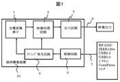
- FIG. 1 is a block diagram showing a configuration example of a solid-state image sensor according to an embodiment.
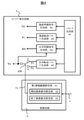
- FIG. 2 is a block diagram showing a configuration example of the timing generation circuit and the control circuit of FIG.
- FIG. 3 is a timing diagram for explaining the period of the horizontal transfer pulse according to the embodiment.
- FIG. 4 is a diagram illustrating an image of an image obtained by an embodiment.
- FIG. 5 is a timing diagram for explaining the horizontal transfer pulse according to the modified example.
- FIG. 6 is a diagram illustrating an image of an image obtained by a modification.
- FIG. 1 is a block diagram showing a configuration example of the solid-state image sensor 10 according to the embodiment.
- FIG. 2 is a block diagram showing a configuration example of the timing generation circuit and the control circuit of FIG.
- FIG. 3 is a timing diagram for explaining the horizontal transfer pulse according to the embodiment.
- FIG. 4 is a diagram illustrating an image of an image obtained by an embodiment.
- the solid-state image pickup device 10 includes a photoelectric conversion element 1, a video processing circuit 2, an output circuit 3, a timing generation circuit 4, and a control circuit 5.
- the photoelectric conversion element 1 is, for example, a solid-state image pickup device such as a CCD (Charge Coupled Device), and is arranged in a matrix in which light incident through an optical system (not shown) is photoelectrically converted and the obtained charge is accumulated.
- Each of the plurality of photodiodes arranged in a matrix can be rephrased as a pixel.
- the video processing circuit 2 converts the transferred electric charge into a video signal
- the output circuit 3 converts the video signal into an interface and outputs the video output signal 6 to the outside of the solid-state imaging device 10.
- the timing generation circuit 4 generates, for example, an exposure start pulse, an exposure end pulse, a vertical synchronization signal, a horizontal synchronization signal, a vertical transfer pulse, a horizontal transfer pulse, and the like to drive the photoelectric conversion element 1 and the image processing circuit 2.
- the operation of the photoelectric conversion element 1 and the operation of the image processing circuit 2 are controlled.
- the control circuit 5 receives an external control signal 7 via RS-232C, IEEE1394, USB2.0, USB3.0, Ethernet, CoaxPress, a switch, or the like, and switches the operation mode of the photoelectric conversion element 1.
- the control circuit 5 determines the period (T) of the horizontal transfer pulse (Th) supplied from the timing generation circuit 4 to the photoelectric conversion element 1 according to the external control signal 7. ,
- the output of the photoelectric conversion element 1 includes a first region (R1) used as the video output signal 6 and a second region (R2) not used as the video output signal 6.
- the period (T) of the horizontal transfer pulse (Th) is the first period (T1) in the first region (R1)
- the period (T) of the horizontal transfer pulse (Th) is the second period (R2) in the second region (R2). It is defined as the period (T2).
- FIG. 2 is a block diagram showing a configuration example of the timing generation circuit and the control circuit of FIG.
- the timing generation circuit 4 includes a pulse generation unit 41, a vertical synchronization signal generation unit 42, a vertical transfer pulse generation unit 43, a horizontal synchronization signal generation unit 44, and a horizontal transfer pulse generation unit 45.
- the pulse generation unit 41 generates a clock pulse.
- the vertical synchronization signal generation unit 42 generates a vertical synchronization signal VS based on the clock pulse.
- One cycle of the vertical synchronization signal VS indicates the period of the video output signal 6 for one frame.
- the charges accumulated in all of the plurality of photodiodes arranged in a matrix are read out, and the video output signal 6 for one frame is generated.
- the vertical transfer pulse generation unit 43 generates a vertical transfer pulse Tv based on the clock pulse and supplies it to the vertical transfer path.
- the horizontal synchronization signal generation unit 44 generates the horizontal synchronization signal HS based on the clock pulse.
- the horizontal synchronization signal HS is generated corresponding to each row of a plurality of photodiodes arranged in a matrix. Therefore, one cycle of the vertical synchronization signal VS includes a plurality of horizontal synchronization signals HS corresponding to the number of rows of the plurality of photodiodes arranged in a matrix.
- the horizontal transfer pulse generation unit 45 generates the horizontal transfer pulse Th based on the clock pulse and supplies it to the horizontal transfer path.
- the horizontal transfer pulse generation unit 45 includes a first terminal a, a second terminal b, and a switch element SW.
- the horizontal transfer pulse Th of the first cycle T1 is generated from the first terminal a
- the horizontal transfer pulse Th of the second cycle T2 (T2> T1) faster than the first cycle T1 is generated from the second terminal b, and the switch element.
- the switch element SW is controlled by the control signal 71 supplied from the control circuit 5.
- the control circuit 5 has a first area range setting unit 51, and the first area range setting unit 51 has a start pixel number setting unit (first setting unit) 52 and an end pixel number setting unit (second setting unit). 53 and.
- the output of the photoelectric conversion element 1 has a first region R1 used as the video output signal 6 and a second region R2 not used as the video output signal 6, and has a first region R1.
- the range of the region is configured to be configurable by the start pixel number setting unit 52 and the end pixel number setting unit 53.
- the start pixel number setting unit 52 the pixel number P1 corresponding to the start position of the first region R1 can be set in the horizontal direction (row direction) of the photoelectric conversion element 1 based on the external control signal 7. .
- the pixel number P2 corresponding to the end position of the first region R1 can be set in the horizontal direction (row direction) of the photoelectric conversion element 1 based on the external control signal 7. ing.
- the first region R1 and the second region R2 can be set as follows.
- First region R1 The region between P1 and P2 is the first region R1 and is an effective portion used as the image output signal 6.
- the effective part can also be said to be an area used as an image.
- Second region R2 The region R21 between P0 and P1 and the region R22 between P2 and P3 are designated as the second region R2, and are unnecessary portions that are not used as the image output signal 6. Unnecessary parts can also be said to be areas that are not used as images.
- the control signal 71 is set to the first level such as a high level so that the switch element SW selects the first terminal a within the range of the first region R1.
- the control signal 71 is set to a second level such as a low level so that the switch element SW selects the second terminal b within the range of the second region R2.
- the period T of the horizontal transfer pulse Th is the cycle T1 of the normal transfer. And transfer the pixel of the photoelectric conversion element 1.
- the period T of the horizontal transfer pulse Th is set to the second period T2, which is faster than the first period T1, and the pixels of the photoelectric conversion element 1 are transferred. That is, in the horizontal high-speed transfer periods 27 and 28, the period T of the horizontal transfer pulse Th is set to high speed (second period T2). From the solid-state image sensor 10, only the video output 29 corresponding to the first region R1 is output as the video output signal 6.
- the horizontal synchronization signal HS having one horizontal period 26 the one horizontal period 26 is shortened by the amount that the horizontal transfer pulse Th is increased, so that the frame rate defined as the number of frames output per second is defined as the frame rate. It gets higher.
- FIG. 4 is an image image when the horizontal transfer pulse Th is set at high speed.
- the solid-state imaging device 10 acquires an image in a range of a vertically effective area 91 which is the number of arrangements (number of rows) of pixels in the vertical direction and a horizontally effective area 95 which is the number of arrangements (number of columns) of pixels in the horizontal direction. It shall be possible.
- a vertically effective area 91 which is the number of arrangements (number of rows) of pixels in the vertical direction
- a horizontally effective area 95 which is the number of arrangements (number of columns) of pixels in the horizontal direction. It shall be possible.
- the first pixel number P0, the pixel number P1 corresponding to the start position of the first region R1, and the pixel number P2 corresponding to the end position of the first region R1 are shown.
- the last pixel number P3 are drawn.
- the image pickup object 96 which is the subject, considers, for example, a subject such as a ball that falls or moves in the vertical direction.
- the image pickup object 96 exists only in the first region R1. Therefore, since the image pickup object 96 exists only in the first region R1, the first region R1 is defined as an effective portion used as an image, and the video output 29 of the first region R1 is used as a video output signal 6 from the solid-state image sensor 10. Output.
- the second region R2 is defined as an unnecessary portion that is not used as an image, and the image corresponding to the second region R2 is not output from the solid-state image sensor 10.
- a region such as the first region R1 that is, the vertical direction is the same as the number of pixels arranged in the vertical direction of the solid-state imaging device 10, and the horizontal direction is the arrangement of the pixels in the horizontal direction of the solid-state imaging device 10. Reading a video signal from a region smaller than the number (that is, reading the video output 29 in FIG. 3) is referred to as a horizontal partial scan method.
- the horizontal period of the first region R1 (the number of pixels in the horizontal direction: the number of pixels between P1 and P2) is based on the number of pixels in the horizontal direction of the solid-state imaging device 10 (the number of pixels between P0 and P3). By shortening the length, only the necessary image can be obtained and the frame rate can be increased.
- FIG. 5 is a timing diagram for explaining the horizontal transfer pulse according to the modified example.
- FIG. 6 is a diagram illustrating an image of an image obtained by a modification.
- FIG. 5 is different from FIG. 3 in that the horizontal high-speed transfer period 28a shown in FIG. 5 is longer than the horizontal high-speed transfer period 28 shown in FIG. 3, and the normal transfer period 31a shown in FIG. 5 is shown in FIG. The point is that it is shorter than the normal transfer period 31.
- the output data amount of the video output 29a is also reduced as compared with the output data amount of the video output 29 of FIG.
- the horizontal high-speed transfer period 27 may be changed, of course.
- FIG. 6 The difference between FIG. 6 and FIG. 4 is that in FIG. 6, the pixel number P1a indicating the start position of the first region R1a has been changed. As a result, the horizontal period of the region R21a shown in FIG. 6 becomes longer than the horizontal period of the region R21 shown in FIG. 4, and the horizontal period of the first region R1a shown in FIG. 6 is shown in FIG. It is shortened as compared with the horizontal period of the first region R1 shown.
- the horizontal high-speed transfer period 27 and 28a are larger than the normal transfer period 31a, the period Ths of the horizontal synchronization signal HS is shortened accordingly, so that the frame rate becomes higher.
- the video output of only the necessary part can be obtained, and the frame rate can be increased.
- the frame rate when the frame rate is insufficient even if the partial scan is used, the frame rate can be further increased by using the present invention.
- the capture position of the portion used as an image (imaging area: R1) can be changed, the imaging area (R1a) can be followed even if the imaging object 96 moves laterally.
- a solid-state image pickup device 3CCD, etc.
- a solid-state image sensor that uses the photoelectric conversion element of the above and a solid-state image sensor that uses a monochrome photoelectric conversion element.
- Photoelectric conversion element 2 Video processing circuit 3: Output circuit 4: Timing generation circuit 5: Control circuit 6: Video output 7: External control signal 10: Solid-state image sensor 51: First area range setting unit 52: Start pixel number Setting unit 53: End pixel number setting unit Th: Horizontal transfer pulse R1, R1a: First area R2, R21, R21a, R22: Second area
Landscapes
- Engineering & Computer Science (AREA)
- Multimedia (AREA)
- Signal Processing (AREA)
- Transforming Light Signals Into Electric Signals (AREA)
Priority Applications (1)
| Application Number | Priority Date | Filing Date | Title |
|---|---|---|---|
| JP2022547422A JP7438379B2 (ja) | 2020-09-09 | 2021-07-16 | 撮像装置 |
Applications Claiming Priority (2)
| Application Number | Priority Date | Filing Date | Title |
|---|---|---|---|
| JP2020150922 | 2020-09-09 | ||
| JP2020-150922 | 2020-09-09 |
Publications (1)
| Publication Number | Publication Date |
|---|---|
| WO2022054405A1 true WO2022054405A1 (ja) | 2022-03-17 |
Family
ID=80632494
Family Applications (1)
| Application Number | Title | Priority Date | Filing Date |
|---|---|---|---|
| PCT/JP2021/026766 Ceased WO2022054405A1 (ja) | 2020-09-09 | 2021-07-16 | 撮像装置 |
Country Status (2)
| Country | Link |
|---|---|
| JP (1) | JP7438379B2 (https=) |
| WO (1) | WO2022054405A1 (https=) |
Citations (5)
| Publication number | Priority date | Publication date | Assignee | Title |
|---|---|---|---|---|
| JPH11191863A (ja) * | 1997-04-02 | 1999-07-13 | Canon Inc | 固体撮像装置、固体撮像装置の駆動方法、固体撮像素子および固体撮像素子の駆動方法 |
| JP2002271702A (ja) * | 2001-03-13 | 2002-09-20 | Hitachi Kokusai Electric Inc | 固体撮像装置 |
| JP2004363654A (ja) * | 2003-05-30 | 2004-12-24 | Hitachi Kokusai Electric Inc | テレビジョンカメラ |
| JP2008042838A (ja) * | 2006-08-10 | 2008-02-21 | Hitachi Kokusai Electric Inc | テレビジョンカメラ |
| JP2012044296A (ja) * | 2010-08-16 | 2012-03-01 | Fujitsu Semiconductor Ltd | 画像処理装置 |
-
2021
- 2021-07-16 JP JP2022547422A patent/JP7438379B2/ja active Active
- 2021-07-16 WO PCT/JP2021/026766 patent/WO2022054405A1/ja not_active Ceased
Patent Citations (5)
| Publication number | Priority date | Publication date | Assignee | Title |
|---|---|---|---|---|
| JPH11191863A (ja) * | 1997-04-02 | 1999-07-13 | Canon Inc | 固体撮像装置、固体撮像装置の駆動方法、固体撮像素子および固体撮像素子の駆動方法 |
| JP2002271702A (ja) * | 2001-03-13 | 2002-09-20 | Hitachi Kokusai Electric Inc | 固体撮像装置 |
| JP2004363654A (ja) * | 2003-05-30 | 2004-12-24 | Hitachi Kokusai Electric Inc | テレビジョンカメラ |
| JP2008042838A (ja) * | 2006-08-10 | 2008-02-21 | Hitachi Kokusai Electric Inc | テレビジョンカメラ |
| JP2012044296A (ja) * | 2010-08-16 | 2012-03-01 | Fujitsu Semiconductor Ltd | 画像処理装置 |
Also Published As
| Publication number | Publication date |
|---|---|
| JP7438379B2 (ja) | 2024-02-26 |
| JPWO2022054405A1 (https=) | 2022-03-17 |
Similar Documents
| Publication | Publication Date | Title |
|---|---|---|
| US8659691B2 (en) | Solid-state imaging apparatus, imaging system, and drive method of solid-state imaging apparatus | |
| TWI394448B (zh) | 固態成像裝置,成像裝置及固態成像裝置之驅動方法 | |
| JP7473041B2 (ja) | 撮像素子、及び撮像装置 | |
| EP1940148A2 (en) | Solid-state image sensor and imaging system | |
| CN101753859B (zh) | 摄像传感器及其驱动方法和摄像设备 | |
| US7675559B2 (en) | Image sensing apparatus having a two step transfer operation and method of controlling same | |
| US20150281610A1 (en) | Solid-state imaging apparatus and imaging system | |
| KR20110019725A (ko) | 고체 촬상 소자 및 카메라 시스템 | |
| KR101080568B1 (ko) | 고체 촬상 장치 및 카메라 시스템 | |
| CN117678233A (zh) | 摄像元件以及摄像装置 | |
| US11716554B2 (en) | Solid-state imaging device and method for driving the same, and electronic apparatus | |
| US8300122B2 (en) | Solid-state imaging device, camera system, and signal reading method | |
| US20120262613A1 (en) | Solid-state imaging apparatus | |
| KR20140107212A (ko) | 고체 촬상 소자 및 그 구동 방법, 카메라 시스템 | |
| EP4109886B1 (en) | Imaging element and imaging device | |
| WO2009087726A1 (ja) | 撮像装置 | |
| US11252354B2 (en) | Image sensor, control method thereof, and image capturing apparatus | |
| JP7438379B2 (ja) | 撮像装置 | |
| US12382200B2 (en) | Image capturing circuit that can be applied to image capturing apparatus | |
| US11368610B2 (en) | Image capture apparatus and control method therefor | |
| JP2007166486A (ja) | 固体撮像装置 | |
| JP2017034508A (ja) | 撮像素子及びその制御方法、及び、撮像装置 | |
| JP2016103701A (ja) | 撮像素子及びその制御方法 | |
| JP7315054B2 (ja) | 撮像素子および撮像装置 | |
| US20250184598A1 (en) | Image capturing apparatus |
Legal Events
| Date | Code | Title | Description |
|---|---|---|---|
| 121 | Ep: the epo has been informed by wipo that ep was designated in this application |
Ref document number: 21866365 Country of ref document: EP Kind code of ref document: A1 |
|
| ENP | Entry into the national phase |
Ref document number: 2022547422 Country of ref document: JP Kind code of ref document: A |
|
| NENP | Non-entry into the national phase |
Ref country code: DE |
|
| 122 | Ep: pct application non-entry in european phase |
Ref document number: 21866365 Country of ref document: EP Kind code of ref document: A1 |