WO2022050321A1 - Liquid crystal diffraction element, optical element, image display unit, head-mounted display, beam steering, and sensor - Google Patents
Liquid crystal diffraction element, optical element, image display unit, head-mounted display, beam steering, and sensor Download PDFInfo
- Publication number
- WO2022050321A1 WO2022050321A1 PCT/JP2021/032179 JP2021032179W WO2022050321A1 WO 2022050321 A1 WO2022050321 A1 WO 2022050321A1 JP 2021032179 W JP2021032179 W JP 2021032179W WO 2022050321 A1 WO2022050321 A1 WO 2022050321A1
- Authority
- WO
- WIPO (PCT)
- Prior art keywords
- liquid crystal
- optically anisotropic
- anisotropic layer
- light
- crystal compound
- Prior art date
Links
- 239000004973 liquid crystal related substance Substances 0.000 title claims abstract description 878
- 230000003287 optical effect Effects 0.000 title claims abstract description 262
- 150000001875 compounds Chemical class 0.000 claims abstract description 246
- 239000000203 mixture Substances 0.000 claims description 91
- VYPSYNLAJGMNEJ-UHFFFAOYSA-N Silicium dioxide Chemical compound O=[Si]=O VYPSYNLAJGMNEJ-UHFFFAOYSA-N 0.000 claims description 21
- 229910052814 silicon oxide Inorganic materials 0.000 claims description 19
- 239000010410 layer Substances 0.000 description 665
- 239000010408 film Substances 0.000 description 205
- HUWSZNZAROKDRZ-RRLWZMAJSA-N (3r,4r)-3-azaniumyl-5-[[(2s,3r)-1-[(2s)-2,3-dicarboxypyrrolidin-1-yl]-3-methyl-1-oxopentan-2-yl]amino]-5-oxo-4-sulfanylpentane-1-sulfonate Chemical compound OS(=O)(=O)CC[C@@H](N)[C@@H](S)C(=O)N[C@@H]([C@H](C)CC)C(=O)N1CCC(C(O)=O)[C@H]1C(O)=O HUWSZNZAROKDRZ-RRLWZMAJSA-N 0.000 description 70
- UWCWUCKPEYNDNV-LBPRGKRZSA-N 2,6-dimethyl-n-[[(2s)-pyrrolidin-2-yl]methyl]aniline Chemical compound CC1=CC=CC(C)=C1NC[C@H]1NCCC1 UWCWUCKPEYNDNV-LBPRGKRZSA-N 0.000 description 62
- 230000010287 polarization Effects 0.000 description 58
- 238000000034 method Methods 0.000 description 42
- 239000000853 adhesive Substances 0.000 description 39
- 230000001070 adhesive effect Effects 0.000 description 39
- 230000000737 periodic effect Effects 0.000 description 34
- 238000011156 evaluation Methods 0.000 description 32
- 238000004519 manufacturing process Methods 0.000 description 30
- 230000000052 comparative effect Effects 0.000 description 27
- 239000011521 glass Substances 0.000 description 25
- 239000000463 material Substances 0.000 description 24
- 230000015572 biosynthetic process Effects 0.000 description 22
- 238000000576 coating method Methods 0.000 description 21
- 238000001878 scanning electron micrograph Methods 0.000 description 20
- 239000011248 coating agent Substances 0.000 description 19
- 239000012790 adhesive layer Substances 0.000 description 18
- 239000000758 substrate Substances 0.000 description 18
- 238000010521 absorption reaction Methods 0.000 description 17
- ZWEHNKRNPOVVGH-UHFFFAOYSA-N 2-Butanone Chemical compound CCC(C)=O ZWEHNKRNPOVVGH-UHFFFAOYSA-N 0.000 description 15
- 230000001965 increasing effect Effects 0.000 description 15
- 125000004432 carbon atom Chemical group C* 0.000 description 14
- 239000003795 chemical substances by application Substances 0.000 description 14
- 238000010586 diagram Methods 0.000 description 13
- -1 polyethylene terephthalate Polymers 0.000 description 13
- 239000004372 Polyvinyl alcohol Substances 0.000 description 9
- 238000005520 cutting process Methods 0.000 description 9
- 229920002451 polyvinyl alcohol Polymers 0.000 description 9
- 125000001424 substituent group Chemical group 0.000 description 9
- ZCSHACFHMFHFKK-UHFFFAOYSA-N 2-methyl-1,3,5-trinitrobenzene;2,4,6-trinitro-1,3,5-triazinane Chemical compound [O-][N+](=O)C1NC([N+]([O-])=O)NC([N+]([O-])=O)N1.CC1=C([N+]([O-])=O)C=C([N+]([O-])=O)C=C1[N+]([O-])=O ZCSHACFHMFHFKK-UHFFFAOYSA-N 0.000 description 8
- 125000004435 hydrogen atom Chemical group [H]* 0.000 description 8
- 229920000642 polymer Polymers 0.000 description 8
- 230000008859 change Effects 0.000 description 7
- 238000010438 heat treatment Methods 0.000 description 7
- 230000031700 light absorption Effects 0.000 description 7
- 239000003505 polymerization initiator Substances 0.000 description 7
- 238000012662 bulk polymerization Methods 0.000 description 6
- 239000007788 liquid Substances 0.000 description 6
- 238000007740 vapor deposition Methods 0.000 description 6
- 230000009471 action Effects 0.000 description 5
- 238000009826 distribution Methods 0.000 description 5
- 230000000694 effects Effects 0.000 description 5
- 230000001678 irradiating effect Effects 0.000 description 5
- 238000010030 laminating Methods 0.000 description 5
- 239000002253 acid Substances 0.000 description 4
- 229910052799 carbon Inorganic materials 0.000 description 4
- 238000005336 cracking Methods 0.000 description 4
- 230000028161 membrane depolarization Effects 0.000 description 4
- 239000011241 protective layer Substances 0.000 description 4
- 239000000126 substance Substances 0.000 description 4
- 238000012546 transfer Methods 0.000 description 4
- 239000006097 ultraviolet radiation absorber Substances 0.000 description 4
- ODIGIKRIUKFKHP-UHFFFAOYSA-N (n-propan-2-yloxycarbonylanilino) acetate Chemical compound CC(C)OC(=O)N(OC(C)=O)C1=CC=CC=C1 ODIGIKRIUKFKHP-UHFFFAOYSA-N 0.000 description 3
- ZCYVEMRRCGMTRW-UHFFFAOYSA-N 7553-56-2 Chemical compound [I] ZCYVEMRRCGMTRW-UHFFFAOYSA-N 0.000 description 3
- WVDDGKGOMKODPV-UHFFFAOYSA-N Benzyl alcohol Chemical compound OCC1=CC=CC=C1 WVDDGKGOMKODPV-UHFFFAOYSA-N 0.000 description 3
- 239000004642 Polyimide Substances 0.000 description 3
- 239000002250 absorbent Substances 0.000 description 3
- 230000002745 absorbent Effects 0.000 description 3
- 230000004075 alteration Effects 0.000 description 3
- 230000008901 benefit Effects 0.000 description 3
- 239000001913 cellulose Substances 0.000 description 3
- 229920002678 cellulose Polymers 0.000 description 3
- 239000011247 coating layer Substances 0.000 description 3
- 229910052740 iodine Inorganic materials 0.000 description 3
- 239000011630 iodine Substances 0.000 description 3
- 238000006317 isomerization reaction Methods 0.000 description 3
- 239000012788 optical film Substances 0.000 description 3
- 238000009832 plasma treatment Methods 0.000 description 3
- 229920001721 polyimide Polymers 0.000 description 3
- 238000012545 processing Methods 0.000 description 3
- 239000011347 resin Substances 0.000 description 3
- 229920005989 resin Polymers 0.000 description 3
- NIXOWILDQLNWCW-UHFFFAOYSA-M Acrylate Chemical compound [O-]C(=O)C=C NIXOWILDQLNWCW-UHFFFAOYSA-M 0.000 description 2
- 239000005264 High molar mass liquid crystal Substances 0.000 description 2
- KLDXJTOLSGUMSJ-JGWLITMVSA-N Isosorbide Chemical compound O[C@@H]1CO[C@@H]2[C@@H](O)CO[C@@H]21 KLDXJTOLSGUMSJ-JGWLITMVSA-N 0.000 description 2
- PXHVJJICTQNCMI-UHFFFAOYSA-N Nickel Chemical compound [Ni] PXHVJJICTQNCMI-UHFFFAOYSA-N 0.000 description 2
- 239000004952 Polyamide Substances 0.000 description 2
- 239000004820 Pressure-sensitive adhesive Substances 0.000 description 2
- 229910004298 SiO 2 Inorganic materials 0.000 description 2
- WYURNTSHIVDZCO-UHFFFAOYSA-N Tetrahydrofuran Chemical compound C1CCOC1 WYURNTSHIVDZCO-UHFFFAOYSA-N 0.000 description 2
- MCMNRKCIXSYSNV-UHFFFAOYSA-N Zirconium dioxide Chemical compound O=[Zr]=O MCMNRKCIXSYSNV-UHFFFAOYSA-N 0.000 description 2
- 150000001252 acrylic acid derivatives Chemical class 0.000 description 2
- NIXOWILDQLNWCW-UHFFFAOYSA-N acrylic acid group Chemical group C(C=C)(=O)O NIXOWILDQLNWCW-UHFFFAOYSA-N 0.000 description 2
- 125000000217 alkyl group Chemical group 0.000 description 2
- 238000013459 approach Methods 0.000 description 2
- 238000000149 argon plasma sintering Methods 0.000 description 2
- 125000000751 azo group Chemical group [*]N=N[*] 0.000 description 2
- 125000005337 azoxy group Chemical group [N+]([O-])(=N*)* 0.000 description 2
- 230000004888 barrier function Effects 0.000 description 2
- 239000000919 ceramic Substances 0.000 description 2
- 150000001788 chalcone derivatives Chemical class 0.000 description 2
- 125000004093 cyano group Chemical group *C#N 0.000 description 2
- BGTOWKSIORTVQH-UHFFFAOYSA-N cyclopentanone Chemical compound O=C1CCCC1 BGTOWKSIORTVQH-UHFFFAOYSA-N 0.000 description 2
- 238000006471 dimerization reaction Methods 0.000 description 2
- 238000004043 dyeing Methods 0.000 description 2
- 238000005516 engineering process Methods 0.000 description 2
- 150000002148 esters Chemical class 0.000 description 2
- 239000007789 gas Substances 0.000 description 2
- 125000002887 hydroxy group Chemical group [H]O* 0.000 description 2
- 238000003384 imaging method Methods 0.000 description 2
- 230000001939 inductive effect Effects 0.000 description 2
- 229960002479 isosorbide Drugs 0.000 description 2
- 125000005647 linker group Chemical group 0.000 description 2
- 238000005259 measurement Methods 0.000 description 2
- 239000012528 membrane Substances 0.000 description 2
- QSHDDOUJBYECFT-UHFFFAOYSA-N mercury Chemical compound [Hg] QSHDDOUJBYECFT-UHFFFAOYSA-N 0.000 description 2
- 229910052753 mercury Inorganic materials 0.000 description 2
- 150000002894 organic compounds Chemical class 0.000 description 2
- 229910052760 oxygen Inorganic materials 0.000 description 2
- 230000002341 photoisomerizing effect Effects 0.000 description 2
- 229920002647 polyamide Polymers 0.000 description 2
- 229920000139 polyethylene terephthalate Polymers 0.000 description 2
- 239000005020 polyethylene terephthalate Substances 0.000 description 2
- 238000006116 polymerization reaction Methods 0.000 description 2
- 239000000843 powder Substances 0.000 description 2
- 108010001861 pregnancy-associated glycoprotein 1 Proteins 0.000 description 2
- 230000002441 reversible effect Effects 0.000 description 2
- 239000002356 single layer Substances 0.000 description 2
- 150000003384 small molecules Chemical class 0.000 description 2
- 239000002904 solvent Substances 0.000 description 2
- 229910052717 sulfur Inorganic materials 0.000 description 2
- 239000004094 surface-active agent Substances 0.000 description 2
- WBYWAXJHAXSJNI-VOTSOKGWSA-M trans-cinnamate Chemical class [O-]C(=O)\C=C\C1=CC=CC=C1 WBYWAXJHAXSJNI-VOTSOKGWSA-M 0.000 description 2
- 238000001771 vacuum deposition Methods 0.000 description 2
- KLDXJTOLSGUMSJ-BXKVDMCESA-N (3s,3as,6s,6as)-2,3,3a,5,6,6a-hexahydrofuro[3,2-b]furan-3,6-diol Chemical class O[C@H]1CO[C@H]2[C@@H](O)CO[C@H]21 KLDXJTOLSGUMSJ-BXKVDMCESA-N 0.000 description 1
- ARXJGSRGQADJSQ-UHFFFAOYSA-N 1-methoxypropan-2-ol Chemical compound COCC(C)O ARXJGSRGQADJSQ-UHFFFAOYSA-N 0.000 description 1
- AUXIEQKHXAYAHG-UHFFFAOYSA-N 1-phenylcyclohexane-1-carbonitrile Chemical class C=1C=CC=CC=1C1(C#N)CCCCC1 AUXIEQKHXAYAHG-UHFFFAOYSA-N 0.000 description 1
- OOLUVSIJOMLOCB-UHFFFAOYSA-N 1633-22-3 Chemical compound C1CC(C=C2)=CC=C2CCC2=CC=C1C=C2 OOLUVSIJOMLOCB-UHFFFAOYSA-N 0.000 description 1
- BBBUAWSVILPJLL-UHFFFAOYSA-N 2-(2-ethylhexoxymethyl)oxirane Chemical compound CCCCC(CC)COCC1CO1 BBBUAWSVILPJLL-UHFFFAOYSA-N 0.000 description 1
- SHKUUQIDMUMQQK-UHFFFAOYSA-N 2-[4-(oxiran-2-ylmethoxy)butoxymethyl]oxirane Chemical compound C1OC1COCCCCOCC1CO1 SHKUUQIDMUMQQK-UHFFFAOYSA-N 0.000 description 1
- POAOYUHQDCAZBD-UHFFFAOYSA-N 2-butoxyethanol Chemical compound CCCCOCCO POAOYUHQDCAZBD-UHFFFAOYSA-N 0.000 description 1
- WLNDDIWESXCXHM-UHFFFAOYSA-N 2-phenyl-1,4-dioxane Chemical class C1OCCOC1C1=CC=CC=C1 WLNDDIWESXCXHM-UHFFFAOYSA-N 0.000 description 1
- OXPDQFOKSZYEMJ-UHFFFAOYSA-N 2-phenylpyrimidine Chemical class C1=CC=CC=C1C1=NC=CC=N1 OXPDQFOKSZYEMJ-UHFFFAOYSA-N 0.000 description 1
- 239000004925 Acrylic resin Substances 0.000 description 1
- 229920002284 Cellulose triacetate Polymers 0.000 description 1
- 239000004986 Cholesteric liquid crystals (ChLC) Substances 0.000 description 1
- 239000004821 Contact adhesive Substances 0.000 description 1
- 229920000089 Cyclic olefin copolymer Polymers 0.000 description 1
- 239000004593 Epoxy Substances 0.000 description 1
- 239000004831 Hot glue Substances 0.000 description 1
- PEEHTFAAVSWFBL-UHFFFAOYSA-N Maleimide Chemical compound O=C1NC(=O)C=C1 PEEHTFAAVSWFBL-UHFFFAOYSA-N 0.000 description 1
- 229920000877 Melamine resin Polymers 0.000 description 1
- CERQOIWHTDAKMF-UHFFFAOYSA-M Methacrylate Chemical compound CC(=C)C([O-])=O CERQOIWHTDAKMF-UHFFFAOYSA-M 0.000 description 1
- NTIZESTWPVYFNL-UHFFFAOYSA-N Methyl isobutyl ketone Chemical compound CC(C)CC(C)=O NTIZESTWPVYFNL-UHFFFAOYSA-N 0.000 description 1
- UIHCLUNTQKBZGK-UHFFFAOYSA-N Methyl isobutyl ketone Natural products CCC(C)C(C)=O UIHCLUNTQKBZGK-UHFFFAOYSA-N 0.000 description 1
- CTQNGGLPUBDAKN-UHFFFAOYSA-N O-Xylene Chemical compound CC1=CC=CC=C1C CTQNGGLPUBDAKN-UHFFFAOYSA-N 0.000 description 1
- NNLVGZFZQQXQNW-ADJNRHBOSA-N [(2r,3r,4s,5r,6s)-4,5-diacetyloxy-3-[(2s,3r,4s,5r,6r)-3,4,5-triacetyloxy-6-(acetyloxymethyl)oxan-2-yl]oxy-6-[(2r,3r,4s,5r,6s)-4,5,6-triacetyloxy-2-(acetyloxymethyl)oxan-3-yl]oxyoxan-2-yl]methyl acetate Chemical compound O([C@@H]1O[C@@H]([C@H]([C@H](OC(C)=O)[C@H]1OC(C)=O)O[C@H]1[C@@H]([C@@H](OC(C)=O)[C@H](OC(C)=O)[C@@H](COC(C)=O)O1)OC(C)=O)COC(=O)C)[C@@H]1[C@@H](COC(C)=O)O[C@@H](OC(C)=O)[C@H](OC(C)=O)[C@H]1OC(C)=O NNLVGZFZQQXQNW-ADJNRHBOSA-N 0.000 description 1
- 239000006096 absorbing agent Substances 0.000 description 1
- 125000003647 acryloyl group Chemical group O=C([*])C([H])=C([H])[H] 0.000 description 1
- 125000002252 acyl group Chemical group 0.000 description 1
- 125000004423 acyloxy group Chemical group 0.000 description 1
- 125000001931 aliphatic group Chemical group 0.000 description 1
- 125000005236 alkanoylamino group Chemical group 0.000 description 1
- 125000003545 alkoxy group Chemical group 0.000 description 1
- 125000004453 alkoxycarbonyl group Chemical group 0.000 description 1
- 125000004457 alkyl amino carbonyl group Chemical group 0.000 description 1
- 125000003282 alkyl amino group Chemical group 0.000 description 1
- 125000004691 alkyl thio carbonyl group Chemical group 0.000 description 1
- 125000004414 alkyl thio group Chemical group 0.000 description 1
- 125000003368 amide group Chemical group 0.000 description 1
- 125000003277 amino group Chemical group 0.000 description 1
- 239000007864 aqueous solution Substances 0.000 description 1
- 125000006615 aromatic heterocyclic group Chemical group 0.000 description 1
- 125000002029 aromatic hydrocarbon group Chemical group 0.000 description 1
- 125000003118 aryl group Chemical group 0.000 description 1
- 230000003190 augmentative effect Effects 0.000 description 1
- 125000004069 aziridinyl group Chemical group 0.000 description 1
- 238000005452 bending Methods 0.000 description 1
- 150000001558 benzoic acid derivatives Chemical class 0.000 description 1
- 150000008366 benzophenones Chemical class 0.000 description 1
- 125000003354 benzotriazolyl group Chemical class N1N=NC2=C1C=CC=C2* 0.000 description 1
- 235000019445 benzyl alcohol Nutrition 0.000 description 1
- ZDZHCHYQNPQSGG-UHFFFAOYSA-N binaphthyl group Chemical group C1(=CC=CC2=CC=CC=C12)C1=CC=CC2=CC=CC=C12 ZDZHCHYQNPQSGG-UHFFFAOYSA-N 0.000 description 1
- 230000000903 blocking effect Effects 0.000 description 1
- 150000001639 boron compounds Chemical class 0.000 description 1
- 125000003178 carboxy group Chemical group [H]OC(*)=O 0.000 description 1
- 239000012461 cellulose resin Substances 0.000 description 1
- 238000006243 chemical reaction Methods 0.000 description 1
- 239000003153 chemical reaction reagent Substances 0.000 description 1
- 239000003086 colorant Substances 0.000 description 1
- 239000000470 constituent Substances 0.000 description 1
- 238000003851 corona treatment Methods 0.000 description 1
- 125000000332 coumarinyl group Chemical class O1C(=O)C(=CC2=CC=CC=C12)* 0.000 description 1
- 239000013078 crystal Substances 0.000 description 1
- NLCKLZIHJQEMCU-UHFFFAOYSA-N cyano prop-2-enoate Chemical class C=CC(=O)OC#N NLCKLZIHJQEMCU-UHFFFAOYSA-N 0.000 description 1
- 125000004802 cyanophenyl group Chemical group 0.000 description 1
- 230000007423 decrease Effects 0.000 description 1
- 238000000151 deposition Methods 0.000 description 1
- 238000001514 detection method Methods 0.000 description 1
- 230000006866 deterioration Effects 0.000 description 1
- 238000001035 drying Methods 0.000 description 1
- 239000000428 dust Substances 0.000 description 1
- 239000000839 emulsion Substances 0.000 description 1
- 125000003700 epoxy group Chemical group 0.000 description 1
- 230000001747 exhibiting effect Effects 0.000 description 1
- 239000004744 fabric Substances 0.000 description 1
- 239000010419 fine particle Substances 0.000 description 1
- 229910052731 fluorine Inorganic materials 0.000 description 1
- 125000001153 fluoro group Chemical group F* 0.000 description 1
- 239000006260 foam Substances 0.000 description 1
- 210000000873 fovea centralis Anatomy 0.000 description 1
- 125000005843 halogen group Chemical group 0.000 description 1
- UOYPNWSDSPYOSN-UHFFFAOYSA-N hexahelicene Chemical compound C1=CC=CC2=C(C=3C(=CC=C4C=CC=5C(C=34)=CC=CC=5)C=C3)C3=CC=C21 UOYPNWSDSPYOSN-UHFFFAOYSA-N 0.000 description 1
- 239000003999 initiator Substances 0.000 description 1
- 150000002484 inorganic compounds Chemical class 0.000 description 1
- 229910010272 inorganic material Inorganic materials 0.000 description 1
- 239000004816 latex Substances 0.000 description 1
- 229920000126 latex Polymers 0.000 description 1
- 239000013521 mastic Substances 0.000 description 1
- JDSHMPZPIAZGSV-UHFFFAOYSA-N melamine Chemical compound NC1=NC(N)=NC(N)=N1 JDSHMPZPIAZGSV-UHFFFAOYSA-N 0.000 description 1
- 239000000113 methacrylic resin Substances 0.000 description 1
- 125000002496 methyl group Chemical group [H]C([H])([H])* 0.000 description 1
- 238000002156 mixing Methods 0.000 description 1
- 230000004048 modification Effects 0.000 description 1
- 238000012986 modification Methods 0.000 description 1
- 238000000465 moulding Methods 0.000 description 1
- IZXDTJXEUISVAJ-UHFFFAOYSA-N n-methyl-n-octadecyloctadecan-1-amine;hydrochloride Chemical compound [Cl-].CCCCCCCCCCCCCCCCCC[NH+](C)CCCCCCCCCCCCCCCCCC IZXDTJXEUISVAJ-UHFFFAOYSA-N 0.000 description 1
- 229910052759 nickel Inorganic materials 0.000 description 1
- 125000000449 nitro group Chemical group [O-][N+](*)=O 0.000 description 1
- 239000012299 nitrogen atmosphere Substances 0.000 description 1
- 239000003960 organic solvent Substances 0.000 description 1
- 235000012771 pancakes Nutrition 0.000 description 1
- 238000000059 patterning Methods 0.000 description 1
- OPYYWWIJPHKUDZ-UHFFFAOYSA-N phenyl cyclohexanecarboxylate Chemical class C1CCCCC1C(=O)OC1=CC=CC=C1 OPYYWWIJPHKUDZ-UHFFFAOYSA-N 0.000 description 1
- 229920003023 plastic Polymers 0.000 description 1
- 239000004033 plastic Substances 0.000 description 1
- 229920003229 poly(methyl methacrylate) Polymers 0.000 description 1
- 239000004417 polycarbonate Substances 0.000 description 1
- 229920000515 polycarbonate Polymers 0.000 description 1
- 150000004291 polyenes Chemical class 0.000 description 1
- 229920000728 polyester Polymers 0.000 description 1
- 229920006254 polymer film Polymers 0.000 description 1
- 239000004926 polymethyl methacrylate Substances 0.000 description 1
- 239000004800 polyvinyl chloride Substances 0.000 description 1
- 229920000915 polyvinyl chloride Polymers 0.000 description 1
- 238000002360 preparation method Methods 0.000 description 1
- 230000001681 protective effect Effects 0.000 description 1
- 238000007127 saponification reaction Methods 0.000 description 1
- 230000003678 scratch resistant effect Effects 0.000 description 1
- 230000001568 sexual effect Effects 0.000 description 1
- 238000004904 shortening Methods 0.000 description 1
- 150000004756 silanes Chemical class 0.000 description 1
- 239000000377 silicon dioxide Substances 0.000 description 1
- LIVNPJMFVYWSIS-UHFFFAOYSA-N silicon monoxide Chemical compound [Si-]#[O+] LIVNPJMFVYWSIS-UHFFFAOYSA-N 0.000 description 1
- 238000004528 spin coating Methods 0.000 description 1
- 238000003892 spreading Methods 0.000 description 1
- 230000007480 spreading Effects 0.000 description 1
- 125000000020 sulfo group Chemical group O=S(=O)([*])O[H] 0.000 description 1
- 230000003746 surface roughness Effects 0.000 description 1
- YLQBMQCUIZJEEH-UHFFFAOYSA-N tetrahydrofuran Natural products C=1C=COC=1 YLQBMQCUIZJEEH-UHFFFAOYSA-N 0.000 description 1
- 229920001169 thermoplastic Polymers 0.000 description 1
- 239000004416 thermosoftening plastic Substances 0.000 description 1
- 125000003396 thiol group Chemical group [H]S* 0.000 description 1
- 238000002834 transmittance Methods 0.000 description 1
- XLYOFNOQVPJJNP-UHFFFAOYSA-N water Substances O XLYOFNOQVPJJNP-UHFFFAOYSA-N 0.000 description 1
- 239000008096 xylene Substances 0.000 description 1
Images


Classifications
-
- G—PHYSICS
- G02—OPTICS
- G02F—OPTICAL DEVICES OR ARRANGEMENTS FOR THE CONTROL OF LIGHT BY MODIFICATION OF THE OPTICAL PROPERTIES OF THE MEDIA OF THE ELEMENTS INVOLVED THEREIN; NON-LINEAR OPTICS; FREQUENCY-CHANGING OF LIGHT; OPTICAL LOGIC ELEMENTS; OPTICAL ANALOGUE/DIGITAL CONVERTERS
- G02F1/00—Devices or arrangements for the control of the intensity, colour, phase, polarisation or direction of light arriving from an independent light source, e.g. switching, gating or modulating; Non-linear optics
- G02F1/29—Devices or arrangements for the control of the intensity, colour, phase, polarisation or direction of light arriving from an independent light source, e.g. switching, gating or modulating; Non-linear optics for the control of the position or the direction of light beams, i.e. deflection
- G02F1/292—Devices or arrangements for the control of the intensity, colour, phase, polarisation or direction of light arriving from an independent light source, e.g. switching, gating or modulating; Non-linear optics for the control of the position or the direction of light beams, i.e. deflection by controlled diffraction or phased-array beam steering
-
- G—PHYSICS
- G02—OPTICS
- G02B—OPTICAL ELEMENTS, SYSTEMS OR APPARATUS
- G02B5/00—Optical elements other than lenses
- G02B5/18—Diffraction gratings
-
- G—PHYSICS
- G02—OPTICS
- G02B—OPTICAL ELEMENTS, SYSTEMS OR APPARATUS
- G02B5/00—Optical elements other than lenses
- G02B5/30—Polarising elements
-
- G—PHYSICS
- G02—OPTICS
- G02F—OPTICAL DEVICES OR ARRANGEMENTS FOR THE CONTROL OF LIGHT BY MODIFICATION OF THE OPTICAL PROPERTIES OF THE MEDIA OF THE ELEMENTS INVOLVED THEREIN; NON-LINEAR OPTICS; FREQUENCY-CHANGING OF LIGHT; OPTICAL LOGIC ELEMENTS; OPTICAL ANALOGUE/DIGITAL CONVERTERS
- G02F1/00—Devices or arrangements for the control of the intensity, colour, phase, polarisation or direction of light arriving from an independent light source, e.g. switching, gating or modulating; Non-linear optics
- G02F1/29—Devices or arrangements for the control of the intensity, colour, phase, polarisation or direction of light arriving from an independent light source, e.g. switching, gating or modulating; Non-linear optics for the control of the position or the direction of light beams, i.e. deflection
- G02F1/295—Analog deflection from or in an optical waveguide structure]
- G02F1/2955—Analog deflection from or in an optical waveguide structure] by controlled diffraction or phased-array beam steering
-
- G—PHYSICS
- G06—COMPUTING; CALCULATING OR COUNTING
- G06F—ELECTRIC DIGITAL DATA PROCESSING
- G06F1/00—Details not covered by groups G06F3/00 - G06F13/00 and G06F21/00
- G06F1/16—Constructional details or arrangements
- G06F1/1613—Constructional details or arrangements for portable computers
- G06F1/163—Wearable computers, e.g. on a belt
-
- G—PHYSICS
- G02—OPTICS
- G02F—OPTICAL DEVICES OR ARRANGEMENTS FOR THE CONTROL OF LIGHT BY MODIFICATION OF THE OPTICAL PROPERTIES OF THE MEDIA OF THE ELEMENTS INVOLVED THEREIN; NON-LINEAR OPTICS; FREQUENCY-CHANGING OF LIGHT; OPTICAL LOGIC ELEMENTS; OPTICAL ANALOGUE/DIGITAL CONVERTERS
- G02F2201/00—Constructional arrangements not provided for in groups G02F1/00 - G02F7/00
- G02F2201/30—Constructional arrangements not provided for in groups G02F1/00 - G02F7/00 grating
- G02F2201/305—Constructional arrangements not provided for in groups G02F1/00 - G02F7/00 grating diffraction grating
-
- G—PHYSICS
- G02—OPTICS
- G02F—OPTICAL DEVICES OR ARRANGEMENTS FOR THE CONTROL OF LIGHT BY MODIFICATION OF THE OPTICAL PROPERTIES OF THE MEDIA OF THE ELEMENTS INVOLVED THEREIN; NON-LINEAR OPTICS; FREQUENCY-CHANGING OF LIGHT; OPTICAL LOGIC ELEMENTS; OPTICAL ANALOGUE/DIGITAL CONVERTERS
- G02F2203/00—Function characteristic
- G02F2203/22—Function characteristic diffractive
Definitions
- the present invention relates to a liquid crystal diffracting element that diffracts and transmits incident light, an optical element that uses the liquid crystal diffracting element, and an image display unit, a head-mounted display, a beam steering, and a sensor that use the liquid crystal diffracting element.
- a liquid crystal diffraction element that diffracts and transmits incident light is known.
- a liquid crystal diffractive element a liquid crystal diffractive element having an optically anisotropic layer formed by using a liquid crystal composition containing a liquid crystal compound is known.
- Patent Document 1 describes a substrate and a first polarizing diffraction grating layer on the substrate according to a first twist over a first thickness defined between both sides of the first polarizing diffraction grating layer.
- a first polarizing diffraction grating layer containing a twisted molecular structure and a second polarizing diffraction grating layer on the first polarizing diffraction grating layer, both sides of the second polarizing diffraction grating layer.
- a liquid crystal diffractive element having a second polarized diffraction grating layer, comprising a molecular structure twisted according to a second twisting property opposite to the first twisting property over a second thickness defined in between. (Gratinging grating) is described.
- Patent Document 1 describes that the polarizing diffraction grating layer can diffract light by orienting a liquid crystal compound in a predetermined orientation pattern.
- the liquid crystal diffractive element having the orientation pattern of the liquid crystal compound as described in Patent Document 1 can diffract the incident light at an angle corresponding to the wavelength. Further, when the orientation pattern of the liquid crystal compound is constant, the light can be diffracted at a constant angle regardless of the incident position as long as the light has the same wavelength.
- a liquid crystal diffractive element having an orientation pattern of a liquid crystal compound can be used for various purposes by utilizing such characteristics.
- the image display device can display the image, but the image can be totally reflected. It needs to be incident on the light guide plate at an angle.
- a liquid crystal diffractive element having the orientation pattern of the liquid crystal compound described in Patent Document 1 as an incident element for incident light on the light guide plate, the incident light (image) can be diffracted and totally reflected. It can be incident on the light guide plate at an angle.
- a liquid crystal diffractive element at the other end of the light guide plate it is possible to diffract the light guided in the light guide plate and emit the light so that the user can visually recognize the image.
- the liquid crystal diffractive element having the orientation pattern of the liquid crystal compound described in Patent Document 1 can diffract the incident light at a diffraction angle according to the wavelength, and the orientation pattern of the liquid crystal compound is constant. Has the same in-plane diffraction angle if they have the same wavelength. Therefore, this liquid crystal diffractive element can also be suitably used as a spectroscopic element in a hyperspectral camera that disperses incident light into a large number of wavelength ranges for imaging.
- the diffraction angle can be changed depending on the incident position of light, and for example, it can be used as an element for expressing a lens function.
- An image display unit used in such a head-mounted display requires a lens in which the light emitted from the image display device collects the light at the position of the user's eyes.
- a lens element of a head-mounted display for VR by changing the orientation pattern of the liquid crystal compound in the plane and using a liquid crystal diffracting element having a lens function, incident light (image) is diffracted from an image display device. By condensing the emitted light at the position of the user's eye, the image can be visually recognized by the user.
- the traveling direction of the light refracted by the lens changes depending on the wavelength due to the wavelength dispersibility of the refractive index of the material used as the lens, so that color cracking (chromatic aberration) occurs.
- the short wavelength has a larger angle of refraction by the lens
- the longer wavelength has a smaller angle of refraction.
- the liquid crystal diffractive element having a lens function by changing the orientation pattern of the liquid crystal compound in the plane has a feature that the diffraction angle is smaller in the short wavelength and larger in the long wavelength. Therefore, by changing the orientation pattern of the liquid crystal compound in the plane of the refracting lens and combining the liquid crystal diffractometer having a lens function, it is possible to improve the color cracking of the refracting lens.
- the wavelength dependence of the diffraction efficiency of the conventional liquid crystal diffractive element having the orientation pattern of the liquid crystal compound, including the liquid crystal diffractive element described in Patent Document 1 is not sufficiently small.
- the lens element in the head-mounted display for VR and the lens element that improves color cracking by combining with a refraction lens correspond to light in a wide wavelength range such as the entire wavelength range of visible light. Diffuses light of wavelength. Therefore, these optical elements are required to have a small wavelength dependence of diffraction efficiency, that is, to be able to diffract light with the same diffraction efficiency regardless of the wavelength.
- the wavelength dependence of the diffraction efficiency of the conventional liquid crystal diffractive element having the orientation pattern of the liquid crystal compound, including the liquid crystal diffractive element described in Patent Document 1 is not sufficiently small.
- An object of the present invention is to solve such a problem of the prior art, that is, a liquid crystal diffraction element having a small wavelength dependence of diffraction efficiency, an optical element using the same, and an image display unit using the same.
- a liquid crystal diffraction element having a small wavelength dependence of diffraction efficiency
- an optical element using the same
- an image display unit using the same.
- the present invention has the following configurations.
- An optically anisotropic layer formed by using a liquid crystal composition containing a liquid crystal compound is provided.
- the optically anisotropic layer has a liquid crystal orientation pattern in which the orientation of the optical axis derived from the liquid crystal compound changes while continuously rotating along at least one direction in the plane, and
- the optically anisotropic layer has bright and dark parts extending from one surface to the other in a cross-sectional image obtained by observing a cross section cut in the thickness direction along one direction with a scanning electron microscope.
- a liquid crystal diffractive element having a dark portion having two or more angular bending points, and further having a region in which the tilt direction of the dark portion is different in the thickness direction.
- the shape of the dark portion of the optically anisotropic layer is the center in the thickness direction of the optically anisotropic layer.
- the shape of the dark portion of the optically anisotropic layer is the center in the thickness direction of the optically anisotropic layer.
- the liquid crystal diffractive element according to any one of [1] to [11] or the optical element according to any one of [12] to [14] has at least one and at least one phase modulation.
- a head-mounted display having the image display unit according to [16].
- liquid crystal diffraction element having less wavelength dependence of diffraction efficiency
- optical element using the same
- image display unit a head-mounted display, a beam steering and a sensor using the same.
- FIG. 1 is a diagram conceptually showing an example of an optically anisotropic layer of the liquid crystal diffraction element of the present invention.
- FIG. 2 is a diagram conceptually showing another example of the optically anisotropic layer of the liquid crystal diffraction element of the present invention.
- FIG. 3 is a diagram conceptually showing another example of the optically anisotropic layer of the liquid crystal diffractive element of the present invention.
- FIG. 4 is a diagram conceptually showing another example of the optically anisotropic layer of the liquid crystal diffractive element of the present invention.
- FIG. 5 is a diagram conceptually showing another example of the optically anisotropic layer of the liquid crystal diffractive element of the present invention.
- FIG. 6 is a diagram conceptually showing another example of the optically anisotropic layer of the liquid crystal diffraction element of the present invention.
- FIG. 7 is a diagram conceptually showing another example of the optically anisotropic layer of the liquid crystal diffractive element of the present invention.
- FIG. 8 is a partially enlarged view of the plan view of the optically anisotropic layer.
- FIG. 9 is an enlarged cross-sectional view showing a part of the optically anisotropic layer.
- FIG. 10 is a diagram conceptually showing an example of an exposure apparatus that exposes an alignment film.
- FIG. 11 is a conceptual diagram for explaining the action of the optically anisotropic layer.
- FIG. 12 is a conceptual diagram for explaining the action of the optically anisotropic layer.
- FIG. 13 is a diagram conceptually showing another example of the optically anisotropic layer of the liquid crystal diffractive element of the present invention.
- FIG. 14 is a diagram conceptually showing an example of an exposure apparatus that expose
- liquid crystal diffraction element the optical element
- the image display unit the head-mounted display
- the beam steering, and the sensor of the present invention will be described in detail based on the preferred embodiments shown in the attached drawings.
- visible light is light having a wavelength visible to the human eye among electromagnetic waves, and indicates light in the wavelength range of 380 to 780 nm.
- Invisible light is light in a wavelength range of less than 380 nm and a wavelength range of more than 780 nm.
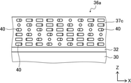
- FIG. 1 conceptually shows an example of an optically anisotropic layer of the liquid crystal diffractive element of the present invention.
- the optically anisotropic layer is formed by using a liquid crystal composition containing a liquid crystal compound, and the direction of the optical axis derived from the liquid crystal compound is at least one direction in the plane. Towards, it has a liquid crystal orientation pattern that is continuously converting.
- the optically anisotropic layer is a cross-sectional image obtained by observing a cross section cut in the thickness direction along a direction in which the direction of the optical axis continuously changes with a scanning electron microscope (SEM).
- SEM scanning electron microscope
- the optically anisotropic layer has a region in which the inclination direction of the dark portion (bright portion) is different in the thickness direction.
- the bright and dark areas (bright and dark lines) in the image of the cross section observed by SEM are observed derived from the liquid crystal phase having a liquid crystal orientation pattern.
- the optically anisotropic layer 36a shown in FIG. 1 uses a rod-shaped liquid crystal compound as the liquid crystal compound 40. Therefore, the direction of the optical axis coincides with the longitudinal direction of the liquid crystal compound 40.
- the optically anisotropic layer 36 has a predetermined liquid crystal orientation pattern in which the optical axis derived from the liquid crystal compound 40 changes while continuously rotating in one direction. Further, the optically anisotropic layer 36a has one cycle in the liquid crystal alignment pattern when the length in which the direction of the optical axis derived from the liquid crystal compound 40 rotates 180 ° in the plane in one direction is set as one cycle. The length is constant.
- the optically anisotropic layer 36a having such a liquid crystal alignment pattern is a liquid crystal display that transmits incident light by diffracting (refracting) it in one cycle in which the optical axis rotates 180 ° and according to the wavelength of the incident light. Acts as a diffractive element.
- the action of the optically anisotropic layer 36a as a diffractive element will be described in detail later.
- the optically anisotropic layer 36a is derived from the liquid crystal phase and extends from one surface to the other in a cross-sectional image obtained by SEM observing a cross section cut in the thickness direction along one direction in which the optical axis rotates.
- a striped pattern having alternating bright and dark portions 42 is observed.
- the bright portion 42 and the dark portion 44 are shown superimposed on the cross section of the optically anisotropic layer 36a.
- a cross-sectional image obtained by observing a cross-section cut in the thickness direction along one direction in which the optical axis rotates is simply referred to as a “cross-sectional SEM image”.
- the optically anisotropic layer 36a of the illustrated example has two inflection points at which the angle changes in the dark portion 44 in the cross-sectional SEM image. That is, it can be said that the optically anisotropic layer 36a has three regions, a region 37a, a region 37b, and a region 37c, in the thickness direction, depending on the inflection point of the dark portion 44.
- the optical axis derived from the liquid crystal compound 40 rotates clockwise in the in-plane direction at any position in the thickness direction toward the left in the figure. It has a rotating liquid crystal orientation pattern. Further, in the liquid crystal alignment pattern, one cycle, which is the length of rotation of the optical axis by 180 ° in one direction, is constant in any region in the in-plane direction.
- the liquid crystal compound 40 is spirally twisted clockwise (clockwise) from the upper side to the lower side in the figure in the thickness direction in the lower region 37c in the thickness direction. As such, it is twisted and oriented.
- the liquid crystal compound 40 is not twisted in the thickness direction, and the liquid crystal compounds 40 stacked in the thickness direction have their optical axes oriented in the same direction. That is, the liquid crystal compounds 40 existing at the same position in the in-plane direction have their optical axes oriented in the same direction.
- the liquid crystal compound 40 is twisted and oriented so as to be spirally twisted counterclockwise (counterclockwise) from the upper side to the lower side in the figure in the thickness direction. That is, in the optically anisotropic layer 36a shown in FIG. 1, the region 37a, the region 37b, and the region 37c are different from each other in the twisted state of the liquid crystal compound 40 in the thickness direction.
- the bright portion 42 and the dark portion 44 in the cross-sectional SEM image of the optically anisotropic layer 36a are the same. Observed to tie the oriented liquid crystal compound 40.
- FIG. 1 shows that the dark portion 44 is observed so as to connect the liquid crystal compounds 40 whose optical axes are oriented in the direction orthogonal to the paper surface.
- the dark portion 44 is inclined toward the upper left in the figure.
- the dark portion 44 extends in the thickness direction.
- the dark portion 44 is inclined toward the upper right in the figure. That is, the optically anisotropic layer 36a shown in FIG. 1 has two angle inflection points at which the angle of the dark portion 44 changes. Further, in the uppermost region 37a, the dark portion 44 is inclined toward the upper right, and in the lowermost region 37b, the dark portion 44 is inclined toward the upper left. That is, the inclination direction of the dark portion 44 is different between the region 37a and the region 37c.
- the dark portion 44 has one inflection point where the inclination direction is folded back in the opposite direction.
- the dark portion 44 of the optically anisotropic layer 36a has an inclined direction in the region 37a and an inclined direction in the region 37b opposite to each other. Therefore, the inflection point located at the interface between the region 37a and the region 37b is the inflection point where the inclination direction is folded back in the opposite direction. That is, the optically anisotropic layer 36a has one inflection point in which the inclination direction is folded back in the opposite direction.
- the regions 37a and the regions 37c have, for example, the same thickness, and as described above, the twisted states of the liquid crystal compound 40 in the thickness direction are different from each other. Therefore, as shown in FIG. 1, the bright portion 42 and the dark portion 44 in the cross-sectional SEM image are substantially C-shaped. Therefore, in the optically anisotropic layer 36a, the shape of the dark portion 44 (bright portion 42) is symmetrical with respect to the center line in the thickness direction.
- the liquid crystal diffractive element of the present invention has such an optically anisotropic layer 36a, that is, a bright portion 42 and a dark portion 44 extending from one surface to the other surface in a cross-sectional SEM image, and the dark portion 44 has a dark portion 44.
- an optically anisotropic layer 36a that is, a bright portion 42 and a dark portion 44 extending from one surface to the other surface in a cross-sectional SEM image
- the dark portion 44 has a dark portion 44.
- a liquid crystal diffractive element having an optically anisotropic layer having a liquid crystal alignment pattern in which the orientation of the optical axis derived from the liquid crystal compound rotates continuously in at least one direction is described in, for example, the entire visible light range. Over a wide wavelength range, incident light can be diffracted at different diffraction angles depending on the wavelength.
- the conventional liquid crystal diffractometer having a liquid crystal orientation pattern has an inflection in which the angle changes in the cross-sectional SEM image, although it has a dark portion inclined with respect to the surface (main surface). It has no points, or as shown in Patent Document 1, it has only one inflection point. Therefore, the conventional liquid crystal diffractive element has a large wavelength dependence of the diffraction efficiency, for example, the diffraction efficiency of red light and green light is high, but the diffraction efficiency of blue light is lower than that of the other two colors.
- the dark portion 44 observed in the cross-sectional SEM image has two or more angle inflection points, and the inclination direction is different in the thickness direction.
- the liquid crystal diffractive element of the present invention has a small wavelength dependence of diffraction efficiency and can diffract light with the same diffraction efficiency regardless of the wavelength.
- such a liquid crystal diffractive element of the present invention can diffract light with high diffraction efficiency regardless of the wavelength.
- the liquid crystal alignment pattern of the liquid crystal diffractive element of the present invention may have a constant length of one cycle in which the optical axis is rotated by 180 °.
- the liquid crystal diffractive element of the present invention diffracts (refracts) light at the same angle if the wavelength is the same, regardless of the incident position of the light in the plane. Therefore, in the liquid crystal diffractive element of the present invention, light of the same wavelength diffracts light at the same angle regardless of the incident position, such as an optical incident element to a light guide plate in AR glass and a spectroscopic element in a hyperspectral camera. It can be suitably used for various optical devices that require the above. The same applies to the liquid crystal diffractive element of the present invention having the optically anisotropic layer shown below with respect to such an action and effect.
- the optically anisotropic layer 36a shown in FIG. 1 has three regions in the thickness direction, the dark portion 44 has two inflection points, and one inflection point in which the inflection direction is folded back. Have a place.
- the optically anisotropic layer is not limited to this configuration. That is, in the liquid crystal diffraction element of the present invention, the optically anisotropic layer has the above-mentioned liquid crystal alignment pattern, one cycle of the liquid crystal alignment pattern is constant, and further, in the cross-sectional SEM image, due to the liquid crystal layer.
- It has a bright portion 42 and a dark portion 44 extending from one surface to the other surface, and the dark portion 44 has two or more angle variation points, and further, in the thickness direction, in the inclination direction.
- Various configurations are available as long as they have different regions.
- FIG. 2 shows another example of the optically anisotropic layer of the liquid crystal diffractive element of the present invention.
- the optically anisotropic layer 36b shown in FIG. 2 also has a predetermined liquid crystal orientation pattern in which the optical axis derived from the liquid crystal compound changes while continuously rotating in one direction. Therefore, in the cross-sectional SEM image, the optically anisotropic layer 36b also has a striped pattern derived from the liquid crystal layer and alternately having bright portions 42 and dark portions 44 extending from one surface to the other surface. .. Similar to FIG. 1, FIG. 2 also shows the bright portion 42 and the dark portion 44 superimposed on the cross section of the optically anisotropic layer 36a.
- the dark portion 44 observed in the cross-sectional SEM image has three inflection points at which the angle changes. That is, it can be said that the optically anisotropic layer 36b has four regions, a region 37d, a region 37e, a region 37f, and a region 37g, from the top in the thickness direction, depending on the inflection point of the dark portion 44. ..
- the optically anisotropic layer 36b of FIG. 2 is also a liquid crystal display in which the optical axis derived from the liquid crystal compound 40 rotates clockwise in the in-plane direction at any position in the thickness direction toward the left in the figure. It has an orientation pattern. Further, in the liquid crystal alignment pattern, one cycle, which is the length of rotation of the optical axis by 180 ° in one direction, is constant in any region in the in-plane direction.
- the liquid crystal compound 40 in the optically anisotropic layer 36b shown in FIG. 2, in the lowermost region 37g in the thickness direction, the liquid crystal compound 40 is spirally twisted clockwise from the upper side to the lower side in the figure in the thickness direction. It is twisted and oriented. In the second region 37f from the bottom, the liquid crystal compound 40 is twisted and oriented so as to be spirally twisted counterclockwise from the upper side to the lower side in the figure in the thickness direction. In the third region 37e from the bottom, the liquid crystal compound 40 is twisted and oriented so as to be spirally twisted clockwise from the upper side to the lower side in the figure in the thickness direction.
- the liquid crystal compound 40 is twisted and oriented so as to be spirally twisted counterclockwise from the upper side to the lower side in the figure in the thickness direction. That is, in the optically anisotropic layer 36b shown in FIG. 2, the liquid crystal orientation pattern is uniform over the entire area in the thickness direction, but the state of the spiral twist in the thickness direction of the liquid crystal compound 40 is the region 37d and the region 37f. Is the same, and the region 37e and the region 37g are the same. Further, in the optically anisotropic layer 36b shown in FIG. 2, the state of the spiral twist in the thickness direction of the liquid crystal compound 40 is opposite in the region 37d and the region 37e.
- the dark portion 44 is observed to tie the liquid crystal compounds 40 in the same orientation. Therefore, in the optically anisotropic layer 36b shown in FIG. 2, the inclination directions of the dark portion 44 of the region 37d and the region 37f are the same, and the inclination directions of the dark portion 44 of the region 37e and the region 37g are the same. Specifically, in the lowermost region 37g in the thickness direction, the dark portion 44 is inclined toward the upper left in the figure.
- the dark portion 44 is inclined toward the upper right in the figure.
- the dark portion 44 is inclined toward the upper left in the figure, like the bottom region 37g.
- the dark portion 44 is inclined toward the upper right in the figure, similarly to the second region 37f from the bottom. That is, the optically anisotropic layer 36b shown in FIG. 2 has three inflection points of the angle of the dark portion where the angle of the dark portion 44 changes.
- the inclination direction of the dark portion is different between the region 37g and the region 37f, which are regions adjacent to each other in the thickness direction. Further, the inclination direction of the dark portion is different between the region 37f and the region 37e, which are regions adjacent to each other in the thickness direction. Further, the inclination direction of the dark portion is different between the region 37e and the region 37d, which are regions adjacent to each other in the thickness direction. That is, in the optically anisotropic layer 36d shown in FIG. 2, the dark portion 44 has three inflection points at which the angle of the dark portion changes, all of which are inflection points in which the inclination direction is folded back.
- the area 37d and the area 37g, and the area 37e and the area 37f have the same thickness as an example. Therefore, in the optically anisotropic layer 36b shown in FIG. 2, the bright portion 42 and the dark portion 44 in the cross-sectional SEM image are substantially W-shaped. Therefore, the shape of the dark portion 44 of the optically anisotropic layer 36b is also symmetrical with respect to the center line in the thickness direction.
- the configuration of the optically anisotropic layer has the above-mentioned liquid crystal alignment pattern in addition to the above-mentioned example, and one cycle of the liquid crystal alignment pattern is constant, and further, a cross-sectional SEM image. Due to the liquid crystal phase observed in, it has a bright portion 42 and a dark portion 44 extending from one surface (main surface) to the other surface, and the dark portion 44 has two or more angular variation points.
- Various configurations can be used as long as they have regions having different inclination directions in the thickness direction.
- each region of the optically anisotropic layer has the above-mentioned liquid crystal orientation in which the optical axis continuously rotates in one direction. Has a pattern. Further, in the liquid crystal alignment pattern, one cycle in which the optical axis derived from the liquid crystal compound rotates by 180 ° is constant.
- the liquid crystal compound 40 is twist-oriented in the thickness direction in the region where the dark portion 44 is inclined with respect to the surface (main surface) of the optically anisotropic layer.
- the main surface is the maximum surface of a sheet-like material (plate-like material, film, layer).
- an optically anisotropic layer having four regions in the thickness direction is exemplified according to the inflection point of the dark portion 44 as conceptually shown in FIG.
- the dark portion 44 in the lowermost region, the dark portion 44 is inclined toward the upper left in the figure. In the second region from the bottom, the dark portion 44 tilts toward the upper left in the figure at a larger angle with respect to the surface than the lowest region. In the third region from the bottom, the dark portion 44 is inclined toward the upper right in the figure. Further, in the uppermost region, the dark portion 44 is inclined toward the upper right in the figure at a smaller angle with respect to the surface than the third region from the bottom.
- the optically anisotropic layer shown in FIG. 3 has three inflection points at which the angle of the dark portion 44 changes, and the inflection points at which the inclination direction of the dark portion is folded back are the second from the bottom. It has one place at the interface between the region and the third region from the bottom.
- the bottom region and the top region, and the second region from the bottom and the third region from the bottom have the same thickness.
- the angles (absolute values of angles) formed by the surface of the optically anisotropic layer and the dark portion 44 are the same.
- the second region from the bottom and the third region from the bottom have different inclination directions, but the angles formed by the surface of the optically anisotropic layer and the dark portion 44 are the same. That is, in the optically anisotropic layer shown in FIG. 3, the bright portion 42 and the dark portion 44 in the cross-sectional SEM image are substantially C-shaped. Therefore, also in the optically anisotropic layer shown in FIG. 3, the shape of the dark portion 44 is symmetrical with respect to the center line in the thickness direction.
- the angle of the dark portion 44 with respect to the surface of the optically anisotropic layer is the length of one cycle, which is the length of rotation of the optical axis by 180 ° toward one direction in the plane, which will be described later, and the thickness direction. It can be adjusted by the magnitude of the twist of the liquid crystal compound 40 that is twist-oriented.
- an optically anisotropic layer having five regions in the thickness direction is exemplified according to the inflection point of the dark portion 44 conceptually shown in FIG.
- the dark portion 44 in the lowermost region, the dark portion 44 is inclined toward the upper left in the figure.
- the dark portion 44 tilts toward the upper left in the figure at a larger angle with respect to the surface than the lowest region.
- the dark portion 44 In the third region from the bottom, that is, the central region in the thickness direction, the dark portion 44 extends in the thickness direction of the optically anisotropic layer.
- the dark portion 44 is inclined toward the upper right in the figure. Further, in the uppermost region, the dark portion 44 is inclined toward the upper right in the figure at a smaller angle with respect to the surface than the fourth region from the bottom.
- the optically anisotropic layer shown in FIG. 4 has four inflection points at which the angle of the dark portion 44 changes. Further, the inclination direction of the dark portion 44 is opposite between the bottom region and the second region from the bottom, the fourth region from the bottom, and the top region. Therefore, the inflection point located at the interface between the second region from the bottom and the fourth region from the bottom is an inflection point in which the inclination direction is folded in the opposite direction. That is, the optically anisotropic layer shown in FIG. 3 has one inflection point in which the inclination direction is folded back in the opposite direction.
- the bottom region and the top region, and the second region from the bottom and the second region from the top have the same thickness.
- the lowermost region and the uppermost region have different inclination directions, but the angle formed by the surface of the optically anisotropic layer and the dark portion 44 is the same.
- the second region from the bottom and the fourth region from the bottom have different inclination directions, but the angles formed by the surface of the optically anisotropic layer and the dark portion 44 are the same.
- the dark portion 44 extends in the thickness direction of the optically anisotropic layer. That is, in the optically anisotropic layer shown in FIG.
- the bright portion 42 and the dark portion 44 in the cross-sectional SEM image are substantially C-shaped. Therefore, also in the optically anisotropic layer shown in FIG. 4, the shape of the dark portion 44 is symmetrical with respect to the center line in the thickness direction.
- the optically anisotropic layer of the liquid crystal diffractive element of the present invention has a thickness as conceptually shown in FIG. 5 by exemplifying a configuration having a substantially C-shaped dark portion 44 shown in FIGS. 3 and 4. By shortening the spacing between the regions in the direction, that is, the spacing between the inflection points in the thickness direction, it is possible to configure the dark portion 44 to continuously change.
- the number of inflection points of the dark portion 44 of the optically anisotropic layer is not limited, and may be two or more. Further, there is no limit to the number of inflection points at which the inclination direction of the dark portion 44 is folded back. However, as shown in FIGS. 1 to 5, the number of inflection points in which the inclination direction is folded is preferably an odd number in that the shape of the dark portion 44 can be made symmetrical with respect to the center line in the thickness direction. 5 or 3 locations are more preferred. Further, the number of inflection points at which the inclination direction is folded back can be preferably 5 or more.
- the shape of the dark portion 44 is symmetrical with respect to the center line in the thickness direction.
- the shape of the dark portion 44 in the optically anisotropic layer does not have to be symmetrical with respect to the center line in the thickness direction.
- the optically anisotropic layer conceptually shown in FIG. 6 is exemplified.
- the optically anisotropic layer shown in FIG. 6 has three regions depending on the inflection point of the dark portion 44.
- the dark portion 44 in the lowermost region, the dark portion 44 is inclined toward the upper left in the figure.
- the dark portion 44 tilts toward the upper left in the figure at a larger angle with respect to the surface than the lowest region.
- the dark portion 44 in the uppermost region, the dark portion 44 is inclined toward the upper right in the figure. That is, in the optically anisotropic layer shown in FIG. 6, the dark portion 44 has three inflection points. Further, at the interface between the second region from the bottom and the uppermost region, there is one inflection point at which the inclination direction of the dark portion 44 is folded back.
- the inclination angles of the dark portion 44 with respect to the surface of the optically anisotropic layer are all different in the three regions, and although there are differences in the inclination direction, the surface of the optically anisotropic layer is gradually increased from the bottom to the top.
- the angle with respect to (absolute value of the angle) becomes large. That is, in the optically anisotropic layer shown in FIG. 6, the shape of the dark portion 44 is asymmetric with respect to the center line in the thickness direction.
- the configuration in which the shape of the dark portion 44 shown in FIGS. 1 to 5 described above is symmetrical with respect to the center line in the thickness direction is advantageous in that the wavelength dependence of the diffraction efficiency is smaller.
- the shape of the dark portion 44 is asymmetrical with respect to the center line in the thickness direction, and in particular, as shown in FIG. 6, the inclination angle is sequentially set with respect to the surface of the optically anisotropic layer.
- the larger configuration is advantageous in that the diffraction efficiency can be increased even when the diffraction angle (refraction angle) is large.
- the tilt angle of the dark portion 44 is an absolute value of the tilt angle.
- the average inclination angle of the dark portion 44 is an angle formed by a line connecting a contact point with one surface of the dark portion 44 and a contact point with the other surface with a perpendicular line on the surface of the optically anisotropic layer. Is. Therefore, when the shape of the dark portion 44 is targeted at the center line in the thickness direction as shown in FIGS. 1 to 5, the average inclination angle of the dark portion 44 is approximately 0 °.
- a rod-shaped liquid crystal compound is used as the liquid crystal compound, but the present invention is not limited to this, and a disk-shaped liquid crystal compound can also be used.
- the optical axis derived from the liquid crystal compound is defined as an axis perpendicular to the disk surface, a so-called phase-advancing axis.
- the optically anisotropic layer may be used in combination with a rod-shaped liquid crystal compound and a disk-shaped liquid crystal compound, as conceptually shown in FIG.
- the rod-shaped liquid crystal compound and the disk-shaped liquid crystal compound By combining the rod-shaped liquid crystal compound and the disk-shaped liquid crystal compound, it is possible to diffract light with high diffraction efficiency with respect to light incident at different angles.
- the combination of the rod-shaped liquid crystal compound and the disk-shaped liquid crystal compound is not limited to the configuration conceptually shown in FIG. 7, and can be used in various configurations.
- the rod-shaped liquid crystal compound may be a combination of the rod-shaped liquid crystal compound and the disk-shaped liquid crystal compound.
- the rod-shaped liquid crystal compound and the disk-shaped liquid crystal compound may be further subdivided and laminated in the thickness direction.
- the liquid crystal diffractive element of the present invention having such a liquid crystal alignment pattern and an optically anisotropic layer having a dark portion 44 (bright portion 42) includes, for example, a support, an alignment film formed on the surface of the support, and an alignment film. It has an optically anisotropic layer formed on the surface of the alignment film.
- FIG. 9 shows an enlarged conceptual diagram of a minute region of the liquid crystal diffraction element including the optically anisotropic layer 36a (region 37c). Note that FIG. 8 is a plan view of the optically anisotropic layer 36a shown in FIG. As described above, the liquid crystal diffraction element shown in FIG. 9 has a support 30, an alignment film 32, and an optically anisotropic layer 36a.
- the liquid crystal diffractive element of the present invention is not limited to this, and various layer configurations can be used.
- the liquid crystal diffractive element of the present invention may be composed of an alignment film 32 and an optically anisotropic layer 36a from which the support 30 is peeled off from the liquid crystal diffractive element shown in FIG.
- the liquid crystal diffractive element of the present invention may be composed of only the optically anisotropic layer 36a from which the support 30 and the alignment film 32 are peeled off from the liquid crystal diffractive element shown in FIG.
- the liquid crystal diffraction element of the present invention may be composed of the support 30 and the optically anisotropic layer 36a.
- the liquid crystal diffractive element of the present invention may have other layers such as a protective layer (hard coat layer) and an antireflection layer in addition to these configurations.
- the liquid crystal diffraction element of the present invention is It comprises an optically anisotropic layer formed by using a liquid crystal composition containing a liquid crystal compound.
- the optically anisotropic layer has a liquid crystal orientation pattern in which the orientation of the optical axis derived from the liquid crystal compound changes while continuously rotating along at least one direction in the plane.
- the length of the optical axis derived from the liquid crystal compound rotated by 180 ° in the plane is set as one cycle, the length of one cycle in the liquid crystal alignment pattern gradually changes along one direction.
- the optically anisotropic layer has a bright part and a dark part extending from one surface to the other surface in a cross-sectional image obtained by observing a cross section cut in the thickness direction along one direction with a scanning electron microscope.
- the dark part has inflection points of two or more angles, It may be a liquid crystal diffractive element having a region in which the inclination direction of the dark portion is different in the thickness direction.
- the liquid crystal orientation pattern of the liquid crystal layer 36 goes from the inside to the outside in one direction (arrows A 1 to A 3 ) in which the direction of the optical axis of the liquid crystal compound 40 changes while continuously rotating. It is a concentric pattern having concentric circles.
- the concentric pattern is a pattern in which the lines connecting the liquid crystal compounds whose optical axes are oriented in the same direction are circular, and the circular line segments are concentric.
- one direction in which the direction of the optical axis of the liquid crystal compound 40 changes while continuously rotating is provided radially from the center of the liquid crystal layer 36. It is a liquid crystal alignment pattern.
- the optical axis of the liquid crystal compound 40 (not shown) is the longitudinal direction of the liquid crystal compound 40.
- the orientation of the optical axis of the liquid crystal compound 40 is a number of directions outward from the center of the optically anisotropic layer 36a, for example, the direction indicated by the arrow A 1 and the direction indicated by the arrow A 2 . It changes while continuously rotating along the direction indicated by the arrow A3 .
- Arrow A 1 , arrow A 2 , and arrow A 3 are array axes described later.
- the optically anisotropic layer 36a of the liquid crystal diffractive element has a region in which one cycle ⁇ of the liquid crystal alignment pattern is different in the plane.
- one cycle ⁇ of the liquid crystal alignment pattern is the length of the liquid crystal alignment pattern in which the optical axis of the liquid crystal compound 40 rotates 180 ° in one direction in which the direction of the optical axis continuously rotates and changes in the plane. It is (distance).
- one cycle ⁇ is directed from the center to the outside.
- the gradual change of one cycle ⁇ means that the one cycle ⁇ changes continuously and that the one cycle ⁇ changes stepwise.
- the diffraction angle by the liquid crystal diffractive element depends on the one cycle ⁇ of the liquid crystal alignment pattern, and the smaller the one cycle ⁇ , the larger the diffraction angle.
- the optically anisotropic layer 36a is provided in one direction in which the liquid crystal alignment pattern changes while the direction of the optical axis of the liquid crystal compound 40 continuously rotates, radially from the center of the optically anisotropic layer 36a, and in each direction.
- the circular polarization incident on the optically anisotropic layer 36a having this liquid crystal alignment pattern is the optics of the liquid crystal compound 40.
- Each is bent (diffused) in individual local regions with different axial orientations. At this time, each diffraction angle differs depending on one cycle in the region where the circular polarization is incident.
- the optically anisotropic layer 36a having a concentric liquid crystal alignment pattern that is, a liquid crystal alignment pattern in which the optical axis continuously rotates and changes radially, is the rotation direction of the optical axis of the liquid crystal compound 40 and the incident circular polarization. Depending on the direction, the incident light can be transmitted as focused light. That is, by making the liquid crystal alignment pattern of the optically anisotropic layer 36a concentric, the liquid crystal diffraction element 10a exhibits a function as, for example, a convex lens.
- the optically anisotropic layer 36a has a bright portion 42 and a dark portion 44 extending from one surface to the other surface in the SEM image, and the dark portion 44. However, it has an inflection point of two or more angles, and has a region in which the inclination direction of the dark portion 44 is different in the thickness direction.
- the optically anisotropic layer 36a has a striped pattern of a bright portion 42 and a dark portion 44, and one dark portion 44 has a change in inclination angle with respect to a surface at two points in the thickness direction, respectively. is doing. That is, each dark portion 44 has two inflection points. Further, in any of the dark portions 44, the inclination direction in the upper region in the figure and the inclination direction in the lower region in the figure are opposite to each other. That is, each dark portion 44 has a region having a different inclination direction.
- the liquid crystal diffractive element shown in FIG. 9 has a support 30, it is not necessary to provide the support 30.
- the optical element of the present invention comprises the optical element of the present invention by peeling off the support 30 from the above configuration and using only the alignment film and the liquid crystal layer, or by peeling off the alignment film and using only the liquid crystal layer. You may.
- liquid crystal diffusing element various layer configurations can be used as long as the liquid crystal layer has a liquid crystal orientation pattern in which the direction of the optical axis derived from the liquid crystal compound rotates in one direction.
- the dark portion 44 observed in the cross-sectional SEM image has two or more angle inflection points, and the region in which the inclination direction is different in the thickness direction.
- the liquid crystal diffractive element of the present invention has a small wavelength dependence of diffraction efficiency and can diffract light with the same diffraction efficiency regardless of the wavelength.
- such a liquid crystal diffractive element of the present invention can diffract light with high diffraction efficiency regardless of the wavelength.
- the length of one cycle in which the optical axis rotates by 180 ° may change in the plane.
- the liquid crystal diffracting element of the present invention diffracts (refracts) light having the same wavelength at different angles depending on the incident position of the light in the plane. Therefore, the liquid crystal diffractive element of the present invention can emit light of the same wavelength at different angles regardless of the incident position, such as a lens element in a head-mounted display for VR and a lens element that improves color cracking when combined with a refraction lens. It can also be suitably used for various optical devices that are required to be diffracted by.
- the support 30 supports the alignment film 32 and the optically anisotropic layer 36a.
- various sheet-like materials films, plate-like materials
- a transparent support is preferable, and a polyacrylic resin film such as polymethylmethacrylate, a cellulose resin film such as cellulose triacetate, and a cycloolefin polymer film (for example, trade name "Arton", manufactured by JSR Corporation).
- a polyacrylic resin film such as polymethylmethacrylate
- a cellulose resin film such as cellulose triacetate
- a cycloolefin polymer film for example, trade name "Arton", manufactured by JSR Corporation.
- trade name "Zeonoa” manufactured by Nippon Zeon Co., Ltd.
- PET polyethylene terephthalate
- polycarbonate polycarbonate
- polyvinyl chloride polyvinyl chloride
- the support is not limited to the flexible film, but may be a non-flexible substrate such as a glass substrate. Further, the support 30 may be multi-layered. Examples of the multilayer support include those including any of the above-mentioned supports as a substrate and having another layer provided on the surface of the substrate.
- the thickness of the support 30 is not limited, and the thickness capable of holding the alignment film and the optically anisotropic layer may be appropriately set according to the application of the liquid crystal diffractive element, the forming material of the support 30, and the like. good.
- the thickness of the support 30 is preferably 1 to 1000 ⁇ m, more preferably 3 to 250 ⁇ m, still more preferably 5 to 150 ⁇ m.
- Alignment film An alignment film 32 is formed on the surface of the support 30.
- the alignment film 32 is an alignment film for orienting the liquid crystal compound 40 in the above-mentioned predetermined liquid crystal alignment pattern when forming the optically anisotropic layer 36a.
- the direction of the optical axis 40A (see FIG. 8) derived from the liquid crystal compound 40 is one direction in the plane (direction of arrow X described later). It has a liquid crystal orientation pattern that changes while rotating continuously along it. Therefore, the alignment film is formed so that the optically anisotropic layer can form this liquid crystal alignment pattern. Further, in the liquid crystal alignment pattern, the length in which the direction of the optical axis 30A rotates by 180 ° in one direction in which the direction of the optical axis 30A changes while continuously rotating is defined as one cycle ⁇ (rotation cycle of the optical axis). ..
- the direction of the optic axis 40A rotates is also simply referred to as “the optical axis 40A rotates”.
- a rubbing-treated film made of an organic compound such as a polymer an oblique vapor deposition film of an inorganic compound, a film having a microgroove, and Langmuir of an organic compound such as ⁇ -tricosanoic acid, dioctadecylmethylammonium chloride and methyl stearylate.
- an organic compound such as ⁇ -tricosanoic acid, dioctadecylmethylammonium chloride and methyl stearylate.
- Examples thereof include a membrane obtained by accumulating LB (Langmuir-Blodgett) membranes produced by the Brodget method.
- the alignment film by the rubbing treatment can be formed by rubbing the surface of the polymer layer with paper or cloth several times in a certain direction.
- Materials used for the alignment film include polyimide, polyvinyl alcohol, polymers having a polymerizable group described in JP-A-9-152509, JP-A-2005-97377, JP-A-2005-99228, and JP-A-2005-99228.
- the materials used for forming the alignment film and the like described in JP-A-2005-128503 are preferably exemplified.
- a so-called photo-alignment film which is obtained by irradiating a photo-alignable material with polarized or non-polarized materials to form an alignment film, is preferably used as the alignment film. That is, in the liquid crystal diffractive element of the present invention, as the alignment film, a photoalignment film formed by applying a photoalignment material on the support 30 is preferably used. Polarized irradiation can be performed from a vertical direction or an oblique direction with respect to the photoalignment film, and non-polarized irradiation can be performed from an oblique direction with respect to the photoalignment film.
- Examples of the photo-alignment material used for the photo-alignment film that can be used in the present invention include JP-A-2006-285197, JP-A-2007-76839, JP-A-2007-138138, and JP-A-2007-94071. JP-A-2007-121721, JP-A-2007-140465, JP-A-2007-156439, JP-A-2007-133184, JP-A-2009-109831, Patent No. 3883848 and Patent No.
- Photodimrizable compounds described in Japanese Patent Application Laid-Open No. 2013-177561 and Japanese Patent Application Laid-Open No. 2014-12823, particularly cinnamate compounds, chalcone compounds, coumarin compounds and the like are exemplified as preferable examples.
- azo compounds, photocrosslinkable polyimides, photocrosslinkable polyamides, photocrosslinkable esters, cinnamate compounds, and chalcone compounds are preferably used.
- the thickness of the alignment film is not limited, and the thickness at which the required alignment function can be obtained may be appropriately set according to the material for forming the alignment film.
- the thickness of the alignment film is preferably 0.01 to 5 ⁇ m, more preferably 0.05 to 2 ⁇ m.
- the method for forming the alignment film there is no limitation on the method for forming the alignment film, and various known methods depending on the material for forming the alignment film can be used. As an example, a method of applying an alignment film to the surface of the support 30 and drying the alignment film and then exposing the alignment film with a laser beam to form an alignment pattern is exemplified.
- FIG. 10 conceptually shows an example of an exposure apparatus that exposes an alignment film to form the above-mentioned alignment pattern.
- the exposure apparatus 60 shown in FIG. 10 uses a light source 64 provided with a laser 62, a ⁇ / 2 plate 65 for changing the polarization direction of the laser beam M emitted by the laser 62, and a laser beam M emitted from the laser 62 as a beam MA and a beam M. It includes a beam splitter 68 that separates the MB into two, mirrors 70A and 70B arranged on the optical paths of the two separated rays MA and MB, respectively, and ⁇ / 4 plates 72A and 72B. Although not shown, the light source 64 emits linearly polarized light P 0 .
- the ⁇ / 4 plate 72A converts the linearly polarized light P 0 (ray MA) into the right circularly polarized light PR, and the ⁇ / 4 plate 72B converts the linearly polarized light P 0 (ray MB) into the left circularly polarized light PL.
- a support 30 having an alignment film 32 before the alignment pattern is formed is arranged in the exposed portion, and two light rays MA and light rays MB are crossed and interfered with each other on the alignment film 32, and the interference light is made to interfere with the alignment film 32. Is exposed to light. Due to the interference at this time, the polarization state of the light applied to the alignment film 32 periodically changes in the form of interference fringes. As a result, in the alignment film 32, an alignment pattern in which the alignment state changes periodically can be obtained. That is, an alignment film having an alignment pattern in which the alignment state changes periodically (hereinafter, also referred to as a pattern alignment film) can be obtained.
- the period of the orientation pattern can be adjusted by changing the intersection angle ⁇ of the two rays MA and MB. That is, in the exposure apparatus 60, in an orientation pattern in which the optical axis 40A derived from the liquid crystal compound 40 continuously rotates along one direction by adjusting the crossing angle ⁇ , the optical axis 40A rotates in one direction. , The length of one cycle (one cycle ⁇ ) in which the optical axis 40A rotates 180 ° can be adjusted.
- the optical axis 40A derived from the liquid crystal compound 40 is unidirectionally oriented as described later.
- optically anisotropic layer 36a having a liquid crystal alignment pattern that rotates continuously toward the surface. Further, the rotation direction of the optical shaft 40A can be reversed by rotating the optical axes of the ⁇ / 4 plates 72A and 72B by 90 °, respectively.
- the orientation of the optical axis derived from the liquid crystal compound in the optically anisotropic layer formed on the pattern alignment film is continuously rotated along at least one direction in the plane. It has an alignment pattern that orients the liquid crystal compound 40 so as to have a changing liquid crystal alignment pattern.
- the pattern alignment film has an axis along the direction in which the liquid crystal compound 40 is oriented as the alignment axis
- the pattern alignment film changes while the orientation of the alignment axis continuously rotates along at least one direction in the plane. It can be said that it has an orientation pattern.
- the alignment axis of the pattern alignment film can be detected by measuring the absorption anisotropy. For example, when the pattern alignment film is irradiated while rotating linearly polarized light and the amount of light transmitted through the pattern alignment film is measured, the direction in which the amount of light is maximum or minimum is gradually along one direction in the plane. It changes and is observed.
- the alignment film is provided as a preferred embodiment and is not an essential constituent requirement.
- the optically anisotropic layer 36a or the like becomes a liquid crystal compound 40. It is also possible to have a liquid crystal alignment pattern in which the orientation of the derived optical axis 40A changes while continuously rotating along at least one direction in the plane.
- the exposure device for the alignment film 32 is not limited to the example shown in FIG. FIG. 14 shows another example of an exposure apparatus that exposes the alignment film 32.
- the exposure apparatus shown in FIG. 14 is an example of an exposure apparatus that forms a concentric alignment pattern as shown in FIG. 13 on an alignment film.
- the exposure apparatus 80 includes a light source 84 provided with a laser 82, a polarization beam splitter 86 that splits the laser beam M from the laser 82 into an S-polarized MS and a P-polarized MP, and a mirror 90A arranged in the optical path of the P-polarized MP. It also has a mirror 90B arranged in the optical path of the S-polarized MS, a lens 92 arranged in the optical path of the S-polarized MS, a polarizing beam splitter 94, and a ⁇ / 4 plate 96.
- the P-polarized MP divided by the polarizing beam splitter 86 is reflected by the mirror 90A and incident on the polarizing beam splitter 94.
- the S-polarized MS divided by the polarizing beam splitter 86 is reflected by the mirror 90B, condensed by the lens 92, and incident on the polarized beam splitter 94.
- the P-polarized MP and the S-polarized MS are combined by a polarizing beam splitter 94 and become right-handed circularly polarized light and left-handed circularly polarized light according to the polarization direction by the ⁇ / 4 plate 96, and the alignment film 32 on the support 30 is formed. Incident to.
- the polarization state of the light applied to the alignment film changes periodically in the form of interference fringes. Since the intersection angle of the left circular polarization and the right circular polarization changes from the inside to the outside of the concentric circles, an exposure pattern in which the pitch changes from the inside to the outside can be obtained. As a result, in the alignment film, a concentric alignment pattern in which the alignment state changes periodically can be obtained.
- one cycle ⁇ of the liquid crystal alignment pattern in which the optical axis of the liquid crystal compound 40 continuously rotates 180 ° along one direction is the focal length of the lens 92 (F number of the lens 92) and the focal length of the lens 92. It can be controlled by changing the distance, the distance between the lens 92 and the alignment film 32, and the like. Further, by adjusting the refractive power of the lens 92 (F number of the lens 92), the length ⁇ of one cycle of the liquid crystal alignment pattern can be changed in one direction in which the optical axis rotates continuously.
- the length ⁇ of one cycle of the liquid crystal alignment pattern can be changed in one direction in which the optical axis continuously rotates by the spreading angle of the light spread by the lens 92 that interferes with the parallel light. More specifically, when the refractive power of the lens 92 is weakened, it approaches parallel light, so that the length ⁇ of one cycle of the liquid crystal alignment pattern gradually shortens from the inside to the outside, and the F number becomes large. On the contrary, when the refractive power of the lens 92 is increased, the length ⁇ of one cycle of the liquid crystal alignment pattern suddenly shortens from the inside to the outside, and the F number becomes small.
- one cycle ⁇ is not gradually changed toward the array axis D direction, but partially in the array axis D direction.
- a configuration in which one cycle ⁇ has different regions is also available.
- a method of partially changing one cycle ⁇ a method of scanning and exposing a photoalignment film while arbitrarily changing the polarization direction of the focused laser light and patterning can be used.
- the wavelength of the laser used for exposing the alignment film can be appropriately set according to the type of the alignment film to be used and the like.
- a laser having a wavelength of deep ultraviolet to visible light to infrared can be preferably used.
- a laser having a wavelength of 266 nm, 325 nm, 355 nm, 370 nm, 385 nm, 405 nm, and 460 nm can be used, but the above is not limited to the above, and various wavelengths are used depending on the type of alignment film and the like.
- a laser can be used.
- the optically anisotropic layer may be peeled off and transferred from the alignment film.
- the transfer can be performed a plurality of times depending on the bonded surface of the optically anisotropic layer.
- the peeling / transfer method can be freely selected according to the purpose. For example, after transferring once to a substrate having an adhesive layer, it is retransferred to an object to be transferred, and the substrate is peeled off to obtain optical light.
- the interface of the anisotropic layer on the alignment film side can be set to the object side to be transferred.
- the optically anisotropic layer opposite to the alignment film is on the side of the object to be transferred, the optically anisotropic layer and the object to be transferred are bonded together via an adhesive, and then the alignment film is used.
- the optically anisotropic layer may be peeled off from the above.
- the alignment film may be used repeatedly as long as there is no problem in orientation. Before the optically anisotropic layer is provided on the alignment film, the alignment film can be washed with an organic solvent or the like.
- Optically anisotropic layer An optically anisotropic layer 36a is formed on the surface of the alignment film 32.
- the optically anisotropic layer 36a contains only the liquid crystal compound 40 (liquid crystal compound molecule) on the surface of the alignment film. Shows.
- the optically anisotropic layer 36a is an optically anisotropic layer formed by using a composition containing a normal liquid crystal compound, as conceptually shown by exemplifying the optically anisotropic layer 36a in FIG. Similarly, it has a structure in which the oriented liquid crystal compounds 40 are stacked.
- the optically anisotropic layer 36a has three regions, a region 37c, a region 37b, and a region 37a, depending on the inflection point of the dark portion 44, from the bottom. Only the bottom (support 30 side) region 37c is shown for the sake of brevity.
- the optically anisotropic layer 36a is formed by using a composition containing a liquid crystal compound.
- the optically anisotropic layer functions as a general ⁇ / 2 plate, that is, is orthogonal to each other contained in the light incident on the optically anisotropic layer. It has a function of giving a phase difference of half a wavelength, that is, 180 ° to two linearly polarized light components.
- the incident circular polarization is refracted (diffracted) in the direction in which the direction of the optical axis is continuously rotating. And transparent.
- the direction of diffraction differs depending on the turning direction of the incident circularly polarized light. That is, the optically anisotropic layer transmits circularly polarized light and diffracts the transmitted light. Further, the optically anisotropic layer changes the swirling direction of the transmitted circularly polarized light in the opposite direction.
- the direction of the optical axis derived from the liquid crystal compound continuously rotates in one direction indicated by the arrow D (hereinafter, also referred to as the arrangement axis D) in the plane of the optically anisotropic layer. It has a changing liquid crystal orientation pattern.
- the direction of the array axis D is the X direction
- the direction orthogonal to the direction of the array axis D is the Y direction.
- the optical axis 40A derived from the liquid crystal compound 40 is a so-called slow-phase axis having the highest refractive index in the liquid crystal compound 40.
- the optical axis 40A is along the long axis direction of the rod shape.
- the optical axis 40A derived from the liquid crystal compound 40 is also referred to as "optical axis 40A of liquid crystal compound 40" or "optical axis 40A".
- the liquid crystal compounds 40 are two-dimensionally oriented in the plane parallel to the arrow X direction and the Y direction orthogonal to the arrow X direction in the optically anisotropic layer 36a, respectively. There is. In FIGS. 1 to 6, the Y direction is the direction perpendicular to the paper surface.
- FIG. 8 conceptually shows a plan view of the optically anisotropic layer 36a.
- it is a view of the optically anisotropic layer 36a viewed from a direction orthogonal to the surface.
- the liquid crystal compound 40 shows only the liquid crystal compound 40 on the surface of the alignment film 32.
- the optically anisotropic layer 36a has a structure in which the liquid crystal compound 40 is stacked from the liquid crystal compound 40 on the surface of the alignment film 32 in the thickness direction, as shown in FIG.
- optically anisotropic layer 36a in the plane is described as a representative example in FIG. 8, basically the same configuration and operation and effect are described at each position in the plane of the optically anisotropic layer. Has.
- the optically anisotropic layer 36a has a liquid crystal alignment pattern in which the orientation of the optical axis 40A changes while continuously rotating along the arrangement axis D direction in the plane of the optically anisotropic layer 36a.
- the fact that the direction of the optic axis 40A changes while continuously rotating in the array axis D direction (predetermined one direction) is specifically that the liquid crystal compound 40 arranged along the array axis D direction is changed.
- the angle formed by the optical axis 40A and the array axis D direction differs depending on the position in the array axis D direction, and the angle formed by the optical axis 40A and the array axis D direction along the array axis D direction is ⁇ to ⁇ + 180.
- the difference in the angles of the optical axes 40A of the liquid crystal compounds 40 adjacent to each other in the arrangement axis D direction is preferably 45 ° or less, more preferably 15 ° or less, and further preferably a smaller angle. preferable.
- the liquid crystal compound 40 forming the optically anisotropic layer 36a has the orientation of the optical axis 40A in the Y direction orthogonal to the D direction of the arrangement axis, that is, the Y direction orthogonal to one direction in which the optical axis 40A continuously rotates.
- the liquid crystal compounds 40 having the same optics are arranged at equal intervals.
- the angles formed by the direction of the optical axis 40A and the direction of the arrangement axis D are equal between the liquid crystal compounds 40 arranged in the Y direction.
- the optical axis 40A rotates 180 ° in the arrangement axis D direction in which the direction of the optical axis 40A continuously rotates and changes in the plane.
- the length (distance) to be performed be the length ⁇ of one cycle in the liquid crystal alignment pattern.
- the length of one cycle in the liquid crystal alignment pattern is defined by the distance from ⁇ to ⁇ + 180 ° between the optical axis 40A and the arrangement axis D direction.
- the length of one cycle in the liquid crystal alignment pattern is the length of one cycle in the periodic structure of the diffractive element.
- the distance between the centers of the two liquid crystal compounds 40 having the same angle with respect to the array axis D direction in the array axis D direction is defined as the length ⁇ of one cycle.
- the distance between the centers of the two liquid crystal compounds 40 in which the direction of the arrangement axis D and the direction of the optical axis 40A coincide with each other in the direction of the arrangement axis D is the length ⁇ of one cycle.
- this length ⁇ of one cycle is also referred to as "one cycle ⁇ ".
- the liquid crystal alignment pattern of the optically anisotropic layer repeats this one cycle ⁇ in the direction of the arrangement axis D, that is, in one direction in which the direction of the optical axis 40A continuously rotates and changes.
- the liquid crystal compounds arranged in the Y direction have the same angle formed by the optical axis 40A and the arrangement axis D direction (one direction in which the direction of the optical axis of the liquid crystal compound 40 rotates). ..
- the region in which the liquid crystal compound 40 having the same angle formed by the optical axis 40A and the arrangement axis D direction is arranged in the Y direction is defined as a region R.
- the value of the in-plane retardation (Re) in each region R is preferably half wavelength, that is, ⁇ / 2.
- the difference in the refractive index due to the refractive index anisotropy of the region R in the optically anisotropic layer is the refractive index in the direction of the slow axis in the plane of the region R and the direction orthogonal to the direction of the slow axis. It is a refractive index difference defined by the difference from the refractive index of.
- the refractive index difference ⁇ n due to the refractive index anisotropy of the region R is the refractive index of the liquid crystal compound 40 in the direction of the optical axis 40A and the liquid crystal compound 40 in the plane of the region R in the direction perpendicular to the optical axis 40A. Equal to the difference from the refractive index. That is, the refractive index difference ⁇ n is equal to the refractive index difference of the liquid crystal compound.
- the optically anisotropic layer 36a When circularly polarized light is incident on such an optically anisotropic layer 36a, the light is diffracted (refracted) and the direction of circularly polarized light is changed.
- This effect is conceptually shown in FIGS. 11 and 12 by exemplifying the optically anisotropic layer 36a.
- the optically anisotropic layer 36a contains only the liquid crystal compound 40 (liquid crystal compound molecule) on the surface of the alignment film. Shows.
- the value of the product of the difference in the refractive index of the liquid crystal compound and the thickness of the optically anisotropic layer is ⁇ / 2.
- the left circle is formed on the optically anisotropic layer 36a.
- the incident light L 1 which is polarized light
- the incident light L 1 is given a phase difference of 180 ° by passing through the optically anisotropic layer 36a, and the transmitted light L 2 is converted into right circular polarization.
- the liquid crystal alignment pattern formed on the optically anisotropic layer 36a is a periodic pattern in the arrangement axis D direction
- the transmitted light L 2 travels in a direction different from the traveling direction of the incident light L 1 . .. In this way, the incident light L 1 with left circular polarization is converted into transmitted light L 2 with right circular polarization tilted by a certain angle in the direction of the array axis D with respect to the incident direction.
- the optically anisotropic layer 36a is formed.
- the incident light L 4 of right circular refraction is incident, the incident light L 4 passes through the optically anisotropic layer 36a and is given a phase difference of 180 °, and is converted into transmitted light L 5 of left circular polarization. Will be done.
- the transmitted light L 5 travels in a direction different from the traveling direction of the incident light L 4 . .. At this time, the transmitted light L 5 travels in a direction different from that of the transmitted light L 2 , that is, in a direction opposite to the direction of the array axis D with respect to the incident direction. In this way, the incident light L 4 is converted into the transmitted light L 5 of left circularly polarized light tilted by a certain angle in the direction opposite to the direction of the array axis D with respect to the incident direction.
- the optically anisotropic layer 36a can adjust the angle of diffraction (refraction) of the transmitted lights L 2 and L 5 by changing one cycle ⁇ of the formed liquid crystal alignment pattern. Specifically, in the optically anisotropic layer 36a, the shorter one cycle ⁇ of the liquid crystal alignment pattern, the stronger the interference between the lights that have passed through the liquid crystal compounds 40 adjacent to each other, so that the transmitted lights L 2 and L 5 are increased. Can be diffracted. Further, by making the rotation direction of the optical axis 40A of the liquid crystal compound 40, which rotates along the arrangement axis D, the opposite direction, the diffraction direction of the transmitted light can be made in the opposite direction. That is, in the examples shown in FIGS. 11 to 12, the rotation direction of the optical axis 40A toward the arrangement axis D direction is clockwise, but by making this rotation direction counterclockwise, the direction of diffraction of transmitted light can be changed. , Can be done in the opposite direction.
- the angle of diffraction (refraction angle) by the optically anisotropic layer 36a differs depending on the wavelength of the incident light. Specifically, the longer the wavelength of light, the greater the diffraction. That is, in the case of red light, green light and blue light, the red light is diffracted most, the green light is diffracted next, and the diffracted blue light is the smallest.
- the one cycle ⁇ in the liquid crystal alignment pattern of the optically anisotropic layer 36a is uniform. Therefore, light of the same wavelength is diffracted at the same angle.
- the angle of the dark portion 44 with respect to the surface of the optically anisotropic layer is the length of one cycle, which is the length at which the optical axis of the liquid crystal compound rotates 180 ° toward one direction in the plane, and the thickness. It can be adjusted by the magnitude of the twist of the liquid crystal compound 40 twist-oriented in the isotropic direction.
- the shorter the period ⁇ and the smaller the twist in the thickness direction the larger the angle of the dark portion 44 with respect to the surface of the optically anisotropic layer. That is, the shorter one cycle and the smaller the twist in the thickness direction, the more the dark portion 44 stands up with respect to the surface of the optically anisotropic layer.
- the shorter one cycle ⁇ of the liquid crystal alignment pattern the larger the diffraction angle of the incident light.
- the tilting direction of the dark portion 44 for example, the tilting direction toward the upper right in the figure and the tilting direction toward the upper left in the figure are the rotation directions (clockwise or counterclockwise) of the optical shaft 40A toward one direction in the plane. It can be selected depending on the twist direction (clockwise or counterclockwise) in the thickness direction of the liquid crystal compound 40 (clockwise).
- ⁇ n 550 is the refractive index difference due to the refractive index anisotropy of the region R when the wavelength of the incident light is 550 nm
- d is the thickness of the optically anisotropic layer 36a.
- the in-plane retardation Re (550) ⁇ n 550 ⁇ d is more preferably 225 nm ⁇ ⁇ n 550 ⁇ d ⁇ 340 nm, and even more preferably 250 nm ⁇ ⁇ n 550 ⁇ d ⁇ 330 nm.
- the in-plane retardation values of the plurality of regions R in the optically anisotropic layer 36a can be used outside the range of the above formula (1). Specifically, by setting ⁇ n 550 ⁇ d ⁇ 200 nm or 350 nm ⁇ n 550 ⁇ d, the light traveling in the same direction as the traveling direction of the incident light and the light traveling in a direction different from the traveling direction of the incident light. It can be divided into light. When ⁇ n 550 ⁇ d approaches 0 nm or 550 nm, the component of light traveling in the same direction as the traveling direction of the incident light increases, and the component of light traveling in a direction different from the traveling direction of the incident light decreases.
- ⁇ n 450 is the difference in refractive index due to the refractive index anisotropy of the region R when the wavelength of the incident light is 450 nm.
- the formula (2) represents that the liquid crystal compound 40 contained in the optically anisotropic layer 36a has reverse dispersibility. That is, by satisfying the equation (2), the optically anisotropic layer 36a can cope with incident light having a wavelength in a wide band.
- the optically anisotropic layer is composed of a cured layer of a liquid crystal composition containing a rod-shaped liquid crystal compound or a disk-shaped liquid crystal compound, and the optical axis of the rod-shaped liquid crystal compound or the optical axis of the disk-shaped liquid crystal compound is a liquid crystal oriented as described above. It has an orientation pattern.
- the optically anisotropic layer is formed by forming an alignment film 32 having the above-mentioned alignment pattern on the support 30, and applying and curing the liquid crystal composition on the alignment film. Further, the structure of the optically anisotropic layer in which the optical axis of the liquid crystal compound is spirally twisted and rotated in the thickness direction of the optically anisotropic layer is such that the liquid crystal compound is spirally oriented in the thickness direction of the liquid crystal composition. It can be formed by adding a chiral agent to be added.
- optically anisotropic layer in which the dark portion 44 has two or more inflection points and the dark portion 44 has a region in which the inclination direction of the dark portion 44 is different in the thickness direction, each region in the thickness direction is formed.
- optically anisotropic layers having different configurations may be formed.
- the optically anisotropic layer 36a shown in FIG. 1 when forming the optically anisotropic layer 36a shown in FIG. 1, first, a chiral agent that induces a right-handed twist in the thickness direction on an alignment film 32 having an alignment pattern formed on the support 30.
- the liquid crystal composition containing the above is applied, and the liquid crystal compound 40 is spirally oriented in the thickness direction by heating or the like, and then the liquid crystal composition is cured to form a region 37c.
- the alignment pattern formed on the alignment film 32 is an alignment pattern in which the optical axis 40A derived from the liquid crystal compound 40 continuously rotates in one direction (array axis D) in the plane.
- the optical axis 40A derived from the liquid crystal compound 40 continuously rotates in one direction in the in-plane direction, and in the thickness direction, from top to bottom in the thickness direction.
- the liquid crystal compound 40 is in a state of being twisted and oriented in the clockwise direction.
- a liquid crystal composition similar to that of the region 37c is applied onto the formed region 37c except that the chiral agent is not contained, and the liquid crystal composition is cured to form the region 37b.
- the orientation pattern of the liquid crystal compound in the plane follows the orientation pattern of the lower liquid crystal layer. Therefore, in the region 37b, as in the region 37c, the optical axis 40A derived from the liquid crystal compound 40 continuously rotates in one direction, and the region 37b is not twisted or oriented in the thickness direction. In addition, the directions of the optical axes 40A of the liquid crystal compound 40 are aligned.
- a liquid crystal composition similar to that of the region 37c is applied onto the formed region 37b except that a chiral agent that induces a left twist in the thickness direction is used, and the liquid crystal compound 40 is twisted and oriented in the thickness direction by heating or the like. After that, the liquid crystal composition is cured to form the region 37a.
- the liquid crystal layer by the coating method follows the orientation pattern of the lower layer. Therefore, in the region 37a, the optical axis 40A continuously rotates in one direction in the in-plane direction as in the region 37b and the like, and in the thickness direction, from top to bottom in the thickness direction. The liquid crystal compound 40 is in a state of being twisted and oriented in the counterclockwise direction. As a result, as shown in FIG.
- the optically anisotropic layer 36a having the above can be formed.
- the magnitude of the torsional orientation of the liquid crystal compound twisted and oriented in the thickness direction can be adjusted by the type of the chiral agent added to the liquid crystal composition and the amount of the chiral agent added. Further, the twisting direction (right twist / left twist) of the liquid crystal compound in the thickness direction can also be selected by selecting the type of chiral agent to be added to the liquid crystal composition.
- the optically anisotropic layer of the present invention is an example in which the optical axis derived from the liquid crystal compound is not inclined with respect to the interface of the optically anisotropic layer at the interface of the optically anisotropic layer.
- the optical axis derived from the liquid crystal compound may be inclined.
- the optical axis derived from the liquid crystal compound may have a pretilt angle with respect to the interface of the optically anisotropic layer.
- the optic axis derived from the liquid crystal compound changes its inclination angle in the thickness direction from one interface of the optically anisotropic layer toward the other interface. It is also good.
- the phase difference of the optically anisotropic layer can be adjusted, and appropriately adjusted so as to obtain high diffraction efficiency. be able to.
- the film thickness of the optically anisotropic layer may change in the plane.
- a liquid crystal diffractive element in which the length of one cycle in the liquid crystal alignment pattern changes in the plane high diffraction efficiency is obtained for light having different incident positions by changing the film thickness of the optically anisotropic layer in the plane. Can be adjusted as appropriate to obtain.
- the region 37a, the region 37b, and the region 37c of the optically anisotropic layer shown in the example of FIG. 1 are the central portion.
- the thickness of each region may be the same or different.
- the thickness of each region of the optically anisotropic layer may be the same in the plane or may be changed. The thickness of each region of the optically anisotropic layer can be appropriately set according to the desired performance.
- the present invention includes an embodiment in which a laminated body integrally provided with a support and an alignment film functions as a ⁇ / 2 plate.
- the liquid crystal composition for forming the optically anisotropic layer contains a rod-shaped liquid crystal compound or a disk-shaped liquid crystal compound, and further contains other components such as a leveling agent, an orientation control agent, a polymerization initiator and an orientation aid. May be contained.
- the thickness of the optically anisotropic layer is not limited, and the desired optical characteristics can be obtained according to one cycle ⁇ of the liquid crystal alignment pattern, the required diffraction angle, the diffraction efficiency, and the like.
- the thickness may be set as appropriate.
- the thickness of each region corresponding to the inflection point of the dark portion 44 may or may not be uniform, and may be appropriately set according to the required diffraction angle and the like.
- rod-shaped liquid crystal compound examples include azomethines, azoxys, cyanobiphenyls, cyanophenyl esters, benzoic acid esters, cyclohexanecarboxylic acid phenyl esters, cyanophenylcyclohexanes, cyano-substituted phenylpyrimidines, and alkoxy-substituted phenylpyrimidines.
- Phenyldioxans, trans and alkenylcyclohexylbenzonitriles are preferably used. Not only small molecule liquid crystal molecules as described above, but also high molecular weight liquid crystal molecules can be used.
- the disk-shaped liquid crystal compound for example, those described in JP-A-2007-108732 and JP-A-2010-244033 can be preferably used.
- the liquid crystal compound 40 rises in the thickness direction in the optically anisotropic layer, and the optical shaft 40A derived from the liquid crystal compound is a disk surface. It is defined as an axis perpendicular to the so-called phase advance axis.
- a liquid crystal compound having a high refractive index anisotropy ⁇ n can be preferably used in order to obtain high diffraction efficiency.
- the liquid crystal compound having a high refractive index anisotropy ⁇ n is not particularly limited, but the compound exemplified in WO2019 / 182129 A1 and the compound represented by the following general formula (I) can be preferably used.
- P 1 and P 2 independently represent a hydrogen atom, -CN, -NCS or a polymerizable group.
- Sp 1 and Sp 2 independently represent a single bond or a divalent linking group, respectively.
- Sp 1 and Sp 2 do not represent a divalent linking group containing at least one group selected from the group consisting of aromatic hydrocarbon ring groups, aromatic heterocyclic groups and aliphatic hydrocarbon ring groups. ..
- R represents a hydrogen atom or an alkyl group having 1 to 10 carbon atoms.
- Rs When there are a plurality of Rs, they may be the same or different.
- Z 1 and Z 2 they may be the same or different.
- a plurality of Z 3s may be the same or different.
- Z 3 linked to Sp 2 represents a single bond.
- X 1 and X 2 independently represent a single bond or S-, respectively.
- a plurality of X 1 and X 2 may be the same or different from each other. However, at least one of the plurality of X 1 and the plurality of X 2 represents -S-.
- k represents an integer of 2 to 4.
- m and n each independently represent an integer of 0 to 3.
- a plurality of m may be the same or different.
- a 1 , A 2 , A 3 and A 4 are independently represented by any of the following general formulas (B-1) to (B-7), or the following general formulas (B-1) to A4. Represents a group formed by connecting two or more and three or less groups represented by any one of (B-7).
- a plurality of A 2 and A 3 may be the same or different from each other. When there are a plurality of A 1 and A 4 , they may be the same or different.
- W 1 to W 18 independently represent CR 1 or N, and R 1 represents a hydrogen atom or the following substituent L.
- R 1 represents a hydrogen atom or the following substituent L.
- Y 1 to Y 6 independently represent NR 2 , O or S, respectively, and R 2 represents a hydrogen atom or the following substituent L.
- G 1 to G 4 independently represent CR 3 R 4 , NR 5 , O or S, and R 3 to R 5 independently represent a hydrogen atom or the following substituent L, respectively.
- M 1 and M 2 independently represent CR 6 or N, respectively, and R 6 represents a hydrogen atom or the following substituent L. * Represents the bond position.
- the substituent L is an alkyl group having 1 to 10 carbon atoms, an alkoxy group having 1 to 10 carbon atoms, an alkylamino group having 1 to 10 carbon atoms, an alkylthio group having 1 to 10 carbon atoms, and 1 carbon atom number.
- alkanoyl groups alkanoyloxy groups with 1 to 10 carbon atoms, alkanoylamino groups with 1 to 10 carbon atoms, alkanoylthio groups with 1 to 10 carbon atoms, alkyloxycarbonyl groups with 2 to 10 carbon atoms , Alkylaminocarbonyl group with 2 to 10 carbon atoms, alkylthiocarbonyl group with 2 to 10 carbon atoms, hydroxy group, amino group, mercapto group, carboxy group, sulfo group, amide group, cyano group, nitro group, halogen atom Or it is a polymerizable group.
- the above-mentioned group described as the substituent L has -CH 2-
- a group substituted with C- is also included in the substituent L.
- the group described as the substituent L has a hydrogen atom
- at least one of the hydrogen atoms contained in the group is replaced with at least one selected from the group consisting of a fluorine atom and a polymerizable group.
- the group is also included in the substituent L.
- the refractive index anisotropy ⁇ n 550 of the liquid crystal compound is preferably 0.15 or more, more preferably 0.2 or more, further preferably 0.25 or more, and 0. .3 or more is the most preferable.
- the refractive index anisotropy ⁇ n and the average refractive index of the optically anisotropic layer may be changed in the plane.
- the chiral agent has a function of inducing a spiral structure in which the liquid crystal compound is twisted and oriented in the thickness direction.
- the chiral agent may be selected according to the purpose because the twisting direction and / or the degree of twisting (spiral pitch) of the induced spiral differs depending on the compound.
- the chiral agent is not particularly limited, and is a chiral agent for known compounds (for example, Liquid Crystal Device Handbook, Chapter 3, Section 4-3, TN (Twisted Nematic), STN (Super Twisted Nematic), p. 199, Japan Science Promotion.
- isosorbide a chiral agent having an isosorbide structure
- isomannide derivative an isomannide derivative
- the chiral agent a chiral agent that causes return isomerization, dimerization, isomerization, dimerization, etc. by irradiation with light and whose spiral-inducing force (HTP: Helical Twisting Power) is lowered is also preferably used. It is possible.
- the chiral agent generally contains an asymmetric carbon atom, but an axial asymmetric compound or a plane asymmetric compound containing no asymmetric carbon atom can also be used as the chiral agent.
- Examples of axial or asymmetric compounds include binaphthyl, helicene, paracyclophane, and derivatives thereof.
- the chiral agent may have a polymerizable group. When both the chiral agent and the liquid crystal compound have a polymerizable group, the repeating unit derived from the polymerizable liquid crystal compound and the repeating unit derived from the chiral agent are derived by the polymerization reaction between the polymerizable chiral agent and the polymerizable liquid crystal compound. Polymers with repeating units can be formed.
- the polymerizable group of the polymerizable chiral agent is preferably a group of the same type as the polymerizable group of the polymerizable liquid crystal compound. Therefore, the polymerizable group of the chiral agent is preferably an unsaturated polymerizable group, an epoxy group or an aziridinyl group, more preferably an unsaturated polymerizable group, and preferably an ethylenically unsaturated polymerizable group. More preferred. Moreover, the chiral agent may be a liquid crystal compound.
- the chiral agent has a photoisomerizing group
- a pattern of a desired reflection wavelength corresponding to the emission wavelength can be formed by irradiation with a photomask such as an active ray after coating and orientation.
- a photomask such as an active ray after coating and orientation.
- an isomerization site of a compound exhibiting photochromic properties, an azo group, an azoxy group, or a cinnamoyl group is preferable.
- Specific compounds include JP-A-2002-08478, JP-A-2002-08851, JP-A-2002-179668, JP-A-2002-179669, JP-A-2002-179670, and JP-A-2002.
- the content of the chiral agent in the liquid crystal composition may be appropriately set according to the amount of the desired spiral twist in the thickness direction and the type of the chiral agent.
- the dark portion 44 observed in the cross-sectional SEM image has two or more angle inflection points, and has a region in which the inclination direction is different in the thickness direction. .. Therefore, the liquid crystal diffractive element of the present invention has a small wavelength dependence of diffraction efficiency and can diffract light with the same diffraction efficiency regardless of the wavelength.
- red light, green light, and blue light can be diffracted with the same diffraction efficiency.
- light can be diffracted with high diffraction efficiency regardless of the wavelength, and the higher the diffraction efficiency, the lower the wavelength dependence of the diffraction efficiency.
- one cycle ⁇ in which the optical axis derived from the liquid crystal compound rotates by 180 ° is constant. Therefore, regardless of the incident position of the light in the plane, if the wavelength is the same, the light is diffracted (refracted) at the same angle. That is, for example, in the case of red light, the light can be diffracted at the same angle regardless of the position of incidence on the liquid crystal diffractive element.
- the optically anisotropic layer has a concentric circle shape from the inside to the outside in which the direction of the optical axis derived from the liquid crystal compound changes while continuously rotating.
- the configuration has the liquid crystal orientation pattern of, but is not limited to this.
- the arrangement axis D of the liquid crystal alignment pattern of the optically anisotropic layer may be provided in one direction, and one cycle ⁇ may be gradually changed along this one direction.
- the liquid crystal alignment pattern may be an asymmetric liquid crystal alignment pattern instead of a concentric circle symmetrical from the inside to the outside. At that time, the center of the liquid crystal alignment pattern may be different from the center of the liquid crystal diffractive element.
- the liquid crystal alignment pattern is not limited to the above configuration, and may be appropriately set according to the function required for the liquid crystal diffractive element.
- Such a liquid crystal diffractive element of the present invention can also be preferably used in combination with a circular polarizing plate.
- a part of the circularly polarized light incident on the liquid crystal diffractive element of the present invention may pass through the liquid crystal diffractive element without being diffracted (0th order light).
- Circular polarization that is not diffracted by the liquid crystal diffractive element may reduce the performance depending on the application.
- by combining the liquid crystal diffractive element and the circular polarizing plate it is possible to reduce the light (0th order light) transmitted without being diffracted by the liquid crystal diffractive element.
- the circular polarizing plate has a retardation plate and a linear polarizing plate, and in the optical element of the present invention, a liquid crystal diffraction element, a retardation plate, and a linear polarizing plate are arranged in this order. It was done.
- the right circular polarization is incident on the liquid crystal diffractive element of the present invention, the incident right circular polarization is diffracted and emitted from the liquid crystal diffractive element. Further, when diffracted, the right circular polarization is converted into the left circular polarization.
- the left circular polarization (that is, primary light) diffracted by the liquid crystal diffractive element is converted into linear polarization by the retardation plate (1/4 wave plate) of the circular polarizing plate.
- the linearly polarized light converted by the retardation plate is transmitted through the linearly polarizing plate and emitted.
- the right circular polarization (that is, 0th-order light) not diffracted by the liquid crystal diffractometer is the position of the circularly polarizing plate. It is converted into linearly polarized light in a direction orthogonal to the left circularly polarized light (primary light) that is incident on the phase difference plate and diffracted, and is incident on the linearly polarizing plate and absorbed. That is, the right circularly polarized light that is not diffracted by the liquid crystal diffractive element is absorbed by the circularly polarizing plate. Therefore, it is possible to transmit the desired primary light due to the left circular polarization and reduce the right circular polarization that has not been diffracted. Therefore, it is possible to suppress deterioration of performance due to unnecessary light (0th order light).
- another optical element may be used in combination downstream of the circularly polarizing plate.
- a retardation plate may be arranged downstream of the circularly polarizing plate.
- the circular polarizing plate has a retardation plate and a linear polarizing plate arranged in this order.
- a depolarization layer that eliminates the polarization state of light in at least a part of the wavelength range may be used.
- the depolarization layer include a high retardation film and a light scattering layer. By controlling the polarization state of the light emitted from the circular polarizing plate in this way, it is possible to adjust the polarization state according to the application.
- the high retardation film is, for example, a film having an in-plane retardation of 3000 nm or more.
- an optical element that deflects light may be arranged downstream of the circular polarizing plate.
- the traveling direction of the light emitted from the circular polarizing plate can be changed.
- the deflection direction of the light emitted from the circular polarizing plate can be adjusted according to the application.
- the linear polarizing plate used in the present invention is not particularly limited as long as it is a linear polarizing plate having a function of transmitting linear polarization in one polarization direction and absorbing linear polarization in the other polarization direction, and is not particularly limited to the conventionally known linear polarizing plate. You can use the board.
- the linear polarizing plate may be an absorption type linear polarizing plate or a reflection type linear polarizing plate.
- an iodine-based polarizing element which is an absorption-type polarizing element, a dye-based polarizing element using a dichroic dye, a polyene-based polarizing element, and the like are used.
- Iodine-based splitters and dye-based splitters include coated and stretched splitters, both of which can be applied.
- a polarizing element produced by adsorbing iodine or a dichroic dye on polyvinyl alcohol and stretching it is preferable.
- the absorption type polarizing element a splitter in which the dichroic dye is oriented by utilizing the orientation of the liquid crystal without stretching is particularly preferable. This polarizing element can be extremely thinned to a thickness of about 0.1 to 5 ⁇ m, cracks are unlikely to occur when bent as described in Japanese Patent Application Laid-Open No. 2019-194685, and thermal deformation is small. As described in Japanese Patent No.
- the dichroic dye oriented polarizing element is used for applications that require high brightness, applications that require small size and light weight, applications for fine optical systems, applications for molding on curved surfaces, and applications. It can be used for flexible parts. It is also possible to peel off the support and transfer the polarizing element for use.
- In-vehicle display optical systems such as head-up displays, optical systems such as AR glasses and VR glasses, LiDAR, face recognition systems, and optical sensors such as polarization imaging incorporate an absorption type polarizing element for the purpose of suppressing stray light. It is also preferable.
- the reflective linear polarizing plate for example, a film in which a layer containing two kinds of polymers is stretched, a wire grid polarizing element, or the like as described in JP-A-2011-053705 can be used. .. From the viewpoint of brightness, a film in which a layer containing a polymer is stretched is preferable.
- Commercially available products are also available as the reflective linear polarizing plate.
- a reflective splitter (trade name: APF) manufactured by 3M
- a wire grid splitter (trade name: WGF) manufactured by Asahi Kasei Corporation, and the like can be preferably used.
- a reflective linear polarizing plate in which a cholesteric liquid crystal film and a ⁇ / 4 plate are combined may be used.
- the polarizing plate used in the present invention preferably has a smooth surface.
- the polarizing plate has an average arithmetic roughness Ra of the surface of 50 nm or less, more preferably 30 nm or less, further preferably 10 nm or less, and further preferably 5 nm or less. Is particularly preferable.
- the height difference of the surface unevenness within the range of 1 square millimeter is preferably 100 nm or less, more preferably 50 nm or less, still more preferably 20 nm or less.
- the surface roughness and the average arithmetic roughness can be measured by using a roughness meter, an interferometer or the like. For example, it can be measured using an interferometer "vertscan" manufactured by Ryoka System Co., Ltd.
- the phase difference plate used in the present invention is a phase difference plate that converts the phase of the incident polarization.
- the retardation plate is arranged by adjusting the direction of the slow axis depending on whether the incident polarization is converted to be closer to linear polarization or to be closer to circular polarization.
- the retardation plate may be arranged so that the slow phase axis is + 45 ° or ⁇ 45 ° with respect to the absorption axis of the linear polarizing plate arranged adjacent to each other.
- the retardation plate used in the present invention may be a single-layer type composed of one optically anisotropic layer, or may be composed of a stack of two or more optically anisotropic layers each having a plurality of different slow phase axes.
- a multi-layer type is also good.
- International Publication No. 2013/137464, International Publication No. 2016/158300, JP-A-2014-209219, JP-A-2014-209220, International Publication No. 2014/157079 , JP-A-2019-215416, and International Publication No. 2019/160044, etc. but are not limited thereto.
- the retardation plate is preferably a ⁇ / 4 plate.
- ⁇ / 4 plate there is no limitation on the ⁇ / 4 plate, and various known plates having a ⁇ / 4 function can be used. Specific examples of the ⁇ / 4 plate include those described in US Patent Application Publication No. 2015/0277006.
- the ⁇ / 4 plate has a single-layer structure
- a stretched polymer film a retardation film in which an optically anisotropic layer having a ⁇ / 4 function is provided on a support, and the like are used.
- the ⁇ / 4 plate has a multi-layer structure
- a wide band ⁇ / 4 plate formed by laminating a ⁇ / 4 plate and a ⁇ / 2 wavelength plate can be specifically mentioned.
- the thickness of the ⁇ / 4 plate is not particularly limited, but is preferably 1 to 500 ⁇ m, more preferably 1 to 50 ⁇ m, and even more preferably 1 to 5 ⁇ m.
- the retardation plate used in the present invention preferably has a reverse wavelength dispersibility. Having the inverse wavelength dispersibility makes the phase change in the phase difference plate ideal, and the conversion between linearly polarized light and circularly polarized light becomes ideal.
- another optical element may be used in combination downstream of the circularly polarizing plate.
- a retardation plate may be arranged downstream of the circularly polarizing plate.
- the linearly polarized light transmitted through the circular polarizing plate (the retardation plate and the linear polarizing plate are arranged in this order) is converted into circularly polarized light, elliptically polarized light, and linearly polarized light having different polarization directions by the retardation plate arranged downstream of the circularly polarizing plate.
- the configuration to be used can also be preferably used.
- a depolarization layer that eliminates the polarization state of light in at least a part of the wavelength range may be used.
- a depolarization layer a high retardation film (in-plane retardation of 3000 nm or more), a light scattering layer, or the like can be used.
- an optical element that deflects light may be arranged downstream of the circular polarizing plate.
- the traveling direction of the light emitted from the circularly polarizing plate can be changed.
- the deflection direction of the light emitted from the circular polarizing plate can be adjusted according to the application.
- the optical film may include an adhesive layer for adhesion of each layer.
- adhesive is used in a concept including “adhesive”.
- water-soluble adhesives UV curable adhesives, emulsion adhesives, latex adhesives, mastic adhesives, multi-layer adhesives, paste adhesives, foam adhesives, supported film adhesives, thermoplastic adhesives.
- Adhesives hot melt adhesives, heat solidified adhesives, thermoactive adhesives, heat seal adhesives, heat curable adhesives, contact adhesives, pressure sensitive adhesives (ie, adhesives), Examples thereof include a polymerizable adhesive, a solvent type adhesive, a solvent active adhesive, and a ceramic adhesive. Specifically, an aqueous solution of a boron compound, a curable adhesive of an epoxy compound containing no aromatic ring in the molecule as shown in JP-A-2004-245925, JP-A-2008-174667, 360 to 450 nm.
- Examples thereof include an active energy ray-curable adhesive containing (meth) acrylic compound and (c) phenolethylene oxide-modified acrylate or nonylphenolethylene oxide-modified acrylate. If necessary, various adhesives may be used alone or in combination.
- the adhesive layer preferably has a small difference in refractive index from the adjacent layer from the viewpoint of reducing unnecessary reflection.
- the difference in refractive index between adjacent layers is preferably 0.05 or less, more preferably 0.01 or less.
- the method for adjusting the refractive index of the adhesive layer is not particularly limited, but a method for adding fine particles such as zirconia-based, silica-based, acrylic-based, acrylic-styrene-based, and melamine-based, adjusting the resin refractive index, and JP-A No. 11
- a known method such as the method described in -223712 can be used.
- the difference in refractive index from the adjacent layers is preferably 0.05 or less in all directions in the in-plane. Therefore, the adhesive layer may have an in-plane refractive index anisotropy.
- the interface reflectance can be reduced by distributing the refractive index in the thickness direction of the adhesive layer.
- a method of distributing the refractive index in the thickness direction a method of providing a plurality of adhesive layers, a method of mixing the interfaces between the adhesive layers provided in the plurality of layers, and a method of controlling the uneven distribution state of the material in the adhesive layer are controlled. Examples include a method of imparting a refractive index distribution.
- the adhesive layer can be provided on one of the members to be bonded or both members by any method such as coating, vapor deposition, transfer, etc., and from the viewpoint of increasing the adhesive strength, after heat treatment and ultraviolet irradiation, etc.
- the treatment can be applied according to the type of adhesive.
- the thickness of the adhesive layer can be adjusted arbitrarily, but is preferably 20 ⁇ m or less, more preferably 0.1 ⁇ m or less. Examples of the method for forming an adhesive layer of 0.1 ⁇ m or less include a method of depositing a ceramic adhesive such as silicon oxide (SiOx layer) on the bonded surface.
- the bonded surface of the bonded member can be subjected to surface modification treatment such as plasma treatment, corona treatment, saponification treatment, etc., and a primer layer can be applied before bonding. Further, when there are a plurality of bonded surfaces, the type and thickness of the adhesive layer can be adjusted for each bonded surface.
- the produced laminate can be cut to a predetermined size.
- the cutting method of the laminated body is not limited, and various known methods such as a method of physically cutting using a blade such as a Thomson blade and a method of cutting by irradiating a laser can be used.
- a laser it is preferable to select the pulse width (nanoseconds, picoseconds, femtoseconds) and wavelength in consideration of cutability and damage to the material.
- the end face may be polished. From the viewpoint of improving workability at the time of cutting and suppressing dust generation, it is possible to cut with a peelable protective film attached.
- the cutting position can be arbitrarily determined.
- the liquid crystal alignment pattern easy to see, it can be observed through a polarizing plate, a retardation film, or the like.
- Marks of any shape can be added as needed for the purpose of installing the laminate on the device with high accuracy, improving the accuracy of the shaft and cutting position at the time of cutting, and the like.
- the type of the mark can be arbitrarily selected, and a method of physically imparting it by a laser, an inkjet method, etc., a method of partially changing the orientation state of the liquid crystal display, or a method of partially decolorizing or dyeing a region is imparted. You can select the method and so on.
- a protective layer gas barrier layer, blocking layer against moisture, ultraviolet absorbing layer, scratch resistant layer, etc.
- the protective layer may be formed directly on the liquid crystal layer, or may be provided via an adhesive layer or another optical film.
- An antireflection layer (LR layer, AR layer, moth-eye layer, etc.) may be provided for the purpose of reducing the reflectance of the surface.
- Various protective layers can be appropriately selected from known ones.
- polyvinyl alcohol is preferable.
- Polyvinyl alcohol can also function as a polarizing element.
- the ultraviolet absorbing layer is a layer containing an ultraviolet absorber, and the ultraviolet absorber has an excellent ability to absorb ultraviolet rays having a wavelength of 370 nm or less, and from the viewpoint of good displayability, visible light having a wavelength of 400 nm or more. Those with low absorption are preferably used.
- ultraviolet absorber Only one type of ultraviolet absorber may be used, or two or more types may be used in combination.
- the ultraviolet absorbers described in JP-A-2001-77282 and JP-A-2002-543265 can be mentioned.
- Specific examples of the ultraviolet absorber include oxybenzophenone compounds, benzotriazole compounds, salicylic acid ester compounds, benzophenone compounds, cyanoacrylate compounds, nickel complex salt compounds and the like.
- the liquid crystal diffractive element of the present invention can be used in combination with a plurality of liquid crystal diffractive elements.
- a plurality of liquid crystal diffractive elements For example, as disclosed in Optics Express, Vol.28, No16 / 3 August 2020, by combining multiple liquid crystal diffractometers and changing the polarization state incident on the liquid crystal diffractometer, the light condensing property of the emitted light is changed. / Multiple divergence can be switched.
- By combining such a plurality of liquid crystal diffractometers it is possible to perform a Foveated display corresponding to the fovea centralis in an HMD such as an AR glass and a VR glass.
- the liquid crystal diffraction element of the present invention can also preferably be configured in combination with a phase modulation element.
- a switchable ⁇ / 2 plate Switchable Half Waveplate
- a liquid crystal diffractive element used as a Passive Element
- the adjustable focal length can be increased to a plurality.
- the liquid crystal diffraction element of the present invention can also preferably be used in combination with other lens elements.
- the liquid crystal diffractive element of the present invention in the combination of the Fresnel lens and the liquid crystal diffractive element as disclosed in SID 2020 DIGEST, 40-4, pp579-582. Therefore, the chromatic aberration of the lens can be improved with high diffraction efficiency.
- refractive index lenses US3,443,858, and pancake lenses as disclosed in Optics Express, Vol.29, No4 / 15 February 2021 and the like. It can be suitably used.
- an optical system that combines such a lens and a liquid crystal diffractive element for AR glasses, VR glasses, and the like, it is possible to improve the color shift (chromatic aberration of the lens) of the display image of the HMD.
- the liquid crystal diffraction element of the present invention can also be preferably used in combination with a light guide plate.
- a light guide plate for example, in a combination of a light guide plate and a lens as disclosed in Proc. Of SPIE Vol.11062, Digital Optical Technologies 2019, 110620J (16 July 2019), by using the liquid crystal diffractive element of the present invention as the above lens, The focal position of the displayed image emitted from the light guide plate can be changed. By combining with the light guide plate in this way, the focal position of the display image of the HMD such as AR glass and VR glass can be adjusted. When used for AR glass, as disclosed in Proc.
- this lens is a lens with different positive and negative positive and negative across the light guide plate.
- the liquid crystal diffractive element of the present invention By using the liquid crystal diffractive element of the present invention, both the actual scene and the display image output from the light guide plate can be observed without distortion.
- the liquid crystal diffraction element of the present invention can also be preferably used in combination with an image display device.
- an image display device as disclosed in Crystals 2021, 11, 107 with a liquid crystal diffractometer (used as a Diffractive Deflection Film)
- the brightness distribution of the emitted light from the image display device can be adjusted. ..
- the brightness distribution of the HMD such as AR glass and VR glass can be suitably adjusted.
- the liquid crystal diffraction element of the present invention can also be preferably used in combination with a light deflection element (beam steering).
- a light deflection element beam steering
- the liquid crystal diffraction element of the present invention as the diffraction element of the light deflection element as disclosed in WO2019 / 189675, it is possible to increase the deflection angle of the emitted light with high diffraction efficiency.
- the light irradiation angle of a distance measuring sensor such as LiDAR (Light Detection and Ranging) can be suitably widened.
- liquid crystal diffusing element the optical element
- the image display unit the head-mounted display
- the beam steering and the sensor of the present invention have been described in detail above, the present invention is not limited to the above examples and does not deviate from the gist of the present invention. Of course, various improvements and changes may be made within the scope.
- the following coating liquid for forming an alignment film was applied onto the support by spin coating.
- the support on which the coating film of the coating film for forming the alignment film was formed was dried on a hot plate at 60 ° C. for 60 seconds to form the alignment film.
- Coating liquid for forming an alignment film ⁇ Material for photo-alignment A 1.00 parts by mass Water 16.00 parts by mass Butoxyethanol 42.00 parts by mass Propylene glycol monomethyl ether 42.00 parts by mass ⁇ ⁇
- the alignment film was exposed using the exposure apparatus shown in FIG. 10 to form an alignment film P-1 having an alignment pattern.
- a laser that emits laser light having a wavelength (325 nm) was used.
- the exposure amount due to the interference light was set to 1000 mJ / cm 2 .
- composition A-1 (Formation of optically anisotropic layer) The following composition A-1 was prepared as a liquid crystal composition forming the first optically anisotropic layer.
- the optically anisotropic layer was formed by coating the composition A-1 on the alignment film P-1 in multiple layers.
- multi-layer coating first, the composition A-1 of the first layer is applied on the alignment film, and after heating, it is cured by ultraviolet rays to prepare a liquid crystal-immobilized layer, and then the second and subsequent layers are applied to the liquid crystal-immobilized layer. It refers to repeating coating by recoating, and similarly heating and then curing with ultraviolet rays.
- the orientation direction of the alignment film is reflected from the lower surface to the upper surface of the optically anisotropic layer even when the total thickness of the optically anisotropic layer is increased.
- the following composition A-1 is applied on the alignment film P-1, the coating film is heated to 80 ° C. on a hot plate, and then the wavelength is increased using a high-pressure mercury lamp under a nitrogen atmosphere.
- the orientation of the liquid crystal compound was fixed by irradiating the coating film with an ultraviolet ray of 365 nm at an irradiation amount of 300 mJ / cm 2 .
- the second and subsequent layers were overcoated on this liquid crystal immobilization layer, heated under the same conditions as above, and then cured by ultraviolet rays to prepare a liquid crystal immobilization layer. In this way, repeated coating was repeated until the total thickness reached a desired film thickness to form an optically anisotropic layer, and a liquid crystal diffractive element was manufactured.
- the complex refractive index ⁇ n of the cured layer of the liquid crystal composition A-1 is applied on a separately prepared support with an alignment film for retardation measurement, and the director of the liquid crystal compound is used as the basis.
- the refractive index value and the film thickness of the liquid crystal immobilization layer (cured layer) obtained by orienting the material so as to be horizontal and then irradiating with ultraviolet rays to immobilize the material were measured and obtained.
- ⁇ n can be calculated by dividing the retardation value by the film thickness. The retardation value was measured at a target wavelength using Axoscan manufactured by Axometrix, and the film thickness was measured using SEM.
- the optically anisotropic layer finally had a liquid crystal display ⁇ n 550 ⁇ thickness (Re (550)) of 275 nm and had a periodic oriented surface.
- ⁇ n 550 ⁇ thickness (Re (550)) 275 nm and had a periodic oriented surface.
- one cycle in which the optical axis of the liquid crystal compound was rotated by 180 ° was 10 ⁇ m.
- the helix angle in the thickness direction of the liquid crystal compound was 70 °.
- measurements such as “ ⁇ n 550 XXd” were performed in the same manner.
- composition A-2 was prepared as a liquid crystal composition forming the second optically anisotropic layer.
- Composition A-2 Liquid crystal compound L-1 100.00 parts by mass Chiral agent H-1 0.32 parts by mass Polymerization initiator (BASF, Irgacure OXE01) 1.00 parts by mass Leveling agent T-1 0.08 parts by mass Methyl ethyl ketone 1050.00 parts by mass ⁇ ⁇
- the second optically anisotropic layer was formed in the same manner as the first optically anisotropic layer except that the film thickness of the optically anisotropic layer was adjusted using the composition A-2.
- the optically anisotropic layer finally had a liquid crystal display ⁇ n 550 ⁇ thickness (Re (550)) of 275 nm and had a periodic oriented surface.
- ⁇ n 550 ⁇ thickness (Re (550)) a liquid crystal display ⁇ n 550 ⁇ thickness (Re (550)) of 275 nm and had a periodic oriented surface.
- Re (550) thickness
- one cycle in which the optical axis of the liquid crystal compound was rotated by 180 ° was 10 ⁇ m.
- the helix angle in the thickness direction of the liquid crystal compound was ⁇ 70 °.
- Example 1 ⁇ Manufacturing of liquid crystal diffraction element> (Formation of alignment film) In the same manner as in Comparative Example 1, an alignment film was formed on the glass substrate, and the alignment film was exposed to form an alignment film P-1 having an alignment pattern.
- composition B-1 (Formation of optically anisotropic layer) The following composition B-1 was prepared as the liquid crystal composition forming the first optically anisotropic layer.
- the first optically anisotropic layer was formed in the same manner as in Comparative Example 1 except that the film thickness of the optically anisotropic layer was adjusted using the composition B-1.
- the optically anisotropic layer finally had a liquid crystal display ⁇ n 550 ⁇ thickness (Re (550)) of 160 nm and had a periodically oriented surface.
- ⁇ n 550 ⁇ thickness (Re (550)) a liquid crystal display ⁇ n 550 ⁇ thickness (Re (550)) of 160 nm and had a periodically oriented surface.
- Re (550) thickness
- one cycle in which the optical axis of the liquid crystal compound was rotated by 180 ° was 10 ⁇ m.
- the helix angle in the thickness direction of the liquid crystal compound was 80 °.
- composition B-2 was prepared as a liquid crystal composition forming the second optically anisotropic layer.
- Composition B-2 ⁇ Liquid crystal compound L-1 100.00 parts by mass Polymerization initiator (BASF, Irgacure OXE01) 1.00 parts by mass Leveling agent T-1 0.08 parts by mass Methyl ethyl ketone 1050.00 parts by mass ⁇ ⁇
- the second optically anisotropic layer was formed in the same manner as the first optically anisotropic layer except that the film thickness of the optically anisotropic layer was adjusted using the composition B-2.
- the optically anisotropic layer finally had a liquid crystal display ⁇ n 550 ⁇ thickness (Re (550)) of 330 nm and had a periodic oriented surface.
- ⁇ n 550 ⁇ thickness (Re (550)) 330 nm and had a periodic oriented surface.
- one cycle in which the optical axis of the liquid crystal compound was rotated by 180 ° was 10 ⁇ m.
- the helix angle in the thickness direction of the liquid crystal compound was 0 °.
- composition B-3 was prepared as the liquid crystal composition forming the third optically anisotropic layer.
- Composition B-3 Liquid crystal compound L-1 100.00 parts by mass Chiral agent H-1 0.63 parts by mass Polymerization initiator (BASF, Irgacure OXE01) 1.00 parts by mass Leveling agent T-1 0.08 parts by mass Methyl ethyl ketone 1050.00 parts by mass ⁇ ⁇
- the third optically anisotropic layer was formed in the same manner as the first optically anisotropic layer except that the film thickness of the optically anisotropic layer was adjusted using the composition B-3.
- the optically anisotropic layer finally had a liquid crystal display ⁇ n 550 ⁇ thickness (Re (550)) of 160 nm and had a periodically oriented surface.
- ⁇ n 550 ⁇ thickness (Re (550)) a liquid crystal display ⁇ n 550 ⁇ thickness (Re (550)) of 160 nm and had a periodically oriented surface.
- Re (550) thickness
- one cycle in which the optical axis of the liquid crystal compound was rotated by 180 ° was 10 ⁇ m.
- the helix angle in the thickness direction of the liquid crystal compound was ⁇ 80 °.
- Example 2 ⁇ Manufacturing of liquid crystal diffraction element> (Formation of alignment film) In the same manner as in Comparative Example 1, an alignment film was formed on the glass substrate, and the alignment film was exposed to form an alignment film P-1 having an alignment pattern.
- the optically anisotropic layer finally had a liquid crystal display ⁇ n 550 ⁇ thickness (Re (550)) of 190 nm and had a periodically oriented surface.
- ⁇ n 550 ⁇ thickness (Re (550)) 190 nm and had a periodically oriented surface.
- one cycle in which the optical axis of the liquid crystal compound was rotated by 180 ° was 10 ⁇ m.
- the helix angle in the thickness direction of the liquid crystal compound was 87 °.
- the chiral agent H-1 was changed to 0.12 parts by mass to prepare the composition C-2.
- the second optically anisotropic layer was formed in the same manner as the third optically anisotropic layer of Example 1 except that the thickness of the optically anisotropic layer was adjusted.
- the optically anisotropic layer finally had a liquid crystal display ⁇ n 550 ⁇ thickness (Re (550)) of 150 nm and had a periodically oriented surface.
- ⁇ n 550 ⁇ thickness (Re (550)) a liquid crystal display ⁇ n 550 ⁇ thickness (Re (550)) of 150 nm and had a periodically oriented surface.
- Re (550) thickness
- one cycle in which the optical axis of the liquid crystal compound was rotated by 180 ° was 10 ⁇ m.
- the helix angle in the thickness direction of the liquid crystal compound was ⁇ 14 °.
- the liquid crystal composition forming the third optically anisotropic layer in the composition B-1 of Example 1, the chiral agent M-1 was changed to 0.07 parts by mass to prepare the composition C-3.
- the third optically anisotropic layer was formed in the same manner as the first optically anisotropic layer of Example 1 except that the thickness of the optically anisotropic layer was adjusted.
- the optically anisotropic layer finally had a liquid crystal display ⁇ n 550 ⁇ thickness (Re (550)) of 150 nm and had a periodically oriented surface.
- ⁇ n 550 ⁇ thickness (Re (550)) a liquid crystal display ⁇ n 550 ⁇ thickness (Re (550)) of 150 nm and had a periodically oriented surface.
- Re (550) thickness
- one cycle in which the optical axis of the liquid crystal compound was rotated by 180 ° was 10 ⁇ m.
- the helix angle in the thickness direction of the liquid crystal compound was 14 °.
- the liquid crystal composition forming the fourth optically anisotropic layer in the composition B-3 of Example 1, the chiral agent H-1 was changed to 0.58 parts by mass to prepare the composition C-4.
- the fourth optically anisotropic layer was formed in the same manner as the third optically anisotropic layer of Example 1 except that the thickness of the optically anisotropic layer was adjusted.
- the optically anisotropic layer finally had a liquid crystal display ⁇ n 550 ⁇ thickness (Re (550)) of 190 nm and had a periodically oriented surface.
- ⁇ n 550 ⁇ thickness (Re (550)) 190 nm and had a periodically oriented surface.
- the liquid crystal alignment pattern of this optically anisotropic layer one cycle in which the optical axis of the liquid crystal compound was rotated by 180 ° was 10 ⁇ m. Further, in this optically anisotropic layer, the helix angle in the thickness direction of the liquid crystal compound was ⁇ 87 °.
- Example 3 ⁇ Manufacturing of liquid crystal diffraction element> (Formation of alignment film) In the same manner as in Comparative Example 1, an alignment film was formed on the glass substrate, and the alignment film was exposed to form an alignment film P-1 having an alignment pattern.
- the optically anisotropic layer finally had a liquid crystal display ⁇ n 550 ⁇ thickness (Re (550)) of 150 nm and had a periodically oriented surface.
- ⁇ n 550 ⁇ thickness (Re (550)) ⁇ n 550 ⁇ thickness
- the chiral agent M-1 was changed to 0.02 parts by mass to prepare the composition D-2.
- the second optically anisotropic layer was formed in the same manner as the first optically anisotropic layer of Example 1 except that the film thickness of the optically anisotropic layer was adjusted.
- the optically anisotropic layer finally had a liquid crystal display ⁇ n 550 ⁇ thickness (Re (550)) of 335 nm and had a periodic oriented surface.
- ⁇ n 550 ⁇ thickness (Re (550)) 335 nm and had a periodic oriented surface.
- one cycle in which the optical axis of the liquid crystal compound was rotated by 180 ° was 10 ⁇ m.
- the helix angle in the thickness direction of the liquid crystal compound was 8 °.
- the liquid crystal composition forming the third optically anisotropic layer in the composition B-3 of Example 1, the chiral agent H-1 was changed to 0.57 parts by mass to prepare the composition D-3.
- the third optically anisotropic layer was formed in the same manner as the third optically anisotropic layer of Example 1 except that the film thickness of the optically anisotropic layer was adjusted.
- the optically anisotropic layer finally had a liquid crystal display ⁇ n 550 ⁇ thickness (Re (550)) of 170 nm and had a periodic oriented surface.
- ⁇ n 550 ⁇ thickness (Re (550)) 170 nm and had a periodic oriented surface.
- Re (550) thickness
- the helix angle of the liquid crystal compound in the thickness direction was ⁇ 78 °.
- the optically anisotropic layer finally had a liquid crystal display ⁇ n 550 ⁇ thickness (Re (550)) of 275 nm and had a periodic oriented surface.
- ⁇ n 550 ⁇ thickness (Re (550)) a liquid crystal display ⁇ n 550 ⁇ thickness (Re (550)) of 275 nm and had a periodic oriented surface.
- Re (550) thickness
- the helix angle in the thickness direction of the liquid crystal compound was 70 °.
- a polarizing microscope shows that the first and second optically anisotropic layers have a liquid crystal display of ⁇ n 550 ⁇ thickness (Re (550)) of 275 nm and a periodic alignment surface. confirmed.
- this optically anisotropic layer one cycle in which the optical axis of the liquid crystal compound was rotated by 180 ° was 1 ⁇ m.
- the helix angle in the thickness direction of the liquid crystal compound is 70 ° in the plane
- the second optically anisotropic layer the helix angle in the thickness direction of the liquid crystal compound is ⁇ 70. There was °.
- the optically anisotropic layer finally had a liquid crystal display ⁇ n 550 ⁇ thickness (Re (550)) of 160 nm and had a periodically oriented surface.
- ⁇ n 550 ⁇ thickness (Re (550)) a liquid crystal display ⁇ n 550 ⁇ thickness (Re (550)) of 160 nm and had a periodically oriented surface.
- Re (550) thickness
- the helix angle in the thickness direction of the liquid crystal compound was 115 °.
- the chiral agent M-1 was changed to 0.16 parts by mass to prepare the composition E-2.
- the second optically anisotropic layer was formed in the same manner as the first optically anisotropic layer of Example 1 except that the film thickness of the optically anisotropic layer was adjusted.
- the optically anisotropic layer finally had a liquid crystal display ⁇ n 550 ⁇ thickness (Re (550)) of 335 nm and had a periodic oriented surface.
- ⁇ n 550 ⁇ thickness (Re (550)) 335 nm and had a periodic oriented surface.
- Re (550) thickness
- the helix angle in the thickness direction of the liquid crystal compound was 76 °.
- the liquid crystal composition forming the third optically anisotropic layer in the composition B-3 of Example 1, the chiral agent H-1 was changed to 0.38 parts by mass to prepare the composition E-3.
- the third optically anisotropic layer was formed in the same manner as the third optically anisotropic layer of Example 1 except that the thickness of the optically anisotropic layer was adjusted.
- the optically anisotropic layer finally had a liquid crystal display ⁇ n 550 ⁇ thickness (Re (550)) of 160 nm and had a periodically oriented surface.
- ⁇ n 550 ⁇ thickness (Re (550)) a liquid crystal display ⁇ n 550 ⁇ thickness (Re (550)) of 160 nm and had a periodically oriented surface.
- Re (550) thickness
- the helix angle in the thickness direction of the liquid crystal compound was ⁇ 48 °.
- the liquid crystal composition forming the first optically anisotropic layer As the liquid crystal composition forming the first optically anisotropic layer, in the composition C-1 of Example 2, the chiral agent M-1 was changed to 0.44 parts by mass to prepare the composition F-1.
- the first optically anisotropic layer was formed in the same manner as the first optically anisotropic layer of Example 2 except that the thickness of the optically anisotropic layer was adjusted.
- the optically anisotropic layer finally had a liquid crystal display ⁇ n 550 ⁇ thickness (Re (550)) of 190 nm and had a periodically oriented surface.
- ⁇ n 550 ⁇ thickness (Re (550)) 190 nm and had a periodically oriented surface.
- Re (550) thickness
- the helix angle in the thickness direction of the liquid crystal compound was 115 °.
- the chiral agent M-1 was changed to 0.09 parts by mass to prepare the composition F-2.
- the second optically anisotropic layer was formed in the same manner as the first optically anisotropic layer of Example 2 except that the thickness of the optically anisotropic layer was adjusted.
- the optically anisotropic layer finally had a liquid crystal display ⁇ n 550 ⁇ thickness (Re (550)) of 150 nm and had a periodically oriented surface.
- ⁇ n 550 ⁇ thickness (Re (550)) a liquid crystal display ⁇ n 550 ⁇ thickness (Re (550)) of 150 nm and had a periodically oriented surface.
- Re (550) thickness
- one cycle in which the optical axis of the liquid crystal compound was rotated by 180 ° was 1 ⁇ m.
- the helix angle in the thickness direction of the liquid crystal compound was 18 °.
- the liquid crystal composition forming the third optically anisotropic layer in the composition C-3 of Example 2, the chiral agent M-1 was changed to 0.04 parts by mass to prepare the composition F-3.
- the third optically anisotropic layer was formed in the same manner as the third optically anisotropic layer of Example 2 except that the thickness of the optically anisotropic layer was adjusted.
- the optically anisotropic layer finally had a liquid crystal display ⁇ n 550 ⁇ thickness (Re (550)) of 150 nm and had a periodically oriented surface.
- ⁇ n 550 ⁇ thickness (Re (550)) ⁇ n 550 ⁇ thickness
- the chiral agent H-1 was changed to 1.99 parts by mass to prepare the composition F-4.
- the fourth optically anisotropic layer was formed in the same manner as the fourth optically anisotropic layer of Example 2 except that the thickness of the optically anisotropic layer was adjusted.
- the optically anisotropic layer finally had a liquid crystal display ⁇ n 550 ⁇ thickness (Re (550)) of 190 nm and had a periodically oriented surface.
- ⁇ n 550 ⁇ thickness (Re (550)) 190 nm and had a periodically oriented surface.
- Re (550) thickness
- one cycle in which the optical axis of the liquid crystal compound was rotated by 180 ° was 1 ⁇ m.
- the helix angle of the liquid crystal compound in the thickness direction was -237 °.
- the liquid crystal composition forming the first optically anisotropic layer As the liquid crystal composition forming the first optically anisotropic layer, in the composition B-1 of Example 1, the chiral agent M-1 was changed to 0.55 parts by mass to prepare the composition F-1.
- the first optically anisotropic layer was formed in the same manner as the first optically anisotropic layer of Example 1 except that the film thickness of the optically anisotropic layer was adjusted.
- the optically anisotropic layer finally had a liquid crystal display ⁇ n 550 ⁇ thickness (Re (550)) of 150 nm and had a periodically oriented surface.
- ⁇ n 550 ⁇ thickness (Re (550)) a liquid crystal display ⁇ n 550 ⁇ thickness (Re (550)) of 150 nm and had a periodically oriented surface.
- Re (550) thickness
- one cycle in which the optical axis of the liquid crystal compound was rotated by 180 ° was 1 ⁇ m.
- the helix angle in the thickness direction of the liquid crystal compound was 114 °.
- the chiral agent M-1 was changed to 0.18 parts by mass to prepare the composition F-2.
- the second optically anisotropic layer was formed in the same manner as the first optically anisotropic layer of Example 1 except that the film thickness of the optically anisotropic layer was adjusted.
- the optically anisotropic layer finally had a liquid crystal display ⁇ n 550 ⁇ thickness (Re (550)) of 335 nm and had a periodic oriented surface.
- ⁇ n 550 ⁇ thickness (Re (550)) 335 nm and had a periodic oriented surface.
- Re (550) thickness
- the helix angle in the thickness direction of the liquid crystal compound was 85 °.
- the liquid crystal composition forming the third optically anisotropic layer in the composition B-3 of Example 1, the chiral agent H-1 was changed to 0.30 parts by mass to prepare the composition F-3.
- the third optically anisotropic layer was formed in the same manner as the third optically anisotropic layer of Example 1 except that the thickness of the optically anisotropic layer was adjusted.
- the optically anisotropic layer finally had a liquid crystal display ⁇ n 550 ⁇ thickness (Re (550)) of 170 nm and had a periodic oriented surface.
- ⁇ n 550 ⁇ thickness (Re (550)) 170 nm and had a periodic oriented surface.
- Re (550) thickness
- the helix angle of the liquid crystal compound in the thickness direction was ⁇ 41 °.
- the diffraction efficiency of the emitted light when light was incident on the manufactured liquid crystal diffractive element from the front was evaluated. Specifically, a laser beam having an output center wavelength was irradiated from a light source to 405 nm, 450 nm, 532 nm, and 650 nm, and vertically incident on the manufactured liquid crystal diffractive element.
- the diffracted light primary light
- the 0th-order light emitted in other directions the -1st-order light are measured with a light detector.
- the diffraction efficiency at each wavelength was calculated by the following formula.
- the 0th-order light is light emitted in the same direction as the incident light. Further, the -1st order light is light diffracted in the ⁇ direction when the diffraction angle of the 1st order light with respect to the 0th order light is ⁇ .
- Diffraction efficiency 1st order light / (1st order light + 0th order light + (-1st order light))
- the average value of the diffraction efficiency was obtained from the measured values of the wavelengths of 405 nm, 450 nm, 532 nm, and 650 nm, and the wavelength dependence of the diffraction efficiency was evaluated according to the following criteria.
- the light was vertically incident on a circular polarizing plate corresponding to the wavelength of the laser light to obtain circular polarization, and then the light was incident on the manufactured liquid crystal diffractive element for evaluation.
- Example 6 (Formation of optically anisotropic layer)
- the liquid crystal compound L-1 was changed to the following liquid crystal compound L-2, and the addition amounts of the chiral agent M-1, the chiral agent H-1, and the leveling agent T-1 were appropriately changed to obtain optical anisotropy.
- the first to third optically anisotropic layers were formed in the same manner as in Example 6 except that the film thickness of the layers was adjusted.
- the first optically anisotropic layer finally had a liquid crystal display ⁇ n 550 ⁇ thickness (Re (550)) of 150 nm and had a periodically oriented surface.
- ⁇ n 550 ⁇ thickness (Re (550)) ⁇ n 550 ⁇ thickness
- the second optically anisotropic layer finally had a liquid crystal display ⁇ n 550 ⁇ thickness (Re (550)) of 335 nm and had a periodically oriented surface.
- ⁇ n 550 ⁇ thickness (Re (550)) 335 nm and had a periodically oriented surface.
- Re (550) thickness
- the third optically anisotropic layer finally had a liquid crystal display ⁇ n 550 ⁇ thickness (Re (550)) of 170 nm and had a periodically oriented surface.
- ⁇ n 550 ⁇ thickness (Re (550)) 170 nm and had a periodically oriented surface.
- Re (550) thickness
- the helix angle of the liquid crystal compound in the thickness direction was ⁇ 41 °.
- Example 6 (Formation of optically anisotropic layer)
- the liquid crystal compound L-1 was changed to the following liquid crystal compound L-3, and the addition amounts of the chiral agent M-1, the chiral agent H-1, and the leveling agent T-1 were appropriately changed to obtain optical anisotropy.
- the first to third optical anisotropy are the same as in Example 6 except that the heating temperature of the coating film when forming the layer is changed to 55 ° C. and the film thickness of the optically anisotropic layer is adjusted. Formed a layer.
- the first optically anisotropic layer finally had a liquid crystal display ⁇ n 550 ⁇ thickness (Re (550)) of 150 nm and had a periodically oriented surface.
- ⁇ n 550 ⁇ thickness (Re (550)) ⁇ n 550 ⁇ thickness
- the second optically anisotropic layer finally had a liquid crystal display ⁇ n 550 ⁇ thickness (Re (550)) of 335 nm and had a periodically oriented surface.
- ⁇ n 550 ⁇ thickness (Re (550)) 335 nm and had a periodically oriented surface.
- Re (550) thickness
- the third optically anisotropic layer finally had a liquid crystal display ⁇ n 550 ⁇ thickness (Re (550)) of 170 nm and had a periodic oriented surface.
- ⁇ n 550 ⁇ thickness (Re (550)) 170 nm and had a periodic oriented surface.
- Re (550) thickness
- the helix angle of the liquid crystal compound in the thickness direction was ⁇ 41 °.
- the ⁇ n 550 of the liquid crystal layer (liquid crystal compound) of Example 6 was 0.15
- the ⁇ n 550 of the liquid crystal layer of Example 7 was 0.25
- the ⁇ n 550 of the liquid crystal layer of Example 8 was 0.32. ..
- the diffraction efficiency of the emitted light was evaluated when light was incident on the manufactured liquid crystal diffractive element by changing the incident angle at ⁇ 40 ° (in 10 ° increments) from the front (direction of an angle of 0 ° with respect to the normal line). Specifically, a laser beam having an output center wavelength was irradiated from a light source to 405 nm, 450 nm, 532 nm, and 650 nm, and vertically incident on the manufactured liquid crystal diffractive element.
- the diffracted light (primary light) diffracted in a desired direction from the liquid crystal diffractive element, the 0th-order light emitted in other directions, and the -1st-order light are measured with a light detector.
- the diffraction efficiency at each wavelength was calculated by the following formula.
- the 0th-order light is light emitted in the same direction as the incident light.
- the -1st order light is light diffracted in the ⁇ direction when the diffraction angle of the 1st order light with respect to the 0th order light is ⁇ .
- Diffraction efficiency 1st order light / (1st order light + 0th order light + (-1st order light))
- the average value of the diffraction efficiency was obtained from the measured values of the wavelengths of 405 nm, 450 nm, 532 nm, and 650 nm measured at different incident angles, and the wavelength dependence of the diffraction efficiency was evaluated.
- the light was vertically incident on a circular polarizing plate corresponding to the wavelength of the laser light to obtain circular polarization, and then the light was incident on the manufactured liquid crystal diffractive element for evaluation.
- Example 7 As a result of the evaluation, the average value of the diffraction efficiency of Example 7 was improved with respect to Example 6, and the average value of the diffraction efficiency of Example 8 was further improved.
- a film having a cellulose acylate film, an alignment film and an optically anisotropic layer C was obtained in the same manner as the positive A plate described in paragraphs 0102 to 0126 of JP-A-2019-215416.
- the optically anisotropic layer C is a positive A plate (phase difference plate), and the thickness of the positive A plate is controlled so that Re (550) is 138 nm.
- a circular polarizing plate was prepared by laminating a retardation plate prepared via an adhesive to a linear polarizing plate (polyvinyl alcohol layer type). The relative angle between the slow axis of the retardation plate and the absorption axis of the linear polarizing plate was 45 °.
- An optical element was produced by laminating the circular polarizing plate produced above to the liquid crystal diffractive elements produced in Examples 1 to 8.
- the optical elements were manufactured by arranging the liquid crystal diffraction element, the retardation plate, and the linear polarizing plate in this order.
- the light intensity of the emitted light when light was incident on the manufactured optical element from the front was evaluated. Specifically, a laser beam having an output center wavelength was irradiated from a light source to 405 nm, 450 nm, 532 nm, and 650 nm, and vertically incident on the manufactured optical element. Of the emitted light, the diffracted light (primary light) diffracted in a desired direction from the liquid crystal diffractive element and the light intensity of the 0th-order light emitted in the other direction were measured by a photodetector.
- the evaluation was performed by vertically incident on a circular polarizing plate corresponding to the wavelength of the laser light to obtain circular polarization, and then incident light from the liquid crystal diffractive element side of the manufactured optical element.
- the light intensity of the 0th-order light is significantly increased at any wavelength compared to before the circularly polarizing plate is bonded. It was confirmed that the contrast ratio (light intensity ratio of primary light / 0th order light) could be reduced and improved.
- the light intensity of the diffracted light (first-order light) diffracted in the desired direction from the liquid crystal diffractive element and the 0th-order light (emitted in the same direction as the incident light) emitted in the other direction is measured by a photodetector. did.
- the average value of the light intensity with respect to the incident angle was obtained from the measured values of the wavelengths 405 nm, 450 nm, 532 nm, and 650 nm measured at different incident angles.
- a circular polarizing plate corresponding to the wavelength of the laser light to obtain circular polarization light was incident from the liquid crystal diffractive element side of the manufactured optical element and evaluated.
- the light intensity of the 0th-order light is significantly increased at any wavelength compared to before the circularly polarizing plate is bonded. It was confirmed that the contrast ratio (light intensity ratio of primary light / 0th order light) could be reduced and improved.
- the average value of the contrast ratio of the optical element of Example 7 with respect to the incident angle was improved with respect to Example 6, and the average value of the contrast ratio of the optical element of Example 8 with respect to the incident angle was further improved. It was improving.
- the circular polarizing plate was produced in the same manner except that the linear polarizing plate (polyvinyl alcohol layer type) was changed to the absorption type polarizing plate prepared as described below.
- An optical element was produced by laminating a circular polarizing plate produced by using an absorption-type polarizing plate produced as described below to the liquid crystal diffractive elements produced in Examples 1 to 6.
- the optical elements were manufactured by arranging the liquid crystal diffraction element, the retardation plate, and the absorption type polarizing plate in this order.
- the coating liquid PA1 for forming an alignment layer was continuously coated on a cellulose acylate film (TAC substrate having a thickness of 40 ⁇ m; manufactured by TG40 FUJIFILM Corporation) with a wire bar.
- TAC substrate having a thickness of 40 ⁇ m; manufactured by TG40 FUJIFILM Corporation
- the support on which the coating film was formed was dried with warm air at 140 ° C. for 120 seconds, and then the coating film was irradiated with polarized ultraviolet rays (10 mJ / cm 2 , using an ultrahigh pressure mercury lamp) to obtain a photoalignment layer.
- PA1 was formed to obtain a TAC film with a photoalignment layer.
- the film thickness of the photoalignment layer was 0.3 ⁇ m.
- Coating liquid PA1 for forming an oriented layer ⁇ The following polymer PA-1 100.00 parts by mass The following acid generator PAG-1 5.00 parts by mass The following acid generator CPI-110TF 0.005 parts by mass Xylene 1220.00 parts by mass Methyl isobutyl ketone 122.00 parts by mass ⁇
- ⁇ Formation of light absorption anisotropic layer P1> The following composition for forming a light absorption anisotropic layer P1 was continuously coated on the obtained alignment layer PA1 with a wire bar to form a coating layer P1. Then, the coating layer P1 was heated at 140 ° C. for 30 seconds, and the coating layer P1 was cooled to room temperature (23 ° C.). It was then heated at 90 ° C. for 60 seconds and cooled again to room temperature. Then, the light absorption anisotropic layer P1 was produced on the alignment layer PA1 by irradiating with ultraviolet rays for 2 seconds under an irradiation condition of an illuminance of 200 mW / cm 2 using an LED lamp (center wavelength 365 nm). The film thickness of the light absorption anisotropic layer was 1.6 ⁇ m. This was designated as the laminated body 1B.
- composition for forming a light absorption anisotropic layer P1 ⁇ The following bicolor substance D-1 0.25 parts by mass The following bicolor substance D-2 0.36 parts by mass The following bicolor substance D-3 0.59 parts by mass The following polymer liquid crystal compound P-1 2. 21 parts by mass The following low molecular weight liquid crystal compound M-1 1.36 parts by mass Polymerization initiator IRGACUREOXE-02 (manufactured by BASF) 0.200 parts by mass The following surfactant F-1 0.026 parts by mass Cyclopentanone 46.00 parts by mass Tetrahydrofuran 46.00 parts by mass Benzyl alcohol 3.00 parts by mass ⁇ ⁇
- UV Adhesive Composition ⁇ CEL2021P (manufactured by Daicel) 70 parts by mass 1,4-butanediol diglycidyl ether 20 parts by mass 2-ethylhexyl glycidyl ether 10 parts by mass CPI-100P 2.25 parts by mass ⁇ ⁇
- the average arithmetic roughness Ra of the obtained absorbent polarizing plate was 10 nm or less.
- the average arithmetic roughness Ra of the linear polarizing plate was 20 nm or more.
- the produced absorbent polarizing plate can reduce the deflection (refraction and scattering) of light due to the surface irregularities of the polarizing film. Further, when used in an image display device, distortion of the displayed image can be suppressed.
- the average arithmetic roughness Ra was measured using an interferometer "vertscan" manufactured by Ryoka System Co., Ltd.
- the light intensity of the emitted light was evaluated when light was incident on the manufactured optical element from the front (direction in which the angle with respect to the normal line was 0 °). Specifically, a laser beam having an output center wavelength was irradiated from a light source to 405 nm, 450 nm, 532 nm, and 650 nm, and vertically incident on the manufactured optical element. Among the emitted light, the light intensity of the diffracted light (first-order light) diffracted in a desired direction from the liquid crystal diffractive element and the 0th-order light emitted in the other direction was measured by a photodetector.
- the light intensity of the diffracted light (first-order light) diffracted in the desired direction from the liquid crystal diffractive element and the 0th-order light (emitted in the same direction as the incident light) emitted in the other direction is measured by a photodetector. did.
- the average value of the light intensity with respect to the incident angle was obtained from the measured values of the wavelengths 405 nm, 450 nm, 532 nm, and 650 nm measured at different incident angles.
- a circular polarizing plate corresponding to the wavelength of the laser light to obtain circular polarization light was incident from the liquid crystal diffractive element side of the manufactured optical element and evaluated.
- the light intensity of the 0th-order light is significantly increased at any wavelength compared to before the circularly polarizing plate is bonded. It was confirmed that the contrast ratio (light intensity ratio of primary light / 0th order light) could be reduced and improved.
- the average value of the contrast ratio of the optical element of Example 7 with respect to the incident angle was improved with respect to Example 6, and the average value of the contrast ratio of the optical element of Example 8 with respect to the incident angle was further improved. It was improving.
- the alignment film was exposed using the exposure apparatus shown in FIG. 14 to form an alignment film PL-1 having a concentric alignment pattern.
- a laser that emits a laser beam having a wavelength (325 nm) was used.
- the exposure amount due to the interference light was set to 1000 mJ / cm 2 .
- one cycle of the orientation pattern was gradually shortened from the center toward the outside.
- the first optically anisotropic layer has a liquid crystal ⁇ n 550 ⁇ thickness (Re (550)) of 275 nm, and has a concentric (radial) periodic orientation surface as shown in FIG. It was confirmed by a polarizing microscope that it was.
- one cycle in which the optical axis of the liquid crystal compound rotates 180 ° is 10 ⁇ m at a distance of about 2 mm from the center and one cycle at a distance of 25 mm from the center.
- one cycle at a distance of 30 mm from the center was 0.6 ⁇ m, which was a liquid crystal alignment pattern in which the cycle became shorter in the outward direction.
- the helix angle of the optically anisotropic layer in the thickness direction was 70 °.
- the second optically anisotropic layer finally has a liquid crystal ⁇ n 550 ⁇ thickness (Re (550)) of 275 nm, and has a concentric (radial) periodic orientation surface as shown in FIG. It was confirmed by a polarizing microscope that it was.
- one cycle in which the optical axis of the liquid crystal compound rotates 180 ° is 10 ⁇ m at a distance of about 2 mm from the center and one cycle at a distance of 25 mm from the center.
- one cycle at a distance of 30 mm from the center was 0.6 ⁇ m, which was a liquid crystal alignment pattern in which the cycle became shorter in the outward direction.
- the helix angle of the optically anisotropic layer in the thickness direction was ⁇ 70 °.
- Example 1 (Formation of optically anisotropic layer) In Example 1, an optically anisotropic layer was formed in the same manner except that the alignment film PL-1 prepared above was used.
- the first optically anisotropic layer finally has a liquid crystal ⁇ n 550 ⁇ thickness (Re (550)) of 160 nm, and has a concentric (radial) periodic orientation surface as shown in FIG. It was confirmed by a polarizing microscope that it was.
- one cycle in which the optical axis of the liquid crystal compound rotates 180 ° is 10 ⁇ m at a distance of about 2 mm from the center and one cycle at a distance of 25 mm from the center.
- one cycle at a distance of 30 mm from the center was 0.6 ⁇ m, which was a liquid crystal alignment pattern in which the cycle became shorter in the outward direction.
- the helix angle of the optically anisotropic layer in the thickness direction was 80 °.
- the second optically anisotropic layer finally has a liquid crystal ⁇ n 550 ⁇ thickness (Re (550)) of 330 nm, and has a concentric (radial) periodic orientation surface as shown in FIG. It was confirmed by a polarizing microscope that it was.
- one cycle in which the optical axis of the liquid crystal compound rotates 180 ° is 10 ⁇ m at a distance of about 2 mm from the center and one cycle at a distance of 25 mm from the center.
- one cycle at a distance of 30 mm from the center was 0.6 ⁇ m, which was a liquid crystal alignment pattern in which the cycle became shorter in the outward direction.
- the helix angle of the optically anisotropic layer in the thickness direction was 0 °.
- the third optically anisotropic layer finally has a liquid crystal ⁇ n 550 ⁇ thickness (Re (550)) of 160 nm, and has a concentric (radial) periodic orientation surface as shown in FIG. It was confirmed by a polarizing microscope that it was.
- one cycle in which the optical axis of the liquid crystal compound rotates 180 ° is 10 ⁇ m at a distance of about 2 mm from the center and one cycle at a distance of 25 mm from the center.
- one cycle at a distance of 30 mm from the center was 0.6 ⁇ m, which was a liquid crystal alignment pattern in which the cycle became shorter in the outward direction.
- the helix angle of the optically anisotropic layer in the thickness direction was ⁇ 80 °.
- Example 11 (Formation of optically anisotropic layer)
- the liquid crystal compound L-1 was changed to the liquid crystal compound L-2, the addition amounts of the chiral agent M-1, the chiral agent H-1, and the leveling agent T-1 were appropriately changed, and the optically anisotropic layer was changed.
- the first to third optically anisotropic layers were formed in the same manner as in Example 11 except that the film thickness was adjusted.
- the first optically anisotropic layer finally has a liquid crystal ⁇ n 550 ⁇ thickness (Re (550)) of 160 nm, and has a concentric (radial) periodic orientation surface as shown in FIG. It was confirmed by a polarizing microscope that it was.
- one cycle in which the optical axis of the liquid crystal compound rotates 180 ° is 10 ⁇ m at a distance of about 2 mm from the center and one cycle at a distance of 25 mm from the center.
- one cycle at a distance of 30 mm from the center was 0.6 ⁇ m, which was a liquid crystal alignment pattern in which the cycle became shorter in the outward direction.
- the helix angle of the optically anisotropic layer in the thickness direction was 80 °.
- the second optically anisotropic layer finally has a liquid crystal ⁇ n 550 ⁇ thickness (Re (550)) of 330 nm, and has a concentric (radial) periodic orientation surface as shown in FIG. It was confirmed by a polarizing microscope that it was.
- one cycle in which the optical axis of the liquid crystal compound rotates 180 ° is 10 ⁇ m at a distance of about 2 mm from the center and one cycle at a distance of 25 mm from the center.
- one cycle at a distance of 30 mm from the center was 0.6 ⁇ m, which was a liquid crystal alignment pattern in which the cycle became shorter in the outward direction.
- the helix angle of the optically anisotropic layer in the thickness direction was 0 °.
- the third optically anisotropic layer finally has a liquid crystal ⁇ n 550 ⁇ thickness (Re (550)) of 160 nm, and has a concentric (radial) periodic orientation surface as shown in FIG. It was confirmed by a polarizing microscope that it was.
- one cycle in which the optical axis of the liquid crystal compound rotates 180 ° is 10 ⁇ m at a distance of about 2 mm from the center and one cycle at a distance of 25 mm from the center.
- one cycle at a distance of 30 mm from the center was 0.6 ⁇ m, which was a liquid crystal alignment pattern in which the cycle became shorter in the outward direction.
- the helix angle of the optically anisotropic layer in the thickness direction was ⁇ 80 °.
- Example 11 (Formation of optically anisotropic layer)
- the liquid crystal compound L-1 was changed to the liquid crystal compound L-3, the addition amounts of the chiral agent M-1, the chiral agent H-1, and the leveling agent T-1 were appropriately changed, and the optically anisotropic layer was changed.
- the first to third optically anisotropic layers are the same as in Example 11 except that the heating temperature of the coating film at the time of forming the liquid crystal is changed to 55 ° C. and the film thickness of the optically anisotropic layer is adjusted. Formed.
- the first optically anisotropic layer finally has a liquid crystal ⁇ n 550 ⁇ thickness (Re (550)) of 160 nm, and has a concentric (radial) periodic orientation surface as shown in FIG. It was confirmed by a polarizing microscope that it was.
- one cycle in which the optical axis of the liquid crystal compound rotates 180 ° is 10 ⁇ m at a distance of about 2 mm from the center and one cycle at a distance of 25 mm from the center.
- one cycle at a distance of 30 mm from the center was 0.6 ⁇ m, which was a liquid crystal alignment pattern in which the cycle became shorter in the outward direction.
- the helix angle of the optically anisotropic layer in the thickness direction was 80 °.
- the second optically anisotropic layer finally has a liquid crystal ⁇ n 550 ⁇ thickness (Re (550)) of 330 nm, and has a concentric (radial) periodic orientation surface as shown in FIG. It was confirmed by a polarizing microscope that it was.
- one cycle in which the optical axis of the liquid crystal compound rotates 180 ° is 10 ⁇ m at a distance of about 2 mm from the center and one cycle at a distance of 25 mm from the center.
- one cycle at a distance of 30 mm from the center was 0.6 ⁇ m, which was a liquid crystal alignment pattern in which the cycle became shorter in the outward direction.
- the helix angle of the optically anisotropic layer in the thickness direction was 0 °.
- the third optically anisotropic layer finally has a liquid crystal ⁇ n 550 ⁇ thickness (Re (550)) of 160 nm, and has a concentric (radial) periodic orientation surface as shown in FIG. It was confirmed by a polarizing microscope that it was.
- one cycle in which the optical axis of the liquid crystal compound rotates 180 ° is 10 ⁇ m at a distance of about 2 mm from the center and one cycle at a distance of 25 mm from the center.
- one cycle at a distance of 30 mm from the center was 0.6 ⁇ m, which was a liquid crystal alignment pattern in which the cycle became shorter in the outward direction.
- the helix angle of the optically anisotropic layer in the thickness direction was ⁇ 80 °.
- the ⁇ n 550 of the liquid crystal layer (liquid crystal compound) of Example 11 was 0.15
- the ⁇ n 550 of the liquid crystal layer of Example 12 was 0.25
- the ⁇ n 550 of the liquid crystal layer of Example 13 was 0.32. ..
- Example 3 (Formation of optically anisotropic layer) In Example 3, an optically anisotropic layer was formed in the same manner except that the alignment film PL-1 prepared above was used.
- the first optically anisotropic layer finally has a liquid crystal ⁇ n 550 ⁇ thickness (Re (550)) of 150 nm, and has a concentric (radial) periodic orientation surface as shown in FIG. It was confirmed by a polarizing microscope that it was.
- one cycle in which the optical axis of the liquid crystal compound rotates 180 ° is 10 ⁇ m at a distance of about 2 mm from the center and one cycle at a distance of 25 mm from the center.
- one cycle at a distance of 30 mm from the center was 0.6 ⁇ m, which was a liquid crystal alignment pattern in which the cycle became shorter in the outward direction.
- the helix angle of the optically anisotropic layer in the thickness direction was 83 °.
- the second optically anisotropic layer finally has a liquid crystal ⁇ n 550 ⁇ thickness (Re (550)) of 335 nm, and has a concentric (radial) periodic orientation surface as shown in FIG. It was confirmed by a polarizing microscope that it was.
- one cycle in which the optical axis of the liquid crystal compound rotates 180 ° is 10 ⁇ m at a distance of about 2 mm from the center and one cycle at a distance of 25 mm from the center.
- one cycle at a distance of 30 mm from the center was 0.6 ⁇ m, which was a liquid crystal alignment pattern in which the cycle became shorter in the outward direction.
- the helix angle of the optically anisotropic layer in the thickness direction was 8 °.
- the third optically anisotropic layer finally has a liquid crystal ⁇ n 550 ⁇ thickness (Re (550)) of 170 nm, and has a concentric (radial) periodic orientation surface as shown in FIG. It was confirmed by a polarizing microscope that it was.
- one cycle in which the optical axis of the liquid crystal compound rotates 180 ° is 10 ⁇ m at a distance of about 2 mm from the center and one cycle at a distance of 25 mm from the center.
- one cycle at a distance of 30 mm from the center was 0.6 ⁇ m, which was a liquid crystal alignment pattern in which the cycle became shorter in the outward direction.
- the helix angle of the optically anisotropic layer in the thickness direction was ⁇ 78 °.
- Example 14 (Formation of optically anisotropic layer)
- the liquid crystal compound L-1 was changed to the liquid crystal compound L-2, the addition amounts of the chiral agent M-1, the chiral agent H-1, and the leveling agent T-1 were appropriately changed, and the optically anisotropic layer was changed.
- the first to third optically anisotropic layers were formed in the same manner as in Example 14 except that the film thickness was adjusted.
- the first optically anisotropic layer finally has a liquid crystal ⁇ n 550 ⁇ thickness (Re (550)) of 150 nm, and has a concentric (radial) periodic orientation surface as shown in FIG. It was confirmed by a polarizing microscope that it was.
- the liquid crystal alignment pattern of this optically anisotropic layer one cycle in which the optical axis of the liquid crystal compound rotates 180 ° is 10 ⁇ m at a distance of about 2 mm from the center and one cycle at a distance of 25 mm from the center.
- the liquid crystal alignment pattern was 1 ⁇ m, one cycle at a distance of 30 mm from the center was 0.6 ⁇ m, and the cycle became shorter toward the outside.
- the helix angle of the optically anisotropic layer in the thickness direction was 83 °.
- the second optically anisotropic layer finally has a liquid crystal ⁇ n 550 ⁇ thickness (Re (550)) of 335 nm, and has a concentric (radial) periodic orientation surface as shown in FIG. It was confirmed by a polarizing microscope that it was.
- one cycle in which the optical axis of the liquid crystal compound rotates 180 ° is 10 ⁇ m at a distance of about 2 mm from the center and one cycle at a distance of 25 mm from the center.
- one cycle at a distance of 30 mm from the center was 0.6 ⁇ m, which was a liquid crystal alignment pattern in which the cycle became shorter in the outward direction.
- the helix angle of the optically anisotropic layer in the thickness direction was 8 °.
- the third optically anisotropic layer finally has a liquid crystal ⁇ n 550 ⁇ thickness (Re (550)) of 170 nm, and has a concentric (radial) periodic orientation surface as shown in FIG. It was confirmed by a polarizing microscope that it was.
- one cycle in which the optical axis of the liquid crystal compound rotates 180 ° is 10 ⁇ m at a distance of about 2 mm from the center and one cycle at a distance of 25 mm from the center.
- one cycle at a distance of 30 mm from the center was 0.6 ⁇ m, which was a liquid crystal alignment pattern in which the cycle became shorter in the outward direction.
- the helix angle of the optically anisotropic layer in the thickness direction was ⁇ 78 °.
- Example 14 (Formation of optically anisotropic layer)
- the liquid crystal compound L-1 was changed to the liquid crystal compound L-3, the addition amounts of the chiral agent M-1, the chiral agent H-1, and the leveling agent T-1 were appropriately changed, and the optically anisotropic layer was changed.
- the first to third optically anisotropic layers were formed in the same manner as in Example 14 except that the film thickness was adjusted.
- the first optically anisotropic layer finally has a liquid crystal ⁇ n 550 ⁇ thickness (Re (550)) of 150 nm, and has a concentric (radial) periodic orientation surface as shown in FIG. It was confirmed by a polarizing microscope that it was.
- one cycle in which the optical axis of the liquid crystal compound rotates 180 ° is 10 ⁇ m at a distance of about 2 mm from the center and one cycle at a distance of 25 mm from the center.
- one cycle at a distance of 30 mm from the center was 0.6 ⁇ m, which was a liquid crystal alignment pattern in which the cycle became shorter in the outward direction.
- the helix angle of the optically anisotropic layer in the thickness direction was 83 °.
- the second optically anisotropic layer finally has a liquid crystal ⁇ n 550 ⁇ thickness (Re (550)) of 335 nm, and has a concentric (radial) periodic orientation surface as shown in FIG. It was confirmed by a polarizing microscope that it was.
- one cycle in which the optical axis of the liquid crystal compound rotates 180 ° is 10 ⁇ m at a distance of about 2 mm from the center and one cycle at a distance of 25 mm from the center.
- one cycle at a distance of 30 mm from the center was 0.6 ⁇ m, which was a liquid crystal alignment pattern in which the cycle became shorter in the outward direction.
- the helix angle of the optically anisotropic layer in the thickness direction was 8 °.
- the third optically anisotropic layer finally has a liquid crystal ⁇ n 550 ⁇ thickness (Re (550)) of 170 nm, and has a concentric (radial) periodic orientation surface as shown in FIG. It was confirmed by a polarizing microscope that it was.
- one cycle in which the optical axis of the liquid crystal compound rotates 180 ° is 10 ⁇ m at a distance of about 2 mm from the center and one cycle at a distance of 25 mm from the center.
- one cycle at a distance of 30 mm from the center was 0.6 ⁇ m, which was a liquid crystal alignment pattern in which the cycle became shorter in the outward direction.
- the helix angle of the optically anisotropic layer in the thickness direction was ⁇ 78 °.
- the ⁇ n 550 of the liquid crystal layer (liquid crystal compound) of Example 14 was 0.15
- the ⁇ n 550 of the liquid crystal layer of Example 15 was 0.25
- the ⁇ n 550 of the liquid crystal layer of Example 16 was 0.32. ..
- diffracted light diffracted in a desired direction from the liquid crystal diffractometer
- 0th-order light emitted in the same direction as incident light
- -1st-order light emitted in other directions.
- Diffraction efficiency 1st order light / (1st order light + 0th order light + (-1st order light)
- the average value of the diffraction efficiency was obtained from the measured values of the wavelengths of 405 nm, 450 nm, 532 nm, and 650 nm, and the wavelength dependence of the diffraction efficiency was evaluated.
- the light was vertically incident on a circular polarizing plate corresponding to the wavelength of the laser light to obtain circular polarization, and then the light was incident on the manufactured liquid crystal diffractive element for evaluation. Further, in the manufactured liquid crystal diffraction element, the center of the concentric circle of the liquid crystal alignment pattern, the vicinity of the center of the concentric circle (1 cycle is 10 ⁇ m), the vicinity of the end (1 cycle is 1 ⁇ m), and the end (1 cycle is 0.6 ⁇ m). Evaluation was performed at three locations.
- diffracted light diffracted in a desired direction from the liquid crystal diffractometer
- 0th-order light emitted in the same direction as incident light
- -1st-order light emitted in other directions.
- Diffraction efficiency 1st order light / (1st order light + 0th order light + (-1st order light)
- the average value of the diffraction efficiency was obtained from the measured values of the wavelengths of 405 nm, 450 nm, 532 nm, and 650 nm measured at different incident angles, and the wavelength dependence of the diffraction efficiency was evaluated.
- the light was vertically incident on a circular polarizing plate corresponding to the wavelength of the laser light to obtain circular polarization, and then the light was incident on the manufactured liquid crystal diffractive element for evaluation. Further, in the manufactured liquid crystal diffraction element, the center of the concentric circle of the liquid crystal alignment pattern, the vicinity of the center of the concentric circle (1 cycle is 10 ⁇ m), the vicinity of the end (1 cycle is 1 ⁇ m), and the end (1 cycle is 0.6 ⁇ m). Evaluation was performed at three locations.
- Example 12 the average value of the diffraction efficiency of Example 12 was improved with respect to Example 11, and the average value of the diffraction efficiency of Example 13 was further improved.
- Example 15 the average value of the diffraction efficiency of Example 15 was improved with respect to Example 14, and the average value of the diffraction efficiency of Example 16 was further improved.
- absorption type polarizing plate (straight polarizing plate)
- An absorption-type polarizing plate (straight polarizing plate) and a retardation plate were produced by the above-mentioned method, and a circular polarizing plate was produced.
- An optical element was produced by laminating a circular polarizing plate produced by using the absorption type polarizing plate produced as described above to the liquid crystal diffractive elements produced in Comparative Example 11 and Examples 11 to 16.
- the optical elements were manufactured by arranging the liquid crystal diffraction element, the retardation plate, and the absorption type polarizing plate in this order.
- the light intensity of the emitted light when light was incident on the optical elements manufactured in Comparative Example 11 and Examples 11 to 16 from the front was evaluated. Specifically, a laser beam having an output center wavelength was irradiated from a light source to 405 nm, 450 nm, 532 nm, and 650 nm, and vertically incident on the manufactured optical element.
- the light intensity of the diffracted light (first-order light) diffracted in the desired direction from the liquid crystal diffractive element and the 0th-order light (emitted in the same direction as the incident light) emitted in the other direction is measured by a photodetector.
- the light intensity of the diffracted light (first-order light) diffracted in the desired direction from the liquid crystal diffractive element and the 0th-order light (emitted in the same direction as the incident light) emitted in the other direction is measured by a photodetector. did.
- the average value of the light intensity with respect to the incident angle was obtained from the measured values of the wavelengths 405 nm, 450 nm, 532 nm, and 650 nm measured at different incident angles.
- the center of the concentric circles and the vicinity of the center of the concentric circles (1 cycle is 10 ⁇ m
- the vicinity of the end (1 cycle is 1 ⁇ m
- the end (1 cycle is 0.6 ⁇ m) of the liquid crystal alignment pattern in the manufactured liquid crystal diffraction element.
- the light intensity of the 0th-order light is significantly increased at any wavelength compared to before the circularly polarizing plate is bonded. It was confirmed that the contrast ratio (light intensity ratio of primary light / 0th order light) could be reduced and improved. Further, the optical elements produced in Examples 11 to 16 obtained a high contrast ratio with respect to the optical elements produced in Comparative Example 11.
- the average value of the contrast ratio of Example 12 with respect to the incident angle was improved with respect to Example 11, and the average value of the contrast ratio of Example 13 with respect to the incident angle was further improved.
- the support of the liquid crystal diffractive element can be appropriately changed according to the purpose by using the method described below. Further, in the method described below, the thickness between the liquid crystal diffractive element and the changed support can be reduced, for example, with respect to the pressure-sensitive adhesive (thickness: several ⁇ m to several tens of ⁇ m) after the support is changed.
- the thickness in the surface of the liquid crystal diffractive element can be made uniform. As described above, even when the support of the liquid crystal diffractive element is changed, the direction of the light emitted from the liquid crystal diffractive element can be precisely controlled in the plane by making the thickness in the plane uniform.
- the liquid crystal diffractive element and the new support may be laminated by the following procedure.
- a temporary support is attached to the support, the alignment film, and the liquid crystal layer side of the liquid crystal diffractive element to be laminated.
- MASTACK AS3-304 manufactured by Fujimori Kogyo Co., Ltd. was used as the temporary support.
- the support and the alignment film that existed from the manufacturing stage of the liquid crystal diffractive element are peeled off to expose the interface on the alignment film side of the liquid crystal diffractive element.
- a silicon oxide layer (SiO x layer) is formed on both the interface of the liquid crystal diffractive element on the alignment film side and the interface of the newly prepared support.
- the method for forming the silicon oxide layer is not limited, but vacuum deposition is preferably exemplified.
- the silicon oxide layer was formed by using a vapor deposition apparatus (model number ULEYES) manufactured by ULVAC, Inc. A SiO 2 powder was used as the vapor deposition source.
- the thickness of the silicon oxide layer is not limited, but is preferably 50 nm or less. Also in this example, the thickness of the silicon oxide film was set to 50 nm or less.
- both of the formed silicon oxide films are subjected to plasma treatment, and the formed silicon oxide layers are bonded to each other at 120 ° C., and then the temporary support is peeled off.
- a diffractive element in which a liquid crystal diffractive element and a newly prepared support are laminated can be manufactured. Further, by changing the support to another liquid crystal diffractive element and repeating the steps (1) to (4), it is possible to manufacture a diffractive element in which two layers or three or more layers of liquid crystal diffractive elements are laminated.
- the support of the liquid crystal diffraction element produced in Example 1 was changed to a glass substrate having a thickness of 0.3 mm.
- a 25 ⁇ m-thick adhesive was used, and the support of the liquid crystal diffractive element produced in Example 1 was changed to a glass substrate with a thickness of 0.3 mm (the liquid crystal diffractive element was attached to the glass substrate via the adhesive). I did).
- the liquid crystal diffractive element produced in the above steps (1) to (4) could have a uniform thickness in the surface of the liquid crystal diffractive element than the one produced via an adhesive.
- a laminated body of a liquid crystal diffractive element and another optical member can be manufactured.
- a laminated body of a liquid crystal diffractive element, a retardation plate, and a polarizing plate was produced by the following method.
- a silicon oxide layer (SiOx layer) was formed on the liquid crystal layer side of the liquid crystal diffractive element having the support, the alignment film and the liquid crystal layer to be laminated, and on the bonding surface side of the retardation plate to be bonded to the liquid crystal diffractive element.
- the method for forming the silicon oxide layer is not limited, but vacuum deposition is preferably exemplified.
- the silicon oxide layer was formed by using a vapor deposition apparatus (model number ULEYES) manufactured by ULVAC, Inc.
- a SiO 2 powder was used as the vapor deposition source.
- the thickness of the silicon oxide layer is not limited, but is preferably 50 nm or less. Also in this example, the thickness of the silicon oxide film was set to 50 nm or less. Both of the formed silicon oxide films were subjected to plasma treatment, and the silicon oxide layers were bonded together at 120 ° C. As a result, a laminated body of the liquid crystal diffractive element and the retardation plate was formed.
- a polarizing plate layer was laminated on the retardation plate, and the support and the alignment film were peeled off to prepare a laminated body composed of a liquid crystal layer (liquid crystal diffraction element) / retardation plate / polarizing plate. ..
- the liquid crystal diffractive element the liquid crystal diffractive elements manufactured in Examples 1 to 16 were used.
- the retardation plate the retardation plate used in the above-mentioned fabrication of the circularly polarizing plate was used.
- the polarizing plate the above-mentioned linear polarizing plate (polyvinyl alcohol layer type) and the absorption type polarizing plate were used to prepare a laminated body.
Abstract
The present invention addresses the problem of providing a liquid crystal diffraction element that has little wavelength dependency in diffraction efficiency and that performs diffraction by the same angle for the same wavelength. The present invention also addresses the problem of providing an optical element employing said liquid crystal diffraction element, as well as an image display unit, a head-mounted display, a beam steering, and a sensor employing said optical element. The present invention solves the problem with an optically anisotropic layer containing a liquid crystal compound, the optically anisotropic layer including a liquid crystal alignment pattern in which the direction of the optical axis of the liquid crystal compound rotates continuously in one direction, wherein an image obtained by observing a cross-section by means of a scanning electron microscope includes a bright portion and a dark portion extending from one surface to the other surface, the dark portion including two or more angle inflection points, and also includes a region in which the slope angle of the dark portion varies along the thickness direction.
Description
本発明は、入射光を回折して透過する液晶回折素子、および、この液晶回折素子を用いる光学素子、ならびに、これを用いる画像表示ユニット、ヘッドマウントディスプレイ、ビームステアリングおよびセンサーに関する。
The present invention relates to a liquid crystal diffracting element that diffracts and transmits incident light, an optical element that uses the liquid crystal diffracting element, and an image display unit, a head-mounted display, a beam steering, and a sensor that use the liquid crystal diffracting element.
入射光を回折して透過する液晶回折素子が知られている。
このような液晶回折素子として、液晶化合物を含む液晶組成物を用いて形成された光学異方性層を有する液晶回折素子が知られている。 A liquid crystal diffraction element that diffracts and transmits incident light is known.
As such a liquid crystal diffractive element, a liquid crystal diffractive element having an optically anisotropic layer formed by using a liquid crystal composition containing a liquid crystal compound is known.
例えば、特許文献1には、基板と、基板上の第1の偏光回折格子層であって、第1の偏光回折格子層の両面間に定められる第1の厚さにわたって第1の捩じれ性に従って捩じられている分子構造を含んでいる、第1の偏光回折格子層と、第1の偏光回折格子層上の第2の偏光回折格子層であって、第2の偏光回折格子層の両面間に定められる第2の厚さにわたって第1の捩じれ性と逆の第2の捩じれ性に従って捩じられている分子構造を含んでいる、第2の偏光回折格子層と、を有する液晶回折素子(偏光回折格子)が記載されている。
特許文献1には、この偏光回折格子層が、液晶化合物を所定の配向パターンで配向することで光を回折できることが記載されている。 For example,Patent Document 1 describes a substrate and a first polarizing diffraction grating layer on the substrate according to a first twist over a first thickness defined between both sides of the first polarizing diffraction grating layer. A first polarizing diffraction grating layer containing a twisted molecular structure and a second polarizing diffraction grating layer on the first polarizing diffraction grating layer, both sides of the second polarizing diffraction grating layer. A liquid crystal diffractive element having a second polarized diffraction grating layer, comprising a molecular structure twisted according to a second twisting property opposite to the first twisting property over a second thickness defined in between. (Gratinging grating) is described.
Patent Document 1 describes that the polarizing diffraction grating layer can diffract light by orienting a liquid crystal compound in a predetermined orientation pattern.
特許文献1には、この偏光回折格子層が、液晶化合物を所定の配向パターンで配向することで光を回折できることが記載されている。 For example,
特許文献1に記載されるような液晶化合物の配向パターンを有する液晶回折素子は、入射した光を、波長に応じた角度で回折できる。また、液晶化合物の配向パターンが一定の場合は、同じ波長の光であれば、入射位置によらず、一定の角度で光を回折できる。
液晶化合物の配向パターンを有する液晶回折素子は、このような特性を利用して、各種の用途に利用可能である。 The liquid crystal diffractive element having the orientation pattern of the liquid crystal compound as described inPatent Document 1 can diffract the incident light at an angle corresponding to the wavelength. Further, when the orientation pattern of the liquid crystal compound is constant, the light can be diffracted at a constant angle regardless of the incident position as long as the light has the same wavelength.
A liquid crystal diffractive element having an orientation pattern of a liquid crystal compound can be used for various purposes by utilizing such characteristics.
液晶化合物の配向パターンを有する液晶回折素子は、このような特性を利用して、各種の用途に利用可能である。 The liquid crystal diffractive element having the orientation pattern of the liquid crystal compound as described in
A liquid crystal diffractive element having an orientation pattern of a liquid crystal compound can be used for various purposes by utilizing such characteristics.
例えば、実際に見ている光景に、仮想の映像および各種の情報等を重ねて表示する、AR(Augmented Reality(拡張現実))グラスでは、画像表示装置が表示したが画像を、全反射可能な角度で導光板に入射する必要がある。
この導光板に光を入射するための入射素子として、特許文献1に記載される液晶化合物の配向パターンを有する液晶回折素子を用いることにより、入射光(映像)を回折して、全反射可能な角度で導光板に入射できる。また、導光板の他端にも液晶回折素子を用いることにより、導光板内を導光してきた光を回折して光を出射し、映像を使用者に視認させることができる。 For example, in the AR (Augmented Reality) glass, which displays a virtual image and various information on top of the actual scene, the image display device can display the image, but the image can be totally reflected. It needs to be incident on the light guide plate at an angle.
By using a liquid crystal diffractive element having the orientation pattern of the liquid crystal compound described inPatent Document 1 as an incident element for incident light on the light guide plate, the incident light (image) can be diffracted and totally reflected. It can be incident on the light guide plate at an angle. Further, by using a liquid crystal diffractive element at the other end of the light guide plate, it is possible to diffract the light guided in the light guide plate and emit the light so that the user can visually recognize the image.
この導光板に光を入射するための入射素子として、特許文献1に記載される液晶化合物の配向パターンを有する液晶回折素子を用いることにより、入射光(映像)を回折して、全反射可能な角度で導光板に入射できる。また、導光板の他端にも液晶回折素子を用いることにより、導光板内を導光してきた光を回折して光を出射し、映像を使用者に視認させることができる。 For example, in the AR (Augmented Reality) glass, which displays a virtual image and various information on top of the actual scene, the image display device can display the image, but the image can be totally reflected. It needs to be incident on the light guide plate at an angle.
By using a liquid crystal diffractive element having the orientation pattern of the liquid crystal compound described in
また、上述のように、特許文献1に記載される液晶化合物の配向パターンを有する液晶回折素子は、入射光を波長に応じた回折角度で回折でき、かつ、液晶化合物の配向パターンが一定の場合は、同じ波長であれば面内における回折角度が等しい。
そのため、この液晶回折素子は、入射光を多数の波長域に分光して撮影するハイパースペクトルカメラにおける分光素子としても、好適に利用可能である。 Further, as described above, the liquid crystal diffractive element having the orientation pattern of the liquid crystal compound described inPatent Document 1 can diffract the incident light at a diffraction angle according to the wavelength, and the orientation pattern of the liquid crystal compound is constant. Has the same in-plane diffraction angle if they have the same wavelength.
Therefore, this liquid crystal diffractive element can also be suitably used as a spectroscopic element in a hyperspectral camera that disperses incident light into a large number of wavelength ranges for imaging.
そのため、この液晶回折素子は、入射光を多数の波長域に分光して撮影するハイパースペクトルカメラにおける分光素子としても、好適に利用可能である。 Further, as described above, the liquid crystal diffractive element having the orientation pattern of the liquid crystal compound described in
Therefore, this liquid crystal diffractive element can also be suitably used as a spectroscopic element in a hyperspectral camera that disperses incident light into a large number of wavelength ranges for imaging.
また、面内で液晶化合物の配向パターンを変化させることで、光の入射位置によって回折角度を変えることができ、例えば、レンズ機能を発現させる素子として用いることができる。
Further, by changing the orientation pattern of the liquid crystal compound in the plane, the diffraction angle can be changed depending on the incident position of light, and for example, it can be used as an element for expressing a lens function.
例えば、現実世界の外光を通さない、いわゆる没入型の仮想現実(VR)を体験するために、使用者に装着されて、画像を使用者の眼に導く画像表示ユニットを有するヘッドマウントディスプレイがある。このようなヘッドマウントディスプレイに用いられる画像表示ユニットでは、画像表示装置から出射された光が使用者の眼の位置で光を集光するレンズが必要である。
VR用のヘッドマウントディスプレイのレンズ素子として、面内で液晶化合物の配向パターンを変化させて、レンズ機能を有する液晶回折素子を用いることにより、入射光(映像)を回折して、画像表示装置から出射された光を使用者の眼の位置で集光することにより、映像を使用者に視認させることができる。 For example, a head-mounted display with an image display unit that is worn by the user and guides the image to the user's eyes in order to experience the so-called immersive virtual reality (VR) that does not allow outside light in the real world to pass through. be. An image display unit used in such a head-mounted display requires a lens in which the light emitted from the image display device collects the light at the position of the user's eyes.
As a lens element of a head-mounted display for VR, by changing the orientation pattern of the liquid crystal compound in the plane and using a liquid crystal diffracting element having a lens function, incident light (image) is diffracted from an image display device. By condensing the emitted light at the position of the user's eye, the image can be visually recognized by the user.
また、ガラスやプラスチックなどを成形した屈折レンズは、レンズとして使用する材料の屈折率の波長分散性により、レンズで屈折した光の進行方向が波長によって変わるため、色割れ(色収差)が生じる。具体的には、短波長の方がレンズで屈折する角度が大きく、長波長の方が屈折する角度が小さくなる。一方、面内で液晶化合物の配向パターンを変化させて、レンズ機能を有する液晶回折素子は、回折する角度が、短波長の方が小さく、長波長の方が大きくなる特徴がある。このため、屈折レンズと面内で液晶化合物の配向パターンを変化させて、レンズ機能を有する液晶回折素子を組み合わせることで、屈折レンズの色割れを改善することができる。
Further, in a refracting lens formed of glass or plastic, the traveling direction of the light refracted by the lens changes depending on the wavelength due to the wavelength dispersibility of the refractive index of the material used as the lens, so that color cracking (chromatic aberration) occurs. Specifically, the short wavelength has a larger angle of refraction by the lens, and the longer wavelength has a smaller angle of refraction. On the other hand, the liquid crystal diffractive element having a lens function by changing the orientation pattern of the liquid crystal compound in the plane has a feature that the diffraction angle is smaller in the short wavelength and larger in the long wavelength. Therefore, by changing the orientation pattern of the liquid crystal compound in the plane of the refracting lens and combining the liquid crystal diffractometer having a lens function, it is possible to improve the color cracking of the refracting lens.
ARグラスにおける導光板への入射素子、および、ハイパースペクトルカメラにおける分光素子は、共に、例えば、可視光の波長域全域など、広い波長域の光に対応して、各波長の光を回折する。
従って、これらの光学素子には、回折効率の波長依存性が小さいこと、すなわち、波長によらず、同様の回折効率で光を回折できることが要求される。
しかしながら、特許文献1に記載される液晶回折素子も含めて、従来の液晶化合物の配向パターンを有する液晶回折素子は、回折効率の波長依存性が十分に小さくはない。 Both the incident element on the light guide plate in the AR glass and the spectroscopic element in the hyperspectral camera diffract the light of each wavelength corresponding to the light of a wide wavelength range such as the entire wavelength range of visible light.
Therefore, these optical elements are required to have a small wavelength dependence of diffraction efficiency, that is, to be able to diffract light with the same diffraction efficiency regardless of the wavelength.
However, the wavelength dependence of the diffraction efficiency of the conventional liquid crystal diffractive element having the orientation pattern of the liquid crystal compound, including the liquid crystal diffractive element described inPatent Document 1, is not sufficiently small.
従って、これらの光学素子には、回折効率の波長依存性が小さいこと、すなわち、波長によらず、同様の回折効率で光を回折できることが要求される。
しかしながら、特許文献1に記載される液晶回折素子も含めて、従来の液晶化合物の配向パターンを有する液晶回折素子は、回折効率の波長依存性が十分に小さくはない。 Both the incident element on the light guide plate in the AR glass and the spectroscopic element in the hyperspectral camera diffract the light of each wavelength corresponding to the light of a wide wavelength range such as the entire wavelength range of visible light.
Therefore, these optical elements are required to have a small wavelength dependence of diffraction efficiency, that is, to be able to diffract light with the same diffraction efficiency regardless of the wavelength.
However, the wavelength dependence of the diffraction efficiency of the conventional liquid crystal diffractive element having the orientation pattern of the liquid crystal compound, including the liquid crystal diffractive element described in
また、VR用のヘッドマウントディスプレイにおけるレンズ素子、および、屈折レンズと組み合わせることで色割れを改善するレンズ素子は、例えば、可視光の波長域全域など、広い波長域の光に対応して、各波長の光を回折する。
従って、これらの光学素子には、回折効率の波長依存性が小さいこと、すなわち、波長によらず、同様の回折効率で光を回折できることが要求される。
しかしながら、特許文献1に記載される液晶回折素子も含めて、従来の液晶化合物の配向パターンを有する液晶回折素子は、回折効率の波長依存性が十分に小さくはない。 Further, the lens element in the head-mounted display for VR and the lens element that improves color cracking by combining with a refraction lens correspond to light in a wide wavelength range such as the entire wavelength range of visible light. Diffuses light of wavelength.
Therefore, these optical elements are required to have a small wavelength dependence of diffraction efficiency, that is, to be able to diffract light with the same diffraction efficiency regardless of the wavelength.
However, the wavelength dependence of the diffraction efficiency of the conventional liquid crystal diffractive element having the orientation pattern of the liquid crystal compound, including the liquid crystal diffractive element described inPatent Document 1, is not sufficiently small.
従って、これらの光学素子には、回折効率の波長依存性が小さいこと、すなわち、波長によらず、同様の回折効率で光を回折できることが要求される。
しかしながら、特許文献1に記載される液晶回折素子も含めて、従来の液晶化合物の配向パターンを有する液晶回折素子は、回折効率の波長依存性が十分に小さくはない。 Further, the lens element in the head-mounted display for VR and the lens element that improves color cracking by combining with a refraction lens correspond to light in a wide wavelength range such as the entire wavelength range of visible light. Diffuses light of wavelength.
Therefore, these optical elements are required to have a small wavelength dependence of diffraction efficiency, that is, to be able to diffract light with the same diffraction efficiency regardless of the wavelength.
However, the wavelength dependence of the diffraction efficiency of the conventional liquid crystal diffractive element having the orientation pattern of the liquid crystal compound, including the liquid crystal diffractive element described in
本発明の目的は、このような従来技術の問題点を解決することにあり、回折効率の波長依存性が小さい液晶回折素子、および、これを用いる光学素子、ならびに、これを用いる画像表示ユニット、ヘッドマウントディスプレイ、ビームステアリングおよびセンサーを提供することにある。
An object of the present invention is to solve such a problem of the prior art, that is, a liquid crystal diffraction element having a small wavelength dependence of diffraction efficiency, an optical element using the same, and an image display unit using the same. To provide head-mounted displays, beam steering and sensors.
この課題を解決するために、本発明は、以下の構成を有する。
[1] 液晶化合物を含む液晶組成物を用いて形成された光学異方性層を備え、
光学異方性層は、液晶化合物由来の光学軸の向きが面内の少なくとも一方向に沿って連続的に回転しながら変化している液晶配向パターンを有し、かつ、
光学異方性層は、一方向に沿って厚さ方向に切断した断面を走査型電子顕微鏡で観察した断面画像において、一方の表面から他方の表面に延在する明部および暗部を有し、かつ、暗部が、2か所以上の角度の変曲点を有し、さらに、厚さ方向において、暗部の傾斜方向が異なる領域を有する、液晶回折素子。
[2] 液晶配向パターンにおける液晶化合物由来の光学軸の向きが面内で180°回転する長さを1周期とした際に、1周期の長さが一定である、[1]に記載の液晶回折素子。
[3] 液晶配向パターンにおける液晶化合物由来の光学軸の向きが面内で180°回転する長さを1周期とした際に、1周期の長さが一方向に沿って漸次変化する、[1]に記載の液晶回折素子。
[4] 液晶配向パターンが、液晶化合物由来の光学軸の向きが連続的に回転しながら変化する一方向を、内側から外側に向かう同心円状に有する、同心円状のパターンである、[1]または[3]に記載の液晶回折素子。
[5] 暗部が、傾斜方向が折り返される変曲点を、奇数か所、有する、[1]~[4]のいずれかに記載の液晶回折素子。
[6] 暗部が、傾斜方向が折り返される変曲点を、1か所、有する、[5]に記載の液晶回折素子。
[7] 暗部が、傾斜方向が折り返される変曲点を、3か所、有する、[5]に記載の液晶回折素子。
[8] 光学異方性層は、一方向に沿って厚さ方向に切断した断面を走査型電子顕微鏡で観察した断面画像において、暗部の形状が、光学異方性層の厚さ方向の中心線に対して、対称である、[1]~[7]のいずれかに記載の液晶回折素子。
[9] 光学異方性層は、一方向に沿って厚さ方向に切断した断面を走査型電子顕微鏡で観察した断面画像において、暗部の形状が、光学異方性層の厚さ方向の中心線に対して、非対称である、[1]~[7]のいずれかに記載の液晶回折素子。
[10] 光学異方性層の屈折率異方性に伴う屈折率差Δn550が0.2以上である、[1]~[9]のいずれかに記載の液晶回折素子。
[11] 液晶配向パターンにおける液晶化合物由来の光学軸の向きが面内で180°回転する長さを1周期とした際に、1周期の長さが1.0μm以下である領域を面内に有する、[1]~[9]のいずれかに記載の液晶回折素子。
[12] [1]~[11]のいずれかに記載の液晶回折素子と円偏光板とを有する、光学素子。
[13] 円偏光板が位相差板と偏光子からなり、液晶回折素子と位相差板と偏光子とが、この順で配置される、[12]に記載の光学素子。
[14] [1]~[11]のいずれかに記載の液晶回折素子と酸化ケイ素層と支持体をこの順で有する、光学素子。
[15] [1]~[11]のいずれかに記載の液晶回折素子または[12]~[14]のいずれかに記載の光学素子を少なくとも1つ以上有し、少なくとも1つ以上の位相変調素子を有する、光学素子。
[16] [1]~[11]のいずれかに記載の液晶回折素子または[12]~[15]のいずれかに記載の光学素子を有する、画像表示ユニット。
[17] [16]に記載の画像表示ユニットを有する、ヘッドマウントディスプレイ。
[18] [1]~[11]のいずれかに記載の液晶回折素子または[12]~[15]のいずれかに記載の光学素子を有する、ビームステアリング。
[19] [1]~[11]のいずれかに記載の液晶回折素子または[12]~[15]のいずれかに記載の光学素子を有する、センサー。 In order to solve this problem, the present invention has the following configurations.
[1] An optically anisotropic layer formed by using a liquid crystal composition containing a liquid crystal compound is provided.
The optically anisotropic layer has a liquid crystal orientation pattern in which the orientation of the optical axis derived from the liquid crystal compound changes while continuously rotating along at least one direction in the plane, and
The optically anisotropic layer has bright and dark parts extending from one surface to the other in a cross-sectional image obtained by observing a cross section cut in the thickness direction along one direction with a scanning electron microscope. A liquid crystal diffractive element having a dark portion having two or more angular bending points, and further having a region in which the tilt direction of the dark portion is different in the thickness direction.
[2] The liquid crystal according to [1], wherein the length of one cycle is constant when the length of the optical axis derived from the liquid crystal compound in the liquid crystal alignment pattern is rotated by 180 ° in the plane as one cycle. Diffractive element.
[3] When the length of the optical axis derived from the liquid crystal compound in the liquid crystal alignment pattern is rotated by 180 ° in the plane as one cycle, the length of one cycle gradually changes along one direction [1]. ] The liquid crystal diffractive element according to.
[4] The liquid crystal alignment pattern is a concentric pattern having one direction in which the direction of the optical axis derived from the liquid crystal compound changes while continuously rotating, in a concentric manner from the inside to the outside, [1] or. The liquid crystal diffractive element according to [3].
[5] The liquid crystal diffractive element according to any one of [1] to [4], wherein the dark portion has inflection points at odd places where the tilt direction is folded back.
[6] The liquid crystal diffraction element according to [5], wherein the dark portion has one inflection point at which the tilt direction is folded back.
[7] The liquid crystal diffraction element according to [5], wherein the dark portion has three inflection points at which the tilt direction is folded back.
[8] In the cross-sectional image obtained by observing a cross section cut in the thickness direction along one direction with a scanning electron microscope, the shape of the dark portion of the optically anisotropic layer is the center in the thickness direction of the optically anisotropic layer. The liquid crystal diffractive element according to any one of [1] to [7], which is symmetrical with respect to a line.
[9] In the cross-sectional image obtained by observing a cross section cut in the thickness direction along one direction with a scanning electron microscope, the shape of the dark portion of the optically anisotropic layer is the center in the thickness direction of the optically anisotropic layer. The liquid crystal diffractive element according to any one of [1] to [7], which is anisotropic with respect to a line.
[10] The liquid crystal diffraction element according to any one of [1] to [9], wherein the refractive index difference Δn 550 due to the refractive index anisotropy of the optically anisotropic layer is 0.2 or more.
[11] When the length of the optical axis derived from the liquid crystal compound in the liquid crystal alignment pattern is rotated by 180 ° in the plane as one cycle, the region where the length of one cycle is 1.0 μm or less is in the plane. The liquid crystal diffractive element according to any one of [1] to [9].
[12] An optical element having the liquid crystal diffraction element according to any one of [1] to [11] and a circularly polarizing plate.
[13] The optical element according to [12], wherein the circular polarizing plate is composed of a retardation plate and a splitter, and the liquid crystal diffractometer, the retardation plate, and the splitter are arranged in this order.
[14] An optical element having the liquid crystal diffractive element according to any one of [1] to [11], a silicon oxide layer, and a support in this order.
[15] The liquid crystal diffractive element according to any one of [1] to [11] or the optical element according to any one of [12] to [14] has at least one and at least one phase modulation. An optical element having an element.
[16] An image display unit having the liquid crystal diffraction element according to any one of [1] to [11] or the optical element according to any one of [12] to [15].
[17] A head-mounted display having the image display unit according to [16].
[18] A beam steering having the liquid crystal diffraction element according to any one of [1] to [11] or the optical element according to any one of [12] to [15].
[19] A sensor having the liquid crystal diffraction element according to any one of [1] to [11] or the optical element according to any one of [12] to [15].
本発明によれば、回折効率の波長依存性が少ない液晶回折素子、および、これを用いる光学素子、ならびに、これを用いる画像表示ユニット、ヘッドマウントディスプレイ、ビームステアリングおよびセンサーを提供できる。
According to the present invention, it is possible to provide a liquid crystal diffraction element having less wavelength dependence of diffraction efficiency, an optical element using the same, and an image display unit, a head-mounted display, a beam steering and a sensor using the same.
以下、本発明の液晶回折素子、光学素子、画像表示ユニット、ヘッドマウントディスプレイ、ビームステアリングおよびセンサーについて、添付の図面に示される好適実施例を基に詳細に説明する。
Hereinafter, the liquid crystal diffraction element, the optical element, the image display unit, the head-mounted display, the beam steering, and the sensor of the present invention will be described in detail based on the preferred embodiments shown in the attached drawings.
本明細書において「~」を用いて表される数値範囲は、「~」の前後に記載される数値を下限値および上限値として含む範囲を意味する。
本明細書において、「(メタ)アクリレート」は、「アクリレートおよびメタクリレートのいずれか一方または双方」の意味で使用される。 The numerical range represented by using "-" in the present specification means a range including the numerical values before and after "-" as the lower limit value and the upper limit value.
As used herein, "(meth) acrylate" is used to mean "either or both of acrylate and methacrylate".
本明細書において、可視光は、電磁波のうち、ヒトの目で見える波長の光であり、380~780nmの波長域の光を示す。非可視光は、380nm未満の波長域および780nmを超える波長域の光である。
In the present specification, visible light is light having a wavelength visible to the human eye among electromagnetic waves, and indicates light in the wavelength range of 380 to 780 nm. Invisible light is light in a wavelength range of less than 380 nm and a wavelength range of more than 780 nm.
[液晶回折素子]
図1に、本発明の液晶回折素子の光学異方性層の一例を概念的に示す。
本発明の液晶回折素子において、光学異方性層は、液晶化合物を含む液晶組成物を用いて形成されたものであり、液晶化合物に由来する光学軸の向きが、面内の少なくとも一方向に向かって、連続的に変換している液晶配向パターンを有する。
また、光学異方性層は、光学軸の向きが連続的に変化する方向に沿って、厚さ方向に切断した断面を走査型電子顕微鏡(SEM(Scanning Electron Microscope))で観察した断面画像において、一方の表面から他方の表面に延在する明部と暗部とを有し、かつ、暗部(明部)が、角度が変更する変曲点(角度の変曲点)を、2か所以上、有する。さらに、光学異方性層は、厚さ方向に、暗部(明部)の傾斜方向が異なる領域を有する。
断面をSEMで観察した画像における明部および暗部(明線および暗線)は、液晶配向パターンを有する液晶相に由来して観察されるものである。 [Liquid crystal diffraction element]
FIG. 1 conceptually shows an example of an optically anisotropic layer of the liquid crystal diffractive element of the present invention.
In the liquid crystal diffractive element of the present invention, the optically anisotropic layer is formed by using a liquid crystal composition containing a liquid crystal compound, and the direction of the optical axis derived from the liquid crystal compound is at least one direction in the plane. Towards, it has a liquid crystal orientation pattern that is continuously converting.
Further, the optically anisotropic layer is a cross-sectional image obtained by observing a cross section cut in the thickness direction along a direction in which the direction of the optical axis continuously changes with a scanning electron microscope (SEM). , It has a bright part and a dark part extending from one surface to the other surface, and the dark part (bright part) has two or more turning points (angle changing points) at which the angle changes. , Have. Further, the optically anisotropic layer has a region in which the inclination direction of the dark portion (bright portion) is different in the thickness direction.
The bright and dark areas (bright and dark lines) in the image of the cross section observed by SEM are observed derived from the liquid crystal phase having a liquid crystal orientation pattern.
図1に示す光学異方性層36aは、液晶化合物40として、棒状液晶化合物を用いている。従って、光学軸の方向は、液晶化合物40の長手方向と一致する。
光学異方性層36は、液晶化合物40に由来する光学軸が、一方向に向かって、連続的に回転しながら変化している所定の液晶配向パターンを有する。
また、光学異方性層36aは、一方向に向かって液晶化合物40に由来する光学軸の向きが面内で180°回転する長さを1周期とした際に、液晶配向パターンにおける1周期の長さが、一定である。
このような液晶配向パターンを有する光学異方性層36aは、入射した光を、光学軸が180°回転する1周期、および、入射光の波長に応じて回折(屈折)して透過する、液晶回折素子として作用する。この光学異方性層36aの回折素子としての作用は、後に詳述する。 The opticallyanisotropic layer 36a shown in FIG. 1 uses a rod-shaped liquid crystal compound as the liquid crystal compound 40. Therefore, the direction of the optical axis coincides with the longitudinal direction of the liquid crystal compound 40.
The optically anisotropic layer 36 has a predetermined liquid crystal orientation pattern in which the optical axis derived from theliquid crystal compound 40 changes while continuously rotating in one direction.
Further, the opticallyanisotropic layer 36a has one cycle in the liquid crystal alignment pattern when the length in which the direction of the optical axis derived from the liquid crystal compound 40 rotates 180 ° in the plane in one direction is set as one cycle. The length is constant.
The opticallyanisotropic layer 36a having such a liquid crystal alignment pattern is a liquid crystal display that transmits incident light by diffracting (refracting) it in one cycle in which the optical axis rotates 180 ° and according to the wavelength of the incident light. Acts as a diffractive element. The action of the optically anisotropic layer 36a as a diffractive element will be described in detail later.
光学異方性層36は、液晶化合物40に由来する光学軸が、一方向に向かって、連続的に回転しながら変化している所定の液晶配向パターンを有する。
また、光学異方性層36aは、一方向に向かって液晶化合物40に由来する光学軸の向きが面内で180°回転する長さを1周期とした際に、液晶配向パターンにおける1周期の長さが、一定である。
このような液晶配向パターンを有する光学異方性層36aは、入射した光を、光学軸が180°回転する1周期、および、入射光の波長に応じて回折(屈折)して透過する、液晶回折素子として作用する。この光学異方性層36aの回折素子としての作用は、後に詳述する。 The optically
The optically anisotropic layer 36 has a predetermined liquid crystal orientation pattern in which the optical axis derived from the
Further, the optically
The optically
光学異方性層36aは、光学軸が回転する一方向に沿って厚さ方向に切断した断面をSEMで観察する断面画像において、液晶相に由来して、一方の表面から他方の表面に延在する明部42と暗部44とを交互に有する縞模様が観察される。なお、図1では、この明部42と暗部44とを、光学異方性層36aの断面に重ねて示している。以下の説明では、光学軸が回転する一方向に沿って厚さ方向に切断した断面をSEMで観察する断面画像を、単に『断面SEM画像』ともいう。
図示例の光学異方性層36aは、断面SEM画像において、暗部44は、角度が変化する変曲点を、2か所、有する。すなわち、光学異方性層36aは、暗部44の変曲点に応じて、厚さ方向に、領域37a、領域37bおよび領域37cの、3つの領域を有するということもできる。 The opticallyanisotropic layer 36a is derived from the liquid crystal phase and extends from one surface to the other in a cross-sectional image obtained by SEM observing a cross section cut in the thickness direction along one direction in which the optical axis rotates. A striped pattern having alternating bright and dark portions 42 is observed. In FIG. 1, the bright portion 42 and the dark portion 44 are shown superimposed on the cross section of the optically anisotropic layer 36a. In the following description, a cross-sectional image obtained by observing a cross-section cut in the thickness direction along one direction in which the optical axis rotates is simply referred to as a “cross-sectional SEM image”.
The opticallyanisotropic layer 36a of the illustrated example has two inflection points at which the angle changes in the dark portion 44 in the cross-sectional SEM image. That is, it can be said that the optically anisotropic layer 36a has three regions, a region 37a, a region 37b, and a region 37c, in the thickness direction, depending on the inflection point of the dark portion 44.
図示例の光学異方性層36aは、断面SEM画像において、暗部44は、角度が変化する変曲点を、2か所、有する。すなわち、光学異方性層36aは、暗部44の変曲点に応じて、厚さ方向に、領域37a、領域37bおよび領域37cの、3つの領域を有するということもできる。 The optically
The optically
図1に示すように、光学異方性層36aは、厚さ方向のどの位置においても、面内方向において、液晶化合物40に由来する光学軸が、図中左方向に向かって、時計回りに回転する液晶配向パターンを有する。
また、液晶配向パターンにおいて、一方向に向かって光学軸が180°回転する長さである1周期は、面内方向のどの領域でも、一定である。 As shown in FIG. 1, in the opticallyanisotropic layer 36a, the optical axis derived from the liquid crystal compound 40 rotates clockwise in the in-plane direction at any position in the thickness direction toward the left in the figure. It has a rotating liquid crystal orientation pattern.
Further, in the liquid crystal alignment pattern, one cycle, which is the length of rotation of the optical axis by 180 ° in one direction, is constant in any region in the in-plane direction.
また、液晶配向パターンにおいて、一方向に向かって光学軸が180°回転する長さである1周期は、面内方向のどの領域でも、一定である。 As shown in FIG. 1, in the optically
Further, in the liquid crystal alignment pattern, one cycle, which is the length of rotation of the optical axis by 180 ° in one direction, is constant in any region in the in-plane direction.
また、図1に示すように、液晶化合物40は、厚さ方向の下側の領域37cでは、厚さ方向に図中上側から下側に向かって時計回り(右回り)に螺旋状に捩じれるように、捩じれ配向されている。
厚さ方向の真ん中の領域37bでは、液晶化合物40は、厚さ方向に捩じれておらず、厚さ方向に積み重ねられた液晶化合物40は、光学軸が同じ方向を向いている。すなわち、面内方向の同じ位置に存在する液晶化合物40は、光学軸が同じ方向を向いている。
厚さ方向の上側の領域37aでは、液晶化合物40は、厚さ方向に図中上側から下側に向かって反時計回り(左回り)に螺旋状に捩じれるように捩じれ配向されている。
すなわち、図1に示す光学異方性層36aは、領域37a、領域37bおよび領域37cは、厚さ方向における液晶化合物40の捩じれの状態がそれぞれ異なっている。 Further, as shown in FIG. 1, theliquid crystal compound 40 is spirally twisted clockwise (clockwise) from the upper side to the lower side in the figure in the thickness direction in the lower region 37c in the thickness direction. As such, it is twisted and oriented.
In themiddle region 37b in the thickness direction, the liquid crystal compound 40 is not twisted in the thickness direction, and the liquid crystal compounds 40 stacked in the thickness direction have their optical axes oriented in the same direction. That is, the liquid crystal compounds 40 existing at the same position in the in-plane direction have their optical axes oriented in the same direction.
In theupper region 37a in the thickness direction, the liquid crystal compound 40 is twisted and oriented so as to be spirally twisted counterclockwise (counterclockwise) from the upper side to the lower side in the figure in the thickness direction.
That is, in the opticallyanisotropic layer 36a shown in FIG. 1, the region 37a, the region 37b, and the region 37c are different from each other in the twisted state of the liquid crystal compound 40 in the thickness direction.
厚さ方向の真ん中の領域37bでは、液晶化合物40は、厚さ方向に捩じれておらず、厚さ方向に積み重ねられた液晶化合物40は、光学軸が同じ方向を向いている。すなわち、面内方向の同じ位置に存在する液晶化合物40は、光学軸が同じ方向を向いている。
厚さ方向の上側の領域37aでは、液晶化合物40は、厚さ方向に図中上側から下側に向かって反時計回り(左回り)に螺旋状に捩じれるように捩じれ配向されている。
すなわち、図1に示す光学異方性層36aは、領域37a、領域37bおよび領域37cは、厚さ方向における液晶化合物40の捩じれの状態がそれぞれ異なっている。 Further, as shown in FIG. 1, the
In the
In the
That is, in the optically
液晶化合物に由来する光学軸が一方向に向かって連続的に回転する液晶配向パターンを有する光学異方性層において、光学異方性層36aの断面SEM画像における明部42および暗部44は、同じ向きの液晶化合物40を結ぶように観察される。
一例として、図1では、光学軸が紙面に直交する方向を向いている液晶化合物40を結ぶように暗部44が観察されることを示している。
厚さ方向の一番下の領域37cでは、暗部44は、図中左上方に向かうように傾斜している。真ん中の領域37bでは、暗部44は厚さ方向に延在している。一番上の領域37aでは、暗部44は、図中右上方に向かうように傾斜している。
すなわち、図1に示す光学異方性層36aは、暗部44の角度が変わる、角度の変曲点を、2つ、有している。また、一番上の領域37aでは、暗部44は右上方に向かうように傾斜しており、一番下の領域37bでは、暗部44は左上方に向かうように傾斜している。すなわち、領域37aと領域37cとでは、暗部44の傾斜方向が異なる。 In the optically anisotropic layer having a liquid crystal alignment pattern in which the optical axis derived from the liquid crystal compound rotates continuously in one direction, thebright portion 42 and the dark portion 44 in the cross-sectional SEM image of the optically anisotropic layer 36a are the same. Observed to tie the oriented liquid crystal compound 40.
As an example, FIG. 1 shows that thedark portion 44 is observed so as to connect the liquid crystal compounds 40 whose optical axes are oriented in the direction orthogonal to the paper surface.
In thelowermost region 37c in the thickness direction, the dark portion 44 is inclined toward the upper left in the figure. In the middle region 37b, the dark portion 44 extends in the thickness direction. In the uppermost region 37a, the dark portion 44 is inclined toward the upper right in the figure.
That is, the opticallyanisotropic layer 36a shown in FIG. 1 has two angle inflection points at which the angle of the dark portion 44 changes. Further, in the uppermost region 37a, the dark portion 44 is inclined toward the upper right, and in the lowermost region 37b, the dark portion 44 is inclined toward the upper left. That is, the inclination direction of the dark portion 44 is different between the region 37a and the region 37c.
一例として、図1では、光学軸が紙面に直交する方向を向いている液晶化合物40を結ぶように暗部44が観察されることを示している。
厚さ方向の一番下の領域37cでは、暗部44は、図中左上方に向かうように傾斜している。真ん中の領域37bでは、暗部44は厚さ方向に延在している。一番上の領域37aでは、暗部44は、図中右上方に向かうように傾斜している。
すなわち、図1に示す光学異方性層36aは、暗部44の角度が変わる、角度の変曲点を、2つ、有している。また、一番上の領域37aでは、暗部44は右上方に向かうように傾斜しており、一番下の領域37bでは、暗部44は左上方に向かうように傾斜している。すなわち、領域37aと領域37cとでは、暗部44の傾斜方向が異なる。 In the optically anisotropic layer having a liquid crystal alignment pattern in which the optical axis derived from the liquid crystal compound rotates continuously in one direction, the
As an example, FIG. 1 shows that the
In the
That is, the optically
さらに、図1に示す光学異方性層36aは、暗部44は、傾斜方向が逆方向に折り返される変曲点を1か所、有している。
具体的には、光学異方性層36aの暗部44は、領域37aにおける傾斜方向と、領域37bにおける傾斜方向とが逆方向である。そのため、領域37aおよび領域37bの界面に位置する変曲点が、傾斜方向が逆方向に折り返される変曲点である。すなわち、光学異方性層36aは、傾斜方向が逆方向に折り返される変曲点を、1か所、有している。 Further, in the opticallyanisotropic layer 36a shown in FIG. 1, the dark portion 44 has one inflection point where the inclination direction is folded back in the opposite direction.
Specifically, thedark portion 44 of the optically anisotropic layer 36a has an inclined direction in the region 37a and an inclined direction in the region 37b opposite to each other. Therefore, the inflection point located at the interface between the region 37a and the region 37b is the inflection point where the inclination direction is folded back in the opposite direction. That is, the optically anisotropic layer 36a has one inflection point in which the inclination direction is folded back in the opposite direction.
具体的には、光学異方性層36aの暗部44は、領域37aにおける傾斜方向と、領域37bにおける傾斜方向とが逆方向である。そのため、領域37aおよび領域37bの界面に位置する変曲点が、傾斜方向が逆方向に折り返される変曲点である。すなわち、光学異方性層36aは、傾斜方向が逆方向に折り返される変曲点を、1か所、有している。 Further, in the optically
Specifically, the
また、光学異方性層36aは、領域37aおよび領域37cは、一例として、厚さが等しく、かつ、上述のように、液晶化合物40の厚さ方向の捩じれの状態がそれぞれ異なっている。そのため、図1に示すように、断面SEM画像における明部42および暗部44は、略C字状をなしている。
従って、光学異方性層36aは、暗部44(明部42)の形状が厚さ方向の中心線に対して、対称である。 Further, in the opticallyanisotropic layer 36a, the regions 37a and the regions 37c have, for example, the same thickness, and as described above, the twisted states of the liquid crystal compound 40 in the thickness direction are different from each other. Therefore, as shown in FIG. 1, the bright portion 42 and the dark portion 44 in the cross-sectional SEM image are substantially C-shaped.
Therefore, in the opticallyanisotropic layer 36a, the shape of the dark portion 44 (bright portion 42) is symmetrical with respect to the center line in the thickness direction.
従って、光学異方性層36aは、暗部44(明部42)の形状が厚さ方向の中心線に対して、対称である。 Further, in the optically
Therefore, in the optically
本発明の液晶回折素子は、このような光学異方性層36a、すなわち、断面SEM画像において、一方の表面から他方の表面まで延在する明部42および暗部44を有し、暗部44が、2つ以上の角度の変曲点を有し、かつ、厚さ方向において、傾斜方向が異なる領域を有することにより、回折効率の波長依存性を小さくして、波長によらず、同様の回折効率で光を回折できる。
The liquid crystal diffractive element of the present invention has such an optically anisotropic layer 36a, that is, a bright portion 42 and a dark portion 44 extending from one surface to the other surface in a cross-sectional SEM image, and the dark portion 44 has a dark portion 44. By having a variation point of two or more angles and having a region in which the inclination direction is different in the thickness direction, the wavelength dependence of the diffraction efficiency is reduced, and the same diffraction efficiency is the same regardless of the wavelength. Can diffract light with.
上述のように、液晶化合物に由来する光学軸の向きが、少なくとも一方向に向かって連続的に回転する液晶配向パターンを有する光学異方性層を有する液晶回折素子は、例えば可視光全域など、広い波長範囲にわたって、入射光を波長に応じて異なる回折角度で回折できる。
しかしながら、本発明者らの検討によれば、従来の液晶配向パターンを有する液晶回折素子は、断面SEM画像において、表面(主面)に対して傾斜する暗部を有するものの、角度が変化する変曲点を有さない、または、特許文献1にも示されるように、変曲点を1点しか有さない。そのため、従来の液晶回折素子は、例えば、赤色光および緑色光の回折効率は高いが、青色光の回折効率は他の2色に比して低い等、回折効率の波長依存性が大きい。 As described above, a liquid crystal diffractive element having an optically anisotropic layer having a liquid crystal alignment pattern in which the orientation of the optical axis derived from the liquid crystal compound rotates continuously in at least one direction is described in, for example, the entire visible light range. Over a wide wavelength range, incident light can be diffracted at different diffraction angles depending on the wavelength.
However, according to the study by the present inventors, the conventional liquid crystal diffractometer having a liquid crystal orientation pattern has an inflection in which the angle changes in the cross-sectional SEM image, although it has a dark portion inclined with respect to the surface (main surface). It has no points, or as shown inPatent Document 1, it has only one inflection point. Therefore, the conventional liquid crystal diffractive element has a large wavelength dependence of the diffraction efficiency, for example, the diffraction efficiency of red light and green light is high, but the diffraction efficiency of blue light is lower than that of the other two colors.
しかしながら、本発明者らの検討によれば、従来の液晶配向パターンを有する液晶回折素子は、断面SEM画像において、表面(主面)に対して傾斜する暗部を有するものの、角度が変化する変曲点を有さない、または、特許文献1にも示されるように、変曲点を1点しか有さない。そのため、従来の液晶回折素子は、例えば、赤色光および緑色光の回折効率は高いが、青色光の回折効率は他の2色に比して低い等、回折効率の波長依存性が大きい。 As described above, a liquid crystal diffractive element having an optically anisotropic layer having a liquid crystal alignment pattern in which the orientation of the optical axis derived from the liquid crystal compound rotates continuously in at least one direction is described in, for example, the entire visible light range. Over a wide wavelength range, incident light can be diffracted at different diffraction angles depending on the wavelength.
However, according to the study by the present inventors, the conventional liquid crystal diffractometer having a liquid crystal orientation pattern has an inflection in which the angle changes in the cross-sectional SEM image, although it has a dark portion inclined with respect to the surface (main surface). It has no points, or as shown in
これに対して、本発明の液晶回折素子は、断面SEM画像において観察される暗部44が、2か所以上の角度の変曲点を有し、かつ、厚さ方向において、傾斜方向が異なる領域を有する。そのため、本発明の液晶回折素子は、回折効率の波長依存性が小さく、波長によらず同様の回折効率で光を回折できる。しかも、このような本発明の液晶回折素子は、波長によらず、高い回折効率で光を回折できる。
また、後述するが、本発明の液晶回折素子の液晶配向パターンは、光学軸が180°回転する1周期の長さが一定でもよい。1周期の長さが一定の場合、本発明の液晶回折素子は、面内における光の入射位置によらず、波長が同じであれば同じ角度で光を回折(屈折)する。従って、本発明の液晶回折素子は、ARグラスにおける導光板への光入射素子、および、ハイパースペクトルカメラにおける分光素子等、入射位置によらず、同じ波長の光は同じ角度で光を回折することが要求される各種の光学装置に、好適に利用可能である。
なお、このような作用効果に関しては、以下に示す光学異方性層を有する本発明の液晶回折素子も、同様である。 On the other hand, in the liquid crystal diffractive element of the present invention, thedark portion 44 observed in the cross-sectional SEM image has two or more angle inflection points, and the inclination direction is different in the thickness direction. Have. Therefore, the liquid crystal diffractive element of the present invention has a small wavelength dependence of diffraction efficiency and can diffract light with the same diffraction efficiency regardless of the wavelength. Moreover, such a liquid crystal diffractive element of the present invention can diffract light with high diffraction efficiency regardless of the wavelength.
Further, as will be described later, the liquid crystal alignment pattern of the liquid crystal diffractive element of the present invention may have a constant length of one cycle in which the optical axis is rotated by 180 °. When the length of one cycle is constant, the liquid crystal diffractive element of the present invention diffracts (refracts) light at the same angle if the wavelength is the same, regardless of the incident position of the light in the plane. Therefore, in the liquid crystal diffractive element of the present invention, light of the same wavelength diffracts light at the same angle regardless of the incident position, such as an optical incident element to a light guide plate in AR glass and a spectroscopic element in a hyperspectral camera. It can be suitably used for various optical devices that require the above.
The same applies to the liquid crystal diffractive element of the present invention having the optically anisotropic layer shown below with respect to such an action and effect.
また、後述するが、本発明の液晶回折素子の液晶配向パターンは、光学軸が180°回転する1周期の長さが一定でもよい。1周期の長さが一定の場合、本発明の液晶回折素子は、面内における光の入射位置によらず、波長が同じであれば同じ角度で光を回折(屈折)する。従って、本発明の液晶回折素子は、ARグラスにおける導光板への光入射素子、および、ハイパースペクトルカメラにおける分光素子等、入射位置によらず、同じ波長の光は同じ角度で光を回折することが要求される各種の光学装置に、好適に利用可能である。
なお、このような作用効果に関しては、以下に示す光学異方性層を有する本発明の液晶回折素子も、同様である。 On the other hand, in the liquid crystal diffractive element of the present invention, the
Further, as will be described later, the liquid crystal alignment pattern of the liquid crystal diffractive element of the present invention may have a constant length of one cycle in which the optical axis is rotated by 180 °. When the length of one cycle is constant, the liquid crystal diffractive element of the present invention diffracts (refracts) light at the same angle if the wavelength is the same, regardless of the incident position of the light in the plane. Therefore, in the liquid crystal diffractive element of the present invention, light of the same wavelength diffracts light at the same angle regardless of the incident position, such as an optical incident element to a light guide plate in AR glass and a spectroscopic element in a hyperspectral camera. It can be suitably used for various optical devices that require the above.
The same applies to the liquid crystal diffractive element of the present invention having the optically anisotropic layer shown below with respect to such an action and effect.
図1に示す光学異方性層36aは、厚さ方向に3つの領域を有し、暗部44が、変曲点を2か所、有し、さらに、傾斜方向が折り返される変曲点を1か所、有する。
しかしながら、本発明の液晶回折素子において、光学異方性層は、この構成に限定はされない。
すなわち、本発明の液晶回折素子において、光学異方性層は、上述の液晶配向パターンを有すると共に、液晶配向パターンの1周期が一定で、さらに、断面SEM画像において、液晶層に起因して、一方の表面から他方の表面まで延在する明部42および暗部44を有し、かつ、暗部44が、2か所以上の角度の変曲点を有し、さらに、厚さ方向において、傾斜方向が異なる領域を有するものであれば、各種の構成が利用可能である。 The opticallyanisotropic layer 36a shown in FIG. 1 has three regions in the thickness direction, the dark portion 44 has two inflection points, and one inflection point in which the inflection direction is folded back. Have a place.
However, in the liquid crystal diffractive element of the present invention, the optically anisotropic layer is not limited to this configuration.
That is, in the liquid crystal diffraction element of the present invention, the optically anisotropic layer has the above-mentioned liquid crystal alignment pattern, one cycle of the liquid crystal alignment pattern is constant, and further, in the cross-sectional SEM image, due to the liquid crystal layer. It has abright portion 42 and a dark portion 44 extending from one surface to the other surface, and the dark portion 44 has two or more angle variation points, and further, in the thickness direction, in the inclination direction. Various configurations are available as long as they have different regions.
しかしながら、本発明の液晶回折素子において、光学異方性層は、この構成に限定はされない。
すなわち、本発明の液晶回折素子において、光学異方性層は、上述の液晶配向パターンを有すると共に、液晶配向パターンの1周期が一定で、さらに、断面SEM画像において、液晶層に起因して、一方の表面から他方の表面まで延在する明部42および暗部44を有し、かつ、暗部44が、2か所以上の角度の変曲点を有し、さらに、厚さ方向において、傾斜方向が異なる領域を有するものであれば、各種の構成が利用可能である。 The optically
However, in the liquid crystal diffractive element of the present invention, the optically anisotropic layer is not limited to this configuration.
That is, in the liquid crystal diffraction element of the present invention, the optically anisotropic layer has the above-mentioned liquid crystal alignment pattern, one cycle of the liquid crystal alignment pattern is constant, and further, in the cross-sectional SEM image, due to the liquid crystal layer. It has a
図2に、本発明の液晶回折素子の光学異方性層の別の例を示す。
図2に示す光学異方性層36bも、液晶化合物に由来する光学軸が、一方向に向かって、連続的に回転しながら変化している所定の液晶配向パターンを有する。従って、光学異方性層36bも、断面SEM画像において、液晶層に由来して、一方の表面から他方の表面に延在する明部42と暗部44とを交互に有する縞模様が観察される。
図2も、図1と同様、この明部42と暗部44とを、光学異方性層36aの断面に重ねてして示している。 FIG. 2 shows another example of the optically anisotropic layer of the liquid crystal diffractive element of the present invention.
The opticallyanisotropic layer 36b shown in FIG. 2 also has a predetermined liquid crystal orientation pattern in which the optical axis derived from the liquid crystal compound changes while continuously rotating in one direction. Therefore, in the cross-sectional SEM image, the optically anisotropic layer 36b also has a striped pattern derived from the liquid crystal layer and alternately having bright portions 42 and dark portions 44 extending from one surface to the other surface. ..
Similar to FIG. 1, FIG. 2 also shows thebright portion 42 and the dark portion 44 superimposed on the cross section of the optically anisotropic layer 36a.
図2に示す光学異方性層36bも、液晶化合物に由来する光学軸が、一方向に向かって、連続的に回転しながら変化している所定の液晶配向パターンを有する。従って、光学異方性層36bも、断面SEM画像において、液晶層に由来して、一方の表面から他方の表面に延在する明部42と暗部44とを交互に有する縞模様が観察される。
図2も、図1と同様、この明部42と暗部44とを、光学異方性層36aの断面に重ねてして示している。 FIG. 2 shows another example of the optically anisotropic layer of the liquid crystal diffractive element of the present invention.
The optically
Similar to FIG. 1, FIG. 2 also shows the
図2に示す光学異方性層36bは、断面SEM画像で観察される暗部44が、角度が変化する変曲点を、3か所、有する。
すなわち、光学異方性層36bは、暗部44の変曲点に応じて、厚さ方向に、上から、領域37d、領域37e、領域37fおよび領域37gの、4つの領域を有するということができる。 In the opticallyanisotropic layer 36b shown in FIG. 2, the dark portion 44 observed in the cross-sectional SEM image has three inflection points at which the angle changes.
That is, it can be said that the opticallyanisotropic layer 36b has four regions, a region 37d, a region 37e, a region 37f, and a region 37g, from the top in the thickness direction, depending on the inflection point of the dark portion 44. ..
すなわち、光学異方性層36bは、暗部44の変曲点に応じて、厚さ方向に、上から、領域37d、領域37e、領域37fおよび領域37gの、4つの領域を有するということができる。 In the optically
That is, it can be said that the optically
図2の光学異方性層36bも、厚さ方向のどの位置においても、面内方向において、液晶化合物40に由来する光学軸が、図中左方向に向かって、時計回りに回転する、液晶配向パターンを有する。
また、液晶配向パターンにおいて、一方向に向かって光学軸が180°回転する長さである1周期は、面内方向のどの領域でも、一定である。 The opticallyanisotropic layer 36b of FIG. 2 is also a liquid crystal display in which the optical axis derived from the liquid crystal compound 40 rotates clockwise in the in-plane direction at any position in the thickness direction toward the left in the figure. It has an orientation pattern.
Further, in the liquid crystal alignment pattern, one cycle, which is the length of rotation of the optical axis by 180 ° in one direction, is constant in any region in the in-plane direction.
また、液晶配向パターンにおいて、一方向に向かって光学軸が180°回転する長さである1周期は、面内方向のどの領域でも、一定である。 The optically
Further, in the liquid crystal alignment pattern, one cycle, which is the length of rotation of the optical axis by 180 ° in one direction, is constant in any region in the in-plane direction.
図2に示す光学異方性層36bにおいて、厚さ方向の最も下の領域37gでは、液晶化合物40は、厚さ方向に図中上側から下側に向かって時計回りに螺旋状に捩じれるように、捩じれ配向されている。
下から2番目の領域37fでは、液晶化合物40は、厚さ方向に図中上側から下側に向かって反時計回りに螺旋状に捩じれるように、捩じれ配向されている。
下から3番目の領域37eでは、液晶化合物40は、厚さ方向に図中上側から下側に向かって時計回りに螺旋状に捩じれるように、捩じれ配向されている。
さらに、最も上の領域37dでは、液晶化合物40は、厚さ方向に図中上側から下側に向かって反時計回りに螺旋状に捩じれるように捩じれ配向されている。
すなわち、図2に示す光学異方性層36bは、液晶配向パターンは厚さ方向の全域で均一であるが、液晶化合物40の厚さ方向の螺旋状の捩じれの状態が、領域37dと領域37fとが同じで、領域37eと領域37gとが同じである。また、図2に示す光学異方性層36bは、液晶化合物40の厚さ方向の螺旋状の捩じれの状態が、領域37dと領域37eとで、逆である。 In the opticallyanisotropic layer 36b shown in FIG. 2, in the lowermost region 37g in the thickness direction, the liquid crystal compound 40 is spirally twisted clockwise from the upper side to the lower side in the figure in the thickness direction. It is twisted and oriented.
In thesecond region 37f from the bottom, the liquid crystal compound 40 is twisted and oriented so as to be spirally twisted counterclockwise from the upper side to the lower side in the figure in the thickness direction.
In thethird region 37e from the bottom, the liquid crystal compound 40 is twisted and oriented so as to be spirally twisted clockwise from the upper side to the lower side in the figure in the thickness direction.
Further, in theuppermost region 37d, the liquid crystal compound 40 is twisted and oriented so as to be spirally twisted counterclockwise from the upper side to the lower side in the figure in the thickness direction.
That is, in the opticallyanisotropic layer 36b shown in FIG. 2, the liquid crystal orientation pattern is uniform over the entire area in the thickness direction, but the state of the spiral twist in the thickness direction of the liquid crystal compound 40 is the region 37d and the region 37f. Is the same, and the region 37e and the region 37g are the same. Further, in the optically anisotropic layer 36b shown in FIG. 2, the state of the spiral twist in the thickness direction of the liquid crystal compound 40 is opposite in the region 37d and the region 37e.
下から2番目の領域37fでは、液晶化合物40は、厚さ方向に図中上側から下側に向かって反時計回りに螺旋状に捩じれるように、捩じれ配向されている。
下から3番目の領域37eでは、液晶化合物40は、厚さ方向に図中上側から下側に向かって時計回りに螺旋状に捩じれるように、捩じれ配向されている。
さらに、最も上の領域37dでは、液晶化合物40は、厚さ方向に図中上側から下側に向かって反時計回りに螺旋状に捩じれるように捩じれ配向されている。
すなわち、図2に示す光学異方性層36bは、液晶配向パターンは厚さ方向の全域で均一であるが、液晶化合物40の厚さ方向の螺旋状の捩じれの状態が、領域37dと領域37fとが同じで、領域37eと領域37gとが同じである。また、図2に示す光学異方性層36bは、液晶化合物40の厚さ方向の螺旋状の捩じれの状態が、領域37dと領域37eとで、逆である。 In the optically
In the
In the
Further, in the
That is, in the optically
上述のように、液晶化合物に由来する光学軸が一方向に向かって連続的に回転する液晶配向パターンを有する光学異方性層において、光学異方性層36aの断面SEM画像における明部42および暗部44は、同じ向きの液晶化合物40を結ぶように観察される。
従って、図2に示す光学異方性層36bでは、領域37dと領域37fとの暗部44の傾斜方向が一致し、領域37eと領域37gの暗部44の傾斜方向が一致する。
具体的には、厚さ方向の一番下の領域37gでは、暗部44は、図中左上方に向かうように傾斜している。下から2番目の領域37fでは、暗部44は、図中右上方に向かうように傾斜している。下から3番目の領域37eでは、暗部44は、一番下の領域37gと同様に、図中左上方に向かうように傾斜している。さらに、一番上の領域37dでは、暗部44は、下から2番目の領域37fと同様に、図中右上方に向かうように傾斜している。
すなわち、図2に示す光学異方性層36bは、暗部44の角度が変わる、暗部の角度の変曲点を、3か所、有している。 As described above, in the optically anisotropic layer having a liquid crystal alignment pattern in which the optical axis derived from the liquid crystal compound rotates continuously in one direction, thebright portion 42 and the bright portion 42 in the cross-sectional SEM image of the optically anisotropic layer 36a. The dark portion 44 is observed to tie the liquid crystal compounds 40 in the same orientation.
Therefore, in the opticallyanisotropic layer 36b shown in FIG. 2, the inclination directions of the dark portion 44 of the region 37d and the region 37f are the same, and the inclination directions of the dark portion 44 of the region 37e and the region 37g are the same.
Specifically, in thelowermost region 37g in the thickness direction, the dark portion 44 is inclined toward the upper left in the figure. In the second region 37f from the bottom, the dark portion 44 is inclined toward the upper right in the figure. In the third region 37e from the bottom, the dark portion 44 is inclined toward the upper left in the figure, like the bottom region 37g. Further, in the uppermost region 37d, the dark portion 44 is inclined toward the upper right in the figure, similarly to the second region 37f from the bottom.
That is, the opticallyanisotropic layer 36b shown in FIG. 2 has three inflection points of the angle of the dark portion where the angle of the dark portion 44 changes.
従って、図2に示す光学異方性層36bでは、領域37dと領域37fとの暗部44の傾斜方向が一致し、領域37eと領域37gの暗部44の傾斜方向が一致する。
具体的には、厚さ方向の一番下の領域37gでは、暗部44は、図中左上方に向かうように傾斜している。下から2番目の領域37fでは、暗部44は、図中右上方に向かうように傾斜している。下から3番目の領域37eでは、暗部44は、一番下の領域37gと同様に、図中左上方に向かうように傾斜している。さらに、一番上の領域37dでは、暗部44は、下から2番目の領域37fと同様に、図中右上方に向かうように傾斜している。
すなわち、図2に示す光学異方性層36bは、暗部44の角度が変わる、暗部の角度の変曲点を、3か所、有している。 As described above, in the optically anisotropic layer having a liquid crystal alignment pattern in which the optical axis derived from the liquid crystal compound rotates continuously in one direction, the
Therefore, in the optically
Specifically, in the
That is, the optically
ここで、光学異方性層36bでは、厚さ方向に隣接する領域である領域37gと領域37fとでは、暗部の傾斜方向が異なる。また、厚さ方向に隣接する領域である領域37fと領域37eとでも、暗部の傾斜方向が異なる。さらに、厚さ方向に隣接する領域である領域37eと領域37dとでも、暗部の傾斜方向が異なる。すなわち、図2に示す光学異方性層36dにおいて、暗部44は、暗部の角度が変わる3か所の変曲点は、全てが、傾斜方向が折り返される変曲点である。
また、領域37dと領域37g、および、領域37eと領域37fとは、一例として、厚さが等しい。
そのため、図2に示す光学異方性層36bにおいて、断面SEM画像における明部42および暗部44は、略W字状となる。従って、光学異方性層36bも、暗部44の形状が厚さ方向の中心線に対して、対称である。 Here, in the opticallyanisotropic layer 36b, the inclination direction of the dark portion is different between the region 37g and the region 37f, which are regions adjacent to each other in the thickness direction. Further, the inclination direction of the dark portion is different between the region 37f and the region 37e, which are regions adjacent to each other in the thickness direction. Further, the inclination direction of the dark portion is different between the region 37e and the region 37d, which are regions adjacent to each other in the thickness direction. That is, in the optically anisotropic layer 36d shown in FIG. 2, the dark portion 44 has three inflection points at which the angle of the dark portion changes, all of which are inflection points in which the inclination direction is folded back.
Further, thearea 37d and the area 37g, and the area 37e and the area 37f have the same thickness as an example.
Therefore, in the opticallyanisotropic layer 36b shown in FIG. 2, the bright portion 42 and the dark portion 44 in the cross-sectional SEM image are substantially W-shaped. Therefore, the shape of the dark portion 44 of the optically anisotropic layer 36b is also symmetrical with respect to the center line in the thickness direction.
また、領域37dと領域37g、および、領域37eと領域37fとは、一例として、厚さが等しい。
そのため、図2に示す光学異方性層36bにおいて、断面SEM画像における明部42および暗部44は、略W字状となる。従って、光学異方性層36bも、暗部44の形状が厚さ方向の中心線に対して、対称である。 Here, in the optically
Further, the
Therefore, in the optically
また、本発明の液晶回折素子において、光学異方性層の構成は、上述の例以外にも、上述の液晶配向パターンを有すると共に、液晶配向パターンの1周期が一定で、さらに、断面SEM画像で観察される液晶相に起因して、一方の表面(主面)から他方の表面に延在する明部42および暗部44を有し、暗部44が、2か所以上の角度の変曲点を有し、かつ、厚さ方向において、傾斜方向が異なる領域を有するものであれば、各種の構成が利用可能である。
Further, in the liquid crystal diffractive element of the present invention, the configuration of the optically anisotropic layer has the above-mentioned liquid crystal alignment pattern in addition to the above-mentioned example, and one cycle of the liquid crystal alignment pattern is constant, and further, a cross-sectional SEM image. Due to the liquid crystal phase observed in, it has a bright portion 42 and a dark portion 44 extending from one surface (main surface) to the other surface, and the dark portion 44 has two or more angular variation points. Various configurations can be used as long as they have regions having different inclination directions in the thickness direction.
なお、以下に示す例においては、光学異方性層の断面SEM画像における明部42および暗部44のみを図示する。しかしながら、いずれの例も、各図において破線で囲む部分を拡大して示すように、光学異方性層の各領域は、一方向に向かって光学軸が連続的に回転する、上述した液晶配向パターンを有する。また、液晶配向パターンにおいて、液晶化合物に由来する光学軸が180°回転する1周期は、一定である。
また、以下に示す光学異方性層において、暗部44が光学異方性層の表面(主面)に対して傾斜する領域では、液晶化合物40は、厚さ方向に捩れ配向されている。なお、主面とは、シート状物(板状物、フィルム、層)における最大面である。 In the example shown below, only thebright portion 42 and the dark portion 44 in the cross-sectional SEM image of the optically anisotropic layer are shown. However, in each example, as shown by enlarging the portion surrounded by the broken line in each figure, each region of the optically anisotropic layer has the above-mentioned liquid crystal orientation in which the optical axis continuously rotates in one direction. Has a pattern. Further, in the liquid crystal alignment pattern, one cycle in which the optical axis derived from the liquid crystal compound rotates by 180 ° is constant.
Further, in the optically anisotropic layer shown below, theliquid crystal compound 40 is twist-oriented in the thickness direction in the region where the dark portion 44 is inclined with respect to the surface (main surface) of the optically anisotropic layer. The main surface is the maximum surface of a sheet-like material (plate-like material, film, layer).
また、以下に示す光学異方性層において、暗部44が光学異方性層の表面(主面)に対して傾斜する領域では、液晶化合物40は、厚さ方向に捩れ配向されている。なお、主面とは、シート状物(板状物、フィルム、層)における最大面である。 In the example shown below, only the
Further, in the optically anisotropic layer shown below, the
一例として、図3に概念的に示すような、暗部44の変曲点に応じて、厚さ方向に4つの領域を有する光学異方性層が例示される。
本例では、最も下の領域では、暗部44は、図中左上方に向かって傾斜する。下から2番目の領域では、暗部44は、最も下の領域よりも表面に対して大きな角度で図中左上方に向かって傾斜する。下から3番目の領域では、暗部44は、図中右上方に向かって傾斜する。さらに、最も上の領域では、暗部44は、下から3番目の領域よりも表面に対して小さい角度で図中右上方に向かって傾斜する。 As an example, an optically anisotropic layer having four regions in the thickness direction is exemplified according to the inflection point of thedark portion 44 as conceptually shown in FIG.
In this example, in the lowermost region, thedark portion 44 is inclined toward the upper left in the figure. In the second region from the bottom, the dark portion 44 tilts toward the upper left in the figure at a larger angle with respect to the surface than the lowest region. In the third region from the bottom, the dark portion 44 is inclined toward the upper right in the figure. Further, in the uppermost region, the dark portion 44 is inclined toward the upper right in the figure at a smaller angle with respect to the surface than the third region from the bottom.
本例では、最も下の領域では、暗部44は、図中左上方に向かって傾斜する。下から2番目の領域では、暗部44は、最も下の領域よりも表面に対して大きな角度で図中左上方に向かって傾斜する。下から3番目の領域では、暗部44は、図中右上方に向かって傾斜する。さらに、最も上の領域では、暗部44は、下から3番目の領域よりも表面に対して小さい角度で図中右上方に向かって傾斜する。 As an example, an optically anisotropic layer having four regions in the thickness direction is exemplified according to the inflection point of the
In this example, in the lowermost region, the
すなわち、図3に示す光学異方性層は、暗部44の角度が変化する変曲点を、3か所、有し、かつ、暗部傾斜方向が折り返される変曲点を、下から2番目の領域と下から3番目の領域との界面に、1か所、有する。
図3に示す光学異方性層も、一番下の領域と一番上の領域、および、下から2番目の領域と下から3番目の領域とは、厚さが等しい。さらに、一番下の領域と、一番上の領域とは、傾斜方向は異なるが、光学異方性層の表面と暗部44とが成す角度(角度の絶対値)は、等しい。同様に、下から2番目の領域と、下から3番目の領域とは、傾斜方向は異なるが、光学異方性層の表面と暗部44とが成す角度は、等しい。
すなわち、図3に示す光学異方性層も、断面SEM画像における明部42および暗部44は、略C字状である。従って、図3に示す光学異方性層も、暗部44の形状が厚さ方向の中心線に対して、対称である。 That is, the optically anisotropic layer shown in FIG. 3 has three inflection points at which the angle of thedark portion 44 changes, and the inflection points at which the inclination direction of the dark portion is folded back are the second from the bottom. It has one place at the interface between the region and the third region from the bottom.
In the optically anisotropic layer shown in FIG. 3, the bottom region and the top region, and the second region from the bottom and the third region from the bottom have the same thickness. Further, although the inclination direction is different between the bottom region and the top region, the angles (absolute values of angles) formed by the surface of the optically anisotropic layer and thedark portion 44 are the same. Similarly, the second region from the bottom and the third region from the bottom have different inclination directions, but the angles formed by the surface of the optically anisotropic layer and the dark portion 44 are the same.
That is, in the optically anisotropic layer shown in FIG. 3, thebright portion 42 and the dark portion 44 in the cross-sectional SEM image are substantially C-shaped. Therefore, also in the optically anisotropic layer shown in FIG. 3, the shape of the dark portion 44 is symmetrical with respect to the center line in the thickness direction.
図3に示す光学異方性層も、一番下の領域と一番上の領域、および、下から2番目の領域と下から3番目の領域とは、厚さが等しい。さらに、一番下の領域と、一番上の領域とは、傾斜方向は異なるが、光学異方性層の表面と暗部44とが成す角度(角度の絶対値)は、等しい。同様に、下から2番目の領域と、下から3番目の領域とは、傾斜方向は異なるが、光学異方性層の表面と暗部44とが成す角度は、等しい。
すなわち、図3に示す光学異方性層も、断面SEM画像における明部42および暗部44は、略C字状である。従って、図3に示す光学異方性層も、暗部44の形状が厚さ方向の中心線に対して、対称である。 That is, the optically anisotropic layer shown in FIG. 3 has three inflection points at which the angle of the
In the optically anisotropic layer shown in FIG. 3, the bottom region and the top region, and the second region from the bottom and the third region from the bottom have the same thickness. Further, although the inclination direction is different between the bottom region and the top region, the angles (absolute values of angles) formed by the surface of the optically anisotropic layer and the
That is, in the optically anisotropic layer shown in FIG. 3, the
なお、光学異方性層の表面に対する暗部44の角度は、後述する、面内の一方向に向かって光学軸が180°回転する長さである1周期の長さ、および、厚さ方向に捩れ配向される液晶化合物40の捩れの大きさによって、調節できる。
The angle of the dark portion 44 with respect to the surface of the optically anisotropic layer is the length of one cycle, which is the length of rotation of the optical axis by 180 ° toward one direction in the plane, which will be described later, and the thickness direction. It can be adjusted by the magnitude of the twist of the liquid crystal compound 40 that is twist-oriented.
別の例として、図4に概念的に示す、暗部44の変曲点に応じて、厚さ方向に5つの領域を有する光学異方性層が例示される。
本例では、最も下の領域では、暗部44は、図中左上方に向かって傾斜する。下から2番目の領域では、暗部44は、最も下の領域よりも表面に対して大きな角度で図中左上方に向かって傾斜する。下から3番目の領域すなわち厚さ方向の中央の領域では、暗部44は、光学異方性層の厚さ方向に延在する。下から4番目の領域では、暗部44は、図中右上方に向かって傾斜する。さらに、最も上の領域では、暗部44は、下から4番目の領域よりも表面に対して小さい角度で図中右上方に向かって傾斜する。 As another example, an optically anisotropic layer having five regions in the thickness direction is exemplified according to the inflection point of thedark portion 44 conceptually shown in FIG.
In this example, in the lowermost region, thedark portion 44 is inclined toward the upper left in the figure. In the second region from the bottom, the dark portion 44 tilts toward the upper left in the figure at a larger angle with respect to the surface than the lowest region. In the third region from the bottom, that is, the central region in the thickness direction, the dark portion 44 extends in the thickness direction of the optically anisotropic layer. In the fourth region from the bottom, the dark portion 44 is inclined toward the upper right in the figure. Further, in the uppermost region, the dark portion 44 is inclined toward the upper right in the figure at a smaller angle with respect to the surface than the fourth region from the bottom.
本例では、最も下の領域では、暗部44は、図中左上方に向かって傾斜する。下から2番目の領域では、暗部44は、最も下の領域よりも表面に対して大きな角度で図中左上方に向かって傾斜する。下から3番目の領域すなわち厚さ方向の中央の領域では、暗部44は、光学異方性層の厚さ方向に延在する。下から4番目の領域では、暗部44は、図中右上方に向かって傾斜する。さらに、最も上の領域では、暗部44は、下から4番目の領域よりも表面に対して小さい角度で図中右上方に向かって傾斜する。 As another example, an optically anisotropic layer having five regions in the thickness direction is exemplified according to the inflection point of the
In this example, in the lowermost region, the
すなわち、図4に示す光学異方性層は、暗部44の角度が変化する変曲点を、4か所、有する。
また、一番下の領域および下から2番目の領域と、下から4番目の領域と一番上の領域とでは、暗部44の傾斜方向が逆である。そのため、下から2番目の領域と、下から4番目の領域との界面に位置する変曲点が、傾斜方向が逆方向に折り返される変曲点である。すなわち、図3に示す光学異方性層は、傾斜方向が逆方向に折り返される変曲点を、1か所、有している。 That is, the optically anisotropic layer shown in FIG. 4 has four inflection points at which the angle of thedark portion 44 changes.
Further, the inclination direction of thedark portion 44 is opposite between the bottom region and the second region from the bottom, the fourth region from the bottom, and the top region. Therefore, the inflection point located at the interface between the second region from the bottom and the fourth region from the bottom is an inflection point in which the inclination direction is folded in the opposite direction. That is, the optically anisotropic layer shown in FIG. 3 has one inflection point in which the inclination direction is folded back in the opposite direction.
また、一番下の領域および下から2番目の領域と、下から4番目の領域と一番上の領域とでは、暗部44の傾斜方向が逆である。そのため、下から2番目の領域と、下から4番目の領域との界面に位置する変曲点が、傾斜方向が逆方向に折り返される変曲点である。すなわち、図3に示す光学異方性層は、傾斜方向が逆方向に折り返される変曲点を、1か所、有している。 That is, the optically anisotropic layer shown in FIG. 4 has four inflection points at which the angle of the
Further, the inclination direction of the
図4に示す光学異方性層も、一番下の領域と一番上の領域、および、下から2番目の領域と上から2番目の領域とは、厚さが等しい。
この光学異方性層は、一番下の領域と、一番上の領域とは、傾斜方向は異なるが、光学異方性層の表面と暗部44とが成す角度は、等しい。同様に、下から2番目の領域と、下から4番目の領域とは、傾斜方向は異なるが、光学異方性層の表面と暗部44とが成す角度は、等しい。さらに、真ん中に位置する下から3番目の領域は、暗部44は光学異方性層の厚さ方向に延在する。
すなわち、図4に示す光学異方性層も、断面SEM画像における明部42および暗部44は、略C字状である。従って、図4に示す光学異方性層も、暗部44の形状が厚さ方向の中心線に対して、対称である。 Also in the optically anisotropic layer shown in FIG. 4, the bottom region and the top region, and the second region from the bottom and the second region from the top have the same thickness.
In this optically anisotropic layer, the lowermost region and the uppermost region have different inclination directions, but the angle formed by the surface of the optically anisotropic layer and thedark portion 44 is the same. Similarly, the second region from the bottom and the fourth region from the bottom have different inclination directions, but the angles formed by the surface of the optically anisotropic layer and the dark portion 44 are the same. Further, in the third region from the bottom located in the center, the dark portion 44 extends in the thickness direction of the optically anisotropic layer.
That is, in the optically anisotropic layer shown in FIG. 4, thebright portion 42 and the dark portion 44 in the cross-sectional SEM image are substantially C-shaped. Therefore, also in the optically anisotropic layer shown in FIG. 4, the shape of the dark portion 44 is symmetrical with respect to the center line in the thickness direction.
この光学異方性層は、一番下の領域と、一番上の領域とは、傾斜方向は異なるが、光学異方性層の表面と暗部44とが成す角度は、等しい。同様に、下から2番目の領域と、下から4番目の領域とは、傾斜方向は異なるが、光学異方性層の表面と暗部44とが成す角度は、等しい。さらに、真ん中に位置する下から3番目の領域は、暗部44は光学異方性層の厚さ方向に延在する。
すなわち、図4に示す光学異方性層も、断面SEM画像における明部42および暗部44は、略C字状である。従って、図4に示す光学異方性層も、暗部44の形状が厚さ方向の中心線に対して、対称である。 Also in the optically anisotropic layer shown in FIG. 4, the bottom region and the top region, and the second region from the bottom and the second region from the top have the same thickness.
In this optically anisotropic layer, the lowermost region and the uppermost region have different inclination directions, but the angle formed by the surface of the optically anisotropic layer and the
That is, in the optically anisotropic layer shown in FIG. 4, the
さらに、本発明の液晶回折素子の光学異方性層は、図5に、図3および図4に示す略C字状の暗部44を有する構成を例示して概念的に示すように、厚さ方向の領域の間隔、すなわち、厚さ方向の変曲点の間隔を短くすることで、暗部44が連続的に変化するような構成とすることも可能である。
Further, the optically anisotropic layer of the liquid crystal diffractive element of the present invention has a thickness as conceptually shown in FIG. 5 by exemplifying a configuration having a substantially C-shaped dark portion 44 shown in FIGS. 3 and 4. By shortening the spacing between the regions in the direction, that is, the spacing between the inflection points in the thickness direction, it is possible to configure the dark portion 44 to continuously change.
本発明の液晶回折素子において、光学異方性層の暗部44が有する変曲点の数には、制限はなく、2か所以上、有すればよい。
また、暗部44の傾斜方向が折り返される変曲点の数にも制限はない。しかしながら、図1~5に示すように、暗部44の形状を厚さ方向の中心線に対して対称にできる等の点で、傾斜方向が折り返される変曲点の数は、奇数が好ましく、1か所または3か所がより好ましい。さらに、傾斜方向が折り返される変曲点の数は、5か所以上も好適に用いることができる。 In the liquid crystal diffractive element of the present invention, the number of inflection points of thedark portion 44 of the optically anisotropic layer is not limited, and may be two or more.
Further, there is no limit to the number of inflection points at which the inclination direction of thedark portion 44 is folded back. However, as shown in FIGS. 1 to 5, the number of inflection points in which the inclination direction is folded is preferably an odd number in that the shape of the dark portion 44 can be made symmetrical with respect to the center line in the thickness direction. 5 or 3 locations are more preferred. Further, the number of inflection points at which the inclination direction is folded back can be preferably 5 or more.
また、暗部44の傾斜方向が折り返される変曲点の数にも制限はない。しかしながら、図1~5に示すように、暗部44の形状を厚さ方向の中心線に対して対称にできる等の点で、傾斜方向が折り返される変曲点の数は、奇数が好ましく、1か所または3か所がより好ましい。さらに、傾斜方向が折り返される変曲点の数は、5か所以上も好適に用いることができる。 In the liquid crystal diffractive element of the present invention, the number of inflection points of the
Further, there is no limit to the number of inflection points at which the inclination direction of the
以上、説明した光学異方性層は、いずれも、暗部44の形状が、厚さ方向の中心線に対して、対称である。しかしながら、本発明の液晶回折素子において、光学異方性層における暗部44の形状は、厚さ方向の中心線に対して、対称でなくてもよい。
一例として、図6に概念的に示す光学異方性層が例示される。 In all of the optically anisotropic layers described above, the shape of thedark portion 44 is symmetrical with respect to the center line in the thickness direction. However, in the liquid crystal diffractive element of the present invention, the shape of the dark portion 44 in the optically anisotropic layer does not have to be symmetrical with respect to the center line in the thickness direction.
As an example, the optically anisotropic layer conceptually shown in FIG. 6 is exemplified.
一例として、図6に概念的に示す光学異方性層が例示される。 In all of the optically anisotropic layers described above, the shape of the
As an example, the optically anisotropic layer conceptually shown in FIG. 6 is exemplified.
図6に示す光学異方性層は、暗部44の変曲点に応じて、3つの領域を有する。
本例では、最も下の領域では、暗部44は、図中左上方に向かって傾斜する。下から2番目の領域では、暗部44は、最も下の領域よりも表面に対して大きな角度で図中左上方に向かって傾斜する。さらに、最も上の領域では、暗部44は、図中右上方に向かって傾斜する。
すなわち、図6に示す光学異方性層は、暗部44が3か所の変曲点を有する。また、下から2番目の領域と、最も上の領域との界面に、暗部44の傾斜方向が折り返される変曲点を、1か所、有する。 The optically anisotropic layer shown in FIG. 6 has three regions depending on the inflection point of thedark portion 44.
In this example, in the lowermost region, thedark portion 44 is inclined toward the upper left in the figure. In the second region from the bottom, the dark portion 44 tilts toward the upper left in the figure at a larger angle with respect to the surface than the lowest region. Further, in the uppermost region, the dark portion 44 is inclined toward the upper right in the figure.
That is, in the optically anisotropic layer shown in FIG. 6, thedark portion 44 has three inflection points. Further, at the interface between the second region from the bottom and the uppermost region, there is one inflection point at which the inclination direction of the dark portion 44 is folded back.
本例では、最も下の領域では、暗部44は、図中左上方に向かって傾斜する。下から2番目の領域では、暗部44は、最も下の領域よりも表面に対して大きな角度で図中左上方に向かって傾斜する。さらに、最も上の領域では、暗部44は、図中右上方に向かって傾斜する。
すなわち、図6に示す光学異方性層は、暗部44が3か所の変曲点を有する。また、下から2番目の領域と、最も上の領域との界面に、暗部44の傾斜方向が折り返される変曲点を、1か所、有する。 The optically anisotropic layer shown in FIG. 6 has three regions depending on the inflection point of the
In this example, in the lowermost region, the
That is, in the optically anisotropic layer shown in FIG. 6, the
ここで、暗部44の光学異方性層の表面に対する傾斜角は、3つの領域で、全て異なり、傾斜方向の違いはあるが、下から上に向かって、漸次、光学異方性層の表面に対する角度(角度の絶対値)が、大きくなる。すなわち、図6に示す光学異方性層において、暗部44の形状は、厚さ方向の中心線に対して、非対称である。
Here, the inclination angles of the dark portion 44 with respect to the surface of the optically anisotropic layer are all different in the three regions, and although there are differences in the inclination direction, the surface of the optically anisotropic layer is gradually increased from the bottom to the top. The angle with respect to (absolute value of the angle) becomes large. That is, in the optically anisotropic layer shown in FIG. 6, the shape of the dark portion 44 is asymmetric with respect to the center line in the thickness direction.
上述した図1~5に示す、暗部44の形状が、厚さ方向の中心線に対して対称な構成は、回折効率の波長依存性が、より小さい点で有利である。
これに対して、暗部44の形状が、厚さ方向の中心線に対して非対称な構成、中でも、図6に示すように、光学異方性層の表面に対して、傾斜角が、順次、大きくなる構成は、回折角度(屈折角度)が大きい場合でも回折効率を高くできる点で、有利である。本例において、暗部44の傾斜角とは、傾斜角の絶対値である。 The configuration in which the shape of thedark portion 44 shown in FIGS. 1 to 5 described above is symmetrical with respect to the center line in the thickness direction is advantageous in that the wavelength dependence of the diffraction efficiency is smaller.
On the other hand, the shape of thedark portion 44 is asymmetrical with respect to the center line in the thickness direction, and in particular, as shown in FIG. 6, the inclination angle is sequentially set with respect to the surface of the optically anisotropic layer. The larger configuration is advantageous in that the diffraction efficiency can be increased even when the diffraction angle (refraction angle) is large. In this example, the tilt angle of the dark portion 44 is an absolute value of the tilt angle.
これに対して、暗部44の形状が、厚さ方向の中心線に対して非対称な構成、中でも、図6に示すように、光学異方性層の表面に対して、傾斜角が、順次、大きくなる構成は、回折角度(屈折角度)が大きい場合でも回折効率を高くできる点で、有利である。本例において、暗部44の傾斜角とは、傾斜角の絶対値である。 The configuration in which the shape of the
On the other hand, the shape of the
本発明の液晶回折素子において、光学異方性層の断面SEM画像における暗部44の傾斜角には、制限はない。
なお、本発明において、暗部44の平均傾斜角とは、暗部44の一方の表面との接点と他方の表面との接点とを結んだ線が、光学異方性層の表面の垂線となす角度である。従って、図1~図5に示すような、暗部44の形状が厚さ方向の中心線に対象である場合には、暗部44の平均傾斜角が、略0°になる。 In the liquid crystal diffractive element of the present invention, there is no limitation on the inclination angle of thedark portion 44 in the cross-sectional SEM image of the optically anisotropic layer.
In the present invention, the average inclination angle of thedark portion 44 is an angle formed by a line connecting a contact point with one surface of the dark portion 44 and a contact point with the other surface with a perpendicular line on the surface of the optically anisotropic layer. Is. Therefore, when the shape of the dark portion 44 is targeted at the center line in the thickness direction as shown in FIGS. 1 to 5, the average inclination angle of the dark portion 44 is approximately 0 °.
なお、本発明において、暗部44の平均傾斜角とは、暗部44の一方の表面との接点と他方の表面との接点とを結んだ線が、光学異方性層の表面の垂線となす角度である。従って、図1~図5に示すような、暗部44の形状が厚さ方向の中心線に対象である場合には、暗部44の平均傾斜角が、略0°になる。 In the liquid crystal diffractive element of the present invention, there is no limitation on the inclination angle of the
In the present invention, the average inclination angle of the
以上の光学異方性層は、いずれも、液晶化合物として、棒状液晶化合物を用いているが、本発明は、これに制限はされず、円盤状液晶化合物を用いることも可能である。
なお、円盤状液晶化合物の場合には、液晶化合物に由来する光学軸は、円盤面に垂直な軸、いわゆる進相軸として定義される。
また、本発明の液晶回折素子において、光学異方性層は、図7に概念的に示すように、棒状液晶化合物と、円盤状液晶化合物とを組み合わせて用いてもよい。棒状液晶化合物と、円盤状液晶化合物を組み合わせることで、異なる角度で入射した光に対し、高い回折効率で光を回折することができる。なお、棒状液晶化合物と、円盤状液晶化合物を組み合わせは図7に概念的に示した構成に制限されず、様々な構成で用いることができる。例えば、図2、図3、図4、図5および図6において、棒状液晶化合物を、棒状液晶化合物と、円盤状液晶化合物を組み合わせにしてもよい。また、例えば、図7および上述の組み合わせにおいて、棒状液晶化合物と、円盤状液晶化合物を厚さ方向で、より細分化して積層した構成としてもよい。 In all of the above optically anisotropic layers, a rod-shaped liquid crystal compound is used as the liquid crystal compound, but the present invention is not limited to this, and a disk-shaped liquid crystal compound can also be used.
In the case of a disk-shaped liquid crystal compound, the optical axis derived from the liquid crystal compound is defined as an axis perpendicular to the disk surface, a so-called phase-advancing axis.
Further, in the liquid crystal diffractive element of the present invention, the optically anisotropic layer may be used in combination with a rod-shaped liquid crystal compound and a disk-shaped liquid crystal compound, as conceptually shown in FIG. By combining the rod-shaped liquid crystal compound and the disk-shaped liquid crystal compound, it is possible to diffract light with high diffraction efficiency with respect to light incident at different angles. The combination of the rod-shaped liquid crystal compound and the disk-shaped liquid crystal compound is not limited to the configuration conceptually shown in FIG. 7, and can be used in various configurations. For example, in FIGS. 2, 3, 4, 5, and 6, the rod-shaped liquid crystal compound may be a combination of the rod-shaped liquid crystal compound and the disk-shaped liquid crystal compound. Further, for example, in the combination shown in FIG. 7 and the above, the rod-shaped liquid crystal compound and the disk-shaped liquid crystal compound may be further subdivided and laminated in the thickness direction.
このような液晶配向パターンおよび暗部44(明部42)を有する光学異方性層を有する本発明の液晶回折素子は、一例として、支持体と、支持体の表面に形成された配向膜と、配向膜の表面に形成された光学異方性層とを有する。
図9に、光学異方性層36a(領域37c)を含む液晶回折素子の微小な領域を拡大した概念図を示す。なお、図8は、図9に示す光学異方性層36aの平面図である。
図9に示す液晶回折素子は、上述のように、支持体30、配向膜32および光学異方性層36a、を有する。しかしながら、本発明の液晶回折素子は、これに制限はされず、各種の層構成が利用可能である。例えば、本発明の液晶回折素子は、図9に示す液晶回折素子から、支持体30を剥離した、配向膜32と光学異方性層36aとからなるものであってもよい。また、本発明の液晶回折素子は、図9に示す液晶回折素子から、支持体30および配向膜32を剥離した、光学異方性層36aのみからなるものであってもよい。また、本発明の液晶回折素子は、支持体30と光学異方性層36aとからなるものであってもよい。さらに、本発明の液晶回折素子は、これらの構成に加え、保護層(ハードコート層)および反射防止層などの、他の層を有するものであってもよい。 The liquid crystal diffractive element of the present invention having such a liquid crystal alignment pattern and an optically anisotropic layer having a dark portion 44 (bright portion 42) includes, for example, a support, an alignment film formed on the surface of the support, and an alignment film. It has an optically anisotropic layer formed on the surface of the alignment film.
FIG. 9 shows an enlarged conceptual diagram of a minute region of the liquid crystal diffraction element including the opticallyanisotropic layer 36a (region 37c). Note that FIG. 8 is a plan view of the optically anisotropic layer 36a shown in FIG.
As described above, the liquid crystal diffraction element shown in FIG. 9 has asupport 30, an alignment film 32, and an optically anisotropic layer 36a. However, the liquid crystal diffractive element of the present invention is not limited to this, and various layer configurations can be used. For example, the liquid crystal diffractive element of the present invention may be composed of an alignment film 32 and an optically anisotropic layer 36a from which the support 30 is peeled off from the liquid crystal diffractive element shown in FIG. Further, the liquid crystal diffractive element of the present invention may be composed of only the optically anisotropic layer 36a from which the support 30 and the alignment film 32 are peeled off from the liquid crystal diffractive element shown in FIG. Further, the liquid crystal diffraction element of the present invention may be composed of the support 30 and the optically anisotropic layer 36a. Further, the liquid crystal diffractive element of the present invention may have other layers such as a protective layer (hard coat layer) and an antireflection layer in addition to these configurations.
図9に、光学異方性層36a(領域37c)を含む液晶回折素子の微小な領域を拡大した概念図を示す。なお、図8は、図9に示す光学異方性層36aの平面図である。
図9に示す液晶回折素子は、上述のように、支持体30、配向膜32および光学異方性層36a、を有する。しかしながら、本発明の液晶回折素子は、これに制限はされず、各種の層構成が利用可能である。例えば、本発明の液晶回折素子は、図9に示す液晶回折素子から、支持体30を剥離した、配向膜32と光学異方性層36aとからなるものであってもよい。また、本発明の液晶回折素子は、図9に示す液晶回折素子から、支持体30および配向膜32を剥離した、光学異方性層36aのみからなるものであってもよい。また、本発明の液晶回折素子は、支持体30と光学異方性層36aとからなるものであってもよい。さらに、本発明の液晶回折素子は、これらの構成に加え、保護層(ハードコート層)および反射防止層などの、他の層を有するものであってもよい。 The liquid crystal diffractive element of the present invention having such a liquid crystal alignment pattern and an optically anisotropic layer having a dark portion 44 (bright portion 42) includes, for example, a support, an alignment film formed on the surface of the support, and an alignment film. It has an optically anisotropic layer formed on the surface of the alignment film.
FIG. 9 shows an enlarged conceptual diagram of a minute region of the liquid crystal diffraction element including the optically
As described above, the liquid crystal diffraction element shown in FIG. 9 has a
また、本発明の液晶回折素子は、
液晶化合物を含む液晶組成物を用いて形成された光学異方性層を備え、
光学異方性層は、液晶化合物由来の光学軸の向きが面内の少なくとも一方向に沿って連続的に回転しながら変化している液晶配向パターンを有し、
液晶化合物由来の光学軸の向きが面内で180°回転する長さを1周期とした際に、液晶配向パターンにおける1周期の長さが、一方向に沿って漸次変化し、
光学異方性層は、一方向に沿って厚さ方向に切断した断面を走査型電子顕微鏡で観察される断面画像において、一方の表面から他方の表面に延在する明部および暗部を有し、暗部が、2つ以上の角度の変曲点を有し、
厚さ方向において、暗部の傾斜方向が異なる領域を有している液晶回折素子であってもよい。 Further, the liquid crystal diffraction element of the present invention is
It comprises an optically anisotropic layer formed by using a liquid crystal composition containing a liquid crystal compound.
The optically anisotropic layer has a liquid crystal orientation pattern in which the orientation of the optical axis derived from the liquid crystal compound changes while continuously rotating along at least one direction in the plane.
When the length of the optical axis derived from the liquid crystal compound rotated by 180 ° in the plane is set as one cycle, the length of one cycle in the liquid crystal alignment pattern gradually changes along one direction.
The optically anisotropic layer has a bright part and a dark part extending from one surface to the other surface in a cross-sectional image obtained by observing a cross section cut in the thickness direction along one direction with a scanning electron microscope. , The dark part has inflection points of two or more angles,
It may be a liquid crystal diffractive element having a region in which the inclination direction of the dark portion is different in the thickness direction.
図13に示す例では、液晶層36の液晶配向パターンが、液晶化合物40の光学軸の向きが連続的に回転しながら変化する一方向(矢印A1~A3)を、内側から外側に向かう同心円状に有する、同心円状のパターンである。同心円状のパターンとは、光学軸が同じ方向を向いた液晶化合物を結んだ線が円形であり、円形の線分が同心円状となるパターンである。言い換えれば、図13に示す光学異方性層36aの液晶配向パターンは、液晶化合物40の光学軸の向きが連続的に回転しながら変化する一方向が、液晶層36の中心から放射状に設けられた液晶配向パターンである。
In the example shown in FIG. 13, the liquid crystal orientation pattern of the liquid crystal layer 36 goes from the inside to the outside in one direction (arrows A 1 to A 3 ) in which the direction of the optical axis of the liquid crystal compound 40 changes while continuously rotating. It is a concentric pattern having concentric circles. The concentric pattern is a pattern in which the lines connecting the liquid crystal compounds whose optical axes are oriented in the same direction are circular, and the circular line segments are concentric. In other words, in the liquid crystal alignment pattern of the optically anisotropic layer 36a shown in FIG. 13, one direction in which the direction of the optical axis of the liquid crystal compound 40 changes while continuously rotating is provided radially from the center of the liquid crystal layer 36. It is a liquid crystal alignment pattern.
図13に示す光学異方性層36aにおいて、液晶化合物40の光学軸(図示省略)は、液晶化合物40の長手方向である。
光学異方性層36aでは、液晶化合物40の光学軸の向きは、光学異方性層36aの中心から外側に向かう多数の方向、例えば、矢印A1で示す方向、矢印A2で示す方向、矢印A3で示す方向…に沿って、連続的に回転しながら変化している。矢印A1、矢印A2、および、矢印A3は、後述する配列軸である。 In the opticallyanisotropic layer 36a shown in FIG. 13, the optical axis of the liquid crystal compound 40 (not shown) is the longitudinal direction of the liquid crystal compound 40.
In the opticallyanisotropic layer 36a, the orientation of the optical axis of the liquid crystal compound 40 is a number of directions outward from the center of the optically anisotropic layer 36a, for example, the direction indicated by the arrow A 1 and the direction indicated by the arrow A 2 . It changes while continuously rotating along the direction indicated by the arrow A3 . Arrow A 1 , arrow A 2 , and arrow A 3 are array axes described later.
光学異方性層36aでは、液晶化合物40の光学軸の向きは、光学異方性層36aの中心から外側に向かう多数の方向、例えば、矢印A1で示す方向、矢印A2で示す方向、矢印A3で示す方向…に沿って、連続的に回転しながら変化している。矢印A1、矢印A2、および、矢印A3は、後述する配列軸である。 In the optically
In the optically
液晶回折素子が有する光学異方性層36aは、液晶配向パターンの1周期Λが、面内において異なる領域を有している。ここで、液晶配向パターンの1周期Λとは、液晶配向パターンの、面内で光学軸の向きが連続的に回転して変化する一方向において、液晶化合物40の光学軸が180°回転する長さ(距離)である。
具体的には、例えば、図13における矢印A1に沿った方向では、液晶化合物40の光学軸の向きが連続的に回転しながら変化する方向において、中心から外側に向かうにしたがって、1周期Λが漸次、短くなる構成を有する。すなわち、図13において、外側付近の1周期は、中心部付近の1周期よりも短い。
なお、本発明において、1周期Λが漸次変化するとは、1周期Λが連続的に変化するもの、および、1周期Λが段階的に変化するものを意図している。 The opticallyanisotropic layer 36a of the liquid crystal diffractive element has a region in which one cycle Λ of the liquid crystal alignment pattern is different in the plane. Here, one cycle Λ of the liquid crystal alignment pattern is the length of the liquid crystal alignment pattern in which the optical axis of the liquid crystal compound 40 rotates 180 ° in one direction in which the direction of the optical axis continuously rotates and changes in the plane. It is (distance).
Specifically, for example, in the direction along the arrow A 1 in FIG. 13, in the direction in which the direction of the optical axis of theliquid crystal compound 40 changes while continuously rotating, one cycle Λ is directed from the center to the outside. Has a structure in which is gradually shortened. That is, in FIG. 13, one cycle near the outside is shorter than one cycle near the center.
In the present invention, the gradual change of one cycle Λ means that the one cycle Λ changes continuously and that the one cycle Λ changes stepwise.
具体的には、例えば、図13における矢印A1に沿った方向では、液晶化合物40の光学軸の向きが連続的に回転しながら変化する方向において、中心から外側に向かうにしたがって、1周期Λが漸次、短くなる構成を有する。すなわち、図13において、外側付近の1周期は、中心部付近の1周期よりも短い。
なお、本発明において、1周期Λが漸次変化するとは、1周期Λが連続的に変化するもの、および、1周期Λが段階的に変化するものを意図している。 The optically
Specifically, for example, in the direction along the arrow A 1 in FIG. 13, in the direction in which the direction of the optical axis of the
In the present invention, the gradual change of one cycle Λ means that the one cycle Λ changes continuously and that the one cycle Λ changes stepwise.
後に詳述するが、液晶回折素子による回折角度は、液晶配向パターンの1周期Λに依存し、1周期Λが小さいほど回折角度が大きくなる。
As will be described in detail later, the diffraction angle by the liquid crystal diffractive element depends on the one cycle Λ of the liquid crystal alignment pattern, and the smaller the one cycle Λ, the larger the diffraction angle.
光学異方性層36aが、液晶配向パターンが液晶化合物40の光学軸の向きが連続的に回転しながら変化する一方向を、光学異方性層36aの中心から放射状に設けられ、各方向において、中心から外側に向かうにしたがって、液晶配向パターンの1周期Λが漸次、短くなる構成を有すると、この液晶配向パターンを有する光学異方性層36aに入射した円偏光は、液晶化合物40の光学軸の向きが異なる個々の局所的な領域において、それぞれ屈曲(回折)される。この際に、それぞれの回折角度は、円偏光が入射した領域における1周期に応じて異なる。同心円状の液晶配向パターン、すなわち、放射状に光学軸が連続的に回転して変化する液晶配向パターンを有する光学異方性層36aは、液晶化合物40の光学軸の回転方向および入射する円偏光の方向に応じて、入射光を、集束光として透過できる。
すなわち、光学異方性層36aの液晶配向パターンを同心円状とすることにより、液晶回折素子10aは、例えば、凸レンズとして機能を発現する。 The opticallyanisotropic layer 36a is provided in one direction in which the liquid crystal alignment pattern changes while the direction of the optical axis of the liquid crystal compound 40 continuously rotates, radially from the center of the optically anisotropic layer 36a, and in each direction. When one cycle Λ of the liquid crystal alignment pattern gradually shortens from the center to the outside, the circular polarization incident on the optically anisotropic layer 36a having this liquid crystal alignment pattern is the optics of the liquid crystal compound 40. Each is bent (diffused) in individual local regions with different axial orientations. At this time, each diffraction angle differs depending on one cycle in the region where the circular polarization is incident. The optically anisotropic layer 36a having a concentric liquid crystal alignment pattern, that is, a liquid crystal alignment pattern in which the optical axis continuously rotates and changes radially, is the rotation direction of the optical axis of the liquid crystal compound 40 and the incident circular polarization. Depending on the direction, the incident light can be transmitted as focused light.
That is, by making the liquid crystal alignment pattern of the opticallyanisotropic layer 36a concentric, the liquid crystal diffraction element 10a exhibits a function as, for example, a convex lens.
すなわち、光学異方性層36aの液晶配向パターンを同心円状とすることにより、液晶回折素子10aは、例えば、凸レンズとして機能を発現する。 The optically
That is, by making the liquid crystal alignment pattern of the optically
ここで、本発明においては、図1に示すように、光学異方性層36aは、SEM画像において、一方の表面から他方の表面に延在する明部42および暗部44を有し、暗部44が、2つ以上の角度の変曲点を有し、厚さ方向において、暗部44の傾斜方向が異なる領域を有している。
Here, in the present invention, as shown in FIG. 1, the optically anisotropic layer 36a has a bright portion 42 and a dark portion 44 extending from one surface to the other surface in the SEM image, and the dark portion 44. However, it has an inflection point of two or more angles, and has a region in which the inclination direction of the dark portion 44 is different in the thickness direction.
図1に示す例では、光学異方性層36aは、明部42および暗部44の縞模様を有し、1つの暗部44はそれぞれ、厚さ方向の2か所で、表面に対する傾斜角度が変化している。すなわち、各暗部44はそれぞれ2つの変曲点を有している。また、いずれの暗部44においても、図中上側の領域における傾斜方向と、図中下側の領域における傾斜方向とが互いに逆である。すなわち、各暗部44は、傾斜方向が異なる領域を有している。
In the example shown in FIG. 1, the optically anisotropic layer 36a has a striped pattern of a bright portion 42 and a dark portion 44, and one dark portion 44 has a change in inclination angle with respect to a surface at two points in the thickness direction, respectively. is doing. That is, each dark portion 44 has two inflection points. Further, in any of the dark portions 44, the inclination direction in the upper region in the figure and the inclination direction in the lower region in the figure are opposite to each other. That is, each dark portion 44 has a region having a different inclination direction.
また、図9に示す液晶回折素子は、支持体30を有しているが、支持体30を設けなくてもよい。
例えば、本発明の光学素子は、上記構成から、支持体30を剥離して、配向膜および液晶層のみで、または、配向膜も剥離して、液晶層のみで、本発明の光学素子を構成してもよい。 Further, although the liquid crystal diffractive element shown in FIG. 9 has asupport 30, it is not necessary to provide the support 30.
For example, the optical element of the present invention comprises the optical element of the present invention by peeling off thesupport 30 from the above configuration and using only the alignment film and the liquid crystal layer, or by peeling off the alignment film and using only the liquid crystal layer. You may.
例えば、本発明の光学素子は、上記構成から、支持体30を剥離して、配向膜および液晶層のみで、または、配向膜も剥離して、液晶層のみで、本発明の光学素子を構成してもよい。 Further, although the liquid crystal diffractive element shown in FIG. 9 has a
For example, the optical element of the present invention comprises the optical element of the present invention by peeling off the
すなわち、液晶回折素子は、液晶層が、液晶化合物由来の光学軸の向きが一方向に向かって回転する液晶配向パターンを有するものであれば、各種の層構成が利用可能である。
That is, as the liquid crystal diffusing element, various layer configurations can be used as long as the liquid crystal layer has a liquid crystal orientation pattern in which the direction of the optical axis derived from the liquid crystal compound rotates in one direction.
上述のように、本発明の液晶回折素子は、断面SEM画像において観察される暗部44が、2か所以上の角度の変曲点を有し、かつ、厚さ方向において、傾斜方向が異なる領域を有する。そのため、本発明の液晶回折素子は、回折効率の波長依存性が小さく、波長によらず同様の回折効率で光を回折できる。しかも、このような本発明の液晶回折素子は、波長によらず、高い回折効率で光を回折できる。
また、本発明の液晶回折素子の液晶配向パターンは、光学軸が180°回転する1周期の長さが面内で変化してもよい。1周期の長さが面内で変化する場合、本発明の液晶回折素子は、面内における光の入射位置によって、波長が同じ光を異なる角度で回折(屈折)する。従って、本発明の液晶回折素子は、VR用のヘッドマウントディスプレイにおけるレンズ素子、および、屈折レンズと組み合わせることで色割れを改善するレンズ素子等、入射位置によらず、同じ波長の光を異なる角度で回折することが要求される各種の光学装置にも、好適に利用可能である。 As described above, in the liquid crystal diffractive element of the present invention, thedark portion 44 observed in the cross-sectional SEM image has two or more angle inflection points, and the region in which the inclination direction is different in the thickness direction. Have. Therefore, the liquid crystal diffractive element of the present invention has a small wavelength dependence of diffraction efficiency and can diffract light with the same diffraction efficiency regardless of the wavelength. Moreover, such a liquid crystal diffractive element of the present invention can diffract light with high diffraction efficiency regardless of the wavelength.
Further, in the liquid crystal alignment pattern of the liquid crystal diffractive element of the present invention, the length of one cycle in which the optical axis rotates by 180 ° may change in the plane. When the length of one cycle changes in the plane, the liquid crystal diffracting element of the present invention diffracts (refracts) light having the same wavelength at different angles depending on the incident position of the light in the plane. Therefore, the liquid crystal diffractive element of the present invention can emit light of the same wavelength at different angles regardless of the incident position, such as a lens element in a head-mounted display for VR and a lens element that improves color cracking when combined with a refraction lens. It can also be suitably used for various optical devices that are required to be diffracted by.
また、本発明の液晶回折素子の液晶配向パターンは、光学軸が180°回転する1周期の長さが面内で変化してもよい。1周期の長さが面内で変化する場合、本発明の液晶回折素子は、面内における光の入射位置によって、波長が同じ光を異なる角度で回折(屈折)する。従って、本発明の液晶回折素子は、VR用のヘッドマウントディスプレイにおけるレンズ素子、および、屈折レンズと組み合わせることで色割れを改善するレンズ素子等、入射位置によらず、同じ波長の光を異なる角度で回折することが要求される各種の光学装置にも、好適に利用可能である。 As described above, in the liquid crystal diffractive element of the present invention, the
Further, in the liquid crystal alignment pattern of the liquid crystal diffractive element of the present invention, the length of one cycle in which the optical axis rotates by 180 ° may change in the plane. When the length of one cycle changes in the plane, the liquid crystal diffracting element of the present invention diffracts (refracts) light having the same wavelength at different angles depending on the incident position of the light in the plane. Therefore, the liquid crystal diffractive element of the present invention can emit light of the same wavelength at different angles regardless of the incident position, such as a lens element in a head-mounted display for VR and a lens element that improves color cracking when combined with a refraction lens. It can also be suitably used for various optical devices that are required to be diffracted by.
<<支持体>>
支持体30は、配向膜32、ならびに、光学異方性層36aを支持するものである。
支持体30は、配向膜および光学異方性層を支持できるものであれば、各種のシート状物(フィルム、板状物)が利用可能である。
支持体30としては、透明支持体が好ましく、ポリメチルメタクリレート等のポリアクリル系樹脂フィルム、セルローストリアセテート等のセルロース系樹脂フィルム、シクロオレフィンポリマー系フィルム(例えば、商品名「アートン」、JSR社製、商品名「ゼオノア」、日本ゼオン社製)、ポリエチレンテレフタレート(PET)、ポリカーボネート、および、ポリ塩化ビニル等を挙げることができる。支持体は、可撓性のフィルムに限らず、ガラス基板等の非可撓性の基板であってもよい。
また、支持体30は、多層のものであってもよい。多層の支持体としては、上述した支持体のいずれかなどを基板として含み、この基板の表面に他の層を設けたもの等が例示される。 << Support >>
Thesupport 30 supports the alignment film 32 and the optically anisotropic layer 36a.
As thesupport 30, various sheet-like materials (films, plate-like materials) can be used as long as they can support the alignment film and the optically anisotropic layer.
As thesupport 30, a transparent support is preferable, and a polyacrylic resin film such as polymethylmethacrylate, a cellulose resin film such as cellulose triacetate, and a cycloolefin polymer film (for example, trade name "Arton", manufactured by JSR Corporation). Examples thereof include trade name "Zeonoa" (manufactured by Nippon Zeon Co., Ltd.), polyethylene terephthalate (PET), polycarbonate, and polyvinyl chloride. The support is not limited to the flexible film, but may be a non-flexible substrate such as a glass substrate.
Further, thesupport 30 may be multi-layered. Examples of the multilayer support include those including any of the above-mentioned supports as a substrate and having another layer provided on the surface of the substrate.
支持体30は、配向膜32、ならびに、光学異方性層36aを支持するものである。
支持体30は、配向膜および光学異方性層を支持できるものであれば、各種のシート状物(フィルム、板状物)が利用可能である。
支持体30としては、透明支持体が好ましく、ポリメチルメタクリレート等のポリアクリル系樹脂フィルム、セルローストリアセテート等のセルロース系樹脂フィルム、シクロオレフィンポリマー系フィルム(例えば、商品名「アートン」、JSR社製、商品名「ゼオノア」、日本ゼオン社製)、ポリエチレンテレフタレート(PET)、ポリカーボネート、および、ポリ塩化ビニル等を挙げることができる。支持体は、可撓性のフィルムに限らず、ガラス基板等の非可撓性の基板であってもよい。
また、支持体30は、多層のものであってもよい。多層の支持体としては、上述した支持体のいずれかなどを基板として含み、この基板の表面に他の層を設けたもの等が例示される。 << Support >>
The
As the
As the
Further, the
支持体30の厚さには、制限はなく、液晶回折素子の用途および支持体30の形成材料等に応じて、配向膜および光学異方性層を保持できる厚さを、適宜、設定すればよい。
支持体30の厚さは、1~1000μmが好ましく、3~250μmがより好ましく、5~150μmがさらに好ましい。 The thickness of thesupport 30 is not limited, and the thickness capable of holding the alignment film and the optically anisotropic layer may be appropriately set according to the application of the liquid crystal diffractive element, the forming material of the support 30, and the like. good.
The thickness of thesupport 30 is preferably 1 to 1000 μm, more preferably 3 to 250 μm, still more preferably 5 to 150 μm.
支持体30の厚さは、1~1000μmが好ましく、3~250μmがより好ましく、5~150μmがさらに好ましい。 The thickness of the
The thickness of the
<<配向膜>>
支持体30の表面には配向膜32が形成される。
配向膜32は、光学異方性層36aを形成する際に、液晶化合物40を上述した所定の液晶配向パターンに配向するための配向膜である。 << Alignment film >>
Analignment film 32 is formed on the surface of the support 30.
Thealignment film 32 is an alignment film for orienting the liquid crystal compound 40 in the above-mentioned predetermined liquid crystal alignment pattern when forming the optically anisotropic layer 36a.
支持体30の表面には配向膜32が形成される。
配向膜32は、光学異方性層36aを形成する際に、液晶化合物40を上述した所定の液晶配向パターンに配向するための配向膜である。 << Alignment film >>
An
The
上述したとおり、本発明の液晶回折素子において、光学異方性層は、液晶化合物40に由来する光学軸40A(図8参照)の向きが、面内の一方向(後述する矢印X方向)に沿って連続的に回転しながら変化している液晶配向パターンを有する。従って、配向膜は、光学異方性層が、この液晶配向パターンを形成できるように、形成される。
また、液晶配向パターンにおける、光学軸30Aの向きが連続的に回転しながら変化する一方向において、光学軸30Aの向きが180°回転する長さを1周期Λ(光学軸の回転周期)とする。 As described above, in the liquid crystal diffractive element of the present invention, in the optically anisotropic layer, the direction of the optical axis 40A (see FIG. 8) derived from theliquid crystal compound 40 is one direction in the plane (direction of arrow X described later). It has a liquid crystal orientation pattern that changes while rotating continuously along it. Therefore, the alignment film is formed so that the optically anisotropic layer can form this liquid crystal alignment pattern.
Further, in the liquid crystal alignment pattern, the length in which the direction of the optical axis 30A rotates by 180 ° in one direction in which the direction of the optical axis 30A changes while continuously rotating is defined as one cycle Λ (rotation cycle of the optical axis). ..
また、液晶配向パターンにおける、光学軸30Aの向きが連続的に回転しながら変化する一方向において、光学軸30Aの向きが180°回転する長さを1周期Λ(光学軸の回転周期)とする。 As described above, in the liquid crystal diffractive element of the present invention, in the optically anisotropic layer, the direction of the optical axis 40A (see FIG. 8) derived from the
Further, in the liquid crystal alignment pattern, the length in which the direction of the optical axis 30A rotates by 180 ° in one direction in which the direction of the optical axis 30A changes while continuously rotating is defined as one cycle Λ (rotation cycle of the optical axis). ..
以下の説明では、『光学軸40Aの向きが回転』を単に『光学軸40Aが回転』とも言う。
In the following explanation, "the direction of the optic axis 40A rotates" is also simply referred to as "the optical axis 40A rotates".
配向膜は、公知の各種のものが利用可能である。
例えば、ポリマーなどの有機化合物からなるラビング処理膜、無機化合物の斜方蒸着膜、マイクログルーブを有する膜、ならびに、ω-トリコサン酸、ジオクタデシルメチルアンモニウムクロライドおよびステアリル酸メチルなどの有機化合物のラングミュア・ブロジェット法によるLB(Langmuir-Blodgett:ラングミュア・ブロジェット)膜を累積させた膜、等が例示される。 As the alignment film, various known alignment films can be used.
For example, a rubbing-treated film made of an organic compound such as a polymer, an oblique vapor deposition film of an inorganic compound, a film having a microgroove, and Langmuir of an organic compound such as ω-tricosanoic acid, dioctadecylmethylammonium chloride and methyl stearylate. Examples thereof include a membrane obtained by accumulating LB (Langmuir-Blodgett) membranes produced by the Brodget method.
ラビング処理による配向膜は、ポリマー層の表面を紙または布で一定方向に数回こすることにより形成できる。配向膜に使用する材料としては、ポリイミド、ポリビニルアルコール、特開平9-152509号公報に記載された重合性基を有するポリマー、特開2005-97377号公報、特開2005-99228号公報、および、特開2005-128503号公報記載の配向膜等の形成に用いられる材料が好ましく例示される。
The alignment film by the rubbing treatment can be formed by rubbing the surface of the polymer layer with paper or cloth several times in a certain direction. Materials used for the alignment film include polyimide, polyvinyl alcohol, polymers having a polymerizable group described in JP-A-9-152509, JP-A-2005-97377, JP-A-2005-99228, and JP-A-2005-99228. The materials used for forming the alignment film and the like described in JP-A-2005-128503 are preferably exemplified.
本発明の液晶回折素子においては、配向膜は、光配向性の素材に偏光または非偏光を照射して配向膜とした、いわゆる光配向膜が好適に利用される。すなわち、本発明の液晶回折素子においては、配向膜として、支持体30上に、光配向材料を塗布して形成した光配向膜が、好適に利用される。
偏光の照射は、光配向膜に対して、垂直方向または斜め方向から行うことができ、非偏光の照射は、光配向膜に対して、斜め方向から行うことができる。 In the liquid crystal diffractive element of the present invention, a so-called photo-alignment film, which is obtained by irradiating a photo-alignable material with polarized or non-polarized materials to form an alignment film, is preferably used as the alignment film. That is, in the liquid crystal diffractive element of the present invention, as the alignment film, a photoalignment film formed by applying a photoalignment material on thesupport 30 is preferably used.
Polarized irradiation can be performed from a vertical direction or an oblique direction with respect to the photoalignment film, and non-polarized irradiation can be performed from an oblique direction with respect to the photoalignment film.
偏光の照射は、光配向膜に対して、垂直方向または斜め方向から行うことができ、非偏光の照射は、光配向膜に対して、斜め方向から行うことができる。 In the liquid crystal diffractive element of the present invention, a so-called photo-alignment film, which is obtained by irradiating a photo-alignable material with polarized or non-polarized materials to form an alignment film, is preferably used as the alignment film. That is, in the liquid crystal diffractive element of the present invention, as the alignment film, a photoalignment film formed by applying a photoalignment material on the
Polarized irradiation can be performed from a vertical direction or an oblique direction with respect to the photoalignment film, and non-polarized irradiation can be performed from an oblique direction with respect to the photoalignment film.
本発明に利用可能な光配向膜に用いられる光配向材料としては、例えば、特開2006-285197号公報、特開2007-76839号公報、特開2007-138138号公報、特開2007-94071号公報、特開2007-121721号公報、特開2007-140465号公報、特開2007-156439号公報、特開2007-133184号公報、特開2009-109831号公報、特許第3883848号公報および特許第4151746号公報に記載のアゾ化合物、特開2002-229039号公報に記載の芳香族エステル化合物、特開2002-265541号公報および特開2002-317013号公報に記載の光配向性単位を有するマレイミドおよび/またはアルケニル置換ナジイミド化合物、特許第4205195号および特許第4205198号に記載の光架橋性シラン誘導体、特表2003-520878号公報、特表2004-529220号公報および特許第4162850号に記載の光架橋性ポリイミド、光架橋性ポリアミドおよび光架橋性エステル、ならびに、特開平9-118717号公報、特表平10-506420号公報、特表2003-505561号公報、国際公開第2010/150748号、特開2013-177561号公報および特開2014-12823号公報に記載の光二量化可能な化合物、特にシンナメート化合物、カルコン化合物およびクマリン化合物等が、好ましい例として例示される。
中でも、アゾ化合物、光架橋性ポリイミド、光架橋性ポリアミド、光架橋性エステル、シンナメート化合物、および、カルコン化合物は、好適に利用される。 Examples of the photo-alignment material used for the photo-alignment film that can be used in the present invention include JP-A-2006-285197, JP-A-2007-76839, JP-A-2007-138138, and JP-A-2007-94071. JP-A-2007-121721, JP-A-2007-140465, JP-A-2007-156439, JP-A-2007-133184, JP-A-2009-109831, Patent No. 3883848 and Patent No. The azo compound described in JP-A-4151746, the aromatic ester compound described in JP-A-2002-229039, the maleimide having the photoorientation unit described in JP-A-2002-265541 and JP-A-2002-317013, and / Or an alkenyl-substituted nadiimide compound, a photocrosslinkable silane derivative described in Japanese Patent No. 4205195 and Patent No. 4205198, Photocrossbridge according to Japanese Patent Publication No. 2003-520878, Japanese Patent Publication No. 2004-522220 and Japanese Patent No. 4162850. Sexual polyimide, photocrossable polyamide and photocrosslinkable ester, and JP-A-9-118717, JP-A-10-506420, JP-A-2003-505561, International Publication No. 2010/150748, JP-A. Photodimrizable compounds described in Japanese Patent Application Laid-Open No. 2013-177561 and Japanese Patent Application Laid-Open No. 2014-12823, particularly cinnamate compounds, chalcone compounds, coumarin compounds and the like are exemplified as preferable examples.
Among them, azo compounds, photocrosslinkable polyimides, photocrosslinkable polyamides, photocrosslinkable esters, cinnamate compounds, and chalcone compounds are preferably used.
配向膜の厚さには制限はなく、配向膜の形成材料に応じて、必要な配向機能を得られる厚さを、適宜、設定すればよい。
配向膜の厚さは、0.01~5μmが好ましく、0.05~2μmがより好ましい。 The thickness of the alignment film is not limited, and the thickness at which the required alignment function can be obtained may be appropriately set according to the material for forming the alignment film.
The thickness of the alignment film is preferably 0.01 to 5 μm, more preferably 0.05 to 2 μm.
配向膜の形成方法には、制限はなく、配向膜の形成材料に応じた公知の方法が、各種、利用可能である。一例として、配向膜を支持体30の表面に塗布して乾燥させた後、配向膜をレーザー光によって露光して、配向パターンを形成する方法が例示される。
There is no limitation on the method for forming the alignment film, and various known methods depending on the material for forming the alignment film can be used. As an example, a method of applying an alignment film to the surface of the support 30 and drying the alignment film and then exposing the alignment film with a laser beam to form an alignment pattern is exemplified.
図10に、配向膜を露光して、上述した配向パターンを形成する露光装置の一例を概念的に示す。
FIG. 10 conceptually shows an example of an exposure apparatus that exposes an alignment film to form the above-mentioned alignment pattern.
図10に示す露光装置60は、レーザー62を備えた光源64と、レーザー62が出射したレーザー光Mの偏光方向を変えるλ/2板65と、レーザー62から出射したレーザー光Mを光線MAおよびMBの2つに分離するビームスプリッター68と、分離された2つの光線MAおよびMBの光路上にそれぞれ配置されたミラー70Aおよび70Bと、λ/4板72Aおよび72Bと、を備える。
なお、図示は省略するが、光源64は直線偏光P0を出射する。λ/4板72Aは、直線偏光P0(光線MA)を右円偏光PRに、λ/4板72Bは直線偏光P0(光線MB)を左円偏光PLに、それぞれ変換する。 Theexposure apparatus 60 shown in FIG. 10 uses a light source 64 provided with a laser 62, a λ / 2 plate 65 for changing the polarization direction of the laser beam M emitted by the laser 62, and a laser beam M emitted from the laser 62 as a beam MA and a beam M. It includes a beam splitter 68 that separates the MB into two, mirrors 70A and 70B arranged on the optical paths of the two separated rays MA and MB, respectively, and λ / 4 plates 72A and 72B.
Although not shown, thelight source 64 emits linearly polarized light P 0 . The λ / 4 plate 72A converts the linearly polarized light P 0 (ray MA) into the right circularly polarized light PR, and the λ / 4 plate 72B converts the linearly polarized light P 0 (ray MB) into the left circularly polarized light PL.
なお、図示は省略するが、光源64は直線偏光P0を出射する。λ/4板72Aは、直線偏光P0(光線MA)を右円偏光PRに、λ/4板72Bは直線偏光P0(光線MB)を左円偏光PLに、それぞれ変換する。 The
Although not shown, the
配向パターンを形成される前の配向膜32を有する支持体30が露光部に配置され、2つの光線MAと光線MBとを配向膜32上において交差させて干渉させ、その干渉光を配向膜32に照射して露光する。
この際の干渉により、配向膜32に照射される光の偏光状態が干渉縞状に周期的に変化するものとなる。これにより、配向膜32において、配向状態が周期的に変化する配向パターンが得られる。すなわち、配向状態が周期的に変化する配向パターンを有する配向膜(以下、パターン配向膜ともいう)が得られる。
露光装置60においては、2つの光線MAおよびMBの交差角αを変化させることにより、配向パターンの周期を調節できる。すなわち、露光装置60においては、交差角αを調節することにより、液晶化合物40に由来する光学軸40Aが一方向に沿って連続的に回転する配向パターンにおいて、光学軸40Aが回転する1方向における、光学軸40Aが180°回転する1周期の長さ(1周期Λ)を調節できる。
このような配向状態が周期的に変化した配向パターンを有するパターン配向膜上に、光学異方性層を形成することにより、後述するように、液晶化合物40に由来する光学軸40Aが一方向に向かって連続的に回転する液晶配向パターンを有する、光学異方性層36aを形成できる。
また、λ/4板72Aおよび72Bの光学軸を各々90°回転することにより、光学軸40Aの回転方向を逆にすることができる。 Asupport 30 having an alignment film 32 before the alignment pattern is formed is arranged in the exposed portion, and two light rays MA and light rays MB are crossed and interfered with each other on the alignment film 32, and the interference light is made to interfere with the alignment film 32. Is exposed to light.
Due to the interference at this time, the polarization state of the light applied to thealignment film 32 periodically changes in the form of interference fringes. As a result, in the alignment film 32, an alignment pattern in which the alignment state changes periodically can be obtained. That is, an alignment film having an alignment pattern in which the alignment state changes periodically (hereinafter, also referred to as a pattern alignment film) can be obtained.
In theexposure apparatus 60, the period of the orientation pattern can be adjusted by changing the intersection angle α of the two rays MA and MB. That is, in the exposure apparatus 60, in an orientation pattern in which the optical axis 40A derived from the liquid crystal compound 40 continuously rotates along one direction by adjusting the crossing angle α, the optical axis 40A rotates in one direction. , The length of one cycle (one cycle Λ) in which the optical axis 40A rotates 180 ° can be adjusted.
By forming an optically anisotropic layer on a pattern alignment film having an alignment pattern in which the alignment state changes periodically, the optical axis 40A derived from theliquid crystal compound 40 is unidirectionally oriented as described later. It is possible to form an optically anisotropic layer 36a having a liquid crystal alignment pattern that rotates continuously toward the surface.
Further, the rotation direction of the optical shaft 40A can be reversed by rotating the optical axes of the λ / 4 plates 72A and 72B by 90 °, respectively.
この際の干渉により、配向膜32に照射される光の偏光状態が干渉縞状に周期的に変化するものとなる。これにより、配向膜32において、配向状態が周期的に変化する配向パターンが得られる。すなわち、配向状態が周期的に変化する配向パターンを有する配向膜(以下、パターン配向膜ともいう)が得られる。
露光装置60においては、2つの光線MAおよびMBの交差角αを変化させることにより、配向パターンの周期を調節できる。すなわち、露光装置60においては、交差角αを調節することにより、液晶化合物40に由来する光学軸40Aが一方向に沿って連続的に回転する配向パターンにおいて、光学軸40Aが回転する1方向における、光学軸40Aが180°回転する1周期の長さ(1周期Λ)を調節できる。
このような配向状態が周期的に変化した配向パターンを有するパターン配向膜上に、光学異方性層を形成することにより、後述するように、液晶化合物40に由来する光学軸40Aが一方向に向かって連続的に回転する液晶配向パターンを有する、光学異方性層36aを形成できる。
また、λ/4板72Aおよび72Bの光学軸を各々90°回転することにより、光学軸40Aの回転方向を逆にすることができる。 A
Due to the interference at this time, the polarization state of the light applied to the
In the
By forming an optically anisotropic layer on a pattern alignment film having an alignment pattern in which the alignment state changes periodically, the optical axis 40A derived from the
Further, the rotation direction of the optical shaft 40A can be reversed by rotating the optical axes of the λ / 4
上述のとおり、パターン配向膜は、パターン配向膜の上に形成される光学異方性層中の液晶化合物に由来する光学軸の向きが面内の少なくとも一方向に沿って連続的に回転しながら変化している液晶配向パターンとなるように、液晶化合物40を配向させる配向パターンを有する。パターン配向膜が、液晶化合物40を配向させる向きに沿った軸を配列軸とすると、パターン配向膜は、配列軸の向きが面内の少なくとも一方向に沿って連続的に回転しながら変化している配向パターンを有するといえる。パターン配向膜の配列軸は、吸収異方性を測定することで検出することができる。例えば、パターン配向膜に直線偏光を回転させながら照射して、パターン配向膜を透過する光の光量を測定した際に、光量が最大または最小となる向きが、面内の一方向に沿って漸次変化して観測される。
As described above, in the pattern alignment film, the orientation of the optical axis derived from the liquid crystal compound in the optically anisotropic layer formed on the pattern alignment film is continuously rotated along at least one direction in the plane. It has an alignment pattern that orients the liquid crystal compound 40 so as to have a changing liquid crystal alignment pattern. When the pattern alignment film has an axis along the direction in which the liquid crystal compound 40 is oriented as the alignment axis, the pattern alignment film changes while the orientation of the alignment axis continuously rotates along at least one direction in the plane. It can be said that it has an orientation pattern. The alignment axis of the pattern alignment film can be detected by measuring the absorption anisotropy. For example, when the pattern alignment film is irradiated while rotating linearly polarized light and the amount of light transmitted through the pattern alignment film is measured, the direction in which the amount of light is maximum or minimum is gradually along one direction in the plane. It changes and is observed.
なお、本発明の液晶回折素子において、配向膜は、好ましい態様として設けられるものであり、必須の構成要件ではない。
例えば、支持体30をラビング処理する方法、支持体30をレーザー光等で加工する方法等によって、支持体30に配向パターンを形成することで、光学異方性層36a等が、液晶化合物40に由来する光学軸40Aの向きが面内の少なくとも一方向に沿って連続的に回転しながら変化している液晶配向パターンを有する構成とすることも、可能である。 In the liquid crystal diffractive element of the present invention, the alignment film is provided as a preferred embodiment and is not an essential constituent requirement.
For example, by forming an orientation pattern on thesupport 30 by a method of rubbing the support 30, a method of processing the support 30 with a laser beam, or the like, the optically anisotropic layer 36a or the like becomes a liquid crystal compound 40. It is also possible to have a liquid crystal alignment pattern in which the orientation of the derived optical axis 40A changes while continuously rotating along at least one direction in the plane.
例えば、支持体30をラビング処理する方法、支持体30をレーザー光等で加工する方法等によって、支持体30に配向パターンを形成することで、光学異方性層36a等が、液晶化合物40に由来する光学軸40Aの向きが面内の少なくとも一方向に沿って連続的に回転しながら変化している液晶配向パターンを有する構成とすることも、可能である。 In the liquid crystal diffractive element of the present invention, the alignment film is provided as a preferred embodiment and is not an essential constituent requirement.
For example, by forming an orientation pattern on the
配向膜32の露光装置としては、図10に示すような例に限定はされない。図14に配向膜32を露光する露光装置の別の例を示す。図14に示す露光装置は、配向膜に、図13に示すような同心円状の配向パターンを形成する露光装置の一例である。
The exposure device for the alignment film 32 is not limited to the example shown in FIG. FIG. 14 shows another example of an exposure apparatus that exposes the alignment film 32. The exposure apparatus shown in FIG. 14 is an example of an exposure apparatus that forms a concentric alignment pattern as shown in FIG. 13 on an alignment film.
露光装置80は、レーザ82を備えた光源84と、レーザ82からのレーザ光MをS偏光MSとP偏光MPとに分割する偏光ビームスプリッター86と、P偏光MPの光路に配置されたミラー90AおよびS偏光MSの光路に配置されたミラー90Bと、S偏光MSの光路に配置されたレンズ92と、偏光ビームスプリッター94と、λ/4板96とを有する。
The exposure apparatus 80 includes a light source 84 provided with a laser 82, a polarization beam splitter 86 that splits the laser beam M from the laser 82 into an S-polarized MS and a P-polarized MP, and a mirror 90A arranged in the optical path of the P-polarized MP. It also has a mirror 90B arranged in the optical path of the S-polarized MS, a lens 92 arranged in the optical path of the S-polarized MS, a polarizing beam splitter 94, and a λ / 4 plate 96.
偏光ビームスプリッター86で分割されたP偏光MPは、ミラー90Aによって反射されて、偏光ビームスプリッター94に入射する。他方、偏光ビームスプリッター86で分割されたS偏光MSは、ミラー90Bによって反射され、レンズ92によって集光されて偏光ビームスプリッター94に入射する。
P偏光MPおよびS偏光MSは、偏光ビームスプリッター94で合波されて、λ/4板96によって偏光方向に応じた右円偏光および左円偏光となって、支持体30の上の配向膜32に入射する。
ここで、右円偏光と左円偏光の干渉により、配向膜に照射される光の偏光状態が干渉縞状に周期的に変化するものとなる。同心円の内側から外側に向かうにしたがい、左円偏光と右円偏光の交差角が変化するため、内側から外側に向かってピッチが変化する露光パターンが得られる。これにより、配向膜において、配向状態が周期的に変化する同心円状の配向パターンが得られる。 The P-polarized MP divided by thepolarizing beam splitter 86 is reflected by the mirror 90A and incident on the polarizing beam splitter 94. On the other hand, the S-polarized MS divided by the polarizing beam splitter 86 is reflected by the mirror 90B, condensed by the lens 92, and incident on the polarized beam splitter 94.
The P-polarized MP and the S-polarized MS are combined by apolarizing beam splitter 94 and become right-handed circularly polarized light and left-handed circularly polarized light according to the polarization direction by the λ / 4 plate 96, and the alignment film 32 on the support 30 is formed. Incident to.
Here, due to the interference between the right-handed circularly polarized light and the left-handed circularly polarized light, the polarization state of the light applied to the alignment film changes periodically in the form of interference fringes. Since the intersection angle of the left circular polarization and the right circular polarization changes from the inside to the outside of the concentric circles, an exposure pattern in which the pitch changes from the inside to the outside can be obtained. As a result, in the alignment film, a concentric alignment pattern in which the alignment state changes periodically can be obtained.
P偏光MPおよびS偏光MSは、偏光ビームスプリッター94で合波されて、λ/4板96によって偏光方向に応じた右円偏光および左円偏光となって、支持体30の上の配向膜32に入射する。
ここで、右円偏光と左円偏光の干渉により、配向膜に照射される光の偏光状態が干渉縞状に周期的に変化するものとなる。同心円の内側から外側に向かうにしたがい、左円偏光と右円偏光の交差角が変化するため、内側から外側に向かってピッチが変化する露光パターンが得られる。これにより、配向膜において、配向状態が周期的に変化する同心円状の配向パターンが得られる。 The P-polarized MP divided by the
The P-polarized MP and the S-polarized MS are combined by a
Here, due to the interference between the right-handed circularly polarized light and the left-handed circularly polarized light, the polarization state of the light applied to the alignment film changes periodically in the form of interference fringes. Since the intersection angle of the left circular polarization and the right circular polarization changes from the inside to the outside of the concentric circles, an exposure pattern in which the pitch changes from the inside to the outside can be obtained. As a result, in the alignment film, a concentric alignment pattern in which the alignment state changes periodically can be obtained.
この露光装置80において、液晶化合物40の光学軸が一方向に沿って連続的に180°回転する液晶配向パターンの1周期Λは、レンズ92の屈折力(レンズ92のFナンバー)レンズ92の焦点距離、および、レンズ92と配向膜32との距離等を変化させることで、制御できる。
また、レンズ92の屈折力(レンズ92のFナンバー)を調節することによって、光学軸が連続的に回転する一方向において、液晶配向パターンの1周期の長さΛを変更できる。
具体的には、平行光と干渉させる、レンズ92で広げる光の広がり角によって、光学軸が連続的に回転する一方向において、液晶配向パターンの1周期の長さΛを変えることができる。より具体的には、レンズ92の屈折力を弱くすると、平行光に近づくため、液晶配向パターンの1周期の長さΛは、内側から外側に向かって緩やかに短くなり、Fナンバーは大きくなる。逆に、レンズ92の屈折力を強めると、液晶配向パターンの1周期の長さΛは、内側から外側に向かって急に短くなり、Fナンバーは小さくなる。 In thisexposure apparatus 80, one cycle Λ of the liquid crystal alignment pattern in which the optical axis of the liquid crystal compound 40 continuously rotates 180 ° along one direction is the focal length of the lens 92 (F number of the lens 92) and the focal length of the lens 92. It can be controlled by changing the distance, the distance between the lens 92 and the alignment film 32, and the like.
Further, by adjusting the refractive power of the lens 92 (F number of the lens 92), the length Λ of one cycle of the liquid crystal alignment pattern can be changed in one direction in which the optical axis rotates continuously.
Specifically, the length Λ of one cycle of the liquid crystal alignment pattern can be changed in one direction in which the optical axis continuously rotates by the spreading angle of the light spread by thelens 92 that interferes with the parallel light. More specifically, when the refractive power of the lens 92 is weakened, it approaches parallel light, so that the length Λ of one cycle of the liquid crystal alignment pattern gradually shortens from the inside to the outside, and the F number becomes large. On the contrary, when the refractive power of the lens 92 is increased, the length Λ of one cycle of the liquid crystal alignment pattern suddenly shortens from the inside to the outside, and the F number becomes small.
また、レンズ92の屈折力(レンズ92のFナンバー)を調節することによって、光学軸が連続的に回転する一方向において、液晶配向パターンの1周期の長さΛを変更できる。
具体的には、平行光と干渉させる、レンズ92で広げる光の広がり角によって、光学軸が連続的に回転する一方向において、液晶配向パターンの1周期の長さΛを変えることができる。より具体的には、レンズ92の屈折力を弱くすると、平行光に近づくため、液晶配向パターンの1周期の長さΛは、内側から外側に向かって緩やかに短くなり、Fナンバーは大きくなる。逆に、レンズ92の屈折力を強めると、液晶配向パターンの1周期の長さΛは、内側から外側に向かって急に短くなり、Fナンバーは小さくなる。 In this
Further, by adjusting the refractive power of the lens 92 (F number of the lens 92), the length Λ of one cycle of the liquid crystal alignment pattern can be changed in one direction in which the optical axis rotates continuously.
Specifically, the length Λ of one cycle of the liquid crystal alignment pattern can be changed in one direction in which the optical axis continuously rotates by the spreading angle of the light spread by the
なお、例えば透過光に光量分布を設けたい場合など、液晶回折素子の用途によって、配列軸D方向に向かって、1周期Λを漸次、変更するのではなく、配列軸D方向において、部分的に1周期Λが異なる領域を有する構成も利用可能である。例えば、部分的に1周期Λを変更する方法として、集光したレーザー光の偏光方向を任意に変えながら、光配向膜をスキャン露光してパターニングする方法等を利用することができる。
Depending on the application of the liquid crystal diffractive element, for example, when it is desired to provide a light amount distribution in the transmitted light, one cycle Λ is not gradually changed toward the array axis D direction, but partially in the array axis D direction. A configuration in which one cycle Λ has different regions is also available. For example, as a method of partially changing one cycle Λ, a method of scanning and exposing a photoalignment film while arbitrarily changing the polarization direction of the focused laser light and patterning can be used.
また、配向膜の露光に使用するレーザーの波長は、使用する配向膜の種類等に応じて、適宜設定することができる。例えば、深紫外~可視光~赤外の波長のレーザーを好ましく用いることができる。一例として、波長266nm、325nm、355nm、370nm、385nm、405nm、および、460nmなどの波長のレーザーを用いることができるが、上記には限定されず、配向膜の種類等に応じて様々な波長のレーザーを用いることができる。
Further, the wavelength of the laser used for exposing the alignment film can be appropriately set according to the type of the alignment film to be used and the like. For example, a laser having a wavelength of deep ultraviolet to visible light to infrared can be preferably used. As an example, a laser having a wavelength of 266 nm, 325 nm, 355 nm, 370 nm, 385 nm, 405 nm, and 460 nm can be used, but the above is not limited to the above, and various wavelengths are used depending on the type of alignment film and the like. A laser can be used.
配向膜上に光学異方性層を設けた後、光学異方性層を配向膜から剥離・転写しても良い。転写は、光学異方性層の貼合面に応じて、複数回実施する事もできる。目的に応じて剥離・転写方法を自由に選択する事ができるが、例えば、接着層を有する基材に一度転写した後、転写したい物体に再転写し、前記基材を剥離する事で、光学異方性層の配向膜側の界面を、転写したい物体側になる様にする事ができる。また、光学異方性層の配向膜とは逆側の面を、転写したい物体側にする場合は、光学異方性層と転写したい物体を、接着剤を介して貼り合わせた後、配向膜から光学異方性層を剥離しても良い。
光学異方性層を配向膜から剥離する場合は、光学異方性層、配向膜のダメージ(裂け、クニックなど)を低減するために、剥離角度や速度などを調節する事が好ましい。
また、配向膜は配向性に問題ない範囲で、繰り返し用いても良い。配向膜上に光学異方性層を設ける前に、配向膜を有機溶媒などで洗浄する事もできる。 After providing the optically anisotropic layer on the alignment film, the optically anisotropic layer may be peeled off and transferred from the alignment film. The transfer can be performed a plurality of times depending on the bonded surface of the optically anisotropic layer. The peeling / transfer method can be freely selected according to the purpose. For example, after transferring once to a substrate having an adhesive layer, it is retransferred to an object to be transferred, and the substrate is peeled off to obtain optical light. The interface of the anisotropic layer on the alignment film side can be set to the object side to be transferred. If the surface of the optically anisotropic layer opposite to the alignment film is on the side of the object to be transferred, the optically anisotropic layer and the object to be transferred are bonded together via an adhesive, and then the alignment film is used. The optically anisotropic layer may be peeled off from the above.
When the optically anisotropic layer is peeled from the alignment film, it is preferable to adjust the peeling angle, speed, etc. in order to reduce the damage (tear, knick, etc.) of the optically anisotropic layer and the alignment film.
Further, the alignment film may be used repeatedly as long as there is no problem in orientation. Before the optically anisotropic layer is provided on the alignment film, the alignment film can be washed with an organic solvent or the like.
<<光学異方性層>>
配向膜32の表面には、光学異方性層36aが形成される。
なお、図8においては、図面を簡略化して光学異方性層36aの構成を明確に示すために、光学異方性層36aは、配向膜の表面の液晶化合物40(液晶化合物分子)のみを示している。しかしながら、光学異方性層36aは、図9に光学異方性層36aを例示して概念的に示すように、通常の液晶化合物を含む組成物を用いて形成された光学異方性層と同様に、配向された液晶化合物40が積み重ねられた構造を有する。
また、光学異方性層36aは、上述のように、下から、暗部44の変曲点に応じて、領域37c、領域37bおよび領域37aの、3つの領域を有するが、図9では、図面を簡略化するために、最も下(支持体30側)の領域37cのみを示している。 << Optically anisotropic layer >>
An opticallyanisotropic layer 36a is formed on the surface of the alignment film 32.
In FIG. 8, in order to simplify the drawing and clearly show the structure of the opticallyanisotropic layer 36a, the optically anisotropic layer 36a contains only the liquid crystal compound 40 (liquid crystal compound molecule) on the surface of the alignment film. Shows. However, the optically anisotropic layer 36a is an optically anisotropic layer formed by using a composition containing a normal liquid crystal compound, as conceptually shown by exemplifying the optically anisotropic layer 36a in FIG. Similarly, it has a structure in which the oriented liquid crystal compounds 40 are stacked.
Further, as described above, the opticallyanisotropic layer 36a has three regions, a region 37c, a region 37b, and a region 37a, depending on the inflection point of the dark portion 44, from the bottom. Only the bottom (support 30 side) region 37c is shown for the sake of brevity.
配向膜32の表面には、光学異方性層36aが形成される。
なお、図8においては、図面を簡略化して光学異方性層36aの構成を明確に示すために、光学異方性層36aは、配向膜の表面の液晶化合物40(液晶化合物分子)のみを示している。しかしながら、光学異方性層36aは、図9に光学異方性層36aを例示して概念的に示すように、通常の液晶化合物を含む組成物を用いて形成された光学異方性層と同様に、配向された液晶化合物40が積み重ねられた構造を有する。
また、光学異方性層36aは、上述のように、下から、暗部44の変曲点に応じて、領域37c、領域37bおよび領域37aの、3つの領域を有するが、図9では、図面を簡略化するために、最も下(支持体30側)の領域37cのみを示している。 << Optically anisotropic layer >>
An optically
In FIG. 8, in order to simplify the drawing and clearly show the structure of the optically
Further, as described above, the optically
前述のように、本発明の液晶回折素子において、光学異方性層36aは、液晶化合物を含む組成物を用いて形成されたものである。
光学異方性層は、面内レタデーションの値をλ/2に設定した場合に、一般的なλ/2板としての機能、すなわち、光学異方性層に入射した光に含まれる互いに直交する2つの直線偏光成分に半波長すなわち180°の位相差を与える機能を有している。
ここで、光学異方性層は、面内方向において液晶化合物が回転して配向されているため、入射した円偏光を光学軸の向きが連続的に回転している向きに屈折(回折)させて透過する。その際、入射する円偏光の旋回方向に応じて回折する方向が異なる。
すなわち、光学異方性層は、円偏光を透過し、かつ、この透過光を回折する。
また、光学異方性層は、透過した円偏光の旋回方向を逆方向に変化させる。 As described above, in the liquid crystal diffraction element of the present invention, the opticallyanisotropic layer 36a is formed by using a composition containing a liquid crystal compound.
When the in-plane retardation value is set to λ / 2, the optically anisotropic layer functions as a general λ / 2 plate, that is, is orthogonal to each other contained in the light incident on the optically anisotropic layer. It has a function of giving a phase difference of half a wavelength, that is, 180 ° to two linearly polarized light components.
Here, since the liquid crystal compound is rotated and oriented in the in-plane direction of the optically anisotropic layer, the incident circular polarization is refracted (diffracted) in the direction in which the direction of the optical axis is continuously rotating. And transparent. At that time, the direction of diffraction differs depending on the turning direction of the incident circularly polarized light.
That is, the optically anisotropic layer transmits circularly polarized light and diffracts the transmitted light.
Further, the optically anisotropic layer changes the swirling direction of the transmitted circularly polarized light in the opposite direction.
光学異方性層は、面内レタデーションの値をλ/2に設定した場合に、一般的なλ/2板としての機能、すなわち、光学異方性層に入射した光に含まれる互いに直交する2つの直線偏光成分に半波長すなわち180°の位相差を与える機能を有している。
ここで、光学異方性層は、面内方向において液晶化合物が回転して配向されているため、入射した円偏光を光学軸の向きが連続的に回転している向きに屈折(回折)させて透過する。その際、入射する円偏光の旋回方向に応じて回折する方向が異なる。
すなわち、光学異方性層は、円偏光を透過し、かつ、この透過光を回折する。
また、光学異方性層は、透過した円偏光の旋回方向を逆方向に変化させる。 As described above, in the liquid crystal diffraction element of the present invention, the optically
When the in-plane retardation value is set to λ / 2, the optically anisotropic layer functions as a general λ / 2 plate, that is, is orthogonal to each other contained in the light incident on the optically anisotropic layer. It has a function of giving a phase difference of half a wavelength, that is, 180 ° to two linearly polarized light components.
Here, since the liquid crystal compound is rotated and oriented in the in-plane direction of the optically anisotropic layer, the incident circular polarization is refracted (diffracted) in the direction in which the direction of the optical axis is continuously rotating. And transparent. At that time, the direction of diffraction differs depending on the turning direction of the incident circularly polarized light.
That is, the optically anisotropic layer transmits circularly polarized light and diffracts the transmitted light.
Further, the optically anisotropic layer changes the swirling direction of the transmitted circularly polarized light in the opposite direction.
光学異方性層36aは、光学異方性層の面内において、液晶化合物に由来する光学軸の向きが、矢印D(以下、配列軸Dともいう)で示す一方向に連続的に回転しながら変化する液晶配向パターンを有する。図8に示す例では、配列軸Dの方向はX方向とし、配列軸Dの方向と直交する方向をY方向とする。
なお、液晶化合物40に由来する光学軸40Aとは、液晶化合物40において屈折率が最も高くなる軸、いわゆる遅相軸である。例えば、液晶化合物40が棒状液晶化合物である場合には、光学軸40Aは、棒形状の長軸方向に沿っている。
以下の説明では、液晶化合物40に由来する光学軸40Aを、『液晶化合物40の光学軸40A』または『光学軸40A』とも言う。
光学異方性層において、液晶化合物40は、それぞれ、光学異方性層36aにおいて、矢印X方向と、この矢印X方向と直交するY方向とに平行な面内に二次元的に配向している。なお、図1~図6では、Y方向は、紙面に垂直な方向となる。 In the opticallyanisotropic layer 36a, the direction of the optical axis derived from the liquid crystal compound continuously rotates in one direction indicated by the arrow D (hereinafter, also referred to as the arrangement axis D) in the plane of the optically anisotropic layer. It has a changing liquid crystal orientation pattern. In the example shown in FIG. 8, the direction of the array axis D is the X direction, and the direction orthogonal to the direction of the array axis D is the Y direction.
The optical axis 40A derived from theliquid crystal compound 40 is a so-called slow-phase axis having the highest refractive index in the liquid crystal compound 40. For example, when the liquid crystal compound 40 is a rod-shaped liquid crystal compound, the optical axis 40A is along the long axis direction of the rod shape.
In the following description, the optical axis 40A derived from theliquid crystal compound 40 is also referred to as "optical axis 40A of liquid crystal compound 40" or "optical axis 40A".
In the optically anisotropic layer, the liquid crystal compounds 40 are two-dimensionally oriented in the plane parallel to the arrow X direction and the Y direction orthogonal to the arrow X direction in the opticallyanisotropic layer 36a, respectively. There is. In FIGS. 1 to 6, the Y direction is the direction perpendicular to the paper surface.
なお、液晶化合物40に由来する光学軸40Aとは、液晶化合物40において屈折率が最も高くなる軸、いわゆる遅相軸である。例えば、液晶化合物40が棒状液晶化合物である場合には、光学軸40Aは、棒形状の長軸方向に沿っている。
以下の説明では、液晶化合物40に由来する光学軸40Aを、『液晶化合物40の光学軸40A』または『光学軸40A』とも言う。
光学異方性層において、液晶化合物40は、それぞれ、光学異方性層36aにおいて、矢印X方向と、この矢印X方向と直交するY方向とに平行な面内に二次元的に配向している。なお、図1~図6では、Y方向は、紙面に垂直な方向となる。 In the optically
The optical axis 40A derived from the
In the following description, the optical axis 40A derived from the
In the optically anisotropic layer, the liquid crystal compounds 40 are two-dimensionally oriented in the plane parallel to the arrow X direction and the Y direction orthogonal to the arrow X direction in the optically
図8に、光学異方性層36aの平面図を概念的に示す。
なお、平面図とは、図9において、液晶回折素子を上方から見た図であり、すなわち、液晶回折素子を厚さ方向(=各層(膜)の積層方向)から見た図である。言い換えれば、光学異方性層36aを表面と直交する方向から見た図である。
また、図8では、本発明の液晶回折素子の構成を明確に示すために、液晶化合物40は配向膜32の表面の液晶化合物40のみを示している。しかしながら、光学異方性層36aは、厚さ方向には、図9に示されるように、この配向膜32の表面の液晶化合物40から、液晶化合物40が積み重ねられた構造を有する。 FIG. 8 conceptually shows a plan view of the opticallyanisotropic layer 36a.
The plan view is a view of the liquid crystal diffractive element seen from above in FIG. 9, that is, a view of the liquid crystal diffractive element seen from the thickness direction (= the stacking direction of each layer (film)). In other words, it is a view of the opticallyanisotropic layer 36a viewed from a direction orthogonal to the surface.
Further, in FIG. 8, in order to clearly show the configuration of the liquid crystal diffractive element of the present invention, theliquid crystal compound 40 shows only the liquid crystal compound 40 on the surface of the alignment film 32. However, the optically anisotropic layer 36a has a structure in which the liquid crystal compound 40 is stacked from the liquid crystal compound 40 on the surface of the alignment film 32 in the thickness direction, as shown in FIG.
なお、平面図とは、図9において、液晶回折素子を上方から見た図であり、すなわち、液晶回折素子を厚さ方向(=各層(膜)の積層方向)から見た図である。言い換えれば、光学異方性層36aを表面と直交する方向から見た図である。
また、図8では、本発明の液晶回折素子の構成を明確に示すために、液晶化合物40は配向膜32の表面の液晶化合物40のみを示している。しかしながら、光学異方性層36aは、厚さ方向には、図9に示されるように、この配向膜32の表面の液晶化合物40から、液晶化合物40が積み重ねられた構造を有する。 FIG. 8 conceptually shows a plan view of the optically
The plan view is a view of the liquid crystal diffractive element seen from above in FIG. 9, that is, a view of the liquid crystal diffractive element seen from the thickness direction (= the stacking direction of each layer (film)). In other words, it is a view of the optically
Further, in FIG. 8, in order to clearly show the configuration of the liquid crystal diffractive element of the present invention, the
なお、図8では、光学異方性層36aの面内の一部を代表例として説明するが、光学異方性層の面内の各位置においては、基本的に、同様の構成および作用効果を有する。
Although a part of the optically anisotropic layer 36a in the plane is described as a representative example in FIG. 8, basically the same configuration and operation and effect are described at each position in the plane of the optically anisotropic layer. Has.
光学異方性層36aは、光学異方性層36aの面内において、光学軸40Aの向きが、配列軸D方向に沿って連続的に回転しながら変化する液晶配向パターンを有する。
光学軸40Aの向きが配列軸D方向(所定の一方向)に連続的に回転しながら変化しているとは、具体的には、配列軸D方向に沿って配列されている液晶化合物40の光学軸40Aと、配列軸D方向とが成す角度が、配列軸D方向の位置によって異なっており、配列軸D方向に沿って、光学軸40Aと配列軸D方向とが成す角度がθからθ+180°あるいはθ-180°まで、順次、変化していることを意味する。
なお、配列軸D方向に互いに隣接する液晶化合物40の光学軸40Aの角度の差は、45°以下であるのが好ましく、15°以下であるのがより好ましく、より小さい角度であるのがさらに好ましい。 The opticallyanisotropic layer 36a has a liquid crystal alignment pattern in which the orientation of the optical axis 40A changes while continuously rotating along the arrangement axis D direction in the plane of the optically anisotropic layer 36a.
The fact that the direction of the optic axis 40A changes while continuously rotating in the array axis D direction (predetermined one direction) is specifically that theliquid crystal compound 40 arranged along the array axis D direction is changed. The angle formed by the optical axis 40A and the array axis D direction differs depending on the position in the array axis D direction, and the angle formed by the optical axis 40A and the array axis D direction along the array axis D direction is θ to θ + 180. It means that it changes sequentially up to ° or θ-180 °.
The difference in the angles of the optical axes 40A of the liquid crystal compounds 40 adjacent to each other in the arrangement axis D direction is preferably 45 ° or less, more preferably 15 ° or less, and further preferably a smaller angle. preferable.
光学軸40Aの向きが配列軸D方向(所定の一方向)に連続的に回転しながら変化しているとは、具体的には、配列軸D方向に沿って配列されている液晶化合物40の光学軸40Aと、配列軸D方向とが成す角度が、配列軸D方向の位置によって異なっており、配列軸D方向に沿って、光学軸40Aと配列軸D方向とが成す角度がθからθ+180°あるいはθ-180°まで、順次、変化していることを意味する。
なお、配列軸D方向に互いに隣接する液晶化合物40の光学軸40Aの角度の差は、45°以下であるのが好ましく、15°以下であるのがより好ましく、より小さい角度であるのがさらに好ましい。 The optically
The fact that the direction of the optic axis 40A changes while continuously rotating in the array axis D direction (predetermined one direction) is specifically that the
The difference in the angles of the optical axes 40A of the liquid crystal compounds 40 adjacent to each other in the arrangement axis D direction is preferably 45 ° or less, more preferably 15 ° or less, and further preferably a smaller angle. preferable.
一方、光学異方性層36aを形成する液晶化合物40は、配列軸D方向と直交するY方向、すなわち光学軸40Aが連続的に回転する一方向と直交するY方向では、光学軸40Aの向きが等しい液晶化合物40が等間隔で配列されている。
言い換えれば、光学異方性層36aを形成する液晶化合物40において、Y方向に配列される液晶化合物40同士では、光学軸40Aの向きと配列軸D方向とが成す角度が等しい。 On the other hand, theliquid crystal compound 40 forming the optically anisotropic layer 36a has the orientation of the optical axis 40A in the Y direction orthogonal to the D direction of the arrangement axis, that is, the Y direction orthogonal to one direction in which the optical axis 40A continuously rotates. The liquid crystal compounds 40 having the same optics are arranged at equal intervals.
In other words, in theliquid crystal compound 40 forming the optically anisotropic layer 36a, the angles formed by the direction of the optical axis 40A and the direction of the arrangement axis D are equal between the liquid crystal compounds 40 arranged in the Y direction.
言い換えれば、光学異方性層36aを形成する液晶化合物40において、Y方向に配列される液晶化合物40同士では、光学軸40Aの向きと配列軸D方向とが成す角度が等しい。 On the other hand, the
In other words, in the
本発明の液晶回折素子は、このような液晶化合物40の液晶配向パターンにおいて、面内で光学軸40Aの向きが連続的に回転して変化する配列軸D方向に、光学軸40Aが180°回転する長さ(距離)を、液晶配向パターンにおける1周期の長さΛとする。言い換えれば、液晶配向パターンにおける1周期の長さは、光学軸40Aと配列軸D方向とのなす角度がθからθ+180°となるまでの距離により定義される。液晶配向パターンにおける1周期の長さとは、回折素子の周期構造における1周期の長さである。
すなわち、配列軸D方向に対する角度が等しい2つの液晶化合物40の、配列軸D方向の中心間の距離を、1周期の長さΛとする。具体的には、図8に示すように、配列軸D方向と光学軸40Aの方向とが一致する2つの液晶化合物40の、配列軸D方向の中心間の距離を、1周期の長さΛとする。以下の説明では、この1周期の長さΛを『1周期Λ』とも言う。
本発明の液晶回折素子において、光学異方性層の液晶配向パターンは、この1周期Λを、配列軸D方向すなわち光学軸40Aの向きが連続的に回転して変化する一方向に繰り返す。 In the liquid crystal diffractive element of the present invention, in such a liquid crystal alignment pattern of theliquid crystal compound 40, the optical axis 40A rotates 180 ° in the arrangement axis D direction in which the direction of the optical axis 40A continuously rotates and changes in the plane. Let the length (distance) to be performed be the length Λ of one cycle in the liquid crystal alignment pattern. In other words, the length of one cycle in the liquid crystal alignment pattern is defined by the distance from θ to θ + 180 ° between the optical axis 40A and the arrangement axis D direction. The length of one cycle in the liquid crystal alignment pattern is the length of one cycle in the periodic structure of the diffractive element.
That is, the distance between the centers of the two liquid crystal compounds 40 having the same angle with respect to the array axis D direction in the array axis D direction is defined as the length Λ of one cycle. Specifically, as shown in FIG. 8, the distance between the centers of the two liquid crystal compounds 40 in which the direction of the arrangement axis D and the direction of the optical axis 40A coincide with each other in the direction of the arrangement axis D is the length Λ of one cycle. And. In the following description, this length Λ of one cycle is also referred to as "one cycle Λ".
In the liquid crystal diffraction element of the present invention, the liquid crystal alignment pattern of the optically anisotropic layer repeats this one cycle Λ in the direction of the arrangement axis D, that is, in one direction in which the direction of the optical axis 40A continuously rotates and changes.
すなわち、配列軸D方向に対する角度が等しい2つの液晶化合物40の、配列軸D方向の中心間の距離を、1周期の長さΛとする。具体的には、図8に示すように、配列軸D方向と光学軸40Aの方向とが一致する2つの液晶化合物40の、配列軸D方向の中心間の距離を、1周期の長さΛとする。以下の説明では、この1周期の長さΛを『1周期Λ』とも言う。
本発明の液晶回折素子において、光学異方性層の液晶配向パターンは、この1周期Λを、配列軸D方向すなわち光学軸40Aの向きが連続的に回転して変化する一方向に繰り返す。 In the liquid crystal diffractive element of the present invention, in such a liquid crystal alignment pattern of the
That is, the distance between the centers of the two liquid crystal compounds 40 having the same angle with respect to the array axis D direction in the array axis D direction is defined as the length Λ of one cycle. Specifically, as shown in FIG. 8, the distance between the centers of the two liquid crystal compounds 40 in which the direction of the arrangement axis D and the direction of the optical axis 40A coincide with each other in the direction of the arrangement axis D is the length Λ of one cycle. And. In the following description, this length Λ of one cycle is also referred to as "one cycle Λ".
In the liquid crystal diffraction element of the present invention, the liquid crystal alignment pattern of the optically anisotropic layer repeats this one cycle Λ in the direction of the arrangement axis D, that is, in one direction in which the direction of the optical axis 40A continuously rotates and changes.
前述のように光学異方性層において、Y方向に配列される液晶化合物は、光学軸40Aと配列軸D方向(液晶化合物40の光学軸の向きが回転する1方向)とが成す角度が等しい。この光学軸40Aと配列軸D方向とが成す角度が等しい液晶化合物40が、Y方向に配置された領域を、領域Rとする。
この場合に、それぞれの領域Rにおける面内レタデーション(Re)の値は、半波長すなわちλ/2であるのが好ましい。これらの面内レタデーションは、領域Rの屈折率異方性に伴う屈折率差Δnと光学異方性層の厚さとの積により算出される。ここで、光学異方性層における領域Rの屈折率異方性に伴う屈折率差とは、領域Rの面内における遅相軸の方向の屈折率と、遅相軸の方向に直交する方向の屈折率との差により定義される屈折率差である。すなわち、領域Rの屈折率異方性に伴う屈折率差Δnは、光学軸40Aの方向の液晶化合物40の屈折率と、領域Rの面内において光学軸40Aに垂直な方向の液晶化合物40の屈折率との差に等しい。つまり、上記屈折率差Δnは、液晶化合物の屈折率差に等しい。 As described above, in the optically anisotropic layer, the liquid crystal compounds arranged in the Y direction have the same angle formed by the optical axis 40A and the arrangement axis D direction (one direction in which the direction of the optical axis of theliquid crystal compound 40 rotates). .. The region in which the liquid crystal compound 40 having the same angle formed by the optical axis 40A and the arrangement axis D direction is arranged in the Y direction is defined as a region R.
In this case, the value of the in-plane retardation (Re) in each region R is preferably half wavelength, that is, λ / 2. These in-plane retardations are calculated by the product of the refractive index difference Δn associated with the refractive index anisotropy of the region R and the thickness of the optically anisotropic layer. Here, the difference in the refractive index due to the refractive index anisotropy of the region R in the optically anisotropic layer is the refractive index in the direction of the slow axis in the plane of the region R and the direction orthogonal to the direction of the slow axis. It is a refractive index difference defined by the difference from the refractive index of. That is, the refractive index difference Δn due to the refractive index anisotropy of the region R is the refractive index of theliquid crystal compound 40 in the direction of the optical axis 40A and the liquid crystal compound 40 in the plane of the region R in the direction perpendicular to the optical axis 40A. Equal to the difference from the refractive index. That is, the refractive index difference Δn is equal to the refractive index difference of the liquid crystal compound.
この場合に、それぞれの領域Rにおける面内レタデーション(Re)の値は、半波長すなわちλ/2であるのが好ましい。これらの面内レタデーションは、領域Rの屈折率異方性に伴う屈折率差Δnと光学異方性層の厚さとの積により算出される。ここで、光学異方性層における領域Rの屈折率異方性に伴う屈折率差とは、領域Rの面内における遅相軸の方向の屈折率と、遅相軸の方向に直交する方向の屈折率との差により定義される屈折率差である。すなわち、領域Rの屈折率異方性に伴う屈折率差Δnは、光学軸40Aの方向の液晶化合物40の屈折率と、領域Rの面内において光学軸40Aに垂直な方向の液晶化合物40の屈折率との差に等しい。つまり、上記屈折率差Δnは、液晶化合物の屈折率差に等しい。 As described above, in the optically anisotropic layer, the liquid crystal compounds arranged in the Y direction have the same angle formed by the optical axis 40A and the arrangement axis D direction (one direction in which the direction of the optical axis of the
In this case, the value of the in-plane retardation (Re) in each region R is preferably half wavelength, that is, λ / 2. These in-plane retardations are calculated by the product of the refractive index difference Δn associated with the refractive index anisotropy of the region R and the thickness of the optically anisotropic layer. Here, the difference in the refractive index due to the refractive index anisotropy of the region R in the optically anisotropic layer is the refractive index in the direction of the slow axis in the plane of the region R and the direction orthogonal to the direction of the slow axis. It is a refractive index difference defined by the difference from the refractive index of. That is, the refractive index difference Δn due to the refractive index anisotropy of the region R is the refractive index of the
このような光学異方性層36aに円偏光が入射すると、光は、回折(屈折)され、かつ、円偏光の方向が変換される。
この作用を、図11および図12に光学異方性層36aを例示して概念的に示す。なお、図11および図12においては、図面を簡略化して液晶回折素子の構成を明確に示すために、光学異方性層36aは、配向膜の表面の液晶化合物40(液晶化合物分子)のみを示している。
また、光学異方性層36aは、液晶化合物の屈折率差と光学異方性層の厚さとの積の値がλ/2であるとする。 When circularly polarized light is incident on such an opticallyanisotropic layer 36a, the light is diffracted (refracted) and the direction of circularly polarized light is changed.
This effect is conceptually shown in FIGS. 11 and 12 by exemplifying the opticallyanisotropic layer 36a. In FIGS. 11 and 12, in order to simplify the drawing and clearly show the configuration of the liquid crystal diffractive element, the optically anisotropic layer 36a contains only the liquid crystal compound 40 (liquid crystal compound molecule) on the surface of the alignment film. Shows.
Further, in the opticallyanisotropic layer 36a, the value of the product of the difference in the refractive index of the liquid crystal compound and the thickness of the optically anisotropic layer is λ / 2.
この作用を、図11および図12に光学異方性層36aを例示して概念的に示す。なお、図11および図12においては、図面を簡略化して液晶回折素子の構成を明確に示すために、光学異方性層36aは、配向膜の表面の液晶化合物40(液晶化合物分子)のみを示している。
また、光学異方性層36aは、液晶化合物の屈折率差と光学異方性層の厚さとの積の値がλ/2であるとする。 When circularly polarized light is incident on such an optically
This effect is conceptually shown in FIGS. 11 and 12 by exemplifying the optically
Further, in the optically
図11に示すように、光学異方性層36aの液晶化合物の屈折率差と光学異方性層の厚さとの積の値がλ/2の場合に、光学異方性層36aに左円偏光である入射光L1が入射すると、入射光L1は、光学異方性層36aを通過することにより180°の位相差が与えられて、透過光L2は、右円偏光に変換される。
また、光学異方性層36aに形成された液晶配向パターンは、配列軸D方向に周期的なパターンであるため、透過光L2は、入射光L1の進行方向とは異なる方向に進行する。このように、左円偏光の入射光L1は、入射方向に対して配列軸D方向に一定の角度だけ傾いた、右円偏光の透過光L2に変換される。 As shown in FIG. 11, when the value of the product of the difference in the refractive index of the liquid crystal compound of the opticallyanisotropic layer 36a and the thickness of the optically anisotropic layer is λ / 2, the left circle is formed on the optically anisotropic layer 36a. When the incident light L 1 which is polarized light is incident, the incident light L 1 is given a phase difference of 180 ° by passing through the optically anisotropic layer 36a, and the transmitted light L 2 is converted into right circular polarization. Ru.
Further, since the liquid crystal alignment pattern formed on the opticallyanisotropic layer 36a is a periodic pattern in the arrangement axis D direction, the transmitted light L 2 travels in a direction different from the traveling direction of the incident light L 1 . .. In this way, the incident light L 1 with left circular polarization is converted into transmitted light L 2 with right circular polarization tilted by a certain angle in the direction of the array axis D with respect to the incident direction.
また、光学異方性層36aに形成された液晶配向パターンは、配列軸D方向に周期的なパターンであるため、透過光L2は、入射光L1の進行方向とは異なる方向に進行する。このように、左円偏光の入射光L1は、入射方向に対して配列軸D方向に一定の角度だけ傾いた、右円偏光の透過光L2に変換される。 As shown in FIG. 11, when the value of the product of the difference in the refractive index of the liquid crystal compound of the optically
Further, since the liquid crystal alignment pattern formed on the optically
一方、図12に示すように、光学異方性層36aの液晶化合物の屈折率差と光学異方性層36aの厚さとの積の値がλ/2のとき、光学異方性層36aに右円偏光の入射光L4が入射すると、入射光L4は、光学異方性層36aを通過することにより、180°の位相差が与えられて、左円偏光の透過光L5に変換される。
また、光学異方性層36aに形成された液晶配向パターンは、配列軸D方向に周期的なパターンであるため、透過光L5は、入射光L4の進行方向とは異なる方向に進行する。このとき、透過光L5は透過光L2と異なる方向、つまり、入射方向に対して配列軸D方向とは逆の方向に進行する。このように、入射光L4は、入射方向に対して配列軸D方向とは逆の方向に一定の角度だけ傾いた左円偏光の透過光L5に変換される。 On the other hand, as shown in FIG. 12, when the value of the product of the difference in the refractive index of the liquid crystal compound of the opticallyanisotropic layer 36a and the thickness of the optically anisotropic layer 36a is λ / 2, the optically anisotropic layer 36a is formed. When the incident light L 4 of right circular refraction is incident, the incident light L 4 passes through the optically anisotropic layer 36a and is given a phase difference of 180 °, and is converted into transmitted light L 5 of left circular polarization. Will be done.
Further, since the liquid crystal alignment pattern formed on the opticallyanisotropic layer 36a is a periodic pattern in the arrangement axis D direction, the transmitted light L 5 travels in a direction different from the traveling direction of the incident light L 4 . .. At this time, the transmitted light L 5 travels in a direction different from that of the transmitted light L 2 , that is, in a direction opposite to the direction of the array axis D with respect to the incident direction. In this way, the incident light L 4 is converted into the transmitted light L 5 of left circularly polarized light tilted by a certain angle in the direction opposite to the direction of the array axis D with respect to the incident direction.
また、光学異方性層36aに形成された液晶配向パターンは、配列軸D方向に周期的なパターンであるため、透過光L5は、入射光L4の進行方向とは異なる方向に進行する。このとき、透過光L5は透過光L2と異なる方向、つまり、入射方向に対して配列軸D方向とは逆の方向に進行する。このように、入射光L4は、入射方向に対して配列軸D方向とは逆の方向に一定の角度だけ傾いた左円偏光の透過光L5に変換される。 On the other hand, as shown in FIG. 12, when the value of the product of the difference in the refractive index of the liquid crystal compound of the optically
Further, since the liquid crystal alignment pattern formed on the optically
光学異方性層36aは、形成される液晶配向パターンの1周期Λを変化させることにより、透過光L2およびL5の回折(屈折)の角度を調節できる。具体的には、光学異方性層36aは、液晶配向パターンの1周期Λが短いほど、互いに隣接した液晶化合物40を通過した光同士が強く干渉するため、透過光L2およびL5を大きく回折できる。
また、配列軸D方向に沿って回転する、液晶化合物40の光学軸40Aの回転方向を逆方向にすることにより、透過光の回折の方向を、逆方向にできる。すなわち、図11~図12に示す例では、配列軸D方向に向かう光学軸40Aの回転方向は時計回りであるが、この回転方向を反時計回りにすることで、透過光の回折の方向を、逆方向にできる。 The opticallyanisotropic layer 36a can adjust the angle of diffraction (refraction) of the transmitted lights L 2 and L 5 by changing one cycle Λ of the formed liquid crystal alignment pattern. Specifically, in the optically anisotropic layer 36a, the shorter one cycle Λ of the liquid crystal alignment pattern, the stronger the interference between the lights that have passed through the liquid crystal compounds 40 adjacent to each other, so that the transmitted lights L 2 and L 5 are increased. Can be diffracted.
Further, by making the rotation direction of the optical axis 40A of theliquid crystal compound 40, which rotates along the arrangement axis D, the opposite direction, the diffraction direction of the transmitted light can be made in the opposite direction. That is, in the examples shown in FIGS. 11 to 12, the rotation direction of the optical axis 40A toward the arrangement axis D direction is clockwise, but by making this rotation direction counterclockwise, the direction of diffraction of transmitted light can be changed. , Can be done in the opposite direction.
また、配列軸D方向に沿って回転する、液晶化合物40の光学軸40Aの回転方向を逆方向にすることにより、透過光の回折の方向を、逆方向にできる。すなわち、図11~図12に示す例では、配列軸D方向に向かう光学軸40Aの回転方向は時計回りであるが、この回転方向を反時計回りにすることで、透過光の回折の方向を、逆方向にできる。 The optically
Further, by making the rotation direction of the optical axis 40A of the
ここで、光学異方性層36aによる回折の角度(屈折角度)は、入射する光の波長によって異なる。具体的には、長波長の光ほど、大きく回折される。すなわち、赤色光、緑色光および青色光であれば、赤色光が最も大きく回折され、緑色光が次いで大きく回折され、青色光の回折が最も小さい。
なお、本発明において、光学異方性層36aの液晶配向パターンにおける1周期Λは、均一である。従って、同じ波長の光は、同じ角度で回折される。 Here, the angle of diffraction (refraction angle) by the opticallyanisotropic layer 36a differs depending on the wavelength of the incident light. Specifically, the longer the wavelength of light, the greater the diffraction. That is, in the case of red light, green light and blue light, the red light is diffracted most, the green light is diffracted next, and the diffracted blue light is the smallest.
In the present invention, the one cycle Λ in the liquid crystal alignment pattern of the opticallyanisotropic layer 36a is uniform. Therefore, light of the same wavelength is diffracted at the same angle.
なお、本発明において、光学異方性層36aの液晶配向パターンにおける1周期Λは、均一である。従って、同じ波長の光は、同じ角度で回折される。 Here, the angle of diffraction (refraction angle) by the optically
In the present invention, the one cycle Λ in the liquid crystal alignment pattern of the optically
上述のように、光学異方性層の表面に対する暗部44の角度は、面内の一方向に向かって液晶化合物の光学軸が180°回転する長さである1周期の長さ、および、厚さ方向に捩れ配向される液晶化合物40の捩れの大きさによって、調節できる。
1周期Λが短いほど、および、厚さ方向の捩じれが小さいほど、光学異方性層の表面に対する暗部44の角度は大きくなる。すなわち、1周期が短いほど、および、厚さ方向の捩じれが小さいほど、光学異方性層の表面に対して暗部44が立ち上がった状態となる。
上述のように、液晶配向パターンの1周期Λが短いほど、入射光の回折角度は大きくなる。 As described above, the angle of thedark portion 44 with respect to the surface of the optically anisotropic layer is the length of one cycle, which is the length at which the optical axis of the liquid crystal compound rotates 180 ° toward one direction in the plane, and the thickness. It can be adjusted by the magnitude of the twist of the liquid crystal compound 40 twist-oriented in the isotropic direction.
The shorter the period Λ and the smaller the twist in the thickness direction, the larger the angle of thedark portion 44 with respect to the surface of the optically anisotropic layer. That is, the shorter one cycle and the smaller the twist in the thickness direction, the more the dark portion 44 stands up with respect to the surface of the optically anisotropic layer.
As described above, the shorter one cycle Λ of the liquid crystal alignment pattern, the larger the diffraction angle of the incident light.
1周期Λが短いほど、および、厚さ方向の捩じれが小さいほど、光学異方性層の表面に対する暗部44の角度は大きくなる。すなわち、1周期が短いほど、および、厚さ方向の捩じれが小さいほど、光学異方性層の表面に対して暗部44が立ち上がった状態となる。
上述のように、液晶配向パターンの1周期Λが短いほど、入射光の回折角度は大きくなる。 As described above, the angle of the
The shorter the period Λ and the smaller the twist in the thickness direction, the larger the angle of the
As described above, the shorter one cycle Λ of the liquid crystal alignment pattern, the larger the diffraction angle of the incident light.
また、暗部44の傾斜方向、例えば、図中右上方に向かう傾斜方向と、図中左上方に向かう傾斜方向とは、面内の一方向に向かう光学軸40Aの回転方向(時計回りか、反時計回りか)、および、液晶化合物40の厚さ方向の捩れ方向(時計回りか、反時計回りか)によって、選択できる。
Further, the tilting direction of the dark portion 44, for example, the tilting direction toward the upper right in the figure and the tilting direction toward the upper left in the figure are the rotation directions (clockwise or counterclockwise) of the optical shaft 40A toward one direction in the plane. It can be selected depending on the twist direction (clockwise or counterclockwise) in the thickness direction of the liquid crystal compound 40 (clockwise).
光学異方性層36aにおいて、複数の領域Rの面内レタデーションの値は、半波長であるのが好ましいが、波長が550nmである入射光に対する光学異方性層36aの複数の領域Rの面内レタデーションRe(550)=Δn550×dが下記式(1)に規定される範囲内であるのが好ましい。ここで、Δn550は、入射光の波長が550nmである場合の、領域Rの屈折率異方性に伴う屈折率差であり、dは、光学異方性層36aの厚さである。
200nm≦Δn550×d≦350nm・・・(1)
すなわち、光学異方性層36aの複数の領域Rの面内レタデーションRe(550)=Δn550×dが式(1)を満たしていれば、光学異方性層36aに入射した光の十分な量の円偏光成分を、配列軸D方向に対して順方向または逆方向に傾いた方向に進行する円偏光に変換することができる。面内レタデーションRe(550)=Δn550×dは、225nm≦Δn550×d≦340nmがより好ましく、250nm≦Δn550×d≦330nmがさらに好ましい。
なお、上記式(1)は波長550nmである入射光に対する範囲であるが、波長がλnmである入射光に対する光学異方性層の複数の領域Rの面内レタデーションRe(λ)=Δnλ×dは下記式(1-2)に規定される範囲内であるのが好ましく、適宜設定することができる。
0.7×(λ/2)nm≦Δnλ×d≦1.3×(λ/2)nm・・・(1-2) In the opticallyanisotropic layer 36a, the value of the in-plane retardation of the plurality of regions R is preferably half a wavelength, but the surface of the plurality of regions R of the optically anisotropic layer 36a with respect to the incident light having a wavelength of 550 nm. It is preferable that the internal retardation Re (550) = Δn 550 × d is within the range defined by the following formula (1). Here, Δn 550 is the refractive index difference due to the refractive index anisotropy of the region R when the wavelength of the incident light is 550 nm, and d is the thickness of the optically anisotropic layer 36a.
200 nm ≤ Δn 550 × d ≤ 350 nm ... (1)
That is, if the in-plane retardation Re (550) = Δn 550 × d of the plurality of regions R of the opticallyanisotropic layer 36a satisfies the equation (1), sufficient light incident on the optically anisotropic layer 36a is sufficient. The amount of circularly polarized light component can be converted into circularly polarized light traveling in a direction inclined in the forward direction or the opposite direction with respect to the arrangement axis D direction. The in-plane retardation Re (550) = Δn 550 × d is more preferably 225 nm ≦ Δn 550 × d ≦ 340 nm, and even more preferably 250 nm ≦ Δn 550 × d ≦ 330 nm.
The above equation (1) is a range for incident light having a wavelength of 550 nm, but in-plane retardation Re (λ) = Δn λ × of a plurality of regions R of the optically anisotropic layer for incident light having a wavelength of λ nm. It is preferable that d is within the range specified in the following formula (1-2), and d can be appropriately set.
0.7 × (λ / 2) nm ≦ Δn λ × d ≦ 1.3 × (λ / 2) nm ... (1-2)
200nm≦Δn550×d≦350nm・・・(1)
すなわち、光学異方性層36aの複数の領域Rの面内レタデーションRe(550)=Δn550×dが式(1)を満たしていれば、光学異方性層36aに入射した光の十分な量の円偏光成分を、配列軸D方向に対して順方向または逆方向に傾いた方向に進行する円偏光に変換することができる。面内レタデーションRe(550)=Δn550×dは、225nm≦Δn550×d≦340nmがより好ましく、250nm≦Δn550×d≦330nmがさらに好ましい。
なお、上記式(1)は波長550nmである入射光に対する範囲であるが、波長がλnmである入射光に対する光学異方性層の複数の領域Rの面内レタデーションRe(λ)=Δnλ×dは下記式(1-2)に規定される範囲内であるのが好ましく、適宜設定することができる。
0.7×(λ/2)nm≦Δnλ×d≦1.3×(λ/2)nm・・・(1-2) In the optically
200 nm ≤ Δn 550 × d ≤ 350 nm ... (1)
That is, if the in-plane retardation Re (550) = Δn 550 × d of the plurality of regions R of the optically
The above equation (1) is a range for incident light having a wavelength of 550 nm, but in-plane retardation Re (λ) = Δn λ × of a plurality of regions R of the optically anisotropic layer for incident light having a wavelength of λ nm. It is preferable that d is within the range specified in the following formula (1-2), and d can be appropriately set.
0.7 × (λ / 2) nm ≦ Δn λ × d ≦ 1.3 × (λ / 2) nm ... (1-2)
また、光学異方性層36aにおける、複数の領域Rの面内レタデーションの値は、上記式(1)の範囲外で用いることもできる。具体的には、Δn550×d<200nmまたは350nm<Δn550×dとすることで、入射光の進行方向と同一の方向に進行する光と、入射光の進行方向とは異なる方向に進行する光に分けることができる。Δn550×dが0nmまたは550nmに近づくと入射光の進行方向と同一の方向に進行する光の成分は増加し、入射光の進行方向とは異なる方向に進行する光の成分は減少する。
Further, the in-plane retardation values of the plurality of regions R in the optically anisotropic layer 36a can be used outside the range of the above formula (1). Specifically, by setting Δn 550 × d <200 nm or 350 nm <Δn 550 × d, the light traveling in the same direction as the traveling direction of the incident light and the light traveling in a direction different from the traveling direction of the incident light. It can be divided into light. When Δn 550 × d approaches 0 nm or 550 nm, the component of light traveling in the same direction as the traveling direction of the incident light increases, and the component of light traveling in a direction different from the traveling direction of the incident light decreases.
さらに、波長が450nmの入射光に対する光学異方性層36aの領域Rのそれぞれの面内レタデーションRe(450)=Δn450×dと、波長が550nmの入射光に対する光学異方性層36aの領域Rのそれぞれの面内レタデーションRe(550)=Δn550×dは、下記式(2)を満たすのが好ましい。ここで、Δn450は、入射光の波長が450nmである場合の、領域Rの屈折率異方性に伴う屈折率差である。
(Δn450×d)/(Δn550×d)<1.0・・・(2)
式(2)は、光学異方性層36aに含まれる液晶化合物40が逆分散性を有していることを表している。すなわち、式(2)が満たされることにより、光学異方性層36aは、広帯域の波長の入射光に対応できる。 Further, each in-plane retardation Re (450) = Δn 450 × d of the region R of the opticallyanisotropic layer 36a with respect to the incident light having a wavelength of 450 nm and the region of the optically anisotropic layer 36a with respect to the incident light having a wavelength of 550 nm. It is preferable that each in-plane retardation Re (550) = Δn 550 × d of R satisfies the following formula (2). Here, Δn 450 is the difference in refractive index due to the refractive index anisotropy of the region R when the wavelength of the incident light is 450 nm.
(Δn 450 × d) / (Δn 550 × d) <1.0 ... (2)
The formula (2) represents that theliquid crystal compound 40 contained in the optically anisotropic layer 36a has reverse dispersibility. That is, by satisfying the equation (2), the optically anisotropic layer 36a can cope with incident light having a wavelength in a wide band.
(Δn450×d)/(Δn550×d)<1.0・・・(2)
式(2)は、光学異方性層36aに含まれる液晶化合物40が逆分散性を有していることを表している。すなわち、式(2)が満たされることにより、光学異方性層36aは、広帯域の波長の入射光に対応できる。 Further, each in-plane retardation Re (450) = Δn 450 × d of the region R of the optically
(Δn 450 × d) / (Δn 550 × d) <1.0 ... (2)
The formula (2) represents that the
光学異方性層は、棒状液晶化合物または円盤状液晶化合物を含む液晶組成物の硬化層からなり、棒状液晶化合物の光学軸または円盤状液晶化合物の光学軸が、上述のように配向された液晶配向パターンを有している。
The optically anisotropic layer is composed of a cured layer of a liquid crystal composition containing a rod-shaped liquid crystal compound or a disk-shaped liquid crystal compound, and the optical axis of the rod-shaped liquid crystal compound or the optical axis of the disk-shaped liquid crystal compound is a liquid crystal oriented as described above. It has an orientation pattern.
光学異方性層は、支持体30上に、上述した配向パターンを有する配向膜32を形成し、この配向膜上に液晶組成物を塗布、硬化することにより形成される。
また、光学異方性層が有する、液晶化合物の光学軸が光学異方性層の厚さ方向で螺旋状に捩じれて回転する構造は、液晶組成物に、液晶化合物を厚さ方向に螺旋配向するキラル剤を添加することによって形成することができる。 The optically anisotropic layer is formed by forming analignment film 32 having the above-mentioned alignment pattern on the support 30, and applying and curing the liquid crystal composition on the alignment film.
Further, the structure of the optically anisotropic layer in which the optical axis of the liquid crystal compound is spirally twisted and rotated in the thickness direction of the optically anisotropic layer is such that the liquid crystal compound is spirally oriented in the thickness direction of the liquid crystal composition. It can be formed by adding a chiral agent to be added.
また、光学異方性層が有する、液晶化合物の光学軸が光学異方性層の厚さ方向で螺旋状に捩じれて回転する構造は、液晶組成物に、液晶化合物を厚さ方向に螺旋配向するキラル剤を添加することによって形成することができる。 The optically anisotropic layer is formed by forming an
Further, the structure of the optically anisotropic layer in which the optical axis of the liquid crystal compound is spirally twisted and rotated in the thickness direction of the optically anisotropic layer is such that the liquid crystal compound is spirally oriented in the thickness direction of the liquid crystal composition. It can be formed by adding a chiral agent to be added.
さらに、光学異方性層が、暗部44が2つ以上の変曲点を有し、厚さ方向において暗部44の傾斜方向が異なる領域を有する構成とするためには、厚さ方向の領域ごとに、異なる構成の光学異方性層を形成すればよい。
Further, in order to form the optically anisotropic layer in which the dark portion 44 has two or more inflection points and the dark portion 44 has a region in which the inclination direction of the dark portion 44 is different in the thickness direction, each region in the thickness direction is formed. In addition, optically anisotropic layers having different configurations may be formed.
例えば、図1に示す光学異方性層36aを形成する場合には、まず、支持体30上に形成された配向パターンを有する配向膜32上に、厚さ方向に右捩じれを誘起するキラル剤を含む液晶組成物を塗布し、加熱等によって液晶化合物40を厚さ方向に螺旋配向させた後に、液晶組成物を硬化して領域37cを形成する。
配向膜32に形成された配向パターンは、面内の一方向(配列軸D)に向かって、液晶化合物40に由来する光学軸40Aが連続的に回転する配向パターンである。従って、領域37cは、面内方向では、一方向に向かって、液晶化合物40に由来する光学軸40Aが連続的に回転し、かつ、厚さ方向では、厚さ方向の上から下に向かって液晶化合物40が時計方向に捩れ配向された状態となる。 For example, when forming the opticallyanisotropic layer 36a shown in FIG. 1, first, a chiral agent that induces a right-handed twist in the thickness direction on an alignment film 32 having an alignment pattern formed on the support 30. The liquid crystal composition containing the above is applied, and the liquid crystal compound 40 is spirally oriented in the thickness direction by heating or the like, and then the liquid crystal composition is cured to form a region 37c.
The alignment pattern formed on thealignment film 32 is an alignment pattern in which the optical axis 40A derived from the liquid crystal compound 40 continuously rotates in one direction (array axis D) in the plane. Therefore, in the region 37c, the optical axis 40A derived from the liquid crystal compound 40 continuously rotates in one direction in the in-plane direction, and in the thickness direction, from top to bottom in the thickness direction. The liquid crystal compound 40 is in a state of being twisted and oriented in the clockwise direction.
配向膜32に形成された配向パターンは、面内の一方向(配列軸D)に向かって、液晶化合物40に由来する光学軸40Aが連続的に回転する配向パターンである。従って、領域37cは、面内方向では、一方向に向かって、液晶化合物40に由来する光学軸40Aが連続的に回転し、かつ、厚さ方向では、厚さ方向の上から下に向かって液晶化合物40が時計方向に捩れ配向された状態となる。 For example, when forming the optically
The alignment pattern formed on the
次に、形成した領域37cの上にキラル剤を含まない以外は、領域37cと同様の液晶組成物を塗布し、液晶組成物を硬化して領域37bを形成する。
液晶層の上に液晶層を塗布法によって形成すると、面内の液晶化合物の配向パターンは、下層の液晶層の配向パターンを踏襲する。従って、領域37bは、面内方向では、領域37cと同様、一方向に向かって、液晶化合物40に由来する光学軸40Aが連続的に回転し、かつ、厚さ方向では、捩れ配向はされずに、液晶化合物40の光学軸40Aの方向が揃った状態となる。 Next, a liquid crystal composition similar to that of theregion 37c is applied onto the formed region 37c except that the chiral agent is not contained, and the liquid crystal composition is cured to form the region 37b.
When the liquid crystal layer is formed on the liquid crystal layer by the coating method, the orientation pattern of the liquid crystal compound in the plane follows the orientation pattern of the lower liquid crystal layer. Therefore, in theregion 37b, as in the region 37c, the optical axis 40A derived from the liquid crystal compound 40 continuously rotates in one direction, and the region 37b is not twisted or oriented in the thickness direction. In addition, the directions of the optical axes 40A of the liquid crystal compound 40 are aligned.
液晶層の上に液晶層を塗布法によって形成すると、面内の液晶化合物の配向パターンは、下層の液晶層の配向パターンを踏襲する。従って、領域37bは、面内方向では、領域37cと同様、一方向に向かって、液晶化合物40に由来する光学軸40Aが連続的に回転し、かつ、厚さ方向では、捩れ配向はされずに、液晶化合物40の光学軸40Aの方向が揃った状態となる。 Next, a liquid crystal composition similar to that of the
When the liquid crystal layer is formed on the liquid crystal layer by the coating method, the orientation pattern of the liquid crystal compound in the plane follows the orientation pattern of the lower liquid crystal layer. Therefore, in the
さらに、形成した領域37bの上に、厚さ方向に左捩じれを誘起するキラル剤を用いる以外は領域37cと同様の液晶組成物を塗布し、加熱等によって液晶化合物40を厚さ方向に捩れ配向させた後に、液晶組成物を硬化して領域37aを形成する。
上述のように、塗布法による液晶層は、下層の配向パターンを踏襲する。従って、領域37aは、面内方向では、領域37b等と同様、一方向に向かって、光学軸40Aが連続的に回転し、かつ、厚さ方向では、厚さ方向の上から下に向かって液晶化合物40が反時計方向に捩れ配向された状態となる。
これにより、図1に示すような、暗部44の傾斜方向が左上方向に向かう領域37c、暗部44が厚さ方向に延在する領域37b、および、暗部44の傾斜方向が左上方向に向かう領域37aを有する光学異方性層36aが形成できる。 Further, a liquid crystal composition similar to that of theregion 37c is applied onto the formed region 37b except that a chiral agent that induces a left twist in the thickness direction is used, and the liquid crystal compound 40 is twisted and oriented in the thickness direction by heating or the like. After that, the liquid crystal composition is cured to form the region 37a.
As described above, the liquid crystal layer by the coating method follows the orientation pattern of the lower layer. Therefore, in theregion 37a, the optical axis 40A continuously rotates in one direction in the in-plane direction as in the region 37b and the like, and in the thickness direction, from top to bottom in the thickness direction. The liquid crystal compound 40 is in a state of being twisted and oriented in the counterclockwise direction.
As a result, as shown in FIG. 1, aregion 37c in which the inclination direction of the dark portion 44 faces the upper left direction, a region 37b in which the dark portion 44 extends in the thickness direction, and a region 37a in which the inclination direction of the dark portion 44 faces the upper left direction. The optically anisotropic layer 36a having the above can be formed.
上述のように、塗布法による液晶層は、下層の配向パターンを踏襲する。従って、領域37aは、面内方向では、領域37b等と同様、一方向に向かって、光学軸40Aが連続的に回転し、かつ、厚さ方向では、厚さ方向の上から下に向かって液晶化合物40が反時計方向に捩れ配向された状態となる。
これにより、図1に示すような、暗部44の傾斜方向が左上方向に向かう領域37c、暗部44が厚さ方向に延在する領域37b、および、暗部44の傾斜方向が左上方向に向かう領域37aを有する光学異方性層36aが形成できる。 Further, a liquid crystal composition similar to that of the
As described above, the liquid crystal layer by the coating method follows the orientation pattern of the lower layer. Therefore, in the
As a result, as shown in FIG. 1, a
厚さ方向に捩れ配向される液晶化合物の捩れ配向の大きさは、液晶組成物に添加するキラル剤の種類、および、キラル剤の添加量によって、調節可能である。
また、厚さ方向の液晶化合物の捩れ方向(右捩じれ/左捩じれ)も、液晶組成物に添加するキラル剤の種類を選択することで、選択できる。 The magnitude of the torsional orientation of the liquid crystal compound twisted and oriented in the thickness direction can be adjusted by the type of the chiral agent added to the liquid crystal composition and the amount of the chiral agent added.
Further, the twisting direction (right twist / left twist) of the liquid crystal compound in the thickness direction can also be selected by selecting the type of chiral agent to be added to the liquid crystal composition.
また、図1に示すように、本発明の光学異方性層は、光学異方性層の界面において液晶化合物に由来する光学軸が、光学異方性層の界面に対し傾斜していない例を示したが、本発明の光学異方性層は液晶化合物に由来する光学軸が傾斜していてもよい。例えば、WO2019/189586 A1に記載のように、液晶化合物に由来する光学軸が、光学異方性層の界面に対しプレチルト角を有していてもよい。また、WO2020/122127 A1に記載のように、液晶化合物に由来する光学軸が、光学異方性層の一方の界面から、他方の界面に向けて、厚さ方向で傾斜角が変化していてもよい。液晶化合物に由来する光学軸を光学異方性層の界面に対し、傾斜させることで、光学異方性層の位相差を調節することができ、高い回折効率を得るように、適宜、調節することができる。
Further, as shown in FIG. 1, the optically anisotropic layer of the present invention is an example in which the optical axis derived from the liquid crystal compound is not inclined with respect to the interface of the optically anisotropic layer at the interface of the optically anisotropic layer. However, in the optically anisotropic layer of the present invention, the optical axis derived from the liquid crystal compound may be inclined. For example, as described in WO2019 / 189586A1, the optical axis derived from the liquid crystal compound may have a pretilt angle with respect to the interface of the optically anisotropic layer. Further, as described in WO2020 / 122127 A1, the optic axis derived from the liquid crystal compound changes its inclination angle in the thickness direction from one interface of the optically anisotropic layer toward the other interface. It is also good. By inclining the optical axis derived from the liquid crystal compound with respect to the interface of the optically anisotropic layer, the phase difference of the optically anisotropic layer can be adjusted, and appropriately adjusted so as to obtain high diffraction efficiency. be able to.
また、本発明の光学異方性層は、面内で光学異方性層の膜厚が変化していてもよい。特に、液晶配向パターンにおける1周期の長さが面内で変化する液晶回折素子では、面内で光学異方性層の膜厚を変えることで、入射位置の異なる光に対して、高い回折効率を得るように、適宜、調節することができる。
Further, in the optically anisotropic layer of the present invention, the film thickness of the optically anisotropic layer may change in the plane. In particular, in a liquid crystal diffractive element in which the length of one cycle in the liquid crystal alignment pattern changes in the plane, high diffraction efficiency is obtained for light having different incident positions by changing the film thickness of the optically anisotropic layer in the plane. Can be adjusted as appropriate to obtain.
また、液晶配向パターンにおける1周期の長さが面内で変化する液晶回折素子では、図1の例で示す、光学異方性層の領域37a、領域37b、および、領域37cは、中心部分と外側部分で、各領域の厚さが同一であってもよいし、異なっていてもよい。上述の例に限らず、本発明の液晶回折素子は、光学異方性層の各領域の厚さを、面内で同じにしてもよいし、変化させてもよい。光学異方性層の各領域の厚さは、所望の性能に合せて、適宜、設定することができる。
Further, in the liquid crystal diffraction element in which the length of one cycle in the liquid crystal alignment pattern changes in the plane, the region 37a, the region 37b, and the region 37c of the optically anisotropic layer shown in the example of FIG. 1 are the central portion. In the outer portion, the thickness of each region may be the same or different. Not limited to the above example, in the liquid crystal diffractive element of the present invention, the thickness of each region of the optically anisotropic layer may be the same in the plane or may be changed. The thickness of each region of the optically anisotropic layer can be appropriately set according to the desired performance.
なお、いわゆるλ/2板として機能するのは光学異方性層であるが、本発明は、支持体および配向膜を一体的に備えた積層体がλ/2板として機能する態様を含む。
また、光学異方性層を形成するための液晶組成物は、棒状液晶化合物または円盤状液晶化合物を含有し、さらに、レベリング剤、配向制御剤、重合開始剤および配向助剤などのその他の成分を含有していてもよい。 Although it is the optically anisotropic layer that functions as a so-called λ / 2 plate, the present invention includes an embodiment in which a laminated body integrally provided with a support and an alignment film functions as a λ / 2 plate.
Further, the liquid crystal composition for forming the optically anisotropic layer contains a rod-shaped liquid crystal compound or a disk-shaped liquid crystal compound, and further contains other components such as a leveling agent, an orientation control agent, a polymerization initiator and an orientation aid. May be contained.
本発明において、光学異方性層の厚さには制限はなく、液晶配向パターンの1周期Λ、要求される回折の角度、および、回折効率等に応じて、目的とする光学特性が得られる厚さを、適宜、設定すればよい。
また、暗部44の変曲点に応じた各領域の厚さは、均一でも、均一ではなくてもよく、要求される回折の角度等に応じて、適宜、設定すればよい。 In the present invention, the thickness of the optically anisotropic layer is not limited, and the desired optical characteristics can be obtained according to one cycle Λ of the liquid crystal alignment pattern, the required diffraction angle, the diffraction efficiency, and the like. The thickness may be set as appropriate.
Further, the thickness of each region corresponding to the inflection point of thedark portion 44 may or may not be uniform, and may be appropriately set according to the required diffraction angle and the like.
また、暗部44の変曲点に応じた各領域の厚さは、均一でも、均一ではなくてもよく、要求される回折の角度等に応じて、適宜、設定すればよい。 In the present invention, the thickness of the optically anisotropic layer is not limited, and the desired optical characteristics can be obtained according to one cycle Λ of the liquid crystal alignment pattern, the required diffraction angle, the diffraction efficiency, and the like. The thickness may be set as appropriate.
Further, the thickness of each region corresponding to the inflection point of the
―棒状液晶化合物―
棒状液晶化合物としては、アゾメチン類、アゾキシ類、シアノビフェニル類、シアノフェニルエステル類、安息香酸エステル類、シクロヘキサンカルボン酸フェニルエステル類、シアノフェニルシクロヘキサン類、シアノ置換フェニルピリミジン類、アルコキシ置換フェニルピリミジン類、フェニルジオキサン類、トラン類およびアルケニルシクロヘキシルベンゾニトリル類が好ましく用いられる。以上のような低分子液晶性分子だけではなく、高分子液晶性分子も用いることができる。 -Bar-shaped liquid crystal compound-
Examples of the rod-shaped liquid crystal compound include azomethines, azoxys, cyanobiphenyls, cyanophenyl esters, benzoic acid esters, cyclohexanecarboxylic acid phenyl esters, cyanophenylcyclohexanes, cyano-substituted phenylpyrimidines, and alkoxy-substituted phenylpyrimidines. Phenyldioxans, trans and alkenylcyclohexylbenzonitriles are preferably used. Not only small molecule liquid crystal molecules as described above, but also high molecular weight liquid crystal molecules can be used.
棒状液晶化合物を重合によって配向を固定することがより好ましく、重合性棒状液晶化合物としては、Makromol. Chem., 190巻、2255頁(1989年)、Advanced Materials 5巻、107頁(1993年)、米国特許4683327号明細書、同5622648号明細書、同5770107号明細書、国際公開第95/22586号、同95/24455号、同97/00600号、同98/23580号、同98/52905号、特開平1-272551号公報、同6-16616号公報、同7-110469号公報、同11-80081号公報、および、特願2001-64627号公報などに記載の化合物を用いることができる。さらに棒状液晶化合物としては、例えば、特表平11-513019号公報および特開2007-279688号公報に記載のものも好ましく用いることができる。
It is more preferable to fix the orientation of the rod-shaped liquid crystal compound by polymerization, and as the polymerizable rod-shaped liquid crystal compound, Makromol. Chem. , 190, 2255 (1989), Advanced Materials 5, 107 (1993), US Pat. No. 4,683,327, 562,648, 5770107, International Publication No. 95/22586, 95/24455, 97/00600, 98/23580, 98/52905, Japanese Patent Application Laid-Open No. 1-272551, 6-16616, 7-110469, 11-8801. The compounds described in Japanese Patent Application No. 2001-64627 can be used. Further, as the rod-shaped liquid crystal compound, for example, those described in JP-A No. 11-513019 and JP-A-2007-279688 can also be preferably used.
―円盤状液晶化合物―
円盤状液晶化合物としては、例えば、特開2007-108732号公報および特開2010-244038号公報に記載のものを好ましく用いることができる。
なお、光学異方性層に円盤状液晶化合物を用いた場合には、光学異方性層において、液晶化合物40は厚さ方向に立ち上がっており、液晶化合物に由来する光学軸40Aは、円盤面に垂直な軸、いわゆる進相軸として定義される。 -Disc-shaped liquid crystal compound-
As the disk-shaped liquid crystal compound, for example, those described in JP-A-2007-108732 and JP-A-2010-244033 can be preferably used.
When a disk-shaped liquid crystal compound is used for the optically anisotropic layer, theliquid crystal compound 40 rises in the thickness direction in the optically anisotropic layer, and the optical shaft 40A derived from the liquid crystal compound is a disk surface. It is defined as an axis perpendicular to the so-called phase advance axis.
円盤状液晶化合物としては、例えば、特開2007-108732号公報および特開2010-244038号公報に記載のものを好ましく用いることができる。
なお、光学異方性層に円盤状液晶化合物を用いた場合には、光学異方性層において、液晶化合物40は厚さ方向に立ち上がっており、液晶化合物に由来する光学軸40Aは、円盤面に垂直な軸、いわゆる進相軸として定義される。 -Disc-shaped liquid crystal compound-
As the disk-shaped liquid crystal compound, for example, those described in JP-A-2007-108732 and JP-A-2010-244033 can be preferably used.
When a disk-shaped liquid crystal compound is used for the optically anisotropic layer, the
液晶化合物としては、高い回折効率を得るために、屈折率異方性Δnの高い液晶化合物を好ましく用いることができる。屈折率異方性を高める事により、入射角度が変化した際の回折効率を高く維持する事ができる。屈折率異方性Δnの高い液晶化合物としては、特に限定されないが、WO2019/182129 A1に例示の化合物、および、下記一般式(I)で表される化合物を好ましく用いる事ができる。
As the liquid crystal compound, a liquid crystal compound having a high refractive index anisotropy Δn can be preferably used in order to obtain high diffraction efficiency. By increasing the refractive index anisotropy, it is possible to maintain high diffraction efficiency when the incident angle changes. The liquid crystal compound having a high refractive index anisotropy Δn is not particularly limited, but the compound exemplified in WO2019 / 182129 A1 and the compound represented by the following general formula (I) can be preferably used.

一般式(I)中、
P1およびP2は、それぞれ独立に、水素原子、-CN、-NCSまたは重合性基を表す。
Sp1およびSp2は、それぞれ独立に、単結合または2価の連結基を表す。ただし、Sp1およびSp2は、芳香族炭化水素環基、芳香族複素環基および脂肪族炭化水素環基からなる群より選ばれる少なくとも1つの基を含む2価の連結基を表すことはない。
Z1、Z2およびZ3は、それぞれ独立に、単結合、-O-、-S-、-CHR-、-CHRCHR-、-OCHR-、-CHRO-、-SO-、-SO2-、-COO-、-OCO-、-CO-S-、-S-CO-、-O-CO-O-、-CO-NR-、-NR-CO-、-SCHR-、-CHRS-、-SO-CHR-、-CHR-SO-、-SO2-CHR-、-CHR-SO2-、-CF2O-、-OCF2-、-CF2S-、-SCF2-、-OCHRCHRO-、-SCHRCHRS-、-SO-CHRCHR-SO-、-SO2-CHRCHR-SO2-、-CH=CH-COO-、-CH=CH-OCO-、-COO-CH=CH-、-OCO-CH=CH-、-COO-CHRCHR-、-OCO-CHRCHR-、-CHRCHR-COO-、-CHRCHR-OCO-、-COO-CHR-、-OCO-CHR-、-CHR-COO-、-CHR-OCO-、-CR=CR-、-CR=N-、-N=CR-、-N=N-、-CR=N-N=CR-、-CF=CF-またはC≡C-を表す。Rは水素原子または炭素原子数1~10のアルキル基を表す。Rが複数存在する場合は、同一であっても異なっていてもよい。Z1およびZ2は、それぞれ複数存在する場合は、同一であっても異なっていてもよい。複数存在するZ3は、同一であっても異なっていてもよい。ただし、Sp2に連結したZ3は、単結合を表す。
X1およびX2は、それぞれ独立に、単結合またはS-を表す。複数存在するX1およびX2は、それぞれ同一であっても異なっていてもよい。ただし、複数存在するX1および複数存在するX2のうち、いずれか少なくとも1つは-S-を表す。
kは2~4の整数を表す。
mおよびnは、それぞれ独立に、0~3の整数を表す。複数存在するmは、同一であっても異なっていてもよい。
A1、A2、A3およびA4は、それぞれ独立に、下記一般式(B-1)~(B-7)のいずれかで表される基、または下記一般式(B-1)~(B-7)のいずれかで表される基を2つ以上3つ以下連結してなる基を表す。複数存在するA2およびA3は、それぞれ同一であっても異なっていてもよい。A1およびA4は、それぞれ複数存在する場合は、同一であっても異なっていてもよい。 In general formula (I),
P 1 and P 2 independently represent a hydrogen atom, -CN, -NCS or a polymerizable group.
Sp 1 and Sp 2 independently represent a single bond or a divalent linking group, respectively. However, Sp 1 and Sp 2 do not represent a divalent linking group containing at least one group selected from the group consisting of aromatic hydrocarbon ring groups, aromatic heterocyclic groups and aliphatic hydrocarbon ring groups. ..
Z 1 , Z 2 and Z 3 are independently single-bonded, -O-, -S-, -CHR-, -CHRCHR-, -OCHR-, -CHRO-, -SO-, -SO 2- , -COO-, -OCO-, -CO-S-, -S-CO-, -O-CO-O-, -CO-NR-, -NR-CO-, -SCHR-, -CHRS-, -SO -CHR-, -CHR-SO-, -SO 2-CHR-, -CHR-SO 2- , -CF 2 O-, -OCF 2- , -CF 2 S-, -SCF 2- , -OCHRCHRO-, -SCHRCHRS-, -SO-CHRCHR-SO-, -SO 2 -CHRCHR-SO 2- , -CH = CH-COO-, -CH = CH-OCO-, -COO-CH = CH-, -OCO-CH = CH-, -COO-CHRCHR-, -OCO-CHRCHR-, -CHRCHR-COO-, -CHRCHR-OCO-, -COO-CHR-, -OCO-CHR-, -CHR-COO-, -CHR-OCO -, -CR = CR-, -CR = N-, -N = CR-, -N = N-, -CR = NN = CR-, -CF = CF- or C≡C-. R represents a hydrogen atom or an alkyl group having 1 to 10 carbon atoms. When there are a plurality of Rs, they may be the same or different. When there are a plurality of Z 1 and Z 2 , they may be the same or different. A plurality of Z 3s may be the same or different. However, Z 3 linked to Sp 2 represents a single bond.
X 1 and X 2 independently represent a single bond or S-, respectively. A plurality of X 1 and X 2 may be the same or different from each other. However, at least one of the plurality of X 1 and the plurality of X 2 represents -S-.
k represents an integer of 2 to 4.
m and n each independently represent an integer of 0 to 3. A plurality of m may be the same or different.
A 1 , A 2 , A 3 and A 4 are independently represented by any of the following general formulas (B-1) to (B-7), or the following general formulas (B-1) to A4. Represents a group formed by connecting two or more and three or less groups represented by any one of (B-7). A plurality of A 2 and A 3 may be the same or different from each other. When there are a plurality of A 1 and A 4 , they may be the same or different.

一般式(B-1)~(B-7)中、
W1~W18は、それぞれ独立に、CR1またはNを表し、R1は水素原子または下記置換基Lを表す。
Y1~Y6は、それぞれ独立に、NR2、OまたはSを表し、R2は水素原子または下記置換基Lを表す。
G1~G4は、それぞれ独立に、CR3R4、NR5、OまたはSを表し、R3~R5は、それぞれ独立に、水素原子または下記置換基Lを表す。
M1およびM2は、それぞれ独立に、CR6またはNを表し、R6は水素原子または下記置換基Lを表す。
*は結合位置を表す。
置換基Lは、炭素原子数1~10のアルキル基、炭素原子数1~10のアルコキシ基、炭素原子数1~10のアルキルアミノ基、炭素原子数1~10のアルキルチオ基、炭素原子数1~10のアルカノイル基、炭素原子数1~10のアルカノイルオキシ基、炭素原子数1~10のアルカノイルアミノ基、炭素原子数1~10のアルカノイルチオ基、炭素原子数2~10のアルキルオキシカルボニル基、炭素原子数2~10のアルキルアミノカルボニル基、炭素原子数2~10のアルキルチオカルボニル基、ヒドロキシ基、アミノ基、メルカプト基、カルボキシ基、スルホ基、アミド基、シアノ基、ニトロ基、ハロゲン原子または重合性基である。ただし、置換基Lとして記載した上記基が-CH2-を有する場合、上記基に含まれる-CH2-の少なくとも1つを、-O-、-CO-、-CH=CH-またはC≡C-に置き換えてなる基も置換基Lに含まれる。また、置換基Lとして記載した上記基が水素原子を有する場合、上記基に含まれる水素原子の少なくとも1つを、フッ素原子および重合性基からなる群より選択される少なくとも1つに置き換えてなる基も置換基Lに含まれる。
In the general formulas (B-1) to (B-7),
W 1 to W 18 independently represent CR 1 or N, and R 1 represents a hydrogen atom or the following substituent L.
Y 1 to Y 6 independently represent NR 2 , O or S, respectively, and R 2 represents a hydrogen atom or the following substituent L.
G 1 to G 4 independently represent CR 3 R 4 , NR 5 , O or S, and R 3 to R 5 independently represent a hydrogen atom or the following substituent L, respectively.
M 1 and M 2 independently represent CR 6 or N, respectively, and R 6 represents a hydrogen atom or the following substituent L.
* Represents the bond position.
The substituent L is an alkyl group having 1 to 10 carbon atoms, an alkoxy group having 1 to 10 carbon atoms, an alkylamino group having 1 to 10 carbon atoms, an alkylthio group having 1 to 10 carbon atoms, and 1 carbon atom number. ~ 10 alkanoyl groups, alkanoyloxy groups with 1 to 10 carbon atoms, alkanoylamino groups with 1 to 10 carbon atoms, alkanoylthio groups with 1 to 10 carbon atoms, alkyloxycarbonyl groups with 2 to 10 carbon atoms , Alkylaminocarbonyl group with 2 to 10 carbon atoms, alkylthiocarbonyl group with 2 to 10 carbon atoms, hydroxy group, amino group, mercapto group, carboxy group, sulfo group, amide group, cyano group, nitro group, halogen atom Or it is a polymerizable group. However, when the above-mentioned group described as the substituent L has -CH 2- , at least one of -CH 2- contained in the above-mentioned group is -O-, -CO-, -CH = CH- or C≡. A group substituted with C- is also included in the substituent L. When the group described as the substituent L has a hydrogen atom, at least one of the hydrogen atoms contained in the group is replaced with at least one selected from the group consisting of a fluorine atom and a polymerizable group. The group is also included in the substituent L.
入射角度が変化した際の回折効率を高く維持するため、液晶化合物の屈折率異方性Δn550は0.15以上が好ましく、0,2以上がより好ましく、0.25以上がさらに好ましく、0.3以上が最も好ましい。
In order to maintain high diffraction efficiency when the angle of incidence changes, the refractive index anisotropy Δn 550 of the liquid crystal compound is preferably 0.15 or more, more preferably 0.2 or more, further preferably 0.25 or more, and 0. .3 or more is the most preferable.
また、本発明の液晶回折素子は、光学異方性層の屈折率異方性Δnや平均屈折率を面内で変えてもよい。光学異方性層の屈折率異方性Δnや平均屈折率を面内で変えることで、入射位置の異なる光に対して、回折効率を、適宜、調節することができる。
Further, in the liquid crystal diffractive element of the present invention, the refractive index anisotropy Δn and the average refractive index of the optically anisotropic layer may be changed in the plane. By changing the refractive index anisotropy Δn and the average refractive index of the optically anisotropic layer in the plane, the diffraction efficiency can be appropriately adjusted for light having different incident positions.
―キラル剤―
キラル剤(カイラル剤)は、厚さ方向に液晶化合物を捩じれ配向する、螺旋構造を誘起する機能を有する。キラル剤は、化合物によって、誘起する螺旋の捩れ方向および/または捩じれの程度(螺旋ピッチ)が異なるため、目的に応じて選択すればよい。
キラル剤としては、特に制限はなく、公知の化合物(例えば、液晶デバイスハンドブック、第3章4-3項、TN(Twisted Nematic)、STN(Super Twisted Nematic)用キラル剤、199頁、日本学術振興会第142委員会編、1989に記載)、イソソルビド(イソソルビド構造を有するキラル剤)、および、イソマンニド誘導体等を用いることができる。
また、キラル剤は、光の照射によって、戻り異性化、二量化、ならびに、異性化および二量化等を生じて、螺旋誘起力(HTP:Helical Twisting Power)が低下するキラル剤も、好適に利用可能である。 -Chiral agent-
The chiral agent (chiral agent) has a function of inducing a spiral structure in which the liquid crystal compound is twisted and oriented in the thickness direction. The chiral agent may be selected according to the purpose because the twisting direction and / or the degree of twisting (spiral pitch) of the induced spiral differs depending on the compound.
The chiral agent is not particularly limited, and is a chiral agent for known compounds (for example, Liquid Crystal Device Handbook, Chapter 3, Section 4-3, TN (Twisted Nematic), STN (Super Twisted Nematic), p. 199, Japan Science Promotion. (Described in 1989, edited by the 142nd Committee of the Society), isosorbide (a chiral agent having an isosorbide structure), an isomannide derivative, and the like can be used.
Further, as the chiral agent, a chiral agent that causes return isomerization, dimerization, isomerization, dimerization, etc. by irradiation with light and whose spiral-inducing force (HTP: Helical Twisting Power) is lowered is also preferably used. It is possible.
キラル剤は、一般に不斉炭素原子を含むが、不斉炭素原子を含まない軸性不斉化合物または面性不斉化合物もキラル剤として用いることができる。軸性不斉化合物または面性不斉化合物の例には、ビナフチル、ヘリセン、パラシクロファン、および、これらの誘導体が含まれる。キラル剤は、重合性基を有していてもよい。キラル剤と液晶化合物とがいずれも重合性基を有する場合は、重合性キラル剤と重合性液晶化合物との重合反応により、重合性液晶化合物から誘導される繰り返し単位と、キラル剤から誘導される繰り返し単位とを有するポリマーを形成することができる。この態様では、重合性キラル剤が有する重合性基は、重合性液晶化合物が有する重合性基と、同種の基であるのが好ましい。従って、キラル剤の重合性基も、不飽和重合性基、エポキシ基またはアジリジニル基であるのが好ましく、不飽和重合性基であるのがより好ましく、エチレン性不飽和重合性基であるのがさらに好ましい。
また、キラル剤は、液晶化合物であってもよい。 The chiral agent generally contains an asymmetric carbon atom, but an axial asymmetric compound or a plane asymmetric compound containing no asymmetric carbon atom can also be used as the chiral agent. Examples of axial or asymmetric compounds include binaphthyl, helicene, paracyclophane, and derivatives thereof. The chiral agent may have a polymerizable group. When both the chiral agent and the liquid crystal compound have a polymerizable group, the repeating unit derived from the polymerizable liquid crystal compound and the repeating unit derived from the chiral agent are derived by the polymerization reaction between the polymerizable chiral agent and the polymerizable liquid crystal compound. Polymers with repeating units can be formed. In this aspect, the polymerizable group of the polymerizable chiral agent is preferably a group of the same type as the polymerizable group of the polymerizable liquid crystal compound. Therefore, the polymerizable group of the chiral agent is preferably an unsaturated polymerizable group, an epoxy group or an aziridinyl group, more preferably an unsaturated polymerizable group, and preferably an ethylenically unsaturated polymerizable group. More preferred.
Moreover, the chiral agent may be a liquid crystal compound.
キラル剤が光異性化基を有する場合には、塗布、配向後に活性光線などのフォトマスク照射によって、発光波長に対応した所望の反射波長のパターンを形成することができるので好ましい。光異性化基としては、フォトクロッミック性を示す化合物の異性化部位、アゾ基、アゾキシ基、または、シンナモイル基が好ましい。具体的な化合物として、特開2002-080478号公報、特開2002-080851号公報、特開2002-179668号公報、特開2002-179669号公報、特開2002-179670号公報、特開2002-179681号公報、特開2002-179682号公報、特開2002-338575号公報、特開2002-338668号公報、特開2003-313189号公報、および、特開2003-313292号公報等に記載の化合物を用いることができる。
When the chiral agent has a photoisomerizing group, it is preferable because a pattern of a desired reflection wavelength corresponding to the emission wavelength can be formed by irradiation with a photomask such as an active ray after coating and orientation. As the photoisomerizing group, an isomerization site of a compound exhibiting photochromic properties, an azo group, an azoxy group, or a cinnamoyl group is preferable. Specific compounds include JP-A-2002-08478, JP-A-2002-08851, JP-A-2002-179668, JP-A-2002-179669, JP-A-2002-179670, and JP-A-2002. Compounds described in JP-A-179681, JP-A-2002-179682, JP-A-2002-338575, JP-A-2002-338668, JP-A-2003-313189, JP-A-2003-313292, and the like. Can be used.
液晶組成物における、キラル剤の含有量は、目的とする厚さ方向の螺旋状の捩れ量に応じて、キラル剤の種類等に応じて、適宜、設定すればよい。
The content of the chiral agent in the liquid crystal composition may be appropriately set according to the amount of the desired spiral twist in the thickness direction and the type of the chiral agent.
<液晶回折素子の作用>
前述のように、液晶化合物を含む組成物を用いて形成された、光学軸40Aの方向が配列軸D方向に沿って回転する液晶配向パターンを有する光学異方性層は、円偏光を屈折させる。
ここで、本発明の液晶回折素子は、断面SEM画像において観察される暗部44が、2か所以上の角度の変曲点を有し、かつ、厚さ方向において、傾斜方向が異なる領域を有する。そのため、本発明の液晶回折素子は、回折効率の波長依存性が小さく、波長によらず同様の回折効率で光を回折できる。すなわち、例えば、赤色光でも、緑色光でも、青色光でも、同様の回折効率で光を回折できる。しかも、波長によらず、高い回折効率で光を回折でき、かつ、回折効率が高いほど、回折効率の波長依存性を低くできる。
加えて、本発明の液晶回折素子において、液晶配向パターンにおいて、液晶化合物に由来する光学軸が180°回転する1周期Λが一定である。そのため、面内における光の入射位置によらず、波長が同じであれば同じ角度で光を回折(屈折)する。すなわち、例えば赤色光であれば、液晶回折素子への入射位置によらず、同じ角度で光を回折することができる。 <Action of liquid crystal diffractive element>
As described above, the optically anisotropic layer having a liquid crystal alignment pattern in which the direction of the optical axis 40A rotates along the direction of the arrangement axis D, which is formed by using the composition containing the liquid crystal compound, refracts circular polarization. ..
Here, in the liquid crystal diffractive element of the present invention, thedark portion 44 observed in the cross-sectional SEM image has two or more angle inflection points, and has a region in which the inclination direction is different in the thickness direction. .. Therefore, the liquid crystal diffractive element of the present invention has a small wavelength dependence of diffraction efficiency and can diffract light with the same diffraction efficiency regardless of the wavelength. That is, for example, red light, green light, and blue light can be diffracted with the same diffraction efficiency. Moreover, light can be diffracted with high diffraction efficiency regardless of the wavelength, and the higher the diffraction efficiency, the lower the wavelength dependence of the diffraction efficiency.
In addition, in the liquid crystal diffractive element of the present invention, in the liquid crystal orientation pattern, one cycle Λ in which the optical axis derived from the liquid crystal compound rotates by 180 ° is constant. Therefore, regardless of the incident position of the light in the plane, if the wavelength is the same, the light is diffracted (refracted) at the same angle. That is, for example, in the case of red light, the light can be diffracted at the same angle regardless of the position of incidence on the liquid crystal diffractive element.
前述のように、液晶化合物を含む組成物を用いて形成された、光学軸40Aの方向が配列軸D方向に沿って回転する液晶配向パターンを有する光学異方性層は、円偏光を屈折させる。
ここで、本発明の液晶回折素子は、断面SEM画像において観察される暗部44が、2か所以上の角度の変曲点を有し、かつ、厚さ方向において、傾斜方向が異なる領域を有する。そのため、本発明の液晶回折素子は、回折効率の波長依存性が小さく、波長によらず同様の回折効率で光を回折できる。すなわち、例えば、赤色光でも、緑色光でも、青色光でも、同様の回折効率で光を回折できる。しかも、波長によらず、高い回折効率で光を回折でき、かつ、回折効率が高いほど、回折効率の波長依存性を低くできる。
加えて、本発明の液晶回折素子において、液晶配向パターンにおいて、液晶化合物に由来する光学軸が180°回転する1周期Λが一定である。そのため、面内における光の入射位置によらず、波長が同じであれば同じ角度で光を回折(屈折)する。すなわち、例えば赤色光であれば、液晶回折素子への入射位置によらず、同じ角度で光を回折することができる。 <Action of liquid crystal diffractive element>
As described above, the optically anisotropic layer having a liquid crystal alignment pattern in which the direction of the optical axis 40A rotates along the direction of the arrangement axis D, which is formed by using the composition containing the liquid crystal compound, refracts circular polarization. ..
Here, in the liquid crystal diffractive element of the present invention, the
In addition, in the liquid crystal diffractive element of the present invention, in the liquid crystal orientation pattern, one cycle Λ in which the optical axis derived from the liquid crystal compound rotates by 180 ° is constant. Therefore, regardless of the incident position of the light in the plane, if the wavelength is the same, the light is diffracted (refracted) at the same angle. That is, for example, in the case of red light, the light can be diffracted at the same angle regardless of the position of incidence on the liquid crystal diffractive element.
また、図13等に示す例では、光学異方性層が、液晶化合物由来の光学軸の向きが連続的に回転しながら変化する一方向を、内側から外側に向かう同心円状に有する、同心円状の液晶配向パターンを有する構成としたがこれに限定はされない。
例えば、光学異方性層の液晶配向パターンの配列軸Dを一方向に有し、1周期Λがこの一方向に沿って漸次変化してもよい。
また、液晶配向パターンが、内側から外側に向かって対称な同心円状でなく、非対称な液晶配向パターンであってもよい。そのとき、液晶配向パターンの中心が、液晶回折素子の中心と異なっていてもよい。液晶配向パターンは上述の構成には限定されず、液晶回折素子に求められる機能に応じて、適宜、設定すればよい。 Further, in the example shown in FIG. 13 and the like, the optically anisotropic layer has a concentric circle shape from the inside to the outside in which the direction of the optical axis derived from the liquid crystal compound changes while continuously rotating. The configuration has the liquid crystal orientation pattern of, but is not limited to this.
For example, the arrangement axis D of the liquid crystal alignment pattern of the optically anisotropic layer may be provided in one direction, and one cycle Λ may be gradually changed along this one direction.
Further, the liquid crystal alignment pattern may be an asymmetric liquid crystal alignment pattern instead of a concentric circle symmetrical from the inside to the outside. At that time, the center of the liquid crystal alignment pattern may be different from the center of the liquid crystal diffractive element. The liquid crystal alignment pattern is not limited to the above configuration, and may be appropriately set according to the function required for the liquid crystal diffractive element.
このような本発明の液晶回折素子は、円偏光板と組み合わせる形態も好ましく用いることができる。
本発明の液晶回折素子に入射した円偏光の一部は回折されずに、液晶回折素子を透過する場合がある(0次光)。液晶回折素子に回折されなかった円偏光は、用途によって性能を低下させる恐れがある。これに対して、液晶回折素子と円偏光板とを組み合わせることで、液晶回折素子で回折されずに透過した光(0次光)を低減することができる。 Such a liquid crystal diffractive element of the present invention can also be preferably used in combination with a circular polarizing plate.
A part of the circularly polarized light incident on the liquid crystal diffractive element of the present invention may pass through the liquid crystal diffractive element without being diffracted (0th order light). Circular polarization that is not diffracted by the liquid crystal diffractive element may reduce the performance depending on the application. On the other hand, by combining the liquid crystal diffractive element and the circular polarizing plate, it is possible to reduce the light (0th order light) transmitted without being diffracted by the liquid crystal diffractive element.
以下、本発明の液晶回折素子と円偏光板とを有する、本発明の光学素子について説明する。なお、円偏光板は、一例として、位相差板と直線偏光板とを有するものであり、本発明の光学素子は、液晶回折素子と、位相差板と直線偏光板とを、この順番で配置したものである。
本発明の液晶回折素子に右円偏光を入射すると、入射した右円偏光は回折されて液晶回折素子から出射される。また、回折される際に右円偏光は左円偏光に変換される。液晶回折素子に回折された左円偏光(すなわち、1次光)は、円偏光板の位相差板(1/4波長板)によって直線偏光に変換される。位相差板によって変換された直線偏光は、直線偏光板を透過して出射される。 Hereinafter, the optical element of the present invention having the liquid crystal diffraction element and the circularly polarizing plate of the present invention will be described. As an example, the circular polarizing plate has a retardation plate and a linear polarizing plate, and in the optical element of the present invention, a liquid crystal diffraction element, a retardation plate, and a linear polarizing plate are arranged in this order. It was done.
When the right circular polarization is incident on the liquid crystal diffractive element of the present invention, the incident right circular polarization is diffracted and emitted from the liquid crystal diffractive element. Further, when diffracted, the right circular polarization is converted into the left circular polarization. The left circular polarization (that is, primary light) diffracted by the liquid crystal diffractive element is converted into linear polarization by the retardation plate (1/4 wave plate) of the circular polarizing plate. The linearly polarized light converted by the retardation plate is transmitted through the linearly polarizing plate and emitted.
ここで、液晶回折素子で一部の光が回折されなかった場合、液晶回折素子に入射した右円偏光の一部は回折されずに、液晶回折素子を透過する。円偏光板がない場合には、液晶回折素子で回折されなかった右円偏光は、そのまま直進する。この直進する右円偏光は用途によって不要な光となり性能を低下させる。
Here, when a part of the light is not diffracted by the liquid crystal diffractive element, a part of the right circular polarization incident on the liquid crystal diffractive element is not diffracted and passes through the liquid crystal diffractive element. If there is no circular polarizing plate, the right circularly polarized light that is not diffracted by the liquid crystal diffractive element goes straight as it is. This straight-ahead right-handed circular polarization becomes unnecessary light depending on the application and deteriorates the performance.
これに対して、本発明の液晶回折素子と円偏光板とを有する本発明の光学素子では、液晶回折素子で回折されなかった右円偏光(すなわち、0次光)は、円偏光板の位相差板に入射して回折された左円偏光(1次光)と直交する方向の直線偏光に変換され、直線偏光板に入射して吸収される。すなわち、液晶回折素子によって回折されなかった右円偏光は、円偏光板によって吸収される。従って、左円偏光による所望の1次光を透過させ、回折されなかった右円偏光は低減することができる。そのため、不要な光(0次光)により性能が低下することを抑制することができる。
On the other hand, in the optical element of the present invention having the liquid crystal diffractive element and the circularly polarizing plate of the present invention, the right circular polarization (that is, 0th-order light) not diffracted by the liquid crystal diffractometer is the position of the circularly polarizing plate. It is converted into linearly polarized light in a direction orthogonal to the left circularly polarized light (primary light) that is incident on the phase difference plate and diffracted, and is incident on the linearly polarizing plate and absorbed. That is, the right circularly polarized light that is not diffracted by the liquid crystal diffractive element is absorbed by the circularly polarizing plate. Therefore, it is possible to transmit the desired primary light due to the left circular polarization and reduce the right circular polarization that has not been diffracted. Therefore, it is possible to suppress deterioration of performance due to unnecessary light (0th order light).
本発明の液晶回折素子と円偏光板とを組み合わせた、本発明の光学素子において、円偏光板の下流に他の光学素子を組み合わせて用いてもよい。
一例として、円偏光板の下流に位相差板を配置してもよい。上述のように、円偏光板は、位相差板と直線偏光板をこの順で配置したものである。具体的には、円偏光板を透過した直線偏光を、円偏光板の下流に配置した位相差板により円偏光、楕円偏光、および、偏光方向の異なる直線偏光等に変換する構成も好ましく用いることができる。
また、位相差板に替えて、少なくとも一部の波長域の光の偏光状態を解消する偏光解消層を用いてもよい。偏光解消層としては、高位相差フィルムおよび光散乱層等が例示される。このように円偏光板から出射した光の偏光状態を制御することにより、用途に応じて偏光状態を合せることができる。なお、高位相差フィルムとは、例えば、面内位相差が3000nm以上のフィルムである。
他の一例として、円偏光板の下流に光を偏向する光学素子を配置してもよい。例えば、円偏光板の下流にレンズ等の光を偏向する光学素子を配置することにより、円偏光板から出射した光の進行方向を変えることができる。このように円偏光板から出射した光の偏向方向を制御することにより、用途に応じて光の出射方向を合せることができる。 In the optical element of the present invention in which the liquid crystal diffractive element of the present invention and the circularly polarizing plate are combined, another optical element may be used in combination downstream of the circularly polarizing plate.
As an example, a retardation plate may be arranged downstream of the circularly polarizing plate. As described above, the circular polarizing plate has a retardation plate and a linear polarizing plate arranged in this order. Specifically, it is also preferable to use a configuration in which linearly polarized light transmitted through the circularly polarizing plate is converted into circularly polarized light, elliptically polarized light, linearly polarized light having different polarization directions, or the like by a retardation plate arranged downstream of the circularly polarizing plate. Can be done.
Further, instead of the retardation plate, a depolarization layer that eliminates the polarization state of light in at least a part of the wavelength range may be used. Examples of the depolarization layer include a high retardation film and a light scattering layer. By controlling the polarization state of the light emitted from the circular polarizing plate in this way, it is possible to adjust the polarization state according to the application. The high retardation film is, for example, a film having an in-plane retardation of 3000 nm or more.
As another example, an optical element that deflects light may be arranged downstream of the circular polarizing plate. For example, by arranging an optical element such as a lens that deflects light downstream of the circular polarizing plate, the traveling direction of the light emitted from the circular polarizing plate can be changed. By controlling the deflection direction of the light emitted from the circular polarizing plate in this way, the emission direction of the light can be adjusted according to the application.
<偏光板>
本発明で用いる直線偏光板は、一方の偏光方向の直線偏光を透過し、他方の偏光方向の直線偏光を吸収する機能を有する直線偏光板であれば、特に限定されず、従来公知の直線偏光板を利用することができる。直線偏光板は、吸収型の直線偏光板であっても反射型の直線偏光板であってもよい。 <Polarizer>
The linear polarizing plate used in the present invention is not particularly limited as long as it is a linear polarizing plate having a function of transmitting linear polarization in one polarization direction and absorbing linear polarization in the other polarization direction, and is not particularly limited to the conventionally known linear polarizing plate. You can use the board. The linear polarizing plate may be an absorption type linear polarizing plate or a reflection type linear polarizing plate.
吸収型直線偏光板としては、吸収型偏光子であるヨウ素系偏光子、二色性染料を利用した染料系偏光子、および、ポリエン系偏光子などが用いられる。ヨウ素系偏光子および染料系偏光子には、塗布型偏光子と延伸型偏光子があり、いずれも適用できる。なかでも、ポリビニルアルコールにヨウ素または二色性染料を吸着させ、延伸して作製される偏光子が好ましい。
また、基材上にポリビニルアルコール層を形成した積層フィルムの状態で延伸および染色を施すことで偏光子を得る方法として、特許第5048120号公報、特許第5143918号公報、特許第4691205号公報、特許第4751481号公報、および、特許第4751486号公報に記載される方法を挙げることができる。さらに、これらの偏光子に関する公知の技術も好ましく利用することができる。
吸収型偏光子としては、延伸を行わず、液晶の配向性を利用して二色性色素を配向させた偏光子は特に好ましい。この偏光子は、厚さが0.1~5μm程度と非常に薄層化できること、特開2019-194685号公報に記載されているように折り曲げた時のクラックが入りにくいことや熱変形が小さいこと、特許6483486号公報に記載されるように50%を超えるような透過率の高い偏光板でも耐久性に優れること、および、加熱成形性に優れること等、多くの長所を有する。
二色性色素を配向させた偏光子は、これらの長所を生かして、高輝度が求められる用途、小型軽量が求められる用途、微細な光学系用途、曲面を有する部位への成形用途、および、フレキシブルな部位への用途が可能である。また、支持体を剥離して偏光子を転写して使用することも可能である。
ヘッドアップディスプレイ等の車載ディスプレイ光学系、ARグラスおよびVRグラス等の光学系、LiDAR、顔認証システム、ならびに、偏光イメージング等の光学センサなどの用途では、迷光抑止の目的で吸収型偏光子を組み込むことも好ましい。 As the absorption type linear polarizing plate, an iodine-based polarizing element which is an absorption-type polarizing element, a dye-based polarizing element using a dichroic dye, a polyene-based polarizing element, and the like are used. Iodine-based splitters and dye-based splitters include coated and stretched splitters, both of which can be applied. Of these, a polarizing element produced by adsorbing iodine or a dichroic dye on polyvinyl alcohol and stretching it is preferable.
Further, as a method for obtaining a polarizing element by stretching and dyeing a laminated film in which a polyvinyl alcohol layer is formed on a substrate, Japanese Patent No. 5048120, Japanese Patent No. 5143918, Japanese Patent No. 4691205, and Patent No. 5048120, Patent No. Examples thereof include the methods described in Japanese Patent No. 4751481 and Japanese Patent No. 4751486. Further, known techniques relating to these modulators can also be preferably utilized.
As the absorption type polarizing element, a splitter in which the dichroic dye is oriented by utilizing the orientation of the liquid crystal without stretching is particularly preferable. This polarizing element can be extremely thinned to a thickness of about 0.1 to 5 μm, cracks are unlikely to occur when bent as described in Japanese Patent Application Laid-Open No. 2019-194685, and thermal deformation is small. As described in Japanese Patent No. 6483486, even a polarizing plate having a high transmittance of more than 50% has many advantages such as excellent durability and excellent heat moldability.
By taking advantage of these advantages, the dichroic dye oriented polarizing element is used for applications that require high brightness, applications that require small size and light weight, applications for fine optical systems, applications for molding on curved surfaces, and applications. It can be used for flexible parts. It is also possible to peel off the support and transfer the polarizing element for use.
In-vehicle display optical systems such as head-up displays, optical systems such as AR glasses and VR glasses, LiDAR, face recognition systems, and optical sensors such as polarization imaging incorporate an absorption type polarizing element for the purpose of suppressing stray light. It is also preferable.
反射型の直線偏光板としては、例えば、特開2011-053705号公報に記載されているような、2種のポリマーを含む層を延伸したフィルム、および、ワイヤーグリッド偏光子等を用いることができる。輝度の観点から、ポリマーを含む層を延伸したフィルムが好ましい。
反射型の直線偏光板は、市販品も利用可能である。反射型の直線偏光板の市販品としては、3M社製の反射型偏光子(商品名APF)、および、旭化成株式会社製のワイヤーグリッド偏光子(商品名WGF)等を、好適に用いることができる。あるいは、コレステリック液晶膜とλ/4板とを組み合わせた反射型直線偏光板を用いても良い。 As the reflective linear polarizing plate, for example, a film in which a layer containing two kinds of polymers is stretched, a wire grid polarizing element, or the like as described in JP-A-2011-053705 can be used. .. From the viewpoint of brightness, a film in which a layer containing a polymer is stretched is preferable.
Commercially available products are also available as the reflective linear polarizing plate. As a commercially available product of the reflective linear polarizing plate, a reflective splitter (trade name: APF) manufactured by 3M, a wire grid splitter (trade name: WGF) manufactured by Asahi Kasei Corporation, and the like can be preferably used. can. Alternatively, a reflective linear polarizing plate in which a cholesteric liquid crystal film and a λ / 4 plate are combined may be used.
本発明に用いる偏光板は、表面が平滑であることが好ましい。特に、偏光板をレンズ等に適用する場合は、レンズの像拡大の効果によって、僅かな表面凹凸が像の歪みに繋がることがあるため、表面に凹凸がないことが望まれる。
具体的には、偏光板は、表面の平均算術粗さRaが50nm以下であるのが好ましく、30nm以下であるのがさらにより好ましく、10nm以下であるのがさらには好ましく、5nm以下であるのが特に好ましい。また、偏光板は、その表面上において、1平方ミリメートルの範囲内における表面凹凸の高低差が、100nm以下であるのが好ましく、50nm以下であるのがより好ましく、20nm以下であるのさらに好ましい。
表面の凹凸および平均算術粗さは、粗さ計および干渉計等を用いて測定することができる。例えば、株式会社菱化システム製の干渉計「vertscan」を用いて測定することができる。 The polarizing plate used in the present invention preferably has a smooth surface. In particular, when a polarizing plate is applied to a lens or the like, slight surface irregularities may lead to distortion of the image due to the effect of image enlargement of the lens, so it is desired that the surface has no irregularities.
Specifically, the polarizing plate has an average arithmetic roughness Ra of the surface of 50 nm or less, more preferably 30 nm or less, further preferably 10 nm or less, and further preferably 5 nm or less. Is particularly preferable. Further, on the surface of the polarizing plate, the height difference of the surface unevenness within the range of 1 square millimeter is preferably 100 nm or less, more preferably 50 nm or less, still more preferably 20 nm or less.
The surface roughness and the average arithmetic roughness can be measured by using a roughness meter, an interferometer or the like. For example, it can be measured using an interferometer "vertscan" manufactured by Ryoka System Co., Ltd.
<位相差板>
本発明で用いる位相差板は、入射した偏光の位相を変換する位相差板である。位相差板は、入射する偏光を直線偏光に近くなるように変換するか、円偏光に近くなるように変換するかに応じて、遅相軸の方向を調節して配置される。具体的には、位相差板は、隣接して配置される直線偏光板の吸収軸に対して、遅相軸が+45°または-45°となるように配置すればよい。 <Phase difference plate>
The phase difference plate used in the present invention is a phase difference plate that converts the phase of the incident polarization. The retardation plate is arranged by adjusting the direction of the slow axis depending on whether the incident polarization is converted to be closer to linear polarization or to be closer to circular polarization. Specifically, the retardation plate may be arranged so that the slow phase axis is + 45 ° or −45 ° with respect to the absorption axis of the linear polarizing plate arranged adjacent to each other.
本発明に用いる位相差板は、光学異方性層1層で構成された単層型でもよいし、それぞれ複数の異なる遅相軸を持つ2層以上の光学異方性層の積層によって構成された複層型もよい。複層型の位相差板の例として、国際公開第2013/137464公報、国際公開第2016/158300号、特開2014-209219号公報、特開2014-209220号公報、国際公開第2014/157079号、特開2019-215416号公報、および、国際公開第2019/160044号等が挙げられるが、これに限定されない。
The retardation plate used in the present invention may be a single-layer type composed of one optically anisotropic layer, or may be composed of a stack of two or more optically anisotropic layers each having a plurality of different slow phase axes. A multi-layer type is also good. As an example of the multi-layered retardation plate, International Publication No. 2013/137464, International Publication No. 2016/158300, JP-A-2014-209219, JP-A-2014-209220, International Publication No. 2014/157079 , JP-A-2019-215416, and International Publication No. 2019/160044, etc., but are not limited thereto.
直線偏光を円偏光に変換し、または、円偏光を直線偏光に変換する観点から、位相差板は、λ/4板であることが好ましい。
From the viewpoint of converting linearly polarized light to circularly polarized light or converting circularly polarized light to linearly polarized light, the retardation plate is preferably a λ / 4 plate.
λ/4板には制限はなく、公知のλ/4機能を有する板が、各種、利用可能である。λ/4板の具体例としては、例えば米国特許出願公開2015/0277006号明細書に記載のものなどが挙げられる。
There is no limitation on the λ / 4 plate, and various known plates having a λ / 4 function can be used. Specific examples of the λ / 4 plate include those described in US Patent Application Publication No. 2015/0277006.
例えば、λ/4板が単層構造である態様としては、具体的には、延伸ポリマーフィルム、および、支持体上にλ/4機能を有する光学異方性層を設けた位相差フィルム等が挙げられる。また、λ/4板が複層構造である態様としては、具体的には、λ/4板とλ/2波長板とを積層してなる広帯域λ/4板が挙げられる。
For example, as an embodiment in which the λ / 4 plate has a single-layer structure, specifically, a stretched polymer film, a retardation film in which an optically anisotropic layer having a λ / 4 function is provided on a support, and the like are used. Can be mentioned. Further, as an embodiment in which the λ / 4 plate has a multi-layer structure, a wide band λ / 4 plate formed by laminating a λ / 4 plate and a λ / 2 wavelength plate can be specifically mentioned.
λ/4板の厚さは特に制限はないが、1~500μmが好ましく、1~50μmがより好ましく、1~5μmがさらに好ましい。
The thickness of the λ / 4 plate is not particularly limited, but is preferably 1 to 500 μm, more preferably 1 to 50 μm, and even more preferably 1 to 5 μm.
本発明に用いられる位相差板は、逆波長分散性を有することが好ましい。逆波長分散性を有することで、位相差板における位相変化が理想的になり、直線偏光と円偏光との間の変換が理想的になる。
The retardation plate used in the present invention preferably has a reverse wavelength dispersibility. Having the inverse wavelength dispersibility makes the phase change in the phase difference plate ideal, and the conversion between linearly polarized light and circularly polarized light becomes ideal.
本発明の液晶回折素子と円偏光板とを組み合わせた形態において、円偏光板の下流に他の光学素子を組み合わせて用いてもよい。
一例として、円偏光板の下流に位相差板を配置してもよい。円偏光板(位相差板と直線偏光板をこの順で配置)を透過した直線偏光を、円偏光板の下流に配置した位相差板により円偏光および楕円偏光、偏光方向の異なる直線偏光に変換する構成も好ましく用いることができる。また、位相差板に替えて、少なくとも一部の波長域の光の偏光状態を解消する偏光解消層を用いてもよい。偏光解消層としては、高位相差フィルム(面内位相差が3000nm以上)、および、光散乱層等を用いることができる。このように円偏光板から出射した光の偏光状態を制御することにより、用途に応じて偏光状態を合せることができる。
他の一例として、円偏光板の下流に光を偏向する光学素子を配置してもよい。例えば、円偏光板の下流にレンズ等の光を偏向する光学素子を配置することにより、円偏光板から出射した光の進行方向を変えることができる。このように円偏光板から出射した光の偏向方向を制御することにより、用途に応じて光の出射方向を合せることができる。 In the form of combining the liquid crystal diffraction element of the present invention and the circularly polarizing plate, another optical element may be used in combination downstream of the circularly polarizing plate.
As an example, a retardation plate may be arranged downstream of the circularly polarizing plate. The linearly polarized light transmitted through the circular polarizing plate (the retardation plate and the linear polarizing plate are arranged in this order) is converted into circularly polarized light, elliptically polarized light, and linearly polarized light having different polarization directions by the retardation plate arranged downstream of the circularly polarizing plate. The configuration to be used can also be preferably used. Further, instead of the retardation plate, a depolarization layer that eliminates the polarization state of light in at least a part of the wavelength range may be used. As the depolarization layer, a high retardation film (in-plane retardation of 3000 nm or more), a light scattering layer, or the like can be used. By controlling the polarization state of the light emitted from the circular polarizing plate in this way, the polarization state can be adjusted according to the application.
As another example, an optical element that deflects light may be arranged downstream of the circular polarizing plate. For example, by arranging an optical element such as a lens that deflects light downstream of the circularly polarizing plate, the traveling direction of the light emitted from the circularly polarizing plate can be changed. By controlling the deflection direction of the light emitted from the circular polarizing plate in this way, the emission direction of the light can be adjusted according to the application.
<接着層(粘着剤層)、接着剤>
光学フィルムは、各層の接着のために接着層を含んでいてもよい。本明細書において、「接着」は「粘着」も含む概念で用いられる。
例えば、水溶性接着剤、紫外線硬化型接着剤、エマルジョン型接着剤、ラテックス型接着剤、マスチック接着剤、複層接着剤、ペースト状接着剤、発泡型接着剤、サポーテッドフィルム接着剤、熱可塑型接着剤、熱溶融型(ホットメルト)接着剤、熱固化接着剤、熱活性接着剤、ヒートシール接着剤、熱硬化型接着剤、コンタクト型接着剤、感圧性接着剤(すなわち、粘着剤)、重合型接着剤、溶剤型接着剤、溶剤活性接着剤、セラミック接着剤等が挙げられる。具体的には、ホウ素化合物水溶液、特開2004-245925号公報に示されるような、分子内に芳香環を含まないエポキシ化合物の硬化性接着剤、特開2008-174667号公報記載の360~450nmの波長におけるモル吸光係数が400以上である光重合開始剤と紫外線硬化性化合物とを必須成分とする活性エネルギー線硬化型接着剤、特開2008-174667号公報記載の(メタ)アクリル系化合物の合計量100質量部中に(a)分子中に(メタ)アクリロイル基を2以上有する(メタ)アクリル系化合物と、(b)分子中に水酸基を有し、重合性二重結合をただ1個有する(メタ)アクリル系化合物と、(c)フェノールエチレンオキサイド変性アクリレートまたはノニルフェノールエチレンオキサイド変性アクリレートとを含有する活性エネルギー線硬化型接着剤なども挙げられる。必要に応じて、各種接着剤を単独で用いる事も、混合して用いる事もできる。 <Adhesive layer (adhesive layer), adhesive>
The optical film may include an adhesive layer for adhesion of each layer. In the present specification, "adhesive" is used in a concept including "adhesive".
For example, water-soluble adhesives, UV curable adhesives, emulsion adhesives, latex adhesives, mastic adhesives, multi-layer adhesives, paste adhesives, foam adhesives, supported film adhesives, thermoplastic adhesives. Adhesives, hot melt adhesives, heat solidified adhesives, thermoactive adhesives, heat seal adhesives, heat curable adhesives, contact adhesives, pressure sensitive adhesives (ie, adhesives), Examples thereof include a polymerizable adhesive, a solvent type adhesive, a solvent active adhesive, and a ceramic adhesive. Specifically, an aqueous solution of a boron compound, a curable adhesive of an epoxy compound containing no aromatic ring in the molecule as shown in JP-A-2004-245925, JP-A-2008-174667, 360 to 450 nm. An active energy ray-curable adhesive containing a photopolymerization initiator having a molar absorption coefficient of 400 or more and an ultraviolet curable compound as essential components, the (meth) acrylic compound described in JP-A-2008-174667. A (meth) acrylic compound having two or more (meth) acryloyl groups in the molecule (a) and a hydroxyl group in the molecule (b) having only one polymerizable double bond in a total amount of 100 parts by mass. Examples thereof include an active energy ray-curable adhesive containing (meth) acrylic compound and (c) phenolethylene oxide-modified acrylate or nonylphenolethylene oxide-modified acrylate. If necessary, various adhesives may be used alone or in combination.
積層光学フィルムにおいて、余計な反射を低減する観点から、接着層は隣接する層との屈折率差が小さいことが好ましい。具体的には、隣接する層の屈折率差は、0.05以下が好ましく、0.01以下がより好ましい。接着層の屈折率の調節方法として特に制限はないが、ジルコニア系、シリカ系、アクリル系、アクリル-スチレン系、メラミン系などの微粒子を添加する方法、樹脂屈折率の調節、および、特開平11-223712号公報に記載の方法など既知の方法を用いる事ができる。
また、隣接する層が、面内において屈折率の異方性を有する場合には、面内における全ての方向において、隣接する層との屈折率差が0.05以下であることが好ましい。そのため、接着層は面内に屈折率異方性を有するものであってもよい。
接着する界面間の屈折率差が大きい場合は、接着層の厚さ方向で屈折率に分布を付ける事で、界面反射率を低減する事ができる。厚さ方向で屈折率に分布を付ける方法としては、接着剤層を複数層設ける方法、複数層設けた接着剤層間の界面を混合する方法、接着剤層内の素材の偏在状態を制御して屈折率分布を付与する方法などがあげられる。 In the laminated optical film, the adhesive layer preferably has a small difference in refractive index from the adjacent layer from the viewpoint of reducing unnecessary reflection. Specifically, the difference in refractive index between adjacent layers is preferably 0.05 or less, more preferably 0.01 or less. The method for adjusting the refractive index of the adhesive layer is not particularly limited, but a method for adding fine particles such as zirconia-based, silica-based, acrylic-based, acrylic-styrene-based, and melamine-based, adjusting the resin refractive index, and JP-A No. 11 A known method such as the method described in -223712 can be used.
When the adjacent layers have in-plane refractive index anisotropy, the difference in refractive index from the adjacent layers is preferably 0.05 or less in all directions in the in-plane. Therefore, the adhesive layer may have an in-plane refractive index anisotropy.
When the difference in refractive index between the interfaces to be bonded is large, the interface reflectance can be reduced by distributing the refractive index in the thickness direction of the adhesive layer. As a method of distributing the refractive index in the thickness direction, a method of providing a plurality of adhesive layers, a method of mixing the interfaces between the adhesive layers provided in the plurality of layers, and a method of controlling the uneven distribution state of the material in the adhesive layer are controlled. Examples include a method of imparting a refractive index distribution.
また、接着層は、貼合する一方の部材、または両方の部材に、塗布、蒸着、転写などの任意の方法で設ける事ができ、接着強度を上げる観点から、加熱処理および紫外線照射などの後処理を接着剤の種類に合わせて施す事ができる。接着層の厚さは任意に調節する事ができるが、20μ以下が好ましく、0.1μ以下が更に好ましい。0.1μ以下の接着層を形成する方法としては、酸化ケイ素(SiOx層)などのセラミック接着剤を貼合面に蒸着する方法があげられる。貼合部材の貼合面は、貼合前にプラズマ処理、コロナ処理、鹸化処理等の表面改質処理を施す事、ならびに、プライマー層を付与する事等ができる。また、貼合面が複数ある場合は、貼合面毎に接着層の種類および厚さ等を調節する事ができる。
Further, the adhesive layer can be provided on one of the members to be bonded or both members by any method such as coating, vapor deposition, transfer, etc., and from the viewpoint of increasing the adhesive strength, after heat treatment and ultraviolet irradiation, etc. The treatment can be applied according to the type of adhesive. The thickness of the adhesive layer can be adjusted arbitrarily, but is preferably 20 μm or less, more preferably 0.1 μm or less. Examples of the method for forming an adhesive layer of 0.1 μm or less include a method of depositing a ceramic adhesive such as silicon oxide (SiOx layer) on the bonded surface. The bonded surface of the bonded member can be subjected to surface modification treatment such as plasma treatment, corona treatment, saponification treatment, etc., and a primer layer can be applied before bonding. Further, when there are a plurality of bonded surfaces, the type and thickness of the adhesive layer can be adjusted for each bonded surface.
<積層体の裁断>
作製した積層体を所定サイズに切断する事ができる。積層体の切断方法には限定はなく、トムソン刃等の刃物を用いて物理的に切断する方法、レーザーを照射して切断する方法等の公知の方法が各種利用可能である。レーザーを用いる場合は、裁断性や材料へのダメージを考慮して、パルス幅(ナノ秒、ピコ秒、フェムト秒)、波長を選択する事が好ましい。また、積層体を所定形状に加工した後、例えば、端面の研磨加工を行ってもよい。
裁断時の加工性を改善や、発塵抑制などの観点で、剥離可能な保護フィルムを付けた状態で裁断する事もできる。また、例えば特開2004-141889に示す方法により、液晶配向パターンを観察しながら裁断する事で、裁断位置を任意に決める事が可能である。この際、液晶配向パターンを見えやすくするために、偏光板や位相差膜等を通して観察する事もできる。また、1つの基板上に複数の光学素子を設けた場合には、複数の光学素子を同時に裁断する事が好ましい。 <Cutting of laminated body>
The produced laminate can be cut to a predetermined size. The cutting method of the laminated body is not limited, and various known methods such as a method of physically cutting using a blade such as a Thomson blade and a method of cutting by irradiating a laser can be used. When using a laser, it is preferable to select the pulse width (nanoseconds, picoseconds, femtoseconds) and wavelength in consideration of cutability and damage to the material. Further, after processing the laminated body into a predetermined shape, for example, the end face may be polished.
From the viewpoint of improving workability at the time of cutting and suppressing dust generation, it is possible to cut with a peelable protective film attached. Further, for example, by cutting while observing the liquid crystal alignment pattern by the method shown in Japanese Patent Application Laid-Open No. 2004-141889, the cutting position can be arbitrarily determined. At this time, in order to make the liquid crystal alignment pattern easy to see, it can be observed through a polarizing plate, a retardation film, or the like. When a plurality of optical elements are provided on one substrate, it is preferable to cut the plurality of optical elements at the same time.
<その他の処理>
積層体をデバイスに精度良く設置する、裁断時の軸や裁断位置の精度を向上させる等の目的から、必要に応じて任意の形状の目印を付与する事ができる。目印の種類は、任意に選択する事ができ、レーザー、インクジェット方式等で物理的に付与する方法、液晶の配向状態を部分的に変更する方法、部分的に脱色または染色された領域を付与する方法などを選択する事ができる。
また、液晶層を保護する目的から、必要に応じて保護層(ガスバリア層、水分などに対する遮断層、紫外線吸収層、耐傷擦性層など)を設ける事ができる。保護層は液晶層上に直接形成する事もできるし、粘着剤層や、他の光学フィルムを介して設けても良い。表面の反射率を低減する目的で反射防止層(LR層、AR層、モスアイ層など)を設けても良い。各種保護層は、公知のものの中から適宜選択することができる。ガスバリア層を設ける場合は、ポリビニルアルコールが好ましい。ポリビニルアルコールは偏光子としての機能を兼ねる事もできる。また、紫外線吸収層は、紫外線吸収剤を含有する層であり、紫外線吸収剤としては、波長370nm以下の紫外線の吸収能に優れ、かつ良好な表示性の観点から、波長400nm以上の可視光の吸収が少ないものが好ましく用いられる。紫外線吸収剤は1種のみ用いても良いし、2種以上を併用しても良い。例えば、特開2001-72782号公報や特表2002-543265号公報に記載の紫外線吸収剤が挙げられる。紫外線吸収剤の具体例としては、例えばオキシベンゾフェノン系化合物、ベンゾトリアゾール系化合物、サリチル酸エステル系化合物、ベンゾフェノン系化合物、シアノアクリレート系化合物、ニッケル錯塩系化合物などが挙げられる。 <Other processing>
Marks of any shape can be added as needed for the purpose of installing the laminate on the device with high accuracy, improving the accuracy of the shaft and cutting position at the time of cutting, and the like. The type of the mark can be arbitrarily selected, and a method of physically imparting it by a laser, an inkjet method, etc., a method of partially changing the orientation state of the liquid crystal display, or a method of partially decolorizing or dyeing a region is imparted. You can select the method and so on.
Further, for the purpose of protecting the liquid crystal layer, a protective layer (gas barrier layer, blocking layer against moisture, ultraviolet absorbing layer, scratch resistant layer, etc.) can be provided as needed. The protective layer may be formed directly on the liquid crystal layer, or may be provided via an adhesive layer or another optical film. An antireflection layer (LR layer, AR layer, moth-eye layer, etc.) may be provided for the purpose of reducing the reflectance of the surface. Various protective layers can be appropriately selected from known ones. When providing a gas barrier layer, polyvinyl alcohol is preferable. Polyvinyl alcohol can also function as a polarizing element. The ultraviolet absorbing layer is a layer containing an ultraviolet absorber, and the ultraviolet absorber has an excellent ability to absorb ultraviolet rays having a wavelength of 370 nm or less, and from the viewpoint of good displayability, visible light having a wavelength of 400 nm or more. Those with low absorption are preferably used. Only one type of ultraviolet absorber may be used, or two or more types may be used in combination. For example, the ultraviolet absorbers described in JP-A-2001-77282 and JP-A-2002-543265 can be mentioned. Specific examples of the ultraviolet absorber include oxybenzophenone compounds, benzotriazole compounds, salicylic acid ester compounds, benzophenone compounds, cyanoacrylate compounds, nickel complex salt compounds and the like.
<複数の液晶回折素子の組み合わせ>
本発明の液晶回折素子は、複数の液晶回折素子を組み合わせて用いることができる。
例えば、Optics Express, Vol.28, No16/3 August 2020に開示されているように複数の液晶回折素子を組み合わせて、液晶回折素子へ入射する偏光状態を変えることで、出射する光の集光性/発散性を複数切り替えることができる。
このような複数の液晶回折素子を組み合わせることで、ARグラスおよびVRグラスになどのHMDにおいて、中心窩に対応した表示(Foveated display)を行うことができる。 <Combination of multiple LCD diffractive elements>
The liquid crystal diffractive element of the present invention can be used in combination with a plurality of liquid crystal diffractive elements.
For example, as disclosed in Optics Express, Vol.28, No16 / 3 August 2020, by combining multiple liquid crystal diffractometers and changing the polarization state incident on the liquid crystal diffractometer, the light condensing property of the emitted light is changed. / Multiple divergence can be switched.
By combining such a plurality of liquid crystal diffractometers, it is possible to perform a Foveated display corresponding to the fovea centralis in an HMD such as an AR glass and a VR glass.
<位相変調素子との組み合わせ>
本発明の液晶回折素子は、位相変調素子と組み合わせる構成も好ましく用いることができる。
例えば、US10,379,419B1に開示されているような電圧で位相差を変調できるスイッチング可能なλ/2板(Switchable Half Waveplate)と本発明の液晶回折素子(Passive Elementとして使用)を組み合わせることで、素子面内の光の入射位置によらず、高い回折効率を有する焦点可変レンズを実現することができる。また、位相変調素子と液晶回折素子との組み合わせを複数セット組み合わせることで、調節可能な焦点距離を複数に増やすことができる。
このような焦点可変レンズをARグラスおよびVRグラスに用いることで、HMDの表示画像の焦点位置を任意に変更することができる。 <Combination with phase modulation element>
The liquid crystal diffraction element of the present invention can also preferably be configured in combination with a phase modulation element.
For example, by combining a switchable λ / 2 plate (Switchable Half Waveplate) capable of modulating the phase difference with a voltage as disclosed in US10,379,419B1 and a liquid crystal diffractive element (used as a Passive Element) of the present invention. It is possible to realize a varifocal lens having high diffraction efficiency regardless of the incident position of light in the element surface. Further, by combining a plurality of sets of combinations of the phase modulation element and the liquid crystal diffraction element, the adjustable focal length can be increased to a plurality.
By using such a variable focus lens for AR glass and VR glass, the focal position of the displayed image of the HMD can be arbitrarily changed.
<レンズとの組み合わせ>
本発明の液晶回折素子は、他のレンズ素子と組み合わせる構成も好ましく用いることができる。
例えば、SID 2020 DIGEST, 40-4, pp579-582.に開示されているようなフレネルレンズと液晶回折素子の組み合わせに、本発明の液晶回折素子を用いることで素子面内の光の入射位置によらず、高い回折効率で、レンズの色収差を改善することができる。組み合わせるレンズとして制限はなく、屈折率レンズ、US3,443,858、および、Optics Express, Vol.29, No4/15 February 2021等に開示されているようなパンケーキレンズ(Pancake lens)との組み合わせも好適に用いることができる。
このようなレンズと液晶回折素子を組み合わせた光学系をARグラスおよびVRグラス等に用いることで、HMDの表示画像の色ズレ(レンズの色収差)を改善することができる。 <Combination with lens>
The liquid crystal diffraction element of the present invention can also preferably be used in combination with other lens elements.
For example, by using the liquid crystal diffractive element of the present invention in the combination of the Fresnel lens and the liquid crystal diffractive element as disclosed in SID 2020 DIGEST, 40-4, pp579-582. Therefore, the chromatic aberration of the lens can be improved with high diffraction efficiency. There are no restrictions on the lenses that can be combined, and there are also combinations with refractive index lenses, US3,443,858, and pancake lenses as disclosed in Optics Express, Vol.29, No4 / 15 February 2021 and the like. It can be suitably used.
By using an optical system that combines such a lens and a liquid crystal diffractive element for AR glasses, VR glasses, and the like, it is possible to improve the color shift (chromatic aberration of the lens) of the display image of the HMD.
<導光板との組み合わせ>
本発明の液晶回折素子は、導光板と組み合わせる構成も好ましく用いることができる。
例えば、Proc. of SPIE Vol.11062, Digital Optical Technologies 2019, 110620J (16 July 2019)に開示されているような導光板とレンズの組み合わせにおいて、上記レンズとして本発明の液晶回折素子を用いることで、導光板から出射した表示画像の焦点位置を変えることができる。
このように導光板と組み合わせることで、ARグラスおよびVRグラスなどのHMDの表示画像の焦点位置を調節することができる。なお、ARグラスに用いる場合は、Proc. of SPIE Vol.11062, Digital Optical Technologies 2019, 110620J (16 July 2019)に開示されているように、導光板を挟んで、正/負が異なるレンズとして本発明の液晶回折素子を用いることで、実際の光景と導光板から出力される表示画像の両方を歪みがなく観察することができる。 <Combination with light guide plate>
The liquid crystal diffraction element of the present invention can also be preferably used in combination with a light guide plate.
For example, in a combination of a light guide plate and a lens as disclosed in Proc. Of SPIE Vol.11062, Digital Optical Technologies 2019, 110620J (16 July 2019), by using the liquid crystal diffractive element of the present invention as the above lens, The focal position of the displayed image emitted from the light guide plate can be changed.
By combining with the light guide plate in this way, the focal position of the display image of the HMD such as AR glass and VR glass can be adjusted. When used for AR glass, as disclosed in Proc. Of SPIE Vol.11062, Digital Optical Technologies 2019, 110620J (16 July 2019), this lens is a lens with different positive and negative positive and negative across the light guide plate. By using the liquid crystal diffractive element of the present invention, both the actual scene and the display image output from the light guide plate can be observed without distortion.
<画像表示装置との組み合わせ>
本発明の液晶回折素子は、画像表示装置との組み合わせも好ましく用いることができる。
例えば、Crystals 2021, 11, 107 に開示されているような画像表示装置と液晶回折素子(Diffractive Deflection Filmとして使用)を組み合わせることで、画像表示装置からの出射光の輝度分布を調節することができる。
このように画像表示装置と組み合わせた画像表示ユニットとすることで、ARグラスおよびVRグラスなどのHMDの輝度分布を好適に調節することができる。 <Combination with image display device>
The liquid crystal diffraction element of the present invention can also be preferably used in combination with an image display device.
For example, by combining an image display device as disclosed in Crystals 2021, 11, 107 with a liquid crystal diffractometer (used as a Diffractive Deflection Film), the brightness distribution of the emitted light from the image display device can be adjusted. ..
By forming the image display unit in combination with the image display device in this way, the brightness distribution of the HMD such as AR glass and VR glass can be suitably adjusted.
<ビームステアリングとの組み合わせ>
本発明の液晶回折素子は、光偏向素子(ビームステアリング)との組み合わせも好ましく用いることができる。
例えば、WO2019/189675に開示されているような光偏向素子の回折素子として、本発明の液晶回折素子を用いることで、高い回折効率で、出射光の高偏向角化が可能である。
このように光偏向素子(ビームステアリング)と組み合わせることで、LiDAR(Light Detection and Ranging)などの測距センサーの光の照射角度を好適に広げることができる。 <Combination with beam steering>
The liquid crystal diffraction element of the present invention can also be preferably used in combination with a light deflection element (beam steering).
For example, by using the liquid crystal diffraction element of the present invention as the diffraction element of the light deflection element as disclosed in WO2019 / 189675, it is possible to increase the deflection angle of the emitted light with high diffraction efficiency.
By combining with a light deflection element (beam steering) in this way, the light irradiation angle of a distance measuring sensor such as LiDAR (Light Detection and Ranging) can be suitably widened.
以上、本発明の液晶回折素子、光学素子、画像表示ユニット、ヘッドマウントディスプレイ、ビームステアリングおよびセンサーについて詳細に説明したが、本発明は上述の例に限定はされず、本発明の要旨を逸脱しない範囲において、各種の改良や変更を行ってもよいのは、もちろんである。
Although the liquid crystal diffusing element, the optical element, the image display unit, the head-mounted display, the beam steering and the sensor of the present invention have been described in detail above, the present invention is not limited to the above examples and does not deviate from the gist of the present invention. Of course, various improvements and changes may be made within the scope.
以下に実施例を挙げて本発明の特徴をさらに具体的に説明する。以下の実施例に示す材料、試薬、使用量、物質量、割合、処理内容、および、処理手順等は、本発明の趣旨を逸脱しない限り適宜変更することができる。したがって、本発明の範囲は以下に示す具体例により限定的に解釈されるべきものではない。
The features of the present invention will be described in more detail with reference to examples below. The materials, reagents, usage amounts, substance amounts, ratios, treatment contents, treatment procedures, etc. shown in the following examples can be appropriately changed as long as they do not deviate from the gist of the present invention. Therefore, the scope of the present invention should not be construed as limiting by the specific examples shown below.
[比較例1]
<液晶回折素子の作製>
(支持体)
支持体として、ガラス基板を用意した。 [Comparative Example 1]
<Manufacturing of liquid crystal diffraction element>
(Support)
A glass substrate was prepared as a support.
<液晶回折素子の作製>
(支持体)
支持体として、ガラス基板を用意した。 [Comparative Example 1]
<Manufacturing of liquid crystal diffraction element>
(Support)
A glass substrate was prepared as a support.
(配向膜の形成)
支持体上に、下記の配向膜形成用塗布液をスピンコートで塗布した。この配向膜形成用塗布液の塗膜が形成された支持体を60℃のホットプレート上で60秒間乾燥し、配向膜を形成した。 (Formation of alignment film)
The following coating liquid for forming an alignment film was applied onto the support by spin coating. The support on which the coating film of the coating film for forming the alignment film was formed was dried on a hot plate at 60 ° C. for 60 seconds to form the alignment film.
配向膜形成用塗布液
――――――――――――――――――――――――――――――――
光配向用素材A 1.00質量部
水 16.00質量部
ブトキシエタノール 42.00質量部
プロピレングリコールモノメチルエーテル 42.00質量部
―――――――――――――――――――――――――――――――― Coating liquid for forming an alignment film ――――――――――――――――――――――――――――――――
Material for photo-alignment A 1.00 parts by mass Water 16.00 parts by mass Butoxyethanol 42.00 parts by mass Propylene glycol monomethyl ether 42.00 parts by mass ―――――――――――――――――― ――――――――――――――
-光配向用素材A-

-Material for photo-alignment A-
(配向膜の露光)
図10に示す露光装置を用いて配向膜を露光して、配向パターンを有する配向膜P-1を形成した。
露光装置において、レーザーとして波長(325nm)のレーザー光を出射するものを用いた。干渉光による露光量を1000mJ/cm2とした。 (Exposure of alignment film)
The alignment film was exposed using the exposure apparatus shown in FIG. 10 to form an alignment film P-1 having an alignment pattern.
In the exposure apparatus, a laser that emits laser light having a wavelength (325 nm) was used. The exposure amount due to the interference light was set to 1000 mJ / cm 2 .
(光学異方性層の形成)
第1の光学異方性層を形成する液晶組成物として、下記の組成物A-1を調製した。
組成物A-1
――――――――――――――――――――――――――――――――
液晶化合物L-1 100.00質量部
カイラル剤M-1 0.18質量部
重合開始剤(BASF製、Irgacure OXE01)
1.00質量部
レベリング剤T-1 0.08質量部
メチルエチルケトン 1050.00質量部
―――――――――――――――――――――――――――――――― (Formation of optically anisotropic layer)
The following composition A-1 was prepared as a liquid crystal composition forming the first optically anisotropic layer.
Composition A-1
――――――――――――――――――――――――――――――――
Liquid crystal compound L-1 100.00 parts by mass Chiral agent M-1 0.18 parts by mass Polymerization initiator (BASF, Irgacure OXE01)
1.00 parts by mass Leveling agent T-1 0.08 parts by mass Methyl ethyl ketone 1050.00 parts by mass ――――――――――――――――――――――――――――― ―――
液晶化合物L-1
Liquid crystal compound L-1

カイラル剤M-1

Chiral agent M-1
レベリング剤T-1

Leveling agent T-1
光学異方性層は、組成物A-1を配向膜P-1上に多層塗布することにより形成した。多層塗布とは、先ず配向膜の上に1層目の組成物A-1を塗布、加熱後に紫外線硬化を行って液晶固定化層を作製した後、2層目以降はその液晶固定化層に重ね塗りして塗布を行い、同様に加熱後に紫外線硬化を行うことを繰り返すことを指す。多層塗布により形成することにより、光学異方性層の総厚が厚くなった時でも配向膜の配向方向が光学異方性層の下面から上面にわたって反映される。
The optically anisotropic layer was formed by coating the composition A-1 on the alignment film P-1 in multiple layers. In multi-layer coating, first, the composition A-1 of the first layer is applied on the alignment film, and after heating, it is cured by ultraviolet rays to prepare a liquid crystal-immobilized layer, and then the second and subsequent layers are applied to the liquid crystal-immobilized layer. It refers to repeating coating by recoating, and similarly heating and then curing with ultraviolet rays. By forming by multilayer coating, the orientation direction of the alignment film is reflected from the lower surface to the upper surface of the optically anisotropic layer even when the total thickness of the optically anisotropic layer is increased.
先ず、1層目は、配向膜P-1上に下記の組成物A-1を塗布して、塗膜をホットプレート上で80℃に加熱し、その後窒素雰囲気下で高圧水銀灯を用いて波長365nmの紫外線を300mJ/cm2の照射量で塗膜に照射することにより、液晶化合物の配向を固定化した。
First, in the first layer, the following composition A-1 is applied on the alignment film P-1, the coating film is heated to 80 ° C. on a hot plate, and then the wavelength is increased using a high-pressure mercury lamp under a nitrogen atmosphere. The orientation of the liquid crystal compound was fixed by irradiating the coating film with an ultraviolet ray of 365 nm at an irradiation amount of 300 mJ / cm 2 .
2層目以降は、この液晶固定化層に重ね塗りして、上と同じ条件で加熱後に紫外線硬化を行って液晶固定化層を作製した。このようにして、総厚が所望の膜厚になるまで重ね塗りを繰り返し、光学異方性層を形成して、液晶回折素子を作製した。
The second and subsequent layers were overcoated on this liquid crystal immobilization layer, heated under the same conditions as above, and then cured by ultraviolet rays to prepare a liquid crystal immobilization layer. In this way, repeated coating was repeated until the total thickness reached a desired film thickness to form an optically anisotropic layer, and a liquid crystal diffractive element was manufactured.
なお、液晶組成物A-1の硬化層の複素屈折率Δnは、液晶組成物A-1を別途に用意したリターデーション測定用の配向膜付き支持体上に塗布し、液晶化合物のダイレクタが基材に水平となるよう配向させた後に紫外線照射して固定化して得た液晶固定化層(硬化層)のリタ―デーション値および膜厚を測定して求めた。リタ―デーション値を膜厚で除算することによりΔnを算出できる。リタ―デーション値はAxometrix社製のAxoscanを用いて目的の波長で測定し、膜厚はSEMを用いて測定した。
The complex refractive index Δn of the cured layer of the liquid crystal composition A-1 is applied on a separately prepared support with an alignment film for retardation measurement, and the director of the liquid crystal compound is used as the basis. The refractive index value and the film thickness of the liquid crystal immobilization layer (cured layer) obtained by orienting the material so as to be horizontal and then irradiating with ultraviolet rays to immobilize the material were measured and obtained. Δn can be calculated by dividing the retardation value by the film thickness. The retardation value was measured at a target wavelength using Axoscan manufactured by Axometrix, and the film thickness was measured using SEM.
光学異方性層は、最終的に液晶のΔn550×厚さ(Re(550))が275nmになり、かつ、周期的な配向表面になっていることを偏光顕微鏡で確認した。なお、この光学異方性層の液晶配向パターンにおいて、液晶化合物の光学軸が180°回転する1周期は、10μmであった。また、この光学異方性層において、液晶化合物の厚さ方向のねじれ角は70°であった。以下、特に記載が無い場合には、『Δn550××d』等の測定は、同様に行った。
It was confirmed by a polarizing microscope that the optically anisotropic layer finally had a liquid crystal display Δn 550 × thickness (Re (550)) of 275 nm and had a periodic oriented surface. In the liquid crystal alignment pattern of this optically anisotropic layer, one cycle in which the optical axis of the liquid crystal compound was rotated by 180 ° was 10 μm. Further, in this optically anisotropic layer, the helix angle in the thickness direction of the liquid crystal compound was 70 °. Hereinafter, unless otherwise specified, measurements such as “Δn 550 XXd” were performed in the same manner.
第2の光学異方性層を形成する液晶組成物として、下記の組成物A-2を調製した。
組成物A-2
――――――――――――――――――――――――――――――――
液晶化合物L-1 100.00質量部
カイラル剤H-1 0.32質量部
重合開始剤(BASF製、Irgacure OXE01)
1.00質量部
レベリング剤T-1 0.08質量部
メチルエチルケトン 1050.00質量部
―――――――――――――――――――――――――――――――― The following composition A-2 was prepared as a liquid crystal composition forming the second optically anisotropic layer.
Composition A-2
――――――――――――――――――――――――――――――――
Liquid crystal compound L-1 100.00 parts by mass Chiral agent H-1 0.32 parts by mass Polymerization initiator (BASF, Irgacure OXE01)
1.00 parts by mass Leveling agent T-1 0.08 parts by mass Methyl ethyl ketone 1050.00 parts by mass ――――――――――――――――――――――――――――― ―――
カイラル剤H-1

Chiral agent H-1
組成物A-2を用い、光学異方性層の膜厚を調節した以外は、第1の光学異方性層と同様にして第2の光学異方性層を形成した。
The second optically anisotropic layer was formed in the same manner as the first optically anisotropic layer except that the film thickness of the optically anisotropic layer was adjusted using the composition A-2.
光学異方性層は、最終的に液晶のΔn550×厚さ(Re(550))が275nmになり、かつ、周期的な配向表面になっていることを偏光顕微鏡で確認した。なお、この光学異方性層の液晶配向パターンにおいて、液晶化合物の光学軸が180°回転する1周期は、10μmであった。また、この光学異方性層において、液晶化合物の厚さ方向のねじれ角は-70°であった。
It was confirmed by a polarizing microscope that the optically anisotropic layer finally had a liquid crystal display Δn 550 × thickness (Re (550)) of 275 nm and had a periodic oriented surface. In the liquid crystal alignment pattern of this optically anisotropic layer, one cycle in which the optical axis of the liquid crystal compound was rotated by 180 ° was 10 μm. Further, in this optically anisotropic layer, the helix angle in the thickness direction of the liquid crystal compound was −70 °.
[実施例1]
<液晶回折素子の作製>
(配向膜の形成)
比較例1と同様にして、ガラス基板上に配向膜を形成し、配向膜を露光して、配向パターンを有する配向膜P-1を形成した。 [Example 1]
<Manufacturing of liquid crystal diffraction element>
(Formation of alignment film)
In the same manner as in Comparative Example 1, an alignment film was formed on the glass substrate, and the alignment film was exposed to form an alignment film P-1 having an alignment pattern.
(光学異方性層の形成)
第1の光学異方性層を形成する液晶組成物として、下記の組成物B-1を調製した。
組成物B-1
――――――――――――――――――――――――――――――――
液晶化合物L-1 100.00質量部
カイラル剤M-1 0.36質量部
重合開始剤(BASF製、Irgacure OXE01)
1.00質量部
レベリング剤T-1 0.08質量部
メチルエチルケトン 1050.00質量部
―――――――――――――――――――――――――――――――― (Formation of optically anisotropic layer)
The following composition B-1 was prepared as the liquid crystal composition forming the first optically anisotropic layer.
Composition B-1
――――――――――――――――――――――――――――――――
Liquid crystal compound L-1 100.00 parts by mass Chiral agent M-1 0.36 parts by mass Polymerization initiator (BASF, Irgacure OXE01)
1.00 parts by mass Leveling agent T-1 0.08 parts by mass Methyl ethyl ketone 1050.00 parts by mass ――――――――――――――――――――――――――――― ―――
組成物B-1を用い、光学異方性層の膜厚を調節した以外は、比較例1と同様にして第1の光学異方性層を形成した。
The first optically anisotropic layer was formed in the same manner as in Comparative Example 1 except that the film thickness of the optically anisotropic layer was adjusted using the composition B-1.
光学異方性層は、最終的に液晶のΔn550×厚さ(Re(550))が160nmになり、かつ、周期的な配向表面になっていることを偏光顕微鏡で確認した。なお、この光学異方性層の液晶配向パターンにおいて、液晶化合物の光学軸が180°回転する1周期は、10μmであった。また、この光学異方性層において、液晶化合物の厚さ方向のねじれ角は80°であった。
It was confirmed by a polarizing microscope that the optically anisotropic layer finally had a liquid crystal display Δn 550 × thickness (Re (550)) of 160 nm and had a periodically oriented surface. In the liquid crystal alignment pattern of this optically anisotropic layer, one cycle in which the optical axis of the liquid crystal compound was rotated by 180 ° was 10 μm. Further, in this optically anisotropic layer, the helix angle in the thickness direction of the liquid crystal compound was 80 °.
第2の光学異方性層を形成する液晶組成物として、下記の組成物B-2を調製した。
組成物B-2
――――――――――――――――――――――――――――――――
液晶化合物L-1 100.00質量部
重合開始剤(BASF製、Irgacure OXE01)
1.00質量部
レベリング剤T-1 0.08質量部
メチルエチルケトン 1050.00質量部
―――――――――――――――――――――――――――――――― The following composition B-2 was prepared as a liquid crystal composition forming the second optically anisotropic layer.
Composition B-2
――――――――――――――――――――――――――――――――
Liquid crystal compound L-1 100.00 parts by mass Polymerization initiator (BASF, Irgacure OXE01)
1.00 parts by mass Leveling agent T-1 0.08 parts by mass Methyl ethyl ketone 1050.00 parts by mass ――――――――――――――――――――――――――――― ―――
組成物B-2を用い、光学異方性層の膜厚を調節した以外は、第1の光学異方性層と同様にして第2の光学異方性層を形成した。
The second optically anisotropic layer was formed in the same manner as the first optically anisotropic layer except that the film thickness of the optically anisotropic layer was adjusted using the composition B-2.
光学異方性層は、最終的に液晶のΔn550×厚さ(Re(550))が330nmになり、かつ、周期的な配向表面になっていることを偏光顕微鏡で確認した。なお、この光学異方性層の液晶配向パターンにおいて、液晶化合物の光学軸が180°回転する1周期は、10μmであった。また、この光学異方性層において、液晶化合物の厚さ方向のねじれ角は0°であった。
It was confirmed by a polarizing microscope that the optically anisotropic layer finally had a liquid crystal display Δn 550 × thickness (Re (550)) of 330 nm and had a periodic oriented surface. In the liquid crystal alignment pattern of this optically anisotropic layer, one cycle in which the optical axis of the liquid crystal compound was rotated by 180 ° was 10 μm. Further, in this optically anisotropic layer, the helix angle in the thickness direction of the liquid crystal compound was 0 °.
第3の光学異方性層を形成する液晶組成物として、下記の組成物B-3を調製した。
組成物B-3
――――――――――――――――――――――――――――――――
液晶化合物L-1 100.00質量部
カイラル剤H-1 0.63質量部
重合開始剤(BASF製、Irgacure OXE01)
1.00質量部
レベリング剤T-1 0.08質量部
メチルエチルケトン 1050.00質量部
―――――――――――――――――――――――――――――――― The following composition B-3 was prepared as the liquid crystal composition forming the third optically anisotropic layer.
Composition B-3
――――――――――――――――――――――――――――――――
Liquid crystal compound L-1 100.00 parts by mass Chiral agent H-1 0.63 parts by mass Polymerization initiator (BASF, Irgacure OXE01)
1.00 parts by mass Leveling agent T-1 0.08 parts by mass Methyl ethyl ketone 1050.00 parts by mass ――――――――――――――――――――――――――――― ―――
組成物B-3を用い、光学異方性層の膜厚を調節した以外は、第1の光学異方性層と同様にして第3の光学異方性層を形成した。
The third optically anisotropic layer was formed in the same manner as the first optically anisotropic layer except that the film thickness of the optically anisotropic layer was adjusted using the composition B-3.
光学異方性層は、最終的に液晶のΔn550×厚さ(Re(550))が160nmになり、かつ、周期的な配向表面になっていることを偏光顕微鏡で確認した。なお、この光学異方性層の液晶配向パターンにおいて、液晶化合物の光学軸が180°回転する1周期は、10μmであった。また、この光学異方性層において、液晶化合物の厚さ方向のねじれ角は-80°であった。
It was confirmed by a polarizing microscope that the optically anisotropic layer finally had a liquid crystal display Δn 550 × thickness (Re (550)) of 160 nm and had a periodically oriented surface. In the liquid crystal alignment pattern of this optically anisotropic layer, one cycle in which the optical axis of the liquid crystal compound was rotated by 180 ° was 10 μm. Further, in this optically anisotropic layer, the helix angle in the thickness direction of the liquid crystal compound was −80 °.
[実施例2]
<液晶回折素子の作製>
(配向膜の形成)
比較例1と同様にして、ガラス基板上に配向膜を形成し、配向膜を露光して、配向パターンを有する配向膜P-1を形成した。 [Example 2]
<Manufacturing of liquid crystal diffraction element>
(Formation of alignment film)
In the same manner as in Comparative Example 1, an alignment film was formed on the glass substrate, and the alignment film was exposed to form an alignment film P-1 having an alignment pattern.
(光学異方性層の形成)
第1の光学異方性層を形成する液晶組成物として、実施例1の組成物B-1において、カイラル剤M-1を0.34質量部に変更して組成物C-1を調製し、光学異方性層の膜厚を調節した以外は、実施例1の第1の光学異方性層と同様にして第1の光学異方性層を形成した。 (Formation of optically anisotropic layer)
As the liquid crystal composition forming the first optically anisotropic layer, in the composition B-1 of Example 1, the chiral agent M-1 was changed to 0.34 parts by mass to prepare the composition C-1. The first optically anisotropic layer was formed in the same manner as the first optically anisotropic layer of Example 1 except that the film thickness of the optically anisotropic layer was adjusted.
光学異方性層は、最終的に液晶のΔn550×厚さ(Re(550))が190nmになり、かつ、周期的な配向表面になっていることを偏光顕微鏡で確認した。なお、この光学異方性層の液晶配向パターンにおいて、液晶化合物の光学軸が180°回転する1周期は、10μmであった。また、この光学異方性層において、液晶化合物の厚さ方向のねじれ角は87°であった。
It was confirmed by a polarizing microscope that the optically anisotropic layer finally had a liquid crystal display Δn 550 × thickness (Re (550)) of 190 nm and had a periodically oriented surface. In the liquid crystal alignment pattern of this optically anisotropic layer, one cycle in which the optical axis of the liquid crystal compound was rotated by 180 ° was 10 μm. Further, in this optically anisotropic layer, the helix angle in the thickness direction of the liquid crystal compound was 87 °.
第2の光学異方性層を形成する液晶組成物として、実施例1の組成物B-3において、カイラル剤H-1を0.12質量部に変更して組成物C-2を調製し、光学異方性層の膜厚を調節した以外は、実施例1の第3の光学異方性層と同様にして第2の光学異方性層を形成した。
As the liquid crystal composition forming the second optically anisotropic layer, in the composition B-3 of Example 1, the chiral agent H-1 was changed to 0.12 parts by mass to prepare the composition C-2. The second optically anisotropic layer was formed in the same manner as the third optically anisotropic layer of Example 1 except that the thickness of the optically anisotropic layer was adjusted.
光学異方性層は、最終的に液晶のΔn550×厚さ(Re(550))が150nmになり、かつ、周期的な配向表面になっていることを偏光顕微鏡で確認した。なお、この光学異方性層の液晶配向パターンにおいて、液晶化合物の光学軸が180°回転する1周期は、10μmであった。また、この光学異方性層において、液晶化合物の厚さ方向のねじれ角は-14°であった。
It was confirmed by a polarizing microscope that the optically anisotropic layer finally had a liquid crystal display Δn 550 × thickness (Re (550)) of 150 nm and had a periodically oriented surface. In the liquid crystal alignment pattern of this optically anisotropic layer, one cycle in which the optical axis of the liquid crystal compound was rotated by 180 ° was 10 μm. Further, in this optically anisotropic layer, the helix angle in the thickness direction of the liquid crystal compound was −14 °.
第3の光学異方性層を形成する液晶組成物として、実施例1の組成物B-1において、カイラル剤M-1を0.07質量部に変更して組成物C-3を調製し、光学異方性層の膜厚を調節した以外は、実施例1の第1の光学異方性層と同様にして第3の光学異方性層を形成した。
As the liquid crystal composition forming the third optically anisotropic layer, in the composition B-1 of Example 1, the chiral agent M-1 was changed to 0.07 parts by mass to prepare the composition C-3. The third optically anisotropic layer was formed in the same manner as the first optically anisotropic layer of Example 1 except that the thickness of the optically anisotropic layer was adjusted.
光学異方性層は、最終的に液晶のΔn550×厚さ(Re(550))が150nmになり、かつ、周期的な配向表面になっていることを偏光顕微鏡で確認した。なお、この光学異方性層の液晶配向パターンにおいて、液晶化合物の光学軸が180°回転する1周期は、10μmであった。また、この光学異方性層において、液晶化合物の厚さ方向のねじれ角は14°であった。
It was confirmed by a polarizing microscope that the optically anisotropic layer finally had a liquid crystal display Δn 550 × thickness (Re (550)) of 150 nm and had a periodically oriented surface. In the liquid crystal alignment pattern of this optically anisotropic layer, one cycle in which the optical axis of the liquid crystal compound was rotated by 180 ° was 10 μm. Further, in this optically anisotropic layer, the helix angle in the thickness direction of the liquid crystal compound was 14 °.
第4の光学異方性層を形成する液晶組成物として、実施例1の組成物B-3において、カイラル剤H-1を0.58質量部に変更して組成物C-4を調製し、光学異方性層の膜厚を調節した以外は、実施例1の第3の光学異方性層と同様にして第4の光学異方性層を形成した。
As the liquid crystal composition forming the fourth optically anisotropic layer, in the composition B-3 of Example 1, the chiral agent H-1 was changed to 0.58 parts by mass to prepare the composition C-4. The fourth optically anisotropic layer was formed in the same manner as the third optically anisotropic layer of Example 1 except that the thickness of the optically anisotropic layer was adjusted.
光学異方性層は、最終的に液晶のΔn550×厚さ(Re(550))が190nmになり、かつ、周期的な配向表面になっていることを偏光顕微鏡で確認した。なお、この光学異方性層の液晶配向パターンにおいて、液晶化合物の光学軸が180°回転する1周期は、10μmであった。また、この光学異方性層において、液晶化合物の厚さ方向のねじれ角は-87°であった。
It was confirmed by a polarizing microscope that the optically anisotropic layer finally had a liquid crystal display Δn 550 × thickness (Re (550)) of 190 nm and had a periodically oriented surface. In the liquid crystal alignment pattern of this optically anisotropic layer, one cycle in which the optical axis of the liquid crystal compound was rotated by 180 ° was 10 μm. Further, in this optically anisotropic layer, the helix angle in the thickness direction of the liquid crystal compound was −87 °.
[実施例3]
<液晶回折素子の作製>
(配向膜の形成)
比較例1と同様にして、ガラス基板上に配向膜を形成し、配向膜を露光して、配向パターンを有する配向膜P-1を形成した。 [Example 3]
<Manufacturing of liquid crystal diffraction element>
(Formation of alignment film)
In the same manner as in Comparative Example 1, an alignment film was formed on the glass substrate, and the alignment film was exposed to form an alignment film P-1 having an alignment pattern.
(光学異方性層の形成)
第1の光学異方性層を形成する液晶組成物として、実施例1の組成物B-1において、カイラル剤M-1を0.40質量部に変更して組成物D-1を調製し、光学異方性層の膜厚を調節した以外は、実施例1の第1の光学異方性層と同様にして第1の光学異方性層を形成した。 (Formation of optically anisotropic layer)
As the liquid crystal composition forming the first optically anisotropic layer, in the composition B-1 of Example 1, the chiral agent M-1 was changed to 0.40 parts by mass to prepare the composition D-1. The first optically anisotropic layer was formed in the same manner as the first optically anisotropic layer of Example 1 except that the film thickness of the optically anisotropic layer was adjusted.
光学異方性層は、最終的に液晶のΔn550×厚さ(Re(550))が150nmになり、かつ、周期的な配向表面になっていることを偏光顕微鏡で確認した。なお、この光学異方性層の液晶配向パターンにおいて、液晶化合物の光学軸が180°回転する1周期は、10μmであった。また、この光学異方性層において、液晶化合物の厚さ方向のねじれ角は83°であった。
It was confirmed by a polarizing microscope that the optically anisotropic layer finally had a liquid crystal display Δn 550 × thickness (Re (550)) of 150 nm and had a periodically oriented surface. In the liquid crystal alignment pattern of this optically anisotropic layer, one cycle in which the optical axis of the liquid crystal compound was rotated by 180 ° was 10 μm. Further, in this optically anisotropic layer, the helix angle in the thickness direction of the liquid crystal compound was 83 °.
第2の光学異方性層を形成する液晶組成物として、実施例1の組成物B-1において、カイラル剤M-1を0.02質量部に変更して組成物D-2を調製し、光学異方性層の膜厚を調節した以外は、実施例1の第1の光学異方性層と同様にして第2の光学異方性層を形成した。
As the liquid crystal composition forming the second optically anisotropic layer, in the composition B-1 of Example 1, the chiral agent M-1 was changed to 0.02 parts by mass to prepare the composition D-2. The second optically anisotropic layer was formed in the same manner as the first optically anisotropic layer of Example 1 except that the film thickness of the optically anisotropic layer was adjusted.
光学異方性層は、最終的に液晶のΔn550×厚さ(Re(550))が335nmになり、かつ、周期的な配向表面になっていることを偏光顕微鏡で確認した。なお、この光学異方性層の液晶配向パターンにおいて、液晶化合物の光学軸が180°回転する1周期は、10μmであった。また、この光学異方性層において、液晶化合物の厚さ方向のねじれ角は8°であった。
It was confirmed by a polarizing microscope that the optically anisotropic layer finally had a liquid crystal display Δn 550 × thickness (Re (550)) of 335 nm and had a periodic oriented surface. In the liquid crystal alignment pattern of this optically anisotropic layer, one cycle in which the optical axis of the liquid crystal compound was rotated by 180 ° was 10 μm. Further, in this optically anisotropic layer, the helix angle in the thickness direction of the liquid crystal compound was 8 °.
第3の光学異方性層を形成する液晶組成物として、実施例1の組成物B-3において、カイラル剤H-1を0.57質量部に変更して組成物D-3を調製し、光学異方性層の膜厚を調節した以外は、実施例1の第3の光学異方性層と同様にして第3の光学異方性層を形成した。
As the liquid crystal composition forming the third optically anisotropic layer, in the composition B-3 of Example 1, the chiral agent H-1 was changed to 0.57 parts by mass to prepare the composition D-3. The third optically anisotropic layer was formed in the same manner as the third optically anisotropic layer of Example 1 except that the film thickness of the optically anisotropic layer was adjusted.
光学異方性層は、最終的に液晶のΔn550×厚さ(Re(550))が170nmになり、かつ、周期的な配向表面になっていることを偏光顕微鏡で確認した。なお、この光学異方性層の液晶配向パターンにおいて、液晶化合物の光学軸が180°回転する1周期は、1μmであった。また、この光学異方性層において、液晶化合物の厚さ方向のねじれ角は-78°であった。
It was confirmed by a polarizing microscope that the optically anisotropic layer finally had a liquid crystal display Δn 550 × thickness (Re (550)) of 170 nm and had a periodic oriented surface. In the liquid crystal alignment pattern of this optically anisotropic layer, one cycle in which the optical axis of the liquid crystal compound was rotated by 180 ° was 1 μm. Further, in this optically anisotropic layer, the helix angle of the liquid crystal compound in the thickness direction was −78 °.
[比較例2]
<液晶回折素子の作製>
比較例1と同様にして第1の光学異方性層を形成した。 [Comparative Example 2]
<Manufacturing of liquid crystal diffraction element>
The first optically anisotropic layer was formed in the same manner as in Comparative Example 1.
<液晶回折素子の作製>
比較例1と同様にして第1の光学異方性層を形成した。 [Comparative Example 2]
<Manufacturing of liquid crystal diffraction element>
The first optically anisotropic layer was formed in the same manner as in Comparative Example 1.
光学異方性層は、最終的に液晶のΔn550×厚さ(Re(550))が275nmになり、かつ、周期的な配向表面になっていることを偏光顕微鏡で確認した。なお、この光学異方性層の液晶配向パターンにおいて、液晶化合物の光学軸が180°回転する1周期は、10μmであった。また、この光学異方性層において、液晶化合物の厚さ方向のねじれ角は70°であった。
It was confirmed by a polarizing microscope that the optically anisotropic layer finally had a liquid crystal display Δn 550 × thickness (Re (550)) of 275 nm and had a periodic oriented surface. In the liquid crystal alignment pattern of this optically anisotropic layer, one cycle in which the optical axis of the liquid crystal compound was rotated by 180 ° was 10 μm. Further, in this optically anisotropic layer, the helix angle in the thickness direction of the liquid crystal compound was 70 °.
[比較例3]
<液晶回折素子の作製>
比較例1の配向膜露光において、図10に示す露光装置における、2つの光線MAおよびMBの交差角αを変化させることにより、配向パターンの周期を調節した以外は同様にして配向膜P-2を作製した。 [Comparative Example 3]
<Manufacturing of liquid crystal diffraction element>
In the alignment film exposure of Comparative Example 1, the alignment film P-2 was similarly adjusted except that the period of the alignment pattern was adjusted by changing the intersection angle α of the two rays MA and MB in the exposure apparatus shown in FIG. Was produced.
(光学異方性層の形成)
比較例1と同様にして、配向膜P-2上に第1および第2の光学異方性層を形成した。 (Formation of optically anisotropic layer)
The first and second optically anisotropic layers were formed on the alignment film P-2 in the same manner as in Comparative Example 1.
比較例1と同様にして、配向膜P-2上に第1および第2の光学異方性層を形成した。 (Formation of optically anisotropic layer)
The first and second optically anisotropic layers were formed on the alignment film P-2 in the same manner as in Comparative Example 1.
第1および第2の光学異方性層は、最終的に液晶のΔn550×厚さ(Re(550))が275nmになり、かつ、周期的な配向表面になっていることを偏光顕微鏡で確認した。なお、この光学異方性層の液晶配向パターンにおいて、液晶化合物の光学軸が180°回転する1周期は、1μmであった。また、第1光学異方性層において、液晶化合物の厚さ方向のねじれ角は面内で70°であり、第2光学異方性層において、液晶化合物の厚さ方向のねじれ角は-70°あった。
A polarizing microscope shows that the first and second optically anisotropic layers have a liquid crystal display of Δn 550 × thickness (Re (550)) of 275 nm and a periodic alignment surface. confirmed. In the liquid crystal alignment pattern of this optically anisotropic layer, one cycle in which the optical axis of the liquid crystal compound was rotated by 180 ° was 1 μm. Further, in the first optically anisotropic layer, the helix angle in the thickness direction of the liquid crystal compound is 70 ° in the plane, and in the second optically anisotropic layer, the helix angle in the thickness direction of the liquid crystal compound is −70. There was °.
[実施例4]
<液晶回折素子の作製>
比較例3と同様にして配向膜P-2を作製した。 [Example 4]
<Manufacturing of liquid crystal diffraction element>
An alignment film P-2 was produced in the same manner as in Comparative Example 3.
<液晶回折素子の作製>
比較例3と同様にして配向膜P-2を作製した。 [Example 4]
<Manufacturing of liquid crystal diffraction element>
An alignment film P-2 was produced in the same manner as in Comparative Example 3.
(光学異方性層の形成)
第1の光学異方性層を形成する液晶組成物として、実施例1の組成物B-1において、カイラル剤M-1を0.52質量部に変更して組成物E-1を調製し、光学異方性層の膜厚を調節した以外は、実施例1の第1の光学異方性層と同様にして第1の光学異方性層を形成した。 (Formation of optically anisotropic layer)
As the liquid crystal composition forming the first optically anisotropic layer, in the composition B-1 of Example 1, the chiral agent M-1 was changed to 0.52 parts by mass to prepare the composition E-1. The first optically anisotropic layer was formed in the same manner as the first optically anisotropic layer of Example 1 except that the film thickness of the optically anisotropic layer was adjusted.
光学異方性層は、最終的に液晶のΔn550×厚さ(Re(550))が160nmになり、かつ、周期的な配向表面になっていることを偏光顕微鏡で確認した。なお、この光学異方性層の液晶配向パターンにおいて、液晶化合物の光学軸が180°回転する1周期は、1μmであった。また、この光学異方性層において、液晶化合物の厚さ方向のねじれ角は115°であった。
It was confirmed by a polarizing microscope that the optically anisotropic layer finally had a liquid crystal display Δn 550 × thickness (Re (550)) of 160 nm and had a periodically oriented surface. In the liquid crystal alignment pattern of this optically anisotropic layer, one cycle in which the optical axis of the liquid crystal compound was rotated by 180 ° was 1 μm. Further, in this optically anisotropic layer, the helix angle in the thickness direction of the liquid crystal compound was 115 °.
第2の光学異方性層を形成する液晶組成物として、実施例1の組成物B-1において、カイラル剤M-1を0.16質量部に変更して組成物E-2を調製し、光学異方性層の膜厚を調節した以外は、実施例1の第1の光学異方性層と同様にして第2の光学異方性層を形成した。
As the liquid crystal composition forming the second optically anisotropic layer, in the composition B-1 of Example 1, the chiral agent M-1 was changed to 0.16 parts by mass to prepare the composition E-2. The second optically anisotropic layer was formed in the same manner as the first optically anisotropic layer of Example 1 except that the film thickness of the optically anisotropic layer was adjusted.
光学異方性層は、最終的に液晶のΔn550×厚さ(Re(550))が335nmになり、かつ、周期的な配向表面になっていることを偏光顕微鏡で確認した。なお、この光学異方性層の液晶配向パターンにおいて、液晶化合物の光学軸が180°回転する1周期は、1μmであった。また、この光学異方性層において、液晶化合物の厚さ方向のねじれ角は76°であった。
It was confirmed by a polarizing microscope that the optically anisotropic layer finally had a liquid crystal display Δn 550 × thickness (Re (550)) of 335 nm and had a periodic oriented surface. In the liquid crystal alignment pattern of this optically anisotropic layer, one cycle in which the optical axis of the liquid crystal compound was rotated by 180 ° was 1 μm. Further, in this optically anisotropic layer, the helix angle in the thickness direction of the liquid crystal compound was 76 °.
第3の光学異方性層を形成する液晶組成物として、実施例1の組成物B-3において、カイラル剤H-1を0.38質量部に変更して組成物E-3を調製し、光学異方性層の膜厚を調節した以外は、実施例1の第3の光学異方性層と同様にして第3の光学異方性層を形成した。
As the liquid crystal composition forming the third optically anisotropic layer, in the composition B-3 of Example 1, the chiral agent H-1 was changed to 0.38 parts by mass to prepare the composition E-3. The third optically anisotropic layer was formed in the same manner as the third optically anisotropic layer of Example 1 except that the thickness of the optically anisotropic layer was adjusted.
光学異方性層は、最終的に液晶のΔn550×厚さ(Re(550))が160nmになり、かつ、周期的な配向表面になっていることを偏光顕微鏡で確認した。なお、この光学異方性層の液晶配向パターンにおいて、液晶化合物の光学軸が180°回転する1周期は、1μmであった。また、この光学異方性層において、液晶化合物の厚さ方向のねじれ角は-48°であった。
It was confirmed by a polarizing microscope that the optically anisotropic layer finally had a liquid crystal display Δn 550 × thickness (Re (550)) of 160 nm and had a periodically oriented surface. In the liquid crystal alignment pattern of this optically anisotropic layer, one cycle in which the optical axis of the liquid crystal compound was rotated by 180 ° was 1 μm. Further, in this optically anisotropic layer, the helix angle in the thickness direction of the liquid crystal compound was −48 °.
[実施例5]
<液晶回折素子の作製>
比較例3と同様にして配向膜P-2を作製した。 [Example 5]
<Manufacturing of liquid crystal diffraction element>
An alignment film P-2 was produced in the same manner as in Comparative Example 3.
<液晶回折素子の作製>
比較例3と同様にして配向膜P-2を作製した。 [Example 5]
<Manufacturing of liquid crystal diffraction element>
An alignment film P-2 was produced in the same manner as in Comparative Example 3.
(光学異方性層の形成)
第1の光学異方性層を形成する液晶組成物として、実施例2の組成物C-1において、カイラル剤M-1を0.44質量部に変更して組成物F-1を調製し、光学異方性層の膜厚を調節した以外は、実施例2の第1の光学異方性層と同様にして第1の光学異方性層を形成した。 (Formation of optically anisotropic layer)
As the liquid crystal composition forming the first optically anisotropic layer, in the composition C-1 of Example 2, the chiral agent M-1 was changed to 0.44 parts by mass to prepare the composition F-1. The first optically anisotropic layer was formed in the same manner as the first optically anisotropic layer of Example 2 except that the thickness of the optically anisotropic layer was adjusted.
光学異方性層は、最終的に液晶のΔn550×厚さ(Re(550))が190nmになり、かつ、周期的な配向表面になっていることを偏光顕微鏡で確認した。なお、この光学異方性層の液晶配向パターンにおいて、液晶化合物の光学軸が180°回転する1周期は、1μmであった。また、この光学異方性層において、液晶化合物の厚さ方向のねじれ角は115°であった。
It was confirmed by a polarizing microscope that the optically anisotropic layer finally had a liquid crystal display Δn 550 × thickness (Re (550)) of 190 nm and had a periodically oriented surface. In the liquid crystal alignment pattern of this optically anisotropic layer, one cycle in which the optical axis of the liquid crystal compound was rotated by 180 ° was 1 μm. Further, in this optically anisotropic layer, the helix angle in the thickness direction of the liquid crystal compound was 115 °.
第2の光学異方性層を形成する液晶組成物として、実施例2の組成物C-1において、カイラル剤M-1を0.09質量部に変更して組成物F-2を調製し、光学異方性層の膜厚を調節した以外は、実施例2の第1の光学異方性層と同様にして第2の光学異方性層を形成した。
As the liquid crystal composition forming the second optically anisotropic layer, in the composition C-1 of Example 2, the chiral agent M-1 was changed to 0.09 parts by mass to prepare the composition F-2. The second optically anisotropic layer was formed in the same manner as the first optically anisotropic layer of Example 2 except that the thickness of the optically anisotropic layer was adjusted.
光学異方性層は、最終的に液晶のΔn550×厚さ(Re(550))が150nmになり、かつ、周期的な配向表面になっていることを偏光顕微鏡で確認した。なお、この光学異方性層の液晶配向パターンにおいて、液晶化合物の光学軸が180°回転する1周期は、1μmであった。また、この光学異方性層において、液晶化合物の厚さ方向のねじれ角は18°であった。
It was confirmed by a polarizing microscope that the optically anisotropic layer finally had a liquid crystal display Δn 550 × thickness (Re (550)) of 150 nm and had a periodically oriented surface. In the liquid crystal alignment pattern of this optically anisotropic layer, one cycle in which the optical axis of the liquid crystal compound was rotated by 180 ° was 1 μm. Further, in this optically anisotropic layer, the helix angle in the thickness direction of the liquid crystal compound was 18 °.
第3の光学異方性層を形成する液晶組成物として、実施例2の組成物C-3において、カイラル剤M-1を0.04質量部に変更して組成物F-3を調製し、光学異方性層の膜厚を調節した以外は、実施例2の第3の光学異方性層と同様にして第3の光学異方性層を形成した。
As the liquid crystal composition forming the third optically anisotropic layer, in the composition C-3 of Example 2, the chiral agent M-1 was changed to 0.04 parts by mass to prepare the composition F-3. The third optically anisotropic layer was formed in the same manner as the third optically anisotropic layer of Example 2 except that the thickness of the optically anisotropic layer was adjusted.
光学異方性層は、最終的に液晶のΔn550×厚さ(Re(550))が150nmになり、かつ、周期的な配向表面になっていることを偏光顕微鏡で確認した。なお、この光学異方性層の液晶配向パターンにおいて、液晶化合物の光学軸が180°回転する1周期は、1μmであった。また、この光学異方性層において、液晶化合物の厚さ方向のねじれ角は8°であった。
It was confirmed by a polarizing microscope that the optically anisotropic layer finally had a liquid crystal display Δn 550 × thickness (Re (550)) of 150 nm and had a periodically oriented surface. In the liquid crystal alignment pattern of this optically anisotropic layer, one cycle in which the optical axis of the liquid crystal compound was rotated by 180 ° was 1 μm. Further, in this optically anisotropic layer, the helix angle in the thickness direction of the liquid crystal compound was 8 °.
第4の光学異方性層を形成する液晶組成物として、実施例2の組成物C-4において、カイラル剤H-1を1.99質量部に変更して組成物F-4を調製し、光学異方性層の膜厚を調節した以外は、実施例2の第4の光学異方性層と同様にして第4の光学異方性層を形成した。
As the liquid crystal composition forming the fourth optically anisotropic layer, in the composition C-4 of Example 2, the chiral agent H-1 was changed to 1.99 parts by mass to prepare the composition F-4. The fourth optically anisotropic layer was formed in the same manner as the fourth optically anisotropic layer of Example 2 except that the thickness of the optically anisotropic layer was adjusted.
光学異方性層は、最終的に液晶のΔn550×厚さ(Re(550))が190nmになり、かつ、周期的な配向表面になっていることを偏光顕微鏡で確認した。なお、この光学異方性層の液晶配向パターンにおいて、液晶化合物の光学軸が180°回転する1周期は、1μmであった。また、この光学異方性層において、液晶化合物の厚さ方向のねじれ角は-237°であった。
It was confirmed by a polarizing microscope that the optically anisotropic layer finally had a liquid crystal display Δn 550 × thickness (Re (550)) of 190 nm and had a periodically oriented surface. In the liquid crystal alignment pattern of this optically anisotropic layer, one cycle in which the optical axis of the liquid crystal compound was rotated by 180 ° was 1 μm. Further, in this optically anisotropic layer, the helix angle of the liquid crystal compound in the thickness direction was -237 °.
[実施例6]
<液晶回折素子の作製>
比較例3と同様にして配向膜P-2を作製した。 [Example 6]
<Manufacturing of liquid crystal diffraction element>
An alignment film P-2 was produced in the same manner as in Comparative Example 3.
<液晶回折素子の作製>
比較例3と同様にして配向膜P-2を作製した。 [Example 6]
<Manufacturing of liquid crystal diffraction element>
An alignment film P-2 was produced in the same manner as in Comparative Example 3.
(光学異方性層の形成)
第1の光学異方性層を形成する液晶組成物として、実施例1の組成物B-1において、カイラル剤M-1を0.55質量部に変更して組成物F-1を調製し、光学異方性層の膜厚を調節した以外は、実施例1の第1の光学異方性層と同様にして第1の光学異方性層を形成した。 (Formation of optically anisotropic layer)
As the liquid crystal composition forming the first optically anisotropic layer, in the composition B-1 of Example 1, the chiral agent M-1 was changed to 0.55 parts by mass to prepare the composition F-1. The first optically anisotropic layer was formed in the same manner as the first optically anisotropic layer of Example 1 except that the film thickness of the optically anisotropic layer was adjusted.
光学異方性層は、最終的に液晶のΔn550×厚さ(Re(550))が150nmになり、かつ、周期的な配向表面になっていることを偏光顕微鏡で確認した。なお、この光学異方性層の液晶配向パターンにおいて、液晶化合物の光学軸が180°回転する1周期は、1μmであった。また、この光学異方性層において、液晶化合物の厚さ方向のねじれ角は114°であった。
It was confirmed by a polarizing microscope that the optically anisotropic layer finally had a liquid crystal display Δn 550 × thickness (Re (550)) of 150 nm and had a periodically oriented surface. In the liquid crystal alignment pattern of this optically anisotropic layer, one cycle in which the optical axis of the liquid crystal compound was rotated by 180 ° was 1 μm. Further, in this optically anisotropic layer, the helix angle in the thickness direction of the liquid crystal compound was 114 °.
第2の光学異方性層を形成する液晶組成物として、実施例1の組成物B-1において、カイラル剤M-1を0.18質量部に変更して組成物F-2を調製し、光学異方性層の膜厚を調節した以外は、実施例1の第1の光学異方性層と同様にして第2の光学異方性層を形成した。
As the liquid crystal composition forming the second optically anisotropic layer, in the composition B-1 of Example 1, the chiral agent M-1 was changed to 0.18 parts by mass to prepare the composition F-2. The second optically anisotropic layer was formed in the same manner as the first optically anisotropic layer of Example 1 except that the film thickness of the optically anisotropic layer was adjusted.
光学異方性層は、最終的に液晶のΔn550×厚さ(Re(550))が335nmになり、かつ、周期的な配向表面になっていることを偏光顕微鏡で確認した。なお、この光学異方性層の液晶配向パターンにおいて、液晶化合物の光学軸が180°回転する1周期は、1μmであった。また、この光学異方性層において、液晶化合物の厚さ方向のねじれ角は85°であった。
It was confirmed by a polarizing microscope that the optically anisotropic layer finally had a liquid crystal display Δn 550 × thickness (Re (550)) of 335 nm and had a periodic oriented surface. In the liquid crystal alignment pattern of this optically anisotropic layer, one cycle in which the optical axis of the liquid crystal compound was rotated by 180 ° was 1 μm. Further, in this optically anisotropic layer, the helix angle in the thickness direction of the liquid crystal compound was 85 °.
第3の光学異方性層を形成する液晶組成物として、実施例1の組成物B-3において、カイラル剤H-1を0.30質量部に変更して組成物F-3を調製し、光学異方性層の膜厚を調節した以外は、実施例1の第3の光学異方性層と同様にして第3の光学異方性層を形成した。
As the liquid crystal composition forming the third optically anisotropic layer, in the composition B-3 of Example 1, the chiral agent H-1 was changed to 0.30 parts by mass to prepare the composition F-3. The third optically anisotropic layer was formed in the same manner as the third optically anisotropic layer of Example 1 except that the thickness of the optically anisotropic layer was adjusted.
光学異方性層は、最終的に液晶のΔn550×厚さ(Re(550))が170nmになり、かつ、周期的な配向表面になっていることを偏光顕微鏡で確認した。なお、この光学異方性層の液晶配向パターンにおいて、液晶化合物の光学軸が180°回転する1周期は、1μmであった。また、この光学異方性層において、液晶化合物の厚さ方向のねじれ角は-41°であった。
It was confirmed by a polarizing microscope that the optically anisotropic layer finally had a liquid crystal display Δn 550 × thickness (Re (550)) of 170 nm and had a periodic oriented surface. In the liquid crystal alignment pattern of this optically anisotropic layer, one cycle in which the optical axis of the liquid crystal compound was rotated by 180 ° was 1 μm. Further, in this optically anisotropic layer, the helix angle of the liquid crystal compound in the thickness direction was −41 °.
[評価]
<厚さ方向角度の変曲点および傾斜方向が折り返される変曲点の評価>
作製した光学異方性層の断面をSEMで観察したところ、明部および暗部のパターンが観察された。SEMで観察した断面画像において、暗部の角度の変曲点および暗部の傾斜方向が折り返される変曲点の数を評価した。
結果を表1に示す。 [evaluation]
<Evaluation of inflection points in the thickness direction angle and inflection points in which the tilt direction is folded>
When the cross section of the produced optically anisotropic layer was observed by SEM, patterns of bright and dark areas were observed. In the cross-sectional image observed by SEM, the number of inflection points of the angle of the dark part and the inflection points where the inclination direction of the dark part was folded back was evaluated.
The results are shown in Table 1.
<回折効率の評価>
作製した液晶回折素子に正面(法線に対する角度0°の方向)から光を入射した際における、出射光の、回折効率を評価した。
具体的には、光源から405nm、450nm、532nm、および、650nmに出力中心波長を持つレーザー光を照射し、作製した液晶回折素子に垂直入射させた。出射光のうち、液晶回折素子からの所望の方向に回折した回折光(1次光)、その他方向へ出射した0次光、および、-1次光の光強度を光検出器で測定し、各波長における回折効率を下記式で算出した。なお、0次光とは、入射光と同一方向へ出射した光である。また、-1次光とは、0次光に対する1次光の回折角度をθとしたときに、-θ方向へ回折した光である。
回折効率 = 1次光/(1次光+0次光+(-1次光))
波長405nm、450nm、532nm、および、650nmの各測定値から回折効率の平均値を求め、回折効率の波長依存性を以下の基準で評価した。
なお、レーザー光の波長に対応する円偏光板に垂直入射させて、円偏光にした後、作製した液晶回折素子に光を入射し、評価を行った。
A:回折効率の平均値が95%以上
B:回折効率の平均値が90%以上、95%未満
C:回折効率の平均値が90%未満
結果を表1に示す。 <Evaluation of diffraction efficiency>
The diffraction efficiency of the emitted light when light was incident on the manufactured liquid crystal diffractive element from the front (direction of an angle of 0 ° with respect to the normal line) was evaluated.
Specifically, a laser beam having an output center wavelength was irradiated from a light source to 405 nm, 450 nm, 532 nm, and 650 nm, and vertically incident on the manufactured liquid crystal diffractive element. Of the emitted light, the diffracted light (primary light) diffracted in a desired direction from the liquid crystal diffractive element, the 0th-order light emitted in other directions, and the -1st-order light are measured with a light detector. The diffraction efficiency at each wavelength was calculated by the following formula. The 0th-order light is light emitted in the same direction as the incident light. Further, the -1st order light is light diffracted in the −θ direction when the diffraction angle of the 1st order light with respect to the 0th order light is θ.
Diffraction efficiency = 1st order light / (1st order light + 0th order light + (-1st order light))
The average value of the diffraction efficiency was obtained from the measured values of the wavelengths of 405 nm, 450 nm, 532 nm, and 650 nm, and the wavelength dependence of the diffraction efficiency was evaluated according to the following criteria.
The light was vertically incident on a circular polarizing plate corresponding to the wavelength of the laser light to obtain circular polarization, and then the light was incident on the manufactured liquid crystal diffractive element for evaluation.
A: The average value of diffraction efficiency is 95% or more B: The average value of diffraction efficiency is 90% or more and less than 95% C: The average value of diffraction efficiency is less than 90% The results are shown in Table 1.

[実施例7]
<液晶回折素子の作製>
比較例3と同様にして配向膜P-2を作製した。 [Example 7]
<Manufacturing of liquid crystal diffraction element>
An alignment film P-2 was produced in the same manner as in Comparative Example 3.
<液晶回折素子の作製>
比較例3と同様にして配向膜P-2を作製した。 [Example 7]
<Manufacturing of liquid crystal diffraction element>
An alignment film P-2 was produced in the same manner as in Comparative Example 3.
(光学異方性層の形成)
実施例6において、液晶化合物L-1を下記液晶化合物L-2に変更し、カイラル剤M-1、カイラル剤H-1、レベリング剤T-1の添加量を適宜変更し、光学異方性層の膜厚を調節した以外は、実施例6と同様にして、第1から第3の光学異方性層を形成した。 (Formation of optically anisotropic layer)
In Example 6, the liquid crystal compound L-1 was changed to the following liquid crystal compound L-2, and the addition amounts of the chiral agent M-1, the chiral agent H-1, and the leveling agent T-1 were appropriately changed to obtain optical anisotropy. The first to third optically anisotropic layers were formed in the same manner as in Example 6 except that the film thickness of the layers was adjusted.
液晶化合物L-2

Liquid crystal compound L-2
第1の光学異方性層は、最終的に液晶のΔn550×厚さ(Re(550))が150nmになり、かつ、周期的な配向表面になっていることを偏光顕微鏡で確認した。なお、この光学異方性層の液晶配向パターンにおいて、液晶化合物の光学軸が180°回転する1周期は、1μmであった。また、この光学異方性層において、液晶化合物の厚さ方向のねじれ角は114°であった。
It was confirmed by a polarizing microscope that the first optically anisotropic layer finally had a liquid crystal display Δn 550 × thickness (Re (550)) of 150 nm and had a periodically oriented surface. In the liquid crystal alignment pattern of this optically anisotropic layer, one cycle in which the optical axis of the liquid crystal compound was rotated by 180 ° was 1 μm. Further, in this optically anisotropic layer, the helix angle in the thickness direction of the liquid crystal compound was 114 °.
第2の光学異方性層は、最終的に液晶のΔn550×厚さ(Re(550))が335nmになり、かつ、周期的な配向表面になっていることを偏光顕微鏡で確認した。なお、この光学異方性層の液晶配向パターンにおいて、液晶化合物の光学軸が180°回転する1周期は、1μmであった。また、この光学異方性層において、液晶化合物の厚さ方向のねじれ角は85°であった。
It was confirmed by a polarizing microscope that the second optically anisotropic layer finally had a liquid crystal display Δn 550 × thickness (Re (550)) of 335 nm and had a periodically oriented surface. In the liquid crystal alignment pattern of this optically anisotropic layer, one cycle in which the optical axis of the liquid crystal compound was rotated by 180 ° was 1 μm. Further, in this optically anisotropic layer, the helix angle in the thickness direction of the liquid crystal compound was 85 °.
第3の光学異方性層は、最終的に液晶のΔn550×厚さ(Re(550))が170nmになり、かつ、周期的な配向表面になっていることを偏光顕微鏡で確認した。なお、この光学異方性層の液晶配向パターンにおいて、液晶化合物の光学軸が180°回転する1周期は、1μmであった。また、この光学異方性層において、液晶化合物の厚さ方向のねじれ角は-41°であった。
It was confirmed by a polarizing microscope that the third optically anisotropic layer finally had a liquid crystal display Δn 550 × thickness (Re (550)) of 170 nm and had a periodically oriented surface. In the liquid crystal alignment pattern of this optically anisotropic layer, one cycle in which the optical axis of the liquid crystal compound was rotated by 180 ° was 1 μm. Further, in this optically anisotropic layer, the helix angle of the liquid crystal compound in the thickness direction was −41 °.
作製した光学異方性層の断面をSEMで観察したところ、明部および暗部のパターンが観察された。SEMで観察した断面画像において、暗部の角度の変曲点の数は2および暗部の傾斜方向が折り返される変曲点の数は1であった。
When the cross section of the produced optically anisotropic layer was observed by SEM, patterns in bright and dark areas were observed. In the cross-sectional image observed by SEM, the number of inflection points in the angle of the dark part was 2, and the number of inflection points in which the inclination direction of the dark part was folded back was 1.
[実施例8]
<液晶回折素子の作製>
比較例3と同様にして配向膜P-2を作製した。 [Example 8]
<Manufacturing of liquid crystal diffraction element>
An alignment film P-2 was produced in the same manner as in Comparative Example 3.
<液晶回折素子の作製>
比較例3と同様にして配向膜P-2を作製した。 [Example 8]
<Manufacturing of liquid crystal diffraction element>
An alignment film P-2 was produced in the same manner as in Comparative Example 3.
(光学異方性層の形成)
実施例6において、液晶化合物L-1を下記液晶化合物L-3に変更し、カイラル剤M-1、カイラル剤H-1、レベリング剤T-1の添加量を適宜変更し、光学異方性層を形成するときの塗膜の加熱温度を55℃に変更し、光学異方性層の膜厚を調節した以外は、実施例6と同様にして、第1から第3の光学異方性層を形成した。 (Formation of optically anisotropic layer)
In Example 6, the liquid crystal compound L-1 was changed to the following liquid crystal compound L-3, and the addition amounts of the chiral agent M-1, the chiral agent H-1, and the leveling agent T-1 were appropriately changed to obtain optical anisotropy. The first to third optical anisotropy are the same as in Example 6 except that the heating temperature of the coating film when forming the layer is changed to 55 ° C. and the film thickness of the optically anisotropic layer is adjusted. Formed a layer.
液晶化合物L-3

Liquid crystal compound L-3
第1の光学異方性層は、最終的に液晶のΔn550×厚さ(Re(550))が150nmになり、かつ、周期的な配向表面になっていることを偏光顕微鏡で確認した。なお、この光学異方性層の液晶配向パターンにおいて、液晶化合物の光学軸が180°回転する1周期は、1μmであった。また、この光学異方性層において、液晶化合物の厚さ方向のねじれ角は114°であった。
It was confirmed by a polarizing microscope that the first optically anisotropic layer finally had a liquid crystal display Δn 550 × thickness (Re (550)) of 150 nm and had a periodically oriented surface. In the liquid crystal alignment pattern of this optically anisotropic layer, one cycle in which the optical axis of the liquid crystal compound was rotated by 180 ° was 1 μm. Further, in this optically anisotropic layer, the helix angle in the thickness direction of the liquid crystal compound was 114 °.
第2の光学異方性層は、最終的に液晶のΔn550×厚さ(Re(550))が335nmになり、かつ、周期的な配向表面になっていることを偏光顕微鏡で確認した。なお、この光学異方性層の液晶配向パターンにおいて、液晶化合物の光学軸が180°回転する1周期は、1μmであった。また、この光学異方性層において、液晶化合物の厚さ方向のねじれ角は85°であった。
It was confirmed by a polarizing microscope that the second optically anisotropic layer finally had a liquid crystal display Δn 550 × thickness (Re (550)) of 335 nm and had a periodically oriented surface. In the liquid crystal alignment pattern of this optically anisotropic layer, one cycle in which the optical axis of the liquid crystal compound was rotated by 180 ° was 1 μm. Further, in this optically anisotropic layer, the helix angle in the thickness direction of the liquid crystal compound was 85 °.
第3の光学異方性層は、最終的に液晶のΔn550×厚さ(Re(550))が170nmになり、かつ、周期的な配向表面になっていることを偏光顕微鏡で確認した。なお、この光学異方性層の液晶配向パターンにおいて、液晶化合物の光学軸が180°回転する1周期は、1μmであった。また、この光学異方性層において、液晶化合物の厚さ方向のねじれ角は-41°であった。
It was confirmed by a polarizing microscope that the third optically anisotropic layer finally had a liquid crystal display Δn 550 × thickness (Re (550)) of 170 nm and had a periodic oriented surface. In the liquid crystal alignment pattern of this optically anisotropic layer, one cycle in which the optical axis of the liquid crystal compound was rotated by 180 ° was 1 μm. Further, in this optically anisotropic layer, the helix angle of the liquid crystal compound in the thickness direction was −41 °.
作製した光学異方性層の断面をSEMで観察したところ、明部および暗部のパターンが観察された。SEMで観察した断面画像において、暗部の角度の変曲点の数は2および暗部の傾斜方向が折り返される変曲点の数は1であった。
When the cross section of the produced optically anisotropic layer was observed by SEM, patterns in bright and dark areas were observed. In the cross-sectional image observed by SEM, the number of inflection points in the angle of the dark part was 2, and the number of inflection points in which the inclination direction of the dark part was folded back was 1.
なお、実施例6の液晶層(液晶化合物)のΔn550は0.15、実施例7の液晶層のΔn550は0.25、実施例8の液晶層のΔn550は0.32であった。
The Δn 550 of the liquid crystal layer (liquid crystal compound) of Example 6 was 0.15, the Δn 550 of the liquid crystal layer of Example 7 was 0.25, and the Δn 550 of the liquid crystal layer of Example 8 was 0.32. ..
<回折効率の評価>
作製した液晶回折素子に、正面(法線に対する角度0°の方向)から±40°(10°刻み)で入射角度を変えて光を入射した際における、出射光の、回折効率を評価した。
具体的には、光源から405nm、450nm、532nm、および、650nmに出力中心波長を持つレーザー光を照射し、作製した液晶回折素子に垂直入射させた。出射光のうち、液晶回折素子からの所望の方向に回折した回折光(1次光)、その他方向へ出射した0次光、および、-1次光の光強度を光検出器で測定し、各波長における回折効率を下記式で算出した。なお、0次光とは、入射光と同一方向へ出射した光である。また、-1次光とは、0次光に対する1次光の回折角度をθとしたときに、-θ方向へ回折した光である。
回折効率 = 1次光/(1次光+0次光+(-1次光))
異なる入射角度で測定した、波長405nm、450nm、532nm、および、650nmの各測定値から回折効率の平均値を求め、回折効率の波長依存性を評価した。
なお、レーザー光の波長に対応する円偏光板に垂直入射させて、円偏光にした後、作製した液晶回折素子に光を入射し、評価を行った。 <Evaluation of diffraction efficiency>
The diffraction efficiency of the emitted light was evaluated when light was incident on the manufactured liquid crystal diffractive element by changing the incident angle at ± 40 ° (in 10 ° increments) from the front (direction of an angle of 0 ° with respect to the normal line).
Specifically, a laser beam having an output center wavelength was irradiated from a light source to 405 nm, 450 nm, 532 nm, and 650 nm, and vertically incident on the manufactured liquid crystal diffractive element. Of the emitted light, the diffracted light (primary light) diffracted in a desired direction from the liquid crystal diffractive element, the 0th-order light emitted in other directions, and the -1st-order light are measured with a light detector. The diffraction efficiency at each wavelength was calculated by the following formula. The 0th-order light is light emitted in the same direction as the incident light. Further, the -1st order light is light diffracted in the −θ direction when the diffraction angle of the 1st order light with respect to the 0th order light is θ.
Diffraction efficiency = 1st order light / (1st order light + 0th order light + (-1st order light))
The average value of the diffraction efficiency was obtained from the measured values of the wavelengths of 405 nm, 450 nm, 532 nm, and 650 nm measured at different incident angles, and the wavelength dependence of the diffraction efficiency was evaluated.
The light was vertically incident on a circular polarizing plate corresponding to the wavelength of the laser light to obtain circular polarization, and then the light was incident on the manufactured liquid crystal diffractive element for evaluation.
評価の結果、実施例6に対し、実施例7の回折効率の平均値は向上しており、実施例8の回折効率の平均値はさらに向上していた。
As a result of the evaluation, the average value of the diffraction efficiency of Example 7 was improved with respect to Example 6, and the average value of the diffraction efficiency of Example 8 was further improved.
以上から、液晶回折素子の液晶層の屈折率差Δn550が高い方が、異なる入射角に対する光の利用効率が向上することがわかる。
From the above, it can be seen that the higher the refractive index difference Δn 550 of the liquid crystal layer of the liquid crystal diffractive element, the better the efficiency of light utilization for different incident angles.
<円偏光板の作製>
(位相差板の作製)
特開2019-215416号公報の段落0102から段落0126に記載のポジティブAプレートと同様の方法で、セルロースアシレートフィルム、配向膜および光学異方性層Cを有するフィルムを得た。
光学異方性層CはポジティブAプレート(位相差板)であり、Re(550)が138nmとなるように、ポジティブAプレートの厚さを制御している。 <Manufacturing of circular polarizing plate>
(Making a retardation plate)
A film having a cellulose acylate film, an alignment film and an optically anisotropic layer C was obtained in the same manner as the positive A plate described in paragraphs 0102 to 0126 of JP-A-2019-215416.
The optically anisotropic layer C is a positive A plate (phase difference plate), and the thickness of the positive A plate is controlled so that Re (550) is 138 nm.
直線偏光板(ポリビニルアルコール層型)に、粘着剤を介して作製した位相差板を貼合して、円偏光板を作製した。なお、位相差板の遅相軸と直線偏光板の吸収軸の相対角度が45°になるように配置した。
A circular polarizing plate was prepared by laminating a retardation plate prepared via an adhesive to a linear polarizing plate (polyvinyl alcohol layer type). The relative angle between the slow axis of the retardation plate and the absorption axis of the linear polarizing plate was 45 °.
<光学素子の作製>
実施例1~実施例8で作製した液晶回折素子に、上記作製した円偏光板を貼合し光学素子を作製した。なお、光学素子は、液晶回折素子、位相差板、および、直線偏光板の順になるように配置して、作製した。 <Manufacturing of optical elements>
An optical element was produced by laminating the circular polarizing plate produced above to the liquid crystal diffractive elements produced in Examples 1 to 8. The optical elements were manufactured by arranging the liquid crystal diffraction element, the retardation plate, and the linear polarizing plate in this order.
[評価]
作製した光学素子に正面(法線に対する角度0°の方向)から光を入射した際における、出射光の光強度を評価した。
具体的には、光源から405nm、450nm、532nm、および、650nmに出力中心波長を持つレーザー光を照射し、作製した光学素子に垂直入射させた。出射光のうち、液晶回折素子からの所望の方向に回折した回折光(1次光)と、他方向へ出射した0次光の光強度を光検出器で測定した。なお、レーザー光の波長に対応する円偏光板に垂直入射させて、円偏光にした後、作製した光学素子の液晶回折素子側から光を入射して、評価を行った。
実施例1~実施例6で作製した液晶回折素子に円偏光板を貼合した光学素子では、円偏光板の貼合前に対して、いずれの波長においても0次光の光強度を大幅に低減することができ、コントラスト比(1次光/0次光の光強度比)が向上することを確認した。 [evaluation]
The light intensity of the emitted light when light was incident on the manufactured optical element from the front (direction of an angle of 0 ° with respect to the normal line) was evaluated.
Specifically, a laser beam having an output center wavelength was irradiated from a light source to 405 nm, 450 nm, 532 nm, and 650 nm, and vertically incident on the manufactured optical element. Of the emitted light, the diffracted light (primary light) diffracted in a desired direction from the liquid crystal diffractive element and the light intensity of the 0th-order light emitted in the other direction were measured by a photodetector. The evaluation was performed by vertically incident on a circular polarizing plate corresponding to the wavelength of the laser light to obtain circular polarization, and then incident light from the liquid crystal diffractive element side of the manufactured optical element.
In the optical element in which the circularly polarizing plate is bonded to the liquid crystal diffractive element manufactured in Examples 1 to 6, the light intensity of the 0th-order light is significantly increased at any wavelength compared to before the circularly polarizing plate is bonded. It was confirmed that the contrast ratio (light intensity ratio of primary light / 0th order light) could be reduced and improved.
[評価]
<回折効率の評価>
実施例6~実施例8で作製した液晶回折素子を用いた光学素子に、正面(法線に対する角度0°の方向)から±40°(10°刻み)で入射角度を変えて光を入射した際における、出射光の、光強度を評価した。
具体的には、光源から405nm、450nm、532nm、650nmのそれぞれに出力中心波長を持つレーザー光を照射し、作製した液晶回折素子に入射させた。出射光のうち、液晶回折素子からの所望の方向に回折した回折光(1次光)と他方向へ出射した0次光(入射光と同一方向へ出射)の光強度を光検出器で測定した。 [evaluation]
<Evaluation of diffraction efficiency>
Light was incident on the optical element using the liquid crystal diffractive element manufactured in Examples 6 to 8 by changing the incident angle at ± 40 ° (in 10 ° increments) from the front (direction of an angle of 0 ° with respect to the normal line). The light intensity of the emitted light was evaluated.
Specifically, a laser beam having an output center wavelength was irradiated from a light source to each of 405 nm, 450 nm, 532 nm, and 650 nm, and the laser beam was incident on the manufactured liquid crystal diffractive element. Of the emitted light, the light intensity of the diffracted light (first-order light) diffracted in the desired direction from the liquid crystal diffractive element and the 0th-order light (emitted in the same direction as the incident light) emitted in the other direction is measured by a photodetector. did.
異なる入射角度で測定した、波長405nm、450nm、532nm、650nmそれぞれの測定値から光強度の入射角に対する平均値を求めた。
なお、レーザー光の波長に対応する円偏光板に垂直入射させて、円偏光にした後、作製した光学素子の液晶回折素子側から光を入射し、評価を行った。 The average value of the light intensity with respect to the incident angle was obtained from the measured values of the wavelengths 405 nm, 450 nm, 532 nm, and 650 nm measured at different incident angles.
In addition, after vertically incident on a circular polarizing plate corresponding to the wavelength of the laser light to obtain circular polarization, light was incident from the liquid crystal diffractive element side of the manufactured optical element and evaluated.
実施例6~実施例8で作製した液晶回折素子に円偏光板を貼合した光学素子では、円偏光板の貼合前に対して、いずれの波長においても0次光の光強度を大幅に低減することができ、コントラスト比(1次光/0次光の光強度比)が向上することを確認した。
In the optical element in which the circularly polarizing plate is bonded to the liquid crystal diffractive element manufactured in Examples 6 to 8, the light intensity of the 0th-order light is significantly increased at any wavelength compared to before the circularly polarizing plate is bonded. It was confirmed that the contrast ratio (light intensity ratio of primary light / 0th order light) could be reduced and improved.
また、評価の結果、実施例6に対し、実施例7の光学素子のコントラスト比の入射角に対する平均値は向上しており、実施例8の光学素子のコントラスト比の入射角に対する平均値はさらに向上していた。
Further, as a result of the evaluation, the average value of the contrast ratio of the optical element of Example 7 with respect to the incident angle was improved with respect to Example 6, and the average value of the contrast ratio of the optical element of Example 8 with respect to the incident angle was further improved. It was improving.
以上から、液晶回折素子に円偏光板を貼合した光学素子においても、液晶層の屈折率差Δn550が高い方が、異なる入射角に対するコントラスト比が向上することがわかる。
From the above, it can be seen that even in an optical element in which a circular polarizing plate is attached to a liquid crystal diffractive element, the higher the refractive index difference Δn 550 of the liquid crystal layer, the higher the contrast ratio for different incident angles.
<円偏光板の作製>
上述の円偏光板の作製において、直線偏光板(ポリビニルアルコール層型)を、下記のように作製した吸収型偏光板に変更した以外は、同様にして、円偏光板を作製した。 <Manufacturing of circular polarizing plate>
In the above-mentioned preparation of the circular polarizing plate, the circular polarizing plate was produced in the same manner except that the linear polarizing plate (polyvinyl alcohol layer type) was changed to the absorption type polarizing plate prepared as described below.
<光学素子の作製>
実施例1~実施例6で作製した液晶回折素子に、下記のように作製した吸収型偏光板を用いて作製した円偏光板を貼合して、光学素子を作製した。なお、光学素子は、液晶回折素子、位相差板、および、吸収型偏光板の順になるように配置して、作製した。 <Manufacturing of optical elements>
An optical element was produced by laminating a circular polarizing plate produced by using an absorption-type polarizing plate produced as described below to the liquid crystal diffractive elements produced in Examples 1 to 6. The optical elements were manufactured by arranging the liquid crystal diffraction element, the retardation plate, and the absorption type polarizing plate in this order.
[吸収型偏光板(直線偏光板)の作成]
[Creation of absorption type polarizing plate (straight polarizing plate)]
<透明支持体1の作製>
後述する配向層形成用塗布液PA1を、ワイヤーバーで連続的にセルロースアシレートフィルム(厚さ40μmのTAC基材;TG40 富士フイルム社製)上に塗布した。塗膜が形成された支持体を140℃の温風で120秒間乾燥し、続いて、塗膜に対して偏光紫外線照射(10mJ/cm2、超高圧水銀ランプ使用)することで、光配向層PA1を形成し、光配向層付きTACフィルムを得た。
光配向層の膜厚は0.3μmであった。 <Manufacturing oftransparent support 1>
The coating liquid PA1 for forming an alignment layer, which will be described later, was continuously coated on a cellulose acylate film (TAC substrate having a thickness of 40 μm; manufactured by TG40 FUJIFILM Corporation) with a wire bar. The support on which the coating film was formed was dried with warm air at 140 ° C. for 120 seconds, and then the coating film was irradiated with polarized ultraviolet rays (10 mJ / cm 2 , using an ultrahigh pressure mercury lamp) to obtain a photoalignment layer. PA1 was formed to obtain a TAC film with a photoalignment layer.
The film thickness of the photoalignment layer was 0.3 μm.
後述する配向層形成用塗布液PA1を、ワイヤーバーで連続的にセルロースアシレートフィルム(厚さ40μmのTAC基材;TG40 富士フイルム社製)上に塗布した。塗膜が形成された支持体を140℃の温風で120秒間乾燥し、続いて、塗膜に対して偏光紫外線照射(10mJ/cm2、超高圧水銀ランプ使用)することで、光配向層PA1を形成し、光配向層付きTACフィルムを得た。
光配向層の膜厚は0.3μmであった。 <Manufacturing of
The coating liquid PA1 for forming an alignment layer, which will be described later, was continuously coated on a cellulose acylate film (TAC substrate having a thickness of 40 μm; manufactured by TG40 FUJIFILM Corporation) with a wire bar. The support on which the coating film was formed was dried with warm air at 140 ° C. for 120 seconds, and then the coating film was irradiated with polarized ultraviolet rays (10 mJ / cm 2 , using an ultrahigh pressure mercury lamp) to obtain a photoalignment layer. PA1 was formed to obtain a TAC film with a photoalignment layer.
The film thickness of the photoalignment layer was 0.3 μm.
配向層形成用塗布液PA1
――――――――――――――――――――――――――――――――
下記記重合体PA-1 100.00質量部
下記酸発生剤PAG-1 5.00質量部
下記酸発生剤CPI-110TF 0.005質量部
キシレン 1220.00質量部
メチルイソブチルケトン 122.00質量部
―――――――――――――――――――――――――――――――― Coating liquid PA1 for forming an oriented layer
――――――――――――――――――――――――――――――――
The following polymer PA-1 100.00 parts by mass The following acid generator PAG-1 5.00 parts by mass The following acid generator CPI-110TF 0.005 parts by mass Xylene 1220.00 parts by mass Methyl isobutyl ketone 122.00 parts by mass ――――――――――――――――――――――――――――――――
――――――――――――――――――――――――――――――――
下記記重合体PA-1 100.00質量部
下記酸発生剤PAG-1 5.00質量部
下記酸発生剤CPI-110TF 0.005質量部
キシレン 1220.00質量部
メチルイソブチルケトン 122.00質量部
―――――――――――――――――――――――――――――――― Coating liquid PA1 for forming an oriented layer
――――――――――――――――――――――――――――――――
The following polymer PA-1 100.00 parts by mass The following acid generator PAG-1 5.00 parts by mass The following acid generator CPI-110TF 0.005 parts by mass Xylene 1220.00 parts by mass Methyl isobutyl ketone 122.00 parts by mass ――――――――――――――――――――――――――――――――
重合体PA-1

Polymer PA-1
酸発生剤PAG-1

Acid generator PAG-1
酸発生剤CPI-110F

Acid generator CPI-110F
<光吸収異方性層P1の形成>
得られた配向層PA1上に、下記の光吸収異方性層形成用組成物P1をワイヤーバーで連続的に塗布し、塗布層P1を形成した。
次いで、塗布層P1を140℃で30秒間加熱し、塗布層P1を室温(23℃)になるまで冷却した。
次いで、90℃で60秒間加熱し、再び室温になるまで冷却した。
その後、LED灯(中心波長365nm)を用いて、照度200mW/cm2の照射条件で紫外線を2秒間照射することにより、配向層PA1上に光吸収異方性層P1を作製した。
光吸収異方性層の膜厚は1.6μmであった。
これを積層体1Bとした。 <Formation of light absorption anisotropic layer P1>
The following composition for forming a light absorption anisotropic layer P1 was continuously coated on the obtained alignment layer PA1 with a wire bar to form a coating layer P1.
Then, the coating layer P1 was heated at 140 ° C. for 30 seconds, and the coating layer P1 was cooled to room temperature (23 ° C.).
It was then heated at 90 ° C. for 60 seconds and cooled again to room temperature.
Then, the light absorption anisotropic layer P1 was produced on the alignment layer PA1 by irradiating with ultraviolet rays for 2 seconds under an irradiation condition of an illuminance of 200 mW / cm 2 using an LED lamp (center wavelength 365 nm).
The film thickness of the light absorption anisotropic layer was 1.6 μm.
This was designated as the laminated body 1B.
光吸収異方性層形成用組成物P1
――――――――――――――――――――――――――――――――
下記二色性物質D-1 0.25質量部
下記二色性物質D-2 0.36質量部
下記二色性物質D-3 0.59質量部
下記高分子液晶性化合物P-1 2.21質量部
下記低分子液晶性化合物M-1 1.36質量部
重合開始剤 IRGACUREOXE-02(BASF社製)
0.200質量部
下記界面活性剤F-1 0.026質量部
シクロペンタノン 46.00質量部
テトラヒドロフラン 46.00質量部
ベンジルアルコール 3.00質量部
―――――――――――――――――――――――――――――――― Composition for forming a light absorption anisotropic layer P1
――――――――――――――――――――――――――――――――
The following bicolor substance D-1 0.25 parts by mass The following bicolor substance D-2 0.36 parts by mass The following bicolor substance D-3 0.59 parts by mass The following polymer liquid crystal compound P-1 2. 21 parts by mass The following low molecular weight liquid crystal compound M-1 1.36 parts by mass Polymerization initiator IRGACUREOXE-02 (manufactured by BASF)
0.200 parts by mass The following surfactant F-1 0.026 parts by mass Cyclopentanone 46.00 parts by mass Tetrahydrofuran 46.00 parts by mass Benzyl alcohol 3.00 parts by mass ―――――――――――― ――――――――――――――――――――
――――――――――――――――――――――――――――――――
下記二色性物質D-1 0.25質量部
下記二色性物質D-2 0.36質量部
下記二色性物質D-3 0.59質量部
下記高分子液晶性化合物P-1 2.21質量部
下記低分子液晶性化合物M-1 1.36質量部
重合開始剤 IRGACUREOXE-02(BASF社製)
0.200質量部
下記界面活性剤F-1 0.026質量部
シクロペンタノン 46.00質量部
テトラヒドロフラン 46.00質量部
ベンジルアルコール 3.00質量部
―――――――――――――――――――――――――――――――― Composition for forming a light absorption anisotropic layer P1
――――――――――――――――――――――――――――――――
The following bicolor substance D-1 0.25 parts by mass The following bicolor substance D-2 0.36 parts by mass The following bicolor substance D-3 0.59 parts by mass The following polymer liquid crystal compound P-1 2. 21 parts by mass The following low molecular weight liquid crystal compound M-1 1.36 parts by mass Polymerization initiator IRGACUREOXE-02 (manufactured by BASF)
0.200 parts by mass The following surfactant F-1 0.026 parts by mass Cyclopentanone 46.00 parts by mass Tetrahydrofuran 46.00 parts by mass Benzyl alcohol 3.00 parts by mass ―――――――――――― ――――――――――――――――――――
D-1

D-1
D-2

D-2
D-3

D-3
高分子液晶性化合物P-1

Polymer liquid crystal compound P-1
低分子液晶性化合物M-1

Small molecule liquid crystal compound M-1
界面活性剤F-1

Surfactant F-1
<UV接着剤の作製>
下記のUV接着剤組成物を調製した。
UV接着剤組成物
――――――――――――――――――――――――――――――――
CEL2021P(ダイセル社製) 70質量部
1、4-ブタンジオールジグリシジルエーテル 20質量部
2-エチルヘキシルグリシジルエーテル 10質量部
CPI-100P 2.25質量部
──────────────────────────────── <Making UV adhesive>
The following UV adhesive composition was prepared.
UV Adhesive Composition ――――――――――――――――――――――――――――――――
CEL2021P (manufactured by Daicel) 70 parts bymass 1,4-butanediol diglycidyl ether 20 parts by mass 2-ethylhexyl glycidyl ether 10 parts by mass CPI-100P 2.25 parts by mass ──────────── ───────────────────
下記のUV接着剤組成物を調製した。
UV接着剤組成物
――――――――――――――――――――――――――――――――
CEL2021P(ダイセル社製) 70質量部
1、4-ブタンジオールジグリシジルエーテル 20質量部
2-エチルヘキシルグリシジルエーテル 10質量部
CPI-100P 2.25質量部
──────────────────────────────── <Making UV adhesive>
The following UV adhesive composition was prepared.
UV Adhesive Composition ――――――――――――――――――――――――――――――――
CEL2021P (manufactured by Daicel) 70 parts by
CPI-100P

CPI-100P
<吸収型偏光板の作製>
積層体1Bの光吸収異方性層の表面に、調製したUV接着剤を用いて、樹脂基材S1としてテクノロイS001G(メタクリル樹脂50μm厚、tanδピーク温度128℃、住化アクリル販売(株))を貼り合わせた。その後、セルロースアシレートフィルムのみ剥離して、樹脂基材/接着層/光吸収異方性層/配向層がこの順に配置された吸収型偏光板を作製した。UV接着剤層の厚さは2μmであった。 <Manufacturing of absorption type polarizing plate>
Technoloy S001G (methacrylic resin 50 μm thick, tan δ peak temperature 128 ° C., Sumika Acrylic Sales Co., Ltd.) as a resin base material S1 using the prepared UV adhesive on the surface of the light absorption anisotropic layer of the laminate 1B. Was pasted together. Then, only the cellulose acylate film was peeled off to prepare an absorbent polarizing plate in which the resin base material / adhesive layer / light absorption anisotropic layer / alignment layer were arranged in this order. The thickness of the UV adhesive layer was 2 μm.
得られた吸収型偏光板の平均算術粗さRaは、10nm以下であった。一方、直線偏光板(ポリビニルアルコール層型)の平均算術粗さRaは、20nm以上であった。
これにより、作製した吸収型偏光板は、偏光フィルムの表面凹凸での光の偏向(屈折や散乱)を低減できる。また、画像表示装置に用いた場合、表示される画像の歪みを抑制することができる。
なお、平均算術粗さRaは、株式会社菱化システム製の干渉計「vertscan」を用いて測定した。 The average arithmetic roughness Ra of the obtained absorbent polarizing plate was 10 nm or less. On the other hand, the average arithmetic roughness Ra of the linear polarizing plate (polyvinyl alcohol layer type) was 20 nm or more.
As a result, the produced absorbent polarizing plate can reduce the deflection (refraction and scattering) of light due to the surface irregularities of the polarizing film. Further, when used in an image display device, distortion of the displayed image can be suppressed.
The average arithmetic roughness Ra was measured using an interferometer "vertscan" manufactured by Ryoka System Co., Ltd.
[評価]
作製した光学素子に正面(法線に対する角度が0°の方向)から光を入射した際における、出射光の光強度を評価した。
具体的には、光源から405nm、450nm、532nm、および、650nmに出力中心波長を持つレーザー光を照射し、作製した光学素子に垂直入射させた。出射光のうち、液晶回折素子からの所望の方向に回折した回折光(1次光)と他方向へ出射した0次光の光強度を光検出器で測定した。なお、レーザー光の波長に対応する円偏光板に垂直入射させて、円偏光にした後、作製した光学素子の液晶回折素子側から光を入射し、評価を行った。
実施例1~実施例6で作製した液晶回折素子に円偏光板を貼合した光学素子では、円偏光板の貼合前に対して、いずれの波長においても0次光の光強度を大幅に低減することができ、コントラスト比(1次光/0次光の光強度比)が向上することを確認した。 [evaluation]
The light intensity of the emitted light was evaluated when light was incident on the manufactured optical element from the front (direction in which the angle with respect to the normal line was 0 °).
Specifically, a laser beam having an output center wavelength was irradiated from a light source to 405 nm, 450 nm, 532 nm, and 650 nm, and vertically incident on the manufactured optical element. Among the emitted light, the light intensity of the diffracted light (first-order light) diffracted in a desired direction from the liquid crystal diffractive element and the 0th-order light emitted in the other direction was measured by a photodetector. In addition, after vertically incident on a circular polarizing plate corresponding to the wavelength of the laser light to obtain circular polarization, light was incident from the liquid crystal diffractive element side of the manufactured optical element and evaluated.
In the optical element in which the circularly polarizing plate is bonded to the liquid crystal diffractive element manufactured in Examples 1 to 6, the light intensity of the 0th-order light is significantly increased at any wavelength compared to before the circularly polarizing plate is bonded. It was confirmed that the contrast ratio (light intensity ratio of primary light / 0th order light) could be reduced and improved.
[評価]
<回折効率の評価>
実施例6~実施例8で作製した液晶回折素子を用いた光学素子に、正面(法線に対する角度0°の方向)から±40°(10°刻み)で入射角度を変えて光を入射した際における、出射光の、光強度を評価した。
具体的には、光源から405nm、450nm、532nm、650nmのそれぞれに出力中心波長を持つレーザー光を照射し、作製した液晶回折素子に入射させた。出射光のうち、液晶回折素子からの所望の方向に回折した回折光(1次光)と他方向へ出射した0次光(入射光と同一方向へ出射)の光強度を光検出器で測定した。 [evaluation]
<Evaluation of diffraction efficiency>
Light was incident on the optical element using the liquid crystal diffractive element manufactured in Examples 6 to 8 by changing the incident angle at ± 40 ° (in 10 ° increments) from the front (direction of an angle of 0 ° with respect to the normal line). The light intensity of the emitted light was evaluated.
Specifically, a laser beam having an output center wavelength was irradiated from a light source to each of 405 nm, 450 nm, 532 nm, and 650 nm, and the laser beam was incident on the manufactured liquid crystal diffractive element. Of the emitted light, the light intensity of the diffracted light (first-order light) diffracted in the desired direction from the liquid crystal diffractive element and the 0th-order light (emitted in the same direction as the incident light) emitted in the other direction is measured by a photodetector. did.
異なる入射角度で測定した、波長405nm、450nm、532nm、650nmそれぞれの測定値から光強度の入射角に対する平均値を求めた。
なお、レーザー光の波長に対応する円偏光板に垂直入射させて、円偏光にした後、作製した光学素子の液晶回折素子側から光を入射し、評価を行った。 The average value of the light intensity with respect to the incident angle was obtained from the measured values of the wavelengths 405 nm, 450 nm, 532 nm, and 650 nm measured at different incident angles.
In addition, after vertically incident on a circular polarizing plate corresponding to the wavelength of the laser light to obtain circular polarization, light was incident from the liquid crystal diffractive element side of the manufactured optical element and evaluated.
なお、レーザー光の波長に対応する円偏光板に垂直入射させて、円偏光にした後、作製した光学素子の液晶回折素子側から光を入射し、評価を行った。 The average value of the light intensity with respect to the incident angle was obtained from the measured values of the wavelengths 405 nm, 450 nm, 532 nm, and 650 nm measured at different incident angles.
In addition, after vertically incident on a circular polarizing plate corresponding to the wavelength of the laser light to obtain circular polarization, light was incident from the liquid crystal diffractive element side of the manufactured optical element and evaluated.
実施例6~実施例8で作製した液晶回折素子に円偏光板を貼合した光学素子では、円偏光板の貼合前に対して、いずれの波長においても0次光の光強度を大幅に低減することができ、コントラスト比(1次光/0次光の光強度比)が向上することを確認した。
In the optical element in which the circularly polarizing plate is bonded to the liquid crystal diffractive element manufactured in Examples 6 to 8, the light intensity of the 0th-order light is significantly increased at any wavelength compared to before the circularly polarizing plate is bonded. It was confirmed that the contrast ratio (light intensity ratio of primary light / 0th order light) could be reduced and improved.
また、評価の結果、実施例6に対し、実施例7の光学素子のコントラスト比の入射角に対する平均値は向上しており、実施例8の光学素子のコントラスト比の入射角に対する平均値はさらに向上していた。
Further, as a result of the evaluation, the average value of the contrast ratio of the optical element of Example 7 with respect to the incident angle was improved with respect to Example 6, and the average value of the contrast ratio of the optical element of Example 8 with respect to the incident angle was further improved. It was improving.
以上から、液晶回折素子に円偏光板を貼合した光学素子においても、液晶層の屈折率差Δn550が高い方が、異なる入射角に対するコントラスト比が向上することがわかる。
From the above, it can be seen that even in an optical element in which a circular polarizing plate is attached to a liquid crystal diffractive element, the higher the refractive index difference Δn 550 of the liquid crystal layer, the higher the contrast ratio for different incident angles.
[比較例11]
<液晶回折素子の作製> [Comparative Example 11]
<Manufacturing of liquid crystal diffraction element>
<液晶回折素子の作製> [Comparative Example 11]
<Manufacturing of liquid crystal diffraction element>
(配向膜の露光)
図14に示す露光装置を用いて配向膜を露光して、同心円状の配向パターンを有する配向膜PL-1を形成した。
露光装置において、レーザとして波長(325nm)のレーザ光を出射するものを用いた。干渉光による露光量を1000mJ/cm2とした。なお、図14に示す露光装置を用いることによって、配向パターンの1周期が、中心から外方向に向かって、漸次、短くなるようにした。 (Exposure of alignment film)
The alignment film was exposed using the exposure apparatus shown in FIG. 14 to form an alignment film PL-1 having a concentric alignment pattern.
In the exposure apparatus, a laser that emits a laser beam having a wavelength (325 nm) was used. The exposure amount due to the interference light was set to 1000 mJ / cm 2 . By using the exposure apparatus shown in FIG. 14, one cycle of the orientation pattern was gradually shortened from the center toward the outside.
(光学異方性層の形成)
比較例1において、上記で作製した配向膜PL-1を用いた以外は同様にして、光学異方性層を形成した。 (Formation of optically anisotropic layer)
In Comparative Example 1, an optically anisotropic layer was formed in the same manner except that the alignment film PL-1 prepared above was used.
比較例1において、上記で作製した配向膜PL-1を用いた以外は同様にして、光学異方性層を形成した。 (Formation of optically anisotropic layer)
In Comparative Example 1, an optically anisotropic layer was formed in the same manner except that the alignment film PL-1 prepared above was used.
第1の光学異方性層は、最終的に液晶のΔn550×厚さ(Re(550))が275nmになり、かつ、図13に示すような同心円状(放射状)の周期的な配向表面になっていることを偏光顕微鏡で確認した。なお、この光学異方性層の液晶配向パターンにおいて、液晶化合物の光学軸が180°回転する1周期は、中心から約2mmの距離での1周期が10μm、中心から25mmの距離での1周期が1μm、中心から30mmの距離での1周期が0.6μmであり、外方向に向かって周期が短くなる液晶配向パターンであった。また、光学異方性層の厚さ方向のねじれ角は70°であった。
The first optically anisotropic layer has a liquid crystal Δn 550 × thickness (Re (550)) of 275 nm, and has a concentric (radial) periodic orientation surface as shown in FIG. It was confirmed by a polarizing microscope that it was. In the liquid crystal alignment pattern of this optically anisotropic layer, one cycle in which the optical axis of the liquid crystal compound rotates 180 ° is 10 μm at a distance of about 2 mm from the center and one cycle at a distance of 25 mm from the center. Was 1 μm, and one cycle at a distance of 30 mm from the center was 0.6 μm, which was a liquid crystal alignment pattern in which the cycle became shorter in the outward direction. The helix angle of the optically anisotropic layer in the thickness direction was 70 °.
第2の光学異方性層は、最終的に液晶のΔn550×厚さ(Re(550))が275nmになり、かつ、図13に示すような同心円状(放射状)の周期的な配向表面になっていることを偏光顕微鏡で確認した。なお、この光学異方性層の液晶配向パターンにおいて、液晶化合物の光学軸が180°回転する1周期は、中心から約2mmの距離での1周期が10μm、中心から25mmの距離での1周期が1μm、中心から30mmの距離での1周期が0.6μmであり、外方向に向かって周期が短くなる液晶配向パターンであった。また、光学異方性層の厚さ方向のねじれ角は-70°であった。
The second optically anisotropic layer finally has a liquid crystal Δn 550 × thickness (Re (550)) of 275 nm, and has a concentric (radial) periodic orientation surface as shown in FIG. It was confirmed by a polarizing microscope that it was. In the liquid crystal alignment pattern of this optically anisotropic layer, one cycle in which the optical axis of the liquid crystal compound rotates 180 ° is 10 μm at a distance of about 2 mm from the center and one cycle at a distance of 25 mm from the center. Was 1 μm, and one cycle at a distance of 30 mm from the center was 0.6 μm, which was a liquid crystal alignment pattern in which the cycle became shorter in the outward direction. The helix angle of the optically anisotropic layer in the thickness direction was −70 °.
作製した光学異方性層の断面をSEMで観察したところ、明部および暗部のパターンが観察された。SEMで観察した断面画像において、暗部の角度の変曲点の数は1および暗部の傾斜方向が折り返される変曲点の数は1であった。
When the cross section of the produced optically anisotropic layer was observed by SEM, patterns in bright and dark areas were observed. In the cross-sectional image observed by SEM, the number of inflection points in the angle of the dark part was 1, and the number of inflection points in which the inclination direction of the dark part was folded back was 1.
[実施例11]
<液晶回折素子の作製> [Example 11]
<Manufacturing of liquid crystal diffraction element>
<液晶回折素子の作製> [Example 11]
<Manufacturing of liquid crystal diffraction element>
(配向膜の露光)
比較例11と同様にして、同心円状の配向パターンを有する配向膜PL-1を形成した。 (Exposure of alignment film)
In the same manner as in Comparative Example 11, an alignment film PL-1 having a concentric alignment pattern was formed.
比較例11と同様にして、同心円状の配向パターンを有する配向膜PL-1を形成した。 (Exposure of alignment film)
In the same manner as in Comparative Example 11, an alignment film PL-1 having a concentric alignment pattern was formed.
(光学異方性層の形成)
実施例1において、上記で作製した配向膜PL-1を用いた以外は同様にして、光学異方性層を形成した。 (Formation of optically anisotropic layer)
In Example 1, an optically anisotropic layer was formed in the same manner except that the alignment film PL-1 prepared above was used.
実施例1において、上記で作製した配向膜PL-1を用いた以外は同様にして、光学異方性層を形成した。 (Formation of optically anisotropic layer)
In Example 1, an optically anisotropic layer was formed in the same manner except that the alignment film PL-1 prepared above was used.
第1の光学異方性層は、最終的に液晶のΔn550×厚さ(Re(550))が160nmになり、かつ、図13に示すような同心円状(放射状)の周期的な配向表面になっていることを偏光顕微鏡で確認した。なお、この光学異方性層の液晶配向パターンにおいて、液晶化合物の光学軸が180°回転する1周期は、中心から約2mmの距離での1周期が10μm、中心から25mmの距離での1周期が1μm、中心から30mmの距離での1周期が0.6μmであり、外方向に向かって周期が短くなる液晶配向パターンであった。また、光学異方性層の厚さ方向のねじれ角は80°であった。
The first optically anisotropic layer finally has a liquid crystal Δn 550 × thickness (Re (550)) of 160 nm, and has a concentric (radial) periodic orientation surface as shown in FIG. It was confirmed by a polarizing microscope that it was. In the liquid crystal alignment pattern of this optically anisotropic layer, one cycle in which the optical axis of the liquid crystal compound rotates 180 ° is 10 μm at a distance of about 2 mm from the center and one cycle at a distance of 25 mm from the center. Was 1 μm, and one cycle at a distance of 30 mm from the center was 0.6 μm, which was a liquid crystal alignment pattern in which the cycle became shorter in the outward direction. The helix angle of the optically anisotropic layer in the thickness direction was 80 °.
第2の光学異方性層は、最終的に液晶のΔn550×厚さ(Re(550))が330nmになり、かつ、図13に示すような同心円状(放射状)の周期的な配向表面になっていることを偏光顕微鏡で確認した。なお、この光学異方性層の液晶配向パターンにおいて、液晶化合物の光学軸が180°回転する1周期は、中心から約2mmの距離での1周期が10μm、中心から25mmの距離での1周期が1μm、中心から30mmの距離での1周期が0.6μmであり、外方向に向かって周期が短くなる液晶配向パターンであった。また、光学異方性層の厚さ方向のねじれ角は0°であった。
The second optically anisotropic layer finally has a liquid crystal Δn 550 × thickness (Re (550)) of 330 nm, and has a concentric (radial) periodic orientation surface as shown in FIG. It was confirmed by a polarizing microscope that it was. In the liquid crystal alignment pattern of this optically anisotropic layer, one cycle in which the optical axis of the liquid crystal compound rotates 180 ° is 10 μm at a distance of about 2 mm from the center and one cycle at a distance of 25 mm from the center. Was 1 μm, and one cycle at a distance of 30 mm from the center was 0.6 μm, which was a liquid crystal alignment pattern in which the cycle became shorter in the outward direction. The helix angle of the optically anisotropic layer in the thickness direction was 0 °.
第3の光学異方性層は、最終的に液晶のΔn550×厚さ(Re(550))が160nmになり、かつ、図13に示すような同心円状(放射状)の周期的な配向表面になっていることを偏光顕微鏡で確認した。なお、この光学異方性層の液晶配向パターンにおいて、液晶化合物の光学軸が180°回転する1周期は、中心から約2mmの距離での1周期が10μm、中心から25mmの距離での1周期が1μm、中心から30mmの距離での1周期が0.6μmであり、外方向に向かって周期が短くなる液晶配向パターンであった。また、光学異方性層の厚さ方向のねじれ角は-80°であった。
The third optically anisotropic layer finally has a liquid crystal Δn 550 × thickness (Re (550)) of 160 nm, and has a concentric (radial) periodic orientation surface as shown in FIG. It was confirmed by a polarizing microscope that it was. In the liquid crystal alignment pattern of this optically anisotropic layer, one cycle in which the optical axis of the liquid crystal compound rotates 180 ° is 10 μm at a distance of about 2 mm from the center and one cycle at a distance of 25 mm from the center. Was 1 μm, and one cycle at a distance of 30 mm from the center was 0.6 μm, which was a liquid crystal alignment pattern in which the cycle became shorter in the outward direction. The helix angle of the optically anisotropic layer in the thickness direction was −80 °.
作製した光学異方性層の断面をSEMで観察したところ、明部および暗部のパターンが観察された。SEMで観察した断面画像において、暗部の角度の変曲点の数は2および暗部の傾斜方向が折り返される変曲点の数は1であった。
When the cross section of the produced optically anisotropic layer was observed by SEM, patterns in bright and dark areas were observed. In the cross-sectional image observed by SEM, the number of inflection points in the angle of the dark part was 2, and the number of inflection points in which the inclination direction of the dark part was folded back was 1.
[実施例12]
<液晶回折素子の作製> [Example 12]
<Manufacturing of liquid crystal diffraction element>
<液晶回折素子の作製> [Example 12]
<Manufacturing of liquid crystal diffraction element>
(光学異方性層の形成)
実施例11において、液晶化合物L-1を液晶化合物L-2に変更し、カイラル剤M-1、カイラル剤H-1、レベリング剤T-1の添加量を適宜変更し、光学異方性層の膜厚を調節した以外は、実施例11と同様にして、第1から第3の光学異方性層を形成した。 (Formation of optically anisotropic layer)
In Example 11, the liquid crystal compound L-1 was changed to the liquid crystal compound L-2, the addition amounts of the chiral agent M-1, the chiral agent H-1, and the leveling agent T-1 were appropriately changed, and the optically anisotropic layer was changed. The first to third optically anisotropic layers were formed in the same manner as in Example 11 except that the film thickness was adjusted.
第1の光学異方性層は、最終的に液晶のΔn550×厚さ(Re(550))が160nmになり、かつ、図13に示すような同心円状(放射状)の周期的な配向表面になっていることを偏光顕微鏡で確認した。なお、この光学異方性層の液晶配向パターンにおいて、液晶化合物の光学軸が180°回転する1周期は、中心から約2mmの距離での1周期が10μm、中心から25mmの距離での1周期が1μm、中心から30mmの距離での1周期が0.6μmであり、外方向に向かって周期が短くなる液晶配向パターンであった。また、光学異方性層の厚さ方向のねじれ角は80°であった。
The first optically anisotropic layer finally has a liquid crystal Δn 550 × thickness (Re (550)) of 160 nm, and has a concentric (radial) periodic orientation surface as shown in FIG. It was confirmed by a polarizing microscope that it was. In the liquid crystal alignment pattern of this optically anisotropic layer, one cycle in which the optical axis of the liquid crystal compound rotates 180 ° is 10 μm at a distance of about 2 mm from the center and one cycle at a distance of 25 mm from the center. Was 1 μm, and one cycle at a distance of 30 mm from the center was 0.6 μm, which was a liquid crystal alignment pattern in which the cycle became shorter in the outward direction. The helix angle of the optically anisotropic layer in the thickness direction was 80 °.
第2の光学異方性層は、最終的に液晶のΔn550×厚さ(Re(550))が330nmになり、かつ、図13に示すような同心円状(放射状)の周期的な配向表面になっていることを偏光顕微鏡で確認した。なお、この光学異方性層の液晶配向パターンにおいて、液晶化合物の光学軸が180°回転する1周期は、中心から約2mmの距離での1周期が10μm、中心から25mmの距離での1周期が1μm、中心から30mmの距離での1周期が0.6μmであり、外方向に向かって周期が短くなる液晶配向パターンであった。また、光学異方性層の厚さ方向のねじれ角は0°であった。
The second optically anisotropic layer finally has a liquid crystal Δn 550 × thickness (Re (550)) of 330 nm, and has a concentric (radial) periodic orientation surface as shown in FIG. It was confirmed by a polarizing microscope that it was. In the liquid crystal alignment pattern of this optically anisotropic layer, one cycle in which the optical axis of the liquid crystal compound rotates 180 ° is 10 μm at a distance of about 2 mm from the center and one cycle at a distance of 25 mm from the center. Was 1 μm, and one cycle at a distance of 30 mm from the center was 0.6 μm, which was a liquid crystal alignment pattern in which the cycle became shorter in the outward direction. The helix angle of the optically anisotropic layer in the thickness direction was 0 °.
第3の光学異方性層は、最終的に液晶のΔn550×厚さ(Re(550))が160nmになり、かつ、図13に示すような同心円状(放射状)の周期的な配向表面になっていることを偏光顕微鏡で確認した。なお、この光学異方性層の液晶配向パターンにおいて、液晶化合物の光学軸が180°回転する1周期は、中心から約2mmの距離での1周期が10μm、中心から25mmの距離での1周期が1μm、中心から30mmの距離での1周期が0.6μmであり、外方向に向かって周期が短くなる液晶配向パターンであった。また、光学異方性層の厚さ方向のねじれ角は-80°であった。
The third optically anisotropic layer finally has a liquid crystal Δn 550 × thickness (Re (550)) of 160 nm, and has a concentric (radial) periodic orientation surface as shown in FIG. It was confirmed by a polarizing microscope that it was. In the liquid crystal alignment pattern of this optically anisotropic layer, one cycle in which the optical axis of the liquid crystal compound rotates 180 ° is 10 μm at a distance of about 2 mm from the center and one cycle at a distance of 25 mm from the center. Was 1 μm, and one cycle at a distance of 30 mm from the center was 0.6 μm, which was a liquid crystal alignment pattern in which the cycle became shorter in the outward direction. The helix angle of the optically anisotropic layer in the thickness direction was −80 °.
作製した光学異方性層の断面をSEMで観察したところ、明部および暗部のパターンが観察された。SEMで観察した断面画像において、暗部の角度の変曲点の数は2および暗部の傾斜方向が折り返される変曲点の数は1であった。
When the cross section of the produced optically anisotropic layer was observed by SEM, patterns in bright and dark areas were observed. In the cross-sectional image observed by SEM, the number of inflection points in the angle of the dark part was 2, and the number of inflection points in which the inclination direction of the dark part was folded back was 1.
[実施例13]
<液晶回折素子の作製> [Example 13]
<Manufacturing of liquid crystal diffraction element>
<液晶回折素子の作製> [Example 13]
<Manufacturing of liquid crystal diffraction element>
(光学異方性層の形成)
実施例11において、液晶化合物L-1を液晶化合物L-3に変更し、カイラル剤M-1、カイラル剤H-1、レベリング剤T-1の添加量を適宜変更し、光学異方性層を形成するときの塗膜の加熱温度を55℃に変更し、光学異方性層の膜厚を調節した以外は、実施例11と同様にして、第1から第3の光学異方性層を形成した。 (Formation of optically anisotropic layer)
In Example 11, the liquid crystal compound L-1 was changed to the liquid crystal compound L-3, the addition amounts of the chiral agent M-1, the chiral agent H-1, and the leveling agent T-1 were appropriately changed, and the optically anisotropic layer was changed. The first to third optically anisotropic layers are the same as in Example 11 except that the heating temperature of the coating film at the time of forming the liquid crystal is changed to 55 ° C. and the film thickness of the optically anisotropic layer is adjusted. Formed.
第1の光学異方性層は、最終的に液晶のΔn550×厚さ(Re(550))が160nmになり、かつ、図13に示すような同心円状(放射状)の周期的な配向表面になっていることを偏光顕微鏡で確認した。なお、この光学異方性層の液晶配向パターンにおいて、液晶化合物の光学軸が180°回転する1周期は、中心から約2mmの距離での1周期が10μm、中心から25mmの距離での1周期が1μm、中心から30mmの距離での1周期が0.6μmであり、外方向に向かって周期が短くなる液晶配向パターンであった。また、光学異方性層の厚さ方向のねじれ角は80°であった。
The first optically anisotropic layer finally has a liquid crystal Δn 550 × thickness (Re (550)) of 160 nm, and has a concentric (radial) periodic orientation surface as shown in FIG. It was confirmed by a polarizing microscope that it was. In the liquid crystal alignment pattern of this optically anisotropic layer, one cycle in which the optical axis of the liquid crystal compound rotates 180 ° is 10 μm at a distance of about 2 mm from the center and one cycle at a distance of 25 mm from the center. Was 1 μm, and one cycle at a distance of 30 mm from the center was 0.6 μm, which was a liquid crystal alignment pattern in which the cycle became shorter in the outward direction. The helix angle of the optically anisotropic layer in the thickness direction was 80 °.
第2の光学異方性層は、最終的に液晶のΔn550×厚さ(Re(550))が330nmになり、かつ、図13に示すような同心円状(放射状)の周期的な配向表面になっていることを偏光顕微鏡で確認した。なお、この光学異方性層の液晶配向パターンにおいて、液晶化合物の光学軸が180°回転する1周期は、中心から約2mmの距離での1周期が10μm、中心から25mmの距離での1周期が1μm、中心から30mmの距離での1周期が0.6μmであり、外方向に向かって周期が短くなる液晶配向パターンであった。また、光学異方性層の厚さ方向のねじれ角は0°であった。
The second optically anisotropic layer finally has a liquid crystal Δn 550 × thickness (Re (550)) of 330 nm, and has a concentric (radial) periodic orientation surface as shown in FIG. It was confirmed by a polarizing microscope that it was. In the liquid crystal alignment pattern of this optically anisotropic layer, one cycle in which the optical axis of the liquid crystal compound rotates 180 ° is 10 μm at a distance of about 2 mm from the center and one cycle at a distance of 25 mm from the center. Was 1 μm, and one cycle at a distance of 30 mm from the center was 0.6 μm, which was a liquid crystal alignment pattern in which the cycle became shorter in the outward direction. The helix angle of the optically anisotropic layer in the thickness direction was 0 °.
第3の光学異方性層は、最終的に液晶のΔn550×厚さ(Re(550))が160nmになり、かつ、図13に示すような同心円状(放射状)の周期的な配向表面になっていることを偏光顕微鏡で確認した。なお、この光学異方性層の液晶配向パターンにおいて、液晶化合物の光学軸が180°回転する1周期は、中心から約2mmの距離での1周期が10μm、中心から25mmの距離での1周期が1μm、中心から30mmの距離での1周期が0.6μmであり、外方向に向かって周期が短くなる液晶配向パターンであった。また、光学異方性層の厚さ方向のねじれ角は-80°であった。
The third optically anisotropic layer finally has a liquid crystal Δn 550 × thickness (Re (550)) of 160 nm, and has a concentric (radial) periodic orientation surface as shown in FIG. It was confirmed by a polarizing microscope that it was. In the liquid crystal alignment pattern of this optically anisotropic layer, one cycle in which the optical axis of the liquid crystal compound rotates 180 ° is 10 μm at a distance of about 2 mm from the center and one cycle at a distance of 25 mm from the center. Was 1 μm, and one cycle at a distance of 30 mm from the center was 0.6 μm, which was a liquid crystal alignment pattern in which the cycle became shorter in the outward direction. The helix angle of the optically anisotropic layer in the thickness direction was −80 °.
作製した光学異方性層の断面をSEMで観察したところ、明部および暗部のパターンが観察された。SEMで観察した断面画像において、暗部の角度の変曲点の数は2および暗部の傾斜方向が折り返される変曲点の数は1であった。
When the cross section of the produced optically anisotropic layer was observed by SEM, patterns in bright and dark areas were observed. In the cross-sectional image observed by SEM, the number of inflection points in the angle of the dark part was 2, and the number of inflection points in which the inclination direction of the dark part was folded back was 1.
なお、実施例11の液晶層(液晶化合物)のΔn550は0.15、実施例12の液晶層のΔn550は0.25、実施例13の液晶層のΔn550は0.32であった。
The Δn 550 of the liquid crystal layer (liquid crystal compound) of Example 11 was 0.15, the Δn 550 of the liquid crystal layer of Example 12 was 0.25, and the Δn 550 of the liquid crystal layer of Example 13 was 0.32. ..
[実施例14]
<液晶回折素子の作製> [Example 14]
<Manufacturing of liquid crystal diffraction element>
<液晶回折素子の作製> [Example 14]
<Manufacturing of liquid crystal diffraction element>
(配向膜の露光)
比較例11と同様にして、同心円状の配向パターンを有する配向膜PL-1を形成した。 (Exposure of alignment film)
In the same manner as in Comparative Example 11, an alignment film PL-1 having a concentric alignment pattern was formed.
比較例11と同様にして、同心円状の配向パターンを有する配向膜PL-1を形成した。 (Exposure of alignment film)
In the same manner as in Comparative Example 11, an alignment film PL-1 having a concentric alignment pattern was formed.
(光学異方性層の形成)
実施例3において、上記で作製した配向膜PL-1を用いた以外は同様にして、光学異方性層を形成した。 (Formation of optically anisotropic layer)
In Example 3, an optically anisotropic layer was formed in the same manner except that the alignment film PL-1 prepared above was used.
実施例3において、上記で作製した配向膜PL-1を用いた以外は同様にして、光学異方性層を形成した。 (Formation of optically anisotropic layer)
In Example 3, an optically anisotropic layer was formed in the same manner except that the alignment film PL-1 prepared above was used.
第1の光学異方性層は、最終的に液晶のΔn550×厚さ(Re(550))が150nmになり、かつ、図13に示すような同心円状(放射状)の周期的な配向表面になっていることを偏光顕微鏡で確認した。なお、この光学異方性層の液晶配向パターンにおいて、液晶化合物の光学軸が180°回転する1周期は、中心から約2mmの距離での1周期が10μm、中心から25mmの距離での1周期が1μm、中心から30mmの距離での1周期が0.6μmであり、外方向に向かって周期が短くなる液晶配向パターンであった。また、光学異方性層の厚さ方向のねじれ角は83°であった。
The first optically anisotropic layer finally has a liquid crystal Δn 550 × thickness (Re (550)) of 150 nm, and has a concentric (radial) periodic orientation surface as shown in FIG. It was confirmed by a polarizing microscope that it was. In the liquid crystal alignment pattern of this optically anisotropic layer, one cycle in which the optical axis of the liquid crystal compound rotates 180 ° is 10 μm at a distance of about 2 mm from the center and one cycle at a distance of 25 mm from the center. Was 1 μm, and one cycle at a distance of 30 mm from the center was 0.6 μm, which was a liquid crystal alignment pattern in which the cycle became shorter in the outward direction. The helix angle of the optically anisotropic layer in the thickness direction was 83 °.
第2の光学異方性層は、最終的に液晶のΔn550×厚さ(Re(550))が335nmになり、かつ、図13に示すような同心円状(放射状)の周期的な配向表面になっていることを偏光顕微鏡で確認した。なお、この光学異方性層の液晶配向パターンにおいて、液晶化合物の光学軸が180°回転する1周期は、中心から約2mmの距離での1周期が10μm、中心から25mmの距離での1周期が1μm、中心から30mmの距離での1周期が0.6μmであり、外方向に向かって周期が短くなる液晶配向パターンであった。また、光学異方性層の厚さ方向のねじれ角は8°であった。
The second optically anisotropic layer finally has a liquid crystal Δn 550 × thickness (Re (550)) of 335 nm, and has a concentric (radial) periodic orientation surface as shown in FIG. It was confirmed by a polarizing microscope that it was. In the liquid crystal alignment pattern of this optically anisotropic layer, one cycle in which the optical axis of the liquid crystal compound rotates 180 ° is 10 μm at a distance of about 2 mm from the center and one cycle at a distance of 25 mm from the center. Was 1 μm, and one cycle at a distance of 30 mm from the center was 0.6 μm, which was a liquid crystal alignment pattern in which the cycle became shorter in the outward direction. The helix angle of the optically anisotropic layer in the thickness direction was 8 °.
第3の光学異方性層は、最終的に液晶のΔn550×厚さ(Re(550))が170nmになり、かつ、図13に示すような同心円状(放射状)の周期的な配向表面になっていることを偏光顕微鏡で確認した。なお、この光学異方性層の液晶配向パターンにおいて、液晶化合物の光学軸が180°回転する1周期は、中心から約2mmの距離での1周期が10μm、中心から25mmの距離での1周期が1μm、中心から30mmの距離での1周期が0.6μmであり、外方向に向かって周期が短くなる液晶配向パターンであった。また、光学異方性層の厚さ方向のねじれ角は-78°であった。
The third optically anisotropic layer finally has a liquid crystal Δn 550 × thickness (Re (550)) of 170 nm, and has a concentric (radial) periodic orientation surface as shown in FIG. It was confirmed by a polarizing microscope that it was. In the liquid crystal alignment pattern of this optically anisotropic layer, one cycle in which the optical axis of the liquid crystal compound rotates 180 ° is 10 μm at a distance of about 2 mm from the center and one cycle at a distance of 25 mm from the center. Was 1 μm, and one cycle at a distance of 30 mm from the center was 0.6 μm, which was a liquid crystal alignment pattern in which the cycle became shorter in the outward direction. The helix angle of the optically anisotropic layer in the thickness direction was −78 °.
作製した光学異方性層の断面をSEMで観察したところ、明部および暗部のパターンが観察された。SEMで観察した断面画像において、暗部の角度の変曲点の数は2および暗部の傾斜方向が折り返される変曲点の数は1であった。
When the cross section of the produced optically anisotropic layer was observed by SEM, patterns in bright and dark areas were observed. In the cross-sectional image observed by SEM, the number of inflection points in the angle of the dark part was 2, and the number of inflection points in which the inclination direction of the dark part was folded back was 1.
[実施例15]
<液晶回折素子の作製> [Example 15]
<Manufacturing of liquid crystal diffraction element>
<液晶回折素子の作製> [Example 15]
<Manufacturing of liquid crystal diffraction element>
(光学異方性層の形成)
実施例14において、液晶化合物L-1を液晶化合物L-2に変更し、カイラル剤M-1、カイラル剤H-1、レベリング剤T-1の添加量を適宜変更し、光学異方性層の膜厚を調節した以外は、実施例14と同様にして、第1から第3の光学異方性層を形成した。 (Formation of optically anisotropic layer)
In Example 14, the liquid crystal compound L-1 was changed to the liquid crystal compound L-2, the addition amounts of the chiral agent M-1, the chiral agent H-1, and the leveling agent T-1 were appropriately changed, and the optically anisotropic layer was changed. The first to third optically anisotropic layers were formed in the same manner as in Example 14 except that the film thickness was adjusted.
第1の光学異方性層は、最終的に液晶のΔn550×厚さ(Re(550))が150nmになり、かつ、図13に示すような同心円状(放射状)の周期的な配向表面になっていることを偏光顕微鏡で確認した。なお、この光学異方性層の液晶配向パターンにおいて、液晶化合物の光学軸が180°回転する1周期は、中心から約2mmの距離での1周期が10μm、中心から25mmの距離での1周期が1μm、中心から30mmの距離での1周期が0.6μmであり、外方向に向かって周期が短くなる液晶配向パターンであった。また、光学異方性層の厚さ方向のねじれ角は83°であった。
The first optically anisotropic layer finally has a liquid crystal Δn 550 × thickness (Re (550)) of 150 nm, and has a concentric (radial) periodic orientation surface as shown in FIG. It was confirmed by a polarizing microscope that it was. In the liquid crystal alignment pattern of this optically anisotropic layer, one cycle in which the optical axis of the liquid crystal compound rotates 180 ° is 10 μm at a distance of about 2 mm from the center and one cycle at a distance of 25 mm from the center. The liquid crystal alignment pattern was 1 μm, one cycle at a distance of 30 mm from the center was 0.6 μm, and the cycle became shorter toward the outside. The helix angle of the optically anisotropic layer in the thickness direction was 83 °.
第2の光学異方性層は、最終的に液晶のΔn550×厚さ(Re(550))が335nmになり、かつ、図13に示すような同心円状(放射状)の周期的な配向表面になっていることを偏光顕微鏡で確認した。なお、この光学異方性層の液晶配向パターンにおいて、液晶化合物の光学軸が180°回転する1周期は、中心から約2mmの距離での1周期が10μm、中心から25mmの距離での1周期が1μm、中心から30mmの距離での1周期が0.6μmであり、外方向に向かって周期が短くなる液晶配向パターンであった。また、光学異方性層の厚さ方向のねじれ角は8°であった。
The second optically anisotropic layer finally has a liquid crystal Δn 550 × thickness (Re (550)) of 335 nm, and has a concentric (radial) periodic orientation surface as shown in FIG. It was confirmed by a polarizing microscope that it was. In the liquid crystal alignment pattern of this optically anisotropic layer, one cycle in which the optical axis of the liquid crystal compound rotates 180 ° is 10 μm at a distance of about 2 mm from the center and one cycle at a distance of 25 mm from the center. Was 1 μm, and one cycle at a distance of 30 mm from the center was 0.6 μm, which was a liquid crystal alignment pattern in which the cycle became shorter in the outward direction. The helix angle of the optically anisotropic layer in the thickness direction was 8 °.
第3の光学異方性層は、最終的に液晶のΔn550×厚さ(Re(550))が170nmになり、かつ、図13に示すような同心円状(放射状)の周期的な配向表面になっていることを偏光顕微鏡で確認した。なお、この光学異方性層の液晶配向パターンにおいて、液晶化合物の光学軸が180°回転する1周期は、中心から約2mmの距離での1周期が10μm、中心から25mmの距離での1周期が1μm、中心から30mmの距離での1周期が0.6μmであり、外方向に向かって周期が短くなる液晶配向パターンであった。また、光学異方性層の厚さ方向のねじれ角は-78°であった。
The third optically anisotropic layer finally has a liquid crystal Δn 550 × thickness (Re (550)) of 170 nm, and has a concentric (radial) periodic orientation surface as shown in FIG. It was confirmed by a polarizing microscope that it was. In the liquid crystal alignment pattern of this optically anisotropic layer, one cycle in which the optical axis of the liquid crystal compound rotates 180 ° is 10 μm at a distance of about 2 mm from the center and one cycle at a distance of 25 mm from the center. Was 1 μm, and one cycle at a distance of 30 mm from the center was 0.6 μm, which was a liquid crystal alignment pattern in which the cycle became shorter in the outward direction. The helix angle of the optically anisotropic layer in the thickness direction was −78 °.
作製した光学異方性層の断面をSEMで観察したところ、明部および暗部のパターンが観察された。SEMで観察した断面画像において、暗部の角度の変曲点の数は2および暗部の傾斜方向が折り返される変曲点の数は1であった。
When the cross section of the produced optically anisotropic layer was observed by SEM, patterns in bright and dark areas were observed. In the cross-sectional image observed by SEM, the number of inflection points in the angle of the dark part was 2, and the number of inflection points in which the inclination direction of the dark part was folded back was 1.
[実施例16]
<液晶回折素子の作製> [Example 16]
<Manufacturing of liquid crystal diffraction element>
<液晶回折素子の作製> [Example 16]
<Manufacturing of liquid crystal diffraction element>
(光学異方性層の形成)
実施例14において、液晶化合物L-1を液晶化合物L-3に変更し、カイラル剤M-1、カイラル剤H-1、レベリング剤T-1の添加量を適宜変更し、光学異方性層の膜厚を調節した以外は、実施例14と同様にして、第1から第3の光学異方性層を形成した。 (Formation of optically anisotropic layer)
In Example 14, the liquid crystal compound L-1 was changed to the liquid crystal compound L-3, the addition amounts of the chiral agent M-1, the chiral agent H-1, and the leveling agent T-1 were appropriately changed, and the optically anisotropic layer was changed. The first to third optically anisotropic layers were formed in the same manner as in Example 14 except that the film thickness was adjusted.
第1の光学異方性層は、最終的に液晶のΔn550×厚さ(Re(550))が150nmになり、かつ、図13に示すような同心円状(放射状)の周期的な配向表面になっていることを偏光顕微鏡で確認した。なお、この光学異方性層の液晶配向パターンにおいて、液晶化合物の光学軸が180°回転する1周期は、中心から約2mmの距離での1周期が10μm、中心から25mmの距離での1周期が1μm、中心から30mmの距離での1周期が0.6μmであり、外方向に向かって周期が短くなる液晶配向パターンであった。また、光学異方性層の厚さ方向のねじれ角は83°であった。
The first optically anisotropic layer finally has a liquid crystal Δn 550 × thickness (Re (550)) of 150 nm, and has a concentric (radial) periodic orientation surface as shown in FIG. It was confirmed by a polarizing microscope that it was. In the liquid crystal alignment pattern of this optically anisotropic layer, one cycle in which the optical axis of the liquid crystal compound rotates 180 ° is 10 μm at a distance of about 2 mm from the center and one cycle at a distance of 25 mm from the center. Was 1 μm, and one cycle at a distance of 30 mm from the center was 0.6 μm, which was a liquid crystal alignment pattern in which the cycle became shorter in the outward direction. The helix angle of the optically anisotropic layer in the thickness direction was 83 °.
第2の光学異方性層は、最終的に液晶のΔn550×厚さ(Re(550))が335nmになり、かつ、図13に示すような同心円状(放射状)の周期的な配向表面になっていることを偏光顕微鏡で確認した。なお、この光学異方性層の液晶配向パターンにおいて、液晶化合物の光学軸が180°回転する1周期は、中心から約2mmの距離での1周期が10μm、中心から25mmの距離での1周期が1μm、中心から30mmの距離での1周期が0.6μmであり、外方向に向かって周期が短くなる液晶配向パターンであった。また、光学異方性層の厚さ方向のねじれ角は8°であった。
The second optically anisotropic layer finally has a liquid crystal Δn 550 × thickness (Re (550)) of 335 nm, and has a concentric (radial) periodic orientation surface as shown in FIG. It was confirmed by a polarizing microscope that it was. In the liquid crystal alignment pattern of this optically anisotropic layer, one cycle in which the optical axis of the liquid crystal compound rotates 180 ° is 10 μm at a distance of about 2 mm from the center and one cycle at a distance of 25 mm from the center. Was 1 μm, and one cycle at a distance of 30 mm from the center was 0.6 μm, which was a liquid crystal alignment pattern in which the cycle became shorter in the outward direction. The helix angle of the optically anisotropic layer in the thickness direction was 8 °.
第3の光学異方性層は、最終的に液晶のΔn550×厚さ(Re(550))が170nmになり、かつ、図13に示すような同心円状(放射状)の周期的な配向表面になっていることを偏光顕微鏡で確認した。なお、この光学異方性層の液晶配向パターンにおいて、液晶化合物の光学軸が180°回転する1周期は、中心から約2mmの距離での1周期が10μm、中心から25mmの距離での1周期が1μm、中心から30mmの距離での1周期が0.6μmであり、外方向に向かって周期が短くなる液晶配向パターンであった。また、光学異方性層の厚さ方向のねじれ角は-78°であった。
The third optically anisotropic layer finally has a liquid crystal Δn 550 × thickness (Re (550)) of 170 nm, and has a concentric (radial) periodic orientation surface as shown in FIG. It was confirmed by a polarizing microscope that it was. In the liquid crystal alignment pattern of this optically anisotropic layer, one cycle in which the optical axis of the liquid crystal compound rotates 180 ° is 10 μm at a distance of about 2 mm from the center and one cycle at a distance of 25 mm from the center. Was 1 μm, and one cycle at a distance of 30 mm from the center was 0.6 μm, which was a liquid crystal alignment pattern in which the cycle became shorter in the outward direction. The helix angle of the optically anisotropic layer in the thickness direction was −78 °.
作製した光学異方性層の断面をSEMで観察したところ、明部および暗部のパターンが観察された。SEMで観察した断面画像において、暗部の角度の変曲点の数は2および暗部の傾斜方向が折り返される変曲点の数は1であった。
When the cross section of the produced optically anisotropic layer was observed by SEM, patterns in bright and dark areas were observed. In the cross-sectional image observed by SEM, the number of inflection points in the angle of the dark part was 2, and the number of inflection points in which the inclination direction of the dark part was folded back was 1.
なお、実施例14の液晶層(液晶化合物)のΔn550は0.15、実施例15の液晶層のΔn550は0.25、実施例16の液晶層のΔn550は0.32であった。
The Δn 550 of the liquid crystal layer (liquid crystal compound) of Example 14 was 0.15, the Δn 550 of the liquid crystal layer of Example 15 was 0.25, and the Δn 550 of the liquid crystal layer of Example 16 was 0.32. ..
[評価]
<回折効率の評価>
作製した比較例11および実施例11~実施例16の液晶回折素子に正面(法線に対する角度0°の方向)から光を入射した際における、出射光の、回折効率を評価した。
具体的には、光源から405nm、450nm、532nm、650nmのそれぞれに出力中心波長を持つレーザー光を照射し、作製した液晶回折素子に垂直入射させた。出射光のうち、液晶回折素子からの所望の方向に回折した回折光(1次光)とその他方向へ出射した0次光(入射光と同一方向へ出射)、-1次光(0次光に対する1次光の回折角度をθとしたときに、-θ方向へ回折する光)の光強度を光検出器で測定し、各波長における回折効率を下記式で算出した。
回折効率 = 1次光/(1次光+0次光+(-1次光)) [evaluation]
<Evaluation of diffraction efficiency>
The diffraction efficiency of the emitted light when light was incident on the prepared liquid crystal diffractive elements of Comparative Example 11 and Examples 11 to 16 from the front (direction of an angle of 0 ° with respect to the normal line) was evaluated.
Specifically, laser light having an output center wavelength was irradiated from a light source to 405 nm, 450 nm, 532 nm, and 650 nm, respectively, and vertically incident on the manufactured liquid crystal diffractive element. Of the emitted light, diffracted light (first-order light) diffracted in a desired direction from the liquid crystal diffractometer, 0th-order light (emitted in the same direction as incident light), and -1st-order light (0th-order light) emitted in other directions. When the diffraction angle of the primary light with respect to is θ, the light intensity of the light diffracted in the −θ direction) was measured by a light detector, and the diffraction efficiency at each wavelength was calculated by the following formula.
Diffraction efficiency = 1st order light / (1st order light + 0th order light + (-1st order light))
波長405nm、450nm、532nm、650nmそれぞれの測定値から回折効率の平均値を求め、回折効率の波長依存性を評価した。
なお、レーザー光の波長に対応する円偏光板に垂直入射させて、円偏光にした後、作製した液晶回折素子に光を入射し、評価を行った。
また、作製した液晶回折素子における液晶配向パターンの同心円の中心部および同心円の中心付近(1周期が10μm)、端部付近(1周期が1μm)、および端部(1周期が0.6μm)の3か所において評価を行った。 The average value of the diffraction efficiency was obtained from the measured values of the wavelengths of 405 nm, 450 nm, 532 nm, and 650 nm, and the wavelength dependence of the diffraction efficiency was evaluated.
The light was vertically incident on a circular polarizing plate corresponding to the wavelength of the laser light to obtain circular polarization, and then the light was incident on the manufactured liquid crystal diffractive element for evaluation.
Further, in the manufactured liquid crystal diffraction element, the center of the concentric circle of the liquid crystal alignment pattern, the vicinity of the center of the concentric circle (1 cycle is 10 μm), the vicinity of the end (1 cycle is 1 μm), and the end (1 cycle is 0.6 μm). Evaluation was performed at three locations.
比較例11に対し、実施例11~実施例16では、回折効率の波長依存性において、高い回折効率が得られた。
Compared with Comparative Example 11, in Examples 11 to 16, high diffraction efficiency was obtained in terms of wavelength dependence of diffraction efficiency.
[評価]
<回折効率の評価>
比較例11、実施例11~実施例13、および、実施例14~実施例16で作製した液晶回折素子に、正面(法線に対する角度0°の方向)から±40°(10°刻み)で入射角度を変えて光を入射した際における、出射光の、回折効率を評価した。
具体的には、光源から405nm、450nm、532nm、650nmのそれぞれに出力中心波長を持つレーザー光を照射し、作製した液晶回折素子に入射させた。出射光のうち、液晶回折素子からの所望の方向に回折した回折光(1次光)とその他方向へ出射した0次光(入射光と同一方向へ出射)、-1次光(0次光に対する1次光の回折角度をθとしたときに、-θ方向へ回折する光)の光強度を光検出器で測定し、各波長における回折効率を下記式で算出した。
回折効率 = 1次光/(1次光+0次光+(-1次光)) [evaluation]
<Evaluation of diffraction efficiency>
The liquid crystal diffractive elements manufactured in Comparative Example 11, Examples 11 to 13, and Examples 14 to 16 were subjected to ± 40 ° (in 10 ° increments) from the front surface (direction at an angle of 0 ° with respect to the normal line). The diffraction efficiency of the emitted light when the light was incident at different angles of incidence was evaluated.
Specifically, a laser beam having an output center wavelength was irradiated from a light source to each of 405 nm, 450 nm, 532 nm, and 650 nm, and the laser beam was incident on the manufactured liquid crystal diffractive element. Of the emitted light, diffracted light (first-order light) diffracted in a desired direction from the liquid crystal diffractometer, 0th-order light (emitted in the same direction as incident light), and -1st-order light (0th-order light) emitted in other directions. When the diffraction angle of the primary light with respect to is θ, the light intensity of the light diffracted in the −θ direction) was measured by a light detector, and the diffraction efficiency at each wavelength was calculated by the following formula.
Diffraction efficiency = 1st order light / (1st order light + 0th order light + (-1st order light))
異なる入射角度で測定した、波長405nm、450nm、532nm、および、650nmのそれぞれの測定値から回折効率の平均値を求め、回折効率の波長依存性を評価した。
なお、レーザー光の波長に対応する円偏光板に垂直入射させて、円偏光にした後、作製した液晶回折素子に光を入射し、評価を行った。
また、作製した液晶回折素子における液晶配向パターンの同心円の中心部および同心円の中心付近(1周期が10μm)、端部付近(1周期が1μm)、および端部(1周期が0.6μm)の3か所において評価を行った。 The average value of the diffraction efficiency was obtained from the measured values of the wavelengths of 405 nm, 450 nm, 532 nm, and 650 nm measured at different incident angles, and the wavelength dependence of the diffraction efficiency was evaluated.
The light was vertically incident on a circular polarizing plate corresponding to the wavelength of the laser light to obtain circular polarization, and then the light was incident on the manufactured liquid crystal diffractive element for evaluation.
Further, in the manufactured liquid crystal diffraction element, the center of the concentric circle of the liquid crystal alignment pattern, the vicinity of the center of the concentric circle (1 cycle is 10 μm), the vicinity of the end (1 cycle is 1 μm), and the end (1 cycle is 0.6 μm). Evaluation was performed at three locations.
評価の結果、比較例11に対し、実施例11~実施例16は高い回折効率の平均値が得られた。
As a result of the evaluation, an average value of high diffraction efficiency was obtained in Examples 11 to 16 as compared with Comparative Example 11.
また、評価の結果、実施例11に対し、実施例12の回折効率の平均値は向上しており、実施例13の回折効率の平均値はさらに向上していた。
Further, as a result of the evaluation, the average value of the diffraction efficiency of Example 12 was improved with respect to Example 11, and the average value of the diffraction efficiency of Example 13 was further improved.
また、評価の結果、実施例14に対し、実施例15の回折効率の平均値は向上しており、実施例16の回折効率の平均値はさらに向上していた。
Further, as a result of the evaluation, the average value of the diffraction efficiency of Example 15 was improved with respect to Example 14, and the average value of the diffraction efficiency of Example 16 was further improved.
以上から、液晶回折素子の液晶層の屈折率差Δn550が高い方が、異なる入射角に対する光の利用効率が向上することがわかる。
From the above, it can be seen that the higher the refractive index difference Δn 550 of the liquid crystal layer of the liquid crystal diffractive element, the better the efficiency of light utilization for different incident angles.
<円偏光板の作製>
<Manufacturing of circular polarizing plate>
[吸収型偏光板(直線偏光板)の作成]
上述の方法で吸収型偏光板(直線偏光板)および位相差板を作製し、円偏光板を作製した。 [Creation of absorption type polarizing plate (straight polarizing plate)]
An absorption-type polarizing plate (straight polarizing plate) and a retardation plate were produced by the above-mentioned method, and a circular polarizing plate was produced.
上述の方法で吸収型偏光板(直線偏光板)および位相差板を作製し、円偏光板を作製した。 [Creation of absorption type polarizing plate (straight polarizing plate)]
An absorption-type polarizing plate (straight polarizing plate) and a retardation plate were produced by the above-mentioned method, and a circular polarizing plate was produced.
<光学素子の作製>
比較例11および実施例11~実施例16で作製した液晶回折素子に、上記のように作製した吸収型偏光板を用いて作製した円偏光板を貼合して、光学素子を作製した。なお、光学素子は、液晶回折素子、位相差板、および、吸収型偏光板の順になるように配置して、作製した。 <Manufacturing of optical elements>
An optical element was produced by laminating a circular polarizing plate produced by using the absorption type polarizing plate produced as described above to the liquid crystal diffractive elements produced in Comparative Example 11 and Examples 11 to 16. The optical elements were manufactured by arranging the liquid crystal diffraction element, the retardation plate, and the absorption type polarizing plate in this order.
[評価]
比較例11および実施例11~実施例16で作製した光学素子に正面(法線に対する角度0°の方向)から光を入射した際における、出射光の光強度を評価した。
具体的には、光源から405nm、450nm、532nm、および、650nmに出力中心波長を持つレーザー光を照射し、作製した光学素子に垂直入射させた。出射光のうち、液晶回折素子からの所望の方向に回折した回折光(1次光)と他方向へ出射した0次光(入射光と同一方向へ出射)の光強度を光検出器で測定した。なお、レーザー光の波長に対応する円偏光板に垂直入射させて、円偏光にした後、作製した光学素子の液晶回折素子側から光を入射し、評価を行った。
実施例1~実施例7で作製した液晶回折素子に円偏光板を貼合した光学素子では、円偏光板の貼合前に対して、いずれの波長においても0次光の光強度を大幅に低減することができ、コントラスト比(1次光/0次光の光強度比)が向上することを確認した。 [evaluation]
The light intensity of the emitted light when light was incident on the optical elements manufactured in Comparative Example 11 and Examples 11 to 16 from the front (direction of an angle of 0 ° with respect to the normal line) was evaluated.
Specifically, a laser beam having an output center wavelength was irradiated from a light source to 405 nm, 450 nm, 532 nm, and 650 nm, and vertically incident on the manufactured optical element. Of the emitted light, the light intensity of the diffracted light (first-order light) diffracted in the desired direction from the liquid crystal diffractive element and the 0th-order light (emitted in the same direction as the incident light) emitted in the other direction is measured by a photodetector. did. In addition, after perpendicularly incident on a circular polarizing plate corresponding to the wavelength of the laser light to obtain circular polarization, light was incident from the liquid crystal diffractive element side of the manufactured optical element and evaluated.
In the optical element in which the circularly polarizing plate is bonded to the liquid crystal diffractive element manufactured in Examples 1 to 7, the light intensity of the 0th-order light is significantly increased at any wavelength compared to before the circularly polarizing plate is bonded. It was confirmed that the contrast ratio (light intensity ratio of primary light / 0th order light) could be reduced and improved.
[評価]
<入射角度依存性の評価>
比較例11および実施例11~実施例16で作製した液晶回折素子を用いた光学素子に、正面(法線に対する角度0°の方向)から±40°(10°刻み)で入射角度を変えて光を入射した際における、出射光の、光強度を評価した。
具体的には、光源から405nm、450nm、532nm、および、650nmのそれぞれに出力中心波長を持つレーザー光を照射し、作製した液晶回折素子に入射させた。出射光のうち、液晶回折素子からの所望の方向に回折した回折光(1次光)と他方向へ出射した0次光(入射光と同一方向へ出射)の光強度を光検出器で測定した。 [evaluation]
<Evaluation of incident angle dependence>
The incident angle of the optical element using the liquid crystal diffractive element manufactured in Comparative Example 11 and Examples 11 to 16 is changed by ± 40 ° (in 10 ° increments) from the front surface (direction ofangle 0 ° with respect to the normal line). The light intensity of the emitted light when the light was incident was evaluated.
Specifically, laser light having an output center wavelength was applied to each of 405 nm, 450 nm, 532 nm, and 650 nm from the light source, and the light was incident on the manufactured liquid crystal diffractive element. Of the emitted light, the light intensity of the diffracted light (first-order light) diffracted in the desired direction from the liquid crystal diffractive element and the 0th-order light (emitted in the same direction as the incident light) emitted in the other direction is measured by a photodetector. did.
<入射角度依存性の評価>
比較例11および実施例11~実施例16で作製した液晶回折素子を用いた光学素子に、正面(法線に対する角度0°の方向)から±40°(10°刻み)で入射角度を変えて光を入射した際における、出射光の、光強度を評価した。
具体的には、光源から405nm、450nm、532nm、および、650nmのそれぞれに出力中心波長を持つレーザー光を照射し、作製した液晶回折素子に入射させた。出射光のうち、液晶回折素子からの所望の方向に回折した回折光(1次光)と他方向へ出射した0次光(入射光と同一方向へ出射)の光強度を光検出器で測定した。 [evaluation]
<Evaluation of incident angle dependence>
The incident angle of the optical element using the liquid crystal diffractive element manufactured in Comparative Example 11 and Examples 11 to 16 is changed by ± 40 ° (in 10 ° increments) from the front surface (direction of
Specifically, laser light having an output center wavelength was applied to each of 405 nm, 450 nm, 532 nm, and 650 nm from the light source, and the light was incident on the manufactured liquid crystal diffractive element. Of the emitted light, the light intensity of the diffracted light (first-order light) diffracted in the desired direction from the liquid crystal diffractive element and the 0th-order light (emitted in the same direction as the incident light) emitted in the other direction is measured by a photodetector. did.
異なる入射角度で測定した、波長405nm、450nm、532nm、および、650nmそれぞれの測定値から光強度の入射角に対する平均値を求めた。
また、作製した液晶回折素子における液晶配向パターンの同心円の中心部および同心円の中心付近(1周期が10μm)、および、端部付近(1周期が1μm)、および端部(1周期が0.6μm)の3か所において評価を行った。
なお、レーザー光の波長に対応する円偏光板に垂直入射させて、円偏光にした後、作製した光学素子の液晶回折素子側から光を入射し、評価を行った。 The average value of the light intensity with respect to the incident angle was obtained from the measured values of the wavelengths 405 nm, 450 nm, 532 nm, and 650 nm measured at different incident angles.
In addition, the center of the concentric circles and the vicinity of the center of the concentric circles (1 cycle is 10 μm), the vicinity of the end (1 cycle is 1 μm), and the end (1 cycle is 0.6 μm) of the liquid crystal alignment pattern in the manufactured liquid crystal diffraction element. ) Was evaluated in three places.
In addition, after perpendicularly incident on a circular polarizing plate corresponding to the wavelength of the laser light to obtain circular polarization, light was incident from the liquid crystal diffractive element side of the manufactured optical element and evaluated.
実施例11~実施例16で作製した液晶回折素子に円偏光板を貼合した光学素子では、円偏光板の貼合前に対して、いずれの波長においても0次光の光強度を大幅に低減することができ、コントラスト比(1次光/0次光の光強度比)が向上することを確認した。
また、比較例11で作製した光学素子に対し、実施例11~実施例16で作製した光学素子は高いコントラスト比が得られた。 In the optical element in which the circularly polarizing plate is bonded to the liquid crystal diffractive element manufactured in Examples 11 to 16, the light intensity of the 0th-order light is significantly increased at any wavelength compared to before the circularly polarizing plate is bonded. It was confirmed that the contrast ratio (light intensity ratio of primary light / 0th order light) could be reduced and improved.
Further, the optical elements produced in Examples 11 to 16 obtained a high contrast ratio with respect to the optical elements produced in Comparative Example 11.
また、評価の結果、実施例11に対し、実施例12のコントラスト比の入射角に対する平均値は向上しており、実施例13のコントラスト比の入射角に対する平均値はさらに向上していた。
Further, as a result of the evaluation, the average value of the contrast ratio of Example 12 with respect to the incident angle was improved with respect to Example 11, and the average value of the contrast ratio of Example 13 with respect to the incident angle was further improved.
また、評価の結果、実施例14に対し、実施例15のコントラスト比の入射角に対する平均値は向上しており、実施例16のコントラスト比の入射角に対する平均値はさらに向上していた。
Further, as a result of the evaluation, the average value of the contrast ratio of Example 15 with respect to the incident angle was improved with respect to Example 14, and the average value of the contrast ratio of Example 16 with respect to the incident angle was further improved.
以上から、液晶回折素子に円偏光板を貼合した光学素子においても、液晶層の屈折率差Δn550が高い方が、異なる入射角に対するコントラスト比が向上することがわかる。
From the above, it can be seen that even in an optical element in which a circular polarizing plate is attached to a liquid crystal diffractive element, the higher the refractive index difference Δn 550 of the liquid crystal layer, the higher the contrast ratio for different incident angles.
<支持体の変更>
以下に記載の方法を用い、目的に応じて液晶回折素子の支持体を適宜変更することができる。また、以下に記載の方法では、液晶回折素子と変更した支持体間の厚さを薄くすることができ、例えば粘着剤(厚さ:数μm~数十μm)に対し、支持体変更後の液晶回折素子面内の厚さを均一にすることができる。このように、液晶回折素子の支持体を変更した場合でも、面内の厚さを均一にすることで、液晶回折素子から出射した光の方向を面内で精密に制御することができる。 <Change of support>
The support of the liquid crystal diffractive element can be appropriately changed according to the purpose by using the method described below. Further, in the method described below, the thickness between the liquid crystal diffractive element and the changed support can be reduced, for example, with respect to the pressure-sensitive adhesive (thickness: several μm to several tens of μm) after the support is changed. The thickness in the surface of the liquid crystal diffractive element can be made uniform. As described above, even when the support of the liquid crystal diffractive element is changed, the direction of the light emitted from the liquid crystal diffractive element can be precisely controlled in the plane by making the thickness in the plane uniform.
なお、液晶回折素子と新たな支持体の積層は、一例として、以下の手順で行えばよい。
(1) 積層する、支持体、配向膜および液晶回折素子の液晶層側に、仮支持体を貼合する。本例においては、仮支持体は、藤森工業社製、MASTACK AS3-304を用いた。
(2) 次に、液晶回折素子の作製段階から存在していた支持体および配向膜を剥離し、液晶回折素子の配向膜側の界面を露出させる。
(3) この液晶回折素子の配向膜側の界面と、新たに準備した支持体の界面との両方に対し、酸化ケイ素層(SiOx層)を形成する。酸化ケイ素層の形成方法には、制限はないが、真空蒸着が好ましく例示される。本例においては、酸化ケイ素層の形成は、アルバック社製の蒸着装置(型番ULEYES)を用いて行った。蒸着源は、SiO2粉体を用いた。酸化ケイ素層の厚さには制限はないが、50nm以下が好ましい。本例においても、酸化ケイ素膜の厚さは50nm以下とした。
(4) 次いで、形成した酸化ケイ素膜の両方にプラズマ処理を施し、形成した酸化ケイ素層同士を、120℃で貼合した後、仮支持体を剥離する。 As an example, the liquid crystal diffractive element and the new support may be laminated by the following procedure.
(1) A temporary support is attached to the support, the alignment film, and the liquid crystal layer side of the liquid crystal diffractive element to be laminated. In this example, MASTACK AS3-304 manufactured by Fujimori Kogyo Co., Ltd. was used as the temporary support.
(2) Next, the support and the alignment film that existed from the manufacturing stage of the liquid crystal diffractive element are peeled off to expose the interface on the alignment film side of the liquid crystal diffractive element.
(3) A silicon oxide layer (SiO x layer) is formed on both the interface of the liquid crystal diffractive element on the alignment film side and the interface of the newly prepared support. The method for forming the silicon oxide layer is not limited, but vacuum deposition is preferably exemplified. In this example, the silicon oxide layer was formed by using a vapor deposition apparatus (model number ULEYES) manufactured by ULVAC, Inc. A SiO 2 powder was used as the vapor deposition source. The thickness of the silicon oxide layer is not limited, but is preferably 50 nm or less. Also in this example, the thickness of the silicon oxide film was set to 50 nm or less.
(4) Next, both of the formed silicon oxide films are subjected to plasma treatment, and the formed silicon oxide layers are bonded to each other at 120 ° C., and then the temporary support is peeled off.
上記(1)~(4)の工程により、液晶回折素子と新たに準備した支持体が積層された回折素子を作製できる。また、支持体を別の液晶回折素子に変え、(1)~(4)の工程を繰り返すことにより、2層あるいは3層以上の液晶回折素子が積層された回折素子を作製できる。
By the steps (1) to (4) above, a diffractive element in which a liquid crystal diffractive element and a newly prepared support are laminated can be manufactured. Further, by changing the support to another liquid crystal diffractive element and repeating the steps (1) to (4), it is possible to manufacture a diffractive element in which two layers or three or more layers of liquid crystal diffractive elements are laminated.
上記(1)~(4)の工程により、実施例1で作製した液晶回折素子の支持体を厚さ0.3mmのガラス基板に変更した。比較として、厚さ25μmの粘着剤を用い、実施例1で作製した液晶回折素子の支持体を厚さ0.3mmのガラス基板に変更(粘着剤を介して、液晶回折素子をガラス基板に貼合)した。上記(1)~(4)の工程で、作製した液晶回折素子は、粘着剤を介して作製したものより、液晶回折素子面内の厚さを均一にすることができた。
By the steps (1) to (4) above, the support of the liquid crystal diffraction element produced in Example 1 was changed to a glass substrate having a thickness of 0.3 mm. For comparison, a 25 μm-thick adhesive was used, and the support of the liquid crystal diffractive element produced in Example 1 was changed to a glass substrate with a thickness of 0.3 mm (the liquid crystal diffractive element was attached to the glass substrate via the adhesive). I did). The liquid crystal diffractive element produced in the above steps (1) to (4) could have a uniform thickness in the surface of the liquid crystal diffractive element than the one produced via an adhesive.
<積層体の作製>
同様にして、液晶回折素子と他の光学部材等の積層体を作製することができる。
一例として、液晶回折素子、位相差板、偏光板の積層体を下記方法により作製した。
積層する、支持体、配向膜および液晶層を有する液晶回折素子の液晶層側と、液晶回折素子に貼合する位相差板の貼合面側に酸化ケイ素層(SiOx層)を形成した。酸化ケイ素層の形成方法には、制限はないが、真空蒸着が好ましく例示される。本例においては、酸化ケイ素層の形成は、アルバック社製の蒸着装置(型番ULEYES)を用いて行った。蒸着源は、SiO2粉体を用いた。酸化ケイ素層の厚さには制限はないが、50nm以下が好ましい。本例においても、酸化ケイ素膜の厚さは50nm以下とした。形成した酸化ケイ素膜の両方にプラズマ処理を施し、酸化ケイ素層同士を、120℃で貼合した。これにより、液晶回折素子と位相差板の積層体を形成した。同様にして、位相差板上に偏光板層を貼合し、上記支持体、配向膜を剥離する事で、液晶層(液晶回折素子)/位相差板/偏光板からなる積層体を作製した。
なお、液晶回折素子として、実施例1~実施例16で作製した液晶回折素子を用いた。位相差板として、上述の円偏光板作製で用いた位相差板を用いた。偏光板として、上述の直線偏光板(ポリビニルアルコール層型)および吸収型偏光板をそれぞれ用いて積層体を作製した。
液晶回折素子、位相差板、偏光板の積層体した光学素子では、円偏光板(位相差板と偏光板の積層体)の貼合前に対して、いずれの波長においても0次光の光強度を大幅に低減することができ、コントラスト比(1次光/0次光の光強度比)が向上することを確認した。
以上の結果より、本発明の効果は明らかである。 <Manufacturing of laminated body>
Similarly, a laminated body of a liquid crystal diffractive element and another optical member can be manufactured.
As an example, a laminated body of a liquid crystal diffractive element, a retardation plate, and a polarizing plate was produced by the following method.
A silicon oxide layer (SiOx layer) was formed on the liquid crystal layer side of the liquid crystal diffractive element having the support, the alignment film and the liquid crystal layer to be laminated, and on the bonding surface side of the retardation plate to be bonded to the liquid crystal diffractive element. The method for forming the silicon oxide layer is not limited, but vacuum deposition is preferably exemplified. In this example, the silicon oxide layer was formed by using a vapor deposition apparatus (model number ULEYES) manufactured by ULVAC, Inc. A SiO 2 powder was used as the vapor deposition source. The thickness of the silicon oxide layer is not limited, but is preferably 50 nm or less. Also in this example, the thickness of the silicon oxide film was set to 50 nm or less. Both of the formed silicon oxide films were subjected to plasma treatment, and the silicon oxide layers were bonded together at 120 ° C. As a result, a laminated body of the liquid crystal diffractive element and the retardation plate was formed. Similarly, a polarizing plate layer was laminated on the retardation plate, and the support and the alignment film were peeled off to prepare a laminated body composed of a liquid crystal layer (liquid crystal diffraction element) / retardation plate / polarizing plate. ..
As the liquid crystal diffractive element, the liquid crystal diffractive elements manufactured in Examples 1 to 16 were used. As the retardation plate, the retardation plate used in the above-mentioned fabrication of the circularly polarizing plate was used. As the polarizing plate, the above-mentioned linear polarizing plate (polyvinyl alcohol layer type) and the absorption type polarizing plate were used to prepare a laminated body.
In an optical element in which a liquid crystal diffractive element, a retardation plate, and a polarizing plate are laminated, light of the 0th order light is emitted at any wavelength before the circular polarizing plate (laminated body of the retardation plate and the polarizing plate) is bonded. It was confirmed that the intensity could be significantly reduced and the contrast ratio (light intensity ratio of primary light / 0th order light) was improved.
From the above results, the effect of the present invention is clear.
30 支持体
32 配向膜
36a、36b 光学異方性層
37a~37g 領域
40 液晶化合物
40A 光学軸
42 明部
44 暗部
60 露光装置
62 レーザー
64 光源
65 λ/2板
68 ビームスプリッター
70A,70B,90A,90B ミラー
72A,72B, 96 λ/4板
86,94 偏光ビームスプリッター
92 レンズ
Λ 1周期
D 配列軸
R 領域
M レーザー光
MA,MB 光線
MP P偏光
MS S偏光
PO 直線偏光
PR 右円偏光
PL 左円偏光
α 交差角
L1,L4 入射光
L2,L5 透過光 30Support 32 Alignment film 36a, 36b Optically anisotropic layer 37a to 37g Region 40 Liquid crystal compound 40A Optical axis 42 Bright part 44 Dark part 60 Exposure device 62 Laser 64 Light source 65 λ / 2 plate 68 Beam splitter 70A, 70B, 90A, 90B Mirror 72A, 72B, 96 λ / 4 Plate 86, 94 Polarized Beam Splitter 92 Lens Λ 1 Period D Arrangement Axis R Region M Laser Light MA, MB Ray MP P Polarized MS S Polarized P O Linear Polarized P R Right Circular Polarized P L Left circular polarization α Cross angle L 1 , L 4 Incident light L 2 , L 5 Transmitted light
32 配向膜
36a、36b 光学異方性層
37a~37g 領域
40 液晶化合物
40A 光学軸
42 明部
44 暗部
60 露光装置
62 レーザー
64 光源
65 λ/2板
68 ビームスプリッター
70A,70B,90A,90B ミラー
72A,72B, 96 λ/4板
86,94 偏光ビームスプリッター
92 レンズ
Λ 1周期
D 配列軸
R 領域
M レーザー光
MA,MB 光線
MP P偏光
MS S偏光
PO 直線偏光
PR 右円偏光
PL 左円偏光
α 交差角
L1,L4 入射光
L2,L5 透過光 30
Claims (19)
- 液晶化合物を含む液晶組成物を用いて形成された光学異方性層を備え、
前記光学異方性層は、前記液晶化合物由来の光学軸の向きが面内の少なくとも一方向に沿って連続的に回転しながら変化している液晶配向パターンを有し、
前記光学異方性層は、前記一方向に沿って厚さ方向に切断した断面を走査型電子顕微鏡で観察した断面画像において、一方の表面から他方の表面に延在する明部および暗部を有し、かつ、前記暗部が、2か所以上の角度の変曲点を有し、さらに、厚さ方向において、前記暗部の傾斜方向が異なる領域を有する、液晶回折素子。 It comprises an optically anisotropic layer formed by using a liquid crystal composition containing a liquid crystal compound.
The optically anisotropic layer has a liquid crystal orientation pattern in which the orientation of the optical axis derived from the liquid crystal compound changes while continuously rotating along at least one direction in the plane.
The optically anisotropic layer has a bright part and a dark part extending from one surface to the other surface in a cross-sectional image obtained by observing a cross section cut in the thickness direction along the one direction with a scanning electron microscope. A liquid crystal diffractive element, wherein the dark portion has two or more angle variation points, and further, the dark portion has a region in which the tilt direction of the dark portion is different in the thickness direction. - 前記液晶配向パターンにおける前記液晶化合物由来の光学軸の向きが面内で180°回転する長さを1周期とした際に、前記1周期の長さが一定である、請求項1に記載の液晶回折素子。 The liquid crystal according to claim 1, wherein the length of the one cycle is constant when the direction of the optical axis derived from the liquid crystal compound in the liquid crystal alignment pattern is rotated by 180 ° in the plane as one cycle. Diffractive element.
- 前記液晶配向パターンにおける前記液晶化合物由来の光学軸の向きが面内で180°回転する長さを1周期とした際に、前記1周期の長さが一方向に沿って漸次変化する、請求項1に記載の液晶回折素子。 The claim that the length of the one cycle gradually changes along one direction when the length of the optical axis derived from the liquid crystal compound in the liquid crystal alignment pattern is rotated by 180 ° in the plane as one cycle. The liquid crystal diffraction element according to 1.
- 前記液晶配向パターンが、前記液晶化合物由来の光学軸の向きが連続的に回転しながら変化する一方向を、内側から外側に向かう同心円状に有する、同心円状のパターンである、請求項1または請求項3に記載の液晶回折素子。 The liquid crystal alignment pattern is a concentric pattern having one direction in which the direction of the optical axis derived from the liquid crystal compound changes while continuously rotating, from the inside to the outside, according to claim 1 or claim. Item 3. The liquid crystal diffraction element according to Item 3.
- 前記暗部が、傾斜方向が折り返される前記変曲点を、奇数か所、有する、請求項1~4のいずれか1項に記載の液晶回折素子。 The liquid crystal diffraction element according to any one of claims 1 to 4, wherein the dark portion has the inflection point at which the tilt direction is folded back at an odd number of places.
- 前記暗部が、傾斜方向が折り返される前記変曲点を、1か所、有する、請求項5に記載の液晶回折素子。 The liquid crystal diffraction element according to claim 5, wherein the dark portion has the inflection point at which the tilt direction is folded back at one place.
- 前記暗部が、傾斜方向が折り返される前記変曲点を、3か所、有する、請求項5に記載の液晶回折素子。 The liquid crystal diffraction element according to claim 5, wherein the dark portion has three inflection points at which the tilt direction is folded back.
- 前記光学異方性層は、前記一方向に沿って厚さ方向に切断した断面を走査型電子顕微鏡で観察した断面画像において、前記暗部の形状が、前記光学異方性層の厚さ方向の中心線に対して、対称である、請求項1~7のいずれか1項に記載の液晶回折素子。 In the cross-sectional image obtained by observing a cross section cut in the thickness direction along the one direction with a scanning electron microscope, the shape of the dark portion of the optically anisotropic layer is the thickness direction of the optically anisotropic layer. The liquid crystal diffractive element according to any one of claims 1 to 7, which is symmetrical with respect to the center line.
- 前記光学異方性層は、前記一方向に沿って厚さ方向に切断した断面を走査型電子顕微鏡で観察した断面画像において、前記暗部の形状が、前記光学異方性層の厚さ方向の中心線に対して、非対称である、請求項1~7のいずれか1項に記載の液晶回折素子。 In the cross-sectional image obtained by observing a cross section cut in the thickness direction along the one direction with a scanning electron microscope, the shape of the dark portion of the optically anisotropic layer is the thickness direction of the optically anisotropic layer. The liquid crystal diffractive element according to any one of claims 1 to 7, which is anisotropic with respect to the center line.
- 前記光学異方性層の屈折率異方性に伴う屈折率差Δn550が0.2以上である、請求項1~9のいずれか1項に記載の液晶回折素子。 The liquid crystal diffractive element according to any one of claims 1 to 9, wherein the refractive index difference Δn 550 due to the refractive index anisotropy of the optically anisotropic layer is 0.2 or more.
- 前記液晶配向パターンにおける前記液晶化合物由来の光学軸の向きが面内で180°回転する長さを1周期とした際に、前記1周期の長さが、1.0μm以下である領域を面内に有する、請求項1~9のいずれか1項に記載の液晶回折素子。 When the length of the optical axis derived from the liquid crystal compound in the liquid crystal alignment pattern is rotated by 180 ° in the plane as one cycle, the region where the length of the one cycle is 1.0 μm or less is in the plane. The liquid crystal diffraction element according to any one of claims 1 to 9.
- 請求項1~11のいずれか1項に記載の液晶回折素子と円偏光板とを有する、光学素子。 An optical element having the liquid crystal diffraction element according to any one of claims 1 to 11 and a circularly polarizing plate.
- 前記円偏光板が位相差板と偏光子からなり、前記液晶回折素子と前記位相差板と前記偏光子とが、この順で配置される、請求項12に記載の光学素子。 The optical element according to claim 12, wherein the circular polarizing plate is composed of a retardation plate and a polarizing element, and the liquid crystal diffraction element, the retardation plate, and the polarizing element are arranged in this order.
- 請求項1~11のいずれか1項に記載の液晶回折素子と酸化ケイ素層と支持体をこの順で有する、光学素子。 An optical element having the liquid crystal diffraction element, the silicon oxide layer, and the support according to any one of claims 1 to 11 in this order.
- 請求項1~11のいずれか1項に記載の液晶回折素子、または請求項12~14のいずれか1項に記載の光学素子を少なくとも1つ以上有し、さらに少なくとも1つ以上の位相変調素子を有する、光学素子。 The liquid crystal diffraction element according to any one of claims 1 to 11, or the optical element according to any one of claims 12 to 14, further comprising at least one optical element and at least one phase modulation element. The optical element having.
- 請求項1~11のいずれか1項に記載の液晶回折素子、または請求項12~請求項15 のいずれか1項に記載の光学素子を有する、画像表示ユニット。 An image display unit having the liquid crystal diffraction element according to any one of claims 1 to 11 or the optical element according to any one of claims 12 to 15.
- 請求項16に記載の画像表示ユニットを有する、ヘッドマウントディスプレイ。 A head-mounted display having the image display unit according to claim 16.
- 請求項1~11のいずれか1項に記載の液晶回折素子、または請求項12~15のいずれか1項に記載の光学素子を有する、ビームステアリング。 A beam steering having the liquid crystal diffraction element according to any one of claims 1 to 11 or the optical element according to any one of claims 12 to 15.
- 請求項1~11のいずれか1項に記載の液晶回折素子、または請求項12~15のいずれか1項に記載の光学素子を有する、センサー。
A sensor having the liquid crystal diffraction element according to any one of claims 1 to 11 or the optical element according to any one of claims 12 to 15.
Priority Applications (3)
| Application Number | Priority Date | Filing Date | Title |
|---|---|---|---|
| JP2022546952A JPWO2022050321A1 (en) | 2020-09-02 | 2021-09-01 | |
| CN202180054227.2A CN116235085A (en) | 2020-09-02 | 2021-09-01 | Liquid crystal diffraction element, optical element, image display unit, head-mounted display, beam steering device, and sensor |
| US18/176,738 US20230205044A1 (en) | 2020-09-02 | 2023-03-01 | Liquid crystal diffraction element, optical element, image display unit, head-mounted display, beam steering, and sensor |
Applications Claiming Priority (4)
| Application Number | Priority Date | Filing Date | Title |
|---|---|---|---|
| JP2020-147543 | 2020-09-02 | ||
| JP2020147543 | 2020-09-02 | ||
| JP2020177548 | 2020-10-22 | ||
| JP2020-177548 | 2020-10-22 |
Related Child Applications (1)
| Application Number | Title | Priority Date | Filing Date |
|---|---|---|---|
| US18/176,738 Continuation US20230205044A1 (en) | 2020-09-02 | 2023-03-01 | Liquid crystal diffraction element, optical element, image display unit, head-mounted display, beam steering, and sensor |
Publications (1)
| Publication Number | Publication Date |
|---|---|
| WO2022050321A1 true WO2022050321A1 (en) | 2022-03-10 |
Family
ID=80491052
Family Applications (1)
| Application Number | Title | Priority Date | Filing Date |
|---|---|---|---|
| PCT/JP2021/032179 WO2022050321A1 (en) | 2020-09-02 | 2021-09-01 | Liquid crystal diffraction element, optical element, image display unit, head-mounted display, beam steering, and sensor |
Country Status (4)
| Country | Link |
|---|---|
| US (1) | US20230205044A1 (en) |
| JP (1) | JPWO2022050321A1 (en) |
| CN (1) | CN116235085A (en) |
| WO (1) | WO2022050321A1 (en) |
Cited By (3)
| Publication number | Priority date | Publication date | Assignee | Title |
|---|---|---|---|---|
| US20230042009A1 (en) * | 2021-06-23 | 2023-02-09 | Fujifilm Corporation | Compound, composition, cured substance, optically anisotropic body, optical element, and light guide element |
| WO2023176632A1 (en) * | 2022-03-14 | 2023-09-21 | 日東電工株式会社 | Optical laminate, lens, and display method |
| WO2024070693A1 (en) * | 2022-09-30 | 2024-04-04 | 富士フイルム株式会社 | Polarization diffraction element, optical element and optical device |
Citations (7)
| Publication number | Priority date | Publication date | Assignee | Title |
|---|---|---|---|---|
| JP2008532085A (en) * | 2005-03-01 | 2008-08-14 | ダッチ ポリマー インスティテュート | Polarization diffraction grating in mesogenic film |
| JP2010525394A (en) * | 2007-04-16 | 2010-07-22 | ノース・キャロライナ・ステイト・ユニヴァーシティ | Low twist chiral liquid crystal polarization gratings and related fabrication methods |
| WO2019182052A1 (en) * | 2018-03-23 | 2019-09-26 | 富士フイルム株式会社 | Cholesteric liquid crystal layer production method, cholesteric liquid crystal layer, liquid crystal composition, cured product, optically anisotropic body, and reflective layer |
| US20190317450A1 (en) * | 2018-04-17 | 2019-10-17 | Facebook Technologies, Llc | Methods for Three-Dimensional Arrangement of Anisotropic Molecules, Patterned Anisotropic Films, and Optical Elements Therewith |
| WO2020022434A1 (en) * | 2018-07-27 | 2020-01-30 | 富士フイルム株式会社 | Optical element and sensor |
| WO2020066429A1 (en) * | 2018-09-28 | 2020-04-02 | 富士フイルム株式会社 | Optical element and light polarizing device |
| US20210033770A1 (en) * | 2018-04-17 | 2021-02-04 | Facebook Technologies, Llc | Patterned anisotropic films and optical elements therewith |
-
2021
- 2021-09-01 CN CN202180054227.2A patent/CN116235085A/en active Pending
- 2021-09-01 JP JP2022546952A patent/JPWO2022050321A1/ja active Pending
- 2021-09-01 WO PCT/JP2021/032179 patent/WO2022050321A1/en active Application Filing
-
2023
- 2023-03-01 US US18/176,738 patent/US20230205044A1/en active Pending
Patent Citations (7)
| Publication number | Priority date | Publication date | Assignee | Title |
|---|---|---|---|---|
| JP2008532085A (en) * | 2005-03-01 | 2008-08-14 | ダッチ ポリマー インスティテュート | Polarization diffraction grating in mesogenic film |
| JP2010525394A (en) * | 2007-04-16 | 2010-07-22 | ノース・キャロライナ・ステイト・ユニヴァーシティ | Low twist chiral liquid crystal polarization gratings and related fabrication methods |
| WO2019182052A1 (en) * | 2018-03-23 | 2019-09-26 | 富士フイルム株式会社 | Cholesteric liquid crystal layer production method, cholesteric liquid crystal layer, liquid crystal composition, cured product, optically anisotropic body, and reflective layer |
| US20190317450A1 (en) * | 2018-04-17 | 2019-10-17 | Facebook Technologies, Llc | Methods for Three-Dimensional Arrangement of Anisotropic Molecules, Patterned Anisotropic Films, and Optical Elements Therewith |
| US20210033770A1 (en) * | 2018-04-17 | 2021-02-04 | Facebook Technologies, Llc | Patterned anisotropic films and optical elements therewith |
| WO2020022434A1 (en) * | 2018-07-27 | 2020-01-30 | 富士フイルム株式会社 | Optical element and sensor |
| WO2020066429A1 (en) * | 2018-09-28 | 2020-04-02 | 富士フイルム株式会社 | Optical element and light polarizing device |
Cited By (3)
| Publication number | Priority date | Publication date | Assignee | Title |
|---|---|---|---|---|
| US20230042009A1 (en) * | 2021-06-23 | 2023-02-09 | Fujifilm Corporation | Compound, composition, cured substance, optically anisotropic body, optical element, and light guide element |
| WO2023176632A1 (en) * | 2022-03-14 | 2023-09-21 | 日東電工株式会社 | Optical laminate, lens, and display method |
| WO2024070693A1 (en) * | 2022-09-30 | 2024-04-04 | 富士フイルム株式会社 | Polarization diffraction element, optical element and optical device |
Also Published As
| Publication number | Publication date |
|---|---|
| JPWO2022050321A1 (en) | 2022-03-10 |
| US20230205044A1 (en) | 2023-06-29 |
| CN116235085A (en) | 2023-06-06 |
Similar Documents
| Publication | Publication Date | Title |
|---|---|---|
| JP7030847B2 (en) | Optical elements, light guide elements and image display devices | |
| WO2022050321A1 (en) | Liquid crystal diffraction element, optical element, image display unit, head-mounted display, beam steering, and sensor | |
| JP6975321B2 (en) | Optical element and light guide element | |
| WO2015141759A1 (en) | Reflection member, projection screen, combiner, and heat shield member | |
| JPWO2020122128A1 (en) | Light guide element, image display device and sensing device | |
| WO2015050203A1 (en) | Half mirror for displaying projected image, method for producing same, and projected image display system | |
| WO2021200428A1 (en) | Optical element, image display unit, and head-mounted display | |
| WO2015050202A1 (en) | Half mirror for displaying projected image and projected image display system | |
| JP6975257B2 (en) | Optical element and light guide element | |
| US20230204968A1 (en) | Image display unit and head-mounted display | |
| JPWO2020122119A1 (en) | Liquid crystal diffraction element and light guide element | |
| WO2022070799A1 (en) | Transmissive liquid crystal diffraction element | |
| JP2023160888A (en) | Optical element and image display device | |
| WO2022050319A1 (en) | Liquid crystal diffraction element, optical element, image display unit, head mounted display, beam steering, and sensor | |
| WO2021106749A1 (en) | Optical member and image display device | |
| JP7174765B2 (en) | wearable display device | |
| WO2024070693A1 (en) | Polarization diffraction element, optical element and optical device | |
| WO2022215748A1 (en) | Liquid crystal diffraction element, image display device, and head-mounted display | |
| WO2023101002A1 (en) | Liquid crystal diffraction element, image display device, and head-mounted display | |
| WO2024071217A1 (en) | Liquid crystal diffraction element | |
| WO2023085398A1 (en) | Optical element and image display device | |
| WO2023189884A1 (en) | Liquid crystal diffraction element, optical element, image display unit, head-mounted display, beam steering, and sensor | |
| WO2021256453A1 (en) | Optical element, and image display device | |
| WO2022239859A1 (en) | Optical element, image display device, head-mounted display, sensing device, and eye tracking device | |
| WO2021157598A1 (en) | Optical element and image display device |
Legal Events
| Date | Code | Title | Description |
|---|---|---|---|
| 121 | Ep: the epo has been informed by wipo that ep was designated in this application |
Ref document number: 21864378 Country of ref document: EP Kind code of ref document: A1 |
|
| ENP | Entry into the national phase |
Ref document number: 2022546952 Country of ref document: JP Kind code of ref document: A |
|
| NENP | Non-entry into the national phase |
Ref country code: DE |
|
| 122 | Ep: pct application non-entry in european phase |
Ref document number: 21864378 Country of ref document: EP Kind code of ref document: A1 |