WO2022049883A1 - ボンディング装置、リペア装置及びリペア方法 - Google Patents
ボンディング装置、リペア装置及びリペア方法 Download PDFInfo
- Publication number
- WO2022049883A1 WO2022049883A1 PCT/JP2021/025246 JP2021025246W WO2022049883A1 WO 2022049883 A1 WO2022049883 A1 WO 2022049883A1 JP 2021025246 W JP2021025246 W JP 2021025246W WO 2022049883 A1 WO2022049883 A1 WO 2022049883A1
- Authority
- WO
- WIPO (PCT)
- Prior art keywords
- repair
- electronic component
- circuit board
- carrier tape
- flux
- Prior art date
- Legal status (The legal status is an assumption and is not a legal conclusion. Google has not performed a legal analysis and makes no representation as to the accuracy of the status listed.)
- Ceased
Links
Images





Classifications
-
- H—ELECTRICITY
- H05—ELECTRIC TECHNIQUES NOT OTHERWISE PROVIDED FOR
- H05K—PRINTED CIRCUITS; CASINGS OR CONSTRUCTIONAL DETAILS OF ELECTRIC APPARATUS; MANUFACTURE OF ASSEMBLAGES OF ELECTRICAL COMPONENTS
- H05K13/00—Apparatus or processes specially adapted for manufacturing or adjusting assemblages of electric components
- H05K13/04—Mounting of components, e.g. of leadless components
-
- H—ELECTRICITY
- H05—ELECTRIC TECHNIQUES NOT OTHERWISE PROVIDED FOR
- H05K—PRINTED CIRCUITS; CASINGS OR CONSTRUCTIONAL DETAILS OF ELECTRIC APPARATUS; MANUFACTURE OF ASSEMBLAGES OF ELECTRICAL COMPONENTS
- H05K3/00—Apparatus or processes for manufacturing printed circuits
- H05K3/30—Assembling printed circuits with electric components, e.g. with resistors
- H05K3/32—Assembling printed circuits with electric components, e.g. with resistors electrically connecting electric components or wires to printed circuits
- H05K3/34—Assembling printed circuits with electric components, e.g. with resistors electrically connecting electric components or wires to printed circuits by soldering
-
- H—ELECTRICITY
- H10—SEMICONDUCTOR DEVICES; ELECTRIC SOLID-STATE DEVICES NOT OTHERWISE PROVIDED FOR
- H10W—GENERIC PACKAGES, INTERCONNECTIONS, CONNECTORS OR OTHER CONSTRUCTIONAL DETAILS OF DEVICES COVERED BY CLASS H10
- H10W72/00—Interconnections or connectors in packages
- H10W72/071—Connecting or disconnecting
-
- H—ELECTRICITY
- H10—SEMICONDUCTOR DEVICES; ELECTRIC SOLID-STATE DEVICES NOT OTHERWISE PROVIDED FOR
- H10W—GENERIC PACKAGES, INTERCONNECTIONS, CONNECTORS OR OTHER CONSTRUCTIONAL DETAILS OF DEVICES COVERED BY CLASS H10
- H10W72/00—Interconnections or connectors in packages
- H10W72/071—Connecting or disconnecting
- H10W72/0711—Apparatus therefor
Definitions
- the present invention relates to a bonding device for mounting an electronic component on a circuit board, and in particular, a bonding device capable of cleaning the surface of the solder material and the surface of the circuit board of the electrode portion of the soldered electronic component and eliminating electrical connection failure. It relates to a repair device and a repair method.
- the bonding device used in the conventional repair device provides a new conductive bonding material in the defect generation region of the substrate from which the defective LED detected from a large number of LEDs arranged on the substrate has been removed, and the new conductive material is provided.
- a new LED is set on the sex bonding material, and the new conductive bonding material is heated to bond the new LED and the substrate (see, for example, Patent Document 1).
- the present invention addresses such problems, and can eliminate the cleaning and electrical connection failure of the solder material surface and the circuit board surface of the electrode portion of the soldered electronic component, and the bonding device, the repair device, and the repair.
- the purpose is to provide a method.
- the bonding apparatus holds the end face of a plurality of repair electronic components having soldered electrode portions on the opposite side to the electrode portions and is transferred in the long axis direction.
- a bonding device that electrically bonds the repair electronic component of the carrier tape to a specified region on a circuit board on which a plurality of electronic components are mounted, and the repair electronic component is bonded to the designated region.
- a flux application device for applying flux to the electrode portion of the repair electronic component is provided on the upstream side of the carrier tape at the bonding position in the transfer direction.
- the bonding device is a bonding device for joining a non-defective electronic component to a repair region, which is a region in which defective electronic components are removed in a circuit board on which a plurality of electronic components are mounted. It has a stage that holds the back surface on the side opposite to the mounting surface of the substrate, and a plurality of repair electronic components that have soldered electrode parts and are arranged side by side in the long axis direction while holding the end face on the side opposite to the electrode part.
- An observation device that observes and aligns the processed electronic component for repair and the repair area of the circuit board, and the stage is raised to press the processed electronic component of the repair to the repair area of the circuit board. It is provided with an elevating mechanism and a heating device that heats and melts the solder material of the electrode portion of the processed repair electronic component and electrically joins the treated repair electronic component to the repair region of the circuit board. It is composed of.
- a defective electronic component of a circuit board on which a plurality of electronic components are mounted is irradiated with laser light, the defective electronic component is removed to form a repair region on the circuit board, and the repair is performed.
- An electronic component removing device that stores the position coordinates of a region, a stage that holds the back surface opposite to the mounting surface of the circuit board, and a plurality of repair electronic components having a soldered electrode portion are referred to as the electrode portion.
- a transfer mechanism that holds the end faces on the opposite sides and arranges them side by side in the long axis direction to transfer the carrier tapes in the long axis direction, and flux is applied to the electrodes of the plurality of repair electronic components on the transmission side of the carrier tape.
- the elevating mechanism that presses against the repair area of the circuit board and the solder material of the electrode portion of the treated electronic component for repair are heated and melted to electrically melt the treated electronic component for repair in the repair area of the circuit board.
- a bonding device configured to include a heating device to be joined, wherein the stage moves between the electronic component removing device and the bonding device and is based on the position coordinates of the repair area. Is configured to be positioned at the bonding position of the bonding device with the processed electronic component for repair.
- the repair device further includes a lighting inspection device that energizes the circuit board to determine the quality of a plurality of electronic components and stores the position coordinates of defective electronic components, and the stage is the lighting inspection device. And move between the electronic component removing device and the bonding device to position the defective electronic component at the laser beam irradiation position of the electronic component removing device based on the position coordinates of the defective electronic component, and the repair area.
- the repair region may be configured to be positioned at the bonding position of the bonding device with the processed repair electronic component based on the position coordinates of the above.
- the repair method according to the present invention has a first step of holding the back surface of the circuit board on which a plurality of electronic components are mounted on the opposite side of the mounting surface to the stage, and a plurality of repair electrons having a soldered electrode portion.
- the fifth step of pressing the treated electronic component to the repair region of the circuit board and the solder material of the electrode portion of the treated repair electronic component are heated and melted to obtain the treated repair electronic component.
- the sixth step of electrically joining to the repair region of the circuit board is performed.
- the circuit board is energized to determine the quality of the plurality of electronic components, and the defective electronic components determined to be defective are irradiated with laser light. It is advisable to carry out the step of removing the defective electronic component and forming the repair region on the circuit board.
- the flux is applied to the electrode portion of the soldered electronic component, it is heated when the solder material is heated and melted to join the electronic component to a predetermined region of the circuit board. Debris on the surface of the solder material and the above-mentioned predetermined region of the circuit board is cleaned by the flux, and the occurrence of electrical connection failure can be eliminated. Further, as compared with the method of applying flux to the circuit board, it is not necessary to clean and remove the excess flux of the circuit board after connecting the electronic component to the circuit board, and the bonding work becomes easy.
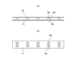
- FIG. 1 It is a front view which shows the schematic structure of one Embodiment of the bonding apparatus by this invention. It is a figure which shows the repair LED used for the bonding apparatus of this invention, (a) is a plan view, (b) is a front view. It is a figure which shows the carrier tape used for the bonding apparatus of this invention, (a) is a front view, (b) is a plan view which a protective film is removed. It is an enlarged front view of the main part of the bonding apparatus by this invention. It is explanatory drawing which shows the shape of the pressing member used in the bonding apparatus of this invention.
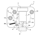
- FIG. 1 is a front view showing a schematic configuration of an embodiment of a bonding apparatus according to the present invention.
- This bonding device 1 is used in a repair device, and is intended to attach a non-defective electronic component to a repair region which is a region in which defective electronic components are removed in a circuit board.
- the stage 2 and a transfer mechanism are used.
- a flux coating device 4 an observation device 5, an elevating mechanism 6, and a heating device 7 are provided.
- the electronic component is a micro LED (Light Emitting Diode) (hereinafter, simply referred to as “LED”) will be described.
- LED Light Emitting Diode
- the stage 2 attracts and holds the back surface of the display panel (circuit board) 9 on which a plurality of LEDs 8 are arranged in a matrix and mounted on the opposite side to the mounting surface 2a. It moves in the XY plane orthogonal to the optical axis of the objective lens 10 of the observation device 5 described later, moves up and down in the Z direction perpendicular to the XY plane, and rotates around the central axis of the mounting surface 2a ( ⁇ ).
- the display panel 9 is provided with an LED 8 and a thin film transistor for driving the LED 8 in an intersecting region of a plurality of scanning lines and data lines provided at the intersection, and even a hard substrate made of glass or the like is made of polyimide. It may be a flexible substrate made of the above.
- a transfer mechanism 3 is provided above the stage 2. As shown in FIG. 2, the transfer mechanism 3 holds a plurality of repair LEDs 8A having an electrode portion 8a soldered by a solder material 34 on an end surface 8b opposite to the electrode portion 8a in the long axis direction.
- a carrier tape 11 such as a UV release tape, an adhesive tape, or a heat release tape, which is held side by side, is transferred in the long axis direction, and is a delivery reel 12, a take-up reel 13, and a separator reel 14. And a plurality of guide rollers 15.
- FIG. 3A shows a protective film 16 for protecting the electrode portion 8a of the repair LED 8A.
- FIG. 3B shows a carrier tape 11 having repair LEDs 8A arranged in a row in the long axis direction, but the carrier tape 11 has a plurality of repair LEDs 8A in a plurality of rows in the long axis direction. It may be provided side by side.
- the transmission reel 12 intermittently transmits the carrier tape 11 wound up with the electrode portion 8a of the repair LED 8A as the outside.
- the carrier tape 11 controls the drive of the transmission reel motor (not shown). It is possible to give a certain amount of back tension to the reel.
- the take-up reel 13 winds the carrier tape 11 lifted off by the repair LED 8A by a fixed amount, and is driven by a take-up reel motor (not shown) to rotate in the take-up direction. There is.
- the separator reel 14 is rotationally driven by a reel motor (not shown), and the protective film 16 peeled off from the repair LED 8A of the carrier tape 11 is wound up by a fixed amount according to the delivery amount of the carrier tape 11. It has become.
- the guide rollers 15 are intended to regulate both ends parallel to the long axis of the carrier tape 11 to keep the carrier tape 11 transferred stably, and a plurality of guide rollers 15 are provided at appropriate positions as needed. ing.
- a flux coating device 4 is provided on the transmission side of the carrier tape 11.
- the flux application device 4 applies the flux 17 to the electrode portion 8a of the repair LED 8A from which the protective film 16 has been peeled off, and is provided with a nozzle 18 facing the carrier tape 11 as shown in FIG.
- the flux 17 can be sprayed from the nozzle 18 onto the electrode portion 8a of the repair LED 8A.
- a recovery unit 19 for recovering the flux 17 is provided on the downstream side surface of the carrier tape 11 of the flux coating device 4 in the transfer direction in case the flux is excessively applied.
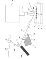
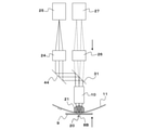
- An observation device 5 is provided above the stage 2 on the downstream side of the carrier tape 11 of the flux coating device 4 in the transfer direction. As shown in FIG. 4, the observation device 5 observes and aligns the processed repair LED 8B coated with the flux 17 with the repair area 20 of the display panel 9, and as shown in FIG. From the mounting surface 2a side of the stage 2, the pressing member 21, the objective lens 10, and the observation optical system 22 (see FIG. 7) are provided.
- the pressing member 21 is made of a transparent glass member such as quartz, and is fixedly provided.
- the LED 8B for repair which has been treated in combination with the rise of the stage 2, is connected to the display panel via the carrier tape 11. It is designed to be in pressure contact with the repair area 20 of 9.
- the pressing member 21 has an upper surface 21a on the objective lens 10 side and a lower surface 21b on which the carrier tape 11 slides, and the upper surface 21a has a focal position C of the objective lens 10. It is formed on a curved surface represented by a radius of curvature at the center, and the lower surface 21b is formed on a cylindrical surface having a central axis intersecting the transfer direction of the carrier tape 11.
- the light (illumination light) transmitted through the objective lens 10 passes through the pressing member 21 and is focused on the focal position C of the objective lens 10 that matches the observation surface 23. Then, the reflected light reflected from the observation surface 23 forms a spherical wave SW, passes through the pressing member 21 again, and returns to the objective lens 10.
- FIG. 6 is an explanatory diagram regarding the shape of the upper surface 21a of the pressing member 21.
- FIG. 6A illustrates a case where the upper surface 21a of the pressing member 21 has a curved surface shape having a curvature corresponding to the spherical wave SW of the reflected light.
- the wavefront of the spherical wave SW does not change on the upper surface 21a of the pressing member 21. That is, since light refraction does not occur on the upper surface 21a, aberration does not occur.
- FIG. 6B illustrates a pressing member 21'in which the upper surface 21a'has a planar shape, unlike the shape of the upper surface 21a of the pressing member 21.
- the upper surface 21a' is a planar shape
- light refraction occurs on the upper surface 21a'
- aberration occurs. Therefore, the resolution of the optical system is lowered, which hinders high-precision positioning.
- the shape of the lower surface 21b of the pressing member 21 is preferably a flat surface from an optical point of view. However, as long as the optical path difference in the field of view is within the range within the depth of focus of the objective lens 10, there is no problem even with a curved surface.
- the lower surface 21b is formed on a cylindrical surface having a central axis intersecting the transfer direction of the carrier tape 11.
- An objective lens 10 is provided above the pressing member 21.
- the objective lens 10 concentrates the illumination light on the observation surface 23, and the end surface 8b (observation surface 23) of the processed repair LED 8B cooperates with the first imaging lens 24 of the observation optical system 22 described later.
- the image is formed on the imaging surface of the first observation camera 25, and the repair region 20 (observation surface 23) of the display panel 9 is combined with the second imaging lens 26 of the observation optical system 22 to form a second observation camera.
- the image is formed on the imaging surface of 27.
- An observation optical system 22 is provided above the objective lens 10.
- the observation optical system 22 acquires an image of the end face 8b of the processed repair LED 8B and an image of the repair area 20 of the display panel 9, and controls the drive of the stage 2 in the XY direction so that both images match each other.
- the first optical path 28 from the objective lens 10 to the first observation camera 25 and the second optical path from the objective lens 10 to the second observation camera 27 are used for alignment. 29, and an optical path 30 for illuminating the observation surface 23 via the objective lens 10.
- the observation optical system 22 cooperates with the objective lens 10 on the first optical path 28 from the objective lens 10 to the first observation camera 25, and the processed repair LED 8B
- a first imaging lens 24 that forms an image on the image pickup surface of the first observation camera 25 is fixedly provided with the end surface 8b of the above.
- the second optical path 29 branched by the first half mirror 31 between the objective lens 10 and the first imaging lens 24 in the first optical path 28 from the objective lens 10 to the first observation camera 25.
- a second imaging lens 26 for forming a repair region 20 of the display panel 9 on the imaging surface of the second observation camera 27 in cooperation with the objective lens 10 is provided above.
- the second imaging lens 26 can move in the optical axis direction as the stage 2 rises while maintaining the imaging (best focus) of the repair region 20 of the display panel 9.
- an optical path (illumination system optical path 30) branched by a second half mirror 32 between the objective lens 10 and the first half mirror 31 in the first optical path 28 from the objective lens 10 to the first observation camera 25. )
- An illumination light source 33 is provided, and the repair LED 8B and the repair area 20 of the display panel 9 that have been processed are irradiated with visible light via the objective lens 10, the pressing member 21, and the carrier tape 11, and the processing has been completed.
- the end face 8b of the repair LED 8B and the repair area 20 of the display panel 9 can be observed by the first and second observation cameras 25 and 27.
- the stage 2 is provided with an elevating mechanism 6.
- the elevating mechanism 6 is for raising and lowering the stage 2 to press-contact and release the processed repair LED 8B to the repair area 20 of the display panel 9, and is an electric stage or an air cylinder that moves the stage 2 in the Z direction. And so on.
- a heating device 7 is provided integrally with the observation device 5.
- the heating device 7 heats and melts the solder material 34 (see FIG. 2) of the electrode portion 8a of the treated repair LED 8B to electrically melt the treated repair LED 8B on the electrode pad of the repair region 20 of the display panel 9. It is to be joined, and the processed repair LED 8B can be irradiated with infrared rays via the objective lens 10, the pressing member 21, and the carrier tape 11.
- the heating device 7 has an infrared ray on an optical path 36 branched by a prism 35 having a half mirror on the slope of the illumination system optical path 30 from the objective lens 10 to the illumination light source 33. It is equipped with a laser 37.
- reference numeral 38 indicates that ions are emitted toward the carrier tape 11 on the upstream side of the carrier tape 11 of the flux coating device 4 in the transfer direction to neutralize and remove the static electricity of the charged carrier tape 11.
- Ionizer Further, in FIG. 7, reference numeral 39 is a collimating lens that collimates the laser beam emitted from the infrared laser 37 and has an enlarged diameter, and reference numeral 40 is an end face 8b of the repair LED 8B that has been processed with the collimated laser beam. It is a slit for shaping according to the shape of the above, and reference numeral 41 is an imaging lens for forming an image on the end face 8b of the processed repair LED 8B in cooperation with the objective lens 10.
- reference numeral 42 is a guide illumination light source for adjusting the optical path 36 so that the laser beam emitted from the infrared laser 37 accurately irradiates the end face 8b of the processed repair LED 8B
- reference numeral 43 is a guide illumination light source. It is a half mirror prism for branching the optical path leading to the light source 42 from the optical path 36.
- Reference numeral 44 is a total reflection mirror for bending the optical path by 90 °.
- FIG. 8 is a front view showing a schematic configuration of a first embodiment of a repair device using the bonding device 1 of the present invention.
- the LED removing device 45 is provided side by side with the bonding device 1.
- the LED removing device 45 irradiates a defective LED 8 of a display panel 9 on which a plurality of LEDs 8 are mounted with a laser beam to remove the defective LED 8 to form a repair region 20 in the display panel 9, and is an observation optical system unit. It is configured to include a 46 and a laser optical system unit 47.
- the observation optical system unit 46 acquires an image of the defective LED 8 of the display panel 9 via the objective lens 48, controls the movement of the stage 2 based on the image data of the acquired image, and makes the defective LED 8 the objective lens. It is positioned at the center of the field of view of 48, and has the same optical configuration as the observation optical system 22 of the bonding device 1.
- the observation optical system unit 46 includes an imaging lens that forms an image of the defective LED 8 on the imaging surface of the observation camera in cooperation with the objective lens 48 on the optical path from the objective lens 48 to the observation camera.
- the illumination light source is provided on the optical path branched by the half mirror in the optical path from the objective lens 48 to the imaging lens.
- the imaging lens may be fixedly provided or may be provided so as to be movable along the optical axis. When the imaging lens is provided so as to be movable, the autofocus function can be realized.
- the laser optical system unit 47 irradiates the defective LED 8 with laser light via the objective lens 48 to sublimate and remove the defective LED 8, and removes the defective LED 8 by ultraviolet rays (near ultraviolet rays or far ultraviolet rays), infrared rays, or second harmonics. It is equipped with a laser that emits (SHG). In this case, lasers having a single wavelength may be individually provided and used by switching, or the fundamental wave may be wavelength-converted to generate high-order harmonics and laser light having a required wavelength may be output.
- the laser optical system unit 47 has the same optical configuration as the heating device 7 of the bonding device 1, and reflects another half mirror in the optical path toward the illumination light source or visible light to emit ultraviolet rays.
- a laser is provided on an optical path branched by a transmitted wavelength selectivity mirror.
- a slit for shaping the laser beam according to the shape of the end surface 8b of the LED 8 is provided on the optical path toward the laser, and the slit is formed into an image on the defective LED 8 in cooperation with the objective lens 48.
- An image lens is provided.
- the focal position of the objective lens 48 differs depending on the wavelength of the laser light used, it is desirable to provide a plurality of objective lenses 48 according to the wavelength used when switching and using laser light having a plurality of wavelengths.
- the first objective lens 48A for infrared rays and SHG, the second objective lens 48B for near ultraviolet rays, and the third objective lens 48C for far ultraviolet rays are attached to the revolver 49 and used by switching.
- the LED removing device 45 which can be used is illustrated.
- reference numeral 50 is a blow / suction unit that blows and sucks the sublimated LED 8 to remove it so as to suppress the generation of debris in the repair region 20, and faces the objective lens 48.
- the opening 51 is provided.
- step S1 a lighting inspection of a plurality of LEDs 8 mounted on the display panel 9 is performed, and the quality of the LEDs 8 is determined.
- the lighting inspection of the LED 8 is carried out by a lighting inspection device provided independently of the repair device. Specifically, using the alignment device provided in the lighting inspection device, alignment is performed so that the XY coordinate axes of the display panel 9 mounted on the stage and the XY coordinate axes of the lighting inspection device match, and then the display is displayed.
- the panel 9 Energize the panel 9 to turn on all of the plurality of LEDs 8, or if the panel 9 is equipped with three colors of red, green, and blue, turn on each color, and take a picture with an image sensor such as CCD or CMOS. A lighting inspection is carried out.
- the image sensor may be a fixed camera or a line sensor that shoots while moving from one end of the display panel 9 toward the other end.
- a pass / fail judgment is made based on the captured image of the image sensor. For example, when the lighting brightness of the LED 8 is equal to or higher than a predetermined reference value and the emission wavelength is within the predetermined wavelength band, it is determined to be a good product, and when the lighting brightness is below the above reference value, when it is not lit, or when it emits light. When the wavelength deviation exceeds the permissible range, it is determined to be a defective product. Then, when the defective LED 8 is detected, the position coordinates of the defective LED 8 are obtained from the number of rows and columns with respect to the reference position (for example, the center pixel of the panel) preset in the display panel 9, and the position coordinates are the removable media. Is remembered in.
- the data of the above position coordinates is stored in the storage unit of the control unit provided in each device or the data server connected to the network. It may be stored so that the data of the position coordinates can be shared between the devices.
- each device can share data via a data server connected to a network.
- step S2 When the defective LED 8 is not detected (“NO” determination) in step S2, the repair step of the display panel 9 is completed. On the other hand, when the defective LED 8 is detected (“YES” determination), the process proceeds to the repair step using the repair device of the first embodiment, step S3 is executed, and the defective LED 8 is removed from the display panel 9.
- step S3 first, the display panel 9 is attracted and held on the mounting surface 2a of the stage 2 of the repair device, and is positioned directly below the LED removing device 45.
- the LED removing device 45 alignment is performed using an alignment device (not shown) so that the XY coordinate axes of the display panel 9 and the XY coordinate axes of the LED removing device 45 match.
- the LED removing device 45 reads out the position coordinates of the defective LED 8 detected by the lighting inspection device from the data server, and is selected based on the position coordinates (when a plurality of defective LEDs 8 are present).
- One defective LED 8) is positioned at the irradiation position of the laser beam of the LED removing device 45.
- the elevating mechanism 6 controls the elevating and lowering of the stage 2 to focus on the end face 8b of the defective LED 8, and the stage 2 is slightly moved in the XY direction to irradiate the laser beam.
- the position of the defective LED 8 with respect to the position is finely adjusted.
- ultraviolet rays near ultraviolet rays or far ultraviolet rays
- the defective LED 8 is irradiated with the laser light of the ultraviolet rays shaped according to the shape of the end face 8b of the defective LED 8 by the slit. ..
- the defective LED 8 is ablated and removed, and the repair area 20 is formed on the display panel 9.
- the defective LED 8 may be irradiated with infrared rays, second harmonic generation (SHG), or the like, or ultraviolet rays may be irradiated with infrared rays or SHG in combination.
- the position coordinates of the repair area 20 which is the area where the defective LED 8 is removed in the display panel 9 are stored in the data server.
- the second defective LED 8 is present, the second defective LED 8 is positioned at the irradiation position of the laser beam based on the position coordinates of the second defective LED 8 read from the data server. Then, in the same manner as described above, the second defective LED 8 is removed, and the position coordinates of the repair area 20 are stored in the data server.
- step S4 the non-defective LED 8 is attached to the repair area 20 of the display panel 9 using the bonding device 1, and the bonding process is completed.
- the lighting inspection of the display panel 9 may be performed again by the lighting inspection device by returning to step S1 as necessary.
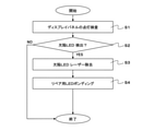
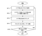
- FIG. 10 is a flowchart showing a bonding process performed by using the bonding device 1, and shows a specific process of step S4.
- the stage 2 is moved and the repair area 20 of the display panel 9 (in the case where a plurality of repair areas 20 exist, one selected repair area 20) is the repair area 20 read from the data server. It is positioned in the field of view of the objective lens 10 of the observation optical system 22 of the bonding device 1 based on the position coordinates, and bonding is started.
- the surface of the display panel 9 is observed using the second observation camera 27, and the second imaging lens 26 is shifted in the optical axis direction so that the image in the repair region 20 becomes clear and autofocused. Is carried out.
- step S11 of FIG. 10 the flux 17 is sprayed from the flux coating device 4 toward the repair LED 8A held by the carrier tape 11 (for example, the adhesive tape) and the protective film 16 is peeled off, and the repair LED 8A is soldered.
- the flux 17 is applied to the treated electrode portion 8a.
- step S12 as shown in FIG. 4, the carrier tape 11 is transferred by a predetermined amount, and the treated repair LED 8B coated with the flux 17 is placed in the field of view of the objective lens 10 directly under the pressing member 21. Positioned inside.
- the end surface 8b of the processed repair LED 8B is the imaging surface of the first observation camera 25 via the carrier tape 11, the pressing member 21, the objective lens 10, and the first imaging lens 24. Is imaged in.
- the repair region 20 of the display panel 9 is imaged on the imaging surface of the second observation camera 27 via the carrier tape 11, the pressing member 21, the objective lens 10, and the second imaging lens 26.
- the image data of the end face 8b of the processed repair LED 8B photographed and acquired by the first observation camera 25 and the image data photographed and acquired by the second observation camera 27 is compared with the image data, and the misalignment amount and the misalignment direction of both images are calculated. Then, the stage 2 is finely moved in the X and Y directions so that both images match, and alignment is performed.
- step S13 when the alignment is completed, the stage 2 is raised, and the electrode portion 8a of the processed repair LED 8B is pressed against the electrode pad of the repair region 20 of the display panel 9.
- the second imaging lens 26 is shifted in the direction of the arrow shown in FIG. 12, and the imaging state (best focus state) of the repair region 20 of the display panel 9 in the second observation camera 27 is achieved. ) Is maintained.
- step S14 the infrared laser 37 of the heating device 7 is driven, and the infrared laser beam shaped by the slit 40 according to the shape of the end face 8b of the LED 8 presses the objective lens 10, the pressing member 21, and the carrier tape 11.
- the end face 8b of the processed repair LED 8B is irradiated through.
- the solder material 34 of the electrode portion 8a of the treated repair LED 8B is heated and melted, and the electrode portion 8a of the LED 8 is electrically bonded to the electrode pad of the repair region 20 of the display panel 9.
- the flux 17 is applied to the solder material 34 on the electrode portion 8a of the LED 8, the surface of the solder material 34 and the surface of the repair region 20 are cleaned, and electrical connection failure is eliminated. Ru.
- the stage 2 is lowered.
- the treated repair LED 8B is used for the treated repair due to the difference in strength between the bonding strength of the solder material 34 and the adhesive strength of the adhesive tape.
- the LED 8B is lifted off from the carrier tape 11.
- step S15 it is determined whether or not further repair processing is necessary. That is, it is determined whether or not there is another repair region 20. Then, when there is no other repair region 20, the step S15 is determined to be "NO", and the bonding step using the bonding device 1 is completed. On the other hand, when a plurality of repair areas 20 are present, step S15 is a “YES” determination. At the same time, the stage 2 is moved in the XY direction based on the position coordinates of the second repair area 20, and the second repair area 20 is positioned at the joining position of the bonding device 1.
- step S11 the flux 17 is sprayed from the flux coating device 4 toward the second repair LED 8A from which the protective film 16 has been peeled off, and the soldered electrode portion 8a of the second repair LED 8A is obtained. Flux 17 is applied to the solder. After that, the repair process for the second repair area 20 is performed in the same manner as described above. Then, steps S11 to S15 are repeatedly executed until the repair processing for all the repair areas 20 is completed, the repair areas 20 do not exist, and the determination in step S15 is "NO".
- FIG. 13 is a front view showing a schematic configuration of a second embodiment of the repair device according to the present invention.
- the repair device includes a lighting inspection device 52.
- the lighting inspection device 52 has the same configuration as the lighting inspection device described in the first embodiment, and energizes the display panel 9 to determine the quality of the plurality of LEDs 8 and positions the defective LEDs 8. Can be obtained. And, it is provided integrally with the LED removing device 45 and the bonding device 1.
- the stage 2 is moved, and the display panel 9 attracted and held by the stage 2 is positioned in the photographing area of the image sensor 53 of the lighting inspection device 52.
- alignment is performed so that the XY coordinate axes of the display panel 9 and the XY coordinate axes of the lighting inspection device 52 match using an alignment device (not shown).
- a plurality of LEDs 8 of the display panel 9 are turned on, and an image sensor 53 is used to take a picture to inspect whether or not a defective LED 8 such as non-lighting is present.
- the position coordinates of the defective LED 8 are acquired, and the data of the position coordinates of the defective LED 8 is stored in a storage unit (not shown) of the repair device.
- the stage 2 moves and the display panel 9 is transported to just below the LED removing device 45.
- the data of the position coordinates of the defective LED 8 is read out from the storage unit of the repair device, and based on the position coordinates, the defective LED 8 on the display panel 9 (if a plurality of defective LEDs 8 are present, the defective LED 8 is selected. Only one defective LED 8) is positioned at the irradiation position of the laser beam of the LED removing device 45. Further, in the LED removing device 45, the stage 2 is moved up and down while observing the defective LED 8 by the observation camera of the observation optical system unit 46, and the end face 8b of the defective LED 8 is focused.
- the defective LED 8 is irradiated with the laser light of the ultraviolet rays shaped according to the shape of the end face 8b of the defective LED 8 by the slit.
- the defective LED 8 is ablated and removed, and the repair area 20 is formed on the display panel 9.
- the stage 2 moves and the display panel 9 is conveyed to just below the bonding device 1.
- the bonding device 1 the stage 2 is moved based on the position coordinates of the defective LED 8 read from the storage unit of the repair device, and the repair area 20 of the display panel 9 (when a plurality of repair areas 20 exist, the stage 2 is selected. Only one repair area 20) is positioned within the field of view of the objective lens 10 of the bonding device 1.
- the carrier tape 11 having a plurality of repair LEDs 8A having the soldered electrode portions 8a arranged in the major axis direction while holding the end faces 8b on the opposite side of the electrode portions 8a is the long axis.
- the flux is applied to the electrode portion 8a of the repair LED 8A from which the protective film 16 has been peeled off.
- the processed repair LED 8B coated with the flux 17 and the repair area 20 of the display panel 9 are observed by the first and second observation cameras 25 and 27, and both are observed based on the acquired image data of both images.
- Stage 2 is finely moved so that the images match, and alignment is performed. Subsequently, the stage 2 rises and the processed repair LED 8B is pressed against the repair area 20 of the display panel 9.
- the solder material 34 of the electrode portion 8a of the treated repair LED 8B is heated and melted by the infrared laser beam emitted from the heating device 7, and the treated repair LED 8B is electrically bonded to the repair region 20 of the display panel 9.
- the solder material 34 is heated and melted to join the repair LED 8A to the repair region 20 of the display panel 9. At that time, the surface of the solder material 34 and the debris in the repair region 20 of the display panel 9 are cleaned by the heated flux 17, and the occurrence of electrical connection failure can be eliminated. Further, as compared with the method of applying the flux 17 to the display panel 9, it is not necessary to wash and remove the excess flux 17 on the display panel 9 after connecting the repair LED 8A to the display panel 9, and the repair work can be performed. It will be easier.
- the present invention is not limited to this, and the electronic component may be any electronic component such as a mini LED or a semiconductor chip. Therefore, the circuit board is not limited to the display panel 9.
Landscapes
- Engineering & Computer Science (AREA)
- Manufacturing & Machinery (AREA)
- Microelectronics & Electronic Packaging (AREA)
- Electric Connection Of Electric Components To Printed Circuits (AREA)
- Supply And Installment Of Electrical Components (AREA)
- Wire Bonding (AREA)
Abstract
ボンディング装置1は、はんだ処理された電極部8aを有する複数のリペア用LED8Aの電極部8aとは反対側の端面8bを保持して長軸方向に移送されるキャリアテープ11のリペア用LED8Aを、複数のLED8を実装したディスプレイパネル9上の指定されたリペア領域20に電気的に接合する。ボンディング装置1は、リペア用LED8Aがリペア領域20に接合される接合位置のキャリアテープ11の移送方向上流側には、リペア用LED8Aの電極部8aにフラックス17を塗布するフラックス塗布装置4が設けられているものである。
Description
本発明は、回路基板に電子部品を実装するボンディング装置に関し、特に、はんだ処理された電子部品の電極部のはんだ材表面及び回路基板表面の洗浄化並びに電気的接続不良を排除し得るボンディング装置、リペア装置及びリペア方法に係るものである。
従来のリペア装置に使用されるボンディング装置は、基板上に配置された多数のLEDの中から検出された欠陥LEDが除去された基板の欠陥発生領域に新規導電性ボンディング材を提供し、新規導電性ボンディング材の上に新規LEDを安着させ、新規導電性ボンディング材を加熱して新規LEDと基板とを結合するものとなっている(例えば、特許文献1参照)。
しかし、このような従来のボンディング装置において、ボンディング材としてはんだ材が使用されるときには、はんだ材の表面に酸化膜が形成されて新規LEDの電極部と基板の電極部との接続不良が発生する問題があった。
このような問題に対しては、基板にフラックスを塗布してはんだ材表面の酸化膜を除去することが考えられる。しかしながら、この場合、新規LEDを基板に接続した後に基板上の余分なフラックスを洗浄して除去する必要があり、リペア工程が煩雑になるという問題があった。
そこで、本発明は、このような問題に対処し、はんだ処理された電子部品の電極部のはんだ材表面及び回路基板表面の洗浄化並びに電気的接続不良を排除し得るボンディング装置、リペア装置及びリペア方法を提供することを目的とする。
上記目的を達成するために、本発明によるボンディング装置は、はんだ処理された電極部を有する複数のリペア用電子部品の前記電極部とは反対側の端面を保持して長軸方向に移送されるキャリアテープの前記リペア用電子部品を、複数の電子部品を実装した回路基板上の指定された領域に電気的に接合するボンディング装置であって、前記リペア用電子部品が前記指定された領域に接合される接合位置の前記キャリアテープの移送方向上流側には、前記リペア用電子部品の前記電極部にフラックスを塗布するフラックス塗布装置が設けられているものである。
本発明によるボンディング装置は、具体的には、複数の電子部品を実装した回路基板における欠陥電子部品が除去された領域であるリペア領域に良品の電子部品を接合するボンディング装置であって、前記回路基板の実装面とは反対側の裏面を保持するステージと、はんだ処理された電極部を有する複数のリペア用電子部品を前記電極部とは反対側の端面を保持して長軸方向に並べて有するキャリアテープを、前記長軸方向に移送する移送機構と、前記キャリアテープの送出側にて前記複数のリペア用電子部品の前記電極部にフラックスを塗布するフラックス塗布装置と、前記フラックスが塗布された処理済リペア用電子部品と前記回路基板の前記リペア領域とを観察して位置合わせする観察装置と、前記ステージを上昇させて前記処理済リペア用電子部品を前記回路基板の前記リペア領域に圧接する昇降機構と、前記処理済リペア用電子部品の前記電極部のはんだ材を加熱溶融させて前記処理済リペア用電子部品を前記回路基板の前記リペア領域に電気的に接合する加熱装置と、を備えて構成したものである。
また、本発明によるリペア装置は、複数の電子部品を実装した回路基板の欠陥電子部品にレーザ光を照射し、前記欠陥電子部品を除去して前記回路基板にリペア領域を形成すると共に、該リペア領域の位置座標を記憶する電子部品除去装置と、前記回路基板の実装面とは反対側の裏面を保持するステージ、はんだ処理された電極部を有する複数のリペア用電子部品を前記電極部とは反対側の端面を保持して長軸方向に並べて有するキャリアテープを、前記長軸方向に移送する移送機構、前記キャリアテープの送出側にて前記複数のリペア用電子部品の前記電極部にフラックスを塗布するフラックス塗布装置、前記フラックスが塗布された処理済リペア用電子部品と前記回路基板のリペア領域とを観察して位置合わせする観察装置、前記ステージを上昇させて前記処理済リペア用電子部品を前記回路基板のリペア領域に圧接する昇降機構、及び前記処理済リペア用電子部品の前記電極部のはんだ材を加熱溶融させて前記処理済リペア用電子部品を前記回路基板のリペア領域に電気的に接合する加熱装置を備えて構成したボンディング装置と、を備え、前記ステージは、前記電子部品除去装置と前記ボンディング装置との間を移動して前記リペア領域の前記位置座標に基づいて、前記リペア領域を前記ボンディング装置の前記処理済リペア用電子部品との接合位置に位置付けるように構成されている。
好ましくは、前記リペア装置は、前記回路基板に通電して複数の電子部品の良否を判定すると共に、欠陥電子部品の位置座標を記憶する点灯検査装置をさらに備え、前記ステージは、前記点灯検査装置と前記電子部品除去装置と前記ボンディング装置との間を移動して、前記欠陥電子部品の位置座標に基づいて前記欠陥電子部品を前記電子部品除去装置のレーザ光照射位置に位置付けると共に、前記リペア領域の位置座標に基づいて前記リペア領域を前記ボンディング装置の前記処理済リペア用電子部品との接合位置に位置付けるように構成するとよい。
さらに、本発明によるリペア方法は、複数の電子部品を実装した回路基板の実装面とは反対側の裏面をステージに保持する第1ステップと、はんだ処理された電極部を有する複数のリペア用電子部品を前記電極部とは反対側の端面を保持して長軸方向に並べて有するキャリアテープを、前記長軸方向に移送する第2ステップと、前記複数のリペア用電子部品の前記電極部にフラックスを塗布する第3ステップと、前記フラックスが塗布された処理済リペア用電子部品と前記回路基板における欠陥電子部品が除去された領域であるリペア領域とを観察して位置合わせする第4ステップと、前記処理済リペア用電子部品を前記回路基板の前記リペア領域に圧接する第5ステップと、前記処理済リペア用電子部品の前記電極部のはんだ材を加熱溶融させて前記処理済リペア用電子部品を前記回路基板の前記リペア領域に電気的に接合する第6ステップと、を行うものである。
好ましくは、前記リペア方法は、第1ステップの実施前に、前記回路基板に通電して複数の電子部品の良否を判定すると共に、不良と判定された欠陥電子部品にレーザ光を照射し、前記欠陥電子部品を除去して前記回路基板に前記リペア領域を形成するステップを実施するとよい。
本発明によれば、はんだ処理された電子部品の電極部にフラックスを塗布するようにしているので、はんだ材を加熱溶融して電子部品を回路基板の所定の領域に接合する際に、加熱されたフラックスによりはんだ材の表面及び回路基板の上記所定の領域のデブリが洗浄化され、電気的接続不良の発生を排除することができる。また、回路基板にフラックスを塗布する方法と比較して、電子部品を回路基板に接続した後に回路基板の余分なフラックスを洗浄して除去する必要がなく、ボンディング作業が容易になる。
以下、本発明の実施形態を添付図面に基づいて詳細に説明する。図1は本発明によるボンディング装置の一実施形態の概略構成を示す正面図である。このボンディング装置1は、リペア装置において使用されるもので、回路基板における欠陥電子部品が除去された領域であるリペア領域に良品の電子部品を取り付けようとするものであり、ステージ2と、移送機構3と、フラックス塗布装置4と、観察装置5と、昇降機構6と、加熱装置7と、を備えて構成されている。以下、電子部品がマイクロLED(Light Emitting Diode)(以下、単に「LED」という)である場合について説明する。
上記ステージ2は、図4に示すように、複数のLED8をマトリクス状に配置して実装したディスプレイパネル(回路基板)9の実装面とは反対側の裏面を載置面2aに吸着して保持するものであり、後述する観察装置5の対物レンズ10の光軸に直交するXY平面内を移動し、XY平面に垂直なZ方向に昇降し、載置面2aの中心軸回りに回動(θ)するようになっている。
上記ディスプレイパネル9は、交差して設けられた複数の走査線及びデータ線の交差領域に、LED8及びそれを駆動する薄膜トランジスタを備えたものであり、ガラス等からなるハード基板であっても、ポリイミド等からなるフレキシブル基板であってもよい。
上記ステージ2の上方には、移送機構3が設けられている。この移送機構3は、図2に示すように、はんだ材34によりはんだ処理された電極部8aを有する複数のリペア用LED8Aを電極部8aとは反対側の端面8bを保持して長軸方向に並べて有する、例えばUV剥離テープ、粘着テープ又は熱剥離テープ等のキャリアテープ11(図3を参照)を長軸方向に移送するものであり、送出リール12と、巻取リール13と、セパレータリール14と、複数のガイドローラ15と、を備えて構成されている。
なお、キャリアテープ11には、図3(a)に示すように、リペア用LED8Aの電極部8aを保護する保護フィルム16が貼付されている。また、図3(b)には、キャリアテープ11の長軸方向に一列に並べてリペア用LED8Aを備えたものが示されているが、キャリアテープ11にはリペア用LED8Aが長軸方向に複数列に並べて備えられていてもよい。
ここで、上記送出リール12は、リペア用LED8Aの電極部8aを外側として巻き上げられたキャリアテープ11を間欠的に送出するもので、例えば図示省略の送出リールモータの駆動を制御してキャリアテープ11に一定のバックテンションを付与できるようになっている。また、上記巻取リール13は、リペア用LED8Aがリフトオフされたキャリアテープ11を一定量ずつ巻き取るものであり、図示省略の巻取リールモータにより駆動されて巻取方向に回転するようになっている。さらに、上記セパレータリール14は、図示省略のリールモータにより回転駆動され、キャリアテープ11のリペア用LED8Aから剥がされた保護フィルム16を、キャリアテープ11の送出量に応じて一定量ずつ巻き取るようになっている。そして、ガイドローラ15は、キャリアテープ11の長軸に平行な両端部を規制してキャリアテープ11の移送を安定に保つためのものであり、必要に応じて適宜の位置に複数個が設けられている。
キャリアテープ11の送出側には、フラックス塗布装置4が設けられている。このフラックス塗布装置4は、保護フィルム16が剥がされたリペア用LED8Aの電極部8aにフラックス17を塗布するものであり、図4に示すようにキャリアテープ11に対面してノズル18を備え、該ノズル18からフラックス17をリペア用LED8Aの電極部8aに噴霧できるようになっている。また、フラックス塗布装置4のキャリアテープ11の移送方向下流側側面には、フラックスが過剰に塗布された場合に備えて、フラックス17を回収する回収部19が設けられている。
上記フラックス塗布装置4のキャリアテープ11の移送方向下流側にてステージ2の上方には、観察装置5が設けられている。この観察装置5は、図4に示すように、フラックス17が塗布された処理済リペア用LED8Bとディスプレイパネル9のリペア領域20とを観察して位置合わせするものであり、図1に示すようにステージ2の載置面2a側から押圧部材21と、対物レンズ10と、観察光学系22(図7を参照)と、を備えて構成されている。
上記押圧部材21は、石英等の透明なガラス部材で形成されたものであり、固定して設けられており、ステージ2の上昇と相まって処理済リペア用LED8Bを、キャリアテープ11を介してディスプレイパネル9のリペア領域20に圧接するようになっている。詳細には、押圧部材21は、図5に示すように、対物レンズ10側の上面21aと、キャリアテープ11が摺動する下面21bとを有し、上面21aは対物レンズ10の焦点位置Cを中心とする曲率半径で表される曲面に形成され、下面21bはキャリアテープ11の移送方向に交差する中心軸を有するシリンドリカル面に形成されている。
この場合、図5に示すように、対物レンズ10を透過した光(照明光)は、押圧部材21を透過して、観察面23に合致した対物レンズ10の焦点位置Cに集光される。そして、観察面23から反射された反射光は、球面波SWを形成し、再び、押圧部材21を透過して対物レンズ10に戻って行く。
図6は押圧部材21の上面21aの形状に関する説明図である。図6(a)は、押圧部材21の上面21aが反射光の球面波SWに一致した曲率を有する曲面形状を有している場合を例示している。この場合、図5を用いて上述した通り、押圧部材21の上面21aにおいて球面波SWの波面が変化しない。即ち、上面21aでは光の屈折が起こらないため、収差が発生しない。図6(b)は、上記押圧部材21の上面21aの形状と異なり、上面21a′が平面形状を有している押圧部材21′を例示している。上面21a′が平面形状の場合、上面21a′で光の屈折が起こり、収差が発生する。そのため、光学系の分解能が低下し、高精度な位置決めの妨げとなる。
押圧部材21の下面21bの形状は、光学的な観点に立つと平面が望ましい。しかし、視野内での光路差が対物レンズ10の焦点深度内に収まる範囲内であれば、曲面でも問題がない。本発明においては、上述したように下面21bは、キャリアテープ11の移送方向に交差する中心軸を有するシリンドリカル面に形成されている。
上記押圧部材21の上方には、対物レンズ10が設けられている。この対物レンズ10は、照明光を観察面23に集光すると共に、処理済リペア用LED8Bの端面8b(観察面23)を後述の観察光学系22の第1の結像レンズ24と協働して第1の観察カメラ25の撮像面に結像し、ディスプレイパネル9のリペア領域20(観察面23)を観察光学系22の第2の結像レンズ26と協働して第2の観察カメラ27の撮像面に結像するものである。
上記対物レンズ10の上方には、観察光学系22が設けられている。この観察光学系22は、処理済リペア用LED8Bの端面8bの画像及びディスプレイパネル9のリペア領域20の画像を取得して、両画像が互いに合致するようにステージ2のXY方向への駆動を制御してアライメントするためのものであり、図7に示すように、対物レンズ10から第1の観察カメラ25に至る第1の光路28と、対物レンズ10から第2の観察カメラ27に至る第2の光路29と、対物レンズ10を介して観察面23を照明する照明系光路30とを備えて構成されている。
詳細には、観察光学系22は、図7に示すように、対物レンズ10から第1の観察カメラ25に至る第1の光路28上に対物レンズ10と協働して、処理済リペア用LED8Bの端面8bを第1の観察カメラ25の撮像面に結像する第1の結像レンズ24を固定して備えている。また、対物レンズ10から第1の観察カメラ25に至る第1の光路28における対物レンズ10と第1の結像レンズ24との間で第1のハーフミラー31により分岐された第2の光路29上には、対物レンズ10と協働してディスプレイパネル9のリペア領域20を第2の観察カメラ27の撮像面に結像する第2の結像レンズ26が備えられている。この場合、第2の結像レンズ26は、ディスプレイパネル9のリペア領域20の結像(ベストフォーカス)を維持しながらステージ2の上昇に伴って光軸方向に移動可能となっている。さらに、対物レンズ10から第1の観察カメラ25に至る第1の光路28における対物レンズ10と第1のハーフミラー31との間で第2のハーフミラー32により分岐された光路(照明系光路30)上には、照明光源33が設けられており、対物レンズ10、押圧部材21及びキャリアテープ11を介して処理済リペア用LED8B及びディスプレイパネル9のリペア領域20に可視光を照射し、処理済リペア用LED8Bの端面8b及びディスプレイパネル9のリペア領域20が第1及び第2の観察カメラ25,27で観察できるようになっている。
上記ステージ2には、昇降機構6が設けられている。この昇降機構6は、ステージ2を昇降させて処理済リペア用LED8Bをディスプレイパネル9のリペア領域20に圧接及び圧接解除するためのものであり、ステージ2をZ方向に移動させる電動ステージ又はエアシリンダ等である。
上記観察装置5と一体的に加熱装置7が設けられている。この加熱装置7は、処理済リペア用LED8Bの電極部8aのはんだ材34(図2を参照)を加熱溶融させて処理済リペア用LED8Bをディスプレイパネル9のリペア領域20の電極パッドに電気的に接合するものであり、対物レンズ10、押圧部材21及びキャリアテープ11を介して処理済リペア用LED8Bに赤外線を照射できるようになっている。具体的には、加熱装置7は、図7に示すように、対物レンズ10から照明光源33に向かう照明系光路30における斜面にハーフミラーを備えたプリズム35により分岐された光路36上に、赤外線レーザ37を備えたものである。
なお、図1において符号38は、フラックス塗布装置4のキャリアテープ11の移送方向上流側でキャリアテープ11に向けてイオンを放出し、帯電したキャリアテープ11の静電気を中和して除去するためのイオナイザである。また、図7において、符号39は、赤外線レーザ37から放出され、径が拡大されたレーザ光をコリメートするコリメートレンズであり、符号40は、コリメートされたレーザ光を処理済リペア用LED8Bの端面8bの形状に合わせて整形するためのスリットであり、符号41は、対物レンズ10と協働してスリットを処理済リペア用LED8Bの端面8bに結像するための結像レンズである。また、符号42は、赤外線レーザ37から放出されたレーザ光が処理済リペア用LED8Bの端面8bに正確に照射するように光路36を調整するためのガイド照明光源であり、符号43は、ガイド照明光源42に至る光路を光路36から分岐するためのハーフミラープリズムである。そして、符号44は、光路を90°折り曲げるための全反射ミラーである。
図8は本発明のボンディング装置1を使用するリペア装置の第1の実施形態の概略構成を示す正面図である。
上記第1の実施形態においては、ボンディング装置1に並べてLED除去装置45が設けられている。このLED除去装置45は、複数のLED8を実装したディスプレイパネル9の欠陥LED8にレーザ光を照射し、欠陥LED8を除去してディスプレイパネル9にリペア領域20を形成するものであり、観察光学系ユニット46と、レーザ光学系ユニット47と、を備えて構成されている。
上記第1の実施形態においては、ボンディング装置1に並べてLED除去装置45が設けられている。このLED除去装置45は、複数のLED8を実装したディスプレイパネル9の欠陥LED8にレーザ光を照射し、欠陥LED8を除去してディスプレイパネル9にリペア領域20を形成するものであり、観察光学系ユニット46と、レーザ光学系ユニット47と、を備えて構成されている。
上記観察光学系ユニット46は、対物レンズ48を介してディスプレイパネル9の欠陥LED8の画像を取得し、取得された画像の画像データに基づいてステージ2の移動を制御し、上記欠陥LED8を対物レンズ48の視野中心に位置付けるものであり、ボンディング装置1の観察光学系22と同様の光学構成となっている。具体的には、観察光学系ユニット46は、対物レンズ48から観察カメラに向かう光路上に対物レンズ48と協働して上記欠陥LED8を観察カメラの撮像面に結像する結像レンズを備え、対物レンズ48から結像レンズに向かう光路におけるハーフミラーにより分岐された光路上に照明光源を備えた構成となっている。この場合、上記結像レンズは、固定して備えてもよく、光軸に沿って移動可能に備えてもよい。結像レンズを移動可能に備えた場合には、オートフォーカス機能を実現することができる。
上記レーザ光学系ユニット47は、対物レンズ48を介して上記欠陥LED8にレーザ光を照射し、欠陥LED8を昇華させて除去するもので、紫外線(近紫外線又は遠紫外線)や赤外線又は第2高調波(SHG)を放出するレーザを備えている。この場合、単一波長のレーザを個別に備えて、切り替えて使用してもよく、基本波を波長変換して高次高調波を生成し、必要な波長のレーザ光を出力させてもよい。
上記レーザ光学系ユニット47は、具体的には、ボンディング装置1の加熱装置7と同様の光学構成となっており、上記照明光源に向かう光路における別のハーフミラー、又は可視光を反射し紫外線を透過する波長選択性ミラーにより分岐された光路上にレーザが備えられている。また、上記レーザに向かう光路上には、LED8の端面8bの形状に合わせてレーザ光を整形するためのスリットが設けられ、該スリットを対物レンズ48と協働して欠陥LED8に結像する結像レンズが設けられている。
使用するレーザ光の波長により対物レンズ48の焦点位置が異なるため、複数の波長のレーザ光を切り替えて使用する場合には、対物レンズ48は、使用する波長に応じて複数備えるのが望ましい。図8は、赤外線及びSHG用の第1の対物レンズ48Aと、近紫外線用の第2の対物レンズ48Bと、遠紫外線用の第3の対物レンズ48Cと、をレボルバー49に取り付けて切り替えて使用することができるようにしたLED除去装置45を例示している。なお、図8において符号50は、昇華したLED8をブロー及び吸引して除去し、リペア領域20にデブリが発生するのを抑制し得るようにしたブロー・吸引部であり、対物レンズ48に対向して開口51が設けられている。
次に、このように構成された上記第1の実施形態によるリペア装置を使用して行うリペア方法について、図9,10のフローチャートを参照して説明する。
先ず、図9に示すように、ステップS1においては、ディスプレイパネル9に実装された複数のLED8の点灯検査を実施し、LED8の良否が判定される。上記第1の実施形態においては、LED8の点灯検査は、上記リペア装置とは別に独立して備えた点灯検査装置により実施される。具体的には、点灯検査装置に備えるアライメント装置を使用して、ステージ上に載置されたディスプレイパネル9のXY座標軸と点灯検査装置のXY座標軸とが合致するようにアライメントを実施した後、ディスプレイパネル9に通電して複数のLED8を全点灯させ、又は赤、緑及び青の3色のLED8を備えている場合には色毎に点灯させ、それをCCDやCMOS等のイメージセンサにより撮影して点灯検査が実施される。なお、イメージセンサは、固定カメラであっても、ディスプレイパネル9の一方端から他方端に向かって移動しながら撮影するラインセンサであってもよい。
先ず、図9に示すように、ステップS1においては、ディスプレイパネル9に実装された複数のLED8の点灯検査を実施し、LED8の良否が判定される。上記第1の実施形態においては、LED8の点灯検査は、上記リペア装置とは別に独立して備えた点灯検査装置により実施される。具体的には、点灯検査装置に備えるアライメント装置を使用して、ステージ上に載置されたディスプレイパネル9のXY座標軸と点灯検査装置のXY座標軸とが合致するようにアライメントを実施した後、ディスプレイパネル9に通電して複数のLED8を全点灯させ、又は赤、緑及び青の3色のLED8を備えている場合には色毎に点灯させ、それをCCDやCMOS等のイメージセンサにより撮影して点灯検査が実施される。なお、イメージセンサは、固定カメラであっても、ディスプレイパネル9の一方端から他方端に向かって移動しながら撮影するラインセンサであってもよい。
次に、ステップS2において、イメージセンサの撮影画像に基づいて良否判定が行われる。例えば、LED8の点灯輝度が所定の基準値以上であり、発光波長が所定の波長帯域内にあるときには良品と判定され、点灯輝度が上記基準値を下回っているとき、不点灯のとき、又は発光波長のずれが許容範囲を超えているときには欠陥品と判定される。そして、欠陥LED8が検出されると、該欠陥LED8の位置座標をディスプレイパネル9に予め設定された基準位置(例えば、パネルの中心画素)に対する行数及び列数から求め、その位置座標がリムーバブルメディアに記憶される。又は、点灯検査装置がリペア装置と工場内のLAN(Enthernet)に接続されている場合には、上記位置座標のデータが各装置に備えられた制御ユニットの記憶部やネットワーク接続されたデータサーバに記憶され、上記位置座標のデータが装置間で共有できるようにしてもよい。なお、以下の説明においては、各装置がネットワーク接続されたデータサーバを介してデータを共有できるようになっている場合について説明する。
ステップS2において、欠陥LED8が検出されなかった(“NO”判定)ときには、ディスプレイパネル9のリペア工程が終了する。一方、欠陥LED8が検出された(“YES”判定)ときには、第1の実施形態のリペア装置を使用したリペア工程に進み、ステップS3が実行されてディスプレイパネル9から欠陥LED8が除去される。
具体的には、ステップS3においては、先ず、ディスプレイパネル9がリペア装置のステージ2の載置面2aに吸着保持され、LED除去装置45の真下の位置に位置付けられる。LED除去装置45においては、図示省略のアライメント装置を使用してディスプレイパネル9のXY座標軸とLED除去装置45のXY座標軸とが合致するようにアライメントが実施される。また、LED除去装置45は上記点灯検査装置において検出された欠陥LED8の位置座標を上記データサーバから読み出し、該位置座標に基づいて欠陥LED8(欠陥LED8が複数個存在する場合には、選択された1つの欠陥LED8)がLED除去装置45のレーザ光の照射位置に位置付けられる。さらに、観察光学系ユニット46により欠陥LED8を観察しながら、昇降機構6によるステージ2の昇降を制御して欠陥LED8の端面8bにフォーカスすると共に、ステージ2をXY方向に微動してレーザ光の照射位置に対する欠陥LED8の位置が微調整される。そして、レーザ光学系ユニット47のレーザから、例えば紫外線(近紫外線又は遠紫外線)が放出され、スリットによって欠陥LED8の端面8bの形状に合わせて整形された紫外線のレーザ光が欠陥LED8に照射される。これにより、欠陥LED8がアブレートされて除去され、リペア領域20がディスプレイパネル9に形成される。又は、欠陥LED8に赤外線や第2高調波(SHG)等を照射してもよく、又は紫外線と、赤外線又はSHGとを組み合わせて照射してもよい。このようにして欠陥LED8が除去されると、ディスプレイパネル9における欠陥LED8が除去された領域であるリペア領域20の位置座標がデータサーバに保存される。また、他に第2の欠陥LED8が存在するときには、上記データサーバから読み出した上記第2の欠陥LED8の位置座標に基づいて該第2の欠陥LED8がレーザ光の照射位置に位置付けられる。そして、上記と同様にして上記第2の欠陥LED8が除去され、そのリペア領域20の位置座標がデータサーバに保存される。
続いて、ステップS4において、ボンディング装置1を使用してディスプレイパネル9のリペア領域20に良品のLED8が取り付けられ、ボンディング工程が終了する。なお、ボンディング装置1を使用した上記ボンディング工程が終了すると、必要に応じてステップS1に戻って点灯検査装置によりディスプレイパネル9の点灯検査を改めて実施してもよい。
図10はボンディング装置1を使用して行うボンディング工程を示すフローチャートであり、上記ステップS4の具体的な工程を示すものである。
先ず、ステージ2が移動されてディスプレイパネル9のリペア領域20(リペア領域20が複数存在する場合には、選択された1つのリペア領域20)が、データサーバから読み出された上記リペア領域20の位置座標に基づいてボンディング装置1の観察光学系22の対物レンズ10の視野内に位置付けられ、ボンディングが開始される。この場合、第2の観察カメラ27を使用してディスプレイパネル9の表面が観察され、リペア領域20の画像が鮮明となるように第2の結像レンズ26を光軸方向にシフトしてオートフォーカスが実施される。
先ず、ステージ2が移動されてディスプレイパネル9のリペア領域20(リペア領域20が複数存在する場合には、選択された1つのリペア領域20)が、データサーバから読み出された上記リペア領域20の位置座標に基づいてボンディング装置1の観察光学系22の対物レンズ10の視野内に位置付けられ、ボンディングが開始される。この場合、第2の観察カメラ27を使用してディスプレイパネル9の表面が観察され、リペア領域20の画像が鮮明となるように第2の結像レンズ26を光軸方向にシフトしてオートフォーカスが実施される。
図10のステップS11においては、キャリアテープ11(例えば、粘着テープ)に保持され、保護フィルム16が剥がされたリペア用LED8Aに向けてフラックス塗布装置4からフラックス17が噴霧され、リペア用LED8Aのはんだ処理された電極部8aにフラックス17が塗布される。
次に、ステップS12においては、図4に示すように、キャリアテープ11が所定量だけ移送され、フラックス17が塗布された処理済リペア用LED8Bが押圧部材21の真下にて、対物レンズ10の視野内に位置付けられる。この場合、図11に示すように、処理済リペア用LED8Bの端面8bがキャリアテープ11、押圧部材21、対物レンズ10及び第1の結像レンズ24を介して第1の観察カメラ25の撮像面に結像される。一方、ディスプレイパネル9のリペア領域20は、キャリアテープ11、押圧部材21、対物レンズ10及び第2の結像レンズ26を介して第2の観察カメラ27の撮像面に結像されている。
ボンディング装置1の図示省略の制御部では、第1の観察カメラ25により撮影して取得された処理済リペア用LED8Bの端面8bの画像データと、第2の観察カメラ27により撮影して取得されたディスプレイパネル9のリペア領域20の画像データとが比較処理され、両画像の位置ずれ量及び位置ずれ方向が算出される。そして、両画像が合致するようにステージ2がX及びY方向に微動されてアライメントが実施される。
次いで、ステップS13においては、アライメントが終了するとステージ2が上昇され、処理済リペア用LED8Bの電極部8aがディスプレイパネル9のリペア領域20の電極パッドに圧接される。このとき、ステージ2の上昇に伴って第2の結像レンズ26が図12に示す矢印方向にシフトされ、第2の観察カメラ27におけるディスプレイパネル9のリペア領域20の結像状態(ベストフォーカス状態)が維持される。
次に、ステップS14において、加熱装置7の赤外線レーザ37が駆動され、スリット40によりLED8の端面8bの形状に合わせて整形された赤外線のレーザ光が対物レンズ10、押圧部材21及びキャリアテープ11を介して処理済リペア用LED8Bの端面8bに照射される。これにより、処理済リペア用LED8Bの電極部8aのはんだ材34が加熱溶融され、LED8の電極部8aがディスプレイパネル9のリペア領域20の電極パッドに電気的に接合される。このとき、LED8の電極部8a上のはんだ材34には、フラックス17が塗布されているため、はんだ材34の表面及び上記リペア領域20の表面の洗浄化がなされ、電気的接続不良が排除される。
リペア領域20に対するLED8のリペアが終了するとステージ2が下降する。このとき、ディスプレイパネル9のリペア領域20に接合された処理済リペア用LED8Bは、ステージ2と共に下降するため、はんだ材34による接合強度と粘着テープの粘着強度との強度差により、処理済リペア用LED8Bはキャリアテープ11からリフトオフされる。
続いて、ステップS15において、更なるリペア処理が必要か否かが判断される。即ち、他にリペア領域20が存在するか否かが判断される。そして、他にリペア領域20が存在しないときには、ステップS15は、“NO”判定となってボンディング装置1を使用したボンディング工程が終了する。一方、複数のリペア領域20が存在するときには、ステップS15は“YES”判定となる。同時に、第2のリペア領域20の位置座標に基づいてステージ2がXY方向に移動され、上記第2のリペア領域20がボンディング装置1の接合位置に位置付けられる。その後、ステップS11に戻って、保護フィルム16が剥がされた第2のリペア用LED8Aに向けてフラックス塗布装置4からフラックス17が噴霧され、上記第2のリペア用LED8Aのはんだ処理された電極部8aにフラックス17が塗布される。以後、上記と同様にして第2のリペア領域20に対するリペア処理が実施される。そして、全てのリペア領域20に対するリペア処理が終了し、他にリペア領域20が存在しなくなってステップS15が“NO”判定となるまでは、ステップS11~S15が繰り返し実施される。
図13は本発明によるリペア装置の第2の実施形態の概略構成を示す正面図である。
上記第1の実施形態と異なる点は、リペア装置が点灯検査装置52を備えていることである。この点灯検査装置52は、第1の実施形態で説明した点灯検査装置と同様の構成を有するものであり、ディスプレイパネル9に通電して複数のLED8の良否を判定すると共に、欠陥LED8の位置座標を取得できるようになっている。そして、LED除去装置45及びボンディング装置1と一体的に設けられている。
上記第1の実施形態と異なる点は、リペア装置が点灯検査装置52を備えていることである。この点灯検査装置52は、第1の実施形態で説明した点灯検査装置と同様の構成を有するものであり、ディスプレイパネル9に通電して複数のLED8の良否を判定すると共に、欠陥LED8の位置座標を取得できるようになっている。そして、LED除去装置45及びボンディング装置1と一体的に設けられている。
この第2の実施形態によれば、先ず、ステージ2が移動して、ステージ2に吸着保持されたディスプレイパネル9が点灯検査装置52のイメージセンサ53の撮影領域内に位置付けられる。このとき、図示省略のアライメント装置を使用してディスプレイパネル9のXY座標軸と点灯検査装置52のXY座標軸とが合致するようにアライメントが実施される。その後、ディスプレイパネル9の複数のLED8が点灯され、イメージセンサ53により撮影して不点灯等の欠陥LED8が存在するか否かが検査される。その結果、ディスプレイパネル9に欠陥LED8が存在する場合には、その欠陥LED8の位置座標が取得され、該欠陥LED8の位置座標のデータがリペア装置の図示省略の記憶部に保存される。
次に、ステージ2が移動してディスプレイパネル9がLED除去装置45の真下まで搬送される。LED除去装置45においては、欠陥LED8の位置座標のデータをリペア装置の記憶部から読み出し、該位置座標に基づいてディスプレイパネル9上の欠陥LED8(複数の欠陥LED8が存在する場合には、選択された1つの欠陥LED8)がLED除去装置45のレーザ光の照射位置に位置付けられる。さらに、LED除去装置45においては、観察光学系ユニット46の観察カメラにより欠陥LED8を観察しながらステージ2が昇降され、欠陥LED8の端面8bにフォーカスされる。そして、レーザ光学系ユニット47のレーザから、例えば紫外線が放出され、スリットによって欠陥LED8の端面8bの形状に合わせて整形された紫外線のレーザ光が欠陥LED8に照射される。これにより、欠陥LED8がアブレートされて除去され、リペア領域20がディスプレイパネル9に形成される。
LED除去装置45による欠陥LED8の除去が終了すると、ステージ2が移動してディスプレイパネル9がボンディング装置1の真下まで搬送される。ボンディング装置1においては、リペア装置の記憶部から読み出した欠陥LED8の位置座標に基づいてステージ2が移動され、ディスプレイパネル9のリペア領域20(複数のリペア領域20が存在する場合には、選択された1つのリペア領域20)がボンディング装置1の対物レンズ10の視野内に位置付けられる。さらに、ボンディング装置1においては、はんだ処理された電極部8aを有する複数のリペア用LED8Aを電極部8aとは反対側の端面8bを保持して長軸方向に並べて有するキャリアテープ11が上記長軸方向に移送される。次に、保護フィルム16が剥がされたリペア用LED8Aの電極部8aにフラックスが塗布される。次いで、フラックス17が塗布された処理済リペア用LED8Bとディスプレイパネル9のリペア領域20とを第1及び第2の観察カメラ25,27で観察し、取得された両画像の画像データに基づいて両画像が合致するようにステージ2が微動され、アライメントが実施される。続いて、ステージ2が上昇して処理済リペア用LED8Bがディスプレイパネル9のリペア領域20に圧接される。そして、加熱装置7から照射される赤外線レーザ光により処理済リペア用LED8Bの電極部8aのはんだ材34が加熱溶融され、処理済リペア用LED8Bがディスプレイパネル9のリペア領域20に電気的に接合される。
本発明によれば、はんだ処理されたリペア用LED8Aの電極部8aにフラックス17を塗布するようにしているので、はんだ材34を加熱溶融してリペア用LED8Aをディスプレイパネル9のリペア領域20に接合する際に、加熱されたフラックス17によりはんだ材34の表面及びディスプレイパネル9のリペア領域20のデブリが洗浄化され、電気的接続不良の発生を排除することができる。また、ディスプレイパネル9にフラックス17を塗布する方法と比較して、リペア用LED8Aをディスプレイパネル9に接続した後にディスプレイパネル9上の余分なフラックス17を洗浄して除去する必要がなく、リペア作業が容易になる。
なお、上記実施形態においては、電子部品がマイクロLED8の場合について説明したが、本発明はこれに限られず、電子部品は、ミニLEDや半導体チップ等、如何なる電子部品であってもよい。したがって、回路基板は、ディスプレイパネル9に限られない。
上記実施形態は、本発明が理解及び実施できる程度に概略的に示したものであり、本発明はこれに限定されるものではない。本発明は、特許請求の範囲に示された技術的思想の範囲を逸脱しない限り種々に変更及び修正をすることができる。
1…ボンディング装置
2…ステージ
3…移送機構
4…フラックス塗布装置
5…観察装置
6…昇降機構
7…加熱装置
8…LED(電子部品)
8a…電極部
8b…端面
8A…リペア用LED
8B…処理済リペア用LED
9…ディスプレイパネル(回路基板)
10…対物レンズ
11…キャリアテープ
17…フラックス
19…回収部
20…リペア領域
21…押圧部材
21a…上面
21b…下面
34…はんだ材
37…赤外線レーザ
38…イオナイザ
45…LED除去装置(電気部品除去装置)
52…点灯検査装置
2…ステージ
3…移送機構
4…フラックス塗布装置
5…観察装置
6…昇降機構
7…加熱装置
8…LED(電子部品)
8a…電極部
8b…端面
8A…リペア用LED
8B…処理済リペア用LED
9…ディスプレイパネル(回路基板)
10…対物レンズ
11…キャリアテープ
17…フラックス
19…回収部
20…リペア領域
21…押圧部材
21a…上面
21b…下面
34…はんだ材
37…赤外線レーザ
38…イオナイザ
45…LED除去装置(電気部品除去装置)
52…点灯検査装置
Claims (15)
- はんだ処理された電極部を有する複数のリペア用電子部品の前記電極部とは反対側の端面を保持して長軸方向に移送されるキャリアテープの前記リペア用電子部品を、複数の電子部品を実装した回路基板上の指定された領域に電気的に接合するボンディング装置であって、
前記リペア用電子部品が前記指定された領域に接合される接合位置の前記キャリアテープの移送方向上流側には、前記リペア用電子部品の前記電極部にフラックスを塗布するフラックス塗布装置が設けられていることを特徴とするボンディング装置。 - 前記電子部品及び前記リペア用電子部品は、マイクロLEDであることを特徴とする請求項1記載のボンディング装置。
- 複数の電子部品を実装した回路基板における欠陥電子部品が除去された領域であるリペア領域に、良品の電子部品を接合するボンディング装置であって、
前記回路基板の実装面とは反対側の裏面を保持するステージと、
はんだ処理された電極部を有する複数のリペア用電子部品を前記電極部とは反対側の端面を保持して長軸方向に並べて有するキャリアテープを、前記長軸方向に移送する移送機構と、
前記キャリアテープの送出側にて前記複数のリペア用電子部品の前記電極部にフラックスを塗布するフラックス塗布装置と、
前記フラックスが塗布された処理済リペア用電子部品と前記回路基板の前記リペア領域とを観察して位置合わせする観察装置と、
前記ステージを上昇させて前記処理済リペア用電子部品を前記回路基板の前記リペア領域に圧接する昇降機構と、
前記処理済リペア用電子部品の前記電極部のはんだ材を加熱溶融させて前記処理済リペア用電子部品を前記回路基板の前記リペア領域に電気的に接合する加熱装置と、
を備えて構成したことを特徴とするボンディング装置。 - 前記フラックス塗布装置には、フラックスの回収部が設けられていることを特徴とする請求項3記載のボンディング装置。
- 前記フラックス塗布装置の前記キャリアテープの移送方向上流側には、前記キャリアテープの静電気を除去するためのイオナイザが設けられていることを特徴とする請求項3又は4記載のボンディング装置。
- 前記ステージの載置面と該載置面に対向して前記観察装置に備えられた対物レンズとの間には、前記キャリアテープを介して前記処理済リペア用電子部品を前記リペア領域に圧接する押圧部材が設けられていることを特徴とする請求項3に記載のボンディング装置。
- 前記押圧部材は、前記対物レンズ側の上面と、前記キャリアテープが摺動する下面とを有し、前記上面は前記対物レンズの焦点位置を中心とする曲率半径で表される曲面に形成され、前記下面は前記キャリアテープの移送方向に交差する中心軸を有するシリンドリカル面に形成されていることを特徴とする請求項6記載のボンディング装置。
- 前記加熱装置は、前記観察装置と一体的に設けられた赤外線レーザであることを特徴とする請求項3に記載のボンディング装置。
- 前記電子部品及び前記リペア用電子部品は、マイクロLEDであることを特徴とする請求項3に記載のボンディング装置。
- 複数の電子部品を実装した回路基板の欠陥電子部品にレーザ光を照射し、前記欠陥電子部品を除去して前記回路基板にリペア領域を形成すると共に、該リペア領域の位置座標を記憶する電子部品除去装置と、
前記回路基板の実装面とは反対側の裏面を保持するステージ、はんだ処理された電極部を有する複数のリペア用電子部品を前記電極部とは反対側の端面を保持して長軸方向に並べて有するキャリアテープを、前記長軸方向に移送する移送機構、前記キャリアテープの送出側にて前記複数のリペア用電子部品の前記電極部にフラックスを塗布するフラックス塗布装置、前記フラックスが塗布された処理済リペア用電子部品と前記回路基板のリペア領域とを観察して位置合わせする観察装置、前記ステージを上昇させて前記処理済リペア用電子部品を前記回路基板のリペア領域に圧接する昇降機構、及び前記処理済リペア用電子部品の前記電極部のはんだ材を加熱溶融させて前記処理済リペア用電子部品を前記回路基板のリペア領域に電気的に接合する加熱装置を備えて構成したボンディング装置と、
を備え、
前記ステージは、前記電子部品除去装置と前記ボンディング装置との間を移動して前記リペア領域の前記位置座標に基づいて、前記リペア領域を前記ボンディング装置の前記処理済リペア用電子部品との接合位置に位置付けるように構成されていることを特徴とするリペア装置。 - 前記回路基板に通電して複数の電子部品の良否を判定すると共に、欠陥電子部品の位置座標を記憶する点灯検査装置をさらに備え、
前記ステージは、前記点灯検査装置と前記電子部品除去装置と前記ボンディング装置との間を移動して前記欠陥電子部品の位置座標に基づいて、前記欠陥電子部品を前記電子部品除去装置のレーザ光照射位置に位置付けると共に、前記リペア領域の位置座標に基づいて、前記リペア領域を前記ボンディング装置の前記処理済リペア用電子部品との接合位置に位置付けるように構成されていることを特徴とする請求項10記載のリペア装置。 - 前記電子部品及び前記リペア用電子部品は、マイクロLEDであることを特徴とする請求項10又は11記載のリペア装置。
- 複数の電子部品を実装した回路基板の実装面とは反対側の裏面をステージに保持する第1ステップと、
はんだ処理された電極部を有する複数のリペア用電子部品を前記電極部とは反対側の端面を保持して長軸方向に並べて有するキャリアテープを、前記長軸方向に移送する第2ステップと、
前記複数のリペア用電子部品の前記電極部にフラックスを塗布する第3ステップと、
前記フラックスが塗布された処理済リペア用電子部品と前記回路基板における欠陥電子部品が除去された領域であるリペア領域とを観察して位置合わせする第4ステップと、
前記処理済リペア用電子部品を前記回路基板の前記リペア領域に圧接する第5ステップと、
前記処理済リペア用電子部品の前記電極部のはんだ材を加熱溶融させて前記処理済リペア用電子部品を前記回路基板の前記リペア領域に電気的に接合する第6ステップと、
を行うことを特徴とするリペア方法。 - 前記第1ステップの実施前に、前記回路基板に通電して複数の電子部品の良否を判定すると共に、不良と判定された欠陥電子部品にレーザ光を照射し、前記欠陥電子部品を除去して前記回路基板に前記リペア領域を形成するステップを実施することを特徴とする請求項13記載のリペア方法。
- 前記電子部品及び前記リペア用電子部品は、マイクロLEDであることを特徴とする請求項13又は14記載のリペア方法。
Applications Claiming Priority (2)
| Application Number | Priority Date | Filing Date | Title |
|---|---|---|---|
| JP2020-149743 | 2020-09-07 | ||
| JP2020149743A JP2022044218A (ja) | 2020-09-07 | 2020-09-07 | ボンディング装置、リペア装置及びリペア方法 |
Publications (1)
| Publication Number | Publication Date |
|---|---|
| WO2022049883A1 true WO2022049883A1 (ja) | 2022-03-10 |
Family
ID=80491007
Family Applications (1)
| Application Number | Title | Priority Date | Filing Date |
|---|---|---|---|
| PCT/JP2021/025246 Ceased WO2022049883A1 (ja) | 2020-09-07 | 2021-07-05 | ボンディング装置、リペア装置及びリペア方法 |
Country Status (3)
| Country | Link |
|---|---|
| JP (1) | JP2022044218A (ja) |
| TW (1) | TW202214058A (ja) |
| WO (1) | WO2022049883A1 (ja) |
Cited By (1)
| Publication number | Priority date | Publication date | Assignee | Title |
|---|---|---|---|---|
| US20240408701A1 (en) * | 2022-07-26 | 2024-12-12 | BOE MLED Technology Co., Ltd. | Welding-pad repair device and pad repair method |
Families Citing this family (1)
| Publication number | Priority date | Publication date | Assignee | Title |
|---|---|---|---|---|
| WO2025100680A1 (ko) * | 2023-11-06 | 2025-05-15 | 주식회사 코윈디에스티 | 웨이퍼 클리너 장치 |
Citations (3)
| Publication number | Priority date | Publication date | Assignee | Title |
|---|---|---|---|---|
| JP2020064118A (ja) * | 2018-10-15 | 2020-04-23 | 株式会社ブイ・テクノロジー | キャリアフィルム、led表示パネルのリペア方法及びled表示パネルのリペア装置 |
| JP2020102616A (ja) * | 2018-12-19 | 2020-07-02 | エスティーアイ カンパニー リミテッド | Led基板リペア装備及び方法 |
| JP2020136304A (ja) * | 2019-02-13 | 2020-08-31 | アスリートFa株式会社 | 導電性ボール検査リペア装置 |
-
2020
- 2020-09-07 JP JP2020149743A patent/JP2022044218A/ja active Pending
-
2021
- 2021-07-05 WO PCT/JP2021/025246 patent/WO2022049883A1/ja not_active Ceased
- 2021-07-16 TW TW110126231A patent/TW202214058A/zh unknown
Patent Citations (3)
| Publication number | Priority date | Publication date | Assignee | Title |
|---|---|---|---|---|
| JP2020064118A (ja) * | 2018-10-15 | 2020-04-23 | 株式会社ブイ・テクノロジー | キャリアフィルム、led表示パネルのリペア方法及びled表示パネルのリペア装置 |
| JP2020102616A (ja) * | 2018-12-19 | 2020-07-02 | エスティーアイ カンパニー リミテッド | Led基板リペア装備及び方法 |
| JP2020136304A (ja) * | 2019-02-13 | 2020-08-31 | アスリートFa株式会社 | 導電性ボール検査リペア装置 |
Cited By (2)
| Publication number | Priority date | Publication date | Assignee | Title |
|---|---|---|---|---|
| US20240408701A1 (en) * | 2022-07-26 | 2024-12-12 | BOE MLED Technology Co., Ltd. | Welding-pad repair device and pad repair method |
| US12491580B2 (en) * | 2022-07-26 | 2025-12-09 | BOE MLED Technology Co., Ltd. | Welding-pad repair device and pad repair method |
Also Published As
| Publication number | Publication date |
|---|---|
| TW202214058A (zh) | 2022-04-01 |
| JP2022044218A (ja) | 2022-03-17 |
Similar Documents
| Publication | Publication Date | Title |
|---|---|---|
| KR102369934B1 (ko) | 칩 실장장치 및 이를 이용한 칩 실장방법 | |
| JP2012096288A (ja) | レーザー光学系とこれを有するリペア装置及び方法 | |
| KR20210133520A (ko) | 미니 발광다이오드 제거 장치와 방법 및 이를 이용한 미니 발광다이오드 디스플레이 모듈 리페어 시스템과 방법 | |
| JP2022044218A (ja) | ボンディング装置、リペア装置及びリペア方法 | |
| KR20200095770A (ko) | 멀티 빔 레이저 디본딩 장치 및 방법 | |
| CN105992967A (zh) | 光学构件贴合体的制造装置 | |
| KR20080070217A (ko) | 플립 칩 본딩 방법 | |
| CN105992968A (zh) | 光学构件贴合体的制造装置 | |
| KR20210063200A (ko) | 마이크로 led 디스플레이 리페어 장치 및 방법 | |
| TWI882116B (zh) | 零件封裝裝置及零件封裝方法 | |
| JP7387666B2 (ja) | チップ部品除去装置 | |
| JP4287494B2 (ja) | 調芯固定方法および調芯固定装置 | |
| JP4953187B2 (ja) | パターン基板の欠陥修正装置及び欠陥修正方法並びにパターン基板製造方法 | |
| KR102686143B1 (ko) | 미니 led 패키지 제조공정 | |
| JP4793852B2 (ja) | パターン基板の欠陥修正装置、欠陥修正方法及びパターン基板製造方法 | |
| CN116511723A (zh) | 一种激光去除mini LED胶层的方法及装置 | |
| JP4127986B2 (ja) | 調芯固定方法および調芯固定装置 | |
| KR100591118B1 (ko) | 광자기 헤드의 조립 방법, 광자기 헤드 및 광자기 디스크장치 | |
| JP2008174395A (ja) | 基板の分割方法、電気光学装置の製造方法 | |
| CN119495582B (zh) | 一种分区激光辅助键合系统 | |
| JP7579587B2 (ja) | ターンテーブル方式のプローブピンレーザボンディング装置におけるデュアルレーザオプティックモジュール | |
| TWI922784B (zh) | 雷射回焊方法 | |
| JP2009258229A (ja) | 欠陥修正装置、欠陥修正方法、及びパターン基板の製造方法 | |
| KR20060002207A (ko) | 칼라필터 결함 리페어 장치 | |
| JP2007163822A (ja) | 電子回路基板のパターン修正装置および修正方法 |
Legal Events
| Date | Code | Title | Description |
|---|---|---|---|
| 121 | Ep: the epo has been informed by wipo that ep was designated in this application |
Ref document number: 21863941 Country of ref document: EP Kind code of ref document: A1 |
|
| NENP | Non-entry into the national phase |
Ref country code: DE |
|
| 122 | Ep: pct application non-entry in european phase |
Ref document number: 21863941 Country of ref document: EP Kind code of ref document: A1 |