WO2022044532A1 - 高周波モジュール、通信装置、及び、複数の高周波モジュールの製造方法 - Google Patents
高周波モジュール、通信装置、及び、複数の高周波モジュールの製造方法 Download PDFInfo
- Publication number
- WO2022044532A1 WO2022044532A1 PCT/JP2021/024570 JP2021024570W WO2022044532A1 WO 2022044532 A1 WO2022044532 A1 WO 2022044532A1 JP 2021024570 W JP2021024570 W JP 2021024570W WO 2022044532 A1 WO2022044532 A1 WO 2022044532A1
- Authority
- WO
- WIPO (PCT)
- Prior art keywords
- high frequency
- inductor
- filter
- electrode layer
- frequency module
- Prior art date
- Legal status (The legal status is an assumption and is not a legal conclusion. Google has not performed a legal analysis and makes no representation as to the accuracy of the status listed.)
- Ceased
Links
Images





Classifications
-
- H—ELECTRICITY
- H04—ELECTRIC COMMUNICATION TECHNIQUE
- H04B—TRANSMISSION
- H04B1/00—Details of transmission systems, not covered by a single one of groups H04B3/00 - H04B13/00; Details of transmission systems not characterised by the medium used for transmission
- H04B1/005—Details of transmission systems, not covered by a single one of groups H04B3/00 - H04B13/00; Details of transmission systems not characterised by the medium used for transmission adapting radio receivers, transmitters andtransceivers for operation on two or more bands, i.e. frequency ranges
- H04B1/0053—Details of transmission systems, not covered by a single one of groups H04B3/00 - H04B13/00; Details of transmission systems not characterised by the medium used for transmission adapting radio receivers, transmitters andtransceivers for operation on two or more bands, i.e. frequency ranges with common antenna for more than one band
- H04B1/006—Details of transmission systems, not covered by a single one of groups H04B3/00 - H04B13/00; Details of transmission systems not characterised by the medium used for transmission adapting radio receivers, transmitters andtransceivers for operation on two or more bands, i.e. frequency ranges with common antenna for more than one band using switches for selecting the desired band
-
- H—ELECTRICITY
- H05—ELECTRIC TECHNIQUES NOT OTHERWISE PROVIDED FOR
- H05K—PRINTED CIRCUITS; CASINGS OR CONSTRUCTIONAL DETAILS OF ELECTRIC APPARATUS; MANUFACTURE OF ASSEMBLAGES OF ELECTRICAL COMPONENTS
- H05K1/00—Printed circuits
- H05K1/02—Details
- H05K1/0213—Electrical arrangements not otherwise provided for
- H05K1/0237—High frequency adaptations
- H05K1/0243—Printed circuits associated with mounted high frequency components
-
- H—ELECTRICITY
- H03—ELECTRONIC CIRCUITRY
- H03F—AMPLIFIERS
- H03F3/00—Amplifiers with only discharge tubes or only semiconductor devices as amplifying elements
- H03F3/189—High-frequency amplifiers, e.g. radio frequency amplifiers
- H03F3/19—High-frequency amplifiers, e.g. radio frequency amplifiers with semiconductor devices only
- H03F3/195—High-frequency amplifiers, e.g. radio frequency amplifiers with semiconductor devices only in integrated circuits
-
- H—ELECTRICITY
- H03—ELECTRONIC CIRCUITRY
- H03F—AMPLIFIERS
- H03F3/00—Amplifiers with only discharge tubes or only semiconductor devices as amplifying elements
- H03F3/20—Power amplifiers, e.g. Class B amplifiers, Class C amplifiers
- H03F3/21—Power amplifiers, e.g. Class B amplifiers, Class C amplifiers with semiconductor devices only
- H03F3/213—Power amplifiers, e.g. Class B amplifiers, Class C amplifiers with semiconductor devices only in integrated circuits
-
- H—ELECTRICITY
- H03—ELECTRONIC CIRCUITRY
- H03F—AMPLIFIERS
- H03F3/00—Amplifiers with only discharge tubes or only semiconductor devices as amplifying elements
- H03F3/20—Power amplifiers, e.g. Class B amplifiers, Class C amplifiers
- H03F3/24—Power amplifiers, e.g. Class B amplifiers, Class C amplifiers of transmitter output stages
- H03F3/245—Power amplifiers, e.g. Class B amplifiers, Class C amplifiers of transmitter output stages with semiconductor devices only
-
- H—ELECTRICITY
- H03—ELECTRONIC CIRCUITRY
- H03F—AMPLIFIERS
- H03F3/00—Amplifiers with only discharge tubes or only semiconductor devices as amplifying elements
- H03F3/45—Differential amplifiers
- H03F3/45071—Differential amplifiers with semiconductor devices only
-
- H—ELECTRICITY
- H03—ELECTRONIC CIRCUITRY
- H03H—IMPEDANCE NETWORKS, e.g. RESONANT CIRCUITS; RESONATORS
- H03H7/00—Multiple-port networks comprising only passive electrical elements as network components
- H03H7/46—Networks for connecting several sources or loads, working on different frequencies or frequency bands, to a common load or source
-
- H—ELECTRICITY
- H04—ELECTRIC COMMUNICATION TECHNIQUE
- H04B—TRANSMISSION
- H04B1/00—Details of transmission systems, not covered by a single one of groups H04B3/00 - H04B13/00; Details of transmission systems not characterised by the medium used for transmission
-
- H—ELECTRICITY
- H04—ELECTRIC COMMUNICATION TECHNIQUE
- H04B—TRANSMISSION
- H04B1/00—Details of transmission systems, not covered by a single one of groups H04B3/00 - H04B13/00; Details of transmission systems not characterised by the medium used for transmission
- H04B1/38—Transceivers, i.e. devices in which transmitter and receiver form a structural unit and in which at least one part is used for functions of transmitting and receiving
-
- H—ELECTRICITY
- H05—ELECTRIC TECHNIQUES NOT OTHERWISE PROVIDED FOR
- H05K—PRINTED CIRCUITS; CASINGS OR CONSTRUCTIONAL DETAILS OF ELECTRIC APPARATUS; MANUFACTURE OF ASSEMBLAGES OF ELECTRICAL COMPONENTS
- H05K1/00—Printed circuits
- H05K1/02—Details
- H05K1/0213—Electrical arrangements not otherwise provided for
- H05K1/0216—Reduction of cross-talk, noise or electromagnetic interference
- H05K1/0218—Reduction of cross-talk, noise or electromagnetic interference by printed shielding conductors, ground planes or power plane
-
- H—ELECTRICITY
- H10—SEMICONDUCTOR DEVICES; ELECTRIC SOLID-STATE DEVICES NOT OTHERWISE PROVIDED FOR
- H10W—GENERIC PACKAGES, INTERCONNECTIONS, CONNECTORS OR OTHER CONSTRUCTIONAL DETAILS OF DEVICES COVERED BY CLASS H10
- H10W90/00—Package configurations
-
- H—ELECTRICITY
- H10—SEMICONDUCTOR DEVICES; ELECTRIC SOLID-STATE DEVICES NOT OTHERWISE PROVIDED FOR
- H10W—GENERIC PACKAGES, INTERCONNECTIONS, CONNECTORS OR OTHER CONSTRUCTIONAL DETAILS OF DEVICES COVERED BY CLASS H10
- H10W99/00—Subject matter not provided for in other groups of this subclass
-
- H—ELECTRICITY
- H03—ELECTRONIC CIRCUITRY
- H03F—AMPLIFIERS
- H03F2200/00—Indexing scheme relating to amplifiers
- H03F2200/171—A filter circuit coupled to the output of an amplifier
-
- H—ELECTRICITY
- H03—ELECTRONIC CIRCUITRY
- H03F—AMPLIFIERS
- H03F2200/00—Indexing scheme relating to amplifiers
- H03F2200/451—Indexing scheme relating to amplifiers the amplifier being a radio frequency amplifier
-
- H—ELECTRICITY
- H04—ELECTRIC COMMUNICATION TECHNIQUE
- H04B—TRANSMISSION
- H04B1/00—Details of transmission systems, not covered by a single one of groups H04B3/00 - H04B13/00; Details of transmission systems not characterised by the medium used for transmission
- H04B1/38—Transceivers, i.e. devices in which transmitter and receiver form a structural unit and in which at least one part is used for functions of transmitting and receiving
- H04B1/40—Circuits
-
- H—ELECTRICITY
- H05—ELECTRIC TECHNIQUES NOT OTHERWISE PROVIDED FOR
- H05K—PRINTED CIRCUITS; CASINGS OR CONSTRUCTIONAL DETAILS OF ELECTRIC APPARATUS; MANUFACTURE OF ASSEMBLAGES OF ELECTRICAL COMPONENTS
- H05K2201/00—Indexing scheme relating to printed circuits covered by H05K1/00
- H05K2201/10—Details of components or other objects attached to or integrated in a printed circuit board
- H05K2201/10007—Types of components
- H05K2201/1003—Non-printed inductor
-
- H—ELECTRICITY
- H05—ELECTRIC TECHNIQUES NOT OTHERWISE PROVIDED FOR
- H05K—PRINTED CIRCUITS; CASINGS OR CONSTRUCTIONAL DETAILS OF ELECTRIC APPARATUS; MANUFACTURE OF ASSEMBLAGES OF ELECTRICAL COMPONENTS
- H05K2201/00—Indexing scheme relating to printed circuits covered by H05K1/00
- H05K2201/10—Details of components or other objects attached to or integrated in a printed circuit board
- H05K2201/10007—Types of components
- H05K2201/1006—Non-printed filter
-
- H—ELECTRICITY
- H05—ELECTRIC TECHNIQUES NOT OTHERWISE PROVIDED FOR
- H05K—PRINTED CIRCUITS; CASINGS OR CONSTRUCTIONAL DETAILS OF ELECTRIC APPARATUS; MANUFACTURE OF ASSEMBLAGES OF ELECTRICAL COMPONENTS
- H05K2201/00—Indexing scheme relating to printed circuits covered by H05K1/00
- H05K2201/10—Details of components or other objects attached to or integrated in a printed circuit board
- H05K2201/10007—Types of components
- H05K2201/10098—Components for radio transmission, e.g. radio frequency identification [RFID] tag, printed or non-printed antennas
Definitions
- high frequency modules their manufacturing methods, and communication devices equipped with high frequency modules.
- Patent Document 1 discloses a front-end module in which a power amplifier, a switch, a filter, and the like are packaged.
- the present invention provides a high-frequency module, a communication device, and a method for manufacturing a plurality of high-frequency modules that can suppress deterioration of isolation between high-frequency components due to magnetic field coupling, electric field coupling, electromagnetic field coupling, or the like.
- the high-frequency module includes a module substrate having a first main surface and a second main surface facing each other, and a plurality of high-frequency components arranged on at least one of the first main surface and the second main surface.
- a resin member that covers at least one of the first main surface and the second main surface and has a plurality of side surfaces including the first side surface and the second side surface along the outer edge of the module substrate, and does not cover the first side surface.
- a shield electrode layer covering the second side surface is provided.
- the high frequency module According to the high frequency module according to one aspect of the present invention, deterioration of isolation between high frequency components due to magnetic field coupling, electric field coupling, electromagnetic field coupling, or the like can be suppressed.
- FIG. 1 is a circuit configuration diagram of a high frequency module and a communication device according to the first embodiment.
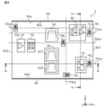
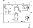
- FIG. 2 is a plan view of the high frequency module according to the first embodiment.
- FIG. 3 is a cross-sectional view of the high frequency module according to the first embodiment.
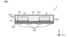
- FIG. 4 is a cross-sectional view of the high frequency module according to the first embodiment.
- FIG. 5 is a diagram showing a method of manufacturing a high frequency module according to the first embodiment.
- FIG. 6 is a plan view of the high frequency module according to the second embodiment.
- FIG. 7 is a plan view of the high frequency module according to the third embodiment.
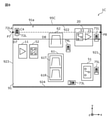
- FIG. 8 is a plan view of the high frequency module according to the fourth embodiment.
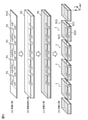
- FIG. 9 is a perspective view of the assembly board for the high frequency module according to the third and fourth embodiments.
- FIG. 10 is a plan view of the high frequency module according to another embodiment.
- each figure is a schematic diagram in which emphasis, omission, or ratio is adjusted as appropriate to show the present invention, and is not necessarily exactly illustrated. What is the actual shape, positional relationship, and ratio? May be different. In each figure, substantially the same configuration is designated by the same reference numeral, and duplicate description may be omitted or simplified.
- the x-axis and the y-axis are axes orthogonal to each other on a plane parallel to the main surface of the module substrate.
- the x-axis is parallel to the first side of the module substrate and the y-axis is parallel to the second side orthogonal to the first side of the module substrate.
- the z-axis is an axis perpendicular to the main surface of the module substrate, the positive direction thereof indicates an upward direction, and the negative direction thereof indicates a downward direction.
- connection includes not only the case of being directly connected by a connection terminal and / or a wiring conductor, but also the case of being electrically connected via another circuit element. Further, “connected between A and B” means that both A and B are connected between A and B.
- planar view means that an object is projected orthographically projected onto the xy plane from the positive side of the z-axis.
- distance between A and B means the length of a line segment connecting the representative point in A and the representative point in B.
- the representative point the center point of the object or the point closest to the other object can be used, but the present invention is not limited to this.
- terms that indicate relationships between elements such as “parallel” and “vertical”, terms that indicate the shape of elements such as “rectangle”, and numerical ranges do not mean only strict meanings. It means that a substantially equivalent range, for example, an error of about several percent is included.
- the component is laminated on another component arranged on the substrate), and a part or all of the component is embedded and arranged in the substrate.
- the component is arranged on the main surface of the board means that the component is arranged on the main surface in a state of being in contact with the main surface of the board, and the component is mainly arranged without contacting the main surface. This includes arranging above the surface and embedding a part of the component in the substrate from the main surface side.
- FIG. 1 is a circuit configuration diagram of a high frequency module 1 and a communication device 5 according to the first embodiment.
- the communication device 5 includes a high frequency module 1, an antenna 2, an RFIC 3, and a BBIC 4.
- the high frequency module 1 transmits a high frequency signal between the antenna 2 and the RFIC 3.
- the internal configuration of the high frequency module 1 will be described later.
- the antenna 2 is connected to the antenna connection terminal 101 of the high frequency module 1, transmits the high frequency signal output from the high frequency module 1, and also receives the high frequency signal from the outside and outputs it to the high frequency module 1.
- the BBIC 4 is a baseband signal processing circuit that processes signals using an intermediate frequency band having a lower frequency than the high frequency signal transmitted by the high frequency module 1.
- the signal processed by the BBIC 4 for example, an image signal for displaying an image and / or an audio signal for a call via a speaker are used.
- the antenna 2 and the BBIC 4 are not essential components. That is, the communication device 5 does not have to include the antenna 2 and the BBIC 4.
- the high frequency module 1 includes a power amplifier 11, a low noise amplifier 21, switches 51 to 53, a duplexer 61, a transmission / reception filter 62, a matching circuit (MN) 71 to 75, and an antenna connection. It includes a terminal 101, a high frequency input terminal 111, and a high frequency output terminal 121.
- MN matching circuit
- the antenna connection terminal 101 is connected to the antenna 2.
- the high frequency input terminal 111 is a terminal for receiving a high frequency transmission signal from the outside of the high frequency module 1.
- the high frequency input terminal 111 is a terminal for receiving transmission signals of communication bands A and B from RFIC3.
- the high frequency output terminal 121 is a terminal for providing a high frequency reception signal to the outside of the high frequency module 1.
- the high frequency output terminal 121 is a terminal for providing the reception signals of the communication bands A and B to the RFIC3.
- the communication band means a frequency band defined in advance by a standardization body or the like (for example, 3GPP (3rd Generation Partnership Project) and IEEE (Institute of Electrical and Electronics Engineers), etc.) for a communication system.
- a standardization body or the like for example, 3GPP (3rd Generation Partnership Project) and IEEE (Institute of Electrical and Electronics Engineers), etc.
- the communication system means a communication system constructed by using radio access technology (RAT: RadioAccess Technology).
- RAT RadioAccess Technology
- the communication system for example, a 5GNR (5th Generation New Radio) system, an LTE (Long Term Evolution) system, a WLAN (Wireless Local Area Network) system, or the like can be used, but the communication system is not limited thereto.
- the communication band A a communication band for frequency division duplex (FDD: Frequency Division Duplex) is used.
- FDD Frequency Division Duplex
- bands 1, 3, 25, 66 and the like for LTE and / or 5G NR can be used, but the communication band A is not limited thereto.
- the communication band B a communication band for time division duplex (TDD: Time Division Duplex) is used.
- TDD Time Division Duplex
- bands 34, 39 and the like for LTE and / or 5GNR can be used, but the communication band B is not limited to these.
- the power amplifier 11 can amplify the transmission signals of the communication bands A and B received by the high frequency input terminal 111.
- the input of the power amplifier 11 is connected to the high frequency input terminal 111, and the output of the power amplifier 11 is connected to the switch 52 via the matching circuit 72.
- the low noise amplifier 21 can amplify the received signals of the communication bands A and B.
- the input of the low noise amplifier is connected to the switch 53 via the matching circuit 71, and the output of the low noise amplifier 21 is connected to the high frequency output terminal 121.
- the configurations of the power amplifier 11 and the low noise amplifier 21 are not particularly limited.
- the power amplifier 11 and / or the low noise amplifier 21 may have a single-stage configuration or a multi-stage configuration.
- the power amplifier 11 and / or the low noise amplifier 21 may be a differential amplifier that converts a high frequency signal into a differential signal (that is, a complementary signal) and amplifies it.
- the duplexer 61 passes the high frequency signal of the communication band A.
- the duplexer 61 transmits the transmission signal and the reception signal of the communication band A by the FDD method.
- the duplexer 61 includes a transmit filter 61T and a receive filter 61R.
- the transmission filter 61T (A-Tx) is an example of the second filter and the third filter, and has a pass band including the uplink operating band of the communication band A.
- One end of the transmission filter 61T is connected to the antenna connection terminal 101 via the matching circuit 73, the switch 51, and the matching circuit 75.
- the other end of the transmission filter 61T is connected to the output of the power amplifier 11 via the switch 52.
- the uplink operation band means a part of the communication band and designated for the uplink.
- the uplink operation band means the transmission band.
- the reception filter 61R (A-Rx) is an example of the first filter and the third filter, and has a pass band including the downlink operating band of the communication band A.
- One end of the reception filter 61R is connected to the antenna connection terminal 101 via the matching circuit 73, the switch 51, and the matching circuit 75.
- the other end of the receive filter 61R is connected to the input of the low noise amplifier 21 via the switch 53.
- the downlink operation band means a part of the communication band and designated for the downlink.
- the downlink operation band means the reception band.
- the transmission / reception filter 62 (B-TRx) is an example of a first filter, a second filter, and a third filter, and has a pass band including a communication band B.
- One end of the transmission / reception filter 62 is connected to the antenna connection terminal 101 via the matching circuit 74, the switch 51, and the matching circuit 75.
- the other end of the transmit / receive filter 62 is connected to the output of the power amplifier 11 via the switch 52 and the matching circuit 72, and to the input of the low noise amplifier 21 via the switches 52 and 53 and the matching circuit 71.
- the switch 51 is connected between the antenna connection terminal 101 and the duplexer 61 and the transmission / reception filter 62.
- the switch 51 has terminals 511 to 513.
- the terminal 511 is connected to the antenna connection terminal 101 via the matching circuit 75.
- the terminal 512 is connected to the duplexer 61 via the matching circuit 73.
- the terminal 513 is connected to the transmission / reception filter 62 via the matching circuit 74.
- the switch 51 can connect the terminal 511 to at least one of the terminals 512 and 513, for example, based on the control signal from the RFIC3. That is, the switch 51 can switch the connection and disconnection between the antenna 2 and the duplexer 61, and can switch the connection and disconnection between the antenna 2 and the transmission / reception filter 62.
- the switch 51 is composed of, for example, a multi-connection type switch circuit, and may be called an antenna switch.
- the switch 52 is connected between the transmission filter 61T and the transmission / reception filter 62 and the power amplifier 11 and the low noise amplifier 21.
- the switch 52 has terminals 521 to 524.
- the terminals 521 and 522 are connected to the transmission filter 61T and the transmission / reception filter 62, respectively.
- the terminal 523 is connected to the output of the power amplifier 11 via the matching circuit 72.
- the terminal 524 is connected to the terminal 532 of the switch 53 and is connected to the input of the low noise amplifier 21 via the switch 53 and the matching circuit 71.
- the switch 52 can connect the terminal 521 to the terminal 523 and the terminal 522 to any of the terminals 523 and 524, for example, based on the control signal from the RFIC3. That is, the switch 52 can switch between connection and non-connection between the transmission filter 61T and the power amplifier 11, and can connect the transmission / reception filter 62 to either the power amplifier 11 or the low noise amplifier 21.
- the switch 52 is composed of, for example, a multi-connection type switch circuit.
- the switch 53 is connected between the reception filter 61R and the transmission / reception filter 62 and the low noise amplifier 21.
- the switch 53 has terminals 531 to 533. Terminal 531 is connected to the input of the low noise amplifier 21 via the matching circuit 71.
- the terminal 532 is connected to the terminal 524 of the switch 52, and is connected to the transmission / reception filter 62 via the switch 52.
- the terminal 533 is connected to the reception filter 61R.
- the switch 53 can connect terminals 532 and / or 533 to terminal 531 based on, for example, a control signal from RFIC3. That is, the switch 53 can switch the connection and non-connection between the reception filter 61R and the low noise amplifier 21, and can switch the connection and non-connection between the transmission / reception filter 62 and the low noise amplifier 21.
- the switch 53 is composed of, for example, a multi-connection type switch circuit.
- the matching circuit 71 is connected between the reception filter 61R and the transmission / reception filter 62 and the low noise amplifier 21. Specifically, the matching circuit 71 is connected between the switch 53 and the input of the low noise amplifier 21. The matching circuit 71 can achieve impedance matching between the low noise amplifier 21, the reception filter 61R, and the transmission / reception filter 62.
- the matching circuit 71 includes an inductor 71L, and may further include a capacitor.
- the matching circuit 72 is connected between the transmission filter 61T and the transmission / reception filter 62 and the power amplifier 11. Specifically, the matching circuit 72 is connected between the switch 52 and the input of the power amplifier 11. The matching circuit 72 can achieve impedance matching between the power amplifier 11, the transmission filter 61T, and the transmission / reception filter 62.
- the matching circuit 72 includes an inductor 72L and may further include a capacitor.
- the matching circuit 73 is connected between the duplexer 61 and the antenna connection terminal 101. Specifically, the matching circuit 73 is connected between the duplexer 61 and the switch 51. The matching circuit 73 can achieve impedance matching between the duplexer 61 and the antenna 2.
- the matching circuit 73 includes an inductor 73L and may further include a capacitor.
- the matching circuit 74 is connected between the transmission / reception filter 62 and the antenna connection terminal 101. Specifically, the matching circuit 74 is connected between the transmission / reception filter 62 and the switch 51. The matching circuit 74 can achieve impedance matching between the transmission / reception filter 62 and the antenna 2.
- the matching circuit 74 includes an inductor 74L and may further include a capacitor.
- the matching circuit 75 is connected between the duplexer 61 and the transmission / reception filter 62 and the antenna connection terminal 101. Specifically, the matching circuit 75 is connected between the switch 51 and the antenna connection terminal 101. The matching circuit 75 can achieve impedance matching between the duplexer 61 and the transmit / receive filter 62 and the antenna 2.
- the matching circuit 75 includes an inductor 75L and may further include a capacitor.
- the high frequency module 1 may include at least two of a power amplifier 11, a low noise amplifier 21, switches 51 to 53, a duplexer 61, a transmission / reception filter 62, and an inductor 71L to 75L.
- FIG. 2 is a plan view of the high frequency module 1 according to the first embodiment. Specifically, FIG. 2 shows a view of the main surface 91a of the module substrate 91 from the positive side of the z-axis.
- FIGS. 3 and 4 is a cross-sectional view of the high frequency module 1 according to the first embodiment.
- the cross sections of the high frequency module 1 in FIGS. 3 and 4 are the cross sections of the iii-iii line and the iv-iv line of FIG. 2, respectively.
- the high frequency module 1 further includes a module substrate 91, a resin member 92, and a shield electrode layer. It includes 95 and a plurality of external connection terminals 150.
- the illustration of the resin member 92 and the top surface of the shield electrode layer 95 is omitted.
- the module board 91 has main surfaces 91a and 91b facing each other.
- the module substrate 91 has a rectangular shape in a plan view, but the shape of the module substrate 91 is not limited to the rectangular shape.
- the module substrate 91 include a low-temperature co-fired ceramics (LTCC: Low Temperature Co-fired Ceramics) substrate having a laminated structure of a plurality of dielectric layers, a high-temperature co-fired ceramics (HTCC: High Temperature Co-fired Ceramics) substrate, and the like.
- LTCC Low Temperature Co-fired Ceramics
- HTCC High Temperature Co-fired Ceramics
- a board having a built-in component, a board having a redistribution layer (RDL: Redistribution Layer), a printed circuit board, or the like can be used, but is not limited thereto.
- RDL Redistribution Layer
- the main surface 91a is an example of the first main surface.
- a plurality of high-frequency components and a resin member 92 are arranged on the main surface 91a.
- the plurality of high frequency components include a power amplifier 11, a low noise amplifier 21, switches 51 to 53, a duplexer 61, a transmission / reception filter 62, and an inductor 71L to 75L.
- the main surface 91b is an example of the second main surface.
- a plurality of external connection terminals 150 are arranged on the main surface 91b.
- the resin member 92 is arranged on the main surface 91a of the module substrate 91 and covers the main surface 91a and the parts on the main surface 91a.
- the resin member 92 has a function of ensuring reliability such as mechanical strength and moisture resistance of the parts on the main surface 91a.
- the resin member 92 is formed into a rectangular parallelepiped shape on the main surface 91a. Specifically, the resin member 92 has four side surfaces 921 to 924 along the outer edge (that is, four sides) of the module substrate 91, and has a top surface 925 above the main surface 91a of the module substrate 91.
- Side surfaces 921 and 923 are examples of the first side surface and the third side surface.
- the side surfaces 921 and 923 are along the short side of the module board 91 and face each other.
- the side surfaces 922 and 924 are examples of the second side surface and the fourth side surface.
- the side surfaces 922 and 924 are along the long side of the module board 91 and face each other.
- the shield electrode layer 95 is a metal film formed by, for example, a sputtering method, and covers the top surface 925 and the side surfaces 922 and 924 of the resin member 92.
- the shield electrode layer 95 is set to the ground potential and suppresses external noise from invading the components constituting the high frequency module 1.
- the shield electrode layer 95 covers the side surfaces 922 and 924 of the four side surfaces 921 to 924 of the resin member 92 without covering the side surfaces 921 and 923. In other words, the shield electrode layer 95 covers only two side surfaces 922 and 924 facing each other among the four side surfaces 921 to 924 of the resin member 92.
- the low noise amplifier 21 and the switch 53 are built in one semiconductor integrated circuit 20.
- the semiconductor integrated circuit 20 is an electronic component having an electronic circuit formed on the surface and inside of a semiconductor chip (also referred to as a die).
- the semiconductor integrated circuit 20 has a rectangular shape in a plan view. The shape of the semiconductor integrated circuit 20 is not limited to a rectangle.
- the circuit elements built in the semiconductor integrated circuit 20 are not limited to the low noise amplifier 21 and the switch 53.
- the switch 51 may be built in the semiconductor integrated circuit 20.
- the semiconductor integrated circuit 20 is composed of, for example, CMOS (Complementary Metal Oxide Semiconductor), and may be specifically configured by an SOI (Silicon on Insulator) process. This makes it possible to manufacture the semiconductor integrated circuit 20 at low cost.
- the semiconductor integrated circuit 20 may be composed of at least one of GaAs, SiGe, and GaN. This makes it possible to realize a high-quality semiconductor integrated circuit 20.
- Each of the transmission filter 61T, the reception filter 61R, and the transmission / reception filter 62 may be, for example, any of an elastic surface wave filter, an elastic wave filter using a BAW (Bulk Acoustic Wave), an LC resonance filter, and a dielectric filter. , And further, not limited to these.
- Each of the inductors 71L to 75L is composed of a coil, and is mounted as, for example, a surface mount device (SMD: Surface Mount Device).
- SMD Surface Mount Device
- the inductors 71L to 75L do not have to be SMD, and may be formed in the module substrate 91.
- the inductor 71L is an example of the first inductor and is arranged in the vicinity of the side surface 921 of the resin member 92. Specifically, the inductor 71L is closer to the side surface 921 of the side surfaces 921 and 922. Further, the inductor 71L is closer to the side surface 921 than the low noise amplifier 21.
- the winding shaft 71La of the coil constituting the inductor 71L is parallel to the side surfaces 922 and 924 and perpendicular to the side surfaces 921 and 923. That is, the winding shaft 71La intersects the side surfaces 921 and 923, but does not intersect the side surfaces 922 and 924, so that it does not intersect the shield electrode layer 95.
- the inductor 72L is an example of the second inductor, and is arranged in the vicinity of the side surface 923 of the resin member 92. Specifically, the inductor 72L is closer to the side surface 923 of the side surface 923 and 922. Further, the inductor 72L is closer to the side surface 923 than the power amplifier 11.
- the winding shaft 72La of the coil constituting the inductor 72L is parallel to the side surfaces 922 and 924 and perpendicular to the side surfaces 921 and 923. That is, the winding shaft 72La intersects the side surfaces 921 and 923, but does not intersect the side surfaces 922 and 924, so that it does not intersect the shield electrode layer 95.
- the inductor 73L is arranged in the vicinity of the side surface 924 of the resin member 92.
- the winding shaft 73La of the coil constituting the inductor 73L does not intersect the side surfaces 921 and 923 of the resin member 92, but intersects the side surfaces 922 and 924 of the resin member 92.
- the inductor 74L is an example of the third inductor and is arranged near the center of the module board 91.
- the winding shaft 74La of the coil constituting the inductor 74L is parallel to the side surfaces 922 and 924 and perpendicular to the side surfaces 921 and 923. That is, the winding shaft 74La intersects the side surfaces 921 and 923, but does not intersect the side surfaces 922 and 924, so that it does not intersect the shield electrode layer 95.
- the inductor 75L is an example of the third inductor, and is arranged in the vicinity of the side surface 921 of the resin member 92. Specifically, the inductor 75L is closer to the side surface 921 of the side surfaces 921 and 924. Further, the inductor 75L is closer to the side surface 921 than the duplexer 61 and the transmission / reception filter 62.
- the winding shaft 75La of the coil constituting the inductor 75L is parallel to the side surfaces 922 and 924 and perpendicular to the side surfaces 921 and 923. That is, the winding shaft 75La intersects the side surfaces 921 and 923, but does not intersect the side surfaces 922 and 924, so that it does not intersect the shield electrode layer 95.
- the plurality of external connection terminals 150 include the antenna connection terminal 101, the high frequency input terminal 111, and the high frequency output terminal 121 shown in FIG. Each of the plurality of external connection terminals 150 is connected to an input / output terminal and / or a ground terminal or the like on the mother board arranged in the negative direction of the z-axis of the high frequency module 1. Pad electrodes can be used as the plurality of external connection terminals 150, but the present invention is not limited to this.
- FIG. 5 is a diagram showing a method of manufacturing the high frequency module 1 according to the first embodiment.
- an assembly board 910 on which a plurality of high-frequency components are mounted is prepared.
- the assembly board 910 includes a plurality of module boards 91, and is an aggregate of the plurality of module boards 91. In FIG. 5, the plurality of module boards 91 are arranged in a row in the collective board 910.
- the resin member 92 is molded so as to cover the main surface of the assembly substrate 910 and a plurality of high-frequency components on the main surface.
- the resin member 92 is formed by pouring the resin into a mold installed on the assembly substrate 910 and then solidifying the resin.
- the surface of the molded resin member 92 is polished or ground as needed.
- (C) Film formation step Next, a metal film is formed as a shield electrode layer 95 on the surface of the resin member 92 that covers the assembly substrate 910. That is, the shield electrode layers 95 of the plurality of high frequency modules 1 are integrally molded.
- the method for forming the metal film is not particularly limited, but for example, a sputtering method or the like can be used.
- the high-frequency module 1 includes a module substrate 91 having main surfaces 91a and 91b facing each other, a plurality of high-frequency components arranged on at least one of the main surfaces 91a and 91b, and a main component.
- a resin member 92 covering at least one of the surfaces 91a and 91b and having a plurality of side surfaces including side surfaces 921 and / or 923 and side surfaces 922 and / or 924 along the outer edge of the module substrate 91, and side surfaces 921 and /.
- the shield electrode layer 95 is provided, which does not cover the 923 but covers the side surface 922 and / or the 924.
- the side surface 922 and / or 924 can be covered with the shield electrode layer 95 without covering the side surface 921 and / or 923 with the shield electrode layer 95.
- the high frequency component may be magnetically coupled, electrocoupled or electromagnetically coupled to other high frequency components via the shielded electrode layer 95. Therefore, by not covering the side surface 921 and / or 923 of the plurality of side surfaces with the shield electrode layer 95, such coupling can be suppressed and the isolation between the plurality of high frequency components can be improved. .. Further, by covering the side surface 922 and / or 924 of the plurality of side surfaces with the shield electrode layer 95, it is possible to suppress the invasion of external noise into the high frequency component.
- the plurality of high frequency components are matched with the receiving filter 61R, the low noise amplifier 21, and the inductor 71L connected between the receiving filter 61R and the low noise amplifier 21.
- the circuit 71 may be included, and the inductor 71L may be closer to the side surface 921 of the side surfaces 921 and 922.
- the inductor 71L can be arranged closer to the side surface 921 not covered with the shield electrode layer 95 than to the side surface 922 covered with the shield electrode layer 95.
- the inductor is easily coupled to other high frequency components, so that coupling between a plurality of high frequency components via the shield electrode layer 95 can be suppressed more effectively.
- the inductor 71L is arranged in the reception path, it is possible to suppress a decrease in reception sensitivity by suppressing coupling between the inductor 71L and other high-frequency components.
- the plurality of high frequency components are matched with the receiving filter 61R, the low noise amplifier 21, and the inductor 71L connected between the receiving filter 61R and the low noise amplifier 21.
- the circuit 71 may be included, and the inductor 71L may be closer to the side surface 921 than the low noise amplifier 21.
- the inductor 71L can be arranged closer to the side surface 921 not covered with the shield electrode layer 95 than the low noise amplifier 21.
- the inductor is easily coupled to other high frequency components, so that coupling between a plurality of high frequency components via the shield electrode layer 95 can be suppressed more effectively.
- the inductor 71L is arranged in the reception path, it is possible to suppress a decrease in reception sensitivity by suppressing coupling between the inductor 71L and other high-frequency components.
- the plurality of high frequency components are matched with the receiving filter 61R, the low noise amplifier 21, and the inductor 71L connected between the receiving filter 61R and the low noise amplifier 21.
- the circuit 71 may be included, and the winding shaft 71La of the coil constituting the inductor 71L may or may not intersect the side surface 921 and may not intersect the side surface 922.
- the inductor 71L can be arranged so that the winding shaft 71La of the coil constituting the inductor 71L does not intersect the side surface 922 covered with the shield electrode layer 95.
- inductors generate a strong magnetic force along the winding axis of the coil and are prone to magnetic field coupling with components on the winding axis. Therefore, by preventing the winding shaft 71La from intersecting the side surface 922 covered with the shield electrode layer 95, it is possible to effectively suppress magnetic field coupling of the inductor 71L with other high frequency components via the shield electrode layer 95. can.
- the inductor 71L is arranged in the reception path, it is possible to suppress a decrease in reception sensitivity by suppressing coupling between the inductor 71L and other high-frequency components.
- the plurality of high frequency components may include a transmission filter 61T, a power amplifier 11, and an inductor 72L connected between the transmission filter 61T and the power amplifier 11.
- the inductor 72L may be closer to the side surface 923 of the side surfaces 922 and 923.
- the inductor 72L can be arranged closer to the side surface 923 not covered with the shield electrode layer 95 than to the side surface 922 covered with the shield electrode layer 95.
- the inductor is easily coupled to other high frequency components, so that coupling between a plurality of high frequency components via the shield electrode layer 95 can be suppressed more effectively.
- the inductor 72L is arranged in the transmission path, it is possible to suppress deterioration of the quality of the transmission signal by suppressing the coupling between the inductor 72L and other high frequency components.
- the plurality of high frequency components may include a transmission filter 61T, a power amplifier 11, and an inductor 72L connected between the transmission filter 61T and the power amplifier 11.
- the inductor 72L may be closer to the side surface 923 than the power amplifier 11.
- the inductor 72L can be arranged closer to the side surface 923 not covered with the shield electrode layer 95 than the power amplifier 11.
- the inductor is easily coupled to other high frequency components, so that coupling between a plurality of high frequency components via the shield electrode layer 95 can be suppressed more effectively.
- the inductor 72L is arranged in the transmission path, it is possible to suppress deterioration of the quality of the transmission signal by suppressing the coupling between the inductor 72L and other high frequency components.
- the plurality of high frequency components may include a transmission filter 61T, a power amplifier 11, and an inductor 72L connected between the transmission filter 61T and the power amplifier 11.
- the winding shaft 72La of the coil constituting the inductor 72L may or may not intersect the side surface 922.
- the inductor 72L can be arranged so that the winding shaft 72La of the coil constituting the inductor 72L does not intersect the side surface 922 covered with the shield electrode layer 95.
- inductors generate a strong magnetic force along the winding axis of the coil and are prone to magnetic field coupling with components on the winding axis. Therefore, by preventing the winding shaft 72La from intersecting the side surface 922 covered with the shield electrode layer 95, it is possible to effectively suppress magnetic field coupling of the inductor 72L with other high frequency components via the shield electrode layer 95. can.
- the inductor 72L is arranged in the transmission path, it is possible to suppress deterioration of the quality of the transmission signal by suppressing the coupling between the inductor 72L and other high frequency components.
- the plurality of high frequency components may include a transmission / reception filter 62 and an inductor 75L connected between the transmission / reception filter 62 and the antenna connection terminal 101, and the inductor 75L may be included. May be closer to the side surface 921 of the side surfaces 921 and 924.
- the inductor 75L can be arranged closer to the side surface 921 not covered with the shield electrode layer 95 than to the side surface 924 covered with the shield electrode layer 95.
- the inductor is easily coupled to other high frequency components, so that coupling between a plurality of high frequency components via the shield electrode layer 95 can be suppressed more effectively.
- the inductor 75L is arranged in the transmission / reception path, it is possible to suppress deterioration of transmission signal quality and reception sensitivity by suppressing coupling between the inductor 75L and other high-frequency components. ..
- the plurality of high frequency components may include a transmission / reception filter 62 and an inductor 75L connected between the transmission / reception filter 62 and the antenna connection terminal 101, and the transmission / reception filter may be included.
- the inductor 75L may be closer to the side surface 921 than the inductor 62.
- the inductor 75L can be arranged closer to the side surface 921 not covered with the shield electrode layer 95 than the transmission / reception filter 62.
- the inductor is easily coupled to other high frequency components, so that coupling between a plurality of high frequency components via the shield electrode layer 95 can be suppressed more effectively.
- the inductor 75L is arranged in the transmission / reception path, it is possible to suppress deterioration of transmission signal quality and reception sensitivity by suppressing coupling between the inductor 75L and other high-frequency components. ..
- the plurality of high frequency components may include a transmission / reception filter 62 and an inductor 74L and / or 75L connected between the transmission / reception filter 62 and the antenna connection terminal 101.
- the winding shaft 74La of the coil constituting the inductor 74L and / or the winding shaft 75La of the coil constituting the inductor 75L may or may not intersect the side surface 921.
- the inductor 74L and / or the inductor 74L so that the winding shaft 74La of the coil constituting the inductor 74L and / or the winding shaft 75La of the coil constituting the inductor 75L do not intersect the side surface 924 covered with the shield electrode layer 95.
- 75 L can be arranged.
- inductors generate a strong magnetic force along the winding axis of the coil and are prone to magnetic field coupling with components on the winding axis.
- the inductor 74L and / or 75L is magnetically coupled to other high frequency components via the shield electrode layer 95. Can be effectively suppressed. Further, since the inductor 75L is arranged in the transmission / reception path, it is possible to suppress deterioration of transmission signal quality and reception sensitivity by suppressing coupling between the inductor 75L and other high-frequency components. ..
- the plurality of side surfaces include the side surfaces 921 to 924, and the shield electrode layer 95 does not cover the side surfaces 921 and 923 but covers the side surfaces 922 and the side surface 924. good.
- two side surfaces 921 and 923 not covered with the shield electrode layer 95 and two side surfaces 922 and 924 covered with the shield electrode layer 95 can be arranged, respectively. Therefore, it is possible to balance the suppression of coupling between high-frequency components and the suppression of intrusion of external noise.
- the side surfaces 921 and 923 may face each other, and the side surfaces 922 and 924 may face each other.
- the side surfaces 921 and 923 not covered by the shield electrode layer 95 can be opposed to each other, and the side surfaces 922 and 924 covered by the shield electrode layer 95 can be opposed to each other. Therefore, it is easy to arrange the inductor so that the winding shaft does not intersect the side surface covered with the shield electrode layer 95, and it is easier to arrange a plurality of high frequency components rather than suppressing the coupling between the high frequency components. Become.
- the communication device 5 includes an RFIC 3 for processing a high frequency signal and a high frequency module 1 for transmitting a high frequency signal between the RFIC 3 and the antenna 2.
- the same effect as that of the high frequency module 1 can be realized.
- the manufacturing method of the high frequency module 1 is a manufacturing method for manufacturing a plurality of high frequency modules 1, and is mainly a collective board 910 having a plurality of module boards 91 in which a plurality of high frequency components are arranged.
- a resin molding step of molding the resin member 92 covering the surface, a film forming step of forming a metal film as a shield electrode layer 95 on the surface of the molded resin member 92, and an assembly substrate 910 after the shield electrode layer 95 is formed. Includes a cutting step of manufacturing a plurality of high frequency modules 1 by cutting.
- the shield electrode layer 95 can be collectively formed by the plurality of high frequency modules 1 before cutting the assembly substrate 910. Therefore, the plurality of high frequency modules 1 can be manufactured more easily than the case where the shield electrode layer 95 is individually formed by the plurality of high frequency modules 1. Further, the shield electrode layer 95 is not formed on the cut surface of the plurality of high frequency modules 1 manufactured in this way. Therefore, the plurality of high frequency modules 1 manufactured in this way can suppress the coupling between the plurality of high frequency components via the shield electrode layer 95.
- circuit configuration of the high frequency module 1A according to the present embodiment is the same as that of the high frequency module 1 according to the first embodiment, illustration and description thereof will be omitted.
- FIG. 6 is a plan view of the high frequency module 1A according to the second embodiment.
- the side surfaces 922 and 924 of the resin member 92 correspond to the first side surface and the third side surface
- the side surfaces 921 and 923 correspond to the second side surface and the fourth side surface.
- the shield electrode layer 95A does not cover the side surfaces 922 and 924 of the four side surfaces 921 to 924 of the resin member 92, but covers the side surfaces 921 and 923. In other words, the shield electrode layer 95A covers only two side surfaces 921 and 923 facing each other among the four side surfaces 921 to 924 of the resin member 92.
- the inductor 71L is an example of the first inductor and is arranged in the vicinity of the side surface 922 of the resin member 92. Specifically, the inductor 71L is closer to the side surface 922 of the side surfaces 921 and 922. Further, the inductor 71L is closer to the side surface 922 than the low noise amplifier 21.
- the winding shaft 71La of the coil constituting the inductor 71L is parallel to the side surfaces 921 and 923 and perpendicular to the side surfaces 922 and 924. That is, the winding shaft 71La intersects the side surfaces 922 and 924, but does not intersect the side surfaces 921 and 923, so that it does not intersect the shield electrode layer 95.
- the inductor 73L is an example of the third inductor, and is arranged in the vicinity of the side surface 924 of the resin member 92. Specifically, the inductor 73L is closer to the side surface 924 of the side surfaces 921 and 924. Further, the inductor 73L is closer to the side surface 924 than the duplexer 61 and the transmission / reception filter 62.
- the winding shaft 73La of the coil constituting the inductor 73L is parallel to the side surfaces 921 and 923 and perpendicular to the side surfaces 922 and 924. That is, the winding shaft 73La intersects the side surfaces 922 and 924, but does not intersect the side surfaces 921 and 923, so that it does not intersect the shield electrode layer 95.
- the high-frequency module 1A includes a module substrate 91 having main surfaces 91a and 91b facing each other, a plurality of high-frequency components arranged on at least one of the main surfaces 91a and 91b, and a main component.
- a resin member 92 that covers at least one of the surfaces 91a and 91b and has a plurality of side surfaces including side surfaces 921 and / or 923 and side surfaces 922 and / or 924 along the outer edge of the module substrate 91, and side surfaces 922 and /.
- the shield electrode layer 95A covering the side surface 921 and / or 923 without covering the 924 is provided.
- the side surface 921 and / or 923 can be covered with the shield electrode layer 95A without covering the side surface 922 and / or 924 with the shield electrode layer 95A.
- the high frequency component may be magnetically coupled, electrocoupled or electromagnetically coupled to other high frequency components via the shielded electrode layer 95A. Therefore, by not covering the side surface 922 and / or 924 of the plurality of side surfaces with the shield electrode layer 95A, such coupling can be suppressed and the isolation between the plurality of high frequency components can be improved. .. Further, by covering the side surface 921 and / or 923 of the plurality of side surfaces with the shield electrode layer 95A, it is possible to suppress the invasion of external noise into the high frequency component.
- the plurality of high frequency components include a receiving filter 61R, a low noise amplifier 21, and an inductor 71L connected between the receiving filter 61R and the low noise amplifier 21.
- the inductor 71L may be included, and the inductor 71L may be closer to the side surface 922 of the side surfaces 921 and 922.
- the inductor 71L can be arranged closer to the side surface 922 not covered with the shield electrode layer 95A than to the side surface 921 covered with the shield electrode layer 95A.
- the inductor is easily coupled to other high frequency components, so that coupling between a plurality of high frequency components via the shield electrode layer 95A can be suppressed more effectively.
- the inductor 71L is arranged in the reception path, it is possible to suppress a decrease in reception sensitivity by suppressing coupling between the inductor 71L and other high-frequency components.
- the plurality of high frequency components include a receiving filter 61R, a low noise amplifier 21, and an inductor 71L connected between the receiving filter 61R and the low noise amplifier 21. It may be included, and the inductor 71L may be closer to the side surface 922 than the low noise amplifier 21.
- the inductor 71L can be arranged closer to the side surface 922 not covered with the shield electrode layer 95A than the low noise amplifier 21.
- the inductor is easily coupled to other high frequency components, so that coupling between a plurality of high frequency components via the shield electrode layer 95A can be suppressed more effectively.
- the inductor 71L is arranged in the reception path, it is possible to suppress a decrease in reception sensitivity by suppressing coupling between the inductor 71L and other high-frequency components.
- the plurality of high frequency components include a receiving filter 61R, a low noise amplifier 21, and an inductor 71L connected between the receiving filter 61R and the low noise amplifier 21. It may be included, and the winding shaft 71La of the coil constituting the inductor 71L may or may not intersect the side surface 922 or may not intersect the side surface 921.
- the inductor 71L can be arranged so that the winding shaft 71La of the coil constituting the inductor 71L does not intersect the side surface 921 covered with the shield electrode layer 95A.
- inductors generate a strong magnetic force along the winding axis of the coil and are prone to magnetic field coupling with components on the winding axis. Therefore, by preventing the winding shaft 71La from intersecting the side surface 921 covered with the shield electrode layer 95A, it is possible to effectively suppress the inductor 71L from magnetic field coupling with other high frequency components via the shield electrode layer 95A. can. Further, since the inductor 71L is arranged in the reception path, it is possible to suppress a decrease in reception sensitivity by suppressing coupling between the inductor 71L and other high-frequency components.
- the plurality of high frequency components may include a duplexer 61 and an inductor 73L connected between the duplexer 61 and the antenna connection terminal 101, and the inductor 73L may include the inductor 73L.
- the side surface 924 may be closer.
- the inductor 73L can be arranged closer to the side surface 924 not covered with the shield electrode layer 95A than to the side surface 921 covered with the shield electrode layer 95A.
- the inductor is easily coupled to other high frequency components, so that coupling between a plurality of high frequency components via the shield electrode layer 95A can be suppressed more effectively.
- the inductor 73L is arranged in the transmission / reception path of the communication band A, the quality of the transmission signal of the communication band A is deteriorated and the communication band is deteriorated by suppressing the coupling between the inductor 73L and other high frequency components. It is possible to suppress a decrease in the reception sensitivity of A.
- the plurality of high frequency components may include the duplexer 61 and the inductor 73L connected between the duplexer 61 and the antenna connection terminal 101, and may be more than the duplexer 61.
- the inductor 73L may be closer to the side surface 924.
- the inductor 73L can be arranged closer to the side surface 924 not covered with the shield electrode layer 95A than the duplexer 61.
- the inductor is easily coupled to other high frequency components, so that coupling between a plurality of high frequency components via the shield electrode layer 95A can be suppressed more effectively.
- the inductor 73L is arranged in the transmission / reception path of the communication band A, the quality of the transmission signal of the communication band A is deteriorated and the communication band is deteriorated by suppressing the coupling between the inductor 73L and other high frequency components. It is possible to suppress a decrease in the reception sensitivity of A.
- the plurality of high frequency components may include a duplexer 61 and an inductor 73L connected between the duplexer 61 and the antenna connection terminal 101, and constitutes the inductor 73L.
- the winding shaft 73La of the coil may or may not intersect the side surface 924.
- the inductor 73L can be arranged so that the winding shaft 73La of the coil constituting the inductor 73L does not intersect the side surface 921 covered with the shield electrode layer 95A.
- inductors generate a strong magnetic force along the winding axis of the coil and are prone to magnetic field coupling with components on the winding axis. Therefore, by preventing the winding shaft 73La from intersecting the side surface 921 covered with the shield electrode layer 95A, it is possible to effectively suppress the inductor 73L from magnetic field coupling with other high frequency components via the shield electrode layer 95A. can.
- the inductor 73L is arranged in the transmission / reception path of the communication band A, the quality of the transmission signal of the communication band A is deteriorated and the communication band is deteriorated by suppressing the coupling between the inductor 73L and other high frequency components. It is possible to suppress a decrease in the reception sensitivity of A.
- circuit configuration of the high frequency module 1B according to the present embodiment is the same as that of the high frequency module 1 according to the first embodiment, illustration and description thereof will be omitted.
- the side surface 921 of the resin member 92 corresponds to the first side surface
- the side surfaces 922 to 924 correspond to the second side surface to the fourth side surface
- the shield electrode layer 95B does not cover the side surface 921 but covers the side surfaces 922 to 924 among the four side surfaces 921 to 924 of the resin member 92. In other words, the shield electrode layer 95B does not cover only one side surface 921 of the four side surfaces 921 to 924 of the resin member 92.
- the inductor 71L is an example of the first inductor and is arranged in the vicinity of the side surface 921 of the resin member 92.
- the winding shaft 71La of the coil constituting the inductor 71L is parallel to the side surfaces 922 and 924 and perpendicular to the side surfaces 921 and 923. That is, since the winding shaft 71La intersects the side surfaces 921 and 923, it also intersects with the shield electrode layer 95B covering the side surface 923.
- the distance D1 between the intersection P1 of the winding shaft 71La and the side surface 921 and the center point C1 of the inductor 71L is the distance between the intersection P2 of the winding shaft 71La and the side surface 923 and the center point C1 of the inductor 71L. Shorter than D2. That is, the distance D1 between the inductor 71L and the side surface 921 on the winding shaft 71La is shorter than the distance D2 between the inductor 71L and the side surface 923.
- the inductor 74L is an example of the third inductor and is arranged near the center of the module board 91.
- the winding shaft 74La of the coil constituting the inductor 74L is parallel to the side surfaces 922 and 924 and perpendicular to the side surfaces 921 and 923. That is, since the winding shaft 74La intersects the side surfaces 921 and 923, it also intersects with the shield electrode layer 95B covering the side surface 923.
- the distance D3 between the intersection P3 of the winding shaft 74La and the side surface 921 and the center point C2 of the inductor 74L is the distance between the intersection P4 of the winding shaft 74La and the side surface 923 and the center point C2 of the inductor 74L. Shorter than D4. That is, the distance D3 between the inductor 74L and the side surface 921 on the winding shaft 74La is shorter than the distance D4 between the inductor 74L and the side surface 923.
- the inductor 75L is an example of the third inductor, and is arranged in the vicinity of the side surface 921 of the resin member 92.
- the winding shaft 75La of the coil constituting the inductor 75L is parallel to the side surfaces 922 and 924 and perpendicular to the side surfaces 921 and 923. That is, since the winding shaft 75La intersects the side surfaces 921 and 923, it also intersects with the shield electrode layer 95B covering the side surface 923.
- the distance D5 between the intersection P5 of the winding shaft 75La and the side surface 921 and the center point C3 of the inductor 75L is the distance between the intersection P6 of the winding shaft 75La and the side surface 923 and the center point C3 of the inductor 75L. Shorter than D6. That is, the distance D5 between the inductor 75L and the side surface 921 on the winding shaft 75La is shorter than the distance D6 between the inductor 75L and the side surface 923.
- FIG. 9 is a perspective view of the assembly substrate 910BC for the high frequency modules 1B and 1C according to the third and fourth embodiments.
- an assembly board 910BC including two module boards 91 is prepared. Then, a resin molding step, a film forming step, and a cutting step are executed on the collective substrate 910BC. As a result, the assembly substrate 910BC is cut after the shield electrode layer is formed on the surface of the resin member on the assembly substrate 910BC. At this time, in the left module substrate 91 in the assembly substrate 910BC, the shield electrode layer 95B is formed on three side surfaces 922 to 924 of the four side surfaces 921 to 924 of the resin member 92, and the shield electrode layer 95B is formed on one side surface 921. Layer 95B is not formed. That is, the high frequency module 1B is manufactured.
- the high-frequency module 1B includes a module substrate 91 having main surfaces 91a and 91b facing each other, a plurality of high-frequency components arranged on at least one of the main surfaces 91a and 91b, and a main component. It covers at least one of the surfaces 91a and 91b, and covers the resin member 92 having a plurality of side surfaces including the side surfaces 921 to 924 along the outer edge of the module substrate 91, and the side surfaces 922 to 924 without covering the side surface 921.
- a shield electrode layer 95B and the like are provided.
- the side surfaces 922 to 924 can be covered with the shield electrode layer 95B without covering the side surface 921 with the shield electrode layer 95B.
- the high frequency component may be magnetically coupled, electrocoupled or electromagnetically coupled to other high frequency components via the shielded electrode layer 95B. Therefore, by not covering the side surface 921 of the plurality of side surfaces with the shield electrode layer 95B, such coupling can be suppressed and the isolation between the plurality of high frequency components can be improved. Further, by covering the side surfaces 922 to 924 of the plurality of side surfaces with the shield electrode layer 95B, it is possible to suppress the invasion of external noise into the high frequency component.
- the plurality of high frequency components include a receiving filter 61R, a low noise amplifier 21, and an inductor 71L connected between the receiving filter 61R and the low noise amplifier 21.
- D1 may be shorter than the distance D2 between the intersection P2 of the winding shaft 71La and the side surface 923 and the center point C1 of the inductor 71L.
- the winding shaft 71La of the inductor 71L intersects both the side surface 921 not covered by the shield electrode layer 95B and the side surface 923 covered by the shield electrode layer 95B, between the inductor 71L and the side surface 923.
- the distance D2 on the winding shaft 71La can be made longer than the distance D1 on the winding shaft 71La between the inductor 71L and the side surface 921. Therefore, it is possible to prevent the inductor 71L from coupling with other high frequency components via the shield electrode layer 95B covering the side surface 923.
- the plurality of high frequency components may include a transmission / reception filter 62 and an inductor 74L connected between the transmission / reception filter 62 and the antenna connection terminal 101.
- the winding shaft 74La of the coil constituting the 74L may intersect each of the side surfaces 921 and 923, and the distance D3 between the intersection P3 of the winding shaft 74La and the side surface 921 and the center point C2 of the inductor 74L is set. It may be shorter than the distance D4 between the intersection P4 of the winding shaft 74La and the side surface 923 and the center point C2 of the inductor 74L.
- the winding shaft 74La of the inductor 74L intersects both the side surface 921 not covered by the shield electrode layer 95B and the side surface 923 covered by the shield electrode layer 95B, between the inductor 74L and the side surface 923.
- the distance D4 on the winding shaft 74La can be made longer than the distance D3 on the winding shaft 74La between the inductor 74L and the side surface 921. Therefore, it is possible to prevent the inductor 74L from coupling with other high frequency components via the shield electrode layer 95B covering the side surface 923.
- the plurality of high frequency components may include a transmission / reception filter 62 and an inductor 75L connected between the transmission / reception filter 62 and the antenna connection terminal 101, and the inductor may be included.
- the winding shaft 75La of the coil constituting the 75L may intersect each of the side surfaces 921 and 923, and the distance D5 between the intersection P5 of the winding shaft 75La and the side surface 921 and the center point C3 of the inductor 75L is set. It may be shorter than the distance D6 between the intersection P6 of the winding shaft 75La and the side surface 923 and the center point C3 of the inductor 75L.
- the winding shaft 75La of the inductor 75L intersects both the side surface 921 not covered by the shield electrode layer 95B and the side surface 923 covered by the shield electrode layer 95B, between the inductor 75L and the side surface 923.
- the distance D6 on the winding shaft 75La can be made longer than the distance D5 on the winding shaft 75La between the inductor 75L and the side surface 921. Therefore, it is possible to prevent the inductor 75L from coupling with other high frequency components via the shield electrode layer 95B covering the side surface 923.
- the plurality of side surfaces may include the side surfaces 921 to 924, and the shield electrode layer 95B may cover the side surfaces 922 to 924 without covering the side surface 921.
- the high frequency module 1B suppresses the intrusion of external noise more than the high frequency module 1 or 1A according to the first or second embodiment. Can be strengthened.
- the present embodiment is mainly different from the first embodiment in that the three side surfaces of the resin member are covered with the shield electrode layer.
- the present embodiment will be described with reference to the drawings, focusing on the differences from the first embodiment.
- circuit configuration of the high frequency module 1C according to the present embodiment is the same as that of the high frequency module 1 according to the first embodiment, illustration and description thereof will be omitted.
- FIG. 8 is a plan view of the high frequency module 1C according to the fourth embodiment.
- the side surface 923 of the resin member 92 corresponds to the first side surface
- the side surfaces 921, 922 and 924 correspond to the second side surface to the fourth side surface.
- the shield electrode layer 95C covers the side surfaces 921, 922 and 924 of the four side surfaces 921 to 924 of the resin member 92 without covering the side surface 923. In other words, the shield electrode layer 95C does not cover only one side surface 923 of the four side surfaces 921 to 924 of the resin member 92.
- the inductor 72L is an example of the second inductor, and is arranged in the vicinity of the side surface 923 of the resin member 92.
- the winding shaft 72La of the coil constituting the inductor 72L is parallel to the side surfaces 922 and 924 and perpendicular to the side surfaces 921 and 923. That is, since the winding shaft 72La intersects the side surfaces 921 and 923, it also intersects with the shield electrode layer 95C that covers the side surface 921.
- the distance D7 between the intersection P7 of the winding shaft 72La and the side surface 923 and the center point C4 of the inductor 72L is the distance between the intersection P8 of the winding shaft 72La and the side surface 921 and the center point C4 of the inductor 72L. Shorter than D8. That is, the distance D7 between the inductor 72L and the side surface 923 on the winding shaft 72La is shorter than the distance D8 between the inductor 72L and the side surface 921.
- an assembly board 910BC including two module boards 91 is prepared. Then, a resin molding step, a film forming step, and a cutting step are executed on the collective substrate 910BC. As a result, the assembly substrate 910BC is cut after the shield electrode layer is formed on the surface of the resin member on the assembly substrate 910BC. At this time, in the right module substrate 91 in the collective substrate 910BC, the shield electrode layer 95C is formed on the three side surfaces 921, 922 and 924 of the four side surfaces 921 to 924 of the resin member 92, and the shield electrode layer 95C is formed on one side surface 923. The shield electrode layer 95C is not formed, and the high frequency module 1C is manufactured.
- the high-frequency module 1C includes a module substrate 91 having main surfaces 91a and 91b facing each other, a plurality of high-frequency components arranged on at least one of the main surfaces 91a and 91b, and a main component.
- a resin member 92 that covers at least one of the surfaces 91a and 91b and has a plurality of side surfaces including the side surfaces 921 to 924 along the outer edge of the module substrate 91, and the side surfaces 921, 922, and 924 without covering the side surface 923.
- the shield electrode layer 95C and the like are provided.
- the side surfaces 921, 922 and 924 can be covered with the shield electrode layer 95C without covering the side surface 923 with the shield electrode layer 95C.
- the high frequency component may be magnetically coupled, electrocoupled or electromagnetically coupled to other high frequency components via the shielded electrode layer 95C. Therefore, by not covering the side surface 923 of the plurality of side surfaces with the shield electrode layer 95C, such coupling can be suppressed and the isolation between the plurality of high frequency components can be improved. Further, by covering the side surfaces 921, 922 and 924 of the plurality of side surfaces with the shield electrode layer 95C, it is possible to suppress the invasion of external noise into the high frequency component.
- the plurality of high frequency components may include a transmission filter 61T, a power amplifier 11, and an inductor 72L connected between the transmission filter 61T and the power amplifier 11.
- the winding shaft 72La of the coil constituting the inductor 72L may intersect each of the side surfaces 921 and 923, and is located between the intersection P7 of the winding shaft 72La and the side surface 923 and the center point C4 of the inductor 72L.
- the distance D7 may be shorter than the distance D8 between the intersection P8 of the winding shaft 72La and the side surface 921 and the center point C4 of the inductor 72L.
- the winding shaft 72La of the inductor 72L intersects both the side surface 923 not covered by the shield electrode layer 95C and the side surface 921 covered by the shield electrode layer 95C, between the inductor 72L and the side surface 921.
- the distance D8 on the winding shaft 72La can be made longer than the distance D7 on the winding shaft 72La between the inductor 72L and the side surface 923. Therefore, it is possible to prevent the inductor 72L from coupling with other high frequency components via the shield electrode layer 95C covering the side surface 921.
- the plurality of side surfaces may include the side surfaces 921 to 924, and the shield electrode layer 95C may cover the side surfaces 921, 922 and 924 without covering the side surface 923. ..
- the high frequency module 1C has more intrusion of external noise than the high frequency module 1 or 1A according to the first or second embodiment. Can be strengthened.
- the high frequency module and the communication device according to the present invention have been described above based on the embodiment, the high frequency module and the communication device according to the present invention are not limited to the above embodiment. Another embodiment realized by combining arbitrary components in the above embodiment, or modifications obtained by applying various modifications to the above embodiments that can be conceived by those skilled in the art without departing from the gist of the present invention. Examples and various devices incorporating the high frequency module and the communication device are also included in the present invention.
- FIG. 10 is a plan view of the high frequency module 1D according to another embodiment.
- the side surface 921 of the resin member 92 corresponds to the first side surface
- the side surface 922 corresponds to the second side surface
- the side surfaces 923 and 924 correspond to the third side surface and the fourth side surface.
- the shield electrode layer 95D does not cover the side surfaces 921, 923, and 924 of the four side surfaces 921 to 924 of the resin member 92, but covers the side surface 922. In other words, the shield electrode layer 95D covers only one side surface 922 of the four side surfaces 921 to 924 of the resin member 92. In this case, since the three side surfaces 921, 923 and 924 are not covered with the shield electrode layer 95D, the high frequency module 1D is more coupled to the high frequency components via the shield electrode layer 95 than the high frequency module according to each of the above embodiments. Can be strengthened.
- a plurality of high frequency components are arranged on the main surface 91a, but the present invention is not limited to this.
- the semiconductor integrated circuit 20 and / or the switch 51 may be arranged on the main surface 91b. That is, at least one of the plurality of high frequency components may be arranged on the main surface 91a, and at least one of the plurality of high frequency components may be arranged on the main surface 91b.
- the main surface 91b may also be covered with a resin member, and post electrodes and / or bump electrodes may be used as the plurality of external connection terminals 150. According to this, since the components can be arranged on both sides of the module board 91, it is possible to realize the miniaturization of the high frequency module.
- the switch 52 may be arranged on either the main surface 91a or 91b.
- switches 52 and 53 are used for connecting and disconnecting the duplexer 61 and the transmission / reception filter 62 to the power amplifier 11 and the low noise amplifier 21, but the switch configuration is used for this.
- switches 52 and 53 may be composed of a single switch. In this case, the single switch has five terminals connected to the transmit filter 61T, the receive filter 61R, the transmit / receive filter 62, the output of the power amplifier 11, and the input of the low noise amplifier 21, respectively. Just do it.
- the high frequency module includes a switch 53 for switching the filter connected to the low noise amplifier 21, but the switch 53 may not be provided.
- the high frequency module may include two low noise amplifiers instead of the low noise amplifier 21.
- the other end of the reception filter 61R may be connected to one of the two low noise amplifiers, and the other end of the transmission / reception filter 62 may be connected to the other of the two low noise amplifiers via the switch 52.
- the two side surfaces when the two side surfaces are covered with the shield electrode layer, the two side surfaces face each other, but the present invention is not limited to this.
- the two sides covered by the shield electrode layer may intersect.
- the side surfaces 922 and 923 may be covered with the shield electrode layer 95, and the side surfaces 921 and 924 may not be covered with the shield electrode layer 95.
- the side surfaces 923 and 924 may be covered with the shield electrode layer 95, and the side surfaces 921 and 922 may not be covered with the shield electrode layer 95.
- the present invention can be widely used in communication devices such as mobile phones as a high frequency module arranged in the front end portion.
Landscapes
- Engineering & Computer Science (AREA)
- Power Engineering (AREA)
- Microelectronics & Electronic Packaging (AREA)
- Computer Networks & Wireless Communication (AREA)
- Signal Processing (AREA)
- Physics & Mathematics (AREA)
- Electromagnetism (AREA)
- Transceivers (AREA)
Abstract
高周波モジュール(1)は、互いに対向する主面(91a)及び(91b)を有するモジュール基板(91)と、主面(91a)及び(91b)の少なくとも一方に配置された複数の高周波部品と、主面(91a)及び(91b)の少なくとも一方を覆っており、モジュール基板(91)の外縁に沿って側面(921)及び/又は(923)と側面(922)及び/又は(924)とを含む複数の側面を有する樹脂部材(92)と、側面(921)及び/又は(923)を覆わずに側面(922)及び/又は(924)を覆っているシールド電極層(95)と、を備える。
Description
高周波モジュール及びその製造方法並びに高周波モジュールを備える通信装置に関する。
携帯電話などの移動体通信機器では、特に、マルチバンド化の進展に伴い、高周波フロントエンドモジュールを構成する高周波部品の配置構成が複雑化されている。特許文献1には、電力増幅器、スイッチ及びフィルタ等がパッケージ化されたフロントエンドモジュールが開示されている。
このような従来のフロントエンドモジュールでは、高周波部品間の磁界結合、電界結合又は電磁界結合等により、高周波部品間のアイソレーションの劣化が懸念される。
そこで、本発明は、磁界結合、電界結合又は電磁界結合等による高周波部品間のアイソレーションの劣化を抑制することができる高周波モジュール、通信装置、及び、複数の高周波モジュールの製造方法を提供する。
本発明の一態様に係る高周波モジュールは、互いに対向する第1主面及び第2主面を有するモジュール基板と、第1主面及び第2主面の少なくとも一方に配置された複数の高周波部品と、第1主面及び第2主面の少なくとも一方を覆っており、モジュール基板の外縁に沿って第1側面及び第2側面を含む複数の側面を有する樹脂部材と、第1側面を覆わずに第2側面を覆っているシールド電極層と、を備える。
本発明の一態様に係る高周波モジュールによれば、磁界結合、電界結合又は電磁界結合等による高周波部品間のアイソレーションの劣化を抑制することができる。
以下、本発明の実施の形態について、図面を用いて詳細に説明する。なお、以下で説明する実施の形態は、いずれも包括的又は具体的な例を示すものである。以下の実施の形態で示される数値、形状、材料、構成要素、構成要素の配置及び接続形態などは、一例であり、本発明を限定する主旨ではない。
なお、各図は、本発明を示すために適宜強調、省略、又は比率の調整を行った模式図であり、必ずしも厳密に図示されたものではなく、実際の形状、位置関係、及び比率とは異なる場合がある。各図において、実質的に同一の構成に対しては同一の符号を付しており、重複する説明は省略又は簡素化される場合がある。
以下の各図において、x軸及びy軸は、モジュール基板の主面と平行な平面上で互いに直交する軸である。具体的には、平面視においてモジュール基板が矩形状を有する場合、x軸は、モジュール基板の第1辺に平行であり、y軸は、モジュール基板の第1辺と直交する第2辺に平行である。また、z軸は、モジュール基板の主面に垂直な軸であり、その正方向は上方向を示し、その負方向は下方向を示す。
本発明の回路構成において、「接続される」とは、接続端子及び/又は配線導体で直接接続される場合だけでなく、他の回路素子を介して電気的に接続される場合も含む。また、「A及びBの間に接続される」とは、A及びBの間でA及びBの両方に接続されることを意味する。
本発明の部品配置において、「平面視」とは、z軸正側からxy平面に物体を正投影して見ることを意味する。また、「A及びBの間の距離」とは、A内の代表点とB内の代表点とを結ぶ線分の長さを意味する。ここで、代表点としては、物体の中心点又は相手の物体に最も近い点などを用いることができるが、これに限定されない。また、「平行」及び「垂直」などの要素間の関係性を示す用語、及び、「矩形」などの要素の形状を示す用語、並びに、数値範囲は、厳格な意味のみを表すのではなく、実質的に同等な範囲、例えば数%程度の誤差をも含むことを意味する。
また、「部品が基板に配置される」とは、部品が基板と接触した状態で基板上に配置されることに加えて、基板と接触せずに基板の上方に配置されること(例えば、部品が、基板上に配置された他の部品上に積層されること)、及び、部品の一部又は全部が基板内に埋め込まれて配置されることを含む。また、「部品が基板の主面に配置される」とは、部品が基板の主面と接触した状態で主面上に配置されることに加えて、部品が主面と接触せずに主面の上方に配置されること、及び、部品の一部が主面側から基板内に埋め込まれて配置されることを含む。
(実施の形態1)
[1.1 高周波モジュール1及び通信装置5の回路構成]
本実施の形態に係る高周波モジュール1及び通信装置5の回路構成について、図1を参照しながら説明する。図1は、実施の形態1に係る高周波モジュール1及び通信装置5の回路構成図である。
[1.1 高周波モジュール1及び通信装置5の回路構成]
本実施の形態に係る高周波モジュール1及び通信装置5の回路構成について、図1を参照しながら説明する。図1は、実施の形態1に係る高周波モジュール1及び通信装置5の回路構成図である。
[1.1.1 通信装置5の回路構成]
まず、通信装置5の回路構成について説明する。図1に示すように、本実施の形態に係る通信装置5は、高周波モジュール1と、アンテナ2と、RFIC3と、BBIC4と、を備える。
まず、通信装置5の回路構成について説明する。図1に示すように、本実施の形態に係る通信装置5は、高周波モジュール1と、アンテナ2と、RFIC3と、BBIC4と、を備える。
高周波モジュール1は、アンテナ2とRFIC3との間で高周波信号を伝送する。高周波モジュール1の内部構成については後述する。
アンテナ2は、高周波モジュール1のアンテナ接続端子101に接続され、高周波モジュール1から出力された高周波信号を送信し、また、外部から高周波信号を受信して高周波モジュール1へ出力する。
RFIC3は、高周波信号を処理する信号処理回路の一例である。具体的には、RFIC3は、高周波モジュール1の受信経路を介して入力された高周波受信信号を、ダウンコンバート等により信号処理し、当該信号処理して生成された受信信号をBBIC4へ出力する。また、RFIC3は、BBIC4から入力された送信信号をアップコンバート等により信号処理し、当該信号処理して生成された高周波送信信号を、高周波モジュール1の送信経路に出力する。また、RFIC3は、高周波モジュール1が有するスイッチ及び増幅器等を制御する制御部を有する。なお、RFIC3の制御部としての機能の一部又は全部は、RFIC3の外部に実装されてもよく、例えば、BBIC4又は高周波モジュール1に実装されてもよい。
BBIC4は、高周波モジュール1が伝送する高周波信号よりも低周波の中間周波数帯域を用いて信号処理するベースバンド信号処理回路である。BBIC4で処理される信号としては、例えば、画像表示のための画像信号、及び/又は、スピーカを介した通話のために音声信号が用いられる。
なお、本実施の形態に係る通信装置5において、アンテナ2とBBIC4とは、必須の構成要素ではない。つまり、通信装置5は、アンテナ2及びBBIC4を備えなくてもよい。
[1.1.2 高周波モジュール1の回路構成]
次に、高周波モジュール1の回路構成について説明する。図1に示すように、高周波モジュール1は、電力増幅器11と、低雑音増幅器21と、スイッチ51~53と、デュプレクサ61と、送受信フィルタ62と、整合回路(MN)71~75と、アンテナ接続端子101と、高周波入力端子111と、高周波出力端子121と、を備える。
次に、高周波モジュール1の回路構成について説明する。図1に示すように、高周波モジュール1は、電力増幅器11と、低雑音増幅器21と、スイッチ51~53と、デュプレクサ61と、送受信フィルタ62と、整合回路(MN)71~75と、アンテナ接続端子101と、高周波入力端子111と、高周波出力端子121と、を備える。
アンテナ接続端子101は、アンテナ2に接続される。
高周波入力端子111は、高周波モジュール1の外部から高周波送信信号を受けるための端子である。本実施の形態では、高周波入力端子111は、RFIC3から、通信バンドA及びBの送信信号を受けるための端子である。
高周波出力端子121は、高周波モジュール1の外部に高周波受信信号を提供するための端子である。本実施の形態では、高周波出力端子121は、RFIC3に、通信バンドA及びBの受信信号を提供するための端子である。
通信バンドとは、通信システムのために標準化団体など(例えば3GPP(3rd Generation Partnership Project)及びIEEE(Institute of Electrical and Electronics Engineers)等)によって予め定義された周波数バンドを意味する。
ここでは、通信システムとは、無線アクセス技術(RAT:Radio Access Technology)を用いて構築される通信システムを意味する。通信システムとしては、例えば5GNR(5th Generation New Radio)システム、LTE(Long Term Evolution)システム及びWLAN(Wireless Local Area Network)システム等を用いることができるが、これに限定されない。
通信バンドAとしては、周波数分割複信(FDD:Frequency Division Duplex)用の通信バンドが用いられる。例えば、通信バンドAとして、LTE及び/又は5GNRのためのバンド1、3、25、66等を用いることができるが、通信バンドAは、これらに限定されない。
通信バンドBとしては、時分割複信(TDD:Time Division Duplex)用の通信バンドが用いられる。例えば、通信バンドBとして、LTE及び/又は5GNRのためのバンド34、39等を用いることができるが、通信バンドBは、これらに限定されない。
電力増幅器11は、高周波入力端子111で受けた通信バンドA及びBの送信信号を増幅することができる。電力増幅器11の入力は、高周波入力端子111に接続され、電力増幅器11の出力は、整合回路72を介してスイッチ52に接続されている。
低雑音増幅器21は、通信バンドA及びBの受信信号を増幅することができる。低雑音増幅器の入力は、整合回路71を介してスイッチ53に接続され、低雑音増幅器21の出力は、高周波出力端子121に接続されている。
なお、電力増幅器11及び低雑音増幅器21の各々の構成は特に限定されない。例えば、電力増幅器11及び/又は低雑音増幅器21は、単段構成であってもよく、多段構成であってもよい。また例えば、電力増幅器11及び/又は低雑音増幅器21は、高周波信号を差動信号(つまり相補信号)に変換して増幅する差動増幅器であってもよい。
デュプレクサ61は、通信バンドAの高周波信号を通過させる。デュプレクサ61は、通信バンドAの送信信号と受信信号とをFDD方式で伝送する。デュプレクサ61は、送信フィルタ61T及び受信フィルタ61Rを含む。
送信フィルタ61T(A-Tx)は、第2フィルタ及び第3フィルタの一例であり、通信バンドAのアップリンク動作バンド(uplink operating band)を含む通過帯域を有する。送信フィルタ61Tの一端は、整合回路73、スイッチ51及び整合回路75を介してアンテナ接続端子101に接続される。送信フィルタ61Tの他端は、スイッチ52を介して電力増幅器11の出力に接続される。
アップリンク動作バンドとは、通信バンドの一部分であってアップリンク用に指定された一部分を意味する。高周波モジュール1では、アップリンク動作バンドは送信帯域を意味する。
受信フィルタ61R(A-Rx)は、第1フィルタ及び第3フィルタの一例であり、通信バンドAのダウンリンク動作バンド(downlink operating band)を含む通過帯域を有する。受信フィルタ61Rの一端は、整合回路73、スイッチ51及び整合回路75を介してアンテナ接続端子101に接続される。受信フィルタ61Rの他端は、スイッチ53を介して低雑音増幅器21の入力に接続される。
ダウンリンク動作バンドとは、通信バンドの一部分であってダウンリンク用に指定された一部分を意味する。高周波モジュール1では、ダウンリンク動作バンドは受信帯域を意味する。
送受信フィルタ62(B-TRx)は、第1フィルタ、第2フィルタ及び第3フィルタの一例であり、通信バンドBを含む通過帯域を有する。送受信フィルタ62の一端は、整合回路74、スイッチ51及び整合回路75を介してアンテナ接続端子101に接続される。送受信フィルタ62の他端は、スイッチ52及び整合回路72を介して電力増幅器11の出力に接続され、スイッチ52及び53並びに整合回路71を介して低雑音増幅器21の入力に接続される。
スイッチ51は、アンテナ接続端子101とデュプレクサ61及び送受信フィルタ62との間に接続されている。スイッチ51は、端子511~513を有する。端子511は、整合回路75を介してアンテナ接続端子101に接続されている。端子512は、整合回路73を介してデュプレクサ61に接続されている。端子513は、整合回路74を介して送受信フィルタ62に接続されている。
この接続構成において、スイッチ51は、例えばRFIC3からの制御信号に基づいて、端子511を端子512及び513の少なくとも1つに接続することができる。つまり、スイッチ51は、アンテナ2及びデュプレクサ61の間の接続及び非接続を切り替えることができ、かつ、アンテナ2及び送受信フィルタ62の間の接続及び非接続を切り替えることができる。スイッチ51は、例えばマルチ接続型のスイッチ回路で構成され、アンテナスイッチと呼ばれる場合がある。
スイッチ52は、送信フィルタ61T及び送受信フィルタ62と電力増幅器11及び低雑音増幅器21との間に接続されている。スイッチ52は、端子521~524を有する。端子521及び522は、送信フィルタ61T及び送受信フィルタ62にそれぞれ接続されている。端子523は、整合回路72を介して電力増幅器11の出力に接続されている。端子524は、スイッチ53の端子532に接続され、スイッチ53及び整合回路71を介して低雑音増幅器21の入力に接続される。
この接続構成において、スイッチ52は、例えばRFIC3からの制御信号に基づいて、端子521を端子523に接続し、端子522を端子523及び524のいずれかに接続することができる。つまり、スイッチ52は、送信フィルタ61Tと電力増幅器11との接続及び非接続を切り替えることができ、かつ、送受信フィルタ62を電力増幅器11及び低雑音増幅器21のいずれかに接続することができる。スイッチ52は、例えばマルチ接続型のスイッチ回路で構成される。
スイッチ53は、受信フィルタ61R及び送受信フィルタ62と低雑音増幅器21との間に接続されている。スイッチ53は、端子531~533を有する。端子531は、整合回路71を介して低雑音増幅器21の入力に接続されている。端子532は、スイッチ52の端子524に接続され、スイッチ52を介して送受信フィルタ62に接続される。端子533は、受信フィルタ61Rに接続されている。
この接続構成において、スイッチ53は、例えばRFIC3からの制御信号に基づいて、端子532及び/又は533を端子531に接続することができる。つまり、スイッチ53は、受信フィルタ61Rと低雑音増幅器21との接続及び非接続を切り替えることができ、かつ、送受信フィルタ62と低雑音増幅器21との接続及び非接続を切り替えることができる。スイッチ53は、例えばマルチ接続型のスイッチ回路で構成される。
整合回路71は、受信フィルタ61R及び送受信フィルタ62と低雑音増幅器21との間に接続されている。具体的には、整合回路71は、スイッチ53と低雑音増幅器21の入力との間に接続されている。整合回路71は、低雑音増幅器21と受信フィルタ61R及び送受信フィルタ62との間のインピーダンス整合をとることができる。整合回路71は、インダクタ71Lを含んでおり、さらにキャパシタを含んでもよい。
整合回路72は、送信フィルタ61T及び送受信フィルタ62と電力増幅器11との間に接続されている。具体的には、整合回路72は、スイッチ52と電力増幅器11の入力との間に接続されている。整合回路72は、電力増幅器11と送信フィルタ61T及び送受信フィルタ62との間のインピーダンス整合をとることができる。整合回路72は、インダクタ72Lを含んでおり、さらにキャパシタを含んでもよい。
整合回路73は、デュプレクサ61とアンテナ接続端子101との間に接続されている。具体的には、整合回路73は、デュプレクサ61とスイッチ51との間に接続されている。整合回路73は、デュプレクサ61とアンテナ2との間のインピーダンス整合をとることができる。整合回路73は、インダクタ73Lを含んでおり、さらにキャパシタを含んでもよい。
整合回路74は、送受信フィルタ62とアンテナ接続端子101との間に接続されている。具体的には、整合回路74は、送受信フィルタ62とスイッチ51との間に接続されている。整合回路74は、送受信フィルタ62とアンテナ2との間のインピーダンス整合をとることができる。整合回路74は、インダクタ74Lを含んでおり、さらにキャパシタを含んでもよい。
整合回路75は、デュプレクサ61及び送受信フィルタ62とアンテナ接続端子101との間に接続されている。具体的には、整合回路75は、スイッチ51とアンテナ接続端子101との間に接続されている。整合回路75は、デュプレクサ61及び送受信フィルタ62とアンテナ2との間のインピーダンス整合をとることができる。整合回路75は、インダクタ75Lを含んでおり、さらにキャパシタを含んでもよい。
なお、図1に表された回路素子のいくつかは、高周波モジュール1に含まれなくてもよい。例えば、高周波モジュール1は、電力増幅器11、低雑音増幅器21、スイッチ51~53、デュプレクサ61、送受信フィルタ62、及び、インダクタ71L~75Lのうちの少なくとも2つを備えればよい。
[1.2 高周波モジュール1の部品配置]
次に、以上のように構成された高周波モジュール1の部品配置について、図2~図4を参照しながら具体的に説明する。
次に、以上のように構成された高周波モジュール1の部品配置について、図2~図4を参照しながら具体的に説明する。
図2は、実施の形態1に係る高周波モジュール1の平面図である。具体的には、図2はz軸正側からモジュール基板91の主面91aを見た図を示す。図3及び図4の各々は、実施の形態1に係る高周波モジュール1の断面図である。図3及び図4における高周波モジュール1の断面は、それぞれ、図2のiii-iii線及びiv-iv線における断面である。
図2~図4に示すように、高周波モジュール1は、図1に示された複数の高周波素子を含む複数の高周波部品に加えて、さらに、モジュール基板91と、樹脂部材92と、シールド電極層95と、複数の外部接続端子150と、を備える。なお、図2では、樹脂部材92とシールド電極層95の天面との図示が省略されている。
モジュール基板91は、互いに対向する主面91a及び91bを有する。本実施の形態では、モジュール基板91は、平面視において矩形状を有するが、モジュール基板91の形状は矩形状に限定されない。モジュール基板91としては、例えば、複数の誘電体層の積層構造を有する低温同時焼成セラミックス(LTCC:Low Temperature Co-fired Ceramics)基板、高温同時焼成セラミックス(HTCC:High Temperature Co-fired Ceramics)基板、部品内蔵基板、再配線層(RDL:Redistribution Layer)を有する基板、又は、プリント基板等を用いることができるが、これらに限定されない。
主面91aは、第1主面の一例である。主面91aには、複数の高周波部品と、樹脂部材92と、が配置されている。ここでは、複数の高周波部品は、電力増幅器11、低雑音増幅器21、スイッチ51~53、デュプレクサ61、送受信フィルタ62、及び、インダクタ71L~75Lを含む。
主面91bは、第2主面の一例である。主面91bには、複数の外部接続端子150が配置されている。
樹脂部材92は、モジュール基板91の主面91a上に配置され、主面91a及び主面91a上の部品を覆っている。樹脂部材92は、主面91a上の部品の機械強度及び耐湿性等の信頼性を確保する機能を有する。
樹脂部材92は、主面91a上に直方体形状に成形されている。具体的には、樹脂部材92は、モジュール基板91の外縁(つまり四辺)に沿って4つの側面921~924を有し、モジュール基板91の主面91aの上方に天面925を有する。
側面921及び923は、第1側面及び第3側面の一例である。側面921及び923は、モジュール基板91の短辺に沿っており、互いに対向している。また、側面922及び924は、第2側面及び第4側面の一例である。側面922及び924は、モジュール基板91の長辺に沿っており、互いに対向している。
シールド電極層95は、例えばスパッタ法などにより形成された金属膜であり、樹脂部材92の天面925と側面922及び924とを覆っている。シールド電極層95は、グランド電位に設定され、外来ノイズが高周波モジュール1を構成する部品に侵入することを抑制する。
具体的には、シールド電極層95は、樹脂部材92の4つの側面921~924のうち、側面921及び923を覆わずに、側面922及び924を覆っている。言い換えると、シールド電極層95は、樹脂部材92の4つの側面921~924のうち、互いに対向する2つの側面922及び924のみを覆っている。
低雑音増幅器21及びスイッチ53は、1つの半導体集積回路20に内蔵されている。半導体集積回路20は、半導体チップ(ダイとも呼ばれる)の表面及び内部に形成された電子回路を有する電子部品である。本実施の形態では、半導体集積回路20は、平面視において矩形状を有する。なお、半導体集積回路20の形状は、矩形に限定されない。また、半導体集積回路20に内蔵される回路素子は、低雑音増幅器21及びスイッチ53に限定されない。例えば、スイッチ51が半導体集積回路20に内蔵されてもよい。
半導体集積回路20は、例えば、CMOS(Complementary Metal Oxide Semiconductor)で構成され、具体的にはSOI(Silicon on Insulator)プロセスにより構成されてもよい。これにより、半導体集積回路20を安価に製造することが可能となる。なお、半導体集積回路20は、GaAs、SiGe及びGaNのうちの少なくとも1つで構成されてもよい。これにより、高品質な半導体集積回路20を実現することができる。
送信フィルタ61T、受信フィルタ61R及び送受信フィルタ62の各々は、例えば、弾性表面波フィルタ、BAW(Bulk Acoustic Wave)を用いた弾性波フィルタ、LC共振フィルタ、及び誘電体フィルタのいずれであってもよく、さらには、これらには限定されない。
インダクタ71L~75Lの各々は、コイルで構成されており、例えば表面実装デバイス(SMD:Surface Mount Device)として実装される。なお、インダクタ71L~75Lは、SMDでなくてもよく、モジュール基板91内に形成されてもよい。
インダクタ71Lは、第1インダクタの一例であり、樹脂部材92の側面921の近傍に配置されている。具体的には、インダクタ71Lは、側面921及び922のうち側面921の方に近い。また、低雑音増幅器21よりもインダクタ71Lの方が側面921に近い。
インダクタ71Lを構成するコイルの巻回軸71Laは、側面922及び924と平行であり、かつ、側面921及び923と垂直である。つまり、巻回軸71Laは、側面921及び923と交差するが、側面922及び924とは交差しないので、シールド電極層95と交差しない。
インダクタ72Lは、第2インダクタの一例であり、樹脂部材92の側面923の近傍に配置されている。具体的には、インダクタ72Lは、側面923及び922のうち側面923の方に近い。また、電力増幅器11よりもインダクタ72Lの方が側面923に近い。
インダクタ72Lを構成するコイルの巻回軸72Laは、側面922及び924と平行であり、かつ、側面921及び923と垂直である。つまり、巻回軸72Laは、側面921及び923と交差するが、側面922及び924とは交差しないので、シールド電極層95と交差しない。
インダクタ73Lは、樹脂部材92の側面924の近傍に配置されている。ここでは、インダクタ73Lを構成するコイルの巻回軸73Laは、樹脂部材92の側面921及び923と交差しないが、樹脂部材92の側面922及び924と交差する。
インダクタ74Lは、第3インダクタの一例であり、モジュール基板91の中心近傍に配置されている。インダクタ74Lを構成するコイルの巻回軸74Laは、側面922及び924と平行であり、かつ、側面921及び923と垂直である。つまり、巻回軸74Laは、側面921及び923と交差するが、側面922及び924と交差しないので、シールド電極層95と交差しない。
インダクタ75Lは、第3インダクタの一例であり、樹脂部材92の側面921の近傍に配置されている。具体的には、インダクタ75Lは、側面921及び924のうち側面921の方に近い。また、デュプレクサ61及び送受信フィルタ62よりもインダクタ75Lの方が側面921に近い。
インダクタ75Lを構成するコイルの巻回軸75Laは、側面922及び924と平行であり、かつ、側面921及び923と垂直である。つまり、巻回軸75Laは、側面921及び923と交差するが、側面922及び924とは交差しないので、シールド電極層95と交差しない。
複数の外部接続端子150は、図1に示したアンテナ接続端子101、高周波入力端子111及び高周波出力端子121を含む。複数の外部接続端子150の各々は、高周波モジュール1のz軸負方向に配置されたマザー基板上の入出力端子及び/又はグランド端子等に接続される。複数の外部接続端子150としては、パッド電極を用いることができるが、これに限定されない。
[1.3 高周波モジュール1の製造方法]
ここで、高周波モジュール1の製造方法について図5を参照しながら説明する。図5は、実施の形態1に係る高周波モジュール1の製造方法を示す図である。
ここで、高周波モジュール1の製造方法について図5を参照しながら説明する。図5は、実施の形態1に係る高周波モジュール1の製造方法を示す図である。
(a)準備工程
まず、複数の高周波部品が実装された集合基板910を準備する。集合基板910は、複数のモジュール基板91を含み、複数のモジュール基板91の集合体である。図5では、複数のモジュール基板91は、集合基板910内で一列に並んでいる。
まず、複数の高周波部品が実装された集合基板910を準備する。集合基板910は、複数のモジュール基板91を含み、複数のモジュール基板91の集合体である。図5では、複数のモジュール基板91は、集合基板910内で一列に並んでいる。
(b)樹脂成形工程
次に、集合基板910の主面及びその主面上の複数の高周波部品を覆うように、樹脂部材92を成形する。例えば、集合基板910上に設置された型に樹脂を流し込み、その後、樹脂が固まることで樹脂部材92が成形される。成形された樹脂部材92の表面は、必要に応じて研磨又は研削される。
次に、集合基板910の主面及びその主面上の複数の高周波部品を覆うように、樹脂部材92を成形する。例えば、集合基板910上に設置された型に樹脂を流し込み、その後、樹脂が固まることで樹脂部材92が成形される。成形された樹脂部材92の表面は、必要に応じて研磨又は研削される。
(c)成膜工程
次に、集合基板910を覆う樹脂部材92の表面に金属膜をシールド電極層95として形成する。つまり、複数の高周波モジュール1のシールド電極層95がまとめて成形される。金属膜の形成方法は、特に限定されないが、例えばスパッタ法などを用いることができる。
次に、集合基板910を覆う樹脂部材92の表面に金属膜をシールド電極層95として形成する。つまり、複数の高周波モジュール1のシールド電極層95がまとめて成形される。金属膜の形成方法は、特に限定されないが、例えばスパッタ法などを用いることができる。
(d)切断工程
最後に、樹脂部材92及びシールド電極層95が形成された集合基板910を切断することにより、複数の高周波モジュール1が製造される。その結果、各高周波モジュール1の切断面には、シールド電極層95が形成されない。図5では、各高周波モジュール1において、樹脂部材92の2つの側面922及び924にシールド電極層95が形成され、2つの側面921及び923にシールド電極層95が形成されない。
最後に、樹脂部材92及びシールド電極層95が形成された集合基板910を切断することにより、複数の高周波モジュール1が製造される。その結果、各高周波モジュール1の切断面には、シールド電極層95が形成されない。図5では、各高周波モジュール1において、樹脂部材92の2つの側面922及び924にシールド電極層95が形成され、2つの側面921及び923にシールド電極層95が形成されない。
[1.4 効果など]
以上のように、本実施の形態に係る高周波モジュール1は、互いに対向する主面91a及び91bを有するモジュール基板91と、主面91a及び91bの少なくとも一方に配置された複数の高周波部品と、主面91a及び91bの少なくとも一方を覆っており、モジュール基板91の外縁に沿って側面921及び/又は923と側面922及び/又は924とを含む複数の側面を有する樹脂部材92と、側面921及び/又は923を覆わずに側面922及び/又は924を覆っているシールド電極層95と、を備える。
以上のように、本実施の形態に係る高周波モジュール1は、互いに対向する主面91a及び91bを有するモジュール基板91と、主面91a及び91bの少なくとも一方に配置された複数の高周波部品と、主面91a及び91bの少なくとも一方を覆っており、モジュール基板91の外縁に沿って側面921及び/又は923と側面922及び/又は924とを含む複数の側面を有する樹脂部材92と、側面921及び/又は923を覆わずに側面922及び/又は924を覆っているシールド電極層95と、を備える。
これによれば、側面921及び/又は923をシールド電極層95で覆わずに側面922及び/又は924をシールド電極層95で覆うことができる。高周波部品は、シールド電極層95を介して他の高周波部品と磁界結合、電界結合又は電磁界結合する可能性がある。したがって、複数の側面のうちの側面921及び/又は923をシールド電極層95で覆わないことで、このような結合を抑制することができ、複数の高周波部品間のアイソレーションを改善することができる。さらに、複数の側面のうちの側面922及び/又は924をシールド電極層95で覆うことで、外来ノイズが高周波部品に侵入することを抑制することができる。
また例えば、本実施の形態に係る高周波モジュール1において、複数の高周波部品は、受信フィルタ61Rと、低雑音増幅器21と、受信フィルタ61R及び低雑音増幅器21の間に接続されたインダクタ71Lを有する整合回路71と、を含んでもよく、インダクタ71Lは、側面921及び922のうち側面921の方に近くてもよい。
これによれば、インダクタ71Lを、シールド電極層95で覆われている側面922よりもシールド電極層95で覆われていない側面921の方に寄せて配置することができる。一般的にインダクタは他の高周波部品と結合しやすいので、シールド電極層95を介した複数の高周波部品間の結合をより効果的に抑制することができる。また、インダクタ71Lは、受信経路に配置されているので、インダクタ71Lと他の高周波部品との間の結合を抑制することで、受信感度の低下を抑制することができる。
また例えば、本実施の形態に係る高周波モジュール1において、複数の高周波部品は、受信フィルタ61Rと、低雑音増幅器21と、受信フィルタ61R及び低雑音増幅器21の間に接続されたインダクタ71Lを有する整合回路71と、を含んでもよく、低雑音増幅器21よりもインダクタ71Lの方が側面921に近くてもよい。
これによれば、低雑音増幅器21よりもインダクタ71Lの方を、シールド電極層95で覆われていない側面921の近くに配置することができる。一般的にインダクタは他の高周波部品と結合しやすいので、シールド電極層95を介した複数の高周波部品間の結合をより効果的に抑制することができる。また、インダクタ71Lは、受信経路に配置されているので、インダクタ71Lと他の高周波部品との間の結合を抑制することで、受信感度の低下を抑制することができる。
また例えば、本実施の形態に係る高周波モジュール1において、複数の高周波部品は、受信フィルタ61Rと、低雑音増幅器21と、受信フィルタ61R及び低雑音増幅器21の間に接続されたインダクタ71Lを有する整合回路71と、を含んでもよく、インダクタ71Lを構成するコイルの巻回軸71Laは、側面921と交差してもよく、側面922と交差しなくてもよい。
これによれば、インダクタ71Lを構成するコイルの巻回軸71Laがシールド電極層95で覆われた側面922と交差しないようにインダクタ71Lを配置することができる。一般的に、インダクタは、コイルの巻回軸に沿って強い磁力を発生し、巻回軸上の部品との間で磁界結合を生じやすい。したがって、巻回軸71Laがシールド電極層95で覆われた側面922と交差しないことで、インダクタ71Lがシールド電極層95を介して他の高周波部品と磁界結合することを効果的に抑制することができる。また、インダクタ71Lは、受信経路に配置されているので、インダクタ71Lと他の高周波部品との間の結合を抑制することで、受信感度の低下を抑制することができる。
また例えば、本実施の形態に係る高周波モジュール1において、複数の高周波部品は、送信フィルタ61Tと、電力増幅器11と、送信フィルタ61T及び電力増幅器11の間に接続されたインダクタ72Lと、を含んでもよく、インダクタ72Lは、側面922及び923のうち側面923の方に近くてもよい。
これによれば、インダクタ72Lを、シールド電極層95で覆われている側面922よりもシールド電極層95で覆われていない側面923の方に寄せて配置することができる。一般的にインダクタは他の高周波部品と結合しやすいので、シールド電極層95を介した複数の高周波部品間の結合をより効果的に抑制することができる。また、インダクタ72Lは、送信経路に配置されているので、インダクタ72Lと他の高周波部品との間の結合を抑制することで、送信信号の品質の低下を抑制することができる。
また例えば、本実施の形態に係る高周波モジュール1において、複数の高周波部品は、送信フィルタ61Tと、電力増幅器11と、送信フィルタ61T及び電力増幅器11の間に接続されたインダクタ72Lと、を含んでもよく、電力増幅器11よりもインダクタ72Lの方が側面923に近くてもよい。
これによれば、電力増幅器11よりもインダクタ72Lの方を、シールド電極層95で覆われていない側面923の近くに配置することができる。一般的にインダクタは他の高周波部品と結合しやすいので、シールド電極層95を介した複数の高周波部品間の結合をより効果的に抑制することができる。また、インダクタ72Lは、送信経路に配置されているので、インダクタ72Lと他の高周波部品との間の結合を抑制することで、送信信号の品質の低下を抑制することができる。
また例えば、本実施の形態に係る高周波モジュール1において、複数の高周波部品は、送信フィルタ61Tと、電力増幅器11と、送信フィルタ61T及び電力増幅器11の間に接続されたインダクタ72Lと、を含んでもよく、インダクタ72Lを構成するコイルの巻回軸72Laは、側面922と交差してもよく、側面923と交差しなくてもよい。
これによれば、インダクタ72Lを構成するコイルの巻回軸72Laがシールド電極層95で覆われた側面922と交差しないようにインダクタ72Lを配置することができる。一般的に、インダクタは、コイルの巻回軸に沿って強い磁力を発生し、巻回軸上の部品との間で磁界結合を生じやすい。したがって、巻回軸72Laがシールド電極層95で覆われた側面922と交差しないことで、インダクタ72Lがシールド電極層95を介して他の高周波部品と磁界結合することを効果的に抑制することができる。また、インダクタ72Lは、送信経路に配置されているので、インダクタ72Lと他の高周波部品との間の結合を抑制することで、送信信号の品質の低下を抑制することができる。
また例えば、本実施の形態に係る高周波モジュール1において、複数の高周波部品は、送受信フィルタ62と、送受信フィルタ62及びアンテナ接続端子101の間に接続されたインダクタ75Lと、を含んでもよく、インダクタ75Lは、側面921及び924のうち側面921の方に近くてもよい。
これによれば、インダクタ75Lを、シールド電極層95で覆われている側面924よりもシールド電極層95で覆われていない側面921の方に寄せて配置することができる。一般的にインダクタは他の高周波部品と結合しやすいので、シールド電極層95を介した複数の高周波部品間の結合をより効果的に抑制することができる。また、インダクタ75Lは、送受信経路に配置されているので、インダクタ75Lと他の高周波部品との間の結合を抑制することで、送信信号の品質の低下及び受信感度の低下を抑制することができる。
また例えば、本実施の形態に係る高周波モジュール1において、複数の高周波部品は、送受信フィルタ62と、送受信フィルタ62及びアンテナ接続端子101の間に接続されたインダクタ75Lと、を含んでもよく、送受信フィルタ62よりもインダクタ75Lの方が側面921に近くてもよい。
これによれば、送受信フィルタ62よりもインダクタ75Lの方を、シールド電極層95で覆われていない側面921の近くに配置することができる。一般的にインダクタは他の高周波部品と結合しやすいので、シールド電極層95を介した複数の高周波部品間の結合をより効果的に抑制することができる。また、インダクタ75Lは、送受信経路に配置されているので、インダクタ75Lと他の高周波部品との間の結合を抑制することで、送信信号の品質の低下及び受信感度の低下を抑制することができる。
また例えば、本実施の形態に係る高周波モジュール1において、複数の高周波部品は、送受信フィルタ62と、送受信フィルタ62及びアンテナ接続端子101の間に接続されたインダクタ74L及び/又は75Lと、を含んでもよく、インダクタ74Lを構成するコイルの巻回軸74La及び/又はインダクタ75Lを構成するコイルの巻回軸75Laは、側面921と交差してもよく、側面924と交差しなくてもよい。
これによれば、インダクタ74Lを構成するコイルの巻回軸74La及び/又はインダクタ75Lを構成するコイルの巻回軸75Laがシールド電極層95で覆われた側面924と交差しないようにインダクタ74L及び/又は75Lを配置することができる。一般的に、インダクタは、コイルの巻回軸に沿って強い磁力を発生し、巻回軸上の部品との間で磁界結合を生じやすい。したがって、巻回軸74La及び/又は75Laがシールド電極層95で覆われた側面924と交差しないことで、インダクタ74L及び/又は75Lがシールド電極層95を介して他の高周波部品と磁界結合することを効果的に抑制することができる。また、インダクタ75Lは、送受信経路に配置されているので、インダクタ75Lと他の高周波部品との間の結合を抑制することで、送信信号の品質の低下及び受信感度の低下を抑制することができる。
また例えば、本実施の形態に係る高周波モジュール1において、複数の側面は、側面921~924を含み、シールド電極層95は、側面921及び923を覆わずに側面922及び側面924を覆っていてもよい。
これによれば、シールド電極層95に覆われていない側面921及び923と、シールド電極層95に覆われている側面922及び924とをそれぞれ2つずつ配置することができる。したがって、高周波部品間の結合の抑制と外来ノイズの侵入の抑制とのバランスを図ることができる。
また例えば、本実施の形態に係る高周波モジュール1において、側面921及び923は、互いに対向しており、側面922及び924は、互いに対向していてもよい。
これによれば、シールド電極層95に覆われていない側面921及び923を対向させ、シールド電極層95に覆われている側面922及び924を対向させることができる。したがって、巻回軸がシールド電極層95に覆われた側面と交差しないようにインダクタを配置することが容易となり、高周波部品間の結合を抑制するよりに複数の高周波部品を配置することが容易となる。
また、本実施の形態に係る通信装置5は、高周波信号を処理するRFIC3と、RFIC3とアンテナ2との間で高周波信号を伝送する高周波モジュール1と、を備える。
これによれば、通信装置5において、高周波モジュール1と同様の効果を実現することができる。
また、本実施の形態に係る高周波モジュール1の製造方法は、複数の高周波モジュール1を製造する製造方法であって、複数の高周波部品が配置された複数のモジュール基板91を有する集合基板910の主面を覆う樹脂部材92を成形する樹脂成形工程と、成形された樹脂部材92の表面に金属膜をシールド電極層95として形成する成膜工程と、シールド電極層95が形成された後に集合基板910を切断することで複数の高周波モジュール1を製造する切断工程と、を含む。
これによれば、集合基板910を切断する前に、複数の高周波モジュール1でまとめてシールド電極層95を形成することができる。したがって、複数の高周波モジュール1で個別にシールド電極層95を形成する場合よりも、複数の高周波モジュール1をより簡単に製造することができる。さらに、このように製造された複数の高周波モジュール1の切断面には、シールド電極層95が形成されない。したがって、このように製造された複数の高周波モジュール1は、シールド電極層95を介した複数の高周波部品間の結合を抑制することができる。
(実施の形態2)
次に、実施の形態2について説明する。本実施の形態では、シールド電極層に覆われる側面の位置が上記実施の形態1と主として異なる。以下に、本実施の形態について、上記実施の形態1と異なる点を中心に図面を参照しながら説明する。
次に、実施の形態2について説明する。本実施の形態では、シールド電極層に覆われる側面の位置が上記実施の形態1と主として異なる。以下に、本実施の形態について、上記実施の形態1と異なる点を中心に図面を参照しながら説明する。
なお、本実施の形態に係る高周波モジュール1Aの回路構成は、実施の形態1に係る高周波モジュール1と同様であるので、図示及び説明を省略する。
[2.1 高周波モジュール1Aの部品配置]
本実施の形態に係る高周波モジュール1Aの部品配置について、図6を参照しながら具体的に説明する。図6は、実施の形態2に係る高周波モジュール1Aの平面図である。
本実施の形態に係る高周波モジュール1Aの部品配置について、図6を参照しながら具体的に説明する。図6は、実施の形態2に係る高周波モジュール1Aの平面図である。
本実施の形態では、樹脂部材92の側面922及び924が第1側面及び第3側面に相当し、側面921及び923が第2側面及び第4側面に相当する。
シールド電極層95Aは、樹脂部材92の4つの側面921~924のうち、側面922及び924を覆わずに、側面921及び923を覆っている。言い換えると、シールド電極層95Aは、樹脂部材92の4つの側面921~924のうち、互いに対向する2つの側面921及び923のみを覆っている。
インダクタ71Lは、第1インダクタの一例であり、樹脂部材92の側面922の近傍に配置されている。具体的には、インダクタ71Lは、側面921及び922のうち側面922の方に近い。また、低雑音増幅器21よりもインダクタ71Lの方が側面922に近い。
インダクタ71Lを構成するコイルの巻回軸71Laは、側面921及び923と平行であり、かつ、側面922及び924と垂直である。つまり、巻回軸71Laは、側面922及び924と交差するが、側面921及び923とは交差しないので、シールド電極層95と交差しない。
インダクタ73Lは、第3インダクタの一例であり、樹脂部材92の側面924の近傍に配置されている。具体的には、インダクタ73Lは、側面921及び924のうち側面924の方に近い。また、デュプレクサ61及び送受信フィルタ62よりもインダクタ73Lの方が側面924に近い。
インダクタ73Lを構成するコイルの巻回軸73Laは、側面921及び923と平行であり、かつ、側面922及び924と垂直である。つまり、巻回軸73Laは、側面922及び924と交差するが、側面921及び923とは交差しないので、シールド電極層95と交差しない。
[2.2 効果など]
以上のように、本実施の形態に係る高周波モジュール1Aは、互いに対向する主面91a及び91bを有するモジュール基板91と、主面91a及び91bの少なくとも一方に配置された複数の高周波部品と、主面91a及び91bの少なくとも一方を覆っており、モジュール基板91の外縁に沿って側面921及び/又は923と側面922及び/又は924とを含む複数の側面を有する樹脂部材92と、側面922及び/又は924を覆わずに側面921及び/又は923を覆っているシールド電極層95Aと、を備える。
以上のように、本実施の形態に係る高周波モジュール1Aは、互いに対向する主面91a及び91bを有するモジュール基板91と、主面91a及び91bの少なくとも一方に配置された複数の高周波部品と、主面91a及び91bの少なくとも一方を覆っており、モジュール基板91の外縁に沿って側面921及び/又は923と側面922及び/又は924とを含む複数の側面を有する樹脂部材92と、側面922及び/又は924を覆わずに側面921及び/又は923を覆っているシールド電極層95Aと、を備える。
これによれば、側面922及び/又は924をシールド電極層95Aで覆わずに側面921及び/又は923をシールド電極層95Aで覆うことができる。高周波部品は、シールド電極層95Aを介して他の高周波部品と磁界結合、電界結合又は電磁界結合する可能性がある。したがって、複数の側面のうちの側面922及び/又は924をシールド電極層95Aで覆わないことで、このような結合を抑制することができ、複数の高周波部品間のアイソレーションを改善することができる。さらに、複数の側面のうちの側面921及び/又は923をシールド電極層95Aで覆うことで、外来ノイズが高周波部品に侵入することを抑制することができる。
また例えば、本実施の形態に係る高周波モジュール1Aにおいて、複数の高周波部品は、受信フィルタ61Rと、低雑音増幅器21と、受信フィルタ61R及び低雑音増幅器21の間に接続されたインダクタ71Lと、を含んでもよく、インダクタ71Lは、側面921及び922のうち側面922の方に近くてもよい。
これによれば、インダクタ71Lを、シールド電極層95Aで覆われている側面921よりもシールド電極層95Aで覆われていない側面922の方に寄せて配置することができる。一般的にインダクタは他の高周波部品と結合しやすいので、シールド電極層95Aを介した複数の高周波部品間の結合をより効果的に抑制することができる。また、インダクタ71Lは、受信経路に配置されているので、インダクタ71Lと他の高周波部品との間の結合を抑制することで、受信感度の低下を抑制することができる。
また例えば、本実施の形態に係る高周波モジュール1Aにおいて、複数の高周波部品は、受信フィルタ61Rと、低雑音増幅器21と、受信フィルタ61R及び低雑音増幅器21の間に接続されたインダクタ71Lと、を含んでもよく、低雑音増幅器21よりもインダクタ71Lの方が側面922に近くてもよい。
これによれば、低雑音増幅器21よりもインダクタ71Lの方を、シールド電極層95Aで覆われていない側面922の近くに配置することができる。一般的にインダクタは他の高周波部品と結合しやすいので、シールド電極層95Aを介した複数の高周波部品間の結合をより効果的に抑制することができる。また、インダクタ71Lは、受信経路に配置されているので、インダクタ71Lと他の高周波部品との間の結合を抑制することで、受信感度の低下を抑制することができる。
また例えば、本実施の形態に係る高周波モジュール1Aにおいて、複数の高周波部品は、受信フィルタ61Rと、低雑音増幅器21と、受信フィルタ61R及び低雑音増幅器21の間に接続されたインダクタ71Lと、を含んでもよく、インダクタ71Lを構成するコイルの巻回軸71Laは、側面922と交差してもよく、側面921と交差しなくてもよい。
これによれば、インダクタ71Lを構成するコイルの巻回軸71Laがシールド電極層95Aで覆われた側面921と交差しないようにインダクタ71Lを配置することができる。一般的に、インダクタは、コイルの巻回軸に沿って強い磁力を発生し、巻回軸上の部品との間で磁界結合を生じやすい。したがって、巻回軸71Laがシールド電極層95Aで覆われた側面921と交差しないことで、インダクタ71Lがシールド電極層95Aを介して他の高周波部品と磁界結合することを効果的に抑制することができる。また、インダクタ71Lは、受信経路に配置されているので、インダクタ71Lと他の高周波部品との間の結合を抑制することで、受信感度の低下を抑制することができる。
また例えば、本実施の形態に係る高周波モジュール1Aにおいて、複数の高周波部品は、デュプレクサ61と、デュプレクサ61及びアンテナ接続端子101の間に接続されたインダクタ73Lと、を含んでもよく、インダクタ73Lは、側面921及び924のうち側面924の方に近くてもよい。
これによれば、インダクタ73Lを、シールド電極層95Aで覆われている側面921よりもシールド電極層95Aで覆われていない側面924の方に寄せて配置することができる。一般的にインダクタは他の高周波部品と結合しやすいので、シールド電極層95Aを介した複数の高周波部品間の結合をより効果的に抑制することができる。また、インダクタ73Lは、通信バンドAの送受信経路に配置されているので、インダクタ73Lと他の高周波部品との間の結合を抑制することで、通信バンドAの送信信号の品質の低下及び通信バンドAの受信感度の低下を抑制することができる。
また例えば、本実施の形態に係る高周波モジュール1Aにおいて、複数の高周波部品は、デュプレクサ61と、デュプレクサ61及びアンテナ接続端子101の間に接続されたインダクタ73Lと、を含んでもよく、デュプレクサ61よりもインダクタ73Lの方が側面924に近くてもよい。
これによれば、デュプレクサ61よりもインダクタ73Lの方を、シールド電極層95Aで覆われていない側面924の近くに配置することができる。一般的にインダクタは他の高周波部品と結合しやすいので、シールド電極層95Aを介した複数の高周波部品間の結合をより効果的に抑制することができる。また、インダクタ73Lは、通信バンドAの送受信経路に配置されているので、インダクタ73Lと他の高周波部品との間の結合を抑制することで、通信バンドAの送信信号の品質の低下及び通信バンドAの受信感度の低下を抑制することができる。
また例えば、本実施の形態に係る高周波モジュール1Aにおいて、複数の高周波部品は、デュプレクサ61と、デュプレクサ61及びアンテナ接続端子101の間に接続されたインダクタ73Lと、を含んでもよく、インダクタ73Lを構成するコイルの巻回軸73Laは、側面924と交差してもよく、側面921と交差しなくてもよい。
これによれば、インダクタ73Lを構成するコイルの巻回軸73Laがシールド電極層95Aで覆われた側面921と交差しないようにインダクタ73Lを配置することができる。一般的に、インダクタは、コイルの巻回軸に沿って強い磁力を発生し、巻回軸上の部品との間で磁界結合を生じやすい。したがって、巻回軸73Laがシールド電極層95Aで覆われた側面921と交差しないことで、インダクタ73Lがシールド電極層95Aを介して他の高周波部品と磁界結合することを効果的に抑制することができる。また、インダクタ73Lは、通信バンドAの送受信経路に配置されているので、インダクタ73Lと他の高周波部品との間の結合を抑制することで、通信バンドAの送信信号の品質の低下及び通信バンドAの受信感度の低下を抑制することができる。
(実施の形態3)
次に、実施の形態3について説明する。本実施の形態では、樹脂部材の3つの側面がシールド電極層に覆われる点が上記実施の形態1と主として異なる。以下に、本実施の形態について、上記実施の形態1と異なる点を中心に図面を参照しながら説明する。
次に、実施の形態3について説明する。本実施の形態では、樹脂部材の3つの側面がシールド電極層に覆われる点が上記実施の形態1と主として異なる。以下に、本実施の形態について、上記実施の形態1と異なる点を中心に図面を参照しながら説明する。
なお、本実施の形態に係る高周波モジュール1Bの回路構成は、実施の形態1に係る高周波モジュール1と同様であるので、図示及び説明を省略する。
[3.1 高周波モジュール1Bの部品配置]
本実施の形態に係る高周波モジュール1Bの部品配置について、図7を参照しながら具体的に説明する。図7は、実施の形態3に係る高周波モジュール1Bの平面図である。
本実施の形態に係る高周波モジュール1Bの部品配置について、図7を参照しながら具体的に説明する。図7は、実施の形態3に係る高周波モジュール1Bの平面図である。
本実施の形態では、樹脂部材92の側面921が第1側面に相当し、側面922~924が第2側面~第4側面に相当する。
シールド電極層95Bは、樹脂部材92の4つの側面921~924のうち、側面921を覆わずに、側面922~924を覆っている。言い換えると、シールド電極層95Bは、樹脂部材92の4つの側面921~924のうち、1つの側面921のみを覆っていない。
インダクタ71Lは、第1インダクタの一例であり、樹脂部材92の側面921の近傍に配置されている。インダクタ71Lを構成するコイルの巻回軸71Laは、側面922及び924と平行であり、かつ、側面921及び923と垂直である。つまり、巻回軸71Laは、側面921及び923と交差するので、側面923を覆うシールド電極層95Bとも交差する。
このとき、巻回軸71La及び側面921の交点P1とインダクタ71Lの中心点C1との間の距離D1は、巻回軸71La及び側面923の交点P2とインダクタ71Lの中心点C1との間の距離D2よりも短い。つまり、巻回軸71La上における、インダクタ71L及び側面921間の距離D1は、インダクタ71L及び側面923間の距離D2よりも短い。
インダクタ74Lは、第3インダクタの一例であり、モジュール基板91の中心近傍に配置されている。インダクタ74Lを構成するコイルの巻回軸74Laは、側面922及び924と平行であり、かつ、側面921及び923と垂直である。つまり、巻回軸74Laは、側面921及び923と交差するので、側面923を覆うシールド電極層95Bとも交差する。
このとき、巻回軸74La及び側面921の交点P3とインダクタ74Lの中心点C2との間の距離D3は、巻回軸74La及び側面923の交点P4とインダクタ74Lの中心点C2との間の距離D4よりも短い。つまり、巻回軸74La上における、インダクタ74L及び側面921間の距離D3は、インダクタ74L及び側面923間の距離D4よりも短い。
インダクタ75Lは、第3インダクタの一例であり、樹脂部材92の側面921の近傍に配置されている。インダクタ75Lを構成するコイルの巻回軸75Laは、側面922及び924と平行であり、かつ、側面921及び923と垂直である。つまり、巻回軸75Laは、側面921及び923と交差するので、側面923を覆うシールド電極層95Bとも交差する。
このとき、巻回軸75La及び側面921の交点P5とインダクタ75Lの中心点C3との間の距離D5は、巻回軸75La及び側面923の交点P6とインダクタ75Lの中心点C3との間の距離D6よりも短い。つまり、巻回軸75La上における、インダクタ75L及び側面921間の距離D5は、インダクタ75L及び側面923間の距離D6よりも短い。
[3.2 高周波モジュール1Bの製造方法]
ここで、高周波モジュール1Bの製造方法について図9を参照しながら説明する。図9は、実施の形態3及び4に係る高周波モジュール1B及び1Cのための集合基板910BCの透視図である。
ここで、高周波モジュール1Bの製造方法について図9を参照しながら説明する。図9は、実施の形態3及び4に係る高周波モジュール1B及び1Cのための集合基板910BCの透視図である。
図9に示すように、本実施の形態では、2つのモジュール基板91を含む集合基板910BCを準備する。そして、集合基板910BCに、樹脂成形工程、成膜工程及び切断工程を実行する。これにより、集合基板910BC上の樹脂部材の表面にシールド電極層が形成された後に集合基板910BCが切断される。このとき、集合基板910BC内の左のモジュール基板91では、樹脂部材92の4つの側面921~924のうち、3つの側面922~924にシールド電極層95Bが形成され、1つの側面921にシールド電極層95Bが形成されない。つまり、高周波モジュール1Bが製造される。
[3.3 効果など]
以上のように、本実施の形態に係る高周波モジュール1Bは、互いに対向する主面91a及び91bを有するモジュール基板91と、主面91a及び91bの少なくとも一方に配置された複数の高周波部品と、主面91a及び91bの少なくとも一方を覆っており、モジュール基板91の外縁に沿って側面921~924を含む複数の側面を有する樹脂部材92と、側面921を覆わずに側面922~924を覆っているシールド電極層95Bと、を備える。
以上のように、本実施の形態に係る高周波モジュール1Bは、互いに対向する主面91a及び91bを有するモジュール基板91と、主面91a及び91bの少なくとも一方に配置された複数の高周波部品と、主面91a及び91bの少なくとも一方を覆っており、モジュール基板91の外縁に沿って側面921~924を含む複数の側面を有する樹脂部材92と、側面921を覆わずに側面922~924を覆っているシールド電極層95Bと、を備える。
これによれば、側面921をシールド電極層95Bで覆わずに側面922~924をシールド電極層95Bで覆うことができる。高周波部品は、シールド電極層95Bを介して他の高周波部品と磁界結合、電界結合又は電磁界結合する可能性がある。したがって、複数の側面のうちの側面921をシールド電極層95Bで覆わないことで、このような結合を抑制することができ、複数の高周波部品間のアイソレーションを改善することができる。さらに、複数の側面のうちの側面922~924をシールド電極層95Bで覆うことで、外来ノイズが高周波部品に侵入することを抑制することができる。
また例えば、本実施の形態に係る高周波モジュール1Bにおいて、複数の高周波部品は、受信フィルタ61Rと、低雑音増幅器21と、受信フィルタ61R及び低雑音増幅器21の間に接続されたインダクタ71Lと、を含んでもよく、インダクタ71Lを構成するコイルの巻回軸71Laは、側面921及び923の各々と交差し、巻回軸71La及び側面921の交点P1と、インダクタ71Lの中心点C1との間の距離D1は、巻回軸71La及び側面923の交点P2と、インダクタ71Lの中心点C1との間の距離D2よりも短くてもよい。
これによれば、インダクタ71Lの巻回軸71Laがシールド電極層95Bに覆われていない側面921及びシールド電極層95Bに覆われている側面923の両方と交差する場合に、インダクタ71L及び側面923間の巻回軸71La上の距離D2をインダクタ71L及び側面921間の巻回軸71La上の距離D1よりも長くすることができる。したがって、インダクタ71Lが側面923を覆うシールド電極層95Bを介して他の高周波部品と結合することを抑制することができる。
また例えば、本実施の形態に係る高周波モジュール1Bにおいて、複数の高周波部品は、送受信フィルタ62と、送受信フィルタ62とアンテナ接続端子101との間に接続されたインダクタ74Lと、を含んでもよく、インダクタ74Lを構成するコイルの巻回軸74Laは、側面921及び923の各々と交差してもよく、巻回軸74La及び側面921の交点P3とインダクタ74Lの中心点C2との間の距離D3は、巻回軸74La及び側面923の交点P4とインダクタ74Lの中心点C2との間の距離D4よりも短くてもよい。
これによれば、インダクタ74Lの巻回軸74Laがシールド電極層95Bに覆われていない側面921及びシールド電極層95Bに覆われている側面923の両方と交差する場合に、インダクタ74L及び側面923間の巻回軸74La上の距離D4をインダクタ74L及び側面921間の巻回軸74La上の距離D3よりも長くすることができる。したがって、インダクタ74Lが側面923を覆うシールド電極層95Bを介して他の高周波部品と結合することを抑制することができる。
また例えば、本実施の形態に係る高周波モジュール1Bにおいて、複数の高周波部品は、送受信フィルタ62と、送受信フィルタ62とアンテナ接続端子101との間に接続されたインダクタ75Lと、を含んでもよく、インダクタ75Lを構成するコイルの巻回軸75Laは、側面921及び923の各々と交差してもよく、巻回軸75La及び側面921の交点P5とインダクタ75Lの中心点C3との間の距離D5は、巻回軸75La及び側面923の交点P6とインダクタ75Lの中心点C3との間の距離D6よりも短くてもよい。
これによれば、インダクタ75Lの巻回軸75Laがシールド電極層95Bに覆われていない側面921及びシールド電極層95Bに覆われている側面923の両方と交差する場合に、インダクタ75L及び側面923間の巻回軸75La上の距離D6をインダクタ75L及び側面921間の巻回軸75La上の距離D5よりも長くすることができる。したがって、インダクタ75Lが側面923を覆うシールド電極層95Bを介して他の高周波部品と結合することを抑制することができる。
また例えば、本実施の形態に係る高周波モジュール1Bにおいて、複数の側面は、側面921~924を含み、シールド電極層95Bは、側面921を覆わずに側面922~924を覆っていてもよい。
これによれば、3つの側面922~924をシールド電極層95Bで覆うことができるので、高周波モジュール1Bは、実施の形態1又は2に係る高周波モジュール1又は1Aよりも、外来ノイズの侵入の抑制を強化することができる。
(実施の形態4)
次に、実施の形態4について説明する。本実施の形態では、樹脂部材の3つの側面がシールド電極層に覆われる点が上記実施の形態1と主として異なる。以下に、本実施の形態について、上記実施の形態1と異なる点を中心に図面を参照しながら説明する。
次に、実施の形態4について説明する。本実施の形態では、樹脂部材の3つの側面がシールド電極層に覆われる点が上記実施の形態1と主として異なる。以下に、本実施の形態について、上記実施の形態1と異なる点を中心に図面を参照しながら説明する。
なお、本実施の形態に係る高周波モジュール1Cの回路構成は、実施の形態1に係る高周波モジュール1と同様であるので、図示及び説明を省略する。
[4.1 高周波モジュール1Cの部品配置]
本実施の形態に係る高周波モジュール1Cの部品配置について、図8を参照しながら具体的に説明する。図8は、実施の形態4に係る高周波モジュール1Cの平面図である。
本実施の形態に係る高周波モジュール1Cの部品配置について、図8を参照しながら具体的に説明する。図8は、実施の形態4に係る高周波モジュール1Cの平面図である。
本実施の形態では、樹脂部材92の側面923が第1側面に相当し、側面921、922及び924が第2側面~第4側面に相当する。
シールド電極層95Cは、樹脂部材92の4つの側面921~924のうち、側面923を覆わずに、側面921、922及び924を覆っている。言い換えると、シールド電極層95Cは、樹脂部材92の4つの側面921~924のうち1つの側面923のみを覆っていない。
インダクタ72Lは、第2インダクタの一例であり、樹脂部材92の側面923の近傍に配置されている。インダクタ72Lを構成するコイルの巻回軸72Laは、側面922及び924と平行であり、かつ、側面921及び923と垂直である。つまり、巻回軸72Laは、側面921及び923と交差するので、側面921を覆うシールド電極層95Cとも交差する。
このとき、巻回軸72La及び側面923の交点P7とインダクタ72Lの中心点C4との間の距離D7は、巻回軸72La及び側面921の交点P8とインダクタ72Lの中心点C4との間の距離D8よりも短い。つまり、つまり、巻回軸72La上における、インダクタ72L及び側面923間の距離D7は、インダクタ72L及び側面921間の距離D8よりも短い。
[4.2 高周波モジュール1Cの製造方法]
ここで、高周波モジュール1Cの製造方法について図9を参照しながら説明する。
ここで、高周波モジュール1Cの製造方法について図9を参照しながら説明する。
図9に示すように、本実施の形態では、2つのモジュール基板91を含む集合基板910BCを準備する。そして、集合基板910BCに、樹脂成形工程、成膜工程及び切断工程を実行する。これにより、集合基板910BC上の樹脂部材の表面にシールド電極層が形成された後に集合基板910BCが切断される。このとき、集合基板910BC内の右のモジュール基板91では、樹脂部材92の4つの側面921~924のうち、3つの側面921、922及び924にシールド電極層95Cが形成され、1つの側面923にシールド電極層95Cが形成されず、高周波モジュール1Cが製造される。
[4.3 効果など]
以上のように、本実施の形態に係る高周波モジュール1Cは、互いに対向する主面91a及び91bを有するモジュール基板91と、主面91a及び91bの少なくとも一方に配置された複数の高周波部品と、主面91a及び91bの少なくとも一方を覆っており、モジュール基板91の外縁に沿って側面921~924を含む複数の側面を有する樹脂部材92と、側面923を覆わずに側面921、922及び924を覆っているシールド電極層95Cと、を備える。
以上のように、本実施の形態に係る高周波モジュール1Cは、互いに対向する主面91a及び91bを有するモジュール基板91と、主面91a及び91bの少なくとも一方に配置された複数の高周波部品と、主面91a及び91bの少なくとも一方を覆っており、モジュール基板91の外縁に沿って側面921~924を含む複数の側面を有する樹脂部材92と、側面923を覆わずに側面921、922及び924を覆っているシールド電極層95Cと、を備える。
これによれば、側面923をシールド電極層95Cで覆わずに側面921、922及び924をシールド電極層95Cで覆うことができる。高周波部品は、シールド電極層95Cを介して他の高周波部品と磁界結合、電界結合又は電磁界結合する可能性がある。したがって、複数の側面のうちの側面923をシールド電極層95Cで覆わないことで、このような結合を抑制することができ、複数の高周波部品間のアイソレーションを改善することができる。さらに、複数の側面のうちの側面921、922及び924をシールド電極層95Cで覆うことで、外来ノイズが高周波部品に侵入することを抑制することができる。
また例えば、本実施の形態に係る高周波モジュール1Cにおいて、複数の高周波部品は、送信フィルタ61Tと、電力増幅器11と、送信フィルタ61T及び電力増幅器11の間に接続されたインダクタ72Lと、を含んでもよく、インダクタ72Lを構成するコイルの巻回軸72Laは、側面921及び923の各々と交差してもよく、巻回軸72La及び側面923の交点P7と、インダクタ72Lの中心点C4との間の距離D7は、巻回軸72La及び側面921の交点P8と、インダクタ72Lの中心点C4との間の距離D8よりも短くてもよい。
これによれば、インダクタ72Lの巻回軸72Laがシールド電極層95Cに覆われていない側面923及びシールド電極層95Cに覆われている側面921の両方と交差する場合に、インダクタ72L及び側面921間の巻回軸72La上の距離D8をインダクタ72L及び側面923間の巻回軸72La上の距離D7よりも長くすることができる。したがって、インダクタ72Lが側面921を覆うシールド電極層95Cを介して他の高周波部品と結合することを抑制することができる。
また例えば、本実施の形態に係る高周波モジュール1Cにおいて、複数の側面は、側面921~924を含み、シールド電極層95Cは、側面923を覆わずに側面921、922及び924を覆っていてもよい。
これによれば、3つの側面921、922及び924をシールド電極層95Cで覆うことができるので、高周波モジュール1Cは、実施の形態1又は2に係る高周波モジュール1又は1Aよりも、外来ノイズの侵入の抑制を強化することができる。
(他の実施の形態)
以上、本発明に係る高周波モジュール及び通信装置について、実施の形態に基づいて説明したが、本発明に係る高周波モジュール及び通信装置は、上記実施の形態に限定されるものではない。上記実施の形態における任意の構成要素を組み合わせて実現される別の実施の形態や、上記実施の形態に対して本発明の主旨を逸脱しない範囲で当業者が思いつく各種変形を施して得られる変形例や、上記高周波モジュール及び通信装置を内蔵した各種機器も本発明に含まれる。
以上、本発明に係る高周波モジュール及び通信装置について、実施の形態に基づいて説明したが、本発明に係る高周波モジュール及び通信装置は、上記実施の形態に限定されるものではない。上記実施の形態における任意の構成要素を組み合わせて実現される別の実施の形態や、上記実施の形態に対して本発明の主旨を逸脱しない範囲で当業者が思いつく各種変形を施して得られる変形例や、上記高周波モジュール及び通信装置を内蔵した各種機器も本発明に含まれる。
例えば、上記各実施の形態では、樹脂部材92の4つの側面のうち、2つ又は3つの側面がシールド電極層で覆われていたが、これに限定されない。例えば、1つの側面のみがシールド電極層に覆われてもよい。このような高周波モジュールの一例について、図10を参照しながら説明する。図10は、他の実施の形態に係る高周波モジュール1Dの平面図である。図10では、樹脂部材92の側面921が第1側面に相当し、側面922が第2の側面に相当し、側面923及び924が第3側面及び第4側面に相当する。そして、シールド電極層95Dは、樹脂部材92の4つの側面921~924のうち、側面921、923及び924を覆わずに、側面922を覆っている。言い換えると、シールド電極層95Dは、樹脂部材92の4つの側面921~924のうち1つの側面922のみを覆っている。この場合、3つの側面921、923及び924がシールド電極層95Dで覆われないので、高周波モジュール1Dは、上記各実施の形態に係る高周波モジュールよりもシールド電極層95を介した高周波部品間の結合の抑制を強化することができる。
なお、上記各実施の形態では、複数の高周波部品が主面91aに配置されていたが、これに限定されない。例えば、半導体集積回路20及び/又はスイッチ51は、主面91bに配置されてもよい。つまり、複数の高周波部品の少なくとも1つは、主面91aに配置され、複数の高周波部品の他の少なくとも1つは、主面91bに配置されてもよい。この場合、主面91aに加えて主面91bも樹脂部材で覆われてもよく、複数の外部接続端子150として、ポスト電極及び/又はバンプ電極が用いられてもよい。これによれば、モジュール基板91の両面に部品を配置できるので、高周波モジュールの小型化を実現することができる。このとき、スイッチ52は、主面91a及び91bのどちらに配置されてもよい。
なお、上記各実施の形態では、デュプレクサ61及び送受信フィルタ62と電力増幅器11及び低雑音増幅器21との接続及び非接続に2つのスイッチ52及び53が用いられていたが、スイッチの構成はこれに限定されない。例えば、スイッチ52及び53は、単一のスイッチで構成されてもよい。この場合、単一のスイッチは、送信フィルタ61Tと、受信フィルタ61Rと、送受信フィルタ62と、電力増幅器11の出力と、低雑音増幅器21の入力と、にそれぞれ接続される5つの端子を有すればよい。
なお、上記各実施の形態では、高周波モジュールは、低雑音増幅器21に接続されるフィルタを切り替えるためのスイッチ53を備えていたが、スイッチ53を備えなくてもよい。この場合、高周波モジュールは、低雑音増幅器21の代わりに、2つの低雑音増幅器を備えてもよい。このとき、受信フィルタ61Rの他端は、2つの低雑音増幅器の一方に接続され、送受信フィルタ62の他端は、スイッチ52を介して2つの低雑音増幅器の他方に接続されてもよい。
なお、上記実施の形態1及び2において、2つの側面がシールド電極層に覆われる場合に、当該2つの側面は、互いに対向していたが、これに限定されない。シールド電極層に覆われる2つの側面は、交差していてもよい。例えば、実施の形態1において、側面922及び923がシールド電極層95に覆われ、かつ、側面921及び924がシールド電極層95に覆われなくてもよい。また、側面923及び924がシールド電極層95に覆われ、かつ、側面921及び922がシールド電極層95に覆われなくてもよい。
本発明は、フロントエンド部に配置される高周波モジュールとして、携帯電話などの通信機器に広く利用できる。
1、1A、1B、1C、1D 高周波モジュール
2 アンテナ
3 RFIC
4 BBIC
5 通信装置
11 電力増幅器
20 半導体集積回路
21 低雑音増幅器
51、52、53 スイッチ
61 デュプレクサ
61R 受信フィルタ
61T 送信フィルタ
62 送受信フィルタ
71、72、73、74、75 整合回路
71L、72L、73L、74L、75L インダクタ
71La、72La、73La、74La、75La 巻回軸
91 モジュール基板
91a、91b 主面
92 樹脂部材
95、95A、95B、95C、95D シールド電極層
101 アンテナ接続端子
111 高周波入力端子
121 高周波出力端子
150 外部接続端子
511、512、513、521、522、523、524、531、532、533 端子
910、910BC 集合基板
921、922、923、924 側面
925 天面
C1、C2、C3、C4 中心点
D1、D2、D3、D4、D5、D6、D7、D8 距離
P1、P2、P3、P4、P5、P6、P7、P8 交点
2 アンテナ
3 RFIC
4 BBIC
5 通信装置
11 電力増幅器
20 半導体集積回路
21 低雑音増幅器
51、52、53 スイッチ
61 デュプレクサ
61R 受信フィルタ
61T 送信フィルタ
62 送受信フィルタ
71、72、73、74、75 整合回路
71L、72L、73L、74L、75L インダクタ
71La、72La、73La、74La、75La 巻回軸
91 モジュール基板
91a、91b 主面
92 樹脂部材
95、95A、95B、95C、95D シールド電極層
101 アンテナ接続端子
111 高周波入力端子
121 高周波出力端子
150 外部接続端子
511、512、513、521、522、523、524、531、532、533 端子
910、910BC 集合基板
921、922、923、924 側面
925 天面
C1、C2、C3、C4 中心点
D1、D2、D3、D4、D5、D6、D7、D8 距離
P1、P2、P3、P4、P5、P6、P7、P8 交点
Claims (19)
- 互いに対向する第1主面及び第2主面を有するモジュール基板と、
前記第1主面及び前記第2主面の少なくとも一方に配置された複数の高周波部品と、
前記第1主面及び前記第2主面の前記少なくとも一方を覆っており、前記モジュール基板の外縁に沿って第1側面及び第2側面を含む複数の側面を有する樹脂部材と、
前記第1側面を覆わずに前記第2側面を覆っているシールド電極層と、を備える、
高周波モジュール。 - 前記複数の高周波部品は、
第1フィルタと、
低雑音増幅器と、
前記第1フィルタと前記低雑音増幅器との間に接続された第1インダクタと、を含み、
前記第1インダクタは、前記第1側面及び前記第2側面のうち前記第1側面の方に近い、
請求項1に記載の高周波モジュール。 - 前記複数の高周波部品は、
第1フィルタと、
低雑音増幅器と、
前記第1フィルタと前記低雑音増幅器との間に接続された第1インダクタと、を含み、
前記低雑音増幅器よりも前記第1インダクタの方が前記第1側面に近い、
請求項1に記載の高周波モジュール。 - 前記複数の高周波部品は、
第1フィルタと、
低雑音増幅器と、
前記第1フィルタと前記低雑音増幅器との間に接続された第1インダクタと、を含み、
前記第1インダクタを構成するコイルの第1巻回軸は、前記第1側面と交差し、前記第2側面と交差しない、
請求項1に記載の高周波モジュール。 - 前記複数の高周波部品は、
第1フィルタと、
低雑音増幅器と、
前記第1フィルタと前記低雑音増幅器との間に接続された第1インダクタと、を含み、
前記第1インダクタを構成するコイルの第1巻回軸は、前記第1側面及び前記第2側面の各々と交差し、
前記第1巻回軸及び前記第1側面の交点と、前記第1インダクタの中心点との間の距離は、前記第1巻回軸及び前記第2側面の交点と、前記第1インダクタの前記中心点との間の距離よりも短い、
請求項1に記載の高周波モジュール。 - 前記複数の高周波部品は、
第2フィルタと、
電力増幅器と、
前記第2フィルタと前記電力増幅器との間に接続された第2インダクタと、を含み、
前記第2インダクタは、前記第1側面及び前記第2側面のうち前記第1側面の方に近い、
請求項1~5のいずれか1項に記載の高周波モジュール。 - 前記複数の高周波部品は、
第2フィルタと、
電力増幅器と、
前記第2フィルタと前記電力増幅器との間に接続された第2インダクタと、を含み、
前記電力増幅器よりも前記第2インダクタの方が前記第1側面に近い、
請求項1~5のいずれか1項に記載の高周波モジュール。 - 前記複数の高周波部品は、
第2フィルタと、
電力増幅器と、
前記第2フィルタと前記電力増幅器との間に接続された第2インダクタと、を含み、
前記第2インダクタを構成するコイルの第2巻回軸は、前記第1側面と交差し、前記第2側面と交差しない、
請求項1~5のいずれか1項に記載の高周波モジュール。 - 前記複数の高周波部品は、
第2フィルタと、
電力増幅器と、
前記第2フィルタと前記電力増幅器との間に接続された第2インダクタと、を含み、
前記第2インダクタを構成するコイルの第2巻回軸は、前記第1側面及び前記第2側面の各々と交差し、
前記第2巻回軸及び前記第1側面の交点と、前記第2インダクタの中心点との間の距離は、前記第2巻回軸及び前記第2側面の交点と、前記第2インダクタの前記中心点との間の距離よりも短い、
請求項1~5のいずれか1項に記載の高周波モジュール。 - 前記複数の高周波部品は、
第3フィルタと、
前記第3フィルタとアンテナ接続端子との間に接続された第3インダクタと、を含み、
前記第3インダクタは、前記第1側面及び前記第2側面のうち前記第1側面の方に近い、
請求項1~9のいずれか1項に記載の高周波モジュール。 - 前記複数の高周波部品は、
第3フィルタと、
前記第3フィルタとアンテナ接続端子との間に接続された第3インダクタと、を含み、
前記第3フィルタよりも前記第3インダクタの方が前記第1側面に近い、
請求項1~9のいずれか1項に記載の高周波モジュール。 - 前記複数の高周波部品は、
第3フィルタと、
前記第3フィルタとアンテナ接続端子との間に接続された第3インダクタと、を含み、
前記第3インダクタを構成するコイルの第3巻回軸は、前記第1側面と交差し、前記第2側面と交差しない、
請求項1~9のいずれか1項に記載の高周波モジュール。 - 前記複数の高周波部品は、
第3フィルタと、
前記第3フィルタとアンテナ接続端子との間に接続された第3インダクタと、を含み、
前記第3インダクタを構成するコイルの第3巻回軸は、前記第1側面及び前記第2側面の各々と交差し、
前記第3巻回軸及び前記第1側面の交点と前記第3インダクタの中心点との間の距離は、前記第3巻回軸及び前記第2側面の交点と前記第3インダクタの前記中心点との間の距離よりも短い、
請求項1~9のいずれか1項に記載の高周波モジュール。 - 前記複数の側面は、さらに、第3側面及び第4側面を含み、
前記シールド電極層は、前記第1側面及び前記第3側面を覆わずに前記第2側面及び前記第4側面を覆っている、
請求項1~13のいずれか1項に記載の高周波モジュール。 - 前記第1側面及び前記第3側面は、互いに対向しており、
前記第2側面及び前記第4側面は、互いに対向している、
請求項14に記載の高周波モジュール。 - 前記複数の側面は、さらに、第3側面及び第4側面を含み、
前記シールド電極層は、前記第1側面を覆わずに前記第2側面、第3側面及び前記第4側面を覆っている、
請求項1~13のいずれか1項に記載の高周波モジュール。 - 前記複数の側面は、さらに、第3側面及び第4側面を含み、
前記シールド電極層は、前記第1側面、前記第3側面及び前記第4側面を覆わずに前記第2側面を覆っている、
請求項1~13のいずれか1項に記載の高周波モジュール。 - 高周波信号を処理する信号処理回路と、
前記信号処理回路とアンテナとの間で前記高周波信号を伝送する、請求項1~17のいずれか1項に記載の高周波モジュールと、を備える、
通信装置。 - 複数の高周波モジュールを製造する製造方法であって、
複数の高周波部品が配置された複数のモジュール基板を有する集合基板の主面を覆う樹脂部材を成形する樹脂成形工程と、
成形された前記樹脂部材の表面に金属膜をシールド電極層として形成する成膜工程と、
前記シールド電極層が形成された後に前記集合基板を切断することで複数の高周波モジュールを製造する切断工程と、を含む、
製造方法。
Priority Applications (2)
| Application Number | Priority Date | Filing Date | Title |
|---|---|---|---|
| CN202180051239.XA CN115917729A (zh) | 2020-08-27 | 2021-06-29 | 高频模块、通信装置、以及多个高频模块的制造方法 |
| US18/168,059 US12402244B2 (en) | 2020-08-27 | 2023-02-13 | High-frequency module, communication device, and method for manufacturing plurality of high-frequency modules |
Applications Claiming Priority (2)
| Application Number | Priority Date | Filing Date | Title |
|---|---|---|---|
| JP2020-143576 | 2020-08-27 | ||
| JP2020143576 | 2020-08-27 |
Related Child Applications (1)
| Application Number | Title | Priority Date | Filing Date |
|---|---|---|---|
| US18/168,059 Continuation US12402244B2 (en) | 2020-08-27 | 2023-02-13 | High-frequency module, communication device, and method for manufacturing plurality of high-frequency modules |
Publications (1)
| Publication Number | Publication Date |
|---|---|
| WO2022044532A1 true WO2022044532A1 (ja) | 2022-03-03 |
Family
ID=80353112
Family Applications (1)
| Application Number | Title | Priority Date | Filing Date |
|---|---|---|---|
| PCT/JP2021/024570 Ceased WO2022044532A1 (ja) | 2020-08-27 | 2021-06-29 | 高周波モジュール、通信装置、及び、複数の高周波モジュールの製造方法 |
Country Status (3)
| Country | Link |
|---|---|
| US (1) | US12402244B2 (ja) |
| CN (1) | CN115917729A (ja) |
| WO (1) | WO2022044532A1 (ja) |
Citations (6)
| Publication number | Priority date | Publication date | Assignee | Title |
|---|---|---|---|---|
| JP2004260103A (ja) * | 2003-02-27 | 2004-09-16 | Taiyo Yuden Co Ltd | 回路モジュール |
| JP2011035058A (ja) * | 2009-07-30 | 2011-02-17 | Sharp Corp | 高周波モジュールおよび高周波モジュールが実装されたプリント配線基板 |
| JP2014179821A (ja) * | 2013-03-15 | 2014-09-25 | Murata Mfg Co Ltd | アンテナ一体型モジュールの製造方法およびアンテナ一体型モジュール |
| JP2018033200A (ja) * | 2016-08-22 | 2018-03-01 | 高周波熱錬株式会社 | パワー半導体モジュール及び誘導加熱用電源装置 |
| WO2018159290A1 (ja) * | 2017-02-28 | 2018-09-07 | 株式会社村田製作所 | 薄膜シールド層付き電子部品 |
| WO2020090230A1 (ja) * | 2018-11-01 | 2020-05-07 | 株式会社村田製作所 | 高周波モジュールおよび通信装置 |
Family Cites Families (10)
| Publication number | Priority date | Publication date | Assignee | Title |
|---|---|---|---|---|
| JPH05267025A (ja) | 1992-03-23 | 1993-10-15 | Towa Electron Kk | チップ部品の製造法及び電子部品の製造法 |
| CN101978490B (zh) | 2008-03-31 | 2012-10-17 | 株式会社村田制作所 | 电子元器件组件及该电子元器件组件的制造方法 |
| JP2010225620A (ja) | 2009-03-19 | 2010-10-07 | Panasonic Corp | 回路モジュール |
| US8867226B2 (en) * | 2011-06-27 | 2014-10-21 | Raytheon Company | Monolithic microwave integrated circuits (MMICs) having conductor-backed coplanar waveguides and method of designing such MMICs |
| US9642258B2 (en) * | 2012-04-18 | 2017-05-02 | Brewer Science Inc. | All-organic inductor-capacitor tank circuit for radio frequency sensor applications |
| JP2015072935A (ja) * | 2013-09-03 | 2015-04-16 | 太陽誘電株式会社 | 回路モジュール及びその製造方法 |
| US9621327B2 (en) | 2013-09-17 | 2017-04-11 | Skyworks Solutions, Inc. | Systems and methods related to carrier aggregation front-end module applications |
| KR20190040194A (ko) | 2016-08-22 | 2019-04-17 | 고오슈우하네쓰렌 가부시기가이샤 | 전력 반도체 모듈, 스너버 회로, 및 유도 가열 전력 공급 장치 |
| KR102540353B1 (ko) * | 2017-09-29 | 2023-06-07 | 삼성전자주식회사 | 인쇄 회로 기판 및 상기 인쇄 회로 기판을 포함하는 장치 |
| JP2020120185A (ja) * | 2019-01-21 | 2020-08-06 | 株式会社村田製作所 | フロントエンドモジュール及び通信装置 |
-
2021
- 2021-06-29 CN CN202180051239.XA patent/CN115917729A/zh active Pending
- 2021-06-29 WO PCT/JP2021/024570 patent/WO2022044532A1/ja not_active Ceased
-
2023
- 2023-02-13 US US18/168,059 patent/US12402244B2/en active Active
Patent Citations (6)
| Publication number | Priority date | Publication date | Assignee | Title |
|---|---|---|---|---|
| JP2004260103A (ja) * | 2003-02-27 | 2004-09-16 | Taiyo Yuden Co Ltd | 回路モジュール |
| JP2011035058A (ja) * | 2009-07-30 | 2011-02-17 | Sharp Corp | 高周波モジュールおよび高周波モジュールが実装されたプリント配線基板 |
| JP2014179821A (ja) * | 2013-03-15 | 2014-09-25 | Murata Mfg Co Ltd | アンテナ一体型モジュールの製造方法およびアンテナ一体型モジュール |
| JP2018033200A (ja) * | 2016-08-22 | 2018-03-01 | 高周波熱錬株式会社 | パワー半導体モジュール及び誘導加熱用電源装置 |
| WO2018159290A1 (ja) * | 2017-02-28 | 2018-09-07 | 株式会社村田製作所 | 薄膜シールド層付き電子部品 |
| WO2020090230A1 (ja) * | 2018-11-01 | 2020-05-07 | 株式会社村田製作所 | 高周波モジュールおよび通信装置 |
Also Published As
| Publication number | Publication date |
|---|---|
| US20230189433A1 (en) | 2023-06-15 |
| CN115917729A (zh) | 2023-04-04 |
| US12402244B2 (en) | 2025-08-26 |
Similar Documents
| Publication | Publication Date | Title |
|---|---|---|
| CN114142884B (zh) | 高频模块和通信装置 | |
| US11528044B2 (en) | Radio frequency module and communication device | |
| WO2022034715A1 (ja) | 高周波モジュール及び通信装置 | |
| KR102417489B1 (ko) | 고주파 모듈 및 통신 장치 | |
| JP2021093607A (ja) | 高周波モジュール及び通信装置 | |
| WO2022034819A1 (ja) | 高周波モジュール | |
| WO2022034818A1 (ja) | 高周波モジュール | |
| WO2022102288A1 (ja) | 高周波モジュール及び通信装置 | |
| JP2021158425A (ja) | 高周波モジュール及び通信装置 | |
| KR102476616B1 (ko) | 고주파 모듈 및 통신장치 | |
| KR102417485B1 (ko) | 고주파 모듈 및 통신 장치 | |
| US11431360B2 (en) | Radio-frequency module and communication device | |
| KR102504973B1 (ko) | 고주파 모듈 및 통신 장치 | |
| WO2022209751A1 (ja) | 高周波モジュール及び通信装置 | |
| WO2022044526A1 (ja) | 高周波モジュール及び通信装置 | |
| JP2021197568A (ja) | 高周波モジュール及び通信装置 | |
| US12402244B2 (en) | High-frequency module, communication device, and method for manufacturing plurality of high-frequency modules | |
| WO2022209736A1 (ja) | 高周波モジュール及び通信装置 | |
| CN214315259U (zh) | 高频模块和通信装置 | |
| WO2022209749A1 (ja) | 高周波モジュール及び通信装置 | |
| WO2022102284A1 (ja) | 高周波モジュール及び通信装置 | |
| WO2023021792A1 (ja) | 高周波モジュール及び通信装置 | |
| WO2023022047A1 (ja) | 高周波モジュール | |
| WO2022209729A1 (ja) | 高周波モジュール及び通信装置 | |
| WO2025204625A1 (ja) | 高周波モジュール、及び、通信装置 |
Legal Events
| Date | Code | Title | Description |
|---|---|---|---|
| 121 | Ep: the epo has been informed by wipo that ep was designated in this application |
Ref document number: 21860962 Country of ref document: EP Kind code of ref document: A1 |
|
| NENP | Non-entry into the national phase |
Ref country code: DE |
|
| 122 | Ep: pct application non-entry in european phase |
Ref document number: 21860962 Country of ref document: EP Kind code of ref document: A1 |
|
| NENP | Non-entry into the national phase |
Ref country code: JP |